effect of process parameter variation on f in …
TRANSCRIPT

Journal of Engineering Science and Technology Vol. 10, No. 8 (2015) 994 - 1008 © School of Engineering, Taylor’s University
994
EFFECT OF PROCESS PARAMETER VARIATION ON ft IN CONVENTIONAL AND JUNCTIONLESS
GATE-ALL-AROUND DEVICES
B. LAKSHMI1,*, R. SRINIVASAN
2
1School of Electronics Engineering, VIT University, Chennai, India 2Department of Information Technology, SSN College of Engineering, Chennai, India
*Corresponding Author: [email protected]
Abstract
In this paper we have studied the effect of process variations on unity gain cut-
off frequency (ft) in conventional and junctionless gate-all-around (GAA)
transistors using TCAD simulations. Three different geometrical parameters, channel doping, source/drain doping (for conventional GAA), wire doping (for
junctionless GAA) and gate electrode work function are studied for their
sensitivity on ft. For conventional GAA, ft is more sensitive to gate length and
source/drain doping and less sensitive to gate oxide thickness, ovality and
channel doping and least sensitive to gate work function variations. For
junctionless GAA, ft is more sensitive to gate length and gate work function variations and less sensitive to gate oxide thickness, ovality, wire doping. The
non-quasi static (NQS) delay is extracted for the most sensitive parameters. The
trend of NQS delay is just the reverse trend of ft.
Keywords: Gate-All-Around device, Junctionless GAA device, Non-Quasi Static
delay, Unity gain cut-off frequency, TCAD.
1. Introduction
As downscaling of MOSFETs approaches the end of the ITRS, the silicon
nanowire (SiNW) transistor with multi-gate or gate-all-around (GAA)
architecture is attractive as one of the promising candidates for future CMOS
technology. However as the device size is continuously scaled down, the
formation of extremely abrupt junctions between source/drain and channel
regions is still very challenging, even for the NW FETs when operating in the
inversion-mode regime. But still, an ultrathin and narrow body (nanowire)
MOSFET, when combined with the GAA structure, is deemed to be a major

Effect of Process Parameter Variation on ft in Conventional and . . . .995
Journal of Engineering Science and Technology August 2015, Vol. 10(8)
Nomenclatures
Cgg Gate Capacitance, fF
ft Unity gain cutoff frequency, GHz
gm Trans-conductance, mS
Ioff Off-state leakage current, A/µm
Ion On-state drive current, µA/µm
Lg Gate length, nm
Nch Channel doping, /cm3
NSD Source/Drain doping, /cm3
NW Wire Doping, /cm3
TOX Gate oxide thickness, nm
Vdd Supply voltage, V
Vgs Gate Source Voltage, V
Vt Threshold voltage, V
Abbreviations
CMOS Complementary Metal Oxide Semiconductor
GAA Gate All Around
ITRS International Technology Roadmap for Semiconductors
NQS Non-quasi static
SDE Sentaurus Structure Editor
SDEVICE Sentaurus Device
SiNW Silicon Nanowire
TCAD Technology Computer Aided Design
WF Work Function
candidate for extreme CMOS scaling provided the process complexities such as
fabrication of short wires and the gate definition under the body are solved [1]. To
go below 10 nm, GAA transistors are seen as the best option.
The structure that theoretically offers the best possible control of the channel
region by the gate, and hence the best possible Electrostatic Integrity is the
surrounding-gate MOSFET. The reduction in channel width and thickness can
further increase the effectiveness of the gate control, i.e., the gates can effectively
control the electrostatic potential in the ultrathin channel, so that the channel
suffers from lesser electrical interference between source and drain [2, 3]. Due to
this, GAA device has enhanced drive current and sub threshold slope, as well as
good immunity to short-channel effects.
There are some experimental results in the literature showing lithographically
defined fully CMOS compatible silicon nanowire GAA device n- and p-MOS
transistors with nanowire channel in different crystal orientations and
characterized at various temperatures down to 5 K. These nanowire devices show
high drive current, and excellent gate control with high Ion/Ioff ratio. PMOS GAA
device shows Ion enhancement along <010> orientation in comparison to
conventional <110> direction [4]. The work function of the metal gate material
used for GAA device is from 4.2 eV to 5.5 eV [5].
Literature is available for GAA, which can be particularly used for reducing
the problems of conventional multi-gate FinFET, improving device performance

996 B. Lakshmi and R. Srinivasan
Journal of Engineering Science and Technology August 2015, Vol. 10(8)
and scaling down capabilities [6, 7]. Surrounding-gate SOI MOSFETs with a gate
length as small as 5 nm and a diameter of 3 nm have shown to be fully functional
[8]. RF performance of GAA device has been investigated by [9]. Junctionless
GAA devices have been explored recently [10, 11]. A systematic sensitivity
analysis of conventional and junctionless GAA device RF performance is yet to
be investigated. For RF applications unity gain cut-off frequency (ft) is one of the
important metric and it is the frequency at which |Y21/Y11| ratio equals one. In
terms of device parameters, ft is given by gm/Cgg where gm is transconductance, Cgg
is the combination of gate-source capacitance (Cgs), gate-drain capacitance (Cgd)
and overlap capacitance (Cov) [12].
In this paper, the effect of various process parameters on ft is studied
systematically. Three different geometrical parameters and three non-geometrical
parameters (related to conventional GAA device) and two non-geometrical
parameters (related to junctionless GAA device) are varied to capture their
sensitivity on ft. The non-quasi static (NQS) delay is extracted for the most
sensitive parameters. The outline of this paper is as follows. Next section deals
with the description and calibration of the devices. Section 3 explains about the
parameter space for sensitivity study. Section 4 discusses the simulation results.
Finally in Section 5 the conclusions are provided.
2. Device Description and Calibration
Sentaurus TCAD simulator from Synopsys [13] is used to perform all the
simulations. All the simulations are carried out at 3D level. The device structures
are generated using Sentaurus Structure Editor (SDE). Figure 1(a) shows the 3-D
structure of the GAA device. The front view is shown in Fig. 1(b). The cross
sectional views along the channel are given in Figs. 1(c) and (d), for conventional
and junctionless GAA devices respectively. From Fig. 1(c) it can be seen that the
channel is of p type doping and it has a doping concentration of 1×10¹⁶
/cm3
whereas source/drain are n+ doping and the doping concentration ranges to
1×10²⁰/cm3. For Fig. 1(d), there is a uniform doping (n+) of 6×10¹⁹/cm3
throughout the entire device.
Device simulator (SDEVICE) includes the appropriate models for band to
band tunnelling, quantization of inversion layer charge, doping dependency of
mobility, effect of high and normal electric fields on mobility, and velocity
saturation. Standard AC simulations are done in SDEVICE and ft is extracted
from these results. As already stated, ft is the frequency at which |Y21/Y11| equals
one, and it strongly depends on the gate bias. At various gate biases ft is
calculated and the maximum of them is taken as ft. The current values of the two
devices are calibrated against the ITRS [14]. The device dimensions are given in
Table 1. From Table 1 it can be seen that the two devices differ with respect to their
doping concentrations and work functions. Conventional GAA device has two different
doping concentrations for channel (1×10¹⁶/cm3) and source/drain (1×10²⁰/cm3) whereas
junctionless GAA device has a uniform heavily doped concentration (6×10¹⁹/cm3).

Effect of Process Parameter Variation on ft in Conventional and . . . .997
Journal of Engineering Science and Technology August 2015, Vol. 10(8)
Fig. 1. (a) 3-D structure of GAA device (b) The front view of GAA device (c)
Cross-sectional view along the channel of conventional GAA device (d) Cross-sectional view along the channel of junctionless GAA device.
Table 1. Dimensions of conventional and junctionless GAA.
Process Parameters Conventional GAA
device
Junctionless GAA
device
Gate Length (Lg) 17 nm
Diameter (D) 5 nm
Gate oxide thickness (Tox) 0.77 nm
Ovality 1 (ratio between major and minor axes)
Channel doping (Nch) 1×10¹⁶
/cm3
6×10¹⁹
/cm3 Source/Drain doping (NSD) 1×10
20/cm
3
Gate Work Function (WF) 4.27 eV 4.63 eV
Supply Voltage (Vdd) 0.8 V
Figure 2(a) shows the simulated Id-Vg characteristics for conventional and
junctionless GAA devices in log scale. Both the devices are matched to have
same leakage current (Ioff) of 100 nA/µm. Figure 2(b) shows the Id-Vg
characteristics in linear scale. It can be observed that the junctionless GAA
devices have less drive current (1300 µA/µm for conventional GAA and 1056

998 B. Lakshmi and R. Srinivasan
Journal of Engineering Science and Technology August 2015, Vol. 10(8)
µA/µm for junctionless GAA) compared to the conventional GAA devices for the
same Ioff. The mobility of junctionless devices is lower compared to inversion
mode devices [15] and leads to higher drive current (Ion) in inversion mode
devices. Since the carrier transport is in the bulk of the semiconductor, the current
is reduced in the junctionless device. This in turn reduces the impact of imperfect
semiconductor/insulator interfaces [16]. The extremely low leakage current is
responsible for the susceptance of short channel effects in junctionless devices.
(a) (b)
Fig. 2. (a) Simulated Id-Vg characteristics of GAA devices of gate length 17
nm with Ioff = 100 nA/µm (log scale) (b) Simulated Id-Vg characteristics of
GAA devices of gate length 17 nm (linear scale).
3. Parameter Space for Sensitivity Study
The process parameters considered here are gate length (Lg), gate oxide thickness
(Tox), ovality, channel doping (Nch), source/drain doping (NSD) and gate work
function (WF). Ovality (non-circularity) is the degree of deviation from perfect
circularity of the cross-section of the cylinder. These six parameters are varied
over a range of values to capture their sensitivity on ft for conventional and
junctionless GAA devices. For junctionless devices, source/drain doping and
channel doping are not considered separately and can be combined together called
wire doping (NW). Table 2 gives the range of values for the conventional and
junctionless GAA devices.
Table 2. Range of values for the conventional and junctionless GAA devices.
Process
Parameters
Conventional
GAA device
Junctionless
GAA device
Gate Length (Lg) 10 nm - 30 nm
Gate oxide
thickness (Tox) 0.5 nm - 2 nm
Channel doping
(Nch)
1×10¹⁵
/cm3
-
1×10¹⁹
/cm3
3×10¹⁹
/cm3-
8×10¹⁹
/cm3
Source/Drain
doping (NSD)
1×10¹⁸
/cm3
-
2×10²⁰
/cm3
Gate Work
Function (WF) 4.1 eV- 4.7 eV
4.6 eV - 5.1
eV

Effect of Process Parameter Variation on ft in Conventional and . . . .999
Journal of Engineering Science and Technology August 2015, Vol. 10(8)
From Table 2 it can be seen that the doping concentration and work functions
are varying for both the devices with their lower and upper bounds. For
conventional GAA devices, channel doping concentration varies from 1×10¹⁵
/cm3
to 1×10¹⁹/cm3 and source/drain doping concentration varies from 1×10¹⁸/cm3 to
2×10²⁰
/cm3. Since the doping concentration is uniform for junctionless GAA
devices, it takes the value from 3×10¹⁹
/cm3
to 8×10¹⁹
/cm3.
4. Results and Discussion
4.1. Sensitivity Analysis with respect to ft for conventional GAA device
As already stated, the six different process parameters are varied one at a time,
and their sensitivity to ft is analysed in this section.
Variation in gate length
Figure 3 shows the variation of ft against gate length (Lg). Conventional GAA
devices have a monotonic decrease with respect to Lg. This is the expected
behaviour. This can be reasoned out with the gm degradation for higher gate lengths.
Fig. 3. Variation of ft with respect to gate length in conventional GAA device.
Variation in gate oxide thickness
Figure 4 depicts the increase in ft with respect to Tox. Due to vertical gate
electrical field, mobility degradation comes into picture with gate oxide scaling
which ultimately decreases gm although there is increase in Cgg [17]. Thus ft
decreases with gate oxide scaling.
Variation in ovality
Figure 5 depicts the variation of ft with respect to ovality. It can be seen from
Fig. 5 that there is a slight increase in ft with respect to ovality. The variation in the
ovality affects the channel width which in turn affects gm. The increase in gm increases ft.
Variation in channel doping
Figure 6 shows the variation of ft against Nch. ft is least sensitive at lower channel
doping levels, similar to that of double gate FinFET, which is studied in [18]. At

1000 B. Lakshmi and R. Srinivasan
Journal of Engineering Science and Technology August 2015, Vol. 10(8)
higher doping levels, ft is slightly decreasing due to gm degradation. The same is
seen in Fig. 6.
Fig. 4. Variation of ft against gate oxide
thickness in conventional GAA device.
Fig. 5. Variation of ft with respect to ovality in conventional GAA device.
Fig. 6. ft versus channel doping in conventional GAA device.

Effect of Process Parameter Variation on ft in Conventional and . . . .1001
Journal of Engineering Science and Technology August 2015, Vol. 10(8)
Variation in source/drain doping.
When NSD increases, Ion and gm increase due to the lowered parasitic series
resistance and thereby ft is expected to increase. Figure 7, which shows the
variation of ft with NSD, reflects the same.
Fig. 7. ft versus Source/drain doping in conventional GAA device.
Variation in gate work function
Screening effect is observed in the conventional GAA devices, similar to that of
FinFET, which is explored by Lakshmi and Srinivasan [19]. Therefore, ft is
expected to be constant or least sensitive to gate electrode work function. The same
can be observed in Fig. 8 which depicts the graph between ft and work function.
Fig. 8. Variation of ft with gate electrode work
function in conventional GAA device.
4.2. Sensitivity Analysis with respect to ft for junctionless GAA device
The five parameters of junctionless GAA device are varied as shown in Table 2
and their sensitivity to ft is analysed in this section.

1002 B. Lakshmi and R. Srinivasan
Journal of Engineering Science and Technology August 2015, Vol. 10(8)
Variation in gate length
Figure 9 shows the variation of ft against gate length (Lg). Junctionless GAA
devices have a monotonic decrease with respect to Lg. This can be reasoned out
with the gm degradation for higher gate lengths which is an expected result. From
Fig. 9 it can be seen that the junctionless devices show lesser ft (ft= 620 GHz for
Lg=20 nm) compared to the conventional devices (ft= 850 GHz for Lg=20 nm) and
this has been reported by Lakshmi and Srinivasan [20].
Fig. 9. Variation of ft with respect to gate length in junctionless GAA device.
Variation in gate oxide thickness
Figure 10 shows the variation of ft with gate oxide thickness (Tox). The mobility
degradation is less in the junctionless devices [21]. Therefore this device does not
show any significant decrease for thin oxides.
Fig. 10. Variation of ft against gate oxide thickness in junctionless GAA device.
Variation in Ovality
Figure 11 depicts the variation of ft with respect to ovality. Similar to the
conventional GAA device, the variation in the ovality affects the channel width
which in turn affects gm thereby increases ft slightly.

Effect of Process Parameter Variation on ft in Conventional and . . . .1003
Journal of Engineering Science and Technology August 2015, Vol. 10(8)
Fig. 11. Variation of ft against ovality in junctionless GAA device.
Variation in Wire Doping
Figure 12 shows the variation of ft against wire doping. For the junctionless
devices, we can make the sensitivity study only for a limited range (3x10¹⁹
/cm3 -
8x10¹⁹
/cm3). Beyond this range, ft occurs at the extreme gate voltages, i.e., either
at very low gate voltage or at Vdd. In this range, ft is less sensitive to wire doping.
Fig. 12. ft versus wire doping in junctionless GAA device.
Variation in gate work function
Figure 13 plots the variation of ft with respect to gate work function. It can be
observed that ft starts to decrease after certain work function range. Junctionless
devices have a strong dependency of ft with respect to work function because
there is no screening effect from the inversion region. Table 3 shows the
classification of the various process parameters based on their sensitivity.

1004 B. Lakshmi and R. Srinivasan
Journal of Engineering Science and Technology August 2015, Vol. 10(8)
Fig. 13. Variation of ft with gate electrode work
function in junctionless GAA device.
Table 3. Classification of the Process Parameters based on
their Sensitivity to ft in Conventional and Junctionless GAA devices.
Conventional GAA
device
Junctionless GAA
device
Gate Length Oxide
thickness
Gate
Work
function
Gate
Length
Oxide
thickness
Source/Drain
Doping
Ovality Gate
Work
function
Ovality
Channel
Doping Wire
doping
4.3. NQS delay for the sensitive parameters
For the sensitive parameters given in the Table. 3, NQS delay is extracted at a
frequency of 200 GHz. To reason out the simulation result, the expression given
by Allen et al [22] is used. For a particular NQS delay, the NQS frequency (fNQS) is given by
22
)(
g
tGSeff
NQSL
VVf
π
αµ −= (1)
where α is the fitting parameter, µeff the mobility, VGS the gate bias and Vt the
threshold voltage of the transistor.
Conventional GAA device
The most sensitive parameters in conventional GAA device are found out to be Lg
and NSD. For these parameters alone, the NQS delay is extracted at a frequency of
200 GHz. Figure 14 shows the variation of NQS delay with respect to gate length.
It can be seen that the delay increases with respect to Lg. Equation 1 predicts that

Effect of Process Parameter Variation on ft in Conventional and . . . .1005
Journal of Engineering Science and Technology August 2015, Vol. 10(8)
as Lg increases fNQS decreases, i.e., for the given frequency NQS delay increases.
Figure 15 shows the variation of NQS delay with respect to source/drain doping.
The delay decreases for the variation in source/drain doping, which can be
reasoned out similar to Fig. 7.
Fig. 14. NQS delay vs gate length in conventional GAA device.
Fig. 15. NQS delay vs source/drain doping in conventional GAA device.
Junctionless GAA device
The most sensitive parameters in junctionless GAA device are found out to be
Lg and WF. Figure 16 shows the variation of NQS delay with respect to gate
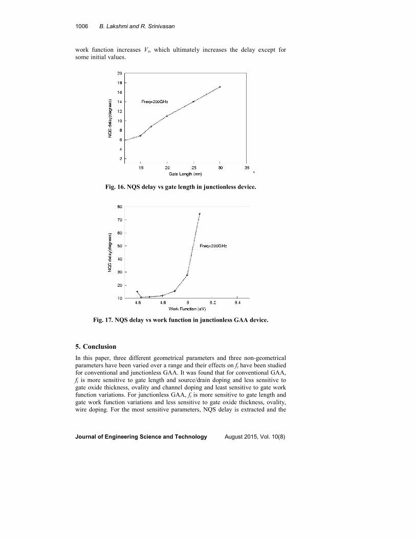
length. As discussed previously, the delay increases monotonically with respect
to gate length for junctionless GAA device also. Figure 17 shows the variation
of NQS delay with respect to gate electrode work function. The increase in the
1006 B. Lakshmi and R. Srinivasan
Journal of Engineering Science and Technology August 2015, Vol. 10(8)
work function increases Vt, which ultimately increases the delay except for
some initial values.
`
Fig. 16. NQS delay vs gate length in junctionless device.
Fig. 17. NQS delay vs work function in junctionless GAA device.
5. Conclusion
In this paper, three different geometrical parameters and three non-geometrical
parameters have been varied over a range and their effects on ft have been studied
for conventional and junctionless GAA. It was found that for conventional GAA,
ft is more sensitive to gate length and source/drain doping and less sensitive to
gate oxide thickness, ovality and channel doping and least sensitive to gate work
function variations. For junctionless GAA, ft is more sensitive to gate length and
gate work function variations and less sensitive to gate oxide thickness, ovality,
wire doping. For the most sensitive parameters, NQS delay is extracted and the

Effect of Process Parameter Variation on ft in Conventional and . . . .1007
Journal of Engineering Science and Technology August 2015, Vol. 10(8)
trend followed by the NQS delay is just the reverse of ft.
Acknowledgement
This work is supported by DRDO, Government of India.
References
1. Singh, N.; Agarwal, A.; Bera, L.K.; Liow, T.Y.; Yang, R.; Rustagi, S.C.;
Tung, C.H.; Kumar, R.; Lo, G.Q.; Balasubramanian, N.; and Kwong, D.L.
(2006). High performance fully depleted silicon nanowire (diameter ≤ 5 nm)
gate-all-around CMOS devices. IEEE Transactions on Electron Device
Letters, 27(5), 383-386.
2. Im, M.; Han, J.W.; Lee, H.; Yu, L.E; Kim, S.; Kim, C.H.; Jeon, S.C.; Kim,
K.H.; Lee, G.S.; Oh, J.S.; Park, Y.C.; Lee, H.M.; and Choi, Y.K. (2008).
Multiple-gate CMOS thin-film transistor with polysilicon nanowire. IEEE
Electron Device Letters, 29(1), 102-105.
3. Clement, J.W.; Suk, S.D.; Li, M.; Yeoh, Y.Y.; Yeo, K.H.; Ha, J.K.; Lim, H.;
Park, H.W.; Kim, D.W.; Chung, T.Y.; Oh, K.S.; and Lee, W.S. (2009).
Characteristics of sub-5 nm trigate nanowire MOSFETs with single and poly
Si channels in SOI structure. Proceedings of VLSI Technology, 142–143.
4. Singh, N.; Lim, F.Y; Fang, W.W.; Rustagi, S.C.; Bera, L.K.; Agarwal, A.;
Tung, C.H.; Hoe, K.M.; Omampuliyur, S.R.; Tripathi, D; Adeyeye, A.O.;
Lo, G.Q.; Balasubramanian, N.; and Kwong, D.L. (2006). Ultra-narrow
silicon nanowire gate-all-around CMOS device: Impact of diameter,
channel-orientation and low temperature on device performance.
Proceedings of IEDM, 1-4.
5. Xiao, D.; Wang, X.; Yu, Y.; Chen, J.; Zhang, M.; Xue, Z.; and Luo, J.
(2009). TCAD study on gate-all-around cylindrical (GAAC) transistor for
CMOS scaling to the end of the roadmap. Journal of Microelectronics,
40(12), 1766-1771.
6. Lee, S.H; Yu, Y.S.; Hwang, S.W.; and Ahn, D. (2009). SPICE-compatible
new silicon nanowire field-effect transistors (SNWFETs) model. IEEE
Transactions on Nanotechnology, 8(5), 643-649.
7. Lai, W.T; Wu, C.W.; Lin, C.C.; and Li, P.W. (2011). Analysis of carrier
transport in trigate Si nanowire MOSFETs. IEEE Transactions on Electron
Devices, 58(5), 1336-1343.
8. Lee, H.; Yu, L.E.; Ryu, S.W.; Han, J.W.; Jeon, K.; Jang, D.Y.; Kim, K.H.;
Lee, J.; Kim, J.H.; Jeon, S.C.; Lee, G.S.; Oh, J.S.; Park, Y.C.; Bae, W.H.;
Lee, H.M.; Yang, J.M.; Yoo, J.J.; Kim, S.I.; and Choi, Y.K. (2006). Sub-5nm
All-Around Gate FinFET for ultimate scaling. Proceedings of VLSI
Technology, 58-59.
9. Zhuge, J.; Wang, R; Huang, R.; Xing, Z.; and Wang, Y. (2008). Investigation
of parasitic effects and design optimization in silicon nanowire MOSFETs for
RF applications. IEEE Transactions on Electron Devices, 55(8), 2142-2147.
10. Ansari, L.; Feldman, B.; Fagas, G.; Colinge, J.P.; and Greer, J.C. (2010).
Simulation of junctionless Si nanowire transistors with 3 nm gate length.
Applied Physics Letters, 97(6), 062105

1008 B. Lakshmi and R. Srinivasan
Journal of Engineering Science and Technology August 2015, Vol. 10(8)
11. Su, C.J.; Tsai, T.I.; Liou, Y.L.; Lin, Z.M.; Lin, H.C.; and Chao, T.S. (2011).
Gate-all-around junctionless transistors with heavily doped polysilicon
nanowire channels. IEEE Electron Device Letters, 32(4), 521-523.
12. Y. Tsividis (2009). Operation and Modeling of the MOS Transistor (2nd
Ed.). Oxford University Press.
13. Synopsys Sentaurus Device User Guide. (2012-13)
14. International Technology Roadmap for Semiconductors. (2012)
15. Lee, C.W.; Borne, A.; Ferain, I.; Afzalin, A.; Yan, R.; Akhavan, N.D.; Razavi, P.;
and Colinge, J.P. (2010). High temperature performance of silicon junctionless
MOSFETs. IEEE Transactions on Electron Devices, 57(3), 620-625.
16. Han, M.H.; Chang, C.Y.; Chen, H.B.; Wu, J.J.; Cheng, Y.C.; and Wu, Y.C.
(2013). Performance comparison between bulk and SOI junctionless
transistors. IEEE Electron Device Letters, 34(2), 169-171.
17. Suryagandh, S.S.; Garg, M.; Gupta, M.; and Woo, J.C.S. (2004). Analog
performance of scaled bulk and SOI MOSFETs. Proceedings of Solid- State
and Integrated Circuits Technology, 153-158.
18. Xiong, S.; and Bokor, J. (2003). Sensitivity of double-gate and FinFET
devices to process variations. IEEE Transactions on Electron Devices,
50(11), 2255-2261.
19. Lakshmi, B.; and Srinivasan, R. (2011). 3D-TCAD simulation study of
process variations on ft in 30 nm gate length FinFET. Proceedings of
ICETECT, 589-593.
20. Lakshmi, B.; and Srinivasan, R. (2012). Investigation of ft and non-quasi-
static delay in conventional and junctionless multi-gate transistors using
TCAD simulations. ARPN Journal of Engineering and Applied Sciences,
7(7), 847-852.
21. Colinge, J.P.; Lee, C.W.; Ferain, I.; Akhavan, N.D.; Yan, R.; Razavi, P.; Yu,
R.; Nazalov, N.; and Doria, R.T. (2010). Reduced electric field in
junctionless transistors. Applied Physics Letters, 96(7), 073510.
22. Allen, F.-L. Ng; Ko, P.K.; and Chan, M. (2002). Determining the onset
frequency of non-quasi-static effects of the MOSFET in AC simulation.
IEEE Electron Device Letters, 23(1), 37-39.