effect of process parameters on the growth of n-polar...
TRANSCRIPT

Effect of Process Parameters on the Growth of
N-polar GaN on Sapphire by MOCVD
A Thesis
Submitted For the Degree of
Doctor of Philosophy
in the Faculty of Science
by
G R Krishna Yaddanapudi
Department of Materials Engineering
Indian Institute of Science
Bangalore 560 012 INDIA
February 2016


Declaration
I hereby declare that the work reported in this thesis is entirely original. It was
carried out by me in the Department of Materials Engineering & Centre for Nano
Science and Engineering (CeNSE), Indian Institute of Science, Bangalore. I further
declare that it has not formed the basis for the award of any degree, diploma,
membership, associateship or similar title of any university or institution.
Date: (G R Krishna Yaddanapudi)
iii

© G R Krishna Yaddanapudi
February 2016
All rights reserved

To My Loving Parents...
v


Abstract
Group III-Nitrides (GaN, InN & AlN) are considered one of the most important
class of semiconducting materials after Si and GaAs. The excellent optical and
electrical properties of these nitrides result in numerous applications in lighting,
lasers, and high-power/high-frequency devices. Due to the lack of cheap bulk III-
Nitride substrates, GaN based devices have been developed on foreign substrates
like Si, sapphire and SiC. These technologies have been predominantly developed
on the so called Ga-polarity epitaxial stacks with growth in the [0001] direction
of GaN. It is this orientation that grows most easily on sapphire by metal organic
chemical vapor deposition (MOCVD), the most common combination of substrate
and deposition method used thus far. The opposite [0001̄] or N-polar orientation,
very different in properties due to the lack of an inversion centre, offers several ad-
vantages that could be exploited for better electronic and optoelectronic devices.
However, its growth is more challenging and needs better understanding.
The aim of the work reported in this dissertation was a systematic investigation
of the relation between the various growth parameters which control polarity, sur-
face roughness and mosaicity of GaN on non-miscut sapphire (0001) wafers for
power electronics and lighting applications, with emphasis on the realization of
N-polar epitaxial layers. GaN is grown on sapphire (0001) in a two-step process,
which involves the deposition of a thin low temperature GaN nucleation layer (NL)
on surface modified sapphire followed by the growth of high temperature device
quality GaN epitaxial layer. The processing technique used is MOCVD. Various
processing methods for synthesis of GaN layers are described with particular em-
phasis on MOCVD method. The effect of ex situ cleaning followed by an in situ
cleaning on the surface morphology of sapphire (0001) wafers is discussed. The
characterization tools used in this dissertation for studying the chemical bond na-
ture of nitrided sapphire surface and microstructural evolution (morphological and
structural) of GaN layers are described in detail.
The effect of nitridation temperature (TN) on structural transformation of non-
miscut sapphire (0001) surface has been explored. The structural evolution of
nitrided layers at different stages of their process like as grown stage and thermal

annealing stage is investigated systematically. The chemical bond environment
information of the nitrided layers have been examined by x-ray photoelectron
spectroscopy (XPS). It is found that high temperature nitridation (TN ≥ 800oC)
results in an Al-N tetrahedral bond environment on sapphire surface. In con-
trast, low temperature nitridation (TN = 530oC) results in a complex Al-O-N
environment on sapphire surfaces. Microstructural evolution of low temperature
GaN NLs has been studied at every stage of processing by scanning electron mi-
croscopy (SEM) and atomic force microscopy (AFM). Surface roughness evolution
and island size distribution of NLs measured from AFM are discussed. It is found
that NLs processed on sapphire wafers nitrided at (TN ≥ 800oC) showed strong
wurtzite [0002] orientation with sub-nanometre surface roughness. In contrast,
NLs processed at (TN = 530oC) showed zinc blende phase in the as grown stage
with higher surface roughness, but acquired a greater degree of wurtzite [0002]
orientation after thermal annealing prior to high temperature GaN growth.
Polarity, surface quality and crystal quality of subsequently grown high temper-
ature GaN epitaxial layers is described in relation to the structure of the trans-
formed nitrided layers. Higher nitridation temperatures (TN ≥ 800oC) consistently
yield N-polar GaN whereas lower nitridation temperatures (TN = 530oC) yield Ga-
polar GaN. It is found that the relative O atom concentration levels in nitrided
layers control the density of inversion domains in N-polar GaN. The effect of var-
ious growth parameters (NH3 flow rate, growth temperature, NL thickness) on
surface morphology and mosaicity of both Ga & N-polar GaN layers is discussed
in detail. We report device quality N-polar GaN epitaxial layers on non-miscut
sapphire (0001) wafers by careful optimization of growth temperature. It is found
that lower growth temperatures (800oC) are favorable for obtaining smooth N-
polar GaN layers. In contrast, N-polar GaN layers grown at higher temperatures
(1000 to 1080oC) are rough with hexagonal hillocks.

Acknowledgements
It has been a great experience to be part of the successful nitride HEMT research
program at IISc. I am sincerely thankful to my adviser Professor Dipankar Baner-
jee, working under him has indeed been a privilege for me and has also been a very
rewarding experience. Sincere thanks to my second adviser Professor Srinivasan
Raghavan early on gave me the opportunity to work in his world class MOCVD
lab, and to get deeply involved with the hardware. Both of them gave me freedom
to explore my own ideas. During the course of my work I was introduced to several
scientific techniques and processes and in the process also I learned a lot about
microstructural analysis from my advisers.
Many thanks to my colleagues (MOCVD growers): Abheek, Hareesh and Naga-
boopathy, who has taught me almost everything I know about MOCVD reactor.
I would also like to thank them, with whom I have spent late growth nights, ma-
chine trouble shooting and repairs.
I would also like to thank staff at micro and nano characterization facility (MNCF)
at CeNSE, IISc and advanced facility for microscopy and micro analysis (AFMM),
comes under the department of Materials Engineering, IISc, for keeping the facil-
ities in good condition and providing training on the equipments.
I am sincerely thankful to my mother and father for their patience and love. Last
but not least, my other colleagues and friends, who has always inspired, motivated,
entertained me during the good and bad times of my PhD study. To all of you.
Thank you.
ix


Contents
Declaration of Authorship iii
Abstract vii
Acknowledgements ix
List of Figures xv
List of Tables xxi
Abbreviations xxiii
1 Introduction 1
1.1 Gallium Nitride . . . . . . . . . . . . . . . . . . . . . . . . . . . . . 1
1.1.1 Substrates for GaN epitaxy . . . . . . . . . . . . . . . . . . 1
1.2 Structure and polarity of GaN . . . . . . . . . . . . . . . . . . . . . 3
1.3 Polarity and growth of GaN . . . . . . . . . . . . . . . . . . . . . . 3
1.3.1 GaN for lighting and power electronic applications . . . . . . 6
1.3.2 Effect of polarity . . . . . . . . . . . . . . . . . . . . . . . . 7
1.4 Thesis description . . . . . . . . . . . . . . . . . . . . . . . . . . . . 10
2 Experimental Techniques for GaN Synthesis & Characterization 13
2.1 Experimental . . . . . . . . . . . . . . . . . . . . . . . . . . . . . . 13
2.1.1 Processing techniques for GaN synthesis . . . . . . . . . . . 14
2.1.2 Metal-organic chemical vapor deposition (MOCVD) . . . . . 15
2.1.3 Time-Temperature (TT) process plot for GaN epitaxy onsapphire by MOCVD . . . . . . . . . . . . . . . . . . . . . . 17
2.2 Characterization . . . . . . . . . . . . . . . . . . . . . . . . . . . . 25
2.2.1 X-ray photoelectron spectroscopy (XPS) . . . . . . . . . . . 26
2.2.2 High resolution x-ray diffractometer . . . . . . . . . . . . . . 27
2.2.3 Atomic force microscopy (AFM) . . . . . . . . . . . . . . . . 29
2.2.4 Differential interference contrast (DIC) light microscopy . . 30
xi

Contents xii
2.2.5 Scanning electron microscopy (SEM) . . . . . . . . . . . . . 32
2.2.6 Transmission electron microscopy (TEM) . . . . . . . . . . . 32
2.2.7 In situ reflectivity and stress monitor analysis tool . . . . . . 33
3 Sapphire Pre-treatment & Microstructural Evolution of LT GaN 37
3.1 Background . . . . . . . . . . . . . . . . . . . . . . . . . . . . . . . 38
3.2 Experimental . . . . . . . . . . . . . . . . . . . . . . . . . . . . . . 39
3.3 Results . . . . . . . . . . . . . . . . . . . . . . . . . . . . . . . . . . 40
3.3.1 In situ thermal treatment of sapphire wafers . . . . . . . . . 41
3.3.2 Nitridation of in situ treated sapphire wafers . . . . . . . . . 43
3.3.2.1 As nitrided sapphire wafers . . . . . . . . . . . . . 43
3.3.2.2 Annealed nitrided wafers . . . . . . . . . . . . . . . 46
3.3.3 LT GaN nucleation layer . . . . . . . . . . . . . . . . . . . . 46
3.3.3.1 Morphological evolution . . . . . . . . . . . . . . . 46
3.3.3.2 Structural evolution . . . . . . . . . . . . . . . . . 50
3.4 Discussion . . . . . . . . . . . . . . . . . . . . . . . . . . . . . . . . 53
3.4.1 Low temperature nitridation (TN = 530oC) . . . . . . . . . . 53
3.4.2 High temperature nitridation (TN = 1100oC) . . . . . . . . . 54
3.5 Summary & conclusions . . . . . . . . . . . . . . . . . . . . . . . . 55
4 Polarity & Microstructural Evolution of HT GaN 57
4.1 Background . . . . . . . . . . . . . . . . . . . . . . . . . . . . . . . 57
4.2 Experimental . . . . . . . . . . . . . . . . . . . . . . . . . . . . . . 61
4.3 Results . . . . . . . . . . . . . . . . . . . . . . . . . . . . . . . . . . 63
4.3.1 Low temperature nitridation (TN = 530oC) . . . . . . . . . 63
4.3.1.1 V/III ratio . . . . . . . . . . . . . . . . . . . . . . 64
4.3.1.2 Growth temperature . . . . . . . . . . . . . . . . . 67
4.3.1.3 LT GaN NL thickness . . . . . . . . . . . . . . . . 69
4.3.1.4 Polarity of HT GaN . . . . . . . . . . . . . . . . . 70
4.3.2 High temperature nitridation (TN = 1100oC . . . . . . . . . 73
4.3.2.1 V/III ratio . . . . . . . . . . . . . . . . . . . . . . 74
4.3.2.2 Polarity of HT GaN . . . . . . . . . . . . . . . . . 75
4.3.2.3 LT GaN annealing time . . . . . . . . . . . . . . . 76
4.3.2.4 Growth temperature . . . . . . . . . . . . . . . . . 78
4.3.2.5 Carrier gas (H2/N2) . . . . . . . . . . . . . . . . . 82
4.3.3 Summary of results . . . . . . . . . . . . . . . . . . . . . . . 82
4.3.3.1 Low temperature nitridation (TN = 530oC) . . . . 83
4.3.3.2 High temperature nitridation (TN = 1100oC) . . . 83
4.4 Discussion . . . . . . . . . . . . . . . . . . . . . . . . . . . . . . . . 84
4.4.1 Low temperature nitridation (TN = 530oC) and HT GaN . . 84
4.4.1.1 Polarity . . . . . . . . . . . . . . . . . . . . . . . . 84
4.4.1.2 Crystalline quality of HT GaN . . . . . . . . . . . 85
4.4.1.3 Surface roughness of HT GaN . . . . . . . . . . . . 86
4.4.2 High temperature nitridation (TN = 1100oC) and HT GaN . 88

Contents xiii
4.4.2.1 Polarity . . . . . . . . . . . . . . . . . . . . . . . . 88
4.4.2.2 Surface quality of HT GaN . . . . . . . . . . . . . 88
4.4.2.3 Crystalline quality of HT GaN . . . . . . . . . . . 91
4.5 Summary & conclusions . . . . . . . . . . . . . . . . . . . . . . . . 92
5 Summary, Conclusions and Future Work 93
A Specifications of MOCVD Reactor 97
Bibliography 99


List of Figures
1.1 Non-centro symmetric wurtzite structure of GaN . . . . . . . . . . 4
1.2 Architecture of HEMT device . . . . . . . . . . . . . . . . . . . . . 9
2.1 Block diagram of MOCVD reactor . . . . . . . . . . . . . . . . . . 15
2.2 Aixtron MOCVD Reactor . . . . . . . . . . . . . . . . . . . . . . . 16
2.3 TT process plot . . . . . . . . . . . . . . . . . . . . . . . . . . . . . 17
2.4 Variation in the equilibrium partial pressure of Ga (PGa) with theinput V/III ratio . . . . . . . . . . . . . . . . . . . . . . . . . . . . 19
2.5 Variation in the equilibrium partial pressure of Ga (PGa) with theinput V/III ratio for our MOCVD experimental conditions. . . . . . 20
2.6 Surface diffusion lengths of Ga adatoms . . . . . . . . . . . . . . . . 24
2.7 Mosaic block model: Tilt & Twist angles . . . . . . . . . . . . . . . 27
2.8 HRXRD goniometer rotational angles . . . . . . . . . . . . . . . . 28
2.9 AFM tip-surface force curve . . . . . . . . . . . . . . . . . . . . . . 29
2.10 DIC light microscopy optical lens diagram . . . . . . . . . . . . . . 32
2.11 k -space MOSS in-situ tool . . . . . . . . . . . . . . . . . . . . . . . 34
2.12 k -space MOSS stress measurement . . . . . . . . . . . . . . . . . . 35
3.1 Surface morphology of sapphire wafers after ex situ cleaning fol-lowed by in situ treatment in MOCVD reactor . . . . . . . . . . . . 41
3.2 Surface morphology of sapphire wafers after ex situ cleaning fol-lowed by in situ treatment in MOCVD reactor . . . . . . . . . . . . 42
3.3 N 1s XPS spectrum of nitrided sapphire wafers . . . . . . . . . . . 43
3.4 Normalized O 1s & N 1s XPS intensities from nitrided sapphire wafers 44
3.5 De-convoluted N 1s XPS spectra from nitrided sapphire wafers . . . 45
3.6 De-convoluted N 1s XPS spectra from nitrided sapphire wafers . . . 47
3.7 SEM morphologies of LT GaN . . . . . . . . . . . . . . . . . . . . . 48
3.8 AFM morphologies of LT GaN . . . . . . . . . . . . . . . . . . . . . 49
3.9 AFM surface roughness of LT GaN . . . . . . . . . . . . . . . . . . 50
3.10 High resolution x-ray (0002) ω-scan profiles for LT GaN NLs . . . . 51
3.11 High resolution x-ray 101̄1 φ-scan profiles for LT GaN NLs . . . . . 52
3.12 High resolution x-ray 101̄1 φ-scan profiles for LT GaN NLs . . . . . 52
4.1 Optical reflectivity trace of GaN on sapphire . . . . . . . . . . . . . 59
4.2 Surface morphology of N-polar GaN . . . . . . . . . . . . . . . . . . 59
xvii

List of Figures xviii
4.3 HRXRD rocking curve FWHM values of N-polar GaN in compari-son to conventional Ga-polar GaN . . . . . . . . . . . . . . . . . . . 60
4.4 Surface morphology of HT GaN (V/III = 485) grown for sapphirenitrided at TN = 530oC . . . . . . . . . . . . . . . . . . . . . . . . . 64
4.5 Surface morphology of HT GaN (V/III = 965, 1055 & 1205)) grownfor sapphire nitrided at TN = 530oC . . . . . . . . . . . . . . . . . 65
4.6 RMS surface roughness data of HT GaN (V/III = 965, 1055 &1205)) grown for sapphire nitrided at TN = 530oC . . . . . . . . . . 66
4.7 growth rate and roughening recovery time of HT GaN samples de-posited at different V/III ratios for sapphire nitridation at TN =530oC. . . . . . . . . . . . . . . . . . . . . . . . . . . . . . . . . . . 66
4.8 HRXRD rocking curve FWHM values of HT GaN samples depositedat different V/III ratios for sapphire nitridation at TN = 530oC. . . 67
4.9 Optical micrographs of HT GaN grown at temperatures (a) 1000oC,(b) 1025oC and (c) 1050oC for sapphire nitridation at TN = 530oC. 68
4.10 AFM surface roughness data of HT GaN layers deposited at growthtemperatures: 1000, 1025 and 1050oCC for nitridation at TN =530oC . . . . . . . . . . . . . . . . . . . . . . . . . . . . . . . . . . 69
4.11 Roughening recovery and growth rate of HT GaN samples grownat different growth temperatures for sapphire nitridation at TN =530oC. . . . . . . . . . . . . . . . . . . . . . . . . . . . . . . . . . . 69
4.12 HRXRD rocking curve FWHM values of HT GaN samples grownat different growth temperatures for sapphire nitridation at TN =530oC. . . . . . . . . . . . . . . . . . . . . . . . . . . . . . . . . . . 70
4.13 AFM surface roughness data of HT GaN as a function of LT GaNNL thickness for sapphire nitridation at TN = 530oC. . . . . . . . . 71
4.14 Roughening recovery time data of HT GaN as a function of LT GaNNL thickness for sapphire nitridation at TN = 530oC. . . . . . . . . 71
4.15 HRXRD rocking curve FWHM values of HT GaN samples grownas a function of LT GaN NL thickness for sapphire nitridation atTN = 530oC. . . . . . . . . . . . . . . . . . . . . . . . . . . . . . . . 72
4.16 SEM morphologies of HT GaN samples before and after KOH etchexperiment for sapphire wafers nitrided at TN = 530oC. . . . . . . . 72
4.17 Nomarski optical microscopy images of HT GaN layers for sapphirewafer nitrided at TN = 1100oC. . . . . . . . . . . . . . . . . . . . . 73
4.18 Nomarski optical microscopy images of HT GaN layers (V/III =965, 1130 & 1205) for sapphire wafer nitrided at TN = 1100oC. . . . 74
4.19 HRXRD rocking curve FWHM values of HT GaN layers (V/III =965, 1130 & 1205) for sapphire wafer nitrided at TN = 1100oC. . . . 75
4.20 SEM morphologies of HT GaN before and after KOH etch experi-ment for sapphire nitridation at TN = 1100oC. . . . . . . . . . . . . 76
4.21 SEM morphologies of HT GaN layers for sapphire nitridation at TN
= 1100oC. . . . . . . . . . . . . . . . . . . . . . . . . . . . . . . . . 77
4.22 SEM morphologies after KOH etch experiment of HT GaN layersfor sapphire nitridation at TN = 1100oC. . . . . . . . . . . . . . . . 78

List of Figures xix
4.23 Optical microscopy images of HT GaN layers grown at differentgrowth temperatures for sapphire nitrided at TN = 1100oC. . . . . . 79
4.24 HRXRD rocking curve FWHM values of HT GaN layers grown attemperatures for sapphire nitridation at TN = 1100oC. . . . . . . . 79
4.25 Optical images of HT GaN layers grown at low growth temperaturesfor sapphire nitridation at TN = 1100oC. . . . . . . . . . . . . . . . 80
4.26 Surface roughness of HT GaN layers grown at low growth temper-atures for sapphire nitridation at TN = 1100oC. . . . . . . . . . . . 82
4.27 Optical images of HT GaN layers grown under N2 as carrier gas forsapphire nitridation at TN = 1100oC. . . . . . . . . . . . . . . . . . 83
4.28 Summary of x-ray rocking curve FWHM values of HT GaN layersover a wide range of growth conditions for sapphire nitrided at TN
= 530oC . . . . . . . . . . . . . . . . . . . . . . . . . . . . . . . . . 85
4.29 SEM morphologies of LT GaN annealed under different flow ratesof NH3 for sapphire nitridation at TN = 530oC. . . . . . . . . . . . 87
4.30 Summary of surface roughness values of HT GaN layers over a widerange of growth conditions for sapphire nitrided at TN = 530oC . . 87
4.31 Normalized O 1s intensity of nitrided sapphire wafers at differentstages for sapphire nitridation at TN = 1100oC. . . . . . . . . . . . 89
4.32 Summary of surface roughness values of HT GaN layers over a widerange of growth conditions for sapphire nitrided at TN = 1100oC . . 90
4.33 Summary of x-ray rocking curve FWHM values of HT GaN layersover a wide range of growth conditions for sapphire nitrided at TN
= 1100oC . . . . . . . . . . . . . . . . . . . . . . . . . . . . . . . . 91


List of Tables
1.1 Properties of various commonly available foreign substrates avail-able for III-Nitride epitaxy . . . . . . . . . . . . . . . . . . . . . . . 2
1.2 Structural information and bond energy of wurtzite GaN . . . . . . 4
1.3 Band gaps of some typical WBG semiconducting materials in rela-tion to Ge and Si. . . . . . . . . . . . . . . . . . . . . . . . . . . . . 7
2.1 Properties of various commonly available processing techniques forIII-Nitride epitaxy . . . . . . . . . . . . . . . . . . . . . . . . . . . 14
2.2 Group-III & V precursors used for III-Nitride epitaxy . . . . . . . . 17
2.3 Vapor pressure constants a and b for common metalorganic precursors 21
2.4 Activation energy EA for decomposition of GaN, and desorption ofGa and N atoms from GaN. . . . . . . . . . . . . . . . . . . . . . . 23
2.5 Surface diffusion barriers for Ga & N adatoms on Ga-polar andN-polar GaN surfaces. . . . . . . . . . . . . . . . . . . . . . . . . . 25
3.1 Normalized intensities of N 1s deconvoluted peaks from various pos-sible nitrided layer structures from TN = 530, 800 & 1100oC. Nor-malization has been done with respect to Al 2p peak. . . . . . . . 45
4.1 HT GaN growth parameter space for sapphire nitridation at TN =530oC . . . . . . . . . . . . . . . . . . . . . . . . . . . . . . . . . . 62
4.2 HT GaN growth parameter space for sapphire nitridation at TN =1100oC . . . . . . . . . . . . . . . . . . . . . . . . . . . . . . . . . . 63
4.3 FWHM values of x-ray rocking curves for the HT GaN samplesgrown directly on LT GaN after ramp up, in relation to the samplesgrown on 4 min annealed LT GaN for sapphire nitridation at TN =1100oC . . . . . . . . . . . . . . . . . . . . . . . . . . . . . . . . . . 78
4.4 The surface roughness values of N-polar HT GaN grown at low &high growth temperatures for sapphire nitridation at TN = 1100oC . 81
4.5 HRXRD rocking curve FWHM values of N-polar HT GaN grownat low & high growth temperatures for sapphire nitridation at TN
= 1100oC . . . . . . . . . . . . . . . . . . . . . . . . . . . . . . . . 81
xxi


Abbreviations
MOCVD Metal Organic Chemical Vapor Deposition
HVPE Hydride Vapor Phase Epitaxy
MBE Molecular Beam Epitaxy
LT Low Temperature
HT High Temperature
NL Nucleation Layer
TMGa Tri Methyl Gallium
TMAl Tri Methyl Aluminium
TMIn Tri Methyl Indium
HEMT High Electron Mobility Transistor
2DEG 2 Dimensional Electron Gas
CTE Coefficient of Thermal Expansion
2D 2 Dimensional
3D 3 Dimensional
SEM Scanning Electron Microscopy
AFM Atomic Force Microscopy
RMS Root Mean Square
XPS X-ray Photoelectron Microscopy
TEM Transmission Electron Microscopy
CBED Convergent Beam Electron Diffraction
HRXRD High Resolution X-ray Diffractometer
XRC X-ray Rocking Curve
FWHM Full Width at Half Maximum
ID Inversion Domains
xxiii

Abbreviations xxiv
QW Quantum Well
SQW Single Quantum Well
LED Light Emitting Diode
DFT Density Functional Theory

Chapter 1
Introduction
1.1 Gallium Nitride
Wide band gap semiconductor Gallium Nitride (GaN) and its ternary and quater-
nary alloys along with InN and AlN, have excellent optical and electrical properties
because of which they have found applications in a range of optoelectronic and
high-power/high-frequency electronic applications [1–3]. In the absence of native
bulk III-Nitride crystals for homo-epitaxy, these materials have been deposited
heteroepitaxially on sapphire, Si and SiC substrates.
1.1.1 Substrates for GaN epitaxy
Table 1.1 tabulates the comparison between various foreign substrates for III-
Nitride epitaxy [2, 4]. Sapphire is the first substrate on which GaN technology
was developed and remains the most favored substrate for optoelectronic applica-
tions such as light emitting diodes (LEDs) in the visible and the upcoming UV
range. The cost is reasonable (non-miscut c-plane wafer) at $ 60 - 70 per 2 inch
wafer. The large lattice mismatch and coefficient of thermal expansion (CTE) mis-
match between GaN and sapphire (0001) results in GaN films with defect density
of the order of ∼ 108 cm−2 with residual stresses that are compressive in nature.
1

Chapter 1. Introduction 2
Property Si Sapphire SiC AlN GaN(111) (0001) (0001) (0001) (0001)
Lattice Mismatch % -16.9 16.02 3.48 2.41 0Available Size 12 8 6 4 2Cost per 2 wafer ∼ 25 ∼ 70 ∼ 1500 ∼ 2000 ∼ 2200Thermal Conductivity κ, W K−1 m−1 148 2.3 49 285 130Biaxial Modulus, GPa 165 458 440 510 470CTE (×10−6), K−1 3.6 5 4.46 3.04 3.94Dislocation Density, cm−2 ∼ 109 ∼ 108 ∼ 108 ∼ 105 ∼ 104
Table 1.1: Properties of various commonly available foreign substrates avail-able for III-Nitride epitaxy
The drawback of sapphire is its low thermal conductivity, which makes it difficult
to dissipate heat from devices during operation.
The alternative substrate, SiC, was for long not suitable for RF devices due to
electrical conductivity in the substrate. In 1999, the first semi-insulating SiC
substrates became available, and SiC has since become the leading substrate for
high-power devices, due to its high thermal conductivity. The other advantage
with SiC is its low lattice mismatch with GaN. The high cost is the major draw-
back for SiC substrates; currently semi-insulating 4H-SiC retails for $ 1200 to 1500
per 2 inch wafer, which is nearly 20 times the cost of sapphire.
The advantage of Si is its availability in large sizes and its cost ( $ 20 to 25 per 2
inch Si (111) wafer). Ga-polar GaN based HEMTs growth on Si (111) is well es-
tablished. The tensile nature of residual stress (due to CTE mismatch) in GaN on
Si (111) results in cracking on cool down unless specific stress mitigating strategies
are adopted. In a very commonly used solution, AlGaN transition layers (graded,
step-graded), are inserted between GaN and Si, to induce compressive growth
stress in the GaN layer to overcome the residual tensile stress on cool down [5–8].
The other drawback with Si is that the GaN layers grown are highly defective
(dislocation density is 1 to 2 orders of magnitude higher than GaN films grown on
sapphire and SiC) due to the large lattice and CTE mismatch.
In summary, all three substrates have their advantages and disadvantages as a
result of which they find their niche areas of technological relevance.

Chapter 1. Introduction 3
This thesis is concerned with growth on sapphire with specific focus on the ability
to control the polarity of GaN. This forms the subject matter of the next section.
1.2 Structure and polarity of GaN
GaN crystallizes in a stable non-centro symmetric wurtzite structure (P63mc) in
addition to a metastable zincblende structure (F4̄3m). The non-centro symmet-
ric wurtzite GaN can either terminate with metal atom (Ga) as the outer layer
along [0001] (+c) direction or anion (N) atom as the outer layer along [0001̄] (-c)
direction (Fig. 1.1 & Table 1.2). For Ga-terminated structure, each Ga atom is
bonded to 3 N atoms below where as for N-terminated structure each N atom is
bonded to 3 Ga atoms below (Fig. 1.1). This apparently simple crystallographic
actually has dramatic consequences for practically every application. As will be
shown in this thesis the growth modes of these two polarities also show very little
resemblance whatsoever to each other. In particular, most current technology has
been developed on Ga-polar GaN based materials as it is the default growth di-
rection. However, the N-polar material which is more difficult to grow, has many
interesting aspects that can enable better power or optoelectronic devices than the
Ga-polar material. Following a brief discussion on the ability of the III-Nitrides to
enable various applications, the high electron mobility transistor, a most common
and simple device is used to illustrate the difference between and the advantage
of the N-polar nitrides in section.
1.3 Polarity and growth of GaN
There are several processing techniques available for III-Nitride materials growth.
Among them metal organic chemical vapor deposition (MOCVD), molecular beam
epitaxy (MBE) and hydride vapor phase epitaxy (HVPE) are commonly used. The
processing technique used in this dissertation is MOCVD available at CeNSE, IISc
Bangalore.

Chapter 1. Introduction 4
Figure 1.1: Non-centro symmetric wurtzite structured GaN with metal-polarity/Ga-polarity and N-polarity.
Property GaN
Lattice Parameters, nm a = 0.319, c = 0.518Space Group P63mcBond Length 1, nm 0.319Bond Length 2, nm 0.319Bond Length 3, nm 0.195Bond Length 4, nm 0.195Bond Length 5, nm 0.518Bond Energy, eV/atom 8.92
Table 1.2: Structural information and bond energy of wurtzite GaN
The process parameters which are associated with the MOCVD reactor are: tem-
perature, pressure, flow rates of group-III precursors for Ga, Al & In, group-V pre-
cursors for N, and carrier gas flow rates (H2 and/or N2). A sapphire pre-treatment
for polarity selection of nitrides, called sapphire nitridation in this dissertation, in-
volves the transformation of sapphire (0001) surface to a thin complex unknown
AlOxN1−x [9] or AlN [10] layer prior to the growth of subsequent nitride layers.
The nitrided layer reduces the chemical dissimilarity between GaN and sapphire
and reduces the lattice mismatch [11, 12], both of which contribute to a reduction
in interface energy, thereby promoting lateral growth. It can act as a wetting layer
for the subsequently grown nitride layers and it can also aid in obtaining the ori-
entation relationships of these with respect to the underlying sapphire substrate
[12–14].

Chapter 1. Introduction 5
The two-step growth process, using MOCVD has been used extensively in im-
proving the structural, optical and electrical quality of nitride epitaxial layers in
particular GaN [15, 16]. This process involves the deposition of a low temperature
(LT) GaN/AlN nucleation layer (NL) on sapphire wafers prior to the deposition of
main high temperature (HT) GaN epitaxial layers. Each of these processing steps
are associated with various growth parameters. The LT NL can be controlled
with parameters like growth time, temperature and flow rates of precursors for
NL deposition. Similar parameter optimisation is required for HT GaN deposition
as well. In the two-step growth method, the LT layer helps to provide nuclei of
an optimum density and orientation for subsequently grown HT GaN layer. The
optimum nucleation density is provided by depositing a thin GaN/AlN NL at low
temperature followed by its controlled annealing. The HT GaN layer then grows
by addition of growth species, N and Ga, to the lateral edges of these nuclei.
While the 2-step method is use for N-polar material as well, fine differences exist.
The growth mechanism of N-polar GaN and its alloys is not the same as Ga-polar
GaN due to their differently terminated surfaces. From total energy density func-
tional theory (DFT) calculations it has been predicted that the Ga and N adatom
surface diffusion barriers are different for Ga-polar GaN and N-polar GaN sur-
faces [17]. Thus, the growth parameters which are optimized for Ga-polar GaN
growth on sapphire are not suitable for N-polar GaN growth. In spite of all the
success achieved with Ga-polar GaN and its alloys, N-polar GaN materials grown
under identical conditions yield rough surface morphology with hexagonal hillocks
[18, 19]. Growth parameters which effect the surface morphology and crystalline
quality of N-polar GaN are reactor pressure (P), carrier gas (H2 and/or N2), V/III
ratio and nitridation temperature (TN). The parameter V/III ratio is simply the
ratio of the fluxes of group-III to group-V precursors which are allowed into the
reactor chamber. The hillock density and size of hillocks on N-polar GaN are very
sensitive to V/III ratio and the density increases with the V/III ratio [18]. Longer
nitridation time also seems to affect the surface morphology of N-polar GaN [19].
It has been shown that N2 carrier gas improves the surface morphology of N-
polar GaN whereas H2 carrier gas suppresses the lateral growth of N-polar GaN

Chapter 1. Introduction 6
[20–22]. The above reports indicate that N-polar GaN growth is very sensitive
to growth parameters, and therefore detailed understanding and careful optimiza-
tion of growth parameters is required to obtain device quality layers. Keller et
al., showed that device quality N-polar GaN epitaxial layers without hexagonal
hillocks can be obtained by using intentionally miscut sapphire (0001) wafers of
2o to 4o along a- and m-directions [23]. However, the cost of highly miscut wafers
are ∼ 4 times the cost of non-miscut sapphire (0001) wafers.
1.3.1 GaN for lighting and power electronic applications
Optoelectronics was the first major application of III-Nitrides that was successfully
commercialized following the pioneering research of Akasaki, Amano and Naka-
mura. Nakamura et al. demonstrated high-brightness blue, green, and yellow light
emitting diodes (LEDs) with InGaN quantum well (QW) structures in 1995 [24].
Ternary InGaN alloys are used as the active layer in GaN-based LEDs and lasers
[24]. The performance of blue and green single quantum well (SQW) structure
LEDs has been improved and at 20 mA, the output power and the external quan-
tum efficiency (EQE) of the blue SQW LEDs were 5 mW and 9.1%, respectively.
Those of green SQW LEDs were 3 mW and 6.3%, respectively [25]. This LED
epitaxial structure is still the basic foundation for all currently commercially avail-
able first-generation blue and green LEDs [25]. It is found that the efficiency of
these LEDs is strongly depends on the In incorporation in the active InGaN layer
[26].
Following optoelectronics, GaN based power electronics and high frequency elec-
tronics is a currently growing area. The GaN based high electron mobility tran-
sistors (HEMTs) has evolved tremendously from their first modest demonstration
in 1993 [27] and is the workhorse of this group of applications. The large band
gaps of GaN and AlGaN provide for large breakdown fields, and thermal stability
of the materials allows for a high temperature of operation [28]. These excellent
properties have led to the demonstrations of devices, with current densities as high
as 2.3 A/mm [29], breakdown voltages around 0.9 kV [30], and power densities of

Chapter 1. Introduction 7
Material Chemical Symbol Band Gap Energy (eV) Type
Germanium Ge 0.7 IndirectSilicon Si 1.1 IndirectGallium Arsenide GaAs 1.4 DirectSilicon Carbide SiC 3.3 IndirectZinc Oxide ZnO 3.4 DirectGallium Nitride GaN 3.4 DirectDiamond C 5.5 DirectAluminum Nitride AlN 6.02 Direct
Table 1.3: Band gaps of some typical WBG semiconducting materials in re-lation to Ge and Si.
41.4 W/mm at 4 GHz [31].
Table 1.3 shows band gaps of some typical wide ban gap semiconductor materials
in relation to Ge and Si [1–3].
1.3.2 Effect of polarity
The tremendous impact of polarity is demonstrated through its effect on the de-
sign and performance of GaN/AlGaN HEMTs. The success of III-Nitride mate-
rial system is not only due to their direct WBG, intrinsic bulk material transport
properties (the p-material properties do not compare well with n-properties in III-
Nitride materials), but also due to the interface properties.
These polar nitrides behave differently across the interface of the active lay-
ers of devices (Fig. 1.2). For example, the difference in polarization across
the Al0.25Ga0.75N/GaN interface, in combination with discontinuity in conduction
band yields a two dimensional electron gas (2DEG) density across the interface,
well in excess of 1 × 1013 cm−2 [32] even in undoped systems. This is in con-
trast to AlGaAs/GaAs HEMTs, where doping is required to form a 2DEG. The
enhancement in the density, mobility and quantum confinement of 2DEG formed
across the interface are some of the primary requirements for HEMT devices. The
following are the parameters which control the properties of 2DEG formed across
the interface

Chapter 1. Introduction 8
� 2DEG carrier density can be enhanced by choosing nitride hetero struc-
tures which have higher discontinuity in polarization across the interface
(like GaN/AlN, of course polarization direction matters).
� The parameters which control 2DEG carrier mobility are surface roughness
of base layer, alloy scattering and critical thickness of AlGaN layer for HEMT
stack and dislocation density level in base layers.
� Quantum confinement of 2DEG can be improved by choosing nitride hetero
structures which give high conduction band discontinuity across the inter-
face.
Ga-polar AlxGa1−xN/GaN HEMTs (the device structure is shown in Fig. 1.2)
yields a 2DEG carrier density across the interface that depends on the composition
’x’ of Al in a thin AlxGa1−xN layer (which is under tension) sitting on GaN (Fig.
1.2a). Usually ’x’ ranges from ∼ 25 to 30%, which in turn limits the critical
thickness of AlxGa1−xN (∼ 25 to 20 nm for x ∼ 25 to 30%). The density of 2DEG
increases with the Al content in AlxGa1−xN due to increased spontaneous and
piezo polarizations in the AlxGa1−xN layer. However, higher Al content results
in formation of cracks in the AlxGa1−xN under tension and degrades the device
performance.
In contrast to the above, the design and architecture of HEMT devices for a
highly confined 2DEG density (> 1013 cm−2) involves the deposition of nitride
materials with N-polarity (Fig. 1.2b) [33]. N-polar GaN/AlGaN HEMTs improve
the confinement of 2DEG due to the WBG AlGaN back barrier (Fig. 1.2b). Strong
confinement results in sharp pinch off voltages.
The other advantages with N-polar GaN based HEMTs are low contact resistance
[34], sharp pinch off voltages due to AlGaN back barrier layers [35, 36]. Higher
trans-conductance can be expected with the same gate channel separation used
for Ga-polar AlGaN/GaN HEMTs [37, 38] as well as higher 2DEG density [2,
33, 39]. N-polar GaN alloy devices have shown impressive performance which
are in comparable to Ga-polar AlGaN/GaN HEMTs in the basic figures of merit
[33, 40].

Chapter 1. Introduction 9
Figure 1.2: Architectures of HEMT devices: (a) conventional Ga-polar Al-GaN/GaN HEMT, (c) shows the corresponding band structure , (b) & (d)N-polar GaN/AlGaN/GaN HEMT and its corresponding band diagram.
It has been also shown that N-polar GaN enhances the In incorporation in the
subsequently grown InGaN QWs on the GaN base layer for LED applications,
which results in LEDs with greater efficiency [41].

Chapter 1. Introduction 10
1.4 Thesis description
The theme of this dissertation is the development and study of N-polar GaN epi-
taxial layers on non-miscut sapphire (0001) wafers for power electronics and light-
ing applications. The processing technique used is MOCVD, available at CeNSE,
IISc Bangalore. The main scope of this thesis is to understand the relation be-
tween various growth parameters which control the polarity, surface roughness
and mosaicity of GaN and epitaxial layers on non-miscut sapphire (0001) wafers.
The various steps of growth such as sapphire nitridation conditions and LT GaN
growth conditions is extensively studied in this work. Growth parameters such as
NH3 flow rate, growth temperature, and NL thickness have been systematically
varied. Particular emphasis is placed on the correlation between the structure of
these precursor layers (nitrided layer and LT GaN NL) on the quality (surface
morphology and mosaicity) and polarity of the subsequently grown nitride semi-
conductor layers. We report for the first time device quality N-polar GaN epitaxial
layers on non-miscut sapphire (0001) wafers.
In chapter 2, various processing methods for synthesis of GaN layers are described
with particular emphasis on MOCVD method. The characterization tools used in
this dissertation for studying the chemical bond nature of nitrided sapphire surface
and micro-structural evolution (morphological and structural) of LT GaN NL &
HT GaN layers are described in detail.
Chapter 3, starts with the effect of ex situ cleaning followed by an in situ cleaning
on the surface morphology of sapphire (0001) wafers. The effect of nitridation
temperature (TN) on structural transformation of non-miscut sapphire (0001) sur-
face has been studied systematically. The structural evolution of nitrided layers
at different stages of their processing like as grown stage and thermal annealing
stage is investigated systematically. The chemical bond environment information
of the nitrided layers has been examined by x-ray photoelectron spectroscopy. It is

Chapter 1. Introduction 11
found that high temperature nitridation (TN ≥ 800◦C) results in a Al-N tetrahe-
dral bond environment on sapphire surface. In contrast, low temperature nitrida-
tion (TN = 530◦C) results in a complex Al-O-N environment on sapphire surfaces.
Micro-structural evolution of LT GaN NLs have been studied at every stage of
processing by scanning electron microscopy and atomic force microscopy. Surface
roughness evolution is measured from atomic force microscopy is described. It is
found that NLs processed on sapphire wafers nitrided at (TN ≥ 800◦C) showed
strong [0002] orientation with sub-nanometer surface roughness. In contrast, NLs
processed at (TN = 530◦C) showed the presence zincblende phase in the as grown
step with higher surface roughness, but acquired a greater degree of wurtzite [0002]
orientation after thermal annealing prior to high temperature GaN growth.
In chapter 4, polarity, surface quality and crystal quality of subsequently grown
HT GaN epitaxial layers is described in relation to the structure of the trans-
formed nitrided layers. High nitridation temperatures (TN ≥ 800◦C) consistently
yield N-polar GaN material whereas low nitridation temperatures (TN = 530◦C)
yield Ga-polar GaN. It is found that the relative oxygen atom concentration levels
in nitrided layers control the density of inversion domains in N-polar GaN layers.
The effect of various growth parameters such as (NH3 flow rate, growth temper-
ature, NL thickness) on surface morphology and mosaicity of both Ga & N-polar
GaN layers is discussed in detail. First time we report device quality N-polar GaN
layers at low growth temperatures 800◦ non-miscut sapphire (0001) wafers.
Chapter 5 contains the summary of the thesis results followed by directions and
suggestions for the future work.


Chapter 2
Experimental Techniques for GaN
Synthesis & Characterization
Group III-Nitride epitaxy on sapphire is a well-established platform and vari-
ety of experimental techniques such as metal organic chemical vapor deposition
(MOCVD), molecular beam epitaxy (MBE) and hydride vapor phase epitaxy
(HVPE) are available to deposit these semiconducting nitride materials. This
chapter contains a brief description of various processing techniques for GaN syn-
thesis with particular emphasis on MOCVD method followed by a brief introduc-
tion to various characterization tools which were used in this dissertation.
2.1 Experimental
The non-miscut 2 inch sapphire (0001) wafers were brought from the following ven-
dors EPISTONE, MONOCRYSTAL and KYOCERA. The unintentional miscuts
of the wafers provided by vendors were in the range of 0 ± 0.3o. The wafers were
diced into 1 cm2 size pieces by a MTI Corporation EC400 wafer dicing saw, which
is furnished with diamond blades of different thicknesses varying from 300 to 100
µm. The saw is computerized with a positional accuracy of 0.01 mm. The diced
wafers were then ultra-sonicated and cleaned ex-situ with acetone, isopropanol
13

Chapter 2. Experimental Techniques & Characterization 14
Property HVPE MBE MOCVD
Growth Rate ∼ 50 µm/h ∼ 50 nm/h ∼ 2 µm/h
Strength Large scale production Sharp interface Large scale productionGood quality film In-situ monitor Sharp interfaceVery high growth rate High purity High purity
H2 free ambient No ultra high vacuumPlasma assisted growth In-situ monitorLaser assisted growth High growth rateUniformity
Weakness Complex process Expensive Expensive sourcesExtreme temperature Need ultra-high vacuum Hazardous sourcesconditionsHazardous sources Low growth rate Large quantities of
NH3 required
Table 2.1: Properties of various commonly available processing techniques forIII-Nitride epitaxy
and de-ionized water. It is observed that the ex situ cleaning procedure is very
critical and it effects the surface morphology of sapphire wafers, as described in
subsequent chapter.
2.1.1 Processing techniques for GaN synthesis
Polycrystalline wurtzite GaN was originally synthesized using HVPE on sapphire
wafers in 1969 [42]. Subsequently several technical breakthroughs enabled single
crystal wurtzite GaN, low residual background carrier concentration in undoped
GaN, conductivity control of p-type GaN, epitaxial layer stacks for LEDs, LDs
and HEMTs, and these led to the first modest LED and HEMT devices being in-
troduced in 1993 [27, 43]. Table 2.1 shows the comparisons between the commonly
available processing techniques used for III-Nitride epitaxy.

Chapter 2. Experimental Techniques & Characterization 15
2.1.2 Metal-organic chemical vapor deposition (MOCVD)
MOCVD is a process for the deposition of materials that utilizes volatile metal
organic compounds to transport metallic atoms that are relatively non-volatile
at the convenient deposition temperature. The organometallic compounds are
usually mixed with other source materials such as Hydrides that react to form
compound semiconductor films. Fig. 2.1 shows the simple block diagram of the
horizontal flow MOCVD reactor. Fig. 2.2 shows the AIXTRON 200/4 RF-S
MOCVD reactor which is installed at CeNSE, IISc.
Figure 2.1: Simple block diagram of horizontal flow MOCVD reactor
The group-III precursors (TMGa, TMAl & TMIn, Table 2.2) are injected into
the reactor chamber with the aid of carrier gas (H2/N2). Group-III & group-V
precursors are injected into the reactor chamber through separate nozzles. The
separation plate inside the chamber prevents the pre-reaction of these precursors.
Eventually, all these precursors are allowed to react onto the substrate surface
which is held at typical growth temperatures. Unwanted products formed will be
pumped to the scrubber for dilution before they are released to the outer atmo-
sphere. The substrate sits on a rotating susceptor to maintain the uniformity of
the deposited film. NH3 is used as the group-V hydride source and H2 used as the

Chapter 2. Experimental Techniques & Characterization 16
Figure 2.2: Aixtron AIX 200/4 RF horizontal flow MOCVD reactor availableat CeNSE, IISc Bangalore.
carrier gas. All the group-III & group-V precursor bubblers and gas lines are fur-
nished with the necessary mass flow controllers (MFCs) and pressure controllers
(PCs) to control the flow rates of gases during the deposition of materials. The
maximum temperature limit of the reactor is 1500oC. The minimum reactor pres-
sure is 10 mbar and the maximum is 1000 mbar. The reactor chamber is equipped
with the removable quartz ware to prevent the reactor walls from contamination
during the growth of materials. The reactor is also equipped with an in-situ real
time thickness and stress monitor tool to understand the stress evolution and
growth behavior of films.

Chapter 2. Experimental Techniques & Characterization 17
Precursor Chemical Formula
Trimethyl Gallium (TMGa) (CH3)3GaTrimethyl Aluminium (TMAl) (CH3)3AlTrimethyl Indium (TMIn) (CH3)3InAmmonia NH3
Carrier Gas H2, N2
Table 2.2: Group-III & V precursors used for III-Nitride epitaxy
2.1.3 Time-Temperature (TT) process plot for GaN epi-
taxy on sapphire by MOCVD
Fig. 2.3 shows the standard time-temperature (TT) process diagram for two-step
GaN epitaxy on sapphire wafers at two different nitridation temperatures TN =
530 and 1100oC.
Figure 2.3: Typical temperature Vs time (TT) process plot for two-step GaNepitaxy on sapphire wafers
The process starts with in situ thermal cleaning of sapphire wafers under the flow
of purified H2 at a temperature of 1100oC. The other process steps which are
involved in GaN epitaxy are
� Nitridation of sapphire at ∼ TN = 500 to 1100oC to enable a structural trans-
formation of sapphire surface to reduce the chemical dissimilarity between
sapphire and subsequently grown GaN layers

Chapter 2. Experimental Techniques & Characterization 18
� LT GaN NL deposition at temperature ∼ 500 to 600oC to provide optimum
nucleation density for the subsequently grown HT GaN epitaxial layers
� Annealing of LT GaN NL at temperature ∼ 1000 to 1080oC involves decom-
position of NLs, surface migration of decomposed atoms, incorporation and
growth of new GaN nuclei.
� Growth of HT GaN epitaxial layer at temperature ∼ 1000 to 1080oC involves
epitaxial layer growth on annealed NLs, with adequate kinetics to grow the
necessary thickness.
The synthesis of GaN by using MOCVD technique is well known [44]. The for-
mation of GaN involves the complex chemical reactions between TMGa, NH3 and
their intermediate gas phase adducts (TMGa:NH3). The corresponding formation
energies for each step in the reaction involves are not documented well. The for-
mation energy of GaN can be estimated by assuming a simple model, where Ga
reacts with the NH3 according to the following reaction [44]
Ga (g) + NH3 (g) ⇔ GaN (s) +3
2H2 (2.1)
The estimated equilibrium constant K for the reaction
K =aGaN .P
3/2H2
PGa .PNH3
(2.2)
and
log10(K) = −12.2 + 1.78 ×(
104
T
)+ 1.79 log10(T) (2.3)
Where aGaN is the activity of GaN, P is the partial pressure of the reactants
which are participating in the above reaction. Fig. 2.4 shows the variation in
equilibrium partial pressures of Ga (PGa) with the corresponding input V/III ratio
[44]. V/III ratio is the ratio of flow rates of input group-V (NH3) and group-III
(Ga, Al & In precursors) sources. The input V/III ratio is varied by changing

Chapter 2. Experimental Techniques & Characterization 19
the partial pressure PNH3 and by keeping PoGa at a constant value. The red color
points indicate the corresponding equilibrium partial pressures of Ga (PGa) for our
MOCVD experimental conditions at two different V/III ratios 260 and 1200.
Figure 2.4: Variation in the equilibrium partial pressure of Ga (PGa) with theinput V/III ratio. Copyright: Koukitu et al., JJAP, Vol.36, L1136, 1997. TheJapan Society of Applied Physics.
Fig. 2.5 shows the variation in equilibrium partial pressure of Ga (PGa) calculated
from equation (2.2) with the V/III ratio for our MOCVD experimental conditions,
which we have used in this dissertation.
It is found that the equilibrium partial pressure of Ga (PGa) decreases with the
increase in V/III ratio.
The driving force for the deposition of GaN is given by equation (2.4) and is
controlled by the partial pressure of NH3 (PNH3) (Fig. 2.4).
∆PGaN = PoGa − PGa (2.4)
Where PGa is the equilibrium partial pressure of Ga inside the reactor chamber,
PoGa is the input partial pressure of Ga which is kept at a constant value. For

Chapter 2. Experimental Techniques & Characterization 20
Figure 2.5: Variation in the equilibrium partial pressure of Ga (PGa) withV/III ratio for our MOCVD experimental conditions.
example in our case, we have kept the corresponding input flow rate of TMGa at
4.1 sccm for GaN growth, and PvGa is the vapor pressure of Ga. Partial pressures
of reactants are varied by changing the corresponding flow rates. We do keep the
TMGa (which is in liquid form) bubbler at a particular temperature where TMGa
is in equilibrium with its vapor. In the subsequent process the carrier gas H2 is
passed through the TMGa bubbler to evaporate liquid TMGa, before it is fed into
the reactor chamber. The input flow rate of TMGa (or PoGa) is controlled by the
flow rate of carrier gas H2 which is passing through the bubbler. The vapor partial
pressure of metal organics (TMGa, TMAl etc.) depends upon the temperature.
The relation can be expressed as [45]
PvIII = 10(a− b
T) × 1013.5
760mbar (2.5)
The vapor pressure for group-III precursors and their corresponding temperatures
are shown in Table 2.3 [45].
The driving force decreases with the decrease in V/III ratio. Three kinds of modes
of deposition is possible [44] from a consideration of Fig. 2.4.

Chapter 2. Experimental Techniques & Characterization 21
Precursor a b (K) Vapor pressure P vIII (mbar)
TMGa 8.07 1703 90 (0oC)TMAl 8.22 2134 9.60 (17oC)TMIn 10.52 3014 1.78 (17oC)
Table 2.3: Vapor pressure constants a and b for common metalorganic pre-cursors
PGa > PoGa: Etching
This mode is achieved by decreasing the V/III ratio or by reducing the partial
pressure of NH3 (PNH3). During this mode GaN starts decomposing and the
decomposition rate is higher than the incorporation rate of Ga and N adatoms
into the growing crystal. GaN decomposes at above 800oC at a pressure of 1 atm
and at lower temperature in vacuum [46, 47]. It was obtained that from mass
spectroscopy and thermogravimetric experiments, GaN decomposes into Ga and
NH3. There is huge scatter in the data reported for the activation energy barrier
for GaN decomposition, which spans from 0.34 to 3.1 eV and depends strongly
on conditions of the ambient (H2 and/or N2) in which the decomposition takes
place [46, 47]. The unit processes involved in GaN decomposition and growth are
explained in the subsequent section.
PGa > PvGa: Droplet formation
As discussed earlier in this context, the equilibrium vapor is the pressure where
the liquid TMGa is in equilibrium with its own vapor. This mode occurs when the
equilibrium partial pressure of Ga (PGa) inside the reactor chamber exceeds the
vapor pressure of Ga (PvGa). During this mode the Ga atoms tend to condense on
the growing surface and eventually form liquid metallic Ga droplets on the surface.

Chapter 2. Experimental Techniques & Characterization 22
PGa < PoGa & PGa < Pv
Ga: Growth
This condition defines the growth window for GaN deposition. During this mode
of growth, the incorporation rate of Ga and N atoms into the growing bulk crystal
is higher than the decomposition rate of GaN. However, the incorporation rate
of adatoms in to the growing crystal is controlled by several factors such as the
life time of adatoms on the growing surface and the diffusion lengths of adatoms
which in turn controlled by the corresponding surface diffusion barriers at typi-
cal MOCVD growth temperatures. The driving force for this growth window is
increases with the increase in partial pressure of NH3 (PNH3), which is consistent
with the experimental MOCVD trends.
The above results indicate that for GaN growth to occur the equilibrium partial
pressure of Ga (PGa) is always has to be lower than the vapor pressure PvGa and
the input partial pressure PoGa.
GaN decomposition has been studied extensively and several mechanisms were
proposed to explain it. The following reactions are reported for GaN decomposi-
tion [48, 49].
2GaN (s) → 2Ga (g) + N2 (g) (decomposition) (2.6)
2GaN (s) → 2Ga (l) + N2 (g) → 2Ga (g) + N2 (g) (desorption) (2.7)
2GaN (s) → GaN (g) or [GaN]x (g) (sublimation) (2.8)
It was reported that H2 could assist the GaN decomposition by reformation of
NH3 via [47].
2GaN (s) + 3H2 (g) → 2Ga (l) + 2NH3 (g) (2.9)
Table 2.4 shows the activation energy barriers measured for the above reactions
under the ambient of H2 [47–49]. The activation energies are measured by sev-
eral techniques such as thermogravimetry, mass spectrometry and reflection high
energy electron diffraction (RHEED).

Chapter 2. Experimental Techniques & Characterization 23
Process EA eV Technique
GaN decomposition 3.1 Thermogravimetry, Mass spectrometryGa desorption from GaN 2.2 - 2.76 RHEED, Growth rate Vs Growth temperatureN desorption from GaN 6.1 RHEED
Table 2.4: Activation energy EA for decomposition of GaN, and desorption ofGa and N atoms from GaN.
The other unit step which takes place in GaN decomposition and growth is surface
diffusion. The factor surface diffusion is critical and it controls the surface quality
of the growing surface.
The mode of growth is classified into two types based on surface diffusion lengths
of the adatoms on the growing surface. The mode step-flow (2D mode) occurs
when the diffusion length of adatoms is longer than the terrace width or step
width involved during growth. In contrast, island mode (3D mode) occurs when
the diffusion length is smaller than the corresponding terrace width [50]. The
diffusion lengths are controlled by the corresponding surface diffusion barriers
at typical process temperatures. The diffusion length can be estimated by the
following equation [50]
λs =√
Dsτs =
(a2 ν= exp
(−Esd
kT
)τs
) 12
(2.10)
Where, Ds is the diffusion coefficient, ν= is vibrational frequency of adatoms paral-
lel to the surface, a is mean distance between the adsorption sites, Esd correspond-
ing surface diffusion activation energy and τs can be classified into two cases, which
are life time before desorption (τD), which depends on the desorption rate and the
life time before lattice incorporation (τI), which depends on growth rate. The
mean life time of residence of adatoms (τD) on the growing surface before being
re-evaporated and is given by
τD =1
ν⊥exp
(Edes
kT
)(2.11)
Where ν⊥ is the vibrational frequency of adatoms normal to the surface and Edes is

Chapter 2. Experimental Techniques & Characterization 24
the desorption activation energy of an adatom from the growing surface. Assuming
ν = ν⊥ = ν=, we have the following expression for surface diffusion length [50]
λs,Ga = a exp
(Edes − Esd
2kT
)(2.12)
Koleske et al. [51] measured λs,Ga based on τD using equation (2.12) and is shown
in Fig. 2.6 as a solid line, which indicates λs,Ga decreases slightly as the temper-
ature increases. This is due to the increase in desorption rate, which results in
reduced τD. But, at typical MOCVD growth pressures Ga desorption appears to
be suppressed and eventually yields longer τD. The limiting life time in such cases
is the incorporation life time (τI) into the growing lattice. The value of τI depends
inversely on growth rate, as slower the growth rate the larger τI.
Figure 2.6: Measured surface diffusion length λs,Ga of Ga adatoms at differenttemperatures. The solid line corresponds to λs,Ga based on τD and dashed linescorrespond to λs,Ga based on τI. Koleske et al., JAP, 84, 1998, 1998. Reprintedwith permission.
Fig. 2.6 shows the dependence of τI on the growth rate and is λs,Ga plotted as
dashed lines for different growth rates ranging from 3 to 100 nm/min. τI was
measured by the thickness per monolayer (actually bilayer, which is 0.258 nm and
represents one half of the lattice parameter along c-direction) by the growth rate. It
was also shown that as growth rate decreases, both and increases, which eventually

Chapter 2. Experimental Techniques & Characterization 25
Adatom Ga-polar GaN Ga-polar GaN N-polar GaN N-polar GaNN-terminated N-terminated
(eV) (eV) (eV) (eV)
Ga 0.4 1.8 0.2 1.0N 1.4 - 0.9 -
Table 2.5: Surface diffusion barriers for Ga & N adatoms on Ga-polar andN-polar GaN surfaces.
yields a more ordered lattice because the number of adatoms that incorporate is
increased. It was found that the diffusion length λs,N for N adatoms is much
smaller than Ga adatoms and is due to the high surface diffusion barrier for N
adatoms when compared to Ga adatoms [17]. At the same time the other possible
reason for lower λs,N values, is due to high vapor pressure of N2, once N migrates
to next to an adjacent N, N2 forms and desorbs.
From total energy density functional theory (DFT) it is predicted that the surface
diffusion barriers for Ga & N adatoms on (0001) and (0001̄) surfaces are not same
[17]. Table 2.5 shows the estimated surface diffusion barriers for Ga & N adatoms
at typical growth temperatures.
From Table 2.4 it can be suggested that the estimated diffusion lengths for Ga &
N adatoms on N-polar GaN surface must be higher than on Ga-polar GaN surface.
As we described in Sec. 1.4.2 of Chapter 1, the surface morphology of N-polar GaN
grown under identical conditions is rough and is associated with inversion domains
(IDs). In such cases the estimation of corresponding surface diffusion lengths of
Ga & N adatoms on both domains (IDs) is complicated, which eventually makes
difficult to understand the behavior of adatoms on the growth surface and hence
the growth mechanism of N-polar GaN.
2.2 Characterization
This section describes some of the standard characterization tools that have been
used to analyze our samples. The primary characterization tools employed in this

Chapter 2. Experimental Techniques & Characterization 26
study are high resolution x-ray diffractometry, x-ray photoelectron spectroscopy,
atomic force microscopy, scanning electron microscopy, differential contrast in-
terference optical microscopy (Nomarski) and the in situ reflectivity and stress
measurement tool. In some cases transmission electron microscopy has been used
to examine the polarity of our samples. All these are available at the Centre for
Nano Science & Engineering (CeNSE), IISc Bangalore. The transmission electron
microscopy studies were done at the Advanced Facility for Microscopy and Micro
analysis (AFMM), IISc Bangalore and Defense Metallurgical Research Laboratory,
Hyderabad.
2.2.1 X-ray photoelectron spectroscopy (XPS)
This technique has been extensively used to study the chemical nature of sap-
phire wafers nitrided at different temperatures. This ex situ tool was supplied
by Kratos Analytical AXIS Ultra DLD, Manchester. It is a surface sensitive tech-
nique, which analyzes the kinetic energy (KE) of photoelectrons which are emitted
from the sample surface via photoemission process. The spectrometer measures
the binding energy (BE) of the ejected electrons from the measured KE. The BE
of the photoelectrons which are emitted from the sample surface is given by the
following relation.
BE = hν − KE − φ (2.13)
Where φ represents the combined electron spectrometer and sample work functions
and is an instrument dependent factor normally derived for each instrument as part
of a calibration procedure. The technique derives its chemical sensitivity from the
fact that nearest neighbor atoms will have a direct effect upon the binding energy
of the core level electrons. Therefore any change in the chemical environment such
as oxidation state will lead to a modification of the KE.
The instrument has the following key components: X-ray source, electron transfer
lens, electron energy analyzer, and detection system. All of these components are
contained within an ultra-high vacuum envelope (10−9 Torr). The spectrometer

Chapter 2. Experimental Techniques & Characterization 27
is equipped with monochromatic x-rays as the primary source. The x-ray gun is
used in combination with a focusing monochromator due to which only the Al
Kα component is diffracted from the quartz crystal. The natural line width of
this component is < 0.26 eV. A charge balance option is available for insulators.
An Ar ion beam was used to clean the sample surface from contamination and/or
for depth profile information. Charge corrections were done with respect to C
1s (Carbon) peak located at 284.8 eV. Elemental quantification of all the survey
spectra and high resolution scans were carried out by CASA XPS software.
2.2.2 High resolution x-ray diffractometer
HRXRD has been used to examine the crystal mosaicity of our samples. The
epitaxial film is assumed to consist of single crystallites called mosaic blocks with
misorientations with respect to each other [52, 53]. The out-of-plane rotation
of the blocks perpendicular to the surface normal is the mosaic tilt, and the in-
plane rotation around the surface normal is the mosaic twist (Fig. 2.7). The
Figure 2.7: Mosaic blocks in a crystal showing tilt and twist with respectto each other. Tilt corresponds to out-of-plane rotation whereas twist corre-sponds to in-plane rotation of mosaic blocks. Srikant et al., JAP, 82, 4286,1997. Reprinted with permission.

Chapter 2. Experimental Techniques & Characterization 28
average absolute values of tilt and twist are directly related to the full width
at half maximum (FWHM) of the corresponding distributions of crystallographic
orientations [52, 53]. The rocking curve measurement (ω-scan) method is the
most frequently employed method to analyze the mosaicity of epitaxial layered
materials. In this geometry, the detector remains stationary and the sample is
rotated about ω-axis (Fig. 2.8).
Figure 2.8: X-ray diffractometer with different rotational angles (ω, ψ, φ) inrelation to the sample reference frame.
ω-scan (000l) reflections are used to measure tilt of mosaic blocks [52, 53]. Tilt is
sensitive to screw and mixed dislocations but not to edge dislocations because edge
dislocations do not distort (000l) planes as their burger vectors (1/3 < 112̄0 >)
lie within those planes. Twist is caused by edge and mixed dislocations and is
usually measured with ω-scans of off-axis reflections (h or k 0). Off-axis reflections
occurring at higher ψ values are used, so that FWHM is dominated by in-plane
twist. Thus, lower FWHM values for (000l) and off-axis reflections indicate that
epitaxial films of better crystalline quality with low mosaicity.
The instrument that has been used for XRC analysis was supplied by RIGAKU
SmartLab, Japan. This tool was equipped with the 2 bounce and 4 bounce Ge
(220) incident beam monochromators. The Cu (Kα1: with λ = 0.15405 nm and
Kα2: with λ = 0.15443 nm) x-ray source is collimated and monochromated by a
4 bounce Ge (220) monochromator to achieve high angular resolution.

Chapter 2. Experimental Techniques & Characterization 29
2.2.3 Atomic force microscopy (AFM)
The AFM used in this dissertation is Dimension Icon ScanAsyst Bruker. The
AFM has been used to study the surface features of LT GaN NLs and the sur-
face roughness evolution of HT GaN epitaxial layers.AFM can be operated in two
modes such as contact mode and non-contact mode. Tapping mode falls in some-
where between the contact and non-contact mode. All AFM measurements were
done in this dissertation using tapping mode technique. The classification of AFM
working modes is described in Fig. 2.9.
Figure 2.9: Typical inter atomic force curve between the cantilever tip ofAFM and sample surface
The contact mode falls in the repulsive interaction region whereas the non-contact
mode falls in the attractive Van der Waals interaction region. The tapping mode
falls somewhere in between the two interaction regions. In the contact mode the
deflection of cantilever is kept constant. In contrast, the tip is oscillated at it’s
resonant frequency in non-contact mode and the amplitude of the oscillation is
kept constant. Contact mode imaging is heavily influenced by frictional and adhe-
sive forces, and can damage samples and distort image data. Non-contact imaging
generally provides low resolution and can also be hampered by the contaminant
(e.g., water) layer which can interfere with oscillation.
Tapping mode imaging takes the positive features of both these modes and over-
comes problems associated with friction, adhesion, electrostatic forces, and other

Chapter 2. Experimental Techniques & Characterization 30
difficulties that plague conventional AFM scanning methods, by alternately plac-
ing the tip in contact with the surface to provide high resolution and then lifting
the tip off the surface to avoid dragging the tip across the surface. Tapping mode
imaging is implemented in ambient air by oscillating the cantilever assembly at or
near the cantilever’s resonant frequency using a piezoelectric crystal. The piezo
motion causes the cantilever to oscillate with a high amplitude( typically greater
than 20nm) when the tip is not in contact with the surface. The oscillating tip is
then moved toward the surface until it begins to lightly touch, or tap the surface.
During scanning, the vertically oscillating tip alternately contacts the surface and
lifts off, generally at a frequency of 50,000 to 500,000 cycles per second. As the
oscillating cantilever begins to intermittently contact the surface, the cantilever
oscillation is necessarily reduced due to energy loss caused by the tip contacting
the surface. The reduction in oscillation amplitude is used to identify and measure
surface features.
When the oscillating cantilever approaches the surface the amplitude of oscillation
decreases. This is due to the additional restoring force works on the cantilever and
this can be seen as an increase in the spring constant of the cantilever. This drop
in amplitude can be used as the feedback parameter for AFM imaging, just like
the cantilever deflection in contact mode.
Tapping mode inherently prevents the tip from sticking to the surface and causing
damage during scanning. Unlike contact and non-contact modes, when the tip
contacts the surface, it has sufficient oscillation amplitude to overcome the tip-
sample adhesion forces. Also, the surface material is not pulled sideways by shear
forces since the applied force is always vertical.
2.2.4 Differential interference contrast (DIC) light microscopy
DIC light microscopy (Nomarski) is a technique which produces impressive 3D-
like images of unstained specimens. The shadowing effects of the technique are
remarkable. DIC light microscopy was used in this dissertation to provide an initial
idea about surface quality of the HT GaN epitaxial layers. Nomarski microscopy

Chapter 2. Experimental Techniques & Characterization 31
utilizes a system of dual beam interference optics that transforms local gradients
in optical path length in a specimen into regions of contrast in an image. The
working principle of the Nomraski light microscope is described in Fig. 2.10
� Light passes through a standard polarizer before entering the condenser,
producing plane-polarized light
� This light enters a Wollaston prism located in the front focal plane of the
condenser. The prism interacts with the polarized light to produce two sep-
arate wavefronts which are parallel and polarized perpendicularly to each
other. These are termed the ordinary (O) and extraordinary (E) rays. Fur-
thermore, these two wavefronts are separated by a very small difference (less
than the resolution of the system) generally ranges from 0.2 - 2 µm and the
separation is depends upon the prism used
� The two wavefronts pass through the specimen, phase of one beam may be
differentially shifted with respect to the other if there is a local gradient in
optical path length.
� The light now enters a second Wollaston prism set-up which recombines the
wavefronts. If there has been a phase shift between the two rays as they
pass through areas of different refractive index then elliptically polarised
light is the result. DIC optics are designed to convert these phase differences
between the two beams of light into amplitude differences which can be
visualized by the human eye
� Finally the light enters a second polarizing filter, termed an analyzer. The
initial polarizer and this analyzer form crossed polars. The analyzer will
permit the passage of some of the elliptically polarized light to form the
final image. All the remaining light will be blocked by the analyzer.

Chapter 2. Experimental Techniques & Characterization 32
Figure 2.10: Typical optical lens diagram of differential interference contrast(DIC) light microscopy. A. Lasslett, Microscopy Division, Olympus UK Ltd,Southall, Middlesex, UK. Reprinted with permission
2.2.5 Scanning electron microscopy (SEM)
The SEM used in this study was Carl Zeiss Ultra 55 FESEM. This tool has been
used to study the morphology of our samples at different stages of their process.
The probe current range: 15 to 20 nA, aperture size range: 7.5 to 120 µm and
accelerating voltage range: 5 to 30 kV.
2.2.6 Transmission electron microscopy (TEM)
TEM was used in this dissertation to examine the polarity of the grown epitax-
ial layers. Convergent beam electron diffraction (CBED) technique was used in
combination with java electron microscope simulator (JEMS) simulated patterns
to examine the polarity of our samples at different thicknesses. A 300 kV Technai

Chapter 2. Experimental Techniques & Characterization 33
TM G2 F30 S-TWIN TEM with FEG at Advanced Facility for Microscopy & Mi-
croanalysis (AFMM) IISc and a FEI Tecnai G2-20T 200KV TEM at Defense Met-
allurgical Research Laboratory (DMRL) Hyderabad were used to examine GaN
layers in this dissertation.
Cross sectional TEM foils were made using the regular sandwich technique, in
which two pieces of the sample are cut and glued together keeping the film sides
of the two pieces facing each other. The sandwich assembly is inserted and stuck
inside a slotted rod and this complete assembly is pushed and glued inside a hollow
tube with 3 mm outer diameter. Thin slices from this combination is cut by using
Buehler ISOMET low speed saw and thinned down to ∼ 100 µm using MULTI-
PREPTM equipment manufactured by Allied Instruments. TEM foils were further
thinned down to electron transparency by using conventional ion-beam thinning
technique using Gatan PIPS (Precision Ion Polishing System) with Cold Stage.
2.2.7 In situ reflectivity and stress monitor analysis tool
The in situ tool that was used in this study is the k -space Associates multi-
beam optical stress sensor (MOSS). This technique has been used to monitor the
growth behavior of GaN films on sapphire. The primary information that can be
extracted is the real time film thickness, real time stress and growth rate. This in
situ capability enables the monitoring of film stress and thickness as it develops.
In the MOSS technique (Fig. 2.11a), multiple parallel laser beams illuminate
the surface simultaneously and the beam positions are measured with a CCD
detector. The measurement of film thickness is based on interference between the
light beams reflected from the top surface of the film and from the film/substrate
interface (Fig. 2.11b). If the film is not too absorbing, interference between the
reflected beams results in a modulation of the reflected intensity. The interference
of beams depends upon the path difference of the rays which in turn depends on
growing film thickness. The period of the intensity oscillations is used to determine
the growth rate of the film. In addition, the amplitude of the intensity oscillations
depends on the reflectivity of the interfaces, and therefore also a probe of surface

Chapter 2. Experimental Techniques & Characterization 34
morphology during growth. Fig. 2.11c shows an example of GaN two-step growth
on sapphire.
Figure 2.11: A schematic diagram of k -space MOSS set up (a) multiple par-allel laser beams fall on the substrate surface and will be reflected and detectedby CCD camera, (b) interference effects for the rays which are reflected fromthe surface and the film/substrate interface, and (c) a sample reflectivity tracefor GaN epitaxy on sapphire, which is recorded by in-situ k -space MOSS toolattached to MOCVD reactor.
The growth rate is measured by
λ
2η= Period of one oscillation (2.14)

Chapter 2. Experimental Techniques & Characterization 35
Where, λ is wavelength of light used = 660 nm.
η is refractive index of the growing film and is 2.3 for GaN.
The in situ tool can also monitor the real time stress evolution in films during their
growth. MOSS stress monitoring is based on measuring the curvature induced in
the substrate by the stressed film (Fig. 2.12).
Figure 2.12: The radius of curvature of the stressed film effects the spacingbetween laser beams which are reflecting from the surface of the film.
The relationship between the film stress, σ , and the radius of curvature, R, is
given by the following equation developed originally by Stoney [54]
σ =Msh
2s
6hfR(2.15)
Where hf is the film thickness, Ms is the biaxial modulus of the substrate, hs is the
substrate thickness, and R is radius of curvature. For flat films R is infinite, so that
parallel beams of light will be reflected from the surface and the beam separation
will be same as the incident beam separation. If a surface is curved, parallel beams
of light that strike it at different positions will be reflected at different angles (Fig.
2.12). The amount of deflection of the light beam is related to the curvature by
1
R=δd
dcosα / 2L (2.16)
Where δd is the measured change in the spacing of the beams, d is the initial
spacing, L is the distance from the sample to the detector and α is the angle
between the incident beams and the surface normal.

Chapter 2. Experimental Techniques & Characterization 36
This tool is used extensively to understand the growth behavior of GaN epitaxial
layers on sapphire (0001) wafers.

Chapter 3
Sapphire Pre-treatment &
Microstructural Evolution of LT
GaN
It is well known that the high energy interface, lattice mismatch and CTE mis-
match between HT GaN and sapphire prevents the HT GaN in growing laterally
and promotes 3-dimiensional growth of GaN with poor crystalline quality. The
structural quality of HT GaN layers is dramatically improved, when a thin LT
GaN/LT AlN NL is deposited on sapphire prior to the growth of HT GaN. The
function of the subsequently grown LT NL could be described as [55]
� The supply of nucleation sites of low orientational fluctuation and
� The promotion of lateral growth of HT GaN
This chapter addresses the following two things. First one is to understand the
structural transformation of sapphire surface at three different nitridation tem-
peratures TN = 530, 800 and 1100oC. Second one is to understand the relation
between the transformed nitrided layers on sapphire surface and the microstruc-
tural evolution of the subsequently grown LT GaN NLs.
37

Chapter 3. Sapphire Pre-treatment & Microstructural Evolution of LT GaN 38
3.1 Background
Nitridation is the foundation of N-polar nitride materials deposited on sapphire
wafers. It is well known that GaN growth on non-nitrided sapphire (0001) surface
results in Ga-polar GaN while that grown on sapphire (0001) surface nitrided in
the temperature range above 950oC results in N-polar GaN [19, 56, 57]. The nitri-
dation of sapphire surface prior to the growth of LT GaN NL is known to reduce
the chemical dissimilarity and lattice mismatch between GaN and sapphire [9–12].
Literature suggests that the nitrided layer is complex unknown AlOxN1−x [9], AlN
and/or AlN in O atom rich environment [10]. Sapphire surface gets damaged if it
is exposed to NH3 and H2 ambient for longer times during nitridation at higher
temperatures [9, 19]. The possible reason behind surface damage is due to the
strong chemical reaction between NH3 and sapphire [19]. Sun et al., showed that
higher nitridation temperatures result in protrusions on sapphire surface during
nitridation, which in turn affects the surface morphology of subsequently grown
N-polar GaN epitaxial layers [19]. The chemical nature and structure of these
protrusions are unknown.
The structural transformation of sapphire surface critically depends upon the pro-
cess conditions such as flow rates of NH3, H2 and/or N2, nitridation temperature
(TN) and process time. It is well known that NH3 decomposes at above 500oC and
the complete decomposition of NH3 is assumed to occur easily at 1100oC [58]. The
mechanism of nitridation involves the counter diffusion of N (inward diffusion) and
O (outward diffusion) atoms from the sapphire surface [58]. Diffusion data for N
and O atoms in sapphire lattice is well documented [58, 59].
It has been reported that the as-grown LT GaN NL on sapphire contains cubic
(zincblende) phase in addition to stable wurtzite phase [59, 60]. The usual tem-
perature range for LT GaN growth falls in between 500 to 600oC [59, 60]. It has
been reported well in the literature that the morphology, distribution, polarity
and orientation of LT GaN critically depends upon the sapphire pre-treatment
called sapphire nitridation in this dissertation. The surface morphology of the as
deposited LT GaN on non-nitrided sapphire wafers is very rough with 3D discrete

Chapter 3. Sapphire Pre-treatment & Microstructural Evolution of LT GaN 39
islands, in contrast the surface morphology is relatively smooth with complete
coverage for the LT GaN deposited on nitrided sapphire wafers [11, 61]. It was
also found that the as grown LT GaN deposited on nitrided sapphire results in
Ga-polar LT GaN and the polarity is transformed to N-polar in the subsequent
annealing steps [57], the polarity of LT GaN is determined by potassium hydroxide
(KOH) etching methods [57]. The annealing of LT GaN NLs take place at typical
GaN epitaxial layer growth temperatures ∼ 1000 to 1080oC under the ambient of
NH3, H2 and/or N2 and it was found that the structural quality of subsequently
grown HT GaN epitaxial layer is a strong function of annealing conditions of LT
GaN [62–66]. N-polar GaN is more sensitive to the ambient present during its
annealing process and it was found that N-polar GaN etches at faster rate than
Ga-polar GaN during annealing period under the ambient of NH3 and H2 at typ-
ical MOCVD annealing temperatures [67]. The crystalline quality and electrical
properties of HT GaN have also been studied as a function of growth rate/thick-
ness of LT GaN NL [63, 68]. The distribution and density of LT GaN nuclei for
the subsequent HT GaN growth can be controlled by the growth parameters such
as V/III ratio and reactor pressure during the growth of LT GaN [62, 69].
This chapter therefore explores the modification of the non-miscut sapphire (0001)
wafers at three nitridation temperatures TN = 530, 800 and 1100oC to provide a
link between GaN two-step growth on non-nitrided sapphire and the conventional
high temperature nitridation.
3.2 Experimental
Experiments were carried out in an Aixtron 200/4 RF-S horizontal flow MOCVD
reactor with removable quartz ware. The in situ thermal treatment of wafers were
carried out at 1100oC under the flow of purified H2 for 10 min before nitridation.
The nitridation step was performed at three different temperatures TN = 530,
800 and 1100oC and 200 mbar reactor pressure. Wafers were nitrided under the
ambient of NH3 and H2 for 1 min. NH3 flow rate was kept constant at 1500 sccm
throughout the process. The nitrided wafers were taken out from the MOCVD

Chapter 3. Sapphire Pre-treatment & Microstructural Evolution of LT GaN 40
reactor chamber for ex situ XPS characterization.
After sapphire nitridation, LT GaN was grown to a 60 nm thick layer to under-
stand the effect of nitridation on microstructural evolution of NL. The thickness
calibration was done by the in situ optical tool as discussed in Sec. 2.2.7 of Chap-
ter 2. The effect of LTGaN thickness on HT GaN growth is described in Chapter
4. LT GaN NL was deposited on nitrided wafers at 530oC for 8 min (to deposit 60
nm thick layer), 200 mbar, at a V/III ratio of 2535, TMGa flow rate of 0.6 sccm
and H2 flow rate of 6500 sccm. The wafers were then heated up from the LT GaN
NL growth temperature to the LT GaN NL annealing condition in 5 minutes. The
NLs were annealed thermally for 4 minutes at 1000oC and a reactor pressure of
400 mbar in a mixture of 2000 sccm of NH3 and 4700 sccm of H2.
During the annealing process of NL, it is possible that the nitrided sapphire surface
regions which are not covered by LT GaN NLs, are exposed to NH3 and nitrided
further. We have investigated these changes by subjecting the nitrided sapphire
surface to identical ramp up and hold cycles as they would encounter during the
deposition of LT GaN NL and its subsequent process. Therefore, after the nitrida-
tion step, the temperature is ramped to the NL deposition temperature of 530oC
and held at 530oC for 8 min followed by temperature ramp up to NL annealing
temperature of 1000oC in 5 minutes. Once the temperature reaches the annealing
condition, it is held for 4 min.
The main tool used to characterize nitrided layers was XPS as described in Sec.
2.2.1 of Chapter 2. SEM & AFM are used for morphological studies, and HRXRD
is for structural analysis of LT GaN NL.
3.3 Results
This section starts with a few results on the effect of ex situ and in situ cleaning on
surface morphology of sapphire (0001) wafers followed by subsequent nitridation
and LT GaN NL deposition steps.

Chapter 3. Sapphire Pre-treatment & Microstructural Evolution of LT GaN 41
3.3.1 In situ thermal treatment of sapphire wafers
As described in Sec. 2.1.3 of Chapter 2, the diced sapphire wafers undergo ex
situ cleaning with acetone, isopropanol and de-ionized water and are dried with
a stream of N2 gas to dry solvents from the surface until no droplets are found.
In many cases, the surface may contain microscopic droplets which might leave
organic residues on the surface upon drying with N2. Fig. 3.1a shows the surface
of sapphire which has been subjected to the ex situ cleaning process with acetone,
isopropanol, de-ionized water and dried with N2 gas prior to the in-situ thermal
cleaning in the MOCVD reactor.
Figure 3.1: Surface morphology of sapphire (0001) wafer which is cleaned exsitu, (a) microscopic organic remnants on sapphire surface after drying with N2
gas, and (b) morphology of sapphire surface after in-situ treatment with H2 at1100oC for 10 min in MOCVD reactor. Fig. (c) & (d) are magnified views of(b).
Fig. 3.1b shows the surface morphology of sapphire after in situ treatment under
the flow of purified H2 at 1100oC. The etched morphology is due to the reaction

Chapter 3. Sapphire Pre-treatment & Microstructural Evolution of LT GaN 42
between H2 and the organic residues which are left after ex situ cleaning [70]. Fig.
3.1c & d are magnified images of in situ treated sapphire surface. To resolve this
issue, we have optimized the ex situ cleaning procedure and it is found that the
cleaning of wafers many times with de-ionized water after acetone and isopropanol
helps to remove all the organic residues from the surface. Fig. 3.2 shows the
surface of sapphire which is cleaned ex situ with acetone, isopropanol and multiple
times with de-ionized water followed by an in situ H2 treatment at 1100oC in the
MOCVD reactor.
Figure 3.2: Surface micrographs of sapphire wafer which have undergone anoptimized ex situ cleaning procedure, (a) & (b) are SEM micrographs at twodifferent magnifications, and (c) & (d) are corresponding AFM morphologieswith sub-nanometre RMS roughness ∼ 0.35 nm.
AFM image shows (Fig. 3.2c & d) atomic steps on the sapphire surface with rms
surface roughness ∼ 0.35 nm after in situ treatment with H2 at 1100oC in the
MOCVD reactor.

Chapter 3. Sapphire Pre-treatment & Microstructural Evolution of LT GaN 43
3.3.2 Nitridation of in situ treated sapphire wafers
3.3.2.1 As nitrided sapphire wafers
Fig. 3.3 shows the high resolution x-ray N 1s photoelectron spectrum from sap-
phire wafers nitrided at three different temperatures TN = 530, 800 and 1100oC.
Figure 3.3: The N 1s x-ray photoelectron peak from sapphire wafers nitridedat TN = 530, 800 and 1100oC
The distinct N 1s binding energy photoelectron peak indicates that there is incor-
poration of N atoms into the sapphire lattice during nitridation. Three effects of
nitridation temperature are discernible: the change in intensity of the N1s peak,
the shift in peak positions and a peak broadening is observed with the decrease
in nitridation temperature. The variation in N1s peak intensity indicates that the
increase in incorporation of N atoms into the sapphire surface with the nitridation
temperature. The shift in peak position and peak broadening indicates that the
environment of the N atoms in the modified sapphire undergoes changes with ni-
tridation temperature. Since surface modification is expected to occur by inward
diffusion of N into sapphire to replace O atoms. Fig. 3.4 shows the normalized

Chapter 3. Sapphire Pre-treatment & Microstructural Evolution of LT GaN 44
intensities of N 1s and O 1s peaks and are plotted against nitridation tempera-
tures. The normalization is done with respect to the Al 2p peak intensity. Increase
in nitridation temperature results in greater N/O ratios in the modified sapphire
surface.
Figure 3.4: Normalized intensities of (a) O 1s and (b) N 1s peaks from sapphirewafers nitrided at TN = 530, 800, and 1100oC. Normalization was done withrespect to Al 2p peak
The normalized O 1s intensity is compared with the O 1s intensity from non-
nitrided sapphire surface as indicated by blue color line in Fig. 3.4b. It is found
that the non-nitrided sapphire surface has high O atom content when compared
to nitrided sapphire surfaces. Peak broadening and shift in peak positions have
been explored by deconvoluting the N1s peaks. Fig. 3.5 shows the deconvoluted
spectra of N 1s photoelectron peaks at different nitridation temperatures.
Systematic changes in both the intensity and peak positions are observed with the
change in nitridation temperature. A strong peak at ∼ 396.7 eV is present for TN
=800 and 1100oC (Fig. 3.5b & c). This coincides with that of the binding energy
of Al-N bond in the bulk AlN of 396.7 eV [58, 71] and indicates the structural
transformation of sapphire surface to AlN at TN ≥ 800oC. There are additional
peaks at ∼ 398.5 eV and ∼ 395.5 eV. The intensity of the former peak decreases
and the latter increases with the change in nitridation temperature from TN =
800 to 1100oC. The peaks at ∼ 395 eV correspond to sub-stoichiometric AlNx<1
with Al-Al bonds [72]. The peak at ∼ 398 eV has been attributed to incomplete

Chapter 3. Sapphire Pre-treatment & Microstructural Evolution of LT GaN 45
Figure 3.5: De-convoluted spectra of N 1s photoelectron peaks from sapphirewafers nitrided at (a) TN = 530oC, (b) TN = 800oC, and (c) TN = 1100oC.
TN AlN (Al-N bond) AlON (Spinel) AlOxN1−x Sub-stoichiometricAlN (Al-Al bond)
(oC) IN1s (a. u.) IN1s (a. u.) IN1s (a. u.) IN1s (a. u.)
530 0.30 0.13 1.81 -800 1.2 - 0.8 0.251100 1.34 - 0.35 0.55
Table 3.1: Normalized intensities of N 1s deconvoluted peaks from variouspossible nitrided layer structures from TN = 530, 800 & 1100oC. Normalizationhas been done with respect to Al 2p peak.
substitution of O by N such that tetrahedral A-N-O bonds are present [58, 73].
With decrease in nitridation temperature, peak positions shift to higher energy
levels. At TN = 530oC, the binding energy of 401.41 eV indicates that N is in O
atom rich environment [59, 74–77] and the peak at 405.31 eV in Fig. 3.5a arises
from AlON cubic spinel structure [76]. Table. 3.1 summarizes these results in the
form of normalized intensities of N 1s deconvoluted peaks from various possible
nitrided layer structures from TN = 530oC to 1100oC. Normalization has been
done with respect to Al 2p peak.

Chapter 3. Sapphire Pre-treatment & Microstructural Evolution of LT GaN 46
3.3.2.2 Annealed nitrided wafers
The XPS plots shown in Fig. 3.6 suggest that the as-nitrided layers undergo
further nitridation during ramp and anneal conditions. For TN = 530oC, the N 1s
peak just after ramp up to the annealing temperature shifts toward lower energy
levels indicating a transitional bonding environment with decreasing amount of
O atom content, and tetrahedral Al-N bond formation (Fig. 3.6a). The peak
corresponds to 405 eV (AlON cubic spinel) is no longer observed after ramp up
and anneal step.
It is found that after 4 min anneal step the dominant peak located at 397.4 and
is corresponds to the Al-N bond energy levels in O atom rich environment (Fig.
3.6c). In contrast, no significant changes are observed for the samples that have
been nitrided at TN = 1100oC as shown in Fig. 3.6b & 3.6d. The dominant peak
is always found to be at ∼ 396.7 eV that corresponds to tetrahedral Al-N bonds
in bulk AlN [58, 71]. The minor peak located at ∼ 398 eV in as-nitrided sample
is found to remain even after ramp up step (Fig. 3.6b), but has shifted to ∼ 397
eV after 4 min annealing step (Fig. 3.6d). Fig. 3.6e shows the compiled binding
energy scale for the N 1s photoelectron peak with their corresponding chemical
bond environments from the literature [58, 59, 71–77] .
3.3.3 LT GaN nucleation layer
3.3.3.1 Morphological evolution
Fig. 3.7 shows the surface morphology of LT GaN NL after the three different
stages: deposition, ramp up to LT GaN annealing temperature of 1000oC in 5
minutes (0 min annealing) and hold at 1000oC for 4 minutes (4 min annealing).
Fig. 3.8 shows the corresponding AFM morphologies. Fig. 3.9 shows the RMS
surface roughness values of the NLs derived from AFM data.
The most striking aspect of the LT GaN NLs evolution summarized in Fig. 3.7 to
3.9 is the significant difference in surface morphology and AFM roughness between

Chapter 3. Sapphire Pre-treatment & Microstructural Evolution of LT GaN 47
Figure 3.6: N 1s x-ray photoelectron peaks from nitrided sapphire wafers atdifferent stages of their process: (a) & (c) are for TN = 530oC, after ramp up and4 min annealing, and (b) & (d) are for TN = 1100oC, after ramp up and 4 minannealing at 1000oC. The compilation of N 1s binding energy scale with theircorresponding chemical bonding environments are shown in (e) [58, 59, 71–77]
NLs deposited on surfaces nitrided at TN = 530oC versus those deposited on
surfaces nitrided at TN ≥ 800oC. A levelling effect of the ramp up and anneal
at higher temperatures can be seen from Fig. 3.7 & 3.9. On sapphire nitrided
at TN = 530oC, Fig. 3.7a, the nuclei appears to be arranged along the atomic
steps on sapphire and evolve in this arrangement even during the ramping step.

Chapter 3. Sapphire Pre-treatment & Microstructural Evolution of LT GaN 48
Figure 3.7: SEM surface morphologies of LT GaN NLs: (a), (b) & (c) are forthe NL at different stages of their processing on sapphire wafers nitrided at TN
= 530oC, (d), (e) & (f) are for the NL processed on sapphire wafers nitride atTN = 800oC, (g), (h) & (i) are for the NL on sapphire wafers nitrided at TN =1100oC.

Chapter 3. Sapphire Pre-treatment & Microstructural Evolution of LT GaN 49
Figure 3.8: AFM surface morphologies of LT GaN NLs: (a), (b) & (c) are forthe NL at different stages of their processing on sapphire wafers nitrided at TN
= 530oC, (d), (e) & (f) are for the NL processed on sapphire wafers nitride atTN = 800oC, (g), (h) & (i) are for the NL on sapphire wafers nitrided at TN =1100oC.

Chapter 3. Sapphire Pre-treatment & Microstructural Evolution of LT GaN 50
Figure 3.9: AFM surface roughness evolution of LT GaN NLs deposited onsapphire wafers nitrided at TN = 530, 800 and 1100oC at different stages oftheir processing.
However, further exposure to NH3 at higher temperatures 1000oC during the hold
step annihilates these preferential orientations of the islands. In the case of the
samples nitrided at TN = 800 and 1100oC the ramp up significantly smoothens the
LT GaN surface. However annealing appears to lead to an element of preferential
sublimation leaving behind features that appear in light contrast.
3.3.3.2 Structural evolution
The effect of nitridation on the crystallography of the LT GaN NLs is revealed
through the HRXRD scans of Fig. 3.10 to 3.12. Fig. 3.10. Shows (0002) HRXRD
ω-scan profiles of LT GaN NLs at different stages of their processing. It is clearly
seen that the NL deposited on surfaces nitrided at TN ≥ 800oC show strong (0002)
peaks as compared to that deposited on the surface nitrided at TN = 530oC. The
LT GaN processed on sapphire nitrided at TN ≥ 800oC is found to be wurtzite
LT GaN with a strong [0002] orientation as indicated by six {101̄1} asymmetric
peaks shown in Fig. 3.11c and d. The sample is tilted to 61.96o about ψ-axis and
is rotated 360o about φ-axis to get diffraction from six {101̄1} planes. NLs at the
end of their 4 min annealing step have significantly reduced in thickness and it is

Chapter 3. Sapphire Pre-treatment & Microstructural Evolution of LT GaN 51
difficult to pick up an XRD signal from them.
In contrast, the NLs grown on sapphire nitrided at TN = 530oC does not show
this strong [0002] orientation in the as-grown conditions as indicted by the φ-
scan in Fig. 3.11a. This is due to the presence of zincblende phase. Fig. 3.12
shows the phi scan measurements for cubic LT GaN {220} peaks. Six {220} peaks
which are separated by 60o angle indicates the presence of zincblende phase in
the as grown LT GaN. The sample is tilted to 35.26o about the ψ-axis and the
detector is fixed at 2θ of 57.91o to get the diffraction from {220} planes. However
{101̄1} peaks appear after the 4 min annealing step at 1000oC (Fig. 3.11b),
indicating that decomposition and reformation of GaN during this process results
in transformation of LT GaN from zincblende phase to wurtzite phase with [0002]
oriented crystallography.
Figure 3.10: High resolution x-ray (0002) ω-scan profiles for NL at differentstages of their processing: (a) is for as grown LT GaN NL on sapphire surfacesnitrided at TN = 530, 800 and 1100oC, (b) is for NL after the 0 min annealingconditions and (c) is for NL after 4 min annealing.
The results indicate that HT nitridation of sapphire yields LT GaN NL with
strong [0002] orientation. In contrast LT nitridation yields LT GaN NL with the
zincblende in the as grown step and transformed to wurtzite phase with [0002]
orientation in the subsequent anneal stages.

Chapter 3. Sapphire Pre-treatment & Microstructural Evolution of LT GaN 52
Figure 3.11: High resolution x-ray {101̄1} diffraction φ-scan for NLs: (a), (b)are for NLs processed on sapphire wafers nitrided at TN = 530oC, (c), (d) arefor NLs processed on sapphire wafers nitrided at TN = 1100oC.
Figure 3.12: High resolution x-ray diffraction φ-scan measurements forzincblende {022} peak of as-grown LT GaN on sapphire nitrided at TN = 530oC.

Chapter 3. Sapphire Pre-treatment & Microstructural Evolution of LT GaN 53
3.4 Discussion
3.4.1 Low temperature nitridation (TN = 530oC)
The as nitrided surface at low nitridation temperatures shows a relatively high O
atom content with a strong N1s peak at ∼ 401 eV accompanied by less intense
peaks at ∼ 405 eV and ∼ 397 eV as shown in Fig. 3.5a. These peaks have been
identified with various levels of O in AlN [58, 59, 71–77] (Fig. 3.6e). It appears
plausible to state that the surface is dominated by Al2O3 based structural motifs
on nitridation at TN = 530oC accompanied by small amounts of AlON cubic spinel
associated with the peak at ∼ 405 eV [76].
The deposition of LT GaN on such a surface results in zincblende GaN with (111)
orientation and an incomplete coverage of the surface (Fig 3.7a). The possible
reason for incomplete coverage of LT GaN is due to incomplete nitridation of
sapphire at low temperatures. It has been shown earlier that GaN deposited
on unnitrided sapphire is rough with 3D islands and with incomplete coverage
[11]. This is due to the high energy interface between GaN and sapphire [11].
Therefore we believe that the high energy interface between GaN and sapphire
is not significantly affected by low temperature nitrided layer and we continue to
obtain 3D islands of GaN with incomplete coverage. The possible reason for the
directionality of LT GaN (Fig. 3.7a) is due to the nucleation of LT GaN along the
atomic steps of the sapphire surface (Fig. 3.2). However the ramp up and anneal
process provides a more complete coverage along with distinct texturing along the
[0002] axis of wurtzite GaN (Fig 3.7c & 3.11b). The ramp up and anneal steps
are accompanied by N1s peak shifts from the underlying nitrided surface (Fig. 3.5
and 3.6), the uncovered portions of which are exposed to H2 and NH3 ambient
at higher temperatures of 1000oC. As we described in Sec. 2.1.3 of Chapter 2,
during ramp up and anneal stages LT GaN starts decompose and redeposits on
sapphire surface, which is in the ambient of NH3 and H2. The decomposition
and redeposition of LT GaN involves the surface migration of decomposed Ga and
N adatoms, and incorporation of these adatoms into the newly formed growing

Chapter 3. Sapphire Pre-treatment & Microstructural Evolution of LT GaN 54
nuclei and/or on the existing nuclei, which eventually yields LT GaN with different
surface morphology when compared to the as grown stage (Fig. 3.7a, b & c).
It appears that the decomposition and redeposition of GaN occurs on further
nitrided region complexes which are now rich in N atom content, given that the
high intensity N1s photoelectron peak has a value of ∼ 397 eV which corresponds
to Al-N bond in O atom environment (Fig. 3.6). Therefore, it is plausible to
state that the increase in coverage of LT GaN during ramp up and anneal steps is
due to reduction in interface energy between GaN and sapphire via changes in the
transformed structure of underlying nitrided layer from AlOxN1−x to dominant
Al-N bond in O atom environment. It also appears that this process leads to the
formation of wurtzite LT GaN oriented along [0002] direction (Fig. 3.11b).
3.4.2 High temperature nitridation (TN = 1100oC)
At higher nitridation temperatures (TN = 800 and 1100oC) there is adequate ni-
trogen from the decomposed NH3 source to completely replace the O atoms in
sapphire surface [58], and stable Al-N bonds will be formed due to complete ex-
change of N and O atoms in sapphire surface [78]. This is indicated by the high
intensity XPS N1s peak at 396.7 eV, which corresponds to that of Al-N binding
energy in bulk AlN [58, 71]. There is no significant change in this structure of ni-
trided layer on annealing after ramp up as shown in Fig 3.6. As a consequence LT
GaN deposited on such surfaces after high temperature nitridation results in strong
[0002] oriented wurtzite LT GaN with complete surface coverage in as grown and
annealed stages (Fig. 3.7d & g and 3.11c & d). The complete coverage of LT GaN
is due to the transformed nitrided layer (Al-N bond environment), which results in
reduced interface energy between GaN and sapphire, and eventually promotes 2D
growth of LT GaN. It has been shown that nitrided layer acts as wetting layer and
it reduces the interface energy between GaN and sapphire [61]. Thus, we believe
that the complete coverage of LT GaN on sapphire nitrided at temperatures TN ≥
800oC (Fig. 3.7d & g) is due to the wetting nature of transformed nitrided layer.
The surface coverage of LT GaN is complete even after ramp up stage also, but

Chapter 3. Sapphire Pre-treatment & Microstructural Evolution of LT GaN 55
the morphology contains pits of various size. The possible reason for the pits of
various size is due to the polarity of LT GaN layer. It was reported that N-polar
GaN decomposes rapidly in the ambient of NH3 & H2 than Ga-polar GaN [67].
We suspect that the as grown LT GaN contains GaN of both polarities and in the
subsequent ramp up process the N-polar domains etch at faster rate than Ga-polar
domains, which eventually leads to pits in the LT GaN of various size (Fig. 3.7e &
h). The surface morphology at the end of the anneal step contains islands of small
in size with bright contrast (Fig. 3.7f & i), are could be remnants of Ga-polar
LT GaN, which have been left after etch of N-polar LT GaN. The strong [0002]
orientation of wurtzite LT GaN is also due to the transformed Al-N bond nitrided
layer which reduces the lattice mismatch between GaN and sapphire, and aids the
NL in forming with the [0002] orientation with respect to the underlying substrate
[58, 59, 71–73].
Therefore, we state that the structural evolution of nitrided layer plays an im-
portant role in determining the morphology, surface coverage and orientation of
subsequently grown LT GaN NL with respect to the underlying sapphire substrate.
3.5 Summary & conclusions
Chemical bond evolution of transformed nitrided layers on sapphire surfaces have
been investigated systematically at different stages of their processing. It is found
that HT nitridation (TN = 1100oC) yields modified sapphire surface with Al-N
bond rich environment. In contrast LT nitridation yields (TN = 530oC) sapphire
surface modified with the dominant Al2O3 based structural motifs in the as grown
stage and transformed to Al-N bond with O atom content. The effect of these
seed layers on the microstructural evolution of subsequently grown LT GaN NLs
have been studied systematically. It is observed that the morphology, surface
coverage and orientation of LT GaN NL strongly depends on the evolution of
the transformed nitrided layer on sapphire surface. LT GaN NLs processed on
HT nitrided sapphire are found to have strong [0002] orientation with complete
surface coverage. In contrast, LT GaN processed on LT nitrided sapphire showed

Chapter 3. Sapphire Pre-treatment & Microstructural Evolution of LT GaN 56
zincblende phase with incomplete coverage in the as grown stage and later it got
transformed to wurtzite phase with [0002] orientation and with enhanced surface
coverage after the subsequent ramp up and anneal steps.

Chapter 4
Polarity & Microstructural
Evolution of HT GaN
This chapter focuses on the following two points, the first one is to understand
the relation between the structure of the transformed nitrided layer on sapphire
and polarity of the subsequently grown two-step HT GaN epitaxial layers. The
second one is to understand the relation between various growth parameters such
as growth temperature, V/III ratio, LT GaN parameters and carrier gas etc., on
the surface morphology and crystalline quality of HT GaN layers.
4.1 Background
The influence of various growth parameters on microstructural evolution of HT
GaN layers can be easily understand by monitoring the in-situ optical reflectivity
traces as discussed in subsequent Sec. 2.2.7 of Chapter 2. Fig. 4.1 shows one such
reflectivity trace of GaN two-step epitaxy on sapphire. Different processing stages
are indicated in relation to the two-step process.
� Stage 1 corresponds to the pre-treatment of sapphire wafers. During this
period wafers are thermally annealed at 1100oC under the ambient of H2
57

Chapter 4. Polarity & Microstructural Evolution of HT GaN 58
followed by sapphire nitridation step. During this stage the reflectivity stays
constant at sapphire reflectivity (0.07595). The optical reflectivity trace is
normalized to bare sapphire reflectivity.
� Stage 2, starts with the deposition of LT GaN NL at 530oC. The rise in
reflectivity is due to change in refractive index from sapphire to GaN and
the reflectivity continues to increase due to interference effects of optical rays
from LT GaN and sapphire.
� In stage 3, the as deposited LT GaN layer is annealed thermally at 1000oC
under the ambient of H2 and NH3. This stage involves several steps such
as decomposition of LT GaN, surface migration of decomposed Ga and N
adatoms and redeposition of GaN nuclei. All these steps eventually lead to
roughening of LT GaN surface and reduction in the thickness of LT GaN
layer [62, 79]. The reason for the drop in reflectivity shown in Fig. 4.1 is due
to roughness as well as reduction in thickness of annealed LT GaN [62, 79].
� Stage 4, starts with the deposition of HT GaN at 1000oC, 400 mbar. During
this stage HT GaN starts growing in island mode (3D) and the reflectivity
drops to a minimum due to high surface roughness of the sample [69, 80].
The reflectivity continues to stay at a minimum until the coalescence of HT
GaN islands occur. The coalescence of islands lead to recovery in optical re-
flectivity and after this point the HT GaN starts grow in layer by layer mode
(2D) [69, 80]. The time duration between the point where the reflectivity
hits a minimum and where the reflectivity recovers is called roughening re-
covery period. This period is a direct measure of crystalline quality of HT
GaN and is sensitive to the growth parameters.
� In stage 5, HT GaN starts grow in layer by layer mode (2D mode). The
oscillations in the reflectivity trace is due to interference effects of the optical
rays which are reflected from GaN surface and GaN/sapphire interface. The
period of oscillation gives the growth rate of the film as discussed in Sec.
2.2.7 of Chapter 2.

Chapter 4. Polarity & Microstructural Evolution of HT GaN 59
Figure 4.1: In-situ optical reflectivity trace of two-step GaN epitaxy on sap-phire (0001) wafers.
In spite of all the success achieved with Ga-polar GaN and its alloys, the surface
morphology of N-polar GaN films grown under identical conditions, are rough
with hexagonal facets and are not suitable for device fabrication [18] (Fig. 4.2).
Intentionally miscut sapphire (0001) wafers (2o to 4o) along a- and m-directions
were used to obtain device quality N-polar GaN layers as shown in Fig. 4.2b
[23]. Fig. 4.3 shows the HRXRD rocking curve FWHM values of N-polar GaN
layers grown on miscut and non-miscut nitrided sapphire wafers in comparison to
conventional Ga-polar GaN layers [19].
Figure 4.2: Surface morphology of N-polar GaN layers grown on (a) non-miscut and (b) highly miscut nitrided sapphire wafers. Sumiya et al., JAP, 88,1158, 2000. Keller et al., JAP, 102, 083546, 2007. Reprinted with permission.

Chapter 4. Polarity & Microstructural Evolution of HT GaN 60
Figure 4.3: High resolution x-ray diffraction rocking curve FWHM values forN-polar GaN in comparison to conventional Ga-polar GaN. Sun et al., JCG,311, 2948, 2009. Reprinted with permission.
Although the growth mechanism of Ga-polar GaN has been clarified to a great
extent, this knowledge can not be applied to N-polar GaN directly, because the
surface structures of Ga-polar GaN and N-polar GaN are not the same. The sur-
face diffusion barriers for Ga and N adatoms are different on Ga-polar GaN and
N-polar GaN surfaces [17]. It is suggested that the rough surface morphology of
N-polar GaN is due to mixed polar domains and the hillock formation is due to
difference in growth rates of Ga-polar and N-polar domains [81]. The centre of the
hillock is found to be terminate with Ga-polar domain whereas the surrounding
matrix is termonated with N-polar GaN [81]. These inversion domains (IDs) are
found to originate from the regions which are rich in O atom content [82, 83].
They are also found to originate from GaN/sapphire film interface [82, 83] and
also from the steps on the sapphire surface [84]. However, by careful optimization
of growth parameters such as nitridation temperature Sun et al. obtained rela-
tively smoother N-polar GaN films [19]. Device quality N-polar GaN layers were
obtained on intentionally miscut (2o to 4o) sapphire (0001) wafers [19, 23]. Inten-
tionally miscut wafers (2o to 4o) enhances the mobility of adatoms significantly
and when the step density is high the probability of incorporation Ga adatoms at
the step edges is high and it results in a step flow growth mode. At lower step
densities (0.5o to 1o) the distance between adjacent steps is large and it results in

Chapter 4. Polarity & Microstructural Evolution of HT GaN 61
nucleation of islands on terraces between steps [23].
Therefore, it is plausible to state that the surface quality of N-polar GaN is con-
trolled by the following two factors
� Surface mobility of adatoms on the growth surface, which is controlled by
the miscut of sapphire wafers [23].
� Density of IDs, which is controlled by both the O atom content on the
nitrided surface and miscut of sapphire wafers [82–84].
However, to date there are no reports on systematic analysis of polarity selection
and microstructural evolution of LT GaN NLs and HT GaN layers in relation to
the structure of the transformed nitrided layers on sapphire wafers. This chap-
ter addresses the factors which control the surface morphology of N-polar GaN
through surface mobility of adatoms and density of IDs on non-miscut sapphire
(0001) wafers.
4.2 Experimental
The in situ thermal treatment of wafers were carried out at 1100oC under the flow
of purified H2 for 10 min before nitridation. The nitridation step was performed
at three different temperatures TN = 530, 800 and 1100oC and 200 mbar reactor
pressure. Wafers were nitrided under the ambient of NH3 and H2 for 1 min. NH3
flow rate was kept constant at 1500 sccm throughout the process.
After sapphire nitridation, LT GaN was grown to a 60 nm thick layer to under-
stand the effect of nitridation on microstructural evolution of NL. The thickness
calibration was done by the in situ optical tool as discussed in Sec. 2.2.7 of Chap-
ter 2. LT GaN NL was deposited on nitrided wafers at TN = 530oC for 8 min
(to deposit 60 nm thick layer), 200 mbar, at a V/III ratio of 2535, TMGa flow
rate of 0.6 sccm and H2 flow rate of 6500 sccm. The wafers were then heated up
from the LT GaN NL growth temperature to the LT GaN NL annealing condition
in 5 minutes. The NLs were annealed thermally for 4 minutes at 1000oC and a

Chapter 4. Polarity & Microstructural Evolution of HT GaN 62
Parameter A1 A2 A3 A4 A5
LT GaN Thickness, nm 60 60 60 60 to 605
LT GaN Anneal Time, min 4 4 4 4 4
LT GaN Anneal, NH3 flow, sccm 2000 3000 to 4000 4000 47005000
HT GaN Growth Temperature, oC 1000 1000 1000 to 1000 10001050
HT GaN Growth Pressure, mbar 400 400 400 400 400
HT GaN TMG flow, sccm 4.1 4.1 4.1 4.1 4.1
HT GaN NH3 flow, sccm 2000 3000 to 4000 4000 47005000
HT GaN V/III ratio 485 725 to 1205 965 965 1135
HT GaN Thickness, µm ∼ 1.5 ∼ 1.5 ∼ 1.5 ∼ 1.5
HT GaN Carrier gas H2 H2 H2 H2 H2
Table 4.1: HT GaN growth parameter space for sapphire nitridation at TN =530oC
reactor pressure of 400 mbar in a mixture of 2000 sccm of NH3 and 4700 sccm of H2.
Several growth parameters are varied to understand the polarity and micro-structural
evolution of HT GaN layers. These are tabulated in Table 4.1 & 4.2. Table 4.1
corresponds to growth parameters for sapphire nitridation at TN = 530oC and
Table 4.2 is for growth parameters at TN = 1100oC.

Chapter 4. Polarity & Microstructural Evolution of HT GaN 63
Parameter B1 B2 B3 B4 B5 B6 B7
LT GaN Thickness, nm 60 60 60 60 60 30 60
LT GaN Anneal Time, min 4 4 4 0 4 0 4
LT GaN Anneal 2000 3000 to 4700 4700 4700 1500 4700NH3 flow, sccm 5000
HT GaN Growth 1000 1000 1000 1000 1000 to 900 1000Temperature, oC 1050 800
HT GaN Growth 400 400 400 400 400 400 400Pressure, mbar
HT GaN TMG flow, sccm 4.1 4.1 4.1 4.1 4.1 2.0 4.1
HT GaN 2000 3000 to 4700 4700 4700 1500 4700NH3 flow, sccm 5000
HT GaN V/III ratio 485 725 to 1135 1135 1135 750 11351205
HT GaN Thickness, µm ∼ 1 ∼ 1 ∼ 1 ∼ 1 ∼ 1 ∼ 1
HT GaN Carrier gas H2 H2 H2 H2 H2 H2 N2
Table 4.2: HT GaN growth parameter space for sapphire nitridation at TN =1100oC
4.3 Results
4.3.1 Low temperature nitridation (TN = 530oC)
Fig. 4.4a shows the surface morphology of HT GaN layer deposited on 4 min
annealed LT GaN for sapphire wafer nitrided at TN = 530oC (Fig. 3.7c of Chapter
3), as per growth conditions given in column A1 of Table 4.1, that is at a V/III
ratio of 485. The morphology is quite rough and is due to incomplete coalescence
of HT GaN islands. The corresponding reflectivity trace is shown in Fig. 4.4b.
There is no recovery in reflectivity due to high surface roughness of the film. Red
color point on the trace indicates the starting point of HT GaN growth.

Chapter 4. Polarity & Microstructural Evolution of HT GaN 64
Figure 4.4: Surface morphology of HT GaN grown for sapphire nitrided atTN = 530oC, at a V/III ratio of 485 and its corresponding optical reflectivitytrace.
To enhance the island coalescence and to obtain device quality HT GaN epitaxial
layers for the nitridation temperature of TN = 530oC we have systematically varied
several growth parameters such as V/III ratio, growth temperature of HT GaN
and LT GaN thickness/growth time. The effect of each of these growth parameters
on surface and microstructural evolution of HT GaN will be described in the
subsequent sections.
4.3.1.1 V/III ratio
V/III ratio is the ratio of input flow rates of group-V (NH3) and group-III pre-
cursors (TMGa, TMAl & TMIn). V/III ratio is varied in this dissertation by
keeping the TMGa flow rate constantly at 4.1 sccm. NH3 flow rate is varied from
2000 to 5000 sccm. Fig. 4.5 shows the surface morphologies of HT GaN layers
grown at different V/III ratios with their corresponding reflectivity traces. The
corresponding growth conditions are given in column A2 of Table 4.1.
Fig. 4.6 shows the corresponding RMS surface roughness data of these samples.
The surface roughness is found to be increase to 0.75 nm (V/III = 1205) from 0.5
nm (V/III = 965).

Chapter 4. Polarity & Microstructural Evolution of HT GaN 65
Figure 4.5: Nomarski optical micrographs of HT GaN surfaces and their cor-responding in-situ optical reflectivity traces, grown at V/III ratios (a) 965, (b)1055 and (c) 1205 for a nitridation temperature of TN = 530oC. In all tracesthe red points indicate starting point of HT GaN growth.
The information that we extract from the reflectivity traces shown in Fig. 4.5 are
the corresponding growth rates and the roughening recovery times of HT GaN. It
is found that the growth rate of HT GaN decreases with the increase in V/III ratio.
The growth rate can be obtained from the period of the reflectivity oscillations as
described in the Sec. 2.2.7 of Chapter 2.
It is also found that the roughening recovery time decreases with the increase
in V/III ratio. Fig. 4.7 shows the variation in the growth rate and roughening
recovery time of HT GaN layers plotted against the V/III ratios.
The mosaicity of all these HT GaN samples were characterized by HRXRD. Fig.
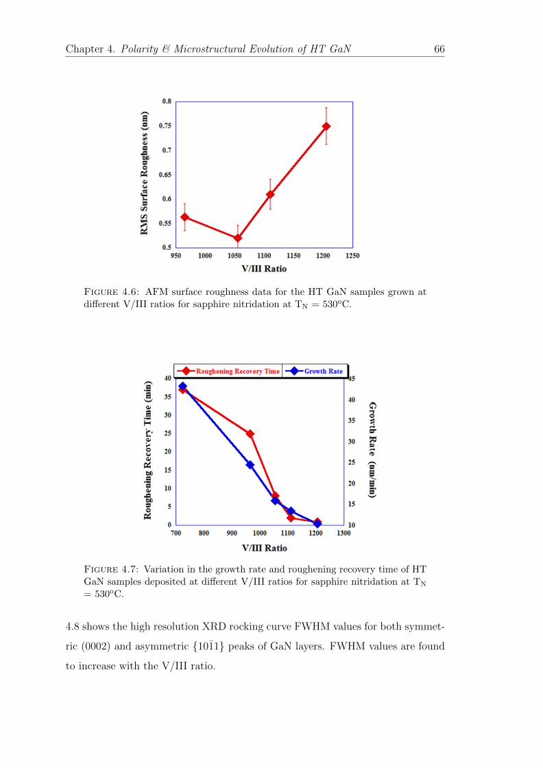
Chapter 4. Polarity & Microstructural Evolution of HT GaN 66
Figure 4.6: AFM surface roughness data for the HT GaN samples grown atdifferent V/III ratios for sapphire nitridation at TN = 530oC.
Figure 4.7: Variation in the growth rate and roughening recovery time of HTGaN samples deposited at different V/III ratios for sapphire nitridation at TN
= 530oC.
4.8 shows the high resolution XRD rocking curve FWHM values for both symmet-
ric (0002) and asymmetric {101̄1} peaks of GaN layers. FWHM values are found
to increase with the V/III ratio.

Chapter 4. Polarity & Microstructural Evolution of HT GaN 67
Figure 4.8: High resolution XRD rocking curve measurements for HT GaNsamples grown at different V/III ratios for sapphire nitrided at TN = 530oC.
The results suggest that the surface quality and crystalline quality of HT GaN
layers depends critically on the V/III ratio.
4.3.1.2 Growth temperature
The other growth parameter which controls the surface morphology of HT GaN
is the growth temperature. We have varied HT GaN growth temperature from
1000oC to 1050oC using the growth parameters given in column A3 of Table 4.1.
Fig. 4.9 shows the surface morphology of HT GaN layers with their corresponding
reflectivity traces for sapphire nitridation of TN = 530oC. Fig. 4.10 shows the
corresponding surface roughness evolution of HT GaN layers. The roughness is
found to be decrease with the increase in growth temperature.
Fig. 4.11 shows the corresponding changes in growth rate and roughening recovery
time of the HT GaN layers. A slight increase in the growth rate of HT GaN is
observed. In contrast, it is found that the roughening recovery time decreases to
∼ 1 min from ∼ 25min and this is due to the faster coalescence of HT GaN islands
at higher growth temperatures.

Chapter 4. Polarity & Microstructural Evolution of HT GaN 68
Figure 4.9: Nomarski optical micrographs of HT GaN surfaces and their cor-responding in-situ optical reflectivity traces, grown at temperatures (a) 1000oC,(b) 1025oC and (c) 1050oC for sapphire nitridation at TN = 530oC. In all tracesthe red points indicate starting point of HT GaN growth.
Interestingly, we did not find any significant change in the crystalline quality
(mosaicity) of HT GaN samples grown at different growth temperatures. Fig.
4.12 shows the HRXRD rocking curve FWHM values for symmetric (0002) and
asymmetric {101̄1} peaks.

Chapter 4. Polarity & Microstructural Evolution of HT GaN 69
Figure 4.10: AFM surface roughness evolution of HT GaN layers deposited atgrowth temperatures: 1000, 1025 and 1050oCC for nitridation at TN = 530oC.
Figure 4.11: Variation in roughening recovery and growth rate of HT GaNsamples grown at different growth temperatures for sapphire nitridation at TN
= 530oC.
4.3.1.3 LT GaN NL thickness
In order to improve the crystalline quality of HT GaN layers further we have
systematically varied the thickness/growth time of LT GaN NLs to control the

Chapter 4. Polarity & Microstructural Evolution of HT GaN 70
Figure 4.12: High resolution XRD rocking curve FWHM values for symmetric(0002) and asymmetric {101̄1} peaks of HT GaN samples grown at differentgrowth temperatures for sapphire nitridation at TN = 530oC.
nucleation density (process conditions: column A4 of Table 4.1). Fig. 4.13 shows
the RMS roughness as a function of LT GaN thickness. The roughness is insensitive
to thickness except at very low thicknesses where it rises sharply. Fig. 4.14 shows
the roughening recovery rate which decreases with the increase in thickness. The
FWHM values are found to be lowest for 25 nm thickness of LT GaN NL (Fig.
4.15). The optimum thickness of LT GaN and the optimum process parameters
are may not be same for all the reactors and it may vary for different reactor
geometries.
4.3.1.4 Polarity of HT GaN
It is well known from the literature that the HT GaN samples grown on non-
nitrided sapphire consistently yield Ga-polar GaN. Potassium hydroxide (KOH)
etching and convergent electron beam diffraction (CBED) experiments were car-
ried out on these HT GaN samples for polarity measurement. It is known from the
literature that KOH etches the N-polar GaN whereas Ga-polar GaN is resistant to
KOH etch [85–88]. The HT GaN samples are etched in 0.2 mol of KOH solution

Chapter 4. Polarity & Microstructural Evolution of HT GaN 71
Figure 4.13: AFM surface roughness data of HT GaN as a function of LTGaN NL thickness for sapphire nitridation at TN = 530oC.
Figure 4.14: Roughening recovery time data of HT GaN as a function of LTGaN NL thickness for sapphire nitridation at TN = 530oC.
at 60oC for 10 min. Fig. 4.16 shows the surface morphology of HT GaN samples
before and after KOH etching experiment.
It can be seen that HT GaN samples are not significantly affected by the KOH
treatment as shown in Fig. 4.16a and 4.16b. The experimental CBED patterns
were taken along < 101̄0 > zone axis of GaN and the patterns were compared
with JEMS simulated patterns. The JEMS patterns were simulated for different

Chapter 4. Polarity & Microstructural Evolution of HT GaN 72
Figure 4.15: High resolution XRD rocking curve FWHM values for symmetric(0002) and asymmetric {101̄1} peaks of HT GaN samples as a function of LTGaN NL thickness for sapphire nitridation at TN = 530oC.
Figure 4.16: Surface morphologies (a) before and (b) after KOH etch experi-ments of HT GaN layers grown on annealed NLs for sapphire wafers nitrided atTN = 530oC. The corresponding convergent beam electron diffraction patternsalong with their cross-sectional images of GaN films are shown in (c).

Chapter 4. Polarity & Microstructural Evolution of HT GaN 73
thicknesses 110 and 145 nm from the GaN/sapphire interface. The 0002 disc
indicates a bright band at the center whereas 0002̄ disc indicates a dark band
at the center for Ga-polar GaN film. These etching results and CBED patterns
shown in Fig. 4.16c indicate that the two-step HT GaN layers grown on surfaces
nitrided at TN = 530oC are Ga-polar GaN [19, 85–89].
4.3.2 High temperature nitridation (TN = 1100oC
)
Fig. 4.17 shows the surface morphology of HT GaN layer deposited on 4 min
annealed LT GaN NL for sapphire wafers nitrided at TN = 1100oC (column B1
of Table 4.2 ). The morphology is quite rough and contains hexagonal faceted
islands. The corresponding reflectivity trace is shown in Fig. 4.17b. There is no
recovery in the reflectivity due to high surface roughness of the film.
Figure 4.17: Nomarski optical microscopy images of HT GaN layers for sap-phire wafer nitrided at TN = 1100oC. The corresponding reflectivity trace isalso shown in the figure. The red point on the trace indicates the starting pointof HT GaN growth.
Immediately after HT GaN growth reflectivity rises substantially and then drops
down to a minimum after two small oscillations. This indicates that HT GaN starts
with a 2D growth mode at the beginning of the growth and then in the subsequent
process the growth mode is transformed to a 3D mode. We have varied several

Chapter 4. Polarity & Microstructural Evolution of HT GaN 74
growth parameters to enhance the surface quality of HT GaN layers. These studies
are described below.
4.3.2.1 V/III ratio
Fig. 4.18 shows the Nomarski optical microscopy images of HT GaN layers grown
at different V/III ratios of 965, 1130 and 1205. The corresponding growth param-
eters are given in column B2 of Table 4.2
Figure 4.18: Nomarski optical microscopy images of HT GaN layers depositedat V/III ratios (a) 965, (b) 1130 and (c) 1205 for sapphire nitridation at TN =1100oC.
In all cases the surface morphology is rough with faceted hexagonal islands. The
corresponding reflectivity traces are not shown here because there was no recovery
in the reflectivity traces due to high surface roughness. It has been shown earlier
that higher V/III ratio can enhance the surface quality of HT GaN for sapphire ni-
tridation at TN = 530oC. In contrast, for HT GaN samples for sapphire nitridation
at TN = 1100oC, the surface morphology remains rough with faceted hexagonal
islands and with small changes in the density and size of the islands for the given
V/III ratio range.
Fig. 4.19 shows the FWHM values of x-ray rocking curves of grown HT GaN
samples at different V/III ratios for sapphire nitridation at TN = 1100oC. FWHM
values of (0002) and {101̄1} peaks are found to increase with the V/III ratio.

Chapter 4. Polarity & Microstructural Evolution of HT GaN 75
Figure 4.19: High resolution XRD rocking curve FWHM values for HT GaNlayer: (a) (0002) and (b) {101̄1} peaks for sapphire nitridation at TN = 1100oC.
4.3.2.2 Polarity of HT GaN
The surface morphology of HT GaN layers for high nitridation temperatures is
rough with many hexagonal hillocks as shown in Fig. 4.17 & 4.18. Prior to
further optimization of HT GaN layers, potassium hydroxide (KOH) etching and
convergent electron beam diffraction (CBED) experiments were carried out on
these HT GaN samples for polarity measurement. HT GaN samples are etched
in 0.2 mol of KOH solution at 60oC for 10 min. Fig. 4.20 shows the surface
morphology of HT GaN samples before and after KOH etching experiment. The
growth conditions for the samples are given in column B3 of Table 4.2
The etching and CBED studies indicate that the samples grown on annealed NL
for sapphire wafers nitrided at TN = 1100oC are N-polar GaN. As can be seen
from Fig. 4.20a and 4.20b, they are substantially etched away when subjected
to the same KOH etch treatment [85–88]. CBED patterns shown in Fig. 4.20c
confirm that they are N-polar [19, 89]. The CBED patterns were taken along
< 101̄0 > zone axis of GaN and the patterns were compared with the JEMS
simulated patterns. The JEMS patterns were simulated for different thicknesses
100, 105 and 115 nm from the GaN/sapphire interface. In this case both 0002
disc and 0002̄ discs are interchanged in contrast due to N-polarity of GaN film as

Chapter 4. Polarity & Microstructural Evolution of HT GaN 76
Figure 4.20: Surface morphologies (a) before and (b) after KOH etch experi-ments of HT GaN layers grown on annealed NLs for sapphire wafers nitrided atTN = 1100oC. The corresponding convergent beam electron diffraction patternsalong with their cross-sectional images for GaN films are shown in (c).
compared to the TN = 530oC case (Fig. 4.16). The hillock remnants which are
left after KOH etch are Ga-polar since they do not etch.
4.3.2.3 LT GaN annealing time
The rough surface morphology with faceted hexagonal islands seen in the previous
section may originate from mixed polarities of HT GaN. It has been suggested in
the literature that the faceted hexagonal hillocks originate from inversion domains
in the structure that is from Ga polar domains that grow faster than the sur-
rounding N-polar domains [81]. It has also been suggested that Ga-polar domains
form on O atom rich surfaces [82, 83]. It was thought that the annealing period
at the high temperature nitridation may enhance the O atom level on the nitrided
surface as a consequence of diffusion from the sapphire substrate into the nitrided
layer. To enhance the surface quality of HT GaN layers we have grown these layers
on samples that were ramped up to the growth temperature but not annealed.

Chapter 4. Polarity & Microstructural Evolution of HT GaN 77
Fig. 4.21 shows the Nomarski optical microscopy images of HT GaN layers grown
under identical conditions except the LT GaN annealing time (column B4 of Table
4.2). The sample shown in Fig. 4.21a is deposited on 4 min annealed LT GaN as
described in previous sections. In contrast, HT GaN grown on samples directly af-
ter ramp up without annealing results in a substantial reduction of the hexagonal
hillock density (Fig. 4.21b).
Figure 4.21: Surface morphologies of HT GaN layers deposited on (a) 4 minannealed LT GaN layer and (b) as ramped up LT GaN layers for sapphirenitridation at TN = 1100oC.
To confirm the polarity in the HT GaN that was deposited in the as-ramped up
condition, the above samples are subjected to same KOH etch treatment. Fig. 4.22
shows the side view of SEM surface morphologies of HT GaN epitaxial layers shown
in Fig. 4.21a and 4.21b, after KOH etch experiment. Both process conditions lead
to N-polar GaN. However, the density of the remnant hillocks after the KOH
etching were significantly less for the HT GaN grown directly after ramp up (Fig.
4.22b), that is the smoother HT GaN was associated with a lower density of
remnant hillocks (Fig. 4.21b). The results suggest that device quality N-polar
GaN layers can be obtained on non-miscut sapphire (0001) wafers.
Table 4.3 shows the HRXRD rocking curve FWHM values for the sample grown
directly on LT GaN after ramp up, in relation to the samples grown on 4 min
annealed LT GaN for sapphire nitridation at TN = 1100oC.

Chapter 4. Polarity & Microstructural Evolution of HT GaN 78
Figure 4.22: Surface morphologies of HT GaN layers after KOH treatmentdeposited on (a) 4 min annealed LT GaN layer and (b) 0 min annealed (rampedup) LT GaN layers for sapphire nitrided at TN = 1100oC.
Layer LT GaN LT GaN (0002) {101̄1}Thickness Anneal Time FWHM FWHM
(nm) (min) (arc-sec) (arc-sec)
HT GaN 60 4 702 2523HT GaN 60 0 540 1130
Table 4.3: FWHM values of x-ray rocking curves for the HT GaN samplesgrown directly on LT GaN after ramp up, in relation to the samples grown on4 min annealed LT GaN for sapphire nitridation at TN = 1100oC
4.3.2.4 Growth temperature
The other process parameter which we have varied to control the surface mor-
phology of HT GaN is the growth temperature. We have varied HT GaN growth
temperature as described in the previous section from 1000oC to 1050oC. The cor-
responding growth parameters are listed in column B5 of Table 4.2.
It is found that the size and density of hexagonal islands are very sensitive to
growth temperature (Fig. 4.23). The density of islands is found to increase while
the size of the hexagonal islands is found to decrease with the increase in growth
temperature.
Fig. 4.24 shows the corresponding HRXRD rocking curve FWHM values. The
FWHM values of (0002) and {101̄1} are found to be increase with the growth

Chapter 4. Polarity & Microstructural Evolution of HT GaN 79
Figure 4.23: Nomarski optical microscopy images of HT GaN layers grownat (a) 1000oC, (b) 1025oC and (c) 1050oC growth temperatures for sapphirenitrided at TN = 1100oC.
temperature.
Figure 4.24: HRXRD rocking curve FWHM values of HT GaN layers grownat temperatures: (a) 1000oC, (b) 1025oC and (c) 1050oC growth temperaturesfor sapphire nitridation at TN = 1100oC.
Since density and size of hexagonal islands critically depends upon the growth
temperature and is found to increase with the growth temperature. In order to
understand further the surface evolution of N-polar GaN layers, we have also grown
HT GaN samples at lower growth temperatures < 1000oC. Fig. 4.25 shows the
Nomarski optical images of HT GaN layers grown at two different temperatures
of 900 and 800oC as per the growth conditions given in column B6 of Table 4.2.
Interestingly, the reflectivity oscillations were observed for the sample grown at

Chapter 4. Polarity & Microstructural Evolution of HT GaN 80
Figure 4.25: Optical surface images of HT GaN layers grown at differenttemperatures (a) 900oC, (b) 800oC (LT GaN annealed at 800oC) and (c) 800oC(LT GaN annealed at 1000oC). The corresponding in-situ optical reflectivitytraces are also shown.
temperature 800oC (Fig. 4.25b). The sample surface looks mirror like. In con-
trast, in the sample grown at 900oC, decay in the reflectivity oscillations has been
observed (Fig. 4.25a) and the corresponding surface morphology of the sample
looks relatively rougher than the sample grown at 800oC. The results indicate
that lower growth temperatures < 1000oC seems to be favorable for obtaining N-
polar GaN with good surface quality. These samples are subjected to the same

Chapter 4. Polarity & Microstructural Evolution of HT GaN 81
Layer LT GaN LT GaN LT GaN HT GaN SurfaceThickness Anneal Anneal Growth Roughness
Time Temperature Temperature(nm) (min) (oC) (oC) (nm)
HT GaN 60 4 1000 1000 RoughHT GaN 60 0 1000 1000 ∼ 3.5HT GaN 30 0 800 800 ∼ 1.5HT GaN 30 0 1000 800 ∼ 1.2HT GaN 30 0 900 900 ∼ 7.5
Table 4.4: The surface roughness values of N-polar HT GaN grown at low &high growth temperatures for sapphire nitridation at TN = 1100oC
Layer LT GaN LT GaN HT GaN (0002) {101̄1}Thickness Anneal Growth FWHM FWHM
Temperature Temperature(nm) (oC) (oC) (arc-sec) (arc-sec)
HT GaN 60 1000 1000 702 2523HT GaN 60 1000 1000 820 2182HT GaN 30 800 800 1080 2160HT GaN 30 1000 800 540 1800
Table 4.5: HRXRD rocking curve FWHM values of N-polar HT GaN grownat low & high growth temperatures for sapphire nitridation at TN = 1100oC
KOH treatment described in the earlier sections and are confirmed to be N-polar.
The surface roughness values are indicated in Table 4.4 corresponding HRXRD
rocking curve FWHM values are tabulated in Table 4.5.
To enhance the crystalline quality of the sample, we have annealed the LT GaN
NL at 1000oC and reduced the temperature to 800oC for the subsequent HT GaN
growth (column B6 of Table 4.2). The FWHM values are reduced drastically
(Table 4.4) and the surface morphology of the corresponding sample along with
its reflectivity trace is shown in Fig. 4.25c. The corresponding AFM morphologies
of samples (Fig. 4.25b & c) are shown in Fig. 4.26. The RMS surface roughness
of the samples is found to lie in between 1 to 1.5 nm. The results suggest that
device quality N-polar HT GaN layers can be obtained on non-miscut sapphire
(0001) wafers by careful optimization of growth temperature.

Chapter 4. Polarity & Microstructural Evolution of HT GaN 82
Figure 4.26: AFM morphologies of HT GaN layers grown at temperature800oC for high temperature nitridation: (a) LT GaN is annealed at 800oC (HTGaN RMS roughness ∼ 1.5 nm) and (b) LT GaN is annealed at 1000oC (HTGaN RMS roughness ∼ 1.2 nm).
4.3.2.5 Carrier gas (H2/N2)
It has been reported well in the literature that the carrier gas N2 enhances the
lateral growth of N-polar GaN. In contrast, the carrier gas H2 suppresses the lateral
growth of N-polar GaN [20–22]. In order to investigate the effect of carrier gas on
surface morphology of N-polar GaN. We have deposited N-polar HT GaN layers
under identical conditions while altering the carrier gas from H2 to N2 (column
B7 of Table 4.2).
Fig. 4.27 shows the surface morphology of HT GaN layers. The density and size
of the hexagonal islands are drastically reduced for the sample grown under N2 as
carrier gas (Fig. 4.27b).
4.3.3 Summary of results
This section describes the summary of key results of HT GaN layers obtained at
nitridation temperatures TN = 530 & 1100oC.

Chapter 4. Polarity & Microstructural Evolution of HT GaN 83
Figure 4.27: Nomarski optical microscopy images of HT GaN layers grownunder (a) H2 as carrier gas, and (b) N2 as carrier gas for sapphire nitrided atTN = 1100oC.
4.3.3.1 Low temperature nitridation (TN = 530oC)
� Low temperature nitridation (TN = 530oC) yields Ga-polar GaN.
� The surface quality of Ga-polar GaN critically depends upon the parameters
such as V/III ratio and growth temperature. The quality is found to increase
with the growth temperature and decrease at higher V/III ratios due to
statistical roughening.
� The crystalline quality is found to decrease with the increase in V/III ra-
tio and LT GaN thickness, and is not significantly affected by the growth
temperature.
4.3.3.2 High temperature nitridation (TN = 1100oC)
� High temperature nitridation (TN = 1100oC) yields N-polar GaN.
� The surface quality of N-polar GaN is more sensitive to the HT GaN growth
temperature. The quality is found to decrease with the increase in growth
temperature, and is not significantly affected by the parameter V/III ratio.
� Low growth temperatures (800oC) are found to be favorable for obtaining
smooth N-polar GaN materials.

Chapter 4. Polarity & Microstructural Evolution of HT GaN 84
� The crystalline quality is found to decrease with the increase in V/III ratio
and growth temperature.
4.4 Discussion
The experiments described in the previous section explore a wide range of process
parameters in an attempt to provide optimum combinations of polarity, surface
roughness and crystalline quality of HT GaN layers. This section provides a ratio-
nale for our observations first for HT GaN growth with low temperature nitridation
(TN = 530oC) and then for HT GaN growth with high temperature nitridation
(TN = 1000oC).
The experience on optimization of growth parameters for Ga-polar GaN in our
MOCVD reactor has been taken as a bench mark for understanding the growth
mechanism of N-polar GaN layers.
4.4.1 Low temperature nitridation (TN = 530oC) and HT
GaN
4.4.1.1 Polarity
Our results suggest a central role for the O atom content in the nitrided layer, and
the related surface structure of the nitrided sapphire surface, in determining the
polarity of the HT GaN epitaxial layers. It has been shown that HT GaN grown
on non-nitrided sapphire inevitably has Ga polarity [56] and we continue to obtain
Ga-polar GaN even with lower nitridation temperatures TN = 530oC.
As shown in Table 3.1 and Fig. 3.4 of Chapter 3, the as-nitrided surface at low
nitridation temperatures shows a relatively high O content. Ab-initio calculations
of surface stability indicate that the existence of various Al2O3 based structural
motifs associated with different degrees of replacement of O by N at these tem-
peratures [78]. The as-grown LT GaN has a cubic structure (Fig. 3.11 & 3.12

Chapter 4. Polarity & Microstructural Evolution of HT GaN 85
of Chapter 3). On annealing the LT GaN prior to HT GaN deposition the un-
derlying nitrided layer appears to change in character to a AlN based structural
motifs, albeit with still high O levels. LT GaN during the anneal decomposes and
redeposits, presumably on the altered nitrided layers (Fig. 3.6 of Chapter 3) with
more uniform coverage (Fig. 3.7 of Chapter 3) and with a hexagaonal structure
(Fig. 3.11 of Chapter 3). It is suggested that this redeposited hexagonal LT GaN
is Ga-polar since the nitrided layer has still a high O atom content shown in Table
3.1 of Chapter 3, in similarity with the Ga-polar HT GaN grown on non-nitrided
sapphire. As a consequence the subsequent HT GaN epitaxial layer is Ga-polar.
Thus our results suggest Ga-polar GaN is continues to form on surfaces that have
been nitrided as long as the nitridation process (at low temperatures) results in O
containing AlN structural motifs.
4.4.1.2 Crystalline quality of HT GaN
The crystalline quality of Ga-polar HT GaN has been investigated through a
characterization of the HRXRD rocking curve FWHM values of (0002) and {101̄1}
peaks over a wide range of parametric conditions that are summarized in Fig 4.28.
Both these peaks show similar trends. Fig. 4.28 therefore provides values of just
the (0002) peaks.
Figure 4.28: Summary of (0002) x-ray rocking curve FWHM values of HTGaN layers over a wide range of growth conditions for sapphire nitrided at TN
= 530oC.

Chapter 4. Polarity & Microstructural Evolution of HT GaN 86
The values increase with V/III ratio, go through a minimum with NL thickness
and are not sensitive to the growth temperature. A comparison with roughening
recovery time in Fig. 4.7 as function of V/III ratio shows that the FWHM values
decrease with the increase in roughening recovery time. Since the roughening
recovery time is an indicator of LT GaN nucleus density, this suggests that FWHM
values improve with lower nucleus density as might be expected if coalescence of
island during the recovery stage control the defect density in HT GaN [90–93].
In order to understand the effect of V/III ratio on nucleation density, we have
examined the LT GaN layer formed with different V/III ratios before the growth
of HT GaN was initiated. The results shown in Fig. 4.29 demonstrate quite
convincingly that LT GaN nucleation density decreases with the decrease in V/III
ratio. In analogy, it may be expected that a decrease in the LT GaN thickness
(other parameters remaining constant) would imply a lower density of nucleation
sites (and increase roughening recovery time as observed in Fig. 4.7 & 4.14) and
a consequent decrease the defect density and thus the FWHM values, and this
is what is observed in Fig. 4.28. However at very low nucleation density, the
FWHM values rise steeply again. It is suggested this occurs because of poor
or substantially incomplete coverage of the substrate by LT GaN below a certain
critical thickness so that LT GaN no longer provides effective nucleation sites (Fig.
4.15). The FWHM values are insensitive to growth temperature for a given LT
GaN thickness and V/III ratio. This is expected since the reduced recovery times
and increasing growth rates in this case (Fig. 4.12) arise from diffusional effects
due to higher growth temperatures and do not reflect changes in the underlying
LT GaN nuclei size.
4.4.1.3 Surface roughness of HT GaN
The surface roughness of HT GaN increases with V/III ratio, decreases with
growth temperature and is insensitive to NL layer thickness of 25 nm below which
it increases sharply, as summarized in Fig. 4.30.

Chapter 4. Polarity & Microstructural Evolution of HT GaN 87
Figure 4.29: Surface morphologies of 4 min annealed LT GaN NLs at twodifferent NH3 flow rates: (a) 2000 sccm and (b) 5000 sccm
Figure 4.30: Summary of surface roughness values of HT GaN layers over awide range of growth conditions for sapphire nitrided at TN = 530oC.
The data suggests that surface roughness originates from a statistical roughening
process that occurs when the diffusion length is shorter than the mean distance
between the binding sites [50]. The increase in surface roughness with increasing
in V/III ratio (Fig. 4.6) results from a decreased mobility of Ga atoms on a surface
that is increasingly dominated by excess N atoms [17] as discussed in Sec. 2.1.3
of Chapter 2. The increase in growth temperature on the other hand increases
mobility in general and therefore reduces statistical roughening (Fig. 4.10). The
roughening is expected to be insensitive to LT GaN nucleation layer thickness,
as is observed (Fig. 4.13), at constant V/III ratio and growth temperature. The
sharp increase in roughness below a critical thickness of LT GaN arises from an

Chapter 4. Polarity & Microstructural Evolution of HT GaN 88
entirely different effect that is the LT GaN now provides incomplete coverage of
the nitrided sapphire and is no longer effective in providing nucleation sites.
4.4.2 High temperature nitridation (TN = 1100oC) and HT
GaN
4.4.2.1 Polarity
At high nitridation temperature the nitride layer is dominated by AlN based struc-
tural motifs with significant lower oxygen content as compared to the nitrided layer
for low temperature nitridation (Table 3.1 and Fig. 3.4 of Chapter 3). There is
no significant change in the nitrided layer structure on annealing after ramp up
as shown in Fig 3.6 of Chapter 3. As has been shown earlier [19, 56, 57] HT GaN
deposited under these conditions is dominantly N-polar. The origin of N-polarity
under these conditions is still not clear. However the surface quality of the N-polar
HT GaN is poor as shown in Fig. 4.17 & 4.18. We have therefore attempted to
explore process parameters that would improve surface quality as described in the
next section.
4.4.2.2 Surface quality of HT GaN
When HT GaN is deposited after the annealing step, a high density of hexagonal
hillocks are observed (Fig. 4.21a). These can be largely eliminated if HT GaN
is deposited directly after ramp-up to the HT GaN deposition temperature (Fig.
4.21b). The hillock surface morphology of N-polar GaN shown (Fig. 4.21a & b)
has been attributed to the presence of Ga-polar domains forming from regions
rich in O atom content [81–83]. Our results show that the density of these Ga-
polar domains is significantly lower when HT GaN is grown directly after ramp-up
instead of after the annealing step (Fig. 4.22 a & b). We believe that these
Ga-polar domains that define the hillock density form from O-rich Al-N bond
complexes in AlN based structural motifs associated with the minority N1s ∼ 398

Chapter 4. Polarity & Microstructural Evolution of HT GaN 89
and 397 peaks present after ramp up and anneal as shown in Fig. 3.5 & 3.6 of
Chapter 3. It is likely that the sublimation and redeposition of LT GaN during
ramp up and anneal gives rise to a mixed polarity of LT GaN in which the density
of Ga-rich domains depends on the O content of the underlying nitrided layer. The
polaity of the HT GaN will then depend on the polarity of the LT GaN nuclei. The
correlation between the effect of relative O atom content in the nitrided layers and
the surface morphology of N-polar GaN is supported by examining the normalized
XPS intensity of O 1s peak from O-N and Al bond environments at different stages
of nitrided layer processing (Fig. 4.31). Fig. 4.22 supports this hypothesis in that
a lower density of Ga-polar hillocks is left behind after KOH etching under identical
etching conditions in the HT GaN deposited directly after ramp up. It is known
that O atoms diffuse out from sapphire to GaN at typical growth temperatures.
The higher O content in the nitrided layer after the annealing step must be due
to increased diffusion of O atoms from the sapphire, which eventually leads to
formation of more Ga-polar domains in the growing film.
Figure 4.31: XPS normalized O 1s intensity from O-N & Al chemical bondenvironments from sapphire nitride at TN = 1100oC, at different stages.
This result suggested that lower growth temperature of GaN may result in de-
creased oxygen diffusion from sapphire substrate into the nitrided layer and vice
versa. Therefore we have explored the effect of growth temperature on surface
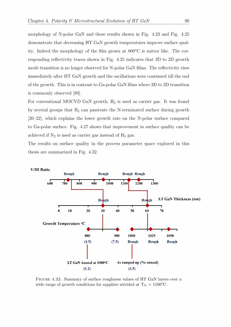
Chapter 4. Polarity & Microstructural Evolution of HT GaN 90
morphology of N-polar GaN and these results shown in Fig. 4.23 and Fig. 4.25
demonstrate that decreasing HT GaN growth temperatures improve surface qual-
ity. Indeed the morphology of the film grown at 800oC is mirror like. The cor-
responding reflectivity traces shown in Fig. 4.25 indicates that 3D to 2D growth
mode transition is no longer observed for N-polar GaN films. The reflectivity rises
immediately after HT GaN growth and the oscillations were continued till the end
of the growth. This is in contrast to Ga-polar GaN films where 3D to 2D transition
is commonly observed [89].
For conventional MOCVD GaN growth, H2 is used as carrier gas. It was found
by several groups that H2 can passivate the N-terminated surface during growth
[20–22], which explains the lower growth rate on the N-polar surface compared
to Ga-polar surface. Fig. 4.27 shows that improvement in surface quality can be
achieved if N2 is used as carrier gas instead of H2 gas.
The results on surface quality in the process parameter space explored in this
thesis are summarized in Fig. 4.32.
Figure 4.32: Summary of surface roughness values of HT GaN layers over awide range of growth conditions for sapphire nitrided at TN = 1100oC.

Chapter 4. Polarity & Microstructural Evolution of HT GaN 91
4.4.2.3 Crystalline quality of HT GaN
The data for crystalline quality is summarized in Fig. 4.33 in the processing
parameter space explored in this thesis.
Figure 4.33: Summary of (0002) x-ray rocking curve FWHM values of HTGaN layers over a wide range of growth conditions for sapphire nitrided at TN
= 1100oC.
For dominantly N-polar GaN containing inversion domains, the crystalline quality
FWHM values would be influenced both by inversion domain density as well as
dislocation density arising out coalescence effects. For given growth temperature
and NL thickness the HRXRD rocking curve FWHM for (0002) and {101̄1} peaks
increases with V/III ratio and for a given V/III ratio and NL thickness, the FWHM
values increase with growth temperature. The increase in FWHM with V/III ratio
can be attributed to the higher hillock density and therefore a higher inversion
domain density. The effect of inversion domain density on FWHM of samples is
also evident in HT GaN grown after an anneal or directly after ramp up. However
since all these conditions have rough surface morphology, these conditions are
not of much interest. Of particular interest the effect of lower HT GaN growth

Chapter 4. Polarity & Microstructural Evolution of HT GaN 92
temperatures at 800 and 900oC. Decreasing the growth temperature substantially
improves the surface quality but increases the FWHM of rocking curves. Assuming
that the FWHM values are affected by LT GaN nucleation density and therefore
the coalescence density as explained in the preceding section, HT GaN was grown
at 800oC after annealing the LT GaN at 1000oC to reduce the LT GaN nucleation
density. A substantial decrease in FWHM is observed as a consequence. Detailed
analysis on the effect of inversion domain density and other defects in N-polar
LT GaN is required to understand fully the effects of growth parameters on the
crystalline quality of HT N-polar LT GaN.
4.5 Summary & conclusions
� A large range of growth parameter space that includes LT GaN thickness,
V/III ratio and growth temperature of HT GaN growth have been explored
for varying nitridation temperatures.
� Low temperature nitridation upto TN = 530oC results in Ga-polar GaN while
nitridation above TN = 530oC results in N-polar GaN.
� Growth parameter conditions have been optimized for both surface quality
and crystalline quality of Ga-polar GaN and the rationale for processing
effects developed.
� Growth parameter conditions have also been arrived at, which allow the re-
alization of device quality N-polar GaN without the necessity of deliberately
miscut sapphire (0001) wafers.

Chapter 5
Summary, Conclusions and
Future Work
We have explored a large domain of growth parameter space including nitrida-
tion temperature, LT GaN nucleation layer control, HT GaN growth with varying
V/III ratios and growth temperature to understand the dependence on these pa-
rameters of polarity and surface and crystalline quality of GaN grown on basal
plane sapphire.
� It has been shown that a modified sapphire (nitrided sapphire) surface plays a
key role in determining the polarity of subsequently grown GaN layers. The
modified surface is characterized by its chemical nature and is controlled
by nitridation temperature (TN). The presence of Al-N bond environment
formed at HT nitridation (TN ≥ 800oC) yields strong c-oriented wurtzite
LT GaN films. In contrast, presence of AlOxN1−x (Al2O3 based structural
motifs) formed at (TN = 530oC) yields (111) oriented cubic LT GaN films in
the as grown stage. The orientation of LT GaN in the subsequent processes is
controlled by the structural transformation of the underlying nitrided layer.
� The polarity of two-step based HT GaN layers grown on such a modified
sapphire surfaces is not the same. N-polar grows preferentially on modified
93

Chapter 5. Summary, Conclusions and Future Work 94
sapphire surface with an Al-N chemical bond environment with AlN struc-
tural motifs, while Ga-polar GaN grows on AlOxN1−x sapphire surfaces. The
former is observed at nitridation temperatures down to TN = 800oC while
the latter is found at nitridation temperatures to TN = 530oC.
� The effect of various growth parameters on HT GaN eipilayers discussed in
this dissertation shows that the surface quality, and mosaicity of HT GaN
layers critically depends upon the process parameters such as growth tem-
perature, V/III ratio, LT GaN growth and annealing time. A domain of
processing was identified for high surface quality Ga-polar GaN with accept-
able crystalline quality, and a rationale for the observed effects has been
presented.
� It was shown that the surface quality of N-polar GaN epitaxial layers grown
on non-miscut sapphire (0001) wafers, strongly depends upon the growth
temperature. The relative amount of O atom content presented in the pre-
cursor nitrided layers is a critical factor to obtain better surface quality of N-
polar GaN base layers and device quality N-polar GaN layers were obtained
for the first time on non-miscut sapphire wafers at low growth temperatures
(TN = 800oC) layers.
Several directions for additional work emerge from the thesis:
� Many observations of the thesis and the proposed rationale have depended
on analysis by techniques such as XPS and HRXRD coupled with SEM and
AFM characterization. Direct evidence of posed structures should be ob-
tained by TEM using recent aberration corrected techniques to elucidate
the details of structure and chemistry of the nanoscale interfaces and pre-
cursor layers that are vital to the quality of the GaN epilayers.
� Similarly details of defect structures in Ga-polar and N-polar epilayers grown
in this work require characterization by TEM to relate these defect structures
to the observed FWHM data obtained in this work.

Chapter 5. Summary, Conclusions and Future Work 95
� A better understanding of the mechanisms underlying the effect of growth
temperature on the quality of N-polar GaN would be desirable.
� The precise origin of polarity remains unknown. The results of this thesis
suggest that the O atom content on AlN based structural motifs of the ni-
trided layer determine the polarity. However the termination of the underly-
ing sapphire at different temperatures and its stable surface structure at any
temperature may play a role. The results of this thesis coupled with TEM
will provide a framework in which ab-initio calculations of stable structure
could be performed to understand the role of these surfaces and interfaces
in determining polarity.
� It has been determined that nitridation temperatures upto TN = 530oC
results in Ga-polarity of HT GaN epilayers while nitridation temperatures
above TN = 800oC result in N-polar GaN epilayers. A more precise definition
in the temperature domains would be useful in terms of device processing.
� As discussed in Sec. 1.3.2 of Chapter 1, there are certain advantages with
the N-polar based HEMT devices when compared to the conventional Ga-
polar GaN based HEMTs. The results of this thesis suggest that it should
be possible to optimize the Al0.25Ga0.75N layer growth on the N-polar GaN
base layers for HEMT device applications.


Appendix A
Specifications of MOCVD
Reactor
System: Aixtron make research scale single wafer Metal Organic Chemical Vapor
deposition (MOCVD).
Model:AIX 200/4 RF.
Type: Double walled water cooled cold wall reactor.
Hot zone: Detachable quartz liner tube with SiC and TaC thermal insulations.
Gas flow mechanism: Horizontal laminar gas flow with group III and group
V species carried in to the growth chamber through separate gas line.
Substrate compatibility: 1 cm2, 2 inch, 3 inch wafers.
Substrate rotation mechanism: Gas foil rotation by lift off mechanism.
Substrate heating mechanism: Radiative RF heating.
97

Appendix A. Appendix A 98
Working temperature range: From above room temperature to 1500oC.
Working pressure range: 10 to 1000 mbar.
Wafer handling: Through dry nitrogen conditioned glove box free from O2 and
H2O below 10 ppm to avoid oxygen incorporation during growth.

Bibliography
[1] Burak Ozpineci, Leon M. Tolbert, S. Kamrul Islam, and Madhu Chinthavali.
Comparison of wide band gap semiconductors for power electronic applica-
tions. doi: http://web.ornl.gov/∼webworks/cppr/y2001/rpt/118817.pdf.
[2] Hadis Markoc. Hand Book of Nitride Semiconductors: Material Properties
and Growth. 1, 2008.
[3] Hadis Markoc. Hand Book of Nitride Semiconductors: GaN based Optical
and Electronic Devices. 1, 2009.
[4] CSM. Compound Semiconductors Magazine, 2013. doi: http://www.
compoundsemiconductor.net/.
[5] S. Raghavan and Joan M. Redwing. Journal of Applied Physics, 98:023514,
2005.
[6] S. Raghavan and Joan M. Redwing. Journal of Applied Physics, 98:023518,
2005.
[7] Weijun Luo, Xiaoliang Wang, Hongling Xiao, Cuimei Wang, Junxue Ran,
Lunchun Guo, Jianping Li, Hongxin Liu, Yanling Chen, Fuhua Yang, and
Jinmin Li. Microelectronics Journal, 39:1108, 2008.
[8] S Raghavan and Joan M. Redwing. III-V Compound Semiconductors: Inte-
gration with Silicon Based Microelectronics, Chapter 5. 2011.
[9] K. Uchida, A. Watanabe, F. Yano, M. Kouguchi, and T. Tanaka. Journal of
Applied Physics, 79:3487, 1996.
99

Bibliography 100
[10] P. Venngus and B. Beaumont. Applied Physics Letters, 75:4115, 1999.
[11] Min Hong Kim, Cheolsoo Sone, Jae Hyung Yi, and Euijoon Yoon. Applied
Physics Letters, 71:1228, 1997.
[12] N. Grandjean, J. Massies, Y. Martinez, P. Veneguess, M. Leroux, and
M. Laugt. Journal of Crystal Growth, 178:220, 1998.
[13] T. Yamaguchi, T. Araki, Y. Saito, K. Kano, H. Kanazawa, Y. Nanishi, N. Ter-
aguchi, and A. Suzuki. Journal of Crystal Growth, 237:993, 2002.
[14] Shunro Fuke, Hidekazu Teshigawara, Kazuhiro Kuwahara, Yasushi Takano,
and Takahiro Ito. Journal of Applied Physics, 83:764, 1998.
[15] H. Amano, N. Sawaki, I. Akasaki, and Y. Toyoda. Applied Physics Letters,
48:353, 1986.
[16] S. Nakamura. Japanese Journal of Applied Physics, 30:L1705, 1991.
[17] Tosja Zywietz, Jorg Neugebauer, and Matthias Scheffler. Applied Physics
Letters, 73:487, 1998.
[18] M. Sumiya, K. Yoshimura, T. Ito, K. Ohtsuka, S. Fuke, K. Mizuno, M. Yoshi-
moto, H. Koinuma, A. Ohtomo, and M. Kawasaki. Journal of Applied Physics,
88:1158, 2000.
[19] Qian Sun, Yong Suk Cho, Bo Hyun Kong, Hyung Koun Cho, Tsung Shine
Ko, Christopher D. Yerino, In-Hwan Lee, and Jung Han. Journal of Crystal
Growth, 311:2948, 2009.
[20] R. Collazo, S. Mita, A. Aleksov, R. Schlesser, and Z. Sitar. Journal of Crystal
Growth, 287:586, 2006.
[21] J. E. Northrup and J. Neugebauer. Applied Physics Letters, 85:3429, 2004.
[22] Xue Wang, Shunfeng Li, Sonke Fundling, Jiandong Wei, Milena Erenburg,
Hergo-H Wehmann, Andreas Waag, Werner Bergbauer, Martin Strassburg,
Uwe Jahn, and Henning Riechert. Journal of Crystal Growth and Design, 12:
2552, 2012.

Bibliography 101
[23] S. Keller, N. A. Fichtenbaum, F. Wu, D. Brown, and A. Rosales. Journal of
Applied Physics, 102:083546, 2007.
[24] S. Nakamura, M. Senoh, N. Iwasa, and S. Nagahama. Japanese Journal of
Applied Physics, 34:L797, 1995.
[25] S. Nakamura, M. Senoh, N. Iwasa, S. Nagahama, T. Yamada, and T. Mukai.
Japanese Journal of Applied Physics, 34:L1332, 1995.
[26] S. Nakamura. Science, 281:956, 1998.
[27] M. Asif Khan, A. Bhattarai, J. N. Kuznia, and D. T. Olson. Applied Physics
Letters, 63:1214, 1993.
[28] Umesh K. Mishra, L. Shen, T. E. Kazior, and Y. F. Wu. Proceedings to IEEE,
96:287, 2008.
[29] A. Chini, R. Coffie, G. Meneghesso, E. Zanoni, D. Buttari, S. Heikman,
S. Keller, and U. K. Mishra. Electronic Letters, 39:625, 2003.
[30] Huili Xing, Y. Dora, A. Chini, S. Heikman, S. Keller, and U. K. Mishra. IEEE
Electronic Device Letters, 25:161, 2004.
[31] Y. F. Wu, M. Moore, A. Saxler, T. Wisleder, and P. Parikh. Proceedings to
IEEE Device Research Conference, page 151, 2006.
[32] O. Ambacher, B. Foutz, J. Smart, J. R. Shealy, N. G. Weimann, K. Chu,
M. Murphy, A. J. Sierakowski, W. J. Schaff, L. F. Eastman, R. Dimitrov,
A. Mitchell, and M. Stutzmann. Journal of Applied Physics, 87:334, 2000.
[33] Man Hoi Wong, Stacia Keller, Nidhi, Sansaptak Dasgupta, Daniel J Den-
ninghoff, Seshadri Kolluri, David F Brown, Jing Lu, Nicholas A Fichten-
baum, Elaheh Ahmadi, Uttam Singisetti, Alessandro Chini, Siddharth Rajan,
Steven P DenBaars, James S Speck, and Umesh K Mishra. Semiconductor
Science and Technology, 28:074009, 2013.
[34] P. S. Park and S. Rajan. IEEE Transactions on Electron Devices, 58:704,
2011.

Bibliography 102
[35] D. Guerra, M. Saraniti, N. Faralli, D. K. Ferry, S. M. Goodnick, and F. A.
Marino. IEEE Transactions on Electron Devices, 57:3348, 2010.
[36] P. S. Park, D. N. Nath, and S. Rajan. IEEE Transactions on Electron Devices,
33:991, 2012.
[37] S. Dasgupta, D. F. Brown, F. Wu, S. Keller, J. S. Speck, and U. K. Mishra.
Applied Physics Letters, 96:143504, 2010.
[38] O. Ambacher, J. Smart, J. R. Shealy, N. G. Weimann, and K. Chu. Journal
of Applied Physics, 85:3222, 1999.
[39] Seshadri Kolluri, Stacia Keller, Steven P. Denbaars, and Umesh K. Mishra.
IEEE Transactions on Electron Devices, 30:584, 2009.
[40] S. Keller, C. S. Suh, Z. Chen, R. Chu, and S. Rajan. Journal of Applied
Physics, 103:033708, 2008.
[41] S.Keller, N.A.Fichtenbaum, M.Furukawa, J.S.Speck, S.P.DenBaars, and
U.K.Mishra. Applied Physics Letters, 90:191908, 2007.
[42] H. P. Maruska and J. Tietjen. Journal of Applied Physics, 72:327, 1969.
[43] Shuji Nakamura and Michael R. Krames. History of GaN Based LEDs for
Illumination. Proceedings of the IEEE, 2013. doi: 10.1109/JPROC.2013.
2274929.
[44] Akinori Koukitu, Naoyuki Takahashi, and Hisashi Seki. Japanese Journal of
Applied Physics, 36:L1136, 1997.
[45] Y. Xi, Th. Gessmann, and E. F. Schubert. Solubility and Dilution of Met-
alorganic Sources.
[46] N. Grandjean, J. Massies, F. Semond, S. Yu. Karpov, and R. A. Talalaev.
Applied Physics Letters, 74:1854, 1999.
[47] D. D. Koleske, A. E. Wickenden, R. L. Henry, J. C. Culbertson, and M. E.
Twigg. Journal of Crystal Growth, 223:466, 2001.

Bibliography 103
[48] B. V. L. Vov. Kinetics and mechanism of thermal decomposition of GaN.
Thermochimica Acta, 360:85, 2000.
[49] Z. A. Munir and A. W. Searcy. Journal of Chemical Physics, 42:4223, 1965.
[50] Ivan V Markov. Crystal growth for beginners. 2003.
[51] D. D. Koleske, A. E. Wickenden, R. L. Henry, W. J. DeSisto, and R. J.
Gorman. Journal of Applied Physics, 84:1998, 1998.
[52] V. Srikant, J. S. Speck, and D. R. Clarke. Journal of Applied Physics, 82:
4286, 1997.
[53] M A Moram and M E Vickers. Reports on Progress in Physics, 72:036502,
2009.
[54] Eric Chason. Use of kSA MOS system for stress and thickness monitoring
during CVD growth . 2000.
[55] H. Amano, I Akasaki, K. Hiramatsu, N. Koide, and N. Sawaki. Thin Solid
Films, 163:415, 1988.
[56] M. Sumiya, M. Tanaka, K. Ohtsuka, S. Fuke, T. Ohnishi, I. Ohkubo,
M. Yoshimoto, H. Koinuma, and M. Kawasaki. Applied Physics Letters, 75:
674, 1999.
[57] M. Sumiya, N. Ogusu, Y. Yotsuda, M. Itoh, S. Fuke, T. Nakamura,
S. Mochizuki, T. Sano, S. Kamiyama, H. Amano, and I. Akasaki. Journal of
Applied Physics, 93:1311, 2003.
[58] F. Dwikusuma and T. F. Keuch. Journal of Applied Physics, 94:5656, 2003.
[59] Tadao Hashimoto, Yoshitami Terakoshi, Masaaki Yuri, Masahiro Ishida, Os-
amu Imafuji, Takashi Sugino, and Kunio Itoh. Journal of Applied Physics,
86:3670, 1999.
[60] J. Narayan, Punam Pant, A. Chug, H. Choi, and J. C. C. Fan. Journal of
Applied Physics, 99:054313, 2006.

Bibliography 104
[61] N. Grandjean, J. Massies, and M. Leroux. Applied Physics Letters, 69:2071,
1996.
[62] J. Chen, S. M. Zhang, B. S. Zhang, J. J. Zhu, G. Feng, X. M. Shen, Y. T.
Wang, H. Yang, and W. C. Zheng. Journal of Crystal Growth, 254:348, 2003.
[63] Ki Soo Kim, Chang Seok Oh, Kang Jea Lee, Gye Mo Yang, Chang Hee Hong,
Kee Young Lim, and Hyung Jae Lee. Journal of Applied Physics, 84:8441,
1999.
[64] Dong Sing Wuu, Ray Hua Horng, Wei Hao Tseng, Wei Tsung Lin, and
Chung Yuan Kung. Journal of Crystal Growth, 220:235, 2000.
[65] D. Kapolnek, X. H. Wu, B. Heying, S. Keller, B. P. Keller, U. K. Mishra,
S. P. DenBaars, and J. S. Speck. Applied Physics Letters, 67:1541, 1995.
[66] L. Sugiura, K. Itaya, J. Nishio, H. Fujimoto, and Y. Kokubun. Journal of
Applied Physics, 82:4877, 1997.
[67] M. A. Mastro, O. M. Kryliouk, M. D. Reed, T. J. Anderson, A. Davydov,
and A. Shapiro. physica status solidi (a), 188:467, 2001.
[68] T. Yang, K. Uchida, T. Mishima, J. Kasai, and J. Gotoh. physica status solidi
(a), 180:45, 2000.
[69] T. Wang, T. Shirahama, H. B. Sun, H. X. Wang, J. Bai, and S. Sakai. Applied
Physics Letters, 76:2220, 2000.
[70] Yuval Golan, Paul Fini, Steven P. Denbaars, and James S. Speck. Japanese
Journal of Applied Physics, 37:4695, 1998.
[71] Leland Rosenberger, Ronald Baird, McCullen Erik, Gregory Auner, and Gina
Shreve. Surface and Interface Analysis, 40:1254, 2008.
[72] M. Losurdo, P. Capezzuto, and G. Bruno. Journal of Applied Physics, 88:
2138, 2000.
[73] J. Ohta, H. Fujioka, M. Oshima, K. Fujiwara, and A. Ishii. Applied Physics
Letters, 83:3075, 2003.

Bibliography 105
[74] H. M. Liao, R. N. S. Sodhi, and T. W. Coyle. Journal of Vacuum Science &
Technology A, 11:2681, 1993.
[75] Tadao Hashimoto, Yoshitami Terakoshi, Masahiro Ishida, Masaaki Yuri, Os-
amu Imafuji, Takashi Sugino, Akio Yoshikawa, and Kunio Itoh. Journal of
Crystal Growth, 189/190:254, 1998.
[76] A. D. Katnani and K. I. Papathomas. Journal of Vacuum Science & Tech-
nology A, 5:1335, 1987.
[77] Jong Sik Paek, Kyoung Kook Kim, Ji Myon Lee, Dong Joon Kim, Min Su
Yi, Do Young Noh, Hyo Gun Kim, and Seong Ju Park. Journal of Crystal
Growth, 200:55, 1999.
[78] Yasutaka Saito, Toru Akiyama, Kohji Nakamura, and Tomonori Ito. Journal
of Crystal Growth, 362:29, 2013.
[79] D. D. Koleske, M. E. Coltrin, K. C. Cross, C. C. Mitchell, and A. A. Allerman.
Journal of Crystal Growth, 273:86, 2004.
[80] J. Han, T. B. Ng, R. M. Biefeld, M. H. Crawford, and D. M. Follstaedt.
Applied Physics Letters, 71:3114, 1997.
[81] T. H. Myers, L. S. Hirsch, L. T. Romano, and M. R. Richards-Babb. Journal
of Vacuum Science & Technology B, 86:2261, 1998.
[82] L. T. Romano and T. H. Myers. Applied Physics Letters, 71:3486, 1997.
[83] J.L. Weyher, P.D. Brown, A.R.A. Zauner, S.Muller, C.B. Boothroyd, D.T.
Foord, P.R. Hageman, C.J. Humphreys, P.K. Larsen, I. Grzegory, and
S. Porowski. Journal of Crystal Growth, 204:419, 1999.
[84] L. T. Romano, J. E. Northrup, and M. A. Okeefe. Applied Physics Letters,
69:2394, 1996.
[85] Younghun Jung, Jaehui Ahn, K H Baik, Donghwan Kim, Stephen J. Pearton,
Fan Ren, and Jihyun Kim. Journal of Electro Chemical Society, 159:H117,
2012.

Bibliography 106
[86] G. Moldovan, M. J. Roe, I. Harrison, M. Kappers, C. J. Humphreys, and
P. D. Brown. Philosophical Magzine, 86:2315, 2006.
[87] Dongsheng Li, M. Sumiya, S. Fuke, Deren Yang, Duanlin Que, Y. Suzuki,
and Y. Fukuda. Journal of Applied Physics, 90:4219, 2001.
[88] D. A. Stocker, E. F. Schubert, and J. M. Redwing. Applied Physics Letters,
73:2654, 1998.
[89] Qian Sun, Y. S. Cho, I. H. Lee, J. Han, and B. H. Kong. Applied Physics
Letters, 93:131912, 2008.
[90] Sunwoon Kim, Jeongtak Oh, Joongseo Kang, Dongjoon Kim, Jonghak Won,
Je Won Kim, and Hyung-Koun Cho. Journal of Crystal Growth, 262:7, 2004.
[91] S. E. Bennett. Materials Science and Technology, 26:1017, 2010.
[92] P. Vennegues, B. Beaumont, S. Haffouz, M. Vaille, and P. Gibart. Journal of
Crystal Growth, 187:167, 1998.
[93] H. M. Ng, D. Doppalapudi, T. D. Moustakas, N. G. Weimann, and L. F.
Eastman. Applied Physics Letters, 73:821, 1998.