effects of annealing conditions on optical and electrical...
TRANSCRIPT
JOURNAL OF APPLIED PHYSICS VOLUME 89, NUMBER 6 15 MARCH 2001
Effects of annealing conditions on optical and electrical characteristicsof titanium dioxide films deposited by electron beam evaporation
V. Mikhelashvili and G. Eisensteina)
Electrical Engineering Department, Technion, Haifa, 32000, Israel
~Received 10 November 2000; accepted for publication 20 December 2000!
We report measured evolutions of the optical band gap, refractive index, and relative dielectricconstant of TiO2 film obtained by electron beam gun evaporation and annealed in an oxygenenvironment. A negative shift of the flat band voltage with increasing annealing temperatures, forany film thickness, is observed. A dramatic reduction of the leakage current by about four orders ofmagnitude to 531026 A/cm2 ~at 1 MV/cm! after 700 °C and 60 min annealing is found for filmsthinner than 15 nm. An equivalent SiO2 thickness of the order of 3–3.5 nm is demonstrated. Anapproach is presented to establish that at different ranges of applied voltage the hopping, spacecharge limited current, and Fowler–Nordheim are the basic mechanisms of carrier transport into theTiO2 film. © 2001 American Institute of Physics.@DOI: 10.1063/1.1349860#
m
o. A
li
reona
n
ib
eicTurrm
udnde
s
fore
sivegepo-sedgeas
de-gov-enton-
un-ilica
t al-
0–
2g-e
ned
byiedures
e–
I. INTRODUCTION
The use of high dielectric constant~e! materials in smallscale metal–insulator–semiconductor~MIS! devices hasbeen considered in numerous recent publications. Theseterials enable to maintain the capacitance density of thin~lessthan 5 nm thick! SiO2 films while providing low leakagecurrents. Examples of such materials include, Y2O3,Ta2O5,
1–9 and TiO2 which has the higheste value.10 Roomtemperature grown TiO2 can have three structural forms: twcrystalline, anatase and rutile, and an amorphous phasenealing at temperatures between 350 and;800 °C initiates atransition from primary anatase to the rutile phase.11–13
The relative dielectric constant of TiO2 depends on thecrystalline form and changes from;31 to 60–100, for crys-talline anatase and rutile respectively.10,14 Some structuraland optical characteristics of TiO2 obtained by the sol–gemethod and by oxidation of sputtered Ti were describedRefs. 15 and 16. Electrical characteristics of MIS structuwith a TiO2 insulator deposited by chemical vapor depositimethod and postannealed in oxygen or oxygen/hydrogenbient have been studied and reported.17–24 Composite filmsof Ta2O5:TiO2 used to enhance the relative dielectric costant and lower leakages were also investigated.25–27
This article contains two related parts. First, we descrdetailed optical and electrical characterizations of TiO2 filmsobtained by electron beam gun evaporation. We present msurements of absorption spectra, refractive index and thness, relative dielectric constant, and charge transport.dielectric properties in field effect devices, the leakage crent, and the interface properties are closely related to catrapping processes as well as defects, composition, andcrostructure aspects of the thin films. In the systematic stpresented here, we emphasize therefore dependencies onealing conditions, film thickness, and morphology. Suchtailed understanding of the film properties are imperativeTiO2 is to be developed to a degree which will enable its u
a!Electronic mail: [email protected]
3250021-8979/2001/89(6)/3256/14/$18.00
Downloaded 08 Oct 2003 to 132.68.1.29. Redistribution subject to AIP
a-
n-
ns
m-
-
e
a-k-her-ier
i-yan--
ife
in silicon devices. Detailed data of TiO2 films obtained byelectron beam gun evaporation has not been reported bealthough some results concerning single layer TiO2
28 anddouble layer TiO2/Ta2O5
29 or TiO2/Y2O330 systems have
been published.The second part of the article presents a comprehen
procedure for analyzing current density versus volta(J–V) characteristics based on analysis of the power exnent parameter. This general procedure, which can be ufor any dielectric thin film, serves to determine the chartransport nature under different bias conditions as wellvarious aspects that limit metal–oxide–semiconductorvice performance. For each charge transport mechanismerning the behavior in a respective bias regime we presgeneral formalisms and use our experimental results to cfirm it.
II. EXPERIMENTAL PROCEDURE
P-type Si wafers~100! with resistivity of 8–10V cmwere used to prepare the MIS structures. TiO2 films withthickness in the range of 15–130 nm were deposited onheated Si substrates without additional oxygen. Fused swas used as a substrate for 153 nm thick TiO2 film for theoptical measurement. The deposition was carried out apressure of (2 – 3)31026 Torr and a rate of 0.05 nm/s. Folowing the deposition, the films were annealed in an O2 en-vironment at several temperatures in the range of 35750 °C and for different times up to 120 min.
MIS capacitor structures with different areas (31025– 331024 cm2) were patterned using standard lithoraphy. The top contact was Al/Ti while Al was used for thback contact. The deposited film thickness was determifrom step height measurements bya-step stylus profilometerand ellipsometry. The refractive index was also measuredellipsometry. The optical absorption of the films was studat a wavelength range of 250–900 nm. The surface featwere examined by an atomic force microscope~AFM! oper-ating in the tapping mode. High frequency capacitanc
6 © 2001 American Institute of Physics
license or copyright, see http://ojps.aip.org/japo/japcr.jsp
aer
iOeng.
wecopre
ry
edd
ed
ses
rt
toin
titve
re-
in
t of
an-themida-
ough-est
ssnic
ith
e
pera-
3257J. Appl. Phys., Vol. 89, No. 6, 15 March 2001 V. Mikhelashvili and G. Eisenstein
voltage (C–V) and current density–voltage (J–V) measure-ments were performed using standard techniquesinstruments. All electrical and optical measurements wcarried out at room temperature.
III. RESULTS
A. Optical properties
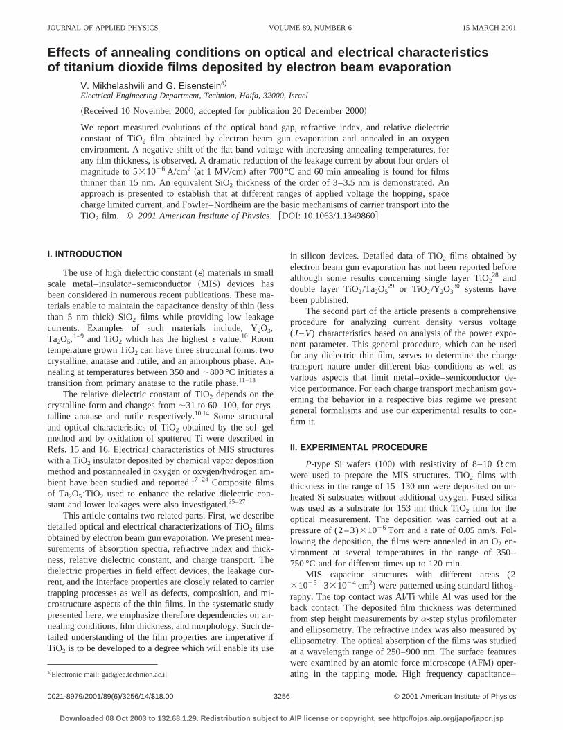
Room temperature optical absorption spectra of T2films: as deposited and after a 60 min anneal at differtemperatures in an oxygen environment are shown in Fias aabs
1/2 versus photon energy (hn). The absorption coeffi-cient above the threshold of fundamental absorption follothe (hn2Eg)2 energy dependence corresponding to indirtransitions with absorption or emission of phonons. Thetical band gap (Eg) values near the absorption edge weextrapolated~see for example the dash line along curve 4! forthe as deposited~amorphous state, curve 1!, partially or fullcrystallized films ~curves 2 to 4, respectively!, and werefound to be in the range of 3.12–3.25 eV. TheEg values ofthe annealed films are close to those reported for polyctalline anatase and rutile films~3.2 and 3.05 eV,respectively!.10 However, they are lower than those obtainfor an anatase of single crystal31 and for reactive sputtereTiO2 film.13
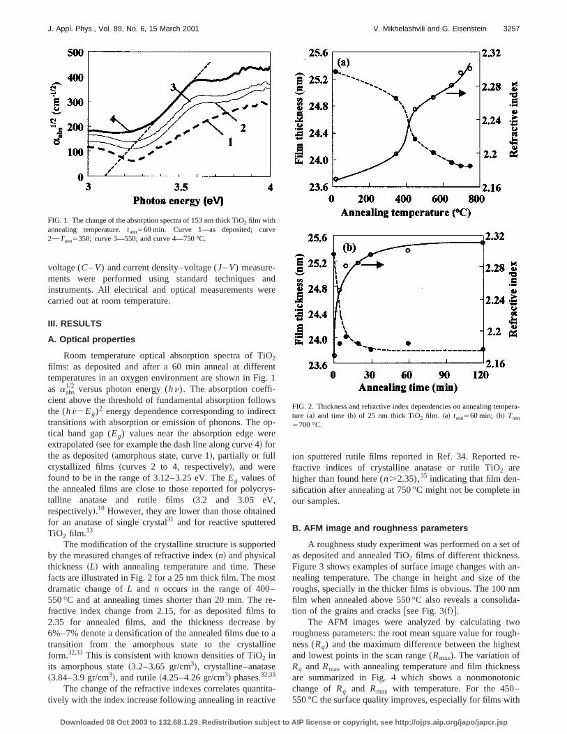
The modification of the crystalline structure is supportby the measured changes of refractive index~n! and physicalthickness~L! with annealing temperature and time. Thefacts are illustrated in Fig. 2 for a 25 nm thick film. The modramatic change ofL and n occurs in the range of 400–550 °C and at annealing times shorter than 20 min. Thefractive index change from 2.15, for as deposited films2.35 for annealed films, and the thickness decrease6%–7% denote a densification of the annealed films duetransition from the amorphous state to the crystallform.32,33 This is consistent with known densities of TiO2 inits amorphous state~3.2–3.65 gr/cm3!, crystalline–anatase~3.84–3.9 gr/cm3!, and rutile~4.25–4.26 gr/cm3! phases.32,33
The change of the refractive indexes correlates quantively with the index increase following annealing in reacti
FIG. 1. The change of the absorption spectra of 153 nm thick TiO2 film withannealing temperature.tann560 min. Curve 1—as deposited; curv2—Tann5350; curve 3—550; and curve 4—750 °C.
Downloaded 08 Oct 2003 to 132.68.1.29. Redistribution subject to AIP
nde
t1
st-
s-
t
e-obya
e
a-
ion sputtered rutile films reported in Ref. 34. Reportedfractive indices of crystalline anatase or rutile TiO2 arehigher than found here (n.2.35),35 indicating that film den-sification after annealing at 750 °C might not be completeour samples.
B. AFM image and roughness parameters
A roughness study experiment was performed on a seas deposited and annealed TiO2 films of different thickness.Figure 3 shows examples of surface image changes withnealing temperature. The change in height and size ofroughs, specially in the thicker films is obvious. The 100 nfilm when annealed above 550 °C also reveals a consoltion of the grains and cracks@see Fig. 3~f!#.
The AFM images were analyzed by calculating twroughness parameters: the root mean square value for roness (Rq) and the maximum difference between the highand lowest points in the scan range (Rmax). The variation ofRq and Rmax with annealing temperature and film thickneare summarized in Fig. 4 which shows a nonmonotochange ofRq and Rmax with temperature. For the 450–550 °C the surface quality improves, especially for films w
FIG. 2. Thickness and refractive index dependencies on annealing temture ~a! and time~b! of 25 nm thick TiO2 film. ~a! tann560 min; ~b! Tann
5700 °C.
license or copyright, see http://ojps.aip.org/japo/japcr.jsp

3258 J. Appl. Phys., Vol. 89, No. 6, 15 March 2001 V. Mikhelashvili and G. Eisenstein
FIG. 3. AFM images of as deposited~a!, ~c!, and ~e! and annealed~b!, ~d!, and ~f! TiO2 films of various thickness.~a!, ~b!—L515 nm; ~c!, ~d!—L525 nm; ~e!, ~f!—L5100 nm. tann560 min; Tann5700 °C.
e
nsuin
sio
crys-
5t
thickness of less than 50 nm. At an annealing temperatur550 °C the values ofRq and Rmax, of films thinner than 50nm, decrease respectively to 0.1–0.15 nm and 1–1.5values which are comparable with the silicon substrateface. At temperatures above 550 °C a relatively sharpcrease of bothRq andRmax is observed for all thickness. Thiis generally attributed to relaxation of the thermal expans
Downloaded 08 Oct 2003 to 132.68.1.29. Redistribution subject to AIP
of
m,r--
n
mismatch stresses between the silicon substrate and thetallized TiO2 film.
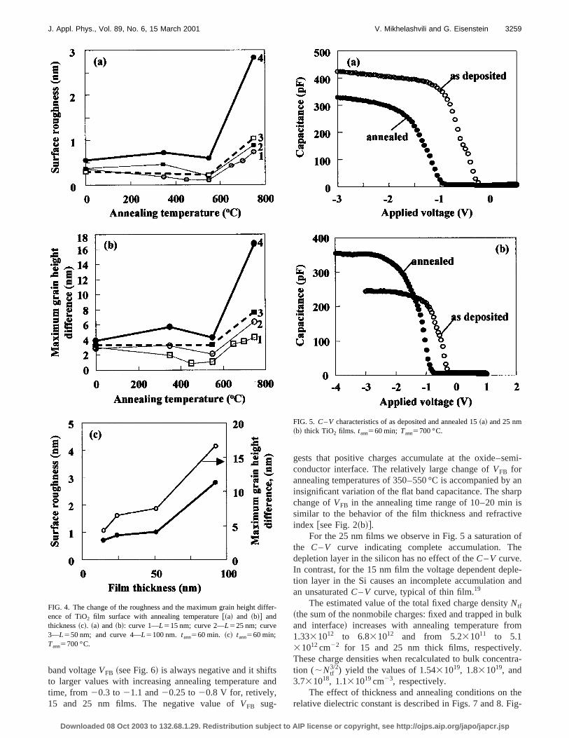
C. Electrical characteristics1. C – V dependence
Typical C–V characteristics of MIS structure with 1and 25 nm thick TiO2 films are shown in Fig. 5. The fla
license or copyright, see http://ojps.aip.org/japo/japcr.jsp
san
emi-
y anarpisve
e
le-and
ulkm
.ntra-
theig-
iffe
3259J. Appl. Phys., Vol. 89, No. 6, 15 March 2001 V. Mikhelashvili and G. Eisenstein
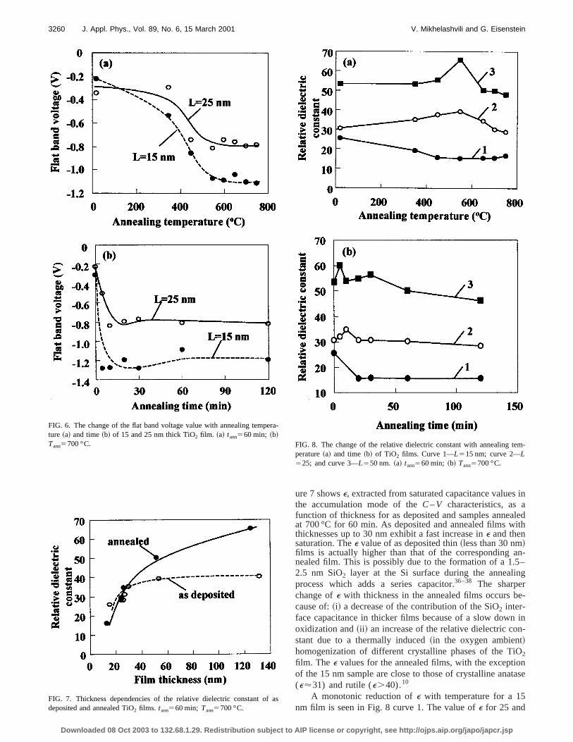
band voltageVFB ~see Fig. 6! is always negative and it shiftto larger values with increasing annealing temperaturetime, from20.3 to21.1 and20.25 to20.8 V for, retively,15 and 25 nm films. The negative value ofVFB sug-
FIG. 4. The change of the roughness and the maximum grain height dence of TiO2 film surface with annealing temperature@~a! and ~b!# andthickness~c!. ~a! and ~b!: curve 1—L515 nm; curve 2—L525 nm; curve3—L550 nm; and curve 4—L5100 nm. tann560 min. ~c! tann560 min;Tann5700 °C.
Downloaded 08 Oct 2003 to 132.68.1.29. Redistribution subject to AIP
d
gests that positive charges accumulate at the oxide–sconductor interface. The relatively large change ofVFB forannealing temperatures of 350–550 °C is accompanied binsignificant variation of the flat band capacitance. The shchange ofVFB in the annealing time range of 10–20 minsimilar to the behavior of the film thickness and refractiindex @see Fig. 2~b!#.
For the 25 nm films we observe in Fig. 5 a saturation ofthe C–V curve indicating complete accumulation. Thdepletion layer in the silicon has no effect of theC–V curve.In contrast, for the 15 nm film the voltage dependent deption layer in the Si causes an incomplete accumulationan unsaturatedC–V curve, typical of thin film.19
The estimated value of the total fixed charge densityNtf
~the sum of the nonmobile charges: fixed and trapped in band interface! increases with annealing temperature fro1.3331012 to 6.831012 and from 5.231011 to 5.131012cm22 for 15 and 25 nm thick films, respectivelyThese charge densities when recalculated to bulk concetion (;Ntf
3/2) yield the values of 1.5431019, 1.831019, and3.731018, 1.131019cm23, respectively.
The effect of thickness and annealing conditions onrelative dielectric constant is described in Figs. 7 and 8. F
r-
FIG. 5. C–V characteristics of as deposited and annealed 15~a! and 25 nm~b! thick TiO2 films. tann560 min; Tann5700 °C.
license or copyright, see http://ojps.aip.org/japo/japcr.jsp
in
aledith
n-–
ng
e-
inn-
Oontase
er
f
em-
3260 J. Appl. Phys., Vol. 89, No. 6, 15 March 2001 V. Mikhelashvili and G. Eisenstein
FIG. 6. The change of the flat band voltage value with annealing tempture ~a! and time~b! of 15 and 25 nm thick TiO2 film. ~a! tann560 min; ~b!Tann5700 °C.
FIG. 7. Thickness dependencies of the relative dielectric constant odeposited and annealed TiO2 films. tann560 min; Tann5700 °C.
Downloaded 08 Oct 2003 to 132.68.1.29. Redistribution subject to AIP
ure 7 showse, extracted from saturated capacitance valuesthe accumulation mode of theC–V characteristics, as afunction of thickness for as deposited and samples anneat 700 °C for 60 min. As deposited and annealed films wthicknesses up to 30 nm exhibit a fast increase ine and thensaturation. Thee value of as deposited thin~less than 30 nm!films is actually higher than that of the corresponding anealed film. This is possibly due to the formation of a 1.52.5 nm SiO2 layer at the Si surface during the annealiprocess which adds a series capacitor.36–38 The sharperchange ofe with thickness in the annealed films occurs bcause of:~i! a decrease of the contribution of the SiO2 inter-face capacitance in thicker films because of a slow downoxidization and~ii ! an increase of the relative dielectric costant due to a thermally induced~in the oxygen ambient!homogenization of different crystalline phases of the Ti2
film. The e values for the annealed films, with the exceptiof the 15 nm sample are close to those of crystalline ana(e'31) and rutile (e.40).10
A monotonic reduction ofe with temperature for a 15nm film is seen in Fig. 8 curve 1. The value ofe for 25 and
a-
as
FIG. 8. The change of the relative dielectric constant with annealing tperature~a! and time~b! of TiO2 films. Curve 1—L515 nm; curve 2—L525; and curve 3—L550 nm. ~a! tann560 min; ~b! Tann5700 °C.
license or copyright, see http://ojps.aip.org/japo/japcr.jsp

T
acuthh
thpgh
aobesiOta
de--ra-
hen
indis-
ofthere-imentu-
er,
ticsentysi-
esatee-
smna-ction
forick
rgep-ses
har-cu-n
asas
3261J. Appl. Phys., Vol. 89, No. 6, 15 March 2001 V. Mikhelashvili and G. Eisenstein
50 nm films ~curves 2 and 3 in Fig. 8, respectively! goesthrough a maximum and starts to decrease above 550 °C.critical value of the annealing time@see Fig. 8~b!# is almostthe same for all thickness, 10–20 min. The reduction ofe forfilms thicker than 20 nm is partially due to the growth ofSiO2 interfacial layer. A second reason is an incorrect callation of the capacitance which comes about due toroughness enhancement in those films when annealed attemperatures~above 550 °C! ~see Figs. 3 and 4!. This leadsto a decrease of the contact area in comparison withpatterned geometrical size as the inner surface of the deited metallic layer is contacting only the tops of the roufilm areas.
2. J – V dependence and current flow mechanisms
TheJ–V curves of Al/Ti/TiO2/Si/Al structures with twodifferent dielectric thickness, negatively biased to set thecumulation mode, are shown in Fig. 9. Three importantservations can be made:~i! the leakage current decreasconsiderably at all applied fields when the amorphous T2
films are annealed at temperatures higher than the cryszation temperature, namely, above 350 °C,~ii ! the reduction
FIG. 9. Current density–voltage characteristics of 15~a! and 25 nm~b!thick TiO2 films. tann560 min; Tann5700 °C.
Downloaded 08 Oct 2003 to 132.68.1.29. Redistribution subject to AIP
he
-eigh
eos-
c--
lli-
of the leakage current density with annealing conditionspends on the film thickness and~iii ! the shift towards negative voltages of the inflection point as the annealing tempeture increases is larger for the thinner film as seen wcomparing Figs. 9~a! and 9~b!.
Several carrier transport mechanisms of charge flowMIS structures biased in the accumulation mode arecussed in Ref. 39. These include double injection, hoppingthe carriers into trapping levels, thermionic emission overbarriers, and field ionization of trapping levels based on,spectively, Schottky, Poole–Frenkel, and Fowler–Nordhetunneling through insulator and space charge limited curr~SCLC!. Determination of the dominant mechanism is usally achieved by graphical linearization of theJ–V depen-dencies in accordance with theoretical formalisms. Howevthe semi- or double logarithmic representation ofJ–V char-acteristics averages over peculiarities of the characteriswhich leads in turn to inaccurate conclusions about currtransport mechanisms and wrong determination of the phcal parameters.The analysis we present uses the power exponent
a5d@ ln~J!#
d@ ln~V!#, ~1!
which describes the voltage dependent slope of theJ–Vcharacteristic in log–log scale.7,40–45
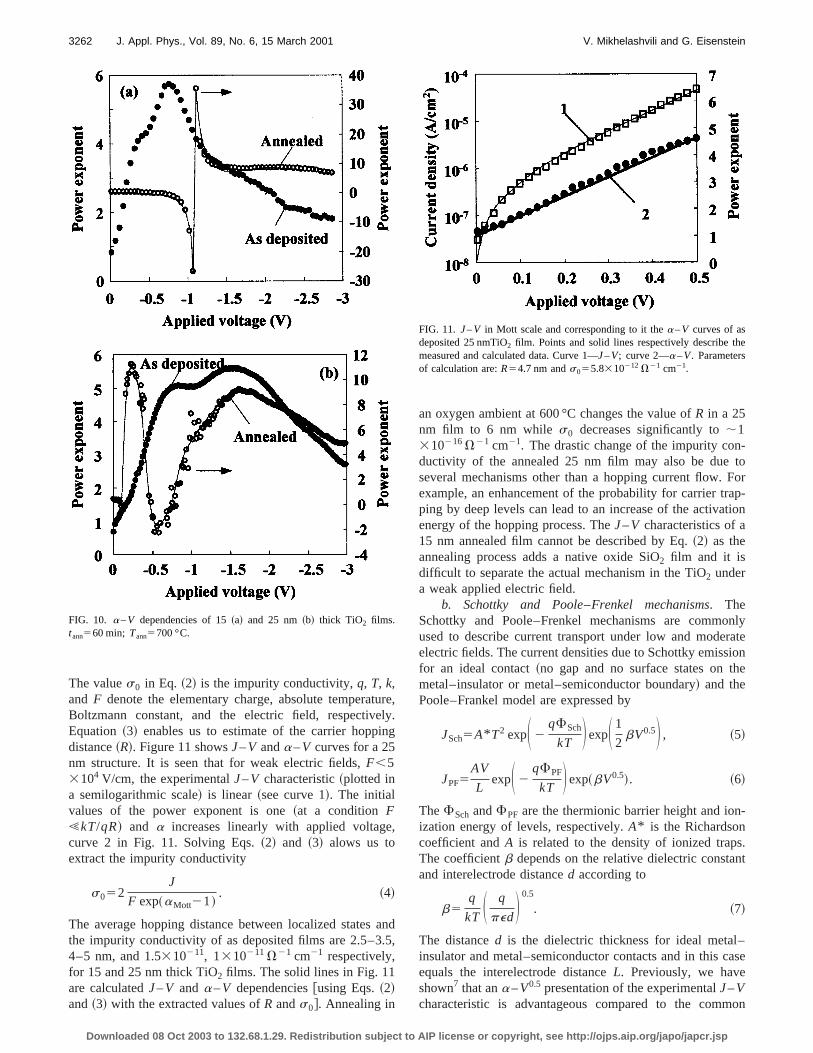
The transformation of the experimentalJ–V dependen-cies of Fig. 9 to thea –V domain, using Eq.~1! is shown inFig. 10. Thea –V characteristic is more sensitive to changtaking place as different current flow mechanisms dominin different ranges of applied voltage. The revelation of pculiar regions~extrema, bends, or asymptotes! on thea –Vcurves and their relation to known mathematical formaliof different current transport processes alows a discrimition among the mechanisms as well as an accurate extraof some physical parameters. This is demonstrated belowthe MIS structures we fabricated with 15 and 25 nm thTiO2 films.
3. Low and moderate electric field range
a. The hopping mechanism: In dielectric materials withextremely low densities of thermally generated free chacarriers and correspondingly low carrier mobilities, the hoping conduction becomes probable. This process that uincoherent jumps of carriers between isolated states is cacterized by the formation of a small polaron at each ocpied site.46,47 Experimental evidence of the polaron driveconductivity in rutile type single-crystal TiO2 is given in Ref.48.
We find that the carrier flow at low voltages throughdeposited TiO2 films as well as postannealed 25 nm films ha hopping nature described by46
JMott51
2s0F expS qFR
kT D , ~2!
or using Eqs.~1! and ~2!
aMott511qFR
kT. ~3!
license or copyright, see http://ojps.aip.org/japo/japcr.jsp
tuly
ing
,
a.5
-toForap-tion
nlyrateionhe
-
s.nt
–ase
mon
he
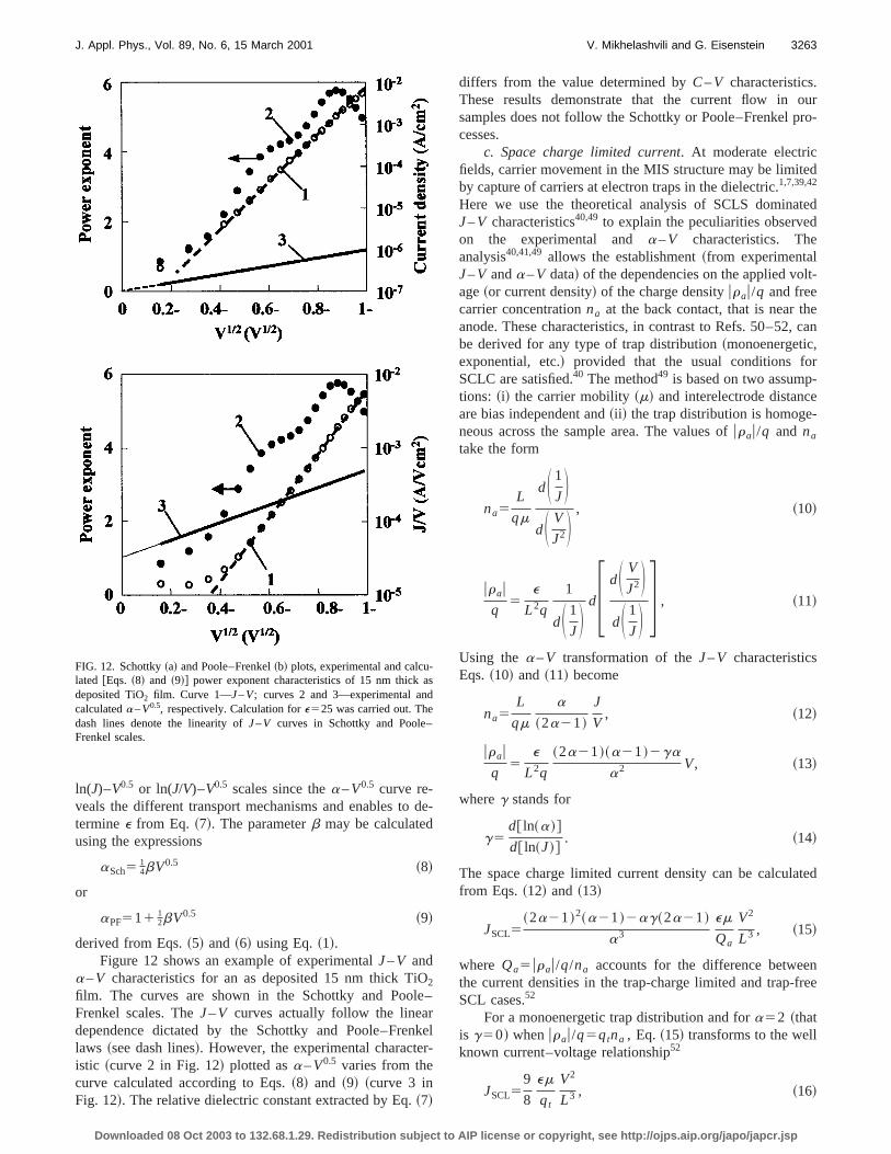
3262 J. Appl. Phys., Vol. 89, No. 6, 15 March 2001 V. Mikhelashvili and G. Eisenstein
The values0 in Eq. ~2! is the impurity conductivity,q, T, k,and F denote the elementary charge, absolute temperaBoltzmann constant, and the electric field, respectiveEquation~3! enables us to estimate of the carrier hoppdistance~R!. Figure 11 showsJ–V anda –V curves for a 25nm structure. It is seen that for weak electric fields,F,53104 V/cm, the experimentalJ–V characteristic~plotted ina semilogarithmic scale! is linear ~see curve 1!. The initialvalues of the power exponent is one~at a conditionF!kT/qR! and a increases linearly with applied voltagecurve 2 in Fig. 11. Solving Eqs.~2! and ~3! alows us toextract the impurity conductivity
s052J
F exp~aMott21!. ~4!
The average hopping distance between localized statesthe impurity conductivity of as deposited films are 2.5–34–5 nm, and 1.5310211, 1310211V21 cm21 respectively,for 15 and 25 nm thick TiO2 films. The solid lines in Fig. 11are calculatedJ–V and a –V dependencies@using Eqs.~2!and~3! with the extracted values ofR ands0#. Annealing in
FIG. 10. a –V dependencies of 15~a! and 25 nm~b! thick TiO2 films.tann560 min; Tann5700 °C.
Downloaded 08 Oct 2003 to 132.68.1.29. Redistribution subject to AIP
re,.
nd,
an oxygen ambient at 600 °C changes the value ofR in a 25nm film to 6 nm while s0 decreases significantly to;1310216V21 cm21. The drastic change of the impurity conductivity of the annealed 25 nm film may also be dueseveral mechanisms other than a hopping current flow.example, an enhancement of the probability for carrier trping by deep levels can lead to an increase of the activaenergy of the hopping process. TheJ–V characteristics of a15 nm annealed film cannot be described by Eq.~2! as theannealing process adds a native oxide SiO2 film and it isdifficult to separate the actual mechanism in the TiO2 undera weak applied electric field.
b. Schottky and Poole–Frenkel mechanisms. TheSchottky and Poole–Frenkel mechanisms are commoused to describe current transport under low and modeelectric fields. The current densities due to Schottky emissfor an ideal contact~no gap and no surface states on tmetal–insulator or metal–semiconductor boundary! and thePoole–Frankel model are expressed by
JSch5A* T2 expS 2qFSch
kT DexpS 1
2bV0.5D , ~5!
JPF5AV
LexpS 2
qFPF
kT Dexp~bV0.5!. ~6!
TheFSch andFPF are the thermionic barrier height and ionization energy of levels, respectively.A* is the Richardsoncoefficient andA is related to the density of ionized trapThe coefficientb depends on the relative dielectric constaand interelectrode distanced according to
b5q
kT S q
pedD 0.5
. ~7!
The distanced is the dielectric thickness for ideal metalinsulator and metal–semiconductor contacts and in this cequals the interelectrode distanceL. Previously, we haveshown7 that ana –V0.5 presentation of the experimentalJ–Vcharacteristic is advantageous compared to the com
FIG. 11. J–V in Mott scale and corresponding to it thea –V curves of asdeposited 25 nmTiO2 film. Points and solid lines respectively describe tmeasured and calculated data. Curve 1—J–V; curve 2—a –V. Parametersof calculation are:R54.7 nm ands055.8310212 V21 cm21.
license or copyright, see http://ojps.aip.org/japo/japcr.jsp
d
Olernkr-
ourro-
ed
tedd
lt-
ecan
r-e-
ted
nree
-asd
3263J. Appl. Phys., Vol. 89, No. 6, 15 March 2001 V. Mikhelashvili and G. Eisenstein
ln(J)–V0.5 or ln(J/V)–V0.5 scales since thea –V0.5 curve re-veals the different transport mechanisms and enables toterminee from Eq. ~7!. The parameterb may be calculatedusing the expressions
aSch514bV0.5 ~8!
or
aPF511 12bV0.5 ~9!
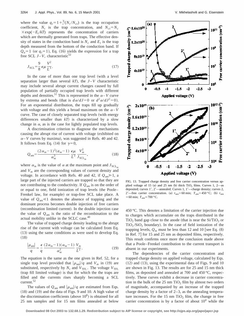
derived from Eqs.~5! and ~6! using Eq.~1!.Figure 12 shows an example of experimentalJ–V and
a –V characteristics for an as deposited 15 nm thick Ti2
film. The curves are shown in the Schottky and PooFrenkel scales. TheJ–V curves actually follow the lineadependence dictated by the Schottky and Poole–Frelaws ~see dash lines!. However, the experimental characteistic ~curve 2 in Fig. 12! plotted asa –V0.5 varies from thecurve calculated according to Eqs.~8! and ~9! ~curve 3 inFig. 12!. The relative dielectric constant extracted by Eq.~7!
FIG. 12. Schottky~a! and Poole–Frenkel~b! plots, experimental and calculated @Eqs. ~8! and ~9!# power exponent characteristics of 15 nm thickdeposited TiO2 film. Curve 1—J–V; curves 2 and 3—experimental ancalculateda –V0.5, respectively. Calculation fore525 was carried out. Thedash lines denote the linearity ofJ–V curves in Schottky and Poole–Frenkel scales.
Downloaded 08 Oct 2003 to 132.68.1.29. Redistribution subject to AIP
e-
–
el
differs from the value determined byC–V characteristics.These results demonstrate that the current flow insamples does not follow the Schottky or Poole–Frenkel pcesses.
c. Space charge limited current. At moderate electricfields, carrier movement in the MIS structure may be limitby capture of carriers at electron traps in the dielectric.1,7,39,42
Here we use the theoretical analysis of SCLS dominaJ–V characteristics40,49 to explain the peculiarities observeon the experimental anda –V characteristics. Theanalysis40,41,49 allows the establishment~from experimentalJ–V anda –V data! of the dependencies on the applied voage~or current density! of the charge densityurau/q and freecarrier concentrationna at the back contact, that is near thanode. These characteristics, in contrast to Refs. 50–52,be derived for any type of trap distribution~monoenergetic,exponential, etc.! provided that the usual conditions foSCLC are satisfied.40 The method49 is based on two assumptions: ~i! the carrier mobility~m! and interelectrode distancare bias independent and~ii ! the trap distribution is homogeneous across the sample area. The values ofurau/q and na
take the form
na5L
qm
dS 1
JDdS V
J2D , ~10!
urauq
5e
L2q
1
dS 1
JD dF dS V
J2DdS 1
JD G , ~11!
Using thea –V transformation of theJ–V characteristicsEqs.~10! and ~11! become
na5L
qm
a
~2a21!
J
V, ~12!
urauq
5e
L2q
~2a21!~a21!2ga
a2 V, ~13!
whereg stands for
g5d@ ln~a!#
d@ ln~J!#. ~14!
The space charge limited current density can be calculafrom Eqs.~12! and ~13!
JSCL5~2a21!2~a21!2ag~2a21!
a3
em
Qa
V2
L3 , ~15!
where Qa5urau/q/na accounts for the difference betweethe current densities in the trap-charge limited and trap-fSCL cases.52
For a monoenergetic trap distribution and fora52 ~thatis g50! whenurau/q5qtna , Eq. ~15! transforms to the wellknown current–voltage relationship52
JSCL59
8
em
qt
V2
L3 , ~16!
license or copyright, see http://ojps.aip.org/japo/japcr.jsp
rsen
.p
fnt
lly
ls.m
2
n
a
thie
e
ruqE
or
eC
.of
lo
uethe
ly.ovet is
ndqs.
10ickpec-tra-
pedera-
s ap-
,
3264 J. Appl. Phys., Vol. 89, No. 6, 15 March 2001 V. Mikhelashvili and G. Eisenstein
where the valueqt511 t((Nt /Nct) is the trap occupation
coefficient, Nt is the trap concentration, andNct5Nc
3exp(2Et /kT) represents the concentration of carriewhich are thermally generated from traps. The effective dsity of states in the conduction band isNc andEt is the trapdepth measured from the bottom of the conduction bandQa51 ~or qt51!, Eq. ~16! yields the expression for a trafree SCLJ–V, characteristic52
JSCL59
8em
V2
L3 . ~17!
In the case of more than one trap level~with a levelseparation larger than severalkT!, the J–V characteristicmay include several abrupt current changes caused bypopulation of partially occupied trap levels with differedepths and densities.51 This is represented in thea –V curveby extrema and bends~that is da/dJ50 or d2a/dJ250!.For an exponential distribution, the traps fill up graduawith voltage and this yields a broad maximum on thea –Vcurve. The case of closely separated trap levels~with energydifferences smaller thankT! is characterized by a slowchange ina, as is the case for lightly populated trap leve
A discrimination criterion to diagnose the mechaniscausing the abrupt rise of current with voltage~exhibited ona –V curves by maxima!, was suggested in Refs. 40 and 4It follows from Eq. ~14! for g50,
Qam5~2am21!2~am21!
am3
em
L3
Vm2
JSCLm
, ~18!
wheream is the value ofa at the maximum point andJSCLm
andVm are the corresponding values of current density avoltage. In accordance with Refs. 40 and 42, ifQam@1, alarge part of the injected carriers are trapped so that theynot contributing to the conductivity. IfQam is on the order ofor equal to one, field ionization of trap levels~the Poole–Frenkel law, for example! or trap-free SCL take place. Avalue of Qam!1 denotes the absence of trapping anddominant process becomes double injection of free carr~recombination limited current!. In the double injection casethe value ofQam is the ratio of the recombination to thactual mobility unlike in the SCLC case.40
The value of trapped charge density leading to the abrise of the current with voltage can be calculated from E~13! using the same conditions as were used to develop~18!
uramuq
5e
q
~2am21!~am21!
am2
Vm
L2 . ~19!
The equation is the same as the one given in Ref. 52, fsingle trap level provided thaturamu/q and Vm in ~19! aresubstituted, respectively byNt andVTFL . The voltageVTFL
~trap fill limited voltage! is that for which the the traps arfilled and the currents rises sharply becoming a Scurrent.52
The values ofQam and uramu/q are estimated from Eqs~18! and~19! and the data of Figs. 9 and 10. A high valuethe discrimination coefficients~above 108! is obtained for all25 nm samples and for 15 nm films annealed at be
Downloaded 08 Oct 2003 to 132.68.1.29. Redistribution subject to AIP
-
If
ull
s
.
d
re
ers
pt.q.
a
L
w
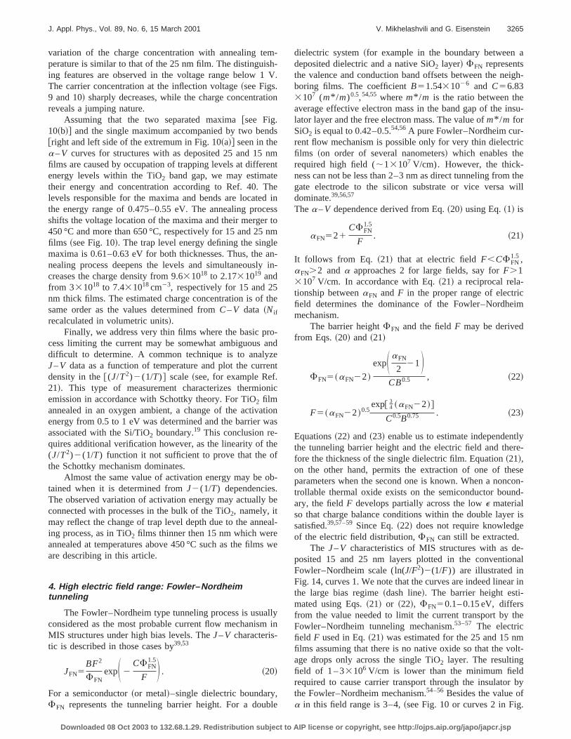
450 °C. This denotes a limitation of the carrier injection dto charges which accumulate on the traps distributed inTiO2 band gap close to the anode~that is near the Si/TiO2 orTiO2/SiO2 boundary!. In the case of field ionization of thetrapping levels,Qm must be less than 12 and 10@see Eq.~8!in Ref. 7# for 15 and 25 nm as deposited films, respectiveThis result confirms once more the conclusion made abthat a Poole–Frenkel contribution to the current transporabsent in our experiments.
The dependencies of the carrier concentration atrapped charge density on applied voltage, calculated by E~12! and~13!, using the experimental data of Figs. 9 andare shown in Fig. 13. The results are for 25 and 15 nm thfilms, as deposited and annealed at 700 and 450 °C, restively. These curves exhibit a decrease in carrier concention in the bulk of the 25 nm TiO2 film by almost two ordersof magnitude, accompanied by an increase of the trapcharge density by a factor of 2–3, as the annealing tempture increases. For the 15 nm TiO2 film, the change in freecarrier concentration is by a factor of about 104 while the
FIG. 13. Trapped charge density and free carrier concentration versuplied voltage of 15~a! and 25 nm~b! thick TiO2 films. Curves 1, 2—asdeposited; curves 18, 28—annealed. Curves 1, 18—charge density; curves 228—free carrier concentration.~a! tann560 min; Tann5450 °C; ~b! tann
560 min; Tann5700 °C.
license or copyright, see http://ojps.aip.org/japo/japcr.jsp
mhV
tio
d
nmeneh
de
r tnlea
th
roanzeen.n
tioa
hef
ob.b
eaes
ll
,b
a
igh-
su-
ric
thewill
im
tlyre-
esecon-nd-
r ise
e-nal
r in
the
molt-
byf.
3265J. Appl. Phys., Vol. 89, No. 6, 15 March 2001 V. Mikhelashvili and G. Eisenstein
variation of the charge concentration with annealing teperature is similar to that of the 25 nm film. The distinguising features are observed in the voltage range below 1The carrier concentration at the inflection voltage~see Figs.9 and 10! sharply decreases, while the charge concentrareveals a jumping nature.
Assuming that the two separated maxima@see Fig.10~b!# and the single maximum accompanied by two ben@right and left side of the extremum in Fig. 10~a!# seen in thea –V curves for structures with as deposited 25 and 15films are caused by occupation of trapping levels at differenergy levels within the TiO2 band gap, we may estimattheir energy and concentration according to Ref. 40. Tlevels responsible for the maxima and bends are locatethe energy range of 0.475–0.55 eV. The annealing procshifts the voltage location of the maxima and their merge450 °C and more than 650 °C, respectively for 15 and 25films ~see Fig. 10!. The trap level energy defining the singmaxima is 0.61–0.63 eV for both thicknesses. Thus, thenealing process deepens the levels and simultaneouslycreases the charge density from 9.631018 to 2.1731019 andfrom 331018 to 7.431018cm23, respectively for 15 and 25nm thick films. The estimated charge concentration is ofsame order as the values determined fromC–V data ~Nif
recalculated in volumetric units!.Finally, we address very thin films where the basic p
cess limiting the current may be somewhat ambiguousdifficult to determine. A common technique is to analyJ–V data as a function of temperature and plot the currdensity in the@(J/T2)2(1/T)# scale~see, for example Ref21!. This type of measurement characterizes thermioemission in accordance with Schottky theory. For TiO2 filmannealed in an oxygen ambient, a change of the activaenergy from 0.5 to 1 eV was determined and the barrier wassociated with the Si/TiO2 boundary.19 This conclusion re-quires additional verification however, as the linearity of t(J/T2)2(1/T) function it not sufficient to prove that the othe Schottky mechanism dominates.
Almost the same value of activation energy may betained when it is determined fromJ2(1/T) dependenciesThe observed variation of activation energy may actuallyconnected with processes in the bulk of the TiO2, namely, itmay reflect the change of trap level depth due to the anning process, as in TiO2 films thinner then 15 nm which werannealed at temperatures above 450 °C such as the filmare describing in this article.
4. High electric field range: Fowler –Nordheimtunneling
The Fowler–Nordheim type tunneling process is usuaconsidered as the most probable current flow mechanismMIS structures under high bias levels. TheJ–V characteris-tic is described in those cases by39,53
JFN5BF2
FFNexpS 2
CFFN1.5
F D . ~20!
For a semiconductor~or metal!–single dielectric boundaryFFN represents the tunneling barrier height. For a dou
Downloaded 08 Oct 2003 to 132.68.1.29. Redistribution subject to AIP
--
.
n
s
t
einssom
n-in-
e
-d
t
ic
ns
-
e
l-
we
yin
le
dielectric system~for example in the boundary betweendeposited dielectric and a native SiO2 layer! FFN representsthe valence and conduction band offsets between the neboring films. The coefficientB51.5431026 and C56.833107 (m* /m)0.5,54,55 wherem* /m is the ratio between theaverage effective electron mass in the band gap of the inlator layer and the free electron mass. The value ofm* /m forSiO2 is equal to 0.42–0.5.54,56A pure Fowler–Nordheim cur-rent flow mechanism is possible only for very thin dielectfilms ~on order of several nanometers! which enables therequired high field (;13107 V/cm). However, the thick-ness can not be less than 2–3 nm as direct tunneling fromgate electrode to the silicon substrate or vice versadominate.39,56,57
Thea –V dependence derived from Eq.~20! using Eq.~1! is
aFN521CFFN
1.5
F. ~21!
It follows from Eq. ~21! that at electric fieldF,CFFN1.5,
aFN.2 and a approaches 2 for large fields, say forF.13107 V/cm. In accordance with Eq.~21! a reciprocal rela-tionship betweenaFN and F in the proper range of electricfield determines the dominance of the Fowler–Nordhemechanism.
The barrier heightFFN and the fieldF may be derivedfrom Eqs.~20! and ~21!
FFN5~aFN22!
expS aFN
221D
CB0.5 , ~22!
F5~aFN22!0.5exp@ 3
4 ~aFN22!#
C0.5B0.75 . ~23!
Equations~22! and~23! enable us to estimate independenthe tunneling barrier height and the electric field and thefore the thickness of the single dielectric film. Equation~21!,on the other hand, permits the extraction of one of thparameters when the second one is known. When a nontrollable thermal oxide exists on the semiconductor bouary, the fieldF develops partially across the lowe materialso that charge balance conditions within the double layesatisfied.39,57–59Since Eq.~22! does not require knowledgof the electric field distribution,FFN can still be extracted.
The J–V characteristics of MIS structures with as dposited 15 and 25 nm layers plotted in the conventioFowler–Nordheim scale (ln(J/F2)2(1/F)) are illustrated inFig. 14, curves 1. We note that the curves are indeed lineathe large bias regime~dash line!. The barrier height esti-mated using Eqs.~21! or ~22!, FFN50.1– 0.15 eV, differsfrom the value needed to limit the current transport byFowler–Nordheim tunneling mechanism.53–57 The electricfield F used in Eq.~21! was estimated for the 25 and 15 nfilms assuming that there is no native oxide so that the vage drops only across the single TiO2 layer. The resultingfield of 1 – 33106 V/cm is lower than the minimum fieldrequired to cause carrier transport through the insulatorthe Fowler–Nordheim mechanism.54–56Besides the value oa in this field range is 3–4,~see Fig. 10 or curves 2 in Fig
license or copyright, see http://ojps.aip.org/japo/japcr.jsp

ll
tarn
o
se
x-
the
iOote
di-he
talmu-
atker,
In
re
3266 J. Appl. Phys., Vol. 89, No. 6, 15 March 2001 V. Mikhelashvili and G. Eisenstein
14! while according to Eq.~21! it must be larger. Hence, aas deposited and annealed TiO2 films, expect for those thin-ner than 15 nm and annealed above 450 °C, do not satisfyconditions for Fowler–Nordheim-type characteristic and criers transport across them has the character of direct tuning.
In order to explain theJ–V curves of annealed 15 nmfilms we assume, as in Ref. 21 that the Si substrate is cered with a thin interfacial SiO2 film. The data in Fig 8~a!curve 3, where a reduction ine with annealing temperature iobserved~for a 15 nm TiO2 film! serves as evidence for thformation of the interfacial SiO2 layer. Considering a simpleseries capacitance model of a double layer TiO2/SiO2 ca-pacitor the SiO2 thickness may be estimated from the etracted accumulation capacitance
LSiO25LTiO2S 12
e
eTiO2
e
eSiO2
21D , ~24!
FIG. 14. The Fowler–Nordheim plots of experimentalJ–V anda –V char-acteristics of as deposited 15~a! and 25 nm~b! thick TiO2 films. Curve 1—J–V; curve 2—a –V. The dash line denotes the linearity ofJ–V curve inFowler–Nordheim scale.
Downloaded 08 Oct 2003 to 132.68.1.29. Redistribution subject to AIP
he-el-
v-
where LSiO2, LTiO2
and eSiO2, eTiO2
are, respectively, thethickness and relative dielectric constant of the SiO2 andTiO2 films. The annealing temperature dependence ofSiO2 thickness, calculated by Eq.~24!, is illustrated in Fig.15 curve 1. Here the relative dielectric constants of the T2
and SiO2 were assumed to be 30 and 3.85, respectively. Nthe significant increase of the SiO2 thickness at 450 °C.
The electric field distribution across a double layerelectric under the condition of charge balance within tdouble dielectric stack is described by39
eF5eSiO2FSiO2
1Q
e05eTiO2
FTiO2. ~25!
Assuming, now, that carriers injected from the gate mepass through the double layer with no charge being acculated at the TiO2 /SiO2 interface (Q/e0,eF), we derivefrom Eqs. ~24! and ~25! the electric field in the SiO2 andTiO2 films
FSiO25
V
eSiO2
eTiO2
LTiO21LSiO2
, ~26!
FTiO25
V
eTiO2
eSiO2
LSiO21LTiO2
, ~27!
whereQ is the charge density ande0 is the permittivity ofvacuum. According to Eqs.~26! and ~27!, the electric fieldacross the ultrathin interfacial layer is quite high, evenmoderate voltages, while the electric field across the thichighere TiO2 layer is low.
The electric field in the SiO2 film is sufficiently high tosatisfy the conditions for Fowler–Nordheim tunneling.Fig. 16 ~curves 1 and 2! we showJ–V anda –V character-istics of a 2.3 nm SiO2 film plotted in the Fowler–Nordheimscale. The curves in Fig. 16 were calculated by Eqs.~25! or~26! usingJ–V date of an MIS structure with a 15 nm TiO2
FIG. 15. The Fowler–Nordheim tunneling barrier height@Eq. ~22!# andcalculated SiO2 thickness@Eq. ~24!# dependencies on annealing temperatuof 15 nm thick TiO2 film. Curve 1—LSiO2
; curve 2—F. tann560 min.
license or copyright, see http://ojps.aip.org/japo/japcr.jsp

tiv
ith
oet
,
.er
-
b
e
lin
cyo
e
d
andThelingthe
thethe
theenm-avet toare
3267J. Appl. Phys., Vol. 89, No. 6, 15 March 2001 V. Mikhelashvili and G. Eisenstein
film, annealed at 700 °C and assuming an effective reladielectric constant of 17@see curve 3 in Fig. 8~a!#. The bar-rier height for this case is 0.89 eV, calculated by Eqs.~21!@or ~22!# and~26! and the data of Fig. 16~curve 2!, whereais linear. The variation of the obtained barrier height wannealing temperature is shown in Fig. 15~curve 2! withsignificant changes seen abobe 500 °C. However, thetained values ofFFN are lower than the actual band offsbetween TiO2 and SiO2 ~which is approximately 2.4 eV!.21
In addition, the quantity ofa at an electric field of;13107 V/cm must be;18 for anFFN on the order of 2.4 eV.
Experimental values ofa in the high voltage rangewhere the calculateda –V dependence~curve 28 in Fig. 16!fits experimental data~curve 2 in Fig. 16!, do not exceed 7Experimental evidence of the sharp change of the FowlNordheim tunneling current in a 4–4.5 nm SiO2 based MISstructure together with an estimateda above 20–25 at electric field of ;13107 V/cm is described in Refs. 54–56~seeFig. 4 in Ref. 54 and Fig. 1 in Ref. 56!.
The low effective barrier heights obtained here maydue to the existence of a current mechanism in additionFowler–Nordheim tunneling, causing a lowering of the thoretical band offset between TiO2 and thermal oxide at highelectric fields. Such a mechanism may be the direct tunnebetween Si and the traps at the SiO2 /TiO2 interface or in theTiO2 bulk as considered for similar double insulator strutures in Refs. 1, 39, 57, and 59. A second explanation mathe internal electric field which develops on the interfacethe TiO2 /SiO2 due to a double charge layer~the observedinflection on theJ–V characteristics or the minimum on tha –V curves of the annealed films, see Figs. 9 and 10!, aidingthe penetration of carriers into the interfacial layer.
5. Leakage current dependence on annealingconditions
Leakage current densities at an electric fieldF5106 V/cm versus annealing temperature and time, are
FIG. 16. The Fowler–Nordheim plots of measured and calculatedJ–V anda –V characteristics of annealed 15 nm thick TiO2 film. Parameters of cal-culation are:FFN50.89 eV andm* /m50.5. The value of the electric fieldfor LSiO2
52.3 nm was calculated in accordance with Eq.~26!. Curves 1,2—measured; curves 18, 28—calculated.tann560 min; Tann5700 °C.
Downloaded 08 Oct 2003 to 132.68.1.29. Redistribution subject to AIP
e
b-
–
eto-
g
-bef
e-
scribed in Fig. 17. For both 15 and 25 nm TiO2 films weobserve an initial sharp reduction of the leakage currenta saturation in the temperature range of 400–500 °C.most drastic change occurs after 10–20 min at anneatemperatures above 700 °C. The total leakage current for25 nm film is reduced from 1 to;1022 A/cm2 while in the15 nm structure, it is reduced from 1 to 531026 A/cm2. Thesharp change in the leakage current density occurs inrange of annealing temperature where the variation ofoptical parameters and the morphology of the TiO2 film andthe interface characteristics of the TiO2/Si boundary, ob-tained fromC–V measurement take place.
A phenomenological model is assumed to explainreduction of leakage current with annealing in an oxygambient. The oxygen molecules, broken by the high teperature, produce excited atoms in single states which hone unoccupied electron orbital and therefore are thoughbe strong electron trap levels. The excited oxygen atomsadsorbed on the surface of the TiO2 film and diffuse into it.
FIG. 17. Leakage current density, measured atF513106 V/cm vs anneal-ing temperature~a! and time~b! of TiO2 films. ~a! tann560 min; ~b! Tann
5700 °C.
license or copyright, see http://ojps.aip.org/japo/japcr.jsp
Onaitea
geg
g
urdat
n1iOe
thfercaO
a
nlA
eea
boftioneng
ngtrnoo.5
vi
otrit
sd-
ort
to-
15
.
ci.
hys.
F.
M.
id,
s.
.
.
tt.
L.
lid-
nt.
3268 J. Appl. Phys., Vol. 89, No. 6, 15 March 2001 V. Mikhelashvili and G. Eisenstein
Diffused excited atoms fill the oxygen vacancies in the Ti2
which are sources of free electrons in the conduction baaccept free electrons, and occupy the lattice site. As thenealing temperature rises, the concentration of the excoxygen atoms increases, the number of vacancies decreand the leakage current lowers. The value of the oxydiffusion coefficient estimated from the data of the leakacurrent density dependence on annealing time@see curve ofthe 15 nm film in Fig. 17~b!# is 10215cm2 s21. This valuewas obtained assuming that the time necessary for oxyatoms to transit across the TiO2 film is determined by thecondition of achieving the required lowering in leakage crent. The large reduction of the leakage current is causethe formation of an interfacial silicon dioxide layer thdominates for films thinner than 15 nm.
With thin SiO2 film, some of the injected carriers catunnel through as occurs for all 25 nm samples and fornm films annealed above 450 °C. The increase of the S2
layer thickness leads to a change in the local electric fidistribution within the TiO2 @see Eq.~27!# and reduces theenergy of carriers, while their barrier increases due toannealing~see curve 2 in Fig. 15!. Note that the increase othe roughness value of thick films annealed at high temptures~see Figs. 3 and 4! causes an enhancement of the loelectric field distribution at the metal contact/roughed Ti2
interface ~similar to the data of Al/Ta2O5 samples!.60 Theresult is an additional difference between the achieved leage current of relatively thick and thin TiO2 films.
IV. CONCLUSION
We have shown a correlation between structural traformations in TiO2 films and its optical and electricacharacteristics—interfacial and current flow properties.large change in all the parameters at an annealing rang350–550 °C and 10–20 min has been determined. The lage current decrease in thick films is basically causeddiffusion of excited oxygen atoms which fill vacanciesoxygen that are the source of free electrons in the conducband of the TiO2. The reason for the carrier flow limitatioin thin L,15 nm films is the additional barrier at thTiO2 /Si boundary which is formed due to the growth durianneling of a 2–2.5 nm thick.
ExperimentalJ–V dependencies were analyzed usithe power exponent procedure. We find that at low elecfields the charge flow into as deposited and annealed 25TiO2 have a hopping nature. The average values of the hping distance between localized states and the impurity cductivity were found to be 2.5–3.5, 4–5 nm and 1310211, 1310211V21 cm21, respectively for 15 and 25nm thick as deposited films. Annealing in an oxygen enronment changes R and s0 to 6 nm and 1310216V21 cm21 for the 25 nm thick film. At a moderateelectric field for any as deposited film the current transpseems to be limited by space charges accumulated onlevels which are located at an energy of 0.475–0.55 eV wdensity ;831018cm23. After annealing they becomedeeper, up to 0.61–0.63 eV with concentration on the orof ;231019cm23. At high electric fields, conventional tun
Downloaded 08 Oct 2003 to 132.68.1.29. Redistribution subject to AIP
d,n-dsesne
en
-by
5
ld
e
a-l
k-
s-
ofk-y
n
icmp-n-
-
rtaph
er
neling may be the basic mechanism for carrier transptrough thin interfacial SiO2 layers in all 25 nm films and lowtemperature annealed 15 nm structures. Direct tunnelinggether with Fowler–Nordhein penetration of the SiO2 seemsto be the current limiting mechanism in structures withnm TiO2 annealed above 450 °C.
1A. C. Rastogi and R. N. Sharma, J. Appl. Phys.71, 5041~1992!.2C. H. Ling, J. Bhaskaran, W. K. Choi, and L. K. Ah, J. Appl. Phys.77,6350 ~1995!.
3M. Agarwal, M. R. DeGuire, and A. H. Heuer, Appl. Phys. Lett.71, 891~1997!.
4F.-C. Chui, J.-J. Wang, J. Y. Lee, and S. C. Wu, J. Appl. Phys.81, 6911~1997!.
5W. S. Lau, L. Zrong, Allen Lee, and C. H. See, Appl. Phys. Lett.71, 500~1997!.
6H.-J. Lee, R. Sinclair, M.-B. Lee, and H.-D. Lee, J. Appl. Phys.83, 139~1998!.
7V. Mikhelashvili, Y. Betzer, I. Prudnikov, M. Orenstein, D. Ritter, and GEisenstein, J. Appl. Phys.84, 6747~1998!.
8V. Mikhelashvili and G. Eisenstein, Appl. Phys. Lett.75, 2836~1999!.9C. Chaneliere, J. L. Autran, B. Balland, and R. A. B. Devine, Mater. SEng., R.22, 269 ~1998!.
10H. Tang, K. Prasad, R. Sanjines, P. E. Schmid, and F. Levy, J. Appl. P75, 2042~1994!.
11D. G. Howitt and A. B. Harker, J. Mater. Sci.2, 201 ~1987!.12F. Edelman, A. Rotshild, Y. Komem, V. Mikhelashvili, A. Chack, and
Cosandey, Electron Technology~Institute of Electron Technology,Warszawa, 2000!, Vol. 33, p. 89.
13J. D. Deloach, G. Scarel, and C. R. Aita, J. Appl. Phys.85, 2377~1999!.14P. Alexandrov, J. Koprinarova, and D. Todorov, Solid-State Electron.47,
1333 ~1996!.15M. Mosaddeq-ur-Rahman, G. Yu, T. Soga, T. Jimbo, H. Ebisu, and
Umeno, J. Appl. Phys.88, 4634~2000!.16C. Ting, S. Chen, and D. Liu, J. Appl. Phys.88, 4628~2000!.17T. Fuyiki and H. Matsunami, Jpn. J. Appl. Phys., Part 125, 1288~1986!.18N. Rausch and E. P. Burte, J. Electrochem. Soc.140, 145 ~1993!.19J. Yan, D. C. Gilmer, S. A. Campbell, W. L. Gladfelter, and P. G. Schm
J. Vac. Sci. Technol. B14, 1706~1996!.20H.-S. Kim, D. C. Gilmer, S. A. Campbell, and D. L. Polla, Appl. Phy
Lett. 69, 3860~1996!.21S. A. Campbell, H. S. Kim, D. C. Gilmer, B. He, T. Ma, and W. L
Gladfelter~unpublished!.22S. A. Campbell, D. C. Gilmer, X.-C. Wang, M.-T. Hsieh, H.-S. Kim, W
L. Gladfelter, and J. Yan, IEEE Trans. Electron Devices44, 104 ~1997!.23H.-S. Kim, S. A. Campbell, and D. C. Gilmer, IEEE Electron Device Le
18, 465 ~1997!.24H.-S. Kim, S. A. Campbell, D. C. Gilmer, V. Kaushik, J. Conner,
Prabhu, and A. Anderson, J. Appl. Phys.85, 3278~1999!.25R. F. Cava, W. F. Peck, Jr., and J. J. Krajewski, Nature~London! 377, 215
~1995!.26J.-Y. Gan, Y. C. Chang, and T. B. Wu, Appl. Phys. Lett.72, 332 ~1998!.27A. Cappellani, J. L. Keddie, N. P. Barradas, and S. M. Jeckson, So
State Electron.43, 1095~1999!.28W. D. Brown and W. W. Grannemann, Solid-State Electron.21, 837
~1978!.29V. Mikhelashvili and G. Eisenstein, Microelectron. Reliab.40, 657
~2000!.30V. Mikhelashvili and G. Eisenstein, IEEE Trans. Electron Devices~to be
published!.31H. Tang, F. Levy, H. Berger, and P. E. Schmid, Phys. Rev. B52, 7771
~1995!.32H. Tang, H. Berger, P. E. Schmid, and F. Levy, Solid State Commun.87,
847 ~1993!.33A. C. Adams, inVLSI Technology, edited by S. M. Sze~McGraw-Hill,
New York, 1983!.34L. S. Hsu, R. Rujkorakarn, J. R. Sites, and C. Y. She, J. Appl. Phys.59,
3475 ~1986!.35The Encyclopedia of Advanced Materials, Vol. 4, edited by R. W. Cahn
~Elsevier, New York, 1994!, p. 2880.36Y. Jeon, B. H. Lee, K. Zavadzki, W. Qi, and J. C. Lee, Tech. Dig. I
Electron Devices Meet. 797~1998!.
license or copyright, see http://ojps.aip.org/japo/japcr.jsp
ke
-o,
it-
-
ors
.
J.
J.
c.
3269J. Appl. Phys., Vol. 89, No. 6, 15 March 2001 V. Mikhelashvili and G. Eisenstein
37G. B. Alers, D. J. Werder, Y. Chabal, H. C. Lu, E. P. Gusev, E. GarfunT. Gustafsson, and R. S. Urdal, Appl. Phys. Lett.73, 1517~1998!.
38B. H. Lee, Y. Jeon, K. Zavadzki, W. Qi, and J. Lee, Appl. Phys. Lett.74,3143 ~1999!.
39S. M. Sze, inPhysics of Semiconductor Devices~Wiley Interscience, NewYork, 1969!.
40A. N. Zyuganov and S. V. Svechnikov,Injection Contact Phenomena inSemiconductors~Naukova Dumka, Kiev, 1981!, in Russian.
41A. N. Zyuganov, V. V. Zorikov, M. S. Matinova, V. M. Mikhelashvili,and R. I. Chikovani, Sov. Tech. Phys. Lett.7, 493 ~1981!.
42G. D. Bagratishvili, R. B. Dzanelidze, D. A. Jishiashvili, L. V. Piskanovski, A. N. Zyuganov, V. M. Mikhelashvili, and P. S. SmertenkPhys. Status Solidi A65, 701 ~1981!.
43V. Mikhelashvili, G. Eisenstein, V. Garber, S. Fainleib, G. Bahir, D. Rter, M. Orenstein, and A. Peer, J. Appl. Phys.85, 6873~1999!.
44V. Mikhelashvili and G. Eisenstein, J. Appl. Phys.86, 6965~1999!.45V. Mikhelashvili, G. Eisenstein, and R. Uzdin, Solid-State Electron.45,
143 ~2001!.46N. F. Mott and E. A. Davis,Electron Processes in Non-Crystalline Mate
rials ~Clarendon, Oxford, 1979!.47in Electronic and Structural Properties of Amorphous Semiconduct,
Downloaded 08 Oct 2003 to 132.68.1.29. Redistribution subject to AIP
l, edited by P. G. LeComber and J. Mort~Academic, New York, 1972!.48V. N. Bogomolov, E. K. Kudinov, D. N. Mirlin, and Yu. A. Firsov, Sov
Phys. Solid State19, 1630~1968!.49J. C. Pfister, Phys. Status Solidi A24, k15 ~1974!.50A. Rose, Phys. Rev.97, 1538~1955!.51M. A. Lampert, RCA Rev.20, 682 ~1959!.52M. A. Lampert and P. Mark,Current Injection in Solids~Academic, New
York, 1970!.53J. G. Simmons, J. Appl. Phys.34, 1793~1963!.54S. Zafar, Q. Liu, and E. A. Irene, J. Vac. Sci. Technol. A13, 47 ~1995!.55S. Zafar, K. A. Konrad, Q. Liu, E. A. Irene, G. Hames, R. Kuehn, and
J. Wortmann, Appl. Phys. Lett.67, 1031~1995!.56M. V. Fischetti, D. J. DiMaria, L. Dori, J. Batey, E. Tierney, and
Stasiak, Phys. Rev. B , 4404~1987!.57in Silicon Integrated Circuits, Part A, edited by D. Cahng~Academic,
New York, 1981!.58G. W. Taylor and J. G. Simmons, Solid-State Electron.17, 1 ~1974!.59Y. Nishioka, S. Kimura, H. Shinriki, and K. Mukai, J. Electrochem. So
13, 410 ~1987!.60Y. S. Kim, Y. H. Lee, K. M. Lim, and M. Y. Sung, Appl. Phys. Lett.74,
2800 ~1999!.
license or copyright, see http://ojps.aip.org/japo/japcr.jsp