efficient embedded computing a …cva.stanford.edu/publications/2010/jbalfour-thesis.pdfefficient...
TRANSCRIPT

EFFICIENT EMBEDDED COMPUTING
A DISSERTATIONSUBMITTED TO THE DEPARTMENT OF ELECTRICAL ENGINEERING
AND THE COMMITTEE ON GRADUATE STUDIESOF STANFORD UNIVERSITY
IN PARTIAL FULFILLMENT OF THE REQUIREMENTSFOR THE DEGREE OF
DOCTOR OF PHILOSOPHY
James David BalfourMay 2010

http://creativecommons.org/licenses/by-nc/3.0/us/
This dissertation is online at: http://purl.stanford.edu/nb912df4852
© 2010 by James David Balfour. All Rights Reserved.
Re-distributed by Stanford University under license with the author.
This work is licensed under a Creative Commons Attribution-Noncommercial 3.0 United States License.
ii

I certify that I have read this dissertation and that, in my opinion, it is fully adequatein scope and quality as a dissertation for the degree of Doctor of Philosophy.
William Dally, Primary Adviser
I certify that I have read this dissertation and that, in my opinion, it is fully adequatein scope and quality as a dissertation for the degree of Doctor of Philosophy.
Mark Horowitz
I certify that I have read this dissertation and that, in my opinion, it is fully adequatein scope and quality as a dissertation for the degree of Doctor of Philosophy.
Christoforos Kozyrakis
Approved for the Stanford University Committee on Graduate Studies.
Patricia J. Gumport, Vice Provost Graduate Education
This signature page was generated electronically upon submission of this dissertation in electronic format. An original signed hard copy of the signature page is on file inUniversity Archives.
iii
Abstract
Embedded computer systems are ubiquitous, and contemporary embedded applications exhibit demandingcomputation and efficiency requirements. Meeting these demands presently requires the use of application-specific integrated circuits and collections of complex system-on-chip components. The design and imple-mentation of application-specific integrated circuits is both expensive and time consuming. Most of theeffort and expense arises from the non-recurring engineering activities required to manually lower high-leveldescriptions of systems to equivalent low-level descriptions that are better suited to hardware realization.Programmable systems, particularly those that can be targeted effectively using high-level programming lan-guages, offer reduced development costs and faster design times. They also offer the flexibility requiredto upgrade previously deployed systems as new standards and applications are developed. However, pro-grammable systems are less efficient than fixed-function hardware. This significantly limits the class ofapplications for which programamble processors are an acceptable alternatives to application-specific fixed-function hardware, as efficiency demands often preclude the use of programmable hardware. With mostcontemporary computer systems limited by efficiency, improving the efficiency of programmable systems isa critical challenge and an active area of computer systems research.
This dissertation describes Elm, an efficient programmable system for high-performance embedded ap-plications. Elm is significantly more efficient than conventional embedded processors on compute-intensivekernels. Elm allows software to exploit parallelism to achieve performance while managing locality to achieveefficiency. Elm implements a novel distributed and hierarchical system organization that allows software toexploit the abundant parallelism, reuse, and locality that are present in embedded applications. Elm provides avariety of mechanisms to assist software in mapping applications efficiently to massively parallel systems. Toimprove efficiency, Elm allows software to explicitly schedule and orchestrate the movement and placementof instructions and data.
This dissertation proposes and critically analyzes concepts that encompass the interaction of computer ar-chitecture, compiler technology, and VLSI circuits to increase performance and efficiency in modern embed-ded computer systems. A central theme of this dissertation is that the efficiency of programmable embeddedsystems can be improved significantly by exposing deep and distributed storage hierarchies to software. Thisallows software to exploit temporal and spatial reuse and locality at multiple levels in applications in order toreduce instruction and data movement.
iv
Acknowledgments
First, I would like to thank my dissertation advisor, Professor William J. Dally, who has been great mentorand teacher. I benefited immensely from Bill’s technical insight, vast experience, boundless enthusiasm, andsteadfast support.
I would like to thank the other members of my dissertation committee, Professors Mark Horowitz, Chris-tos Kozyrakis, and Boris Murmann. I had the distinct pleasure of having all three as lecturers at varioustimes while a graduate student, and benefited greatly from their insights and experience. I imagine all willrecognize some aspects of their teaching and influence within this dissertation.
I was fortunate to befriend some fantastic folks while at Stanford. In particular, I would like to thankMichael Linderman for years of engaging early morning discussions, and Catie Chang for years of engaginglate night discussions and encouragement; my first few years at Stanford would not have been nearly as tol-erable without their friendship. I would like the thank James Kierstead for several years of Sunday morningsspent discussing the plight of graduate students over waffles and coffee.
I particularly want to thank Tanya for her friendship, patience, support, assistance, and understanding.The last year would have been difficult without her.
I should like to acknowledge the other members of the concurrent VLSI architecture group at Stanfordthat I had the benefit of interacting with. In particular, I would like to acknowledge the efforts of the othermembers of the efficient embedded computing group. In approximate chronological order: David Black-Schaffer, Jongsoo Park, Vishal Parikh, R. Curtis Harting, and David Sheffield. I also had the pleasure ofsharing an office with Ted Jiang, which I appreciated. Ted was always around and cheery on weekends,which made Sundays in the office more enjoyable, and kept the bookshelves well stocked.
While a student at Stanford, I was funded in part by a Stanford Graduate Fellowship that was endowedby Cadence Design Systems. I remain grateful for the support.
Finally, I would like to thank my family for all the love and support they have provided through the years.
v

Dedicated to the memory of Harold T. Fargey,who passed away before I could share my writingwith him as he always shared with me.
vi
Contents
Abstract iv
Acknowledgments v
1 Introduction 11.1 Embedded Computing . . . . . . . . . . . . . . . . . . . . . . . . . . . . . . . . . . . . . 2
1.2 Technology and System Trends . . . . . . . . . . . . . . . . . . . . . . . . . . . . . . . . . 4
1.3 A Simple Problem of Productivity and Efficiency . . . . . . . . . . . . . . . . . . . . . . . 5
1.4 Collaboration and Previous Publications . . . . . . . . . . . . . . . . . . . . . . . . . . . . 6
1.5 Dissertation Contributions . . . . . . . . . . . . . . . . . . . . . . . . . . . . . . . . . . . 6
1.6 Dissertation Organization . . . . . . . . . . . . . . . . . . . . . . . . . . . . . . . . . . . . 8
2 Contemporary Embedded Architectures 102.1 The Efficiency Impediments of Programmable Systems . . . . . . . . . . . . . . . . . . . . 10
2.2 Common Strategies for Improving Efficiency . . . . . . . . . . . . . . . . . . . . . . . . . 16
2.3 A Survey of Related Contemporary Architectures . . . . . . . . . . . . . . . . . . . . . . . 20
2.4 Chapter Summary . . . . . . . . . . . . . . . . . . . . . . . . . . . . . . . . . . . . . . . . 23
3 The Elm Architecture 243.1 Concepts . . . . . . . . . . . . . . . . . . . . . . . . . . . . . . . . . . . . . . . . . . . . 24
3.2 System Architecture . . . . . . . . . . . . . . . . . . . . . . . . . . . . . . . . . . . . . . . 25
3.3 Programming and Compilation . . . . . . . . . . . . . . . . . . . . . . . . . . . . . . . . . 32
3.4 Chapter Summary . . . . . . . . . . . . . . . . . . . . . . . . . . . . . . . . . . . . . . . . 36
4 Instruction Registers 374.1 Concepts . . . . . . . . . . . . . . . . . . . . . . . . . . . . . . . . . . . . . . . . . . . . 37
4.2 Microarchitecture . . . . . . . . . . . . . . . . . . . . . . . . . . . . . . . . . . . . . . . . 44
4.3 Examples . . . . . . . . . . . . . . . . . . . . . . . . . . . . . . . . . . . . . . . . . . . . 47
4.4 Allocation and Scheduling . . . . . . . . . . . . . . . . . . . . . . . . . . . . . . . . . . . 59
4.5 Evaluation and Analysis . . . . . . . . . . . . . . . . . . . . . . . . . . . . . . . . . . . . 67
4.6 Related Work . . . . . . . . . . . . . . . . . . . . . . . . . . . . . . . . . . . . . . . . . . 78
vii

4.7 Chapter Summary . . . . . . . . . . . . . . . . . . . . . . . . . . . . . . . . . . . . . . . . 80
5 Operand Registers and Explicit Operand Forwarding 815.1 Concepts . . . . . . . . . . . . . . . . . . . . . . . . . . . . . . . . . . . . . . . . . . . . 81
5.2 Microarchitecture . . . . . . . . . . . . . . . . . . . . . . . . . . . . . . . . . . . . . . . . 85
5.3 Example . . . . . . . . . . . . . . . . . . . . . . . . . . . . . . . . . . . . . . . . . . . . . 87
5.4 Allocation and Scheduling . . . . . . . . . . . . . . . . . . . . . . . . . . . . . . . . . . . 89
5.5 Evaluation . . . . . . . . . . . . . . . . . . . . . . . . . . . . . . . . . . . . . . . . . . . . 94
5.6 Related Work . . . . . . . . . . . . . . . . . . . . . . . . . . . . . . . . . . . . . . . . . . 102
5.7 Chapter Summary . . . . . . . . . . . . . . . . . . . . . . . . . . . . . . . . . . . . . . . . 102
6 Indexed and Address-Stream Registers 1046.1 Concepts . . . . . . . . . . . . . . . . . . . . . . . . . . . . . . . . . . . . . . . . . . . . 104
6.2 Microarchitecture . . . . . . . . . . . . . . . . . . . . . . . . . . . . . . . . . . . . . . . . 106
6.3 Examples . . . . . . . . . . . . . . . . . . . . . . . . . . . . . . . . . . . . . . . . . . . . 113
6.4 Evaluation and Analysis . . . . . . . . . . . . . . . . . . . . . . . . . . . . . . . . . . . . 122
6.5 Related Work . . . . . . . . . . . . . . . . . . . . . . . . . . . . . . . . . . . . . . . . . . 128
6.6 Chapter Summary . . . . . . . . . . . . . . . . . . . . . . . . . . . . . . . . . . . . . . . . 131
7 Ensembles of Processors 1327.1 Concept . . . . . . . . . . . . . . . . . . . . . . . . . . . . . . . . . . . . . . . . . . . . . 132
7.2 Microarchitecture . . . . . . . . . . . . . . . . . . . . . . . . . . . . . . . . . . . . . . . . 137
7.3 Examples . . . . . . . . . . . . . . . . . . . . . . . . . . . . . . . . . . . . . . . . . . . . 139
7.4 Allocation and Scheduling . . . . . . . . . . . . . . . . . . . . . . . . . . . . . . . . . . . 143
7.5 Evaluation and Analysis . . . . . . . . . . . . . . . . . . . . . . . . . . . . . . . . . . . . 146
7.6 Related Work . . . . . . . . . . . . . . . . . . . . . . . . . . . . . . . . . . . . . . . . . . 149
7.7 Chapter Summary . . . . . . . . . . . . . . . . . . . . . . . . . . . . . . . . . . . . . . . . 152
8 The Elm Memory System 1538.1 Concepts . . . . . . . . . . . . . . . . . . . . . . . . . . . . . . . . . . . . . . . . . . . . 153
8.2 Microarchitecture . . . . . . . . . . . . . . . . . . . . . . . . . . . . . . . . . . . . . . . . 165
8.3 Example . . . . . . . . . . . . . . . . . . . . . . . . . . . . . . . . . . . . . . . . . . . . . 177
8.4 Evaluation and Analysis . . . . . . . . . . . . . . . . . . . . . . . . . . . . . . . . . . . . 179
8.5 Related Work . . . . . . . . . . . . . . . . . . . . . . . . . . . . . . . . . . . . . . . . . . 189
8.6 Chapter Summary . . . . . . . . . . . . . . . . . . . . . . . . . . . . . . . . . . . . . . . . 191
9 Conclusion 1929.1 Summary of Thesis and Contributions . . . . . . . . . . . . . . . . . . . . . . . . . . . . . 192
9.2 Future Work . . . . . . . . . . . . . . . . . . . . . . . . . . . . . . . . . . . . . . . . . . . 193
viii

A Experimental Methodology 196A.1 Performance Modeling and Estimation . . . . . . . . . . . . . . . . . . . . . . . . . . . . . 196A.2 Power and Energy Modeling . . . . . . . . . . . . . . . . . . . . . . . . . . . . . . . . . . 197
B Descriptions of Kernels and Benchmarks 200B.1 Description of Kernels . . . . . . . . . . . . . . . . . . . . . . . . . . . . . . . . . . . . . 200B.2 Benchmarks . . . . . . . . . . . . . . . . . . . . . . . . . . . . . . . . . . . . . . . . . . . 204
C Elm Instruction Set Architecture Reference 206C.1 Control Flow and Instruction Registers . . . . . . . . . . . . . . . . . . . . . . . . . . . . . 206C.2 Operand Registers and Explicit Operand Forwarding . . . . . . . . . . . . . . . . . . . . . 210C.3 Indexed Registers and Address-Stream Registers . . . . . . . . . . . . . . . . . . . . . . . 213C.4 Ensembles and Processor Corps . . . . . . . . . . . . . . . . . . . . . . . . . . . . . . . . 217C.5 Memory System . . . . . . . . . . . . . . . . . . . . . . . . . . . . . . . . . . . . . . . . . 222
Bibliography 234
ix
List of Tables
1.1 Estimates of Energy Expended Performing Common Operations . . . . . . . . . . . . . . . 7
2.1 Embedded RISC Processor Information . . . . . . . . . . . . . . . . . . . . . . . . . . . . 112.2 Average Energy Per Instruction for an Embedded RISC Processor . . . . . . . . . . . . . . 17
4.1 Elm Instruction Fetch Energy . . . . . . . . . . . . . . . . . . . . . . . . . . . . . . . . . . 76
5.1 Energy Consumed by Common Operations . . . . . . . . . . . . . . . . . . . . . . . . . . 87
8.1 Execution Times and Data Transferred . . . . . . . . . . . . . . . . . . . . . . . . . . . . . 1798.2 Number of Remote and Stream Memory Operations in Benchmarks . . . . . . . . . . . . . 187
C.1 Mapping of Message Registers to Communication Links . . . . . . . . . . . . . . . . . . . 218
x
List of Figures
2.1 Embedded RISC Processor Area . . . . . . . . . . . . . . . . . . . . . . . . . . . . . . . . 12
2.2 Average Instructions Per Cycle for an Embedded RISC Processor . . . . . . . . . . . . . . . 12
2.3 Energy Consumption by Module for an Embedded RISC Processor . . . . . . . . . . . . . . 13
2.4 Distribution of Instructions by Operation Type in Embedded Kernels . . . . . . . . . . . . . 14
2.5 Distribution of Instructions within Embedded Kernels . . . . . . . . . . . . . . . . . . . . . 15
2.6 Distribution of Energy Consumption within Embedded Kernels . . . . . . . . . . . . . . . . 16
3.1 Elm System Architecture . . . . . . . . . . . . . . . . . . . . . . . . . . . . . . . . . . . . 25
3.2 Elm Communication and Storage Hierarchy . . . . . . . . . . . . . . . . . . . . . . . . . . 26
3.3 Elk Actor Concept . . . . . . . . . . . . . . . . . . . . . . . . . . . . . . . . . . . . . . . 33
3.4 Elk Bundle Concept . . . . . . . . . . . . . . . . . . . . . . . . . . . . . . . . . . . . . . . 34
3.5 Elk Stream Concept . . . . . . . . . . . . . . . . . . . . . . . . . . . . . . . . . . . . . . . 34
3.6 Elk Implementation of FFT . . . . . . . . . . . . . . . . . . . . . . . . . . . . . . . . . . . 35
4.1 Instruction Register Organization . . . . . . . . . . . . . . . . . . . . . . . . . . . . . . . . 38
4.2 Impact of Cache Block Size on Miss Rate and Instructions Transferred . . . . . . . . . . . . 43
4.3 Instruction Register Microarchitecture . . . . . . . . . . . . . . . . . . . . . . . . . . . . . 45
4.4 Assembly Code Fragment of a Loop that can be Captured in Instruction Registers . . . . . . 48
4.5 Assembly Code Produced with a Simple Allocation and Scheduling Strategy . . . . . . . . . 49
4.6 Assembly Code Fragment Produced when Instruction Load is Advanced . . . . . . . . . . . 50
4.7 Assembly Code Fragment with a Loop that Exceeds the Instruction Register Capacity . . . . 51
4.8 Loop after Basic Instruction Load Scheduling . . . . . . . . . . . . . . . . . . . . . . . . . 52
4.9 Assembly Code After Partitioning Loop Body Into 3 Basic Blocks . . . . . . . . . . . . . . 53
4.10 Assembly Code After Load Scheduling . . . . . . . . . . . . . . . . . . . . . . . . . . . . 54
4.11 Assembly Code Fragment Illustrating a Procedure Call . . . . . . . . . . . . . . . . . . . . 55
4.12 Assembly Code Fragment Illustrating Function Call Using Function Pointer . . . . . . . . . 56
4.13 Assembly Code Illustrating Indirect Jump . . . . . . . . . . . . . . . . . . . . . . . . . . . 57
4.14 Assembly Fragment Containing a Loop with a Control-Flow Statement . . . . . . . . . . . 58
4.15 Contents of Instruction Registers During Loop Execution . . . . . . . . . . . . . . . . . . . 59
4.16 Control-Flow Graph . . . . . . . . . . . . . . . . . . . . . . . . . . . . . . . . . . . . . . . 60
xi

4.17 Illustration of Regions in the Control-Flow Graph . . . . . . . . . . . . . . . . . . . . . . . 624.18 Resident Instruction Sets . . . . . . . . . . . . . . . . . . . . . . . . . . . . . . . . . . . . 644.19 Kernel Code Size After Instruction Register Allocation and Scheduling . . . . . . . . . . . 674.20 Static Fraction of Instruction Pairs that Load Instructions . . . . . . . . . . . . . . . . . . . 684.21 Normalized Kernel Execution Time . . . . . . . . . . . . . . . . . . . . . . . . . . . . . . 694.22 Fraction of Issued Instruction Pairs that Contain Instruction Loads . . . . . . . . . . . . . . 704.23 Normalized Instruction Bandwidth Demand . . . . . . . . . . . . . . . . . . . . . . . . . . 714.24 Direct-Mapped Filter Cache Bandwidth Demand . . . . . . . . . . . . . . . . . . . . . . . 734.25 Fully-Associative Filter Cache Bandwidth Demand . . . . . . . . . . . . . . . . . . . . . . 744.26 Comparison of Instructions Loaded Using Filter Caches and Instruction Registers . . . . . . 754.27 Instruction Delivery Energy . . . . . . . . . . . . . . . . . . . . . . . . . . . . . . . . . . . 77
5.1 Operand Register Organization . . . . . . . . . . . . . . . . . . . . . . . . . . . . . . . . . 845.2 Operand Register Microarchitecture . . . . . . . . . . . . . . . . . . . . . . . . . . . . . . 865.3 Intermediate Representation . . . . . . . . . . . . . . . . . . . . . . . . . . . . . . . . . . 885.4 Assembly for Conventional Register Organization . . . . . . . . . . . . . . . . . . . . . . . 885.5 Assembly Using Explicit Forwarding and Operand Registers . . . . . . . . . . . . . . . . . 895.6 Calculation of Operand Appearances . . . . . . . . . . . . . . . . . . . . . . . . . . . . . . 925.7 Calculation of Operand Intensity . . . . . . . . . . . . . . . . . . . . . . . . . . . . . . . . 935.8 Impact of Operand Registers on Data Bandwidth . . . . . . . . . . . . . . . . . . . . . . . 955.9 Operand and Result Bandwidth . . . . . . . . . . . . . . . . . . . . . . . . . . . . . . . . . 965.10 Impact of Register Organization on Data Energy . . . . . . . . . . . . . . . . . . . . . . . . 985.11 Execution Time . . . . . . . . . . . . . . . . . . . . . . . . . . . . . . . . . . . . . . . . . 100
6.1 Index Registers and Address-stream Registers . . . . . . . . . . . . . . . . . . . . . . . . . 1076.2 Finite Impulse Response Filter Kernel . . . . . . . . . . . . . . . . . . . . . . . . . . . . . 1146.3 Finite Impulse Response Filter . . . . . . . . . . . . . . . . . . . . . . . . . . . . . . . . . 1146.4 Assembly Fragment Showing Scheduled Inner Loop of FIR Kernel . . . . . . . . . . . . . . 1156.5 Assembly Fragment Showing use of Index Registers in Inner Loop of fir Kernel . . . . . . . 1166.6 Assembly Fragment Showing use of Address-stream Registers in Inner Loop of fir Kernel . . 1166.7 Illustration of Image Convolution . . . . . . . . . . . . . . . . . . . . . . . . . . . . . . . . 1176.8 Image Convolution Kernel . . . . . . . . . . . . . . . . . . . . . . . . . . . . . . . . . . . 1176.9 Assembly Fragment for Convolution Kernel . . . . . . . . . . . . . . . . . . . . . . . . . . 1196.10 Assembly Fragment for Convolution Kernel using Address-Stream Registers . . . . . . . . 1196.11 Convolution Kernel using Indexed Registers . . . . . . . . . . . . . . . . . . . . . . . . . . 1206.12 Convolution Kernel using Vector Loads . . . . . . . . . . . . . . . . . . . . . . . . . . . . 1216.13 Data Reuse in Indexed Registers . . . . . . . . . . . . . . . . . . . . . . . . . . . . . . . . 1216.14 Static Kernel Code Size . . . . . . . . . . . . . . . . . . . . . . . . . . . . . . . . . . . . . 1226.15 Dynamic Kernel Instruction Count . . . . . . . . . . . . . . . . . . . . . . . . . . . . . . . 1236.16 Normalized Kernel Execution Times . . . . . . . . . . . . . . . . . . . . . . . . . . . . . . 125
xii
6.17 Normalized Kernel Instruction Energy . . . . . . . . . . . . . . . . . . . . . . . . . . . . . 1266.18 Normalized Kernel Data Energy . . . . . . . . . . . . . . . . . . . . . . . . . . . . . . . . 127
7.1 Ensemble of Processors . . . . . . . . . . . . . . . . . . . . . . . . . . . . . . . . . . . . . 1337.2 Group Instruction Issue Microarchitecture . . . . . . . . . . . . . . . . . . . . . . . . . . . 1387.3 Composing and Receiving Messages in Indexed Registers . . . . . . . . . . . . . . . . . . . 1407.4 Source Code Fragment for Parallelized fir . . . . . . . . . . . . . . . . . . . . . . . . . . . 1417.5 Mapping of fir Data, Computation, and Communication to an Ensemble . . . . . . . . . . . 1427.6 Assembly Listing of Parallel fir Kernel . . . . . . . . . . . . . . . . . . . . . . . . . . . . . 1427.7 Mapping of Instruction Blocks to Instruction Registers . . . . . . . . . . . . . . . . . . . . 1437.8 Parallel fir Kernel Instruction Fetch and Issue Schedule . . . . . . . . . . . . . . . . . . . . 1447.9 Shared Instruction Register Allocation . . . . . . . . . . . . . . . . . . . . . . . . . . . . . 1457.10 Normalized Latency of Parallelized Kernels . . . . . . . . . . . . . . . . . . . . . . . . . . 1467.11 Normalized Throughput of Parallelized Kernels . . . . . . . . . . . . . . . . . . . . . . . . 1477.12 Aggregate Instruction Energy . . . . . . . . . . . . . . . . . . . . . . . . . . . . . . . . . . 1487.13 Normalized Instruction Energy . . . . . . . . . . . . . . . . . . . . . . . . . . . . . . . . . 148
8.1 Elm Memory Hierarchy . . . . . . . . . . . . . . . . . . . . . . . . . . . . . . . . . . . . . 1548.2 Elm Address Space . . . . . . . . . . . . . . . . . . . . . . . . . . . . . . . . . . . . . . . 1568.3 Flexible Cache Hierarchy . . . . . . . . . . . . . . . . . . . . . . . . . . . . . . . . . . . . 1588.4 Stream Load using Non-Unit Stride Addressing . . . . . . . . . . . . . . . . . . . . . . . . 1608.5 Stream Store using Non-Unit Stride Addressing . . . . . . . . . . . . . . . . . . . . . . . . 1608.6 Stream Load using Indexed Addressing . . . . . . . . . . . . . . . . . . . . . . . . . . . . 1618.7 Stream Store using Indexed Addressing . . . . . . . . . . . . . . . . . . . . . . . . . . . . 1618.8 Local Ensemble Memory Interleaving . . . . . . . . . . . . . . . . . . . . . . . . . . . . . 1628.9 Memory Tile Architecture . . . . . . . . . . . . . . . . . . . . . . . . . . . . . . . . . . . 1668.10 Cache Architecture . . . . . . . . . . . . . . . . . . . . . . . . . . . . . . . . . . . . . . . 1688.11 Stream Architecture . . . . . . . . . . . . . . . . . . . . . . . . . . . . . . . . . . . . . . . 1708.12 Formats used by read Messages . . . . . . . . . . . . . . . . . . . . . . . . . . . . . . . . 1718.13 Formats used for write Messages . . . . . . . . . . . . . . . . . . . . . . . . . . . . . . . . 1728.14 Formats used for compare-and-swap Messages . . . . . . . . . . . . . . . . . . . . . . . . 1728.15 Formats used by fetch-and-add Messages . . . . . . . . . . . . . . . . . . . . . . . . . . . 1728.16 Formats of copy Messages . . . . . . . . . . . . . . . . . . . . . . . . . . . . . . . . . . . 1738.17 Formats of read-stream Messages . . . . . . . . . . . . . . . . . . . . . . . . . . . . . . . 1738.18 Formats of write-stream messages . . . . . . . . . . . . . . . . . . . . . . . . . . . . . . . 1748.19 Formats of read-cache messages . . . . . . . . . . . . . . . . . . . . . . . . . . . . . . . . 1748.20 Formats of write-cache messages . . . . . . . . . . . . . . . . . . . . . . . . . . . . . . . 1758.21 Formats of read-stream-cache messages . . . . . . . . . . . . . . . . . . . . . . . . . . . 1758.22 Formats of write-stream-cache messages . . . . . . . . . . . . . . . . . . . . . . . . . . . 1768.23 Format of execute Command Messages . . . . . . . . . . . . . . . . . . . . . . . . . . . . 176
xiii

8.24 Format of dispatch Command Messages . . . . . . . . . . . . . . . . . . . . . . . . . . . 1778.25 Examples of Array-of-Structures and Structure-of-Arrays Data Types . . . . . . . . . . . . 1778.26 Scalar Conversion Between Array-of-Structures and Structure-of-Arrays . . . . . . . . . . . 1788.27 Stream Conversion Between Array-of-Structures and Structures-of-Arrays . . . . . . . . . . 1788.28 Image Filter Kernel . . . . . . . . . . . . . . . . . . . . . . . . . . . . . . . . . . . . . . . 1808.29 Implementation using Remote Loads and Stores [Kernel 1] . . . . . . . . . . . . . . . . . . 1818.30 Implementation using Decoupled Remote Loads and Stores [Kernel 2] . . . . . . . . . . . . 1828.31 Implementation using Block Gets and Puts [Kernel 3] . . . . . . . . . . . . . . . . . . . . . 1828.32 Implementation using Decoupled Block Gets and Puts [Kernel 4] . . . . . . . . . . . . . . . 1838.33 Implementation using Stream Loads and Stores [Kernel 5] . . . . . . . . . . . . . . . . . . 1848.34 Normalized Kernel Execution Times . . . . . . . . . . . . . . . . . . . . . . . . . . . . . . 1858.35 Memory Bandwidth Demand . . . . . . . . . . . . . . . . . . . . . . . . . . . . . . . . . . 1868.36 Normalized Memory Access Breakdown . . . . . . . . . . . . . . . . . . . . . . . . . . . . 1868.37 Normalized Memory Messages . . . . . . . . . . . . . . . . . . . . . . . . . . . . . . . . . 1878.38 Normalized Memory Message Data . . . . . . . . . . . . . . . . . . . . . . . . . . . . . . 188
C.1 Encoding of Jump Instructions . . . . . . . . . . . . . . . . . . . . . . . . . . . . . . . . . 207C.2 Encoding of Instruction Load Instructions . . . . . . . . . . . . . . . . . . . . . . . . . . . 208C.3 Forwarding Registers . . . . . . . . . . . . . . . . . . . . . . . . . . . . . . . . . . . . . 210C.4 Index Register Format . . . . . . . . . . . . . . . . . . . . . . . . . . . . . . . . . . . . . 214C.5 Address-stream Register Format . . . . . . . . . . . . . . . . . . . . . . . . . . . . . . . . 214C.6 Organization of the Ensemble Instruction Register Pool . . . . . . . . . . . . . . . . . . . . 221C.7 Shared Instruction Register Identifier Encoding . . . . . . . . . . . . . . . . . . . . . . . . 221C.8 Address Space . . . . . . . . . . . . . . . . . . . . . . . . . . . . . . . . . . . . . . . . . . 223C.9 Memory Interleaving . . . . . . . . . . . . . . . . . . . . . . . . . . . . . . . . . . . . . . 224C.10 Strided Stream Addressing Load . . . . . . . . . . . . . . . . . . . . . . . . . . . . . . . . 229C.11 Strided Stream Addressing Store . . . . . . . . . . . . . . . . . . . . . . . . . . . . . . . . 229C.12 Indexed Stream Addressing Load . . . . . . . . . . . . . . . . . . . . . . . . . . . . . . . . 230C.13 Indexed Stream Addressing Store . . . . . . . . . . . . . . . . . . . . . . . . . . . . . . . . 230C.14 Record Stream Descriptor . . . . . . . . . . . . . . . . . . . . . . . . . . . . . . . . . . . . 231C.15 Instruction Format Used by Stream Operations . . . . . . . . . . . . . . . . . . . . . . . . 231
xiv
Chapter 1
Introduction
Embedded computer systems are everywhere. Most of my contemporaries at Stanford carry mobile phonehandsets that are more powerful than the computer I compiled my first program on. Embedded applica-tions are adopting more sophisticated algorithms, evolving into more complex systems, and covering broaderapplication areas as increasing performance and efficiency allow new and innovative technologies to be im-plemented in embedded systems.
Embedded applications will eventually exceed general-purpose computing in prevalence and importance.I argue that efficient programmable embedded systems are a critical enabling technology for future embed-ded applications. Improving the energy efficiency of computer systems is presently one of the most importantproblems in computer architecture. Perhaps the only other problem of similar importance is easing the con-struction of efficient parallel programs. As this dissertation demonstrates, data and instruction communicationdominates energy consumption in modern computer systems. Consequently, improving efficiency necessarilyentails reducing the energy consumed delivering instructions and data to processors and function units.
This dissertation describes Elm, an efficient programmable architecture for embedded applications. Acentral theme of this dissertation is that the efficiency of programmable embedded systems can be improvedsignificantly by exposing deep and distributed storage hierarchies to software. This allows software to exploittemporal and spatial reuse and locality at multiple levels in applications in order to reduce instruction and datamovement. Elm implements a novel distributed and hierarchical system organization that allows software toexploit the abundant parallelism, reuse, and locality that are present in embedded applications. Elm provides avariety of mechanisms to assist software in mapping applications efficiently to massively parallel systems. Toimprove efficiency, Elm allows software to explicitly schedule and orchestrate the movement of instructionsand data, and affords software significant control over the placement of instructions and data.
Although this dissertation mostly contemplates efficiency, the relative complexity of mapping applicationsto Elm informed many of the architectural decisions. Mapping applications from high level descriptions ofsystems to detailed implementations imposes substantial engineering and time costs. The Elm architectureattempts to simplify the complex and arduous task of compiling and mapping software that must satisfy real-time performance constraints to programmable architectures. Elm is designed to allow applications to be
1

[ Chapter 1 – Introduction ]
compiled from high-level languages using optimizing compilers and efficient runtime systems, eliminatingthe need for extensive development in low-level languages. The Elm architectures is specifically designedto allow software to embed strong assertions about dynamic system behavior and to construct deterministicexecution and communication schedules.
1.1 Embedded Computing
It has become rather difficult to differentiate clearly between embedded computer systems and general-purpose computer systems. Embedded systems continue to increase in complexity, scope, and sophistication.Advances in semiconductor and information technology made massive computing capability both inexpen-sive and pervasive. The following paragraphs describe ways in which embedded applications and embeddedcomputer systems differ significantly from general-purpose computer systems.
Power and Energy Efficiency — Embedded systems have demanding power and energy efficiency con-straints. Active cooling systems and packages with superior thermal characteristics increase system costs.Many embedded systems operate in harsh environments and cannot be actively cooled. The limited spacewithin enclosures may preclude the use of heat sinks. In mobile devices such as cellular telephone handsets,energy efficiency is a paramount design constraint because devices rely on batteries for energy and must bepassively cooled.
Performance and Predictability — Contemporary embedded applications have demanding computationrequirements. For example, signal processing in a 3G mobile phone handsets requires upwards of 30 GOPSfor a 14.4 Mbps channel, while signal processing requirements for a 100 Mbps OFDM [110] channel canexceed 200 GOPS [131]. Future applications will present even more demanding requirements as more so-phisticated communications standards, compression techniques, codecs, and algorithms are developed. Inaddition, many applications impose real-time performance requirements on embedded computer systems.For example, a digital video decoder must deliver frames to the display at a rate that is consistent with thevideo stream, as there is little buffering in such systems to decouple decoding from presentation. Control sys-tems, such as those found in automotive and telecommunications applications, impose even more demandingreal-time constraints.
Designing systems to satisfy real-time performance constraints is challenging. Designers must reasonabout the dynamic behavior of complex systems with many interacting hardware and software components.The design process is simplified significantly when hardware and software is constructed to allow reasonablystrong assertions to be made about the performance of components perform and how they interact. Predictingthe performance of modern processors is notoriously difficult because structures such as caches and branchprediction units that improve performance introduce significant amounts of variability into the execution ofsoftware. Embedded processors often provide mechanisms that allow software to eliminate some of the vari-ability, such as caches that allow specific cache blocks and ways to be locked. However, such mechanisms aretypically exposed to software in such a way that programmers must program at a very low-level of abstrac-tion. Application-specific fixed-function hardware can often be designed to deliver deterministic behavior
2
[ Section 1.1 – Embedded Computing ]
that is readily analyzed and understood, though this comes at the expense of designers explicitly specifyingthe behavior of the hardware in precise detail.
For most embedded applications with real-time constraints, delivering performance and capabilities be-yond those required to satisfy the real-time performance requirements offers little benefit. Rather than op-timizing for computational performance, the design objective is often to minimize costs and reduce energyconsumption.
Cost and Scalability — Embedded applications present a broad range of performance needs and cost al-lowances. Components within a cellular network such as base stations may be expensive because the systemsare expected to be deployed for many years. Network operators prefer for these systems to be extensible andupgradeable so that deployed equipment can be updated as new technologies and standards are developed,and operators are accordingly willing to pay a premium for upgradeable systems that preserve their capitalinvestments. Components in edge and client devices such as cellular handsets must be inexpensive as theyare typically discarded after a few years.
Cost and energy efficiency considerations favor integrating more components of a system on a singledie. Historically, costs associated with fabricating, testing, and packaging chips have been dominant in mostembedded systems. The modest non-recurring engineering and tooling costs associated with the design,implementation, verification, and production of mask sets were amortized over the large production volumesneeded to meet the demand for the consumer products that account for most embedded systems. Low volumesystems, such as those used in defense and medical applications, exhibited different cost structures, and oftenhad considerably greater selling prices.
However, it has become increasingly more difficult and expensive to design, implement, and verify chipsin advanced semiconductor processes. Because programmable systems are presently not efficient enough fordemanding embedded applications to be implemented in software, many embedded systems require signifi-cant amounts of application-specific fixed-function logic to perform computationally demanding tasks. Thedesign of these systems involves the manual partitioning and mapping of applications to many different hard-ware and software components, and intensive hardware design and validation efforts. The implementationcomplexity and effort associated with developing application-specific hardware impose significant engineer-ing costs, and the time and effort required to implement and verify application-specific fixed-function logicincreases with the scale and complexity of a system. Furthermore, the inflexibility of deployed systems thatrely on application-specific fixed-function hardware increases the cost of implementing new standards andslows their adoption because existing infrastructure must be replaced.
The significant cost of designing new systems often discourages the development, adoption, and de-ployment of innovative applications, technologies, algorithms, protocols, and standards. For example, theexpenses associated with developing novel medical equipment can limit the deployment and accessibility ofimportant medical devices, as the potential markets for new devices may not be large enough to adequatelyamortize development costs in addition to those costs associated with regulatory approval and clinical tri-als. Because designs require very large volumes to justify such engineering costs, designs will be limitedto individual products with large volumes and families of related products with large aggregate volumes.
3

[ Chapter 1 – Introduction ]
This favors configurable and programmable systems, such as programmable processors, field programmablegate arrays, and systems that integrate fixed-function hardware and programmable processors on a single die.Unfortunately, partitioning applications between software and hardware requires programming at low-levelsof abstraction to expose the hardware capabilities to software, which increases application software devel-opment costs and development times: the design and verification of a complex system-on-chip can requirehundreds of engineer-years [102] and incur non-recurring engineering costs in excess of $20 M – $40 M.
1.2 Technology and System Trends
Billions of dollars in research and development have driven decades of steady improvements in semiconduc-tor technology. These improvements have allowed manufacturers to increase the number of transistors thatcan be reliably and economically integrated on a single chip. Transistor densities have historically doubledapproximately every two years with the introduction of a new CMOS process generation, and densities atpresent allow billions of transistors to be fabricated reliably on a single die.
Until recently, most computer architecture research focused on techniques for using additional transis-tors to improve the single-thread performance of existing applications. Processors were designed with deeperpipelines to allow clock frequencies to increase faster than transistor switching speeds improved with scaling,while increasingly more complex and aggressive microarchitectures were used to improve instruction exe-cution rates. Many of the additional transistors were used to implement impressive collections of executionunits that allowed increasing numbers of instructions to be in flight and complete out of order. As pipelinedepths and relative memory latencies increased, more of the additional transistors were used to implementthe larger caches, more complex superscalar issue logic, and more elaborate predictors that were needed todeliver an adequate supply of instructions and data to the ravenous execution units. Fundamental physicalconstraints and basic economic constrains, such as the cost of building cooling systems to dissipate heatfrom integrated circuits, limit the ability of these techniques to deliver further improvements in sequentialprocessor performance without continued voltage scaling.
Interconnect and Communication
Interconnect performance benefits less than transistor performance from scaling. Consequently, improve-ments in wire performance fail to maintain pace with improvements in transistor performance, and com-munication becomes relatively more expensive in advanced technologies. Classic linear scaling causes in-terconnect resistance per unit length to increase while capacitance per unit length remains approximatelyconstant [36]. Because local interconnect lengths decrease with lithographic scaling, classical scaling causeslocal interconnect capacitances to decrease and resistance to increase such that the characteristic RC responsetime of scaled local wires remains approximately constant. The reduction in capacitance improves energyefficiency and the increase in wire densities delivers greater aggregate bandwidth, but the increase in resis-tance results in wires that appear slow relative to a scaled transistor. To compensate, the thickness of metallayers has often been scaled at a slower rate to reduce wire resistance [68], and wires in contemporary CMOS
4

[ Section 1.3 – A Simple Problem of Productivity and Efficiency ]
processes are often taller than they are wide. However, effects such as carrier surface scattering cause con-ductance to degrade more rapidly as scaled wires become narrower [67]. Wires that span fixed numbers oftransistor gate pitches shrink with lithographic scaling, and the resulting reduction in capacitance compen-sates for some of the increase in resistance. Though repeater insertion and the use of engineered wires canpartially ameliorate the adverse consequences of interconnect scaling[67], scaling effectively renders com-munication relatively more expensive than computation in advanced technologies. Somewhat worryingly,interconnect conductance decreases significantly when the mean free path becomes comparable to the thick-ness of a wire.
Scaling, Power, and Energy Efficiency
Historically, semiconductor scaling simultaneously improved the performance, density, and energy efficiencyof integrated circuits by scaling voltages with lithographic dimensions, commonly referred to as Dennardscaling [36]. Theoretically, Dennard scaling maintains a constant power density while increasing switchingspeeds deliver faster circuits and increasing transistor densities allow more complex designs to be manufac-tured economically. Unfortunately, the subthreshold characteristics of devices tend to degrade when thresholdvoltages are reduced as devices are scaled. The reduction in threshold voltages allows supply voltages to belowered without degrading device performance, thereby reducing switching power dissipation and energyconsumption. However, the reductions in transistor threshold voltages specified for Dennard scaling result inincreased subthreshold leakage currents, which effectively limits the extent to which threshold voltages can beusefully reduced. Leakage currents presently contribute a significant fraction of the total energy consumptionand power dissipation in modern processes designed for high-performance integrated circuits.
With the performance and efficiency of many contemporary systems limited by power dissipation, poorsubthreshold characteristics seem likely to prevent further significant threshold voltage scaling [47, 69]. In-creasing device variation and mismatch, which results from scaling [115], exacerbates the problem, as itbecomes increasingly difficult to control device characteristics such as threshold voltages [117]. Withoutcontinued transistor threshold voltage scaling, further supply voltage reductions will reduce device switch-ing speeds, effectively trading reductions in area efficiency for improvements in energy efficiency. High-performance systems are limited by their ability to deliver and dissipate power; many of the future improve-ments in the performance of these systems will depend on improvements in efficiency, so that computationdemands less power. Similarly, mobile and embedded systems are limited by cost, power, and battery capac-ity. Consequently, energy efficiency has become a paramount design consideration and constraint across allapplication domains.
1.3 A Simple Problem of Productivity and Efficiency
Simple in-order processor cores, such as those used in low-power embedded applications, are more efficientthan the complex cores that dominate modern high-performance computer architectures. With less elab-orate hardware used to orchestrate the delivery of instructions and data, more of the energy consumed in
5
[ Chapter 1 – Introduction ]
simple cores is used to perform useful computation. However, merely integrating large numbers of simpleconventional cores will not deliver efficiencies that are anywhere near sufficient for demanding embedded ap-plications that currently require application-specific integrated circuits. As data presented in this dissertationdemonstrates, most of the energy consumed in microprocessors is used to move instructions and data, not tocompute. Consequently, programmable systems deliver poor efficiency relative to dedicated fixed-functionhardware. The efficiency of programmable embedded systems is particularly poor compared to fixed-functionimplementations because the operations used in embedded applications, fixed-point arithmetic and logic op-erations, are inexpensive compared to delivering instructions and data to the function units: performing a32-bit fixed-point addition requires less energy than reading its operands from a conventional register file andwriting back its result, as Table 1.1 shows. Because interconnect benefits less than logic from improvementsin semiconductor technology, the interconnect-dominated memories and buses that deliver instructions anddata to the function units consume an increasing fraction of the energy. As discussed previously, this imbal-ance will not improve with advances in semiconductor technology. Instead, architectures must be designedspecifically to reduce communication, capturing more instruction and data bandwidth in simple structuresthat are close to function units, to deliver improvements in efficiency.
This dissertation focuses mostly on technologies for improving efficiency. The efficient embedded com-puting project in which Elm evolved developed technologies that addressed both the problem of programmingmassively parallel systems and improving system efficiency. Both are challenging and ambitious researchproblems. The architecture I describe attempts to allow software to construct deterministic execution sched-ules to simplify the arduous task of compiling parallel software to meet real-time performance constraints.
1.4 Collaboration and Previous Publications
This dissertation describes work that was performed as part of an effort by members of the Concurrent VLSIArchitecture research group within the Stanford Computer Systems Laboratory to develop architecture, com-piler, and circuit technologies for efficient embedded computer systems [12, 13, 19, 33]. Jongsoo Park wasresponsible for the implementation and maintenance of the compilers we developed as part of the project.The benchmarks that appear in this dissertation were written and maintained by Jongsoo Park, David Black-Shaffer, Vishal Parikh, and myself.
1.5 Dissertation Contributions
This dissertation makes the following contributions.
Efficiency Analysis of Embedded Processors — This dissertation presented an analysis of the energy effi-ciency of a contemporary embedded RISC processor, and argued that inefficiencies inherent in conventionalRISC architectures will prevent them from delivering the efficiencies demanded by contemporary and emerg-ing embedded applications.
6

[ Section 1.5 – Dissertation Contributions ]
Datapath Operations Relative Energy32-bit addition 520 fJ 1×16-bit multiply 2,200 fJ 4.2×32-bit pipeline register 330 fJ 0.63×
Embedded RISC Processor Relative EnergyRegister File [ 32 entries 2R+1W ]
32-bit read 250 fJ 0.48×32-bit write 470 fJ 0.90×
Data Cache [ 2 KB 4-way set associative ]32-bit load 3,540 fJ 6.8×32-bit store 3,530 fJ 6.8×miss 1,410 fJ 2.7×
Instruction Cache [ 2 KB 4-way set associative ]32-bit fetch 3,500 fJ 6.8×miss 1,410 fJ 2.7×128-bit refill 9,710 fJ 19×
Instruction Filter Cache [ 64-entry direct-mapped ]32-bit fetch 990 fJ 1.9×miss 430 fJ 0.82×128-bit refill 2,560 fJ 4.9×
Instruction Filter Cache [ 64-entry fully-associative ]32-bit fetch 1,320 fJ 2.5×miss 980 fJ 1.9×128-bit refill 2,610 fJ 5.0×
Execute add Instruction [ Lower Bound ] 5,320 fJ 10.2×
Table 1.1 – Estimates of Energy Expended Performing Common Operations. The data were derivedfrom circuits implemented in a 45 nm CMOS process that is tailored for low standby-power applications. Theprocess uses thick gate oxides to reduce leakage, and a nominal supply of 1.1 V to provide adequate drivecurrent. The energy used to execute an add instruction includes fetching an instruction, reading two operandsfrom the register file, performing the addition, writing a pipeline register, and writing the result to the registerfile.
Instruction Registers — This dissertation introduced the concept of instruction registers. Instruction reg-isters are implemented as efficient small register files that are located close to function units to improve theefficiency at which instructions are delivered.
Operand Registers — This dissertation described an efficient register organization that exposes distributedcollections of operand registers to capture instruction-level producer-consumer locality at the inputs of func-tion units. This organization exposes the distribution of registers to software, and allows software to orches-trate the movement of operands among function units.
Explicit Operand Forwarding — This dissertation described the use of explicit operand forwarding to im-prove the efficiency at which ephemeral operands are delivered to function units. Explicit operand forwardinguses the registers at the outputs of function units to deliver ephemeral data, which avoids the costs associatedwith mapping ephemeral data to entries in the register files.
7

[ Chapter 1 – Introduction ]
Indexed Registers — This dissertation presented a register organization that exposes mechanisms for ac-cessing registers indirectly through indexed registers. The organization allows software to capture reuse andlocality in registers when data access patterns are well structured, which improves the efficiency at whichdata are delivered to function units.
Address Stream Registers — This dissertation presented a register organization that exposes hardware forcomputing structured address streams as address stream registers. Address stream registers improve efficiencyby eliminating address computations from the instruction stream, and improve performance by allowingaddress computations to proceed in parallel with the execution of independent operations.
The Elm Ensemble Organization — This dissertation presented an Ensemble organization that allows soft-ware to use collections of coupled processors to exploit data-level and task-level parallelism efficiently. TheEnsemble organization supports the concept of processor corps, collections of processors that execute a com-mon instruction stream. This allows processors to pool their instruction registers, and thereby increase theaggregate register capacity that is available to the corps. The instruction register organization improves theeffectiveness of the processor corps concept by allowing software to control the placement of shared andprivate instructions throughout the Ensemble.
This dissertation presented a detailed evaluation of the efficiency of distributing a common instructionstream to multiple processors. The central insight of the evaluation is that the energy expended transportingoperations to multiple function units can exceed the energy expended accessing efficient local instructionstores. In exchange, the additional instruction capacity may allowing additional instruction working sets to becaptured in the first level of the instruction delivery hierarchy. Consequently, the improvements in efficiencydepend on the characteristics of the instruction working set. Elm allows software to exploit structured data-level parallelism when profitable by reducing the expense of forming and dissolving processor corps.
The Elm Memory System — This dissertation presented a memory system that distributes memory through-out the system to capture locality and exploit extensive parallelism within the memory system. The memorysystem provides distributed memories that may be configured to operate as hardware-managed caches orsoftware-managed memory. This dissertation also described how simple mechanisms provided by the hard-ware allow the cache organization to be configured by software, which allows a virtual cache hierarchy to beadjusted to capture the sharing and reuse exhibited by different applications. The memory system exposesmechanisms that allow software to orchestrate the movement of data and instructions throughout the memorysystem. This dissertation described mechanisms that are integrated with the distributed memories to improvethe handling of structured data movement within the memory system.
1.6 Dissertation Organization
Before proceeding it seems prudent to sketch an outline of the remainder of this dissertation. Chapter 2presents an analysis of contemporary embedded architectures and argues that conventional architectures willnot provide the efficiencies demanded by contemporary and emerging embedded applications. Chapter 3
8

[ Section 1.6 – Dissertation Organization ]
introduces the Elm architecture, and presents the central unifying themes and ideas of the dissertation. Chap-ters 4 through 6 describe aspects of the Elm processor architecture that improve the efficiency at whichinstructions and operands are delivered to function units. Chapter 7 describes how collections of processorsare assembled into Ensembles, and discusses various issues related to using collections of processors to ex-ploit data-level and task-level parallelism. Chapter 8 describes the Elm memory system. Chapter 9 concludesthe dissertation, summarizing contributions and suggesting future research directions.
Three appendices provide additional materials that would interrupt the flow of the thesis were they pre-sented within the dissertation proper. Appendix A describes the experimental methodology and simulatorsthat were used to obtain the data presented throughout this dissertation. Appendix B describes the kernel andbenchmark codes that are discussed throughout the dissertation and are used to evaluate various ideas andmechanisms. Appendix C provides a listing of instructions that are somewhat unique to Elm and a detaileddescription of the Elm instruction set architecture. The reader may find these useful when contemplatingvarious assembly code listings that appear in this dissertation.
9

Chapter 2
Contemporary Embedded Architectures
Contemporary embedded computer systems comprise diverse collections of electronic components. Ad-vances in semiconductor scaling allow complex systems to be integrated one a single system-on-chip. Mostsystem-on-chip components comprise heterogeneous collections of microprocessors, digital signal proces-sors, application-specific fixed-function hardware accelerators, memory controllers, and input-output inter-faces that allow the chip to communicate with other devices. In most contemporary embedded systems, themajority of the computation capability is provided by a few system-on-chip components.
It is reasonable to wonder whether we could replace the fixed-function hardware with collections ofsimple processors similar to the RISC processors that are prevalent in contemporary embedded systems. Theprocessors would perhaps be organized as a multicore or manycore processor system-on-chip. It is possiblefor such an architecture to deliver sufficient arithmetic bandwidth to satisfy the demands of most applications,as a tiled collection of small processors can provide a large aggregate number of function units. However, Iargue in this chapter that the energy efficiency of simple RISC processors is insufficient for such a system todeliver acceptable power and energy efficiency.
This chapter provides a brief examination of existing embedded computer systems. We begin with a casestudy of a simple and efficient embedded RISC processor that is representative of contemporary commercialprocessors; we consider its efficiency, and examine where and how energy is expended. We then discussstrategies and technologies that have been proposed for improving energy efficiency. We conclude with asurvey of a few relevant architectures that have used these technologies to improve efficiency.
2.1 The Efficiency Impediments of Programmable Systems
Analyzing how area and energy is consumed in simple RISC processors provides significant insight into theefficiency limitations of conventional programmable processors. Table 2.1 lists significant attributes of a verysimple embedded processor. The processor is derived from a synthesizable implementation of 32-bit SPARCprocessor designed for embedded applications [51]. We modified the design to remove everything exceptthe integer pipeline, instruction and data caches, and those parts of the memory controller that are needed to
10

[ Section 2.1 – The Efficiency Impediments of Programmable Systems ]
Instruction Set Architecture SPARC V8 [32-bit]Clock Frequency 500 MHzPipeline 7 Stage Integer PipelineHardware Multiplier 16-bit × 16-bit with 40-bit Multiply-Accumulate UnitRegister Windows 2 windowsRegister File 40 registers [2R + 1W]Instruction Cache 4 KB Direct-MappedData Cache 4 KB Direct-Mapped
Table 2.1 – Embedded RISC Processor Information. The processor is based on a synthesizable 32-bitSPARC core. The processor contains an integer pipeline, data and instruction cache controllers, and a basicmemory controller interface. Many of the applications we consider in this dissertation operate on 16-bit op-erations. The integer unit provides a 16-bit hardware multiplier, which is adequate for most operations, andimplements 32-bit multiplication instructions as multi-cycle operations.
fetch instructions and data on cache misses. With the hardware needed to support sophisticated architecturalfeatures such as virtual memory removed, what remains is a design that approximates an efficient minimalembedded RISC processor. We further modified the implementation to support local clock gating throughoutthe processor.
Area Efficiency
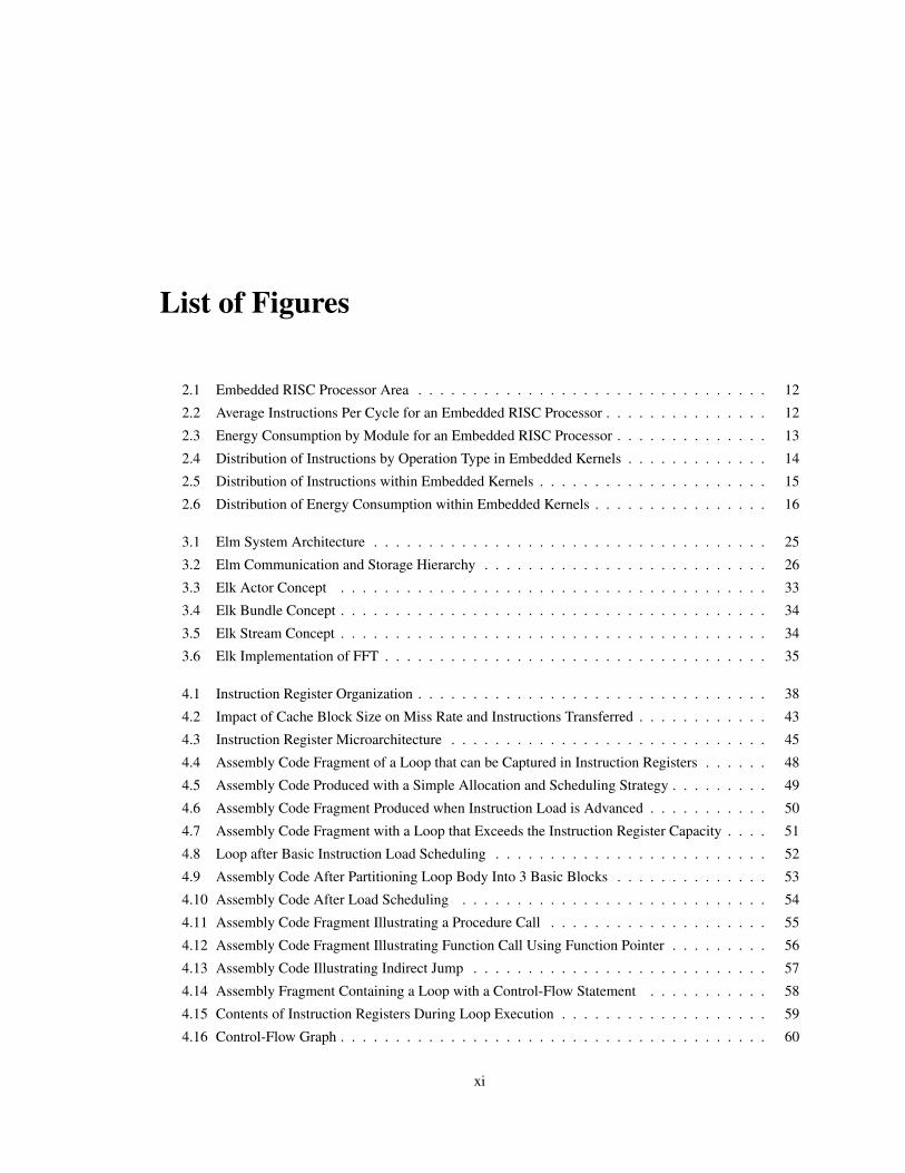
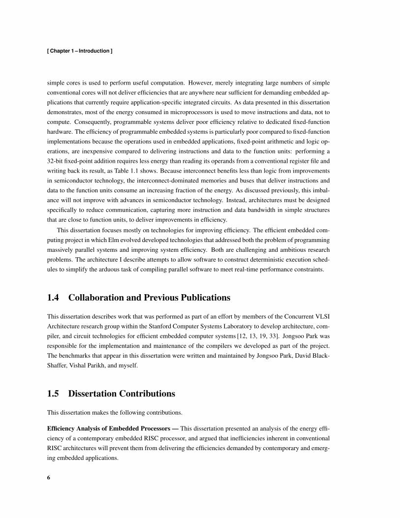
Figure 2.1 shows the area occupied by the processor. The entire design occupies a region that is about 0.5 mmby 0.3 mm. The area reported is measured after the design is placed and routed. As the data presented in thefigure clearly illustrate, despite the relative simplicity of the architecture and implementation, the processorarea is dominated by circuits that are used to stage instructions and data. The integer core contributes 22.5%of the area, the register file 11.0%, and the instruction and data caches contribute the remaining 66.6%. About53% of the standard cell area in the integer core is contributed by flip-flops and latches, most of which areused to coordinate the movement of instructions to the function units and to stage operands and results. Thetag and data arrays are implemented as high-density SRAM modules that are compiled and provided by thefoundry. Despite the density and small capacities of the arrays, the area of the caches is dominated by the tagand data arrays, which consume 56.3% of the entire area. The cache and memory controllers occupy about15.4% of the cache area.
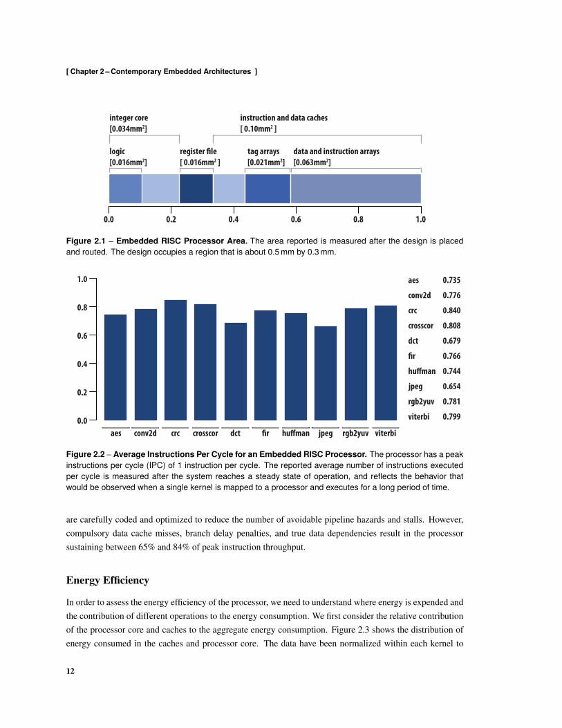
To evaluate the area efficiency, we need to account for the rate at which the processor completes ap-plication work. The number of instructions executed per cycle (IPC) provides a reasonable estimate of theeffective processor utilization, though it does not account for how efficiently application operations may bemapped to the processor operations exposed by the instruction set. Figure 2.2 shows the average numberof instructions executed per cycle for several common embedded kernels. The kernels are described in de-tail in Appendix A. The reported data were measured after the persistent instruction and data working setsare captured in the caches; any loss of performance due to cache misses is introduced by compulsory datamisses. The processor has a peak instruction execution rate of one instruction per cycle, and the kernels
11
[ Chapter 2 – Contemporary Embedded Architectures ]
instruction and data caches[ 0.10mm2 ]
integer core [0.034mm2]
register !le[ 0.016mm2 ]
logic [0.016mm2]
tag arrays[0.021mm2]
data and instruction arrays [0.063mm2]
0.0 0.2 0.4 0.6 0.8 1.0
Figure 2.1 – Embedded RISC Processor Area. The area reported is measured after the design is placedand routed. The design occupies a region that is about 0.5 mm by 0.3 mm.
aes conv2d crc crosscor dct !r hu"man jpeg rgb2yuv viterbi0.0
0.2
0.4
0.6
0.8
1.0
conv2d 0.776
aes 0.735
crc 0.840
0.808crosscor
0.679dct
0.766!r
0.744hu"man
0.654jpeg
0.781rgb2yuv
0.799viterbi
Figure 2.2 – Average Instructions Per Cycle for an Embedded RISC Processor. The processor has a peakinstructions per cycle (IPC) of 1 instruction per cycle. The reported average number of instructions executedper cycle is measured after the system reaches a steady state of operation, and reflects the behavior thatwould be observed when a single kernel is mapped to a processor and executes for a long period of time.
are carefully coded and optimized to reduce the number of avoidable pipeline hazards and stalls. However,compulsory data cache misses, branch delay penalties, and true data dependencies result in the processorsustaining between 65% and 84% of peak instruction throughput.
Energy Efficiency
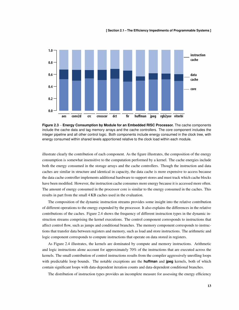
In order to assess the energy efficiency of the processor, we need to understand where energy is expended andthe contribution of different operations to the energy consumption. We first consider the relative contributionof the processor core and caches to the aggregate energy consumption. Figure 2.3 shows the distribution ofenergy consumed in the caches and processor core. The data have been normalized within each kernel to
12
[ Section 2.1 – The Efficiency Impediments of Programmable Systems ]
aes conv2d crc crosscor dct !r hu"man jpeg rgb2yuv viterbi0.0
0.2
0.4
0.6
0.8
1.0
core
datacache
instructioncache
Figure 2.3 – Energy Consumption by Module for an Embedded RISC Processor. The cache componentsinclude the cache data and tag memory arrays and the cache controllers. The core component includes theinteger pipeline and all other control logic. Both components include energy consumed in the clock tree, withenergy consumed within shared levels apportioned relative to the clock load within each module.
illustrate clearly the contribution of each component. As the figure illustrates, the composition of the energyconsumption is somewhat insensitive to the computation performed by a kernel. The cache energies includeboth the energy consumed in the storage arrays and the cache controllers. Though the instruction and datacaches are similar in structure and identical in capacity, the data cache is more expensive to access becausethe data cache controller implements additional hardware to support stores and must track which cache blockshave been modified. However, the instruction cache consumes more energy because it is accessed more often.The amount of energy consumed in the processor core is similar to the energy consumed in the caches. Thisresults in part from the small 4 KB caches used in the evaluation.
The composition of the dynamic instruction streams provides some insight into the relative contributionof different operations to the energy expended by the processor. It also explains the differences in the relativecontributions of the caches. Figure 2.4 shows the frequency of different instruction types in the dynamic in-struction streams comprising the kernel executions. The control component corresponds to instructions thataffect control flow, such as jumps and conditional branches. The memory component corresponds to instruc-tions that transfer data between registers and memory, such as load and store instructions. The arithmetic andlogic component corresponds to compute instructions that operate on data stored in registers.
As Figure 2.4 illustrates, the kernels are dominated by compute and memory instructions. Arithmeticand logic instructions alone account for approximately 70% of the instructions that are executed across thekernels. The small contribution of control instructions results from the compiler aggressively unrolling loopswith predictable loop bounds. The notable exceptions are the huffman and jpeg kernels, both of whichcontain significant loops with data-dependent iteration counts and data-dependent conditional branches.
The distribution of instruction types provides an incomplete measure for assessing the energy efficiency
13

[ Chapter 2 – Contemporary Embedded Architectures ]
aes conv2d crc crosscor dct !r hu"man jpeg rgb2yuv viterbi0.0
0.2
0.4
0.6
0.8
1.0
arithmeticandlogic
memory
control
Figure 2.4 – Distribution of Instructions by Operation Type in Embedded Kernels. The control componentincludes control flow instructions, the preponderance of which are conditional branches and jump instructions.The memory component includes data transfer instructions that access memory, which are almost exclusivelyload and store instructions. The arithmetic and logic component includes all arithmetic and logic instructions,which are dominated by integer arithmetic and logic operations. The processor implements a multiply-and-accumulate instruction, which encodes two basic arithmetic operations. The multiply-and-accumulate instruc-tion is used extensively in the arithmetically intensive kernels.
of the processor because it does not account for how different instructions contribute to the computationdemanded by the kernels. Many of the arithmetic and logic instructions encode operations that are notfundamental to the kernels, but a consequence of their implementation. For example, arithmetic and logicinstructions may appear in instruction sequences that implement control and memory access operations thatcannot be encoded directly in the instruction set. Data references and control statements in programminglanguages often map to sequences of instructions. For example, a compiler may map an effective addresscalculation to an instruction sequence comprising an arithmetic instruction followed by a load instruction. Itis important that we differentiate operations that are fundamental to a computation from computations thatare a consequence of the architecture a computation is mapped to.
To asses correctly the impact of the processor architecture on its energy efficiency, we implemented acompiler data flow analysis to classify instructions as control and memory operations based on how the val-ues the instructions compute are used rather than the operations instructions perform. The data flow analysiscan analyze assembly code listings produced by other compilers. It uses the results of a reaching defini-tions analysis to propagate data flow information backwards from control flow and memory instructions.The reaching definitions analysis follows variables that are stack allocated and temporarily spilled and re-stored during a procedure invocation through spills and restores to fixed memory locations. The analysisidentifies instructions that compute condition operands to control flow operations and address operands tomemory operations. The analysis propagates data flow information backwards through arithmetic and logicinstructions to identify sets of dependent arithmetic and logic instructions that compute control and address
14

[ Section 2.1 – The Efficiency Impediments of Programmable Systems ]
aes conv2d crc crosscor dct !r hu"man jpeg rgb2yuv viterbi0.0
0.2
0.4
0.6
0.8
1.0
compute
memory
control
Figure 2.5 – Distribution of Instructions within Embedded Kernels. The control component includes con-trol flow instructions and those arithmetic and logic instructions that compute operands to control flow instruc-tions. The memory component includes data transfer instructions that access memory and those arithmeticand logic instructions that provide address operands to data transfer instructions. The compute componentincludes arithmetic and logic instructions that implement computations demanded by the kernels. An arith-metic or logic instruction that defines a value that is both fundamental to the computation of a kernel and usedby a control or memory operation is designated a compute instruction. An arithmetic or logic instruction thatdefines a value that is an operand to both a control and memory operation is designated a control instruction.
operands. Arithmetic and logic instructions that define values that are used exclusively as condition andaddress operands or exclusively to compute condition and address operands are classified as control andmemory operations.
The results of the analysis appear in Figure 2.5. The data illustrated in the figure provide a more detailedaccounting of the composition of the instructions comprising the kernels. Compute operations are encodedin 53% of the instructions on average. The crosscor kernel is dominated by memory operations, and only32% of its instructions encode compute operations. The rgb2yuv kernel has very simple control and smalldata working sets that the compiler maps to the register file, and 77% of its instructions encode computeoperations.
To assess the energy efficiency of the processor, we also need to account for the impact of microarchi-tecture on the energy consumed in the processor core. A significant component of the energy expended inthe processors is used to deliver operands to function units and control signals decoded from instructions todata-path control points. Though necessary to execute instructions, such energy is an overhead imposed bythe programmability afforded by the architecture.
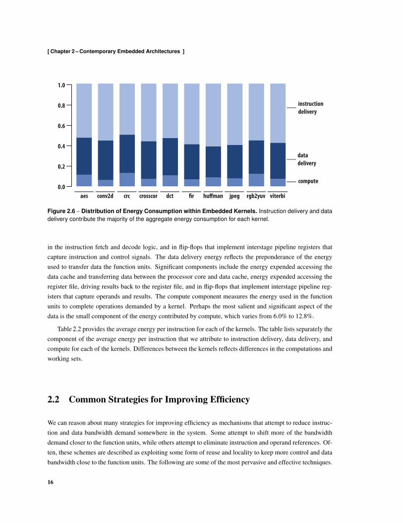
Figure 2.6 shows a detailed analysis of the contribution of instruction delivery, data delivery, and computeto the aggregate energy consumption of each kernel. The instruction delivery energy reflects the preponder-ance of the energy used to deliver instructions to the data-path control points. Significant components includethe energy used to access the instruction cache and transfer instructions to the processor, energy expended
15
[ Chapter 2 – Contemporary Embedded Architectures ]
aes conv2d crc crosscor dct !r hu"man jpeg rgb2yuv viterbi0.0
0.2
0.4
0.6
0.8
1.0
compute
datadelivery
instructiondelivery
Figure 2.6 – Distribution of Energy Consumption within Embedded Kernels. Instruction delivery and datadelivery contribute the majority of the aggregate energy consumption for each kernel.
in the instruction fetch and decode logic, and in flip-flops that implement interstage pipeline registers thatcapture instruction and control signals. The data delivery energy reflects the preponderance of the energyused to transfer data the function units. Significant components include the energy expended accessing thedata cache and transferring data between the processor core and data cache, energy expended accessing theregister file, driving results back to the register file, and in flip-flops that implement interstage pipeline reg-isters that capture operands and results. The compute component measures the energy used in the functionunits to complete operations demanded by a kernel. Perhaps the most salient and significant aspect of thedata is the small component of the energy contributed by compute, which varies from 6.0% to 12.8%.
Table 2.2 provides the average energy per instruction for each of the kernels. The table lists separately thecomponent of the average energy per instruction that we attribute to instruction delivery, data delivery, andcompute for each of the kernels. Differences between the kernels reflects differences in the computations andworking sets.
2.2 Common Strategies for Improving Efficiency
We can reason about many strategies for improving efficiency as mechanisms that attempt to reduce instruc-tion and data bandwidth demand somewhere in the system. Some attempt to shift more of the bandwidthdemand closer to the function units, while others attempt to eliminate instruction and operand references. Of-ten, these schemes are described as exploiting some form of reuse and locality to keep more control and databandwidth close to the function units. The following are some of the most pervasive and effective techniques.
16

[ Section 2.2 – Common Strategies for Improving Efficiency ]
aes conv2d crc crosscor dct fir huffman jpeg rgb2yuv viterbi
Instruction 34.9 33.2 30.3 32.2 37.7 34.0 35.4 39.9 32.8 32.5Data 23.9 23.0 22.8 21.2 26.1 19.8 17.7 21.85 19.5 19.9Compute 7.4 3.6 7.9 4.1 7.5 3.9 4.9 5.0 7.2 4.1
66.2 59.8 61.0 57.5 71.3 57.7 58.0 66.7 59.4 56.5Other 5.6 7.5 5.3 6.7 13.5 6.2 8.1 21.0 11.7 12.3
Total 71.8 67.3 66.3 64.2 84.8 63.9 66.1 87.0 71.1 68.7
Table 2.2 – Average Energy Per Instruction for an Embedded RISC Processor. The energy is reported inpicojoules and is computed by averaging over all of the instructions comprising a kernel. The average energyper instruction captures the energy consumed performing the computation that is fundamental to a kernel,energy consumed transferring instructions and data to function units, and energy consumed orchestrating themovement of instructions and data. The Instruction row lists the energy that is consumed delivering instructionsto the function unit. The Data row lists the energy consumed delivering data to the function unit. The Computerow lists the energy consumed in the function units to execute those instructions that perform operations thatare intrinsic to a kernel, as opposed to those operations that are executed to coordinate the movement andsequencing of instructions and data. The Other row lists energy contributed by when the processor is stalled.Mechanisms such as leakage current and activity in the clock network when the processor is stalled contributea significant component of the average energy per instruction. Most of the flip-flops in the design are clock-gated, and consequently there is little activity near the leaf elements when the processor is stalled; however,nodes near the root of the clock tree have the largest capacitance of any nodes in the processor design andhave the highest activity factors.
Exploit Locality to Reduce Data and Instruction Access Energy
We can exploit locality in instruction and operand accesses to improve energy efficiency. Typically, thisentails using register organizations that keep operands close to function units, and using memory hierarchiesthat exploit reuse and locality to capture important instruction and data working sets close to processors.These organizations usually use small structures to reduce access energies and distribute storage structuresclose to function units to reduce communication and transport energies.
Amortize Instruction Fetch and Control
We can use single-instruction multiple-data (SIMD) architectures to reduce instruction bandwidth when ap-plications exhibit regular data-level parallelism. Traditional vector processors improve efficiency by amortiz-ing instruction fetch and decode energy by applying an instruction to multiple operands [59]. Many modernarchitectures provide collections of sub-word SIMD instructions that apply an operation to multiple operandsthat are packed in a common register. These schemes also eliminate or amortize the dependency checks thatare required to determine when an operation may be initiated safely, which effectively reduces demand forcontrol hardware bandwidth.
17
[ Chapter 2 – Contemporary Embedded Architectures ]
Use Simple Control and Decode Hardware
Most commercial embedded processors use simple hardware architectures to improve area and power effi-ciency. Many use RISC architectures that offer simple control and decode hardware. High-end digital signalprocessors often use VLIW architecture to efficiently exploit instruction-level parallelism found in many tra-ditional signal processing algorithms [43]. These systems rely on compiler technology rather than hardwareto discover and exploit instruction-level parallelism, and are able to scale to very wide issue. Many rely onpredication to conditionally execute instructions to expose sufficient instruction-level parallelism. TraditionalVLIW processors suffer from poor instruction density and large code sizes. Digital signal processors that useVLIW architectures rely on sophisticated instruction compression and packing schemes to eliminate the needfor explicit no-ops and improve code sizes.
Exploit Operation-Level Parallelism with Compound Instructions
We can reduce the number of instructions that need to be executed to implement a computation by exploitingoperation-level parallelism and encoding multiple simple dependent operations as a single machine instruc-tion. For example, many modern architectures provide fused multiple-add instructions that encode a multipli-cation operation and a dependent addition operation. Like the instruction bundles used to encode independentinstructions in VLIW architectures, compound instructions encode multiple arithmetic and logic operations;unlike instruction bundles, which encode multiple independent operations, compound instructions usuallyencode dependent operations.
Many architectures fuse short sequences of simple instructions into compound instructions to improveperformance and reduce instruction bandwidth and energy. These can be common compound arithmeticoperations that are provided by the hardware and selected by a compiler [105, 71]. They may be constructedby configuring stages in a function unit. For example, a processor could allow software to configure the stagethat implements different rounding and saturating arithmetic mode[10]. They may rely on a combinationof compiler analysis and hardware mechanisms for dynamically configuring a cluster of simple functionunits [23].
As with VLIW architectures, there is a limited number of useful operations that can be performed withoutadditional register file bandwidth to deliver more operands to the compound instructions. The additionalcontrol logic, multiplexers, pipeline registers required by the additional function units, and the increasedinterconnect distances between the register file and function units that must be traversed increase the expenseof executing simple instructions.
Exploit Application-Specific Instructions
We can provide instructions that implement highly stereotyped application-specific operations as sequencesof dedicated instructions to reduce instruction and operand fetch bandwidth. Commercial digital signalprocessors often implement application-specific instructions to accelerate core kernels in important sig-nal processing algorithms. For example, some digital signal processors for mobile applications provide
18
[ Section 2.2 – Common Strategies for Improving Efficiency ]
instructions that perform domain-specific operations, such as compare-select-max-and-store and square-distance-and-accumulate [140], to accelerate specific baseband processing algorithms in cellular telephoneapplications. Extensible processor architectures such as the Xtensa processor cores designed by Tensilicaallow custom application-specific instructions to be introduced to a load-store instruction set architectureat design time [53]. A more aggressive example, recent TriMedia media processors implement complexsuper-instructions that issue across multiple VLIW instruction slots and function units [143]. The super-instructions implement specific operation that are used in the context-based adaptive binary arithmetic codingscheme used in advanced digital video compression standards. These super-instructions essentially embeddedapplication-specific fixed function hardware in the function units.
The complex behaviors encoded by application-specific instructions can make it difficult for compilersto use application-specific instructions effectively, as the compiler must be designed to expose and identifyclusters of operations that can be mapped to application-specific instructions. The problem is more acutewhen applications-specific instructions use unconventional data types and operands widths. Consequently,important application codes that can benefit from application-specific instructions often must be manuallymapped to assembly instructions.
Switch to Multicore Architectures
Multicore architectures integrate multiple processor cores in a system-on-chip [112]. As microprocessor de-signs became increasingly more complex, using the additional transistors provided by technology scalingto implement multiple simple cores required considerably less engineering effort than attempting to design,implement, and verify increasingly more aggressive and complex speculative superscalar out-of-order proces-sors [56]. Multicore architectures consciously prefer improved aggregate system performance to improvedsingle-thread performance [5], and most multicore processors use increasing transistor budgets to exploitthread-level parallelism rather than instruction-level parallelism [15]. Because power dissipation constraintsand wire delays limit the performance and efficiency of complex processors, almost all processor designs haveshifted to a paradigm in which new processors provide more cores [127, 125, 144, 92, 8, 124], deliver modestmicroarchitecture improvements to increase single-thread performance and power efficiency [144, 92], andsupport additional thread-level parallelism within cores [97, 108]. To further improve energy efficiency, con-temporary designs implement dynamic voltage and frequency scaling schemes [21] that allow single threadperformance to be reduced in exchange for greater energy efficiency [55, 92]
Exploit Voltage Scaling and Parallelism
We can exploit voltage scaling to improve energy efficiency in applications with task-level and data-levelparallelism by mapping parallel computation across multiple processors [153, 22]. The basic idea is to useparallelism to exploit the quadratic dependence of energy on supply voltage in digital circuits [21]. If weignore the overheads of task and data distribution and communication, mapping parallel computation acrossmultiple processors results in a linear increase in area and switched capacitance. In exchange, we can lowerthe supply voltage to produce a quadratic reduction in the dynamic energy per operation. As we should
19

[ Chapter 2 – Contemporary Embedded Architectures ]
expect, there are limits. Physical design considerations and constraints such as power supply noise anddevice variation often limit the extent to which supply voltages can be lowered reliably. Many circuits,such as conventional static random access memory cells, have a minimum supply voltage below which theywill not operate reliably. Eventually, minimum supply voltage constraints, decreasing efficiency gains, orincreasing circuit delays that may not be acceptable in latency-sensitive systems limit the extent to whichvoltage scaling can be used to improve efficiency. Furthermore, most consumer applications are cost sensitive,and the reduction in clock frequency and accompanying degradation in area efficiency result in what are oftenunacceptable increases in silicon and packaging costs.
Devise Manycore Architectures
The terms manycore and massively multicore are often used to refer to multicore architectures with tens tohundreds of cores. This definition is somewhat problematic because process scaling allows the number ofcores in a multicore architecture to increase steadily. Multicore effectively describes architectures descendedfrom single processors through processes in which the number of standard processor cores per die essen-tially doubles when a new semiconductor process generation doubles transistor densities [11]. Perhaps theterm manycore distinguishes scalable architectures designed specifically to improve application performanceand efficiency by distributing parallel computations across large numbers of highly integrated cores. Thesearchitectures often rely on explicitly parallel programming models to expose sufficient parallelism.
Mancycore architectures are specifically designed to exploit data-level and task-level parallelism withinapplications. They focus on delivering massive numbers of function units efficiently, and support massiveamounts of parallelism. Unlike the communication primitives found in multicore processors, which descendfrom architectures designed to support multi-chip multiprocessors typically comprising from 2 to 16 proces-sors, manycore architectures integrate scalable communication systems that exploit the low communicationlatencies and abundant communication bandwidth that are available on chip. Consequently, manycore ar-chitectures deliver significantly more arithmetic bandwidth than multicore processors, and usually achievesuperior area and energy efficiency when handling applications with sufficient structure and locality. How-ever, the ability of tiled manycore architectures that use conventional RISC microprocessors and digital signalprocessors [139, 52, 14, 46, 54, 153] to improve efficiency is limited by the efficiency of the processors fromwhich they are constructed: tiling provides additional function units, which increases throughput, but doesnot improve the architectural efficiency of the individual cores.
2.3 A Survey of Related Contemporary Architectures
Data parallel architectures such as the Stanford Imagine processor [121], the MIT Scale processor [88], andNVIDIA graphics processors [99] amortize instruction issue and control overhead by issuing the same in-struction to multiple parallel function units. However, the efficiency of data parallel architectures deteriorateswhen applications lack sufficient regular data parallelism. Sub-word SIMD architectures that use mecha-nisms such as predicate masks to handle divergent control flow [106, 98, 128] perform particularly poorly
20

[ Section 2.3 – A Survey of Related Contemporary Architectures ]
when applications lack adequate regular data parallelism because multiple control paths must be executedand operations discarded [135, 73]. The following sections discuss in detail several architectures that arerepresentative of alternative efficient embedded and application-specific processor architectures.
MIT Raw and Tilera TILE Processors
The MIT Raw processor is perhaps the canonical example of a tiled multicore processor. The Raw processorcomprises 16 simple RISC cores connected by multiple mesh networks [137]. The Raw architecture exposeslow-level computation, storage, and communication resources to software, and relies on compiler technol-ogy to efficiently map computations onto hardware [147]. The Raw architecture exposes software-scheduledscalar operand networks that are tightly coupled to the function units for routing operands between tiles [138].The Raw architecture was designed to exploit instruction-level parallelism; its architects designed the archi-tecture to scale beyond what were considered to be communication limitations of conventional superscalararchitectures by exposing wire delays and distributed resources directly to software [139]. The Raw compilermodels the machine as a distributed register architecture and attempts to map the preponderance of com-munication between function units onto these scalar operand networks using compiler technologies such asspace-time scheduling of instruction-level parallelism [96]. The Raw architecture was better able to exploittask-level and data-level parallelism than instruction-level parallelism, and could be effectively programmedusing stream programming languages such as StreamIt [141, 75, 49].
The Tilera TILE architecture is the commercial successor to the MIT Raw architecture. The TILE64processor is a system-on-chip with 64 conventional 3-wide VLIW cores that are connected by multiple meshnetworks [18]. The TILE processor architecture adds support for sub-word SIMD operations, which improvethe performance of various video processing applications that process 8-bit and 16-bit data. The TILE ar-chitecture provides both software-routed scalar operand networks and general-purpose dynamically routednetworks, and retains the ability to send data directly from registers and receive data in registers when com-munication is mapped to the software-controlled networks [148]. To decouple the order in which messagesare received from the order in which software processes the messages, the software-controlled networks im-plement multiple queues and allow messages to be tagged for delivery to a specific queue. A shared SRAMstores messages at the receiver, and small dedicated per-flow hardware queues provide direct connectionsto the function units [18]. The scalar operand networks improve the efficiency at which fine-grain pipeline-parallelism and task-parallelism can be mapped to the architecture.
Berkeley VIRAM Vector Processor
The Berkeley VIRAM processor is a vector processor that uses embedded DRAM technology to implementa processor-in-memory. Like conventional vector processors, VIRAM has a general-purpose scalar controlprocessor and a vector co-processor. It implements 4 64-bit vector lanes and a hardware vector length of32 [84]. The architecture allows instructions to operate on sub-word SIMD operands within each lane, whichincreases the effective vector length of the machine when operating on packed data elements. When suf-ficient regular data-level parallelism is available in a loop, increasing the vector length reduces instruction
21

[ Chapter 2 – Contemporary Embedded Architectures ]
bandwidth, as a single vector instruction is applied to more elements. To allow data-parallel loops that con-tain control-flow statements to be mapped to the vector units, the VIRAM instruction set architecture includesvector flags, compress, and expand operations to support conditional execution.
Stanford Imagine and SPI Storm Stream Processors
Stream processors are optimized to exploit the regular data-level parallelism found in signal processing andmultimedia applications [81, 74, 35]. Like vector processors, stream processor architectures have a scalarcontrol processor that issues commands to a co-processor comprising a collection of data-parallel executionunits. Stream applications are expressed as computation kernels that operate on streams of data. The kernelsare compute-intensive functions that operate on data streams, and usually correspond to the critical loops inan application. The data streams are sequences of records. The data stream construct makes communicationbetween kernels explicit, which greatly simplifies the compiler analysis that are required to perform codetransformations that improve data reuse and locality. The control processor coordinates the movement of databetween memory and the data-parallel execution units, and launches kernels that execute on the data-parallelexecution units. Stream memory operations transfer data between memory and a large stream register file thatstages data to and from the data-parallel units. Stream processors differ most significantly from conventionalvector architectures in their use of software-managed memory hierarchies to allow software to explicitlycontrol the staging of stream transfers through the memory hierarchy [121]. The storage hierarchy allowsintra-kernel reuse and locality to be captured in registers, and inter-kernel locality to be captured in a largeon-chip stream register file. The stream register file is also used to stage large bulk data transfers betweenDRAM and registers. The capacity of the stream register file allows it to be used to tolerate long memoryaccess times. Irregular data-level parallelism requires the use of techniques such as conditional streams toallow arbitrary stream expansion and stream compression in space and time [73].
The Stanford Imagine processor has 8 data-parallel lanes, each of which has 7 function units [81]. Imagineuses a micro-sequencer to coordinate the sequencing of kernel invocations and issuing of the instructionscomprising a kernel to the data-parallel units, which decouples the launching of a kernel on the controlprocessor from the execution of the data-parallel units. This differs somewhat from conventional vectorprocessors that issue individual vector instructions in order to the vector unit [10]. The function units withina lane allow Imagine to exploit instruction-level parallelism, and the multiple lanes allow Imagine to exploitSIMD data-level parallelism. The SPI Storm-1 processor is the commercial successor to Imagine. It integratesthe control processor on the same chip as the data-parallel execution units, and increases the number of data-parallel lanes from 8 to 16 [80].
MIT Scale Processor
The MIT Scale vector-thread processor supports both vector and multithreaded processing. It implements avector-thread architecture in which a control thread executes on a control processor and issues instructionsto a collection of micro-threads that execute concurrently on parallel vector lanes [88]. The control threadallows common control and memory operations to be factored out of the instruction streams that are issued
22
[ Section 2.4 – Chapter Summary ]
to the micro-threads, which allows regular control-flow and data accesses to be handled efficiently. Thecontrol processor issues vector fetch instruction to dispatch blocks of instructions to the micro-threads. Thearchitecture allows micro-threads to execute independent instruction streams, which improves the handlingof irregular data-parallel applications. For example, the micro-threads may diverge after executing scalarbranches contained in a block of instructions that were dispatched from a vector fetch command. To supportdivergent micro-thread execution, the Scale processor provisions more instruction fetch bandwidth than aconventional vector processor would. The Scale processor implements a clustered function unit organizationthat supports 4-wide VLIW execution within each vector lane [87], which allows it to exploit well structuredinstruction-level parallelism. To reduce the amount of hardware and miss state required to sustain the largenumber of in-flight memory requests that are generated, Scale implements a vector refill unit that pre-executesvector memory operations and issues any needed cache line refills ahead of regular execution [17].
Illinois Rigel Accelerator
The Illinois Rigel Accelerator is a programmable accelerator architecture that emphasizes support for data-parallel and task-parallel computation [77]. It provides a collection of simple cores and hierarchical caches,and emphasizes support for single-program multiple-data models of computation. The memory hierarchy hastwo levels: a local cluster cache that is shared by 8 processors, and a distributed collection of global cachebanks that are associated with off-chip memory interfaces. To simplify the mapping of applications to theaccelerator, the programming model structures computation as collections of parallel tasks. Interprocessorcommunication uses shared memory and is implicit. The programming system provides a cached global ad-dress space, and relies on a software memory coherence scheme to reduce communication overhead. Explicitsynchronization instructions are provided to allow the runtime system to implement barriers, and to acceleratethe enqueuing and dequeuing tasks from distributed work queues. The instruction set architecture exposesmechanisms that support implicit locality management, such as load and store instructions that specify wheredata may be cached. The memory consistency model provides coherence at a limited number of well-definedpoints within an application, and relies on software to enforce the cache coherence protocol [78].
2.4 Chapter Summary
This chapter presented an analysis of efficiency of a simple embedded RISC processor that provides a reason-able approximation of an efficient modern embedded processor. The analysis reveals that the preponderanceof the energy consumed in the processor is used to transfer instructions and data to function units, not to com-pute. This result explains and quantifies the significant disparities between the efficiencies of programmableprocessors and application-specific fixed-function hardware. It also implies a limit to the efficiencies thatcan be achieved using conventional processor architectures in manycore systems. Mapping parallel compu-tations to collections microprocessors and digital signal processors provides additional function units, whichimproves throughput, but does not improve the architectural efficiencies of the cores. As a consequence,aggregate system efficiency will ultimately be limited by the efficiency of the individual processor cores.
23
Chapter 3
The Elm Architecture
This chapter introduces the Elm architecture. It motivates and develops important concepts that informed thedesign of Elm, and presents many of the ideas that are developed in subsequent chapters.
3.1 Concepts
Embedded applications have abundant task-level and data-level parallelism, and there is often considerableoperation-level parallelism within tasks. Components of embedded systems such as application-specific inte-grated circuits exploit this abundant parallelism by distributing computation over many independent functionunits; both performance and efficiency improve because instructions and data are distributed close to func-tion units. Efficiency is further improved by exploiting extensive reuse and producer-consumer locality inembedded applications. Individual components in embedded systems tend to perform the same computationrepeatedly, which is why they can benefit from fixed-function logic. This behavior may be used to exposeextensive instruction and data reuse.
Programmability allows tasks to be time-multiplexed onto collections of function units, which both im-proves area efficiency and energy efficiency. Systems that use special-purpose fixed-function logic usuallyprovision dedicated hardware for each application and tasks. Depending on application demand, some fixed-function hardware will be idle, resulting in resource underutilization and poor area efficiency. For example,cellular telephone handsets that support multiple wireless protocols typically implement multiple basebandprocessing blocks even though multiple blocks cannot be used concurrently. Time multiplexing tasks ontoprogrammable hardware allows a collection of function units to implement different applications and differ-ent tasks within applications as demanded by the system. Programmability improves energy efficiency whendata communication dominates by allowing tasks to be dispatched to data. Rather than requiring that data betransferred to and from hardware capable of implementing some specific task, the task may be transferred tothe data, reducing data communication and aggregate instruction and data bandwidth demand.
24
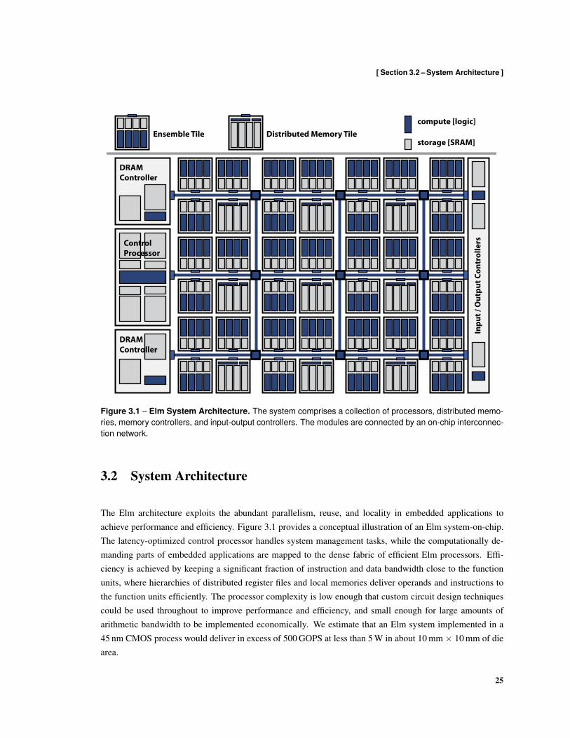
[ Section 3.2 – System Architecture ]
DRAMController
DRAMController
ControlProcessor
Inpu
t / O
utpu
t Con
trol
lers
Ensemble Tile Distributed Memory Tilecompute [logic]
storage [SRAM]
Figure 3.1 – Elm System Architecture. The system comprises a collection of processors, distributed memo-ries, memory controllers, and input-output controllers. The modules are connected by an on-chip interconnec-tion network.
3.2 System Architecture
The Elm architecture exploits the abundant parallelism, reuse, and locality in embedded applications toachieve performance and efficiency. Figure 3.1 provides a conceptual illustration of an Elm system-on-chip.The latency-optimized control processor handles system management tasks, while the computationally de-manding parts of embedded applications are mapped to the dense fabric of efficient Elm processors. Effi-ciency is achieved by keeping a significant fraction of instruction and data bandwidth close to the functionunits, where hierarchies of distributed register files and local memories deliver operands and instructions tothe function units efficiently. The processor complexity is low enough that custom circuit design techniquescould be used throughout to improve performance and efficiency, and small enough for large amounts ofarithmetic bandwidth to be implemented economically. We estimate that an Elm system implemented in a45 nm CMOS process would deliver in excess of 500 GOPS at less than 5 W in about 10 mm × 10 mm of diearea.
25
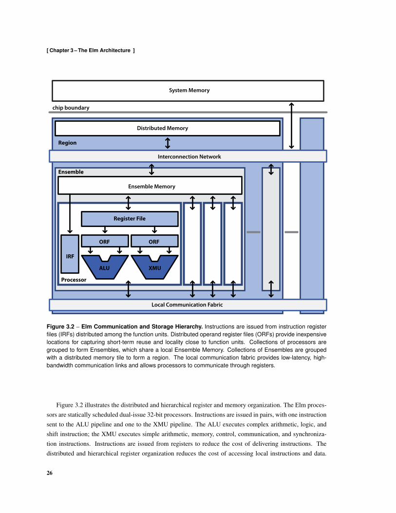
[ Chapter 3 – The Elm Architecture ]
Interconnection Network
Distributed Memory
Ensemble Memory
Local Communication Fabric
System Memory
ORF ORF
Register File
IRF
chip boundary
Ensemble
Region
Processor
ALU XMU
Figure 3.2 – Elm Communication and Storage Hierarchy. Instructions are issued from instruction registerfiles (IRFs) distributed among the function units. Distributed operand register files (ORFs) provide inexpensivelocations for capturing short-term reuse and locality close to function units. Collections of processors aregrouped to form Ensembles, which share a local Ensemble Memory. Collections of Ensembles are groupedwith a distributed memory tile to form a region. The local communication fabric provides low-latency, high-bandwidth communication links and allows processors to communicate through registers.
Figure 3.2 illustrates the distributed and hierarchical register and memory organization. The Elm proces-sors are statically scheduled dual-issue 32-bit processors. Instructions are issued in pairs, with one instructionsent to the ALU pipeline and one to the XMU pipeline. The ALU executes complex arithmetic, logic, andshift instruction; the XMU executes simple arithmetic, memory, control, communication, and synchroniza-tion instructions. Instructions are issued from registers to reduce the cost of delivering instructions. Thedistributed and hierarchical register organization reduces the cost of accessing local instructions and data.
26
[ Section 3.2 – System Architecture ]
The Elm processors use block instruction and data transfers to improve the efficiency of transferring instruc-tions and data between registers and memory.
The processors communicate over an on-chip interconnection network and a distributed local commu-nication fabric. The memory and communication systems near the processors provide predictable latenciesand bandwidth to simplify the process of compiling to real-time performance and efficiency constraints. Thecompute, memory, and communication resources are exposed to software to provide fine-grain control overhow computation unfolds, and the programming systems and compiler may explicitly orchestrate instructionand data movement. The result is that the complexity and expense of developing large embedded systems isin the development of compilers and programming tools, the cost of which is amortized over many systems,rather than in the design and verification of special-purpose fixed-function hardware which must be paid forin each new system.
Ensembles
Clusters of four processors are grouped into Ensembles, the primary physical design unit for compute re-sources in an Elm system. The processors in an Ensemble are loosely coupled, and share local resources suchas a pool software-managed memory and an interface to the interconnection network. The Ensemble organi-zation is exposed to software, and the software concept of an Ensemble provides a metaphor for describingand encoding spatial locality among the processors within an Ensemble.
The Ensemble memory captures instruction and data working sets close to the processors, and is banked toallow the local processors and network interface controller to access it concurrently. The compiler can exploittask-level parallelism by executing parallel tasks on the processors in an Ensemble, capturing fine-grainproducer-consumer data locality within the Ensemble to improve efficiency. Reuse among the processorsreduces the demand for instruction and data bandwidth outside the Ensemble. For example, executing paralleliterations of a loop on different processors in an Ensemble increases performance by exploiting data-levelparallelism; amortizing the cost of moving the instruction and data to Ensemble memory increases efficiencyby exploiting instruction and data reuse across iterations.
Remote memory accesses are performed over the on-chip interconnection network. The Ensemble mem-ory can be used to stage transfers. Hardware at the network interface supports bulk memory operations toassist the compiler in scheduling proactive instruction and data movements to hide remote memory accesslatencies. The Ensemble organization effectively concentrates interconnection network traffic at Ensembleboundaries and allows multiple processors share a network interface and the associated connection to thelocal router. This amortizes the network interface and network connection across multiple processors, whichprovides an important improvement in area efficiency because the processors are relatively small.
The local communication fabric connects the processors in an Ensemble with high-bandwidth point-to-point links. The fabric can be used to capture predictable communication, and allows the compiler tomap instruction sequences across multiple processors. The fabric can also be used to stream data betweenEnsembles deterministically at low latencies. The fabric is statically routed, and avoids the expense cyclinglarge memory arrays incurs when communicating through memory.
27
[ Chapter 3 – The Elm Architecture ]
Efficient Instruction Delivery
Elm uses compiler-managed instruction registers (IRs) to store instructions close to function units. Instruc-tions are issued directly from instruction registers. Instruction registers keep a significant fraction of theinstruction bandwidth close to the function units by capturing reuse and locality within loops and kernels.The instruction registers are organized as shallow instruction register files (IRFs) that are located close to thefunction units. The register files are fast and inexpensive to access, and their proximity to the function unitsreduces the energy required to transfer instructions to the datapaths. The shallow register files require fewbits to address, allowing a short instruction counter (IC) to be used instead of a conventional program counter.An IC is less expensive to maintain, which reduces the energy consumed coordinating instruction issue andtransfers of control. The contents of the instruction registers and the instruction counter implicitly definethe state captured by a program counter. A complete set of control-flow instructions is implemented, andarbitrary transfers of control are permitted, provided that the target instruction resides in a register. Relativetarget addresses are resolved while instructions are loaded to improve efficiency: the hardware that resolvesrelative targets is active only when instructions are being loaded.
The instruction registers are backed by the Ensemble memory. The compiler explicitly orchestrates themovement of instructions into registers by scheduling instruction loads. An instruction load moves a contigu-ous block of instructions from memory into registers. The compiler specifies the number of instructions tobe loaded, where the instructions reside in memory, and into which registers instructions are to be loaded. Astatus bit associated with each instruction register records whether a load is pending. The processor continuesto execute during instruction loads, stalling when it encounters a register with a load pending. Decouplingthe loading and issuing of instructions allows the compiler to hide memory access latencies when loadinginstructions by anticipating control transfers and proactively scheduling loads. The instruction registers re-duce the demand for instruction bandwidth at the Ensemble memory by filtering a significant fraction of theinstruction references, which allows a single memory read port and a single memory write port to be used toaccess both instructions and data. This simplifies the memory arbitration hardware, and reduces the degreeof banking required in the Ensemble memory.
Instructions can be loaded directly from remote and system memory, avoiding the cost of staging instruc-tions in the local Ensemble memory, and the distributed memories located throughout the system can be usedas hardware-managed instruction caches. The caches assist software by providing a mechanism for capturinginstruction reuse across kernels and control transfers that are difficult for the compiler to discover.
Scheduling the compiler-managed instruction registers requires additional compiler analysis, allocation,and scheduling passes, which increase the complexity of the instruction scheduler implemented in the Elmcompiler. In exchange, the instruction register organization provides better efficiency and performance thanan instruction cache. Because they do not require tags, the instruction registers are faster and less expensiveto access than a cache of the same capacity. The tag overhead in a small cache with few blocks is significantbecause the tag needs to cover most of the address bits, as few of the address bits are covered by the indexand block offset. Although increasing the block size will reduce the tag overhead, doing so increases conflict
28
[ Section 3.2 – System Architecture ]
misses because there are fewer entries. It also leads to increased fragmentation within the blocks, increas-ing the probability that instructions will be unnecessarily transferred to the cache. The instruction registerorganization allows fragmentation to be avoided by specifying transfers at instruction boundaries rather thancache block boundaries.
Because the compiler has complete control over where instructions are placed in the IRF and when in-structions are evicted, the compiler is able to reduce misses and is able to schedule instruction loads well inadvance of when the instructions will be issued to avoid stalls in the issue stage of the pipeline. Conversely,software has less control over where instructions are placed in an instruction cache, which makes it moredifficult to determine which instructions will experience conflict misses unless the cache is direct-mapped.This becomes significant when mapping the kernels that dominate application performance to small instruc-tion stores. Furthermore, most instruction caches load instructions in response to a miss, which causes theprocessor to stall each time control transfers to an instruction that is not in the cache. Software-initiatedinstruction prefetching allows some cache miss latencies to be hidden but suffers two disadvantages: thecompiler has little or no control over which instructions are evicted, and instruction prefetches are typicallylimited to transferring a single cache block. Many prefetch instructions must be executed to transfer what asingle instruction register load would. Hardware prefetch mechanisms reduce the need to explicitly prefetchinstructions, but cannot anticipate complicated transfers of control. Most simply prefetch ahead in the in-struction stream based on the current program counter or the address of recent misses, and may transferinstructions that will not be executed to the cache.
Efficient Operand Delivery
Elm uses a distributed and hierarchical register organization to exploit reuse and locality so that a significantfraction of operands are delivered from inexpensive registers that are close to the function units. The registerorganization provides software with extensive control over the placement and movement of operands. Shal-low operand register files (ORFs) located at the inputs of the function units capture short-term data localityand keep a significant fraction of the data bandwidth local to each function unit. The shallow register files arefast and inexpensive to access. Placing the register files at the inputs to the function units reduces the energyused to transfer operands and results between registers and the function units. Operands in an ORF are readin the same cycle in which the operation that consumes them executes; this simplifies the bypass networkand reduces the number of operands that pass through pipeline registers. The distributed ORF locations areexposed to allow software to place operands close to the function units that will consume them. The pipelineregisters that receive the results of the function units are exposed as result registers, which can be used toexplicitly forward values to subsequent instructions. A result register always holds the result of the last in-struction executed on the function unit. The compiler explicitly forwards ephemeral values through resultregisters to avoid writing dead values back to the register files, which can consume as much energy as simplearithmetic and logic operations. Explicit operand forwarding also keeps ephemeral values from unnecessarilyconsuming registers, which relieves register pressure and avoids spills.
The general-purpose register file (GRF) and larger indexed register file (XRF) form the second level of the
29
[ Chapter 3 – The Elm Architecture ]
register hierarchy. The capacity of the GRF and XRF allow them to capture larger working sets, and to exploitdata locality over longer intervals than can be captured in the first level of the register hierarchy. The general-purpose registers back the operand registers. Reference filtering in the first level of the hierarchy reducesdemand for operand bandwidth at the GRF and XRF, allowing the number of read ports to the GRF andXRF to be reduced. Registers in the second level of the hierarchy are more expensive to access because theregister files are larger and further from the function units, but the additional capacity allows the compiler toavoid more expensive memory accesses. Because both the ALU and XMU can read the registers in the GRF,the compiler may allocate variables that are used in both function units to the GRF rather than replicatingvariables in the first level of the register hierarchy.
Bulk Memory Operations
Elm allows the XRF to be accessed indirectly through index pointer registers (XPs), which are located inthe index-pointer register file (XPF). This allows the XRF to capture structured reuse within arrays, vectors,and streams of data, structured reuse that would otherwise be captured in significantly more expensive localmemory. Each XP provides a read pointer and a write pointer. The read pointer is used to address the XRFwhen the XP appears as an operand, and the write pointer is used to address the XRF when the XP appears asa destination. Hardware automatically updates pointers after each use so that the next use of the XP registeraccesses the next element of the array, vector, or stream. Software controls how many registers in the XRFare assigned to each XP by specifying a range for each XP, and hardware automatically wraps pointers aftereach update so that they always points to an element in their assigned range.
Elm provides a variety of bulk memory operations to allow instructions and data to be move efficientlythrough the memory system. To reduce the number of instructions that must be executed to move databetween memory and the register hierarchy, Elm provides high-bandwidth vector load and store operations.Once initiated, vector memory operations complete asynchronously, which decouples the execution of vectorloads and stores from the access of the memory port when moving data between registers and memory. Forexample, the XMU may execute arithmetic operations while a vector memory operation completes in thebackground. Vector memory operations may use the XRF to stage transfers between memory and registers.By automating address calculations, vector memory operations also reduce the number of instructions thatmust be executed to calculate an address before executing a load or store. When used to move data betweenthe XRF and memory, vector memory operations provide twice the bandwidth of their scalar equivalents,transferring up to 64-bits each cycle. Vector gather and scatter operations can be implemented using theindexed registers to deliver indices. To allow software to schedule the movement of individual elementswhile exploiting the reduced overheads of vector memory operations, Elm exposes most of the hardwareused to implement vector memory operations to software. This allows software to transfer elements directlybetween operand registers and memory, avoiding the expense of using the large indexed register files to stagedata.
30
[ Section 3.2 – System Architecture ]
Local Communication
Elm allows processors to communicate through registers using the local communication fabric. Dedicatedmessage registers are used to send and receive data over the local communication fabric. The message reg-isters provide single-cycle transport latencies within an Ensemble: operands arrive in the cycle after beingsent and can be consumed immediately. Synchronized send and receive operations allow code executing ondifferent processors to explicitly synchronize on message registers. The synchronized communication in-structions use presence bits associated with each message register to track whether a local message registeris empty, and whether a remote message register is full. Non-blocking send and receive operations are pro-vided to transfer values efficiently between processors whose execution is synchronized. The non-blockingcommunication instructions sustain higher transfer bandwidths because the sender does not need to wait forthe receiver to acknowledge having accepted a value, and because compiler can schedule predicated sendoperations between processors as it would conditional move operations within a processor.
Processors Corps
The Ensemble organization reduces the cost of delivering instructions when data-parallel codes are executedacross the processors within an Ensemble by capturing shared instruction working sets in the Ensemblememory. For example, when executing a parallel loop across an Ensemble, a single bulk transfer may beused to load the loop’s instructions into the Ensemble memory before distributing them to the instructionregisters. This amortizes the energy expended transferring instructions to the Ensemble, and reduces demandfor instruction bandwidth outside the Ensemble.
Single-instruction multiple-data (SIMD) parallelism can be exploited to reduce further the cost of deliv-ering instructions within an Ensemble. SIMD parallelism is exploited within an Ensemble using the conceptof processor corps. Processors operating as a processor corps execute the same instruction stream: one pro-cessor in the corps fetches instructions from its instruction registers and broadcasts them to the others in thegroup. Software explicitly orchestrates the creation and destruction of processor corps. Instructions may beissued from any of the instruction registers belonging to the processors participating in a processor corps. Theadditional instruction register capacity improves efficiency when larger instruction working sets are capturedin registers, as fewer instructions are loaded from memory. Distributing instructions to multiple processorsimproves energy efficiency by amortizing the cost of reading the instruction register files, although the energyexpended transferring instructions to the datapath control points increases because instructions must traversegreater distances.
Processors can quickly form and leave processor corps. Processors form a processor corps by executing adistinguished jump instruction that allows control to transfer to any of the instruction registers in an Ensemble.Processors leave a processor corps by transferring control back into their local instruction registers. Theprocessors wait until all members have joined, which creates an implicit synchronization event. This allowsthe compiler to use processor corps to schedule parallel iterations of loops and independent invocations of akernel across multiple processors efficiently even when the code contains conditional statements.
To simplify the mapping of data parallel computations to processor corps, the address generation step
31
[ Chapter 3 – The Elm Architecture ]
of the standard load and store instruction uses the local address registers to generate the effective memoryaddress. Each processor within the group generates its own effective address, which allows the processors toaccess arbitrary memory locations. Additional load and store instructions that insert the processor identifierinto the bank selection bits of the effective address are available for accessing data that has been strippedacross the banks, which ensures that each processor accesses a different bank. Elm provides additionalvector load and store instructions in which the effective address computed by one processor is forwarded tomultiple memory banks to eliminate unnecessary address computations when accessing contiguous memorylocations in a processor corps. Additional message register names are available to processors in an issuegroup to simplify the naming of other processors within the group; the additional register names are aliasesfor existing physical message registers. The predicate registers are partitioned into group and local registers.Group predicate registers are kept consistent across an issue group by broadcasting updates to all of theprocessors in the group. This allows predicated instructions to execute consistently across the issue group.Local predicate registers are private to each processor, and updates are not visible outside the local processor.Software can use the local predicate registers to control which processors execute instructions that are issuedto a group, or to hold predicates that are used when executing outside of an issue group.
Distributed Stream and Cache Memory
Elm is designed to support many concurrent threads executing across an extensible fabric of processors. Toimprove performance and efficiency, Elm implements a hierarchical and distributed on-chip memory organi-zation in which the local Ensemble memories are backed by a collection of distributed memory tiles. Elmexposes the memory hierarchy to software, and allows software to control the placement and communicationof data explicitly. This allows software to exploit the abundant instruction and data reuse and locality presentin embedded applications. Elm allows software to transfer data directly between Ensembles using Ensemblememories at the sender and receiver to stage data. This allows software to be mapped to the system so thatthe majority of memory references are satisfied by the local Ensemble memories, which keeps a significantfraction of the memory bandwidth local to the Ensembles. Elm provides various mechanisms that assist soft-ware in managing reuse and locality, and that assist software in scheduling and orchestrating communication.This also allows software to improve performance and efficiency by scheduling explicit data and instructionmovement in parallel with computation.
3.3 Programming and Compilation
Elm relies extensively on programming systems and compiler technology, some of which is described inthis dissertation. The instruction set architecture allows effective optimizing compilers to be constructedusing existing compiler technology. The effectiveness of these optimizing compilers can be improved byincorporating various compiler technologies we developed during the design the Elm architecture and theimplementation of Elm. This section describes various software tools that we developed for Elm.
32
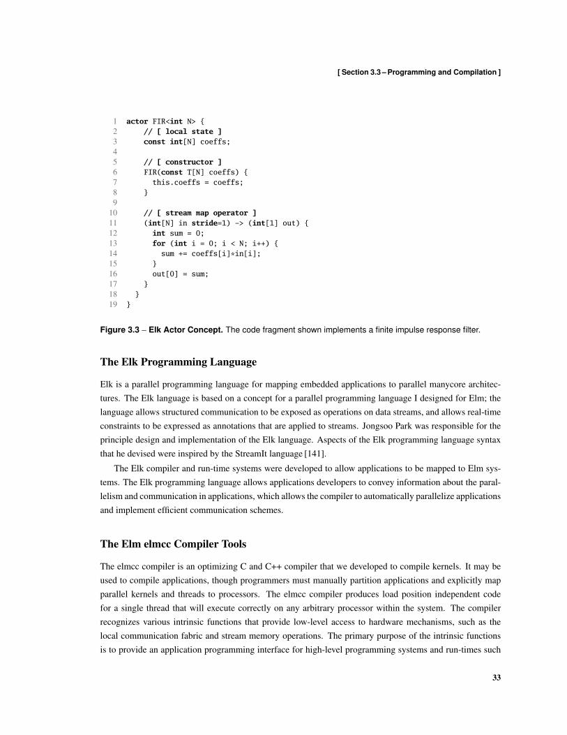
[ Section 3.3 – Programming and Compilation ]
1 actor FIR<int N> {2 // [ local state ]3 const int[N] coeffs;45 // [ constructor ]6 FIR(const T[N] coeffs) {7 this.coeffs = coeffs;8 }9
10 // [ stream map operator ]11 (int[N] in stride=1) -> (int[1] out) {12 int sum = 0;13 for (int i = 0; i < N; i++) {14 sum += coeffs[i]*in[i];15 }16 out[0] = sum;17 }18 }19 }
Figure 3.3 – Elk Actor Concept. The code fragment shown implements a finite impulse response filter.
The Elk Programming Language
Elk is a parallel programming language for mapping embedded applications to parallel manycore architec-tures. The Elk language is based on a concept for a parallel programming language I designed for Elm; thelanguage allows structured communication to be exposed as operations on data streams, and allows real-timeconstraints to be expressed as annotations that are applied to streams. Jongsoo Park was responsible for theprinciple design and implementation of the Elk language. Aspects of the Elk programming language syntaxthat he devised were inspired by the StreamIt language [141].
The Elk compiler and run-time systems were developed to allow applications to be mapped to Elm sys-tems. The Elk programming language allows applications developers to convey information about the paral-lelism and communication in applications, which allows the compiler to automatically parallelize applicationsand implement efficient communication schemes.
The Elm elmcc Compiler Tools
The elmcc compiler is an optimizing C and C++ compiler that we developed to compile kernels. It may beused to compile applications, though programmers must manually partition applications and explicitly mapparallel kernels and threads to processors. The elmcc compiler produces load position independent codefor a single thread that will execute correctly on any arbitrary processor within the system. The compilerrecognizes various intrinsic functions that provide low-level access to hardware mechanisms, such as thelocal communication fabric and stream memory operations. The primary purpose of the intrinsic functionsis to provide an application programming interface for high-level programming systems and run-times such
33
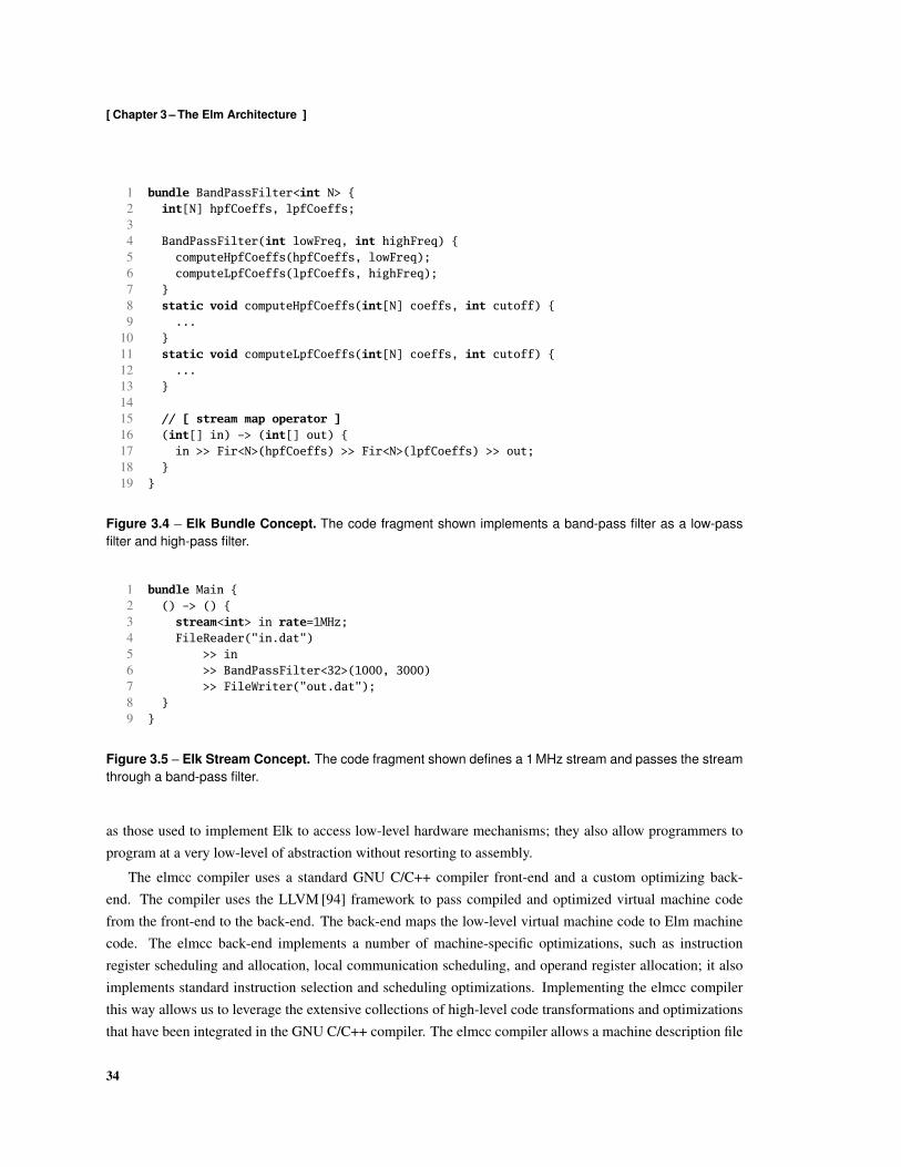
[ Chapter 3 – The Elm Architecture ]
1 bundle BandPassFilter<int N> {2 int[N] hpfCoeffs, lpfCoeffs;34 BandPassFilter(int lowFreq, int highFreq) {5 computeHpfCoeffs(hpfCoeffs, lowFreq);6 computeLpfCoeffs(lpfCoeffs, highFreq);7 }8 static void computeHpfCoeffs(int[N] coeffs, int cutoff) {9 ...
10 }11 static void computeLpfCoeffs(int[N] coeffs, int cutoff) {12 ...13 }1415 // [ stream map operator ]16 (int[] in) -> (int[] out) {17 in >> Fir<N>(hpfCoeffs) >> Fir<N>(lpfCoeffs) >> out;18 }19 }
Figure 3.4 – Elk Bundle Concept. The code fragment shown implements a band-pass filter as a low-passfilter and high-pass filter.
1 bundle Main {2 () -> () {3 stream<int> in rate=1MHz;4 FileReader("in.dat")5 >> in6 >> BandPassFilter<32>(1000, 3000)7 >> FileWriter("out.dat");8 }9 }
Figure 3.5 – Elk Stream Concept. The code fragment shown defines a 1 MHz stream and passes the streamthrough a band-pass filter.
as those used to implement Elk to access low-level hardware mechanisms; they also allow programmers toprogram at a very low-level of abstraction without resorting to assembly.
The elmcc compiler uses a standard GNU C/C++ compiler front-end and a custom optimizing back-end. The compiler uses the LLVM [94] framework to pass compiled and optimized virtual machine codefrom the front-end to the back-end. The back-end maps the low-level virtual machine code to Elm machinecode. The elmcc back-end implements a number of machine-specific optimizations, such as instructionregister scheduling and allocation, local communication scheduling, and operand register allocation; it alsoimplements standard instruction selection and scheduling optimizations. Implementing the elmcc compilerthis way allows us to leverage the extensive collections of high-level code transformations and optimizationsthat have been integrated in the GNU C/C++ compiler. The elmcc compiler allows a machine description file
34

[ Section 3.3 – Programming and Compilation ]
1 actor CombineDft<int N> {2 complex_f[N/2] w; // coefficients3 CombineDft() {4 for (int i = 0; i < N/2; i++) {5 w[i] = complex_f(cos(-2*PI*i/N), sin(-2*PI*i/N));6 } }78 (complex_f[N] in) -> (complex_f[N] out) {9 for (int i = 0; i < N/2; i++) {
10 complex_f y0 = in[i];11 complex_f y1 = in[N/2 + i];12 complex_f y1w = y1*w[i];13 out[i] = y0 + y1w;14 out[N/2 + i] = y0 - y1w;15 } } }1617 actor FftReorderSimple<int N> {18 (complex_f[N] in) -> (complex_f[N] out) {19 for (int i = 0; i < N; i+=2) {20 out[i/2] = in[i];21 }22 for (int i = 1; i < N; i+=2) {23 out[N/2 + i/2] = in[i];24 } } }2526 bundle FftReorder<int N> {27 (complex_f[] in) -> (complex_f[] out) {28 stream<complex_f>[log2(N)] temp;29 in >> temp[0];30 for (int i = 1; i < (N/2); i*=2) {31 temp[log2(i)] >> FftReorderSimple<N/i>() >> temp[log2(i) + 1];32 }33 temp[log2(N) - 1] >> out;34 } }3536 bundle Main {37 () -> () {38 int N = 256;39 stream<complex_f>[log2(N) + 1] temp;40 FileReader("in.dat") >> FftReorder<N>() >> temp[0];41 for (int i = 2; i <= N; i *= 2) {42 temp[log2(i) - 1] >> CombineDft<i>() >> temp[log2(i)];43 }44 temp[log2(N)] >> FileWriter("out.dat", 3072);45 } }
Figure 3.6 – Elk Implementation of FFT.
35
[ Chapter 3 – The Elm Architecture ]
to be passed as a command line argument. Machine description files describe the capabilities and resourcesof the target machine, and are typically used to conduct sensitivity experiments in which machine resourcessuch as the number of operand registers are varied.
The elmcc linker allows multiple object files produced by the elmcc compiler to be combined into Ensem-ble and application bundles. The linker resolves and binds those symbols and locations that can be resolvedat link time, such as the locations of data and code objects in the system and Ensemble address spaces. Likethe elmcc compiler, the linker allows a machine description file to be passed as a command line argument.
The elmcc loader is responsible for binding any remaining unresolved symbols when applications load.The loader requires both an application bundle and an application mapping file. The application bundlecontains the application code and data objects, and may contain symbolic references to Ensembles, distributedmemories, processors, and so forth. The application mapping file specifies where code and data objects shouldbe placed when an application is loaded, and is used to resolve symbolic address and location references. Themodified application bundle produced by the loader may contain a combination of load position independentcode, which will execute correctly on any processor within a system; load position dependent code, whichonly executes correctly on a specific processor; and relative load position dependent code, which will executecorrectly provided that other code objects are mapped similarly. Relative load position code typically containsreferences that access the local communication fabric or local Ensemble memory. The loader requires amachine description file that specifies the Ensemble and memory resources of a machine.
3.4 Chapter Summary
This chapter described an Elm system and introduced many of the concepts and ideas that will be developedin subsequent chapters. A common theme throughout the thesis will be ways in which we can improveefficiency by exposing distributed computation, communication, and storage resources to software. Thisallows software to exploit parallelism and locality in applications.
The following five chapters extend the concepts introduced in this chapter and describe the Elm architec-ture in greater detail. The chapters follow a common organization structure a common structure. We presentthe major concepts presented in the chapter. We describe the application of these concepts to Elm, usingspecific mechanisms in the Elm architecture to provide concrete examples of how general concepts, and thenpresent examples that illustrate how the ideas presented in architecture section improve efficiency. We thenpresent a quantitative evaluation of the concepts and architectural mechanisms presented in the chapter. Theevaluation is followed by a summary of related work.
36
Chapter 4
Instruction Registers
This chapter introduces instruction registers, distributed collections of software-managed registers that extendthe memory hierarchy used to deliver instructions to function units. Instruction registers exploit instructionreuse and locality to improve efficiency. They allow critical instruction working sets such as loops andkernels to be stored close to function units. Instruction registers are implemented efficiently as distributedcollections of small instruction register files. Distributing the register files allows instructions to be storedclose to function units, reducing the energy consumed transferring instructions to data-path control points.The aggregate instruction storage capacity provided by the distributed collection of register files allows themto captured important working sets, while the small individual register files are fast and inexpensive to access.
The remainder of this chapter is organized as follows. I explain general concepts and describe the opera-tion of instruction registers. I then describe microarchitectural details of the instruction register organizationimplemented in Elm. This is followed by examples illustrating the use of instruction registers. I then de-scribe compiler algorithms for allocating and scheduling instruction registers. I conclude this chapter with acomparison of the performance and efficiency of instruction registers to similar mechanisms for reducing theamount of energy expended delivering instructions.
4.1 Concepts
Embedded applications are dominated by kernels and loops that have small instruction working sets andextensive instruction reuse and locality. Consequently, a significant fraction of the instruction bandwidthdemand in embedded applications can be delivered from relatively small memories.
The instruction caches and software-managed instruction memories found in most embedded processorshave enough capacity to accommodate working sets that are larger than most embedded kernels. Often,first-level instruction caches are made as large as possible while still allowing the cache to be accessed in asingle cycle at the desired clock frequency. Consequently, the instruction caches found in common embeddedprocessors are much larger than a single kernel or loop body: it is not uncommon to find embedded processorswith instruction caches ranging from 4 KB to 32 KB, while many of the important kernels and loops in
37

[ Chapter 4 – Instruction Registers ]
InstructionRegister File
(IRF)
InstructionRegister File
(IRF)IP
Backing Memory
instruction register namespaceglobal address namespace
issued instruction issued instruction
Figure 4.1 – Instruction Register Organization. Instruction registers are software-managed memory that letsoftware capture critical instruction working sets close to the function units. The instruction registers form theirown namespace, which differs from the address space used to identify instructions in the backing memory.Instruction registers are implemented as small, fast register files. The instruction register files are distributedto reduce the energy expended transferring instructions from the register files to the function units. Softwareorchestrates the movement of instructions from the backing memory to the instruction registers. The instructionpointer (IP) specifies the address of the next instruction to be issued from the instruction registers.
embedded applications comprise fewer than 1000 instructions and are smaller than 4 KB. Increasing the cachecapacity reduces the number of instructions that must be fetched from the memories that back the instructioncache, which improves performance and often improves efficiency as well. It improves performance byreducing the number of stalls that occur when there is a miss in the instruction cache; it improves efficiencyby reducing the amount of energy spent transferring instructions from backing memories, which are typicallymuch more expensive to access. However, the energy expended accessing the first-level instruction cacheincreases with its capacity. In this way larger instruction caches reduce the average energy expended accessinginstructions across large instruction working sets at the expense of increasing the energy expended accessinginstructions within small working sets, such as a loop nest or kernel.
Elm reduces the cost of delivering instructions by extending the instruction storage hierarchy with adistributed collection of software-managed instruction register files (IRFs) to capture the small instructionworking sets found in loops and kernels. The organization is illustrated in Figure 4.1. Essentially, we canreason about instruction registers as collections of very small software-managed caches residing at the bottomof the instruction memory hierarchy. We use the term register because, like their data register equivalents,instruction registers define a unique architectural namespace. Furthermore, instruction registers are explicitlymanaged by software, which is responsible for allocating instruction registers and scheduling load operationsto transfer instructions into registers.
Unlike caches, instruction registers do not use tags to determine which instructions are resident. Issuing
38
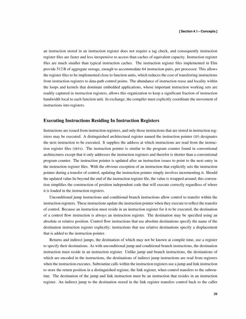
[ Section 4.1 – Concepts ]
an instruction stored in an instruction register does not require a tag check, and consequently instructionregister files are faster and less inexpensive to access than caches of equivalent capacity. Instruction registerfiles are much smaller than typical instruction caches. The instruction register files implemented in Elmprovide 512 B of aggregate storage, enough to accommodate 64 instruction pairs, per processor. This allowsthe register files to be implemented close to function units, which reduces the cost of transferring instructionsfrom instruction registers to data-path control points. The abundance of instruction reuse and locality withinthe loops and kernels that dominate embedded applications, whose important instruction working sets arereadily captured in instruction registers, allows this organization to keep a significant fraction of instructionbandwidth local to each function unit. In exchange, the compiler must explicitly coordinate the movement ofinstructions into registers.
Executing Instructions Residing In Instruction Registers
Instructions are issued from instruction registers, and only those instructions that are stored in instruction reg-isters may be executed. A distinguished architectural register named the instruction pointer (IP) designatesthe next instruction to be executed. It supplies the address at which instructions are read from the instruc-tion register files (IRFs). The instruction pointer is similar to the program counter found in conventionalarchitectures except that it only addresses the instruction registers and therefor is shorter than a conventionalprogram counter. The instruction pointer is updated after an instruction issues to point to the next entry inthe instruction register files. With the obvious exception of an instruction that explicitly sets the instructionpointer during a transfer of control, updating the instruction pointer simply involves incrementing it. Shouldthe updated value lie beyond the end of the instruction register file, the value is wrapped around; this conven-tion simplifies the construction of position independent code that will execute correctly regardless of whereit is loaded in the instruction registers.
Unconditional jump instructions and conditional branch instructions allow control to transfer within theinstruction registers. These instructions update the instruction pointer when they execute to reflect the transferof control. Because an instruction must reside in an instruction register for it to be executed, the destinationof a control flow instruction is always an instruction register. The destination may be specified using anabsolute or relative position. Control flow instructions that use absolute destinations specify the name of thedestination instruction register explicitly; instructions that use relative destinations specify a displacementthat is added to the instruction pointer.
Returns and indirect jumps, the destination of which may not be known at compile time, use a registerto specify their destinations. As with unconditional jump and conditional branch instructions, the destinationinstruction must reside in an instruction register. Unlike jump and branch instructions, the destinations ofwhich are encoded in the instructions, the destinations of indirect jump instructions are read from registerswhen the instruction executes. Subroutine calls within the instruction registers use a jump and link instructionto store the return position in a distinguished register, the link register, when control transfers to the subrou-tine. The destination of the jump and link instruction must be an instruction that resides in an instructionregister. An indirect jump to the destination stored in the link register transfers control back to the caller
39

[ Chapter 4 – Instruction Registers ]
when the subroutine completes.
Loading Instructions into Instruction Registers
Software explicitly coordinates the movement of instructions into instruction registers by executing instruc-tion loads. An instruction load transfers a contiguous block of instructions from memory into a contiguousset of registers. Software specifies the size of the instruction block, where the block is to be loaded in theinstruction register file, and where the block resides in memory. The size of the instruction block determinesthe number of instructions that are transferred when the load executes. The processor can continue to ex-ecute instructions while instructions load provided that control does not transfer to an instruction registerwith a load pending. Should control transfer to a register with a load pending, the processor stalls until theinstruction arrives from the backing memory.
Instruction registers provide an effective mechanism for decoupling the fetching of instructions frommemory and the issuing of instructions to the function units. This decoupling lets software hide memoryaccess latencies. Software anticipates transfers of control, and proactively initiates instruction loads to fetchany instructions that are not present in the instruction registers.
Instruction loads may specify absolute or relative destinations. Loads that specify absolute destinationsencode the name of the instruction register at which the block is to be loaded. Loads that specify relative des-tinations encode a displacement that is added to the instruction pointer to determine the destination. Allowinginstruction loads to specify relative destinations simplifies the generation of position independent code thatwill execute correctly regardless of where it is loaded in the instruction registers.
Instruction loads may specify the memory address at which the instruction block reside directly or in-directly. Loads that specify the address directly encode the effective address of the instruction block in theinstruction word. Loads that specify the address indirectly encode a register name and displacement in theinstruction word; the effective address is determined when the load executes by adding the displacement tothe contents of the specified register. The direct addressing mode is used when the location of the instructionblock is known at compile time. This commonly occurs when an instruction block is transferred to a localsoftware-managed memory before being loaded into instruction registers. The indirect addressing mode isused when the address of the instruction block cannot be determined at compile time. The indirect addressingmode is also used when the address of the instruction block is too large to be encoded directly. Additionally,the indirect addressing mode can be used to implement register indirect jumps by executing an instructionload followed by a jump. The instruction load uses the register that contains the address of the indirect jumptarget to load the target instruction; the jump transfers control to the target instruction after it has been loaded.
Contrasting Instruction Registers and Caches
Instead of instruction registers, we might consider using small instruction caches in the first level of the in-struction memory hierarchy. These small caches are commonly referred to as filter caches. Like instructionregisters, filter caches allow small instruction working sets to be captured close to the function units in mem-ory that is less expensive to access than the first-level instruction caches typically used in most processors.
40
[ Section 4.1 – Concepts ]
Perhaps the most obvious difference between instruction registers and filter caches is the use of tags to dy-namically determine which instructions are present in a cache. More fundamentally, instruction registers andfilter caches differ in the separation of management policy and responsibilities between software and hard-ware: instruction registers let software decide which instructions are displaced when instructions are loaded,which instructions are loaded together, and when instructions are loaded.
Naming
To request an instruction stored in a cache, a processor sends the complete address of the desired instructionto the cache. Some of the address bits are used to identify the set in which the block containing the desiredinstruction will reside if the instruction is present in the cache. Most of the address bits are used to checkthe block tag to determine whether the desired instruction is present, and most often the instruction is presentin the cache. When the instruction is not present, the cache uses the address to determine the address ofthe cache block that needs to be requested from the backing memory. Because the entire address of thedesired instruction is always needed to access the cache, the program counter must be wide enough to store acomplete memory address.
To request an instruction stored in an instruction register, the processor sends a short instruction registeridentifier to the instruction register file. As described previously, the instruction pointer stores the identifierof the next instruction to be executed. Because there are relatively few instruction registers, the instructionpointer is short and less expensive to maintain than a program counter. The processor only needs to send amemory address to the instruction register file when loading instructions, an infrequent operation.
Placement and Replacement
The placement or mapping policy of a cache determines where a block may be placed within the cache.Consequently, it also affects, and may completely determine, which block is displaced when a block is loadedinto the cache. Caches typically implement a fixed placement policy, though machines let software influencethe placement policy. For example, some allow software to configure the set associativity of a cache [55].When considering how the placement policy affects the cost of accessing an instruction cache, we need toconsider the cost of accessing an instruction from the cache when the instruction is present in the cache, thecost of accessing an instruction when the instruction is not present in the cache and must be loaded fromthe backing memory, and the rate at which instructions are loaded from the backing memory. The cost ofaccessing an instruction that is not present in the cache is dominated by the cost of accessing the backingmemory rather than storing the instruction in the cache.
Direct mapped caches allow a block to appear in only one place. Because only one entry is searched whena direct mapped cache is accessed, direct mapped caches usually store block tags in SRAM that is accessed inparallel with the instruction array. Set associative caches allow a block to appear in a restricted set of places.Accessing a set associative cache can consume more energy than accessing a direct mapped cache of the samecapacity, as multiple ways may need to be searched, but the improvement in the cache hit rate can reducethe number of accesses to the backing memory enough to provide an overall reduction in the average access
41
[ Chapter 4 – Instruction Registers ]
energy. Set associative caches may store block tags in SRAM and access multiple tags in parallel. Highlyassociative caches with many parallel ways typically store the block tags in content addressable memories toallow all of the tags to be checked in parallel [105]. The match line can be used to drive the word-line of theinstruction array so that the instruction array is only accessed when there is a hit. Fully associative cachesallow a block to appear anywhere in the cache. Though impractical for large caches, filter caches are oftensmall enough and require few enough tags to be fully associative.
Like fully associative caches, an instruction may be placed at any location in an instruction register file.Because software controls where an instruction load places instructions, software decides which instructionsare replaced when new instructions are loaded. The elmcc compiler is often able to achieve effective hit ratesthat are competitive with or better than a cache by statically analyzing code to determine which instructionsare best candidates for replacement. This is possible because a compiler can infer which instructions arelikely to be executed in the future from the structure of code.
Similar optimization can be performed for a direct mapped cache when the compiler can determine wheninstructions will conflict in the cache. The code layout determines which instructions will conflict in thecache, and therefore the code layout phase must place instructions to avoid conflicts. Compilers may find itdifficult to perform these types of code placement optimizations across function call boundaries. The addressof a function provides both the name used by callers to identify the function and determines where it willreside in an instruction cache. To avoid conflicts between a function and its callers, the compiler must placethe function such that it does not conflict with the locations at which it is called. This requires that a compilerconsider both the function and its callers when placing instructions to avoid conflicts, which is similar instructure to register allocation. Instruction registers allow the caller to decide where the function will beloaded, and therefore allows the caller to decide which instructions are displaced. This greatly simplifies theproblem of laying out code to avoiding conflicts, as it reduces it to a local problem of deciding where to loadinstructions in the instruction register rather than a global problem of deciding how to structure an applicationto reduce conflicts.
Because the number of instruction registers is expected to be small, it will often not be possible for afunction and its caller to reside in the instruction registers without it being productive to inline the function.Instruction registers allow functions to be inlined without replicating the inlined function body at every callsite. Instead, a single instance of the function can be loaded into the instruction registers at the inlined calllocations. This avoids the problem of code expansion when function calls are inlined.
When a function is too large to be productively inlined and the compiler is able to bound the function’sinstruction register requirements, the compiler can allocate instruction registers to the called function andhave the calling function restore the instruction registers when control returns. This convention is useful forleaf function calls. Because a leaf function does not call other functions, the compiler can easily bound itsinstruction register requirements.
42

[ Section 4.1 – Concepts ]
aes conv2d crc crosscor dct !r hu"man jpeg rgb2yuv viterbi
1.0
0.0
1.0
0.0
miss rate [normalized]
instructions transferred from backing memory [normalized]
block size = 2 instruction pairs block size =4 instruction pairs block size = 8 instruction pairs
Figure 4.2 – Impact of Cache Block Size on Miss Rate and Instructions Transferred. The instructionstransferred and miss rate are for a direct-mapped cache with a capacity of 64 instruction-pairs. The upperplot shows the relative number of instructions that are transferred from the backing memory; the lower plotshows the relative miss rate. The data in both plots are normalized within each kernel. The average numberof instructions that are loaded from the backing memory increases with the block size, while the miss ratedecreases. The abrupt increase in the dct kernel data results from conflict misses that occur when the blocksize is 8 instruction-pairs. The alignment of instructions within the kernel causes conflicts between instructionsat the start and end of the loop. Consequently, there are 2 conflict misses per iteration of the loop despite thecache having enough capacity to accommodate the loop.
Block Size
The block size selected for a cache affects the number of tags that must be provisioned. It also affects thenumber of instructions that are loaded from the backing memory when there is a cache miss. Larger blocksbetter exploit any spatial instruction locality that is present in an application, and increasing the block sizecan reduce the miss rate when executing instruction sequences that exhibit significant spatial locality. Thereduction in the miss rate improves performance, but does not reduce the number of instructions that areloaded from the backing store. Increasing the block size may increase the number of instructions that areloaded from the backing store. This occurs when the larger block size increases the number of instructionsthat are transferred to the cache but not executed before the block is replaced, as is illustrated by the datapresented in Figure 4.2.
For a fixed cache capacity, increasing the block size reduces the number of tags, as each tag covers moreinstructions. Because the cost of searching the tags increases with the number of tags, increasing the block
43

[ Chapter 4 – Instruction Registers ]
size reduces the contribution of the tag search to the instruction access energy. However, increasing the blocksize can result in additional conflict misses. Because filter caches are small, and therefore hold relativelyfew blocks, the increase in the number of conflict misses caused when the block size is increased can besignificant, as illustrated by the miss rate observed for the dct kernel in Figure 4.2.
Software-defined instruction blocks provide a flexible mechanism for specifying and encoding locality.The instructions in a block exhibit significant spatial and temporal locality, and typically exhibit significantreuse. Because software determines the size of the instruction block that is loaded by each instruction loadoperation, software can avoid inadvertently loading instructions that may not be executed when control entersthe block. However, additional instructions must be executed to initiate the loading of instructions intoinstruction registers, which expands code sizes and partially neutralizes some of the reduction.
4.2 Microarchitecture
This section describes the instruction register architecture implemented in the Elm prototype and discussesdesign considerations that influenced the microarchitecture. Figure 4.3 illustrates in detail the microarchitec-ture of the instruction load (IL) and instruction fetch (IF) stages of the pipeline. Instructions are issued inpairs from the instruction register files, each of which has 64 registers. The instruction register files are two-port memories, with a dedicated read port and a dedicated write port. This allows the loading of instructionsto overlap with the execution of instructions from the instruction registers.
The instruction register management unit (IRMU) coordinates the movement of instructions from thebacking memory to the instruction registers. Instruction load commands are sent to IRMU from the XMUpipeline. The IRMU is decoupled from the function unit pipelines, which allows the processor to continueexecuting instructions while instructions are being loaded. The IRMU implemented Elm can handle a singleinstruction load at a time. Attempts to initiate a load operation while one is outstanding causes the pipelineto stall.
The instruction load unit implements the address generators and control logic that coordinates the transferof instructions from the backing memory to the instruction registers. The instruction load unit has two ad-dress generators: one for generating memory addresses, and one for generating instruction register addresses.When an instruction block is loaded from a remote memory, and therefore must traverse the on-chip intercon-nection network, the memory address generator is only used to compute the address of the instruction block,and not the instructions within the block. The block address and the block size are sent to the local networkinterface, which performs a single block memory transfers to fetch the entire instruction block. This reducesthe number of addresses that must be generated locally, and more importantly reduces the number of memoryoperations that traverse the network.
The IRMU uses a pending load (PL) scoreboard to track which instruction registers are waiting for in-structions to arrive from the backing memory. When an instruction load is initiated, the IRMU updates the PLscoreboard to indicate that the destination registers are invalid. The scoreboard is updated when instructionsarrive from the backing memory to indicate that the destination registers now contain the expected instruc-tions. When the IRMU is loading instructions, the PL scoreboard is used to determine whether the requested
44

[ Section 4.2 – Microarchitecture ]
InstructionRegister File
(IRF)
InstructionRegister File
(IRF)
branch target
Load Unit
Translate Unit
XMU ALU
IRMU
IP
+1
PL scoreboard
load command
xmu instruction alu instruction
Backing Memory
instruction pair
address
issue stall
!"
#$
BUPipeline ControlLogic
"%
&'
instruction register namespaceglobal address namespace
#(
Figure 4.3 – Instruction Register Microarchitecture. The instruction register management unit (IRMU)coordinates the movement of instructions from the backing memory to the instruction registers. The IRMUuses a pending load (PL) scoreboard to track which instruction registers are waiting for instructions to arrivefrom the backing memory
instructions are available for issue. The same instruction pointer value is sent to the scoreboard and instruc-tion registers, and the scoreboard and instruction registers are accessed in parallel. The scoreboard behaveslike full-empty bits on the instruction register values, except that the scoreboard is only accessed when theIRMU is loading instructions so that energy is not expended accessing the scoreboard when the IRMU is idle.
The PL scoreboard in Elm is implemented as a vector of 64 registers, one per instruction register address.This allows the IRMU to track each instruction register pair independently, which is feasible because thenumber of instruction registers is small. Though the energy expended maintaining the scoreboard contributesto the cost of loading instructions, a more important design consideration is the impact of the scoreboardon the cycle time, particularly when designs use deeper instruction register files. The energy expendedmaintaining the scoreboard is a less significant concern because the scoreboard is only active when the IRMU
45

[ Chapter 4 – Instruction Registers ]
is loading instructions, which tends to be infrequent.
The size of the scoreboard can be reduced if it tracks contiguous sets of instruction registers rather thanindividual entries. Increasing the size of the sets that the scoreboard tracks will reduce its size, but the loss ofresolution can cause the processor to stall unnecessarily during instruction loads. In the limit of a single blockthat covers all of the instruction registers, one bit could be used to track all of the registers. Such a simplescoreboard would be inexpensive to maintain and would offer fast access times, but the processor would beforced to stall during every instruction load until every instruction in the instruction block arrives from thebacking memory. If such a scoreboard where used, the instruction register files could be implemented assingle-port memories, as it would not be necessary to concurrently read one instruction register while writinga different register. Performance would suffer, but the instruction registers would be less expensive to access.Such a design would be appropriate when instruction reuse within the significant kernels of an applicationallows most instructions to be statically placed within the instruction registers.
Control flow instructions execute in the branch unit (BU), which is implemented in the decode stageand contains a dedicated link register. Conditional branch instructions are implemented as predicated jumpinstructions, with dedicated predicate registers used to control whether a branch is taken. When a jump andlink instruction executes, the branch unit stores the return instruction pointer to the link register. The linkregister also provides the destination for a jump register instruction when it executes. The dedicated linkregister allows the branch unit to write the link register when a jump and link instruction is in the decodestage, before the instruction reaches the write-back stage, simplifying the bypass network. It also lets thebranch unit read the operand to a jump register instruction before the instruction reaches the register files,reducing the delay associated with forwarding the destination to the instruction register files. When thedesired destination of an indirect jump is not in the link register, the destination must be explicitly movedto the link register. In effect, the move instruction that updates the predicate register behaves like a prepare-to-branch instruction [48], explicitly informing the hardware of the intended branch destination. The valuestored in the link register can be saved by moving it to a different register or storing it to memory.
The destinations of relative jump and branch instructions are resolved in the translation unit as they areloaded from the backing memory. Consequently, all control flow destinations are stored as absolute desti-nations within the instruction registers, which simplifies the branch unit because it does not need an addressgenerator. Most processors resolve relative destinations when control flow instructions execute. Because aninstruction is typically executed more than once after it is loaded, resolving the destination when instructionsload reduces activity within the hardware that computes the destination address, thereby reducing the energyexpended delivering instructions to the processor.
In addition to conditional branch control flow instructions, the branch unit also executes loop instructions.Loop instructions use predicate registers to control whether the loop transfers control. A subset of the pred-icate registers provide counters that can be used to control the execution of loops. The predicate field of anextended predicate register is set when the counter value is zero. When a loop instructions uses one of theseextended predicate registers, the branch unit decrements the counter stored in the predicate register in thedecode stage. Typically this reduces loop overheads by eliminating the bookkeeping instructions that updateloop induction variables after each iteration of a loop. Updating the register that controls whether the branch
46

[ Section 4.3 – Examples ]
is taken early in the pipeline reduces the minimum number of instructions that must appear in a loop body toprevent dependencies on the predicate register from stalling the pipeline, which allows Elm to execute shortloops efficiently. Software techniques for reducing the number of branch and overhead instructions such asloop unrolling, which replicates multiple copies of a loop body, provide similar benefits at the expense of ex-panded code sizes. Loop unrolling optimizations can be counterproductive with instruction registers becausethe increase in code size may prevent the instruction registers from accommodating important instructionworking sets.
4.3 Examples
This section provides several examples that illustrate the use of instruction registers. To simplify the exam-ples, the assembly listings that appear in this section show only those instructions that execute in the XMUfunction unit. To further simplify the examples, the delay slots and most of the instructions that do not affectthe transfer of control and do not affect the management of the instruction registers are elided; those instruc-tions that do not affect the transfer of control and instruction registers that are shown simplify serve as placemarkers in the code.
Loading and Executing Instructions
The assembly code fragment shown in Figure 4.4 provides a useful example for illustrating several basicconcepts associated with the use of instruction registers to capture important instruction working sets. Theassembly code as shown lacks instructions for loading instructions into instruction registers, which wouldbe introduced during the instruction register allocation and scheduling compiler pass. The size of each basicblock is annotated in the control-flow graph that appears in Figure 4.4. As illustrated by the control-flowgraph, the code contains three basic blocks and one loop.
Before passing the code in Figure 4.4 to the assembler, the instruction register allocation phase of thecompiler must allocate instruction registers and schedule instruction loads. Instruction register allocationand load scheduling are important phases in the compilation process. The allocation of instructions to regis-ters affects efficiency by exposing or limiting opportunities for instruction reuse within different instructionworking sets. The scheduling of instruction loads also affects performance. By anticipating transfers of con-trol to instructions that are not in registers and initiating instruction loads before instructions are needed, thecompiler can hide the latency associated with loading instructions into registers.
A simple though typically rather inefficient strategy for allocating and scheduling instruction registers is toload each basic block immediately before control transfers to it. This is readily accomplished by introducingjump-and-load instructions at the outgoing edges of each basic block in the control-flow graph. The resultingcode can be improved using a simple optimization that removes load operations that are clearly redundant.An example of a trivially redundant load operations is one that load the instruction block in which it appears.In effect, this simple strategy implements an allocation policy that assigns all of the instruction registers toeach basic block and a scheduling policy that defers instruction loads as late as possible.
47

[ Chapter 4 – Instruction Registers ]
BB1
BB2
BB3
BB1:
BB2:
BB3:loop.clear pr0 [@BB2] (4)mov r2 #4
mov r1 #3
mov r1 #1
mov r1 #2
mov r1 #5
......
...
100
109110
129130
139
[10]
[20]
[10]
assembly code fragment control-!ow graph
Figure 4.4 – Assembly Code Fragment of a Loop that can be Captured in Instruction Registers. The sim-plified assembly code contains a single loop of 20 instruction pairs, as the loop instruction at line 129 transferscontrol to the instruction pairs at line 110. Instructions that do not affect control flow have been replaced withunique mov instructions. Assembly statements at the boundaries of basic blocks are numbered in the codefragment, and the illustration of the corresponding control-flow graph shows the number of instructions in eachbasic block.
Figure 4.5 shows the assembly code fragment produced by the simple allocation and scheduling strategyafter the redundant load elimination optimization is performed. Each jump-and-load instruction loads a newinstruction block when control transfers between different basic blocks. The instruction blocks are illustratedat the right of the assembly code; the assembly statements that declare and define the instruction blocks arenot shown to avoid cluttering the assembly code. For comparison, the basic block structure of the originalcode is illustrated at the left of the assembly code. There is a precise correspondence between the basic blocksin the original assembly code and the instruction blocks, as each instruction block encompasses a single basicblock. The assembler allows assembly statements to use @ expressions to specify the address of labels inthe assembly code. The assembler also allows statements to use # expressions to refer to the length of aninstruction block. For example, the jump-and-load instruction at line 100, which loads instruction block IB1,specifies that the instruction block resides at the memory address that the expression @IB1 resolves to, andthat the length of the instruction block is the size that #IB1 resolves to.
Because the placement of the jump-and-load instructions in Figure 4.5 ensure that only one instructionblock needs to be present in the instruction registers at any point in the execution of the code fragment, allof the jump-and-load instructions in Figure 4.5 use ir0 as their targets. Consequently, each instruction loaddisplaces instructions in the current basic block loaded instructions, and an instruction load operation may
48

[ Section 4.3 – Examples ]
BB1:
BB2:
BB3:
loop.clear pr0 [@BB2] (4)
mov r2 #4
mov r1 #3
mov r1 #1
mov r1 #2
mov r1 #5
......
...
100
110111
131132
142
jld [ir0] [@IB3] (#IB3)133
jld [ir0] [@IB2] (#IB2)112
jld [ir0] ...
IB1
IB2
IB3
IB1
IB2
IB3
IB1
BB2
BB2
BB2
BB2
BB2
IB2
IB3
load execute
BB0
143
jld [ir0] [@IB1] (#IB1)101
assembly code fragment execution schedule
[11]
[21]
[11]
time
Figure 4.5 – Assembly Code Produced with a Simple Allocation and Scheduling Strategy. The corre-sponding instruction load and execution schedule is shown to the right of the assembly code.
displace the jump-and-load that initiated the operation. For example, the jump-and-load instruction at line112 issues from instruction register ir10 and loads instruction block IB2 into ir0 through ir20.
The simple allocation and scheduling strategy is able to exploit what instruction reuse exists within theexample. The loop involving basic block BB2 provides the only opportunity for instruction reuse, and theredundant load optimization ensures that the simple allocation and scheduling strategy loads the loop bodyonly once.
However, the processor always stalls when a jump-and-load instruction executes because it must wait forthe instruction register management unit to load the instruction that control transfers to. As illustrated in theexecution schedule of Figure 4.5, using jump-and-load instructions to load each basic block individually andimmediately before control transfers to it causes the processor to stall whenever control transfers to a differentbasic block. For example, execution stalls when control transfers from basic block BB1 to basic block BB2,and again when control transfers from BB2 to basic block BB3.
The compiler can eliminate some of the stalls in the execution schedule of Figure 4.5 by scheduling someinstruction loads earlier, as illustrated in Figure 4.6. In the code shown in Figure 4.6, the jump-and-loadinstruction at line 100 loads basic blocks BB1, BB2, and BB3 as control transfers to basic block BB1. Figure 4.6shows the resulting execution schedule. In addition to eliminating stalls, loading multiple basic blocks as asingle instruction block reduces the number of instructions inserted by the compiler to manage the instructionregisters. The code fragment in Figure 4.6 contains two fewer XMU instructions, which may improve theexecution time and reduce the number of instructions that are transferred from the backing memory when the
49
[ Chapter 4 – Instruction Registers ]
BB1:
BB2:
BB3:loop.clear pr0 [@BB2] (4)mov r2 #4
mov r1 #3
mov r1 #1
mov r1 #2
mov r1 #5
......
...
101
110
130
140
131
111
jld [ir0] ...
IB1
BB1 BB1
BB2
BB2
BB2
BB2
BB2
BB2
BB3
BB0
141
100 jld [ir0] [@IB1] (#IB1)
BB2
BB3
load execute
execution schedule
time
[41]
assembly code fragment
Figure 4.6 – Assembly Code Fragment Produced when Instruction Load is Advanced. The assemblycode fragment shows the loop when the instruction load operations that load the individual basic blocks arescheduled before control enters the region. The load operations are merged into the single jump-and-loadoperation at line 100.
fragment is loaded into instruction registers.
Executing a Loop that Exceeds the Capacity of the Instruction Registers
The assembly code fragment shown in Figure 4.7 is similar in structure to the fragment used in the previousexample. However, it differs in that the loop body exceeds the capacity of the instruction registers. The sizeof each basic block appears in the control-flow graph illustrated in Figure 4.7. As in the previous example,the code fragment has three basic blocks and one loop.
As before, the compiler must allocate instruction registers and schedule instruction loads before passingthe code shown in Figure 4.7 to the assembler. Because the code fragment contains a basic block that exceedsthe capacity of the instruction registers, the simple instruction register allocation and scheduling strategy usedin the previous example cannot be applied.
Before proceeding to explain how the compiler should allocate and schedule instruction registers in thisexample, we should be aware that in some cases the compiler may be able to apply high-level code trans-formations such as loop fission to split large loops into multiple smaller loops, each of which will comprisefew enough instructions to allow it to reside in instruction registers. After performing such high-level codetransformations to restructure the loops within an application, the compiler may be able to allocate and sched-ule instruction registers within all of the loops in the application using the simple allocation and scheduling
50
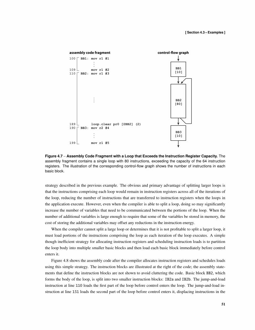
[ Section 4.3 – Examples ]
BB1
BB2
BB3
[10]
[80]
[10]
BB1:
BB2:
BB3:loop.clear pr0 [@BB2] (2)mov r2 #4
mov r1 #3
mov r1 #1
mov r1 #2
mov r1 #5
......
100
109110
189190
199
...
assembly code fragment control-!ow graph
Figure 4.7 – Assembly Code Fragment with a Loop that Exceeds the Instruction Register Capacity. Theassembly fragment contains a single loop with 80 instructions, exceeding the capacity of the 64 instructionregisters. The illustration of the corresponding control-flow graph shows the number of instructions in eachbasic block.
strategy described in the previous example. The obvious and primary advantage of splitting larger loops isthat the instructions comprising each loop would remain in instruction registers across all of the iterations ofthe loop, reducing the number of instructions that are transferred to instruction registers when the loops inthe application execute. However, even when the compiler is able to split a loop, doing so may significantlyincrease the number of variables that need to be communicated between the portions of the loop. When thenumber of additional variables is large enough to require that some of the variables be stored in memory, thecost of storing the additional variables may offset any reductions in the instruction energy.
When the compiler cannot split a large loop or determines that it is not profitable to split a larger loop, itmust load portions of the instructions comprising the loop as each iteration of the loop executes. A simplethough inefficient strategy for allocating instruction registers and scheduling instruction loads is to partitionthe loop body into multiple smaller basic blocks and then load each basic block immediately before controlenters it.
Figure 4.8 shows the assembly code after the compiler allocates instruction registers and schedules loadsusing this simple strategy. The instruction blocks are illustrated at the right of the code; the assembly state-ments that define the instruction blocks are not shown to avoid cluttering the code. Basic block BB2, whichforms the body of the loop, is split into two smaller instruction blocks: IB2a and IB2b. The jump-and-loadinstruction at line 110 loads the first part of the loop before control enters the loop. The jump-and-load in-struction at line 151 loads the second part of the loop before control enters it, displacing instructions in the
51
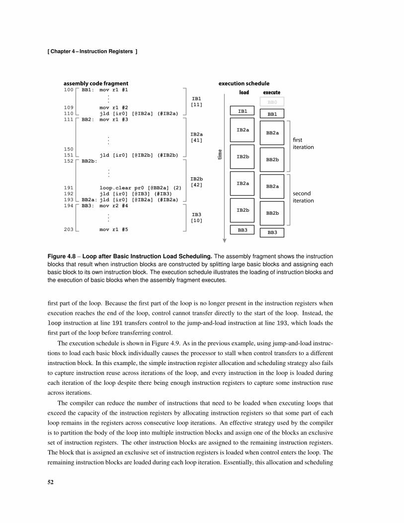
[ Chapter 4 – Instruction Registers ]
BB1:
BB2:
BB3:
loop.clear pr0 [@BB2a] (2)
mov r2 #4
mov r1 #3
mov r1 #1
mov r1 #2
mov r1 #5
......
100
109110
192
194
203
...
jld [ir0] [@IB3] (#IB3)jld [ir0] [@IB2a] (#IB2a)
jld [ir0] [@IB2b] (#IB2b)
jld [ir0] [@IB2a] (#IB2a)111
BB2a:
151150
152
191
193
IB2a
IB2b
BB2b:
IB3
IB1 BB1
BB2a
BB0
IB2a
IB1
IB2b BB2b
BB2aIB2a
IB2b BB2b
BB3 BB3
!rstiteration
seconditeration
[11]
[41]
[42]
[10]
load executeassembly code fragment execution schedule
time
...
Figure 4.8 – Loop after Basic Instruction Load Scheduling. The assembly fragment shows the instructionblocks that result when instruction blocks are constructed by splitting large basic blocks and assigning eachbasic block to its own instruction block. The execution schedule illustrates the loading of instruction blocks andthe execution of basic blocks when the assembly fragment executes.
first part of the loop. Because the first part of the loop is no longer present in the instruction registers whenexecution reaches the end of the loop, control cannot transfer directly to the start of the loop. Instead, theloop instruction at line 191 transfers control to the jump-and-load instruction at line 193, which loads thefirst part of the loop before transferring control.
The execution schedule is shown in Figure 4.9. As in the previous example, using jump-and-load instruc-tions to load each basic block individually causes the processor to stall when control transfers to a differentinstruction block. In this example, the simple instruction register allocation and scheduling strategy also failsto capture instruction reuse across iterations of the loop, and every instruction in the loop is loaded duringeach iteration of the loop despite there being enough instruction registers to capture some instruction ruseacross iterations.
The compiler can reduce the number of instructions that need to be loaded when executing loops thatexceed the capacity of the instruction registers by allocating instruction registers so that some part of eachloop remains in the registers across consecutive loop iterations. An effective strategy used by the compileris to partition the body of the loop into multiple instruction blocks and assign one of the blocks an exclusiveset of instruction registers. The other instruction blocks are assigned to the remaining instruction registers.The block that is assigned an exclusive set of instruction registers is loaded when control enters the loop. Theremaining instruction blocks are loaded during each loop iteration. Essentially, this allocation and scheduling
52

[ Section 4.3 – Examples ]
BB1
BB2a
BB3
BB1:
BB2a:
BB3:loop.clear pr0 [@BB2a] (2)mov r2 #4
mov r1 #3
mov r1 #1
mov r1 #2
mov r1 #5
......
...
100
109110
189190
199
[10]
[43]
[10]
BB2a[18]
BB2b[19]
152153
171170 add r2 r1 #2
...
add r2 r1 #4
...
add r2 r1 #2add r2 r1 #1
BB2b:
BB2c:
assembly code fragment control-!ow graph
Figure 4.9 – Assembly Code After Partitioning Loop Body Into 3 Basic Blocks. The assembly fragmentshows the basic blocks that result when the loop is partitioned into 3 basic blocks. The illustration of thecontrol-flow graph shows the number of instruction pairs in each basic block.
strategy locks one of the instruction blocks in the instruction registers and sequences the remaining instruc-tions through the remaining instruction registers.
Figure 4.9 shows the assembly code fragment with the body of the loop split into three basic blocks:BB2a, BB2b, and BB2c. The updated control-flow graph, annotated with the sizes of the basic blocks, isalso illustrated in Figure 4.9. Though the sizes of the basic blocks might appear arbitrary, the partitioning ofthe loop body shown in the code fragment minimizes the number of instructions that are loaded during eachiteration of the loop when the straight-line loop is split into three blocks. For now, we defer describing a moregeneral approach to determining the number of blocks a loop should be split into and the size of the blocksuntil the subsequent section on instruction register scheduling and allocation, which follows the remainingexamples.
Figure 4.10 shows the code produced by the compiler after instruction register allocation and scheduling.The instruction blocks are illustrated at the right of the assembly code; the assembly statements that definethe instruction blocks are not shown to avoid cluttering the code. The jump-and-load instruction at line 110
loads basic block BB2 and transfers control to the loop. The jump-and-load instruction at line 111 loadsbasic block BB3 when the loop terminates. The code as shown assumes that the jump-and-load instructionat line 111 is loaded to instruction register ir63, which is preserved throughout the execution of the loop.
53

[ Chapter 4 – Instruction Registers ]
BB1:
BB2a:
BB3:loop.clear pr0 [ir0] (2)mov r2 #4
mov r1 #3
mov r1 #1
mov r1 #2
mov r1 #5
......
...
100
111112
193194
203
155156
175
173 add r2 r1 #2
...
add r2 r1 #4
...
add r2 r1 #2add r2 r1 #1
BB2b:
BB2c:
ild [ir44] [@IB2b] (#IB2b)
jld [ir44] [@IB2c] (#IB2c)
jld [ir0] [@IB3] (#IB3)jld [ir0] [@IB2a] (#IB2a)
IB2a[44]
IB2b[19]
IB2c[19]
174
109110
IB3[10]
IB1 BB1
BB2a
BB0
IB2a
154
IB2bBB2b
IB2cBB2c
BB2a
BB2b
BB2c
IB2b
IB2c
IB3 BB3
IB1[12]
!rstiteration
seconditeration
load executeassembly code fragment execution schedule
time
Figure 4.10 – Assembly Code After Load Scheduling. The assembly fragment shows the basic blocks andcorresponding instruction blocks after instruction load and jump-and-load operations are scheduled. The exe-cution schedule illustrates the loading of instruction blocks and execution of basic blocks when the assemblyfragment executes.
Basic block BB2 is loaded when control first enters the loop and remains in the instruction registers until theloop completes. Basic blocks BB2a and BB2b are loaded during each iteration of the loop, and use the sameinstruction registers.
The ild instruction at line 154 loads basic block BB2b at instruction register ir44, immediately afterBB2a in the instruction register file. This allows control to fall through to BB2b when the add instruction atline 155 executes from instruction register ir43. The load instruction at line 154 could appear earlier in thecode to allow more time for the instruction register management unit to initiate the instruction load. The jump-and-load instruction at line 174 loads basic block BB2c and then transfers control to it. The loop instructionat line 193 executes from instruction register ir63. When the loop is repeated, the loop instruction transferscontrol to instruction register ir0, which contains the first instruction of BB2. When the loop terminates,control falls through to instruction register ir63, which contains the jump-and-load instruction at line 111.The jump-and-load instruction loads basic block BB3 and transfers control to it.
The execution schedule for the code is shown in Figure 4.10. As illustrated, instruction block IB2a isloaded once when control enters the loop and resides in the instruction registers for the duration of the loop.Instruction blocks IB2b and IB2c are loaded during every iteration of the loop. The code shown in Fig-ure 4.10 loads 83 instructions during the first iteration of the loop and 38 instruction during each subsequent
54
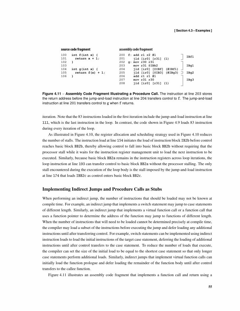
[ Section 4.3 – Examples ]
add r1 r2 #1 jld [ir0] [r31] (1)
f: 200201 IBf1
g:mov r31 @IBk2mov r30 r31
jld [ir0] [@IBf] (#IBf1)jld [ir0] [@IB3] (#IBg3)add r1 r1 #1
IBg2
IBg1
IBg3mov r31 r30jld [ir0] [r31] (1)
100101102
int g(int x) {return f(x) + 1;
}
int f(int x) {return x + 1;
103104105
}106
202203204205206207208
assembly code fragmentsource code fragment
Figure 4.11 – Assembly Code Fragment Illustrating a Procedure Call. The instruction at line 203 storesthe return address before the jump-and-load instruction at line 204 transfers control to f. The jump-and-loadinstruction at line 201 transfers control to g when f returns.
iteration. Note that the 83 instructions loaded in the first iteration include the jump-and-load instruction at line111, which is the last instruction in the loop. In contrast, the code shown in Figure 4.9 loads 83 instructionduring every iteration of the loop.
As illustrated in Figure 4.10, the register allocation and scheduling strategy used in Figure 4.10 reducesthe number of stalls. The instruction load at line 154 initiates the load of instruction block IB2b before controlreaches basic block BB2b, thereby allowing control to fall into basic block BB2b without requiring that theprocessor stall while it waits for the instruction register management unit to load the next instruction to beexecuted. Similarly, because basic block BB2a remains in the instruction registers across loop iterations, theloop instruction at line 193 can transfer control to basic block BB2a without the processor stalling. The onlystall encountered during the execution of the loop body is the stall imposed by the jump-and-load instructionat line 174 that loads IBB2c as control enters basic block BB2c.
Implementing Indirect Jumps and Procedure Calls as Stubs
When performing an indirect jump, the number of instructions that should be loaded may not be known atcompile time. For example, an indirect jump that implements a switch statement may jump to case statementsof different length. Similarly, an indirect jump that implements a virtual function call or a function call thatuses a function pointer to determine the address of the function may jump to functions of different length.When the number of instructions that will need to be loaded cannot be determined precisely at compile time,the compiler may load a subset of the instructions before executing the jump and defer loading any additionalinstructions until after transferring control. For example, switch statements can be implemented using indirectinstruction loads to load the initial instructions of the target case statement, deferring the loading of additionalinstructions until after control transfers to the case statement. To reduce the number of loads that execute,the compiler can set the size of the initial load to be equal to the shortest case statement so that only longercase statements perform additional loads. Similarly, indirect jumps that implement virtual function calls caninitially load the function prologue and defer loading the remainder of the function body until after controltransfers to the callee function.
Figure 4.11 illustrates an assembly code fragment that implements a function call and return using a
55
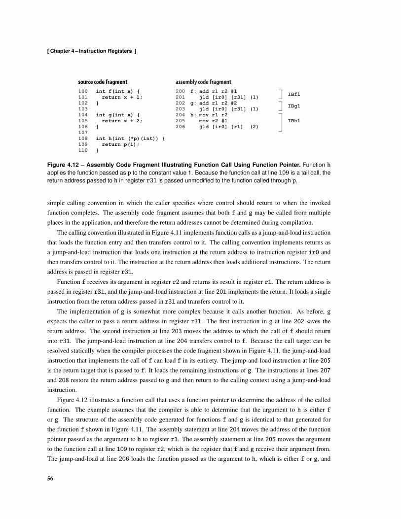
[ Chapter 4 – Instruction Registers ]
int h(int (*p)(int)) {return p(1);
}
add r1 r2 #1 f: IBf1
add r1 r2 #2 g: IBg1
jld [ir0] [r1] (2)
h: mov r2 #1mov r1 r2
IBh1
jld [ir0] [r31] (1)
jld [ir0] [r31] (1)
100101102
int g(int x) {return x + 2;
}
int f(int x) {return x + 1;
103104105
}106107108109110
200201202203204205206
assembly code fragmentsource code fragment
Figure 4.12 – Assembly Code Fragment Illustrating Function Call Using Function Pointer. Function happlies the function passed as p to the constant value 1. Because the function call at line 109 is a tail call, thereturn address passed to h in register r31 is passed unmodified to the function called through p.
simple calling convention in which the caller specifies where control should return to when the invokedfunction completes. The assembly code fragment assumes that both f and g may be called from multipleplaces in the application, and therefore the return addresses cannot be determined during compilation.
The calling convention illustrated in Figure 4.11 implements function calls as a jump-and-load instructionthat loads the function entry and then transfers control to it. The calling convention implements returns asa jump-and-load instruction that loads one instruction at the return address to instruction register ir0 andthen transfers control to it. The instruction at the return address then loads additional instructions. The returnaddress is passed in register r31.
Function f receives its argument in register r2 and returns its result in register r1. The return address ispassed in register r31, and the jump-and-load instruction at line 201 implements the return. It loads a singleinstruction from the return address passed in r31 and transfers control to it.
The implementation of g is somewhat more complex because it calls another function. As before, gexpects the caller to pass a return address in register r31. The first instruction in g at line 202 saves thereturn address. The second instruction at line 203 moves the address to which the call of f should returninto r31. The jump-and-load instruction at line 204 transfers control to f. Because the call target can beresolved statically when the compiler processes the code fragment shown in Figure 4.11, the jump-and-loadinstruction that implements the call of f can load f in its entirety. The jump-and-load instruction at line 205is the return target that is passed to f. It loads the remaining instructions of g. The instructions at lines 207and 208 restore the return address passed to g and then return to the calling context using a jump-and-loadinstruction.
Figure 4.12 illustrates a function call that uses a function pointer to determine the address of the calledfunction. The example assumes that the compiler is able to determine that the argument to h is either for g. The structure of the assembly code generated for functions f and g is identical to that generated forthe function f shown in Figure 4.11. The assembly statement at line 204 moves the address of the functionpointer passed as the argument to h to register r1. The assembly statement at line 205 moves the argumentto the function call at line 109 to register r2, which is the register that f and g receive their argument from.The jump-and-load at line 206 loads the function passed as the argument to h, which is either f or g, and
56
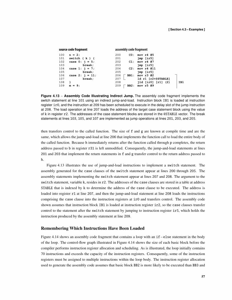
[ Section 4.3 – Examples ]
m = 9;
ld r1 [r2+@STABLE]jld [ir0] [r1] (2)
mov r4 #5jmp [ir5]mov r4 #7jmp [ir5]mov r4 #11jmp [ir5]
C0:
C1:
C2:
mov r5 #9
mov r3 #2BB1:
BB2:IB1
assembly code fragmentsource code fragment100101102103104105106107108109
n = 2;switch ( k ) {case 0: j = 5;
break;case 1: j = 7;
break;case 2: j = 11;
break;}
200201202203204205206207208209
Figure 4.13 – Assembly Code Illustrating Indirect Jump. The assembly code fragment implements theswitch statement at line 101 using an indirect jump-and-load. Instruction block IB1 is loaded at instructionregister ir0, and the instruction at 209 has been scheduled to execute in the delay slot of the jump instructionat 208. The load operation at line 207 loads the address of the target case statement block using the valueof k in register r2. The addresses of the case statement blocks are stored in the @STABLE vector. The breakstatements at lines 103, 105, and 107 are implemented as jump operations at lines 201, 203, and 205.
then transfers control to the called function. The size of f and g are known at compile time and are thesame, which allows the jump-and-load at line 206 that implements the function call to load the entire body ofthe called function. Because h immediately returns after the function called through p completes, the returnaddress passed to b in register r31 is left unmodified. Consequently, the jump-and-load statements at lines201 and 203 that implement the return statements in f and g transfer control to the return address passed toh.
Figure 4.13 illustrates the use of jump-and-load instructions to implement a switch statement. Theassembly generated for the case clauses of the switch statement appear at lines 200 through 205. Theassembly statements implementing the switch statement appear at lines 207 and 208. The argument to theswitch statement, variable k, resides in r2. The addresses of the case clauses are stored in a table at addressSTABLE that is indexed by k to determine the address of the case clause to be executed. The address isloaded into register r1 at line 207, and then the jump-and-load statement at line 208 loads the instructionscomprising the case clause into the instruction registers at ir0 and transfers control. The assembly codeshown assumes that instruction block IB1 is loaded at instruction register ir2, so the case clauses transfercontrol to the statement after the switch statement by jumping to instruction register ir5, which holds theinstruction produced by the assembly statement at line 209.
Remembering Which Instructions Have Been Loaded
Figure 4.14 shows an assembly code fragment that contains a loop with an if – else statement in the bodyof the loop. The control-flow graph illustrated in Figure 4.14 shows the size of each basic block before thecompiler performs instruction register allocation and scheduling. As is illustrated, the loop initially contains70 instructions and exceeds the capacity of the instruction registers. Consequently, some of the instructionregisters must be assigned to multiple instructions within the loop body. The instruction register allocationused to generate the assembly code assumes that basic block BB2 is more likely to be executed than BB3 and
57
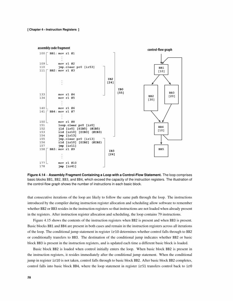
[ Chapter 4 – Instruction Registers ]
BB1[10]
BB2[30]
BB3[20]
BB4[10]
BB5
BB1: mov r1 #1
mov r1 #2
...
100
jmp.clear pr0 [ir53] 109110
BB2: mov r1 #3
...
mov r1 #4
...
mov r1 #5
mov r1 #6
111
...
BB4: mov r1 #7
mov r1 #8loop.clear pr0 [ir0]jld [ir0] [@IB5] (#IB5)ild [ir10] [@IB3] (#IB3) jmp [ir13]
140
133134
141
151150
152153154
BB3:
jmp [ir41]...
mov r1 #9
mov r1 #10
jmp.clear pr0 [ir13] ild [ir10] [@IB2] (#IB2)jmp [ir11]
155156157158
178177
IB0[55]
IB2[24]
IB3[24]
assembly code fragment control-!ow graph
Figure 4.14 – Assembly Fragment Containing a Loop with a Control-Flow Statement. The loop comprisesbasic blocks BB1, BB2, BB3, and BB4, which exceed the capacity of the instruction registers. The illustration ofthe control-flow graph shows the number of instructions in each basic block.
that consecutive iterations of the loop are likely to follow the same path through the loop. The instructionsintroduced by the compiler during instruction register allocation and scheduling allow software to rememberwhether BB2 or BB3 resides in the instruction registers so that instructions are not loaded when already presentin the registers. After instruction register allocation and scheduling, the loop contains 79 instructions.
Figure 4.15 shows the contents of the instruction registers when BB2 is present and when BB3 is present.Basic blocks BB1 and BB4 are present in both cases and remain in the instruction registers across all iterationsof the loop. The conditional jump statement in register ir10 determines whether control falls through to BB2
or conditionally transfers to BB3. The destination of the conditional jump indicates whether BB2 or basicblock BB3 is present in the instruction registers, and is updated each time a different basic block is loaded.
Basic block BB2 is loaded when control initially enters the loop. When basic block BB2 is present inthe instruction registers, it resides immediately after the conditional jump statement. When the conditionaljump in register ir10 is not taken, control falls through to basic block BB2. After basic block BB2 completes,control falls into basic block BB4, where the loop statement in register ir51 transfers control back to ir0
58
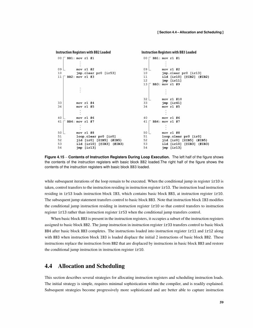
[ Section 4.4 – Allocation and Scheduling ]
BB1: mov r1 #1
mov r1 #2
...
00
jmp.clear pr0 [ir53] 0910
BB2: mov r1 #3
...
mov r1 #4
...
mov r1 #5
mov r1 #6
11
...
BB4: mov r1 #7
mov r1 #8loop.clear pr0 [ir0]jld [ir0] [@IB5] (#IB5)ild [ir10] [@IB3] (#IB3) jmp [ir13]
BB1: mov r1 #1
mov r1 #2
...
00
jmp.clear pr0 [ir13] 0910
ild [ir10] [@IB2] (#IB2)jmp [ir11]
1112
BB3:13
mov r1 #6
...
BB4: mov r1 #7
mov r1 #8loop.clear pr0 [ir0]jld [ir0] [@IB5] (#IB5)ild [ir10] [@IB3] (#IB3) jmp [ir13]
jmp [ir41]
......
mov r1 #9
mov r1 #103233
mov r1 #534
40
3334
414041
5150
525354
5150
525354
Instruction Registers with BB2 Loaded Instruction Registers with BB3 Loaded
Figure 4.15 – Contents of Instruction Registers During Loop Execution. The left half of the figure showsthe contents of the instruction registers with basic block BB2 loaded.The right half of the figure shows thecontents of the instruction registers with basic block BB3 loaded.
while subsequent iterations of the loop remain to be executed. When the conditional jump in register ir10 istaken, control transfers to the instruction residing in instruction register ir53. The instruction load instructionresiding in ir53 loads instruction block IB3, which contains basic block BB3, at instruction register ir10.The subsequent jump statement transfers control to basic block BB3. Note that instruction block IB3 modifiesthe conditional jump instruction residing in instruction register ir10 so that control transfers to instructionregister ir13 rather than instruction register ir53 when the conditional jump transfers control.
When basic block BB3 is present in the instruction registers, it occupies a subset of the instruction registersassigned to basic block BB2. The jump instruction in instruction register ir33 transfers control to basic blockBB4 after basic block BB3 completes. The instructions loaded into instruction register ir11 and ir12 alongwith BB3 when instruction block IB3 is loaded displace the initial 2 instructions of basic block BB2. Theseinstructions replace the instruction from BB2 that are displaced by instructions in basic block BB3 and restorethe conditional jump instruction in instruction register ir10.
4.4 Allocation and Scheduling
This section describes several strategies for allocating instruction registers and scheduling instruction loads.The initial strategy is simple, requires minimal sophistication within the compiler, and is readily explained.Subsequent strategies become progressively more sophisticated and are better able to capture instruction
59
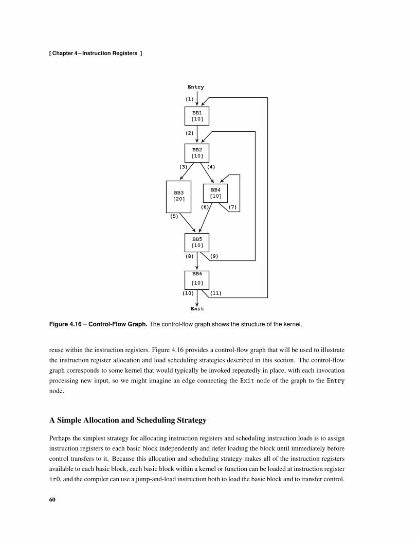
[ Chapter 4 – Instruction Registers ]
BB6
[10]
BB5[10]
BB2[10]
BB3[20]
BB4[10]
BB1[10]
(1)
(2)
(3) (4)
(5)
(6) (7)
(8)
(10)
Entry
Exit
(9)
(11)
Figure 4.16 – Control-Flow Graph. The control-flow graph shows the structure of the kernel.
reuse within the instruction registers. Figure 4.16 provides a control-flow graph that will be used to illustratethe instruction register allocation and load scheduling strategies described in this section. The control-flowgraph corresponds to some kernel that would typically be invoked repeatedly in place, with each invocationprocessing new input, so we might imagine an edge connecting the Exit node of the graph to the Entry
node.
A Simple Allocation and Scheduling Strategy
Perhaps the simplest strategy for allocating instruction registers and scheduling instruction loads is to assigninstruction registers to each basic block independently and defer loading the block until immediately beforecontrol transfers to it. Because this allocation and scheduling strategy makes all of the instruction registersavailable to each basic block, each basic block within a kernel or function can be loaded at instruction registerir0, and the compiler can use a jump-and-load instruction both to load the basic block and to transfer control.
60
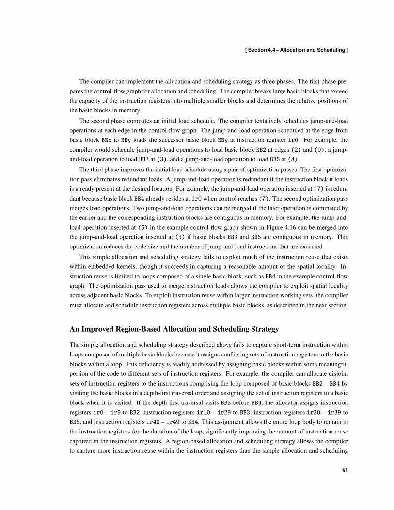
[ Section 4.4 – Allocation and Scheduling ]
The compiler can implement the allocation and scheduling strategy as three phases. The first phase pre-pares the control-flow graph for allocation and scheduling. The compiler breaks large basic blocks that exceedthe capacity of the instruction registers into multiple smaller blocks and determines the relative positions ofthe basic blocks in memory.
The second phase computes an initial load schedule. The compiler tentatively schedules jump-and-loadoperations at each edge in the control-flow graph. The jump-and-load operation scheduled at the edge frombasic block BBx to BBy loads the successor basic block BBy at instruction register ir0. For example, thecompiler would schedule jump-and-load operations to load basic block BB2 at edges (2) and (9), a jump-and-load operation to load BB3 at (3), and a jump-and-load operation to load BB5 at (8).
The third phase improves the initial load schedule using a pair of optimization passes. The first optimiza-tion pass eliminates redundant loads. A jump-and-load operation is redundant if the instruction block it loadsis already present at the desired location. For example, the jump-and-load operation inserted at (7) is redun-dant because basic block BB4 already resides at ir0 when control reaches (7). The second optimization passmerges load operations. Two jump-and-load operations can be merged if the later operation is dominated bythe earlier and the corresponding instruction blocks are contiguous in memory. For example, the jump-and-load operation inserted at (5) in the example control-flow graph shown in Figure 4.16 can be merged intothe jump-and-load operation inserted at (3) if basic blocks BB3 and BB5 are contiguous in memory. Thisoptimization reduces the code size and the number of jump-and-load instructions that are executed.
This simple allocation and scheduling strategy fails to exploit much of the instruction reuse that existswithin embedded kernels, though it succeeds in capturing a reasonable amount of the spatial locality. In-struction reuse is limited to loops composed of a single basic block, such as BB4 in the example control-flowgraph. The optimization pass used to merge instruction loads allows the compiler to exploit spatial localityacross adjacent basic blocks. To exploit instruction reuse within larger instruction working sets, the compilermust allocate and schedule instruction registers across multiple basic blocks, as described in the next section.
An Improved Region-Based Allocation and Scheduling Strategy
The simple allocation and scheduling strategy described above fails to capture short-term instruction withinloops composed of multiple basic blocks because it assigns conflicting sets of instruction registers to the basicblocks within a loop. This deficiency is readily addressed by assigning basic blocks within some meaningfulportion of the code to different sets of instruction registers. For example, the compiler can allocate disjointsets of instruction registers to the instructions comprising the loop composed of basic blocks BB2 – BB4 byvisiting the basic blocks in a depth-first traversal order and assigning the set of instruction registers to a basicblock when it is visited. If the depth-first traversal visits BB3 before BB4, the allocator assigns instructionregisters ir0 – ir9 to BB2, instruction registers ir10 – ir29 to BB3, instruction registers ir30 – ir39 toBB5, and instruction registers ir40 – ir49 to BB4. This assignment allows the entire loop body to remain inthe instruction registers for the duration of the loop, significantly improving the amount of instruction reusecaptured in the instruction registers. A region-based allocation and scheduling strategy allows the compilerto capture more instruction reuse within the instruction registers than the simple allocation and scheduling
61
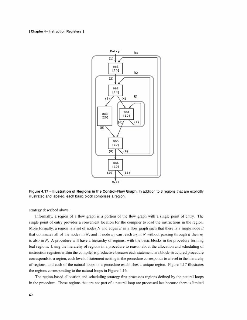
[ Chapter 4 – Instruction Registers ]
R1
R2
R3
BB6[10]
BB5[10]
BB2[10]
BB3[20]
BB4[10]
BB1[10]
(1)
(2)
(3) (4)
(5)
(6) (7)
(8)
(10)
Entry
Exit
(9)
(11)
Figure 4.17 – Illustration of Regions in the Control-Flow Graph. In addition to 3 regions that are explicitlyillustrated and labeled, each basic block comprises a region.
strategy described above.
Informally, a region of a flow graph is a portion of the flow graph with a single point of entry. Thesingle point of entry provides a convenient location for the compiler to load the instructions in the region.More formally, a region is a set of nodes N and edges E in a flow graph such that there is a single node d
that dominates all of the nodes in N, and if node n1 can reach n2 in N without passing through d then n1
is also in N. A procedure will have a hierarchy of regions, with the basic blocks in the procedure formingleaf regions. Using the hierarchy of regions in a procedure to reason about the allocation and scheduling ofinstruction registers within the compiler is productive because each statement in a block-structured procedurecorresponds to a region, each level of statement nesting in the procedure corresponds to a level in the hierarchyof regions, and each of the natural loops in a procedure establishes a unique region. Figure 4.17 illustratesthe regions corresponding to the natural loops in Figure 4.16.
The region-based allocation and scheduling strategy first processes regions defined by the natural loopsin the procedure. Those regions that are not part of a natural loop are processed last because there is limited
62
[ Section 4.4 – Allocation and Scheduling ]
or no opportunity for instruction reuse within these regions. The allocator sorts the regions so that smallerregions that are closer to the leaf regions in the hierarchy of regions are processed before larger enclosingregions. This ensures that instructions in inner loops are assigned instruction registers before instructions inenclosing loops.
Allocating instruction registers within larger regions allows the instructions in the regions to be assignedto contiguous sets of instruction registers. This reduces the number of instruction load operations that arerequired to load composite instructions regions. Before processing a region, the allocator attempts to expandthe allocation region into the immediately enclosing region. A region is expanded when the enclosing regionis small enough to fit in the instruction registers. For example, when processing the procedure illustrated inFigure 4.17, the allocator would begin with process region R1. The allocator would expand the allocation re-gion to R2, which contains 50 instructions. The allocator cannot further expand the allocation region becauseregion R3, the enclosing region in the hierarchy of regions, contains 70 instructions and exceeds the capacityof the instruction registers.
After expanding the allocation region, the allocator tentatively assigns instruction registers to the basicblocks in the region based on a depth-first traversal of the basic blocks in the region. The assignment istentative in that it may later be repositioned, though the relative positions of the instructions within the regionwill not change. For example, the allocator would tentatively assign instruction registers ir0 – ir49 to thebasic blocks in region R2. Instruction registers ir0 – ir9 would be assigned to BB2, instruction registersir10 – ir29 to BB3, instruction registers ir30 – ir39 to BB4, and instruction registers ir40 – ir49 to BB5.
When a region exceeds the capacity of the instruction registers, the allocator attempts to assign instructionregisters not used in any of the enclosed regions that were previously processed and assigned registers. Forexample, region R3 contains more instructions than there are instruction registers. When processing regionR3, the allocator assigns instruction registers ir0 – ir9 to basic block BB1, translates the assignments withinregion R2 so that the region uses registers ir10 – ir59, and assigns instruction registers ir60 – ir63 andir0 – ir5 to basic block BB6.
After the instruction register allocation phase completes, the load scheduling phase inserts load oper-ations. The scheduler first tentatively schedules jump-and-load operations at each basic block, as in theprevious allocation and scheduling strategy. The scheduler then schedules load operations to load regionsthat were allocated contiguous sets of instruction registers at the edges arriving at the dominator node. Theseload operations are inserted to render some of the tentatively scheduled jump-and-load operations redundant.Generally, this strategy of lifting loads closer to the entry point of the procedure is productive because itreduces the number of instruction load operations. However, this strategy may result in some regions beingloaded and not executed, such as when there is a point of divergence in the control-flow graph. The schedulercan defer loading regions that are not certain to be executed until control transfers to the region to avoid this.
Redundant load operations are identified using a data-flow analysis that determines which instructions arecertain to reside in the instruction registers at each point in the code. The values computed by the data-flowanalysis are sets of instructions, referred to as the resident instruction sets. The data-flow analysis initializesthe resident instruction sets to the empty set. The transfer function used in the data-flow analysis updatesthe resident instruction sets when load operations are encountered. The instructions that are loaded by the
63

[ Chapter 4 – Instruction Registers ]
BB6[10]
BB5[10]
BB2[10]
BB3[20]
BB4[10]
BB1[10]
(BB3) (BB4)
(BB5)
(BB5)
(BB6)
Entry
Exit
(BB2BB5)
BB6[10]
BB5[10]
BB2[10]
BB3[20]
BB4[10]
BB1[10]
Entry
Exit
Initial Load Schedule Resident Instruction Sets
(BB2BB5)
(BB4)
(BB1BB5)
(BB1BB5)
{}
{BB1BB5}
{BB1BB5}
{BB1BB5} {BB1BB5}
{BB1BB5}
{BB2BB6}
BB6[10]
BB5[10]
BB2[10]
BB3[20]
BB4[10]
BB1[10]
(BB6)
Entry
Exit
(BB1BB5)
(BB1)
Final Load Schedule
Figure 4.18 – Resident Instruction Sets. The control-flow graph at the left shows the initial load schedule.The edges of the control-flow graph are annotated with the basic blocks that the compiler has scheduled to beloaded when control transfers between the basic blocks incident on the edge. The resident instruction sets forthe initial load schedule are shown on the control-flow graph in the middle. Each basic block is annotated withthe set of basic blocks that are in the resident instruction set computed for the basic block. The control-flowgraph at the right shows the revised load schedule.
load operation are added to the resident instruction set, and any instructions that are displaced by the loadoperation are removed. The meet operator used to combine data-flow values at convergence points computesthe intersection of the resident instruction sets over the converging paths. This ensures that only those in-structions that are present at all incoming paths are added to the resident instruction set. After computingthe resident instruction sets, the load scheduler optimizes the load schedule by eliminating any loads thatare redundant. A load is redundant if it loads an instruction block that is already present, as computed bythe resident instruction set data-flow analysis. Figure 4.18 illustrates the initial load schedule, the residentinstruction sets computed by the data-flow analysis, and the optimized load schedule.
64
[ Section 4.4 – Allocation and Scheduling ]
Improving Instruction Reuse Within Large Allocation Regions
The amount of instruction reuse captured in the instruction registers when executing loops that exceed thecapacity of the instruction registers can be improved by extending the region-based allocation strategy de-scribed above. The basic idea is to partition the instruction registers into two disjoint sets. Registers in thefirst set are assigned to instructions that reside in registers for the duration of the loop. Registers in the secondset are assigned to instructions that are loaded while the loop executes. We sometimes describe registersin the second set as non-exclusive within the code region because they are shared by multiple instructions.Similarly, we sometimes describe registers in the first set as exclusive within the code region.
The concepts behind the extension were explored previously using the loop contained in the code fragmentshown in Figure 4.7 as an example. The compiler improves the effectiveness of the allocation strategy byselecting instructions that are executed more frequently for inclusion in the set of instructions that are assignedexclusive registers. For example, within region R2 of the control-flow graph shown in Figure 4.17, basicblocks BB2 and BB5 are certain to be executed during every iteration of the loop, whereas only one of BB3and BB4 will be executed during each iteration. Consequently, instructions in basic blocks BB2 and BB5 arebetter candidates for inclusion in the set of instructions assigned to exclusive registers than the instructionsin BB3. Similarly, when there are enough non-exclusive registers to accommodate basic block BB4, so thatinstruction reuse within region R1 can be captured in the non-exclusive registers, instructions in basic blocksBB2 and BB5 are better candidates for assignment to exclusive registers than the instructions in BB4.
Let us consider allocating and scheduling instruction registers within a region that corresponds to a loopthat exceeds the instruction register capacity, such as the loop shown in Figure 4.7. The instruction registerallocator will partition the instruction registers into two sets. The first set will be used to hold those instruc-tions that remain in the instruction registers for the duration of the loop; the second set will be used to holdthose instructions that are loaded during each iteration of the loop. We will denote the number of registers inthe first set by r1 and the number in the second set by r2.
The compiler will partition the instructions within the allocation region into n + 2 instruction blocks,where n is a positive integer. The first instruction block will remain in the instruction registers for the durationof the loop; the remaining n + 1 instruction blocks will be loaded during each iteration of the loop. Thus,the first instruction block may contain up to r1 instructions, and the remaining n + 1 instruction blocks maycontain up to r2 instructions. For all but the last region, the compiler must reserve one instruction register forthe load operation that transfers the next instruction block in the loop; an instruction register is not needed inthe last instruction block in the region because the first instruction block remains in the instruction registersacross loop iterations. Thus, the allocator may assume that there are r1−1 instruction registers available forinstructions in the first instruction block, that there are r2−1 instruction registers available for instructions inthe next n instruction blocks, and that there are r2 instruction registers available for instructions in the finalinstruction block. The compiler must also reserve one instruction register to load the region in the control flowgraph that executes after the loop completes. Consequently, if there are R instruction registers available to theallocator, the allocator must choose r1 and r2 such that r1 +r2 < R. Intuitively, the number of instructions thatare loaded during each iteration is minimized when the allocator uses all of the available instruction registers,
65

[ Chapter 4 – Instruction Registers ]
and the allocator should choose r1 and r2 such that r1 + r2 = R−1.The compiler can reduce the number of instructions that are loaded during each iteration of the loop by
selecting n and r2 to minimize
(n+1)r2 (4.1)
subject to the constraints
r1−1+n(r2−1)+ r2 = N (4.2)
r1 + r2 = R−1. (4.3)
Equations (4.2) and (4.3) can be used to derive the following equations for computing r1 and r2 for a givenvalue of n as follows,
r2 = (N−R+2)/n+1 (4.4)
r1 = R− r2−1. (4.5)
Returning to the loop contained in the code fragment shown in Figure 4.7, we can use the above equationsto determine the partitioning of the loop that results in the smallest number of instructions being transferredto the instruction registers. Before instruction register allocation and scheduling, the loop contains 80 instruc-tions. When the allocator is permitted to use all 64 of the instruction registers, we have N = 80 and R = 64.The values of r1 and r2 computed using equations (4.2) and (4.3) for different values of n are tabulated asfollows.
n r2 r1 (n+1)r2
1 19 44 382 10 53 303 7 56 284 6 57 30
From the table we can see that the number of instructions transferred is minimized when n = 3. This requirespartitioning the loop into 5 instruction blocks and allocating 56 instruction registers to those instructions thatremain in the instruction registers through the duration of the loop.
Partitioning a region into more instruction blocks increases number of jump-and-load or instruction loadoperations that need to be scheduled and executed. The compiler may be able to find empty issue slots inwhich it can schedule these operations without increasing the number of instructions in the region. How-ever, the compiler will sometimes find it necessary to extend the instruction schedule to accommodate theadditional instruction register management operations, thereby increasing the code size and execution time.Furthermore, the jump-and-load instructions may introduce additional stall cycles because there is limitedopportunity to hide the instruction load latency with other useful operations. Consequently, when allocatingand scheduling instruction registers, the compiler attempts to balance performance demands against increased
66
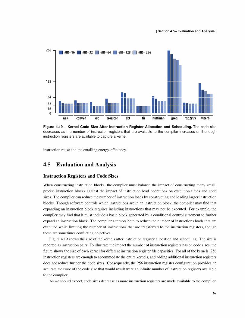
[ Section 4.5 – Evaluation and Analysis ]
64
128
256
1632
0aes conv2d crc crosscor dct !r hu"man jpeg rgb2yuv viterbi
#IR=16 #IR=32 #IR=64 #IR=128 #IR= 256
Figure 4.19 – Kernel Code Size After Instruction Register Allocation and Scheduling. The code sizedecreases as the number of instruction registers that are available to the compiler increases until enoughinstruction registers are available to capture a kernel.
instruction reuse and the entailing energy-efficiency.
4.5 Evaluation and Analysis
Instruction Registers and Code Sizes
When constructing instruction blocks, the compiler must balance the impact of constructing many small,precise instruction blocks against the impact of instruction load operations on execution times and codesizes. The compiler can reduce the number of instruction loads by constructing and loading larger instructionblocks. Though software controls which instructions are in an instruction block, the compiler may find thatexpanding an instruction block requires including instructions that may not be executed. For example, thecompiler may find that it must include a basic block generated by a conditional control statement to furtherexpand an instruction block. The compiler attempts both to reduce the number of instructions loads that areexecuted while limiting the number of instructions that are transferred to the instruction registers, thoughthese are sometimes conflicting objectives.
Figure 4.19 shows the size of the kernels after instruction register allocation and scheduling. The size isreported as instruction pairs. To illustrate the impact the number of instruction registers has on code sizes, thefigure shows the size of each kernel for different instruction register file capacities. For all of the kernels, 256instruction registers are enough to accommodate the entire kernels, and adding additional instruction registersdoes not reduce further the code sizes. Consequently, the 256 instruction register configuration provides anaccurate measure of the code size that would result were an infinite number of instruction registers availableto the compiler.
As we should expect, code sizes decrease as more instruction registers are made available to the compiler.
67
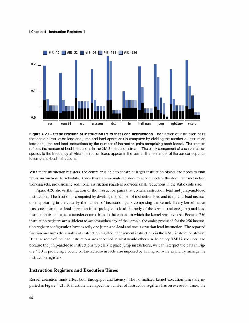
[ Chapter 4 – Instruction Registers ]
aes conv2d crc crosscor dct !r hu"man jpeg rgb2yuv viterbi
#IR=16 #IR=32 #IR=64 #IR=128 #IR= 256
0.0
0.1
0.2
Figure 4.20 – Static Fraction of Instruction Pairs that Load Instructions. The fraction of instruction pairsthat contain instruction load and jump-and-load operations is computed by dividing the number of instructionload and jump-and-load instructions by the number of instruction pairs comprising each kernel. The fractionreflects the number of load instructions in the XMU instruction stream. The black component of each bar corre-sponds to the frequency at which instruction loads appear in the kernel; the remainder of the bar correspondsto jump-and-load instructions.
With more instruction registers, the compiler is able to construct larger instruction blocks and needs to emitfewer instructions to schedule. Once there are enough registers to accommodate the dominant instructionworking sets, provisioning additional instruction registers provides small reductions in the static code size.
Figure 4.20 shows the fraction of the instruction pairs that contain instruction load and jump-and-loadinstructions. The fraction is computed by dividing the number of instruction load and jump-and-load instruc-tions appearing in the code by the number of instruction pairs comprising the kernel. Every kernel has atleast one instruction load operation in its prologue to load the body of the kernel, and one jump-and-loadinstruction its epilogue to transfer control back to the context in which the kernel was invoked. Because 256instruction registers are sufficient to accommodate any of the kernels, the codes produced for the 256 instruc-tion register configuration have exactly one jump-and-load and one instruction load instruction. The reportedfraction measures the number of instruction register management instructions in the XMU instruction stream.Because some of the load instructions are scheduled in what would otherwise be empty XMU issue slots, andbecause the jump-and-load instructions typically replace jump instructions, we can interpret the data in Fig-ure 4.20 as providing a bound on the increase in code size imposed by having software explicitly manage theinstruction registers.
Instruction Registers and Execution Times
Kernel execution times affect both throughput and latency. The normalized kernel execution times are re-ported in Figure 4.21. To illustrate the impact the number of instruction registers has on execution times, the
68

[ Section 4.5 – Evaluation and Analysis ]
#IR=16 #IR=32 #IR=64 #IR=128 #IR= 256
aes conv2d crc crosscor dct !r hu"man jpeg rgb2yuv viterbi0.0
0.5
1.0
1.5
2.0
Figure 4.21 – Normalized Kernel Execution Time. The kernel execution time decreases as the number ofinstruction registers that are available to the compiler increases until there are enough instruction registers tocapture a kernel.
figure shows the execution times for different instruction register file capacities.
As we should expect, the execution times decrease as more instruction registers are made available tothe compiler. With more instruction registers, fewer instructions need to be loaded during the execution of akernel, and the processor spends less time stalled waiting for instructions to arrive. The additional instructionregisters allow the compiler to construct larger instruction blocks, which reduces the number of instructionload operations that the compiler needs to schedule.
Instruction loads compete with other instructions for XMU issue slots, and may displace compute in-structions. Figure 4.22 shows the fraction of the XMU issue slots that are occupied by instruction load andjump-and-load instructions. The reported fraction is computed by dividing the number of instruction loadand jump-and-load instructions executed during a kernel by the number of instruction pairs issued during theexecution of the kernel.
As Figure 4.22 illustrates, the fraction of issue slots consumed by instruction loads decreases as more in-struction registers are made available to the compiler. Intuitively, this results because the compiler is able toconstruct larger instruction blocks and consequently needs to issue fewer instruction loads. The abrupt reduc-tions in the fraction of issue slots occupied by load instructions we observe when the number of instructionregisters exceeds some critical threshold is explained by how the compiler constructions instruction blocksand schedules instruction loads. The compiler attempts to advance instruction loads above loops. Conse-quently, when the compiler has enough instruction registers available to lift a load out of a loop, the fractionof issue slots occupied by instruction loads decreases by an amount that is proportionate to the contributionof the loop to the execution time.
The data presented in Figure 4.22 explains part of the increase in execution times we observe when wereduce the number of instruction registers and is illustrated in Figure 4.21. Kernels take longer to execute
69

[ Chapter 4 – Instruction Registers ]
aes conv2d crc crosscor dct !r hu"man jpeg rgb2yuv viterbi
#IR=16 #IR=32 #IR=64 #IR=128 #IR= 256
0.0
0.1
0.2
Figure 4.22 – Fraction of Issued Instruction Pairs that Contain Instruction Loads. The reported fraction iscomputed by dividing the number of instruction load and jump-and-load instructions executed during a kernelby the number of instruction pairs issued during the execution of the kernel.
when there are fewer instruction registers because more time is lost executing load instructions. The remain-der of the increase in execution time is due to the processor waiting for instructions to arrive from memory.The processor spends more time waiting for instructions when the instruction register file capacity is reducedbecause instructions are loaded more often and individual transfers are shorter, providing less time to overlapinstruction transfers and computation.
Instruction Bandwidth
Figure 4.23 shows the normalized instruction bandwidth demand at the instruction register file and memory.The normalized instruction bandwidth demand measures the ratio of the instruction bandwidth demand at theinstruction register files and the local memory interface. We can interpret it as an estimate of the number ofinstruction pairs that need to be delivered from the instruction register files and memory each cycle to meetthe instruction demands of the processor. The instruction bandwidths are normalized to remove the impactof stalls introduced by data communication. The differences in the instruction bandwidth demands measuredfor the different kernels and capacities provide insights into the spatial and temporal locality present in theinstruction accesses scheduled by the compiler.
As Figure 4.23 illustrates, the normalized instruction bandwidth demand at the instruction register filesdoes not depend on the number of instruction registers, as the demand is determined by the rate at whichthe processor requests instructions from the instruction registers. However, the additional registers allowthe compiler to schedule fewer instruction load operations, and to structure the kernels so that the processorspends fewer cycles stalled waiting for instructions to arrive from memory. The reduction in the number ofstall cycles results in an increase in the instruction bandwidth at the instruction register files, as the averagenumber of instruction pairs issued per cycle increases; however, the instruction bandwidth demand remains
70
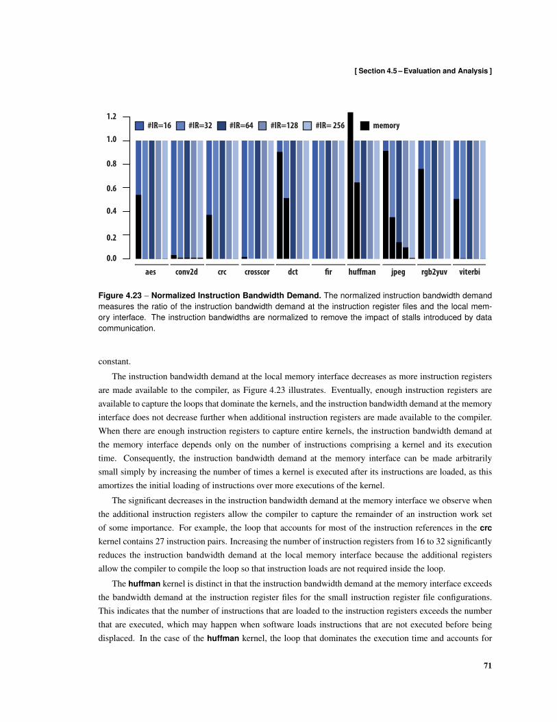
[ Section 4.5 – Evaluation and Analysis ]
#IR=16 #IR=32 #IR=64 #IR=128 #IR= 256 memory
aes conv2d crc crosscor dct !r hu"man jpeg rgb2yuv viterbi0.0
0.4
0.8
1.2
1.0
0.6
0.2
Figure 4.23 – Normalized Instruction Bandwidth Demand. The normalized instruction bandwidth demandmeasures the ratio of the instruction bandwidth demand at the instruction register files and the local mem-ory interface. The instruction bandwidths are normalized to remove the impact of stalls introduced by datacommunication.
constant.
The instruction bandwidth demand at the local memory interface decreases as more instruction registersare made available to the compiler, as Figure 4.23 illustrates. Eventually, enough instruction registers areavailable to capture the loops that dominate the kernels, and the instruction bandwidth demand at the memoryinterface does not decrease further when additional instruction registers are made available to the compiler.When there are enough instruction registers to capture entire kernels, the instruction bandwidth demand atthe memory interface depends only on the number of instructions comprising a kernel and its executiontime. Consequently, the instruction bandwidth demand at the memory interface can be made arbitrarilysmall simply by increasing the number of times a kernel is executed after its instructions are loaded, as thisamortizes the initial loading of instructions over more executions of the kernel.
The significant decreases in the instruction bandwidth demand at the memory interface we observe whenthe additional instruction registers allow the compiler to capture the remainder of an instruction work setof some importance. For example, the loop that accounts for most of the instruction references in the crc
kernel contains 27 instruction pairs. Increasing the number of instruction registers from 16 to 32 significantlyreduces the instruction bandwidth demand at the local memory interface because the additional registersallow the compiler to compile the loop so that instruction loads are not required inside the loop.
The huffman kernel is distinct in that the instruction bandwidth demand at the memory interface exceedsthe bandwidth demand at the instruction register files for the small instruction register file configurations.This indicates that the number of instructions that are loaded to the instruction registers exceeds the numberthat are executed, which may happen when software loads instructions that are not executed before beingdisplaced. In the case of the huffman kernel, the loop that dominates the execution time and accounts for
71
[ Chapter 4 – Instruction Registers ]
the majority of the instruction bandwidth contains several data-dependent control-flow statements withinmultiple nested loops, which introduce regions of code that are executed during some iterations of the loopbut not others. For those regions that contain more than a few instruction pairs, the compiler inserts a shortinstruction sequence after the control-flow statements that precede the regions to load each region as controlenters it. For those regions that contain only a few instruction pairs, the compiler merges each region with theinstruction block that contains the control-flow statement, which is more efficient both in terms of executiontime and instruction bandwidth. In both cases, the compiler loads some instructions that are not executedduring some iterations of the loop; consequently the instruction bandwidth demand at the memory interfaceexceeds the demand at the instruction register file. Increasing the number of instruction registers allowsthe instruction registers to capture entire inner loops, which contain enough instruction reuse to reduce thebandwidth demand at the memory interface below the demand at the instruction registers. Though the jpeg
kernel includes code with similar data-dependent control-flow statements, other parts of the jpeg kernel havesufficient instruction reuse to keep the instruction bandwidth demand at the memory interface below thedemand at the instruction register file.
Comparison To Filter Caches
This section compares the efficiency of instruction registers to filter caches. Figure 4.24 and Figure 4.25show the instruction bandwidth at the memory interface for different direct-mapped and fully-associativefilter cache configurations. The fully-associative filter cache configurations assume a least-recently-usedreplacement policy. The instruction bandwidth demand is calculated as the ratio of the number of instructionsfetched from memory to number of instructions issued. The bandwidth demand reflects the effectiveness ofthe filter caches at filter instruction references.
Two trends are immediately apparent in the instruction bandwidth demand data shown in the figures: theinstruction bandwidth demand decreases as the filter cache capacity increases; and the instruction bandwidthdemand increases as the cache block size increases. The increase in the instruction bandwidth demand weobserve when the cache block size increases deserves some attention because we would generally prefer touse a large cache block size, as increasing the cache block size reduces the number of tags that are requiredto cover the filter cache entries and reduces the memory access time penalty imposed by cache misses. Fig-ure 4.2 illustrates the impact of the cache block size on the number of instructions that must be fetched frommemory and the miss rate.
Increasing the cache block size may introduce additional conflict misses in codes with loops that aresimilar in size to the capacity of the filter cache, as instructions at the start and end of the loop may map tothe same entry when the block size is increased. Typically, this occurs when the loop is not aligned to cacheblock boundaries, which has the effect of reducing the effective capacity of the filter cache. The crc kernelcontains an inner loop that exhibits this problem for the smallest configurations when the cache block sizeincreases from 4 instruction pairs to 8 instruction pairs. The compiler may ameliorate the problem by aligningall loops to cache block boundaries, though this increases the size of the kernel in the backing memory andmay introduce additional capacity misses.
72
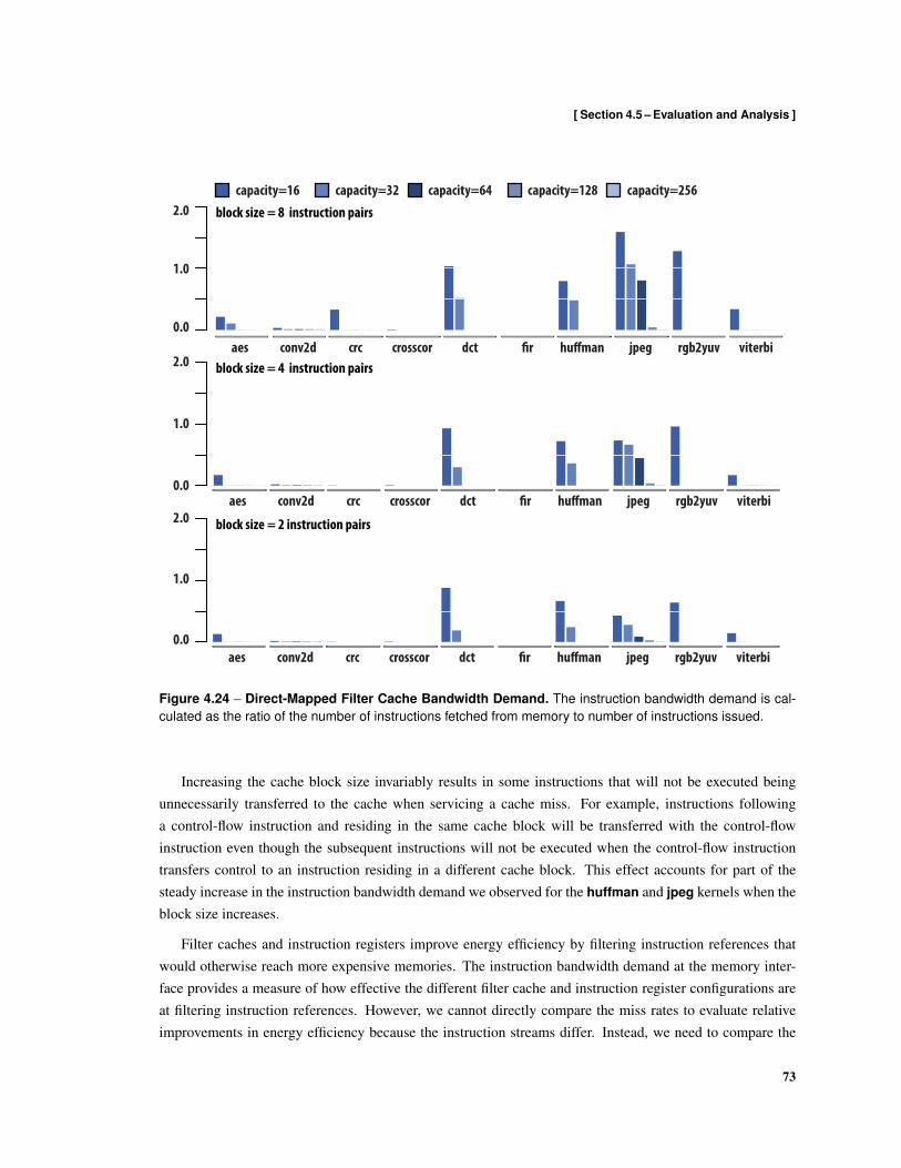
[ Section 4.5 – Evaluation and Analysis ]
0.0
2.0 block size = 2 instruction pairs
block size = 4 instruction pairs
0.0
2.0 block size = 8 instruction pairs
aes conv2d crc crosscor dct !r hu"man jpeg rgb2yuv viterbi
capacity=16 capacity=32 capacity=64 capacity=128 capacity=256
aes conv2d crc crosscor dct !r hu"man jpeg rgb2yuv viterbi
aes conv2d crc crosscor dct !r hu"man jpeg rgb2yuv viterbi
1.0
0.0
2.0
1.0
1.0
Figure 4.24 – Direct-Mapped Filter Cache Bandwidth Demand. The instruction bandwidth demand is cal-culated as the ratio of the number of instructions fetched from memory to number of instructions issued.
Increasing the cache block size invariably results in some instructions that will not be executed beingunnecessarily transferred to the cache when servicing a cache miss. For example, instructions followinga control-flow instruction and residing in the same cache block will be transferred with the control-flowinstruction even though the subsequent instructions will not be executed when the control-flow instructiontransfers control to an instruction residing in a different cache block. This effect accounts for part of thesteady increase in the instruction bandwidth demand we observed for the huffman and jpeg kernels when theblock size increases.
Filter caches and instruction registers improve energy efficiency by filtering instruction references thatwould otherwise reach more expensive memories. The instruction bandwidth demand at the memory inter-face provides a measure of how effective the different filter cache and instruction register configurations areat filtering instruction references. However, we cannot directly compare the miss rates to evaluate relativeimprovements in energy efficiency because the instruction streams differ. Instead, we need to compare the
73

[ Chapter 4 – Instruction Registers ]
0.0
2.0 block size = 2 instruction pairs
0.0
2.0 block size = 4 instruction pairs
0.0
2.0 block size = 8 instruction pairs
aes conv2d crc crosscor dct !r hu"man jpeg rgb2yuv viterbi
aes conv2d crc crosscor dct !r hu"man jpeg rgb2yuv viterbi
aes conv2d crc crosscor dct !r hu"man jpeg rgb2yuv viterbi
1.0
1.0
1.0
capacity=16 capacity=32 capacity=64 capacity=128 capacity=256
Figure 4.25 – Fully-Associative Filter Cache Bandwidth Demand. The instruction bandwidth demand iscalculated as the ratio of the number of instructions fetched from memory to number of instructions issued.The filter cache controller uses a least-recently-used replacement policy.
relative number of instructions fetched from memory, which is shown in Figure 4.26. The filter cache config-urations use a cache block size of 2 instruction pairs, and correspond to the configurations with the smallestinstruction bandwidth demands at the capacities shown.
As the data illustrated in Figure 4.26 demonstrates, the number of instructions fetched from memory istypically a small fraction of the number of instructions executed by most kernels. The notable exception isthe fully-associative filter cache with 32 entries, which performs poorly on the dct kernel. The dct kernelis dominated by an inner loop that contains 38 instruction pairs. The least-recently-used replacement policyresults in the cache controller replacing every instruction stored in the cache during each execution of the loop.Similar adverse interactions between working sets and the replacement policy also explains the behavior ofthe fully-associated filter cache for the huffman and jpeg kernels. For those kernels where the instructionregister configuration fetches more instructions than the direct-mapped filter cache, the preponderance ofthe additional instructions loaded from memory are introduced by the compiler to manage the instruction
74
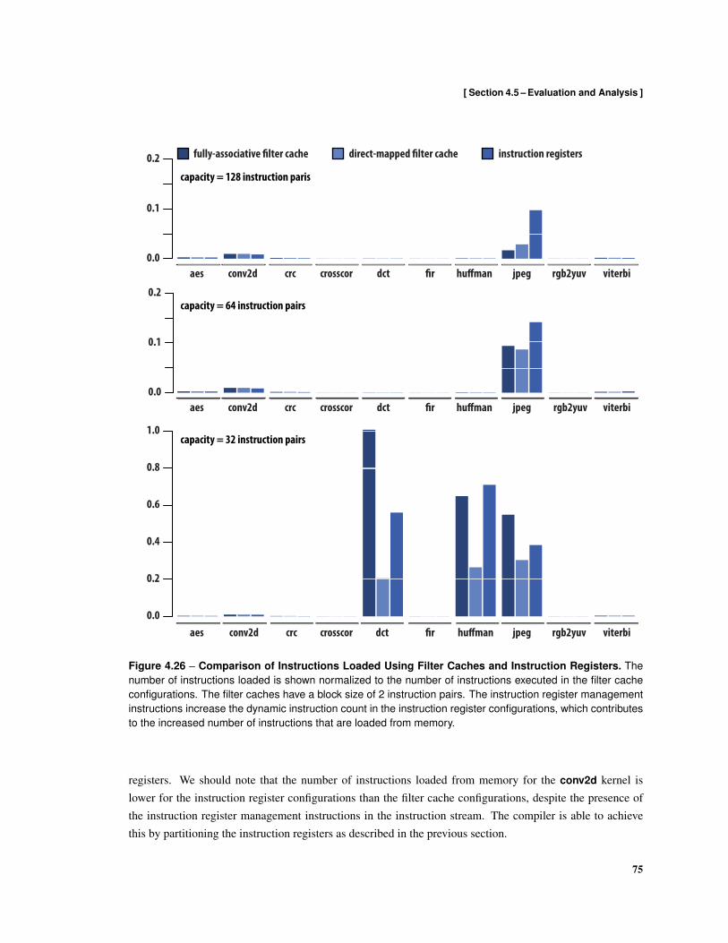
[ Section 4.5 – Evaluation and Analysis ]
aes conv2d crc crosscor dct !r hu"man jpeg rgb2yuv viterbi
aes conv2d crc crosscor dct !r hu"man jpeg rgb2yuv viterbi
0.0
0.2
0.4
0.6
0.8
1.0
aes conv2d crc crosscor dct !r hu"man jpeg rgb2yuv viterbi
fully-associative !lter cache direct-mapped !lter cache instruction registers
capacity = 128 instruction paris
capacity = 64 instruction pairs
capacity = 32 instruction pairs
0.0
0.1
0.2
0.0
0.1
0.2
Figure 4.26 – Comparison of Instructions Loaded Using Filter Caches and Instruction Registers. Thenumber of instructions loaded is shown normalized to the number of instructions executed in the filter cacheconfigurations. The filter caches have a block size of 2 instruction pairs. The instruction register managementinstructions increase the dynamic instruction count in the instruction register configurations, which contributesto the increased number of instructions that are loaded from memory.
registers. We should note that the number of instructions loaded from memory for the conv2d kernel islower for the instruction register configurations than the filter cache configurations, despite the presence ofthe instruction register management instructions in the instruction stream. The compiler is able to achievethis by partitioning the instruction registers as described in the previous section.
75
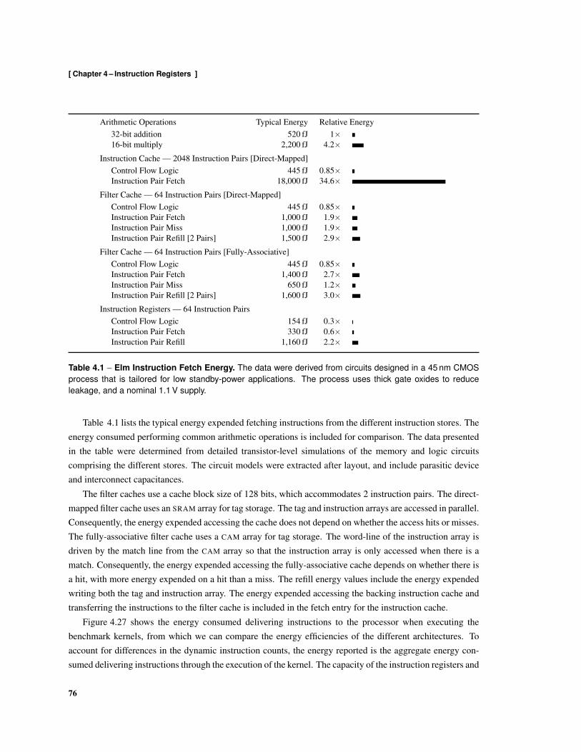
[ Chapter 4 – Instruction Registers ]
Arithmetic Operations Typical Energy Relative Energy32-bit addition 520 fJ 1×16-bit multiply 2,200 fJ 4.2×
Instruction Cache — 2048 Instruction Pairs [Direct-Mapped]Control Flow Logic 445 fJ 0.85×Instruction Pair Fetch 18,000 fJ 34.6×
Filter Cache — 64 Instruction Pairs [Direct-Mapped]Control Flow Logic 445 fJ 0.85×Instruction Pair Fetch 1,000 fJ 1.9×Instruction Pair Miss 1,000 fJ 1.9×Instruction Pair Refill [2 Pairs] 1,500 fJ 2.9×
Filter Cache — 64 Instruction Pairs [Fully-Associative]Control Flow Logic 445 fJ 0.85×Instruction Pair Fetch 1,400 fJ 2.7×Instruction Pair Miss 650 fJ 1.2×Instruction Pair Refill [2 Pairs] 1,600 fJ 3.0×
Instruction Registers — 64 Instruction PairsControl Flow Logic 154 fJ 0.3×Instruction Pair Fetch 330 fJ 0.6×Instruction Pair Refill 1,160 fJ 2.2×
Table 4.1 – Elm Instruction Fetch Energy. The data were derived from circuits designed in a 45 nm CMOSprocess that is tailored for low standby-power applications. The process uses thick gate oxides to reduceleakage, and a nominal 1.1 V supply.
Table 4.1 lists the typical energy expended fetching instructions from the different instruction stores. Theenergy consumed performing common arithmetic operations is included for comparison. The data presentedin the table were determined from detailed transistor-level simulations of the memory and logic circuitscomprising the different stores. The circuit models were extracted after layout, and include parasitic deviceand interconnect capacitances.
The filter caches use a cache block size of 128 bits, which accommodates 2 instruction pairs. The direct-mapped filter cache uses an SRAM array for tag storage. The tag and instruction arrays are accessed in parallel.Consequently, the energy expended accessing the cache does not depend on whether the access hits or misses.The fully-associative filter cache uses a CAM array for tag storage. The word-line of the instruction array isdriven by the match line from the CAM array so that the instruction array is only accessed when there is amatch. Consequently, the energy expended accessing the fully-associative cache depends on whether there isa hit, with more energy expended on a hit than a miss. The refill energy values include the energy expendedwriting both the tag and instruction array. The energy expended accessing the backing instruction cache andtransferring the instructions to the filter cache is included in the fetch entry for the instruction cache.
Figure 4.27 shows the energy consumed delivering instructions to the processor when executing thebenchmark kernels, from which we can compare the energy efficiencies of the different architectures. Toaccount for differences in the dynamic instruction counts, the energy reported is the aggregate energy con-sumed delivering instructions through the execution of the kernel. The capacity of the instruction registers and
76

[ Section 4.5 – Evaluation and Analysis ]
0.0
0.1
0.2
0.3
0.4
aes conv2d crc crosscor dct !r hu"man jpeg rgb2yuv viterbi
control logicinstruction registers
direct-mapped !lter cache
fully-associative !lter cache
backing memoryLegend
Figure 4.27 – Instruction Delivery Energy. The capacity of the instruction registers and filter caches for theconfigurations shown is 64 instruction pairs; the local memory that backs the instruction registers and filtercaches has a capacity of 1024 instruction pairs. The energy shown is normalized to the energy consumed thatwould be consumed delivering instructions directly from the local memory.
filter caches for the configurations shown is 64 instruction pairs; the local memory that backs the instructionregisters and filter caches has a capacity of 1024 instruction pairs.
To illustrate the improvement in energy efficiency the different architectures achieve, the energy shown isnormalized to the energy consumed delivering instructions directly from the local memory.
The control logic component of the energy includes the program counter register, the arithmetic circuitsthat update the program counter and compute branch target addresses, and the control logic and multiplexersthat select the program counter value used to fetch instructions. The instruction register component of theenergy includes the energy expended writing instructions to the instruction registers, reading instructions fromthe instruction registers, and transferring instructions to the data-path. Similarly, the filter cache componentof the energy includes the energy expended reading and writing instructions to the filter caches, readingthe tag entries, and transferring instructions to the data-path. We have not included the energy expended inthe cache controllers required for the filter caches, and consequently the energy reported for the filter cache
77
[ Chapter 4 – Instruction Registers ]
configurations provides a lower bound. The backing memory component of the energy includes the energyexpended reading instructions from the local memory and transferring instructions to the instruction registersor filter caches.
Because the different architectures transfer different numbers of instructions from the backing memory,the relative energy efficiencies of the different architectures is sensitive to the cost of accessing the backingmemory. This may make instruction register organizations appear less efficient, particularly when the instruc-tions that are required to manage the instruction registers contribute to instruction working sets that exceedthe capacity of the instruction registers. Were the amount of energy expended accessing the backing memoryto increase, the instruction register organization would appear less efficient when executing the jpeg kernelbecause it requires that a significant number of instructions be fetched from the backing memory. However,the jpeg kernel can be partitioned into multiple smaller kernels with commensurately smaller working setssimilar to the dct and huffman kernels, which are readily captured in the instruction registers.
4.6 Related Work
Unlike reactive mechanisms such as filter caches [82], software-managed instruction registers reduce instruc-tion movement and avoid the performance penalties caused by high miss rates. Dynamically loaded loopcaches [95], which are loaded on short backwards branches, do not impose miss penalties, but cannot captureloops containing control flow and execute the first two iterations of each loop out of the backing instructioncache while the loop cache is loaded. Pre-loaded loop caches [50] eliminate tag checks when executing in-structions in the loop cache, but cannot be dynamically loaded: they must be large to capture any significantfraction of an application’s instructions and require hardware to detect when instructions should be issuedfrom the loop cache.
The instruction register file proposed by Hines, Whalley, and Tyson [64, 65] provides a form of codecompression in which the most frequently encountered instructions are issued from a small register file aftera packed sequencing instruction is fetched from the instruction cache; the registers cannot be dynamicallyloaded. The tagless instruction cache described by Hines, Whalley, and Tyson [66] uses a clever scheme formodifying a conventional filter cache to exploit situations in which the tag comparison is certain to produce amatch. A common example of an access that is certain to produce a match is fetching consecutive instructionsfrom within the same cache block. This observation is commonly exploited by instruction buffers [29] andcache line buffers [45]. Effectively, the tagless cache is able to operate like an extended line buffer. Thescheme is not truly tagless, as a truncated identifier is used in place of a conventional tag. The scheme requiresa complicated cache controller, and replaces the filter cache tags with auxiliary data that the controller usesto determine whether an instruction is present in the tagless cache. Those configurations that perform bestrequire more auxiliary information than would be required to store the tags used in a conventional filter cache.
The explicit data-flow graph execution model implemented in the TRIPS processor prototype defines ablock-atomic execution model [107] that is similar to earlier block-atomic architectures [103]. The block-atomic execution model implemented in the TRIPS processor executes groups of instructions as atomic units.Instruction groups are fetched, executed, and committed as an atomic unit. Any architectural effects of the
78

[ Section 4.6 – Related Work ]
instructions in an atomic block may be observed by instructions in different atomic instruction blocks onlyafter all of the instruction in the block have been executed and are ready to commit. The compiler mapsinstruction groups into predicated hyperblocks. A hyperblock has a single point of entry and may have mul-tiple points of exit. The execution model does not allow control to transfer within a hyperblock. Encodinginstruction groups as hyperblocks reduces the area and complexity of the branch and branch target predictionhardware implemented in the TRIPS track hyperblocks, as the hardware structures maintain information atthe granularity of hyperblocks rather than individual instructions. The TRIPS processor prototype uses fixedhyperblock size defined by hardware, which results in significant overhead, as the number of instructionsavailable in an instruction group is often insufficient to completely fill a hyperblock. Using large atomic in-struction blocks reduces the cost and complexity of branch prediction. Information used for branch predictionis maintained at the block level rather than the instruction level, so structure with a fixed number of entriesis able to cover more of an application. However, effectiveness of this technique is partially offset by theexpanded code size that results from using a fixed hyperblock size [44].
The vector-thread execution model uses atomic instruction blocks to allow software to encode spatial andtemporal locality in the instruction streams executed by the virtual processors [88]. The virtual processorsexecute RISC-like instructions that are grouped into atomic instruction blocks. An atomic instruction blockhas a single point of entry and may have multiple points of exit. Software specifies the number of instructionscontained in an atomic instruction block. An atomic instruction block may be issued to the virtual processorsby the control processor, or may be explicitly fetched by a virtual processor. An atomic instruction blockmay not contain internal transfers of control, as there is no notion of a program counter or implicit fetchmechanism. Instead, atomic instruction blocks must be explicitly issued by the control processor or fetchedby a virtual processor. Because there is no notion of a program counter, the virtual processors can use ashort instruction pointer to record the position within an atomic instruction block of the next instruction tobe executed. The atomic instruction block abstraction allows the control processor to issue a large number ofinstructions to the virtual processors as a single operation.
The MIT Scale prototype implementation of the vector-thread model distributes atomic instruction blockcaches close to the execution clusters [88]. Distributing the cache memories among the execution clustersallows instructions to be cached close to the function units. Instruction fetch commands specify the addressof the atomic instruction block to be fetched. The specified address is compared against a set of tags todetermine whether the instructions in the atomic instruction block are present in the cache. If there is amiss, an instruction fill unit fetches the atomic instruction block from memory and stores it to the cache.Grouping instructions into atomic instruction blocks allows a single tag comparison to determine whether allof the instructions in the block are present. Though Scale does not allow control to transfer within an atomicinstruction block, instructions may be predicated, or control may conditionally transfer to a different atomicblock. Scale’s vector execution model allows Scale to eliminate many of the control overheads associatedwith executing data-parallel loops, and the vector execution model further reduces the number of instructiontag comparisons that the processor must perform when executing vectorizable codes. However, supportingan execution model in which a large vector of virtual processors are mapped onto a much smaller number ofphysical processors imposes considerable hardware complexity.
79
[ Chapter 4 – Instruction Registers ]
The block-aware instruction set architecture described by Zmily and Kozyrakis uses basic block descrip-tors to describe the block structure of program codes to hardware [157]. This allows the processor front-endto decouple control-flow speculation from the fetching of instructions stored in the instruction cache, whichimproves the performance and energy-efficiency of superscalar processors. The proposed block-aware archi-tecture defines basic block descriptors that software uses to describe the structure of the basic blocks com-prising a program. Descriptors specify information such as the size of a basic block, the type of control-flowinstruction that terminates the basic block, and hints provided by the compiler for predicting the direction ofconditional branches. The basic block descriptors are stored in ancillary structures to decouple control-flowspeculation from the fetching and decoding of instructions from the instruction cache. The descriptors areused to improve the accuracy of instruction prefetching. Because descriptors can be fetched before controltransfers to the basic blocks they describe, the front-end can tolerate longer instruction cache access times.This allows microarchitecture optimizations that improve energy efficiency to be employed in the front-end.For example, the instruction cache can be designed so that the instruction array is accessed after the tagcomparison has been completed to avoid accessing the memory array on a miss.
4.7 Chapter Summary
Instruction registers provide distributed collections of software-managed registers that extend the memoryhierarchy used to deliver instructions to function units. They allow critical instruction working sets suchas loop bodies and computation kernels to be stored close to function units in registers that are inexpensiveto access. Instruction registers are efficiently implemented as distributed collections of small register files.These small register files are fast and inexpensive to access, and distributing them allows instructions to bestored close to function units, reducing the energy consumed transferring instructions to data-path controlpoints.
80
Chapter 5
Operand Registers and Explicit OperandForwarding
This chapter introduces operand registers and explicit operand forwarding, both of which reduce the energyconsumed delivering operands to a processor’s function units. Operand registers and explicit operand for-warding let software capture short-term data reuse and instruction-level producer-consumer data locality ininexpensive registers that are closely integrated with the function units in a processor. Both operand registersand explicit forwarding expose to software the spatial distribution of registers among function units, whichincreases software control over the movement of data between function units and allows software to placedata close to where they will be consumed, reducing the energy expended transporting operands to functionunits. Operand registers and explicit operand forwarding allow the compiler to keep a significant fraction ofthe data bandwidth within the kernels of embedded applications close to the function units, which reducesthe amount of energy expended staging data in registers.
The remainder of this chapter is organized as follows. I begin by introducing the basic concepts motivatingexplicit operand forwarding and operand registers. I then describe how explicit operand forwarding andoperand registers extend a conventional register organization and affect instruction set architecture, usingElm as a specific example of a machine that uses both explicit operand forwarding and operand registers. Ithen discuss microarchitecture, again using Elm as an example of an architecture that implements explicitoperand forwarding and operand registers. After describing the architecture, I discuss compilation issuessuch as instruction scheduling and register allocation. An evaluation follows. I conclude with related workand then summarize the chapter.
5.1 Concepts
Explicit operand forwarding allows software to control the routing of data through the forwarding network sothat ephemeral values can be delivered directly from pipeline registers. This lets software avoid the expenseof storing ephemeral values to register files when ephemeral values can be consumed while they are available
81

[ Chapter 5 – Operand Registers and Explicit Operand Forwarding ]
in the forwarding network.
Operand registers extend a conventional register organization with distributed collections of small, inex-pensive general-purpose operand register files, each of which is integrated with a single function unit in theexecute stage of the pipeline. Essentially, operand registers extend the pipeline registers that deliver operandsto function units in a conventional pipeline into shallow register files; these shallow operand register files re-tain the low access energy of pipeline registers while capturing a greater fraction of operand references. Thislets software capture short-term reuse and instruction-level producer-consumer locality near the functionunits. Both explicit operand forwarding and operand registers increase software control over the movementof operands between function units and register files.
Explicit Operand Forwarding
Explicit operand forwarding lets software control the routing of operands through the forwarding network.Consider the following code fragment.
int x = a + b - c;
During compilation, the compiler translates statements that involve multiple operations into sequence of prim-itive operations, each of which corresponds directly to a machine instructions or a short, fixed-sequence ofmachine instructions. Most compilers would translate the above code fragment into a sequence of operationssimilar to the following.
int t = a + b;
int x = t - c;
The compiler introduces the temporary variable t to forward the result of the addition operation to the sub-traction operation. The corresponding sequence of machine instructions produced by the compiler after per-forming register allocation and instruction selection would be similar to the following sequence of assemblyinstructions, though the register identifiers might differ.
add r5 r2 r3;
sub r1 r5 r4;
When the above sequence of instructions executes, the value of the compiler-introduced temporary t assignedto register r5 is delivered by the forwarding network. Register r5 is unnecessarily written when the instruc-tions execute. Register r5 simply provides an identifier that allows the logic that controls the forwardingnetwork to detect that the result of the add instruction must be forwarded to the sub instruction. Writing theresult of the addition to the register file consumes more energy than performing the addition. For example,performing a 32-bit addition in a 45 nm low-power CMOS technology consumes about 0.52 pJ; writing theresult of the addition to a 32-entry register file consumes about 1.45 pJ. Furthermore, using register r5 toforward the intermediate value unnecessarily increases register pressure, as whatever value was previously inregister r5 is lost after the add instruction completes.
82

[ Section 5.1 – Concepts ]
Explicit operand forwarding lets software orchestrate the routing of operands through the forwardingnetwork so that ephemeral values need not be written to register files. Instead, ephemeral values can beconsumed while they are available in the forwarding network. Explicit operand forwarding introduces theconcept of forwarding registers to provide an explicit architectural name for the result of the last instructionthat a function unit executed. Forwarding registers establish architectural names for the physical pipelineregisters residing at the end of the execute (EX) stage. Software can use forwarding registers as operands toexplicitly forward the result of a previous instruction. Similarly, software can use a forwarding register as adestination to direct the result of an instruction to a forwarding register, which indicates that the result shouldnot be written to the register file. For example, the following sequence of assembly instructions forwardsthe result of the add operation through forwarding register t0, which is the forwarding register name for thepipeline register that captures the output of the ALU.
add t0 r2 r3;
sub r1 t0 r4;
Forwarding register t0 appears in two different contexts: it appears as the destination of the add instructionto specify that the result of the addition does not need to be stored in the register file, and it appears asan operand to the sub instruction to specify that the fist operand of the subtraction operation is the resultproduced by the previous instruction.
Operand Registers
Registers provide low-latency and high-bandwidth locations for storing temporary and intermediate values,and for staging data transfers between memory and function units. Registers are usually implemented asmulti-ported register files, which are denser and faster than latches and flip-flops, though not as dense asSRAM. Most of the architectural registers that are significant to software are implemented as registers inregister files. Some registers that are accessed every cycle, such as the program counter, or are accessedirregularly, such as status registers that are accessed through special instructions, are implemented indepen-dently as dedicated registers.
Accessing data stored in registers is considerably less expensive than accessing data stored in memory,both in terms of execution time and energy. Consequently, optimizing compilers spend considerable effortallocating registers in order to limit the number of expensive memory accesses that are performed. Increasingthe number of registers that are available to software allows more data to be stored in registers rather thanmemory, reducing the number of memory references. Similarly, increasing the number of registers thatare exposed to the compiler allows larger working sets to be captured in registers, reducing the number ofvariables that must be spilled to memory when register demand exceeds register availability. In general, theability of the register file to filter references depends on its capacity relative to the working sets present inan application. However, providing more registers requires additional register file capacity. Because largerregister files are more expensive to access, the cost of accessing data stored in registers tends to increaseas more registers are made available. Ignoring the complexity of encoding larger register specifiers in afixed-length instruction word, there is a fundamental tension between the benefits and costs of increasing the
83
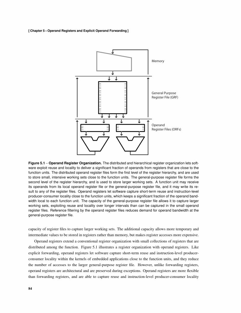
[ Chapter 5 – Operand Registers and Explicit Operand Forwarding ]
Operand Register Files (ORFs)
General PurposeRegister File (GRF)
Memory
Figure 5.1 – Operand Register Organization. The distributed and hierarchical register organization lets soft-ware exploit reuse and locality to deliver a significant fraction of operands from registers that are close to thefunction units. The distributed operand register files form the first level of the register hierarchy, and are usedto store small, intensive working sets close to the function units. The general-purpose register file forms thesecond level of the register hierarchy, and is used to store larger working sets. A function unit may receiveits operands from its local operand register file or the general-purpose register file, and it may write its re-sult to any of the register files. Operand registers let software capture short-term reuse and instruction-levelproducer-consumer locality close to the function units, which keeps a significant fraction of the operand band-width local to each function unit. The capacity of the general-purpose register file allows it to capture largerworking sets, exploiting reuse and locality over longer intervals than can be captured in the small operandregister files. Reference filtering by the operand register files reduces demand for operand bandwidth at thegeneral-purpose register file.
capacity of register files to capture larger working sets. The additional capacity allows more temporary andintermediate values to be stored in registers rather than memory, but makes register accesses more expensive.
Operand registers extend a conventional register organization with small collections of registers that aredistributed among the function. Figure 5.1 illustrates a register organization with operand registers. Likeexplicit forwarding, operand registers let software capture short-term reuse and instruction-level producer-consumer locality within the kernels of embedded applications close to the function units, and they reducethe number of accesses to the larger general-purpose register file. However, unlike forwarding registers,operand registers are architectural and are preserved during exceptions. Operand registers are more flexiblethan forwarding registers, and are able to capture reuse and instruction-level producer-consumer locality
84
[ Section 5.2 – Microarchitecture ]
within longer instruction sequences. This allows operand registers to capture a greater fraction of operandbandwidth and to offer more relaxed instruction scheduling constraints.
Like explicit operand forwarding, operand registers exploit short-term reuse and locality to reduce de-mand for operand bandwidth at the general-purpose register. The operand registers effectively filter datareferences closer to the function units than the general-purpose registers. This keeps more communicationlocal to the function units and improves energy efficiency: the small operand register files are inexpensiveto access, and the expense of traversing the forwarding network and pipeline register preceding the execute(EX) stage of the pipeline is avoided. For example, delivering two operands from a general-purpose registerfile and writing back the result consumes 3.1 pJ, which exceeds the 2.2 pJ consumed by a 16-bit multiplica-tion; using operand registers to stage the operands and the result consumes only 0.78 pJ, which is close to the0.52 pJ consumed by a 32-bit addition.
5.2 Microarchitecture
Forwarding registers establish architectural names for the physical pipeline registers residing at the end of theexecute (EX) stage. Forwarding registers retain the result of the last instruction that wrote the execute (EX)pipeline register. To preserve the registers, data-path control logic clock-gates the pipeline registers duringinterlocks and when nops execute. This allows operands to be explicitly forwarded between instructionsthat execute multiple cycles apart when intervening instructions do not update the physical registers used tocommunicate the operands [142].
The value returned from the local memory when a load instruction executes cannot be explicitly forwardedbecause load values do not traverse the pipeline registers at the end of the execute (EX) stage; instead,architectural registers retime load values arriving from memory.
Processors with deeper pipelines generally need more registers to cover longer operation latencies. Ex-plicit forwarding can be extended for deeper pipelines by establishing additional explicit names for the resultsof recently executed instructions that are available within the forwarding network. However, the pipeline reg-isters that stage the forwarded operands are not conventional architectural registers and may be difficult topreserve when interrupts and exceptions occur. When interrupts are a concern, the compiler can be directedto disallow the explicit forwarding of operands between instructions that may cause exceptions.
Operand Registers
Operand registers are implemented as very small register files that are integrated with the function units inthe execute stage of the pipeline. This allows operand registers to provide the energy efficiency of explicitforwarding while preserving the behavior of general-purpose registers. Accessing the operand register filesin the execute (EX) stage may contribute to longer critical path delays. However, the operand register readoccurs in parallel with the activation of the forwarding network, and much of the operand register file accesstime is covered by the forwarding of operands from the write-back (WB) stage. Regardless, register organi-zations using operand registers require fast, and consequently small, operand register files to avoid creating
85
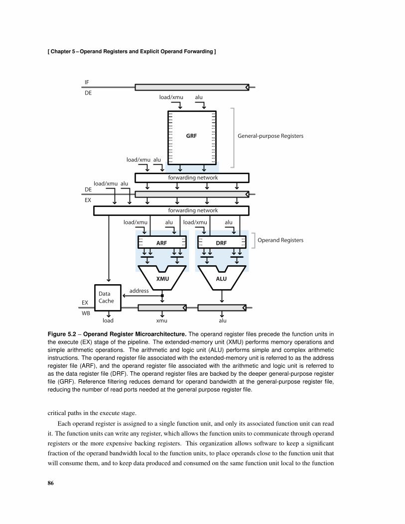
[ Chapter 5 – Operand Registers and Explicit Operand Forwarding ]
Operand Registers
General-purpose Registers
DataCache
address
WB
EX
load/xmu alu
forwarding network
aluload/xmu
forwarding network
EX
DE
load/xmu alu
load/xmu alu
load/xmu alu
load aluxmu
DE
IF
ARF DRF
ALUXMU
GRF
Figure 5.2 – Operand Register Microarchitecture. The operand register files precede the function units inthe execute (EX) stage of the pipeline. The extended-memory unit (XMU) performs memory operations andsimple arithmetic operations. The arithmetic and logic unit (ALU) performs simple and complex arithmeticinstructions. The operand register file associated with the extended-memory unit is referred to as the addressregister file (ARF), and the operand register file associated with the arithmetic and logic unit is referred toas the data register file (DRF). The operand register files are backed by the deeper general-purpose registerfile (GRF). Reference filtering reduces demand for operand bandwidth at the general-purpose register file,reducing the number of read ports needed at the general purpose register file.
critical paths in the execute stage.
Each operand register is assigned to a single function unit, and only its associated function unit can readit. The function units can write any register, which allows the function units to communicate through operandregisters or the more expensive backing registers. This organization allows software to keep a significantfraction of the operand bandwidth local to the function units, to place operands close to the function unit thatwill consume them, and to keep data produced and consumed on the same function unit local to the function
86

[ Section 5.3 – Example ]
Arithmetic Operations Relative Energy32-bit addition 520 fJ 1×16-bit multiply 2,200 fJ 4.2×
General-Purpose Register File — 32 words (4R+2W)32-bit read 830 fJ 1.6×32-bit write back 1,450fJ 2.8×
General-Purpose Register File — 32 words (2R+2W)32-bit read 800 fJ 1.5×32-bit write back 1,380 fJ 2.7×
Operand Register File — 4 words (2R+2W)32-bit read 120 fJ 0.2×32-bit write back 540 fJ 1.0×
Forwarding Register — 1 word (1R+1W)32-bit forward 530 fJ 1.0×
Data Cache — 2K words (1R+1W) [8-way set-associative with CAM tags]32-bit load 10,100 fJ 19.4×32-bit store 14,900 fJ 28.6×
Table 5.1 – Energy Consumed by Common Operations. The data were derived from circuits implementedin a 45 nm CMOS process that is tailored for low standby-power applications. The process uses thick gateoxides to reduce leakage, and a nominal supply of 1.1 V to provide adequate drive current.
unit. Furthermore, reference filtering by the operand registers reduces demand for operand bandwidth fromthe shared general-purpose registers, which allows the number of read ports to the general-purpose registerfile to be reduced without adversely impacting performance. This makes the general-purpose register filesmaller and shortens its bit-lines, reducing its access costs by decreasing the bit-line capacitance switchedduring read and write operations. It also reduces the cost of updating a register because fewer access devicescontribute to the capacitance internal to each register.
5.3 Example
Consider the following code fragment, which computes the product of the complex values a and b and assignsthe product to x. The operands are 16-bit fixed-point integers.
100 x.re = a.re * b.re - a.im * b.im;
101 x.im = a.re * b.im + a.im * b.re;
Table 5.1 lists typical amounts of energy expended performing the arithmetic operations, memory operations,and register file accesses performed in the example code. The register file read energy includes the cost oftransferring an operand from the register file to an input of a function unit. The register file write energyincludes the cost of transferring a result from the output of a function unit to the register file.
Figure 5.3 shows the sequence of operations generated by the compiler, and Figure 5.4 shows the corre-sponding sequence of assembly instructions for a conventional register organization. The assembly listingassumes that the address of variable a resides in register r10, the address of b resides in r11, and the address
87
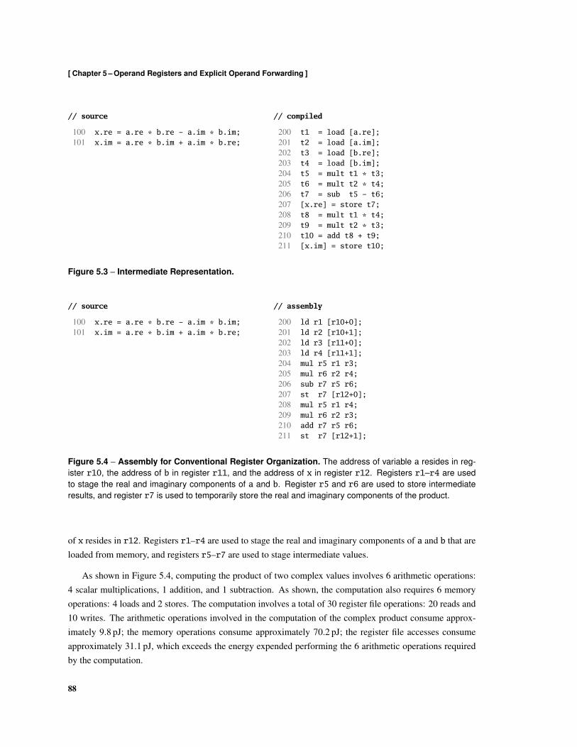
[ Chapter 5 – Operand Registers and Explicit Operand Forwarding ]
// source
100 x.re = a.re * b.re - a.im * b.im;101 x.im = a.re * b.im + a.im * b.re;
// compiled
200 t1 = load [a.re];201 t2 = load [a.im];202 t3 = load [b.re];203 t4 = load [b.im];204 t5 = mult t1 * t3;205 t6 = mult t2 * t4;206 t7 = sub t5 - t6;207 [x.re] = store t7;208 t8 = mult t1 * t4;209 t9 = mult t2 * t3;210 t10 = add t8 + t9;211 [x.im] = store t10;
Figure 5.3 – Intermediate Representation.
// source
100 x.re = a.re * b.re - a.im * b.im;101 x.im = a.re * b.im + a.im * b.re;
// assembly
200 ld r1 [r10+0];201 ld r2 [r10+1];202 ld r3 [r11+0];203 ld r4 [r11+1];204 mul r5 r1 r3;205 mul r6 r2 r4;206 sub r7 r5 r6;207 st r7 [r12+0];208 mul r5 r1 r4;209 mul r6 r2 r3;210 add r7 r5 r6;211 st r7 [r12+1];
Figure 5.4 – Assembly for Conventional Register Organization. The address of variable a resides in reg-ister r10, the address of b in register r11, and the address of x in register r12. Registers r1–r4 are usedto stage the real and imaginary components of a and b. Register r5 and r6 are used to store intermediateresults, and register r7 is used to temporarily store the real and imaginary components of the product.
of x resides in r12. Registers r1–r4 are used to stage the real and imaginary components of a and b that areloaded from memory, and registers r5–r7 are used to stage intermediate values.
As shown in Figure 5.4, computing the product of two complex values involves 6 arithmetic operations:4 scalar multiplications, 1 addition, and 1 subtraction. As shown, the computation also requires 6 memoryoperations: 4 loads and 2 stores. The computation involves a total of 30 register file operations: 20 reads and10 writes. The arithmetic operations involved in the computation of the complex product consume approx-imately 9.8 pJ; the memory operations consume approximately 70.2 pJ; the register file accesses consumeapproximately 31.1 pJ, which exceeds the energy expended performing the 6 arithmetic operations requiredby the computation.
88
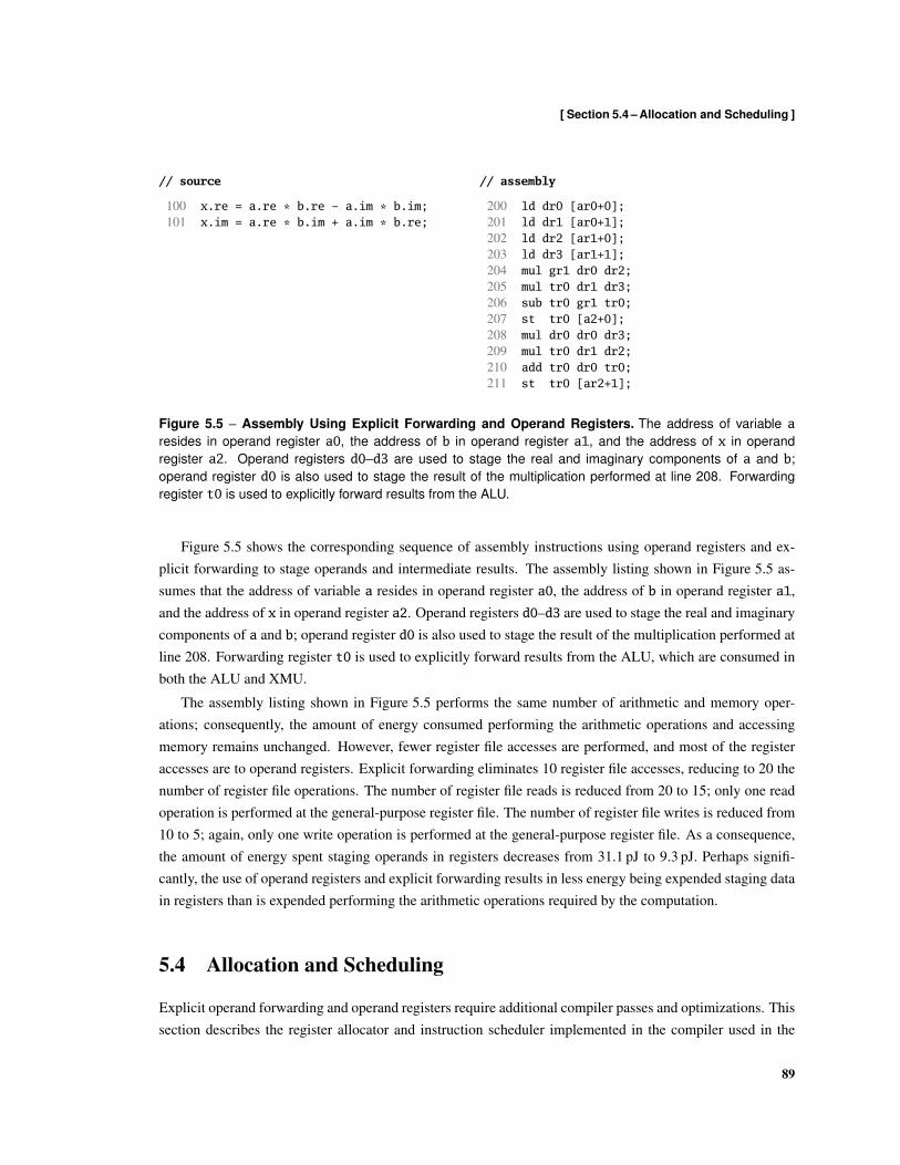
[ Section 5.4 – Allocation and Scheduling ]
// source
100 x.re = a.re * b.re - a.im * b.im;101 x.im = a.re * b.im + a.im * b.re;
// assembly
200 ld dr0 [ar0+0];201 ld dr1 [ar0+1];202 ld dr2 [ar1+0];203 ld dr3 [ar1+1];204 mul gr1 dr0 dr2;205 mul tr0 dr1 dr3;206 sub tr0 gr1 tr0;207 st tr0 [a2+0];208 mul dr0 dr0 dr3;209 mul tr0 dr1 dr2;210 add tr0 dr0 tr0;211 st tr0 [ar2+1];
Figure 5.5 – Assembly Using Explicit Forwarding and Operand Registers. The address of variable aresides in operand register a0, the address of b in operand register a1, and the address of x in operandregister a2. Operand registers d0–d3 are used to stage the real and imaginary components of a and b;operand register d0 is also used to stage the result of the multiplication performed at line 208. Forwardingregister t0 is used to explicitly forward results from the ALU.
Figure 5.5 shows the corresponding sequence of assembly instructions using operand registers and ex-plicit forwarding to stage operands and intermediate results. The assembly listing shown in Figure 5.5 as-sumes that the address of variable a resides in operand register a0, the address of b in operand register a1,and the address of x in operand register a2. Operand registers d0–d3 are used to stage the real and imaginarycomponents of a and b; operand register d0 is also used to stage the result of the multiplication performed atline 208. Forwarding register t0 is used to explicitly forward results from the ALU, which are consumed inboth the ALU and XMU.
The assembly listing shown in Figure 5.5 performs the same number of arithmetic and memory oper-ations; consequently, the amount of energy consumed performing the arithmetic operations and accessingmemory remains unchanged. However, fewer register file accesses are performed, and most of the registeraccesses are to operand registers. Explicit forwarding eliminates 10 register file accesses, reducing to 20 thenumber of register file operations. The number of register file reads is reduced from 20 to 15; only one readoperation is performed at the general-purpose register file. The number of register file writes is reduced from10 to 5; again, only one write operation is performed at the general-purpose register file. As a consequence,the amount of energy spent staging operands in registers decreases from 31.1 pJ to 9.3 pJ. Perhaps signifi-cantly, the use of operand registers and explicit forwarding results in less energy being expended staging datain registers than is expended performing the arithmetic operations required by the computation.
5.4 Allocation and Scheduling
Explicit operand forwarding and operand registers require additional compiler passes and optimizations. Thissection describes the register allocator and instruction scheduler implemented in the compiler used in the
89

[ Chapter 5 – Operand Registers and Explicit Operand Forwarding ]
evaluation, and addresses compilation issues associated with allocating registers and scheduling instructionsfor a processor that provides operand registers and supports explicit operand forwarding.
Scheduling for Explicit Forwarding
A basic explicit operand forwarding compiler pass can be implemented as a peephole optimization per-formed after instruction scheduling and register allocation. The peephole optimization identifies instructionsequences in which the result produced by an instruction in the sequence can be explicitly forwarded to aninstruction that appears later in the sequence and replaces the operand of the later instruction with a forward-ing register. In general, the optimization pass cannot replace the destination of the producing instruction witha forwarding register unless it determines that all consumers of the result can receive the result from the for-warding register. Essentially, the optimization pass must know the locations of all uses of the result, and thatall uses have been updated to use the forwarding register before modifying the producing instruction. Thisrequires information about the definitions and uses of the result of the producing instruction that is generatedby data-flow analysis such as reaching definitions analysis which may not be available during a peepholeoptimization pass.
In general, an explicit forwarding optimization pass is more effective when performed between instruc-tion scheduling and register allocation. This allows the register allocator to avoid allocating registers tothose variables that can be explicitly forwarded. Typically, variables that can be explicitly forwarded arealso ideal candidates for operand registers and will displace other variables competing for operand registers;consequently, performing an explicit forwarding pass before register allocation allows more variables to beassigned to operand registers and achieves better operand register utilization.
The optimization pass implemented in the evaluation compiler is performed immediately before registerallocation, which occurs after instruction scheduling. The optimization pass identifies instructions whoseresults are consumed before another instruction executes on the same function unit. If all uses of the variabledefined by an instruction appear before another instruction executes on the same function unit, the optimiza-tion pass assigns the variable to the forwarding register. Those variables that are assigned to the forwardingregisters are ignored during register allocation.
The instruction scheduler can expose opportunities for explicit forwarding by scheduling dependent in-structions so that the result of the earlier instruction will be available in the forwarding register when the laterinstruction reaches the execute stage of the pipeline. To improve locality, the compiler schedules sets of de-pendent instructions, and attempts to schedule sequences of dependent instructions on the same function unit.This exposes opportunities for the compiler to explicitly forward operands, and to store those that cannot beexplicitly forwarded in local operand registers.
Allocating Operand Registers
Operand registers could be allocated using a conventional register allocator provided that it accounts for therestricted connectivity between the operand register files and function units. Any variables that are operandsto instructions that execute on different function units must be assigned to general-purpose registers. Variables
90

[ Section 5.4 – Allocation and Scheduling ]
that are read by only one function unit could be allocated to the operand registers associated with the functionunit. The register allocator could assign each variable to the least expensive register that is available forthe variable. However, without considering the broader impact of which variables are assigned to operandregisters energy efficiency, we should not expect such a register allocator to select the best variables foroperand registers.
The register allocator used in the compiler sorts the variables before assigning registers so that variablesthat are better candidates for operand registers are assigned registers before variables that are less suitablecandidates. After sorting the variables, the compiler scans the sorted list and assigns the least expensiveregister available when it reaches that variable. The compiler preferentially schedules dependent instructionson the same function unit in an attempt to expose opportunities for using the local operand registers to stageintermediates between dependent instructions.
The register allocation phase proceeds as follows. The register allocator first constructs an interferencegraph for all of the variables in the compilation unit. The nodes in the interference graph represent variablesin the compilation unit, and the edges in the interference graph indicate that the live ranges of the two nodesconnected by the edge overlap. Two variables cannot be assigned to the same register if the correspondingnodes in the interference graph are connected by an edge. After constructing the initial interference graph, theregister allocator coalesces pairs of nodes that correspond to the source and destination of a copy operation.Both variables represented by a coalesced node will be assigned to the same register, which usually allowsone or more move operation to be eliminated.
After coalescing nodes in the interference graph, the register allocator analyzes the compilation unit todetermine the order in which variables should be assigned to registers. This phase of the register allocationprocess produces a sorted list of all of the nodes in the interference graph. Two strategies for ordering thenodes in the sorted list are described in the following sections.
Finally, the register allocator scans the sorted list and assigns registers to the nodes in the interferencegraph. The allocator assigns the least expensive register available for the node. The allocator uses the inter-ference graph to determine which registers are available. Basically, a register cannot be assigned a registerthat has already been assigned to an adjacent node in the interference graph. For example, the register alloca-tor will assign a data register to a node representing variables that are only read by the ALU if a data registeris available when the allocator encounters the node; otherwise, the allocator will assign a general-purposeregister to the node. After selecting a register, the register allocator colors the node in the interference graphwith the assigned register.
Should the register allocator encounter a variable that cannot be assigned a register because there areno registers available, it terminates and requests the instruction schedule be modified to spill the variable tomemory. The spill instruction, which stores the spilled value to memory, is inserted immediately after thevalue is produced so that a forwarding register can be used to forward the value, thereby avoiding the needto allocate a register for the spilled variable until it is used. The register allocation process is repeatedlyattempted until it completes successfully.
91
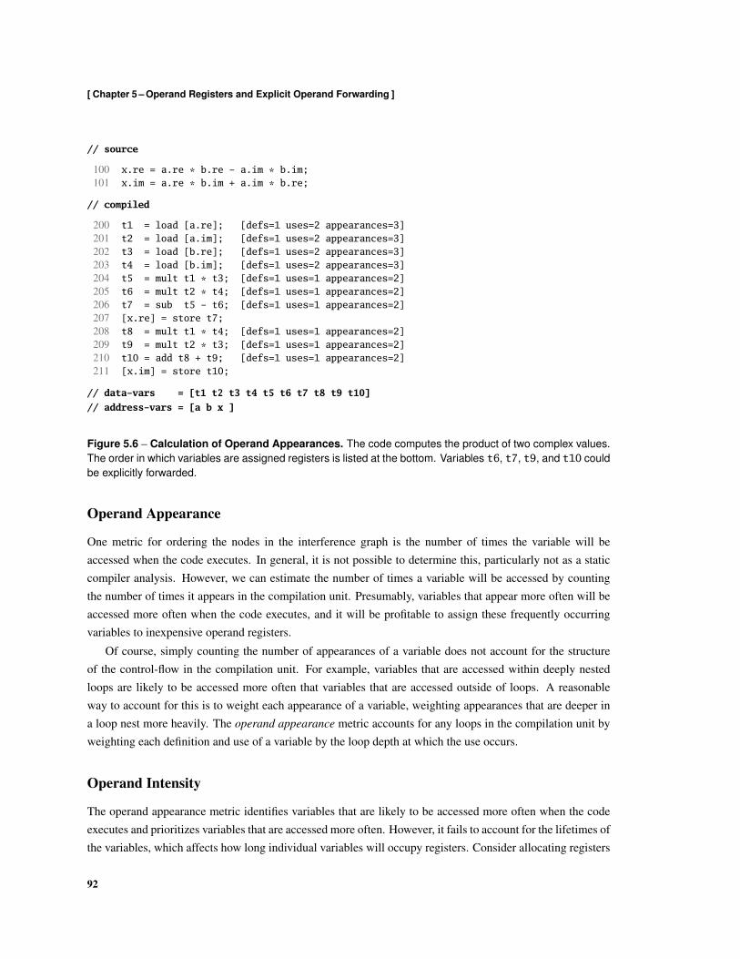
[ Chapter 5 – Operand Registers and Explicit Operand Forwarding ]
// source
100 x.re = a.re * b.re - a.im * b.im;101 x.im = a.re * b.im + a.im * b.re;
// compiled
200 t1 = load [a.re]; [defs=1 uses=2 appearances=3]201 t2 = load [a.im]; [defs=1 uses=2 appearances=3]202 t3 = load [b.re]; [defs=1 uses=2 appearances=3]203 t4 = load [b.im]; [defs=1 uses=2 appearances=3]204 t5 = mult t1 * t3; [defs=1 uses=1 appearances=2]205 t6 = mult t2 * t4; [defs=1 uses=1 appearances=2]206 t7 = sub t5 - t6; [defs=1 uses=1 appearances=2]207 [x.re] = store t7;208 t8 = mult t1 * t4; [defs=1 uses=1 appearances=2]209 t9 = mult t2 * t3; [defs=1 uses=1 appearances=2]210 t10 = add t8 + t9; [defs=1 uses=1 appearances=2]211 [x.im] = store t10;
// data-vars = [t1 t2 t3 t4 t5 t6 t7 t8 t9 t10]
// address-vars = [a b x ]
Figure 5.6 – Calculation of Operand Appearances. The code computes the product of two complex values.The order in which variables are assigned registers is listed at the bottom. Variables t6, t7, t9, and t10 couldbe explicitly forwarded.
Operand Appearance
One metric for ordering the nodes in the interference graph is the number of times the variable will beaccessed when the code executes. In general, it is not possible to determine this, particularly not as a staticcompiler analysis. However, we can estimate the number of times a variable will be accessed by countingthe number of times it appears in the compilation unit. Presumably, variables that appear more often will beaccessed more often when the code executes, and it will be profitable to assign these frequently occurringvariables to inexpensive operand registers.
Of course, simply counting the number of appearances of a variable does not account for the structureof the control-flow in the compilation unit. For example, variables that are accessed within deeply nestedloops are likely to be accessed more often that variables that are accessed outside of loops. A reasonableway to account for this is to weight each appearance of a variable, weighting appearances that are deeper ina loop nest more heavily. The operand appearance metric accounts for any loops in the compilation unit byweighting each definition and use of a variable by the loop depth at which the use occurs.
Operand Intensity
The operand appearance metric identifies variables that are likely to be accessed more often when the codeexecutes and prioritizes variables that are accessed more often. However, it fails to account for the lifetimes ofthe variables, which affects how long individual variables will occupy registers. Consider allocating registers
92

[ Section 5.5 – Allocation and Scheduling ]
// source
100 x.re = a.re * b.re - a.im * b.im;101 x.im = a.re * b.im + a.im * b.re;
// compiled
200 t1 = load [a.re]; [defs=1 uses=2 life=8 intensity=0.38]201 t2 = load [a.im]; [defs=1 uses=2 life=8 intensity=0.38]202 t3 = load [b.re]; [defs=1 uses=2 life=7 intensity=0.43]203 t4 = load [b.im]; [defs=1 uses=2 life=5 intensity=0.60]204 t5 = mult t1 * t3; [defs=1 uses=1 life=2 intensity=1.00]205 t6 = mult t2 * t4; [defs=1 uses=1 life=1 intensity=2.00]206 t7 = sub t5 - t6; [defs=1 uses=1 life=1 intensity=2.00]207 [x.re] = store t7;208 t8 = mult t1 * t4; [defs=1 uses=1 life=2 intensity=1.00]209 t9 = mult t2 * t3; [defs=1 uses=1 life=1 intensity=2.00]210 t10 = add t8 + t9; [defs=1 uses=1 life=1 intensity=2.00]211 [x.im] = store t10;
// data-vars = [t10 t9 t7 t6 t8 t5 t4 t3 t2 t1]
// address-vars = [a b x ]
Figure 5.7 – Calculation of Operand Intensity. The code computes the product of two complex values. Theorder in which variables are assigned registers is listed at the bottom. Data register candidates t10, t9, t7,and t6, which are prioritized because they have the greatest operand intensity, could be explicitly forwarded
for variables in the code shown in Figure 5.6, which has been annotated with the operand appearances metriccomputed for each variable where it is defined. Let us assume that the target machine has a single operandregister and does not support explicit forwarding. A register allocator using the operand appearance metricwould allocate one of t1 – t4 to the operand register, as these variables have the greatest operand appearancevalues. To make the example concrete, let us assume that t1 is assigned to the operand register and occupiesthe register from line 201 through 208. The operand register is used 3 times between 201 and 208. Theoperand register would have been more productively employed if instead the register allocator had assignedthe operand register to variables t5, t7, and t8, as it would be used 6 times between line 201 and 208.
Intuitively, the operand bandwidth captured in operand registers can be increased by allocating operandregisters to variables that are either short-lived or are long-lived and frequently accessed. The intuition hereis that short-lived variables will not occupy an operand register for very long, so it will be available for useby other variables. The register allocator can identify variables that exhibit these properties by computinga measure of operand intensity for each variable. Operand intensity is computed by dividing the operandappearance value for a variable by its estimated lifetime. The lifetime is estimated statically as the numberof instructions for which the variable is live, as computed by a conventional live-variables data-flow analysis.The lifetime estimate does not account for the loop structure. This is intentional. The primary purpose ofincluding the estimated lifetimes of variables is used to order appearances at the same level of loop nesting.An example of the computation appears in Figure 5.7.
93

[ Chapter 5 – Operand Registers and Explicit Operand Forwarding ]
5.5 Evaluation
Figure 5.8 shows the normalized operand bandwidth at the register files and memory interface for several em-bedded kernels. The figure shows the composition of the operand read bandwidth and the result write band-width as additional operand registers are made available to the compiler. Pairs of adjacent columns illustratethe impact of explicit forwarding: the left column shows bandwidth composition with explicit forwarding,and the right column shows the composition without explicit forwarding. The dedicated accumulator regis-ters, which are used by multiply-and-accumulate operations, are integrated with the ALU and are reported asoperand registers. The accumulators appear in all of the configurations, and contribute to the operand registerbandwidth reported for the configuration that lacks operand register files. The configuration with 8 operandregisters, which associates 4 operand registers with the ALU and 4 with the XMU, corresponds to the Elmregister organization. To illustrate the impact of operand register organization, the read and write bandwidthsare normalized to a conventional register organization with a unified register file with 4 read ports and 2 writeports. The data shown in the figures were collected using a general-purpose register file with 2 read ports and2 write ports. The reduction in the read port bandwidth available at the general-purpose register file can resultin additional register accesses, as some shared data may be duplicated; it also may increase kernel executiontimes, as additional cycles may be required to resolve read port conflicts. The data is normalized to correctfor additional register accesses.
The number of general-purpose registers remains constant at 32 register for all configurations. The addi-tional operand registers increase the aggregate number of registers that are available to the compiler, whichallows the compiler to reduce the number of variables that are spilled to memory. Both the dct and huffman
kernels show a reduction in aggregate operand bandwidth because there are fewer register spills, which intro-duce load and store operations, both of which read registers. The jpeg kernel shows a reduction for the samereason, and includes code similar to the dct and huffman kernels. However, the aggregate benefit that canbe attributed simply to the additional registers is modest, as the compiler introduces few register spills evenwhen there are no operand registers.
Figure 5.8 shows that operand registers are an effective organization for capturing a significant fractionof operand bandwidth local to the function units. Without explicit forwarding, the configuration with 8operand registers, which provides four operand registers per function unit, captures between 32% and 66%of all operand bandwidth in operand registers; the operand registers account for 43% to 87% of all registerreferences. As the figure illustrates, explicit operand forwarding replaces operand register references withexplicit operand forwards. With explicit operand forwarding, the configuration with 8 operand registerscaptures between 25% and 64% of all operand bandwidth in operand registers; the operand registers accountfor 38% to 81% of all register references.
In addition to capturing instruction-level producer-consumer data locality within the function units, ex-plicit operand forwarding reduces register pressure. The crc and crosscor kernels clearly illustrate the ef-fectiveness of explicit operand forwarding at reducing operand register pressure when the number of operandregisters is limited; the configurations that use explicit operand forwarding are able to capture a greater frac-tion of data references in operand registers.
94

[ Section 5.5 – Evaluation ]
aes
conv2d
crc
crosscor
dct
!r
hu"man
jpeg
rgb2yuv
0.0
1.0
viterbi
hardware forward operand register general-purpose register memory
0.0
1.0
0.0
1.0
0.0
1.0
0.0
1.0
0.0
1.0
0.0
1.0
0.0
1.0
0.0
1.0
0.0
1.0
explicit forward
0 2 4 6 8 10 12
0 2 4 6 8 10 12
0 2 4 6 8 10 12
0 2 4 6 8 10 12
0 2 4 6 8 10 12 0 2 4 6 8 10 12
0 2 4 6 8 10 12
0 2 4 6 8 10 12
0 2 4 6 8 10 12
0 2 4 6 8 10 12
Figure 5.8 – Impact of Operand Registers on Data Bandwidth. The number of operand registers appearson the horizontal axis. Pairs of adjacent columns illustrate the impact of explicit forwarding: the left columnshows bandwidth composition with explicit forwarding, and the right column shows the composition withoutexplicit forwarding.
95
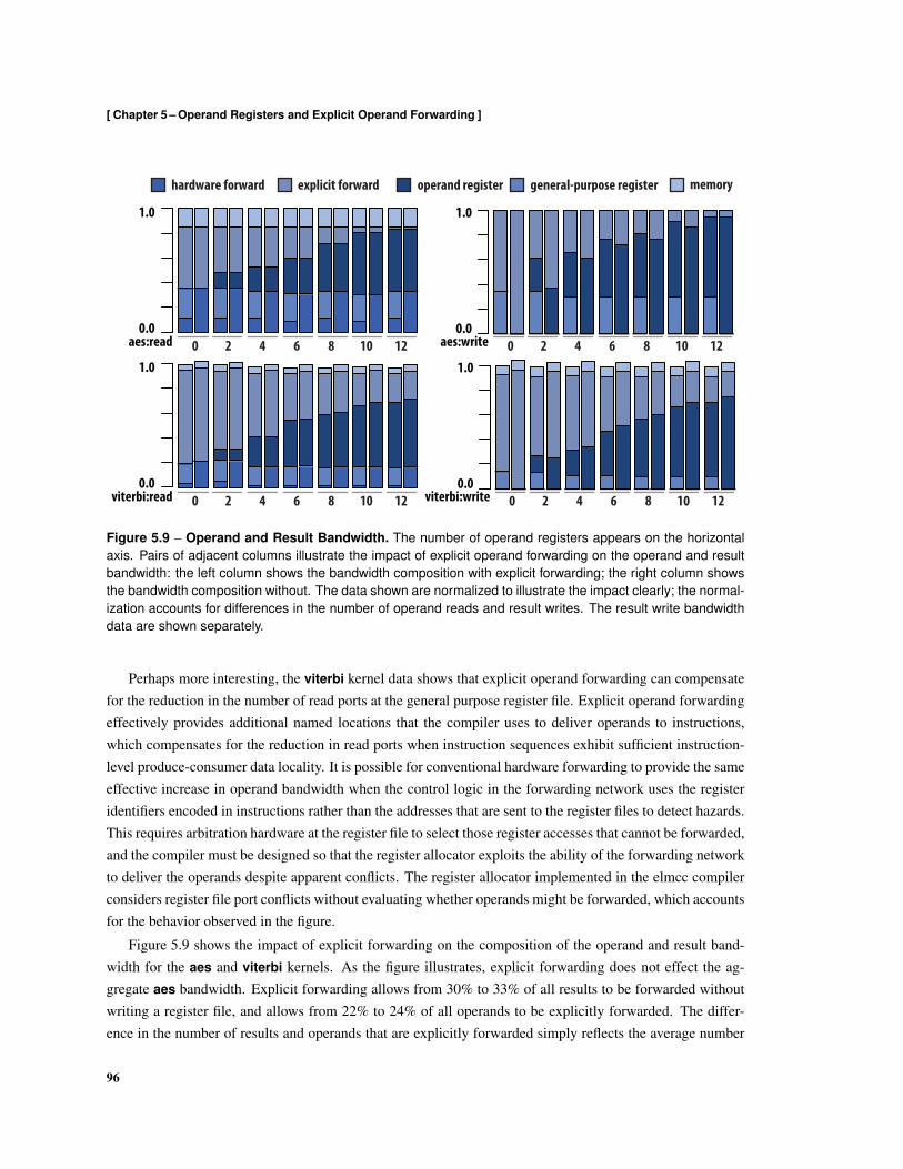
[ Chapter 5 – Operand Registers and Explicit Operand Forwarding ]
aes:write
hardware forward operand register general-purpose register memory
0.0
1.0
explicit forward
0 2 4 6 8 10 12aes:read0.0
1.0
0 2 4 6 8 10 12
viterbi:read viterbi:write0.0
1.0
0.0
1.0
0 2 4 6 8 10 12 0 2 4 6 8 10 12
Figure 5.9 – Operand and Result Bandwidth. The number of operand registers appears on the horizontalaxis. Pairs of adjacent columns illustrate the impact of explicit operand forwarding on the operand and resultbandwidth: the left column shows the bandwidth composition with explicit forwarding; the right column showsthe bandwidth composition without. The data shown are normalized to illustrate the impact clearly; the normal-ization accounts for differences in the number of operand reads and result writes. The result write bandwidthdata are shown separately.
Perhaps more interesting, the viterbi kernel data shows that explicit operand forwarding can compensatefor the reduction in the number of read ports at the general purpose register file. Explicit operand forwardingeffectively provides additional named locations that the compiler uses to deliver operands to instructions,which compensates for the reduction in read ports when instruction sequences exhibit sufficient instruction-level produce-consumer data locality. It is possible for conventional hardware forwarding to provide the sameeffective increase in operand bandwidth when the control logic in the forwarding network uses the registeridentifiers encoded in instructions rather than the addresses that are sent to the register files to detect hazards.This requires arbitration hardware at the register file to select those register accesses that cannot be forwarded,and the compiler must be designed so that the register allocator exploits the ability of the forwarding networkto deliver the operands despite apparent conflicts. The register allocator implemented in the elmcc compilerconsiders register file port conflicts without evaluating whether operands might be forwarded, which accountsfor the behavior observed in the figure.
Figure 5.9 shows the impact of explicit forwarding on the composition of the operand and result band-width for the aes and viterbi kernels. As the figure illustrates, explicit forwarding does not effect the ag-gregate aes bandwidth. Explicit forwarding allows from 30% to 33% of all results to be forwarded withoutwriting a register file, and allows from 22% to 24% of all operands to be explicitly forwarded. The differ-ence in the number of results and operands that are explicitly forwarded simply reflects the average number
96

[ Section 5.5 – Evaluation ]
of operands to an instruction exceeding the average number of result values. Explicit forwarding reducesoperand register pressure, and allows more data bandwidth to be captured close to the function units. Thisis apparent from the impact explicit operand forwarding has on the aes write bandwidth, which shows thatexplicit forwarding directs more of the result bandwidth to registers that are integrated with the function units.The number of register file reads is not affected because the pipeline control logic detects that an operand willbe forwarded and suppresses unnecessary register file accesses.
The viterbi kernel exhibits a reduction in aggregate data bandwidth when the compiler uses explicitoperand forwarding. The reduction results from the compiler eliminating operand and general-purpose reg-ister accesses that communicate operands across multiple instruction pairs. Essentially, the compiler uses thetemporary registers to explicitly communicate data between instructions that execute multiple cycles apart.When ephemeral data is explicitly forwarded, a register write and subsequent read are eliminated, whichreduces the aggregate data bandwidth and keeps more of the data bandwidth local to the function units.
Energy Efficiency
Figure 5.10 shows the energy expended delivering data to function units. To illustrate the impact of the reg-ister organization and explicit operand forwarding, the data has been normalized within each kernel. Theconfiguration with no operand registers uses a general-purpose register file with 4 read ports; the other con-figurations use a general-purpose register file with 2 read ports. Because the register file is physically smallerand the internal cell capacitances are reduced, less energy is expended accessing the register file with 2 readports. However, to avoid conflating the reduction in the general-purpose register file access energy, we haveused the 4 port register file access energy for all of the configurations. We have also assumed that the localmemory that backs the register files is a 2 kB direct-mapped cache rather than the software-managed En-semble memory used in Elm. This reflects a more conventional processor organization, but makes memoryaccesses more expensive. Consequently, the data presented in the figure provides a conservative estimate ofthe energy efficiency improvements achieved from the operand register organization.
As the figure clearly illustrates, operand registers and explicit operand forwarding both reduce the energyexpended delivering data to function units. Operand registers alone reduce the energy consumed staging datatransfers to function units by 19% to 32% for configuration with 4 operand registers per function unit; theyreduce the energy consumed in the registers files and forwarding network by 31% to 56%. Combined, operandregisters and explicit forwarding reduce the energy consumed staging data transfers to function units by 19%to 38% for the configuration with 4 operand registers per function unit; they reduce the energy consumed inthe registers files and forwarding network by 35% to 57%.
Operand registers effectively filter accesses to more expensive registers. Increasing the number of operandregisters allows the operand registers to filter more accesses. As Figure 5.10 shows, this improves energyefficiency by reducing the energy consumed accessing the general-purpose register file. As we provisionadditional operand registers, the amount of energy expended accessing operand registers increases. In part,this is because operand registers are accessed more often. Additionally, the larger operand register filesare more expensive to access, and the efficiency advantage offered by small register files diminishes as we
97
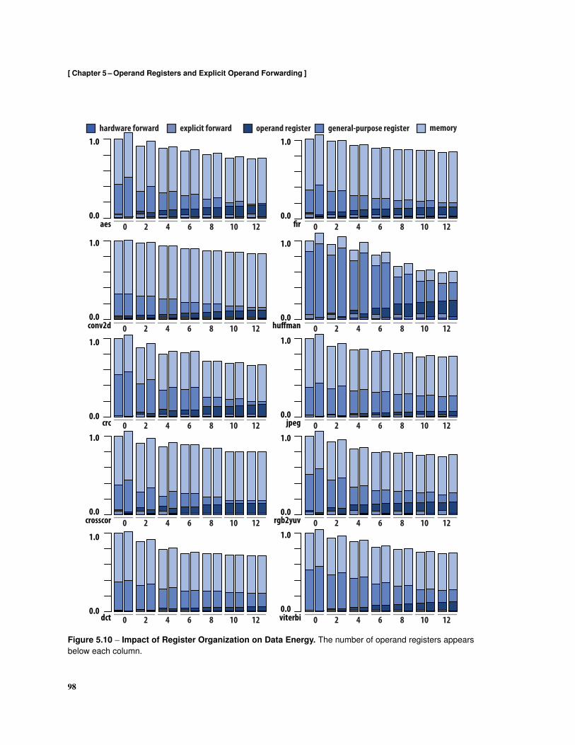
[ Chapter 5 – Operand Registers and Explicit Operand Forwarding ]
aes
conv2d
crc
crosscor
dct
!r
hu"man
jpeg
rgb2yuv
0.0
1.0
viterbi
hardware forward operand register general-purpose register memory
0.0
1.0
0.0
1.0
0.0
1.0
0.0
1.0
0.0
1.0
0.0
1.0
0.0
1.0
0.0
1.0
0.0
1.0
explicit forward
0 2 4 6 8 10 12
0 2 4 6 8 10 12
0 2 4 6 8 10 12
0 2 4 6 8 10 12
0 2 4 6 8 10 12 0 2 4 6 8 10 12
0 2 4 6 8 10 12
0 2 4 6 8 10 12
0 2 4 6 8 10 12
0 2 4 6 8 10 12
Figure 5.10 – Impact of Register Organization on Data Energy. The number of operand registers appearsbelow each column.
98
[ Section 5.5 – Evaluation ]
introduce additional operand registers. To compensate, one could segment the bit-lines within the operandregister files to allow some operand registers to be accessed less expensively. However, we have found that thecapacity of the operand register files is typically limited by area efficiency considerations rather than energyefficiency considerations: operand register files must be small enough to provide sufficiently fast access timesto avoid introducing critical paths that will limit the frequency at which the processor will operate at.
As should be evident from contrasting the data presented for the different kernels, data working sets have asignificant impact on the effectiveness of operand registers and explicit forwarding. Consider the breakdownof operand bandwidth for the aes and rgb2yuv kernels shown in Figure 5.8, and what we can infer about theworking sets of the two kernels from the data. The slow increase in operand register bandwidth in aes asthe number of operand registers increases reflects the lack of small working sets with significant short-termlocality and reuse for the compiler to promote to operand registers. Conversely, the significant fraction of theoperand bandwidth in rgb2yuv captured with few operand registers reflects the compiler promoting a criticalset of high-intensity variables to operand registers. Four data and four address registers are sufficient tocapture the critical working set of rgb2yuv, and further increasing the number of operand registers results inlittle additional bandwidth capture, as only low-intensity variables are promoted to operand registers. Despitecontributing a small fraction of all data references, memory accesses are considerably more expensive thanregister file accesses and are responsible for the preponderance of the data access energy.
Compilers and Explicit Operand Forwarding
With operand registers and explicit operand forwarding providing detailed control over the movement ofdata throughout the pipeline, it is reasonable to ponder whether we could rely exclusively on the compiler toforward all operands explicitly. This would eliminate the need for dedicated hardware to detect dependenciesbetween instructions within the processor pipeline. The significant disadvantage of removing the hardwarethat detects dependencies and automatically forwards operands is that it tends to increase the number ofinstructions comprising kernels. The compiler may need to schedule explicit idle cycles to ensure the resultshave reached their destination register before a dependent instruction reads the register. We have found thisto be particularly problematic near points where control-flow converges, as the compiler must conservativelyschedule instructions to ensure that all dependencies are satisfied regardless of where control arrives from.Another issue is that the compiler must use operand registers to transfer results to dependent instructionswhen a region lacks sufficient instruction-level parallelism to hide both pipeline and function unit operationlatencies; variables that are assigned to operand registers for this reason may otherwise be inferior candidates.
Figure 5.11 shows the impact of relying exclusively on the compiler to forward operands. Pairs of adja-cent columns show the benefit of hardware detecting read-after-write hazards and managing the forwardingnetwork: the left column shows the execution time when the pipeline control logic detects hazards and for-wards operands as necessary; the right column shows the execution time when the compiler must detect haz-ards and explicitly forward operands when possible. The number of operands registers appears below eachcolumn. The operand registers are distributed evenly between the ALU and XMU. All of the configurationshave a general-purpose register file with 2 read ports and 2 write ports.
99
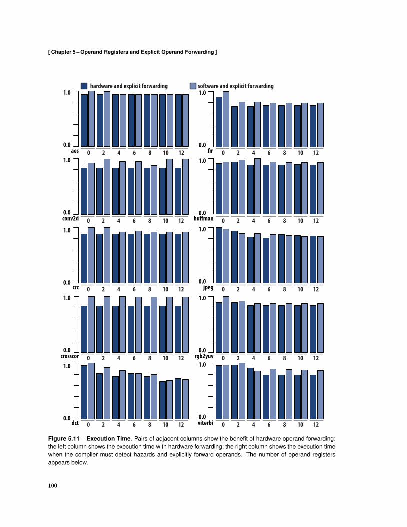
[ Chapter 5 – Operand Registers and Explicit Operand Forwarding ]
aes
conv2d
crc
crosscor
dct
!r
hu"man
jpeg
rgb2yuv
0.0
1.0
viterbi
hardware and explicit forwarding
0.0
1.0
0.0
1.0
0.0
1.0
0.0
1.0
0.0
1.0
0.0
1.0
0.0
1.0
0.0
1.0
0.0
1.0
software and explicit forwarding
0 2 4 6 8 10 12
0 2 4 6 8 10 12
0 2 4 6 8 10 12
0 2 4 6 8 10 12
0 2 4 6 8 10 12 0 2 4 6 8 10 12
0 2 4 6 8 10 12
0 2 4 6 8 10 12
0 2 4 6 8 10 12
0 2 4 6 8 10 12
Figure 5.11 – Execution Time. Pairs of adjacent columns show the benefit of hardware operand forwarding:the left column shows the execution time with hardware forwarding; the right column shows the execution timewhen the compiler must detect hazards and explicitly forward operands. The number of operand registersappears below.
100
[ Section 5.6 – Evaluation ]
Because the execution time reported is for compiled kernels, the execution times exhibit some artifactsthat are introduced by the heuristics used in the register allocation and instruction scheduling phases of thecompiler. These artifacts appear as an increase in the number of operand registers producing a small increasein the execution time. Typically, this results when the compiler assigns a variable that is an operand toinstructions that execute in different function units to an operand register and is unable to schedule a copyoperation without introducing an additional cycle to the instruction schedule.
Increasing the number of operand registers allows the operand register files to capture more data refer-ences, which reduces the demand for operand bandwidth at the general-purpose register file. The reductionin the execution times we observe when the number of operand registers increases results primarily from areduction in the number of port conflicts at the general-purpose register file. The notable exception is the dct
kernel. The additional register capacity allows more of the data working set to be captured in registers, whichreduces the number of the memory operations that are executed. The compiler used to compile the kernelsdoes not exploit the ability of the forwarding network to deliver more than 2 operands in the decode stage,which effectively allows more than 2 operands to be provided at the general-purpose register file when someare forwarded. Instead, the compiler conservatively assumes that an instruction pair may contain at most 2operands that reside in general-purpose registers. This results a perceptible performance degradation for the8 operand register configuration of the dct kernel.
As Figure 5.11 shows, the performance of kernels may degrade significantly when we rely exclusivelyon the compiler to forward operands. For example, the throughput of the crosscor kernel decreases by 16%.The energy expended in the instruction register files exceeds the modest savings realized by eliminating thehardware that is implemented to detect dependencies. Other kernels, notably the aes and crc kernels, performreasonably well when we rely exclusively on the compiler provided that we provision a sufficient number ofoperand registers to capture the short-term instruction-level dependencies within the performance-criticalregions of the code.
Technology and Design Considerations
Explicit forwarding and operand registers provide greater benefits when VLSI technology and design con-straints limit the efficiency of multi-ported register files and memories. For example, often memory com-pilers are optimized for large memories and are not designed to generate efficient small memories. Withoutaccess to efficient small memories and register files, the cost of staging operands in general-purpose registersincreases, which improves the relative efficiencies provided by operand registers and explicit forwarding.Similarly, standard cell libraries rarely allow wide multiplexers to be implemented as efficiently as is pos-sible when a datapath is constructed using custom design and layout techniques, which may increase thecost of implementing the multiplexers that are needed to read operand registers, making explicit forwardingcomparatively more attractive.
101
[ Chapter 5 – Operand Registers and Explicit Operand Forwarding ]
5.6 Related Work
Distributed [122], clustered [40], banked [30], and hierarchical [154] register organizations improve accesstimes and densities by partitioning registers across multiple register files and reducing the number of readand write ports to each register file. The number of ports needed to deliver a certain operand bandwidthcan be reduced by using SIM register organizations [116] to allow each port to deliver or receive multipleoperands to multiple function units. Such SIMD register organizations are suitable for the subset of dataparallel applications that are readily vectorized, but impose inefficiencies when data and control dependenciesprevent data parallel computations from being vectorized.
The hierarchical CRAY-1 register organization [123] associates dedicated scalar and address registerswith groups of scalar and address function units and provides dedicated backing register files to filter spillsto memory. In contrast, operand register files are significantly smaller, optimized for access energy, and eachis integrated with a single function unit in the execute stage of the pipeline to reduce the cost of transferringoperands between an operand register file and its dedicated function unit. This allows operand registers toachieve greater reductions in energy consumption in processors with short operation latencies and workloadswith critical working sets and short-term producer-consumer locality that can be captured in a small numberof registers. Operand registers further differ by allowing both levels of the register hierarchy to be directlyaccessed. This avoids the overhead of executing instructions to explicitly move data between the backing reg-ister files and those that deliver operands to the function units [154]. It also avoids the overhead of replicatingdata in multiple register files [30].
Horizontally microcoded machines such as the FPS-164 [142] required that software explicitly route allresults and operands between function units and register files. This work introduces opportunistic explicitsoftware forwarding into a conventional pipeline, where automatic forwarding performed by the forwardingcontrol logic avoids the increase in code size and dynamic instruction counts needed to explicitly route alldata.
Hampton described a processor architecture that exposes pipeline registers to software[57] and allows theresult of an instruction to be directed to a pipeline register. Like explicit bypass registers, this exposed archi-tecture allowed software to replace some writes to a register file with writes to pipeline registers. Hamptonreports similar data on the number of register file writes that can be eliminated. The architecture is limited inthat a result could be written to at most one pipeline register, so only operands that are accessed by a singleinstruction could be communicated explicitly through the exposed pipeline registers. Operands with multipleconsumers must be assigned to general purpose registers. The architecture relied on software restart markersto recover from exceptions that might alter the state of the pipeline registers [58].
5.7 Chapter Summary
Operand register files are small, inexpensive register files that are integrated in the execute stage of thepipeline; explicit operand forwarding lets software opportunistically orchestrate the routing of operandsthrough the forwarding network to avoid writing ephemeral values to registers. Both operand registers and
102

[ Section 5.7 – Chapter Summary ]
explicit operand forwarding let software capture short-term reuse and locality in inexpensive registers that areintegrated with the function units. This keeps a significant fraction of operand bandwidth local to the functionunits, and reduces the energy consumed communicating data through registers and the forwarding networks.
103
Chapter 6
Indexed and Address-Stream Registers
This chapter introduces the concepts of indexed registers and address-stream registers, and describe an ar-chitecture that uses indexed registers and address-stream registers to expose hardware for performing vectormemory operations to software.
6.1 Concepts
Registers are used to store intermediate values and to stage data transfers between function units and memory.In an architecture such as Elm that provides operand registers, general-purpose registers are used to captureworking sets that exhibit medium-term reuse and locality. Providing additional general-purpose registers al-lows software to capture larger working sets in registers, reducing the amount of data that must be transferredbetween registers and memory. This improves energy efficiency and performance, as registers are less ex-pensive and faster to access than memory. However, exposing additional architectural registers to softwarerequires the use of instruction encodings that dedicate more bits for encoding register names. This leavesfewer bits available for encoding operations or increases the number of bits required to encode an instruction,neither of which are desirable.
Perhaps more significantly, many compute-intensive kernels, and particularly those with enough struc-tured reuse to benefit from large register files, access data in ways that makes it difficult to exploit largeregister files without using software techniques, such as loop unrolling, to expose additional scalar variablesthat can be assigned to registers. A kernel that operates on the elements of an array serves to illustrate thispoint. Before assigning the elements of the array to registers, the compiler must typically replace each refer-ence to an element of the array with an equivalent reference to a scalar variable that is introduced explicitlyfor this purpose, a transformation commonly referred to as scalar replacement. If a kernel accesses the arrayin a loop using an index that is a non-trivial affine function of the loop induction variable, the loop must beunrolled to enable the scalar replacement transformation. Because loop unrolling replicates operations withinthe bodies of loops, loop unrolling increases the number of instructions in the critical instruction working setsand kernels of an application. Reductions in the energy consumed staging operands in registers may be offset
104

[ Section 6.1 – Concepts ]
by increases in the energy consumed loading instructions from memory. Consequently, software techniquessuch as loop unrolling that exploit additional registers but introduce additional instructions are unattractivefor architectures such as Elm because the additional instructions increase instruction register pressure.
Before continuing, we should observe that the aggregate number of general-purpose registers that maybe accessed by the instructions residing in the instruction registers will be limited to a small multiple ofthe number of instruction registers. This follows from each instruction being able to reference at most 3general-purpose registers, though many instructions will reference fewer. There are techniques for allowingsoftware to access a larger number of physical registers. For example, vector processors are able to providea large number of physical registers and offer compact instruction encodings by associating a large numberof physical registers with a single vector register identifier. Similarly, architectures that provide registerwindows allow software to access different sets of physical registers by rotating through distinct windows,though these are typically used to avoid saving and restoring registers at function call boundaries, and whenentering and terminating interrupt and trap handlers [114].
Index registers let software access some subset of the architectural registers indirectly. The registers thatcan be accessed indirectly through the index registers are referred to as indexed registers. Some of the indexedregisters may be architectural registers that can be accessed using a conventional register name; others maybe dedicated indexed registers that can only be accessed through index registers. Index and indexed registersimprove efficiency by allowing larger data working sets to be efficiently stored in the register hierarchy; theylet software increase the fraction of intra-kernel data locality that can be compactly captured in registerswithout resorting to software techniques such as loop unrolling that increase the instruction working set ofa kernel. Thus, index and indexed registers simultaneously address the problem of allowing a processorto increase the number of registers that are available to software without requiring instruction set changesand the problem of allowing software to exploit addition registers without resorting to techniques such asloop unrolling that increases the number of instructions in the working sets of the important kernels withinembedded applications. Like vector registers, index and indexed establish an association between a largenumber of physical registers and a register identifier that is exposed to software. However, index and indexedare more general and more flexible: index and indexed registers expose the association to software and letsoftware control the assignment of physical registers to register identifiers, and allow the physical registers tobe accessed using multiple register identifiers.
Vector memory operations transfer multiple data words between memory and the indexed registers, whichimproves code density by allowing a single vector memory instruction to encode multiple memory opera-tions. Techniques that improve code density improve efficiency in general, and are particularly attractivefor architectures such as Elm that achieve efficiency in part by delivering a significant fraction of instructionbandwidth from a small set of inexpensive instruction registers. Vector memory operations provide a meansfor software to explicitly encode spatial locality within the operation, which allows hardware to improve thescheduling and handling of the memory operations. Decoupling allows the memory operations that transferthe elements of a vector to complete while the processor continues to execute instructions, which lets soft-ware schedule computation in parallel with memory operations. Decoupling vector memory operations alsoassists software in tolerating memory access latencies, as vector memory operations can be initiated early to
105

[ Chapter 6 – Indexed and Address-Stream Registers ]
allow the operations more time to complete.
The Elm architecture exposes the hardware that generates sequences of addresses for vector memory op-erations as address-stream registers. The address-stream registers deliver sequences of addresses and offsetsthat can be combined with other registers to compute the effective addresses of memory operations. Softwarecontrols the address sequences computed by the address-stream registers by loading configuration words frommemory. Software can save the state of an address sequence by storing the address-stream register to mem-ory, and can later restore the sequence by loading the register from memory. This lets software map multipleaddress sequences onto the address-stream registers. Software can move elements from the address sequencesto other registers, which allows software to implement complex address calculations using a combination ofaddress-stream registers and general-purpose and address registers.
Exposing the address generators as address-stream registers allows software to use the hardware to accel-erate repetitive address calculations, improving both performance and efficiency by eliminating instructionsthat perform explicit address computations from the instruction stream. It also simplifies the task of decom-posing a large transfer that can be compactly expressed using vector memory operations and address-streamregisters into a sequence of smaller operations that better exploit the storage available in the register organi-zation: the address-stream registers maintain the state of the operation between transfers.
6.2 Microarchitecture
Figure 6.1 illustrates where index, indexed, and address-stream registers reside in the register organization.The index and indexed registers reside with the general-purpose registers and are read early in the pipeline.The address-stream registers are located with the XMU in the execute stage of the pipeline, where theyeffectively extend the address register file. The following sections describe microarchitectural considerationsand the implementation of indexed and address-stream registers in the Elm.
Index and Indexed Registers
The instruction set architecture allows the index registers to be implemented as an extension of the general-purpose registers. The Elm instruction set architecture allows a processor to implement between 32 and 2048indexed registers, and defines indexed registers xr0 though xr31 to be aliases of general-purpose registers gr0through gr31. Consequently, index registers xr0 through xr31 may use the same physical memory as is usedto implement the general-purpose registers. Any additional indexed registers that a processor implementsrequire dedicated memory.
When the number of indexed registers exceeds the number of general-purpose registers by a small factor,the indexed registers and general-purpose registers can be implemented efficiently as a single unified registerfile. Though any additional capacity required for the indexed registers increases the cost of accessing general-purpose registers, a unified register organization improves area efficiency by avoiding the duplication of manyof the peripheral circuits found in a register file.
106

[ Section 6.2 – Microarchitecture ]
Operand Registers
General-purpose Registers
Memoryaddress
WB
EX
load/xmu aluforwarding network
aluload/xmu
forwarding network
EX
DE
load/xmu alu
load/xmu alu
load/xmu alu
load aluxmu
DE
IF
ARF DRF
ALUXMU
GRF
XRF
ASFAddress-stream Registers
XRMUupdate
IndexRegisters
load/xmu
IndexedRegisters
Figure 6.1 – Index Registers and Address-stream Registers. Index registers allow registers in the general-purpose register file to be accessed indirectly through the index registers. The index registers reside in theindex register file (XRF). The index register management unit (XRMU) implements logic for automaticallyupdating pointers stored in the index registers after each reference. Address-stream registers extend theaddress registers integrated with the XMU, and are used to automate the generation of fixed sequences ofaddresses. Hardware associated with the address-stream registers automatically updates the value storedin an address-stream register after each reference. The address-stream registers are implemented in theaddress-stream register file (ASF).
107
[ Chapter 6 – Indexed and Address-Stream Registers ]
When the number of indexed registers greatly exceeds the number of general-purpose registers, the ad-ditional physical registers may be implemented as a dedicated register file to avoid increasing the cost ofaccessing the general-purpose registers. This register organization offers the advantage of provisioning ad-dition register file ports. A unified register organization limits the number of operands that can be deliveredfrom the general-purpose registers and indexed registers. The partitioned register file organization allows 2operands to be delivered from general-purpose registers and 2 operands to be delivered from indexed reg-isters. Perhaps more significantly, it provides an additional 2 write ports, allowing data from the memoryinterface to be returned to the indexed registers while the XMU writes results back to the general-purposeregisters.
Forwarding
Elm automatically forwards values that are stored to indexed registers. Because an index register and ageneral-purpose register identifier may refer to the same physical register, index register identifiers cannotbe used to detect when it is necessary to forward a result. Essentially, the possibility of aliases, introducedby indirection, prevents the pipeline control logic from inspecting the index register identifiers encoded ininstructions to detect data dependencies. Fortunately, this alias problem is easily solved. The key insightin forwarding indexed registers is that the physical addresses of the indexed register, not the index registeridentifiers encoded in instructions, should be used to detect dependencies. Accordingly, the pipeline controllogic implemented in Elm uses the physical addresses of any indexed registers to detect when data should beforwarded. Similarly, the pipeline interlocks also use physical register addresses to detect data hazards that theforwarding network cannot resolve. Even if different register files were used for general-purpose registers andindexed registers, it would still be necessary for the pipeline control logic to use physical register addressesto detect dependencies because the sets of indexed registers accessed through different index registers maynot be disjoint, and consequently multiple index registers may refer to the same indexed register.
Source indexed register addresses are determined when the index registers are accessed in the decodestage, and advance along with operands read from the indexed register through the pipeline. Destinationindexed register addresses are determined in the execute stage of the pipeline. The destination indexed registeraddresses are used to forward results that are destined for indexed registers when the results are sent to theindexed register file in the write-back stage. Though the destination addresses could be determined in thewrite-back stage, the time required to access the index registers would contribute to the delay associated withforwarding operands through the forwarding network, and would adversely impact the frequency at which theprocessor could operate. Once the addresses of the destination and source indexed registers are available, theforwarding hardware simply forwards indexed registers as though they were general-purpose registers, usingthe indexed register addresses to determine where results should be sent through the forwarding network.
Interlocks
The processor must ensure that an operation that modifies an index register appears to complete before sub-sequent operations that use the index register to access the indexed registers are initiated. The forwarding
108
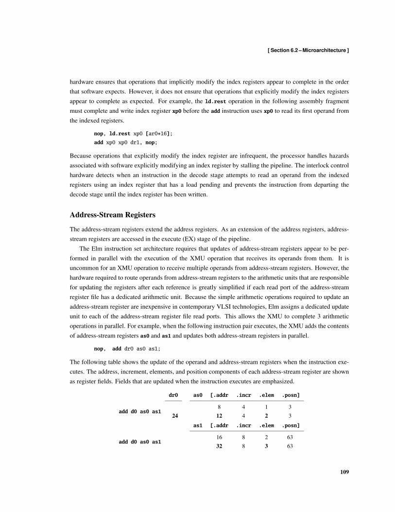
[ Section 6.2 – Microarchitecture ]
hardware ensures that operations that implicitly modify the index registers appear to complete in the orderthat software expects. However, it does not ensure that operations that explicitly modify the index registersappear to complete as expected. For example, the ld.rest operation in the following assembly fragmentmust complete and write index register xp0 before the add instruction uses xp0 to read its first operand fromthe indexed registers.
nop, ld.rest xp0 [ar0+16];
add xp0 xp0 dr1, nop;
Because operations that explicitly modify the index register are infrequent, the processor handles hazardsassociated with software explicitly modifying an index register by stalling the pipeline. The interlock controlhardware detects when an instruction in the decode stage attempts to read an operand from the indexedregisters using an index register that has a load pending and prevents the instruction from departing thedecode stage until the index register has been written.
Address-Stream Registers
The address-stream registers extend the address registers. As an extension of the address registers, address-stream registers are accessed in the execute (EX) stage of the pipeline.
The Elm instruction set architecture requires that updates of address-stream registers appear to be per-formed in parallel with the execution of the XMU operation that receives its operands from them. It isuncommon for an XMU operation to receive multiple operands from address-stream registers. However, thehardware required to route operands from address-stream registers to the arithmetic units that are responsiblefor updating the registers after each reference is greatly simplified if each read port of the address-streamregister file has a dedicated arithmetic unit. Because the simple arithmetic operations required to update anaddress-stream register are inexpensive in contemporary VLSI technologies, Elm assigns a dedicated updateunit to each of the address-stream register file read ports. This allows the XMU to complete 3 arithmeticoperations in parallel. For example, when the following instruction pair executes, the XMU adds the contentsof address-stream registers as0 and as1 and updates both address-stream registers in parallel.
nop, add dr0 as0 as1;
The following table shows the update of the operand and address-stream registers when the instruction exe-cutes. The address, increment, elements, and position components of each address-stream register are shownas register fields. Fields that are updated when the instruction executes are emphasized.
dr0 as0 [.addr .incr .elem .posn]
add d0 as0 as18 4 1 3
24 12 4 2 3
as1 [.addr .incr .elem .posn]
add d0 as0 as116 8 2 63
32 8 3 63
109

[ Chapter 6 – Indexed and Address-Stream Registers ]
Because an address-stream register specifies a limit value at which the register is updated to zero, each updateactually involves an addition and comparison operation.
Updated address-stream register values are latched at the output of the update units. An updated valueis not written to an address-stream register until the instruction associated with the updated value enters thewrite-back stage of the pipeline. The updated values are forwarded to the inputs of the update unit to allowconsecutive XMU operations to receive their operands from the address-stream registers. This organizationkeeps all of the operand bandwidth associated with the updating of address-stream registers local to theaddress-stream register file and update units while ensuring that implicit writes to the address-stream registersare reflected in the architecturally exposed state of the processor when the associated instruction completes.
Register Save and Restore Operations
The memory controller provides a 64-bit interface between the processor and memory. This allows a 64-bitinstruction pair to be transferred in a single cycle. It also allows save and restore instructions to load and store64-bit index and address-stream registers as a single memory operation. If the memory interface were 32-bitswide, save and restore instructions would require multiple memory operations, during which either memoryor the register would contain an inconsistent copy.
Vector Memory Operations
The vector memory operations execute in the XMU function unit. Because vector memory operations transfermultiple elements between registers and memory, vector memory operations execute across multiple cycles.The hardware that is responsible for sequencing vector memory operations is partially decoupled from theXMU pipeline, which allows the XMU to continue to execute instructions while a vector memory operationexecutes. However, a vector memory operation occupies the memory interface throughout the duration of itsexecution, which prevents other memory operations from entering the execute stage of the pipeline until thevector memory operation departs.
Interlocks and Indexed Elements
An Elm processor may continue to execute instructions while a vector memory operation transfers data be-tween memory and the indexed registers. To simplify the implementation of the index register file, vectormemory operations are given exclusive access to that half of the index register engaged in the operation: avector load operation requires exclusive access to the write pointer in the destination index register, and a vec-tor store operation requires exclusive access to the read pointer. An implementation could allow subsequentinstructions to access an index register that is engaged in a vector memory operation by computing the effectof the vector memory operation on the index register and updating the index register when the vector memoryoperation begins executing. However, it is uncommon for software to need to use an index register in such away, and when necessary, a second index register can be used to achieve the same effect. Consequently, the
110

[ Section 6.2 – Microarchitecture ]
Elm implementation simply stalls the pipeline when an instruction attempts to access part of an index registerthat is engaged in a vector memory operation constitutes until the vector memory operation completes.
To simplify software development, the execution semantics defined for vector memory operations spec-ify that a vector memory operation appears to complete before any operations specified by subsequent in-structions are performed. These execution semantics simplify the development of software and instructionscheduling because software does not need to reason about which indexed registers may be modified or readby a vector memory operation when scheduling subsequent instructions. The alternative would be to exposethe decoupling of vector memory operations and to require that software explicitly synchronize the instruc-tion stream and the completion of the vector memory operation, which would require the equivalent of amemory fence operation. The processor must ensure that an indexed register that will be written by a vectorload operation is not read until after the load writes the registers, and that an indexed register that will be readby a vector memory operation is not written by a subsequent instruction until the vector memory operationhas read the indexed register.
Elm uses a straightforward scoreboard to track which indexed registers may be accessed when a vectormemory operation is being performed. The vector memory operation scoreboard associates a flag with eachindexed register to track whether the indexed register may be accessed. When a vector load executes, theflag associated with an indexed register is set to indicate that the indexed register may be written by theoperation. Similarly, when a vector store executes, the flag associated with an indexed register is set toindicate that the indexed register will be read. The flag associated with an indexed register is cleared afterthe vector memory operation accesses the indexed register. To reduce the energy expended updating andaccessing the scoreboard, the pipeline control logic only accesses the vector memory operation scoreboardwhen the processor is performing a vector memory operation. We used this scoreboard architecture in Elmbecause most of the hardware is required to track decoupled remote loads, which we describe in Chapter 8,and therefor can be shared between the two functions. However, the hardware required by scoreboards thattrack individual indexed registers becomes expensive when the number of indexed registers increases.
The cost and complexity of the scoreboard can be reduced by tracking sets of indexed registers ratherthan individual indexed registers. The scoreboard must always ensure that the tracking of vector memoryoperations is conservative. For example, the size of the scoreboard can be reduced significantly if we considerthe indexed registers to be partitioned into four contiguous sets and we allocate a single scoreboard entry foreach quadrant of the indexed register file. The scoreboard controller would set a quadrant flag when a vectormemory operation accesses an indexed register in the quadrant; similarly, pipeline control logic would delaysubsequent instructions that attempt to access any of the indexed registers in a quadrant that the scoreboardindicates has a pending vector memory operation, even though the vector memory operation may not accessthe same indexed register. In the extreme, a single scoreboard entry can be used to indicate that a vectormemory operation is in progress and that the indexed registers are not available to other instructions.
Tracking dependencies with reduced precision reduces the complexity and cost of the scoreboard, butintroduces false dependencies and unnecessarily disrupts the execution of instructions when vector load op-erations and compute operations access nearby indexed registers. We expect that systems that provide more
111
[ Chapter 6 – Indexed and Address-Stream Registers ]
indexed registers in response to greater memory access latencies will not need to track vector memory opera-tions with a resolution of a single indexed register. As the typical memory access latency increases, softwarewill tend to increase the number of indexed registers that are used to stage data transfers and initiate memoryoperations further in advance. This tends to increase the distance between where compute operations accessthe indexed register files and where vector memory operations access the indexed register files, allowing thescoreboard to track vector memory operations at a coarser granularity without adversely impacting processorperformance.
Bandwidth Considerations
The memory controller provides a 64-bit interface between the processor and memory to allow a 64-bitinstruction pair to be transferred from memory to an instruction register in one cycle. The bandwidth availablebetween the processor and memory is sufficient to allow a vector memory operation to transfer multipleoperands between memory and the indexed registers in one cycle. To enable this, the indexed register filemust allow multiple 32-bit words to be read and written in one single cycle.
The write ports can be increased from 32-bits to 64-bits without significant cost, as the modificationsrequired in the column circuits at the write interface constitute a small fraction of the register file area. Mostindexed register files will have at least 64 columns, as some degree of column multiplexing is necessary toalign the columns of the cell areas to the sense amplifiers at the read port. Typically, each column requires itsown independent write circuits, regardless of whether the array is accessed as though it contains 32-bit wordsor 64-bit words, and the indexed register file already requires write-masks to support both 16-bit sub-wordand 32-bit full-word writes, and supporting both 16-bit sub-word and 32-bit sub-word write masks requiresthe provisioning of at most a few additional wire tracks in the column circuits to route additional write enablesignals that distinguish between 16-bit and 32-bit sub-word writes.
Extending the read ports from 32-bits to 64-bits is considerably more expensive when additional senseamplifiers and output latches are required. Sense amplifiers can consume a considerable fraction of thearea and energy of small register file in contemporary CMOS technologies. Device mismatch and variationoften require that designers use devices with longer channels to improve matching between the devices inthe differential pairs of the sense amplifier. With longer channels, the device widths must be increased toachieve similar performance characteristics. Register files that use sense amplifiers implement differentialread paths in which active bit-lines are partially discharged. To eliminate the need for complex clockedamplifiers, some register file architectures use single-ended read paths in which active bit-lines are completelydischarged during read operations. Without clocked sense amplifiers, register files often implement clockedlatch elements to hold read values stable when the bit-lines are charged in preparation for the next readoperation. Without these latch elements, the output of the register file would become invalid before the nextread operation begins. In either case, the increase in the area of the register file is more significant than whenthe width of the write ports is increased.
When considering how to provision read and write port bandwidth at the indexed register files, we shouldkeep in mind that the vector memory operations are used to transfer operands and results that are staged
112
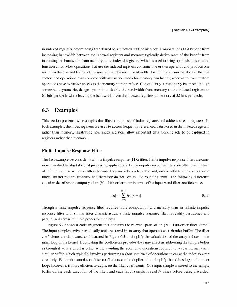
[ Section 6.3 – Examples ]
in indexed registers before being transferred to a function unit or memory. Computations that benefit fromincreasing bandwidth between the indexed registers and memory typically derive most of the benefit fromincreasing the bandwidth from memory to the indexed registers, which is used to bring operands closer to thefunction units. Most operations that use the indexed registers consume one or two operands and produce oneresult, so the operand bandwidth is greater than the result bandwidth. An additional consideration is that thevector load operations may compete with instruction loads for memory bandwidth, whereas the vector storeoperations have exclusive access to the memory store interface. Consequently, a reasonably balanced, thoughsomewhat asymmetric, design option is to double the bandwidth from memory to the indexed registers to64-bits per cycle while leaving the bandwidth from the indexed registers to memory at 32-bits per cycle.
6.3 Examples
This section presents two examples that illustrate the use of index registers and address-stream registers. Inboth examples, the index registers are used to access frequently referenced data stored in the indexed registersrather than memory, illustrating how index registers allow important data working sets to be captured inregisters rather than memory.
Finite Impulse Response Filter
The first example we consider is a finite impulse response (FIR) filter. Finite impulse response filters are com-mon in embedded digital signal processing applications. Finite impulse response filters are often used insteadof infinite impulse response filters because they are inherently stable and, unlike infinite impulse responsefilters, do not require feedback and therefore do not accumulate rounding error. The following differenceequation describes the output y of an (N−1)th order filter in terms of its input x and filter coefficients h.
y[n] =N−1
∑i=0
hix[n− i] (6.1)
Though a finite impulse response filter requires more computation and memory than an infinite impulseresponse filter with similar filter characteristics, a finite impulse response filter is readily partitioned andparallelized across multiple processor elements.
Figure 6.2 shows a code fragment that contains the relevant parts of an (N − 1)th-order filter kernel.The input samples arrive periodically and are stored in an array that operates as a circular buffer. The filtercoefficients are duplicated as illustrated in Figure 6.3 to simplify the calculation of the array indices in theinner loop of the kernel. Duplicating the coefficients provides the same effect as addressing the sample bufferas though it were a circular buffer while avoiding the additional operations required to access the array as acircular buffer, which typically involves performing a short sequence of operations to cause the index to wrapcircularly. Either the samples or filter coefficients can be duplicated to simplify the addressing in the innerloop; however it is more efficient to duplicate the filter coefficients. One input sample is stored to the samplebuffer during each execution of the filter, and each input sample is read N times before being discarded.
113
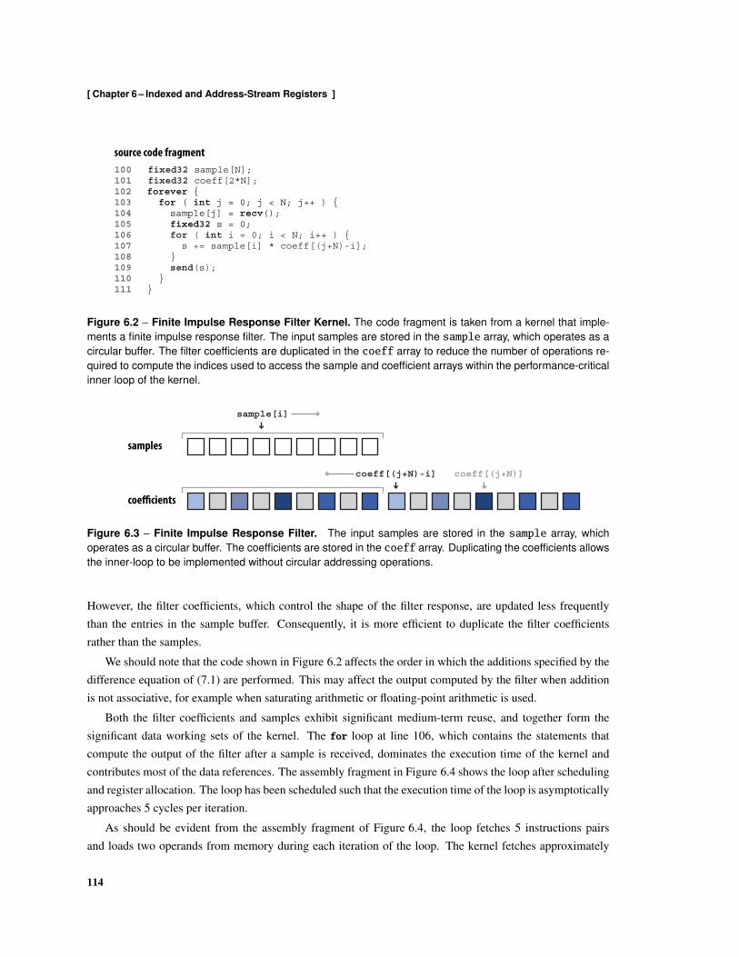
[ Chapter 6 – Indexed and Address-Stream Registers ]
source code fragment100101102103104105106107108109
forever { for ( int j = 0; j < N; j++ ) { sample[j] = recv(); fixed32 s = 0; for ( int i = 0; i < N; i++ ) { s += sample[i] * coeff[(j+N)-i]; } send(s); }}
fixed32 sample[N];
110111
fixed32 coeff[2*N];
Figure 6.2 – Finite Impulse Response Filter Kernel. The code fragment is taken from a kernel that imple-ments a finite impulse response filter. The input samples are stored in the sample array, which operates as acircular buffer. The filter coefficients are duplicated in the coeff array to reduce the number of operations re-quired to compute the indices used to access the sample and coefficient arrays within the performance-criticalinner loop of the kernel.
samples
coe!cients
coeff[(j+N)]
sample[i]
coeff[(j+N)-i]
Figure 6.3 – Finite Impulse Response Filter. The input samples are stored in the sample array, whichoperates as a circular buffer. The coefficients are stored in the coeff array. Duplicating the coefficients allowsthe inner-loop to be implemented without circular addressing operations.
However, the filter coefficients, which control the shape of the filter response, are updated less frequentlythan the entries in the sample buffer. Consequently, it is more efficient to duplicate the filter coefficientsrather than the samples.
We should note that the code shown in Figure 6.2 affects the order in which the additions specified by thedifference equation of (7.1) are performed. This may affect the output computed by the filter when additionis not associative, for example when saturating arithmetic or floating-point arithmetic is used.
Both the filter coefficients and samples exhibit significant medium-term reuse, and together form thesignificant data working sets of the kernel. The for loop at line 106, which contains the statements thatcompute the output of the filter after a sample is received, dominates the execution time of the kernel andcontributes most of the data references. The assembly fragment in Figure 6.4 shows the loop after schedulingand register allocation. The loop has been scheduled such that the execution time of the loop is asymptoticallyapproaches 5 cycles per iteration.
As should be evident from the assembly fragment of Figure 6.4, the loop fetches 5 instructions pairsand loads two operands from memory during each iteration of the loop. The kernel fetches approximately
114
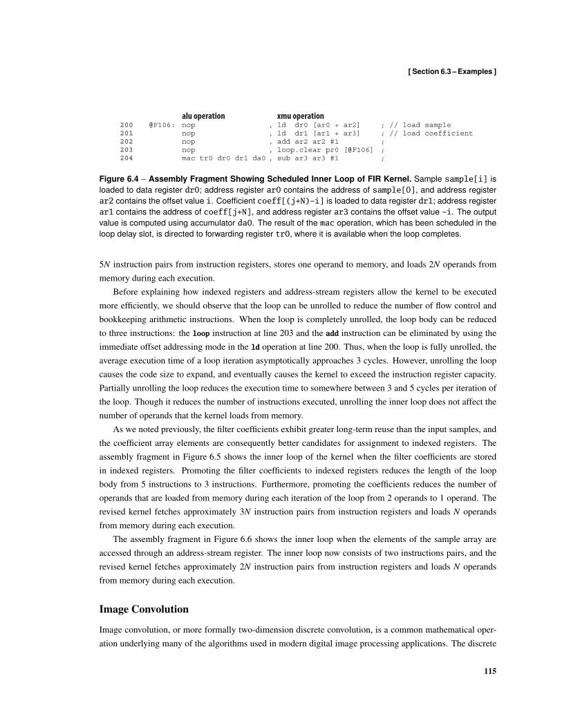
[ Section 6.3 – Examples ]
ld dr0 [ar0 + ar2]ld dr1 [ar1 + ar3]
mac tr0 dr0 dr1 da0
add ar2 ar2 #1
sub ar3 ar3 #1loop.clear pr0 [@F106]
,,,,,
; // load sample; // load coefficient;;;
200201202203204
@F106: nopnopnopnop
alu operation xmu operation
Figure 6.4 – Assembly Fragment Showing Scheduled Inner Loop of FIR Kernel. Sample sample[i] isloaded to data register dr0; address register ar0 contains the address of sample[0], and address registerar2 contains the offset value i. Coefficient coeff[(j+N)-i] is loaded to data register dr1; address registerar1 contains the address of coeff[j+N], and address register ar3 contains the offset value -i. The outputvalue is computed using accumulator da0. The result of the mac operation, which has been scheduled in theloop delay slot, is directed to forwarding register tr0, where it is available when the loop completes.
5N instruction pairs from instruction registers, stores one operand to memory, and loads 2N operands frommemory during each execution.
Before explaining how indexed registers and address-stream registers allow the kernel to be executedmore efficiently, we should observe that the loop can be unrolled to reduce the number of flow control andbookkeeping arithmetic instructions. When the loop is completely unrolled, the loop body can be reducedto three instructions: the loop instruction at line 203 and the add instruction can be eliminated by using theimmediate offset addressing mode in the ld operation at line 200. Thus, when the loop is fully unrolled, theaverage execution time of a loop iteration asymptotically approaches 3 cycles. However, unrolling the loopcauses the code size to expand, and eventually causes the kernel to exceed the instruction register capacity.Partially unrolling the loop reduces the execution time to somewhere between 3 and 5 cycles per iteration ofthe loop. Though it reduces the number of instructions executed, unrolling the inner loop does not affect thenumber of operands that the kernel loads from memory.
As we noted previously, the filter coefficients exhibit greater long-term reuse than the input samples, andthe coefficient array elements are consequently better candidates for assignment to indexed registers. Theassembly fragment in Figure 6.5 shows the inner loop of the kernel when the filter coefficients are storedin indexed registers. Promoting the filter coefficients to indexed registers reduces the length of the loopbody from 5 instructions to 3 instructions. Furthermore, promoting the coefficients reduces the number ofoperands that are loaded from memory during each iteration of the loop from 2 operands to 1 operand. Therevised kernel fetches approximately 3N instruction pairs from instruction registers and loads N operandsfrom memory during each execution.
The assembly fragment in Figure 6.6 shows the inner loop when the elements of the sample array areaccessed through an address-stream register. The inner loop now consists of two instructions pairs, and therevised kernel fetches approximately 2N instruction pairs from instruction registers and loads N operandsfrom memory during each execution.
Image Convolution
Image convolution, or more formally two-dimension discrete convolution, is a common mathematical oper-ation underlying many of the algorithms used in modern digital image processing applications. The discrete
115

[ Chapter 6 – Indexed and Address-Stream Registers ]
ld dr0 [ar0 + ar2]
mac tr0 dr0 xp0 da0 add ar2 ar2 #1loop.clear pr0 [@F106]
,,,
; // load sample;;
300301302
@F106: nopnop
alu operation xmu operation
Figure 6.5 – Assembly Fragment Showing use of Index Registers in Inner Loop of fir Kernel. Samplesample[i] is loaded to data register dr0; address register ar0 contains the address of sample[0], andaddress register ar2 contains the offset value i. The filter coefficients are stored in indexed registers, andcoefficient coeff[(j+N)-i] is accessed through index register xp0. The output value is computed usingaccumulator da0. The result of the mac operation, which has been scheduled in the loop delay slot, is directedto forwarding register tr0, where it is available when the loop completes.
ld dr0 [as0]mac tr0 dr0 xp0 da0 loop.clear pr0 [@F106], ;
400401 @F106:
alu operation xmu operation
nopld dr0 [as0]nop
402
,
,
; // load sample
mac tr0 dr0 xp0 da0 nop ;,; // load sample
403
Figure 6.6 – Assembly Fragment Showing use of Address-stream Registers in Inner Loop of fir Ker-nel. The scheduled loop body comprises the two instruction pairs at lines 401 and 402. The instruction pair atline 400 precedes the loop body and initiates the first loop iteration, and the instruction pair at line 403 followsthe loop body and completes the last loop iteration. Sample sample[i] is loaded to data register dr0 usingaddress-stream register as0 to generate the address sequence. The filter coefficients are stored in indexedregisters and accessed through index register xp0. The result of the mac operation, which has been scheduledin the loop delay slot, is directed to forwarding register tr0, where it is available when the loop completes.
convolution operation computes an image O from an image I and a function H according to the followingexpression.
O(y,x) = ∑u
∑v
I(y+ v,x+u) ·H(v,u) (6.2)
The values of H are often referred to as the filter weights or the convolution kernel. We shall use the termfilter to avoid confusion with the computation kernel that implements the convolution. The code fragmentshown in Figure 6.8 illustrates the application of a convolution kernel to an input image. The code computesoutput image o_img by convolving input image i_img with the M×M filter h. The code contains two loopnests: an outer loop nest with a domain that corresponds to elements of the output image, and an inner loopnest with a domain that corresponds to the elements of the filter h. The input image is padded with an N-element wide frame so that the output of the convolution is well-defined over the entire range of the outputimage. Figure 6.7 illustrates the padding, and highlights the working sets associated with the computation ofa single element in the output image.
To examine how address-stream registers and indexed registers allow image convolution to be performedmore efficiently, we shall examine the number of arithmetic operations and memory accesses required toperform image convolution. To make the example concrete, we will assume that the convolution applies a3×3 convolution kernel to a 256×256 image. This corresponds to setting N = 1, M = 3, and X = Y = 256in the source code of Figure 6.8.
The computation required by the convolution operations is dominated by multiplication and addition
116
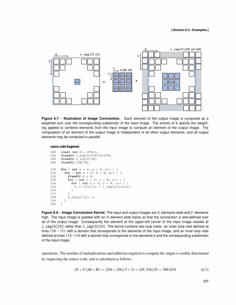
[ Section 6.3 – Examples ]
[x,y]
[0,0] [0,1] [0,2]
[1,0] [1,1] [1,2]
[2,0] [2,1] [2,2]
[x,y]
u
v
X
Y
= *
h[M][M]
o_img[Y][X]X
Y
i_img[Y+2N][X+2N]
Figure 6.7 – Illustration of Image Convolution. Each element of the output image is computed as aweighted sum over the corresponding subdomain of the input image. The entries of h specify the weight-ing applied to combine elements from the input image to compute an element of the output image. Thecomputation of an element of the output image is independent of all other output elements, and all outputelements may be computed in parallel.
source code fragment
101
103
110111112113114115116
for ( int y = 0; y < Y; y++ ) { for ( int x = 0; x < X; x++ ) {
fixed32 s = 0;
for ( int u = 0; u < M; u++ ) {s += h[v][u] * i_img[y+v][x+u];
}}
}
fixed32 i_img[Y+2*N][X+2*N];
117118
fixed32 h[M][M];
for ( int v = 0; v < M; v++ ) {
100 const int M = 2*N+1;
120}119o_img[y][x]= s;
102 fixed32 o_img[Y][X];
Figure 6.8 – Image Convolution Kernel. The input and output images are X elements wide and Y elementshigh. The input image is padded with an N-element wide frame so that the convolution is well-defined overall of the output image. Consequently the element at the upper-left corner of the input image resides ati_img[N][N] rather than i_img[0][0]. The kernel contains two loop nests: an outer loop nest defined atlines 110 – 111 with a domain that corresponds to the elements of the input image, and an inner loop nestdefined at lines 113 –114 with a domain that corresponds to the elements h and the corresponding subdomainof the input image.
operations. The number of multiplications and additions required to compute the output is readily determinedby inspecting the source code, and is calculated as follows.
(X×Y )(M×M) = (256×256)(3×3) = (65,536)(9) = 589,824 (6.3)
117
[ Chapter 6 – Indexed and Address-Stream Registers ]
Each multiplication accesses one element of the input image and one coefficient of filter h. Consequently,the aggregate number of accesses to elements of the input image and the aggregate number of accesses toelements of h are also computed by equation (6.3). Though the aggregate number of accesses are equal, thereare more accesses to an individual element of h than an element of the input image, and the working setscorresponding to the element of h and the input image differ in significance. Each element of h contributesto the computation of the 65,536 elements of the output image, whereas an element of the input image onlycontributes the computation of 9 elements of the output image. Consequently, the working set comprising theelements of h exhibits significantly more reuse than the working sets comprising neighboring elements of theinput image.
An initial implementation of the image convolution kernel is shown in Figure 6.9. As should be apparentfrom the assembly fragment, the implementation shown in Figure 6.9 does not use the indexed registers andaddress-stream registers. The inner loop is completely unrolled, and comprises lines 203 – 209. The numberof instructions fetched when the code shown in Figure 6.9 executes is computed as follows.
256× (256× ((3×8)+4)+2) = 1,835,520 (6.4)
Similarly, the number of memory accesses required to fetch operands from memory and store results tomemory is computed as follows.
256× (256× ((3×6)+1)+0) = 1,245,184 (6.5)
Let us first consider using address-stream registers to eliminate some of the explicit address computations.Figure 6.10 shows an implementation of the image convolution kernel that uses the address-stream registers.The use of the address-stream registers eliminates one instruction from the for loop at line 111, whichadvances the output position across a row of the input image. The number of instructions fetched when thecode shown in Figure 6.10 executes is computed as follows.
256× (256× ((3×8)+3)+2) = 1,769,984 (6.6)
This corresponds to a modest 3.6% reduction in the number of instructions that are fetched. The number ofoperands fetched from memory remains unchanged.
Let us next consider using indexed registers to exploit reuse within the various data working sets ex-hibited by the image convolution kernel. Promoting the elements of the function h to indexed registers isrelatively straightforward because the access pattern is affine. Figure 6.11 shows an implementation of theimage convolution kernel that assigns the elements of the function h to indexed registers and uses address-stream registers to load elements of the input image and store elements of the output image. The number ofinstructions fetched when the code shown in Figure 6.11 executes is calculated as follows.
256× (256× (3×5+3)+2) = 1,180,160 (6.7)
118

[ Section 6.3 – Examples ]
ld dr0 [ar0 + 0]ld dr1 [ar1 + 0]
,,
,
200201202203204
@F113: nopnop
alu operation xmu operation
ld dr0 [ar0 + 1]ld dr1 [ar1 + 1]
,,
mac tr0 dr0 dr1 da0nopmac tr0 dr0 dr1 da0 ld dr0 [ar0 + 2]
ld dr1 [ar1 + 2],
add dr2 dr2 #3
mac tr0 dr0 dr1 da0
,loop.clear pr0 [@F113]add ar1 ar1 #258,
; // dr0 = h[v][0]; // dr1 = i_img[y+v][x+0]; // dr0 = h[u][1]; // dr1 = i_img[y+v][x+1]
mov ar0 tr2; // ar1 = &i_img[y+v][x]
; // dr2 = &h[v+1][0]; // v++
205206207208
mov ar1 tr0,
loop.clear pr1 [@F110] ; // x++
loop.clear pr2 [@F110] ; // y++
mov gr1 @i_img@F110:
mov dr2 @hmov ar0 dr2
,
mov dr2 @hst tr0 [ar3]
add ar3 ar3 #1
; // out[y][x] = s;mov da0 #0
add gr1 gr1 #1
add gr1 gr1 #2
,
,,
,, nop
nop
209210211212213214 ; // gr1 = &i_img[y][x]
; // ar3 = &o_img[y][x]
; // dr0 = h[u][2]
Figure 6.9 – Assembly Fragment for Convolution Kernel. The inner-most loop is completely unrolled.The instruction pairs at lines 202 – 208 comprise the body of the unrolled loop; operand registers dr0 anddr0 stage the image elements and filter coefficients as they are loaded from memory; address register ar0supplies addresses for loading image elements, and address register ar1 supplies addresses for loading filtercoefficients. Predicate register pr0 stores the loop with induction variable v and controls the execution of theloop at line 113 in the source code; predicate register pr1 stores the loop induction variable x and controls theexecution of the loop at line 111 predicate register pr2 stores the loop induction variable y and controls theexecution of the loop defined at line 110. The add operation at line 209 advances the pointer stored in ar1 tothe next row of the input image; the offset of 258 combines the image width (X=256) and the frame (2N=2).The st instruction at line 210 stores the value computed for the output image element; address register ar3provides the address of the next element in the output image. The add operation at line 214 advances thepointer stored in gr1 to the next row of the input image, correcting for the padding columns introduced alongthe left and right edges of the input image.
ld dr0 [as0]ld dr1 [ar0 + 0]
,,
,
300301302303304
@F113: nopnop
alu operation xmu operation
ld dr0 [as0]ld dr1 [ar0 + 1]
,,
mac tr0 dr0 dr1 da0nopmac tr0 dr0 dr1 da0 ld dr0 [as0]
ld dr1 [ar0 + 2],
mac ar3 dr0 dr1 da0,loop.clear pr0 [@F113]add ar0 ar1 as1,
; // dr0 = h[v][0]; // dr1 = i_img[y+v][x+0]; // dr0 = h[u][1]; // dr1 = i_img[y+v][x+1]
; // ar1 = &i_img[y+v][x]
; // dr1 = i_img[y+v][x+2]; // v++
305306307308
loop.clear pr1 [@F111] ; // x++
loop.clear pr2 [@F111] ; // y++; // out[y][x] = s;
,
,,
,
309310311312313
; // ar1 = &i_img[y][x]
; // ar0 = &i_img[y][x]
st ar3 [as3]mov da0 #0
nop
nop add ar0 ar1 as1@F110:
nop
, mov ar2 @i_img
,
nop
nopnopnop
, add ar1 ar2 as2nop@F111:
add ar1 ar2 as2
; // ar1 = &i_img[y][x]
314
; // dr0 = h[u][2]
Figure 6.10 – Assembly Fragment for Convolution Kernel using Address-Stream Registers. The assem-bly listing shows the code after loop unrolling.
This corresponds to a 33% reduction in the number of instructions fetched. The number of memory accessesperformed when the code executes is calculated as follows.
256× (256× (3×3+1)+0)+9 = 655,369 (6.8)
119

[ Chapter 6 – Indexed and Address-Stream Registers ]
ld dr1 [ar0 + 0],,
,
400401402403404
@F113: nop
alu operation xmu operation
ld dr1 [ar0 + 1],,
mac tr0 xr0 dr1 da0mac tr0 xr0 dr1 da0
,mac ar3 xr0 dr1 da0
,
loop.clear pr0 [@F113]add ar0 ar1 as1
,
; // dr1 = i_img[y+v][x+0]; // dr1 = i_img[y+v][x+1]
; // ar1 = &i_img[y+v][x]; // v++
405406407408 loop.clear pr1 [@F111] ; // x++
loop.clear pr2 [@F111] ; // y++; // out[y][x] = s;
,
409410411 ; // ar1 = &i_img[y][x]
; // ar0 = &i_img[y][x]
st ar3 [as3]mov da0 #0
nop add ar0 ar1 as1@F110:
nop
, mov ar2 @i_img
,
nop
nopnopnop
, add ar1 ar2 as2nop@F111:
add ar1 ar2 as2
; // ar1 = &i_img[y][x]
ld dr1 [ar0 + 2] ; // dr1 = i_img[y+v][x+1]
Figure 6.11 – Convolution Kernel using Indexed Registers. The assembly fragment shows the kernel afterloop unrolling.
Promoting the elements of h to indexed registers reduces the number of memory accesses performed to loadoperands and store data by 47%.
To capture reuse of the image samples, we interchange the loops in the inner loop nest so that M sam-ples from a single column are transferred to the indexed registers in each iteration of the outer loop nest.Figure 6.13 illustrates the pattern of reuse in the indexed registers. Interchanging the order of the inner loopnest complicates the computation of addresses, though the address-stream registers absorb most of the com-plexity. We could instead interchange the order of the loops in the outer loop nest, though doing so wouldaffect the order in which elements of the input image would need to be streamed to the convolution kernel toavoid buffering most of the image before initiating the kernel. For example, an implementation of the imageconvolution kernel that proceeds down a column before advancing to the next row would need to buffer mostof the input image when the input image is transferred by streaming elements along rows corresponding tohorizontal scan lines.
Figure 6.12 shows the resulting assembly code fragment. The number of instructions fetched when thecode executes is calculated as follows.
256× (256× (3×3+3)+4) = 787,456 (6.9)
This corresponds to a further 33% reduction in the number of instructions fetched, and a cumulative reductionof 57% from the initial implementation. The number of memory accesses performed is calculated as follows.
256× (256× (3×0+5)+0)+15 = 327,695 (6.10)
Using the indexed registers to capture reuse within the elements of the input image further reduces the numberof memory accesses by 50%, and achieves a cumulative reduction of 74%.
120
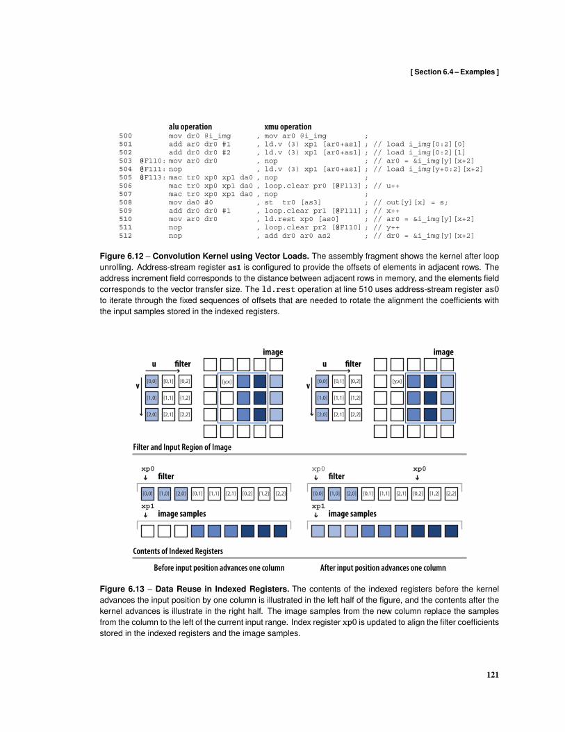
[ Section 6.4 – Examples ]
ld.v (3) xp1 [ar0+as1],,
,
500501502503504
@F113:nop
alu operation xmu operation
,,
mac tr0 xp0 xp1 da0mac tr0 xp0 xp1 da0
,mac tr0 xp0 xp1 da0
,
loop.clear pr0 [@F113]
ld.rest xp0 [as0],
;
505506507508
loop.clear pr1 [@F111] ; // x++
loop.clear pr2 [@F110] ; // y++
; // out[y][x] = s;
,
509510
st tr0 [as3]mov da0 #0
,mov dr0 @i_img
mov ar0 dr0nopnop
,
@F111:
; // u++ nop
nop
add dr0 dr0 #1
; // load i_img[y+0:2][x+2]
add dr0 ar0 as2
; // ar0 = &i_img[y][x+2]
mov ar0 @i_imgld.v (3) xp1 [ar0+as1]
, ld.v (3) xp1 [ar0+as1]add ar0 dr0 #1add dr0 dr0 #2
,mov ar0 dr0 nop@F110:
511512
;
;
; // load i_img[0:2][0]; // load i_img[0:2][1]; // ar0 = &i_img[y][x+2]
; // dr0 = &i_img[y][x+2]
Figure 6.12 – Convolution Kernel using Vector Loads. The assembly fragment shows the kernel after loopunrolling. Address-stream register as1 is configured to provide the offsets of elements in adjacent rows. Theaddress increment field corresponds to the distance between adjacent rows in memory, and the elements fieldcorresponds to the vector transfer size. The ld.rest operation at line 510 uses address-stream register as0to iterate through the fixed sequences of offsets that are needed to rotate the alignment the coefficients withthe input samples stored in the indexed registers.
[0,0] [0,1] [0,2]
[1,0] [1,1] [1,2]
[2,0] [2,1] [2,2]
u
v
!lter image
[0,0] [1,0] [2,0] [0,1] [1,1] [2,1] [0,2] [1,2] [2,2]
xp0
xp1
[0,0] [0,1] [0,2]
[1,0] [1,1] [1,2]
[2,0] [2,1] [2,2]
u
v
!lter image
[0,0] [1,0] [2,0] [0,1] [1,1] [2,1] [0,2] [1,2] [2,2]
xp0
xp1
xp0
[y,x] [y,x]
!lter
image samples
!lter
image samples
Before input position advances one column After input position advances one column
Contents of Indexed Registers
Filter and Input Region of Image
Figure 6.13 – Data Reuse in Indexed Registers. The contents of the indexed registers before the kerneladvances the input position by one column is illustrated in the left half of the figure, and the contents after thekernel advances is illustrate in the right half. The image samples from the new column replace the samplesfrom the column to the left of the current input range. Index register xp0 is updated to align the filter coefficientsstored in the indexed registers and the image samples.
121

[ Chapter 6 – Indexed and Address-Stream Registers ]
aes conv2d crc crosscor dct !r hu"man jpeg rgb2yuv viterbi0
64
128
256
32
default using address-stream registers using indexed and address-stream registers
Figure 6.14 – Static Kernel Code Size. The static kernel code size includes load instructions that are requiredto initialize the index and address-stream registers when a kernel begins executing.
6.4 Evaluation and Analysis
This section provides an evaluation and analysis of the Elm indexed registers and address-stream registers.The kernels used in the evaluation were compiled using elmcc. We present various performance and ef-ficiency results for three processor configurations. The default configuration uses neither address-streamregisters nor index registers, and provides a reference for comparison. The configuration labeled as usingaddress-stream registers has 4 address-stream registers in addition to the general-purpose and operand reg-isters, but does not use the index registers. The configuration labeled as using indexed and address-streamregisters has 4 index registers in addition to the 4 address-stream registers of the previous configuration.
Static Code Size
Address-stream registers and indexed registers allow software to eliminate bookkeeping and memory oper-ations. Figure 6.14 shows the static instruction counts for each of the kernels, and illustrates the impact ofcompiling the kernels to use address-stream registers and indexed registers on static code. The size reportedfor each kernel corresponds to the number of instruction pairs in the assembly code produced by the com-piler, and includes instruction pairs that are inserted into the prologue and epilogue to configure any of theaddress-stream and index registers used by the kernel.
Using address-stream registers consistently reduces the static kernel code size, though the significanceof the reduction depends on how many bookkeeping instructions are eliminated. All of the kernels listedare able to use address-stream registers to eliminate some explicit bookkeeping instructions. For kernels inwhich the use of address-stream registers is limited to iterating sequentially through the input and outputdata buffers, such as huffman and jpeg, the elimination of a modest number of bookkeeping instructions isoffset by the introduction of instructions to initialize the address-stream registers; consequently, compiling
122

[ Section 6.4 – Evaluation and Analysis ]
default using address-stream registers using indexed and address-stream registers
aes conv2d crc crosscor dct !r hu"man jpeg rgb2yuv viterbi0.0
0.2
0.4
0.6
0.8
1.0
Figure 6.15 – Dynamic Kernel Instruction Count. The dynamic kernel instruction includes instructions thatare executed to initialize the index and address-stream registers.
the kernels to use address-stream registers provides a modest reduction in the static code size. For kernels inwhich address-stream registers are used to eliminate bookkeeping instructions throughout the kernel, such ascrosscor and rgb2yuv, eliminating bookkeeping instructions reduces the static kernel code size by 33% to40%.
Using index and indexed registers consistently eliminates load and store instructions in those kernels withworking sets that can be captured in the indexed registers; however, the additional instructions required toinitialize and manage the index registers partially offsets the reduction in the code size. The increase in thestatic code size of the conv2d and crosscor kernels results from restructuring the kernels to enhance the useof the indexed registers. To allow samples from the input image to be stored in indexed registers, the orderof the loops that implement the filter computation in the conv2d kernel is interchanged so that samples in acolumn are loaded to adjacent indexed registers. This reduces the number of times each sample is loaded,but requires additional address-stream registers, which must be initialized when in the kernel prologue. Theincrease in the static code size of the crosscor kernel results from restructuring the computation to computemultiple cross-correlation coefficients in parallel. The initial version computes a single cross-correlationcoefficient, storing the coefficient being calculated in a dedicated accumulator and using multiply-accumulateoperations to update the coefficient. Using the indexed registers to compute multiple coefficients in parallelallows an input sample to be incorporated into multiple coefficients after being loaded, reducing the numberof times each input sample is loaded. For both kernels, restructuring the computation introduces additionalinstructions outside the important loops, which accounts for the increase in the static code size.
123
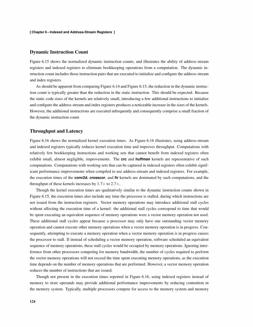
[ Chapter 6 – Indexed and Address-Stream Registers ]
Dynamic Instruction Count
Figure 6.15 shows the normalized dynamic instruction counts, and illustrates the ability of address-streamregisters and indexed registers to eliminate bookkeeping operations from a computation. The dynamic in-struction count includes those instruction pairs that are executed to initialize and configure the address-streamand index registers.
As should be apparent from comparing Figure 6.14 and Figure 6.15, the reduction in the dynamic instruc-tion count is typically greater than the reduction in the static instruction. This should be expected. Becausethe static code sizes of the kernels are relatively small, introducing a few additional instructions to initializeand configure the address-stream and index registers produces a noticeable increase in the sizes of the kernels.However, the additional instructions are executed infrequently and consequently comprise a small fraction ofthe dynamic instruction count.
Throughput and Latency
Figure 6.16 shows the normalized kernel execution times. As Figure 6.16 illustrates, using address-streamand indexed registers typically reduces kernel execution time and improves throughput. Computations withrelatively few bookkeeping instructions and working sets that cannot benefit from indexed registers oftenexhibit small, almost negligible, improvements. The crc and huffman kernels are representative of suchcomputations. Computations with working sets that can be captured in indexed registers often exhibit signif-icant performance improvements when compiled to use address-stream and indexed registers. For example,the execution times of the conv2d, crosscor, and fir kernels are dominated by such computations, and thethroughput of these kernels increases by 1.7× to 2.7×.
Though the kernel execution times are qualitatively similar to the dynamic instruction counts shown inFigure 6.15, the execution times also include any time the processor is stalled, during which instructions arenot issued from the instruction registers. Vector memory operations may introduce additional stall cycleswithout affecting the execution time of a kernel: the additional stall cycles correspond to time that wouldbe spent executing an equivalent sequence of memory operations were a vector memory operation not used.These additional stall cycles appear because a processor may only have one outstanding vector memoryoperation and cannot execute other memory operations when a vector memory operation is in progress. Con-sequently, attempting to execute a memory operation when a vector memory operation is in progress causesthe processor to stall. If instead of scheduling a vector memory operation, software scheduled an equivalentsequence of memory operations, these stall cycles would be occupied by memory operations. Ignoring inter-ference from other processors competing for memory bandwidth, the number of cycles required to performthe vector memory operations will not exceed the time spent executing memory operations, as the executiontime depends on the number of memory operations that are performed. However, a vector memory operationreduces the number of instructions that are issued.
Though not present in the execution times reported in Figure 6.16, using indexed registers instead ofmemory to store operands may provide additional performance improvements by reducing contention inthe memory system. Typically, multiple processors compete for access to the memory system and memory
124
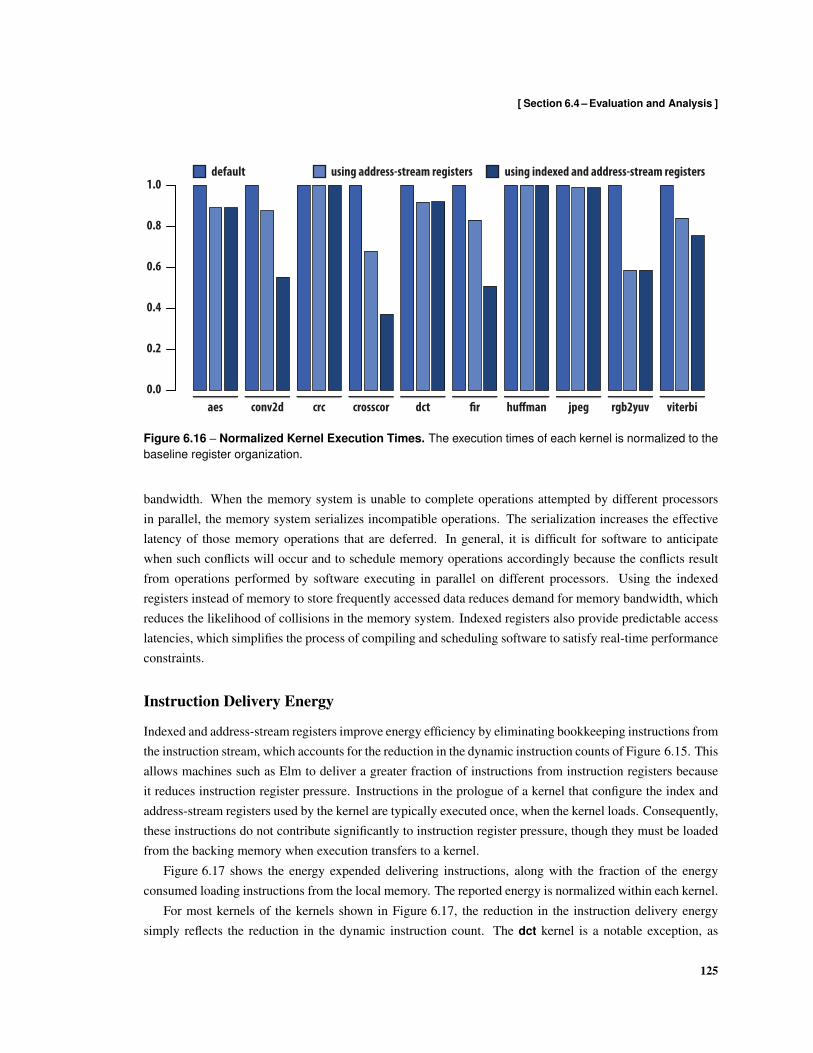
[ Section 6.4 – Evaluation and Analysis ]
aes conv2d crc crosscor dct !r hu"man jpeg rgb2yuv viterbi0.0
0.2
0.4
0.6
0.8
1.0default using address-stream registers using indexed and address-stream registers
Figure 6.16 – Normalized Kernel Execution Times. The execution times of each kernel is normalized to thebaseline register organization.
bandwidth. When the memory system is unable to complete operations attempted by different processorsin parallel, the memory system serializes incompatible operations. The serialization increases the effectivelatency of those memory operations that are deferred. In general, it is difficult for software to anticipatewhen such conflicts will occur and to schedule memory operations accordingly because the conflicts resultfrom operations performed by software executing in parallel on different processors. Using the indexedregisters instead of memory to store frequently accessed data reduces demand for memory bandwidth, whichreduces the likelihood of collisions in the memory system. Indexed registers also provide predictable accesslatencies, which simplifies the process of compiling and scheduling software to satisfy real-time performanceconstraints.
Instruction Delivery Energy
Indexed and address-stream registers improve energy efficiency by eliminating bookkeeping instructions fromthe instruction stream, which accounts for the reduction in the dynamic instruction counts of Figure 6.15. Thisallows machines such as Elm to deliver a greater fraction of instructions from instruction registers becauseit reduces instruction register pressure. Instructions in the prologue of a kernel that configure the index andaddress-stream registers used by the kernel are typically executed once, when the kernel loads. Consequently,these instructions do not contribute significantly to instruction register pressure, though they must be loadedfrom the backing memory when execution transfers to a kernel.
Figure 6.17 shows the energy expended delivering instructions, along with the fraction of the energyconsumed loading instructions from the local memory. The reported energy is normalized within each kernel.
For most kernels of the kernels shown in Figure 6.17, the reduction in the instruction delivery energysimply reflects the reduction in the dynamic instruction count. The dct kernel is a notable exception, as
125
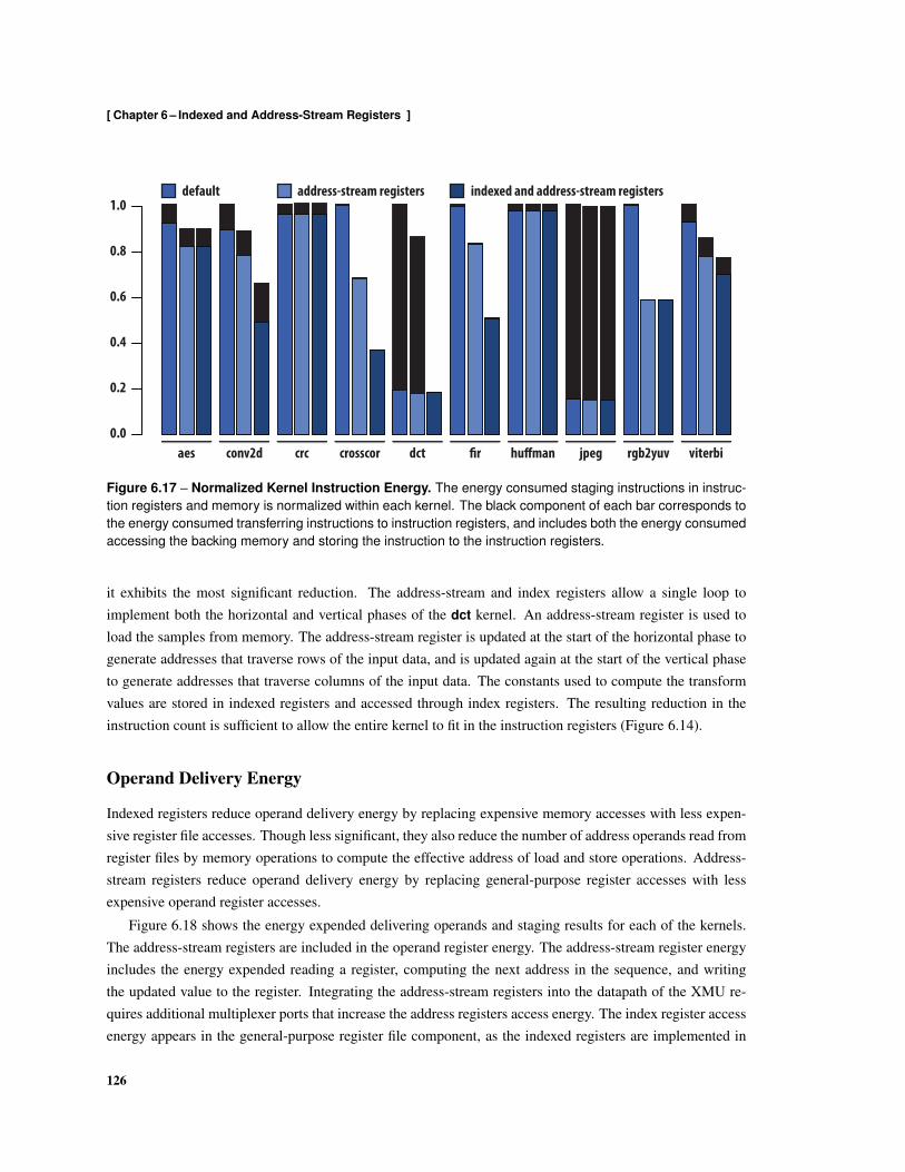
[ Chapter 6 – Indexed and Address-Stream Registers ]
default address-stream registers indexed and address-stream registers
aes conv2d crc crosscor dct !r hu"man jpeg rgb2yuv viterbi0.0
0.2
0.4
0.6
0.8
1.0
Figure 6.17 – Normalized Kernel Instruction Energy. The energy consumed staging instructions in instruc-tion registers and memory is normalized within each kernel. The black component of each bar corresponds tothe energy consumed transferring instructions to instruction registers, and includes both the energy consumedaccessing the backing memory and storing the instruction to the instruction registers.
it exhibits the most significant reduction. The address-stream and index registers allow a single loop toimplement both the horizontal and vertical phases of the dct kernel. An address-stream register is used toload the samples from memory. The address-stream register is updated at the start of the horizontal phase togenerate addresses that traverse rows of the input data, and is updated again at the start of the vertical phaseto generate addresses that traverse columns of the input data. The constants used to compute the transformvalues are stored in indexed registers and accessed through index registers. The resulting reduction in theinstruction count is sufficient to allow the entire kernel to fit in the instruction registers (Figure 6.14).
Operand Delivery Energy
Indexed registers reduce operand delivery energy by replacing expensive memory accesses with less expen-sive register file accesses. Though less significant, they also reduce the number of address operands read fromregister files by memory operations to compute the effective address of load and store operations. Address-stream registers reduce operand delivery energy by replacing general-purpose register accesses with lessexpensive operand register accesses.
Figure 6.18 shows the energy expended delivering operands and staging results for each of the kernels.The address-stream registers are included in the operand register energy. The address-stream register energyincludes the energy expended reading a register, computing the next address in the sequence, and writingthe updated value to the register. Integrating the address-stream registers into the datapath of the XMU re-quires additional multiplexer ports that increase the address registers access energy. The index register accessenergy appears in the general-purpose register file component, as the indexed registers are implemented in
126

[ Section 6.5 – Evaluation and Analysis ]
0.0
0.2
0.4
0.6
0.8
1.0
aes conv2d crc crosscor dct !r hu"man jpeg rgb2yuv viterbi
hardware forward operand register general-purpose register memoryexplicit forward
D XA D XA D XA D XA D XA D XA D XA D XA D XA D XA
Figure 6.18 – Normalized Kernel Data Energy. The energy consumed staging data in registers and memoryis normalized within each kernel. The three bars within each kernel, from left to right, correspond to thebaseline register organization; the baseline organization extended with address-stream registers; and thebaseline organization extended with both address-stream registers and index registers.
the general-purpose register file. The index register access energy includes the energy expended reading theindex registers, updating the index, and writing the updated index back to the index register. Integrating theindex registers and the general-purpose register file requires additional multiplexers and logic to control theselection of the addresses sent to the general-purpose register file. The additional logic increases the cost ofaccessing operands stored in general-purpose registers.
The most significant reductions in operand energy arise when operands are assigned to indexed registersinstead of memory. For example, the index registers provide a 91% reduction in operand energy for thecrosscor kernel beyond the 12% reduction provided by the address-stream registers. Similarly, the indexedregisters provide a 92% reduction for the fir kernel beyond the 7% reduction provided by the address-streamregisters. As the operand energy is dominated by memory accesses without the indexed registers, indexedregisters would provide greater reductions were a more expensive memory used as the local memory. Forexample, the reduction would be greater were a cache memory or a software-managed memory of greatercapacity used as a local memory.
The address-stream registers reduce the energy expended delivering operands for the aes and jpeg kernelsby allowing additional operands to be stored in operand registers rather than more expensive general-purposeregisters. The increase in the operand energy incurred in the indexed register configuration results from theincreased cost of accessing the general-purpose registers.
127

[ Chapter 6 – Indexed and Address-Stream Registers ]
6.5 Related Work
Vector processors [123] provide large collections of physical registers that are accessed indirectly as elementsof vector registers [10, 59]. Because many important kernels in embedded and multimedia applications arevectorizable, the register organizations used in vector processors are able to capture a significant fraction ofintra-kernel reuse and locality in embedded applications [84]. Contemporary vector-processor architecturessupport both vector and multithreaded execution models [88, 120]. For example, the Scale Vector-Threadarchitecture [88] supports both vector and multithread compute models using a collection of processors toimplement a vector of virtual processors when operating as a vector processor. Like Elm, the Scale Vector-Thread architecture provides both registers that are accessed directly (shared registers) and registers that areaccessed indirectly (private registers) using virtual register specifiers, and allows software to configure theallocation of physical registers between the sets of directly and indirectly accessed registers. Contemporarygraphics processing unit architectures also allow physical registers to be dynamically partitioned amongthread contexts, though typically this is managed by dedicated hardware or device-level software [41].
Stream processors such as Imagine [121] provide a large software-managed stream register file that isaccessed indirectly through stream buffers. The stream register file is partitioned among multiple activestreams, and software controls the allocation of entries in the stream register file to streams. The streamregister file is used to stage bulk data transfers between memory and local registers distributed among thefunction units. It is also used to temporarily store elements of streams transferred between computationkernels to avoid transferring intermediate data to memory. This allows a stream register file to be used tocapture inter-kernel producer-consumer locality, and reduces off-chip memory bandwidth. Because a streamregister file must be large enough to stage data between memory and the stream processor, stream registerfiles are much larger than the indexed register files used in Elm.
The early reduced instruction set computer (RISC) architectures [114] used register windows to providesoftware access to more physical registers than could be encoded directly in an instruction. Register win-dow organizations typically partition the physical registers into a set of global registers and multiple sets ofoverlapping windows. Register windows provide software with the abstraction of an unbounded stack ofwindows, though only a subset near the top of the stack are maintained in physical registers; the remainingwindows must be stored in memory. A distinguished control register determines which of the physical reg-ister window is active. Procedure call and return instructions implicitly update the active window, with callinstructions allocating a new set of registers for use by the called procedure. Should the physical registersassigned to the new window be in use when a call instruction executes, the contents of the registers are trans-ferred to memory and must later be restored. Privileged software may explicitly modify the active registerwindow, typically to end a spill or fill trap handler. Register windows continue to be used in contemporaryUltraSPARC architectures [104].
Itanium implements hardware-managed register stacks [28]. The register stack mechanism is similar tothe register window scheme described previously. The architecture partitions the general register file into astatic and stacked subset. The static subset is visible to all procedures; the stacked subset is local to eachprocedure and may vary in size from 0 to 96 registers. The register stack mechanism is implemented by
128
[ Section 6.5 – Related Work ]
renaming register addresses during procedure call and return operations. Registers in the register stack areautomatically saved and restored by a hardware register stack engine.
In addition to register stacks, Itanium implements a rotating register file mechanism for use in software-pipelined loops [118, 119]. A single architectural register in the rotating portion of the register file may beused in place of multiple architectural registers to specify instances of a variable defined by different iterationsof a loop. Equivalent software techniques such as modulo variable expansion [93] introduce a unique namefor each simultaneously live instance of a variable so that values defined in different iterations of a loop canbe distinguished. This increases architectural register requirements and expands code size, as a sufficientnumber of interleaved iterations of the loop body must be introduced to accommodate the naming constraintsof the software-pipelined loop.
Itanium allows a fixed-sized region of the floating-point register files and a programmable-sized regionof the general register file to rotate when a software-pipelined loop type branch executes. The rotation isimplemented by renaming register addresses based on the value of rotating register base field contained in acontrol register. Each rotation decrements the contents of the affected rotating register base values modulothe size of their respective software-defined rotating regions. Aside from the change of the rotating registerbase values, the rotating register mechanism is not visible to software.
Along with other features that distinguish explicitly parallel instruction computing (EPIC) architecturessuch as Itanium from their VLIW ancestors, rotating registers were introduced to improve the performanceof processors in which the compiler explicitly exploits instruction-level parallelism. Rotating registers wereoriginally used in the Hewlett-Packard Laboratories PlayDoh architecture to improve the code density ofsoftware-pipelined loops [76]. These early EPIC style architectures originated as parametric processor ar-chitectures, developed to enable an embedded system design paradigm in which a compiler generates anapplication-specific processor for an embedded application [126]. This allows a system designer to describean embedded system in a high-level programming language. Essentially, in addition to compiling an appli-cation, the compiler generates a set of specific bindings for processor parameters. Similar strategies havebeen adapted for designing customized chip-multiprocessors [136] and digital signal processors for embed-ded systems from descriptions of applications provided in high-level programming languages; for example,the AnySP signal processor relies on a similar strategy of customizing hardware for a specific application toimprove efficiency [150].
Register queues provide an alternative mechanism to rotating registers for decoupling physical registersfrom architectural register names so that more physical registers can be provisioned, improving the applicabil-ity of software-pipelining [132]. Register queue architectures let software construct queues in the register fileto buffer multiple live instances of a variable introduced during modulo variable expansion. Register queuearchitectures require hardware tables for recording the mapping of architectural register names to physicalregisters and register queues, and for mapping each appearance of an architectural register that has beenmapped to a register queue to an appropriate offset within its associated queue. Index and indexed registerscan be used to achieve a similar decoupling of physical registers and architectural register names, to parti-tion physical registers among architectural register names, and to implement queues for decoupling memoryoperations.
129
[ Chapter 6 – Indexed and Address-Stream Registers ]
In contemporary computer systems, software pipelining delivers greater performance improvements whenused to tolerate memory access latencies rather than arithmetic unit latencies, which are short compared totypical memory access times. The number of physical registers required for a compiler to software pipeline aloop effectively increases as the product of the number of variables in the loop and the number of interleavedloop iterations. The additional physical registers provided by a rotating register file allow software to schedulemore interleaved loop iterations. As the number of interleaved iterations required to tolerate the latencyof operations in a loop increases with the operation latencies, additional physical registers allow softwarepipelining to tolerate longer function unit latencies. In addition to tolerating memory access latency, indexedregisters let software effectively capture medium-term reuse and locality in local register files rather thanmemory, which is considerably more difficult to achieve using rotating register files and register queues.
The VICTORIA [37] architecture defines a set of extensions to VMX, the SIMD extensions to the Pow-erPC architecture [27], that uses indirection to increase the number of VMX registers that are available tosoftware. The indirect-VMX (iVMX) extensions allow a processor to implement as many as 4,096 VMXregisters. The extensions define several sets of map registers that store offsets into the VMX register file.The map registers are organized as tables that are indexed using the VMX register specifier encoded in aninstruction. An independent map table is maintained for each of the 4 register specifier fields defined by theVMX extensions. The effective address of a VMX register is computed by adding the offset stored in theassociated map register and the address encoded in the register specifier field of an instruction. Softwareis responsible for managing the map registers, and must explicitly modify map registers to access a differ-ent subset of the extended VMX registers, which limits the number of VMX registers that can be accessedwithout executing bookkeeping instructions that modify the map registers. However, the extensions preservebackwards compatibility with the original VMX extensions.
The eLite digital signal processor [106] provides a collection of vector pointer registers that are used toindex a set of vector element registers. Like the index registers described in this chapter, the vector pointerregisters are automatically updated when used to access the vector element registers. However, the eLitearchitecture supports a single-instruction multiple-data SIMD execution model in which instructions operateon disjoint data that are packed into short fixed-width vectors. The architecture uses a distinguished set ofvector accumulator registers to receive the results of most vector operations, with the perhaps obvious ex-ception of operations that transfer vector accumulator registers to vector element registers and to memory.The vector element registers are organized to allow data in vector element registers to be arbitrarily packedinto operand vectors as they are read from the vector element register file. Every access to the vector ele-ment registers is performed indirectly through the vector pointer registers, and each of the 4 elements in apacked operand may use a different pointer value to access the vector element register file. This supports avector programming model in which data in memory and in the vector accumulator registers are accessedas packed vector elements, while data stored in the vector element registers are accessed as scalar elementsthat are packed into vector operands on access. The creators of the eLite architecture refer to this as a regis-ter organization that supports single-instruction multiple disjoint data SIMdD operations, as opposed to theconventional single-instruction multiple packed data SIMpD multimedia instruction sets found in commodityprocessors. The eLite register organization allows data reuse that crosses vector lanes to be captured in the
130

[ Section 6.6 – Chapter Summary ]
vector element register file without performing explicit permutation operations or memory operations to alignvector elements. However, it does so by introducing additional register file ports. Each vector lane has its owndedicated read and write ports to the vector element register file. Though the impact of the additional ports onthe area and access energy of the vector register file organization is not quantified, the additional ports renderthe vector element registers less area-efficient and less energy-efficient than a conventional SIMD registerorganization[122]. The register organization also complicates the design and implementation of the forward-ing network, which must detect when a result is forwarded across vector lanes based on the pointer valuesdelivered from the vector pointer registers.
Some general-purpose architectures support addressing modes that update one of the registers used tocompute the effective memory address as a side effect of load and store operations[60]. The PowerPC archi-tecture is a representative example. It provides both a register index addressing mode that updates the baseregister used in the operation with the effective address, and an immediate addressing mode that similarlyupdates the base register [26]. Automatic update addressing modes lack much of the flexibility of address-stream registers. Address-stream registers allow both the sequence of addresses in the address stream andthe state of the stream to be compactly and efficiently encoded. By providing explicit named state, address-stream registers allow software to save and restore the complete state of an address stream. Address-streamregisters also decouple the updating of the address stream sequence from the computed effective address, andallow any instruction that can access an address-stream register to consume and update the address sequence.
The PowerPC architecture also provides load and store operations that transfer multiple words betweengeneral-purpose registers and memory. Because the range of registers that is affected by the operation isexplicitly encoded in instruction, the use of these operations is typically limited to moving blocks of registersbetween the stack and the register file at procedure call boundaries, and to loading and storing aggregate datatypes.
6.6 Chapter Summary
Indexed registers expose mechanisms for accessing registers indirectly. The resulting register organizationallows software to capture reuse and locality in registers when data access patterns are well structured, whichimproves the efficiency at which data are delivered to function units. Address-stream registers expose hard-ware for computing structured address streams as address stream registers. Address stream registers improveefficiency by eliminating address computations from the instruction stream, and improve performance byallowing address computations to proceed in parallel with the execution of independent operations.
131
Chapter 7
Ensembles of Processors
This chapter introduces the Ensembles of processors organization used in an Elm system. An Ensemble is acoupled collection of processors, memories, and communication resources. An Elm system is a collection ofEnsembles. The Ensembles share a distributed memory system, and external interfaces for communicatingwith other chips. The Ensemble is the fundamental compute design unit in an Elm system, and is extensivelyreplicated throughout an Elm system. This extensive replication and reuse of a small design unit allowsaggressive custom circuits and design efforts to be used effectively within an Ensemble.
7.1 Concept
Figure 7.1 illustrates the organization of the processors and memories comprising an Ensemble. The pro-cessors in an Ensemble are assigned a unique processor identifier in the range [0,3]. We usually refer to theprocessors using the names EP0, EP1, EP2, and EP3 when we need to identify a particular processor.
Ensemble Memory
The Ensemble memory is a local software-managed instruction and data store that is shared by the processorsin the Ensemble. The Ensemble memory serves several important functions. Perhaps most importantly, itprovides local memory for storing important instruction and data working sets that exceed the capacity of theregister files close to the processors. The Elm compiler uses the local Ensemble to store instructions that maybe loaded to the instruction registers during the execution of a kernel, which reduces the performance andenergy impact of loading instructions from memory during the execution of a kernel. The Elm compiler alsouses the local Ensemble memory to temporarily spill data when it is unable to allocate registers to all of thelive variables in a kernel.
The Ensemble memory also provides local storage for staging data and instruction transfers between theprocessors in the Ensemble and memory beyond the Ensemble. The storage capacity provided by the localEnsemble memory allows software to use techniques such as prefetching and double buffering that exploit
132

[ Section 7.1 – Concept ]
ALU
XMU
GRF
IRF
IRFALU
XMU
GRF
IRF
IRFALU
XMU
GRF
IRF
IRF
MRF
ALU
XMU
GRF
IRF
IRF
Network Interface
Memory Bank 0
Memory Bank 1
Memory Bank 2
Memory Bank 3
Arbitrator Arbitrator Arbitrator Arbitrator
Arbitrator Arbitrator Arbitrator Arbitrator
read port read port read port read port
write port write port write port write port
Ensemble Memory
Local Communication Fabric
EP0 EP1 EP2 EP3
MRFMRF MRF
Figure 7.1 – Ensemble of Processors. The Ensemble organization allows the expense of transferring in-structions and data to an Ensemble to be amortized when multiple processors within the Ensemble accessthe instructions and data. The Ensemble memory is a local software-managed instruction and data store thatis shared by the processors in the Ensemble. The local communication fabric provides a low-latency, high-bandwidth interconnect for efficiently transferring data between threads executing concurrently on differentprocessors. These links may be used to stream data between threads that are mapped to different processorswithin an Ensemble, avoiding the expense of streaming data through memory.
communication and computation concurrency to effectively hide remote memory access latencies.
The Ensemble organization allows the expense of transferring instructions and data to an Ensemble to beamortized when multiple processors within the Ensemble access the instructions and data. This provides an
133

[ Chapter 7 – Ensembles of Processors ]
important mechanism for significantly improving the efficiency of instruction and data delivery when dataparallel codes are mapped to the processors in an Ensemble.
The Ensemble memory is banked to allow it to service multiple transactions concurrently. Each processorwithin an Ensemble is assigned a preferred bank. Accesses by a processor to its preferred bank are prioritizedahead of accesses by other processors and the network interface. Instructions and data that are private to asingle processor may be stored in its preferred bank to provide deterministic access times. The arbiters thatcontrol access to the read and write ports are biased to establish an affinity between processors and memorybanks. This allows software to make stronger assumptions about bandwidth availability and latency whenaccessing data that may by shared by multiple processors.
Local Communication Fabric
Threads executing in an Ensemble may communicate by reading and writing shared variables located in thelocal Ensemble memory. However, communicating through memory requires that threads execute expensiveload and store instructions. The local communication fabric provides a low-latency, high-bandwidth intercon-nect for efficiently transferring data between threads executing concurrently on different processors. Theselinks may be used to stream data between threads that are mapped to different processors within an Ensemble,avoiding the expense of streaming data through memory. The communication links also provide an implicitsynchronization mechanism. This allows the local communication fabric to be used to transport operandsbetween instructions from a single thread that are partitioned and mapped across multiple processors withinan Ensemble. It also allows software executing on different processors to use the communication fabric tosynchronize execution.
In addition to the dedicated point-to-point links that connect the processors in an Ensemble, the local com-munication fabric provides configurable links that can be used to connect processors in nearby Ensembles.This allows the communication fabric to be used to stream data between processors in different Ensembles,which simplifies the mapping of software to processors by relaxing some of the constraints on which proces-sors may communicate through the local communication fabric. Because it avoids the expense of multiplememory operations, it is significantly less expensive to transfer data between processors in different Ensem-bles using the local communication fabric than transferring data through memory. These configurable linksmay be used to transport scalar operands between instructions executing in different Ensembles, though thetransport latency increases with the distance the operands traverse.
Message Registers
Software accesses the local communication fabric through message registers, which provide an efficient soft-ware abstraction for the local injection and ejection ports comprising the interface to the local communicationfabric. The message registers are conceptually organized as message register files, as shown in Figure 7.1.The software overheads of assembling and disassembling messages are intrinsic to message passing, as dataassociated with computational data structures must be copied between memory based data structures and the
134
[ Section 7.1 – Concept ]
network interface. These marshaling costs limit the extent to which an architecture allows software to ex-ploit fine-grain parallelism effectively. Exposing the local communication interface as registers reduces themarshaling overheads associated with sending and receiving messages, as data may be transferred directlybetween an operation that produces or consumes an operand and the network interface [32]. This allows Elmto exploit very fine-grain parallelism efficiently.
Associated with each message register is a full-empty synchronization bit that allows processors to sup-port synchronized communication through the message registers [134]. The full-empty bits allow synchro-nization and data access to be performed concurrently, and support efficient fine-grained producer-consumersynchronization and communication. The full-empty bit associated with a message register is set when theregister is written, and is cleared when the message register is read. Most operations that access a messageregister inspect the state of its associated synchronization bit and use it to synchronize the access. Typically,an operation that reads a message register will only proceed when the synchronization bit is set to indicate themessage register is full, and an operation that writes a message register will only proceed when the synchro-nization bit indicates the message register is empty. The instruction set defines distinguished unsynchronizedmove operations that allow software to access message registers without regard to the state of the associatedsynchronization bits.
The Elm architecture allows a subset of the message registers in each processor to be mapped to differentlinks in the local communication fabric. This allows software to control the connection of processors, bothwithin an Ensemble and across Ensembles. The configurable message registers may be used to establishadditional links between processors within an Ensemble. These may be used to provision more bandwidthbetween processors. Perhaps more importantly, these additional links may also be used to provide additionalindependent named connections for transporting scalar operands between instructions, which can simplifythe scheduling of instructions when multiple operands are passed between processors by relaxing constraintson the order in which operands are produced and consumed.
Links in the local communication fabric that connect processors in different Ensembles may be configuredto operate as streaming links or scalar links. These links may require multiple cycles to traverse and maycontain internal storage elements that operate as a distributed queue. This allows a link to contain multiplewords. When a link is configured to operate as a streaming link, the synchronization bit at the injectioninterface will indicate the associated message register is full after the link has filled back to the injection port.This decouples the synchronization between the sender and receiver, and allows the sender to inject multiplewords before the receiver accepts the first word. When a link is configured to operate as a scalar link, thesynchronization bit associated with the message register is set to indicate the message register is full whenthe register is written. It is cleared when the acknowledgment signal, generated when the receiver reads themessage register, arrives at the sender. This retains the synchronization semantics defined for operations thatuse the message registers to communicate within an Ensemble. However, the synchronization latency limitsthe rate at which data can be injected into the local communication network, and prevents the processors fromfully utilizing the bandwidth provided by the communication link.
135
[ Chapter 7 – Ensembles of Processors ]
Processor Corps and Instruction Register Pools
The Elm architecture allows processors in an Ensemble to form processor corps that execute a commoninstruction stream from a shared pool of instruction registers. This allows the architecture to support a single-instruction multiple-data execution model that improves performance and efficiency when executing codeswith structured data-level parallelism. The transition between independent execution and corps execution isexplicitly orchestrated by the threads executing in the Ensemble. The structure imposed by the Ensembleorganization allows the instructions that threads execute to switch between corps execution and independentexecution to be implemented as low-latency operations, which allows an Ensemble to execute broad classesof data parallel tasks efficiency by interleaving the execution of thread corps and independent threads. Thoseparts of a task that exhibit single-instruction multiple-data parallelism may be mapped to thread corps, whilethose parts that exhibit less well structured parallelism may be mapped to independent threads. The ability toswitch between thread corps and independent threads quickly allows programs to use independent threads tohandle small regions of divergent control flow efficiently within data parallel tasks.
Mapping data parallel code to processor corps improves efficiency in several ways. Perhaps most im-portantly, the shared instruction register pool increases the instruction register capacity that is available tothe processor corps. This allows the shared instruction register pool to capture larger instruction workingsets, reducing instruction bandwidth demand at the local memory interface and the number of instructionsthat are loaded from memory. The efficiency improvements realized when larger instruction working setsare captured in the shared instruction registers are significant because loading an instruction from memory isconsiderably more expensive than accessing an instruction register file. Energy efficiency is further improvedbecause the number of instructions that are fetched from the instruction register files is reduced when dataparallel code is executed by processor corps. Instructions fetched from the shared instruction register pool areforwarded to all of the processors comprising the processor corps. Finally, because processors in a processorcorps execute instructions in lock-step, synchronization operations within thread corps may be eliminated.Eliminating synchronization operations reduces the number of instructions that are executed, and may reducethe number of memory accesses that are performed.
Instruction register pools have some obvious limitations that should be considered when evaluatingwhether they are appropriate for a particular processor design. Transferring instructions from register files toremote processors consumes additional energy, which offsets some of the efficiency achieved by reducing thenumber of instruction register file accesses. In essence, instruction register pools trade instruction locality foradditional capacity. Distributing the instructions introduces additional wire delays into the instruction fetchpath, and contributes to the instruction fetch latency. The amount of time available to distribute instructionsmust be budgeted carefully, and not all architectures will have sufficient slack to allow instructions to bedistributed without introducing an additional pipeline stage.
136
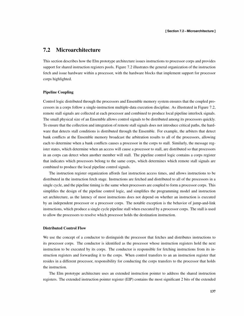
[ Section 7.2 – Microarchitecture ]
7.2 Microarchitecture
This section describes how the Elm prototype architecture issues instructions to processor corps and providessupport for shared instruction registers pools. Figure 7.2 illustrates the general organization of the instructionfetch and issue hardware within a processor, with the hardware blocks that implement support for processorcorps highlighted.
Pipeline Coupling
Control logic distributed through the processors and Ensemble memory system ensures that the coupled pro-cessors in a corps follow a single-instruction multiple-data execution discipline. As illustrated in Figure 7.2,remote stall signals are collected at each processor and combined to produce local pipeline interlock signals.The small physical size of an Ensemble allows control signals to be distributed among its processors quickly.To ensure that the collection and integration of remote stall signals does not introduce critical paths, the hard-ware that detects stall conditions is distributed through the Ensemble. For example, the arbiters that detectbank conflicts at the Ensemble memory broadcast the arbitration results to all of the processors, allowingeach to determine when a bank conflicts causes a processor in the corps to stall. Similarly, the message reg-ister states, which determine when an access will cause a processor to stall, are distributed so that processorsin an corps can detect when another member will stall. The pipeline control logic contains a corps registerthat indicates which processors belong to the same corps, which determines which remote stall signals arecombined to produce the local pipeline control signals.
The instruction register organization affords fast instruction access times, and allows instructions to bedistributed in the instruction fetch stage. Instructions are fetched and distributed to all of the processors in asingle cycle, and the pipeline timing is the same when processors are coupled to form a processor corps. Thissimplifies the design of the pipeline control logic, and simplifies the programming model and instructionset architecture, as the latency of most instructions does not depend on whether an instruction is executedby an independent processor or a processor corps. The notable exception is the behavior of jump-and-linkinstructions, which produce a single cycle pipeline stall when executed by a processor corps. The stall is usedto allow the processors to resolve which processor holds the destination instruction.
Distributed Control Flow
We use the concept of a conductor to distinguish the processor that fetches and distributes instructions toits processor corps. The conductor is identified as the processor whose instruction registers hold the nextinstruction to be executed by its corps. The conductor is responsible for fetching instructions from its in-struction registers and forwarding it to the corps. When control transfers to an an instruction register thatresides in a different processor, responsibility for conducting the corps transfers to the processor that holdsthe instruction.
The Elm prototype architecture uses an extended instruction pointer to address the shared instructionregisters. The extended instruction pointer register (EIP) contains the most significant 2 bits of the extended
137

[ Chapter 7 – Ensembles of Processors ]
remote instructions remote
instructionsEIP
0.0
0.2
InstructionRegisters
InstructionRegisters
branch target
XMU ALU
IP
+1
issue stall
DE
IF
BUPipeline ControlLogic EX
WB
ILLoad Unit
IRMUPL scoreboard
remotestall
local instructions
Figure 7.2 – Group Instruction Issue Microarchitecture. The extended instruction pointer (EIP) determineswhich processor holds the next instruction.
instruction pointer; the EIP register indicates which processor contains the shared instruction register that isaddressed by the extended instruction pointer. The instruction pointer register (IP) contains the remainder ofthe extended instruction pointer. As when processors execute independently, the IP register holds the addressof the next instruction to be fetched from the instruction register file.
In most situations, the conductor is the only member of the corps that needs to maintain a precise instruc-tion pointer. The other processors need to ensure that the contents of their EIP registers are correct so that theycan correctly identify the conductor. Only the conductor automatically updates its instruction pointer aftereach instruction is fetched. The remaining processors update their extended instruction pointers when control
138

[ Section 7.3 – Examples ]
flow instructions are encountered. Because control flow instructions encode their destination explicitly, anaccurate extended instruction pointer value is forwarded in each control flow instruction. This ensures that allof the processors have a correct extended instruction pointer immediately following a transfer of control, andit ensures that control flow instructions always produce the required transfer of responsibility for conductingthe corps.
The Elm prototype uses an inexpensive strategy for detecting when responsibility for conducting a corpsshould be transferred to a different processor. The conductor detects that control is about to transfer to adifferent processor when the hardware that updates the instruction pointer generates a carry into the extendedinstruction pointer bits. The carry signals that the extended instruction pointer addresses an instruction ina different processor. To transfer control, the conductor forwards its instruction pointer to the corps andsignals the other members of the corps to update their extended instruction pointers. The conductor stallsthe execution of the processor corps for one cycle during the transfer of control, during which the instructionforwarded by the conductor is invalid. The same strategy is used to broadcast the extended instruction pointerwhen the conductor identifies a jump-and-link operation.
We could avoid the one cycle stall by having the conductor detect that control is about to transfer one cyclebefore control actually transfers. This would require that the conductor continuously monitor the extendedinstruction pointer. The additional logic required to do so would toggle whenever the instruction pointer isupdated, and would contribute to the overhead of delivering instructions to processors regardless of whetherthey operate independently or are coupled. The additional branch delay is encountered infrequently and rarelyimpacts application performance, as software usually inserts control flow operations to explicitly transfercontrol before control reaches the last instruction in the conductor’s instruction register file.
Resolving Control Flow Destinations
As described in a previous chapter, Elm processors resolve the destination of control flow instructions thatencode their destinations as relative displacements when instructions are transferred to instruction registers.When the instruction register management unit (IRMU) transfers a control flow instruction that encodes arelative destination to the instruction registers, it resolves the destination by adding the displacement to theshared instruction register at which the instruction is loaded. The destination is stored as a shared instructionregister identifier, and the instruction is converted to an equivalent control flow instruction using a fixeddestination encoding.
7.3 Examples
This section describes how the indexed registers can be used to compose messages, and presents a parallelimplementation of a finite impulse response filter that uses message and processor corps.
139
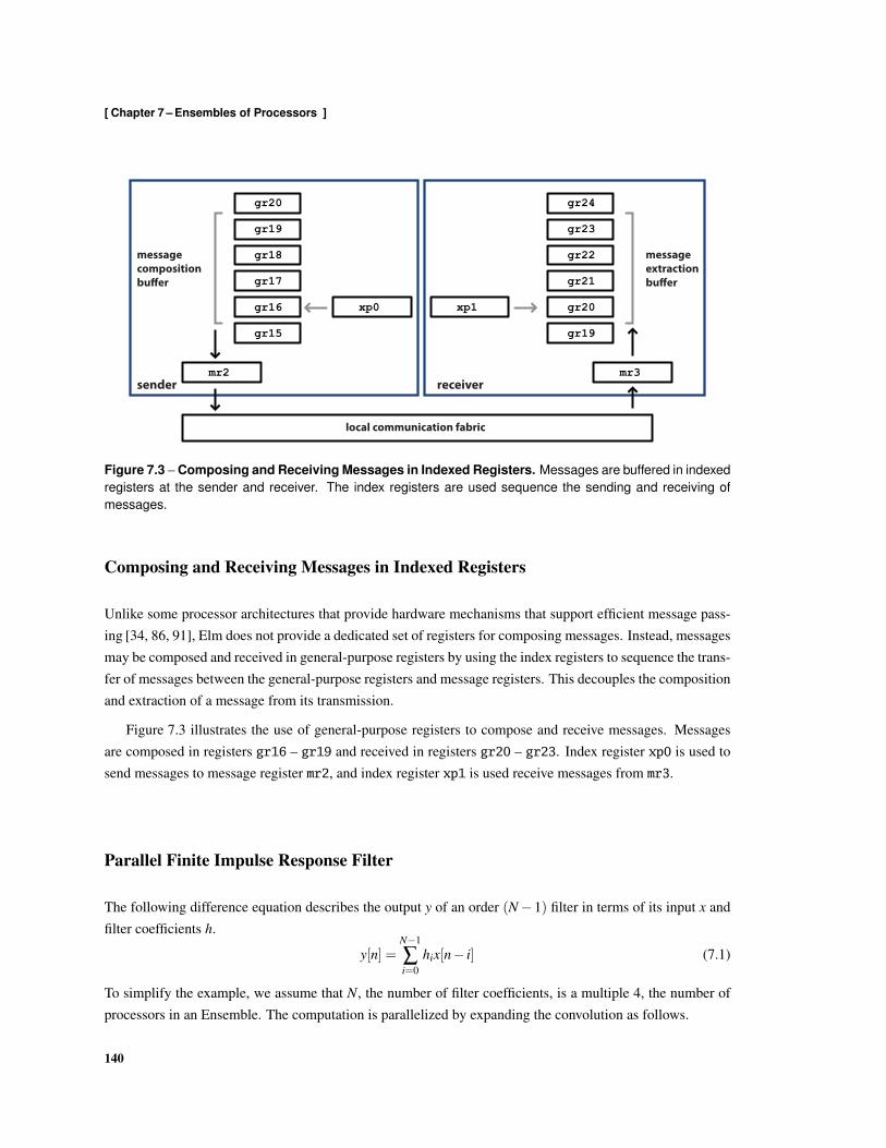
[ Chapter 7 – Ensembles of Processors ]
gr16
gr17
gr18
gr19
gr15
gr20
xp0
messagecompositionbu!er
messageextractionbu!er
sender receiver
gr20
gr21
gr22
gr23
gr19
gr24
xp1
local communication fabric
mr2 mr3
Figure 7.3 – Composing and Receiving Messages in Indexed Registers. Messages are buffered in indexedregisters at the sender and receiver. The index registers are used sequence the sending and receiving ofmessages.
Composing and Receiving Messages in Indexed Registers
Unlike some processor architectures that provide hardware mechanisms that support efficient message pass-ing [34, 86, 91], Elm does not provide a dedicated set of registers for composing messages. Instead, messagesmay be composed and received in general-purpose registers by using the index registers to sequence the trans-fer of messages between the general-purpose registers and message registers. This decouples the compositionand extraction of a message from its transmission.
Figure 7.3 illustrates the use of general-purpose registers to compose and receive messages. Messagesare composed in registers gr16 – gr19 and received in registers gr20 – gr23. Index register xp0 is used tosend messages to message register mr2, and index register xp1 is used receive messages from mr3.
Parallel Finite Impulse Response Filter
The following difference equation describes the output y of an order (N−1) filter in terms of its input x andfilter coefficients h.
y[n] =N−1
∑i=0
hix[n− i] (7.1)
To simplify the example, we assume that N, the number of filter coefficients, is a multiple 4, the number ofprocessors in an Ensemble. The computation is parallelized by expanding the convolution as follows.
140

[ Section 7.3 – Examples ]
for ( int i = 0; i < N; i++) {sum += h[i]*x[n+N-i];
}y[n] = sum;
fixed32 sum = 0;
for ( int i = p*N/P; i < (p+1)*N/P; i++) {psum[p] += h[i]*x[n+N-i];
}}
for ( int p = 0; p < P; p++ ) {psum[p] = 0;
for ( int p = 0; p < P; p++ ) {
y[n] = sum;
sum += psum[p];}
fixed32 sum = 0; fixed32 psum[P];100101102103104
200201202203204205206207208209210
Figure 7.4 – Source Code Fragment for Parallelized fir. The serial code fragment appears on the left. Theparallel code fragment appears on the right. The data-parallel for loop at line 201 is mapped to P processors.
N−1
∑i=0
hix[N− i] =N/4−1
∑i=0
hix[N− i]
+2N/4−1
∑i=N/4
hix[N− i]
+3N/4−1
∑i=2N/4
hix[N− i]
+4N/4−1
∑i=3N/4
hix[N− i] (7.2)
The computation is distributed so that each thread computes one term of the expanded summation. Thisallows the filter coefficients and samples to be distributed across multiple processors without replicating anyof the coefficients and samples.
Figure 7.5 illustrates the decomposition and mapping of the coefficients and samples to the processorsin an Ensemble. Processor EP0 receives the input sample stream in message register mr4. Processor EP3computes the final output of the filter and forwards it through message register mr5. The implementation usesindexed registers to store the filter coefficients and samples. The samples are accessed through index registerxp0 and the coefficients are accessed through index register xp1. The message registers are configured toallow samples to be forwarded through message register mr5 and received in message register mr4.
Figure 7.6 shows the assembly code fragment that implements the kernel of the finite impulse responsefilter. The code that configures the processors and loads the instruction registers are not shown to simplify andfocus the example. Basic block BB1 is executed by a processor corps comprising all four of the processors inthe Ensemble. The instructions in basic block BB1 implement the multiplications and additions that form thekernel of the filter computation. The partial sums computed by the individual processors are sent to processorEP3 at line 116, where the multiply-and-accumulate operation writes message register mr3.
Basic block BB2 is executed by all of the processors. The instructions in basic block BB2 forward samples
141
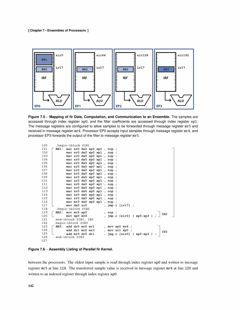
[ Chapter 7 – Ensembles of Processors ]
EP0 EP1 EP2 EP3
BB2 ir17
sir0
ALU
BB1
BB2 ir17
sir64
BB3 ir17
sir192
BB2 ir17
sir128
ALU ALU ALU
IRF IRF IRF IRF
Figure 7.5 – Mapping of fir Data, Computation, and Communication to an Ensemble. The samples areaccessed through index register xp0, and the filter coefficients are accessed through index register xp1.The message registers are configured to allow samples to be forwarded through message register mr5 andreceived in message register mr4. Processor EP0 accepts input samples through message register mr4, andprocessor EP3 forwards the output of the filter to message register mr5.
mac zr0 da0 xp0 xp1 , nop ;
mac zr0 da0 xp0 xp1 , nop ;mac zr0 da0 xp0 xp1 , nop ;mac zr0 da0 xp0 xp1 , nop ;mac zr0 da0 xp0 xp1 , nop ;mac zr0 da0 xp0 xp1 , nop ;mac mr3 da0 xp0 xp1 , nop ;
100
117
BB1:
mov mr5 xp0 , nop ;
mov da0 zr0 , jmp.i [ir17] ;
mac zr0 da0 xp0 xp1 , nop ;
mac zr0 da0 xp0 xp1 , nop ;mac zr0 da0 xp0 xp1 , nop ;mac zr0 da0 xp0 xp1 , nop ;mac zr0 da0 xp0 xp1 , nop ;
mac zr0 da0 xp0 xp1 , nop ;
mac zr0 da0 xp0 xp1 , nop ;mac zr0 da0 xp0 xp1 , nop ;mac zr0 da0 xp0 xp1 , nop ;
118
mov xp0 mr4 , jmp.c [sir0] ( ep0:ep3 ) ;119
add dr0 mr0 mr1 , mov xp0 mr4 ;add dr1 mr2 mr3 , mov zr1 xp0 ;add mr5 dr0 dr1 , jmg.c [sir0] ( ep0:ep3 ) ;
BB2:
BB3:.begin-iblock @IB3
.end-iblock @IB3
.begin-iblock @IB1
.end-iblock @IB1, IB2120121122123124125126
101102103104105106107108109110111112113114115116
.begin-iblock @IB2
127
IB2
IB3
Figure 7.6 – Assembly Listing of Parallel fir Kernel.
between the processors. The oldest input sample is read through index register xp0 and written to messageregister mr5 at line 119. The transferred sample value is received in message register mr4 at line 120 andwritten to an indexed register through index register xp0.
142

[ Section 7.4 – Allocation and Scheduling ]
EP0 EP1 EP2 EP3
IB2 ir17
sir0
ALU
IB1
IB2 ir17
sir64
IB3 ir17
sir192
IB2 ir17
sir128
ALU ALU ALU
IRF IRF IRF IRF
Figure 7.7 – Mapping of Instruction Blocks to Instruction Registers.
Basic block BB3 is executed by processor EP3. The instructions in basic block BB3 compute the output ofthe filter by combining the partial sums sent from the processors. The partial sums are received in messageregisters mr0 – mr3. The filter output is computed at line 124 and forwarded to message register mr5. Thejump as processor corps instructions at lines 120 and 126 transfer control back to basic block BB1.
Figure 7.7 shows the mapping of instruction blocks to instruction registers. The instruction blocks aremapped so that basic block BB1 resides in shared instruction registers sir0 – sir16. Basic block BB2
resides in instruction registers ir17 – ir18 in processors EP0 – EP2. Basic block BB3 resides in instructionregisters ir17 – 19 in processor EP3, and is aligned to basic block BB2. The alignment allows the jump asindependent processors instruction at line 117 to correctly transfer control when the processors decouple andresume independent execution.
Figure 7.8 illustrates the instruction fetch and instruction issue schedules for each of the processors in theEnsemble. We can calculate the number of instruction pairs issued to the processors during the execution ofone iteration of the loop as
4×17+3×2+3 = 77. (7.3)
And we can calculate the number of instructions fetched from instruction registers during the execution ofone iteration of the loop as
17+3×2+3 = 26. (7.4)
From 7.3 and 7.4, we can readily calculate that executing basic block BB1 in a processor corps reduces thenumber of instructions fetched from instruction registers by more than 66%.
7.4 Allocation and Scheduling
When applications with both data-parallel regions and thread-parallel regions are compiled, the compiler pro-duces code that contains both shared instruction blocks and private instruction blocks. Control may transfer
143
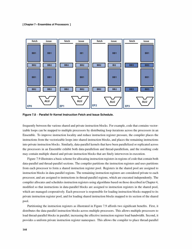
[ Chapter 7 – Ensembles of Processors ]
BB1 BB1BB1
EP0 EP1 EP2 EP3
ALU ALU ALU ALU
BB1
BB2 BB2 BB2BB2 BB2 IB2 BB3 BB3
BB2 BB2 BB2BB2 BB2 BB2 BB3 BB3
fetch issue fetch issue fetch issue fetch issue
BB1
BB1IB1BB1
BB1
BB1
Figure 7.8 – Parallel fir Kernel Instruction Fetch and Issue Schedule.
frequently between the various shared and private instruction blocks. For example, code that contains vector-izable loops can be mapped to multiple processors by distributing loop iterations across the processors in anEnsemble. To improve instruction locality and reduce instruction register pressure, the compiler places theinstructions from the vectorizable loops into shared instruction blocks, and places the remaining instructionsinto private instruction blocks. Similarly, data-parallel kernels that have been parallelized or replicated acrossthe processors in an Ensemble exhibit both data-parallelism and thread-parallelism, and the resulting codemay contain multiple shared and private instruction blocks that are finely interwoven in execution.
Figure 7.9 illustrates a basic scheme for allocating instruction registers in regions of code that contain bothdata-parallel and thread-parallel sections. The compiler partitions the instruction registers and uses partitionsfrom each processor to form a shared instruction register pool. Registers in the shared pool are assigned toinstruction blocks in data-parallel regions. The remaining instruction registers are considered private to eachprocessor, and are assigned to instructions in thread-parallel regions, which are executed independently. Thecompiler allocates and schedules instruction registers using algorithms based on those described in Chapter 4,modified so that instructions in data-parallel blocks are assigned to instruction registers in the shared pool,which are managed cooperatively. Each processor is responsible for loading instruction blocks mapped to itsprivate instruction register pool, and for loading shared instruction blocks mapped to its section of the sharedpool.
Partitioning the instruction registers as illustrated in Figure 7.9 affords two significant benefits. First, itdistributes the data-parallel instruction blocks across multiple processors. This allows multiple processors toload thread-parallel blocks in parallel, increasing the effective instruction register load bandwidth. Second, itprovides a uniform private instruction register namespace. This allows the compiler to place thread-parallel
144

[ Section 7.5 – Allocation and Scheduling ]
EP0 EP1 EP2 EP3
Shared InstructionRegisters
PrivateInstructionRegisters
Figure 7.9 – Shared Instruction Register Allocation. The compiler partitions the instruction register filesand combines aligned partitions from each processor to form a shared instruction register pool. The remaininginstruction registers are private to each processor, and are available for instructions that are executed inde-pendently. Instruction blocks that are targets of control flow instructions that cause the processors to decoupleare aligned in the private instruction register partitions. Illustrated as arrows in the figure, the compiler insertsjump instructions to transfer control between shared instruction blocks that reside in different processors.
instruction blocks at common addresses within each local private partition. As described subsequently, thissimplifies code generation and improves performance.
When the instruction registers are partitioned as shown in Figure 7.9, the mapping of local instructionregister identifiers to shared instruction register identifiers results in the private instruction registers partition-ing the pool of shared instruction registers into 4 sets. The mapping of local identifiers to shared identifiers isdescribed in detail in Appendix C. The shared registers within each processor reside at contiguous addresses,but the sets of private instruction registers are mapped to addresses between the shared register sets. The logi-cal organization of the shared registers is illustrated in Figure 7.9. When necessary, the compiler constructs acontiguous pool of shared registers using control flow instructions to stitch together the registers in differentregister files. This allows the compiler to reason about the shared instruction register pool as a single contigu-ous block of registers. When an instruction block spans multiple register files, the compiler inserts explicitcontrol flow instructions to transfer control between the shared registers in different instruction register files.
The compiler attempts to place instruction blocks so that those thread-parallel blocks that are successorsof data-parallel blocks in the control flow graph are aligned at common locations in the private partitions.This allows control flow instructions that transfer control from data-parallel blocks to thread-parallel blocksto use a common destination register location to transfer control to blocks in the local private partitions. Thisallows the compiler to use control flow instructions that are resolved early in the pipeline to transfer control.When the compiler cannot align the destination blocks, the compiler inserts a register-indirect control transfer.Aligning the blocks improves performance and efficiency because control flow instructions that are resolvedearly in the pipeline impose smaller performance penalties.
145
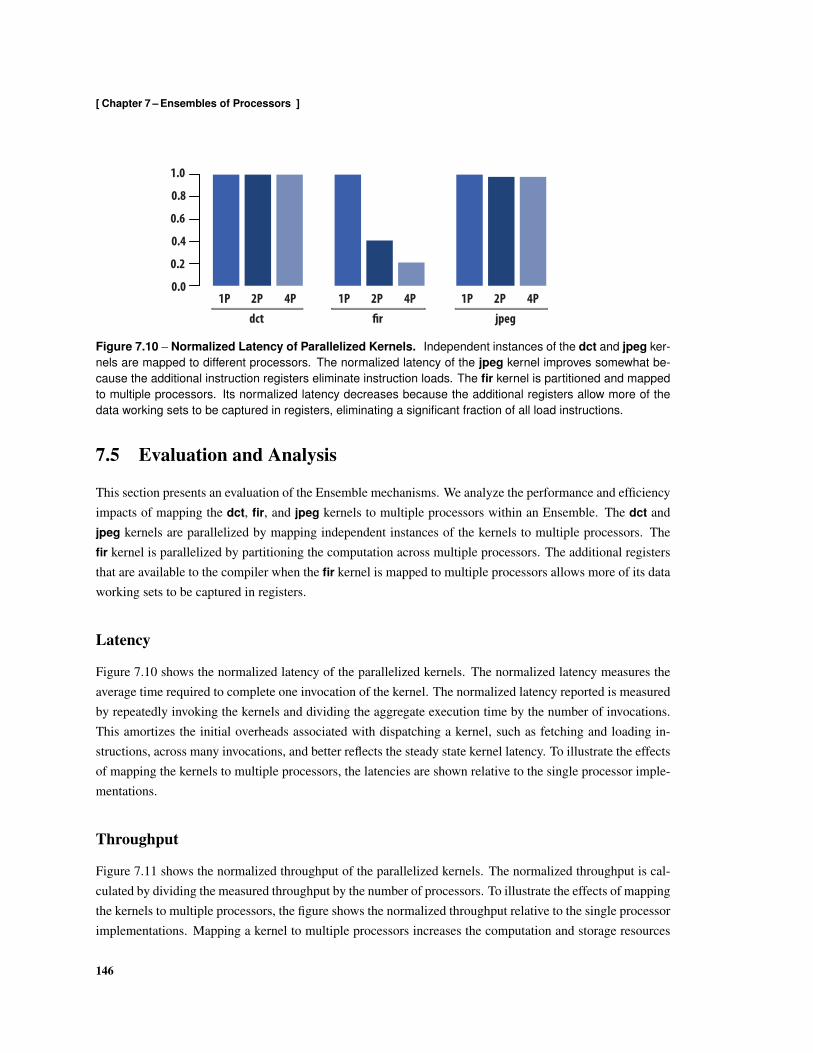
[ Chapter 7 – Ensembles of Processors ]
0.0
0.4
0.8
0.2
1.0
0.6
dct1P 2P 4P
!r1P 2P 4P
jpeg1P 2P 4P
Figure 7.10 – Normalized Latency of Parallelized Kernels. Independent instances of the dct and jpeg ker-nels are mapped to different processors. The normalized latency of the jpeg kernel improves somewhat be-cause the additional instruction registers eliminate instruction loads. The fir kernel is partitioned and mappedto multiple processors. Its normalized latency decreases because the additional registers allow more of thedata working sets to be captured in registers, eliminating a significant fraction of all load instructions.
7.5 Evaluation and Analysis
This section presents an evaluation of the Ensemble mechanisms. We analyze the performance and efficiencyimpacts of mapping the dct, fir, and jpeg kernels to multiple processors within an Ensemble. The dct andjpeg kernels are parallelized by mapping independent instances of the kernels to multiple processors. Thefir kernel is parallelized by partitioning the computation across multiple processors. The additional registersthat are available to the compiler when the fir kernel is mapped to multiple processors allows more of its dataworking sets to be captured in registers.
Latency
Figure 7.10 shows the normalized latency of the parallelized kernels. The normalized latency measures theaverage time required to complete one invocation of the kernel. The normalized latency reported is measuredby repeatedly invoking the kernels and dividing the aggregate execution time by the number of invocations.This amortizes the initial overheads associated with dispatching a kernel, such as fetching and loading in-structions, across many invocations, and better reflects the steady state kernel latency. To illustrate the effectsof mapping the kernels to multiple processors, the latencies are shown relative to the single processor imple-mentations.
Throughput
Figure 7.11 shows the normalized throughput of the parallelized kernels. The normalized throughput is cal-culated by dividing the measured throughput by the number of processors. To illustrate the effects of mappingthe kernels to multiple processors, the figure shows the normalized throughput relative to the single processorimplementations. Mapping a kernel to multiple processors increases the computation and storage resources
146
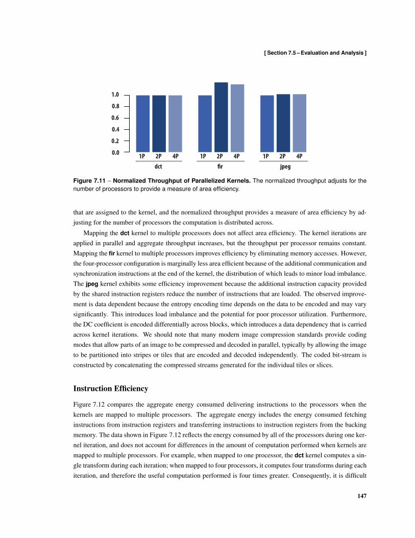
[ Section 7.5 – Evaluation and Analysis ]
0.0
0.4
0.8
0.2
1.0
0.6
dct1P 2P 4P
!r1P 2P 4P
jpeg1P 2P 4P
Figure 7.11 – Normalized Throughput of Parallelized Kernels. The normalized throughput adjusts for thenumber of processors to provide a measure of area efficiency.
that are assigned to the kernel, and the normalized throughput provides a measure of area efficiency by ad-justing for the number of processors the computation is distributed across.
Mapping the dct kernel to multiple processors does not affect area efficiency. The kernel iterations areapplied in parallel and aggregate throughput increases, but the throughput per processor remains constant.Mapping the fir kernel to multiple processors improves efficiency by eliminating memory accesses. However,the four-processor configuration is marginally less area efficient because of the additional communication andsynchronization instructions at the end of the kernel, the distribution of which leads to minor load imbalance.The jpeg kernel exhibits some efficiency improvement because the additional instruction capacity providedby the shared instruction registers reduce the number of instructions that are loaded. The observed improve-ment is data dependent because the entropy encoding time depends on the data to be encoded and may varysignificantly. This introduces load imbalance and the potential for poor processor utilization. Furthermore,the DC coefficient is encoded differentially across blocks, which introduces a data dependency that is carriedacross kernel iterations. We should note that many modern image compression standards provide codingmodes that allow parts of an image to be compressed and decoded in parallel, typically by allowing the imageto be partitioned into stripes or tiles that are encoded and decoded independently. The coded bit-stream isconstructed by concatenating the compressed streams generated for the individual tiles or slices.
Instruction Efficiency
Figure 7.12 compares the aggregate energy consumed delivering instructions to the processors when thekernels are mapped to multiple processors. The aggregate energy includes the energy consumed fetchinginstructions from instruction registers and transferring instructions to instruction registers from the backingmemory. The data shown in Figure 7.12 reflects the energy consumed by all of the processors during one ker-nel iteration, and does not account for differences in the amount of computation performed when kernels aremapped to multiple processors. For example, when mapped to one processor, the dct kernel computes a sin-gle transform during each iteration; when mapped to four processors, it computes four transforms during eachiteration, and therefore the useful computation performed is four times greater. Consequently, it is difficult
147

[ Chapter 7 – Ensembles of Processors ]
0.0
0.4
0.8
0.2
1.0
0.6
dct1P 2P 4P
!r1P 2P 4P
jpeg1P 2P 4P
Figure 7.12 – Aggregate Instruction Energy. The aggregate instruction energy measures the total energyconsumed delivering instructions to the processors. The data have been normalized within each kernel toillustrate trends.
0.0
0.4
0.8
0.2
1.0
0.6
dct1P 2P 4P
!r1P 2P 4P
jpeg1P 2P 4P
Figure 7.13 – Normalized Instruction Energy. The normalized instruction measures the ratio of the energyconsumed delivering instructions to the number of processors, and provides a measure of energy efficiency.
to infer too much from Figure 7.12 about the efficiency of using processor corps to map kernels to multipleprocessors. However, the data shown in Figure 7.12 provides insights into how efficiency is improved and ex-poses limitations. The data for the dct kernel show that energy consumed distributing instructions to multipleprocessors is comparable to the energy consumed accessing instructions stored in local instruction registers.This illustrates how the effectiveness of using SIMD execution to amortize instruction supply energy is lim-ited by the cost of distributing instructions, and how inexpensive local instruction stores reduce some of theefficiency advantages of SIMD execution. The data also illustrate that the significant improvement in the effi-ciency of the fir kernel results because fewer instructions are executed when the kernel is mapped to multipleprocessors; the reduction in the number of instructions executed is more than sufficient to compensate forthe additional energy consumed distributing instructions to multiple processors. Figure 7.13 shows the nor-malized instruction energy, calculated by dividing the aggregate instruction energy by the amount of usefulcomputation completed, which provides a direct measure of energy efficiency.
The dct kernel exposes limits to the improvement in efficiency that are achieved by distributing instruc-tions to multiple processors. The aggregate instruction energy of the dct kernel is dominated by the fetchingof instructions from instruction registers and the distributing of them among the processors comprising a
148
[ Section 7.6 – Related Work ]
processor corps. Each processor has enough instruction registers to capture both kernels entirely, so theadditional instruction register capacity provided by the shared instruction register pool does not reduce thenumber of instructions that are transferred to the instruction register files. Furthermore, the initial cost ofloading instructions when the kernels is launched is negligible when amortized across many kernel iterations.
The increase in the aggregate instruction energy observed when the dct kernel is mapped to more proces-sors exposes the expense of transferring instructions to remote processors. Interconnect capacitance increaseswith the physical distance instructions traverse, and the energy expended distributing instructions increaseswith the capacitance that is switched when instructions are delivered to remote processors. Thus, though thenumber of instruction register accesses remains constant, the loss of physical locality increases the cost ofdelivering instructions. As Figure 7.12 illustrates, even local communication can require a significant expen-diture of energy, and improvements in energy efficiency are limited by the loss of physical locality. However,less energy is required to transfer instructions to remote processors than is required for additional processorsto fetch instructions from their local instruction registers, and modest efficiency improves are realized whenthe kernel is mapped to a processor corps, as Figure 7.13 shows.
The effectiveness of exchanging instruction locality for fewer instruction store accesses depends on therelative cost of distributing instructions and accessing local instructions. These costs can vary significantlyacross different architectures. For example, accessing an instruction cache consumes more energy than ac-cessing an instruction register file. Consequently, processors that fetch instructions from instruction cacheswill benefit more from architectures that allow instructions to be issued to multiple processors.
Like the dct kernel, the aggregate instruction energy of the fir kernel is dominated by the fetching ofinstructions from instruction registers and the distributing of them among the processors comprising a pro-cessor corps. There are enough instruction registers to accommodate the kernel, and the initial cost of loadinginstructions when the kernel is launched is negligible when amortized across many kernel iterations. Thenormalized instruction energy for the fir decreases because fewer instructions are executed. The additionalindexed registers accommodate more of the working sets, and fewer memory operations are performed.
The normalized instruction energy for the jpeg kernel is more informative because the instruction reg-isters lack sufficient capacity to capture instruction reuse across subsequent invocations of the kernel. TheDCT transform component is performed in parallel, and the instructions in the shared instruction block areread once, amortizing the memory access across multiple processors. The Huffman encoding component isexecuted by the processors independently. The initial instruction block is loaded and distributed to all of theprocessors, after which the instruction loads diverge as the processors follow different control paths. In con-trast with the dct kernel, which does not load instructions during each iteration, the jpeg kernel demonstratesboth the effectiveness of amortizing instruction issue as well as instruction loads by executing code.
7.6 Related Work
The INMOS transputer architecture [149] allows machines of different scales to be constructed as collectionsof many small, simple processing elements connected by point-to-point links. The architecture reflects adecentralized model of computation in which concurrent processes operate exclusively on local data and
149
[ Chapter 7 – Ensembles of Processors ]
communicate by passing messages on point-to-point channels. The transputers implement a stack-based load-store architecture that is capable of executing a small number of instructions. Like the HEP multiprocessordescribed subsequently, each processing element can execute multiple processes concurrently. Channels thatconnect processes executing on the same transputer are implemented as single words in memory. Channelsthat connect processes executing on different transputers are implemented by point-to-point links. In thisrespect, the programming model mirrors the physical machine design. The restriction that all communicationbe mapped to point-to-point channels complicates the task of mapping applications to a transputer. Earlytransputer implementations used a synchronous message passing protocol that required that both the sendingprocess and receiving process are ready to communicate before a message can be transferred, which limitsthe machine’s ability to overlap computation and communication.
The HEP multiprocessor system uses multithreading to hide memory latency and allows cooperatingconcurrent threads to communicate through shared registers and memory [134]. The system supports fine-grained communication and synchronization by associating an access state with every register memory anddata memory location to record whether a word is full, empty, or reserved. Load instructions can be deferreduntil the addressed data word is full, and can atomically load the data and mark the location as empty.Store instructions can be deferred until the addressed word is empty, and can atomically store the data tothe addressed memory location and mark the location as full. An instruction that accesses register memorycan be deferred until all of its operand register locations are marked full and its destination register locationis marked empty; when the instruction executes, it atomically marks its operand registers as empty and itsdestination register as full. To enforce atomicity, the destination register location is temporarily marked asreserved during the execution of the instruction, and other instructions may not execute if any of their registersare marked reserved. Multiprocessor data flow architectures use similar full-empty bit mechanisms to detectwhen the operands to an operation have been computed [113], which is fundamental to implementing theunderlying model of computation on data flow machines [9].
The MIT Alewife machine implements full-empty bit synchronization using a similar scheme to improvesupport for fine-grain parallel computation and communication through shared memory [4]. The architectureassociates a synchronization bit with each memory word. The synchronization bits are accessed throughdistinguished load and store operations that perform a test-and-set operation in parallel with the memoryaccess. The architecture allows memory operations to signal a synchronization exception when the test-and-set operation fails [3]. The original state of the synchronization bit is returned in the coprocessor status wordwhen the memory operation completes, and special branch instructions are implemented to allow software toexamine the synchronization bit.
The MIT Raw microprocessor [137] exposes a scalar operand network [138] that allows software to ex-plicitly route operands between distributed function units and register files. The distributed function unitsand register files in Raw are organized as scalar processors, and Raw’s scalar operand network effectivelyallows software to compose and receive messages in registers to reduce the latency of sending and receivingmessages comprising single scalar operands. This allows instructions from a single thread to be distributedacross multiple execution units. Scalar operand networks provide a general abstraction for exposing inter-connect to software, with the intention that exposing interconnect delays and allowing software to explicitly
150

[ Section 7.6 – Related Work ]
manage interconnect resources will allow software to schedule operations to hide communication latenciesbetween distributed function units and register files.
Vector-thread architectures allow independent threads to execute on the vector lanes [88]. This allows dataparallel codes that are not vectorizable to be mapped efficiently to the virtual processors of a vector-threadmachine, and allows the vector lanes to be used to execute arbitrary independent threads. Vector lane thread-ing allows independent threads to execute on the lanes of a multi-lane vector processor [120]. This improveslane utilization during applications phases that exhibit insufficient data-level parallelism to fully utilize theparallel vector lanes. By decoupling hardware intended for single-instruction multiple-data execution, bothvector-thread processors and vector processors that support vector-lane threading are able to use the samehardware to exploit both single-instruction multiple-data parallelism and thread-level parallelism.
The vector-thread abstract machine model connects virtual processors using a unidirectional scalar operandring network [88]. The network allows an instruction that executes on virtual processor n to transfer data di-rectly to an instruction that executes on virtual processor n + 1. Though communication between virtualprocessors is restricted, these cross virtual processor transfers allow loops with cross-iteration dependen-cies to be mapped onto the vector lanes. The execution cluster organization used in the Scale vector-threadprocessor uses queues to decouple the send and receive operations that execute on different clusters [89].
The Multiflow Trace/500 machine implements multiple function unit clusters and uses distributed localinstruction caches [24]. Machines may be configured with two coupled VLIW processors, each with 14function units, that execute a common instruction stream. The two processors appear to software as a singleVLIW processor with twice the number of function units.
The variable-instruction multiple-data (XIMD) architecture [151] extends conventional very-long instruc-tion word (VLIW) architectures [42] by associating independent instruction sequencers with each functionunit, which allows a XIMD processor to execute multiple instruction streams in parallel. Distributed con-dition code bits and synchronization bits are used to control the instruction sequencers. The sequencersand distributed synchronization bits allow a XIMD machine to implement barrier synchronization opera-tions that support medium-grain parallelism. The independent sequences and mechanisms that support inter-function unit synchronization allow for some control flow dependencies to be resolved dynamically. Thisallows a XIMD machine to emulate a tightly-coupled multiple-instruction multiple-data (MIMD) machine.As with traditional VLIW architectures, function units communicate through a global register file. LikeVLIW machines, XIMD machines require sophisticated compilers to identify and exploit instruction-levelparallelism. In addition, many of the architectural mechanisms that distinguish XIMD machines require so-phisticated compiler technology to distribute and schedule instructions from multiple loop iterations acrossthe distributed function units [111].
The distributed VLIW (DVLIW) architecture [155] extends a clustered VLIW architecture with dis-tributed instruction fetch and decode logic. Each cluster has its own program counter and local distributedinstruction cache, which enables distributed instruction sequencing. Operations that execute on different clus-ters are stored in the distributed instruction caches, similar to how instructions are stored in early horizontallymicrocoded machines [142]. Later extensions proposed coupling processors to support both instruction-leveland thread-level parallelism [156]. The resulting architecture is similar to the MIT Raw microprocessor,
151

[ Chapter 7 – Ensembles of Processors ]
except that it uses a few large VLIW cores rather than many small RISC cores. As with Raw, cores are con-nected by a scalar operand network. The network is accessed through dedicated communication units that areexposed to software. The instruction set supports both direct scalar operand puts and gets between adjacentcores, and decoupled sends and receives between all cores. Data transferred using sends and receives traverseinter-cluster decoupling queues. The compiler statically schedules instructions to exploit instruction-levelparallelism within a core. A single thread may be scheduled across multiple cores using gets and puts tosynthesize inter-cluster moves in a traditional clustered VLIW machine, or multiple threads may be sched-uled across the cores. The architecture requires a memory system that supports transactional coherence andconsistency [62] to dynamically resolve memory dependencies, which significantly complicates the designand implementation of the memory system.
7.7 Chapter Summary
Ensembles allow software to use collections of coupled processors to exploit data-level and task-level par-allelism efficiently. The Ensemble organization supports the concept of processor corps, collections of pro-cessors that execute a common instruction stream. This allows processors to pool their instruction registers,and thereby increase the aggregate register capacity that is available to the corps. The instruction registerorganization improves the effectiveness of the processor corps concept by allowing software to control theplacement of shared and private instructions throughout the Ensemble.
152
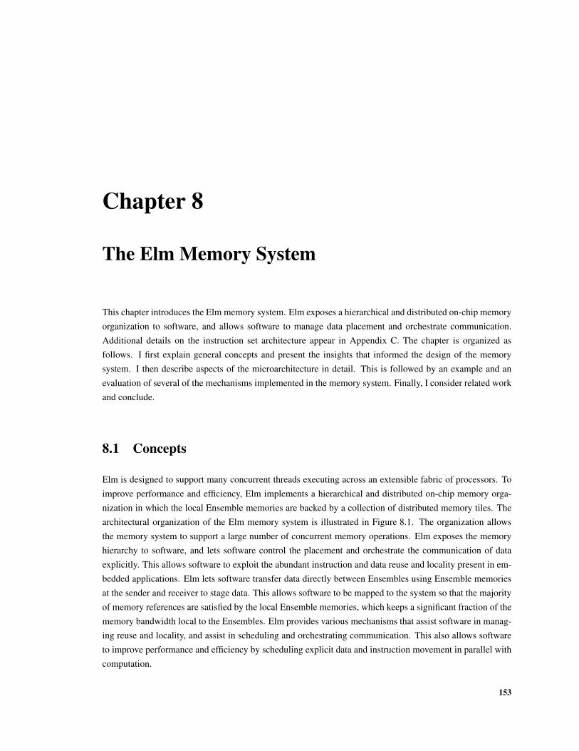
Chapter 8
The Elm Memory System
This chapter introduces the Elm memory system. Elm exposes a hierarchical and distributed on-chip memoryorganization to software, and allows software to manage data placement and orchestrate communication.Additional details on the instruction set architecture appear in Appendix C. The chapter is organized asfollows. I first explain general concepts and present the insights that informed the design of the memorysystem. I then describe aspects of the microarchitecture in detail. This is followed by an example and anevaluation of several of the mechanisms implemented in the memory system. Finally, I consider related workand conclude.
8.1 Concepts
Elm is designed to support many concurrent threads executing across an extensible fabric of processors. Toimprove performance and efficiency, Elm implements a hierarchical and distributed on-chip memory orga-nization in which the local Ensemble memories are backed by a collection of distributed memory tiles. Thearchitectural organization of the Elm memory system is illustrated in Figure 8.1. The organization allowsthe memory system to support a large number of concurrent memory operations. Elm exposes the memoryhierarchy to software, and lets software control the placement and orchestrate the communication of dataexplicitly. This allows software to exploit the abundant instruction and data reuse and locality present in em-bedded applications. Elm lets software transfer data directly between Ensembles using Ensemble memoriesat the sender and receiver to stage data. This allows software to be mapped to the system so that the majorityof memory references are satisfied by the local Ensemble memories, which keeps a significant fraction of thememory bandwidth local to the Ensembles. Elm provides various mechanisms that assist software in manag-ing reuse and locality, and assist in scheduling and orchestrating communication. This also allows softwareto improve performance and efficiency by scheduling explicit data and instruction movement in parallel withcomputation.
153

[ Chapter 8 – The Elm Memory System ]
DRAM
Interconnection Network
MCTRL
DRAM
MCTRL
Distributed Memory
EnsembleMemory
SystemMemory
Ensemble
Memory Tile
[ Elm chip boundary ]
Figure 8.1 – Elm Memory Hierarchy. The memory hierarchy is composed of Ensemble memories, distributedmemories, and off-chip system memory. The system memory is accessed through memory controllers (MC-TRL). The Ensemble memories are used to stage instruction and data transfers to Ensemble processors, andto capture small working sets locally. The distributed memories are used to capture larger instruction and dataworking sets, to stage instruction and data transfers up and down the memory hierarchy, and to stage datatransfers between Ensembles.
154
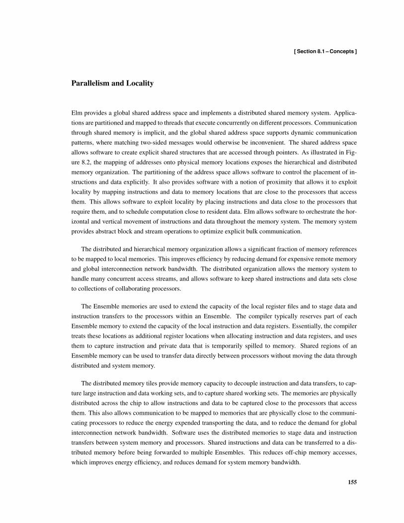
[ Section 8.1 – Concepts ]
Parallelism and Locality
Elm provides a global shared address space and implements a distributed shared memory system. Applica-tions are partitioned and mapped to threads that execute concurrently on different processors. Communicationthrough shared memory is implicit, and the global shared address space supports dynamic communicationpatterns, where matching two-sided messages would otherwise be inconvenient. The shared address spaceallows software to create explicit shared structures that are accessed through pointers. As illustrated in Fig-ure 8.2, the mapping of addresses onto physical memory locations exposes the hierarchical and distributedmemory organization. The partitioning of the address space allows software to control the placement of in-structions and data explicitly. It also provides software with a notion of proximity that allows it to exploitlocality by mapping instructions and data to memory locations that are close to the processors that accessthem. This allows software to exploit locality by placing instructions and data close to the processors thatrequire them, and to schedule computation close to resident data. Elm allows software to orchestrate the hor-izontal and vertical movement of instructions and data throughout the memory system. The memory systemprovides abstract block and stream operations to optimize explicit bulk communication.
The distributed and hierarchical memory organization allows a significant fraction of memory referencesto be mapped to local memories. This improves efficiency by reducing demand for expensive remote memoryand global interconnection network bandwidth. The distributed organization allows the memory system tohandle many concurrent access streams, and allows software to keep shared instructions and data sets closeto collections of collaborating processors.
The Ensemble memories are used to extend the capacity of the local register files and to stage data andinstruction transfers to the processors within an Ensemble. The compiler typically reserves part of eachEnsemble memory to extend the capacity of the local instruction and data registers. Essentially, the compilertreats these locations as additional register locations when allocating instruction and data registers, and usesthem to capture instruction and private data that is temporarily spilled to memory. Shared regions of anEnsemble memory can be used to transfer data directly between processors without moving the data throughdistributed and system memory.
The distributed memory tiles provide memory capacity to decouple instruction and data transfers, to cap-ture large instruction and data working sets, and to capture shared working sets. The memories are physicallydistributed across the chip to allow instructions and data to be captured close to the processors that accessthem. This also allows communication to be mapped to memories that are physically close to the communi-cating processors to reduce the energy expended transporting the data, and to reduce the demand for globalinterconnection network bandwidth. Software uses the distributed memories to stage data and instructiontransfers between system memory and processors. Shared instructions and data can be transferred to a dis-tributed memory before being forwarded to multiple Ensembles. This reduces off-chip memory accesses,which improves energy efficiency, and reduces demand for system memory bandwidth.
155
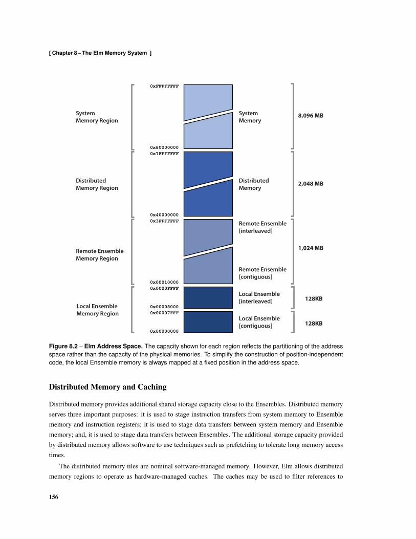
[ Chapter 8 – The Elm Memory System ]
Local Ensemble[interleaved]
Local Ensemble [contiguous]
Remote Ensemble[interleaved]
Remote Ensemble[contiguous]
Distributed Memory
System Memory
0x00000000
0x00007FFF0x00008000
0x0000FFFF
128KB
128KB
0x00010000
0x3FFFFFFF
0x800000000x7FFFFFFF
0x40000000
0xFFFFFFFF
1,024 MB
2,048 MB
8,096 MBSystem Memory Region
DistributedMemory Region
Remote EnsembleMemory Region
Local EnsembleMemory Region
Figure 8.2 – Elm Address Space. The capacity shown for each region reflects the partitioning of the addressspace rather than the capacity of the physical memories. To simplify the construction of position-independentcode, the local Ensemble memory is always mapped at a fixed position in the address space.
Distributed Memory and Caching
Distributed memory provides additional shared storage capacity close to the Ensembles. Distributed memoryserves three important purposes: it is used to stage instruction transfers from system memory to Ensemblememory and instruction registers; it is used to stage data transfers between system memory and Ensemblememory; and, it is used to stage data transfers between Ensembles. The additional storage capacity providedby distributed memory allows software to use techniques such as prefetching to tolerate long memory accesstimes.
The distributed memory tiles are nominal software-managed memory. However, Elm allows distributedmemory regions to operate as hardware-managed caches. The caches may be used to filter references to
156

[ Section 8.1 – Concepts ]
system, distributed, and remote Ensemble memory. Software-managed distributed memory allows softwareto coordinate reuse and locality, and to orchestrate the movement of data through the memory hierarchyexplicitly. This improves efficiency and predictability when mapping software that is amenable to staticanalysis. Caches assist software in managing reuse and locality when access patterns and data placement aredifficult or impossible to determine using static analyses. The caches can also be used to filter referencesto shared objects that are mapped to system memory, which keeps more memory bandwidth closer to theprocessors. This improves efficiency by keeping more communication close to the processors and reducingaccesses to more expensive system and remote memory.
Caches soften the process of mapping applications to Elm. The caches exploit locality using conventionalload and store memory operations. They also provide a reasonable way to capture instruction blocks close toprocessors without the complexity of using Ensemble memory to store both instructions and data.
Elm does not implement hardware cache coherence. Instead, software may be constructed to ensure thatany cached copies of shared data that may be updated are cached at a common location on the chip, or mayexplicitly invalidate cached copies of shared data. Elm provides efficient synchronization mechanisms thatsoftware may use to coordinate the invalidating of cached copies of shared data.
Software-Constructed Cache Hierarchies
The caches in Elm are software-allocated and hardware-managed. Software designates parts of the distributedmemory tiles to operate as caches, and determines which regions of memory are accessed through the caches.Elm allows software to control the mappings from cached addresses to the distributed memory tiles that cachethe addresses. This allows software to construct cache hierarchies, which affords software significant controlover where instructions and data are cached, and when multiple cached copies of instructions and data mayexist. The flexibility lets software map overlapping working sets to shared caches, which improves cacheutilization and reduces memory bandwidth demand.
Elm associates a small cached address translation table with each processor and each distributed memorytile to record the mappings from cached addresses to cache controllers. Each entry describes a contiguousregion of the address space and associates a distributed memory tile or system memory controller with theregion. The mapping may restrict the ways of the cache that are used to cache the data, which effectivelyallows software to partition cache resources within a memory tile. When a memory controller handles acached memory operation, it uses its local cached address translation tables to determine where the operationshould be forwarded to when a request cannot be handled locally. The tables are small, and typically provide4 entries.
The cached address translation tables provide a simple mechanism that allows software to partition cachecapacity and to isolate access streams. For example, software may use one distributed memory tile to cacheaddresses that contain instructions, and a different memory tile to cache addresses that contain data. Thisisolates the instruction and data streams and keeps them from displacing each other in the caches. To improvelocality, software may configure the translation tables so that distant processors use local tiles to distributecached copies of shared instructions and read-only data. Similarly, to distribute memory references and
157
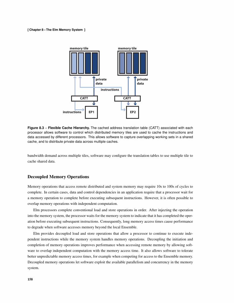
[ Chapter 8 – The Elm Memory System ]
EP1 EP2
CATT
instructions
privatedata
CATT
instructions
private data
memory tile memory tile
Figure 8.3 – Flexible Cache Hierarchy. The cached address translation table (CATT) associated with eachprocessor allows software to control which distributed memory tiles are used to cache the instructions anddata accessed by different processors. This allows software to capture overlapping working sets in a sharedcache, and to distribute private data across multiple caches.
bandwidth demand across multiple tiles, software may configure the translation tables to use multiple tile tocache shared data.
Decoupled Memory Operations
Memory operations that access remote distributed and system memory may require 10s to 100s of cycles tocomplete. In certain cases, data and control dependencies in an application require that a processor wait fora memory operation to complete before executing subsequent instructions. However, it is often possible tooverlap memory operations with independent computation.
Elm processors complete conventional load and store operations in order. After injecting the operationinto the memory system, the processor waits for the memory system to indicate that it has completed the oper-ation before executing subsequent instructions. Consequently, long memory access times cause performanceto degrade when software accesses memory beyond the local Ensemble.
Elm provides decoupled load and store operations that allow a processor to continue to execute inde-pendent instructions while the memory system handles memory operations. Decoupling the initiation andcompletion of memory operations improves performance when accessing remote memory by allowing soft-ware to overlap independent computation with the memory access time. It also allows software to toleratebetter unpredictable memory access times, for example when competing for access to the Ensemble memory.Decoupled memory operations let software exploit the available parallelism and concurrency in the memorysystem.
158
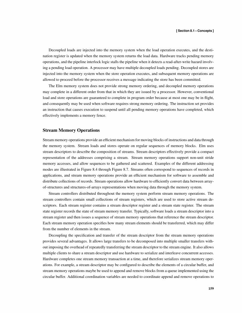
[ Section 8.1 – Concepts ]
Decoupled loads are injected into the memory system when the load operation executes, and the desti-nation register is updated when the memory system returns the load data. Hardware tracks pending memoryoperations, and the pipeline interlock logic stalls the pipeline when it detects a read-after-write hazard involv-ing a pending load operation. A processor may have multiple decoupled loads pending. Decoupled stores areinjected into the memory system when the store operation executes, and subsequent memory operations areallowed to proceed before the processor receives a message indicating the store has been committed.
The Elm memory system does not provide strong memory ordering, and decoupled memory operationsmay complete in a different order from that in which they are issued by a processor. However, conventionalload and store operations are guaranteed to complete in program order because at most one may be in flight,and consequently may be used when software requires strong memory ordering. The instruction set providesan instruction that causes execution to suspend until all pending memory operations have completed, whicheffectively implements a memory fence.
Stream Memory Operations
Stream memory operations provide an efficient mechanism for moving blocks of instructions and data throughthe memory system. Stream loads and stores operate on regular sequences of memory blocks. Elm usesstream descriptors to describe the composition of streams. Stream descriptors effectively provide a compactrepresentation of the addresses comprising a stream. Stream memory operations support non-unit stridememory accesses, and allow sequences to be gathered and scattered. Examples of the different addressingmodes are illustrated in Figure 8.4 through Figure 8.7. Streams often correspond to sequences of records inapplications, and stream memory operations provide an efficient mechanism for software to assemble anddistribute collections of records. Stream operations allow hardware to efficiently convert data between array-of-structures and structures-of-arrays representations when moving data through the memory system.
Stream controllers distributed throughout the memory system perform stream memory operations. Thestream controllers contain small collections of stream registers, which are used to store active stream de-scriptors. Each stream register contains a stream descriptor register and a stream state register. The streamstate register records the state of stream memory transfer. Typically, software loads a stream descriptor into astream register and then issues a sequence of stream memory operations that reference the stream descriptor.Each stream memory operation specifies how many stream elements should be transferred, which may differfrom the number of elements in the stream.
Decoupling the specification and transfer of the stream descriptor from the stream memory operationsprovides several advantages. It allows large transfers to be decomposed into multiple smaller transfers with-out imposing the overhead of repeatedly transferring the stream descriptor to the stream engine. It also allowsmultiple clients to share a stream descriptor and use hardware to serialize and interleave concurrent accesses.Hardware completes one stream memory transaction at a time, and therefore serializes stream memory oper-ations. For example, a stream descriptor may be configured to describe the elements of a circular buffer, andstream memory operations maybe be used to append and remove blocks from a queue implemented using thecircular buffer. Additional coordination variables are needed to coordinate append and remove operations to
159
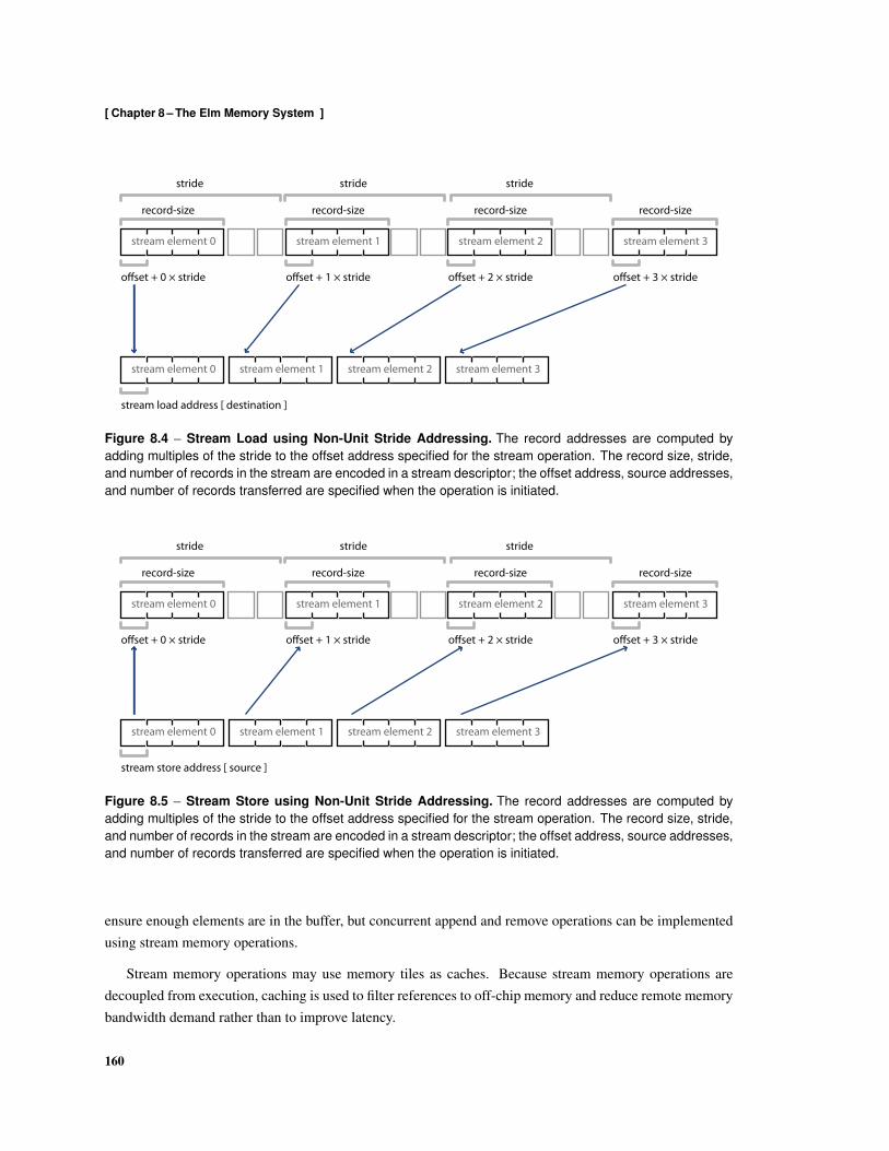
[ Chapter 8 – The Elm Memory System ]
record-size
stride
record-size
o!set + 0 " stride o!set + 1 " stride
stream element 0 stream element 1
stream element 0 stream element 1
record-size
o!set + 2 " stride
stream element 2
stream element 2
stream load address [ destination ]
record-size
o!set + 3 " stride
stream element 3
stream element 3
stride stride
Figure 8.4 – Stream Load using Non-Unit Stride Addressing. The record addresses are computed byadding multiples of the stride to the offset address specified for the stream operation. The record size, stride,and number of records in the stream are encoded in a stream descriptor; the offset address, source addresses,and number of records transferred are specified when the operation is initiated.
record-size
stride
record-size
o!set + 0 " stride o!set + 1 " stride
stream element 0 stream element 1
stream element 0 stream element 1
record-size
o!set + 2 " stride
stream element 2
stream element 2
stream store address [ source ]
record-size
o!set + 3 " stride
stream element 3
stream element 3
stride stride
Figure 8.5 – Stream Store using Non-Unit Stride Addressing. The record addresses are computed byadding multiples of the stride to the offset address specified for the stream operation. The record size, stride,and number of records in the stream are encoded in a stream descriptor; the offset address, source addresses,and number of records transferred are specified when the operation is initiated.
ensure enough elements are in the buffer, but concurrent append and remove operations can be implementedusing stream memory operations.
Stream memory operations may use memory tiles as caches. Because stream memory operations aredecoupled from execution, caching is used to filter references to off-chip memory and reduce remote memorybandwidth demand rather than to improve latency.
160

[ Section 8.1 – Concepts ]
record-size record-size
o!set + index[2] o!set + index[0]
stream element 2 stream element 0
stream element 0 stream element 1
record-size
o!set + index[3]
stream element 3
stream element 2
stream load address [ destination ]
index vector
index-address
stream-size
record-size
o!set + index[1]
stream element 1
stream element 3
Figure 8.6 – Stream Load using Indexed Addressing. The record addresses are computed by adding off-sets specified by an index vector to the offset address specified for the stream operation. The record size,address of the index vector, and number of records in the stream are encoded in a stream descriptor; theoffset address, source addresses, and number of records transferred are specified when the operation isinitiated.
record-size record-size
o!set + index[2] o!set + index[0]
stream element 2 stream element 0
stream element 0 stream element 1
record-size
o!set + index[3]
stream element 3
stream element 2
stream store address [ source ]
index vector
index-address
stream-size
record-size
o!set + index[1]
stream element 1
stream element 3
Figure 8.7 – Stream Store using Indexed Addressing. The record addresses are computed by addingoffsets specified by an index vector to the offset address specified for the stream operation. The record size,address of the index vector, and number of records in the stream are encoded in a stream descriptor; the offsetaddress, source addresses, and number of records transferred are specified when the operation is initiated.
161

[ Chapter 8 – The Elm Memory System ]
0x000000000x000000010x00000002
0x000020000x000020010x00002002
0x000030000x000030010x00003002
0x00002FFF 0x00003FFF0x00002FFE 0x00003FFE
0x00000FFF0x00000FFE
0x000010000x000010010x00001002
0x00002FFF0x00002FFE
0x00000000 0x000000020x00000004
0x000000030x00000007
0x00003FFE 0x00003FFF0x00003FFA 0x00003FFB
0x00003FFC0x00003FF8
0x00000001
0x00003FFD0x00003FF9
0x00000005 0x000000060x00000008 0x0000000B0x00000009 0x0000000A
[ Bank 0 ] [ Bank 1 ] [ Bank 2 ] [ Bank 3 ]
[ Bank 0 ] [ Bank 1 ] [ Bank 2 ] [ Bank 3 ]
Contiguous
Interleaved
Figure 8.8 – Local Ensemble Memory Interleaving. Memory operations that transfer data between a con-tiguous region of memory and an interleaved region of memory can be used to implement conversions betweenstructure-of-array and array-of-structure data object layouts.
Memory Interleaving
Elm maps each physical Ensemble and distributed memory location into the global address space twice: oncewith the memory banks contiguous, and once with the memory banks interleaved. In the contiguous addressrange, the capacity of the Ensemble memories determines which address bits are used to map addresses tomemory banks. In the local interleaved Ensemble address range, the least significant address bits select thebank. The difference is illustrated in Figure 8.8. The contiguous and interleaved address ranges map to thesame physical memory, so each physical memory word is addressed by two different local addresses.
The contiguous Ensemble addressing scheme is useful when independent threads are mapped to an En-semble. A thread may be assigned one of the local memory banks, and any data it accesses may be storedin its assigned memory bank. This avoids bank conflicts when threads within an Ensemble attempt to accessthe local memory concurrently, which improves performance and allows for more predictable execution. Be-cause consecutive addresses map to the same memory bank, all of the data accessed by the thread resideswithin a contiguous address range, and no special addressing is required to avoid bank conflicts.
162

[ Section 8.1 – Concepts ]
The interleaved Ensemble addressing scheme is useful when collaborative threads are mapped to an En-semble. Adjacent word addresses are mapped to different banks, and accesses to consecutive addresses aredistributed across the banks. This allows data transfers between local Ensemble memory and remote memoryto use consecutive addresses while distributing the data across multiple banks, which improves bandwidthutilization when the memories are accessed by the processors within the Ensemble.
The mapping of addresses to Ensemble memory banks in the remote Ensemble address range can beconfigured by software. This allows software to control the granularity of bank interleaving. Configurationregisters in the memory controllers let software configure the logical interleaving of memory banks by select-ing which address bits determine the mapping of addresses to banks. Stream memory operations can be usedwhen software requires greater control over the mappings of local addresses to remote addresses, and whendifferent accesses prefer different mappings.
Coordination and Synchronization
An Elm application is typically partitioned into multiple kernels that are mapped onto threads executingacross multiple processors. In addition to communicating through shared memory locations, these threadsmay communicate by passing messages through the local communication fabric. Regular local communi-cation patterns can be effectively mapped to the local communication fabric, which provides an efficientcommunication substrate that combines communication and synchronization. Shared memory provides amore general communication substrate, but requires explicit synchronization. Because the local communi-cation fabric provides efficient support for fine-grain communication and synchronization, the mechanismsimplemented to support communication through shared memory are not optimized specifically for efficientfine-grain communication. Instead, they are designed to support a large number of concurrent and potentiallyindependent communication and synchronization flows.
Shared memory that is not accessed through caches can always be used to implement coordination vari-ables [63]. Each memory controller provides a synchronization points that establishes an order on memoryoperations that access shared memory managed the controller. Coordination objects may be mapped to mem-ory locations that are close to the processors that access them to improve locality and reduce memory accesslatencies.
Shared memory that is accessed through a cache may be used to implement coordination variables pro-vided that all accesses to a shared data object access the data through a shared cache hierarchy. This restrictionensures that all processors observe the current state of the shared objects. Coordination objects located in sys-tem memory may be accessed through a cache to reduce memory access times. Because the Elm memorysystem does not enforce cache coherence in hardware, software must ensure that copies of coordination ob-jects are not cached in multiple locations. Software may explicitly force the release of cached data, whichallows copies of shared data that may reside in caches to be returned to memory at the end of specific appli-cation phases.
163

[ Chapter 8 – The Elm Memory System ]
Elm provides hardware synchronization primitives that let software efficiently implement more sophisti-cated coordination objects and concurrent data structures. Elm provides an atomic compare-and-swap instruc-tion and an atomic fetch-and-add instruction, which are two relatively common atomic read-modify-writememory operations [90]. These operations may be performed on cached shared memory locations providedthat all accesses to the shared objects access a shared cache hierarchy; this ensures that all accesses see thecurrent state of the shared objects.
The atomic compare-and-swap operation accepts three parameters: a memory address, an expected value,and an update value. The operation returns the current value stored at the memory location referenced by theaddress parameter. If the current value matches the expected value, the update value is stored to the memorylocation. The atomic compare-and-swap operation is provided to support arbitrary parallel algorithms. Mem-ory locations that implement atomic compare-and-swap operations have an infinite consensus number [61],and a wait-free implementation of any concurrent data object can be implemented using compare-and-swapoperations.
The atomic fetch-and-add operation has a consensus number of exactly two [2], which limits its efficacyas a means of constructing general wait-free concurrent data objects [63]. However, it can be used to con-struct efficient implementations of many common and important operations on shared data objects found inembedded applications. For example, it allows software to implement efficient strategies for allowing multi-ple threads to concurrently insert and remove data objects from shared queues, and it allows updates such asthose used to compute histograms to proceed concurrently.
The atomic fetch-and-add instruction also accepts three parameters: a memory address, an update value,and sequence value. The operation returns the current value stored at the memory location referenced by theaddress parameter. The value stored in the memory location is replaced with the sum of the current valueand update value except when the sum is equal to the sequence value, in which case the memory location iscleared to zero. The sequence value simplifies the implementation of queues and circular buffers using atomicfetch-and-add operations, as pointers into arrays can be atomically updated and wrapped to the bounds of thearrays.
The hardware that performs atomic memory operations is integrated with the memory controllers that aredistributed throughout the memory system. Effectively, each of the distributed atomic memory operation unitsis assigned a region of memory, and is responsible for performing all atomic memory operations on memorylocations within its assigned region. Distributing the hardware that performs atomic memory operations al-lows communication and synchronization to be localized, and supports more concurrency and memory-levelparallelism. This distributed organization provides several advantages. Most importantly, it ensures that forevery memory location, there is a single serialization point for all atomic memory operations that are per-formed on that location. This is necessary for correctness, as there must be a linear serialization of atomicmemory operations on a particular memory location for the operations to be of practical use. Distributing theatomic memory operation units allows them to be placed close to the memory locations they operate on, whichimproves performance by increasing locality and reducing communication bandwidth. Rather than fetchingthe value stored at a memory location to a processor and updating the value there, the update specified by anatomic memory operation is performed in the memory system close to the memory location referenced by the
164
[ Section 8.2 – Microarchitecture ]
operation. This eliminates at least one round trip between the memory location and the processor. Finally,the distributed organization scales well. The number of concurrent atomic memory operations the memorysystem can support scales with the number of concurrent memory transactions the system can support, whichallows software to exploit extensive concurrency and parallelism within the memory system. Because mem-ory is distributed with the processors, the distributed organization allows software to map threads and shareddata objects so that synchronization message traffic remains local to the communicating processors.
Atomic memory operations may be performed on cached data provided that the data is not cached inmultiple locations and the data is consistently accessed through the cache. When atomic memory operationsoperate on cached data, the operations are performed at a cache controller, and operate on a cached local copyof the data. The cache controller provides the synchronization point that orders concurrent atomic memoryoperations.
Initiating Computation
Elm uses a simple messaging mechanism to allow computation to be dispatched to a processor. The messageseffectively encode a load-and-jump operation that is issued when the message is received. The two messagesdiffer in priority. The high priority message interrupts the processor and effectively terminates any task thathappens to be executing on the processor. The low priority message is only dispatched if the destinationprocessor is idle when the message arrives. If the processor is not idle, the message is discarded and anegative acknowledgment is returned to the sender.
These messages are used as a mechanism for dispatching and distributing computation to processors.They allow Elm to implement a very limited form of active messaging as a mechanism for initiating com-putation at a processor [32, 146]. However, the lack of support for multiple execution contexts and prioritieswithin a processor severely limits their general usefulness [34, 91]. Certain aspects of the Elm architecturerequire that software be explicitly constructed to allow the interrupted computation to be resumed. Considerthe problem of resuming the interrupted thread when its instructions are displaced. The compiler and runtimesystem would need to enforce a convention for indicating what instruction register context should be restoredwhen the dispatched instructions complete. Software could reserve some instruction registers for messagehandlers, though this convention would reduce the number of instruction registers that are available. A moreefficient approach would be to place the address of an instruction block that will restore the instruction reg-isters after the handler completes. The handler would transfer control to the instruction block, which wouldbe responsible for restoring the instruction registers and transferring control to the instruction at which thethread was interrupted.
8.2 Microarchitecture
This section describes how the concepts discussed previously are reflected in specific aspects of the Elmmicroarchitecture.
165

[ Chapter 8 – The Elm Memory System ]
MemoryBank 1
MemoryBank 2
data switch
Cache Controller Network Interface
StreamController
address and command switch
block bu!ers
MemoryBank 3
MemoryBank 4
Figure 8.9 – Memory Tile Architecture. The memory is banked to allow multiple concurrent memory trans-actions to be serviced in parallel. The cache controller implements the cache protocols, and handles cachedand atomic memory operations. The stream controller implements the stream transfer protocols and handlesstream and block memory operations.
Memory Tile Architecture
Figure 8.9 illustrates the distributed memory tile architecture. The memory is banked to allow multipleconcurrent memory transactions to be serviced in parallel. The banking allows dense and efficient singleport memory arrays to be used. The cache controller implements the cache protocols, and handles cachedand atomic memory operations. The stream controller implements the stream transfer protocols and handlesstream and block memory operations.
The block buffers associated with the memory banks stage data transfers between the memory arrays andthe switches. The block buffers decouple the scheduling of memory access operations from the allocation ofswitch bandwidth, which improves memory and switch bandwidth utilization. The block buffers also providea simple mechanism for capturing spatial locality at the memory banks. They allow data read from a memorybank to be delivered to the switch over multiple cycles, and allow write data arriving from the switch to be
166

[ Section 8.2 – Microarchitecture ]
buffered before the data is delivered to the memory bank.
We often want the memory read and write operations to access more bits than the switch will acceptor deliver in one cycle. We often prefer SRAM arrays with relatively short bit-lines because the bit-linecapacitance that must be discharged when the memory is accessed is reduced, which improves access times.Reducing the number of cells connected to a bit-line also improves read reliability in modern technologies byreducing bit-line leakage. To reduce the number of rows while keeping capacity constant, we must increasethe number of columns in the array. Rather than increasing the column multiplexing factor, it is often moreefficient to reduce the number of times the bit-lines are cycled by capturing more of the data on the dischargedbit-lines, temporarily buffering it in the block buffers, and transferring it to the switch when requested.
To improve further the area efficiency of the switch, the switch data-paths could be designed to operate ata faster clock rate than the control-paths; for example, the switch could transfer data on both the rising andfalling edge of the clock.
Cache Controller
Figure 8.10 provides a more detailed illustration of the cache controller. The control logic block containsthe control logic and finite state machines that implement the cache control protocol. It orchestrates thehandling of cached memory operations, synthesizing the sequences of commands required to implementthe operations. The configuration registers hold the cache configuration state, such as the addresses tablesthat specify the addresses of the memory controllers that are used to handle cache misses. The pendingtransaction registers hold the state used by the cache controller to track active cached memory transactions.The message scoreboard tracks pending memory operations, and notifies the control logic when messagesthat signal the completion of memory operations initiated by the cache module are handled. The atomicmemory unit handles all atomic memory operations that arrive at the memory tile. The atomic memory unitis implemented in the cache controller to simplify the handling of cached atomic memory operations.
Rather than provide dedicated storage for cache tags and state information, the cache tags and associatedblock state bits are stored in the memory banks along with the block data. Distributed memory is expected tobe used mostly as software-managed memory, and this organization avoids the expense of providing dedicatedtag arrays. However, for applications that rely extensively on caching to improve locality, dedicated tag arraysare more efficient. The controller uses a small tag cache to capture recently accessed tags close to the controllogic. The tag cache effectively exploits locality within cache blocks, and improves efficiency by filtering tagaccesses that would otherwise access the memory banks. It also reduces cache access times when memoryaccess streams exhibit spatial and short-term temporal locality by eliminating the bank access component ofthe tag access time.
The cache controller supports cache block and cache way locking. To avoid deadlock and simplify thedesign of the controller, one way of the cache cannot be locked. This ensures that the controller can alwaysallocate a block when handling a cache miss. Cache block locking improves performance and efficiencywhen cached stream operations use indexed addressing modes. The indices are stored locally, as this reducesthe index access latency seen by the stream controller. Consequently, the indices and stream data compete
167
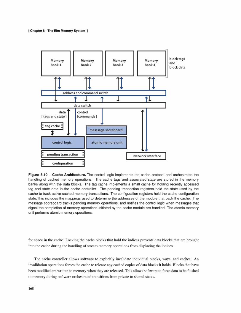
[ Chapter 8 – The Elm Memory System ]
MemoryBank 2
control logic
pending transaction
data switch
address and command switch
control [commands ]
data [ tags and state ]
messsage scoreboard
MemoryBank 4
Network Interface
MemoryBank 3
MemoryBank 1
block tagsand block data
con!guration
tag cache
atomic memory unit
Figure 8.10 – Cache Architecture. The control logic implements the cache protocol and orchestrates thehandling of cached memory operations. The cache tags and associated state are stored in the memorybanks along with the data blocks. The tag cache implements a small cache for holding recently accessedtag and state data in the cache controller. The pending transaction registers hold the state used by thecache to track active cached memory transactions. The configuration registers hold the cache configurationstate; this includes the mappings used to determine the addresses of the module that back the cache. Themessage scoreboard tracks pending memory operations, and notifies the control logic when messages thatsignal the completion of memory operations initiated by the cache module are handled. The atomic memoryunit performs atomic memory operations.
for space in the cache. Locking the cache blocks that hold the indices prevents data blocks that are broughtinto the cache during the handling of stream memory operations from displacing the indices.
The cache controller allows software to explicitly invalidate individual blocks, ways, and caches. Aninvalidation operations forces the cache to release any cached copies of data blocks it holds. Blocks that havebeen modified are written to memory when they are released. This allows software to force data to be flushedto memory during software orchestrated transitions from private to shared states.
168
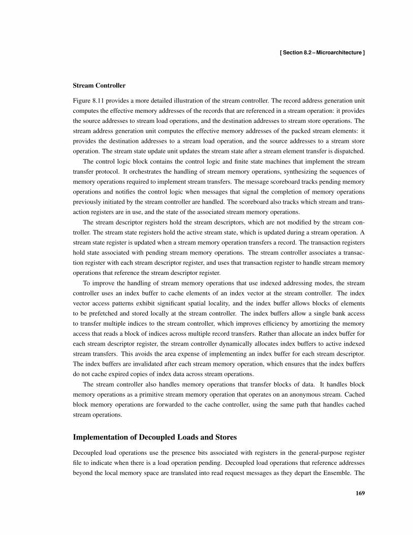
[ Section 8.2 – Microarchitecture ]
Stream Controller
Figure 8.11 provides a more detailed illustration of the stream controller. The record address generation unitcomputes the effective memory addresses of the records that are referenced in a stream operation: it providesthe source addresses to stream load operations, and the destination addresses to stream store operations. Thestream address generation unit computes the effective memory addresses of the packed stream elements: itprovides the destination addresses to a stream load operation, and the source addresses to a stream storeoperation. The stream state update unit updates the stream state after a stream element transfer is dispatched.
The control logic block contains the control logic and finite state machines that implement the streamtransfer protocol. It orchestrates the handling of stream memory operations, synthesizing the sequences ofmemory operations required to implement stream transfers. The message scoreboard tracks pending memoryoperations and notifies the control logic when messages that signal the completion of memory operationspreviously initiated by the stream controller are handled. The scoreboard also tracks which stream and trans-action registers are in use, and the state of the associated stream memory operations.
The stream descriptor registers hold the stream descriptors, which are not modified by the stream con-troller. The stream state registers hold the active stream state, which is updated during a stream operation. Astream state register is updated when a stream memory operation transfers a record. The transaction registershold state associated with pending stream memory operations. The stream controller associates a transac-tion register with each stream descriptor register, and uses that transaction register to handle stream memoryoperations that reference the stream descriptor register.
To improve the handling of stream memory operations that use indexed addressing modes, the streamcontroller uses an index buffer to cache elements of an index vector at the stream controller. The indexvector access patterns exhibit significant spatial locality, and the index buffer allows blocks of elementsto be prefetched and stored locally at the stream controller. The index buffers allow a single bank accessto transfer multiple indices to the stream controller, which improves efficiency by amortizing the memoryaccess that reads a block of indices across multiple record transfers. Rather than allocate an index buffer foreach stream descriptor register, the stream controller dynamically allocates index buffers to active indexedstream transfers. This avoids the area expense of implementing an index buffer for each stream descriptor.The index buffers are invalidated after each stream memory operation, which ensures that the index buffersdo not cache expired copies of index data across stream operations.
The stream controller also handles memory operations that transfer blocks of data. It handles blockmemory operations as a primitive stream memory operation that operates on an anonymous stream. Cachedblock memory operations are forwarded to the cache controller, using the same path that handles cachedstream operations.
Implementation of Decoupled Loads and Stores
Decoupled load operations use the presence bits associated with registers in the general-purpose registerfile to indicate when there is a load operation pending. Decoupled load operations that reference addressesbeyond the local memory space are translated into read request messages as they depart the Ensemble. The
169

[ Chapter 8 – The Elm Memory System ]
stream descriptors
stream state
record address
transaction state
stream state
stream address
control logic
message scoreboard
transaction
index bu!eractivestream state
Figure 8.11 – Stream Architecture. The transaction registers hold state associated with pending streammemory operations. The stream controller associates a transaction register with each stream descriptor regis-ter, and uses that transaction register to handle stream memory operations that reference the stream descriptorregister. The stream descriptor registers hold the stream descriptors, which are not modified by the streamcontroller. The stream state registers hold the active stream state, which is updated during a stream opera-tion. The index buffer allows the stream controller to prefetch indices when handling indexed stream memoryoperations. The index vector access patterns exhibit significant spatial locality, and the index cache allowsblocks of elements to be prefetched and stored locally at the stream controller. The message scoreboardtracks pending memory operations and notifies the control logic when messages that signal the completion ofmemory operations initiated by the stream controller are handled. The scoreboard also tracks which streamand transaction registers are in use, and the state of the associated stream memory operations.
register identifier is embedded in the source field of the message, which is used to route the returned loaddata. The memory controller that responds to the read request inserts the source address from the requestaddress into the destination field of the response message. The local memory controller extracts the registeridentifier and forwards the load value and register identifier to the processor that issued the request. Thisconvention uses the additional addresses that are available in the Ensemble address ranges to avoid having toallocate storage to record the return register addresses within the Ensemble memory controllers.
Hardware Memory Operations and Messages
This section provides a brief description how memory operations are handled. Elm allows most messageclasses to encode the number of data words contained in the payload section. This complicates the design
170
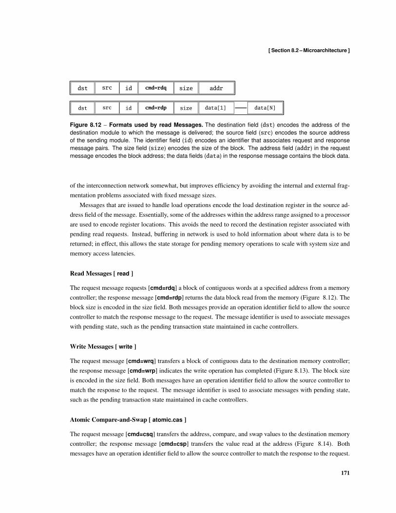
[ Section 8.2 – Microarchitecture ]
dst src id cmd=rdq size addr
dst src id cmd=rdp size data[1] data[N]
Figure 8.12 – Formats used by read Messages. The destination field (dst) encodes the address of thedestination module to which the message is delivered; the source field (src) encodes the source addressof the sending module. The identifier field (id) encodes an identifier that associates request and responsemessage pairs. The size field (size) encodes the size of the block. The address field (addr) in the requestmessage encodes the block address; the data fields (data) in the response message contains the block data.
of the interconnection network somewhat, but improves efficiency by avoiding the internal and external frag-mentation problems associated with fixed message sizes.
Messages that are issued to handle load operations encode the load destination register in the source ad-dress field of the message. Essentially, some of the addresses within the address range assigned to a processorare used to encode register locations. This avoids the need to record the destination register associated withpending read requests. Instead, buffering in network is used to hold information about where data is to bereturned; in effect, this allows the state storage for pending memory operations to scale with system size andmemory access latencies.
Read Messages [ read ]
The request message requests [cmd=rdq] a block of contiguous words at a specified address from a memorycontroller; the response message [cmd=rdp] returns the data block read from the memory (Figure 8.12). Theblock size is encoded in the size field. Both messages provide an operation identifier field to allow the sourcecontroller to match the response message to the request. The message identifier is used to associate messageswith pending state, such as the pending transaction state maintained in cache controllers.
Write Messages [ write ]
The request message [cmd=wrq] transfers a block of contiguous data to the destination memory controller;the response message [cmd=wrp] indicates the write operation has completed (Figure 8.13). The block sizeis encoded in the size field. Both messages have an operation identifier field to allow the source controller tomatch the response to the request. The message identifier is used to associate messages with pending state,such as the pending transaction state maintained in cache controllers.
Atomic Compare-and-Swap [ atomic.cas ]
The request message [cmd=csq] transfers the address, compare, and swap values to the destination memorycontroller; the response message [cmd=csp] transfers the value read at the address (Figure 8.14). Bothmessages have an operation identifier field to allow the source controller to match the response to the request.
171
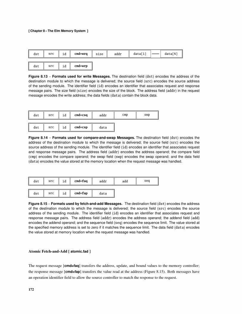
[ Chapter 8 – The Elm Memory System ]
dst src id cmd=wrq size addr data[1] data[N]
dst src id cmd=wrp
Figure 8.13 – Formats used for write Messages. The destination field (dst) encodes the address of thedestination module to which the message is delivered; the source field (src) encodes the source addressof the sending module. The identifier field (id) encodes an identifier that associates request and responsemessage pairs. The size field (size) encodes the size of the block. The address field (addr) in the requestmessage encodes the write address; the data fields (data) contain the block data.
dst src id cmd=csq addr cmp swp
dst src id cmd=csp data
Figure 8.14 – Formats used for compare-and-swap Messages. The destination field (dst) encodes theaddress of the destination module to which the message is delivered; the source field (src) encodes thesource address of the sending module. The identifier field (id) encodes an identifier that associates requestand response message pairs. The address field (addr) encodes the address operand; the compare field(cmp) encodes the compare operand; the swap field (swp) encodes the swap operand; and the data field(data) encodes the value stored at the memory location when the request message was handled.
dst src id cmd=faq addr add seq
dst src id cmd=fap data
Figure 8.15 – Formats used by fetch-and-add Messages. The destination field (dst) encodes the addressof the destination module to which the message is delivered; the source field (src) encodes the sourceaddress of the sending module. The identifier field (id) encodes an identifier that associates request andresponse message pairs. The address field (addr) encodes the address operand; the addend field (add)encodes the addend operand; and the sequence field (seq) encodes the sequence limit. The value stored atthe specified memory address is set to zero if it matches the sequence limit. The data field (data) encodesthe value stored at memory location when the request message was handled.
Atomic Fetch-and-Add [ atomic.fad ]
The request message [cmd=faq] transfers the address, update, and bound values to the memory controller;the response message [cmd=fap] transfers the value read at the address (Figure 8.15). Both messages havean operation identifier field to allow the source controller to match the response to the request.
172
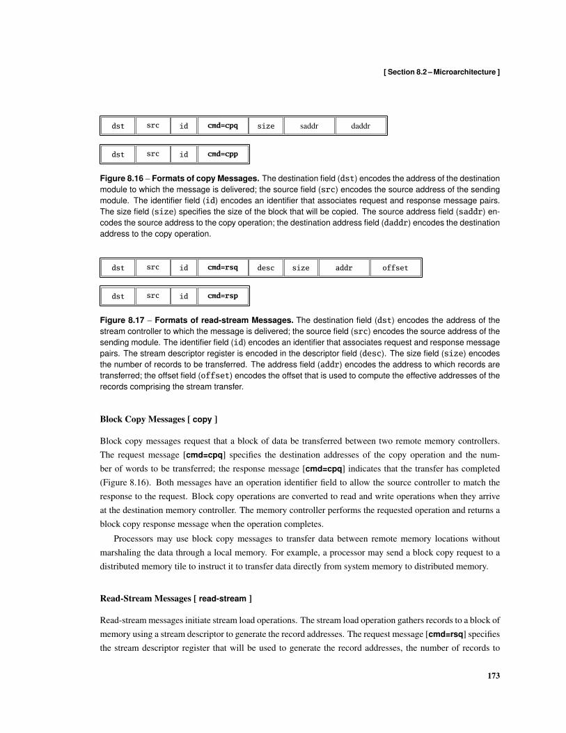
[ Section 8.2 – Microarchitecture ]
dst src id cmd=cpq size saddr daddr
dst src id cmd=cpp
Figure 8.16 – Formats of copy Messages. The destination field (dst) encodes the address of the destinationmodule to which the message is delivered; the source field (src) encodes the source address of the sendingmodule. The identifier field (id) encodes an identifier that associates request and response message pairs.The size field (size) specifies the size of the block that will be copied. The source address field (saddr) en-codes the source address to the copy operation; the destination address field (daddr) encodes the destinationaddress to the copy operation.
dst src id cmd=rsq desc size addr offset
dst src id cmd=rsp
Figure 8.17 – Formats of read-stream Messages. The destination field (dst) encodes the address of thestream controller to which the message is delivered; the source field (src) encodes the source address of thesending module. The identifier field (id) encodes an identifier that associates request and response messagepairs. The stream descriptor register is encoded in the descriptor field (desc). The size field (size) encodesthe number of records to be transferred. The address field (addr) encodes the address to which records aretransferred; the offset field (offset) encodes the offset that is used to compute the effective addresses of therecords comprising the stream transfer.
Block Copy Messages [ copy ]
Block copy messages request that a block of data be transferred between two remote memory controllers.The request message [cmd=cpq] specifies the destination addresses of the copy operation and the num-ber of words to be transferred; the response message [cmd=cpq] indicates that the transfer has completed(Figure 8.16). Both messages have an operation identifier field to allow the source controller to match theresponse to the request. Block copy operations are converted to read and write operations when they arriveat the destination memory controller. The memory controller performs the requested operation and returns ablock copy response message when the operation completes.
Processors may use block copy messages to transfer data between remote memory locations withoutmarshaling the data through a local memory. For example, a processor may send a block copy request to adistributed memory tile to instruct it to transfer data directly from system memory to distributed memory.
Read-Stream Messages [ read-stream ]
Read-stream messages initiate stream load operations. The stream load operation gathers records to a block ofmemory using a stream descriptor to generate the record addresses. The request message [cmd=rsq] specifiesthe stream descriptor register that will be used to generate the record addresses, the number of records to
173

[ Chapter 8 – The Elm Memory System ]
dst src id cmd=wsq desc size addr offset
dst src id cmd=wsp
Figure 8.18 – Formats of write-stream messages. The destination field (dst) encodes the address of thestream controller to which the message is delivered; the source field (src) encodes the source address of thesending module. The identifier field (id) encodes an identifier that associates request and response messagepairs. The stream descriptor register is encoded in the descriptor field (desc). The size field (size) encodesthe number of records to be transferred. The address field (addr) encodes the address to which records aretransferred; the offset field (offset) encodes the offset that is used to compute the effective addresses of therecords comprising the stream transfer.
dst src id cmd=rdcq size addr
dst src id cmd=rdcp size data[1] data[N]
Figure 8.19 – Formats of read-cache messages. The destination field (dst) encodes the address of thecache controller to which the message is delivered; the source field (src) encodes the source address of thesending module. The identifier field (id) encodes an identifier that associates request and response messagepairs. The size field (size) encodes the size of the block. The address field (addr) in the request messageencodes the block address; the data fields (data) in the response message contains the block data.
be transferred, and the address at which the records are to be moved. The response message [cmd=rsp]is returned when the stream controller completes the operation. The stream controller orchestrating theoperation issues sequences of read, write, and block copy messages to effect the stream transfer.
Write-Stream Messages [write-stream]
Write-stream messages initiate stream store operations. The stream store operation scatters records from ablock of memory using a stream descriptor to generate the record addresses. The request message [cmd=wsq]specifies the stream descriptor register that will be used to generate the record addresses, the number ofrecords to be transferred, and the address from which the records are to be moved. The response message[cmd=wsp] is returned when the stream controller completes the operation. The stream controller orches-trating the operation issues sequences of read, write, and block copy messages to effect the stream transfer.
Read-Cache Messages [ read-cache ]
These messages load blocks of data using a distributed memory as block cache. The request message[cmd=rdcq] transfers the block address and block size to a cache controller; the response message [cmd=rdcp]returns the data block (Figure 8.19).
174
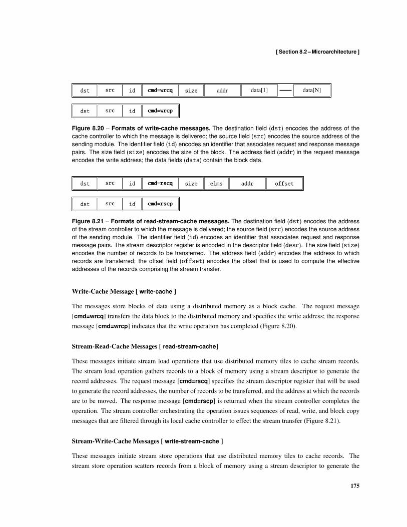
[ Section 8.2 – Microarchitecture ]
dst src id cmd=wrcq size addr data[1] data[N]
dst src id cmd=wrcp
Figure 8.20 – Formats of write-cache messages. The destination field (dst) encodes the address of thecache controller to which the message is delivered; the source field (src) encodes the source address of thesending module. The identifier field (id) encodes an identifier that associates request and response messagepairs. The size field (size) encodes the size of the block. The address field (addr) in the request messageencodes the write address; the data fields (data) contain the block data.
dst src id cmd=rscq size elms addr offset
dst src id cmd=rscp
Figure 8.21 – Formats of read-stream-cache messages. The destination field (dst) encodes the addressof the stream controller to which the message is delivered; the source field (src) encodes the source addressof the sending module. The identifier field (id) encodes an identifier that associates request and responsemessage pairs. The stream descriptor register is encoded in the descriptor field (desc). The size field (size)encodes the number of records to be transferred. The address field (addr) encodes the address to whichrecords are transferred; the offset field (offset) encodes the offset that is used to compute the effectiveaddresses of the records comprising the stream transfer.
Write-Cache Message [ write-cache ]
The messages store blocks of data using a distributed memory as a block cache. The request message[cmd=wrcq] transfers the data block to the distributed memory and specifies the write address; the responsemessage [cmd=wrcp] indicates that the write operation has completed (Figure 8.20).
Stream-Read-Cache Messages [ read-stream-cache]
These messages initiate stream load operations that use distributed memory tiles to cache stream records.The stream load operation gathers records to a block of memory using a stream descriptor to generate therecord addresses. The request message [cmd=rscq] specifies the stream descriptor register that will be usedto generate the record addresses, the number of records to be transferred, and the address at which the recordsare to be moved. The response message [cmd=rscp] is returned when the stream controller completes theoperation. The stream controller orchestrating the operation issues sequences of read, write, and block copymessages that are filtered through its local cache controller to effect the stream transfer (Figure 8.21).
Stream-Write-Cache Messages [ write-stream-cache ]
These messages initiate stream store operations that use distributed memory tiles to cache records. Thestream store operation scatters records from a block of memory using a stream descriptor to generate the
175
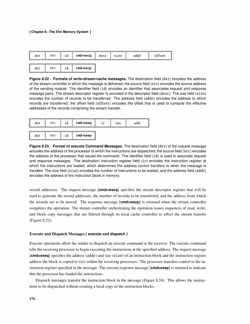
[ Chapter 8 – The Elm Memory System ]
dst src id cmd=wscq desc size addr offset
dst src id cmd=wscp
Figure 8.22 – Formats of write-stream-cache messages. The destination field (dst) encodes the addressof the stream controller to which the message is delivered; the source field (src) encodes the source addressof the sending module. The identifier field (id) encodes an identifier that associates request and responsemessage pairs. The stream descriptor register is encoded in the descriptor field (desc). The size field (size)encodes the number of records to be transferred. The address field (addr) encodes the address to whichrecords are transferred; the offset field (offset) encodes the offset that is used to compute the effectiveaddresses of the records comprising the stream transfer.
dst src id cmd=exeq ir size addr
dst src id cmd=exep
Figure 8.23 – Format of execute Command Messages. The destination field (dst) of the request messageencodes the address of the processor to which the instructions are dispatched; the source field (src) encodesthe address of the processor that issued the command. The identifier field (id) is used to associate requestand response messages. The destination instruction register field (ir) encodes the instruction register atwhich the instructions are loaded, which determines the address control transfers to when the message ishandled. The size field (size) encodes the number of instructions to be loaded, and the address field (addr)encodes the address of the instruction block in memory.
record addresses. The request message [cmd=wscq] specifies the stream descriptor register that will beused to generate the record addresses, the number of records to be transferred, and the address from whichthe records are to be moved. The response message [cmd=wscp] is returned when the stream controllercompletes the operation. The stream controller orchestrating the operation issues sequences of read, write,and block copy messages that are filtered through its local cache controller to effect the stream transfer(Figure 8.22).
Execute and Dispatch Messages [ execute and dispatch ]
Execute operations allow the sender to dispatch an execute command at the receiver. The execute commandtells the receiving processor to begin executing the instructions at the specified address. The request message[cmd=exeq] specifies the address (addr) and size (size) of an instruction block and the instruction registeraddress the block is copied to (ir) within the receiving processors. The processor transfers control to the in-struction register specified in the message. The execute response message [cmd=exep] is returned to indicatethat the processor has loaded the instructions.
Dispatch messages transfer the instruction block in the message (Figure 8.24). This allows the instruc-tions to be dispatched without creating a local copy of the instruction blocks.
176
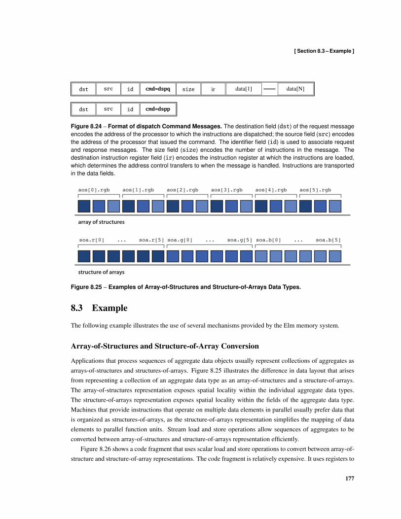
[ Section 8.3 – Example ]
dst src id cmd=dspq size ir data[1] data[N]
dst src id cmd=dspp
Figure 8.24 – Format of dispatch Command Messages. The destination field (dst) of the request messageencodes the address of the processor to which the instructions are dispatched; the source field (src) encodesthe address of the processor that issued the command. The identifier field (id) is used to associate requestand response messages. The size field (size) encodes the number of instructions in the message. Thedestination instruction register field (ir) encodes the instruction register at which the instructions are loaded,which determines the address control transfers to when the message is handled. Instructions are transportedin the data fields.
aos[0].rgb aos[1].rgb
soa.r[0] ... soa.r[5]
aos[2].rgb aos[3].rgb aos[4].rgb aos[5].rgb
structure of arrays
array of structures
soa.g[0] ... soa.g[5] soa.b[0] ... soa.b[5]
Figure 8.25 – Examples of Array-of-Structures and Structure-of-Arrays Data Types.
8.3 Example
The following example illustrates the use of several mechanisms provided by the Elm memory system.
Array-of-Structures and Structure-of-Array Conversion
Applications that process sequences of aggregate data objects usually represent collections of aggregates asarrays-of-structures and structures-of-arrays. Figure 8.25 illustrates the difference in data layout that arisesfrom representing a collection of an aggregate data type as an array-of-structures and a structure-of-arrays.The array-of-structures representation exposes spatial locality within the individual aggregate data types.The structure-of-arrays representation exposes spatial locality within the fields of the aggregate data type.Machines that provide instructions that operate on multiple data elements in parallel usually prefer data thatis organized as structures-of-arrays, as the structure-of-arrays representation simplifies the mapping of dataelements to parallel function units. Stream load and store operations allow sequences of aggregates to beconverted between array-of-structures and structure-of-arrays representation efficiently.
Figure 8.26 shows a code fragment that uses scalar load and store operations to convert between array-of-structure and structure-of-array representations. The code fragment is relatively expensive. It uses registers to
177

[ Chapter 8 – The Elm Memory System ]
for ( int j = 0; j < 6; j++ ) { soa.r[j] = aos[j].r; soa.g[j] = aos[j].g; soa.b[j] = aos[j].b;}
// array-of-structures to structure-of-arrays
for ( int j = 0; j < 6; j++ ) { aos[j].r = soa.r[j]; aos[j].g = soa.g[j]; aos[j].b = soa.b[j];}
// structure-of-arrays to array-of-structures
100101102103104105106107108109110111112113114115
struct { fixed32 r; fixed32 g; fixed32 b; } aos[6];struct { fixed32 r[6]; fixed32 g[6]; fixed32 b[6] } soa;
Figure 8.26 – Scalar Conversion Between Array-of-Structures and Structure-of-Arrays.
stream_descriptor sd = { 1, // stream record-size 6, // number of records in stream 1, // stream element stride 0 }; // index address (null)
struct { fixed32 r; fixed32 g; fixed32 b; } aos[6];struct { fixed32 r[6]; fixed32 g[6]; fixed32 b[6] } soa;
stream_load( &soa.r, &aos.r, &sd );// array-of-structures to structure-of-arrays
// structure-of-arrays to array-of-structures
100101102103104105106107108109110111112113114115
stream_load( &soa.g, &aos.g, &sd );stream_load( &soa.b, &aos.b, &sd );
stream_store( &aos.r, &soa.r, &sd );stream_store( &aos.g, &soa.g, &sd );stream_store( &aos.b, &soa.b, &sd );
stream_sync();
stream_sync();116117
Figure 8.27 – Stream Conversion Between Array-of-Structures and Structures-of-Arrays.
stage data and function units to orchestrate the movement of individual elements. The number of instructionsthat are executed increases in proportion to the number of data elements that are moved, which is the productof the array length and the number of elements in the aggregate data type.
Figure 8.27 shows an equivalent code fragment that uses stream load and store operations to convertbetween array-of-structure and structure-of-array representations. Data is moved between memory locationswithout passing through registers. The function units are used to initiate and coordinate the synchronizationof the data movement, but are not used to orchestrate the movement of individual elements. The number ofinstructions that are executed increases in proportion to the number of elements in the aggregate data type,and is independent of the array length.
178
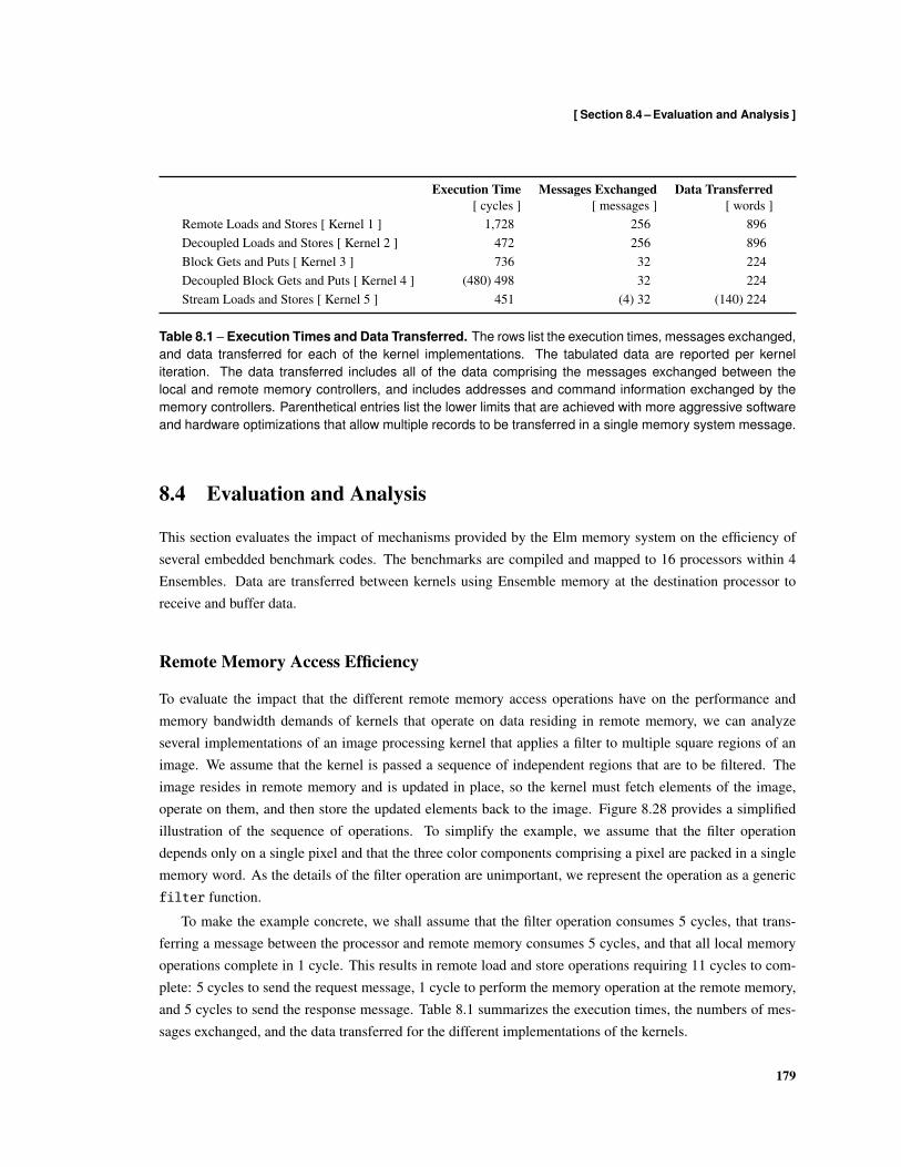
[ Section 8.4 – Evaluation and Analysis ]
Execution Time Messages Exchanged Data Transferred[ cycles ] [ messages ] [ words ]
Remote Loads and Stores [ Kernel 1 ] 1,728 256 896Decoupled Loads and Stores [ Kernel 2 ] 472 256 896Block Gets and Puts [ Kernel 3 ] 736 32 224Decoupled Block Gets and Puts [ Kernel 4 ] (480) 498 32 224Stream Loads and Stores [ Kernel 5 ] 451 (4) 32 (140) 224
Table 8.1 – Execution Times and Data Transferred. The rows list the execution times, messages exchanged,and data transferred for each of the kernel implementations. The tabulated data are reported per kerneliteration. The data transferred includes all of the data comprising the messages exchanged between thelocal and remote memory controllers, and includes addresses and command information exchanged by thememory controllers. Parenthetical entries list the lower limits that are achieved with more aggressive softwareand hardware optimizations that allow multiple records to be transferred in a single memory system message.
8.4 Evaluation and Analysis
This section evaluates the impact of mechanisms provided by the Elm memory system on the efficiency ofseveral embedded benchmark codes. The benchmarks are compiled and mapped to 16 processors within 4Ensembles. Data are transferred between kernels using Ensemble memory at the destination processor toreceive and buffer data.
Remote Memory Access Efficiency
To evaluate the impact that the different remote memory access operations have on the performance andmemory bandwidth demands of kernels that operate on data residing in remote memory, we can analyzeseveral implementations of an image processing kernel that applies a filter to multiple square regions of animage. We assume that the kernel is passed a sequence of independent regions that are to be filtered. Theimage resides in remote memory and is updated in place, so the kernel must fetch elements of the image,operate on them, and then store the updated elements back to the image. Figure 8.28 provides a simplifiedillustration of the sequence of operations. To simplify the example, we assume that the filter operationdepends only on a single pixel and that the three color components comprising a pixel are packed in a singlememory word. As the details of the filter operation are unimportant, we represent the operation as a genericfilter function.
To make the example concrete, we shall assume that the filter operation consumes 5 cycles, that trans-ferring a message between the processor and remote memory consumes 5 cycles, and that all local memoryoperations complete in 1 cycle. This results in remote load and store operations requiring 11 cycles to com-plete: 5 cycles to send the request message, 1 cycle to perform the memory operation at the remote memory,and 5 cycles to send the response message. Table 8.1 summarizes the execution times, the numbers of mes-sages exchanged, and the data transferred for the different implementations of the kernels.
179
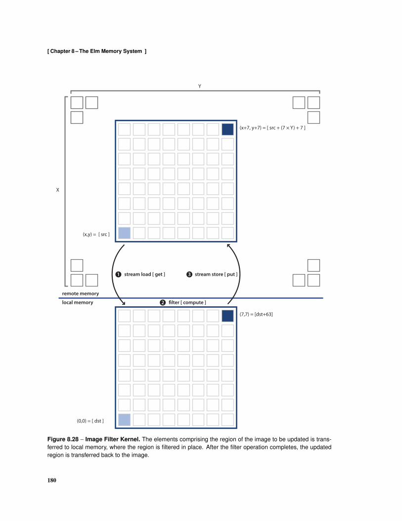
[ Chapter 8 – The Elm Memory System ]
(0,0) = [ dst ]
(7,7) = [dst+63]
(x,y) = [ src ]
(x+7, y+7) = [ src + (7 ! Y) + 7 ]
Y
X
remote memory
local memory
stream store [ put ]1
2
3
!lter [ compute ]
stream load [ get ]
Figure 8.28 – Image Filter Kernel. The elements comprising the region of the image to be updated is trans-ferred to local memory, where the region is filtered in place. After the filter operation completes, the updatedregion is transferred back to the image.
180
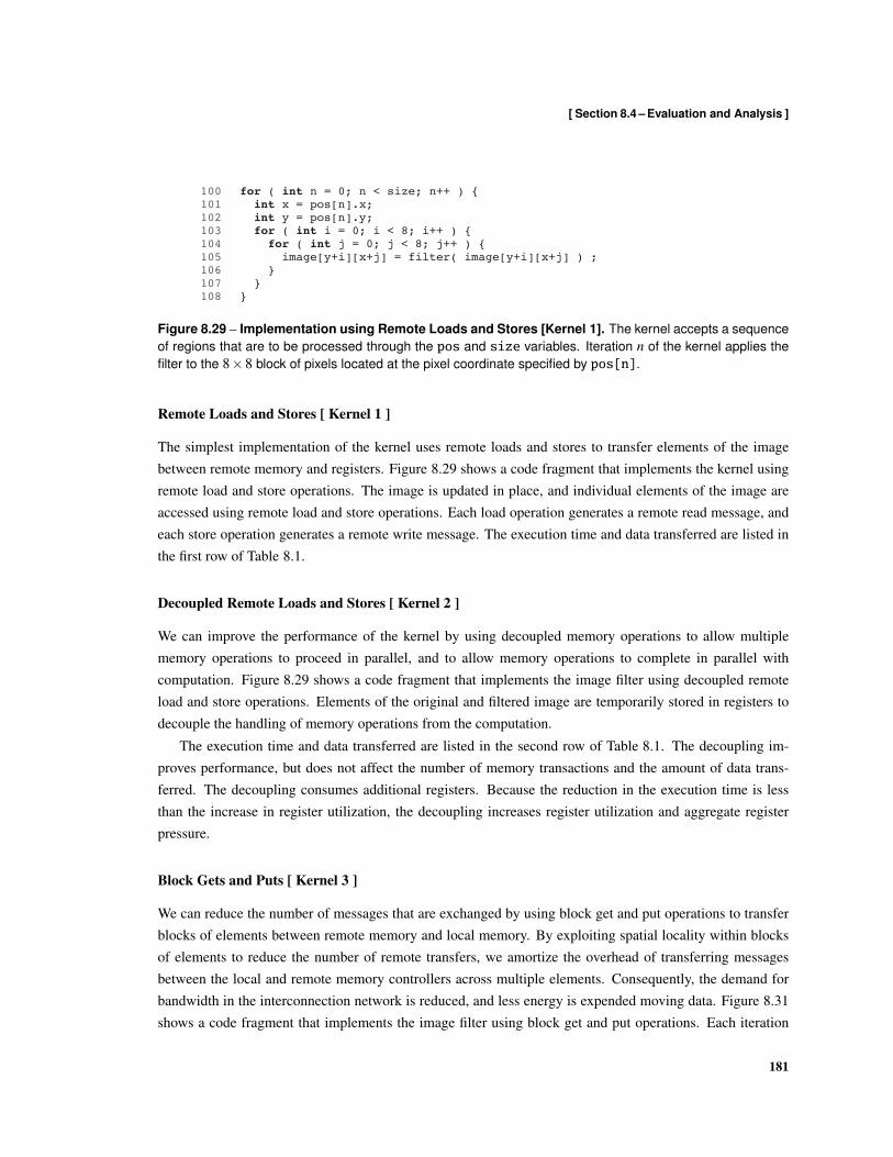
[ Section 8.4 – Evaluation and Analysis ]
for ( int j = 0; j < 8; j++ ) { for ( int i = 0; i < 8; i++ ) {
} }
image[y+i][x+j] = filter( image[y+i][x+j] ) ;
for ( int n = 0; n < size; n++ ) { int x = pos[n].x; int y = pos[n].y;
}
100101102103104105106107108
Figure 8.29 – Implementation using Remote Loads and Stores [Kernel 1]. The kernel accepts a sequenceof regions that are to be processed through the pos and size variables. Iteration n of the kernel applies thefilter to the 8×8 block of pixels located at the pixel coordinate specified by pos[n].
Remote Loads and Stores [ Kernel 1 ]
The simplest implementation of the kernel uses remote loads and stores to transfer elements of the imagebetween remote memory and registers. Figure 8.29 shows a code fragment that implements the kernel usingremote load and store operations. The image is updated in place, and individual elements of the image areaccessed using remote load and store operations. Each load operation generates a remote read message, andeach store operation generates a remote write message. The execution time and data transferred are listed inthe first row of Table 8.1.
Decoupled Remote Loads and Stores [ Kernel 2 ]
We can improve the performance of the kernel by using decoupled memory operations to allow multiplememory operations to proceed in parallel, and to allow memory operations to complete in parallel withcomputation. Figure 8.29 shows a code fragment that implements the image filter using decoupled remoteload and store operations. Elements of the original and filtered image are temporarily stored in registers todecouple the handling of memory operations from the computation.
The execution time and data transferred are listed in the second row of Table 8.1. The decoupling im-proves performance, but does not affect the number of memory transactions and the amount of data trans-ferred. The decoupling consumes additional registers. Because the reduction in the execution time is lessthan the increase in register utilization, the decoupling increases register utilization and aggregate registerpressure.
Block Gets and Puts [ Kernel 3 ]
We can reduce the number of messages that are exchanged by using block get and put operations to transferblocks of elements between remote memory and local memory. By exploiting spatial locality within blocksof elements to reduce the number of remote transfers, we amortize the overhead of transferring messagesbetween the local and remote memory controllers across multiple elements. Consequently, the demand forbandwidth in the interconnection network is reduced, and less energy is expended moving data. Figure 8.31shows a code fragment that implements the image filter using block get and put operations. Each iteration
181

[ Chapter 8 – The Elm Memory System ]
for ( int j = 0; j < 8; j++ ) { for ( int i = 0; i < 8; i++ ) {
}
image[y+i][x+j] = to[j];
ti[j] = image[y+i][x+j];
to[j] = filter( ti[j] ); for ( int j = 0; j < 8; j++ ) {
for ( int j = 0; j < 8; j++ ) {
for ( int n = 0; n < size; n++ ) { int x = pos[n].x; int y = pos[n].y;
}
fixed32 ti[8], to[8];
}
}
}
100101102103104105106107108109110111112113114115
Figure 8.30 – Implementation using Decoupled Remote Loads and Stores [Kernel 2]. Temporary vari-ables ti and to provide local storage for staging transfers from and to remote memory. The temporaryvariables are mapped to registers, and the remote memory accesses are implemented as decoupled remoteload and store operations.
for ( int i = 0; i < 8; i++ ) {
} block_put( &to, &image[y+i][x], 8);
fixed32 ti[8], to[8];
to[j] = filter( ti[j] ); for ( int j = 0; j < 8; j++ ) { block_get( &ti, &image[y+i][x], 8);
for ( int n = 0; n < size; n++ ) { int x = pos[n].x; int y = pos[n].y;
}
}
100101102103104105106107108109110111
Figure 8.31 – Implementation using Block Gets and Puts [Kernel 3]. Temporary variables ti and to pro-vide local storage for staging transfers from and to remote memory. Local memory is used to stage remotememory accesses, and the temporary variables are mapped to local memory. Data are transferred betweenlocal and remote memory using get and put operations; data are transferred between local memory and reg-isters using load and store operations.
transfers one row of the update region to local memory, performs the filter operation locally, and then transfersthe filtered row back to the image.
The execution time and data transferred are listed in the third row of Table 8.1. The block gets and putsexploit spatial locality within the rows of the update region. Using block gets and puts to transfer data betweenremote memory and local memory reduces the number of remote memory transactions and messages. Thereduction in the number of memory transactions achieves an execution time that is less than the version of thecode that uses remote loads and stores. However, the failure to overlap memory accesses and computationresults in an execution time that is greater than the version that uses decoupled loads and stores.
182
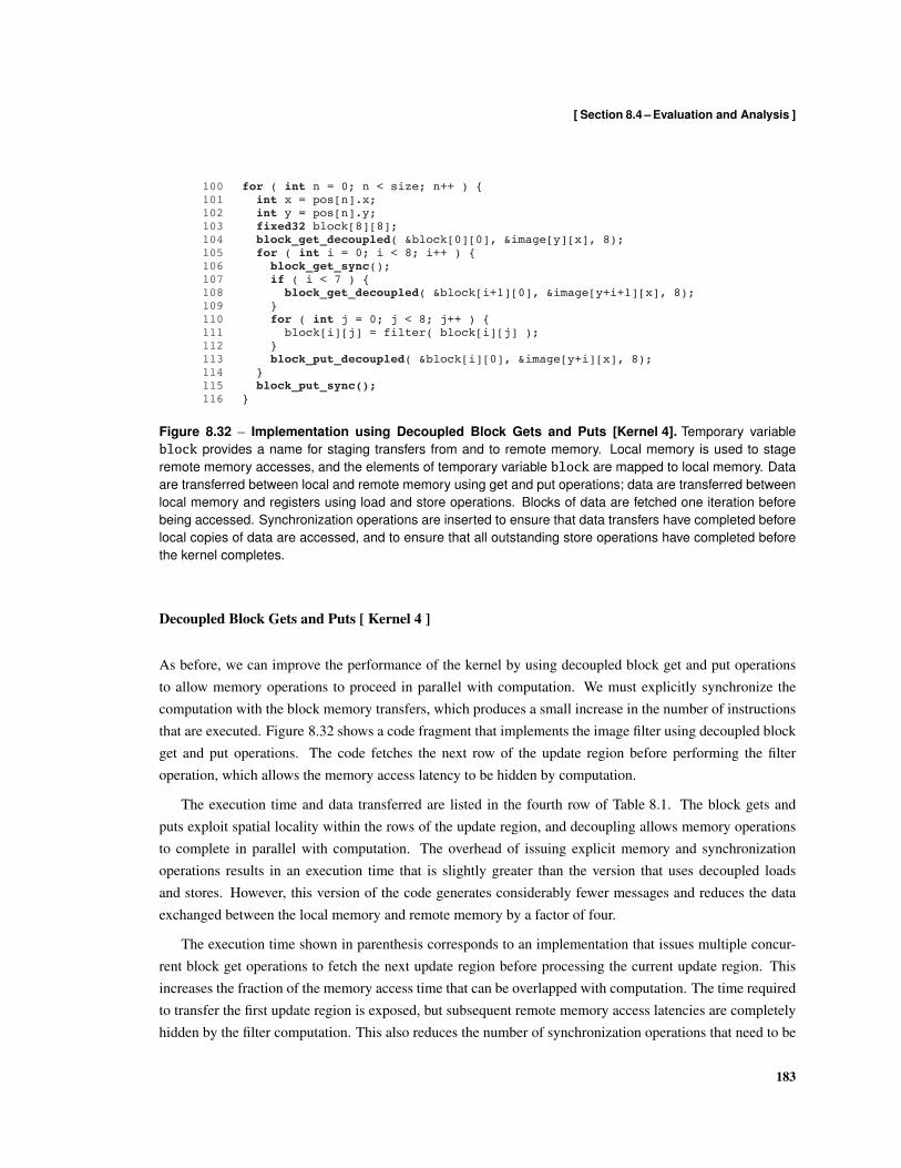
[ Section 8.4 – Evaluation and Analysis ]
for ( int i = 0; i < 8; i++ ) {
} block_put_decoupled( &block[i][0], &image[y+i][x], 8);
block[i][j] = filter( block[i][j] ); for ( int j = 0; j < 8; j++ ) {
if ( i < 7 ) {
fixed32 block[8][8]; block_get_decoupled( &block[0][0], &image[y][x], 8);
block_get_sync();
block_get_decoupled( &block[i+1][0], &image[y+i+1][x], 8);
block_put_sync();
for ( int n = 0; n < size; n++ ) { int x = pos[n].x; int y = pos[n].y;
}
}
}
100101102103104105106107108109110111112113114115116
Figure 8.32 – Implementation using Decoupled Block Gets and Puts [Kernel 4]. Temporary variableblock provides a name for staging transfers from and to remote memory. Local memory is used to stageremote memory accesses, and the elements of temporary variable block are mapped to local memory. Dataare transferred between local and remote memory using get and put operations; data are transferred betweenlocal memory and registers using load and store operations. Blocks of data are fetched one iteration beforebeing accessed. Synchronization operations are inserted to ensure that data transfers have completed beforelocal copies of data are accessed, and to ensure that all outstanding store operations have completed beforethe kernel completes.
Decoupled Block Gets and Puts [ Kernel 4 ]
As before, we can improve the performance of the kernel by using decoupled block get and put operationsto allow memory operations to proceed in parallel with computation. We must explicitly synchronize thecomputation with the block memory transfers, which produces a small increase in the number of instructionsthat are executed. Figure 8.32 shows a code fragment that implements the image filter using decoupled blockget and put operations. The code fetches the next row of the update region before performing the filteroperation, which allows the memory access latency to be hidden by computation.
The execution time and data transferred are listed in the fourth row of Table 8.1. The block gets andputs exploit spatial locality within the rows of the update region, and decoupling allows memory operationsto complete in parallel with computation. The overhead of issuing explicit memory and synchronizationoperations results in an execution time that is slightly greater than the version that uses decoupled loadsand stores. However, this version of the code generates considerably fewer messages and reduces the dataexchanged between the local memory and remote memory by a factor of four.
The execution time shown in parenthesis corresponds to an implementation that issues multiple concur-rent block get operations to fetch the next update region before processing the current update region. Thisincreases the fraction of the memory access time that can be overlapped with computation. The time requiredto transfer the first update region is exposed, but subsequent remote memory access latencies are completelyhidden by the filter computation. This also reduces the number of synchronization operations that need to be
183
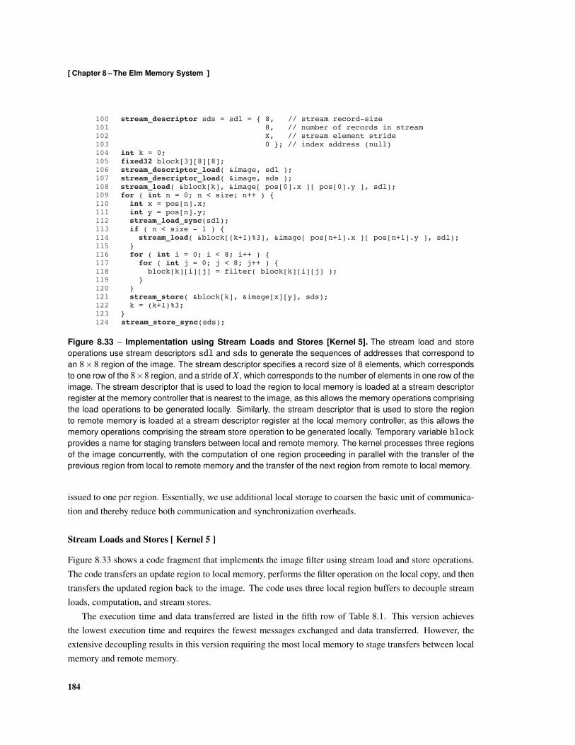
[ Chapter 8 – The Elm Memory System ]
for ( int n = 0; n < size; n++ ) { int x = pos[n].x; int y = pos[n].y;
fixed32 block[3][8][8];int k = 0;
stream_load( &block[k], &image[ pos[0].x ][ pos[0].y ], sdl);
if ( n < size - 1 ) { stream_load( &block[(k+1)%3], &image[ pos[n+1].x ][ pos[n+1].y ], sdl);
stream_load_sync(sdl);
for ( int j = 0; j < 8; j++ ) { for ( int i = 0; i < 8; i++ ) {
block[k][i][j] = filter( block[k][i][j] ); } }
}
stream_store( &block[k], &image[x][y], sds); k = (k+1)%3;}
100101102103104105106107108109110111112113114115116117
stream_descriptor sds = sdl = { 8, // stream record-size 8, // number of records in stream X, // stream element stride 0 }; // index address (null)
118119120121
stream_descriptor_load( &image, sdl );
122123124
stream_descriptor_load( &image, sds );
stream_store_sync(sds);
Figure 8.33 – Implementation using Stream Loads and Stores [Kernel 5]. The stream load and storeoperations use stream descriptors sdl and sds to generate the sequences of addresses that correspond toan 8×8 region of the image. The stream descriptor specifies a record size of 8 elements, which correspondsto one row of the 8×8 region, and a stride of X , which corresponds to the number of elements in one row of theimage. The stream descriptor that is used to load the region to local memory is loaded at a stream descriptorregister at the memory controller that is nearest to the image, as this allows the memory operations comprisingthe load operations to be generated locally. Similarly, the stream descriptor that is used to store the regionto remote memory is loaded at a stream descriptor register at the local memory controller, as this allows thememory operations comprising the stream store operation to be generated locally. Temporary variable blockprovides a name for staging transfers between local and remote memory. The kernel processes three regionsof the image concurrently, with the computation of one region proceeding in parallel with the transfer of theprevious region from local to remote memory and the transfer of the next region from remote to local memory.
issued to one per region. Essentially, we use additional local storage to coarsen the basic unit of communica-tion and thereby reduce both communication and synchronization overheads.
Stream Loads and Stores [ Kernel 5 ]
Figure 8.33 shows a code fragment that implements the image filter using stream load and store operations.The code transfers an update region to local memory, performs the filter operation on the local copy, and thentransfers the updated region back to the image. The code uses three local region buffers to decouple streamloads, computation, and stream stores.
The execution time and data transferred are listed in the fifth row of Table 8.1. This version achievesthe lowest execution time and requires the fewest messages exchanged and data transferred. However, theextensive decoupling results in this version requiring the most local memory to stage transfers between localmemory and remote memory.
184
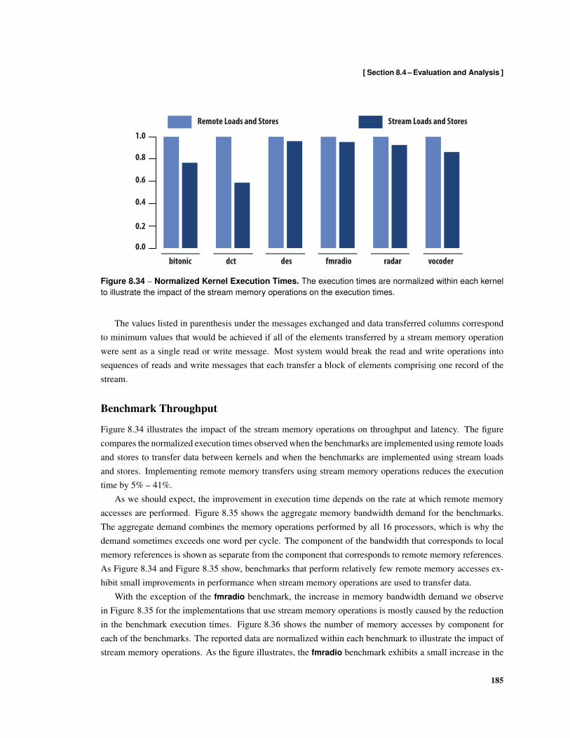
[ Section 8.4 – Evaluation and Analysis ]
0.0
0.2
0.4
0.6
0.8
1.0
bitonic
Remote Loads and Stores Stream Loads and Stores
dct des fmradio radar vocoder
Figure 8.34 – Normalized Kernel Execution Times. The execution times are normalized within each kernelto illustrate the impact of the stream memory operations on the execution times.
The values listed in parenthesis under the messages exchanged and data transferred columns correspondto minimum values that would be achieved if all of the elements transferred by a stream memory operationwere sent as a single read or write message. Most system would break the read and write operations intosequences of reads and write messages that each transfer a block of elements comprising one record of thestream.
Benchmark Throughput
Figure 8.34 illustrates the impact of the stream memory operations on throughput and latency. The figurecompares the normalized execution times observed when the benchmarks are implemented using remote loadsand stores to transfer data between kernels and when the benchmarks are implemented using stream loadsand stores. Implementing remote memory transfers using stream memory operations reduces the executiontime by 5% – 41%.
As we should expect, the improvement in execution time depends on the rate at which remote memoryaccesses are performed. Figure 8.35 shows the aggregate memory bandwidth demand for the benchmarks.The aggregate demand combines the memory operations performed by all 16 processors, which is why thedemand sometimes exceeds one word per cycle. The component of the bandwidth that corresponds to localmemory references is shown as separate from the component that corresponds to remote memory references.As Figure 8.34 and Figure 8.35 show, benchmarks that perform relatively few remote memory accesses ex-hibit small improvements in performance when stream memory operations are used to transfer data.
With the exception of the fmradio benchmark, the increase in memory bandwidth demand we observein Figure 8.35 for the implementations that use stream memory operations is mostly caused by the reductionin the benchmark execution times. Figure 8.36 shows the number of memory accesses by component foreach of the benchmarks. The reported data are normalized within each benchmark to illustrate the impact ofstream memory operations. As the figure illustrates, the fmradio benchmark exhibits a small increase in the
185
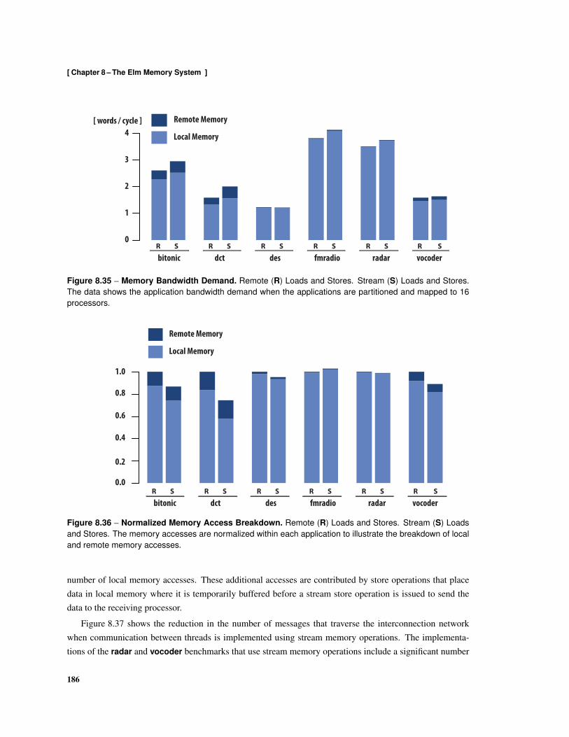
[ Chapter 8 – The Elm Memory System ]
Remote Memory
Local Memory
[ words / cycle ]
0
1
2
3
4
bitonic dct des fmradio radar vocoderR S R S R S R S R S R S
Figure 8.35 – Memory Bandwidth Demand. Remote (R) Loads and Stores. Stream (S) Loads and Stores.The data shows the application bandwidth demand when the applications are partitioned and mapped to 16processors.
0.0
0.2
0.4
0.6
0.8
1.0
Remote Memory
Local Memory
bitonic dct des fmradio radar vocoderR S R S R S R S R S R S
Figure 8.36 – Normalized Memory Access Breakdown. Remote (R) Loads and Stores. Stream (S) Loadsand Stores. The memory accesses are normalized within each application to illustrate the breakdown of localand remote memory accesses.
number of local memory accesses. These additional accesses are contributed by store operations that placedata in local memory where it is temporarily buffered before a stream store operation is issued to send thedata to the receiving processor.
Figure 8.37 shows the reduction in the number of messages that traverse the interconnection networkwhen communication between threads is implemented using stream memory operations. The implementa-tions of the radar and vocoder benchmarks that use stream memory operations include a significant number
186

[ Section 8.4 – Evaluation and Analysis ]
Remote Memory Operationsbitonic dct des fmradio radar vocoder
8,852 7,361 5,542 18,136 50,261 788,773
Stream Memory Operationsbitonic dct des fmradio radar vocoder
(16, 1) 6,673 (16, 1) 2,766 (8, 1) 260 (8, 1) 4,320 (1, 2) 25,123 (1, 1) 316,994(32, 1) 1,550 (32, 1) 1,085 (16, 1) 715 (16, 1) 3,254 (2, 2) 1,049 (2, 1) 92,624
(64, 1) 110 (64, 1) 120 (4, 2) 526 (8, 1) 3,598(16, 2) 282 (32, 2) 198 (15, 1) 7,710(64, 2) 37 (64, 2) 105 (20, 1) 4,112
(96, 1) 2,569(1, 2) 63,909
Table 8.2 – Number of Remote and Stream Memory Operations in Benchmarks. The stream operationentries use the syntax (e,w) to indicate that the stream operation transfers a sequence of e elements, witheach element comprising w contiguous words.
0.0
0.2
0.4
0.6
0.8
1.0
bitonic dct des fmradio radar vocoderR S R S R S R S R S R S
Figure 8.37 – Normalized Memory Messages. (R) Remote Loads and Stores. (S) Stream Loads and Stores.The data presented in the figure are normalized to illustrate the reduction in the number of messages that arecommunicated when the applications are implemented using stream load and store operations.
of remote load and store operations that access scalar variables. Table 8.2 lists the number of remote mem-ory operations and stream memory operations performed in the implementations that use stream memoryoperations. Most of the scalar operations reference coordination variables that are used to synchronize theexecution of the kernels and to interleave the enqueuing and dequeuing of data at distributed queues; otheroperations reference scalar data that is distributed across multiple Ensembles. The scalar references accountfor the smaller reduction in the number of messages we observe for these benchmarks in Figure 8.37.
Remote load and store operations produce messages that transport a single word of application data.Most stream memory operations produce messages that transport multiple words of application data, whichamortizes the overhead of the message header over more application data. Figure 8.37 shows the the amountof data that traverses the interconnection network, which includes both application data, message header data,and acknowledgment messages sent in response when required by the message communication protocol. The
187
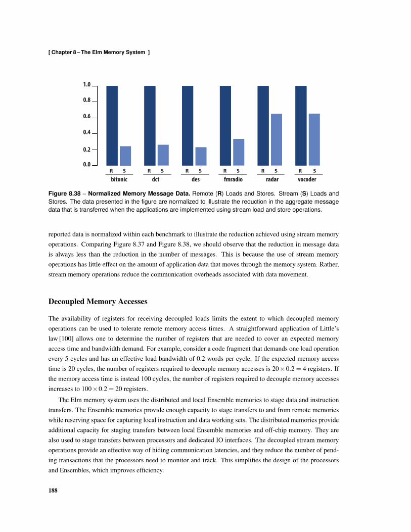
[ Chapter 8 – The Elm Memory System ]
0.0
0.2
0.4
0.6
0.8
1.0
bitonic dct des fmradio radar vocoderR S R S R S R S R S R S
Figure 8.38 – Normalized Memory Message Data. Remote (R) Loads and Stores. Stream (S) Loads andStores. The data presented in the figure are normalized to illustrate the reduction in the aggregate messagedata that is transferred when the applications are implemented using stream load and store operations.
reported data is normalized within each benchmark to illustrate the reduction achieved using stream memoryoperations. Comparing Figure 8.37 and Figure 8.38, we should observe that the reduction in message datais always less than the reduction in the number of messages. This is because the use of stream memoryoperations has little effect on the amount of application data that moves through the memory system. Rather,stream memory operations reduce the communication overheads associated with data movement.
Decoupled Memory Accesses
The availability of registers for receiving decoupled loads limits the extent to which decoupled memoryoperations can be used to tolerate remote memory access times. A straightforward application of Little’slaw [100] allows one to determine the number of registers that are needed to cover an expected memoryaccess time and bandwidth demand. For example, consider a code fragment that demands one load operationevery 5 cycles and has an effective load bandwidth of 0.2 words per cycle. If the expected memory accesstime is 20 cycles, the number of registers required to decouple memory accesses is 20×0.2 = 4 registers. Ifthe memory access time is instead 100 cycles, the number of registers required to decouple memory accessesincreases to 100×0.2 = 20 registers.
The Elm memory system uses the distributed and local Ensemble memories to stage data and instructiontransfers. The Ensemble memories provide enough capacity to stage transfers to and from remote memorieswhile reserving space for capturing local instruction and data working sets. The distributed memories provideadditional capacity for staging transfers between local Ensemble memories and off-chip memory. They arealso used to stage transfers between processors and dedicated IO interfaces. The decoupled stream memoryoperations provide an effective way of hiding communication latencies, and they reduce the number of pend-ing transactions that the processors need to monitor and track. This simplifies the design of the processorsand Ensembles, which improves efficiency.
188
[ Section 8.5 – Related Work ]
8.5 Related Work
Contemporary microprocessors rely extensively on hardware cache hierarchies to reduce apparent memoryaccess latencies [133]. Processor designs commonly use cache block sizes that are larger than the machineword size, and transfer an entire cache block on a miss to provide a limited amount of hardware prefetchingwithin the block.
Superscalar processors use out-of-order execution and non-blocking caches to hide memory access laten-cies by overlapping memory operations and with the execution of independent instructions [6, 79]. Registerrenaming is used to expose additional instruction-level parallelism, and allows processors to initiate moreconcurrent memory operations [152]. Speculative execution allows processors to calculate addresses andinitiate cache refills early [152], which helps to reduce apparent memory access times. In addition to thestructures used to track pending misses in the caches, superscalar processors use registers in the multi-portedrenamed register file to receive data returned by load operations, and structures such as the instruction win-dow and the memory reorder queue to record the state of pending memory operations. These structures arevery expensive, which limits the extent to which superscalar processors can use out-of-order execution tohide memory access latencies.
Many high-performance processors use dedicated hardware prefetch units to speculatively fetch blocksthat are expected to be accessed before the instructions that reference the blocks reach the memory sys-tem [72]. Because most attempt to predict future misses based on observed address miss patterns, hardwareprefetch units are more effective when data and instruction access patterns exhibit significant amounts ofstructure and regularity. Consequently, they typically fail to comprehend complex access patterns and mayfetch data that is never referenced before being released from the cache. Miss-based hardware prefetchschemes are typically only effective when data access patterns generate long stable address sequences be-cause they require one or more misses to detect the access pattern. Hardware prefetch schemes typicallyprefetch beyond the end of a sequence. Dedicated stream buffers may be used to avoid polluting the datacache when the prefetched data is not accessed [72], though the misprediction wastes energy and memorysystem bandwidth.
Most miss-based hardware prefetch schemes, which typically resemble stream buffers [72], transfer lin-ear sequences of cache blocks in response to observed cache miss patterns. These typically provide dedi-cated hardware to identify distinct reference streams and predict miss strides, and use the predicted stridesto prefetch data within each stream. The TriMedia TM3270 media processor implements a region-basedprefetch scheme that provides some software control over what data is prefetched when a load references anaddress within one of four software-defined memory regions [143]. The prefetch hardware allows softwareto configure the stride that is used to compute the prefetch address within the memory regions. This is usefulwhen processing image data in scan-line order because the prefetch hardware can be configured to fetch dataseveral rows ahead of the current processing position. The TriMedia processor transfers prefetch data directlyto the data cache, rather than a dedicated stream buffer. The design relies on the associativity and capacityof the data cache to prevent the prefetched data from displacing active data and introducing an excessivenumber of additional conflict cache misses. A disadvantage of the TriMedia design, which is common to all
189
[ Chapter 8 – The Elm Memory System ]
schemes that prefetch on accesses rather than on misses, is that a load operation that references an addresswithin a prefetch region incurs two tag accesses and comparisons: one to resolve the load operation, and oneto resolve whether the prefetch data is present in the cache or must be prefetched.
Software prefetching uses nonblocking prefetch instructions to initiate the migration of data to localcaches before subsequent memory operations reference the data [20]. The technique is particularly effectivein loops, as a loop body can often be constructed so that each iteration prefetches data that is accessed in asubsequent iteration. However, the prefetch instructions compete with other instructions for issue bandwidth,and the cache must be designed to handle multiple outstanding misses. Software prefetching may performbetter than hardware prefetching when data access patterns lack regular structure and there is enough inde-pendent computation available to hide the memory access latency.
Vector processors can generate large numbers of independent parallel memory requests when applicationsexhibit structured memory access patterns [123]. Vector microprocessors typically use caches to capturetemporal locality and reduce off-chip memory bandwidth demands [38]. The number of vector registersthat are available to receive loads can limit the number of vector load operations that may be in flight, andconsequently the extent to which vector memory operations can be used to hide memory access latencies.However, techniques such as vector register renaming [85] can be used to increase the number of physicalregisters and effective buffer capacity available for receiving loads.
The non-blocking cache designs required to satisfy the bandwidth demands of vector processors are com-plex, as they must support large numbers of concurrent misses to allow pending memory operations to sat-urate the available memory bandwidth. The Cray SV1 processor allows copies of vector data to be cachedin a streaming cache chip. It uses a block size of a single word to avoid wasting memory bandwidth on nonunit-stride accesses. The data caches required associative tag arrays capable of tracking hundreds of pendingmemory transactions [39]. Later designs used larger cache blocks to reduce the area and complexity of thehardware structures needed to track pending transactions [1].
Often, vector caches use dedicated structures such as replay queues to resolve references to cache linesthat are in transient states when a memory operation is attempted [1]. Typically, additional dedicated databuffers are used to stage data returned from the memory system until it can be transferred to the vector cacheand vector registers. These buffers are needed to decouple the memory system and processor, as it is difficultto design deeply pipelined memory systems that allow a requesting processor to stall the delivery of data.Because data buffer entries are reserved when requests are generated, the capacity of the data return bufferslimits the amount of data that may be in flight. The traversal of these data buffers imposes additional energycosts on remote memory accesses.
Vector refill/access decoupling reduces the hardware complexity and cost of vector caches by using sim-pler hardware to fetch data before it is accessed, and by using the cache to buffer data returned from thememory system [17]. Vector memory operations are issued to a dedicated vector refill unit that attempts tofetch data that is missing from the cache before the vector memory operations are executed. This requiresthat the control processor be able to run ahead and queue vector memory and compute operations for thevector units, and relies on there being enough entries in the command queues to expose a sufficient numberof pending vector commands to hide memory access latencies. The additional tag accesses performed by the
190
[ Section 8.6 – Chapter Summary ]
vector refill unit impose an additional energy cost on data cache accesses.The Imagine stream processor [81] is unique in its use of stream load and store operations to transfer data
between off-chip memory and its stream register file. It also provides stream send and receive operationsthat allow data to be transferred between the stream register file and remote devices connected by an inter-connection network. The stream operations transfer records, and support non-unit stride, indexed, and otheraddressing modes that are specific to signal processing applications. The scoreboard used to enforce depen-dencies between memory operations and compute operations tracks stream transfers rather than individualrecord transfers, and allows computation to overlap with the loading and storing of independent streams. Ele-ments of streams stored in the stream register file are always accessed sequentially through dedicated streambuffers. The stream buffers that connect the arithmetic clusters to the stream register file exploit the sequentialstream access semantics and access 8 contiguous stream register locations in parallel; this allows the 8 SIMDarithmetic clusters to access the stream register file in parallel.
8.6 Chapter Summary
This chapter described the Elm memory system. Elm is designed to support many concurrent threads exe-cuting across an extensible fabric of processors. Elm exposes a hierarchical and distributed on-chip memoryorganization to software, and allows software to manage data placement and orchestrate communication.The organization allows the memory system to support a large number of concurrent memory operations.Elm exposes the memory hierarchy to software, and lets software control the placement and orchestrate thecommunication of data explicitly.
191

Chapter 9
Conclusion
9.1 Summary of Thesis and Contributions
This dissertation presented the Elm architecture and contemplated the concepts and insights that informed itsdesign. The central motivating insight is that the efficiency at which instructions and data are delivered tofunction units ultimately dictates the efficiency of modern computer systems. The major contributions of thisdissertation are a collection of mechanisms that improve the efficiency of programmable processors. Thesemechanisms are manifest in the Elm architecture, which provides a system for exploring and understandinghow the different mechanisms interact.
Efficiency Analysis — This dissertation presented an analysis of the energy efficiency of a contemporaryembedded RISC processor, and argued that inefficiencies inherent in conventional RISC architectures willprevent them from delivering the efficiencies demanded by contemporary and emerging embedded applica-tions.
Instruction Registers — This dissertation introduced the concept of instruction registers. Instruction reg-isters are implemented as efficient small register files that are located close to function units to improve theefficiency at which instructions are delivered.
Operand Registers — This dissertation described an efficient register organization that exposes distributedcollections of operand registers to capture instruction-level producer-consumer locality at the inputs of func-tion units. This organization exposes the distribution of registers to software, and allows software to orches-trate the movement of operands among function units.
Explicit Operand Forwarding — This dissertation described the use of explicit operand forwarding to im-prove the efficiency at which ephemeral operands are delivered to function units. Explicit operand forwardinguses the registers at the outputs of function units to deliver ephemeral data, which avoids the costs associatedwith mapping ephemeral data to entries in the register files.
192

[ Section 9.2 – Future Work ]
Indexed Registers — This dissertation presented a register organization that exposes mechanisms for ac-cessing registers indirectly through indexed registers. The organization allows software to capture reuse andlocality in registers when data access patterns are well structured, which improves the efficiency at whichdata are delivered to function units.
Address Stream Registers — This dissertation presented a register organization that exposes hardware forcomputing structured address streams as address stream registers. Address stream registers improve efficiencyby eliminating address computations from the instruction stream, and improve performance by allowingaddress computations to proceed in parallel with the execution of independent operations.
The Elm Ensemble Organization — This dissertation presented an Ensemble organization that allows soft-ware to use collections of coupled processors to exploit data-level and task-level parallelism efficiently. TheEnsemble organization supports the concept of processor corps, collections of processors that execute a com-mon instruction stream. This allows processors to pool their instruction registers, and thereby increase theaggregate register capacity that is available to the corps. The instruction register organization improves theeffectiveness of the processor corps concept by allowing software to control the placement of shared andprivate instructions throughout the Ensemble.
This dissertation presented a detailed evaluation of the efficiency of distributing a common instructionstream to multiple processors. The central insight of the evaluation is that the energy expended transportingoperations to multiple function units can exceed the energy expended accessing efficient local instructionstores. In exchange, the additional instruction capacity may allowing additional instruction working sets to becaptured in the first level of the instruction delivery hierarchy. Consequently, the improvements in efficiencydepend on the characteristics of the instruction working set. Elm allows software to exploit structured data-level parallelism when profitable by reducing the expense of forming and dissolving processor corps.
The Elm Memory System — This dissertation presented a memory system that distributes memory through-out the system to capture locality and exploit extensive parallelism within the memory system. The memorysystem provides distributed memories that may be configured to operate as hardware-managed caches orsoftware-managed memory. This dissertation also described how simple mechanisms provided by the hard-ware allow the cache organization to be configured by software, which allows a virtual cache hierarchy to beadjusted to capture the sharing and reuse exhibited by different applications. The memory system exposesmechanisms that allow software to orchestrate the movement of data and instructions throughout the memorysystem. This dissertation described mechanisms that are integrated with the distributed memories to improvethe handling of structured data movement within the memory system.
9.2 Future Work
There are many possible extensions and applications for the concepts and architectures presented in thisdissertation.
Additional Applications — Mapping more applications to Elm, particularly system applications, would
193
[ Chapter 9 – Conclusion ]
provide additional insights into the performance and efficiency of the mechanisms and composition of mech-anisms used in Elm. Many of the applications that we have used to evaluate Elm have regular data-leveland task-level parallelism that map naturally to the architecture. It would be interesting to explore how lessregular applications map to the architecture. A real-time graphics pipeline for a system such as a mobilephone handset would provide tremendous insight. Real-time graphics applications have significant data-leveland task-level parallelism while imposing demanding load balance and synchronization challenges. Graphicsapplications also have interesting working sets and substantial memory bandwidth demands, which wouldprovide additional insight into the performance of the memory system.
Extensions to Multiple Chips — It would be difficult to satisfy the computation demands of certain high-performance embedded systems using a single Elm chip. Many embedded systems, such as those used inautomobiles, contain multiple processors distributed throughout the physical system. It would be interestingto explore system issues that arise when systems are constructed using multiple Elm processors. Ideally,it would be possible to connect multiple chips directly without requiring additional bridge chips, as thiswould allow small nodes to be constructed as a collection of Elm chips on a single board, and it wouldbe interesting to explore how the memory system and interconnection network designs could be extendedto support this efficiently. It would be interesting to explore whether the physical links that are used toconnect to memory chips could be reused to establish links between Elm modules, so that pins could beflexibly assigned to memory channels or inter-processor links when the system is assembled. There would beinteresting programming systems issues that would arise from mapping applications across multiple chips,as the bandwidth and latency characteristics of the links connecting the chips would differ significantly fromthe links connecting processors that are integrated on the same die.
Extend Arithmetic Operations — One way to extend the Elm architecture would be to provide support foradditional arithmetic operations. The Elm architecture described in this dissertation was designed primarilyto explore certain concepts and mechanisms, and we did not spend a significant amount of time consideringdetails such as what arithmetic and logic operations should be supported. The efficiency of the architectureon many signal, image, and video processing applications could be improved by introducing sub-word SIMDoperations. We specifically decided not to implement arithmetic instructions that operate on packed sub-word operands because the efficiency benefits of such extensions are well understood and are orthogonal tothe central concepts that we intended to explore and that informed the design of architecture.
As the realized performance of modern high-performance computer systems is limited by power dissi-pation and cooling considerations, an interesting direction for continued research would be to explore howthe concepts in Elm could be used in high-performance computer systems. This would obviously entail sup-porting floating point arithmetic operations, and would require that the processor architecture be extended totolerate function units with longer operation latencies.
Efficient Circuits — Custom circuits techniques could be used to provide additional efficiency improve-ments. We designed the Elm architecture to allow most of the register files, forwarding networks, and com-munication fabrics to be realized using custom circuit design techniques without excessive design efforts.For example, low-voltage swing signaling techniques could be used to reduce the dynamic energy consumed
194

[ Section 9.2 – Future Work ]
delivering operands and data to the processors and function units. It would be interesting to quantify the ad-vantages of using aggressive custom circuits, and to compare the advantages of an optimized implementationto that of a system that supports instruction set customization within a conventional automated design flow.
195

Appendix A
Experimental Methodology
This supplementary chapter describes the experimental methodology and simulation infrastructure that weused to produce the data presented in the dissertation.
A.1 Performance Modeling and Estimation
The various performance data presented in this dissertation were collected from cycle-accurate and micro-architecture-precise simulators. We developed a configurable processor and system simulator for the Elm ar-chitecture described in this dissertation. The processor model implemented in the simulator is cycle-accurateand microarchitecture-precise, and allows for detailed data collection. The simulator model accepts a ma-chine description file that allows parameters such as the instructions that may be executed by different func-tion units, the number and organization of registers, and the capacity of different memories to be bound whena simulation loads. The system model similarly allows the number and organization of processors and vari-ous memories to be configured when a simulation loads. We developed a collection of test codes to test thefunctional correctness of the simulator and related simulation tools.
The simulator remains the primary software development infrastructure, and supports various features thatare useful for testing and debugging applications, such as the ability to set breakpoints based on the contentsof registers and memory locations, and the ability to dump various traces to files. The simulator implementsa simple symbolic debugger that can be used to inspect and modify the state of the system as a simulationproceeds. To simplify debugging and assist with the development of regression tests, the simulator allowsobject code to specify symbolic information that may be used to refer to processors and memory locations.The simulator also supports features, such as the ability for any processor to handle system calls, that simplifythe testing of application code, but would not be supported in most Elm systems.
We developed complete register-transfer level (RTL) models of the primary modules from which an Elmsystem is assembled. These include an Elm Ensemble, which includes a collection of 4 processors andshared memory, and a distributed memory module. These were used to validate the correctness and accuracyof the simulator models by running collections of test codes and kernels on both the simulator model and
196
[ Supplimentary Section A.2 – Power and Energy Modeling ]
the hardware model. The hardware model was tested extensively, with the intention that it be of sufficientquality to allow us to fabricate a test chip. The simulator was instrumented to provide detailed informationabout which instructions were executed, which registers accessed and bypassed, and so forth. We used thedata provided by the instrumentation to assess the extent to which the collection of test codes exercisedthe hardware model. The RTL models are implemented in Verilog. The models implement fixed hardwareconfigurations, and provide limited support for debugging and data collection.
The application data presented in this thesis was collected from compiled code. We developed a compilerand a programming system for Elm. All of the data reported in the dissertation are for codes compiled usingthese tools. The compiler and related tools are described in Chapter 4.
The kernel and application data reported corresponds to steady state behavior. Most of the kernels andapplications presented in this dissertation process streams of data and have a few small critical instructionworking sets. Consequently, the applications exhibit stable instruction working sets. We always wait untilthe instruction working sets are stable before beginning measurement; typically, this is achieved by waitinguntil the first few elements of the data stream have been processed before enabling measurement capture,though it sometimes involves executing applications with complicated control-flow multiple times. For mostapplications, we are able to fetch the resident data working sets into the local data memory and caches beforebeginning measurement. Consequently, most data cache misses and remote memory accesses correspond tocompulsory misses, which occur when an application first accesses an element of a data stream.
A.2 Power and Energy Modeling
The reported power and energy data are for circuits implemented in a commercial 45 nm CMOS process thatis intended for low standby-power applications, such as mobile telephone handsets. The process providestransistors with gate oxides and relatively high threshold voltages reduce leakage, and uses a nominal supplyvoltage of 1.1 V to compensate for the high threshold voltages.
With the exception of array circuits, we used synthesized RTL models of hardware to estimate powerand energy data. The hardware is described in Verilog and VHDL. We used Synopsis Design Compiler tosynthesize RTL models, and to map the models to an extensive standard cell library provided by the foundry.The RTL models use clock gating extensively throughout, and we used the automatic clock gating capabilitiesprovided by Design Compiler to capture most of the remaining clocked elements.
We used Cadence Silicon Encounter to map the gate-level models to designs that are ready for fabrication.We used a design flow that follows that recommended by the foundry. We imported a floor plan that describeswere modules should be placed, and fixed the placement of any hard macros such as memories. We usedEncounter to construct the power distribution grid, and placed isolation fences and routing blockages aroundmemories. We used Encounter to automatically place the standard cells, and then synthesized a clock tree. Wethen used Encounter to route and optimize the design. Encounter removes most of the inverters and buffersfrom the gate-level model produced by Design Compiler; the optimization phase inserts inverters and buffers,restructures logic, and resizes gates to improve timing. We closed timing using the fast library models for holdtime constraints and the slow library models for setup time constraints. After inserting metal fill and fixing
197

[ Appendix A – Experimental Methodology ]
design rule violations, we used Encounter to extract interconnect capacitances from the design, and output agate-level model and accompanying standard delay format file that includes delays due to interconnect loads.
We used MentorGraphics ModelSim to simulate the execution of application code on the gate-level modelproduced by Encounter. We imported the delay file into the gate-level simulation to more accurately modelsignal propagation delays. We captured a value change dump (VCD) file during the simulation, which wesubsequently imported into Encounter to estimate power. The VCD file captures the activity at every nodein the gate-level simulation. We waited until an application reaches steady state before beginning the VCDcapture.
To estimate the energy consumed executing some block of code, we imported the VCD file capturedduring its execution into Encounter and used Encounter to compute an estimate of the average power con-sumption. Encounter uses the VCD file to compute an average toggle rate for each node in the design. Ituses the extracted interconnect capacitances and detailed activity-based power models provided in the stan-dard cell library, which are derived from transistor-level simulations, to estimate power consumption. Theestimated power consumption includes leakage power. We used the typical process library models, assumean operating temperature of 55◦C, and a nominal supply voltage of 1.1 V to estimate leakage and dynamicpower. Encounter provides a detailed accounting of the power consumed by each standard cell in the design,which includes the power consumed driving interconnect connected to the outputs a cell. We tabulated theseto calculate the power consumed within specific modules within a design based on the module hierarchy ex-tracted from the gate-level model. Encounter inserts some cells at the top of the module hierarchy when fixingdesign rule violations; we were generally able to infer which modules these are associated with based on thecell and net names. Finally, we integrated the average power to estimate the energy consumed executing akernel.
We used a similar procedure to estimate the energy consumed performing basic logic and arithmeticoperations, such as adding two 32-bit numbers. The procedure differed in that we simulated a single hardwaremodule performing a sequence of operations in isolation. We used the resulting estimate of average powerfrom Encounter to calculate the average energy expended performing each operation.
We used a different methodology to estimate the energy consumed accessing array circuits, such as regis-ter files and memories. These circuits exhibit significant structure and regularity, and typical implementationsuse custom designed circuits extensively. When adequate models are available from the foundry, we simplyused the detailed energy models provided with the models. For example, the memories used to implementthe caches for the processor discussed in Chapter 3 were provided by the foundry. When models are notavailable, we used custom energy models. These models are based on HSPICE simulations of circuits thatwe designed. We implemented the energy models as a collection of software tools that accept parameterizedhardware descriptions and calculate estimates for the energy consumed accessing memory arrays, registerfiles, and caches. We validated the software models by comparing estimates to HSPICE simulations of spe-cific configurations. The HSPICE simulations include parasitic transistor and interconnect capacitances. Weused Cadence Virtuoso to input layouts, and Synopsis StarRC to extract parasitic and interconnect capaci-tances. The layouts include 50% metal fill above the circuit being modeled. We used HSPICE to simulate
198

[ Supplimentary Section A.2 – Power and Energy Modeling ]
the transistor-level models extracted from layout, and measure the current drawn from the supply to esti-mate the energy consumed performing different operations. The circuit models include estimates of parasiticcapacitances that are extracted from the layouts.
199
Appendix B
Descriptions of Kernels and Benchmarks
This supplementary chapter describes the kernels and benchmark codes that were used to evaluate the con-cepts and implementations described in the dissertation.
B.1 Description of Kernels
This section presents kernels that are used to study the performance and efficiency of different processorarchitectures discussed in the dissertation. The kernels are implemented in a variant of the C programminglanguage that supports extensions for the Elk programming language.
aes
The advanced encryption standard (AES) is the common name of the Rijndael [31] symmetric-key crypto-graphic algorithm that was selected by the National Institute of Standards and Technology to protect sensitiveinformation in an effort to develop a Federal Information Processing Standard [109]. The Rijndael algorithmis an iterated block cipher; it specifies a transformation that is applied iteratively on the data block to beencrypted or decrypted. Each iteration is referred to as a round, and the transformation a round function.Rijndael also specifies an algorithm for generating a series of subkeys from a key provided by the user at thestart of the algorithm. Rijndael uses a substitution-linear transformation network with 10, 12, or 14 rounds;the number of rounds depends on the key size. The aes kernel uses 10 rounds and a 128-bit key.
Each of the cryptographic operations operates on bytes, and the data to be processed is partitioned intoan array of bytes before the algorithm is applied. The round function consists of four layers. The first layeris a substitution layer that applies a substitution function to each byte. The second and third layers are linearmixing layers, in which the rows of the array are shifted and the columns are mixed. The fourth layer appliesan exclusive-or operation to combine subkey bytes into the array. The column mixing operation is skipped inthe last round.
200

[ Supplimentary Section B.1 – Description of Kernels ]
conv2d
Two-dimension convolution is a common image and signal processing, and in computer vision applications.It is used to filter images, and is used in edge and feature detection algorithms. The structure of the dataaccess patterns and computation are similar to those used to compute disparity maps from which depth in-formation may be inferred in machine vision applications, and to perform motion vector searches in digitalvideo applications.
The conv2d kernel applies the filter kernels used by the Sobel operator, which is used within edge de-tection algorithms in image processing applications [101]. The Sobel operator is a discrete differentiationoperator that computes an approximation of the gradient of an image intensity function. It is based on con-volving the image with a small, separable integer-valued filter in the horizontal and vertical directions, andthe arithmetic operations required are therefore inexpensive to compute. The operator uses two 3× 3 fil-ter kernels, which are convolved with an image to compute approximations to the horizontal and verticalderivatives.
crc
Cyclic redundancy checks (CRCs) are hash functions designed to detect modifications of data, are particularlywell suited to detecting error bursts, and are commonly used in digital communication networks and datastorage systems to detect data corruption. The computation of a CRC resembles polynomial long division,except that the polynomial coefficients are calculated according to the modulo arithmetic of a finite field. Theinput data is treated as the dividend, the generator polynomial as the divisor, and the remainder is retainedas the result of the CRC calculation. The crc kernel uses the 32-bit CRC-32 polynomial recommended bythe IEEE and used in the IEEE 802.3 standards defining aspects of the physical and data link layers of wiredEthernet.
crosscor
In signal processing applications, cross-correlation provides a measure of similarity between two signals.The computation of the cross-correlation of two sequences resembles the computation of the convolution oftwo sequences. It can be used to detect the presence of known signals as components of other more complexand possibly noisy signals, and has applications in passive radar systems. In signal detection applications,the cross-correlation is typically computed as a function of a displacement or lag that is applied to one of thesignals.
The crosscor kernel computes the cross-correlation of two discrete time signals at 16 time lags using awindow of 64 samples. The signals are represented as sequences of 16-bit real-valued samples. The kernelcomputes a set of 16 cross-correlation coefficients, one for each time lag, and produces a set after each sampleperiod.
201
[ Appendix B – Descriptions of Kernels and Benchmarks ]
dct
The discrete cosine transform [7] is an orthogonal transform representation that is similar to the discreteFourier transform (DFT), but assumes both periodicity and even symmetry. Because the definition of the dis-crete cosine transform (DCT) involves only real-valued coefficients, the transformation of real-valued signalscan be computed efficiently without using complex arithmetic operations. The DCT is common in digitalsignal and image processing applications, and the type-2 DCT is often used when coding for compression.The type-2 DCT is used in many standardized lossy compression algorithms because it tends to concentratesignal information in low-frequency components, which allows high-frequency components to be coarselyquantized or discarded. For example, both the algorithms defined by the JPEG image compression and theMPEG video compression standards use discrete cosine transforms.
The dct kernel implements the type-2 two-dimension DCT used in JPEG image compression. The trans-form is applied to the luminance and chrominance components of 8×8 blocks of pixels, producing equivalentfrequency domain representations. The transform data require more bits to represent than the input imagecomponents. The luminance and chrominance components of the input image pixels are represented as 8-bitsamples; the transformed samples are represented as 16-bit fixed-point samples. The transform is imple-mented as a horizontal transform across the image columns followed by a vertical transform across the rows.
fir
Finite impulse response (FIR) filters are prevalent in digital signal processing applications. They are inher-ently stable and can be designed to be linear phase. Common applications include signal conditioning, inwhich a signal from an analog-to-digital converter is digitally filtered before subsequent signal processing isperformed. The fir kernel implements a 32-tap real-valued filter with 16-bit filter coefficients.
huffman
Huffman coding is an entropy coding algorithm for lossless data compression that uses a variable-lengthbinary code table to encode symbols [70]. The variable-length codes used in Huffman codes are selected sothat the bit string representing one symbol is never a prefix of a bit string representing a different symbol. TheHuffman algorithm specifies how to construct a code table for a set of symbols given the expected frequencyof the symbols to minimize the expected codeword length. Essentially, the code table is constructed so thatmore common symbols are always encoded using shorter bit strings than less common symbols. The termHuffman coding is often used to refer to prefix coding schemes regardless of whether the code is producedusing Huffman’s algorithm.
The huffman kernel implements the encoding scheme specified for the coding of quantized DC coeffi-cients in the JPEG image compression standard. Rather than encode the DC coefficients directly, the schemeencodes the difference between the DC coefficient of successive transform blocks. The kernel computes andencodes the sequence of differences using code tables specified by the standard, assembling the resultingsequence of variable-length codes to form the coded bit-stream as symbols are coded.
202
[ Supplimentary Section B.1 – Description of Kernels ]
jpeg
The JPEG standard defines a set of compression algorithms for photographic digital images. The lossycompression schemes are used in most digital cameras. Typically, JPEG encoding entails converting animage from RGB to YCbCr, spatially downsampling the chrominance components, splitting the resultingcomponents into blocks of 8× 8 components, converting the blocks to a frequency-domain representationusing a discrete cosine transform, quantizing the resulting frequency components, and coding the quantizedfrequency components using a lossless coding scheme. The conversion from RGB to YCrCb and spatialdownsampling of the chrominance components may not be performed. The quantization step provides mostof the coding efficiency; it significantly reduces the amount of high frequency information that is encodedby coarsely quantizing high frequency components. The entropy coding scheme uses a run-length encodingscheme to encode sequences of zeros and an entropy coding scheme that is similar to Huffman coding to codenon-zero symbols.
The jpeg kernel implements a JPEG encoder that encodes 24-bit RGB images and produces coded bit-streams. The jpeg kernel contains the DCT operation that is implemented in the DCT kernel, and the DChuffman coding operation that is implemented in the huffman kernel.
rgb2yuv
The YUV color space is used to represent images in common digital image and video processing applicationsbecause it accounts for human perception and allows less bandwidth to be allocated for chrominance com-ponents. Digital image and video compression schemes that are lossy and rely on human perceptual modelsto mask compression artifacts, such as those used in the JPEG and MPEG standards, typically operate onimages that are represented in the YUV color space. Most commodity digital image sensors use a color filterarray that selectively passes red, green, or blue light to selected pixel sensors, with missing color samples in-terpolated using a demosaicing algorithm. Consequently, digital cameras and digital video records that storeimages and video in a compressed format must convert image frames from RGB space to YUV space beforeencoding.
The rgb2yuv kernel implements the RGB to YUV conversion algorithm used in the MPEG digital videostandards. The conversion uses 32-bit fixed-point arithmetic and 16-bit coefficients to map 8-bit interlacedRGB components to 8-bit interlaced YUV components. A positive bias of 128 is added to the U and Vcomponents to ensure they always assume positive values. The Y component is clamped to the range [0,235],and the U and V components are clamped to the range [0,240].
viterbi
The Viterbi algorithm [145] is a dynamic programming algorithm for finding the most likely sequence ofhidden states that explains a sequence of observed events. It is used in many signal processing applications todecode bit-streams that have been encoded using forward error correction based on convolution codes. Viterbidecoders are common in digital cellular mobile telephone systems, wireless local area network modems,
203

[ Appendix B – Descriptions of Kernels and Benchmarks ]
and satellite communication systems. High-speed Viterbi detectors are used in magnetic disk drive readchannels. The algorithm is also widely used in applications such as speech recognition, where hidden Markovmodels are used as language models, which construct sentences as sequences of words; word models, whichrepresent words as sequences of phonemes; and acoustic models, which capture the evolution of acousticsignals through phonemes [83].
The algorithm operates in two phases. The first phase processes the input stream and computes branchand path metrics for paths traversing a trellis. Branch metrics are computed as normalized distances betweenthe received symbols and symbols in the code alphabet, and represent the cost of traversing along a specificbranch within a trellis. The path metric computation summarizes the branch metrics, and computes theminimum cost of arriving at a specific state in the trellis. The path metric computation is dominated by theadd-compare-select operations that are used to compute the minimum cost of arriving at a state. After allof the symbols in an input frame have been processed, the second phase computes the likely sequence oftransmitted data by tracing backwards
The viterbi kernel implements the decoder specified for the half-rate voice codec defined by the GlobalStandard for Mobile Communications (GSM), which is one of the most widely deployed standards for mo-bile telephone systems. The half-rate codec is used to compress 3.1 kHz audio to accommodate a 6.5 kbpstransmission rate. The decoder has a constraint length of 5 and operates on a 189-bit frame. The input frameis represented as 3-bit soft-decision sample values, in which each input value encodes an estimate of thereliability of the corresponding symbol in the received bit-stream.
B.2 Benchmarks
The benchmarks used to evaluate Elm were implemented in Elk, a parallel programming language and run-time system we developed for mapping applications to Elm systems. The Elk programming language al-lows application developers to convey information about the parallelism and communication in applications,which allows the compiler to automatically parallelize applications and implement efficient communicationschemes. Aspects of the Elk programming language syntax were inspired by StreamIt [141], and the follow-ing benchmarks were adapted from StreamIt implementations [49].
bitonic
Bitonic sort is a parallel sorting algorithm [16]. The bitonic benchmark implements a bitonic sorting networkthat sorts a set of N keys by performing log2 N bitonic merge operations. The sort performs O(N log2
2 N)comparisons.
dct
The dct benchmark implements a two-dimension inverse discrete cosine transform (IDCT) that complies withthe IEEE DCT used in both the MPEG and JPEG standards. The IDCT is implemented as one-dimension
204
[ Supplimentary Section B.2 – Benchmarks ]
IDCT operations on the rows of the input data followed by one-dimension IDCT operations on the result-ing columns. The application is structured to allow the compiler to map individual row and column IDCToperations to different processing elements.
des
The des benchmark implements the data encryption standard (DES) block cipher, which is based on asymmetric-key algorithm that uses a 56-bit key and operates on 64-bit blocks [25]. The application is struc-tured to allow the initial and final permutation operations, and each of the operations comprising the 16rounds to be mapped to different processing elements.
fmradio
The fmradio benchmark implements a software FM radio with a multi-band equalizer. The input signalstream is passed through a demodulator to recover the audio signal, which is then passed through an equalizer.The equalizer is implemented as a set of band-pass filters.
radar
Synthetic aperture radar combines a series of radar observations to produce an image of higher resolutionthan could be obtained from a single observation [130]. The radar benchmark implements an algorithm forreconstructing a synthetic aperture radar image using spatial frequency interpolation.
vocoder
The vocoder benchmark implements a voice bit-rate reduction coder for speech transmission systems thatcompresses the spectral envelope into low frequencies [129]. Mobile telephone systems use similar algo-rithms to reduce the channel bit-rates required to transmit voice signals with acceptable audio quality. Allof the deconvolution, convolution, and filtering steps required by the scheme are performed in the frequencydomain, and the coder applies an adaptive discrete Fourier transform (DFT) to successive windows of theinput data to compute a high resolution spectrum of the speech.
205
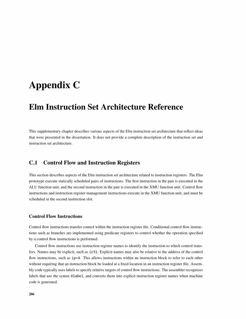
Appendix C
Elm Instruction Set Architecture Reference
This supplementary chapter describes various aspects of the Elm instruction set architecture that reflect ideasthat were presented in the dissertation. It does not provide a complete description of the instruction set andinstruction set architecture.
C.1 Control Flow and Instruction Registers
This section describes aspects of the Elm instruction set architecture related to instruction registers. The Elmprototype execute statically scheduled pairs of instructions. The first instruction in the pair is executed in theALU function unit, and the second instruction in the pair is executed in the XMU function unit. Control flowinstructions and instruction register management instructions execute in the XMU function unit, and must bescheduled in the second instruction slot.
Control Flow Instructions
Control flow instructions transfer control within the instruction register file. Conditional control flow instruc-tions such as branches are implemented using predicate registers to control whether the operation specifiedby a control flow instructions is performed.
Control flow instructions use instruction register names to identify the instruction to which control trans-fers. Names may be explicit, such as ir31. Explicit names may also be relative to the address of the controlflow instructions, such as ip+4. This allows instructions within an instruction block to refer to each otherwithout requiring that an instruction block be loaded at a fixed location in an instruction register file. Assem-bly code typically uses labels to specify relative targets of control flow instructions. The assembler recognizeslabels that use the syntax @label, and converts them into explicit instruction register names when machinecode is generated.
206
[ Supplimentary Section C.1 – Control Flow and Instruction Registers ]
opcode:8 dst:8 rs1:6 extend:10
Figure C.1 – Encoding of Jump Instructions. The dst field encodes the destination, which specifies theinstruction register to which control transfers. The destination may be specified as an absolute destination ora relative destination. Relative targets are resolved when the instruction is loaded into the instruction register.
Jump [ jmp ]
Jump instructions transfer control to the instruction stored in the instruction register specified as the destina-tion. Conditional jumps are implemented using predicate registers to control whether the jump is performed.Control transfers when the predicate in the register specified by rs1 agrees with the predicate condition.
jmp.always <destination>
jmp[.set|.clear] <rs1:pr> <destination:label>
<destination> ← <label>
| ip + <offset:uint8>
| <dst:ir>
The instruction format used to encode jump instructions is shown in Figure C.1. This instruction causes apipeline stall in the instruction fetch (IF) stage when the destination instruction registers has a load pending.The jump instructions implemented in Elm have a single delay slot, and the instruction pair that follows thejump instruction is always executed regardless of whether the jump transfers control.
Loop [ loop ]
Loop instructions provide variants of jump instructions that expose hardware support for implementing loopconstructs.
loop.always <destination:label>
loop[.set|.clear] <rs1:pr> <destination:label> (<count>)
<destination> ← <label>
| ip + <offset:uint8>
| <dst:ir>
<count> ← <rs2>
| <immediate:uint8>
Control transfers when the predicate register specified by rs1 agrees with the predicate condition. If thepredicate is set, indicating that the value zero is stored in the predicate register, the counter is loaded with theloop count encoded in the instruction; otherwise, the counter is decremented and the predicate updated. Thecounter is decremented in the decode stage; the counter is loaded in the write-back stage. The instructionencoded used for loop instructions is the same as the encoding used for jmp instructions and illustrated inFigure C.1.
207

[ Appendix C – Elm Instruction Set Architecture Reference ]
opcode:8 target:6 offset:12 length:6
opcode:8 target:6 rs1:6 offset:6 length:6
Figure C.2 – Encoding of Instruction Load Instructions. The target field specifies the instruction registerat which the instruction block will be loaded. The target may be specified as an absolute position or relativeto the instruction pointer. The address at which the instruction block resides in memory may specified as afixed address encoded in the offset field or as an effective address computed by adding a short offset to thecontents of rs1. The length of the instruction block is encoded in the length field.
Jump and Link [ jal ]
Jump and link operations allow software to implement procedure calls within the instruction registers. Jumpand link operations transfer control to the instruction located at the instruction register specified as the desti-nation and stores the value return instruction pointer address to the link register lr.
jal.always <destination:label>
jal[.set|.clear] <rs1:pr> <destination:label>
<destination> ← <label>
| ip + <offset:uint8>
| <dst:ir>
As with conventional jumps, conditional transfers of control are implemented using predicate registers. Con-trol transfers and the link register is updated when the predicate in the register specified by rs1 agrees withthe predicate condition.
Jump Register [ jr ]
Jump register operations allow software to implement procedure returns within the instruction instructions.Jump register operations transfer control to the instruction in the instruction register specified the value storedin the link register lr.
jr.always <rs2:lr>
jr[.set|.clear] <rs1:pr> <rs2:lr>
As with conventional jumps, conditional transfers of control are implemented using predicate registers. Con-trol transfers and the link register is updated when the predicate in the register specified by rs1 agrees withthe predicate condition.
Jump register operations may be used to implement transfers of control that specify destinations indirectly.For example, some switch statements may be implemented using jump register operations.
208
[ Supplimentary Section C.2 – Control Flow and Instruction Registers ]
Predicate [ pred ]
Conditionally annuls the instruction that issued with the predicate instruction. Both the ALU and XMUfunction units can execute predicate instruction, and the predicate instruction may be paired with any otherinstruction.
pred[.set|.clear] <rs1:pr>
If the predicate value stored in the predicate register specified by rs1 agrees with the predicate condition, theinstruction that issues with the pred instruction is annulled in the decode stage.
Instruction Register Management
The following instructions allow software to load instruction blocks into instruction registers.
Instruction Load [ ild ]
Loads an instruction block to instruction registers.
ild [<destination>] [<address>] (<blocksize:uint6>)
<destination> ← <rd:ir>
| ip + <offset:int>
<address> ← <offset:int>
| <rs1:ar> + <offset:int>
The instructions are loaded at the instruction register specified by the destination field, which may encodeeither an absolute or relative instruction register position. The location of the instruction block can be spec-ified as an absolute address in memory, or it can be specified as a combination of an address register andoffset. The instruction formats used to encode load instructions is illustrated in Figure C.2. The instructionload appears to take effect one cycle after the ild instruction executes.
Instruction Load and Jump [ jld ]
Loads an instruction block into registers and then jumps into the block. The operands and instruction formatsare the same as an instruction load.
jld [<destination>] [<address>] (<blocksize:uint6>)
<destination> ← <rd:ir>
| ip + <offset:int>
<address> ← <offset:int>
| <rs1:ar> + <offset:int>
The jump instruction has a single delay slot, and the instruction load appears to take effect one cycle after thejld instruction executes. Consequently, the instruction pair that follows a jld instruction is always executed,and is read from the instruction registers before the first instructions from the instruction block loads.
209
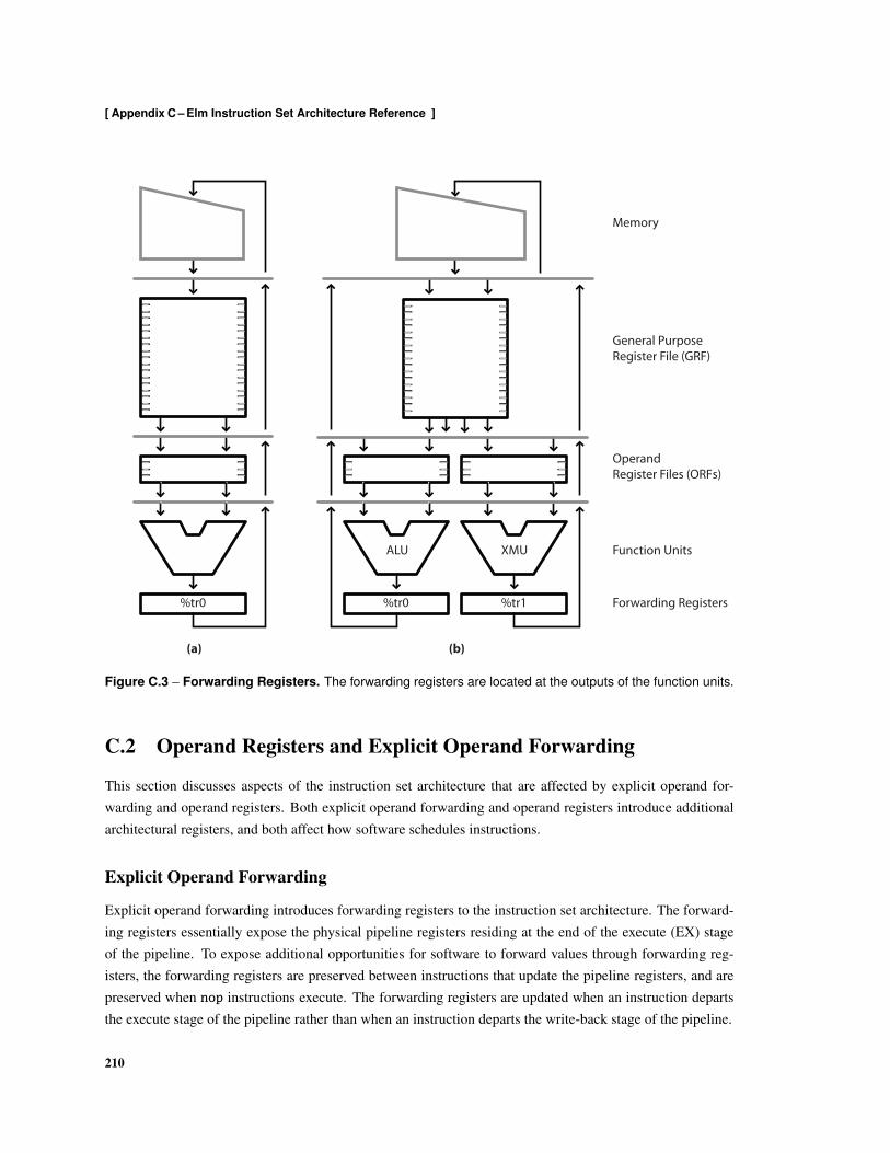
[ Appendix C – Elm Instruction Set Architecture Reference ]
Operand Register Files (ORFs)
General PurposeRegister File (GRF)
Memory
Forwarding Registers
Function Units
%tr0 %tr1%tr0
ALU XMU
(a) (b)
Figure C.3 – Forwarding Registers. The forwarding registers are located at the outputs of the function units.
C.2 Operand Registers and Explicit Operand Forwarding
This section discusses aspects of the instruction set architecture that are affected by explicit operand for-warding and operand registers. Both explicit operand forwarding and operand registers introduce additionalarchitectural registers, and both affect how software schedules instructions.
Explicit Operand Forwarding
Explicit operand forwarding introduces forwarding registers to the instruction set architecture. The forward-ing registers essentially expose the physical pipeline registers residing at the end of the execute (EX) stageof the pipeline. To expose additional opportunities for software to forward values through forwarding reg-isters, the forwarding registers are preserved between instructions that update the pipeline registers, and arepreserved when nop instructions execute. The forwarding registers are updated when an instruction departsthe execute stage of the pipeline rather than when an instruction departs the write-back stage of the pipeline.
210
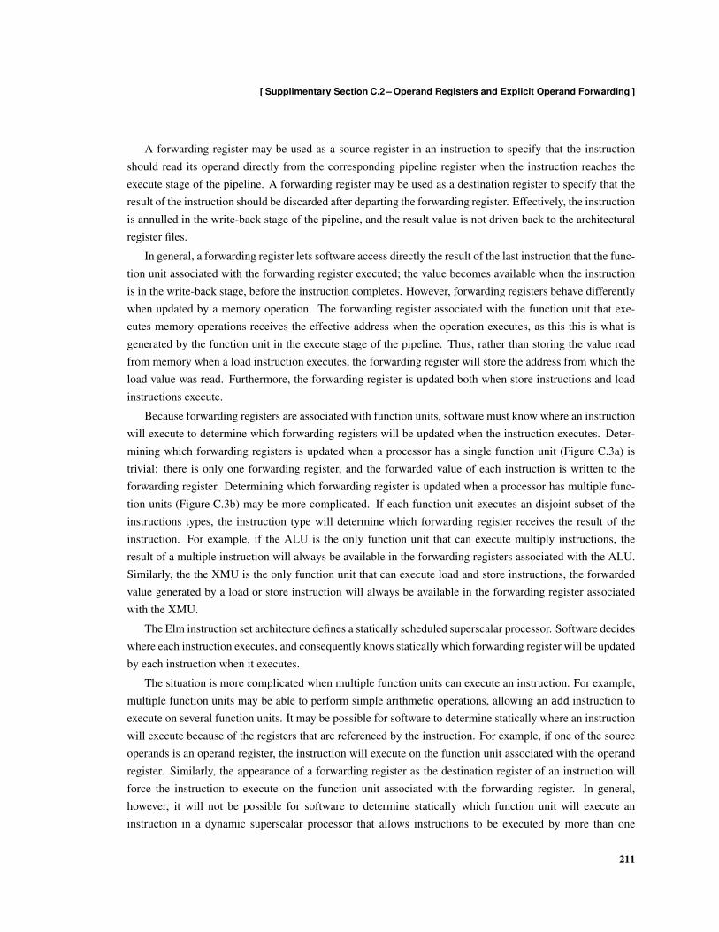
[ Supplimentary Section C.2 – Operand Registers and Explicit Operand Forwarding ]
A forwarding register may be used as a source register in an instruction to specify that the instructionshould read its operand directly from the corresponding pipeline register when the instruction reaches theexecute stage of the pipeline. A forwarding register may be used as a destination register to specify that theresult of the instruction should be discarded after departing the forwarding register. Effectively, the instructionis annulled in the write-back stage of the pipeline, and the result value is not driven back to the architecturalregister files.
In general, a forwarding register lets software access directly the result of the last instruction that the func-tion unit associated with the forwarding register executed; the value becomes available when the instructionis in the write-back stage, before the instruction completes. However, forwarding registers behave differentlywhen updated by a memory operation. The forwarding register associated with the function unit that exe-cutes memory operations receives the effective address when the operation executes, as this this is what isgenerated by the function unit in the execute stage of the pipeline. Thus, rather than storing the value readfrom memory when a load instruction executes, the forwarding register will store the address from which theload value was read. Furthermore, the forwarding register is updated both when store instructions and loadinstructions execute.
Because forwarding registers are associated with function units, software must know where an instructionwill execute to determine which forwarding registers will be updated when the instruction executes. Deter-mining which forwarding registers is updated when a processor has a single function unit (Figure C.3a) istrivial: there is only one forwarding register, and the forwarded value of each instruction is written to theforwarding register. Determining which forwarding register is updated when a processor has multiple func-tion units (Figure C.3b) may be more complicated. If each function unit executes an disjoint subset of theinstructions types, the instruction type will determine which forwarding register receives the result of theinstruction. For example, if the ALU is the only function unit that can execute multiply instructions, theresult of a multiple instruction will always be available in the forwarding registers associated with the ALU.Similarly, the the XMU is the only function unit that can execute load and store instructions, the forwardedvalue generated by a load or store instruction will always be available in the forwarding register associatedwith the XMU.
The Elm instruction set architecture defines a statically scheduled superscalar processor. Software decideswhere each instruction executes, and consequently knows statically which forwarding register will be updatedby each instruction when it executes.
The situation is more complicated when multiple function units can execute an instruction. For example,multiple function units may be able to perform simple arithmetic operations, allowing an add instruction toexecute on several function units. It may be possible for software to determine statically where an instructionwill execute because of the registers that are referenced by the instruction. For example, if one of the sourceoperands is an operand register, the instruction will execute on the function unit associated with the operandregister. Similarly, the appearance of a forwarding register as the destination register of an instruction willforce the instruction to execute on the function unit associated with the forwarding register. In general,however, it will not be possible for software to determine statically which function unit will execute aninstruction in a dynamic superscalar processor that allows instructions to be executed by more than one
211
[ Appendix C – Elm Instruction Set Architecture Reference ]
function unit.
Operand Registers
Operand registers are distributed among a processor’s function units, as depicted in Figure C.3. The distribu-tion of the registers is exposed to software, and the registers in each of the operand register files use differentnames to distinguish the registers. The Elm instruction set architecture refers to the operand registers local tothe arithmetic and logic unit as data registers, and the operand registers local to the load-store unit as addressregisters. The data registers are named dr0 – dr3, and the address registers ar0 – ar3. The register names areneeded to distinguish the registers and reflect typical usage rather than an enforced usage or allocation policy;data registers may be used in address computations and address registers in non-address computations.
Communication between the operand registers and function units is limited. An operand register can onlybe read by its local function unit, not by a remote function unit. However, an operand register can be writtenby any function unit, which allows the function units to communicate through operand registers rather thanmore expensive general-purpose registers. The instruction set architecture exposes the distribution of operandregisters to software, and software is responsible for ensuring that an instruction can access all of its operands.This affects register allocation and instruction scheduling, as software must ensure that instructions will beable to access their operands when they execute. An instruction that attempts to read operand registersassigned to a remote function unit is considered malformed, and the result of the instruction is undefined andmay differ between implementations.
The centralized general-purpose registers back the operand registers, as depicted in Figure C.3. The Elminstruction set architecture refers to the general-purpose registers as general-purpose registers gr0 – gr31.These registers can be accessed by all of the function units. Normally, we would expect the general-purposeregister file would provide enough read ports to allow both instructions to read their operands from thegeneral-purpose registers as the instruction pair passes through the decode stage of the pipeline. However, asignificant fraction of instruction read one or more of their operands from operand registers, which reducesdemand for operand bandwidth at the general-purpose register file. The bandwidth filtering provided by theoperand registers allows the number of read ports at the general-purpose register file to be reduced withoutadversely affecting performance.
The reduction in the number of read ports at the general-purpose register file introduces a structural hazardin the decode stage of the pipeline. Consider, for example, a pair of instructions that execute together andattempt to read four operands from general-purpose registers. With only two read ports to the general-purposeregister file, all four operands cannot be read in a single cycle. Instead, the instruction pair would need tospend two cycles in the decode stage, with two of the four operands read in each cycle. A hardware interlockcould be implemented to detect such conditions.
Rather than providing hardware interlocks, the instruction set architecture implemented in the Elm proto-type exposes the number of read ports directly to software. The instruction set architecture allows an instruc-tion pair to read at most two operands from general-purpose registers. Hardware determines which operandsare read from general-purpose registers and routes the register specifiers and operands accordingly. Software
212
[ Supplimentary Section C.3 – Indexed Registers and Address-Stream Registers ]
is responsible for ensuring that an instruction pair accesses no more than two general-purpose registers, whichaffects instruction scheduling and register allocation.
Forwarding and Interlocks
The introduction of explicit forwarding allows one to consider eliminating conventional hardware forward-ing and instead to rely exclusively on software forwarding. Effectively, software would be responsible forforwarding results back to the function units using the forwarding registers. The operand registers providestorage locations with a one-cycle define-use latency, and the general-purpose registers provide storage lo-cations with a two-cycle define-use latency. However, relying exclusively on software to forward valuescomplicates scheduling and increases the number of nop instructions that need to be scheduled to ensure thatoperands are available where subsequent instructions expect them. It eliminates the hardware that tracks de-pendencies, which saves energy, but increases code size and results in more instructions being issued from theinstruction registers. The Elm architecture provides hardware forwarding and interlocks because the reduc-tion in the energy consumed loading and issuing instructions exceeded the energy consumed in the additionaldata-path control logic.
C.3 Indexed Registers and Address-Stream Registers
This section describes aspects of the instruction set architecture that relate to the index registers and address-stream registers.
Index and Indexed Registers
Index registers xp0 – xp3 store pairs of pointers that let software access the indexed registers indirectly.Indexed registers xr0 – xr2047 extend the general-purpose registers; indexed registers xr0 – xr31 are thesame physical registers as general-purpose registers gr0 – gr31. The Elm instruction set architecture allowsa processor to implement between 32 and 2048 indexed registers. Figure C.4 illustrates the format used totransfer 64-bit index register values between memory and the index registers.
Each index register provides independent read and write pointers and independent read and write updateincrements. When an instruction specifies an index register appears as a source register, the read pointer valuestored in the index register is used to read the operand from the indexed registers; the read pointer is updatedin the decode stage after the operand is read from the indexed registers. When an instruction specifies anindex register as a destination register, the write pointer value stored in the index register specifies the indexregister to which the result is written; the write pointer is updated in the write-back stage after the result ofthe operation is written to the destination indexed register. Should an index register appear in multiple sourceoperand positions within an instruction pair, the read pointer is only updated once. Similarly, should anindex register appear in multiple destination register positions within an instruction pair, the write pointer isonly updated once. Software assigns each index register a range of indexed registers, and the read and writepointers are automatically adjusted to iterate through the assigned range of registers. Dedicated hardware
213
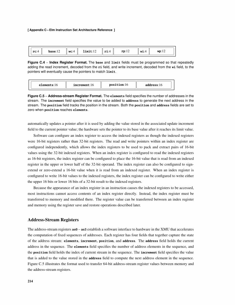
[ Appendix C – Elm Instruction Set Architecture Reference ]
rc:4 base:12 wc:4 limit:12 ri:4 rp:12 wi:4 wp:12
Figure C.4 – Index Register Format. The base and limit fields must be programmed so that repeatedlyadding the read increment, decoded from the ri field, and write increment, decoded from the wi field, to thepointers will eventually cause the pointers to match limit.
elements:16 increment:16 position:16 address:16
Figure C.5 – Address-stream Register Format. The elements field specifies the number of addresses in thestream. The increment field specifies the value to be added to address to generate the next address in thestream. The position field tracks the position in the stream. Both the position and address fields are set tozero when position reaches elements.
automatically updates a pointer after it is used by adding the value stored in the associated update incrementfield to the current pointer value; the hardware sets the pointer to its base value after it reaches its limit value.
Software can configure an index register to access the indexed registers as though the indexed registerswere 16-bit registers rather than 32-bit registers. The read and write pointers within an index register areconfigured independently, which allows the index registers to be used to pack and extract pairs of 16-bitvalues using the 32-bit indexed registers. When an index register is configured to read the indexed registersas 16-bit registers, the index register can be configured to place the 16-bit value that is read from an indexedregister in the upper or lower half of the 32-bit operand. The index register can also be configured to sign-extend or zero-extend a 16-bit value when it is read from an indexed register. When an index register isconfigured to write 16-bit values to the indexed registers, the index register can be configured to write eitherthe upper 16 bits or lower 16 bits of a 32-bit result to the indexed registers.
Because the appearance of an index register in an instruction causes the indexed registers to be accessed,most instructions cannot access contents of an index register directly. Instead, the index register must betransferred to memory and modified there. The register value can be transferred between an index registerand memory using the register save and restore operations described later.
Address-Stream Registers
The address-stream registers as0 – as3 establish a software interface to hardware in the XMU that acceleratesthe computation of fixed sequences of addresses. Each register has four fields that together capture the stateof the address stream: elements, increment, position, and address. The address field holds the currentaddress in the sequence. The elements field specifies the number of address elements in the sequence, andthe position field holds the index of current stream in the sequence. The increment field specifies the valuethat is added to the value stored in the address field to compute the next address element in the sequence.Figure C.5 illustrates the format used to transfer 64-bit address-stream register values between memory andthe address-stream registers.
214
[ Supplimentary Section C.3 – Indexed Registers and Address-Stream Registers ]
Vector Memory Operations
Vector memory operations transfer multiple elements between indexed registers and memory. Vector mem-ory operations are similar to convention memory operations except that each vector memory operation trans-fers multiple elements. Vector memory operations provide the same semantics as executing an equivalentsequence of scalar load and store instructions. The number of elements that a vector memory operation trans-fers is specified by software and encoded in the vector memory instruction. Address-stream registers can beused to generate the effective memory addresses at from which elements are loaded and to which elementsare stored.
Vector Load — ld.v Vector load operations load multiple elements from memory to indexed registers. Vectorload operations use the following assembly syntax.
ld.v <rd:xp> < address> ( <elements:uint6> )
<address> := [ <offset:int12> ]
| [ <rs1> + <offset:int6> ]
| [ <rs1> + <rs2> ]
The destination register specifies the index register that generates the sequence of indexed registers to whichthe elements are loaded. The value of elements encodes the number of elements that will be loaded. Exceptwhen an address-stream register appears in the address fields, the effective address computed from the con-tents of the source registers determines the address of the first element in the vector transfer. The address ofsubsequent elements is computed by incrementing the effective address. For example, the following instruc-tion loads 4 elements from consecutive memory locations starting at effective address computed by adding16 to the content of ar1.
ld.v xp0 [ar1+16] (4)
The following sequence of 4 scalar load operations produces the same effect as the vector load operation.
ld xp0 [ar1+16]
ld xp0 [ar1+17]
ld xp0 [ar1+18]
ld xp0 [ar1+19]
When an address-stream register is used to compute the effective address, the address-stream registeris updated after each element is loaded and the effective address of the next element is computed usingthe updated address-stream register value. The address-stream registers allow vector memory operations toaccess memory with strides other than one. For example, the following vector memory operations loads 4elements from the memory locations specified by the address sequence produced by adding the contents ofar1 to the address stream produced by as0.
ld.v xp0 [ar1+as0] (4)
The following sequence of 4 scalar load operations produces the same effect as the vector load operation.
215
[ Appendix C – Elm Instruction Set Architecture Reference ]
ld xp0 [ar1+as0]
ld xp0 [ar1+as0]
ld xp0 [ar1+as0]
ld xp0 [ar1+as0]
Vector Store — st.v Vector store operations store multiple elements from indexed registers to memory.Vector store operations use an assembly syntax similar to vector load operations.
st.v <rs:xp> < address> ( <elements:uint6> )
<address> := [ <offset:int12> ]
| [ <rs1> + <offset:int6> ]
| [ <rs1> + <rs2> ]
The source register specifies the index register that generates the sequence of indexed registers to be stored.
Though vector memory operations appear to execute as atomic operations, the memory operations thattransfer individual elements may be interleaved with memory operations from other processors.
Saving and Restoring Index and Address-stream Registers
Usually, an instruction that references an index register or address-stream registers modifies the state of theregister when it executes. The instruction set provides two operations, save and restore, to let software accessregisters such as the index registers and address-stream registers without modifying the registers and affectingthe processor state.
In addition to allowing software to save and restore the register state of the processor, the save and restoreoperations are used to configure the index and address-stream registers. The save and restore operations areeffectively distinguished store and load instructions that transfer 64-bit values between memory and registers.When used to store an index register or address-stream register, a save operation transfers the 64-bit valuestored in the register to memory without affecting the state of the register. Software uses save operationsto store the state of the index and address-stream registers when storing the state of a processor to memory.When used to load an index register or address-stream register, a restore operations transfers a 64-bit valuefrom memory to the destination register. restore the register state of a processor from memory. Softwareuses restore instructions to initialize the index and address-stream registers, and to restore the state of indexand address-stream registers when restoring the state of a processor from memory. The save and restoreinstructions are described below.
Save Register — st.save Saves register rd to the effective address computed when the instruction executes.The save operation is effectively a store operation that will transfer an entire register regardless of its size tomemory without affecting the state of the saved register.
st.save <rd> <address>
<address> := [ <offset:uint18> ]
| [ <rs1> + <offset:int12> ]
| [ <rs1> + <rs2> ]
216

[ Supplimentary Section C.4 – Ensembles and Processor Corps ]
When register rd is a 32-bit register, the instruction stores the 32-bit value contained in rd to the effectivememory address; when register rd is a 64-bit register, the save operation stores the 64-bit value contained inrd to memory. When register rd is an index register, the save operation stores the state of the index registerto memory. The state of rd is not affected by the execution of the operation.
Restore Register — ld.rest Restores register rd from the effective address computed when the instructionexecutes. The restore operation is effectively a load operation that transfers an entire register regardless of itssize from memory without otherwise affecting the state of the restored register.
ld.rest <rd> <address>
<address> := [ <offset:uint18> ]
| [ <rs1> + <offset:int12> ]
| [ <rs1> + <rs2> ]
When register rd is a 32-bit register, the operation loads the 32-bit stored at the effective address from memoryto rd; when register rd is a 64-bit register, the operation loads the 64-bit value stored at the effective memoryaddress to rd. When register rd is an index register, the restore operation loads the state of the index registerfrom memory. The state of rd is updated to reflect the load operation, but is not subsequently modified.
C.4 Ensembles and Processor Corps
This section describes aspects of the Elm instruction set architecture that reflect the Ensemble organizationof processors, memory, and interconnect.
Message Registers
Message registers mr0 – mr7 provide names for accessing the ingress and egress ports to the local commu-nication fabric. A message register may be used where a general-purpose register is permitted as operandsource and where a general-purpose register is permitted as a result destination. The synchronization bit as-sociated with a message register is set to indicate the register is full when the message register is written, andit is set to indicate the register is empty when the register is read. The processor stalls when an instructionattempts to read a message register that is marked as empty until its synchronization bit indicates the registeris full. The processor similarly stalls when an instruction attempts to write a message register that is markedas full until its synchronization bit indicates that the register is empty.
The synchronization bits associated with the message registers may be accessed through the processorcontrol word in the processor status register. Software may inspect the synchronization bits to determinewhether a message register is marked as full or empty, and may update the synchronization bits to markmessage registers as full or empty without accessing the message registers. In some cases, software mayprefer to inspect the synchronization bits to check whether a message register is empty before accessing it toavoid stalling the processor when the message register is empty. The synchronization bits may be transferredbetween memory and the processor status register using save and restore operations.
217
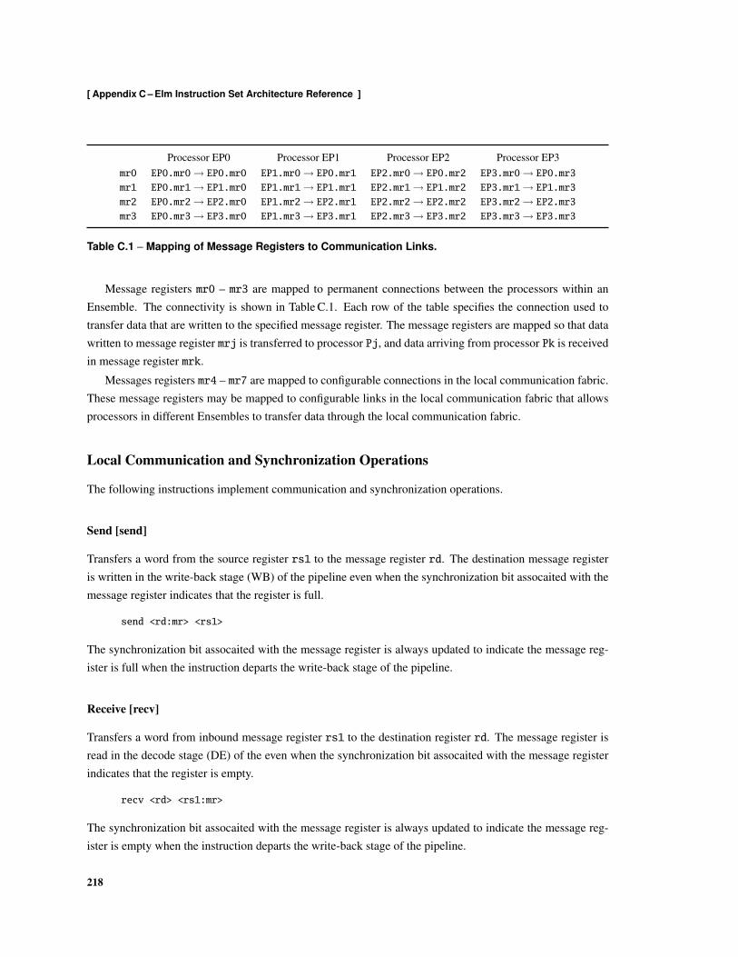
[ Appendix C – Elm Instruction Set Architecture Reference ]
Processor EP0 Processor EP1 Processor EP2 Processor EP3mr0 EP0.mr0→ EP0.mr0 EP1.mr0→ EP0.mr1 EP2.mr0→ EP0.mr2 EP3.mr0→ EP0.mr3
mr1 EP0.mr1→ EP1.mr0 EP1.mr1→ EP1.mr1 EP2.mr1→ EP1.mr2 EP3.mr1→ EP1.mr3
mr2 EP0.mr2→ EP2.mr0 EP1.mr2→ EP2.mr1 EP2.mr2→ EP2.mr2 EP3.mr2→ EP2.mr3
mr3 EP0.mr3→ EP3.mr0 EP1.mr3→ EP3.mr1 EP2.mr3→ EP3.mr2 EP3.mr3→ EP3.mr3
Table C.1 – Mapping of Message Registers to Communication Links.
Message registers mr0 – mr3 are mapped to permanent connections between the processors within anEnsemble. The connectivity is shown in Table C.1. Each row of the table specifies the connection used totransfer data that are written to the specified message register. The message registers are mapped so that datawritten to message register mrj is transferred to processor Pj, and data arriving from processor Pk is receivedin message register mrk.
Messages registers mr4 – mr7 are mapped to configurable connections in the local communication fabric.These message registers may be mapped to configurable links in the local communication fabric that allowsprocessors in different Ensembles to transfer data through the local communication fabric.
Local Communication and Synchronization Operations
The following instructions implement communication and synchronization operations.
Send [send]
Transfers a word from the source register rs1 to the message register rd. The destination message registeris written in the write-back stage (WB) of the pipeline even when the synchronization bit assocaited with themessage register indicates that the register is full.
send <rd:mr> <rs1>
The synchronization bit assocaited with the message register is always updated to indicate the message reg-ister is full when the instruction departs the write-back stage of the pipeline.
Receive [recv]
Transfers a word from inbound message register rs1 to the destination register rd. The message register isread in the decode stage (DE) of the even when the synchronization bit assocaited with the message registerindicates that the register is empty.
recv <rd> <rs1:mr>
The synchronization bit assocaited with the message register is always updated to indicate the message reg-ister is empty when the instruction departs the write-back stage of the pipeline.
218

[ Supplimentary Section C.4 – Ensembles and Processor Corps ]
Barrier [barrier]
The barrier instruction provides a barrier synchronization mechanism to processors within an Ensemble. Theprocessors participating in the barrier may be specified as a list of processor identifiers, which is encoded asa bit-vector in the immediate field of the instruction, or may be specified as a bit-vector stored in a registeroperand.
barrier <group>
<group> ← ( <processors-list:immediate> )
| <rs1>
A processor signals that it has reached a barrier when the barrier instruction enters the write-back stage (WB)and there are no outstanding memory transactions. This ensures that all preceding instructions have clearedthe pipeline and all memory operations have committed. The processor stalls with the barrier instructionin the write-back stage until all other processors participating in the barrier similarly signal that they havereached the barrier. The barrier instruction is immediately retired, and the processor continues to executesubsequent instructions.
Load Barrier [ld.b]
The load barrier operation combines a barrier and a load operation to provide a synchronized load operation.This ensures that a set of processors perform the load at the same time, and may be used to ensure thataccesses by different processors to shared memory locations are coordinated.
ld.b <rd> < address> [ <processor-list> ]
<address> ← [ <offset:int12> ]
| [ <rs1> + <offset:int6> ]
| [ <rs1> + <rs2> ]
The processor list names the processors participating in the barrier operation. The load barrier operation maybe used to synchronized loads from different processors to the same memory location to ensure that memoryis accessed once and the result broadcast to multiple processors.
Store Barrier[st.b]
The store barrier operation combines a barrier and a store operation to provide a synchronized load operation.This ensures that a set of processors perform the load at the same time, and may be used to ensure thataccesses by different processors to shared memory locations are coordinated.
st.b <rd> < address> [ <processor-list> ]
<address> ← [ <offset:int12> ]
| [ <rs1> + <offset:int6> ]
| [ <rs1> + <rs2> ]
The processor list names the processors participating in the barrier operation. The store barrier operationshould not be used to synchronize stores from multiple processors to the same memory location. Which
219

[ Appendix C – Elm Instruction Set Architecture Reference ]
processor successfully stores its value to memory will depend on how an implementation resolves the writeconflict.
Processor Corps and Instruction Register Pools
Processors in a processor corps execute a common instruction stream. The execution model differs suffi-ciently from conventional single-instruction multiple-data execution models to justify some attention. In-structions are fetched from the shared instruction register pool and are issued to all of the processors in thecorps. The processors execute the instructions independently, and may access different registers and differentnon-contiguous memory locations. Because the shared instruction register pool is formed by aggregatingthe instruction registers of processors participating in the processor corps, the shared instruction registers arephysically distributed with the processors. The shared instruction registers appear to be accessed as thoughthere were 4 instruction register banks. Each processor is responsible for fetching and issuing those sharedinstructions that reside in its local instruction registers. This improves instruction fetch and issue locality, andreduces the number of control signals that pass between the processors. Dedicated hardware orchestrates thefetching and issuing of shared instructions so that the process is transparent to software. Each processor isresponsible for loading any shared instructions that reside in its local instruction registers. This keeps instruc-tion load bandwidth local to each instruction register and ensures that all instruction load operates originatelocally, which simplifies the design of the instruction load unit. It also increases the effective instruction loadbandwidth that is available when loading shared instructions, as the processors in a corps can concurrentlyload shared instructions in parallel. However, software must explicitly schedule instruction load operationsthat load shared instructions so that the correct processor performs the load.
The organization of the instruction registers in an instruction register pool is illustrated in Figure C.6.Because a shared instruction register pool is formed by aggregating multiple processors’ instruction registers,the shared instruction registers are physically distributed among the processors in a processor corps. Instruc-tion registers in an instruction register pool are addressed using extended instruction register identifiers. Theextended identifiers are formed by concatenating the processor identifier and its local instruction register ad-dress, as illustrated in Figure C.7. This encoding maps instruction registers in an instruction register file toadjacent identifiers, and allows extended instruction register identifiers to encode instruction register localityby exposing the physical distribution of instruction registers.
Loading Shared Instructions
To allow all operations that access instruction register file to be performed locally, each processor in a corps isresponsible for managing its local instruction registers. For example, processor EP1 is responsible for issuinginstructions from shared instruction registers sir64 – sir127, and is responsible for loading instructions toshared instruction registers sir64 – sir127. Shared instruction registers are loaded using instruction loadoperations to load instruction registers locally. The shared instruction register identifier is determined bywhere the instruction load operation executes and the instruction register address specified by the operation.For example, an instruction load operation that transfers instruction to instruction registers ir8 – ir16 will
220
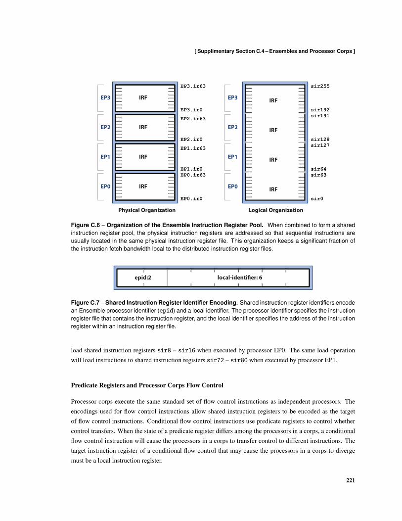
[ Supplimentary Section C.4 – Ensembles and Processor Corps ]
EP0.ir0
EP0.ir63EP1.ir0
EP1.ir63
EP2.ir0
EP2.ir63
EP3.ir0
EP3.ir63
sir0
sir63sir64
sir127sir128
sir191sir192
sir255
EP3
EP2
EP1
EP0
EP3
EP2
EP1
EP0IRF
IRF
IRF
IRF
IRF
IRF
IRF
IRF
Physical Organization Logical Organization
Figure C.6 – Organization of the Ensemble Instruction Register Pool. When combined to form a sharedinstruction register pool, the physical instruction registers are addressed so that sequential instructions areusually located in the same physical instruction register file. This organization keeps a significant fraction ofthe instruction fetch bandwidth local to the distributed instruction register files.
local-identi!er: 6epid:2
Figure C.7 – Shared Instruction Register Identifier Encoding. Shared instruction register identifiers encodean Ensemble processor identifier (epid) and a local identifier. The processor identifier specifies the instructionregister file that contains the instruction register, and the local identifier specifies the address of the instructionregister within an instruction register file.
load shared instruction registers sir8 – sir16 when executed by processor EP0. The same load operationwill load instructions to shared instruction registers sir72 – sir80 when executed by processor EP1.
Predicate Registers and Processor Corps Flow Control
Processor corps execute the same standard set of flow control instructions as independent processors. Theencodings used for flow control instructions allow shared instruction registers to be encoded as the targetof flow control instructions. Conditional flow control instructions use predicate registers to control whethercontrol transfers. When the state of a predicate register differs among the processors in a corps, a conditionalflow control instruction will cause the processors in a corps to transfer control to different instructions. Thetarget instruction register of a conditional flow control that may cause the processors in a corps to divergemust be a local instruction register.
221
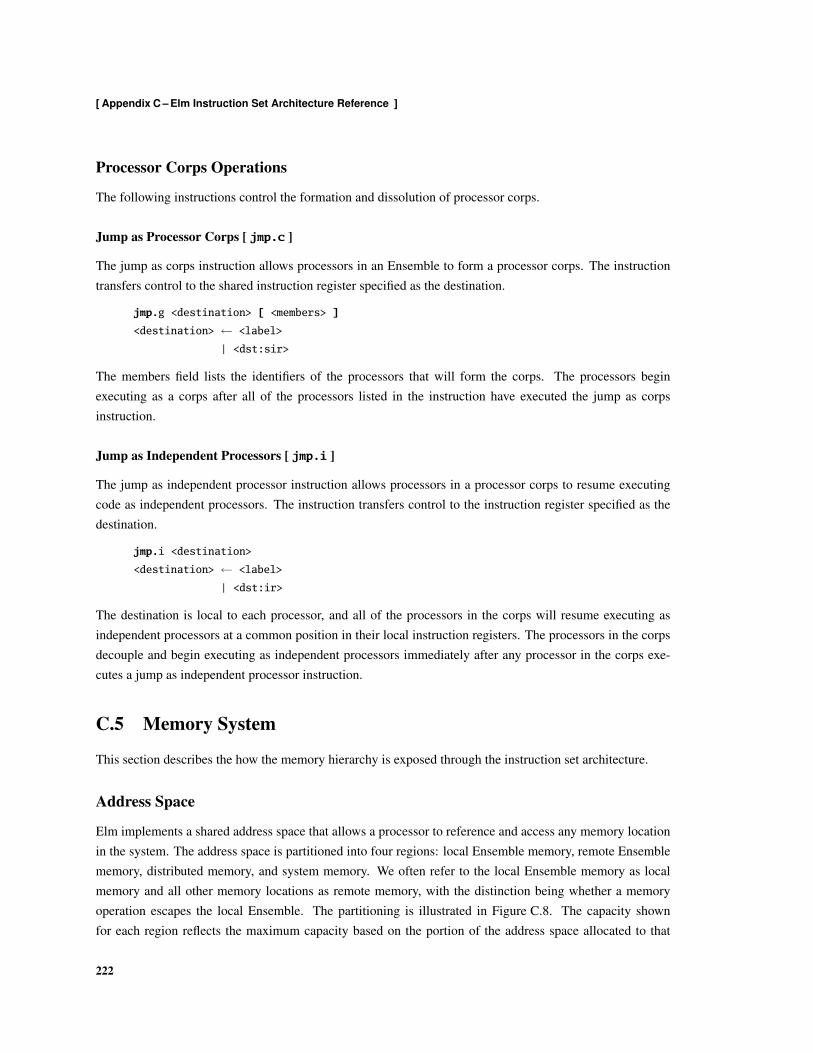
[ Appendix C – Elm Instruction Set Architecture Reference ]
Processor Corps Operations
The following instructions control the formation and dissolution of processor corps.
Jump as Processor Corps [ jmp.c ]
The jump as corps instruction allows processors in an Ensemble to form a processor corps. The instructiontransfers control to the shared instruction register specified as the destination.
jmp.g <destination> [ <members> ]
<destination> ← <label>
| <dst:sir>
The members field lists the identifiers of the processors that will form the corps. The processors beginexecuting as a corps after all of the processors listed in the instruction have executed the jump as corpsinstruction.
Jump as Independent Processors [ jmp.i ]
The jump as independent processor instruction allows processors in a processor corps to resume executingcode as independent processors. The instruction transfers control to the instruction register specified as thedestination.
jmp.i <destination>
<destination> ← <label>
| <dst:ir>
The destination is local to each processor, and all of the processors in the corps will resume executing asindependent processors at a common position in their local instruction registers. The processors in the corpsdecouple and begin executing as independent processors immediately after any processor in the corps exe-cutes a jump as independent processor instruction.
C.5 Memory System
This section describes the how the memory hierarchy is exposed through the instruction set architecture.
Address Space
Elm implements a shared address space that allows a processor to reference and access any memory locationin the system. The address space is partitioned into four regions: local Ensemble memory, remote Ensemblememory, distributed memory, and system memory. We often refer to the local Ensemble memory as localmemory and all other memory locations as remote memory, with the distinction being whether a memoryoperation escapes the local Ensemble. The partitioning is illustrated in Figure C.8. The capacity shownfor each region reflects the maximum capacity based on the portion of the address space allocated to that
222
[ Supplimentary Section C.5 – Memory System ]
Local Ensemble[interleaved]
Local Ensemble [contiguous]
Remote Ensemble[interleaved]
Remote Ensemble[contiguous]
Distributed Memory
System Memory
0x00000000
0x00007FFF0x00008000
0x0000FFFF
128KB
128KB
0x00010000
0x3FFFFFFF
0x800000000x7FFFFFFF
0x40000000
0xFFFFFFFF
1,024 MB
2,048 MB
8,096 MBSystem Memory Region
DistributedMemory Region
Remote EnsembleMemory Region
Local EnsembleMemory Region
Figure C.8 – Address Space.
memory region, and does not necessarily reflect the provisioned capacity of the memories in any particularElm system.
Local Ensemble Memory Region
The local Ensemble memory region provides a consistent mechanism for naming local Ensemble memorythat is independent of where a thread is mapped in the system. Addresses in the local Ensemble addressspace always map to memory locations in the local Ensemble memory. This simplifies the generation ofposition independent code that will execute correctly regardless of where it executes. However, addresses inthis range refer to different physical memory locations within different Ensembles, and addresses within thelocal Ensemble region have no meaning beyond of the Ensemble in which they are generated. Consequently,these addresses are commonly used for objects that are private and local to a thread, such as stacks and
223

[ Appendix C – Elm Instruction Set Architecture Reference ]
0x000000000x000000010x00000002
0x000020000x000020010x00002002
0x000030000x000030010x00003002
0x00002FFF 0x00003FFF0x00002FFE 0x00003FFE
0x00000FFF0x00000FFE
0x000010000x000010010x00001002
0x00002FFF0x00002FFE
0x00000000 0x000000020x00000004
0x000000030x00000007
0x00003FFE 0x00003FFF0x00003FFA 0x00003FFB
0x00003FFC0x00003FF8
0x00000001
0x00003FFD0x00003FF9
0x00000005 0x000000060x00000008 0x0000000B0x00000009 0x0000000A
[ Bank 0 ] [ Bank 1 ] [ Bank 2 ] [ Bank 3 ]
[ Bank 0 ] [ Bank 1 ] [ Bank 2 ] [ Bank 3 ]
Contiguous
Interleaved
Figure C.9 – Memory Interleaving. Memory operations that transfer data between a contiguous region ofmemory and an interleaved region of memory can be used to implement conversions between structure-of-array and array-of-structure data object layouts.
temporaries.
Memory Interleaving
As shown in Figure C.8, each location in the local Ensemble memory appears twice in the local Ensembleaddress range: once with the memory banks contiguous, and once with the memory banks interleaved. In thecontiguous address range, address bits in the middle of the address select the bank; the specific bits depend onthe capacity of the Ensemble memory. In the interleaved address range, the least significant address bits selectthe bank. The difference is illustrated in Figure C.9. The contiguous and interleaved address ranges map tothe same physical memory, so each physical memory word is addressed by two different local addresses.
The contiguous addressing scheme is useful when independent threads are mapped to an Ensemble. Athread may be assigned one of the local memory banks, and any data it accesses may be stored in its assignedmemory bank. This avoids bank conflicts when threads within an Ensemble attempt to access the localmemory concurrently, which improves performance and allows for more predictable execution. Becauseconsecutive addresses map to the same memory bank, all of the data accessed by the thread resides within a
224

[ Supplimentary Section C.5 – Memory System ]
contiguous address range, and no special addressing is required to avoid bank conflicts.
The interleaved addressing scheme is useful when collaborative threads are mapped to an Ensemble. Ad-jacent addresses are mapped to different banks, and accesses to consecutive addresses are distributed acrossthe banks. This allows data transfers between local Ensemble memory and remote memory to use consecutiveaddresses while distributing the data across multiple the banks, which improves bandwidth utilization whenthe memories are accessed by the processors within the Ensemble.
Remote Ensemble Memory Region
The remote Ensemble memory region comprises the aggregate of the Ensemble memory in a system. Ad-dresses within this region have meaning throughout the system, and the remote Ensemble memory regioneffectively corresponds to the system view of all of the Ensemble memory. Addresses within the remoteEnsemble address range have meaning both inside and outside of an Ensemble. The local Ensemble memoryalso appears in the remote Ensemble memory address range; where it appears depends on the global addressassigned to the Ensemble. This convention provides a consistent mechanism for two Ensembles to namea memory location that resides within on of their Ensemble memories. Like the local Ensemble memory,each remote Ensemble memory appears twice: once in the continuous address range, and once in the in-terleaved address range. The interleaved addresses map to physical banks such that banks are interleavedwithin Ensembles but not across Ensembles, and the addresses assigned to an Ensemble in the interleavedand contiguous ranges are offset by a constant displacement.
Distributed Memory Region
The distributed memory is mapped into the distributed memory address range. Addresses within this rangehave meaning throughout the system, and are used to directly access memory locations in the DistributedMemories. When part of the distributed memory operates as a cache, memory accesses that attempt to accessthe distributed memory as though it were software-managed will access the cache control data instead. Loadsreturn the tag and status information, and stores allow the tag and status information to be modified.
System Memory Region
The system memory region includes off-chip memory and memory mapped input-output regions. An Elmsystem may have multiple memory channels and independent memory controllers to provide additional par-allelism within the memory system.
Software-Allocated Hardware-Managed Caches
Remote Memory Operations
The instruction set distinguishes between memory operations that access local memory and remote memory.The distinction allows software to indicate which memory operations require only local hardware resources,
225

[ Appendix C – Elm Instruction Set Architecture Reference ]
and allows the hardware to optimize the handling of local memory operations. Both local and remote memoryoperations may access local memory. However, local memory operations may only access local memory,whereas remote memory operations may access any memory location. Remote memory operations use anon-chip interconnection network to transfer data between the Ensemble and remote memories. The networkinterface at the remote memory provides a serialization point. Remote memory operations that access thelocal Ensemble memory as a remote memory access the local memory through the network interface; thisensures that the operations are serialized with respect to other concurrent remote memory accesses.
Remote Load [ ld.r ]
Transfer data from memory to the destination register. The operation stalls in the execute (EX) stage if thenetwork interface is unavailable. The operation always stalls in the write-back (WB) stage until the load valueis received.
ld.r <rd:gr> <rs1> <rs2>
Remote Store [ st.r ]
Transfers data from a register to memory. The operation stalls in the execute (EX) stage if the networkinterface is unavailable. The operation stalls in the write-back (WB) stage until a message indicating that thestore has completed is returned to the processor. This ensures that sequences of stores become visible to otherprocessors in the order in which the stores execute.
st.r <rd:gr> <rs1> <rs2>
Cached Remote Load [ ld.c ]
The operation will stall in the execute (EX) stage if the network interface is unavailable. The operation alwaysstalls in the write-back (WB) stage until the load value is received.
ld.c <rd:gr> <rs1> <rs2>
Cached Remote Store [ st.c ]
Remote cached store. The operation will stall in the execute (EX) stage if the network interface is unavailable.The operation stalls in the write-back (WB) stage until the message indicating that the store has completedis returned to the processor. This ensures that sequences of stores become visible to other processors in theorder in which the stores execute.
st.c <rd:gr> <rs1> <rs2>
226
[ Supplimentary Section C.5 – Memory System ]
Decoupled Remote Load [ ld.r.d ]
Non-blocking remote load. A presence flag associated with the destination register, which must be a GR orXR, tracks when the load value arrives. Reading the register causes the processor to stall until the load valueis received. Writing the register sets the presence flag and kills the load operation (the load value is discardedwhen it arrives).
ld.r.d <rd:gr> <rs1> <rs2>
Decoupled Remote Store [ st.r.d ]
Non-blocking remote store. Like a remote store, except the processor does not wait for the message indicatingthat the store has completed to be returned.
st.r.d <rd:gr> <rs1> <rs2>
Decoupled Cached Remote Load [ ld.c.d ]
Non-blocking cached remote load. A presence flag associated with the destination register, which must bea GR or XR, tracks when the load value arrives. Reading the register causes the processor to stall until theload value is received. Writing the register sets the presence flag and kills the load operation (the load valueis discarded when it arrives).
ld.c.d <rd:gr> <rs1> <rs2>
Decoupled Cached Remote Load [ st.c.d ]
Non-blocking cached remote store. Like a remote store, except the processor does not wait for the messageindicating that the store has completed to be returned.
st.c.d <rd:gr> <rs1> <rs2>
Atomic Compare-and-Swap [ atomic.cas ]
The address is specified by rs1, the comparison value by rs2, and the update value by rs3. The value at thememory location is returned to rd.
atomic.cas <rd> [ <rs1> ] <rs2> <rs3>
Atomic Fetch-and-Add [ atomic.fad ]
The memory location is specified by rs1. The current value at the memory location referenced by rs1 isreturned to rd. The value of register rs2 is added to the contents of the memory location specified by rs1.If the sum is equal to the value of register rs3, the memory location is updated to 0. Otherwise, the memorylocation is updated to the sum.
227
[ Appendix C – Elm Instruction Set Architecture Reference ]
atomic.fad <rd> [ <rs1> ] <rs2> <rs3>
Block Memory Operations
Block memory operations move contiguous blocks of memory through the memory system.
Block Get [ get ]
Transfers a block of memory from a remote memory location to a local memory location.
get [ <dst> ] [ <src> ] ( <size> )
Block Put [ put ]
Transfers a block of memory from a local memory location to a remote memory location.
put [ <dst> ] [ <src> ] ( <size> )
Block Move [ move ]
Transfers a block of memory from a remote memory location to a remote memory location.
move [ <dst> ] [ <src> ] ( <size> )
Stream Memory Operations
Stream memory operations transfer blocks of instructions and data through memory. A stream memoryoperation transfers a set of records, which are contiguous memory blocks, through the memory system.
Stream Descriptors
Streams are composed of sequences of fixed-length records. A stream descriptor describes the layout ofa stream in memory, specifically where the records comprising the stream are located. Effectively, streamdescriptors provide a compact representation with which software can efficiently describe a sequence ofaddresses to hardware. Hardware uses stream descriptors to calculate the addresses of the records whenstream operations move records through the memory system. A stream descriptor provides the followinginformation.
record-size — The size of each record in words.
stream-size — The number of records in the stream.
stride — The stride used to calculate the address of consecutive records.
index-address — The address at which an index vector resides. The entries of the index vector specify theoffset of each record in the stream.
228
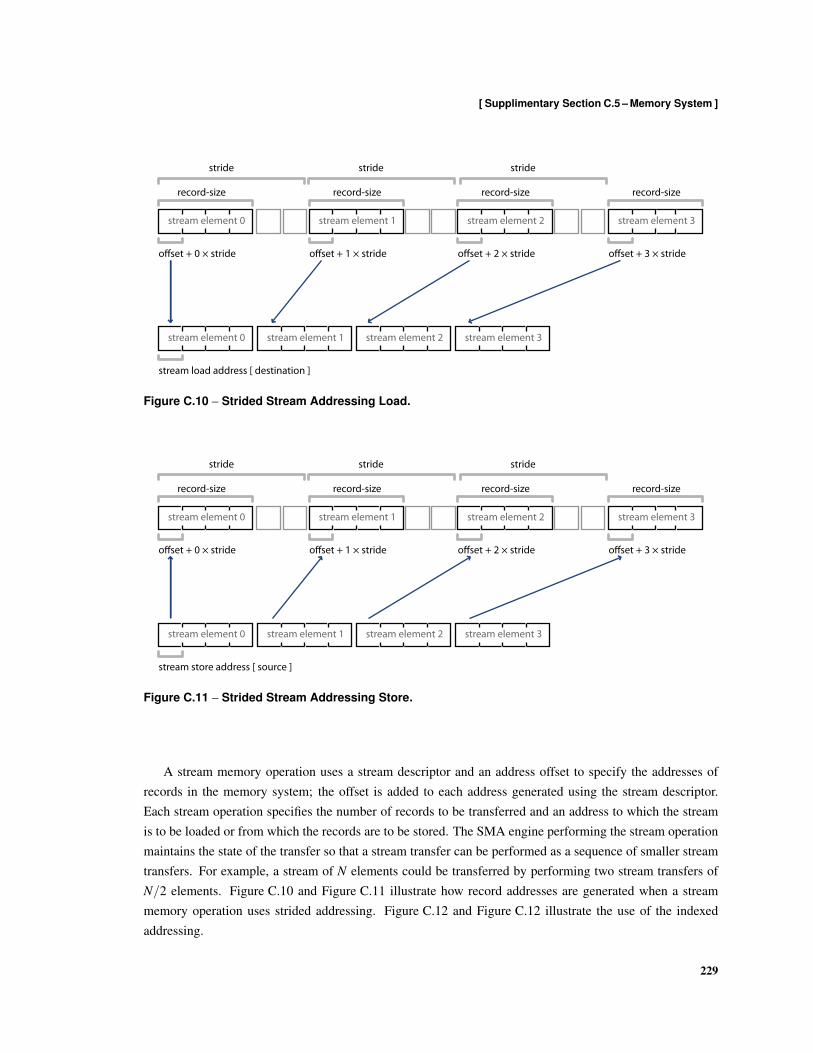
[ Supplimentary Section C.5 – Memory System ]
record-size
stride
record-size
o!set + 0 " stride o!set + 1 " stride
stream element 0 stream element 1
stream element 0 stream element 1
record-size
o!set + 2 " stride
stream element 2
stream element 2
stream load address [ destination ]
record-size
o!set + 3 " stride
stream element 3
stream element 3
stride stride
Figure C.10 – Strided Stream Addressing Load.
record-size
stride
record-size
o!set + 0 " stride o!set + 1 " stride
stream element 0 stream element 1
stream element 0 stream element 1
record-size
o!set + 2 " stride
stream element 2
stream element 2
stream store address [ source ]
record-size
o!set + 3 " stride
stream element 3
stream element 3
stride stride
Figure C.11 – Strided Stream Addressing Store.
A stream memory operation uses a stream descriptor and an address offset to specify the addresses ofrecords in the memory system; the offset is added to each address generated using the stream descriptor.Each stream operation specifies the number of records to be transferred and an address to which the streamis to be loaded or from which the records are to be stored. The SMA engine performing the stream operationmaintains the state of the transfer so that a stream transfer can be performed as a sequence of smaller streamtransfers. For example, a stream of N elements could be transferred by performing two stream transfers ofN/2 elements. Figure C.10 and Figure C.11 illustrate how record addresses are generated when a streammemory operation uses strided addressing. Figure C.12 and Figure C.12 illustrate the use of the indexedaddressing.
229
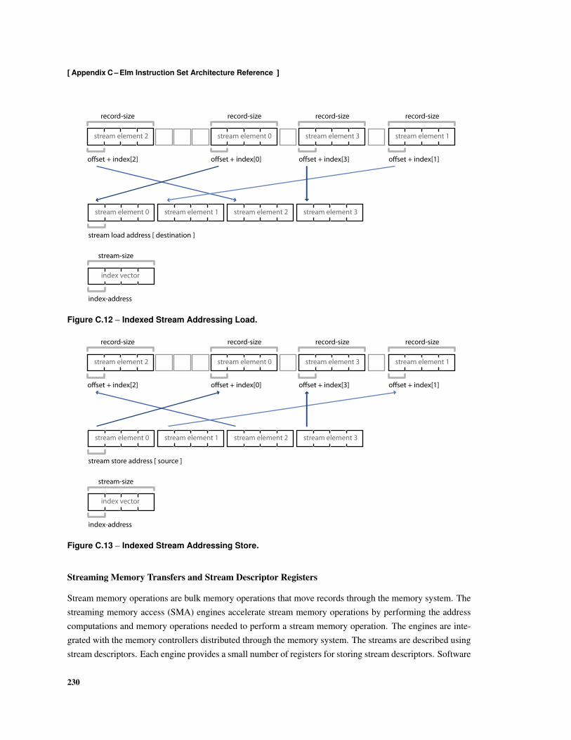
[ Appendix C – Elm Instruction Set Architecture Reference ]
record-size record-size
o!set + index[2] o!set + index[0]
stream element 2 stream element 0
stream element 0 stream element 1
record-size
o!set + index[3]
stream element 3
stream element 2
stream load address [ destination ]
index vector
index-address
stream-size
record-size
o!set + index[1]
stream element 1
stream element 3
Figure C.12 – Indexed Stream Addressing Load.
record-size record-size
o!set + index[2] o!set + index[0]
stream element 2 stream element 0
stream element 0 stream element 1
record-size
o!set + index[3]
stream element 3
stream element 2
stream store address [ source ]
index vector
index-address
stream-size
record-size
o!set + index[1]
stream element 1
stream element 3
Figure C.13 – Indexed Stream Addressing Store.
Streaming Memory Transfers and Stream Descriptor Registers
Stream memory operations are bulk memory operations that move records through the memory system. Thestreaming memory access (SMA) engines accelerate stream memory operations by performing the addresscomputations and memory operations needed to perform a stream memory operation. The engines are inte-grated with the memory controllers distributed through the memory system. The streams are described usingstream descriptors. Each engine provides a small number of registers for storing stream descriptors. Software
230

[ Supplimentary Section C.5 – Memory System ]
record-size:32 length:32 stride:32 index-address:32
Figure C.14 – Record Stream Descriptor.
opcode:8 rs3:6 rd:6 rs1:6 rs2:6
opcode:8 imm:6 rd:6 rs1:6 rs2:6
Figure C.15 – Instruction Format Used by Stream Operations.
registers a stream descriptor with an engine before initiating a stream memory operation.
Memory operations are performed over the on-chip network. The controllers exchange messages to com-plete memory operations. The following paragraphs describe the operations and the message formats. Eachoperation has a request and response message type. The request is used to initiate an operation, and theresponse to complete the operation or acknowledge that it completed.
Conceptually, streams are sequences of records. Stream memory operations move records through thememory hierarchy. Stream load operations collect and pack records into a contiguous range of memory, andstream store operations unpack and distribute records from a contiguous range of memory. Stream descriptorsare used to describe the layout of the records in memory: the descriptors provide succinct descriptions thatallow the hardware to determine where the records composing a stream reside in memory. The format of astream descriptor is shown in Figure C.14.
The processor dispatches streaming memory operations to streaming memory access (SMA) engines,which are distributed throughout the memory system, instead of executing them directly. The operations aredispatched as messages that are sent over the on-chip network. The SMA engines coordinate the sequencesof primitive memory operations (loads and stores) that are needed to complete a streaming memory opera-tion. Address generators within the SMA engines generate the sequences of memory addresses. Streamingmemory access engines are distributed throughout the memory system. To execute a streaming memory op-eration, a processor registers a stream descriptor with the SMA engine that will perform the operation andthen dispatches the streaming memory operation to the SMA engine. The stream descriptors are composedin memory and then transferred to stream descriptor registers in SMA engines. The instruction format usedby the stream memory operations is shown in Figure C.15.
Load Stream Descriptor [ ld.sd ]
This instruction transfers a stream descriptor from memory into a stream descriptor register in an SMAengine. The address argument provides the memory address, and the register address specifies the streamdescriptor register.
ld.sd <register> <address>
231

[ Appendix C – Elm Instruction Set Architecture Reference ]
register ← [ <rd> ]
addresss ← [ <rs1> + <rs2> ]
| [ <rs1> + <immediate:int6> ]
Store Stream Descriptor [ st.sd ]
This instruction transfers a stream descriptor from a stream descriptor register in an SMA engine to mem-ory. The address argument provides the memory address, and the register address specifies the streamdescriptor register.
st.sd <register> <address>
register ← [ <rd> ]
addresss ← [ <rs1> + <rs2> ]
| [ <rs1> + <immediate:int6> ]
Load Stream [ ld.stream ]
Loads stream elements to the address specified by dest. The remote addresses of the records are calculatedby adding the offset operand to the sequence of addresses generated by the stream descriptor named bystream. The number of records to be transferred is specified by the elements operand.
ld.stream <dest> [ <stream> + <offset> ] ( <elements> )
dest ← [ <rd> ]
stream ← [ <rs1> ]
offset ← <rs2>
elements ← <rs3>
| <immediate:int6>
Store Stream [ st.stream]
Stores stream elements from the address specified by source. The remote addresses of the records arecalculated by adding the offset operand to the sequence of addresses generated by the stream descriptornamed by by stream. The number of records to be transferred is specified by the elements operand.
st.stream <source> [ <stream> + <offset> ] ( <elements> )
source ← [ <rd> ]
stream ← [ <rs1> ]
offset ← <rs2>
elements ← <rs3>
| <immediate:int6>
232
[ Supplimentary Section C.5 – Memory System ]
Synchronize Stream Transfer [ sync.stream ]
Causes the processor to stall until a stream load or store completes. The operation is identified using thestream descriptor register, which is named by operand rs1.
sync.stream [ <rs1> ]
233

Bibliography
[1] D. Abts, S. Scott, and D.J. Lilja. So many states, so little time: Verifying memory coherence in the
Cray X1. In International Parallel and Distributed Processing Symposium (IPDPS), 2003.
[2] Yehuda Afek, Eytan Weisberger, and Hanan Weisman. A completeness theorem for a class of syn-
chronization objects. In PODC ’93: Proceedings of the twelfth annual ACM symposium on Principles
of distributed computing, pages 159–170, New York, NY, USA, 1993. ACM.
[3] A. Agarwal, D. Chaiken, K. Johnson, D. Kranz, J. Kubiatowicz, K. Kurihara, B. H. Lim, G. Maa,
D. Nussbaum, M. Parkin, and D. Yeung. The MIT alewife machine: A large-scale distributed memory
multiprocessor. Technical report, Massachusetts Institute of Technology, Cambridge, MA, USA, 1991.
[4] Anant Agarwal, Ricardo Bianchini, David Chaiken, Kirk L. Johnson, David Kranz, John Kubiatowicz,
Beng-Hong Lim, Kenneth Mackenzie, and Donald Yeung. The mit alewife machine: architecture and
performance. In ISCA ’95: Proceedings of the 22nd annual international symposium on Computer
architecture, pages 2–13, New York, NY, USA, 1995. ACM.
[5] Anant Agarwal and Markus Levy. The kill rule for multicore. In DAC ’07: Proceedings of the 44th
annual Design Automation Conference, pages 750–753, New York, NY, USA, 2007. ACM.
[6] T. Agerwala and J. Cocke. High Performance Reduced Instruction Set Processors. IBM Thomas J.
Watson Research Center Technical Report, 558845, 1987.
[7] N. Ahmed, T. Natarajan, and K. R. Rao. Discrete cosine transfom. IEEE Transactions on Computing,
23(1):90–93, 1974.
[8] A. Allen, J. Desai, F. Verdico, F. Anderson, D. Mulvihill, and D. Krueger. Dynamic frequency-
switching clock system on a quad-core itanium processor. In Solid-State Circuits Conference - Digest
of Technical Papers, 2009. ISSCC 2009. IEEE International, pages 62 –63,63a, Feb. 2009.
[9] Arvind and Vinod Kathail. A multiple processor data flow machine that supports generalized pro-
cedures. In ISCA ’81: Proceedings of the 8th annual symposium on Computer Architecture, pages
291–302, Los Alamitos, CA, USA, 1981. IEEE Computer Society Press.
234
[ BIBLIOGRAPHY ]
[10] Krste Asanovic. Vector Microprocessors. PhD dissertation, University of California at Berkeley,
Berkeley, CA, USA, 1998.
[11] Krste Asanovic, Ras Bodik, Bryan Christopher Catanzaro, Joseph James Gebis, Parry Husbands, Kurt
Keutzer, David A. Patterson, William Lester Plishker, John Shalf, Samuel Webb Williams, and Kather-
ine A. Yelick. The landscape of parallel computing research: A view from berkeley. Technical Report
UCB/EECS-2006-183, EECS Department, University of California, Berkeley, Dec 2006.
[12] James Balfour, William J. Dally, David Black-Schaffer, Vishal Parikh, and Jongsoo Park. An energy-
efficient processor architecture for embedded systems. Computer Architecture Letters, pages 29–32,
2008.
[13] James Balfour, R. Curtis Harting, and William J. Dally. Operand registers and explicit operand for-
warding. Computer Architecture Letters, 2009.
[14] Max Baron. Silicon à la carte. Microprocessor Report, January 2004.
[15] Luiz André Barroso, Kourosh Gharachorloo, Robert McNamara, Andreas Nowatzyk, Shaz Qadeer,
Barton Sano, Scott Smith, Robert Stets, and Ben Verghese. Piranha: a scalable architecture based on
single-chip multiprocessing. In ISCA ’00: Proceedings of the 27th annual international symposium
on Computer architecture, pages 282–293, New York, NY, USA, 2000. ACM.
[16] K. E. Batcher. Sorting networks and their applications. In AFIPS ’68 (Spring): Proceedings of the
April 30–May 2, 1968, spring joint computer conference, pages 307–314, New York, NY, USA, 1968.
ACM.
[17] Christopher Batten, Ronny Krashinsky, Steve Gerding, and Krste Asanovic. Cache refill/access decou-
pling for vector machines. In MICRO 37: Proceedings of the 37th annual IEEE/ACM International
Symposium on Microarchitecture, pages 331–342, Washington, DC, USA, 2004. IEEE Computer So-
ciety.
[18] S. Bell, B. Edwards, J. Amann, R. Conlin, K. Joyce, V. Leung, J. MacKay, M. Reif, J. Liewei Bao,
Brown, M. Mattina, C. Chyi-Chang Miao, Ramey, D. Wentzlaff, W. Anderson, E. Berger, N. Fairbanks,
D. Khan, F. Montenegro, J. Stickney, and J. and Zook. TILE64 – Processor: A 64-Core SoC with Mesh
Interconnect. pages 88 –598, Feb. 2008.
[19] David Black-Schaffer, James Balfour, William J. Dally, Vishal Parikh, and Jongsoo Park. Hierarchical
instruction register organizations. Computer Architecture Letters, 2008.
[20] D. Callahan, K. Kennedy, and A. Porterfield. Software Prefetching. ACM SIGARCH Computer Archi-
tecture News, 19(2):52, 1991.
[21] Anantha P. Chandrakasan, Samuel Sheng, and Robert W. Brodersen. Low Power CMOS Digital De-
sign. IEEE Journal of Solid State Circuits, 27:473–484, 1995.
235

[ BIBLIOGRAPHY ]
[22] L. Chang, D.J. Frank, R.K. Montoye, S.J. Koester, B.L. Ji, P.W. Coteus, R.H. Dennard, and W. Haen-
sch. Practical strategies for power-efficient computing technologies. Proceedings of the IEEE,
98(2):215 –236, feb. 2010.
[23] Nathan Clark, Jason Blome, Michael Chu, Scott Mahlke, Stuart Biles, and Krisztian Flautner. An
architecture framework for transparent instruction set customization in embedded processors. In ISCA
’05: Proceedings of the 32nd annual international symposium on Computer Architecture, pages 272–
283, Washington, DC, USA, 2005. IEEE Computer Society.
[24] Robert P. Colwell, W. Eric Hall, Chandra S. Joshi, David B. Papworth, Paul K. Rodman, and James E.
Tornes. Architecture and implementation of a VLIW supercomputer. In Supercomputing ’90: Pro-
ceedings of the 1990 ACM/IEEE conference on Supercomputing, pages 910–919, Los Alamitos, CA,
USA, 1990. IEEE Computer Society Press.
[25] D. Coppersmith. The Data Encryption Standard (DES) and its strength against attacks. IBM Journal
of Research and Development, 38(3):243–250, 1994.
[26] IBM Corporation. PowerPC Microprocessor Family: The Programming Environments for 32-Bit Mi-
croprocessors. IBM Corporation, February 2000.
[27] IBM Corporation. PowerPC Microprocessor Family: Vector/SIMD Multimedia Extension Technology
Programming Environments Manual. IBM Corporation, August 2005.
[28] Intel Corporation. Intel Itanium Architecture Software Developer’s Manual. Intel Corporation, January
2006.
[29] Cray Research, Inc. CRAY-1 Hardware Reference Manual, Rev. C. Cray Resarch, Inc., 1977.
[30] José-Lorenzo Cruz, Antonio González, Mateo Valero, and Nigel P. Topham. Multiple-banked register
file architectures. In ISCA ’00: Proceedings of the 27th Annual International Symposium on Computer
Architecture, pages 316–325, 2000.
[31] J. Daemen and V. Rijmen. The design of Rijndael. Springer-Verlag New York, Inc. Secaucus, NJ,
USA, 2002.
[32] W. J. Dally, L. Chao, A. Chien, S. Hassoun, W. Horwat, J. Kaplan, P. Song, B. Totty, and S. Wills.
Architecture of a message-driven processor. In ISCA ’87: Proceedings of the 14th annual international
symposium on Computer architecture, pages 189–196, New York, NY, USA, 1987. ACM.
[33] William J. Dally, James Balfour, David Black-Schaffer, James Chen, R. Curtis Harting, Vishal Parikh,
Jongsoo Park, and David Sheffield. Efficient embedded computing. IEEE Computer, July 2008.
236

[ BIBLIOGRAPHY ]
[34] William J. Dally, J. A. Stuart Fiske, John S. Keen, Richard A. Lethin, Michael D. Noakes, Peter R.
Nuth, Roy E. Davison, and Gregory A. Fyler. The message-driven processor: A multicomputer pro-
cessing node with efficient mechanisms. IEEE Micro, 12(2):23–39, 1992.
[35] William J. Dally, Ujval J. Kapasi, Brucek Khailany, Jung Ho Ahn, and Abhishek Das. Stream proces-
sors: Progammability and efficiency. Queue, 2(1):52–62, 2004.
[36] Robert H. Dennard, Fritz H. Gaensslen, Hwa-Nien Yu, V. Leo Rideout, Ernest Bassous, and Andre R.
Leblanc. Design of ion-implanted MOSFET’s with very small physical dimensions. IEEE Journal of
Solid-State Circuits, pages 256–268, October 1974.
[37] Jeff H. Derby, Robert K. Montoye, and José Moreira. VICTORIA: VMX indirect compute technology
oriented towards in-line acceleration. In CF ’06: Proceedings of the 3rd conference on Computing
frontiers, pages 303–312, New York, NY, USA, 2006. ACM.
[38] Roger Espasa, Federico Ardanaz, Joel Emer, Stephen Felix, Julio Gago, Roger Gramunt, Isaac Her-
nandez, Toni Juan, Geoff Lowney, Matthew Mattina, and André Seznec. Tarantula: a vector extension
to the alpha architecture. SIGARCH Comput. Archit. News, 30(2):281–292, 2002.
[39] Greg Faanes. A CMOS Vector Processor with a Custom Streaming Cache. In Proceedings of Hot
Chips, volume 10, 1998.
[40] Keith I. Farkas, Paul Chow, Norman P. Jouppi, and Zvonko Vranesic. The multicluster architecture:
Reducing processor cycle time through partitioning. International Journal of Parallel Programming,
27(5):327–356, 1999.
[41] Kayvon Fatahalian and Mike Houston. A closer look at GPUs. Commununications of the ACM,
51(10):50–57, 2008.
[42] Joseph A. Fisher. Very long instruction word architectures and the eli-512. In ISCA ’83: Proceedings
of the 10th annual international symposium on Computer architecture, pages 140–150, New York, NY,
USA, 1983. ACM.
[43] Josh A. Fisher, Paolo Faraboschi, and Cliff Young. Embedded Computing: A VLIW approach to
Architecture, Compilers and Tools. Morgan Kaufmann Publishing, 2005.
[44] Mark Gebhart, Bertrand A. Maher, Katherine E. Coons, Jeff Diamond, Paul Gratz, Mario Marino,
Nitya Ranganathan, Behnam Robatmili, Aaron Smith, James Burrill, Stephen W. Keckler, Doug
Burger, and Kathryn S. McKinley. An evaluation of the trips computer system. In ASPLOS ’09:
Proceeding of the 14th international conference on Architectural support for programming languages
and operating systems, pages 1–12, New York, NY, USA, 2009. ACM.
237
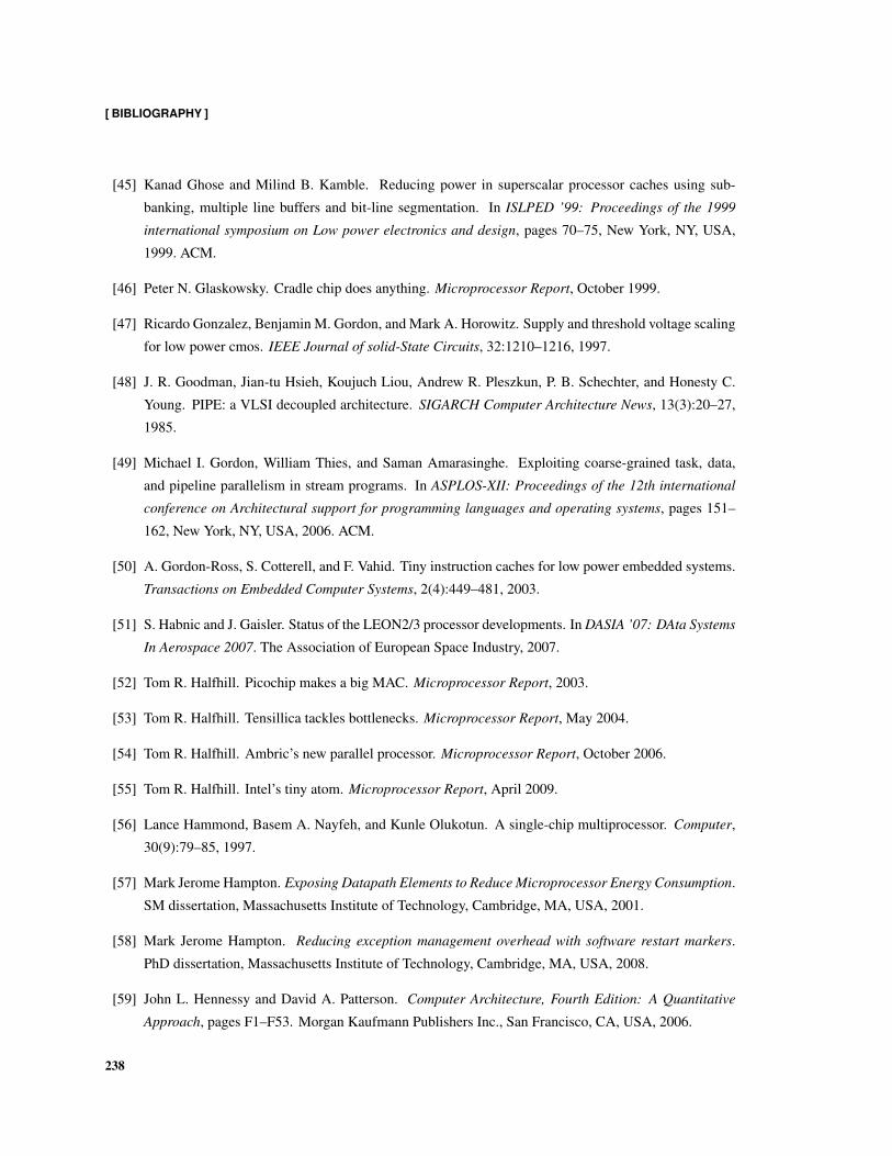
[ BIBLIOGRAPHY ]
[45] Kanad Ghose and Milind B. Kamble. Reducing power in superscalar processor caches using sub-
banking, multiple line buffers and bit-line segmentation. In ISLPED ’99: Proceedings of the 1999
international symposium on Low power electronics and design, pages 70–75, New York, NY, USA,
1999. ACM.
[46] Peter N. Glaskowsky. Cradle chip does anything. Microprocessor Report, October 1999.
[47] Ricardo Gonzalez, Benjamin M. Gordon, and Mark A. Horowitz. Supply and threshold voltage scaling
for low power cmos. IEEE Journal of solid-State Circuits, 32:1210–1216, 1997.
[48] J. R. Goodman, Jian-tu Hsieh, Koujuch Liou, Andrew R. Pleszkun, P. B. Schechter, and Honesty C.
Young. PIPE: a VLSI decoupled architecture. SIGARCH Computer Architecture News, 13(3):20–27,
1985.
[49] Michael I. Gordon, William Thies, and Saman Amarasinghe. Exploiting coarse-grained task, data,
and pipeline parallelism in stream programs. In ASPLOS-XII: Proceedings of the 12th international
conference on Architectural support for programming languages and operating systems, pages 151–
162, New York, NY, USA, 2006. ACM.
[50] A. Gordon-Ross, S. Cotterell, and F. Vahid. Tiny instruction caches for low power embedded systems.
Transactions on Embedded Computer Systems, 2(4):449–481, 2003.
[51] S. Habnic and J. Gaisler. Status of the LEON2/3 processor developments. In DASIA ’07: DAta Systems
In Aerospace 2007. The Association of European Space Industry, 2007.
[52] Tom R. Halfhill. Picochip makes a big MAC. Microprocessor Report, 2003.
[53] Tom R. Halfhill. Tensillica tackles bottlenecks. Microprocessor Report, May 2004.
[54] Tom R. Halfhill. Ambric’s new parallel processor. Microprocessor Report, October 2006.
[55] Tom R. Halfhill. Intel’s tiny atom. Microprocessor Report, April 2009.
[56] Lance Hammond, Basem A. Nayfeh, and Kunle Olukotun. A single-chip multiprocessor. Computer,
30(9):79–85, 1997.
[57] Mark Jerome Hampton. Exposing Datapath Elements to Reduce Microprocessor Energy Consumption.
SM dissertation, Massachusetts Institute of Technology, Cambridge, MA, USA, 2001.
[58] Mark Jerome Hampton. Reducing exception management overhead with software restart markers.
PhD dissertation, Massachusetts Institute of Technology, Cambridge, MA, USA, 2008.
[59] John L. Hennessy and David A. Patterson. Computer Architecture, Fourth Edition: A Quantitative
Approach, pages F1–F53. Morgan Kaufmann Publishers Inc., San Francisco, CA, USA, 2006.
238
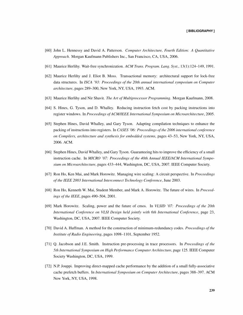
[ BIBLIOGRAPHY ]
[60] John L. Hennessy and David A. Patterson. Computer Architecture, Fourth Edition: A Quantitative
Approach. Morgan Kaufmann Publishers Inc., San Francisco, CA, USA, 2006.
[61] Maurice Herlihy. Wait-free synchronization. ACM Trans. Program. Lang. Syst., 13(1):124–149, 1991.
[62] Maurice Herlihy and J. Eliot B. Moss. Transactional memory: architectural support for lock-free
data structures. In ISCA ’93: Proceedings of the 20th annual international symposium on Computer
architecture, pages 289–300, New York, NY, USA, 1993. ACM.
[63] Maurice Herlihy and Nir Shavit. The Art of Multiprocessor Programming. Morgan Kaufmann, 2008.
[64] S. Hines, G. Tyson, and D. Whalley. Reducing instruction fetch cost by packing instructions into
register windows. In Proceedings of ACM/IEEE International Symposium on Microarchitecture, 2005.
[65] Stephen Hines, David Whalley, and Gary Tyson. Adapting compilation techniques to enhance the
packing of instructions into registers. In CASES ’06: Proceedings of the 2006 international conference
on Compilers, architecture and synthesis for embedded systems, pages 43–53, New York, NY, USA,
2006. ACM.
[66] Stephen Hines, David Whalley, and Gary Tyson. Guaranteeing hits to improve the efficiency of a small
instruction cache. In MICRO ’07: Proceedings of the 40th Annual IEEE/ACM International Sympo-
sium on Microarchitecture, pages 433–444, Washington, DC, USA, 2007. IEEE Computer Society.
[67] Ron Ho, Ken Mai, and Mark Horowitz. Managing wire scaling: A circuit perspective. In Proceedings
of the IEEE 2003 International Interconnect Technology Conference, June 2003.
[68] Ron Ho, Kenneth W. Mai, Student Member, and Mark A. Horowitz. The future of wires. In Proceed-
ings of the IEEE, pages 490–504, 2001.
[69] Mark Horowitz. Scaling, power and the future of cmos. In VLSID ’07: Proceedings of the 20th
International Conference on VLSI Design held jointly with 6th International Conference, page 23,
Washington, DC, USA, 2007. IEEE Computer Society.
[70] David A. Huffman. A method for the construction of minimum-redundancy codes. Proceedings of the
Institute of Radio Engineering, pages 1098–1101, September 1952.
[71] Q. Jacobson and J.E. Smith. Instruction pre-processing in trace processors. In Proceedings of the
5th International Symposium on High Performance Computer Architecture, page 125. IEEE Computer
Society Washington, DC, USA, 1999.
[72] N.P. Jouppi. Improving direct-mapped cache performance by the addition of a small fully-associative
cache prefetch buffers. In International Symposium on Computer Architecture, pages 388–397. ACM
New York, NY, USA, 1998.
239
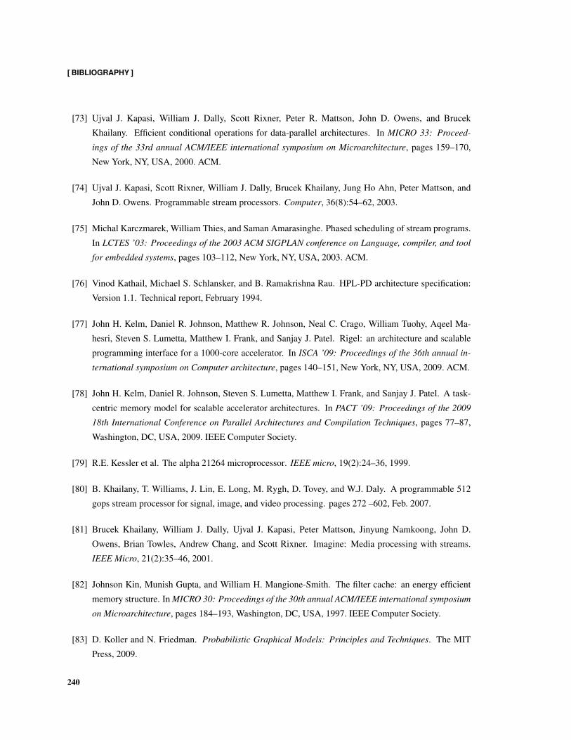
[ BIBLIOGRAPHY ]
[73] Ujval J. Kapasi, William J. Dally, Scott Rixner, Peter R. Mattson, John D. Owens, and Brucek
Khailany. Efficient conditional operations for data-parallel architectures. In MICRO 33: Proceed-
ings of the 33rd annual ACM/IEEE international symposium on Microarchitecture, pages 159–170,
New York, NY, USA, 2000. ACM.
[74] Ujval J. Kapasi, Scott Rixner, William J. Dally, Brucek Khailany, Jung Ho Ahn, Peter Mattson, and
John D. Owens. Programmable stream processors. Computer, 36(8):54–62, 2003.
[75] Michal Karczmarek, William Thies, and Saman Amarasinghe. Phased scheduling of stream programs.
In LCTES ’03: Proceedings of the 2003 ACM SIGPLAN conference on Language, compiler, and tool
for embedded systems, pages 103–112, New York, NY, USA, 2003. ACM.
[76] Vinod Kathail, Michael S. Schlansker, and B. Ramakrishna Rau. HPL-PD architecture specification:
Version 1.1. Technical report, February 1994.
[77] John H. Kelm, Daniel R. Johnson, Matthew R. Johnson, Neal C. Crago, William Tuohy, Aqeel Ma-
hesri, Steven S. Lumetta, Matthew I. Frank, and Sanjay J. Patel. Rigel: an architecture and scalable
programming interface for a 1000-core accelerator. In ISCA ’09: Proceedings of the 36th annual in-
ternational symposium on Computer architecture, pages 140–151, New York, NY, USA, 2009. ACM.
[78] John H. Kelm, Daniel R. Johnson, Steven S. Lumetta, Matthew I. Frank, and Sanjay J. Patel. A task-
centric memory model for scalable accelerator architectures. In PACT ’09: Proceedings of the 2009
18th International Conference on Parallel Architectures and Compilation Techniques, pages 77–87,
Washington, DC, USA, 2009. IEEE Computer Society.
[79] R.E. Kessler et al. The alpha 21264 microprocessor. IEEE micro, 19(2):24–36, 1999.
[80] B. Khailany, T. Williams, J. Lin, E. Long, M. Rygh, D. Tovey, and W.J. Daly. A programmable 512
gops stream processor for signal, image, and video processing. pages 272 –602, Feb. 2007.
[81] Brucek Khailany, William J. Dally, Ujval J. Kapasi, Peter Mattson, Jinyung Namkoong, John D.
Owens, Brian Towles, Andrew Chang, and Scott Rixner. Imagine: Media processing with streams.
IEEE Micro, 21(2):35–46, 2001.
[82] Johnson Kin, Munish Gupta, and William H. Mangione-Smith. The filter cache: an energy efficient
memory structure. In MICRO 30: Proceedings of the 30th annual ACM/IEEE international symposium
on Microarchitecture, pages 184–193, Washington, DC, USA, 1997. IEEE Computer Society.
[83] D. Koller and N. Friedman. Probabilistic Graphical Models: Principles and Techniques. The MIT
Press, 2009.
240
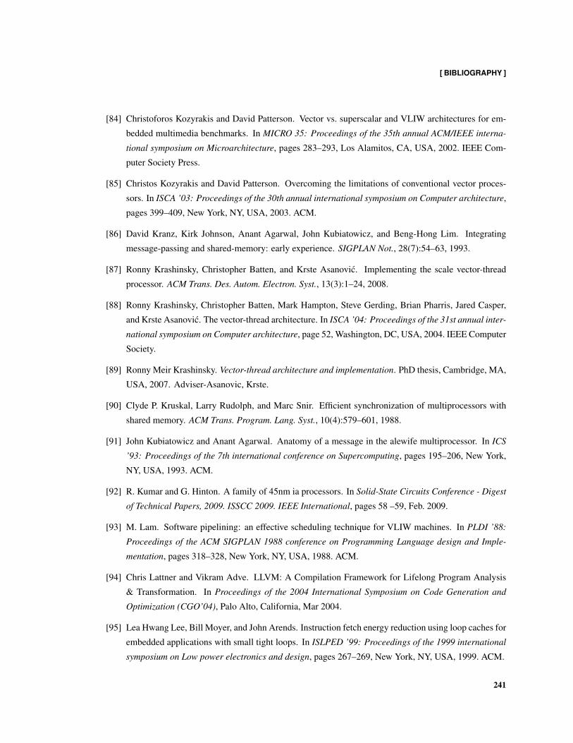
[ BIBLIOGRAPHY ]
[84] Christoforos Kozyrakis and David Patterson. Vector vs. superscalar and VLIW architectures for em-
bedded multimedia benchmarks. In MICRO 35: Proceedings of the 35th annual ACM/IEEE interna-
tional symposium on Microarchitecture, pages 283–293, Los Alamitos, CA, USA, 2002. IEEE Com-
puter Society Press.
[85] Christos Kozyrakis and David Patterson. Overcoming the limitations of conventional vector proces-
sors. In ISCA ’03: Proceedings of the 30th annual international symposium on Computer architecture,
pages 399–409, New York, NY, USA, 2003. ACM.
[86] David Kranz, Kirk Johnson, Anant Agarwal, John Kubiatowicz, and Beng-Hong Lim. Integrating
message-passing and shared-memory: early experience. SIGPLAN Not., 28(7):54–63, 1993.
[87] Ronny Krashinsky, Christopher Batten, and Krste Asanovic. Implementing the scale vector-thread
processor. ACM Trans. Des. Autom. Electron. Syst., 13(3):1–24, 2008.
[88] Ronny Krashinsky, Christopher Batten, Mark Hampton, Steve Gerding, Brian Pharris, Jared Casper,
and Krste Asanovic. The vector-thread architecture. In ISCA ’04: Proceedings of the 31st annual inter-
national symposium on Computer architecture, page 52, Washington, DC, USA, 2004. IEEE Computer
Society.
[89] Ronny Meir Krashinsky. Vector-thread architecture and implementation. PhD thesis, Cambridge, MA,
USA, 2007. Adviser-Asanovic, Krste.
[90] Clyde P. Kruskal, Larry Rudolph, and Marc Snir. Efficient synchronization of multiprocessors with
shared memory. ACM Trans. Program. Lang. Syst., 10(4):579–601, 1988.
[91] John Kubiatowicz and Anant Agarwal. Anatomy of a message in the alewife multiprocessor. In ICS
’93: Proceedings of the 7th international conference on Supercomputing, pages 195–206, New York,
NY, USA, 1993. ACM.
[92] R. Kumar and G. Hinton. A family of 45nm ia processors. In Solid-State Circuits Conference - Digest
of Technical Papers, 2009. ISSCC 2009. IEEE International, pages 58 –59, Feb. 2009.
[93] M. Lam. Software pipelining: an effective scheduling technique for VLIW machines. In PLDI ’88:
Proceedings of the ACM SIGPLAN 1988 conference on Programming Language design and Imple-
mentation, pages 318–328, New York, NY, USA, 1988. ACM.
[94] Chris Lattner and Vikram Adve. LLVM: A Compilation Framework for Lifelong Program Analysis
& Transformation. In Proceedings of the 2004 International Symposium on Code Generation and
Optimization (CGO’04), Palo Alto, California, Mar 2004.
[95] Lea Hwang Lee, Bill Moyer, and John Arends. Instruction fetch energy reduction using loop caches for
embedded applications with small tight loops. In ISLPED ’99: Proceedings of the 1999 international
symposium on Low power electronics and design, pages 267–269, New York, NY, USA, 1999. ACM.
241

[ BIBLIOGRAPHY ]
[96] Walter Lee, Rajeev Barua, Matthew Frank, Devabhaktuni Srikrishna, Jonathan Babb, Vivek Sarkar,
and Saman Amarasinghe. Space-time scheduling of instruction-level parallelism on a raw machine.
SIGPLAN Not., 33(11):46–57, 1998.
[97] A.S. Leon, J.L. Shin, K.W. Tam, W. Bryg, F. Schumacher, P. Kongetira, D. Weisner, and A. Strong. A
power-efficient high-throughput 32-thread sparc processor. pages 295 – 304, Feb. 2006.
[98] Yuan Lin, Hyunseok Lee, Mark Woh, Yoav Harel, Scott Mahlke, Trevor Mudge, Chaitali Chakrabarti,
and Krisztian Flautner. SODA: A low-power architecture for software radio. In ISCA ’06: Proceedings
of the 33rd annual international symposium on Computer Architecture, pages 89–101, Washington,
DC, USA, 2006. IEEE Computer Society.
[99] Erik Lindholm, John Nickolls, Stuart Oberman, and John Montrym. Nvidia tesla: A unified graphics
and computing architecture. IEEE Micro, 28(2):39–55, 2008.
[100] John D. C. Little. A proof of the queuing formula: L = λW . Operations Research, 9(3):383–387,
1961.
[101] D. Marr and E. Hildreth. Theory of edge detection. Proceedings of the Royal Society of London. Series
B, Biological Sciences, pages 187–217, 1980.
[102] Yves Mathys and André Châtelain. Verification strategy for integration 3G baseband SoC. In DAC
’03: Proceedings of the 40th conference on Design automation, pages 7–10, New York, NY, USA,
2003. ACM Press.
[103] Stephen Melvin and Yale Patt. Enhancing instruction scheduling with a block-structured ISA. Inter-
national Journal of Parallel Programming, 23(3):221–243, 1995.
[104] Sun Microsystems. UtraSPARC Architecture 2007. Sun Microsystems, draft D0.9.3b edition, October
2009.
[105] J. Montanaro, R.T. Witek, K. Anne, A.J. Black, E.M. Cooper, D.W. Dobberpuhl, P.M. Donahue,
J. Eno, W. Hoeppner, D. Kruckemyer, T.H. Lee, P.C.M. Lin, L. Madden, D. Murray, M.H. Pearce,
S. Santhanam, K.J. Snyder, R. Stehpany, and S.C. Thierauf. A 160-MHz, 32-b, 0.5-w CMOS RISC
microprocessor. Solid-State Circuits, IEEE Journal of, 31(11):1703–1714, Nov 1996.
[106] J. H. Moreno, V. Zyuban, U. Shvadron, F. D. Neeser, J. H. Derby, M. S. Ware, K. Kailas, A. Zaks,
A. Geva, S. Ben-David, S. W. Asaad, T. W. Fox, D. Littrell, M. Biberstein, D. Naishlos, and H. Hunter.
An innovative low-power high-performance programmable signal processor for digital communica-
tions. IBM Journal of Reseasrch and Development, 47(2-3):299–326, 2003.
242

[ BIBLIOGRAPHY ]
[107] Ramadass Nagarajan, Karthikeyan Sankaralingam, Doug Burger, and Stephen W. Keckler. A de-
sign space evaluation of grid processor architectures. In MICRO 34: Proceedings of the 34th an-
nual ACM/IEEE international symposium on Microarchitecture, pages 40–51, Washington, DC, USA,
2001. IEEE Computer Society.
[108] U.G. Nawathe, M. Hassan, K.C. Yen, A. Kumar, A. Ramachandran, and D. Greenhill. Implementation
of an 8-core, 64-thread, power-efficient sparc server on a chip. Solid-State Circuits, IEEE Journal of,
43(1):6 –20, Jan. 2008.
[109] J. Nechvatal, E. Barker, L. Bassham, W. Burr, M. Dworkin, J. Foti, and E. Roback. Report on the
development of the Advanced Encryption Standard (AES). JOURNAL OF RESEARCH-NATIONAL
INSTITUTE OF STANDARDS AND TECHNOLOGY, 106(3):511–576, 2001.
[110] Richard van Nee and Ramjee Prasad. OFDM for Wireless Multimedia Communications. Artech House,
Inc., Norwood, MA, USA, 2000.
[111] Chris J. Newburn, Andrew S. Huang, and John Paul Shen. Balancing fine- and medium-grained paral-
lelism in scheduling loops for the ximd architecture. In PACT ’93: Proceedings of the IFIP WG10.3.
Working Conference on Architectures and Compilation Techniques for Fine and Medium Grain Paral-
lelism, pages 39–52, Amsterdam, The Netherlands, The Netherlands, 1993. North-Holland Publishing
Co.
[112] Kunle Olukotun, Basem A. Nayfeh, Lance Hammond, Ken Wilson, and Kunyung Chang. The case for
a single-chip multiprocessor. SIGPLAN Not., 31(9):2–11, 1996.
[113] Gregory M. Papadopoulos and David E. Culler. Monsoon: an explicit token-store architecture. In
ISCA ’90: Proceedings of the 17th annual international symposium on Computer Architecture, pages
82–91, New York, NY, USA, 1990. ACM.
[114] David A. Patterson and Carlo H. Sequin. Risc i: A reduced instruction set vlsi computer. In ISCA ’81:
Proceedings of the 8th annual symposium on Computer Architecture, pages 443–457, Los Alamitos,
CA, USA, 1981. IEEE Computer Society Press.
[115] M.J.M. Pelgrom, A.C.J. Duinmaijer, A.P.G. Welbers, et al. Matching properties of MOS transistors.
IEEE journal of solid-state circuits, 24(5):1433–1439, 1989.
[116] Miquel Pericàs, Eduard Ayguadé, Javier Zalamea, Josep Llosa, and Mateo Valero. Power-efficient
VLIW design using clustering and widening. International Journal of Embedded Systems, 3(3):141–
149, 2008.
[117] L. Pileggi, G. Keskin, X. Li, K. Mai, and J. Proesel. Mismatch analysis and statistical design at 65 nm
and below. In IEEE Custom Integrated Circuits Conference, 2008.
243
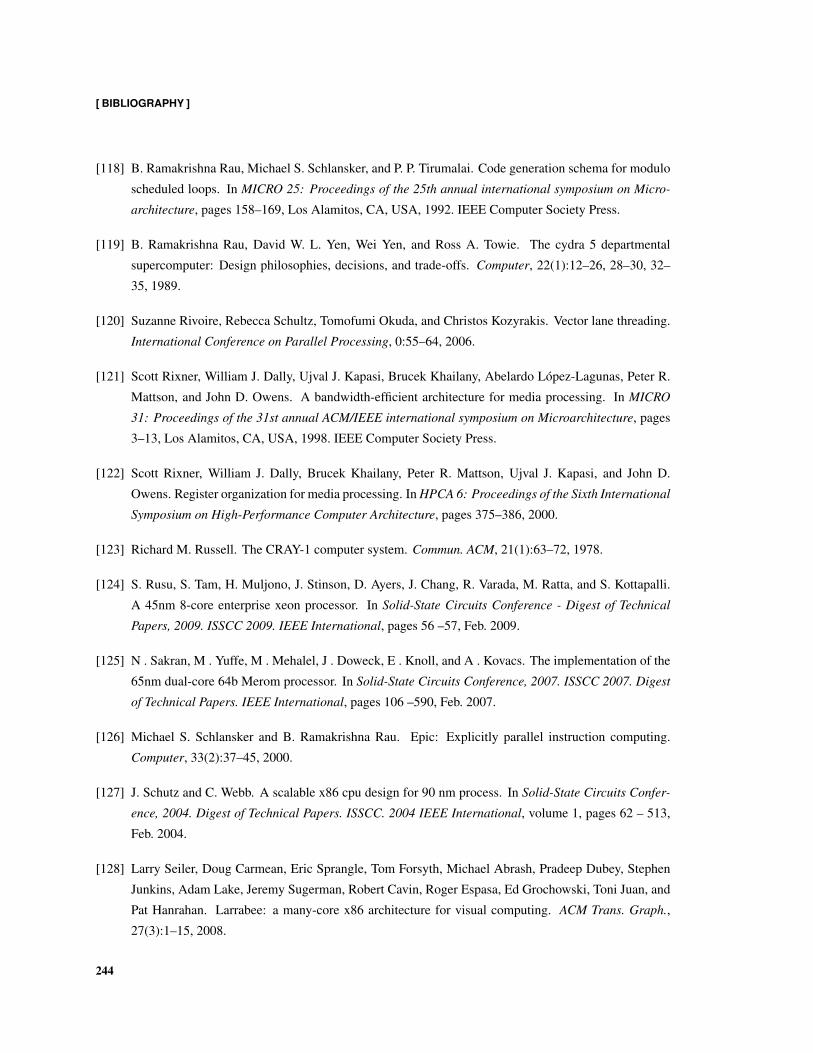
[ BIBLIOGRAPHY ]
[118] B. Ramakrishna Rau, Michael S. Schlansker, and P. P. Tirumalai. Code generation schema for modulo
scheduled loops. In MICRO 25: Proceedings of the 25th annual international symposium on Micro-
architecture, pages 158–169, Los Alamitos, CA, USA, 1992. IEEE Computer Society Press.
[119] B. Ramakrishna Rau, David W. L. Yen, Wei Yen, and Ross A. Towie. The cydra 5 departmental
supercomputer: Design philosophies, decisions, and trade-offs. Computer, 22(1):12–26, 28–30, 32–
35, 1989.
[120] Suzanne Rivoire, Rebecca Schultz, Tomofumi Okuda, and Christos Kozyrakis. Vector lane threading.
International Conference on Parallel Processing, 0:55–64, 2006.
[121] Scott Rixner, William J. Dally, Ujval J. Kapasi, Brucek Khailany, Abelardo López-Lagunas, Peter R.
Mattson, and John D. Owens. A bandwidth-efficient architecture for media processing. In MICRO
31: Proceedings of the 31st annual ACM/IEEE international symposium on Microarchitecture, pages
3–13, Los Alamitos, CA, USA, 1998. IEEE Computer Society Press.
[122] Scott Rixner, William J. Dally, Brucek Khailany, Peter R. Mattson, Ujval J. Kapasi, and John D.
Owens. Register organization for media processing. In HPCA 6: Proceedings of the Sixth International
Symposium on High-Performance Computer Architecture, pages 375–386, 2000.
[123] Richard M. Russell. The CRAY-1 computer system. Commun. ACM, 21(1):63–72, 1978.
[124] S. Rusu, S. Tam, H. Muljono, J. Stinson, D. Ayers, J. Chang, R. Varada, M. Ratta, and S. Kottapalli.
A 45nm 8-core enterprise xeon processor. In Solid-State Circuits Conference - Digest of Technical
Papers, 2009. ISSCC 2009. IEEE International, pages 56 –57, Feb. 2009.
[125] N . Sakran, M . Yuffe, M . Mehalel, J . Doweck, E . Knoll, and A . Kovacs. The implementation of the
65nm dual-core 64b Merom processor. In Solid-State Circuits Conference, 2007. ISSCC 2007. Digest
of Technical Papers. IEEE International, pages 106 –590, Feb. 2007.
[126] Michael S. Schlansker and B. Ramakrishna Rau. Epic: Explicitly parallel instruction computing.
Computer, 33(2):37–45, 2000.
[127] J. Schutz and C. Webb. A scalable x86 cpu design for 90 nm process. In Solid-State Circuits Confer-
ence, 2004. Digest of Technical Papers. ISSCC. 2004 IEEE International, volume 1, pages 62 – 513,
Feb. 2004.
[128] Larry Seiler, Doug Carmean, Eric Sprangle, Tom Forsyth, Michael Abrash, Pradeep Dubey, Stephen
Junkins, Adam Lake, Jeremy Sugerman, Robert Cavin, Roger Espasa, Ed Grochowski, Toni Juan, and
Pat Hanrahan. Larrabee: a many-core x86 architecture for visual computing. ACM Trans. Graph.,
27(3):1–15, 2008.
244

[ BIBLIOGRAPHY ]
[129] S. Seneff. System to independently modify excitation and/or spectrum of speech waveform without
explicit pitch extraction. IEEE Transactions on Acoustics, Speech and Signal Processing, 30(4):566 –
578, aug 1982.
[130] C. W. Sherwin, J. P. Ruina, and R. D. Rawcliffe. Some early developments in synthetic aperture radar
systems. Military Electronics, IRE Transactions on, MIL-6(2):111 –115, april 1962.
[131] Olli Silven and Kari Jyrkkä. Observations on power-efficiency trends in mobile communication de-
vices. EURASIP Journal of Embedded Systems, 2007(1):17–17, 2007.
[132] Mikhail Smelyanskiy, Gary S. Tyson, and Edward S. Davidson. Register queues: A new hardware/soft-
ware approach to efficient software pipelining. In PACT ’00: Proceedings of the 2000 International
Conference on Parallel Architectures and Compilation Techniques, page 3, Washington, DC, USA,
2000. IEEE Computer Society.
[133] A.J. Smith. Cache memories. ACM Computing Surveys (CSUR), 14(3):473–530, 1982.
[134] Burton J. Smith. Architecture and applications of the HEP multiprocessor computer system. In SPIE
Vol. 298 Real-Time Signal Processing IV, pages 241–248. Denelcor, Inc., 1981.
[135] J. E. Smith, Greg Faanes, and Rabin Sugumar. Vector instruction set support for conditional operations.
In ISCA ’00: Proceedings of the 27th annual international symposium on Computer architecture, pages
260–269, New York, NY, USA, 2000. ACM.
[136] Alex Solomatnikov, Amin Firoozshahian, Wajahat Qadeer, Ofer Shacham, Kyle Kelley, Zain Asgar,
Megan Wachs, Rehan Hameed, and Mark Horowitz. Chip multi-processor generator. In DAC ’07:
Proceedings of the 44th annual Design Automation Conference, pages 262–263, New York, NY, USA„
2007. ACM.
[137] Michael Bedford Taylor, Jason Kim, Jason Miller, David Wentzlaff, Fae Ghodrat, Ben Greenwald,
Henry Hoffman, Paul Johnson, Jae-Wook Lee, Walter Lee, Albert Ma, Arvind Saraf, Mark Seneski,
Nathan Shnidman, Volker Strumpen, Matt Frank, Saman Amarasinghe, and Anant Agarwal. The raw
microprocessor: A computational fabric for software circuits and general-purpose programs. IEEE
Micro, 22(2):25–35, 2002.
[138] Michael Bedford Taylor, Walter Lee, Saman Amarasinghe, and Anant Agarwal. Scalar operand net-
works: On-chip interconnect for ilp in partitioned architectures. In HPCA ’03: Proceedings of the 9th
International Symposium on High-Performance Computer Architecture, page 341, Washington, DC,
USA, 2003. IEEE Computer Society.
[139] Michael Bedford Taylor, Walter Lee, Jason Miller, David Wentzlaff, Ian Bratt, Ben Greenwald, Henry
Hoffmann, Paul Johnson, Jason Kim, James Psota, Arvind Saraf, Nathan Shnidman, Volker Strumpen,
Matt Frank, Saman Amarasinghe, and Anant Agarwal. Evaluation of the Raw microprocessor: An
245
[ BIBLIOGRAPHY ]
exposed-wire-delay architecture for ILP and streams. In ISCA ’04: Proceedings of the 31st annual
international symposium on Computer architecture, page 2, Washington, DC, USA, 2004. IEEE Com-
puter Society.
[140] Texas Instruments. TMSC320C55x DSP Mnemonic Instruction Set Reference Guide, 2002.
[141] William Thies, Michal Karczmarek, and Saman P. Amarasinghe. Streamit: A language for streaming
applications. In CC ’02: Proceedings of the 11th International Conference on Compiler Construction,
pages 179–196, London, UK, 2002. Springer-Verlag.
[142] Roy F. Touzeau. A fortran compiler for the FPS-164 scientific computer. In SIGPLAN ’84: Proceed-
ings of the 1984 SIGPLAN symposium on Compiler construction, pages 48–57, 1984.
[143] J.W. van de Waerdt, S. Vassiliadis, S. Das, S. Mirolo, C. Yen, B. Zhong, C. Basto, J.P. van Itegem,
D. Amirtharaj, K. Kalra, et al. The TM3270 media-processor. In Proceedings of the 38th annual
IEEE/ACM International Symposium on Microarchitecture, page 342. IEEE Computer Society, 2005.
[144] George Varghese, Sanjeev Jahagirdar, Chao Tong, Satish Damaraju Smits, Ken, Scott Siers, Ves Nay-
denov, Tanveer Khondker, Sanjib Sarkar, and Puneet Singh. Penryn: 45-nm next generation intel core
2 processor. In Solid-State Circuits Conference, 2007. ASSCC ’07. IEEE Asian, pages 14 –17, Nov.
2007.
[145] A. Viterbi. Error bounds for convolutional codes and an asymptotically optimum decoding algorithm.
IEEE transactions on Information Theory, 13(2):260–269, 1967.
[146] Thorsten von Eicken, David E. Culler, Seth Copen Goldstein, and Klaus Erik Schauser. Active mes-
sages: a mechanism for integrated communication and computation. SIGARCH Comput. Archit. News,
20(2):256–266, 1992.
[147] Elliot Waingold, Michael Taylor, Devabhaktuni Srikrishna, Vivek Sarkar, Walter Lee, Victor Lee, Jang
Kim, Matthew Frank, Peter Finch, Rajeev Barua, Jonathan Babb, Saman Amarasinghe, and Anant
Agarwal. Baring it all to software: Raw machines. Computer, 30(9):86–93, 1997.
[148] David Wentzlaff, Patrick Griffin, Henry Hoffmann, Liewei Bao, Bruce Edwards, Carl Ramey, Matthew
Mattina, Chyi-Chang Miao, John F. Brown III, and Anant Agarwal. On-chip interconnection architec-
ture of the tile processor. IEEE Micro, 27(5):15–31, 2007.
[149] Colin Whitby-Strevens. The transputer. In ISCA ’85: Proceedings of the 12th annual international
symposium on Computer architecture, pages 292–300, Los Alamitos, CA, USA, 1985. IEEE Computer
Society Press.
[150] Mark Woh, Sangwon Seo, Scott Mahlke, Trevor Mudge, Chaitali Chakrabarti, and Krisztian Flautner.
Anysp: anytime anywhere anyway signal processing. In ISCA ’09: Proceedings of the 36th annual
international symposium on Computer architecture, pages 128–139, New York, NY, USA, 2009. ACM.
246

[ BIBLIOGRAPHY ]
[151] Andrew Wolfe and John P. Shen. A variable instruction stream extension to the VLIW architecture.
In ASPLOS-IV: Proceedings of the fourth international conference on Architectural support for pro-
gramming languages and operating systems, pages 2–14, New York, NY, USA, 1991. ACM.
[152] Kenneth C. Yeager. The MIPS R10000 Superscalar Microprocessor. IEEE Micro, 16(2):28–40, 1996.
[153] Z. Yu, M. Meeuwsen, R. Apperson, O. Sattari, M. Lai, J. Webb, E. Work, T. Moshenin, M. Singh, and
B. Baas. An asynchronous array of simple processors for DSP applications. In Solid-State Circuits,
2006 IEEE International Conference Digest of Technical Papers, pages 1696–1705, 2006.
[154] Javier Zalamea, Josep Llosa, Eduard Ayguadé, and Mateo Valero. Two-level hierarchical register
file organization for VLIW processors. In MICRO 33: Proceedings of the 33rd annual ACM/IEEE
International Symposium on Microarchitecture, pages 137–146. ACM Press, 2000.
[155] Hongtao Zhong, Kevin Fan, Scott Mahlke, and Michael Schlansker. A distributed control path ar-
chitecture for VLIW processors. In PACT ’05: Proceedings of the 14th International Conference on
Parallel Architectures and Compilation Techniques, pages 197–206, Washington, DC, USA, 2005.
IEEE Computer Society.
[156] Hongtao Zhong, Steven A. Lieberman, and Scott A. Mahlke. Extending multicore architectures to
exploit hybrid parallelism in single-thread applications. In HPCA ’07: Proceedings of the 2007 IEEE
13th International Symposium on High Performance Computer Architecture, pages 25–36, Washing-
ton, DC, USA, 2007. IEEE Computer Society.
[157] Ahmad Zmily and Christos Kozyrakis. Energy-efficient and high-performance instruction fetch using
a block-aware ISA. In ISLPED ’05: Proceedings of the 2005 international symposium on Low power
electronics and design, pages 36–41, New York, NY, USA, 2005. ACM.
247