eh+=h[y[fj ed :h [i8eicwd - lib.ugent.be
TRANSCRIPT

A 28.5 GHz active electro-optical remote antenna headfor 5G reception
Dries Bosman
Supervisors: prof. dr. ir. Hendrik Rogier and prof. dr. ir. Guy Torfs
Counsellors: dr. ir. Sam Lemey, ir. Olivier Caytan, ir. Joris Lambrecht anding. Quinten Van den Brande
Master’s dissertation submitted in order to obtain the academic degree ofMaster of Science in Electrical Engineering
Department of Information TechnologyChair: prof. dr. ir. Bart DhoedtFaculty of Engineering and ArchitectureAcademic year 2017-2018

preface
is master thesis constitutes the conclusion of ve years of study at the Faculty of Engineering andArchitecture. e results presented in this work could not have been achieved without the extensivesupport and assistance by a number of people to whom I would like to extend my sincere gratitude.
I thank prof. dr. ir. Hendrik Rogier and prof. dr. ir. Guy Torfs, my promoters, for allowing me toinvestigate the subject of active electro-optical 5g antennas in their respective research groups, theElectromagnetics and Design group of the Department of Information Technology. eir guidance andinsightful comments during the biweekly meetings proved to be invaluable keys for the success of thisthesis.
Furthermore, much-appreciated help was oered on a daily basis by my counsellors, ing. intenVan den Brande, ir. Joris Lambrecht, ir. Olivier Caytan and dr. ir. Sam Lemey. I would like to thankthem all very profoundly for sharing their expertise with me, for their interesting suggestions and theirwillingness to provide advice whenever it was needed.
Additionally, I would like to give a special thanks to both inten and Joris for their assistancewhile performing the measurements of the antennas resp. the active building blocks. e acquisition ofthe data underlying the results I can present here was achieved with their help.
I also wish to show my appreciation toward my fellow thesis students: Stijn Cuyvers, Lars DeBrabander, Pieter Decleer, Stijn Poelman, Laura Van Messem, Nathan Verstraeten and of course IgorLima de Paula. ey all ensured a pleasant yet stimulating working atmosphere in the thesis room. Igorin particular deserves an acknowledgment: as he researched the transmit antenna complementing thisthesis, he was always available for questions, be they of practical or scientic nature, always willing todiscuss strategic decisions and a very agreeable companion throughout the thesis year.
Finally, I would like to thank my mother and brother. ey never ceased to believe in me throughoutmy entire time at Ghent University and their support strengthened my perseverance and determination.
Dries Bosman – June 1, 2018
ii

admission to loan
e author gives permission to make this master dissertation available for consultation and to copyparts of this master dissertation for personal use.
In the case of any other use, the copyright terms have to be respected, in particular with regard tothe obligation to state expressly the source when quoting results from this master dissertation.
Dries Bosman – June 1, 2018
iii

abstract
A 28.5GHz active electro-optical remote antenna head for 5g reception
by
Dries Bosman
Master’s dissertation submied in order to obtain the academic degree ofMaster of Science in Electrical Engineering
Academic year 2017-2018
Supervisors: prof. dr. ir. Hendrik Rogier and prof. dr. ir. Guy TorfsCounsellors: dr. ir. Sam Lemey, ir. Olivier Caytan, ir. Joris Lambrecht and ing. inten Van den Brande
Faculty of Engineering and ArchitectureGhent University
Department of Information TechnologyChair: prof. dr. ir. Bart Dhoedt
summary
A novel ultra-wideband and highly-ecient active electro-optical receiver antenna element is presentedfor 5gmobile communication in the [27.5−29.5]GHz band. It consists of a low-noise amplier (lna) andan electro-absorption modulator (eam) that are co-designed for compact integration onto a dedicatedantenna element. In particular, a three-layered antenna structure is developed, consisting of a squaremicrostrip patch antenna, backed by an air-lled (afsiw) resonating cavity. e prototype exhibits animpedance bandwidth of 7.35GHz, ranging from 25.18 to 32.53GHz. e broadside gain amounts to9.6 dBi in free-space conditions, while the 3 dB angular beam width is higher than 65° in the H -planeand amounts to approximately 40° in the E-plane. A simulated total eciency above 96 % is reached inthe entire system band.
Signal amplication is provided by a commercial lna and an eam performs the modulation of theoptical signal to be transmied. To adapt the input impedance of the laer component to the outputimpedance of the former, a matching network is devised, composed of a transmission line sectionwith a virtually grounded radial stub and integrated dc biasing for the eam. e performance of thismatching network is validated through simulation, both stand-alone and in conjunction with the othercomponents.
Finally, the system operation is also examined in simulation. e measured antenna scaeringparameters are used in an evaluation of the receiver chain, invoking the obtained characterization ofthe lna, matching network and eam.
keywords
5g; air-lled substrate integrated waveguide (afsiw); electro-optical co-design; active antenna
iv

v
A 28.5 GHz active electro-optical remote antennahead for 5G reception
Dries Bosman
Supervisors: prof. dr. ir. Hendrik Rogier and prof. dr. ir. Guy TorfsCounsellors: dr. ir. Sam Lemey, ir. Olivier Caytan, ir. Joris Lambrecht and ing. Quinten Van den Brande
Abstract—A novel ultra-wideband and highly-efficient activeelectro-optical receiver antenna element is presented for 5Gmobile communication in the [27.5 - 29.5] GHz band. It consists ofa low-noise amplifier (LNA) and an electro-absorption modulator(EAM) that are co-designed for compact integration onto adedicated antenna element. In particular, a three-layered antennastructure is developed, consisting of a square microstrip patchantenna, backed by an air-filled (AFSIW) resonating cavity. Theprototype exhibits an impedance bandwidth of 7.35 GHz, rangingfrom 25.18 to 32.53 GHz. The broadside gain amounts to 9.6 dBiin free-space conditions, while the 3 dB angular beam width ishigher than 65 in the H-plane and amounts to approximately40 in the E-plane. A simulated total efficiency above 96%is reached in the entire system band. The performance of thesystem, including the LNA, the EAM and a matching network, isevaluated in simulation.
Index Terms—5G; air-filled substrate integrated waveguide(AFSIW); electro-optical co-design; active antenna
I. INTRODUCTION
THE FIFTH GENERATION of wireless network techno-logy is a response to the continuously increasing demand
for broadband access by a growing number of connectednodes. To meet the more stringent capacity requirements, whilemaintaining satisfactory performance, architectural alterationsare necessary. A natural convergence of three major strategiesarises: millimeter wave technology, smaller cell sizes andmassive multiple-input multiple-output (MIMO) [1]. Althoughpromising, the full potential of these technologies can onlybe unleashed through a multi-disciplinary approach in whichthe advantages of the optical and electrical domain are com-bined [2].
Millimeter waves open up more spectrum real estate, yetthese high frequency signals introduce more challenging pro-pagation conditions. This property can nonetheless prove to bebeneficial, as it allows for a higher degree of frequency reuseand suppresses interference between cells. The combinationof millimeter waves and smaller cells thus accommodates agreater number of high-mobility users [3]. These cells will beequipped with numerous remote antenna heads connected tothe larger base stations [4]. A compact integration of signalamplification and electro-optical modulation in these units isrequired, as the back-end communication is to be provided byoptical fiber, ensuring very high bandwidths and low losses [5].Consequently a co-optimization of the antenna on the one handand the active and opto-electronic components on the otherhand is necessary.
In this paper, a [27.5 - 29.5] GHz receiver antenna ele-ment for 5G mobile communication is developed that can becompactly integrated with a low-noise amplifier (LNA) andan electro-absorption modulator (EAM). A matching networkis designed to match the EAM input impedance to the LNAoutput impedance.
In the literature, numerous air-filled substrate integratedwaveguide (AFSIW) design strategies, fabrication techniquesand structures have been reported [6], [7], including a Ku-band horn antenna [8]. Likewise, electro-optical antennas havebeen established as well: an example of such an antenna ispresented in [9]. A proof of concept for an active, electro-optical patch antenna array is demonstrated in [10]. Theevolution toward photonically integrated elements is logical,as radio over fiber (ROF) is often cited as a key enabler in theevolution toward higher operating frequencies and smaller cellsizes [11], [12]. Designing a fully and compactly integratedactive opto-electronic antenna requires a well-considered co-design strategy; two methods are proposed in [13].
This work addresses the requirements of high efficiency,electro-optical integration and signal amplification by applyingall aforementioned techniques to a single element in theactively researched 28 GHz 5G frequency band. The designemploys the novel technique of empty or air-filled substrateintegrated waveguides for a highly efficient antenna elementat an elevated operating frequency, offering a significant ad-vantage compared to the elements reported in the literature.Additionally, it combines and integrates design methods forphotonically enabled, yet passive antennas (with on-boardelectro-optical conversion) and active prototypes, providingsignal amplification on the antenna itself.
In the remainder of this paper, the system architecture ofthe complete remote antenna head is first discussed, leadingto general specifications for each of the building blocks.Subsequently, the design aspects and final prototypes of thestand-alone antenna element and matching network are treated.For both, the performance is evaluated through simulationand the antenna is also validated by measurements. Finally,the performance of the complete antenna head is examinedthrough simulation.
II. SYSTEM ARCHITECTURE
A block diagram, schematically representing all constituentsof the receiver antenna, is shown in fig. 1.
The receiver front-end consists of a wideband antennaelement (fig. 3), serving as a platform for compact integration

vi
LNA match
EAMCW laser
Figure 1: Block diagram of the system
with active and opto-electronic components, to reduce thelosses due to interconnection to a minimum. The dimensionsof the structure allow to fit the aforementioned components onthe back of the antenna element itself. An LNA amplifies theincoming signals from the receiver antenna, without severelyaffecting the noise performance of the chain. Subsequently,the electrical signals are converted to the optical domain bymeans of an EAM. With ever increasing bitrates — as impo-sed by the evolution toward the fifth generation of wirelesscommunication — direct modulation of a laser no longerremains a suitable means of encoding information, because ofthe introduced frequency chirp. Consequently, external opticalmodulation is employed, by manipulating continuous wave(CW) light from a laser with constant bias.
The input impedance of the EAM is matched to the outputimpedance of the LNA, which is close to 50 Ω, by meansof a matching network. Together with the active and opto-electronic components, this matching network is to be integra-ted on the antenna head itself. Further signal processing canthen be performed in a single base station to which multipleremote antenna heads connect.
The initial aim is to develop a stand-alone antenna elementthat is at first well-matched to 50 Ω at the center frequencyof the receiver, f0 = 28.5 GHz, for validation purposes.An impedance bandwidth of 2 GHz is targeted, covering thefrequency band ranging from 27.5 to 29.5 GHz, as this rangeis at present actively researched and several experimentaldeployments are being executed. The antenna’s efficiencyshould preferably be as high as possible. Additionally, theantenna element must be sufficiently robust, ensuring a propercooperation of the integrated components, by realizing anelevated front-to-back (F/B) ratio. This also ensures a stableantenna operation after integration in a realistic deploymentplatform. The path loss is proportional to the square of theoperating frequency, rendering its effects more apparent formillimeter waves. At a distance of just 25 m, the line-of-sightloss already amounts to 90 dB and even higher values arereported in real life environments [14]. Consequently, the lossshould be counteracted by optimizing the antenna element fora high realized gain (as an addition to the gain provided by theLNA). The resulting beam should however remain sufficientlywide to leave the option open of adapting the element toinclude it in an array.
III. AFSIW CAVITY-BACKED PATCH ANTENNA
A. Requirements
The general system specifications, as introduced insection II, will now be expressed in a more quantitativefashion. As it is often the case, a trade-off between the realizedgain and beam width will have to be accepted. Therefore, arelatively conservative value for both parameters is proposed.It is desired to attain a realized gain exceeding 10 dBi, whilemaintaining a beam width of at least 45 both in the E-planeand the H-plane (see fig. 3). To steer as much power aspossible into the forward hemisphere of the antenna, a F/Bratio of at least 10 dB is envisioned. The antenna elementshould attain an efficiency of at least 95 % over the entirefrequency band of interest.
B. Structure
The antenna prototype is a cavity-backed patch antenna. Atypical patch antenna is constructed by attaching a metallicsheet to a dielectric substrate with a ground plane, thus crea-ting a leaky resonator. By introducing sidewalls perpendicularto the plane of the patch, a cavity is realized, supporting theresonance of the patch. In this particular case, an air-filled(AFSIW) cavity is employed (see section III-C). The feedingmechanism is based on aperture coupling: a microstrip line ex-tends over a (rectangular) slot and passes the electromagneticfields to the underlying structure.
A schematic representation of the layout is given in fig. 2. Atop view of the patch antenna layer and the layer supportingthe feed structure is provided, together with a cross sectionof the complete PCB stack along the feed line. Note that thez-dimension of the latter drawing was stretched by a factorof 10.
The prototype is built up by stacking three separate PCBs.A first layer is realized on Rogers RO4350B laminate [15](thickness TRO4350B = 254 µm), carrying the feed structure.Secondly, the air-filled cavity resides in an FR4 substrate ofTFR4 = 1 mm thickness. A third and final layer, again usingthe same Rogers laminate, supports the square patch antennaitself, at the inside of the cavity.
The three boards constituting the antenna are aligned andfixed together by means of brass M1 screws, for which a seriesof holes is drilled alongside the air-filled cavity. The screws aretightly secured with nuts, pressing the copper sheets togetherto avoid undesired RF leakage. The overall width and lengthof the prototype are defined to be Wsub and Lsub, respectively.
a) Feed layer: The feed structure is realized on a firstlayer with Rogers substrate, as shown in fig. 2b. It consistsof a microstrip feed line with a width Wfeed and length Lfeedup to the port plane of the antenna, at 0.5 mm from the cavityedge. It extends a length Lstub beyond the aperture at the otherside of the substrate, as shown in fig. 2d. The other side of thislayer, exposed to the inside of the air-filled cavity, is entirelycovered in copper, except for the small coupling slot withdimensions Wslot × Lslot, positioned exactly in the center ofthe cavity.

vii
b) Cavity layer: The air-filled cavity resides in a layerwith FR4 substrate. It is created by entirely milling away thesubstrate material in a square with size Wcav and roundedcorners (see fig. 2e). The vertical edges of the cavity arecovered with a copper layer, by means of round-edge plating.At both sides, the remainder of the board also consists ofcopper.
c) Patch layer: On a second layer of Rogers material,the microstrip patch antenna is manufactured. It is locatedprecisely above the middle of the resonating cavity backingit. The length Lpatch of the patch, along the direction of theE-field, dictates its resonance frequency; the width is chosento be identical to the length. The remainder of this side ofthe substrate is also covered in copper, except for a squarewith a size equal to the dimensions of the underlying cavity,surrounding the patch, as indicated in fig. 2a. In contrast, allthe copper is removed from the outward facing side of thislayer.
The dimensions of the final design are summarized intable I.
Wcav
Lpatch
Lsub
Wsub
(a)
Lfeed
Wsub
fixing hole
y
x
slot contour
reference plane
(b)
Tro4350b
Tfr4
Tro4350b2× Tcopper
Lcav
Lslot
Lpatchz
y
(c)
Wslot
LslotLstub
Wfeed
(d)
air-filled cavitysubstratecopperround-edge copper platingsimulated copper plating
(e)
Figure 2: Schematic representation of the antenna layout: topview of the patch layer (a) and the feed layer (b), a crosssection along the feed line (c) and details of the microstripfeed line with aperture coupling slot (d) and the cavity cornerswith round-edge plating (e)
Parameter Value [mm]
Wcav 11.50 = 1.09λ0Lcav 11.50 = 1.09λ0Lpatch 2.95 = 0.28λ0Wslot 2.55 = 0.27λ0Lslot 0.55 = 0.05λ0Lstub 0.20 = 0.02λ0Lfeed 20 = 1.90λ0Wsub 34.50 = 3.27λ0Lsub 43.50 = 4.12λ0TRO4350B 0.254 = 0.02λ0TFR4 1 = 0.09λ0
Table I: Dimensions of the antenna element
C. Air-filled substrate integrated waveguide technology
AFSIW components offer significant benefits with respect totheir dielectric-filled counterparts, as losses in the structuresare reduced on three levels. First and foremost, they aredesigned such that the electromagnetic fields are primarilyconfined within the air-filled cavity, thus avoiding the dielectriclosses that would occur in regular substrates. Furthermore,the cavity walls can now be realized in solid copper, ratherthan as rows of vias, by performing round-edge plating aftermilling the air-filled cavity. This results in lower losses due toundesired radiation. Finally, the conductor losses, caused bycopper surface roughness, are mitigated. In air-filled cavities,the outer surface has to be considered, which can be polishedto a much greater smoothness [6].
A representation of the final antenna prototype, realized inthis technology, is provided in fig. 3.
patch layer (RO4350B)
patchantenna
cavity layer (FR4)
substrate
copper
yx z
feed layer(RO4350B)
feed line toactive components
coupling slot
E-plane
H -plane
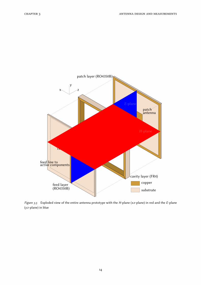
Figure 3: Exploded view of the entire antenna prototype withthe H-plane (xz-plane) in red and the E-plane (yz-plane) inblue
viii
D. Evaluation
The simulation and measurement results of the antennaelement are provided in the following paragraphs.
a) Reflection coefficient: The magnitude of the antenna’sinput reflection coefficient, |S11|, is displayed in fig. 4. Thecurve remains below −10 dB in the interval from 25.18 to32.53 GHz, yielding an impedance bandwidth of 7.35 GHz, or,equivalently, a fractional bandwidth of 25.8 %. One observes agood agreement between the simulated and measured curves.
20 22 24 26 28 30 32 34 36 38
−30
−20
−10
0
7.35GHz
frequency[GHz
]
|S11|[ dB
]
MeasuredSimulated
Figure 4: Plot of |S11| as a function of frequency for the patchantenna
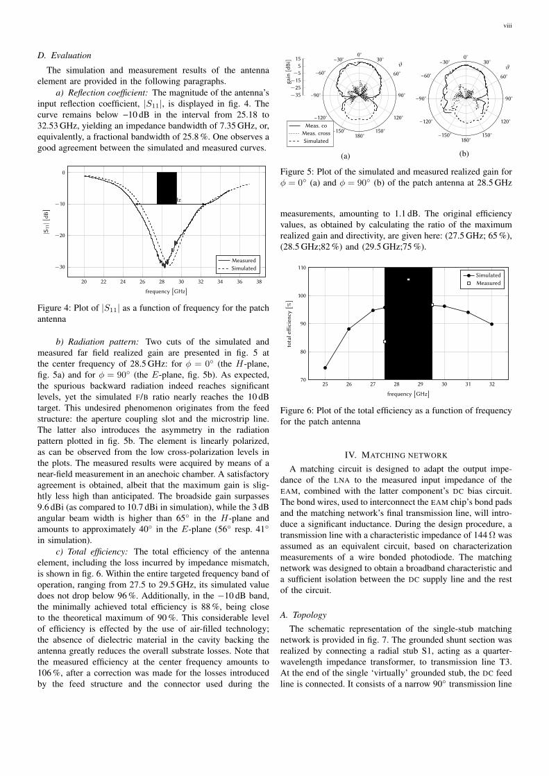
b) Radiation pattern: Two cuts of the simulated andmeasured far field realized gain are presented in fig. 5 atthe center frequency of 28.5 GHz: for φ = 0 (the H-plane,fig. 5a) and for φ = 90 (the E-plane, fig. 5b). As expected,the spurious backward radiation indeed reaches significantlevels, yet the simulated F/B ratio nearly reaches the 10 dBtarget. This undesired phenomenon originates from the feedstructure: the aperture coupling slot and the microstrip line.The latter also introduces the asymmetry in the radiationpattern plotted in fig. 5b. The element is linearly polarized,as can be observed from the low cross-polarization levels inthe plots. The measured results were acquired by means of anear-field measurement in an anechoic chamber. A satisfactoryagreement is obtained, albeit that the maximum gain is slig-htly less high than anticipated. The broadside gain surpasses9.6 dBi (as compared to 10.7 dBi in simulation), while the 3 dBangular beam width is higher than 65 in the H-plane andamounts to approximately 40 in the E-plane (56 resp. 41
in simulation).c) Total efficiency: The total efficiency of the antenna
element, including the loss incurred by impedance mismatch,is shown in fig. 6. Within the entire targeted frequency band ofoperation, ranging from 27.5 to 29.5 GHz, its simulated valuedoes not drop below 96 %. Additionally, in the −10 dB band,the minimally achieved total efficiency is 88 %, being closeto the theoretical maximum of 90 %. This considerable levelof efficiency is effected by the use of air-filled technology;the absence of dielectric material in the cavity backing theantenna greatly reduces the overall substrate losses. Note thatthe measured efficiency at the center frequency amounts to106 %, after a correction was made for the losses introducedby the feed structure and the connector used during the
0°30°
60°
90°
120°
150°180°
−150°
−120°
−90°
−60°
−30°
−35−25−15−5515
ϑ
gain
[dBi]
Meas. coMeas. crossSimulated
(a)
0°30°
60°
90°
120°
150°180°
−150°
−120°
−90°
−60°
−30°ϑ
(b)
Figure 5: Plot of the simulated and measured realized gain forφ = 0 (a) and φ = 90 (b) of the patch antenna at 28.5 GHz
measurements, amounting to 1.1 dB. The original efficiencyvalues, as obtained by calculating the ratio of the maximumrealized gain and directivity, are given here: (27.5 GHz; 65 %),(28.5 GHz;82 %) and (29.5 GHz;75 %).
25 26 27 28 29 30 31 3270
80
90
100
110
frequency[GHz
]
totaleiciency[ %]
SimulatedMeasured
Figure 6: Plot of the total efficiency as a function of frequencyfor the patch antenna
IV. MATCHING NETWORK
A matching circuit is designed to adapt the output impe-dance of the LNA to the measured input impedance of theEAM, combined with the latter component’s DC bias circuit.The bond wires, used to interconnect the EAM chip’s bond padsand the matching network’s final transmission line, will intro-duce a significant inductance. During the design procedure, atransmission line with a characteristic impedance of 144 Ω wasassumed as an equivalent circuit, based on characterizationmeasurements of a wire bonded photodiode. The matchingnetwork was designed to obtain a broadband characteristic anda sufficient isolation between the DC supply line and the restof the circuit.
A. Topology
The schematic representation of the single-stub matchingnetwork is provided in fig. 7. The grounded shunt section wasrealized by connecting a radial stub S1, acting as a quarter-wavelength impedance transformer, to transmission line T3.At the end of the single ‘virtually’ grounded stub, the DC feedline is connected. It consists of a narrow 90 transmission line

ix
Tf and a radial stub S2. The latter shorts the voltage sourceat 28.5 GHz, while the former converts this short circuit toan open at the point where the feed line is connected to thematching circuit. This way, the originally designed matchingperformance will not be jeopardized by the introduction of thebiasing circuit.
LNAT1,Z0 T2,Z0
bond
EAM
T3,Z0
Tf,ZfDC bias
DC feed
matching
T1 1.07mm 55.4°T2 2.00mm 103.6°T3 1.28mm 66.3°Tf 1.81mm 93.7°
S1 1.2mm 62.4°S2 1.2mm 62.4°
S2S1
Figure 7: Schematic of the matching network
B. Evaluation
The simulated scattering parameters of the matching net-work, obtained through full-wave electromagnetic simulation,are provided in fig. 8. The measured output impedance ofthe LNA was used as a reference for port 1, while the bondwire equivalent circuit in series with the measured EAM inputimpedance was connected to port 2. The circuit presents lowinsertion loss (below 0.7 dB in the system band) and providesadequate matching in the frequency band ranging from 25.5up to 32 GHz.
20 22 24 26 28 30 32 34 36 38
−30
−20
−10
0
frequency[GHz
]
|Sij|[ dB
]
|S11||S12||S21||S22|
Figure 8: Simulated scattering parameters of the matchingnetwork
V. SYSTEM
In a final step, the antenna was co-evaluated with theactive opto-electronic circuit. Figure 9 shows the schematic forsystem-oriented evaluation in Advanced Design System (ADS)Momentum. This allows for a verification of the functionality
antenna
interfaceLNA match
bond wire
EAM
Sij
Γin Γout
Figure 9: Schematic used to perform the system evaluationthrough co-simulation in ADS
of the entire receive chain, incorporating the measurementresults, obtained for each of the building blocks. The secondsimulation port uses the measured EAM scattering parametersas a reference, while the antenna reflection coefficient servesas a reference for the first. Observing the simulation results,plotted in fig. 10, it can be seen that the designed matchingcircuit provides an appropriate impedance conversion from thewire bonded EAM input to the LNA output over a wide fre-quency range. Indeed, the |S22| remains (well) below −10 dBfrom about 25 GHz, almost up to 32 GHz. At the input side, theLNA is not ideally matched to 50 Ω, while this was the targetfor the antenna input impedance, hence the suboptimal |S11|.Clearly, the forward gain and reverse isolation are dominatedby the LNA. Under the current circumstances, without furthermodification of the antenna input impedance, the systemperformance could still be optimized by tuning the length ofthe transmission line section connecting the antenna referenceport and the LNA input. A length of 4.4 mm was selected toobtain the results presented in fig. 10.
The antenna input impedance could now be tuned toobtain a better matching with the LNA, improving the overalltransmission toward the optical domain. While doing so, theaforementioned, additional transmission line section should ofcourse be taken into account.
20 22 24 26 28 30 32 34 36 38
−60
−40
−20
0
20
frequency[GHz
]
|Sij|[ dB
]
|S11||S12||S21||S22|
Figure 10: Co-simulation results of the system evaluation
The system noise figure was evaluated based on Friis’formula. Considering the high gain of the LNA and the lowinsertion loss of the subsequent stage, only the LNA itselfand the interface with the antenna element were taken intoaccount. In the operating frequency band, the insertion loss ofthe latter amounts to 0.52 dB at the highest, while the worstcase LNA noise figure is 2.7 dB, yielding a system noise figureapproximation of 3.22 dB. Additionally, the performance of

x
the receiver chain was assessed by simulating the transducerpower gain, which ranged between 24 to 26 dB, close to thegain realized by the LNA, using the schematic and data infigs. 9 and 10.
VI. CONCLUSION
A highly efficient antenna element was developed in theAFSIW technology for 5G communication in the 27.5 to29.5 GHz frequency band, providing a broadside realized gainof 9.6 dBi. It consists of a three-layered, stacked structurewith a patch antenna, an air-filled cavity and a microstripfeed line. The antenna was co-designed with active (LNA) andelectro-optical (EAM) components, leading to the developmentof a matching network with a broadband characteristic andintegrated DC biasing. The system performance was evaluatedin simulation through the scattering parameters of the receiverchain. Finally, a suggestion for future work was broughtup. The input impedance of the stand-alone antenna elementcould be modified so as to conjugately match the LNA’s inputimpedance and maximize power transmission.
REFERENCES
[1] F. Boccardi, R. W. Heath, A. Lozano, T. L. Marzetta,and P. Popovski, “Five disruptive technology directionsfor 5G”, IEEE Communications Magazine, vol. 52,no. 2, pp. 74–80, Feb. 2014, ISSN: 0163-6804. DOI:10.1109/MCOM.2014.6736746.
[2] S. Rinkel-Holgersson, “Optical fiber expansion and5G: Correlations and Synergie”, Digital Gipfel, Jun.2017, [Online]. Available: http : / / www - file . huawei .com/ - /media / CORPORATE / PDF / white % 20paper /white paper fiber 5g digital-summit en.pdf.
[3] Y. Niu, Y. Li, D. Jin, L. Su, and A. V. Vasilakos, “A sur-vey of millimeter wave communications (mmWave) for5G: opportunities and challenges”, Wireless Networks,vol. 21, no. 8, pp. 2657–2676, Nov. 2015, ISSN: 1572-8196. DOI: 10.1007/s11276-015-0942-z.
[4] A. Delmade, C. Browning, A. Farhang, N. Marchetti,L. E. Doyle, R. D. Koilpillai, L. P. Barry, and D. Ven-kitesh, “Performance analysis of analog IF over fiberfronthaul link with 4G and 5G coexistence”, IEEE/OSAJournal of Optical Communications and Networking,vol. 10, no. 3, pp. 174–182, Mar. 2018, ISSN: 1943-0620. DOI: 10.1364/JOCN.10.000174.
[5] G. P. Agrawal, Fiber-Optic Communication Systems,Fourth Edition. John Wiley & Sons, Inc, 2010, ISBN:9780470505113.
[6] Q. Van den Brande, S. Lemey, J. Vanfleteren, and H.Rogier, “Highly efficient impulse-radio ultra-widebandcavity-backed slot antenna in stacked air-filled substrateintegrated waveguide technology”, IEEE Transactionson Antennas and Propagation, vol. 66, no. 5, pp. 2199–2209, May 2018, ISSN: 0018-926X. DOI: 10.1109/TAP.2018.2809626.
[7] K. Y. Kapusuz, S. Lemey, and H. Rogier, “Substrate-Independent Microwave Components in Substrate In-tegrated Waveguide Technology for High-PerformanceSmart Surfaces”, IEEE Transactions on Microwave The-ory and Techniques, pp. 1–12, 2018, ISSN: 0018-9480.DOI: 10.1109/TMTT.2018.2823319.
[8] J. Mateo, A. M. Torres, A. Belenguer, and A. L. Borja,“Highly Efficient and Well-Matched Empty SubstrateIntegrated Waveguide H-Plane Horn Antenna”, IEEEAntennas and Wireless Propagation Letters, vol. 15,pp. 1510–1513, 2016, ISSN: 1536-1225. DOI: 10.1109/LAWP.2016.2516103.
[9] O. A. E. Caytan, L. Bogaert, H. Li, J. Van Kerrebrouck,S. Lemey, G. Torfs, J. Bauwelinck, P. Demeester, S.Agneessens, D. Vande Ginste, and H. Rogier, “PassiveOpto-antenna as Downlink Remote Antenna Unit forRadio Frequency over Fiber”, Journal of LightwaveTechnology, 2018, ISSN: 0733-8724. DOI: 10.1109/JLT.2018.2834153.
[10] Z. S. He, T. Lengyel, Y. Jian, M. Gavell, A. Larsson,and H. Zirath, “Optoelectronics Enabled Dense PatchAntenna Array for Future 5G Cellular Applications”, in2017 European Conference on Optical Communication(ECOC), Sep. 2017, pp. 1–3. DOI: 10 . 1109 / ECOC .2017.8346107.
[11] V. A. Thomas, M. El-Hajjar, and L. Hanzo, “Millimeter-Wave Radio Over Fiber Optical Upconversion Techni-ques Relying on Link Nonlinearity”, IEEE Communica-tions Surveys Tutorials, vol. 18, no. 1, pp. 29–53, Jan.2016, ISSN: 1553-877X. DOI: 10.1109/COMST.2015.2409154.
[12] A. M. Zin, M. S. Bongsu, S. M. Idrus, and N. Zulkifli,“An overview of radio-over-fiber network technology”,in International Conference On Photonics 2010, Jul.2010, pp. 1–3. DOI: 10.1109/ICP.2010.5604429.
[13] A. Dierck, F. Declercq, and H. Rogier, “Review ofactive textile antenna co-design and optimization strate-gies”, in 2011 IEEE International Conference on RFID-Technologies and Applications, Sep. 2011, pp. 194–201.DOI: 10.1109/RFID-TA.2011.6068637.
[14] A. Karttunen, A. F. Molisch, S. Hur, J. Park, andC. J. Zhang, “Spatially Consistent Street-by-Street PathLoss Model for 28-GHz Channels in Micro Cell UrbanEnvironments”, IEEE Transactions on Wireless Commu-nications, vol. 16, no. 11, pp. 7538–7550, Nov. 2017,ISSN: 1536-1276. DOI: 10.1109/TWC.2017.2749570.
[15] Rogers Corporation. (2017). RO4000 R© Series HighFrequency Circuit Materials, [Online]. Available: http:/ /www.rogerscorp.com/documents/726/acs/RO4000-LaminatesData-Sheet.pdf.

contents
Preface ii
Abstract iv
List of gures xiii
List of tables xv
List of abbreviations xv
1 Introduction 1
1.1 Context . . . . . . . . . . . . . . . . . . . . . . . . . . . . . . . . . . . . . . . . . . . . . 11.2 Goals and outline . . . . . . . . . . . . . . . . . . . . . . . . . . . . . . . . . . . . . . . 1
2 System specications 3
2.1 State of the art . . . . . . . . . . . . . . . . . . . . . . . . . . . . . . . . . . . . . . . . . 32.2 System architecture . . . . . . . . . . . . . . . . . . . . . . . . . . . . . . . . . . . . . . 42.3 Link budget . . . . . . . . . . . . . . . . . . . . . . . . . . . . . . . . . . . . . . . . . . 5
3 Antenna design and measurements 7
3.1 Requirements . . . . . . . . . . . . . . . . . . . . . . . . . . . . . . . . . . . . . . . . . 73.2 Concepts . . . . . . . . . . . . . . . . . . . . . . . . . . . . . . . . . . . . . . . . . . . . 7
3.2.1 Substrate integrated waveguides . . . . . . . . . . . . . . . . . . . . . . . . . . 73.2.2 Air-lled substrate integrated waveguide technology . . . . . . . . . . . . . . . 73.2.3 Cavity-backed patch antenna . . . . . . . . . . . . . . . . . . . . . . . . . . . . 83.2.4 Aperture coupling . . . . . . . . . . . . . . . . . . . . . . . . . . . . . . . . . . 9
3.3 Layout . . . . . . . . . . . . . . . . . . . . . . . . . . . . . . . . . . . . . . . . . . . . . 103.4 Connector and TRL calibration . . . . . . . . . . . . . . . . . . . . . . . . . . . . . . . . 153.5 Evaluation . . . . . . . . . . . . . . . . . . . . . . . . . . . . . . . . . . . . . . . . . . . 15
3.5.1 Simulation . . . . . . . . . . . . . . . . . . . . . . . . . . . . . . . . . . . . . . . 153.5.2 Sensitivity analysis . . . . . . . . . . . . . . . . . . . . . . . . . . . . . . . . . . 193.5.3 Measurements . . . . . . . . . . . . . . . . . . . . . . . . . . . . . . . . . . . . 22
4 Active and opto-electronic components 26
4.1 Low-noise amplier . . . . . . . . . . . . . . . . . . . . . . . . . . . . . . . . . . . . . . 264.1.1 Specications . . . . . . . . . . . . . . . . . . . . . . . . . . . . . . . . . . . . . 264.1.2 Design considerations . . . . . . . . . . . . . . . . . . . . . . . . . . . . . . . . 27
4.2 Electro-absorption modulator . . . . . . . . . . . . . . . . . . . . . . . . . . . . . . . . 274.2.1 Operation principle . . . . . . . . . . . . . . . . . . . . . . . . . . . . . . . . . . 284.2.2 Characterization measurements . . . . . . . . . . . . . . . . . . . . . . . . . . . 29
4.3 Matching circuit . . . . . . . . . . . . . . . . . . . . . . . . . . . . . . . . . . . . . . . . 304.3.1 First iteration . . . . . . . . . . . . . . . . . . . . . . . . . . . . . . . . . . . . . 324.3.2 Second iteration . . . . . . . . . . . . . . . . . . . . . . . . . . . . . . . . . . . . 33
xi

4.3.3 Encountered issues . . . . . . . . . . . . . . . . . . . . . . . . . . . . . . . . . . 354.4 Design of an evaluation board . . . . . . . . . . . . . . . . . . . . . . . . . . . . . . . . 374.5 Employed techniques . . . . . . . . . . . . . . . . . . . . . . . . . . . . . . . . . . . . . 37
4.5.1 Wire bonding . . . . . . . . . . . . . . . . . . . . . . . . . . . . . . . . . . . . . 374.5.2 Reow soldering . . . . . . . . . . . . . . . . . . . . . . . . . . . . . . . . . . . 38
4.6 Evaluation . . . . . . . . . . . . . . . . . . . . . . . . . . . . . . . . . . . . . . . . . . . 384.6.1 Simulation method . . . . . . . . . . . . . . . . . . . . . . . . . . . . . . . . . . 384.6.2 Measurements . . . . . . . . . . . . . . . . . . . . . . . . . . . . . . . . . . . . 39
5 System evaluation 40
5.1 Co-optimization strategies . . . . . . . . . . . . . . . . . . . . . . . . . . . . . . . . . . 405.2 Simulation . . . . . . . . . . . . . . . . . . . . . . . . . . . . . . . . . . . . . . . . . . . 405.3 Measurements . . . . . . . . . . . . . . . . . . . . . . . . . . . . . . . . . . . . . . . . . 44
6 Conclusion and future work 45
6.1 Conclusion . . . . . . . . . . . . . . . . . . . . . . . . . . . . . . . . . . . . . . . . . . . 456.2 Future work . . . . . . . . . . . . . . . . . . . . . . . . . . . . . . . . . . . . . . . . . . 45
Bibliography 47
A Appendix 50
xii

list of figures
2.1 Block diagram of the system . . . . . . . . . . . . . . . . . . . . . . . . . . . . . . . . . 4
3.1 Fringing electric elds as a radiation origin for microstrip patch antennas . . . . . . . . 93.2 Equivalent electric and magnetic polarization currents at an aperture in a conducting wall 103.3 Overview of common aperture shapes: rectangular, H-shape, bowtie and hourglass . . 103.4 Schematic representation of the antenna layout . . . . . . . . . . . . . . . . . . . . . . 133.5 Exploded view of the entire antenna prototype . . . . . . . . . . . . . . . . . . . . . . . 143.6 Recommended launch paern for a Southwest connector in combination with a micro-
strip line . . . . . . . . . . . . . . . . . . . . . . . . . . . . . . . . . . . . . . . . . . . . 153.7 Plot of |S11 | as a function of frequency for the patch antenna . . . . . . . . . . . . . . . 163.8 Smith chart plot of S11 for the patch antenna . . . . . . . . . . . . . . . . . . . . . . . . 173.9 Plot of the simulated realized gain for ϕ = 0° and ϕ = 90° for the patch antenna . . . . . 173.10 Plot of the angular beam width as a function of frequency for the patch antenna . . . . 183.11 Plot of the maximum realized gain and backward radiation level as a function of fre-
quency for the patch antenna . . . . . . . . . . . . . . . . . . . . . . . . . . . . . . . . . 183.12 Plot of the total eciency as a function of frequency for the patch antenna . . . . . . . 193.13 Eect of a 100 µm error on the cavity widthWcav of the patch antenna . . . . . . . . . . 203.14 Eect of a 100 µm error on the patch widthWpatch and length of Lpatch the patch antenna 203.15 Eect of a 100 µm error on the slot widthWslot of the patch antenna . . . . . . . . . . . 213.16 Eect of a 100 µm error on the slot length Lslot of the patch antenna . . . . . . . . . . . 213.17 Eect of a 50 µm error on the stub length Lstub of the patch antenna . . . . . . . . . . . 223.18 Plot of |S11 | as a function of frequency for the patch antenna, both measured and simulated 233.19 Smith chart plot of S11 for the patch antenna, both measured and simulated . . . . . . . 233.20 Plot of the measured and simulated realized gain for ϕ = 0° and ϕ = 90° of the patch
antenna . . . . . . . . . . . . . . . . . . . . . . . . . . . . . . . . . . . . . . . . . . . . . 25
4.1 Application circuit of the Analog Devices hmc1040 low-noise amplier . . . . . . . . . 264.2 Layout view of the lna evaluation board and resulting Smith chart plot of the measured
output reection coecient . . . . . . . . . . . . . . . . . . . . . . . . . . . . . . . . . . 274.3 Measured scaering parameters of the lna . . . . . . . . . . . . . . . . . . . . . . . . . 284.4 Red shi of the absorption band edge in a semiconductor due to the Franz-Keldysh eect 284.5 Smith chart plot of S11 for the eam with 0.6 V reverse bias and lumped component
equivalent circuit . . . . . . . . . . . . . . . . . . . . . . . . . . . . . . . . . . . . . . . 294.6 eam output power as a function of its reverse bias voltage . . . . . . . . . . . . . . . . 314.7 Block diagram of the measurement setup for the transmission measurements of the eam 314.8 Trajectory of the second version matching network on the Smith chart . . . . . . . . . 324.9 Schematic and layout of the rst version matching network . . . . . . . . . . . . . . . 334.10 Schematic and layout of the second version matching network . . . . . . . . . . . . . . 354.11 Simulated scaering parameters of the second version matching network . . . . . . . . 354.12 Evaluation of the isolation presented by the dc feed circuit . . . . . . . . . . . . . . . . 364.13 tdr waveform obtained for an rc shunt discontinuity . . . . . . . . . . . . . . . . . . . 374.14 Schematic representation of the circuit used to evaluate the matching network . . . . . 38
xiii

4.15 Plot of the simulated and measured scaering parameters for the rst version matchingnetwork . . . . . . . . . . . . . . . . . . . . . . . . . . . . . . . . . . . . . . . . . . . . 39
5.1 Layout view of the antenna element equipped with the active component footprints . . 415.2 Plot of |S11 | as a function of frequency for the stand-alone and integrated antenna . . . 425.3 Plot of the simulated realized gain for ϕ = 0° and ϕ = 90° for the stand-alone and
integrated antenna . . . . . . . . . . . . . . . . . . . . . . . . . . . . . . . . . . . . . . 425.4 Schematic used to perform the system evaluation through co-simulation in ads . . . . 425.5 Co-simulation results of the system evaluation in ads . . . . . . . . . . . . . . . . . . . 435.6 Simulated transducer gain of the receiver chain . . . . . . . . . . . . . . . . . . . . . . 44
A.1 Front and back of the realized patch antenna layer . . . . . . . . . . . . . . . . . . . . . 50A.2 Front and back of the realized microstrip feed layer . . . . . . . . . . . . . . . . . . . . 50A.3 Realized air-lled cavity layer . . . . . . . . . . . . . . . . . . . . . . . . . . . . . . . . 51A.4 Front and back of the assembled prototype . . . . . . . . . . . . . . . . . . . . . . . . . 51
xiv

list of tables
3.1 Relevant characteristics of the Rogers ro4350b substrate material . . . . . . . . . . . . 113.2 Dimensions of the cavity-backed patch antenna . . . . . . . . . . . . . . . . . . . . . . 123.3 Measured gain, angular beam width and total eciency of the patch antenna . . . . . . 24
4.1 Relevant characteristics of the Analog Devices hmc1040 low-noise amplier . . . . . . 26
xv

list of abbreviations
ac alternating current.ads Advanced Design System.afsiw air-lled substrate integrated waveguide.cst Computer Simulation Technology.cw continuous wave.dc direct current.dfb distributed feedback.eam electro-absorption modulator.edfa erbium doped ber amplier.f/b front-to-back.gcpw grounded coplanar waveguide.hemt high-electron-mobility transistor.ic integrated circuit.ip3 third-order intercept point.lna low-noise amplier.mimo multiple-input multiple-output.mzm Mach-Zehnder modulator.oma optical modulation amplitude.pcb printed circuit board.rf radio frequency.rof radio over ber.siw substrate integrated waveguide.snr signal-to-noise ratio.tdr time-domain reectometry.trl thru, reect, line.vna vector network analyzer.
xvi

1introduction
1.1 context
e h generation of wireless network technology is being developed as a response to the continuouslyincreasing demand for broadband access and the growing number of connected nodes accompanyingthe genesis of the Internet of ings. To meet the higher data rate and capacity requirements, whilemaintaining satisfactory reliability and low latency, architectural alterations are necessary. is meansthat incremental improvements of existing technologies will not suce to cope with these ever morestringent boundary conditions. A natural convergence of three major strategies arises: millimeterwave technology, smaller cell sizes and massive multiple-input multiple-output (mimo) [1]. Althoughpromising, the full potential of these technologies can only be unleashed through a multi-disciplinaryapproach in which the advantages of the optical and electrical domain are combined [2]. In section 2.1,the challenges and opportunities of an opto-electronic co-design procedure will be addressed, based ona critical review of the existing literature.
Millimeter waves open up more spectrum real estate, mitigating the adverse eects of the crowdedfrequency bands that are currently being used for communication. However, these high frequencysignals introduce more challenging propagation conditions. is property can nonetheless prove tobe benecial, as it allows for a higher degree of frequency reuse and suppresses interference betweencells. e combination of millimeter waves and smaller cells thus accommodates a greater number ofhigh-mobility users [3]. ese cells will be equipped with numerous remote antenna heads connectedto the larger base stations [4]. Of course, this will require a compact integration of signal amplicationand electro-optical modulation in these units, as the back-end communication is to be provided byoptical ber, ensuring very high bandwidths and low losses [5]. Consequently a co-optimization of theantenna on the one hand and the active and opto-electronic components on the other hand is necessary,severely complicating the design procedure and making proper signal handling crucial.
1.2 goals & outline
e design and realization of an active, electro-optical receiver antenna for 5g communication in the27.5 to 29.5 GHz frequency band is targeted. e eventual goal of this thesis is to design the variousbuilding blocks or select commercially available components and combine them into a fully functionalactive receiver antenna. First an foremost, this requires the creation of an ecient antenna element, forwhich the air-lled substrate integrated waveguide (siw) technology has been selected. For the signalamplication, a commercial low-noise amplier (lna) is chosen. e opto-electronic component, anelectro-absorption modulator (eam), was included in a design of the IDLab research group and has beenmade available for this thesis. An eective matching network is to be designed, adapting the inputimpedance of the eam to the output impedance of the lna. A major challenge is to properly integrateall of these building blocks on the antenna element, while maintaining compatibility with the employedmanufacturing techniques and optimizing the performance.
Aer extensive simulation and optimization, the various components of the design are manufacturedand validated separately. To this end, a range of measurements is executed, enabling a thoroughcomparison of the simulation results versus the performance of the realized prototypes. e extracted
1

chapter 1 introduction
parameters provide valuable information to construct an eective co-optimization strategy, which couldeventually lead to the realization of an operational, electro-optically integrated antenna head. In aparallel master thesis, by Igor Lima de Paula, an equivalent transmier antenna was designed [6]. eultimate objective would be to set up a communication link between the realized transmit and receiveantenna heads.
In chapter 2, the state of the art in this domain is discussed, leading to realistic specications for thebuilding blocks, as described in the system architecture. An analysis of the link budget will demonstratethe adequacy of these requirements. Chapter 3 treats the development of the stand-alone antennaprototype, shedding light on the employed theoretical concepts and providing measurement resultsvalidating its performance. e other building blocks, to be integrated on the back of this antennaelement, are introduced in chapter 4. An overview of all of these components is provided, along with adescription of the design and measurement procedures, where applicable. In chapter 5, the system designstrategy is unfolded and simulation results for the operation of the entire system are demonstrated.Finally, this work is concluded in chapter 6 and suggestions for future research are supplied.
2

2system specifications
2.1 state of the art
In this section, a few of the anticipated challenges during the development of the system are addressedand the proposed solutions are investigated in the existing literature. e antenna prototype is designedin the air-lled siw technology and employs electro-optical co-design to cope with the challengingenvironment described in section 1.1. It is aimed at deployment in a radio over ber (rof) system, as aremote antenna head connected to a central base station.
Various structures employing the air-lled substrate integrated waveguide (afsiw) technologyhave been reported, including a Ku-band horn antenna [7]. e design methodology of these typicallymultilayered structures and a transition frommicrostrip is covered in [8]. Likewise, a few articles analyzethe expected properties of this technology, followed by an investigation of the eects of fabricationtolerances and parameter variations. Also, results on prototypes of afsiw components have beenpublished, for instance on the development of an ultra-wideband cavity-backed slot antenna [9] orother microwave components with uncommon substrate materials [10]. An important challenge inthis thesis will be to scale and adapt these ndings to much higher frequencies, while maintaining theperformance.
An additional major diculty when creating an opto-electronic wireless receiver is the integrationof the antenna element(s) and active components. Low system loss and a limited noise gure are desired,which imposes stringent requirements on the performance of the electrical-to-optical conversion. Notonly must the optical input power be suciently high, the employed modulator must oer an elevatedmodulation eciency, while coping with these high input power levels. An example of a photonicallyintegrated patch antenna is presented in [11]. Its stacked design is carefully devised to enable thedeployment of an eciently radiating structure onto a wafer of ‘photonic material’. More extensivediscussions can be found in [12] and [13]. e former article, published as part of the sandra project,oers a description of the entire system and the development of specic components. e laer targetsa more fundamental approach for the integration of optical techniques. Both, however, consider opticalbeamforming as a noteworthy research topic. A system level overview is oered in [14], whereas [15]examines the design procedure of a concrete opto-electronic radio frequency (rf) front-end. A proof ofconcept for an active, electro-optical patch antenna array is demonstrated in [16].
In this context, rof is oen cited as a key enabler in the evolution toward higher operatingfrequencies and smaller cell sizes [17], [18]. It allows to deploy low-complexity remote antenna heads,that are only required to perform conversion between the electrical and optical domains. e signalmanagement tasks, on the other hand, can be centralized in a control station. In [19], such a remoteopto-antenna unit for rof applications is demonstrated. e usage of optical communication entails highbandwidth, low transmission losses and lile rf interference. However, these systems are inherentlynonlinear and will therefore limit the aainable noise performance and dynamic range. Moreover,chromatic and modal dispersion are bound to occur, as an optical ber does not present a frequency-atchannel [5].
Finally, designing a fully and compactly integrated active opto-electronic antenna also requires awell-considered co-design strategy. Two distinct methods are proposed in [20]: (a) matching the antennaimpedance to the input impedance of the integrated active device or (b) using a matching network to
3

chapter 2 system specifications
adapt the active component’s optimum impedance to the 50Ω environment. In either of these twocases, joint circuit and full-wave simulation procedures were invoked. Starting with the developmentof the active device in Advanced Design System (ads), the circuit simulator can be utilized for lumpedcomponents, while Momentum is deployed for simulating passive interconnects. Subsequently, theantenna structure can be dened in Computer Simulation Technology (cst) Microwave Studio. A naloptimization is performed by linking both simulators together.
2.2 system architecture
A block diagram, schematically representing all constituents of the electro-optical receiver antenna, isshown in g. 2.1.
LNA match
EAMCW laser
Figure 2.1 Block diagram of the system
e receiver front-end consists of a wideband antenna element (g. 3.5), serving as a platformfor compact integration with active and opto-electronic components, to reduce the losses due tointerconnection to a minimum. e dimensions of the structure allow to t the aforementionedcomponents on the back of the antenna element itself. An lna amplies the incoming signals fromthe receiver antenna, without severely aecting the noise performance of the chain. Subsequently, theelectrical signals are converted to the optical domain by means of an eam. A detailed description ofthis device is postponed to section 4.2. With ever increasing bitrates — as imposed by the evolutiontoward the h generation of wireless communication — direct modulation of a laser no longer remainsa suitable means of encoding information, because of the introduced frequency chirp. Consequently,external optical modulation is employed in this thesis, by manipulating continuous wave (cw) lightfrom a laser with constant bias. e input impedance of the eam is matched to the output impedanceof the lna, which is close to 50Ω, by means of a matching network. Together with the active andopto-electronic components, this matching network is to be integrated on the antenna head itself.Further signal processing can then be performed in a single base station to which multiple remoteantenna heads connect.
e initial aim is to develop a stand-alone antenna element that is at rst well-matched to 50Ω atthe center frequency of the receiver, f0 = 28.5 GHz, for validation purposes. An impedance bandwidthof 2GHz is targeted, covering the frequency band ranging from 27.5 to 29.5 GHz, as this range is atpresent actively researched and several experimental deployments are being executed. e antenna’seciency should preferably be as high as possible. To this end, an afsiw technology implementationwill be realized; a more detailed description of this technology can be found in section 3.2.2. Additionally,
4

chapter 2 system specifications
the antenna element should be suciently robust, ensuring a proper cooperation of the integratedcomponents, by realizing an elevated front-to-back (f/b) ratio. is also ensures a stable antennaoperation aer integration in a realistic deployment platform. e path loss is proportional to the squareof the operating frequency, rendering its eects more apparent for millimeter waves. At a distance ofjust 25m, the line-of-sight loss already amounts to 90 dB and even higher values are reported in real lifeenvironments [21]. Consequently, the loss should be counteracted by optimizing the antenna elementfor a high realized gain (as an addition to the gain provided by the lna). e resulting beam shouldhowever remain suciently wide to leave the option open of adapting the element to include it in anarray.
2.3 link budget
To enable a proper assessment of the receiver chain’s performance in a later stage, some key parametersare investigated beforehand, on a system level, based on the available data of the selected buildingblocks [22].
e rst property to be investigated is the noise gure, a quantity that expresses the degradation ofthe signal-to-noise ratio (snr). It is dened as:
NF = 10 log10 F with F =SNRinSNRout
(2.1)
To nd the equivalent noise factor F of several cascaded devices, one can invoke Friis’ formula:
F = F1 +F2 − 1G1
+F3 − 1G1G2
+ · · · +Fn − 1
G1G2 · · ·Gn−1, (2.2)
where Fn and Gn are the noise factor and (linear) power gain of the n-th device.e noise gure will dictate the required gain in the receiver chain, as it aects the sensitivity and
hence the minimum detectable signal. e power spectral density of the noise received by the antennaimposes a fundamental lower limit on the required signal power. Modeling the noise source as a resistor,one nds:
Pn,out = kT · BW = 4 × 10⁻²¹W/Hz · BW
= −174 dBm/Hz + 10 log10 BWat 290 K (2.3)
e sensitivity, being the minimum detectable signal level at the input of the receiver chain, cannow be dened using the enhanced noise power (as described by the noise gure) and the required snrat the output:
Si [dBm] = −174 dBm/Hz + 10 log10 BW + NF [dB] + SNRout [dB] (2.4)
From the above discussion, one would conclude that the lna gain should be boosted as muchas possible, to limit the eect produced by the added noise in the later stages. A second importantcharacteristic should, however, be taken into account as well, namely linearity. is puts an upperlimit on the allowable amplier gain, as the output signal must saturate neither the subsequent stages,nor the lna itself. A common quantity to express the linearity of a system is the third-order interceptpoint (ip3). It is dened as the theoretical point in a two-tone measurement where the intermodulationproducts at 2f1 − f2 and 2f2 − f1 are equal in power to the fundamental tones f1 and f2. An expressionsimilar to eq. (2.2) exists to calculate the global, input-referred ip3:
1PIIP3
=1
PIIP3,1+
G1PIIP3,2
+G1G2PIIP3,3
+ · · · +G1G2 · · ·Gn−1
PIIP3,n(2.5)
5

chapter 2 system specifications
In this thesis, lile room for improvement of the key performance parameters will be le aerthe selection of the active and opto-electronic components. e suciently high lna gain will renderthe added noise by the subsequent blocks in the chain negligible. Nonetheless, an aempt is made toquantify the system noise gure based on the evaluation results in chapter 5. Considering the linearity:this will only be aected by the lna and the eam. Since the laer component is xed for this thesis andthe former is selected to be highly linear, the only remaining concern will be to limit the input powernot to drive the receiver head into nonlinear operation.
6

3antenna design and measurements
3.1 reqirements
e general system specications, as introduced in section 2.2, will now be expressed in a morequantitative fashion. e feasibility of the imposed requirements can be estimated by analyzing theperformance parameters of current state-of-the-art designs, as found in the literature.
Adequate matching of the antenna element to the 50Ω system impedance is ensured by imposingthat |S11 | < −10 dB within the system band. With this upper limit on the magnitude of the reectioncoecient, at most 10 % of the power submied to the antenna is reected. As it is oen the case, atrade-o between the realized gain and beam width will have to be accepted. erefore, a relativelyconservative value for both parameters is proposed. It is desired to aain a realized gain exceeding10 dBi, while maintaining a beam width of at least 45° both in the E-plane and the H -plane (see g. 3.5).To steer as much power as possible into the forward hemisphere of the antenna, a f/b ratio of at least10 dB is envisioned. e air-lled antenna element should aain an eciency of at least 95 % over theentire frequency band of interest.
3.2 concepts
In this section, some of the concepts underlying the design of the antenna element are discussed. eidea behind traditional dielectric-lled siw technology is demonstrated and contrasted with its air-lledcounterpart. Next, the operation principle of a (cavity-backed) patch antenna is briey touched upon,while introducing the relevant design equations. To conclude, aperture coupling is treated, along with amotivation for the choice of this feeding mechanism and its implications on the nal layout.
3.2.1 Substrate integrated waveguides
e siw technology was developed to translate traditional rectangular waveguides to an equivalentthat is compatible with printed circuit board (pcb) manufacturing processes. e conducting sidewallsof the rectangular waveguide are replaced by rows of vias embedded in the substrate, connecting theparallel metal plates of the board. e resulting structure presents a highly planar aspect, as opposed tothe original, while maintaining the desirable properties, such as an elevated quality factor. However, itis imperative that the vias be placed suciently close together, to limit the radiative leakage. Otherwise,the equivalence between classical and substrate integrated rectangular waveguides does not hold,prohibiting the use of the well-known equations for the electromagnetic elds. Nonetheless, one shouldtake into account that the eective width of the waveguide is always somewhat higher, as the elds doextend slightly between the vias.
3.2.2 Air-lled substrate integrated waveguide technology
Afsiw components oer signicant benets with respect to their dielectric-lled counterparts, aslosses in the structures are reduced on three levels. First and foremost, they are designed such that theelectromagnetic elds are primarily conned within the air-lled cavity, thus avoiding the dielectriclosses that would occur in regular substrates. Furthermore, the cavity walls can now be realized in solid
7

chapter 3 antenna design and measurements
copper, rather than as rows of vias, by performing round-edge plating aer milling the air-lled cavity.is results in lower losses due to undesired radiation. Finally, the conductor losses, caused by coppersurface roughness, are mitigated. In air-lled cavities, the outer surface has to be considered, which canbe polished to a much greater smoothness [9].
Additionally, the air-lled nature of the cavity renders its performance largely independent of theactual substrate material used in the surrounding pcb. One might therefore substitute expensive rfsubstrate materials – normally required for high-frequency applications – by a low-cost alternativelike fr4. As a consequence, the aforementioned performance improvements can even be realized in acost-eective fashion.
e promise of high eciency, combined with its relatively economical character, renders the afsiwtechnology an ideal candidate in aempting to aain the eciency goal stipulated in section 3.1, whilemaintaining the suitability for usage in a large number of remote antenna heads.
3.2.3 Cavity-backed patch antenna
A microstrip patch antenna is constructed by aaching a metallic sheet to a dielectric substrate (relativepermiivity ϵr) with a ground plane at the boom. As this substrate material can be of limited thickness(usually much smaller than the operating wavelength), microstrip antennas are generally low-proleand, especially at high frequencies, relatively compact. Consequently, they are ideally adapted tointegration with other circuits in applications for which space is of limited availability, such as mobilecommunication devices [23].
e structure can be considered as a leaky resonating cavity, that radiates through the fringingelds that extend into the substrate and air beyond the patch edges. is phenomenon is illustratedschematically in g. 3.1. e initial size of the patch antenna was determined based on the well-established design formulas [24]:
W =v02f0
√2
ϵr + 1(3.1)
L =1
2f0√ϵr,e√ϵ0µ0
− 2∆L (3.2)
where the low-frequency approximation for the eective relative permiivity ϵr,e is given by:
ϵr,e =ϵr + 12 +
ϵr − 12
(1 + 12h
W
)− 12
withW h (3.3)
Due to fringing eects, the electrical length of the patch antenna exceeds its physical dimension. is isaccounted for in eq. (3.2), by subtracting 2∆L, invoking the following frequently used design equation:
∆L = 0.412h(ϵr,e + 0.3)
(W
h+ 0.264
)
(ϵr,e − 0.258)(W
h+ 0.8
) (3.4)
e air-lled cavity was dimensioned to be square with a width of approximately one wavelength inair at the center frequency. e resonant frequency of the TEmn0 mode in the air-lled cavity can bedetermined based on:
fmn0 =c
2π√ϵr
√(mπ
Wcav
)2+
(nπ
Lcav
)2(3.5)
8

chapter 3 antenna design and measurements
is sizing resulted in a relatively large aperture alongside the patch edges and hence a directive antenna.Although this design choice renders the element less adapted to deployment in an array conguration,it does result in a superior gain (see g. 3.9), meeting the requirement dened earlier.
εr
Figure 3.1 Fringing electric fields as a radiation origin for microstrip patch antennas
3.2.4 Aperture coupling
e resonant cavity backing the microstrip patch antenna is fed by a microstrip line, coupling theelectromagnetic elds through an aperture. At frequencies ranging up to almost 30GHz, this feedingtechnique is preferred over alternatives such as coaxial probe feeds, as the former results in a higherimpedance bandwidth. Moreover, an accurate, secure connection of a coaxial cable would be dicult.
Another advantage of this feeding technique is that it, too, enables practical integration with activeelectronics. ey can be positioned on the same substrate as the feed line and be directly connected toit, eciently using the available space. A coaxial probe feed can also provide this advantage, yet it isless cost-eective and more labor-intensive to implement.
Unfortunately, as a consequence of the coupling from the microstrip feed line to the air-lled cavityvia an aperture, signicant backward radiation can be expected. A f/b ratio of at least 10 dB is, however,targeted, lest the active circuitry be aected. By maximizing the coupling in the forward direction, therisk of destabilizing the lna, for instance, is reduced. As the coupling level is principally determined bythe coupling slot, this is achieved by selecting its dimensions small enough such that the backwardradiation is manageable and the impedance matching of the antenna is feasible [25].
e physical mechanism underlying aperture coupling can be demonstrated by representing the slotas an electric and magnetic dipole [26]. An intuitive, visual explanation of this statement is provided ing. 3.2. e lemost drawings show the normal electric eld E and the tangential magnetic eld H neara conducting surface. When a small aperture is added to the wall, one observes the fringing of the eldsthrough it, illustrated in the central gures. Comparing these paerns to the elds induced by smallelectric and magnetic polarization currents Pe and Pm (as shown on the right-hand side of g. 3.2), theresemblance of (b) and (c) resp. (e) and (f) indicates that the proposed equivalent model is valid. As themagnitudes of these currents are proportional to the elds inducing them, they can be expressed as:
Pe = αeϵ0Enδ (r − r0) (3.6)
Pm = −αmHtδ (r − r0) (3.7)
For a rectangular slot, the proportionality constants are αe = αm = πWL2/16, withW and L the widthand length of the coupling slot.
e electric and magnetic current sources that can now be used to calculate the excited modes inthe cavity are then given by:
J = jωPe (3.8)
M = jωµ0Pm (3.9)
9
chapter 3 antenna design and measurements
Coupling aperture
Couplingaperture Ground
plane
Waveguide
Stripline
Microstrip1
Microstrip 2
Waveguide1
Feedwaveguide
Cavity
Waveguide2
(a) (b)
(d)(c)
r
r r
FIGURE 4.29 Various waveguide and other transmission line configurations using aperture cou-pling. (a) Coupling between two waveguides via an aperture in the common broadwall. (b) Coupling to a waveguide cavity via an aperture in a transverse wall.(c) Coupling between two microstrip lines via an aperture in the common groundplane. (d) Coupling from a waveguide to a stripline via an aperture.
Consider Figure 4.30a, which shows the normal electric field lines near a conductingwall (the tangential electric field is zero near the wall). If a small aperture is cut into theconductor, the electric field lines will fringe through and around the aperture as shownin Figure 4.30b. Now consider Figure 4.30c, which shows the fringing field lines aroundtwo infinitesimal electric polarization currents, Pe, normal to a conducting wall (without
(a)
(d)
H
n
(c)(b)
E Pe
Pm
(e) (f)
n
ˆ
ˆ
FIGURE 4.30 Illustrating the development of equivalent electric and magnetic polarization cur-rents at an aperture in a conducting wall. (a) Normal electric field at a conductingwall. (b) Electric field lines around an aperture in a conducting wall. (c) Elec-tric field lines around electric polarization currents normal to a conducting wall.(d) Magnetic field lines near a conducting wall. (e) Magnetic field lines near anaperture in a conducting wall. (f) Magnetic field lines near magnetic polarizationcurrents parallel to a conducting wall.
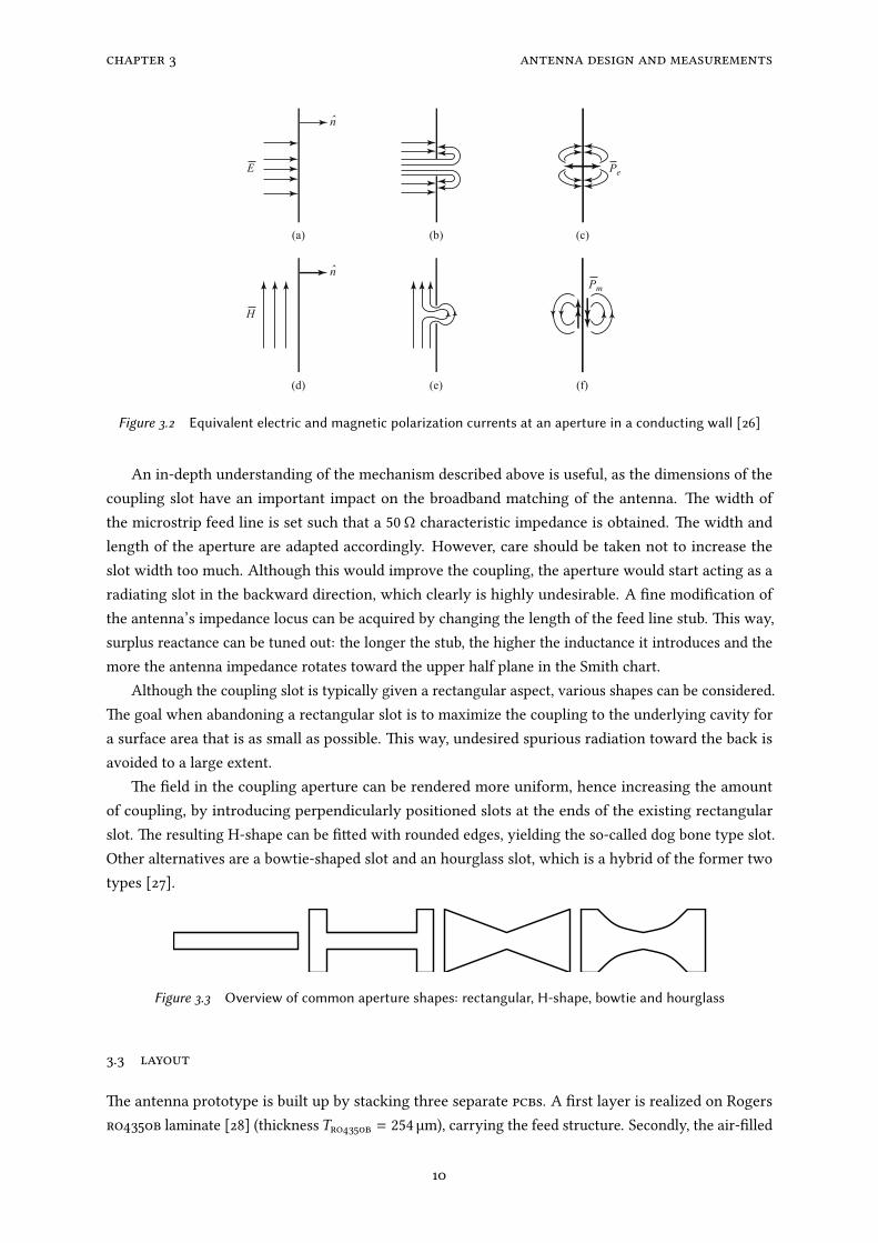
Figure 3.2 Equivalent electric and magnetic polarization currents at an aperture in a conducting wall [26]
An in-depth understanding of the mechanism described above is useful, as the dimensions of thecoupling slot have an important impact on the broadband matching of the antenna. e width ofthe microstrip feed line is set such that a 50Ω characteristic impedance is obtained. e width andlength of the aperture are adapted accordingly. However, care should be taken not to increase theslot width too much. Although this would improve the coupling, the aperture would start acting as aradiating slot in the backward direction, which clearly is highly undesirable. A ne modication ofthe antenna’s impedance locus can be acquired by changing the length of the feed line stub. is way,surplus reactance can be tuned out: the longer the stub, the higher the inductance it introduces and themore the antenna impedance rotates toward the upper half plane in the Smith chart.
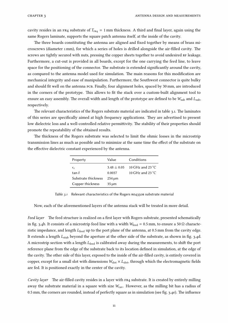
Although the coupling slot is typically given a rectangular aspect, various shapes can be considered.e goal when abandoning a rectangular slot is to maximize the coupling to the underlying cavity fora surface area that is as small as possible. is way, undesired spurious radiation toward the back isavoided to a large extent.
e eld in the coupling aperture can be rendered more uniform, hence increasing the amountof coupling, by introducing perpendicularly positioned slots at the ends of the existing rectangularslot. e resulting H-shape can be ed with rounded edges, yielding the so-called dog bone type slot.Other alternatives are a bowtie-shaped slot and an hourglass slot, which is a hybrid of the former twotypes [27].
Figure 3.3 Overview of common aperture shapes: rectangular, H-shape, bowtie and hourglass
3.3 layout
e antenna prototype is built up by stacking three separate pcbs. A rst layer is realized on Rogersro4350b laminate [28] (thicknessTro4350b = 254 µm), carrying the feed structure. Secondly, the air-lled
10
chapter 3 antenna design and measurements
cavity resides in an fr4 substrate of Tfr4 = 1mm thickness. A third and nal layer, again using thesame Rogers laminate, supports the square patch antenna itself, at the inside of the cavity.
e three boards constituting the antenna are aligned and xed together by means of brass mi-croscrews (diameter 1mm), for which a series of holes is drilled alongside the air-lled cavity. escrews are tightly secured with nuts, pressing the copper sheets together to avoid undesired rf leakage.Furthermore, a cut-out is provided in all boards, except for the one carrying the feed line, to leavespace for the positioning of the connector. e substrate is extended signicantly around the cavity,as compared to the antenna model used for simulation. e main reasons for this modication aremechanical integrity and ease of manipulation. Furthermore, the Southwest connector is quite bulkyand should t well on the antenna pcb. Finally, four alignment holes, spaced by 30mm, are introducedin the corners of the prototype. is allows to t the stack over a custom-built alignment tool toensure an easy assembly. e overall width and length of the prototype are dened to beWsub and Lsub,respectively.
e relevant characteristics of the Rogers substrate material are indicated in table 3.1. e laminatesof this series are specically aimed at high frequency applications. ey are advertised to presentlow dielectric loss and a well-controlled relative permiivity. e stability of their properties shouldpromote the repeatability of the obtained results.
e thickness of the Rogers substrate was selected to limit the ohmic losses in the microstriptransmission lines as much as possible and to minimize at the same time the eect of the substrate onthe eective dielectric constant experienced by the antenna.
Property Value Conditions
εr 3.48± 0.05 10GHz and 23 Ctan δ 0.0037 10GHz and 23 CSubstrate thickness 254 µmCopper thickness 35 µm
Table 3.1 Relevant characteristics of the Rogers ro4350b substrate material
Now, each of the aforementioned layers of the antenna stack will be treated in more detail.
Feed layer e feed structure is realized on a rst layer with Rogers substrate, presented schematicallyin g. 3.4b. It consists of a microstrip feed line with a widthWfeed = 0.5mm, to ensure a 50Ω characte-ristic impedance, and length Lfeed up to the port plane of the antenna, at 0.5mm from the cavity edge.It extends a length Lstub beyond the aperture at the other side of the substrate, as shown in g. 3.4d.A microstrip section with a length Lfeed is calibrated away during the measurements, to shi the portreference plane from the edge of the substrate back to its location dened in simulation, at the edge ofthe cavity. e other side of this layer, exposed to the inside of the air-lled cavity, is entirely covered incopper, except for a small slot with dimensionsWslot × Lslot, through which the electromagnetic eldsare fed. It is positioned exactly in the center of the cavity.
Cavity layer e air-lled cavity resides in a layer with fr4 substrate. It is created by entirely millingaway the substrate material in a square with sizeWcav. However, as the milling bit has a radius of0.5mm, the corners are rounded, instead of perfectly square as in simulation (see g. 3.4e). e inuence
11
chapter 3 antenna design and measurements
of this approximation is expected and simulated to be negligible, as the strength of the electromagneticelds is very low in this area of the cavity. e vertical edges of the cavity are covered with a copperlayer, by means of round-edge plating. At both sides, the remainder of the board also consists of copper.
Patch layer On a second layer of Rogers material, the microstrip patch antenna is manufactured. It islocated precisely above the middle of the resonating cavity backing it. e length Lpatch of the patch,along the direction of the E-eld, dictates its resonance frequency; the width is chosen to be identical tothe length. e remainder of this side of the substrate is also covered in copper, except for a squarewith a size equal to the dimensions of the underlying cavity, surrounding the patch. In contrast, all thecopper is removed from the outward facing side of this layer.
e dimensions of the nal design are summarized in table 3.2, while a schematic representation ofthe layout is given in g. 3.4. A top view of the patch antenna layer and the layer supporting the feedstructure is provided, together with a cross section of the complete pcb stack along the feed line. Notethat the z-dimension of the laer drawing was stretched by a factor of 10. A representation of the nalantenna prototype is provided in g. 3.5 and pictures of the realized antenna layers and the assembledprototype can be found in appendix A.
Parameter Value [mm]
Wcav 11.50 = 1.09λ0Lcav 11.50 = 1.09λ0Lpatch 2.95 = 0.28λ0Wslot 2.55 = 0.27λ0Lslot 0.55 = 0.05λ0Lstub 0.20 = 0.02λ0Lfeed 20 = 1.90λ0Wsub 34.50 = 3.27λ0Lsub 43.50 = 4.12λ0Tro4350b 0.254 = 0.02λ0Tfr4 1 = 0.09λ0
Table 3.2 Dimensions of the cavity-backed patch antenna
Remark: For the transmit (parallel thesis by Igor Lima de Paula [6]) and receive (this work) side,two separate, though very similar antenna designs were created. Both prototypes rely on the sameoperating principle. Electromagnetic elds are coupled to an air-lled cavity through an aperture inthe feed layer. is cavity resonates and backs a microstrip patch antenna. e distinction betweenboth designs resides in the dimensions of the cavity and the layout of the feed structure. e receiverprototype is ed with a microstrip feed line and has a relatively large cavity (about one wavelengthsquared), rendering it somewhat more directive than its transmier counterpart with a groundedcoplanar waveguide (gcpw) feed and more modest cavity dimensions. More specically, the formerelement is optimized for maximum gain and impedance bandwidth, while the other can be employed ina phased array thanks to its smaller dimensions and larger beam width.
12

chapter 3 antenna design and measurements
Wcav
Lpatch
Lsub
Wsub
(a)
Lfeed
Wsub
fixing hole
y
x
slot contour
reference plane
(b)
Tro4350b
Tfr4
Tro4350b2× Tcopper
Lcav
Lslot
Lpatchz
y
(c)
Wslot
LslotLstub
Wfeed
(d)
air-filled cavitysubstratecopperround-edge copper platingsimulated copper plating
(e)
Figure 3.4 Schematic representation of the antenna layout: top view of the patch layer (a) and the feed layer(b), a cross section along the feed line (c) and details of the microstrip feed line with aperture coupling slot (d)and the cavity corners with round-edge plating (e)
13
chapter 3 antenna design and measurements
patch layer (RO4350B)
patchantenna
cavity layer (FR4)
substrate
copper
yx z
feed layer(RO4350B)
feed line toactive components
coupling slot
E-plane
H -plane
Figure 3.5 Exploded view of the entire antenna prototype with the H-plane (xz-plane) in red and the E-plane(yz-plane) in blue
14

chapter 3 antenna design and measurements
Figure 3.6 Recommended launch paern for a Southwest connector in combination with a microstrip line
3.4 connector & trl calibration
To link the measurement equipment to the antennas under test, 1.85mm end launch connectors,manufactured by Southwest Microwave, are used [29]. ey are specically designed to be ed andremoved easily, require no soldering and can thus be reused. e connection is made by clamping theconnector onto the board with a specied amount of force. e supplier provides an optimized launchpaern, with a tapered ending, to compensate for the capacitance introduced by the connector pin. erecommended layout is shown in g. 3.6.
To validate through measurement the antenna input impedance at the simulated reference plane,the feed structure and connector should be calibrated away. First of all, the connector should bepositioned suciently far from the antenna under test, to avoid any adverse inuence due to itspresence. Furthermore, the eects of the feed line and connector can be removed from the measuredscaering parameters by performing a so-called thru, reect, line (trl) calibration. To this end, acustom kit was designed to move the reference plane right up to the edge of the resonant cavity, as insimulation. e reect standard is a shorted microstrip line with a length equal to that of the antennafeed line up to the reference plane (Lfeed). e thru standard is a microstrip line, double the length ofthe reect, while the line standard is additionally 90° longer at the center frequency of 28.5 GHz. esespecications were submied to the vector network analyzer (vna), enabling the device to calculatethe scaering parameters of the error network (consisting of the coaxial cables, end launch connectorsand microstrip feed lines) and to shi the port reference plane of the measurements to the appropriateposition.
An alternative to the aforementioned approach is to perform the de-embedding oine. To this end,the vna is calibrated up to and including the coaxial measurement cables, by means of the electroniccalibration kit. Subsequently, the scaering parameters of the custom calibration standards and thedevice under test are recorded with this setup. A trl algorithm, implemented in e.g. the Python packagescikit-rf [30], is then applied to the acquired data. is approach can be advantageous because itallows for a more extensive control over the de-embedding and requires the custom calibration kit tobe measured only once.
3.5 evaluation
3.5.1 Simulation
e design and simulation of the antenna prototypes were performed using cst Microwave Studio.A model was created based on the initial, theoretical sizing described in section 3.2.3 and the layoutoverview oered in section 3.3. An extensive optimization cycle was then started, modifying the designparameters to obtain a conguration that yielded a high impedance bandwidth, satisfactory gain and asuciently high f/b ratio. e simulation results of this eort are provided in the gures discussed in
15

chapter 3 antenna design and measurements
the following paragraphs. An impedance bandwidth of 6.82GHz is obtained, comfortably covering thetargeted band of 27.5 to 29.5 GHz. e maximum realized gain is expected to be 10.7 dBi, while the 3 dBbeam width amounts to 56° resp. 41° in the H -plane and E-plane. e f/b ratio nearly reaches the 10 dBtarget in the frequency band of interest. Finally, the total eciency surpasses 96 %.
Reection coecient e magnitude of the antenna’s input reection coecient, |S11 |, is displayed ing. 3.7. e curve remains below −10 dB in the interval from 25.76 to 32.58GHz, yielding an impedancebandwidth of 6.82GHz, or, equivalently, a fractional bandwidth of 23.9 %. A minimum is reached at28.77GHz, where |S11 | = −29.4 dB.
20 22 24 26 28 30 32 34 36 38
−30
−20
−10
0
6.82GHz
frequency[GHz
]
|S11|[ dB
]
Figure 3.7 Plot of |S11| as a function of frequency for the patch antenna
On the Smith chart, g. 3.8, one observes that the antenna characteristic consists of a resonanceloop around the center, with a small additional ‘notch’ at 28.5 GHz. Widening the air-lled cavityrotates the locus clockwise, while an increase in the patch length rotates the aforementioned notchcounterclockwise, thus causing a frequency shi. Finally, modications of the slot width and lengthintroduce a simultaneous rotation and alter the shape of the notch. It becomes more pronounced whenevolving from a narrower to a wider coupling slot, eventually realizing an additional loop.
Radiation paern Two cuts of the simulated far eld realized gain are presented in g. 3.9 at the centerfrequency of 28.5 GHz: for ϕ = 0° (the H -plane, g. 3.9a) and for ϕ = 90° (the E-plane, g. 3.9b). Asexpected, the spurious backward radiation indeed reaches signicant levels. is undesired phenomenonoriginates from the feed structure: the aperture coupling slot and the microstrip line. e laer alsointroduces the asymmetry in the radiation paern ploed in g. 3.9b.
Figure 3.10 illustrates the variation of the angular beam width as a function of the frequency, againfor both E-plane and H -plane. In the former cut of the far eld realized gain, the beam width variesfrom 39.3° to 44.8° within the −10 dB band. For the laer section, the values range from 53.2° to 61.9°.e relatively narrow beam is a consequence of the large cavity dimensions, compared to the microstrippatch size. is makes the antenna less suited for use in a classical array conguration, as it will giverise to grating lobes. More specically, in an array with uniformly spaced antenna elements, positionedtoo far apart, radiation will occur in directions other than the one of the intended main lobe. For a
16

chapter 3 antenna design and measurements
0.2 0.5 1 2 50
0.2
0.5
1
2
5
−0.2
−0.5−1
−2
−5
20GHz28.5GHz35GHz
Figure 3.8 Smith chart plot of S11 for the patch antenna
0°30°
60°
90°
120°
150°180°
−150°
−120°
−90°
−60°
−30°
−15−10−5051015
ϑ
gain
[dBi]
(a)
0°30°
60°
90°
120°
150°180°
−150°
−120°
−90°
−60°
−30°ϑ
(b)
Figure 3.9 Plot of the simulated realized gain for φ = 0° (a) and φ = 90° (b) for the patch antenna
17

chapter 3 antenna design and measurements
given maximum beam steering angle θmax and wavelength λ, the element spacing should not exceedthe following value [31]:
dmax <λ
1 + sin |θmax |(3.10)
Nonetheless, this more directive antenna element would be well-adapted to be employed in apoint-to-point link.
25 26 27 28 29 30 31 32
40
50
60
70
frequency[GHz
]
3dBbeam
width
[ °]
φ = 0° (sim.)φ = 90° (sim.)φ = 0° (meas.)φ = 90° (meas.)
Figure 3.10 Plot of the angular beam width as a function of frequency for the patch antenna, both in the E-plane(φ = 90°) and the H-plane (φ = 0°)
e variation of the maximum far eld realized gain and the backward radiation levels with thefrequency is demonstrated in g. 3.11. Within the system band, the gain aains a high and stable value,ranging between 10.4 and 10.7 dBi. e f/b ratio is at least 9.2 dB and aains values up to 10.2 dB, closeto the original target.
25 26 27 28 29 30 31 32
0
2
4
6
8
10
frequency[GHz
]
gain
[ dBi]
Realized gain (sim.)Back radiation levelRealized gain (meas.)
Figure 3.11 Plot of the maximum realized gain and backward radiation level as a function of frequency for thepatch antenna
18

chapter 3 antenna design and measurements
Total eciency e total eciency of the antenna element, including the loss incurred by impedancemismatch, is shown in g. 3.12. Within the entire targeted frequency band of operation, ranging from27.5 to 29.5 GHz, its value does not drop below 96 %. Additionally, in the −10 dB band, the minimallyachieved total eciency is 88 %, being close to the theoretical maximum of 90 %. Obviously, the totaleciency reduces rapidly outside of the frequency band of interest, where the signicantly lower valuecan be ascribed to the return loss resulting from inferior impedance matching. is considerable level ofeciency is eected by the use of air-lled technology; the absence of dielectric material in the cavitybacking the antenna greatly reduces the overall substrate losses.
25 26 27 28 29 30 31 3270
80
90
100
110
frequency[GHz
]
totaleiciency[ %]
SimulatedMeasured
Figure 3.12 Plot of the total eiciency as a function of frequency for the patch antenna
3.5.2 Sensitivity analysis
In the modeling soware, dimensions can be set to a very high precision, enabling extensive optimizationto obtain the desired performance. In real life, however, one must take into account a few unavoidabledeviations. At higher frequencies, manufacturing tolerances become ever more critical, as the magnitudeof the potential deviations gets larger with respect to the wavelength. It is therefore advisable toinvestigate the inuence of inaccuracies in some key parameters of the antenna design, thus assessingits robustness. e primary possible error for this antenna topology is incorrect manufacturing of thetrack widths (due to under-etching during the isotropic removal of copper). Other approximations inthe simulator are related to the relative permiivity of the substrate, the copper roughness and the(vacuum) environment.
e cavity dimensions — width and length both equal toWcav — appear to be of lile inuence onthe antenna performance. Even though variations of up to 200 µm were considered, the only eect onthe simulated |S11 | is a slight alteration of the curve’s minimum (see g. 3.13). is insensitivity can beexplained considering the dimensions of the cavity relative to the wavelength. As long as the variationscan be deemed of small proportions in the electrical sense, their inuence will remain limited.
e patch size Lpatch is expected to be the most critical parameter, as it primarily determines theresonance frequency of the antenna. From eqs. (3.1) and (3.2), it is evident that a size reduction willlead to an increase in resonant frequency and vice versa. In g. 3.14, one indeed observes that a 100 µmdeviation, irrespective of the sign, results in a detuning of the antenna amounting to several hundredsof megahertz.
19

chapter 3 antenna design and measurements
20 22 24 26 28 30 32 34 36 38
−30
−20
−10
0
frequency [GHz]
|S11| [dB
]
WcavWcav − 200 µmWcav + 100 µm
Figure 3.13 Eect of a 100 µm error on the cavity width Wcav of the patch antenna
20 22 24 26 28 30 32 34 36 38
−30
−20
−10
0
frequency [GHz]
|S11| [dB
]
WpatchWpatch − 100 µmWpatch + 100 µm
Figure 3.14 Eect of a 100 µm error on the patch width Wpatch and length Lpatch of the patch antenna
20

chapter 3 antenna design and measurements
Figures 3.15 and 3.16 show the inuence of variations in the widthWslot and length Lslot of theaperture coupling slot. Again, the matching of the structure is somewhat compromised when deviatingfrom the reference design. Moreover, mode bifurcation [9] occurs, caused by the widening of the slot,which essentially starts acting as an additional antenna at the rear side of the cavity-backed patch.When a tight coupling exists between both radiating structures, the resonant modes will separate andundergo a frequency shi. is phenomenon is clearly visible for theWslot + 100 µm design. To avoidthis from happening, one should make sure that the electric eld of the patch antenna remains wellenclosed by the air-lled cavity. Otherwise, the occurring fringing elds increase the coupling with theaperture, with the aforementioned undesired frequency shi as a result.
20 22 24 26 28 30 32 34 36 38
−30
−20
−10
0
frequency [GHz]
|S11| [dB
]
WslotWslot − 100 µmWslot + 100 µm
Figure 3.15 Eect of a 100 µm error on the slot width Wslot of the patch antenna
20 22 24 26 28 30 32 34 36 38
−30
−20
−10
0
frequency [GHz]
|S11| [dB
]
LslotLslot − 100 µmLslot + 100 µm
Figure 3.16 Eect of a 100 µm error on the slot length Lslot of the patch antenna
Finally, variations in the microstrip feed line extension (Lstub) beyond the aperture were analyzed.For this parameter, variations of only ±50 µm considered. Nonetheless, a signicant inuence on thequality of the matching is observed in g. 3.17.
21

chapter 3 antenna design and measurements
20 22 24 26 28 30 32 34 36 38
−30
−20
−10
0
frequency [GHz]
|S11| [dB
]
LstubLstub − 50 µmLstub + 50 µm
Figure 3.17 Eect of a 50 µm error on the stub length Lstub of the patch antenna
3.5.3 Measurements
Figure 3.7 shows a plot of the antenna’s simulated |S11 | without extended substrate and xing screws.To obtain a valid comparison between simulated and measured results, however, a second simulationwas performed. is time, the model included a cylindrical approximation of the brass bolts and nuts.One could observe that the additional features, external to the original antenna model, barely aectedthe performance, such that the global trend of the original characteristic was well maintained.
An important disadvantage of the relatively thin Rogers substrate became evident during themeasurements. As the trace width of a 50Ω line scales down along with the substrate thickness, thealignment of the Southwest connector’s central conductor gets more critical. Initial severely deviatingmeasurement results suggested to closely verify all congurations and the entire measurement setup.is revealed that there was some tolerance in the connector’s positioning holes, resulting in a possiblyinaccurate alignment with the feed line. As a consequence, a careful review under the microscopeproved necessary.
As the rst measurement resulted in some aphysical behavior, a second aempt was carried out.is time, particular aention was paid to a proper calibration of the vna. During the characterizationof the trl kit, the same two Southwest connectors remained aached to the measurement cables andwere repositioned for each of the calibration standards. is way, any potential deviation between theavailable connectors was eliminated. Observing the results in gs. 3.18 and 3.19, one notices a very closeagreement between the measured and simulated data. Since only four xing screws were employed, asopposed to the original twelve in the preliminary simulation, no adverse eects are visible whatsoever.
Finally, the radiation paerns of the antenna were measured by means of a spherical near eld setupin an anechoic chamber. e realized gain was calibrated by matching the near eld data to a far eldmeasurement with a standard gain horn at a specied distance of the prototype. In g. 3.20, simulationand measurement are compared in the H -plane (ϕ = 0°) and the E-plane (ϕ = 90°), for the lower, centerand upper frequency of the system band, being 27.5, 28.5 and 29.5 GHz respectively. e measuredcross-polarization data is provided as well, demonstrating the linear polarization of the antenna. Notethat data were acquired only for elevation angles in the range ϑ ∈ [−135°, 135°]. For a valid comparison
22

chapter 3 antenna design and measurements
20 22 24 26 28 30 32 34 36 38
−30
−20
−10
0
7.35GHz
frequency[GHz
]
|S11|[ dB
]
MeasuredSimulated
Figure 3.18 Plot of |S11| as a function of frequency for the patch antenna, both measured and simulated
0.2 0.5 1 2 50
0.2
0.5
1
2
5
−0.2
−0.5−1
−2
−5
20GHz35GHz
Figure 3.19 Smith chart plot of S11 for the patch antenna, both measured and simulated
23

chapter 3 antenna design and measurements
with the simulated results, the model including xing screws and an extended substrate was employedthis time, contrary to the plots in g. 3.9. is way, a satisfactory agreement is obtained, albeit that themaximum gain is slightly less high than anticipated. Furthermore, the curve appears less smooth inthe forward direction of the H -plane cuts. e broadside realized gain, the 3 dB angular beam widthfor both far eld cuts and the total eciency are summarized in table 3.3 at the three investigatedfrequencies. ese measured values are compared to the simulation results in gs. 3.10 to 3.12. Notethat he measured eciency at the center frequency surpasses 100%, aer a correction was made for thelosses introduced by the feed structure and the connector used during the measurements, amounting to1.1 dB. e original eciency values, as obtained by calculating the ratio of the maximum realized gainand directivity, are given here: (27.5 GHz; 65 %), (28.5 GHz; 82 %) and (29.5 GHz; 75 %).
Frequency [GHz] Gain [dBi] @ ϑ = 0° 3 dB beam width [°] Total eiciency [%]φ = 0° φ = 90°
27.5 7.56 69 53 83.6 %28.5 9.63 68 37 105.8 %29.5 8.41 65 41 96.7 %
Table 3.3 Measured gain, angular beam width and total eiciency of the patch antenna
24
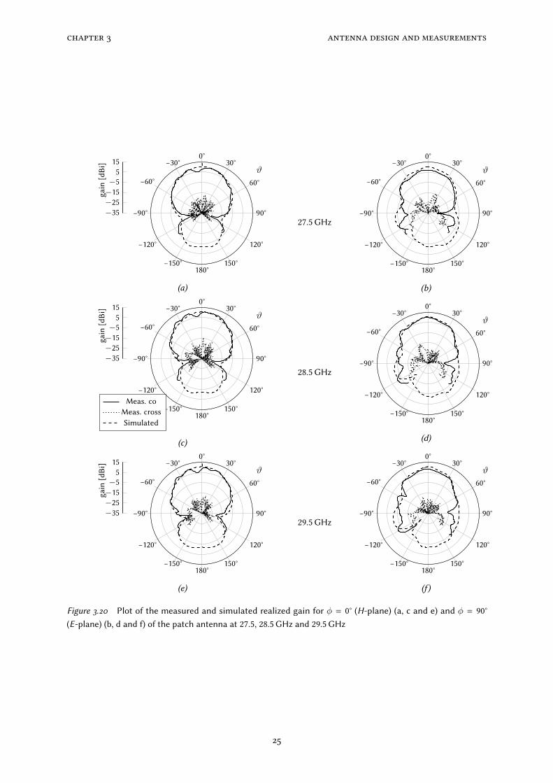
chapter 3 antenna design and measurements
0°30°
60°
90°
120°
150°180°
−150°
−120°
−90°
−60°
−30°
−35−25−15−5515
ϑ
gain
[dBi]
(a)
27.5GHz
0°30°
60°
90°
120°
150°180°
−150°
−120°
−90°
−60°
−30°ϑ
(b)0°
30°
60°
90°
120°
150°180°
−150°
−120°
−90°
−60°
−30°
−35−25−15−5515
ϑ
gain
[dBi]
Meas. coMeas. crossSimulated
(c)
28.5GHz
0°30°
60°
90°
120°
150°180°
−150°
−120°
−90°
−60°
−30°ϑ
(d)
0°30°
60°
90°
120°
150°180°
−150°
−120°
−90°
−60°
−30°
−35−25−15−5515
ϑ
gain
[dBi]
(e)
29.5GHz
0°30°
60°
90°
120°
150°180°
−150°
−120°
−90°
−60°
−30°ϑ
(f)
Figure 3.20 Plot of the measured and simulated realized gain for φ = 0° (H-plane) (a, c and e) and φ = 90°(E-plane) (b, d and f) of the patch antenna at 27.5, 28.5GHz and 29.5GHz
25

4active and opto-electronic components
4.1 low-noise amplifier
4.1.1 Specications
For the lna, a commercial component was selected, based on the requirements dened in chapter 2.e most suitable candidate proved to be the hmc1040 by Analog Devices [32]. Its relevant propertiesare listed in table 4.1. e component realizes a satisfactory gain, while keeping the noise gure withinacceptable limits and obtaining sucient linearity.
Property Value
Gain 23 dBNoise figure 2.2 dBOutput power for 1 dB compression 12 dBmOutput third order intercept (oip3) 22 dBm
Table 4.1 Relevant characteristics of the Analog Devices hmc1040 low-noise amplifier
e suggested application circuit in the hmc1040 datasheet is shown in g. 4.1. e 3 × 3mm packageprovides three separate supply pins, that should all be set to the same voltageVdd1 = Vdd2 = Vdd3 = 2.5 V.e rfin and rfout ports are direct current (dc) blocked and internally matched to 50Ω.
For price, delivery and to place orders: Hittite Microwave Corporation, 2 Elizabeth Drive, Chelmsford, MA 01824Phone: 978-250-3343 Fax: 978-250-3373 Order On-line at www.hittite.com
Application Support: Phone: 978-250-3343 or [email protected]
Am
pli
fie
rs
- l
ow
No
ise
- s
mT
5
HMC1040LP3CEv00.0112
GaAs pHEMT MMIC LOW NOISEAMPLIFIER, 24 - 43.5 GHz
Pin Descriptions
Capacitor Value
C1 - C3 100 pf
C4 - C6 10 nf
C7 - C9 4.7 µf
Pin Number function Description interface schematic
1, 2, 4, 9, 11, 12
GNDThese pins and package bottom must
be connected to RF/DC ground.
3 rfiNThis pin AC coupled
and matched to 50 ohms
5-8, 14 N/CThe pins are not connected internally; however, all data
shown herein was measured with these pins connected to rf/DC ground externally.
10 rfoUTThis pin AC coupled
and matched to 50 ohms
13, 15, 16 Vdd3, Vdd2, Vdd1Drain bias voltages for the amplifier. See Application Circuit
for required external componnets.
Application Circuit
Information furnished by Analog Devices is believed to be accurate and reliable. However, no responsibility is assumed by Analog Devices for its use, nor for any infringements of patents or other rights of third parties that may result from its use. Specifications subject to change without notice. No license is granted by implication or otherwise under any patent or patent rights of Analog Devices. Trademarks and registered trademarks are the property of their respective owners.
For price, delivery, and to place orders: Analog Devices, Inc., One Technology Way, P.O. Box 9106, Norwood, MA 02062-9106 Phone: 781-329-4700 • Order online at www.analog.com Application Support: Phone: 1-800-ANALOG-D
Figure 4.1 Application circuit of the Analog Devices hmc1040 low-noise amplifier [32]
At the heart of the lna resides a pseudomorphic high-electron-mobility transistor (hemt), a eld-eect transistor containing a GaAs heterojunction. e main advantages of these components are thehigh frequency capabilities, up to millimeter wave frequencies, high gain and low noise. Obviously,this makes them ideally suited to be used in lnas for e.g. mobile and satellite communication. e‘pseudomorphic’ specication refers to the alignment of materials with slightly dierent laice constants.is is realized by employing a very thin layer of one of both materials in the heterojunction, such thatthe laice simply extends or compresses to t the other one. As discontinuities are avoided this way,the performance of the device is not adversely aected [33].
26

chapter 4 active and opto-electronic components
4.1.2 Design considerations
As the remote antenna head, in which this lna is integrated, is exposed to the elements, a vericationof its properties’ temperature stability is desirable. e datasheet indicates an increased noise gure,lower gain and worse linearity for rising temperatures. However, all of these trends are expected andthe deviation remains within reasonable limits.
e manufacturer supplied scaering parameters to be used in simulation. It appeared, however,that they incorporate the microstrip feed lines used on the evaluation board proposed in the datasheet.For the design of the matching network, accurate and trustworthy data on the performance of thelna are of paramount importance. erefore, an additional characterization of the lna was carriedout, using a custom-designed board, the layout of which is displayed in g. 4.2a. It is realized on thesame ro4350b laminate with a thickness of 254 µm as the outer layers of the antenna element, as areall other evaluation boards discussed in the following sections. is would allow for a convenientintegration of the designed boards for the active and opto-electronic components on the feed layer ofthe antenna, without a need for modications due to a dierent substrate material or thickness. On theevaluation board, a footprint is provided for the lna and for the decoupling capacitors alike. Like for theantenna measurements, Southwest end launch connectors were utilized as an rf interface; appropriateland paerns and mounting holes are provided. A plot of the measured S22 scaering parameter isshown on the Smith chart in g. 4.2b, as it is most relevant for this thesis. e full scaering parametercharacterization is provided in g. 4.3. e device is adequately matched to the 50Ω system impedance(|S11 |, |S22 | < −10 dB) and provides a forward gain |S21 | exceeding 24.5 dB within the system band. Toobtain these results, the measurement reference plane was shied up to the pads at either side of thelna footprint by means of a trl calibration.
(a)
0.2 0.5 1 2 50
0.2
0.5
1
2
5
−0.2
−0.5−1
−2
−5
28.5GHz
20GHz37GHz
(b)
Figure 4.2 Layout view of the lna evaluation board and resulting Smith chart plot of the measured outputreflection coeicient
4.2 electro-absorption modulator
e eam used for this thesis was included in a design of the IDLab research group and fabricated by imec.Characterization measurements were performed for a variety of bias voltages, optical input powers andwavelengths.
27

chapter 4 active and opto-electronic components
20 22 24 26 28 30 32 34 36 38
−60
−40
−20
0
20
frequency[GHz
]
|Sij|[ dB
]
|S11||S12||S21||S22|
Figure 4.3 Measured scaering parameters of the lna
4.2.1 Operation principle
e operation of an eam is based on the Franz-Keldysh eect, which describes the eective band gapdecrease of a semiconductor under the inuence of an applied electrical eld. As a consequence, atransparent material might start absorbing light if the correct conditions are satised, and it could thusbe used as a means to modulate a light source of constant intensity. is eect is oen referred to asphoton-assisted tunneling, as it relies on the overlap between the electron and hole wave functions,extending in the band gap, to allow the absorption of a photon with energy lower than the band gapenergy Eg [5]. An illustration of the so-called red shi experienced by the absorption spectrum is givenin g. 4.4.
λ1 λ2
α1
α2
∆α∆λ
wavelength
absorption
Figure 4.4 Red shi of the absorption band edge in a semiconductor due to the Franz-Keldysh eect
is kind of modulator oers a high modulation bandwidth (in the order of tens of gigahertz) andallows for complete photonic integration with a distributed feedback (dfb) laser. With respect to directmodulation, a larger extinction ratio and lower frequency chirp can be expected.
28

chapter 4 active and opto-electronic components
An alternative external modulator is based on a Mach-Zehnder interferometer. is device consistsof two arms, dividing the supplied light into two paths, that result in either constructive or destructiveinterference. To this end, the optical paths are equipped with a phase shier. e phase dierence isrealized by creating an electro-optical refractive index change, resulting in a modied eective opticalpath length. In case of perfect dierentially steered Mach-Zehnder modulator (mzm), only the intensityof the light is modulated, not its phase, and no frequency chirp is present at all [5].
Nonetheless, an eam exhibits more desirable features for rof links. First of all, its structure is muchmore compact than an mzm and does not require a 50Ω termination, which is benecial in terms ofpower consumption. Moreover, eams can also be employed as a photodiode.
During operation, the device is biased with a reverse voltage in the order of −1 to −2V and drivenby a modulation voltage with an amplitude of 1 to 2Vp−p.
4.2.2 Characterization measurements
In g. 4.5c, a lumped component equivalent circuit of the eam is devised. e physical structure of thedevice is almost identical to the one of a photodiode, except for the doping of the chip’s semiconductormaterial. In reverse bias, it can be modeled by its junction capacitance with a series resistance. Toaccount for the bond pads and the interconnection to the actual component, some additional lumpedcomponents were added to the schematic. Like for the antenna measurements, the measurementequipment was calibrated out. To this end, custom calibration standards were available. In this case, theinterfacing with the bare optical chip was performed by means of appropriate electrical probes, havinga pitch equal to the one of the bond pads. e resistance and capacitance values were determined bying the simulated reection coecient as a function of frequency to the measured curves, a sample ofwhich is shown in g. 4.5a for a reverse bias of 0.6 V, together with the characteristic of the equivalentcircuit.
0.2 0.5 1 2 50
0.2
0.5
1
2
5
−0.2
−0.5−1
−2
−528.5GHz
MeasuredEquivalent
(a)
Component Value
R1 1 kΩ
R2 65.5Ω
R3 2.2 kΩ
C1 45.3 fFC2 34.8 fF
(b)
C1
R1
R2
C2 R3
(c)
Figure 4.5 Smith chart plot of S11 for the eam with 0.6V reverse bias (a) and lumped component equivalentcircuit (c) with numeric values (b)
29

chapter 4 active and opto-electronic components
In order to nd out which performance specications the other components in the chain shouldmeet, a transmission characterization proved to be useful. By means of a ber probe, cw laser lightwas coupled into the bare eam chip via one of its facets. e modulated light at the output facetwas captured again, amplied by means of an erbium doped ber amplier (edfa) and subsequentlyconverted to the optical domain by means of a photodiode. e actual transmission |S21 |, from theelectrical, modulating input signal to the output signal of the photodiode, was determined using avna. A theoretical characteristic of the output power as a function of the eam’s reverse bias voltageis shown in g. 4.6, while a block diagram of the described measurement setup is provided in g. 4.7.One observes that a higher reverse bias results in a lower output power. Furthermore, it can be seenthat the highest modulation eciency can be reached when the device is driven in the quasi-linearsection of the P(V )-characteristic. A more detailed analysis of the optimum bias point will be givenin the next paragraph. Another expected trend is an increased bandwidth for stronger reverse bias.is can be explained if the eam is modeled as a varactor, the capacitance of which decreases with theapplied negative voltage. Overall, the higher the reverse bias, the ‘aer’ the curve representing |S21 |should become: lower in power and more extended in bandwidth. However, in spite of several lengthyyet fruitless aempts, no valid data could successfully be acquired. e observed transmission onlyaained very low values (in the order of −40 dB) and the aforementioned eects could not be observed.
Starting from a xed average input power, it is desired to nd the maximum output optical mo-dulation amplitude (oma). By choosing a bias point, the voltage swing related to the electrical inputpower yields a higher and lower optical output power level P1 and P0. Aer dening the extinctionratio re = P1/P0 and the average output power Pav = (P0 + P1)/2, the oma is then given by:
OMA = P1 − P0 = 2Pavre − 1re + 1
(4.1)
Based on the the responsivity of the photodiode used to detect the eam’s optical power, a photocur-rent and hence an electrical output power can be derived, again related to the chosen bias point andmodulating voltage.
Note that in a nal design, the laser source could be integrated on the eam chip. However, thisimprovement is not straightforward. A laser cannot be realized in a traditional silicon process, as thissubstrate material does not provide optical gain. erefore, incorporating the laser source would requirethe integration of a iii-v material in silicon. Additionally, the optical output could be realized with amore permanent connector. As a consequence, the intricate alignment procedure would not be neededany longer. Moreover, excessive losses introduced by the coupling facets would be avoided, i.e. edgecouplers (1 dB loss) would replace the grating couplers (6 dB loss).
An evaluation board was designed to assess the performance of the eam by itself. It consists ofa gcpw transmission line section, to be calibrated away, and a cavity in which the bare chip couldbe embedded. e interconnection between the bond pads on the one hand and the ground planeand signal trace on the other hand was intended to be realized through wire bonding. However, dueto the limited availability of eam chips, it was decided not to devote an instance to this board but tocharacterize the bare die and the system evaluation board as a whole.
4.3 matching circuit
Amatching circuit is required to adapt the output impedance of the lna to themeasured input impedanceof the eam with bond wire. To enhance compactness and limit the bond wire length, the eam’s dc
30

chapter 4 active and opto-electronic components
opticalo
utpu
tpo
wer
reverse bias voltage
bias point
P1
P0
Figure 4.6 eam output power as a function of its reverse bias voltage
pd pd bias
laser edfaeam
vnaeam bias
rfdcoptic
Figure 4.7 Block diagram of the measurement setup for the transmission measurements of the eam
bias circuit is combined with this matching circuit. e wire bonding, used to interconnect the chip’sbond pads and the matching network’s nal transmission line, will introduce a signicant inductance.Obviously, this aects the optimization of the matching network. During the design procedure, a bondwire inductance of 1 nH was assumed at rst. Later on, an alternative equivalent was devised based onmeasurement results. It was found that the matching performance is quite sensitive to variations in thebond wire length: changes of just 100 µm up- or downward severely counteract the desired eect of thematching network.
When designing a matching network, the principle of conjugate matching is applied. Consequently,the maximum amount of power is delivered from the generator to the load. is can be demonstratedby considering the power transmied by a generator with output impedance Zg = Rg + jXg to a loadZ` = R` + jX` :
P =|Vg |
2
2R`
(R` + Rg)2 + (X` + Xg)2(4.2)
e power P can be maximized by dierentiating eq. (4.2) with respect to the real and imaginaryparts R` and X` of Z` and equating both to zero. Solving the resulting set of equations then nallyyields:
R` = Rg and X` = −Xg (4.3)
31

chapter 4 active and opto-electronic components
In other words: the impedance of the load, observed at the generator, should be the complex conjugateof the generator output impedance. For Z` = Z ∗g , the power delivered to the load is P = |Vg |2/8Rg [22].
e single-stub tuning technique is employed to achieve the conjugate matching goal. e resultingmatching circuit consists of a transmission line with an open- or short-circuited stub aached to it,either in series or in parallel. One can vary both the stub’s length (to realize the required impedance) andits distance with respect to the load. First, a stretch of 50Ω transmission line rotates the load impedancearound the center of the Smith chart, until it resides on the constant resistance circle corresponding tothe real part of the generator impedance. e stub then provides the required reactance to convert theload impedance to the conjugate of the generator impedance [34].
By opting for such a simple conguration, the matching bandwidth is kept as high as possible,while limiting the introduced losses, in a robust implementation. Multisection matching networks couldyield more bandwidth, but the tolerance to manufacturing deviations is signicantly higher and thusundesired for this thesis.
Note that the matching network aempts to adapt the eam’s input impedance to the complexconjugate of the lna’s output impedance directly, without intermediately passing through the 50Ωsystem impedance. e output impedance of the lna, though designed and measured to be matchedrelatively well to 50Ω, does present a slightly higher resistance and some inductive reactance. eenvisioned trajectory, realized by the nal version of the matching network (see g. 4.10a), is presentedon the Smith chart in g. 4.8.
0.2 0.5 1 2 50
0.2
0.5
1
2
5
−0.2
−0.5−1
−2
−5Zeam
Z∗lna
Figure 4.8 Trajectory of the second version matching network on the Smith chart
e dc bias of the eam must be integrated into the matching network, as the ports of the lna aredc blocked. Consequently, a bias voltage supplied by the equipment used during measurements (e.g.the vna) cannot be passed through the amplier to the eam.
4.3.1 First iteration
In a premature phase of the design, the matching circuit consisted of two transmission line stubs. ebond wire inductance was estimated to be around 550 nH, which proved to be too optimistic. For thedc bias of the eam, two options were considered and made available on the physical board design. edc current would be owing either through a large inductance (with suciently high self-resonance
32

chapter 4 active and opto-electronic components
frequency), to be considered an open circuit at the operating frequency, or through a quarter-wavelengthtransmission line, which would also present an open at its exact resonance frequency. erefore, thealternating current (ac) operation would be aected in neither of the two described cases. For theprototypes to be produced, it was nonetheless preferred to incorporate the bias circuit into the matchingnetwork, as described in the following paragraphs.
An initial, manufactured version of the matching network again consisted of a transmission linesection and a single grounded stub, terminated by a tapered section. At its end, a narrow trace connectedthe dc supply, acting as an rf choke inductance. Furthermore, the trace served the purpose of isolatingthe voltage source from the rest of the circuit, such that the inuence on its envisioned performancecould be neglected. Originally, the transmission line stub was supposed to be grounded by meansof a capacitor, acting as a short at the operating frequency while presenting an open circuit at dc.However, the use of a lumped component with a suciently high self-resonance frequency appeared tobe unrealistic. erefore, the matching network was characterized without including the capacitor.
At the end of the dc feed line, a suciently large patch was provided to allow for easy solderingof a wire, connecting to the supply by means of a crocodile clamp. An alternative approach would beto provide the footprint of an appropriate connector and to solder it on the board. is way, the usedwires could be (dis)connected whenever desired.
A schematic of this rst version matching network is given in g. 4.9a, while the layout is providedin g. 4.9b. Details on the additional features in the layout are provided in section 4.3.2, as they weremaintained in the second iteration. Simulation and measurements results are shown in g. 4.15.
LNAT1,Z0 T2,Z0
bond
EAM
T3,Z0
Tf,Zf
DC bias
T1 1.73mm 89.5°T2 1.23mm 63.7°T3 1.26mm 65.2°Tf 2.00mm 103.5°
(a) (b)
Figure 4.9 Schematic (a) and layout (b) of the first version matching network
4.3.2 Second iteration
e schematic representation of the second version, single-stub matching network is provided ing. 4.10a, along with the lengths of the transmission line sections. is second iteration was designedto obtain a more broadband characteristic. Additionally, an improved isolation between the dc supplyline and the rest of the circuit was targeted.
33

chapter 4 active and opto-electronic components
Using the Smith Chart tool in ads, an initial topology was devised, including two grounded stubs.As this layout would short-circuit the eam, the ground connection was substituted by radial stubs. esecomponents act as a quarter-wavelength impedance transformer with a broader bandwidth, relativeto a regular transmission line section. As such, a virtual ground connection is realized at 28.5 GHz,maintaining the originally designed characteristic of the matching network.
A higher bandwidth and less losses were, however, achieved with a single stub, so the higher ordertopology was abandoned. e nal design solely consists of 50Ω transmission line sections with awidth of 450 µm and a ground plane spacing of 200 µm.
First, the design of the dc feed is discussed. At the end of the single ‘virtually’ grounded stub(composed of tl3 and s1), the feed line is connected. It consists of a narrow (100 µm) 90° transmissionline and a radial stub s2. e laer shorts the voltage source at 28.5 GHz, while the former convertsthis short circuit to a high-impedant node (ideally an open circuit) at the point where the feed line isconnected to the matching circuit. is way, the originally designed matching performance will not bejeopardized by the introduction of the biasing circuit.
Next, the operation of the matching network itself is treated. e realized trajectory can betraced in g. 4.8. e input impedance of the eam is capacitive and relatively high-resistant: Zeam =
(88 − j124)Ω = 88Ω − j2π f · 694 pF. e bond wire transforms it to a value close to 50Ω, while tl1realizes a clockwise rotation centered around the origin of the Smith chart. e grounded shunt stub tl2then approximates an inductive behavior, which would result in a trace along a constant conductancecircle. Meanwhile, the distance of the locus with respect to the origin is increased. Consequently,a nal 50Ω transmission line suces to reach the complex conjugate of the lna output impedanceZ ∗lna = (79 − j19)Ω = 79Ω − j2π f · 106 pF through another rotation centered around the origin.
In the layout view of g. 4.10b, the lna footprint and its dc supply are included, along with theoutline of the eam. e substrate of the device is thinned down to 200 µm and embedded in the pcb,thus limiting the required bond wire length. e circular area not covered in copper serves as one ofthe reference features for the proper alignment of the board in the milling machine, when creating thecavity to embed the eam. Figure 4.11 shows the scaering parameters of the second version matchingcircuit, obtained through electromagnetic co-simulation in ads, based on this layout. e measuredoutput impedance of the lna was used as a reference for port 1, while a bond wire equivalent circuitin series with the measured eam input impedance was connected to port 2. e circuit presents lowinsertion loss (below 0.7 dB in the system band) and provides adequate matching in a frequency bandranging from 25.5 up to 32GHz. e occurring loss can be ascribed to a combination of mismatch,dielectric losses in the substrate, conduction losses in the copper and undesired radiation.
Both building blocks, the stand-alone matching network and the dc supply circuit, were rstoptimized separately, before invoking an electromagnetic co-simulation for their combination. isway, the simulation was accelerated signicantly, enabling a faster iteration. e operation of the dcfeed was evaluated by means of the layout in g. 4.12a, terminating both ports with a 50Ω impedance.e resulting insertion loss is ploed in g. 4.12b, illustrating a proper isolation. A supplementaryverication was executed by observing the input impedance presented at the port connected to thematching network, while leaving the other port either open- or short-circuited. e fact that thecharacteristic remained unchanged for both cases provides additional evidence for the adequate isolationof the dc bias.
34

chapter 4 active and opto-electronic components
LNAT1,Z0 T2,Z0
bond
EAM
T3,Z0
Tf,ZfDC bias
DC feed
matching
T1 1.07mm 55.4°T2 2.00mm 103.6°T3 1.28mm 66.3°Tf 1.81mm 93.7°
S1 1.2mm 62.4°S2 1.2mm 62.4°
S2S1
(a)(b)
Figure 4.10 Schematic (a) and layout(a) of the second version matching network
20 22 24 26 28 30 32 34 36 38
−30
−20
−10
0
frequency[GHz
]
|Sij|[ dB
]
|S11||S12||S21||S22|
Figure 4.11 Simulated scaering parameters of the second version matching network
4.3.3 Encountered issues
For the matching network, 50Ω gcpw transmission lines were employed. On the 254 µm substrate,this leads to a central conductor width of 330 µm and a 100 µm spacing of the adjacent ground planes.Note that the laer quantity is the minimal feature size that can be realized by the pcb manufacturer,Eurocircuits. e inconvenience of the Southwest connector alignment (see section 3.5.3) is exacerbatedhere, as the line width is even thinner. A more stringent problem is, however, constituted by thefabrication tolerances. A constant and well-controlled gap next to the signal line of the gcpw iscrucial to guaranteeing the desired characteristic impedance and avoiding unwanted reections dueto discontinuities along the line. Furthermore, one cannot be certain that the lines on the calibrationboard are reproduced exactly on the prototypes under test and dierences might even exist between thevarious instances of the calibration kit. As a consequence, the calibration procedure might not eliminatethe error network in a proper fashion. e envisioned solution for the second version matching networkwas to increase the spacing of the gcpw ground planes to 200 µm, rendering the possibly occurring
35

chapter 4 active and opto-electronic components
(a)20 22 24 26 28 30 32 34 36 38
−60
−40
−20
0
frequency[GHz
]|S
21|[ dB
](b)
Figure 4.12 Evaluation of the isolation presented by the dc feed circuit
inaccuracies less critical and automatically widening the signal line in order to maintain the 50Ωcharacteristic impedance. However, this intervention comes at the cost of increased radiation from thegaps along the line. Furthermore, the copper thickness could be reduced from 35 µm to 18 µm, withoutaecting the performance (considering the skin depth at the frequencies under consideration). iswould lead to an improved aspect ratio of the lines, making them less prone to deviations during theetching process.
To locate potentially problematic irregularities in the realized prototypes, one could resort to atechnique called time-domain reectometry (tdr). A pulse is launched into the transmission line underconsideration and the reected waveforms are observed. e time a pulse takes to return allows todetermine the position of a discontinuity, given the propagation velocity of a signal along the line.Moreover, the type of the load (resistive, capacitive or inductive) at that location can be derived. isassessment of the fabrication quality of the transmission lines on a board can also be performed by asimulation in the appropriate ads tool. is requires the scaering parameters of the board under test,obtained aer calibrating the network analyzer with the electronic calibration kit alone.
As an example, the expected waveform will be calculated for a shunt rc discontinuity. To this end,the response in the Laplace domain will rst be determined. e load impedance is given by eq. (4.4).
ZL = R ‖ 1/sC = R
1 + sRC (4.4)
Subsequently, the reection coecient at the load can be determined as shown in eq. (4.5), with Z0 thecharacteristic impedance of the transmission line under consideration.
ρL =ZL − Z0ZL + Z0
=R − Z0(1 + sRC)R + Z0(1 + sRC)
=R − Z0R + Z0
11 + sτ −
sτ
1 + sτ with τ = Z0RC
Z0 + R(4.5)
Applying a voltage step E, the response in eq. (4.6) is found at the generator.
Vin =E
s(1 + ρL) =
E
1 + sτ
(1 + R − Z0
R + Z0
)(4.6)
Invoking the inverse Laplace transform, eq. (4.7) is nally obtained.
vin(t) = E
(1 + R − Z0
R + Z0
) (1 − exp
(−t
τ
))(4.7)
e corresponding waveform is ploed in g. 4.13.
36

chapter 4 active and opto-electronic components
time
voltage
−T
E
1 + αE
Figure 4.13 tdr waveform obtained for an rc shunt discontinuity
4.4 design of an evaluation board
All of the aforementioned active and electro-optical building blocks were realized on separate evaluationboards as well as combined on a single, global pcb. is allows for an assessment of the active part ofthe receiver structure as a whole and enables quick troubleshooting in case the performance does notmeet the expectations.
At the envisioned location of the thinned down eam chip, the pcb substrate was partially milled awayto allow for it to be embedded and xed with an adhesive in the resulting cavity. e distance betweenthe bond pads on the chip and the pcb signal trace is then kept to the bare minimum. Consequently, theinductance introduced by the bond wire interconnect is still manageable and does not complicate thematching procedure dramatically.
For the evaluation board assembly, two major techniques were applied: wire bonding and reowsoldering, as discussed in section 4.5. In this specic case, the order in which the construction wascarried out proved to be critical. During a rst run, the eam chip was bonded to the board rst, aerwhich the lna package and decoupling capacitors were positioned and soldered. It is suspected thatthe bare optical chip got damaged during the laer phase, since it acted as a 800Ω resistance, alreadypresenting a large photocurrent at a very low reverse bias. is detrimental eect is ascribed to thereow oven’s heating mechanism, which employs infrared light. erefore, the sequence of the processsteps was reversed for the second iteration, avoiding the possible damage by excessive heating.
4.5 employed techniqes
4.5.1 Wire bonding
Wire bonding is the technique used to interconnect a naked die integrated circuit (ic) and otherelectronics. A gold or aluminum wire, with a typical diameter of 15 to 25 µm, is drawn between theon-chip bond pad and a copper pcb track. e actual bonding of the wire is usually realized by acombination of heat, pressure and ultrasonic energy, resulting in so-called thermosonic bonding.
Two major approaches can be distinguished: ball-wedge and wedge-wedge bonding. With theformer technique, a metal ball is formed at the end of the capillary supplying the wire, by electronic
37

chapter 4 active and opto-electronic components
ame-o. e ball is pressed against and connected to the rst bond pad. Subsequently, a wire arc iscreated and the end of the wire is rubbed against the second contact while applying heat, forming awedge connection. e laer method involves two wedge connections. To this end, the wire is fed at anangle when pressing it against the rst contact [35].
4.5.2 Reow soldering
e lna was supplied in a leadless package. As a consequence, reow soldering was required to connectit to the evaluation board. is technique is very common for surface-mount components. Solder paste,a mixture of granulated solder and ux, is applied to the contact pads and the components to be placedare put on top, temporarily stuck to the board. Subsequently, it is heated in a controlled way, meltingthe solder and permanently connecting the components.
A specic temperature prole is followed, with two main phases, preheat and reow, separatedby periods of ramping the temperature up or down. Aer the board assembly has gradually beenheated to the preheat temperature (around 170 C), volatile components in the solder paste are allowedto evaporate. Aerward, the board is heated to a ‘temperature above liquidus’ (around 220 C) for asuciently long time, such that the actual soldering can occur. To conclude the process, the board cangradually cool down.
4.6 evaluation
4.6.1 Simulation method
e evaluation of the rst version matching network was performed using the circuit shown in g. 4.14.For the second version, the inductance was replaced by a transmission line section with a characteristicimpedance of 144Ω (see 4.6.2). e terminations were normalized using the scaering parameters of thelna and the eam respectively. Consequently, the matching network could target the actual impedancespresented by these components, rather than a xed value at the operating frequency.
lnamatch
1 nH
eam
Figure 4.14 Schematic representation of the circuit used to evaluate the matching network
e initial circuit topologies were subjected to an extensive optimization cycle, in which the lengthsof the dierent transmission line sections were tuned to obtain a superior characteristic. At rst, thesimulation was based on the ads schematic, allowing for a fast iteration and evaluation of the eects ofthe variations. Subsequently, the schematic was translated to a layout view, suited for electromagneticco-simulation. Although this kind of simulation yields a signicantly more accurate result, rigorouslyaccounting for the electromagnetic phenomena and including radiation, the required calculation timeincreases drastically. Some manipulations were necessary to replicate the results obtained in schematic
38

chapter 4 active and opto-electronic components
simulation. Mostly, the deviations were due to the introduction of additional features in the layoutview. In particular, the addition of ground planes relatively close to the radial stubs caused signicantdeviations from the original characteristic.
4.6.2 Measurements
e rst version matching circuit was also evaluated through measurement, once again invoking thecircuit in g. 4.14 to process the data. e results are presented in g. 4.15, where the gray curvescorrespond to the measured scaering parameters, while the black curves were obtained by executing anelectromagnetic co-simulation. Simulation and measurement show a relatively close resemblance, albeitthat some frequency shi occurred and the matching is less good in measurement. As the groundingcapacitor was omied, the initially envisioned performance was not realized and an inadequate responsewas obtained. Moreover, this rst iteration of the matching network was still designed using the lnascaering parameters supplied by the manufacturer, rendering it inaccurate as the targeted sourceimpedance deviated signicantly from the actual value.
20 22 24 26 28 30 32 34 36
−30
−20
−10
0
frequency[GHz
]
|Sij|[ dB
]
|S11||S12||S21||S22|
Figure 4.15 Plot of the simulated (black) andmeasured (gray) scaering parameters for the first version matchingnetwork
During the initial design phase, the bond wires connecting the opto-electronic chips to the pcb weremodeled as an inductance, proportional to the wire length. A separate board containing only a wirebonded photodiode and a gcpw feed line was characterized by Igor Lima de Paula to extract a moreaccurate equivalent for the bond wires [6]. rough careful tuning in ads, it was found that the bondwire should rather be regarded as a high-impedant transmission line, with a characteristic impedanceof 144Ω. is was taken into account during the design for the second pcb run. Unfortunately, themanufactured prototypes of this second iteration of the matching network were not nished in time toperform validation measurements and include the results in this work.
39

5system evaluation
5.1 co-optimization strategies
Apart from matching the port impedances of the dierent building blocks, one could also perform anoptimization on a system level. In the case of this receiving antenna head, the joint optimization shouldprimarily target the noise performance and linearity of the receive chain, whereas for a transmiergain atness would be a major concern.
When aempting to co-optimize the pcb with the active and opto-electronic components on theone hand and the antenna structure on the other, one must devise a strategy to simultaneously usea planar electromagnetics simulator, such as ads Momentum, and a full-wave simulator, of whichcst Microwave Studio is an exponent. e link between both soware packages can be set up bothstatically and dynamically. In the former case, data (such as the scaering parameters) are generatedand exported from one simulator and plugged into the other. e laer method allows the simulators to‘communicate’ with each other and request to recalculate data when necessary.
Apart from the practical considerations above, another important design decision is related to theport impedances of the building blocks. Initially, each component in the receiver architecture can bedesigned to t in a 50Ω system for convenient validation, matching both input and output ports tothis impedance value. However, considering that this option will almost certainly not yield optimumperformance and knowing that commercial components oen present port impedances that are notperfectly 50Ω, it appears worthwhile to investigate an alternative trajectory. e idea is to perform animmediate matching between port impedances deviating from 50Ω. Earlier, this technique was alreadyapplied to design the matching network between the antenna element and the lna. However, the initialantenna design was still optimized for 50Ω. As a consequence some gain is still to be expected whenmodifying the antenna’s input impedance.
5.2 simulation
To evaluate the performance of the entire antenna head, two paths were followed. First, the matchingcircuit layout, as designed in ads, was added to the three-dimensional model of the antenna in cst.To this end, the original microstrip feed line and connector footprint were removed and part of theantenna back plane was covered with the ground planes surrounding the matching network. To avoidinuencing the performance of the antenna, the copper planes were not extended beyond the cavityedge. A layout view of this integrated antenna model is provided in g. 5.1.
e original antenna feed was a microstrip line, while the matching network makes use of gcpws.It was expected that no particular modications would be necessary for the transition between bothtypes of transmission line. As the gaps alongside the signal line of the gcpw were designed to be 200 µmwide, the required width of the center conductor was 450 µm, while the equivalent microstrip widthfor a 50Ω signal line amounts to 500 µm. erefore, it was decided not to introduce a discontinuityand to maintain the same dimension beyond the antenna port plane as well. Subsequently, a full-wavesimulation was performed on the resulting model. e performance of the antenna was aected onlyto a very limited extent by the inclusion of additional circuitry. e scaering parameter locus onthe Smith chart remained largely unchanged. e loop widened and an additional resonance became
40

chapter 5 system evaluation
cavity outline
referenceplane
Figure 5.1 Layout view of the antenna element equipped with the active component footprints
evident, but the global trend was maintained, even though the port plane was shied from its originallocation to the input of the lna. e magnitude of the simulated reection coecient is ploed ing. 5.2 and compared to the original characteristic of the stand-alone antenna. e 50Ω reference plane,used for this simulation, is indicated in g. 5.1.
When analyzing the plots of the far eld realized gain in g. 5.3, one observes a forward radiatingbehavior that is nearly identical to the results obtained for the original, stand-alone antenna design. Ifanything, the beam width even improved marginally. Furthermore, the backward radiation diminishedas well, especially in the direction that received additional shielding due to the introduced groundplanes.
In a second approach, the antenna was co-evaluated with the active opto-electronic circuit. Figure 5.4shows the schematic for system-oriented evaluation in adsMomentum. is allows for a verication ofthe functionality of the entire chain, incorporating the measurement results obtained for each of thebuilding blocks. e second simulation port uses the measured eam scaering parameters as a reference,while the antenna reection coecient serves as a reference for the rst. Observing the simulationresults, ploed in g. 5.5, it can be seen that the designed matching circuit provides an appropriateimpedance conversion from the wire bonded eam input to the lna output over a wide frequency range.Indeed, the |S22 | remains (well) below −10 dB from about 25GHz, almost up to 32GHz. At the input side,the lna is not ideally matched to 50Ω, while this was the target for the antenna input impedance, hencethe suboptimal |S11 |. Clearly, the forward gain and reverse isolation are dominated by the lna. Underthe current circumstances, without further modication of the antenna input impedance, the systemperformance could still be optimized by tuning the length of the transmission line section connectingthe antenna reference port and the lna input. A length of 4.4mm was selected to obtain the resultspresented in g. 5.5.
41

chapter 5 system evaluation
20 22 24 26 28 30 32 34 36 38
−30
−20
−10
0
frequency[GHz
]
|S11|[ dB
]
IntegratedStand-alone
Figure 5.2 Plot of |S11| as a function of frequency for the stand-alone and integrated antenna
0°30°
60°
90°
120°
150°180°
−150°
−120°
−90°
−60°
−30°
−20−15−10−5051015
ϑ
gain
[dBi]
IntegratedStand-alone
(a)
0°30°
60°
90°
120°
150°180°
−150°
−120°
−90°
−60°
−30°ϑ
(b)
Figure 5.3 Plot of the simulated realized gain for φ = 0° (a) and φ = 90° (b) for the stand-alone and integratedantenna
antenna
interfaceLNA match
bond wire
EAM
Sij
Γin Γout
Figure 5.4 Schematic used to perform the system evaluation through co-simulation in ads
42

chapter 5 system evaluation
Following the strategy set out in section 5.1, the antenna input impedance could now be tuned toobtain a beer matching with the lna, improving the overall transmission toward the optical domain.While doing so, the aforementioned, additional transmission line section should of course be taken intoaccount.
20 22 24 26 28 30 32 34 36 38
−60
−40
−20
0
20
frequency[GHz
]
|Sij|[ dB
]
|S11||S12||S21||S22|
Figure 5.5 Co-simulation results of the system evaluation in ads
e system noise gure can be evaluated based on Friis’ formula, eq. (2.2), introduced in chapter 2. Asthe gain of the lna surpasses 20 dB in the system band and the subsequent stage (the matching network)is designed to exhibit low insertion loss, the inuence of the laer on the global noise gure is assumedto be negligible. e remaining contributors are the lna itself, the lossy transmission line interfaceconnecting the antenna reference plane and the amplier’s input port, and the impedance mismatchbetween both components. Based on electromagnetic co-simulation, an estimate was obtained for thecombined aenuation due to the transmission line loss and the residual mismatch. In the operatingfrequency band, the insertion loss amounts to NFtml = 0.52 dB at the highest, while the worst case lnanoise gure is NFlna = 2.7 dB, yielding the following system noise gure approximation:
F = Ftml +Flna − 1Gtml
= 10NFtml/10 + 10NFlna/10 − 110−NFtml/10
= 2.1
=⇒ NF = 10 log F = 3.22 dB
(5.1)
whereGtml = 1/Ftml. is result underlines the importance of minimizing the length of the transmissionline interface as much as possible, thus limiting the aenuation (and hence the added noise) before theamplier stage.
An additional, useful quantity to assess the performance of the receiver chain is the transducerpower gainGT. It is dened as the ratio of the delivered power to the load ΓL versus the available powerfrom the source ΓS [22]. With the parameters dened in g. 5.4, the following expression is valid:
GT =1 − |ΓS |2|1 − S11ΓS |2
|S21 |2 1 − |ΓL |2|1 − ΓoutΓL |2
(5.2)
A plot of this quantity as a function of the frequency, based on the results presented in g. 5.5, isgiven in g. 5.6 and compared to the measured gain of the lna. Within the operating frequency band, the
43

chapter 5 system evaluation
transducer power gain ranges between 24 and 26 dB and remains very close to the theoretical maximumimposed by the amplier gain. is indicates that an adequate matching was achieved between thevarious stages in the receiver chain.
20 22 24 26 28 30 32 34 36 38
15
20
25
frequency[GHz
]
gain
[ dB]
Transducer gainAmplifier gain
Figure 5.6 Simulated transducer gain of the receiver chain
5.3 measurements
As a fully integrated antenna element was not produced in the course of this thesis, no measurementswere performed on the entire system. Anyhow, measuring the global performance in the currentconguration of the antenna head would pose serious challenges, primarily related to the probing andxing of the prototype. One should at least consider to include a plastic cover to protect the bond wiresto the eam while manipulating and evaluating the board. Furthermore, it would be convenient to extendthe dimensions of the evaluation board and to provide screw holes to aach the board to a xture whilemeasuring.
44

6conclusion & future work
6.1 conclusion
e main goal of this dissertation was to design and implement a receiver antenna element for 5gcommunication at 28.5 GHz, co-optimized and integrated with active (lna) and opto-electronic (eam)components. e requirement to create a highly ecient prototype led to the use of air-lled siwtechnology, yielding signicant benets as compared to the dielectric-lled alternative, while stillmaintaining the desired compatibility with conventional pcb manufacturing.
A three-layered antenna structure was designed, consisting of a square microstrip patch antenna,backed by an air-lled resonating cavity and fed via aperture coupling with a microstrip feed line.e prototype was optimized through extensive simulations and later validated in measurement. erealized antenna covers an impedance bandwidth of over 7.35GHz and the measured broadside gainsurpasses 9.6 dBi. e stringent eciency requirement was satised: the simulated total eciency of theantenna remained above 96 % in the entire system band, ranging from 27.5 to 29.5 GHz. In measurement,the 3 dB angular beam width is higher than 65° in the H -plane and amounts to approximately 40° in theE-plane.
Signal amplication was provided by a commercial lna and an eam performed the modulation ofthe optical signal to be transmied. To adapt the input impedance of the laer component to the outputimpedance of the former, a matching network was devised, composed of a transmission line sectionwith a virtually grounded radial stub and integrated dc biasing for the eam. e performance of thismatching network was validated through simulation, both stand-alone and in conjunction with theother components.
Finally, the system operation was also examined in simulation, using two distinct approaches. First,the measured antenna scaering parameters were used in an evaluation of the receiver chain, invokingthe obtained characterization of the lna, matching network and eam. e simulated transducer powergain from the antenna element to the eam exceeds 24 dB within the system band and the estimatedglobal noise gure of the receiver chain equals 3.22 dB. A second method was aimed at investigatingthe inuence of the presence of a pcb with the aforementioned components at the back of the antenna.It appeared that the far eld radiation paern and reection coecient remained nearly unaected, ascompared to the original results of the stand-alone antenna.
6.2 future work
A logical next step would be to manufacture the antenna prototype with the active and opto-electroniccomponents on its back, as illustrated and simulated in section 5.2. If similar steps would be taken forthe transmit antenna and a practical conguration for the probing of the optical signals would be found,the performance of the system could be evaluated in an actual communication link.
A rst improvement could be realized by matching the input impedances of the antenna and the lna.e laer component exhibits an input impedance that deviates slightly from 50Ω, while this was thesystem impedance for which the antenna element was optimized. An appropriate modication wouldyield a beer transmission of the received power to the next blocks in the receive chain. Additionally,some other aspects of the antenna element are up for improvement. To make it suited for use in
45

chapter 6 conclusion and future work
phased array congurations, the outer dimensions of the cavity should be reduced to the order ofhalf a wavelength (λ/2). is manipulation would probably reduce the maximum realized gain, butmeanwhile increase the angular beam width. An element with these characteristics was demonstratedin the parallel thesis of Igor Lima de Paula [6].
To make the transmission lines and other minute features less sensible to manufacturing tolerances,on the stand-alone antenna and the active components pcb alike, it might be useful to increase thethickness of the ro4350b substrate from 254 µm (10mil) to 508 µm (20mil). Consequently, to maintainthe same characteristic impedance, the width of the transmission lines would nearly double and themechanical integrity of the structure would improve as well. It should, of course, be veried whetherthese alterations would not endanger the performance of the prototype to an excessive extent.
46

bibliography
[1] F. Boccardi, R. W. Heath, A. Lozano, T. L. Marzea, and P. Popovski, “Five disruptive technologydirections for 5G”, IEEE Communications Magazine, vol. 52, no. 2, pp. 74–80, Feb. 2014, issn:0163-6804. doi: 10.1109/MCOM.2014.6736746.
[2] S. Rinkel-Holgersson, “Optical ber expansion and 5G: Correlations and Synergie”, Digital Gipfel,Jun. 2017, [Online]. Available: hp://www-le.huawei.com/-/media/CORPORATE/PDF/white%20paper/white paper ber 5g digital-summit en.pdf.
[3] Y. Niu, Y. Li, D. Jin, L. Su, and A. V. Vasilakos, “A survey of millimeter wave communications(mmWave) for 5G: opportunities and challenges”, Wireless Networks, vol. 21, no. 8, pp. 2657–2676,Nov. 2015, issn: 1572-8196. doi: 10.1007/s11276-015-0942-z.
[4] A. Delmade, C. Browning, A. Farhang, N. Marchei, L. E. Doyle, R. D. Koilpillai, L. P. Barry,and D. Venkitesh, “Performance analysis of analog IF over ber fronthaul link with 4G and5G coexistence”, IEEE/OSA Journal of Optical Communications and Networking, vol. 10, no. 3,pp. 174–182, Mar. 2018, issn: 1943-0620. doi: 10.1364/JOCN.10.000174.
[5] G. P. Agrawal, Fiber-Optic Communication Systems, Fourth Edition. John Wiley & Sons, Inc, 2010,isbn: 9780470505113.
[6] I. Lima de Paula, “Millimeter-Wave Active Opto-Electric Transmit Antenna for 5G WirelessCommunication”, Master thesis, Universiteit Gent, 2018.
[7] J. Mateo, A. M. Torres, A. Belenguer, and A. L. Borja, “Highly Ecient and Well-Matched EmptySubstrate Integrated Waveguide H-Plane Horn Antenna”, IEEE Antennas and Wireless PropagationLeers, vol. 15, pp. 1510–1513, 2016, issn: 1536-1225. doi: 10.1109/LAWP.2016.2516103.
[8] A. Belenguer, H. Esteban, and V. E. Boria, “Novel Empty Substrate Integrated Waveguide forHigh-Performance Microwave Integrated Circuits”, IEEE Transactions on Microwave eory andTechniques, vol. 62, no. 4, pp. 832–839, Apr. 2014, issn: 0018-9480. doi: 10.1109/TMTT.2014.2309637.
[9] Q. Van den Brande, S. Lemey, J. Vaneteren, and H. Rogier, “Highly ecient impulse-radioultra-wideband cavity-backed slot antenna in stacked air-lled substrate integrated waveguidetechnology”, IEEE Transactions on Antennas and Propagation, vol. 66, no. 5, pp. 2199–2209, May2018, issn: 0018-926X. doi: 10.1109/TAP.2018.2809626.
[10] K. Y. Kapusuz, S. Lemey, and H. Rogier, “Substrate-Independent Microwave Components inSubstrate Integrated Waveguide Technology for High-Performance Smart Surfaces”, IEEE Tran-sactions on Microwave eory and Techniques, pp. 1–12, 2018, issn: 0018-9480. doi: 10.1109/TMTT.2018.2823319.
[11] R. Waterhouse, “Design considerations for photonically integrated antennas [Application Notes]”,IEEE Microwave Magazine, vol. 10, no. 4, pp. 128, 130–132, Jun. 2009, issn: 1527-3342. doi: 10.1109/MMM.2009.932268.
[12] J. Verpoorte, H. Schippers, P. Jorna, A. Hulzinga, C. G. H. Roelozen, D. A. I. Marpaung, B. Sanad-gol, R. Baggen, Q. Wang, B. Noharet, W. Beeker, A. Leinse, and R. G. Heideman, “Development ofthe SANDRA antenna for airborne satellite communication”, in 2011 Aerospace Conference, Mar.2011, pp. 1–15. doi: 10.1109/AERO.2011.5747324.
47

chapter 6 BIBLIOGRAPHY
[13] I. Aldaya, G. Campuzano, G. Castanon, and A. Aragon-Zavala, “A Tutorial on Optical Feedingof Millimeter-Wave Phased Array Antennas for Communication Applications”, InternationalJournal of Antennas and Propagation, 2015. doi: 10.1155/2015/264812.
[14] T. R. Clark and R. Waterhouse, “Photonics for RF Front Ends”, IEEE Microwave Magazine, vol. 12,no. 3, pp. 87–95, May 2011, issn: 1527-3342. doi: 10.1109/MMM.2011.940319.
[15] R. B. Waterhouse and D. Novak, “Integrated antenna/electro-optic modulator for RF photonicfront-ends”, in 2011 IEEE MTT-S International Microwave Symposium, Jun. 2011, pp. 1–4. doi:10.1109/MWSYM.2011.5972826.
[16] Z. S. He, T. Lengyel, Y. Jian, M. Gavell, A. Larsson, and H. Zirath, “Optoelectronics Enabled DensePatch Antenna Array for Future 5G Cellular Applications”, in 2017 European Conference on OpticalCommunication (ECOC), Sep. 2017, pp. 1–3. doi: 10.1109/ECOC.2017.8346107.
[17] V. A. omas, M. El-Hajjar, and L. Hanzo, “Millimeter-Wave Radio Over Fiber Optical Upconver-sion Techniques Relying on Link Nonlinearity”, IEEE Communications Surveys Tutorials, vol. 18,no. 1, pp. 29–53, Jan. 2016, issn: 1553-877X. doi: 10.1109/COMST.2015.2409154.
[18] A. M. Zin, M. S. Bongsu, S. M. Idrus, and N. Zulkii, “An overview of radio-over-ber networktechnology”, in International Conference On Photonics 2010, Jul. 2010, pp. 1–3. doi: 10.1109/ICP.2010.5604429.
[19] O. A. E. Caytan, L. Bogaert, H. Li, J. Van Kerrebrouck, S. Lemey, G. Torfs, J. Bauwelinck, P.Demeester, S. Agneessens, D. Vande Ginste, and H. Rogier, “Passive Opto-antenna as DownlinkRemote Antenna Unit for Radio Frequency over Fiber”, Journal of Lightwave Technology, 2018,issn: 0733-8724. doi: 10.1109/JLT.2018.2834153.
[20] A. Dierck, F. Declercq, and H. Rogier, “Review of active textile antenna co-design and optimizationstrategies”, in 2011 IEEE International Conference on RFID-Technologies and Applications, Sep. 2011,pp. 194–201. doi: 10.1109/RFID-TA.2011.6068637.
[21] A. Karunen, A. F. Molisch, S. Hur, J. Park, and C. J. Zhang, “Spatially Consistent Street-by-StreetPath Loss Model for 28-GHz Channels in Micro Cell Urban Environments”, IEEE Transactions onWireless Communications, vol. 16, no. 11, pp. 7538–7550, Nov. 2017, issn: 1536-1276. doi: 10.1109/TWC.2017.2749570.
[22] K.-W. Yeom, Microwave Circuit Design, A Practical Approach Using ADS. Pearson Education, Inc,2015, isbn: 9780134086781.
[23] H. Rogier, “Antennas and propagation”, Universiteit Gent, 2016.
[24] C. A. Balanis, Antenna theory: analysis and design, ird Edition. John Wiley & Sons, Inc, 2005,ch. 14, pp. 816–820, isbn: 047166782X.
[25] D. Pozar, “A Review of Aperture Coupled Microstrip Antennas: History, Operation, Development,and Applications”, University of Massachuses at Amherst, May 1996, [Online]. Available: hp://www.ecs.umass.edu/ece/pozar/aperture.pdf.
[26] D. M. Pozar, Microwave Engineering, Fourth Edition. John Wiley & Sons, Inc, 2012, ch. 4, pp. 215–221, isbn: 9780470631553.
[27] G. Kumar and K. Ray, Broadband microstrip antennas, ser. Artech House antennas and propagationlibrary. Artech House, Inc, 2003, ch. 4, pp. 157–159, isbn: 1580532446.
48

[28] Rogers Corporation. (2017). ro4000® Series High Frequency CircuitMaterials, [Online]. Available:hp://www.rogerscorp.com/documents/726/acs/RO4000-LaminatesData-Sheet.pdf.
[29] Southwest Microwave. (2018). 1.85mm End Launch Connector (67 GHz) 1892-04a-9, [Online].Available: hp://mpd.southwestmicrowave.com/products/product.php?need=endLaunch&item=69.
[30] A. Arsenovic. (2010). Scikit-rf documentation, [Online]. Available: hp://scikit-rf.readthedocs.io.
[31] R. C. Johnson, Antenna Engineering Handbook, ird Edition. McGraw-Hill, Inc, 1993, ch. 20,pp. 20–6, isbn: 007032381X.
[32] Analog Devices. (2017). hmc1040lp3ce Datasheet, [Online]. Available: hp://www.analog.com/media/en/technical-documentation/data-sheets/hmc1040.pdf.
[33] H. Brech. (1998). The Principles of a hemt, [Online]. Available: hp://www.iue.tuwien.ac.at/phd/brech/ch 2.htm.
[34] D. M. Pozar, Microwave Engineering, Fourth Edition. John Wiley & Sons, Inc, 2012, ch. 5, pp. 234–241, isbn: 9780470631553.
[35] M. Op de Beeck, J. Vaneteren, and E. Bosman, “Technology of integrated circuits and microsys-tems”, Universiteit Gent, 2017.
49

Aappendix
In this appendix, pictures of the realized antenna prototypes are provided.
(a) (b)
Figure A.1 Front (a) and back (b) of the realized patch antenna layer
(a) (b)
Figure A.2 Front (a) and back (b) of the realized microstrip feed layer
50

Figure A.3 Realized air-filled cavity layer
(a) (b)
Figure A.4 Front (a) and back (b) of the assembled prototype
51