eindhoven university of technology master an simd … · work: performed part-time at st-ericsson,...
TRANSCRIPT

Eindhoven University of Technology
MASTER
An SIMD register file with support for dual-phase decimation and transposition
Goossens, S.L.M.
Award date:2010
DisclaimerThis document contains a student thesis (bachelor's or master's), as authored by a student at Eindhoven University of Technology. Studenttheses are made available in the TU/e repository upon obtaining the required degree. The grade received is not published on the documentas presented in the repository. The required complexity or quality of research of student theses may vary by program, and the requiredminimum study period may vary in duration.
General rightsCopyright and moral rights for the publications made accessible in the public portal are retained by the authors and/or other copyright ownersand it is a condition of accessing publications that users recognise and abide by the legal requirements associated with these rights.
• Users may download and print one copy of any publication from the public portal for the purpose of private study or research. • You may not further distribute the material or use it for any profit-making activity or commercial gain
Take down policyIf you believe that this document breaches copyright please contact us providing details, and we will remove access to the work immediatelyand investigate your claim.
Download date: 14. Jul. 2018

An SIMD register file with support fordual-phase decimation and transposition
S.L.M. Goossens
June 2010
Document type: Master thesis Eindhoven University of Technology (TU/e)Msc. Work: Performed part-time at ST-Ericsson, DSP Innovation Center,
EindhovenSupervisor: Prof. Dr. H. CorporaalCompany Supervisor: Prof. Dr. C.H. van BerkelTutor: Ir. D. van KampenComittee: Dr. Ir. B. Mesman
Content is ST-ERICSSON company confidential until 2011-July-1.

Contents
1 Introduction 31.1 Wireless communication . . . . . . . . . . . . . . . . . . . . . . . . . . . . . . . 3
1.1.1 Mobile Standards . . . . . . . . . . . . . . . . . . . . . . . . . . . . . . . 41.1.2 Transceiver architectures . . . . . . . . . . . . . . . . . . . . . . . . . . . 51.1.3 Sigma Delta Converters . . . . . . . . . . . . . . . . . . . . . . . . . . . 61.1.4 Digital Front End Processing . . . . . . . . . . . . . . . . . . . . . . . . 61.1.5 DFE Requirements . . . . . . . . . . . . . . . . . . . . . . . . . . . . . . 8
1.2 Embedded Vector Processor . . . . . . . . . . . . . . . . . . . . . . . . . . . . . 81.3 Problem description . . . . . . . . . . . . . . . . . . . . . . . . . . . . . . . . . 10
2 Decimation algorithm description 112.1 Functional description . . . . . . . . . . . . . . . . . . . . . . . . . . . . . . . . 112.2 Low-pass FIR filters . . . . . . . . . . . . . . . . . . . . . . . . . . . . . . . . . . 112.3 Moving average filters . . . . . . . . . . . . . . . . . . . . . . . . . . . . . . . . 132.4 DFE decmating filter functional requirements . . . . . . . . . . . . . . . . . . . 132.5 Existing solution schemes . . . . . . . . . . . . . . . . . . . . . . . . . . . . . . 14
2.5.1 Polyphase filters . . . . . . . . . . . . . . . . . . . . . . . . . . . . . . . 142.5.2 Cascaded Integrator Comb filters . . . . . . . . . . . . . . . . . . . . . . 15
2.6 SIMD mapping . . . . . . . . . . . . . . . . . . . . . . . . . . . . . . . . . . . . 162.6.1 Sample based parallelization . . . . . . . . . . . . . . . . . . . . . . . . 162.6.2 Block based parallelization . . . . . . . . . . . . . . . . . . . . . . . . . 182.6.3 Matrix transpose . . . . . . . . . . . . . . . . . . . . . . . . . . . . . . . 20
3 Proposed solution structure 213.1 Specification of goals . . . . . . . . . . . . . . . . . . . . . . . . . . . . . . . . . 213.2 Related work . . . . . . . . . . . . . . . . . . . . . . . . . . . . . . . . . . . . . . 213.3 Rotator approach . . . . . . . . . . . . . . . . . . . . . . . . . . . . . . . . . . . 22
3.3.1 Vertical alignment . . . . . . . . . . . . . . . . . . . . . . . . . . . . . . 233.3.2 Horizontal spreading . . . . . . . . . . . . . . . . . . . . . . . . . . . . . 253.3.3 Evaluation . . . . . . . . . . . . . . . . . . . . . . . . . . . . . . . . . . . 25
3.4 Rotatorless approach . . . . . . . . . . . . . . . . . . . . . . . . . . . . . . . . . 253.4.1 Horizontal spreading and masked writing . . . . . . . . . . . . . . . . 263.4.2 Indexed reading . . . . . . . . . . . . . . . . . . . . . . . . . . . . . . . 263.4.3 Extra Columns . . . . . . . . . . . . . . . . . . . . . . . . . . . . . . . . 273.4.4 Read ports . . . . . . . . . . . . . . . . . . . . . . . . . . . . . . . . . . . 283.4.5 Stage Rotator . . . . . . . . . . . . . . . . . . . . . . . . . . . . . . . . . 28
3.5 Parameter determination . . . . . . . . . . . . . . . . . . . . . . . . . . . . . . . 293.5.1 Effects of parameter P . . . . . . . . . . . . . . . . . . . . . . . . . . . . 293.5.2 Effects of parameter E . . . . . . . . . . . . . . . . . . . . . . . . . . . . 30
3.6 Programming rules and interface . . . . . . . . . . . . . . . . . . . . . . . . . . 313.6.1 Programming interface . . . . . . . . . . . . . . . . . . . . . . . . . . . 313.6.2 Programming rules . . . . . . . . . . . . . . . . . . . . . . . . . . . . . . 32
3.7 Extra functionality . . . . . . . . . . . . . . . . . . . . . . . . . . . . . . . . . . 333.7.1 Decimation by 1 . . . . . . . . . . . . . . . . . . . . . . . . . . . . . . . . 333.7.2 Interpolation output reordering . . . . . . . . . . . . . . . . . . . . . . 343.7.3 Exposure of the column read indexes . . . . . . . . . . . . . . . . . . . 35
1

4 Hardware structure 364.1 Top level . . . . . . . . . . . . . . . . . . . . . . . . . . . . . . . . . . . . . . . . 374.2 Column level hardware . . . . . . . . . . . . . . . . . . . . . . . . . . . . . . . 374.3 Column internals . . . . . . . . . . . . . . . . . . . . . . . . . . . . . . . . . . . 384.4 Controller . . . . . . . . . . . . . . . . . . . . . . . . . . . . . . . . . . . . . . . 394.5 Global placement results . . . . . . . . . . . . . . . . . . . . . . . . . . . . . . . 414.6 Area breakdown . . . . . . . . . . . . . . . . . . . . . . . . . . . . . . . . . . . . 424.7 Power consumption . . . . . . . . . . . . . . . . . . . . . . . . . . . . . . . . . . 434.8 Placement inside the EVP pipeline . . . . . . . . . . . . . . . . . . . . . . . . . 43
5 Evaluation 455.1 Bose decimation . . . . . . . . . . . . . . . . . . . . . . . . . . . . . . . . . . . . 45
5.1.1 Schedule length . . . . . . . . . . . . . . . . . . . . . . . . . . . . . . . . 455.1.2 Symmetric filters . . . . . . . . . . . . . . . . . . . . . . . . . . . . . . . 46
5.2 DRF decimation . . . . . . . . . . . . . . . . . . . . . . . . . . . . . . . . . . . . 465.3 Speedup analysis . . . . . . . . . . . . . . . . . . . . . . . . . . . . . . . . . . . 475.4 Decimation chain . . . . . . . . . . . . . . . . . . . . . . . . . . . . . . . . . . . 50
5.4.1 Comparison with ASIC . . . . . . . . . . . . . . . . . . . . . . . . . . . 505.4.2 Comparison with Bose . . . . . . . . . . . . . . . . . . . . . . . . . . . . 51
6 Conclusions and future work 526.1 Conclusions . . . . . . . . . . . . . . . . . . . . . . . . . . . . . . . . . . . . . . 526.2 Future work . . . . . . . . . . . . . . . . . . . . . . . . . . . . . . . . . . . . . . 52
A Functional breakdown of the DFE 54A.1 Sample rate conversion . . . . . . . . . . . . . . . . . . . . . . . . . . . . . . . . 54
A.1.1 Interpolation . . . . . . . . . . . . . . . . . . . . . . . . . . . . . . . . . 54A.1.2 Fractional Delay Filters . . . . . . . . . . . . . . . . . . . . . . . . . . . 56A.1.3 Fractional Sample Rate Conversion . . . . . . . . . . . . . . . . . . . . 57
A.2 Digital Predistortion . . . . . . . . . . . . . . . . . . . . . . . . . . . . . . . . . 58A.2.1 Introduction . . . . . . . . . . . . . . . . . . . . . . . . . . . . . . . . . . 58A.2.2 Envelope tracking power amplifiers . . . . . . . . . . . . . . . . . . . . 59A.2.3 Parameter determination . . . . . . . . . . . . . . . . . . . . . . . . . . 60A.2.4 Predistorter architecture . . . . . . . . . . . . . . . . . . . . . . . . . . . 60
B EVPC code example of decimation using the DRF 62
C Speedup compared to symmetric Bose 63
2

1 Introduction
The interest in wireless communication has grown explosively in the past 20 years. When theGSM system was introduced in 1991, there were 15 million users worldwide. By 2008, 1222.2million cellular handsets were being shipped worldwide and the number of subscribers wasestimated at 4.01 billion, which was 60% of the world population. The projected number ofcell phone users in 2013 is 5.8 billion, which implies a growth of 38666% compared to 1991[1, 2].
An equivalent trend can be seen in the growth of mobile data traffic. In 2009, the monthlyamount of traffic was 90829 TB, which has grown to 220088 terrabyte in 2010. The expectedamount of traffic in 2014 is 3.6 exabyte per month [3]. Mobile networks are no longer ex-clusively used by (smart) phones. Instead, laptops, other mobile ready portables and eventerminals to home computers use the infrastructure which was originally laid out for cellphone traffic. The traffic growth is fuelled by the increasing number of users and the growingnumber of data intensive applications like mobile video and web browsing. The increasedbandwidth is provided by new mobile standards and the hardware that is able to supportthem.
Multiple mobile standards are in use in the world today, offering a range of differentservices and bandwidths. Cellular handsets are expected to support a large portion of thesestandards, creating so called multimode devices. The processing that is required by eachstandard is different in certain aspects, which makes it difficult to use a fixed dedicatedhardware solution to support them all. Software Defined Radio (SDR) is seen as a possiblesolution for this problem, by enabling programmable hardware to support the functionalitythat is required.
Several possible SRD platforms have been proposed [4, 5, 6]. The amount of operationsthat have to be performed is of such a magnitude that sequential processing at high clockspeeds isn’t an option. To stay within the strict bounds set on the power consumption bythe limited battery capacity of a handset, parallelism has to be exploited. The available fine-grained data-level parallelism that is inherently present in digital signal processing chains isone of the possible parallelization targets.
An important part of the processing chain in a mobile handset is the Digital Front End(DFE) on which this report will focus. The DFE is the digital interface which connects to theanalog transceiver. It offers a communication channel to the baseband processor, which isin turn responsible for the demodulation, decoding and protocol processing. On the otherend it is connected to the Digital to Analog and Analog to Digital Converters. The signalprocessing which is done in the DFE can be categorized as sample rate conversion, channelfiltering or signal impairment correction.
The structure of this section is as follows. In section 1.1 we will discuss the functional-ity that is required by wireless communication. In section 1.1.4 the DFE will be shown inmore detail, and in section 1.1.1 a set of relevant mobile standards will be discussed. TheEmbedded Vector Processor (EVP) is the candidate processor on which we will focus for theexecution of the DFE processing. It is introduced in section 1.2. We will end section 1 withthe problem statement.
1.1 Wireless communication
Wireless communication is enabled through the use of an analog transceiver in combinationwith a digital signal processing chain. An example of the receiver section of such a systemis shown in figure 1.1. Most mobile standards that are currently in use can be caught in thistemplate.
3

Baseband Processing
RF Digital Front End Demodulation
Decoding
Protocol
processingUser application
ADC
Figure 1.1: Top level view of the receiver chain
The Radio-Frequency (RF) unit is responsible for the processing of the received signalso that it can be converted to the digital domain by the ADC. The Digital Front End is thefirst block in the digital domain. It prepares the signal for processing in the Baseband. Thefunctionality that the baseband processing should contain is defined by the mobile standard,which we will discuss in section 1.1.1. It can be partitioned in demodulation, decoding andprotocol processing. The result of the baseband processing is forwarded to the user applica-tion.
An equivalent chain can also be described for the transmitter.
1.1.1 Mobile Standards
Over the past years, several mobile standards have been introduced. These standards aregrouped by generation. The seconds generation (2G) of standards includes Global System forMobile Communications (GSM). GSM is the most popular standard in use in the world at thismoment. It supports a data rate of 9.6kb/s and it is primarily aimed at voice communicationand SMS.
After the development of 2G, a set of transition standard, categorized as 2.5G can bedistinguished. They provide improvements over the 2G standards in terms of data rate byswitching to higher order modulation techniques and offering users more transmission timeslots. The EDGE standard for example, used the same amount of bandwidth as GSM, but isable to support data rates up to 384 kb/s.
The third generation increases the required bandwidths and obtains higher data rates.The UMTS standard uses Code Division Multiple Access to allow multiple users to usethe same communication channel at the same time. Spread spectrum technology is usedto achieve this. The obtained theoretical data rate is 1.92 Mb/s [7].
The fourth generation of cellular wireless standards is currently being developed anddeployed. Long Term Evolution (LTE) is one of the standards belonging to this generation.The modulation technique that is being used to obtain even higher data rates is OrthogonalFrequency-Division Multiplexing (OFDM). In OFDM, transmission symbols are mapped tomultiple relatively narrow-band carriers. These transmission symbols may originate fromthe aggregation of bits by means of another modulation technique, like QAM. Another fea-ture which is added is the support for transmission through multiple antennas. Up to 4 datastreams can be generated, which all have to be processed by the DFE. For more informationon LTE, please refer to [8, 9].
Other wireless standards which were not exclusively developed for cellular networksare also finding their way to mobile terminals. For example, support for one or more varia-
4

Protocol processing Coding
CRC
Turbo
Encoding
Scrambling
Modulation
Resource block
mapping
OFDM modulation
(Block based IFFT)
Constellation mapping
(64QAM, 16QAM,
QPSK)
DFE RF
Packet
generation
Retransmission
control
MAC
Data In
Figure 1.2: Top level view of the LTE protocol. A single antenna scenario is assumed.
tions of the 802.11 standard is available on most smartphones. Bluetooth and GPS are alsoexamples of standards which are very often supported.
1.1.2 Transceiver architectures
The goal of a wireless transceiver is to transmit or receive information using electromagneticwaves. Modulation is the process of embedding information onto a carrier wave. The mostgeneral form of modulation is Quadrature Amplitude Modulation. In QAM, the amplitudesof two orthogonal sinusoidal signals are modulated with two separate information streams.These two signals are then summed to form a single information carrier. The informationstreams are known as the in-phase (I) and quadrature (Q) components of the signal. In thedigital part of the system they can be seen as the real and imaginary part of the complexbaseband signal:
x(t) = xI(t) + jxQ(t) (1.1)
xRF (t) = xI(t)cos(2πfct)− xQ(t)sin(2πfct) (1.2)
All mobile standards use a form of modulation that can be described as QAM.The location at which the I and Q stream are merged into one can be different depending
on the transmitter architecture. Many possible transceiver architectures exist and they canbe classified using several criteria. Usually, the transmitter path is the dual of the receiverpath. This section will only describe the receiver path; the transmitter path can be directlyderived from this description by switching the signal flow direction.
A super-heterodyne receiver uses 2 down conversion steps. A tunable local oscillator (LO)is used convert the signal to an intermediate frequency (IF). At this IF, filters are used toselect the desired communication channel and reject close-by interfering signals.
A direct conversion receiver does not use an IF. This architecture is also called zero-IF orhomodyne. A LO is used which is centered at the channel of interest. This converts thereceived signal so that it is centered around the frequency zero, effectively shifting it back tothe baseband frequency. Sharp low pass filters are used to reject high frequency interference.
Assuming a form of quadrature modulation is used, there has to be a point in the systemwhere the I and Q stream are separated. In analog quadrature demodulation, two analogoscillators are used to separate the I and Q components. Two ADC converters are then usedto digitalize the streams, sampling at a rate greater or equal to the baseband bandwidth.
In digital quadrature demodulation, the desired spectrum is centered around an IF. Asingle ADC is used to digitalize the signal, after which it can be separated in an I and Qstream in the digital domain. The sample rate of the ADC has to be greater than or equal totwice the baseband bandwidth. This is also called bandpass sampling or IF sampling.
5

With these ingredients, three types of receivers can be created:
• A super-heterodyne receiver with analog quadrature demodulation.
• A super-heterodyne receiver with digital quadrature demodulation.
• A direct conversion receiver with analog quadrature demodulation.
For a more in-depth description of these architectures, please refer to [10].
1.1.3 Sigma Delta Converters
An analog to digital converter transforms an analog voltage to a digital representation. ASigma Delta converter is capable of performing this task with a very high resolution at rel-atively low costs. Sigma Delta converters are frequently used in wireless communicationsystems for this reason. The working principle is extensively covered in [11, 12] The output
∫
1 bit
D/A
Digital decimation
filterx(t)
fs
y[n]
1 w
y[m]+-
Figure 1.3: A sigma delta converter, coupled to a digital decimator. The 1 bit D/A converteroutput can switch between the positive and negative supply voltage, depending on the inputbit. The difference between the analog input voltage and this output is summed, integratedand then quantized by the 1 bit A/D converter. The output represents either -1 or 1. TheA/D converter output is sampled and used as the input to the feedback loop.
of a Sigma Delta ADC is a stream of bits, representing either 1 or -1. The output is an over-sampled version of the analog input. The structure of the Sigma Delta converter works as aquantization noise-shaping mechanism. A relatively large portion of the noise is moved tothe higher portions of the spectrum. This is done to reduce the amount of quantization noisethat ends up in the band of interest.
Subsequent downsampling and low-pass filtering of the output stream is required toremove the noise and to lower the sampling frequency to the desired level. In the filteringprocess, multiple bits are summarized into one larger data word. The signal to noise ratio atthe output of the Sigma Delta converter is a function of the order of the converter and theoversampling factor. For each 6dB that is added to the signal to noise ratio by the filteringprocess, the output resolution may grow by one bit.
Sigma Delta converters obtain their precision from their noise shaping properties and theresulting high sampling rate. The Sigma Delta sample rate may be several times higher thanthe baseband sample rate. The exact oversampling factor depends on the required outputresolution.
1.1.4 Digital Front End Processing
The Digital Front End is a part of the transceiver realizing front-end functionalities in thedigital domain. Since it is positioned as close to the ADC as possible, the largest samplerates in the entire processing chain are encountered in the DFE. A DFE can be found in boththe receiver and transmitter path. For the receiver, the functionality can be divided into threecategories.
6

• Sample rate down-conversion corresponding to the Sigma Delta oversampling. A sec-ond step of down-conversion is required if multiple standards are to be supported.This follows from the fact that the ADC runs at a fixed frequency to avoid the need fora parameterizable clock generator. The baseband sample rates of different standardsare generally different, so this discrepancy has to be resolved by sample rate conver-sion.
• The second function is channel filtering, which is the process of extracting a channel ofinterest from the set of received channels.
• The third function is signal impairment correction. Several impairment types can beidentified, like I/Q imbalance, DC offset and frequency offsets. In general, the morefreedom that is allowed in the design of the analog RF front-end, the more signal im-pairments that will have to be corrected in the digital domain [13]. [10] provides anoverview of the impairment corrections that could be performed.
RF
Band Pass Filter
Low Noise Amplifier
Band Pass Filter
Automatic Gain
Control
LO
90°
LPF
LPF
ADC
ADC
DFE
Sample
Rate
Conversion
Sample
Rate
Conversion
DC
offset
removal
DC
offset
removal
LO
frequency
offset
correction
LO
frequency
offset
correction
Channel
filtering
Channel
filtering
I/Q
imbalance
correction
(Fractional)
Sample
Rate
Conversion
(Fractional)
Sample
Rate
Conversion
To
Baseband
Figure 1.4: Top level view of the DFE in a direct conversion analog quadrature demodulationreceiver.
For more details on the different functions of the DFE, refer to appendix A.The first two functions that the DFE has to support were traditionally executed by analog
hardware. A move to configurable dedicated digital hardware has been proposed and par-tially initiated in [14]. The same arguments that support the move toward Software DefinedRadio can be applied to show why a programmable DFE is useful:
• Multiple standards can be supported, even if the required processing is different, sim-ply by loading another program.
• The same hardware can be shared between different standards. It is also possible tousing the same hardware resource for different parts of the same standard.
• The functions that are being performed are updatable. For example, when a new stan-dards is defined or last minute changes to a standard are made, they can be imple-mented using a software update. The introduction of better algorithms or bug fixes isalso easy for programmable hardware.
• It is cheaper and easier to reuse and combine programmable hardware than it is todesign dedicated hardware.
• Parallel development of hardware and software is possible, leading to shorter devel-opment times.
7

A feasibility analysis for different DFE types has been performed in [15]. In [16] a DFEcapable of supporting the GSM, EDGE and UMTS standards is shown. Both papers sharethe conclusion that a weakly configurable or ASIC solution suits the application area the bestand still offers sufficient flexibility. The observed differentiation between different standardslies in the use of different sample rate conversion factors, adaptable channel spacing in filterbanks and different filter lengths and coefficients.
1.1.5 DFE Requirements
Based on the list of standards which has to be supported by a mobile terminal, requirementscan be derived for the DFE. These can be categorized in three groups.
Output sample rate The output sample rate is equal to the sample rate that is expected bythe baseband of the standards that is to be supported. This ranges from 0.5Ms/s for GSM upto 40Ms/s for 802.11n (see table 1).
Wordwidth The word width that should be supported depends on the dynamic range ofthe processed signals. The dynamic range is partially determined by the properties of thestandard that is processed, and partially by the total converted bandwidth. The higher theconversion bandwidth, the more adjacent channel interferers that will be added to the signalof interest and the more bits will be required to represent the signal without clipping. Analogautomatic gain control can be used to counter this effect partially. We will assume a wordwidth of 12 bits offers enough dynamic range based on existing DFE designs. For moreinformation on this subject, refer to [14].
Input sample rate The rate at which input samples should be processed is set by the ADC.In case a Sigma Delta converter is used, this is typically equal to the word width times thethe baseband sample rate. The ADC is designed based on most demanding standard in theset of standards that are to be supported. This means that it is over-dimensioned for moststandards, although the extra oversampling still increases the signal to noise ratio due to thenoise shaping properties of Sigma Delta converters. At the moment, the 802.11n standardwhich uses a baseband sample rate of 40Mhz is the most demanding, setting the sample rateof a one bit Sigma Delta converter to 480Mhz. This is the highest possible sample rate thathas to be supported by the DFE.
1.2 Embedded Vector Processor
The Embedded Vector Processor (EVP) is an embedded DSP specifically aimed at supportingbaseband processing for mobile standards [17]. It has been developed to support 3G stan-dards and is employed in several cellular platforms by ST-Ericsson.
As the name suggests, the EVP is a vector processor. The SIMD width is scalable in thesense that different word widths are supported. The main datapath is 256 bits wide and canbe used in chunks of 8, 16 and 32 bits. The number of distinct processing element P can thusbe scaled from 32 to 16 and 8. The register file can contain 16 vectors of 256 bits. The fivefunctional units that are relevant for this thesis are:
• The load/store unit, which is responsible for the communication with the memory.Two types of loads operations are supported: aligned and unaligned. The first typecan load vectors which are aligned at address boundaries of 256 bits, while the second
8

Standard Output rate [Mhz]GSM 0.54EDGE 0.54CDMA 2000 2.46DVB-H 5Mhz 5.71UMTS 7.68Bluetooth 20.04802.11a 20.00802.11g 20.00802.11n 20Mhz 20.00WiMax 20Mhz 22.40802.11b 30.00LTE 20Mhz 30.72802.11n 40Mhz 40.00
Table 1: The DFE output sample rate for some mobile standards
VLIW
controller
Program
memory
Broadcast
Memory
16 Vector registers
Load/store unit
ALU
MAC unit
Shuffle unit
Intravector unit
32 scalar registers
Load/store unit
ALU
MAC
Extract
256 bit 32 bit
Figure 1.5: The EVP architecture
type allows loads at boundaries of 8 bits. This extra freedom comes at the expense ofan extra latency cycle. A normal load takes 3 cycles to complete, while an unalignedload takes 4 cycles.
• The ALU, which can perform arithmetic operations like vector additions. ALU opera-tions have a latency of 1 cycle.
• The MAC unit, capable of performing multiply-accumulate operations. Most MACoperations have a latency of 2 cycles.
• The shuffle unit, which is used to generate permutations of vectors. Arbitrary rear-rangements of vectors can be created, based on user supplied shuffle patterns. Theshuffle unit is used in the final latency cycle of unaligned loads. An independent shuf-fle operation takes one cycle to complete.
9

• The intravector unit, which can be used to reduce a vector to a scalar by different crite-ria. For example, it can sum all the elements in the vector. Intravector operations havea latency of 2 cycles.
Nearly all EVP instructions can be executed with an attached vector mask. This func-tionality can be used to preserve a part of vector while another part gets updated by theprocessing element.
Parallel to the vector datapath lies a scalar datapath which can be used for conventionalscalar operations. Scalars can be transformed into vectors by the vector broadcast unit whichconnects the scalar and vector datapath. The EVP is pipelined and has bypasses to allowvectors to be forwarded from one functional unit to the next.
A program control unit is responsible for the instruction stream. It supports zero-overheadlooping by means of explicit instructions which are added at assembly level.
The instruction stream that is being executed is of the VLIW type. Five vector operationsand 3 scalar operations can be executed in parallel, combined with address updates by theprogram control unit. Programs are written in EVP-C, which is a superset of ANSI-C withextensions to support vector datatypes and to target specific functional units.
1.3 Problem description
In the previous sections we have introduced the the concept of SDR, which is being used tocreate handsets that support multiple mobile standards. Gradually, more and more of theprocessing that was previously done in analog or dedicated hardware moves to the area ofprogrammable processors.
The current boundary between the dedicated hardware and the programmable hardwarelies between the baseband processing and the Digital Front End. Front end processing isvery similar for the available standards, allowing a weakly configurable ASIC to performmost of the processing efficiently. Still, the ability to update and reuse the same hardware formultiple functions can be seen as an argument to move portions of the DFE processing to aprogrammable processor. This thesis will explore this possibility.
The existing EVP processor will be used as the candidate processor. The EVP templateoffers the possibility to exploit both data and instruction level parallelism by combining anSIMD datapath with a VLIW structure and is very flexible in that sense.
Using the EVP as a starting point will allow for the reuse of an existing tool chain. Thisputs constraints on the programming model and the design space is narrowed down consid-erably. The goal is to use the outline set by the EVP architecture and to propose adaptationsand extensions to make it a more efficient candidate for front end processing.
In this thesis we will focus on one function in the DFE: integer sample rate down-conversion, alsocalled decimation. A decimation algorithm is inherently hard to map on a vector processor, becauseit contains non-sequential data access patterns. These are generally not supported by the memoryinterface, which means they have to be generated in the processor core. Since the processors worksat the granularity of samples inside a vector, a large overhead is introduced when the data samplesare multiple vector lengths apart. This overhead consists of merging multiple vectors into one andreordering the samples inside this vector. This thesis aims at the reduction of this overhead.
Existing decimation approaches will be analyzed and the mapping to the EVP will be dis-cussed. The result of this analysis will be used to design an extension for the EVP whichaccelerates decimation. The design results will be evaluated based on area and power esti-mates combined with the number of cycles that the new approach requires.
10

2 Decimation algorithm description
2.1 Functional description
Decimation is a form of sample rate down-conversion. In this section we will only considerdecimation by an integer factor M . This is a two step process in which the signal is filteredand subsequently down-sampled. Down-sampling is the process of removing a selection of
Decimation by M
Mh(k)x(n) y(m)
Figure 2.1: Decimation consists of filtering and down-sampling
the samples from an input stream to generate an output stream. If a signal is down-sampledby a factor M , then only one in M input samples is selected as part of the output.
Definition 2.1 The output samples y[m] of a factor M down-sampler relate to the input stream x asy[m] = x[mM ].
A sinusoidal signal has to be sampled at a rate equal or higher than twice its frequency. Ifthis criterion is not met, aliasing occurs (see figure 2.2). This effect can be described by amultiple folding of the frequency axis around half the new sample rate. Half the samplingfrequency is called the Nyquist frequency and it denotes the maximum frequency that maybe present in a signal if aliasing is to be avoided [18].
When the sample rate of a signal is lowered, the corresponding Nyquist frequency islowered by the same factor. All the spectral components that reside above the new Nyquistfrequency have to be suppressed to prevent them from aliasing to the part of the spectrumthat is supposed to be preserved. Low pass filters can be used to suppress these spectralcomponents. They reduce the magnitude of the high frequency alias components, whilepreserving the band of interest at a lower frequency.
Definition 2.2 Decimation is the process of reducing the sample rate of a signal, while preservingthe band of interest in its spectrum. If the signal is not sufficiently band-limited as required by theNyquist sampling theorem to prevent aliasing, a filter step is included in the process. This filter stepshould sufficiently suppress the alias components, according to the specifications of the decimator orthe signal processing chain of which it is a part.
2.2 Low-pass FIR filters
In an FIR filter, each output sample is created based on the weighted sum of a set of K inputsamples. K equals the amount of (non-zero) filter coefficients. If a signal x[n] is filtered bythe filter h[i], then the output y[n] is equal to:
y[n] =K−1∑i=0
h[i]x[n− i] (2.3)
In a decimating FIR filter, output y[m] depends on the input samples x[mM ] down tox[mM − (K − 1)]. This follows from the combination of definition 2.1 and equation 2.3:
y[m] =K−1∑i=0
h[i]x[mM − i] (2.4)
11

−fs fs
Amplitude
Frequency
−fs fs
Amplitude
Frequency−fs new fs new
−fs fs
Amplitude
Frequency−fs new fs new
(a)
(b)
(c)
Signal spectrumRepeat spectrum Repeat spectrum
Figure 2.2: The mimimal sample rate of a signal is equal to two times the maximum fre-quency it contains (a). When the sample rate of a signal is reduced, the repeat spectra appeararound the new sample frequency (b). These may distort the observed signal spectrum, ifthe original signal was not sufficiently band limited (c).
The input samples are traversed in a time reversed order in equation 2.4, giving the possi-bility to use samples with negative indexes. We will not consider startup effects and assumethat all the samples required by the filter can be extracted from an input stream. If we furtherassume the input stream to be time-shifted by K − 1 samples such that x[p] = x[n− (K − 1)]and choose a new index base for the output samples, then equation 2.4 can be rewritten to:
y[p] =K−1∑i=0
h[K − 1− i]x[p+ i] (2.5)
Applying definition 2.1 to this equation leads to:
y[m] =K−1∑i=0
h[K − 1− i]x[mM + i] (2.6)
We now have obtained an equation describing a decimating filter which uses only consec-utive input samples for each output. This equation will be used in section 2.6 to derive theproperties of a decimating filter algorithm when executed on a programmable vector proces-sor.
12

Filter order M=2 M=3 M=4 M=5 M=8 M=11 M=14 M=162 3 5 7 9 15 21 27 313 4 7 10 13 22 31 40 464 5 9 13 17 29 41 53 615 6 11 16 21 36 51 66 76
Table 2: Number of coefficients as a function of the decimation factor M and the sinc filterorder.
2.3 Moving average filters
A signal has to be band limited before down-sampling can be performed. This can be doneby applying a low-pass filter to the signal. One of the simplest forms of low-pass filters is amoving average filter. Such a filter has a rectangular impulse response and uses the sum of aset of consecutive samples from the input stream to generate an output sample. Scaling maybe used to prevent the signal magnitude from growing due to the summation.
A rectangular impulse response corresponds to a sinc shaped frequency response, whichis why this type of filter is also called a (first order) sinc filter. Higher order sinc filtersthat provide a higher attenuation of the high frequency components can be constructed bycascading first order segments. An equivalent single stage filter can be constructed by takingthe convolution of the coefficients of the individual segments. The length K of a sinc filter oforder N follows from the length of a first order section M and the properties of convolutionas:
K = N(M − 1) + 1 (2.7)
A property of sinc filter is that they have a linear phase response. This means that the groupdelay of the filter is constant and all frequency components have the same delay time. This isa highly desired property for the filter, since it avoids distortion due to unequal phase shiftsof different signal components. All FIR filters that have symmetric coefficients, i.e. mirrorsymmetric around a central axis, have a linear phase response.
2.4 DFE decmating filter functional requirements
Decimation is present in all signal processing chains in which a sample rate down-conversionhas to be performed. Different schemes have been devised to achieve this functionality. To beapplicable in a multi-mode DFE, certain requirements will have to be met by the decimationalgorithm. The ADC converter runs at a fixed sample rate to avoid the need for a parameter-izable clock generator, but each standards has a different baseband frequency. This impliesthat the decimation factor has to be adaptable to accommodate different standards.
The filters that are used in a decimation chain should not add additional distortions tothe received signal. This means that a linear phase response will be required, and hence thefilter will have symmetric coefficients.
Filter symmetry can be utilized to reduce the number of required multiplications in afilter, by first adding the input samples corresponding to a symmetric coefficient pair beforeperforming a single multiplication. This results in less power consumption and cheaperhardware, since multipliers are generally more expensive than adders in both aspects. Asolution may thus be limited by the fact that it can only work with symmetric filters, and itis desirable that the filter symmetry is exploited.
A decimation task can be split in multiples stages by factorizing the decimation factor.Determining the ideal number of stages and corresponding decimation factors is an opti-mization problem. A large decimation factor requires a larger filter and thus more calcula-
13

tions. Splitting a decimation stage into two steps can reduces the filter lengths of the indi-vidual filters, but it also introduces a filter running at a higher intermediate frequency. [19]introduces the problem in more detail and in [20] solution strategies for the optimizationproblem are discussed.
Prime decimation factors are relatively more interesting to support, since they cannot befactorized further. The range of decimation factors that should be supported also dependson the wireless standards for which the DFE is meant. A large difference in baseband samplerates makes it more interesting to support larger decimation factors, in order to bridge thegap between the ADC sample rate and the baseband sample rate in less decimation stages.Typically, decimation factors between 2 and 16 are supported in the DFE decimation chain.
2.5 Existing solution schemes
In this section, two existing solution schemes for decimating filters will be introduced. Bothschemes can be used to implement a moving average FIR transfer function.
As a baseline, equation 2.4 will be converted to the signal flow graph of figure 2.3. Com-pared to figure 2.1, only one in M filter outputs has to be generated. This is caused byexchanging the order of the filter and the down-sampler. This is an application of the NobleIdentities [18]. The next subsection will introduce a more efficient way to structure this graph.
M
Z-1
M
Z-1
M
Z-1
M
Z-1
M
Z-1
M
h[0] h[1] h[2] h[3] h[K-2] h[K-1]
x[n]
y[m]
fin
fout= fin/M
Figure 2.3: Block diagram for a decimating FIR filter
2.5.1 Polyphase filters
An efficient implementation of equation 2.4 is the polyphase structure. In this implementa-tion, the filter is split into M smaller subfilters, each containing K
M coefficients. The workingprinciple is based on the reuse pattern of the input samples for different output samples.Inspection of equation 2.4 shows that each input sample will only be multiplied by a fixednumber of filter coefficients. These coefficients are grouped together in a subfilter. M distinctgroups of coefficients can be distinguished.
Definition 2.3 The sub-filter Hi contains a set of filter coefficients from the original filter h specifiedby:
hi[j] = h[i+ j ·M ] i ∈ {0, 1, . . . ,M − 1}, j ∈{0, 1, . . . ,
K
M
}The advantage of this scheme is that the amount of downsamplers and associated datastreams is reduced.
14

Z-1
M
M
x[n]
Z-1
M
H0
H1
HM-1
M Phases
y[m]
Z-1
M H2
Figure 2.4: Block diagram for a polyphase implementation
2.5.2 Cascaded Integrator Comb filters
A Cascaded Integrator Comb (CIC) filter is an implementation of a decimator with the fre-quency response of a moving average filter, using only adders and delay elements[21]. Thesecomponents can be combined into two different configurations:
• An integrator with a unity feedback coefficient.
• A differentiator, implemented as a FIR filter with two non-zero coefficients.
A number of integrators and differentiators can be cascaded in the configuration that isshown in figure 2.5 to improve the suppression of high frequency signal components.
Z-1
M
Z-1 Z-1 Z-d
-
Z-d
-
Z-d
-x[n] y[m]
N integrator stages N comb stages
Figure 2.5: CIC filter of order N
CIC filters have several interesting properties that arise from the specific structure inwhich they are configured. Their frequency response is equal to that of a sinc filter withan order equal to the number of stages in the filter. The overflows that may occur in theintegrator sections are allowed as long as fixed point two’s-complement arithmetic is used.This ensures the integrator and the comb sections perform complementary functions, whichcauses overflow errors occuring in the integrators to be corrected in the comb sections.
15

There are a few advantages that the CIC filter structure has compared to the approach infigure 2.3. First of all, there are no multipliers required. This also means there are no filtercoefficients that have to be stored. The structure is reusable with respect to the decimationfactor, since only the decimator has to be reconfigured when the decimation factor changes.
A disadvantage is the small amount of freedom available in the filter response. The onlyparameters that can be adapted are the number of stages N and the differential delay d. Thepassband of the filter suffers from an effect called pass-band droop, which means the gain isnot equal for all frequencies in the passband. This problem is inherent to the filter structureand cannot be solved by tuning the filter parameters. A possible solution is to add an extracorrecting FIR filter step after the CIC filter. Another approach is introduced in [22], whichuses the principle of filter sharpening to improve the filter response. The basic idea is toapply the same filter several times to the same input. This obviously increases the amountof required hardware resources and the latency of the filter.
The second disadvantage is the presence of integrators in the filter. Even though therealized transfer function has the characteristics of an FIR filter, dependencies are createdbetween different output samples. Some of the samples that are produced by the integratorsection are dropped by the down-sampler, which reduces the efficiency.
2.6 SIMD mapping
Two parallelization directions exist in which the SIMD characteristics of equation 2.4 can beexploited: a sample based parallelization, and a block based parallelization. Both of theseapproaches will be explored in the following sections.
2.6.1 Sample based parallelization
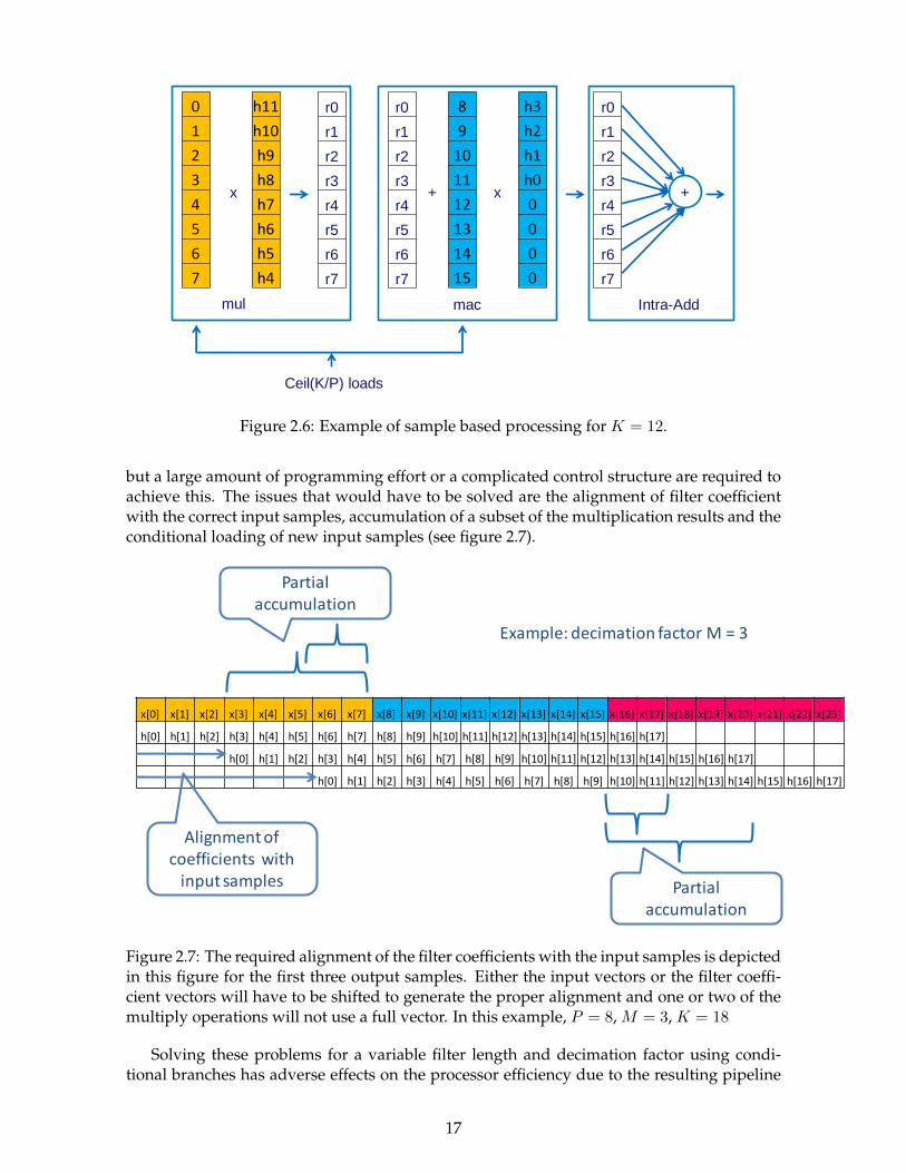
The sample based method distributes the multiplications in the different filter taps over theslices the SIMD processor. This corresponds to the parallelization of the elements in the sumof equation 2.4.
The sample based approach requires input vectors that are aligned at multiples of thedecimation factor. The amount of vector loads required for each output sample is dK/P e(see figure 2.6. When symmetry in the filter is not exploited, dK/P e vector multiplications(and dK/P e − 1 accumulations) are needed. An extra step is required to sum all multiplica-tion results into one output sample, which reduces a vector to a scalar value. This is calledan Intra-Vector Addition (IVA) in the EVP instruction set. We assume that the result of thisreduction is stored in an accumulation vector which buffers P output samples before initiat-ing a store operation. The coefficients of the filter are assumed to be loaded into one or morevector registers only once for all output samples, so these load operations are ignored in thisanalysis. The total amount of instructions required for the production of one output sampleis given by: ⌈
K
P
⌉LOAD +
⌈K
P
⌉MAC + 1 IV A+
1
PSTORE (2.8)
It is apparent that the utilization of the processor depends on the number of filter coeffi-cients. If K is not a multiple of P , then there will be a MAC instruction which does not useall processing elements.
The distance between the first sample used for the production of output m and outputm + 1 is M samples. This means there is an overlap of K − M samples in the involvedcalculations. A naive implementation would use K
M times more memory bandwidth per out-put sample than strictly required. Loading the same data twice should therefor be avoided,
16
0
1
2
3
4
5
6
7
8
9
10
11
12
13
14
15
h11
h10
h9
h8
h7
h6
h5
h4
x +
h3
h2
h1
h0
0
0
0
0
x
r0
r1
r2
r3
r4
r5
r6
r7
mul mac
r0
r1
r2
r3
r4
r5
r6
r7
r0
r1
r2
r3
r4
r5
r6
r7
+
Intra-Add
Ceil(K/P) loads
Figure 2.6: Example of sample based processing for K = 12.
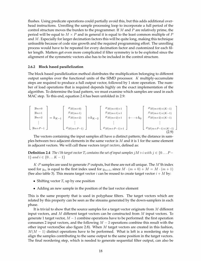
but a large amount of programming effort or a complicated control structure are required toachieve this. The issues that would have to be solved are the alignment of filter coefficientwith the correct input samples, accumulation of a subset of the multiplication results and theconditional loading of new input samples (see figure 2.7).
x[0] x[1] x[2] x[3] x[4] x[5] x[6] x[7] x[8] x[9] x[10] x[11] x[12] x[13] x[14] x[15] x[16] x[17] x[18] x[19] x[20] x[21] x[22] x[23]
h[0] h[1] h[2] h[3] h[4] h[5] h[6] h[7] h[8] h[9] h[10] h[11] h[12] h[13] h[14] h[15] h[16] h[17]
h[0] h[1] h[2] h[3] h[4] h[5] h[6] h[7] h[8] h[9] h[10] h[11] h[12] h[13] h[14] h[15] h[16] h[17]
h[0] h[1] h[2] h[3] h[4] h[5] h[6] h[7] h[8] h[9] h[10] h[11] h[12] h[13] h[14] h[15] h[16] h[17]
Alignment of coefficients with
input samples Partial accumulation
Partial accumulation
Example: decimation factor M = 3
Figure 2.7: The required alignment of the filter coefficients with the input samples is depictedin this figure for the first three output samples. Either the input vectors or the filter coeffi-cient vectors will have to be shifted to generate the proper alignment and one or two of themultiply operations will not use a full vector. In this example, P = 8, M = 3, K = 18
Solving these problems for a variable filter length and decimation factor using condi-tional branches has adverse effects on the processor efficiency due to the resulting pipeline
17
flushes. Using predicate operations could partially avoid this, but this adds additional over-head instructions. Unrolling the sample processing loop to incorporate a full period of thecontrol structure moves the burden to the programmer. If M and P are relatively prime, theperiod will be equal to M × P and in general it is equal to the least common multiple of PandM . Especially for larger decimation factors this will be quite long, making this techniqueunfeasible because of code size growth and the required programming effort. The unrollingprocess would have to be repeated for every decimation factor and customized for each fil-ter length. Matters get even more complicated if filter symmetry is to be exploited since thealignment of the symmetric vectors also has to be included in the control structure.
2.6.2 Block based parallelization
The block based parallelization method distributes the multiplication belonging to differentoutput samples over the functional units of the SIMD processor. K multiply-accumulatesteps are required to produce a full output vector, followed by 1 store operation. The num-ber of load operations that is required depends highly on the exact implementation of thealgorithm. To determine the load pattern, we must examine which samples are used in eachMAC step. To this end, equation 2.4 has been unfolded in 2.9:
ym+0
ym+1
ym+2...
ym+P−1
= hK−1
xM(m+0)
xM(m+1)
xM(m+2)...
xM(m+P−1)
+hK−2
xM(m+0)+1
xM(m+1)+1
xM(m+2)+1...
xM(m+P−1)+1
+· · ·+h0
xM(m+0)+(K−1)xM(m+1)+(K−1)xM(m+2)+(K−1)
...xM(m+P−1)+(K−1)
(2.9)
The vectors containing the input samples all have a distinct pattern; the distance in sam-ples between two adjacent elements in the same vector is M and it is 1 for the same elementin adjacent vectors. We will call these vectors target vectors, defined as:
Definition 2.4 The i’th target vector Ti contains the set of input samples jM+i with j ∈ {0 . . . P−1} and i ∈ {0 . . .K − 1}
K ·P samples are used to generate P outputs, but these are not all unique. TheM ’th indexused for ym is equal to the first index used for ym+1, since M · (m + 0) +M = M · (m + 1)(See also table 3). This means target vector i can be reused to create target vector i+M by:
• Shifting vector Ti up by one position
• Adding an new sample in the position of the last vector element
This is the same property that is used in polyphase filters. The target vectors which arerelated by this property can be seen as the streams generated by the down-samplers in eachphase.
It is trivial to show that the source samples for a target vector originate from M differentinput vectors, and M different target vectors can be constructed from M input vectors. Togenerate 1 target vector, M − 1 combine operations have to be performed: the first operationconsumes 2 input vectors, and the following M − 2 operations combine this result with theother input vectors(See also figure 2.8). When M target vectors are created in this fashion,M(M − 1) distinct operations have to be performed. What is left is a reordering step toalign the samples contributing to the same output to the same position in the target vectors.The final reordering step, which is needed to generate sequential filter output, can also be
18

Target vector: 0 1 2 3 4 5 6 7 8y0 0 1 2 3 4 5 6 7 8y1 3 4 5 6 7 8 9 10 11y2 6 7 8 9 10 11 12 13 14y3 9 10 11 12 13 14 15 16 17y4 12 13 14 15 16 17 18 19 20y5 15 16 17 18 19 20 21 22 23y6 18 19 20 21 22 23 24 25 26y7 21 22 23 24 25 26 27 28 29
Table 3: Example of the input sample indexes used in the first 9 target vectors for M = 3 andP = 8.
Combine
8
9
10
11
12
13
14
15
0
1
2
3
4
5
6
7
+
0
9
X
3
12
X
6
15
16
17
18
19
20
21
22
23
+
0
9
18
3
12
21
6
15
0
3
6
9
12
15
18
21
Combine Reorder
0
9
X
3
12
X
6
15
0
9
18
3
12
21
6
15
Figure 2.8: Construction of a target vector for M = 3
incorporated here, bringing the total amount of reordering steps to M. The total amount ofinstructions required to generate M target vectors in the correct order is M2.
Using the first M target vectors, all other target vectors required for one output vectorcan be generated using the shift and add strategy. The full algorithm for the decimating filteroperation is show in algorithm listing 1.
Algorithm 1 Block based decimating filterwhile Input samples are available do
Generate M target vectors, combine and reorder using M2 instructionsfor i = 0 to K − 1 do
Perform a MAC step using target vector Ti mod MLoad a new sample from the memoryUpdate Ti mod M with this sample
end forSave output vector
end while
A few remarks can be made about this algorithm. First of all, the register pressure in-creases as the decimation factor increases. M target vectors have to be stored at any giventime. There are alsoM different masks and shuffle patterns associated with the combine andreorder actions needed to generate the first target vectors.
Secondly, filter symmetry cannot be exploited. The two symmetric target vectors are
19

not available at the same time in the general case. A variation on the algorithm could becreated, where 2 blocks of M target vectors are created, at the opposite ends of the filterwindow. However, this would double the cost for the combine and reorder stage in terms ofthe number of required instructions. Twice as many target vectors would have to be created,increasing the register pressure (although the masks and shuffle patterns can be reused).
We can conclude that the block based algorithm can be applied to vector processors witha random vector length without loss of efficiency. However, a significant portion of the timeis spent creating the required target vectors. This is the problem that we will try to solve insection 3.
2.6.3 Matrix transpose
Block based processing can be applied with a decimation factor M = P . If the input vectorsof the decimator are regarded as the rows of a P × P matrix, then the resulting target vec-tors are equal to the rows of the transposed version of that matrix. Matrix transpositions ofarbitrary size can be partitioned into smaller sections using the Eklundh [23] or PRIM [24]algorithms. In both algorithms, a number of transposition operations has to be performedon these partitions in order to generate the complete transposed matrix. An SIMD imple-mentation of decimation could be applied to perform matrix transpose operations, wrappedby one of these algorithms if necessary.
20

3 Proposed solution structure
3.1 Specification of goals
In the previous section we have shown there is a significant amount of effort involved whena decimation algorithm is performed on an SIMD machine. Decimation contains a largeamount of data locality when sample based parallelism is exploited, but the fixed vectorlength of the processor is not necessary a good match to the amount of filter coefficients,leading to an inefficient solution. Block based parallelization solves this problem, but trans-forms the data locality to a different form which cannot easily be exploited. A relatively largeamount of storage space is required, especially when filter symmetry is to be exploited. Thesamples that have to be combined into one vector are more than one vector length away,which implies that some form of local storage in the processor core is unavoidable.
Memory accesses are considered expensive in terms of power and latency, so loading thesame data twice from the memory should be avoided. Our solution should thus support thedata reuse as described in section 2.6.2.
If we assume that an efficient solution exists for the generation of the target vectors, thenideally, the MAC units inside the processor should form the bottleneck of the algorithm. Ifthis is the case, then the only way to increase the throughput is to add extra hardware in themain datapath. We will not consider that as part of our design space, so we will attempt tofind a solution which performs one MAC operation per cycle.
For symmetric filters, it should be possible to process two filter coefficients per cycle. Thisimplies that the bandwidth of the target vector generator has to be twice as high as the MACbandwidth. To fully exploit the available VLIW parallelism, the generation of new targetvectors should happen in parallel with the MAC operations.
The proposal that we will describe in the following sections achieves these goals by in-troducing a register file that supports write and read patterns aimed at generating the dec-imated target vectors. The write patterns store samples in the register file in a column wisefashion, in multiple columns at once. The read patterns load one sample from each column,using a strided indexed access mode. To enable the data reuse, extra columns are added,making the register file wider than the default vector width. Starting from section 3.3, eachof these aspects will be discussed in detail.
3.2 Related work
Special purpose register files aimed at the efficient calculation of 2D algorithms have beenan active topic of research. In [25] a vector register file with a transposed access mode isintroduced. Each column in the register file can be accessed in addition to the row wise accessmode available in a regular register file. This special access mode is only made available forwrites, motivated by the notion that there are usually less write ports than read ports. Thetarget application is matrix transposition, which can be performed in linear time.
A similar proposal is made in [26], where writes to the register file can be directed to boththe columns and rows of a register file.
In [27], a vector register file with diagonal registers is proposed to accelerate matrix trans-pose operations. Two new access modes are added to a regular vector register file to enableread and write operations in a diagonal direction. Two linear-time matrix transpose algo-rithms are derived using the diagonal registers. The first algorithm works in-place on amatrix that has already been loaded in the register file, while the second also includes load-store patterns. To maximize the throughput, 2 versions of the load-store algorithm are de-rived, which can be used in an alternating manner. Each store operation of the first algorithmcorresponds to a load operation to the same vector location of the second algorithm, which
21

enables the possibility to pipeline the load and store operations for different iterations. Theextra access modes are implemented by adding extra read, write and select lines to each bit-cell in the register file. Both [25] and [27] are aimed at accelerating matrix transposition andthere is no support for other decimation factors.
[28] introduces a stream register file with indexed access. This work is aimed at a streamprocessors, but the authors assume that similar techniques could be applied to vector pro-cessors as well.
The basic idea proposed in this paper is to break the sequential data access restrictionthat is present in stream processors. Explicitly indexed access to the register file is allowed instead of loading consecutive data samples. The register file is assumed to be implemented asan SRAM. The subdivision of an SRAM into smaller memory arrays is exploited to supportthe indexed accesses. An SRAM consists of a number of banks, which are each divided intoa number of sub-arrays. Each sub array of each bank can be addressed differently in theproposed implementation. This comes at the expense of extra address decoders for eachsub-array.
Loading two samples from the same sub-array in the same cycle is not possible, which iswhy an arbiter for distribution of the memory resource to different consumer streams is in-troduced. FIFOs are used to buffer the request addresses and resulting data samples. Whena resource conflict occurs between two streams, one of the two FIFOs is stalled. This impliesthat the latency of a read operation is non-deterministic, and may lead to processor stallswhen a data access is attempted before the read completes. If the access patterns are knownat compile-time, these conflicts can be analyzed and exact access times can be derived, butfor data-dependent access patterns the worst-case delay always has to be assumed. Commu-nication between different banks is required to allow access to all registers from each streamprocessor.
The proposed register file architecture could be used to support decimation on a vectorprocessor, although there would still be a significant overhead involved in reordering theretrieved data samples to generate the target vectors that are required for the block basedparallelization. To see what causes this overhead, we assume each vector element is storedin a separate sub-array and there is one bank. When a set of vectors has been stored in-orderin the memory, then there is no guarantee that all elements of a target vector are stored indifferent sub-arrays. These conflicts have to be resolved by the arbiter, introducing stalls.The samples that are loaded from the same sub-arrays have to be transported to differentvector slots and the overall order of the retrieved samples has to be changed to group thecalculations belonging to the same output sample on the same processing element. Whenthis register file is applied to a vector processor, the combination of the FIFO system, arbiterand inter-sample reordering require the same functionality as a full crossbar. Our proposedsolution divides the reordering of the input samples into a write and a read stage, whichleads to a more hardware efficient solution.
3.3 Rotator approach
In this section we will start by describing an intuitive implementation of a decimation algo-rithm using a decimating register file (DRF). In section 3.4 this algorithm will be adapted toreduce the hardware cost.
Several of the steps that are taken are illustrated with examples. In these examples, wewill depict the vector elements as blocks in a column. The background color denotes thesource vector of the element. The number in the cell denotes the sample number. The registerfile itself will be depicted as a grid of height P .
We will assume that the input of our register file comes from the memory and is ordered
22

sequentially. For a decimation factor M , M load operations are required to build the first Mtarget vectors. This corresponds to M write operations to the register file. In figure 3.1 this isillustrated for M = 3. Vectors can only be written columns wise and the samples retain theirorder in this direction. This is the first opportunity in which data locality is exploited.
0 3 6
1 4 7
2 5
16
17
18
19
20
21
22
23 Example: decimation factor M = 3
Input vectors
0 3 6 9 12 15
1 4 7 10 13
2 5 8 11 14
0 3 6 9 12 15 18 21
1 4 7 10 13 16 19 22
2 5 8 11 14 17 20 23
Target vectors:
8
9
10
11
12
13
14
15
0
1
2
3
4
5
6
7
Figure 3.1: The three input vectors in this example are used to generate the first target vectorsfor a decimation factor M = 3.
Two general sample movement types can be observed:
• A vertical alignment at multiples of the decimation factor
• A spreading of the input vector over multiple columns
3.3.1 Vertical alignment
The vertical alignment corresponds to a rotation operation, where each consecutive columnis rotated by M with respect to the previous column. This is illustrated in figure 3.2. Oneimportant observation that can be made is that the direction of the rotation can be either upor down. This eliminates the possibility to implement the rotation as a uni-directional shifter,which would have required a smaller amount of hardware. Formally, we will define rotationas:
Definition 3.1 A rotation over distance i of vector V , denoted as rot(V, i), is defined as:
Vo = rot(V, i) := Vo[j] = V [mod(j + i, P )] with j ∈ 0, 1, ..P − 1 (3.10)
Because the modulo operator is poorly defined for negative dividends, we will definethis case explicitly:
mod(a, n) = n−mod(|a|, n) with a ∈ Z− (3.11)
By this definition, input vectors wrap around when rotated across the boundary of theregister file. Figure 3.3 shows what content of the register looks like in this implementation.
The rotation that has to be applied to a column can be split into two components: anoffset that is applied to the first column in which the current input vector is written, and arelative displacement with respect to that column, depending on the relative distance. Wewill call the number of the first column in which an input vector j is written sj , starting at 0
23

M = 3
Target vectors:0
1
2
3
4
5
6
7
0
1
2
3
4
5
6
7
0
1
2
3
4
5
6
7
8
9
10
11
12
13
14
15
8
9
10
11
12
13
14
15
8
9
10
11
12
13
14
15
16
17
18
19
20
21
22
23
8
9
10
11
12
13
14
15
16
17
18
19
20
21
22
23
16
17
18
19
20
21
22
23
Rotation by M:
Rotation by 2M:
Rotation to other direction
required, eliminates possible
implementation with shifters
Figure 3.2: Three target vectors, constructed as the rotation and combination of three inputvectors. The rotation is bi-directional.
0 3 6 9 12 15 18 21
1 4 7 10 13 16 19 22
2 5 8 11 14 17 20 23
3 6 9 12 15 18 21 16
4 7 10 13 8 19 22 17
5 0 11 14 9 20 23 18
6 1 12 15 10 21 16 19
7 2 13 8 11 22 17 20
Figure 3.3: The three target vectors in rotated and wrapped form. A write enable mask hasto be used in the columns marked by the white boxes to prevent old samples from beingoverwritten.
for the most left column. An rotation oj is applied to this column. The rotation oi that has tobe applied to column i can then be described as:
oi = mod(oj +M · (i− j), P ) with i ≥ j (3.12)
24

The offset oj can be expressed as a function of the number of input vectors which hasbeen inserted into the register file. For input vector j, oj is given by:
oj = −mod(j ·mod(P,M),M) (3.13)
The number of the first column to which should be written, sj , is also a function of thenumber of the input vector. For input vector j, sj is given by:
sj =
⌊P · jM
⌋(3.14)
In figure 3.3, the white boxes highlight 2 columns in which samples originate from twodifferent input vectors. If we assume that the input vectors are written sequentially, thenmeasures will have to be taken to make sure that samples that have been written to theregister file in a previous cycle are not overwritten. This is why we introduce write masksfor each column. Such a mask consists of a series of P boolean values and acts as a writeenable signal for a cell in the register file. We will call the write mask of column i wmi. Thevalue of the boolean used at row r is defined as a function of the column number and oj :
wmi[r] =
1 if i 6= sj1 if i = sj and r ≥ |oj |0 if i = sj and r < |oj |
(3.15)
3.3.2 Horizontal spreading
The number of columns to which an input vector has to be written depends on the vectorlength P and the decimation factor M . If M is guaranteed to be larger than 1, then a maxi-mum of 0.5P columns are (partially) filled with samples from one input vector. This impliesthere is a maximum of 0.5P different rotated versions that have to be created. To save hard-ware resources, two columns can share one rotator, as long as they are separated by at least0.5P−1 columns. A column enable signal is added in addition to the write masks introducedin the previous section. A bitwise ’and’ operation of these two signals determines if a cell iswrite enabled in a certain cycle. To decrease the controller complexity, we will always write0.5P columns when a write instruction is executed, even though this is not always necessary.The extra columns to which is written will be filled with useful data in later iterations.
3.3.3 Evaluation
The approach which has been described in the this section contains all the ingredients thatare needed to generate the target vectors that are required by the block based decimationalgorithm. However, there are some disadvantages involved with the number of requiredrotators. Since there is a lot of sample transport involved, it is a very wire intensive solution,which requires a large amount of area. The generation of the target vector is complete afterthe write stage, which leads to complicated write logic and simple read logic. During theread phase, a row can be selected from the register file and each column forwards a cell fromthat row to an output bus.
In section 3.4 we will show that moving part of the complexity from the write stage tothe read stage results in a more hardware efficient and versatile design.
3.4 Rotatorless approach
The read logic introduced in the previous section contains a simple row decoder of whichthe output can be shared by all columns, since the same cell is returned from each column. If
25

8
9
10
11
12
13
14
15
0 8 16
1 9 17
2 10 18
3 11 19
4 12 20
5 13 21
6 14 22
7 15 23
0
1
2
3
4
5
6
7
16
17
18
19
20
21
22
23
M = 3
PMasked
write
0
1
2
3
4
5
6
7
Figure 3.4: Example of the masked write approach for M = 3. The three input vectors arewritten to the register file using masked writes. The vertical position of the samples does notchange and spreading is performed in the horizontal direction.
it were possible to select a different cell in each column, then the functionality provided bythe rotators in the write phase can be substituted by an address generator in the read phase.In stead of performing the vertical alignment by storing rotated input vectors, it could bedone by the indexed addressing of cells in each column. This idea is illustrated in figure 3.4.In the following sections we will discuss the details of the implementation.
3.4.1 Horizontal spreading and masked writing
The rotators which were present in the previous solution have been replaced by a set of maskgenerators. These mask generators enable the storage of different pipeline stages, which willbe discussed in detail in section 3.4.5. The masks are used to write a subset of the samplesfrom an input vector to each column. They eliminate all redundancy in the register file byonly storing each sample once. The masks themselves can be generated by rotating a singlebase mask, consisting of M ones, followed by P −M zeros. Since each mask consists of onlyP bits, this forms a great simplification compared to the rotators which were used on inputvectors in the previous approach.
The masks rotation that corresponds to each column can be calculated in a similar wayas the rotation of the input vectors; a simple sign switch of the rotation oi is sufficient:
oi = −mod(oj +M · (i− j), P ) with i ≥ j (3.16)
The mask that was introduced in the previous section to prevent samples from previousiterations to be overwritten, can also still be applied. A bitwise ’and’ operation of this maskand the non-rotated base mask generates exactly the mask shape that is required. The resultcan then be rotated according to equation 3.16 and used for column sj .
3.4.2 Indexed reading
During the read phase, the samples corresponding to a single target vector have to be ex-tracted from the register file. To reach this goal, an address generator is used to calculate theindexes of the samples that should be loaded from each column. This address generator hastwo parameters:
26

• A virtual row identifier (r)
• A stride (str), which for decimation functionality is equal to the decimation factor. Thestride is the relative increase of the row index between two adjacent columns.
The index idx for column i corresponding to virtual row r, can be calculated as:
idxi = mod(r + i · str, P ) (3.17)
If the stride is chosen to be equal to the decimation factor that was used during the writephase, then the output corresponding to virtual row r is equal to the output which wouldhave been returned in the rotator approach proposed in section 3.3 for row r.
3.4.3 Extra Columns
3 6 9 12 15 18 21 24
4 7 10 13 16 19 22 25
5 8 11 14 17 20 23 26
6 9 12 15 18 21 24 27
7 10 13 16 19 22 25 28
8 11 14 17 20 23 26 29
0 3 6 9 12 15 18 21
1 4 7 10 13 16 19 22
2 5 8 11 14 17 20 23
P
Figure 3.5: This figure illustrates the redundancy that is present in the register file when 9individual target vectors are stored in different rows forM = 3. AfterM rows, the content ofP − 1 columns can be reused. (In this figure and in figure 3.6, the virtual rows are drawn, tokeep these images simple. The real samples are still stored according to the patterns definedin section 3.4)
Up until now, we have depicted the register file as a grid of P × P cells. If we woulduse such a grid to store all the required target vectors, we would need P ×K word cells tostore K target vectors. This situation is depicted in figure 3.5. As previously noted, thereis a lot of redundancy present inside the register file in this case, because P − 1 columnsare reused after M rows. To remove this redundancy, a set of extra columns is added to theregister file. These columns can be used to store one or more additional input vectors whichwould sequentially follow the M input vectors which are stored in the first P columns. Eachcolumn which is added creates the potential to extract M additional target vectors from theregister file (see figure 3.6).
We will call the number of extra columns E. The total number of columns in the registerfile is equal to P +E. To select the target vectors which are partially stored in theE-columns,
27

0 3 6 9 12 15 18 21 24 27
1 4 7 10 13 16 19 22 25 28
2 5 8 11 14 17 20 23 26 29
P E
Figure 3.6: The content of the register file using extra columns. All the duplicate sampleswhich were present in figure 3.5 are removed.
a column offset parameter (coff ) is added to the read port of the register file. The offsetrequired to select target vector Ti from the register file is equal to:
coff =
⌊i
M
⌋(3.18)
The virtual row which should be activated to select Ti is equal to:
ri = mod(i,M) (3.19)
3.4.4 Read ports
To be able to perform one MAC operation per cycle, the target vector generator has to havea bandwidth which is twice as high as the MAC bandwidth. To meet this requirement,two read ports have to be attached to the decimating register file. As a consequence, twoaddress generators have to be included in the design. These read ports can be used to retrievesymmetric vector pairs and forward these to the ALU. The ALU can then execute an addoperation, which is followed by a MAC.
3.4.5 Stage Rotator
Loads from the background memory have a high latency. During the time between the ex-ecution of the load and the moment at which the data is available, other (independent) in-structions can be scheduled. For small loop kernels, these instructions can be generatedusing software pipelining.
If we want to combine software pipelining with the decimating register file, then it mustbe possible perform a read from the register file in parallel with a write belonging to a differ-ent software pipeline stage. These write operations may not overwrite data which still hasto be read in the upcoming cycles, so the data has to be stored in a separate location in theregister file. By doing so, multiple stages are present in subsequent rows of the virtual view.
To make this possible, a stage rotator is introduced. The stage rotator takes the input vectorand is able to align it by rotation, in such a way that no old data is overwritten when it isstored in the register file. The write masks have to be rotated by the same distance (see alsofigure 3.7). This extra rotation can be added to the offset oj , which represented the rotationdistance for the first column in which samples should be written for input vector j. The extrarotation is called stagerot and it is added to the dividend of the modulo operation. With thisextension, the equation describing oj becomes:
oj = −mod(mod(j ·mod(P,M),M) + stagerot, P ) (3.20)
28

M = 3
P
32
33
34
35
36
37
38
39
24
25
26
27
28
29
30
31
Masked
write
37
38
39
32
33
34
35
36
29
30
31
24
25
26
27
28
Rotation
0 29 8 37 16
1 30 9 38 17
2 31 10 39 18
24 3 32 11 19
25 4 33 12 20
26 5 34 13 21
27 6 35 14 22
28 7 36 15 23
Figure 3.7: Example of the usage of the stage rotator for M = 3. The yellow and green inputvector are rotated and subsequently written to the register. The columns to which they arewritten are the same as those that were used in the previous stage. The write masks havebeen rotated by the same amount as the input vectors.
This implements a form of double buffering, and it can be used for decimation factors up toand including 0.5P . For higher decimation factors there aren’t enough virtual rows in theregister file to store two blocks of M rows.
As a general rule, stagerot has to increase by M after each stage and may wrap aroundwhen the bottom of the register file is reached.
3.5 Parameter determination
There are three design parameters that determine the proportions of the proposed solution:the number of processing element P , the number of extra columns E and the word width ofeach processing element, which we will call W . If we start with the template sketched by theEVP, then the product of P and W is fixed at 256 bits, and possible values for W are 8, 16 or32 bits.
3.5.1 Effects of parameter P
The parameter P is equal to the maximum decimation factor which can be supported effi-ciently by the register file. As noted in the previous section, 0.5P is the maximum decimationfactor which can be used in a pipelined operation mode.
P also determines the storage capacity of the register file, although the other parametersalso contribute. There are P + E columns, each containing P words of W bits. The totalcapacity in bits is equal to:
Capacity =W · P · (P + E) bits (3.21)
The ability to switch to different word widths should also be taken into account when se-lecting a value for P andW . A view switch from a lower word width to a higher word widthis possible with some minor adaptation to the controller. For example, two 16 bit words canbe combined to form one 32 bit word. An example for P = 16 and M = 3 is shown in figure3.8. The upper half of each word is stored in the even columns, while the lower half is storedin the odd columns. It is essential to store the lower and upper half in different columns,because they have to be read simultaneously.
29

0 1 2 3 4 5 6 7 8 9 10 11 12 13 14 15 16e17e18e19e0 0 8 16 241 0 8 16 242 1 9 17 253 1 9 17 254 2 10 18 265 2 10 18 266 3 11 19 277 3 11 19 278 4 12 20 289 4 12 20 2810 5 13 21 2911 5 13 21 2912 6 14 2213 6 14 2214 7 15 2315 7 15 23
Figure 3.8: This figure illustrates a view switch, using a register file designed for W = 16 tostore 32 bit words.
To support this write pattern the mask generators have to be extended slightly with analternative operation mode in which the M ones in the base mask are stored in the first Meven positions of the mask. The relative mask rotation of the odd columns with respect tothe previous column is fixed at 1. The read address generators of the odd rows also requireslightly different behaviour. Equivalent to the change that was made to the mask rotators,the indexes of the odd columns need a fixed difference of 1 compared to the previous evencolumn.
A switch from a high word width to a lower word width is not possible without signif-icant changes to the hardware. Since there are not enough columns to store each half-wordin a separate column, columns would have to be shared. The mask generators would haveto work at the granularity of half words and non-consecutive half words would have to beselectable from the same column. The costs of these changes are the reason this is not con-sidered as a realistic option.
Designing the register file for the lowest possible word width would allow scaling toall higher word widths. However, this is also the most hardware intensive design, sincethe size of the register file scales with P 2. The rotators and mask generators also work atthe granularity of the smallest word width, so they too scale upwards when P is increased.A trade-off between the hardware size and the required flexibility should be made whenchoosing the value of parameter P .
3.5.2 Effects of parameter E
The number of extra columnsE determines the amount of target vectors that can be extractedfrom the register file. This number should at least be equal to the number of filter coefficients.The first block of P columns holds M potential target vectors. For each extra column whichis added, M more target vectors can be generated. If K target vectors have to be extracted
30

E Max. order Max. K0 1 M1 2 2M2 3 3M3 4 4M4 5 5M5 6 6M
Table 4: Maximum filter order and the maximum number of filter coefficients as a functionof E for Mmax ∈ {8, 16, 32}
from the register file, E should be at least equal to:
E ≥⌈K
M
⌉− 1 (3.22)
If we combine equation 3.22 with equation 2.7, we can determine the value of parameter Ebased on the maximum sinc filter order we would like to support, given the fact that M isbounded between 2 and P . For Mmax ∈ {8, 16, 32}, the maximum sinc filter order which canbe supported at different values for E are enumerated in table 4.
Some remarks can be made about these numbers. First of all, for small decimation fac-tors, more than one block of M rows can fit in the register file. Higher order filters can besupported by using multiple blocks for a single output vector. The second thing that shouldbe taken into consideration is the effect of a view switch to a higher word width on the num-ber of extra columns. If the word width doubles, the number of extra rows is effectivelydivided by two. If such view switches are to be supported, the number of extra rows shouldbe even, or else an unusable column will be created when the view switch is activated.
3.6 Programming rules and interface
In the previous sections we have described the functionality of all the parts which make upthe DRF. In the following two sections we will make the translation to the interface that willbe exposed to the programmer.
3.6.1 Programming interface
Two basic primitives have to be provided to the programmer to enable interaction with theregister file: a read command and a write command.
For a write command, the following parameters are required by the register file:
• The decimation factor M
• The vector length P
• The current stage, stored in stagerot
• The number of the input vector j
• The input vector
Providing all these parameters for each write command is unnecessary, since the majoritydoes not change between consecutive writes. That is why the controller of the register filecontains a set of state variables which only have to be initialized once for a series of writeoperations. These initialization parameters are:
31

• The decimation factor M
• mod(P,M), provided as a constant to remove the need for a hardware modulo unit
•⌊PM
⌋, provided as a constant to remove the need for a hardware division unit
• The number of vectors which will be written per stage. This is used to enable theautomatic generation of the right stagerot value. We will call this parameter nv
The exact use of each of these parameters will be discussed in section 4.4, which explains thehardware structure of the controller. When the initialization is complete, the input vector isthe only parameter that is left in the write command.
For a read command, 3 parameters are required:
• The selected virtual row r
• The stride str
• The column offset coff
Read commands which are used for a decimating filter will also follow a specific patternwhich makes them predictable. Symmetric vectors will be selected from the register file,probably in sequential order. The 3 read parameters can all be derived from knowledge of thefilter length, the decimation factor and the number of preceding read commands. Taking thisinto account creates a very simple read interface. If we assume the stride to be equal to thedecimation factor, which has been stored in the state of the controller during initialization,then there are 2 parameters left which enable the creation of a simple read command andcontroller:
• mod(K,M), needed to determine the virtual row of the last symmetric vector
•⌊KM
⌋, needed to determine the virtual column of the last symmetric vector
Two versions of the read command can be created, one for each read port.The described programming interface is summarized in table 5.
The interface that is proposed in this section is specifically tailored for decimation. Forother possible applications of this register file, a more general access method may be re-quired.
3.6.2 Programming rules
The interface that was defined in the previous section can be used to write programs usingthe DRF, but the results will only be as correct if certain rules are followed.
The register file will have to be initialized before a read or write action is allowed. Be-fore initialization, the result of a write or read is not defined. Re-initializing the register filebetween a write and read, or between consecutive reads also isn’t allowed. We will not for-mally define the output in these cases, but it is imaginable that an initialization triggers thereset of all internal counters, invalidating the state of the register file.
The write operation may not target the same stage as the two read operations which aredone in parallel. This can be understood intuitively, since the target vectors which couldpotentially be loaded from the same stage as the write operation are not complete yet.
To make the dependencies explicit for the scheduler, we choose to introduce a barrierstatement. A barrier has to be placed in a program at the location where a new pipeline
32

Programming interfaceInitialization
Name evp drf initInput parameters M , mod(P,M),
⌊PM
⌋, nv, mod(K,M),
⌊KM
⌋Return parameters none
Write commandName evp drf writeInput parameters input vectorReturn parameters none
Read commandName evp drf read0Input parameters noneReturn parameters Read port 0 outputName evp drf read1Input parameters noneReturn parameters Read port 1 output
Table 5: Programming interface
stage is started. Reads and writes in between two barrier statements are assumed to targetdifferent stages and may be reordered by the scheduler. The relative order of the writes andthe relative order of the reads still has to be respected, since each of these statements triggersa state update of the register file.
Appendix B shows a section of code using the proposed programming interface.
3.7 Extra functionality
In the previous sections we have shown how the proposed register file could be used tosupport decimation. In this section we will show other applications for which it can also beused with some small adaptations to the controller.
3.7.1 Decimation by 1
Up until now, we have only shown the behaviour of the register file for decimation factorshigher than 1. When vectors are stored using M = 1, they can be read back in exactly thesame order as they were written. The register file then acts as a regular storage device, inwhich P vectors can be stored. The vectors can only be stored at the diagonals of the registerfiles, because each element in the input vector can only be stored at one specific row, andonly one element can be selected from each column during a read (see figure 3.9). The stagerotation mechanism has to be used to place the vector at a specific virtual row.
To be able to support decimation by 1, P columns must be writable in the same cycle,while we assumed in section 3.3.2 that only 0.5P distinct (mask) rotators would be required.To generate the extra masks which are required for decimation by 1, the first 0.5P masks arerotated by 0.5P positions. This is illustrated in figure 3.10.
Possible usecases for decimation by 1 are register spilling or context save and restore.The number of accesses to the background memory could be reduced, or a higher effectivecontext store bandwidth can be achieved, by partially storing the context in the DRF.
33

0 57 50 43 36 29 22 15
8 1 58 51 44 37 30 23
16 9 2 59 52 45 38 31
24 17 10 3 60 53 46 39
32 25 18 11 4 61 54 47
40 33 26 19 12 5 62 55
48 41 34 27 20 13 6 63
56 49 42 35 28 21 14 7
Figure 3.9: The locations at which vectors are stored for M = 1
11
1
1
1
11
1
0.5P 0.5P
P
Figure 3.10: The generation of the masks for the left and right half of the DRF. Each columndenotes a write mask, and a 1 denotes a write enable.
3.7.2 Interpolation output reordering
In section A.1.1 of appendix A we introduce interpolation, the dual of decimation. We showthat a polyphase implementation of the interpolation algorithm generates a set of outputvectors that is decimated by L. The decimated vectors have to be interleaved into one outputstream. This operation can be performed efficiently using the proposed register file.
During the write phase, each sample is stored in a column exactly once as shown in figure3.11. This implies that the write mask consists of a single ’1’, and P − 1 zeros. The relativerotation of the mask that is used a in column with respect to its left neighbor is equal to −L,so the write enable moves down L locations for each column. The write mask for columnzero is rotated upwards by L after each written input vector. The first column to whichshould be written is always the 0’th column.
During the read phase, the virtual rows can be read in such an order so that sequentialoutput is read from the register file. In equation 3.14 we provided a means to determinethe first column in which should be written, based on the number of the input vectors for
34

0 1 2
3 4 5
8 6 7
9 10 11
12 13 14
16 17 15
18 19 20
21 22 23
P
L
L
0
3
6
9
12
15
18
21
1
4
7
10
13
16
19
22
2
5
8
11
14
17
20
23
Input vectors
Figure 3.11: An example of the write pattern for L = 3. One sample from each input vectoris written to each column, using a write stride of −L. The rotation of the write mask forcolumn 0 is equal to mod(j · L,P ), where j is the number of the input vector. The numbersin the vector slots denote the desired output sample index.
decimation. The same relation holds between the row that should be read, based on thenumber of the output vector. If we want to retrieve the i′th output vector, we should activaterow
ri =
⌊P · iL
⌋(3.23)
The read address generators should work based on the column number and the numberof the output vector. The index idx for column c corresponding to output vector i, can becalculated as:
idxc = mod(
⌊c+ i · P
L
⌋, P ) (3.24)
The algorithm that was described in this chapter shows great similarities with the deci-mation algorithm. The write patterns for interpolation were used for reading during deci-mation, and vice versa.
3.7.3 Exposure of the column read indexes
To efficiently support decimation we introduced an address generator to index the columnsof the register file. This address generator has an output width of (P + E) · log2P bits. Forcertain applications it might be useful to expose the column indexing to the programmer.One or several index vectors could be loaded into the register file controller through the portwhich is normally used to load input vectors. The number of index vectors that could beloaded depends on the actual dimensions of the register file, set by P and W . These indexvectors can then be used to select specific elements from each column. This can be used toemulate the behaviour of a shuffle operation, when all columns are filled with the same inputvector.
35

4 Hardware structure
This section will give a description of the hardware implementation that was made of thedecimating register file. A VHDL model was created which has been synthesised and placedby the Cadence Encounter RTL compiler. The hardware model includes all the features listedin section 3.4 and also has the ability to decimate by 1.
The controller does not support all the features which were described in section 3.6.1.The controller is not aware of the filter length, removing the functionality of automated stageswitching and symmetric vector selection. In stead, in the write stage, read row and columnoffset have to be provided as an input to the unit. View switches to higher word widths arealso not supported.
The correctness of the VHDL model has been verified by simulation. An automated testbench generator was used to simplify this process.
We will start with a top level view of the design and zoom in on the column hardwareand the controller. Area and power estimations which were generated by the placement toolare shown and possible future adjustments to the hardware will be discussed.
36

4.1 Top level
In figure 4.1 the top level diagram of the decimating register file is shown. All primary inputsare drawn, excluding those which are used during the initialization. Some of the controlwires have also been omitted from this figure for clarity, they will be shown in section 4.4.
Each write mask has been coupled to two or more columns, because the maximum amountof columns which can be written in one cycle during decimation with M ≥ 2 is 0.5P . Thebitwise ’and’ of the Column Write Enable signal and the write mask is used to enable or disablea word cell.
The stage rotator can perform a bit-wise rotation of the input vector, by multiples of theword width. A rotation of 0 means the output is equal to the input.
The address generator calculates the column indexes based on the selected row. Two sep-arate output vectors are generated, one for each read port.
The column offset muxes take the words which are returned by all the columns and selectthe proper 256 bit chunk from the bus. 1 + E possible outputs can be selected.
Decimating Register file
Wx(P+E)
Wx(P+E)
256
256
Controller
Write masks (0.5P · P)
Column Write Enable (P+E)
256Stage Rotator
Input vector (256)
Read address
generator
Col Offset (ceil(Log2 (1+E)))
(P+E) Log2P
(P+E) Log2P
Col Offset (ceil(Log2 (1+E)))
Row 1 (Log2P)
Row 0 (Log2P)
Figure 4.1: Top level view of the decimating register file. The bus labels denote the width ofthe bus in bits. An optional name is added in italic. This notation will also be used in thefollowing figures.
4.2 Column level hardware
The column hardware is shown in figure 4.2. All columns are coupled to the output of thestage rotator, so they all receive the same input vector. The write enable of each word cell inthe column can be set by the mask rotators and a one bit column enable signal can globallyenable or disable a column.
Each column has two log2P bits row select inputs, which select one out of the P wordswhich are stored in the column. The selected word is forwarded to the column offset muxeson the read port busses.
37
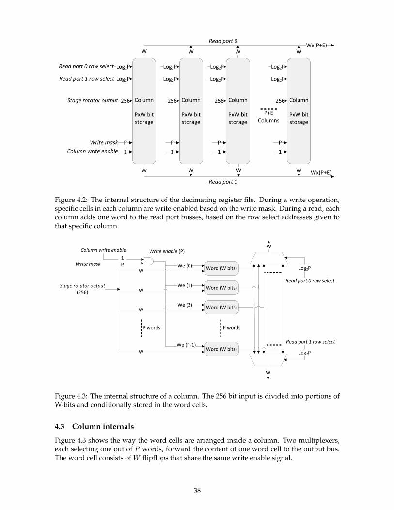
Column
PxW bit storage
Column
PxW bit storage
Column
PxW bit storage
Column
PxW bit storage
Wx(P+E)W W W
Wx(P+E)W W W
P+E Columns
256 256 256 256
P P P P
Stage rotator output
Write mask
1 1 1 1Column write enable
Read port 0 row select
Read port 1 row select
Log2P
Log2P
Log2P
Log2P
Log2P
Log2P
Log2P
Log2P
Read port 0
Read port 1
W
W
Figure 4.2: The internal structure of the decimating register file. During a write operation,specific cells in each column are write-enabled based on the write mask. During a read, eachcolumn adds one word to the read port busses, based on the row select addresses given tothat specific column.
Word (W bits)
Word (W bits)
Word (W bits)
Word (W bits)
Column write enable
Write mask
We (P-1)
Write enable (P)W
W
W
W
W
W
Stage rotator output(256)
Read port 0 row select
Read port 1 row select
P
1
We (2)
We (1)
We (0)
P words P words
Log2P
Log2P
Figure 4.3: The internal structure of a column. The 256 bit input is divided into portions ofW-bits and conditionally stored in the word cells.
4.3 Column internals
Figure 4.3 shows the way the word cells are arranged inside a column. Two multiplexers,each selecting one out of P words, forward the content of one word cell to the output bus.The word cell consists of W flipflops that share the same write enable signal.
38

4.4 Controller
MS R
PModM
PDivM
StageOffset
-
Sign Bit
-
01Cin
Shift DistanceShifter
111...11000….00
0.5P 0.5P+E
Rotation Distance
Rotate Left
Merge Mask LUT
PxP bit
Mask LUTPxP bit
Rotate Right
Rotate Left
Rotate Left
M
Rotate Left
Rotate Left
Write Masks
&M=1?
1111...111
P+E
10
Column Enable
0.5P
0.5P
Figure 4.4: Block diagram of the controller. The green area is used to generate oj , the bluearea generates sj , the yellow area generates the column enable signals and the red area isresponsible for the write masks.
The VHDL model of the DRF includes a controller which generates the indices, offsetsand masks that were described in section 3. It is by no means the most optimized controllerimaginable, but it merely shows a possible implementation. The controller is functionallycorrect and was used to test the register file through VHDL simulations. It also gives a fairrepresentation of the area that a controller for the register file would use.
A block diagram of the controller is shown in figure 4.4, to which will be referred severaltimes in this section.
The highlighted green area is responsible for the generation of the rotation offset for thefirst column, oj (equation 3.13). The combination of the two adders and the multiplexerimplements a modulo operation using an add-compare-choose circuit. The register S is ini-tialized at 0 and the update function is equal to:
Sj+1 = mod(Sj +mod(P,M),M) (4.25)
The update function is executed after an input vector has been loaded, making the content
39

of the register S at time j equal to oj . The width of register S is log2P so it wraps aroundwhen the value P is reached.
In equation 3.14, an expression is given for the number of the first column to whichshould be written. The generation of sj can be implemented using a register Rj , which isinitialized at 0. The update function adds
⌊PM
⌋to Rj for each input vector that is loaded.
Additionally, 1 can be added to Rj based on the inverted activation bit of the add-compare-choose unit. If we define C = mod(P,M), then this condition is defined as:
wrappedj =
{true if mod(j · C,M) + C 6= mod((j + 1) · C,M)false otherwise
(4.26)
Rj+1 =
Rj +⌊PM
⌋if wrappedj = false
Rj +⌊PM
⌋+1 if wrappedj = true
(4.27)
The equivalence of Rj and 3.14 has been verified by enumeration for M ∈ {0, 1, . . . P}, j ∈{0, 1, . . . 2P} and P ∈ {8, 16, 32}. The required hardware is highlighted in blue in figure 4.4.The width of register R is dlog2(P + E)e. It is not designed to wrap around and has to bereset when a new stage is started.
The yellow block is responsible for the generation of the column enable signals. It shiftsa mask of 0.5P ones by Rj positions. To support decimation by 1, it is also possible to enableall columns at once.
By addressing the Merge Mask LUT using register S, we extract the write mask for columnsj as defined in equation 3.15. This mask is rotated to incorporate the current stage offset.
The Mask LUT is indexed with M , selecting the base mask consisting of M ones andP −M zeros. This mask is used as the input for the mask generator, highlighted in orange.0.5P rotators are cascaded to implement equation 3.16. The lower log20.5P bits of Rj areused to rotate the masks to the right column position. The circuitry that is used to generatethe upper 0.5P masks for decimation by 1 is not shown. It is implemented as a multiplexernear the columns which is able to flip the lower and upper half of the received write masks,as was shown in figure 3.10.
The address generator is shown in figure 4.5. In the current implementation is is builtas a cascade of P + E − 1 wrapping adders. The stride is fixed at M , which is sufficient tosupport decimation.
StageOffset
M
P+E-1adders
To col 0
To col 1
To col 2
To col 3
To col P+E-1
Figure 4.5: The address generator
40

Identifier P W E
8x32x11 32 8 316x16x20 16 16 4
Table 6: Legend for the identifiers that are used in the synthesis and placement results
Property RemarkRotator version Uses the rotator approach (section 3.3)
Mask versionUses the rotatorless approach, i.e. only one (stage) rotation can beperformed on the input vector (section 3.4)
Output shifterImplements the column offset selection using a shifter in stead ofmultiplexer
Custom rotatorDescribes the rotators explicitly as multiplexer trees. The vhdl func-tion rotate left is not used in this case
Table 7: The table can be used in conjunction with the synthesis and placement results toidentify the hardware configuration that was used
4.5 Global placement results
Several different configurations of the register file have been implemented in VHDL, in orderto estimate the area and power costs. The differences between the versions are listed in table6 and 7.
The synthesis and placement uses a 45nm library, with a target clock frequency of 208Mhz.The resulting area is split in two partitions:
• Cell area, representing the area of the logic cells
• Net area, representing the area which is used by wiring
Several remarks can be made about figure 4.6. First of all, the rotator version is clearly largerthan the version using the write mask approach, confirming the usefulness of this adaptationto the initial design. The relative contribution of the net area also decreases slightly.
P EWW[Bits] Version
Freq.[MHz] Cell Area Net Area Total Area cell/total
Normal.area % EVP
16 4 16 Rotator version 208 67.576 68.525 136.101 0,50 100,0 7,02
16 4 16 Mask version 208 54.531 46.695 101.226 0,54 74,4 5,22
8 3 32Rotator version, Output shifter 208 35.214 33.513 68.727 0,51 50,5 3,55
8 3 32 Rotator version 208 34.725 31.662 66.387 0,52 48,8 3,43
8 3 32Rotator version, Custom rotator 208 35.847 30.352 66.199 0,54 48,6 3,42
8 3 32 Mask version 208 26.266 16.804 43.070 0,61 31,6 2,22
Figure 4.6: Placement results for different versions of the decimating register file
Two different implementations of the column offset selectors were synthesized. The firstdescription uses the VHDL function shift left on the read port busses to apply the columnoffset, while the second description explicitly implements a multiplexer. The latter approachresulted in a smaller design. A similar effect can be seen when comparing the custom rotator
41

version with the vanilla implementation. In the custom rotator version, the rotator are im-plemented as a tree of two-input multiplexers, which also resulted in a smaller design. Thisraises questions about the efficiency of the implementation of the rotate left function chosenby the synthesis tool. A possible cause for this effect could be that the tool is unable to exploitthe fact that the rotation distance is always equal to a multiple of the word width. Furtherexperiments would be required to confirm this theory, but the possible improvement whichcould be made is relatively small, especially in the write mask approach.
The last column shows the relative size of the DRF compared to an EVP synthesized withsimilar tool settings. For the P = 16 version, the best obtained result is 5.2%, for P = 8 thisis 2.2%. These numbers should be regarded as an indication of the added area, because thecost of embedding the register file in the existing EVP floor plan is not taken into account.
4.6 Area breakdown
Two of the configurations from figure 4.6 have been analyzed in more detail to determinethe relative area contribution of the components in the register file. These configurations aremarked in bold and the area breakdown is shown in figure 4.7 and 4.8.
8x32x11 version Cell Net Total % of total
Columns 21.503 11.532 33.035 76,70
Column offset muxes 2.214 1.224 3.438 7,98
Controller 712 201 913 2,12
Stage Rotator 1.609 1.535 3.144 7,30
Read addr generator 147 240 387 0,90
Decimation by 1 80 3 83 0,19
Connections 0 2.067 2.067 4,80
Others x x 3 0,01
Total 26.120 16.786 43.070 100,00
Figure 4.7: Area breakdown of the placement results for P = 8, W = 32 and E = 3. Thesyntheses was performed for a clock frequency of 208Mhz.
16x16x20 version Cell Net Total % of total
Columns 42.912 36.295 79.207 78,25
Column offset muxes 4.044 2.308 6.352 6,28
Controller 3.478 1.676 5.154 5,09
Stage Rotator 1.984 1.930 3.914 3,87
Read addr generator 700 1.185 1.885 1,86
Decimation by 1 461 225 686 0,68
Connections 0 2.947 2.947 2,91
Others x x 1.081 1,07
Total 53.579 46.566 101.226 100,00
Figure 4.8: Area breakdown of the placement results for P = 16, W = 16 and E = 4. Thesyntheses was performed for a clock frequency of 208Mhz.
The largest part of the area is taken up by the column hardware. This includes the flip-flips and the read port multiplexers, which together are responsible for over 76% of the area
42
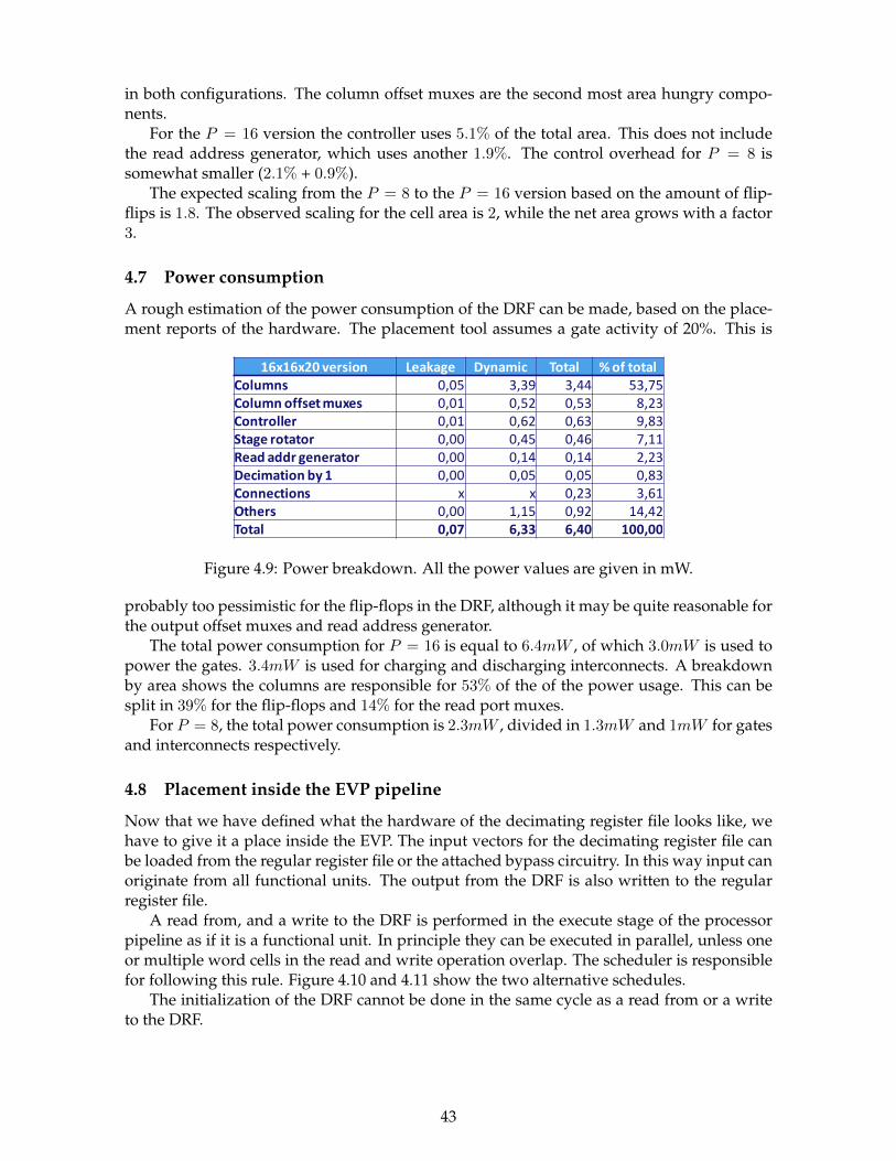
in both configurations. The column offset muxes are the second most area hungry compo-nents.
For the P = 16 version the controller uses 5.1% of the total area. This does not includethe read address generator, which uses another 1.9%. The control overhead for P = 8 issomewhat smaller (2.1% + 0.9%).
The expected scaling from the P = 8 to the P = 16 version based on the amount of flip-flips is 1.8. The observed scaling for the cell area is 2, while the net area grows with a factor3.
4.7 Power consumption
A rough estimation of the power consumption of the DRF can be made, based on the place-ment reports of the hardware. The placement tool assumes a gate activity of 20%. This is
16x16x20 version Leakage Dynamic Total % of totalColumns 0,05 3,39 3,44 53,75Column offset muxes 0,01 0,52 0,53 8,23Controller 0,01 0,62 0,63 9,83Stage rotator 0,00 0,45 0,46 7,11Read addr generator 0,00 0,14 0,14 2,23Decimation by 1 0,00 0,05 0,05 0,83Connections x x 0,23 3,61Others 0,00 1,15 0,92 14,42Total 0,07 6,33 6,40 100,00
Figure 4.9: Power breakdown. All the power values are given in mW.
probably too pessimistic for the flip-flops in the DRF, although it may be quite reasonable forthe output offset muxes and read address generator.
The total power consumption for P = 16 is equal to 6.4mW , of which 3.0mW is used topower the gates. 3.4mW is used for charging and discharging interconnects. A breakdownby area shows the columns are responsible for 53% of the of the power usage. This can besplit in 39% for the flip-flops and 14% for the read port muxes.
For P = 8, the total power consumption is 2.3mW , divided in 1.3mW and 1mW for gatesand interconnects respectively.
4.8 Placement inside the EVP pipeline
Now that we have defined what the hardware of the decimating register file looks like, wehave to give it a place inside the EVP. The input vectors for the decimating register file canbe loaded from the regular register file or the attached bypass circuitry. In this way input canoriginate from all functional units. The output from the DRF is also written to the regularregister file.
A read from, and a write to the DRF is performed in the execute stage of the processorpipeline as if it is a functional unit. In principle they can be executed in parallel, unless oneor multiple word cells in the read and write operation overlap. The scheduler is responsiblefor following this rule. Figure 4.10 and 4.11 show the two alternative schedules.
The initialization of the DRF cannot be done in the same cycle as a read from or a writeto the DRF.
43

0 1 2 3 4
drf_read0 ( stage 0 ) RRF EXE WB
drf_read1 ( stage 0 ) FETCH DEC RRF EXE WB
drf_write ( stage 1 ) RRF EXE WB
Figure 4.10: An independent write can be scheduled in parallel with two reads from thedecimating register file.
0 1 2 3 4 5 6
drf_write ( stage 0 ) FETCH DEC RRF EXE WB
drf_read0 ( stage 0 ) RRF EXE WB
drf_read1 ( stage 0 ) FETCH DEC RRF EXE WB
VALU FETCH DEC RRF EXE WB
Figure 4.11: A read from the decimating register file targeting the same stage as a writecannot be scheduled in the same cycle. This means the earliest time the result of the read isaccessible is cycle 5. The blue arrows denote the use of the bypasses.
44

5 Evaluation
In this section we will determine the expected speedup provided by the DRF if it were addedto the EVP. The comparison will be made using the block based algorithm from section 2.6.We will consider both symmetric and non-symmetric filtering.
The number of cycles that is required by the DRF solution is estimated based on thedesigned behaviour and the latency constraints set in section 4.8. The real scheduler andcompiler are not able to generate code for the DRF at this moment.
The block based decimation code for the non-DRF solution comes from the Bose firmwarelibrary for the EVP. It was used to generate a schedule for M = 3 and M = 5. The gener-ated schedule was analyzed to predict the number of cycles which would be used for otherdecimation factors.
5.1 Bose decimation
The Bose implementation follows algorithm 1. It consists of a loop which iterates over therequired number of output vectors. A poly-phase filter structure is used.
The code is setup in such a way that some freedom exists in the filter lengthK that can bechosen. K has to be a whole multiple of the decimation factor with at least two coefficientsin each phase of the filter.
The content of the loop body consists of 3 parts:
• A prologue, in which the firstM target vectors are generated. This meansM loads haveto be performed, followed by M2 combine and reorder steps, as described in section2.6.2.
• An inner loop, iterating over the filter coefficients. All M subfilters perform one MACoperation in an iteration. The loop is unrolled once and software pipelining is applied,so there are 2M MAC operations in the loop body. K
2M −1 iterations are needed for oneoutput vector.
• An epilogue, where the filter output is saved to the memory. The remaining 2M MACoperations, due to the software pipelining, also have to be executed here.
5.1.1 Schedule length
The length of the prologue schedule is determined by the load latency and the length of thereordering phase. Three cycles have to pass before the result of a load is available. The lengthof the reorder phase depends on the number of combine and reorder resources. In the EVP,there are 4 functional units that can perform combine operations:
• The Load-Store unit, which is also required for the load functionality in the prologue.
• The Shuffle unit, which is also required for the reordering
• The VMAC unit
• The VALU unit
Analytically determining the schedule length of the prologue is quite challenging due tothe resource limits and dependencies, and generating valid EVP code for a wide range ofdecimation factors would be very time consuming. To solve this problem, a small C-programwas written to generate the schedules for different values of M .
45

M 2 3 4 5 6 7 8 9 10 11 12 13 14 15 16Prologue 8 10 12 15 17 21 25 30 35 42 47 53 60 70 77Epilogue 6 5 10 7 14 9 18 11 22 13 26 15 30 17 34
Table 8: Schedule length for the Bose decimator. The cost of the inner loop is equal to 1.5K−3M for all decimation factors.
The schedule length of the inner loop is limited by the broadcast resource which is usedfor scalar to vector expansion. The broadcast resource can generate 1 coefficient double vec-tor in a cycle, and it is used for one cycle in the shift and add operation. M coefficient doublevectors have to be generated and 2M shift and add operations have to be performed. In eachinteraction, 2M MAC operations are performed, so the required amount of cycles for theloop is: 3M ·
(K2M − 1
)= 1.5K − 3M .
The epilogue schedule length is at least equal to 2M , since 2M VMAC operations areleft due to software pipelining. The MAC operation has a latency of one cycle before theresult is available outside the VMAC unit. This means one extra cycle is needed after thefinal MAC, before the store operation can be scheduled. The length of the epilogue scheduleis thus equal to 2M + 2. In table 8 the schedule lengths for M ∈ {2, 3, . . . 16} are shown. Ifthe number of filter coefficients per phase is odd, we will assume the epilogue has a lengthof M + 2. The total number of cycles required for one output vector is then equal to:
nCyclesbose = prologue+ 1.5K − 3M + epilogue (5.28)
The schedule lengths that were derived are lower limits, based on the available resourcesand dependencies. Factors that might add more cycles to the schedule are the loading ofthe combine masks and reorder patterns and the associated spilling for higher decimationfactors.
5.1.2 Symmetric filters
In section 2.6.2 we proposed an adaptation to the block based algorithm to support filtersymmetry exploitation. The analysis from the previous paragraph has to be adapted slightlyto incorporate this difference.
Two blocks of M vectors would have to be generated in the prologue which we willassume to grow by 50%. The 2 blocks of M vectors have to be updated in the inner loop,requiring 2M cycles. M coefficients have to be loaded from the memory, which can be donein 0.5M cycles. The amount of cycles spent in the loop is 2.5M( K2M − 1) = 1.25K − 2.5M . Soeven though the number of MAC operations has been reduced by a factor two, the criticalloop is only 1.5−1.25
1.5 = 17% shorter in the limit case, because we are limited by the broadcastunit. If this resource limitation would be resolved by adding a second broadcast unit, thenthe scalar load store unit would become the new bottleneck. The prologue length is reducedto M + 2 cycles, based on the M mac operations that have to be performed.
5.2 DRF decimation
The principle behind the decimation algorithm used in the Bose code is largely reused in theDRF version. The DRF version contains a main loop in which:
• New input vectors are loaded from the memory by the VLSU
• Input vectors are written to the DRF
46

• Pairs of symmetric vectors are read from the DRF
• Symmetric vectors are added by the VALU unit
• Filter coefficients are loaded from the memory using the scalar load store unit, andbroadcasted to vector size
• The VALU result is multiplied with a filter coefficient by the VMAC unit
In principle, these operations can all be done in parallel, as long as sufficient software pipelin-ing is used. One additional cycle is required to save the output vector to the memory.
There are two possible groups of functional units that may determine the schedule length.The first group consists of the VLSU resources. The amount of samples that has to be loadedfrom the memory determines the number of vector loads. The first output is a function of Kinput samples. The next output uses the same input samples, minus the M oldest samplesand adding M new samples. To generate a block of P output vectors, the number of loadsthat has to be performed is equal to:
nLoads =
⌈K + (P − 1)M
P
⌉(5.29)
We have to add 1 to this number to obtain the total workload for the VLSU, to incorporatethe save operation for the output vector. The second group consists of the VALU, VMACand drf read resources. They are used once for each symmetric coefficient, or d0.5Ke cycles.The length of loop schedule is equal to the maximum amount of cycles required by these twogroups.
nCyclesdrf p = max(nLoads+ 1, d0.5Ke) (5.30)
In figure B.1 of appendix B, a section of code from a decimation kernel using the DRF isshown. In this example, K = 10, which corresponds to 5 VMAC operations. The decimationfactor is 3, corresponding to the 3 drf write operations that update the input vector pointer.One vector is written to the extra columns of the DRF. Software pipelining is applied to allowall functional units to start processing data in the first cycle of the loop. Figure 5.1, whichshows the schedule at assembly level will go into this in more detail. The length of the loopbody of the DRF approach should be compared with the sum of the prologue, loop bodyand epilogue of the Bose approach, since those are the instructions that are executed for eachoutput sample.
If M > 0.5P , then it is not possible to load vectors to the DRF while reading from it at thesame time. The first read operation from the register can be executed one cycle after the lastwrite. The last write can be executed 2 cycles after the last load. In this case, we will assumethe schedule length is equal to:
nCyclesdrf np = nLoads+ 3 + d0.5Ke (5.31)
5.3 Speedup analysis
In the previous two sections we have derived expressions for the schedule length of the Boseapproach and the DRF approach. For filter lengths which are supported by both approaches,the relative speedup is plotted in figure 5.2 and 5.3, using:
speedup =nCyclesbosenCyclesdrf
(5.32)
47

VLSU drf_write drf_read0 drf_read1 VALU VMAC1 Load a2 Load a3 Load a4 Load a a5 Load b a6 Load b a7 Load b a8 Load b b a0 a09 b a1 a1 a01 Load c a2 a2 a1 a02 Load c b a3 a3 a2 a13 Load c b a4 a4 a3 a24 Load c c b0 b0 a4 a35 Store c b1 b1 b0 a41 b2 b2 b1 b02 b3 b3 b2 b13 b4 b4 b3 b24 b4 b35 b467 Store
Unit LatencyVLSU 3
drf_write 1drf_read 1
VALU 1VMAC 2
Figure 5.1: A possible scheduling result connected to the code of figure B.1. If a cell ofthe table is filled, then the resource of that column is used in that cycle. a, b, c and d denotedifferent pipeline stages, and the postfix denotes the coefficient that is processed in that cycle.The critical loop contains 5 cycles, meaning once in every 5 cycles a full output vector isproduced. We assume that the first store can be neglected, and that the final loads done inthe loop body also do not have to be completed. Without these assumptions, the loop bodywould still have the same length, but the prologue and epilogue would take more cycles.
The number of filter coefficients that is used to generate the data points are multiples of M ,this is a requirement of the Bose approach. We assume E = 4, which limits the number offilter coefficients that can be supported by the DRF.
The average speedup obtained for P = 16 and P = 8 is 3.3 and 2.9 respectively. Thespeedup for M ∈ {2, 3 . . . 0.5P} consists of a reduction of the MAC cost per coefficient from1.5 to 0.5 and the removal of the prologue and epilogue. For higher values of M we can nolonger pipeline the loads and MACs, resulting in a smaller speedup.
The speedup for odd filter lengths is smaller compared to that of even filter lengths,because the center coefficient of the filter takes up a full MAC slot in the DRF approach,which lowers the efficiency.
A comparison with the adapted Bose algorithm which can exploit symmetry was alsomade. However, exploiting the filter symmetry takes more cycles than treating each coeffi-cient separately, so it would be unwise to choose this implementation in the first place. Thecorresponding result graphs are located in appendix C.
48

0 5 10 15 20 25 30 35 40 45 50 55 60 65 70 75 80800
0.5
1
1.5
2
2.5
3
3.5
4
4.5
5
M =2
M =3
M =4
M =5
M =6
M =7
M =8
M =9
M =10
M =11
M =12
M =13
M =14
M =15
M =16
Filter length (K)
Sp
ee
du
p
2
3
4
5
6
7
8
9
10
11
12
13
14
15
16
Figure 5.2: Speedup according to equation 5.32. Symmetry is exploited in the DRF approach,while the unmodified Bose algorithm is used. P = 16, E = 4
0 2.5 5 7.5 10 12.5 15 17.5 20 22.5 25 27.5 30 32.5 35 37.5 40400
0.5
1
1.5
2
2.5
3
3.5
4
4.5
5
M =2
M =3
M =4
M =5
M =6
M =7
M =8
Filter length (K)
Sp
ee
du
p
2
3
4
5
6
7
8
Figure 5.3: Speedup according to equation 5.32. Symmetry is exploited in the DRF approach,while the unmodified Bose algorithm is used. P = 8, E = 4
49

5.4 Decimation chain
The final evaluation that was performed studies the behaviour of an EVP with a DRF ex-tension in a decimation chain. For 12 mobile standards, a decimation chain was defined,based on an existing ASIC solution. It consists of 5 decimation stages which are cascaded.The number of cycles per output sample was calculated based on the cycle counts definedin section 5.2. The output rate of each stage can be calculated by dividing the input rate bythe decimation factor of that stage. We assume that the EVP runs at 200Mhz. This allows usto calculate the utilization of the EVP for each stage, i.e. how many percent of the capacityof the EVP is used in that particular stage. The total EVP workload is obtained by summingthe utilization of all stages.
5.4.1 Comparison with ASIC
We assume the EVP uses 0.5mW/Mhz. Decimation factors of up to 16 have to be supported,so the configuration with P = 16 is chosen, which brings the total power consumption to106.4mW . Since both the I and Q stream have to be processed, the total workload is equalto two times the entire decimation chain. The results are displayed in figure 5.4.
StandardADC rate
[Mhz] Stage 1 Stage 2 Stage 3 Stage 4 Stage 5 M total
M K M K M K M K M K
GSM 416 16 31 6 21 2 5 2 8 2 11 768
Edge 312 10 19 6 21 2 5 2 8 2 11 480
CDMA 2000 416 16 31 6 21 1 0 1 0 2 11 192
UMTS 416 8 22 1 0 2 5 2 8 2 11 64
DVB-H 5Mhz 448 8 22 2 5 1 0 2 8 2 11 64
Bluetooth 448 9 25 6 21 1 0 1 0 2 11 108
802.11a 440 8 29 1 0 1 0 1 0 2 11 16
802.11g 480 8 29 1 0 1 0 1 0 2 11 16
802.11n 20Mhz 480 8 29 1 0 1 0 1 0 2 11 16
WiMax 20Mhz 448 8 29 1 0 1 0 1 0 2 11 16
802.11b 480 8 29 1 0 1 0 1 0 2 11 16
802.11n 40Mhz 480 4 13 1 0 1 0 1 0 2 11 8
cyc/out Util. % Cyc/out Util. % Cyc/out Util. % Cyc/out Util. % Cyc/out Util. %Total
util. %Power [mW]
GSM 2,25 29,25 0,69 1,49 0,25 0,27 0,25 0,14 0,38 0,10 62,5 66,5
Edge 1,50 23,40 0,69 1,79 0,25 0,33 0,25 0,16 0,38 0,12 51,6 54,9
CDMA 2000 2,25 29,25 0,69 1,49 0 0 0 0 0,38 0,41 62,3 66,3
UMTS 0,69 17,88 0 0 0,25 3,25 0,25 1,63 0,38 1,22 47,9 51,0
DVB-H 5Mhz 0,69 19,25 0,25 3,50 0 0 0 0 0,38 1,31 48,1 51,2
Bluetooth 1,63 40,44 0,69 0 0 0 0 0 0,38 0,78 82,4 87,7
802.11a 0,94 25,78 0 0 0 0 0 0 0,38 5,16 61,9 65,8
802.11g 0,94 28,13 0 0 0 0 0 0 0,38 5,63 67,5 71,8
802.11n 20Mhz 0,94 28,13 0 0 0 0 0 0 0,38 5,63 67,5 71,8
WiMax 20Mhz 0,94 26,25 0 0 0 0 0 0 0,38 5,25 63,0 67,0
802.11b 0,94 28,13 0 3,75 0 0 0,13 3,75 0,38 5,63 75,0 79,8
802.11n 40Mhz 0,44 26,25 0 0 0 0 0 0 0,38 11,25 75,0 79,8
Figure 5.4: Decimation chain based on an EVP extended with the DRF. The total power usagefor this combination is estimated at 106.4mW. The top half of the table defines the decimationchain, by specifying the decimation factors and filter lengths. The bottom half shows thenumber of cycles per output sample and the utilization of the EVP for each decimation stage.The total utilization is the sum of the utilizations in the separate stages, multiplied by two toaccount for both the I and Q stream.
The power consumption for each standard is roughly 10× as large as that of the ASICsolution, which is primarily caused by the overhead of a programmable processor when
50

compared to a dedicated solution. Some remarks can be made considering the results. Thefirst stage of the decimator connects directly to a sigma delta converter output. This meansthe word width is equal to 1 bit and no actual multiplications have to be performed. Thepower estimation does not take this into account, which results in an overestimation.
5.4.2 Comparison with Bose
The same decimation chain that was defined for the comparison with the ASIC solution isused to make a comparison with the Bose implementation. All the filter lengths are adaptedso that they fall within the scope of the Bose code, by adding extra coefficients. Both the Bosecode and the DRF will use these new filter lengths in the decimation chain. The utilizationof the EVP for both the Bose and DRF solutions is determined in a similar way as in the pre-vious section. The results are displayed in figure 5.5. The numbers in this figure are basedon the processing of a single data stream. The utilization for both the I and Q stream is twotimes has high.
The load reduction that is obtained by introducing the DRF is denoted in the final column ofthe figure. The average load is 4.1 times lower in the DRF solution.
Decimation stage 1
Decimation stage 2
Decimation stage 3
Decimation stage 4
Decimation stage 5
Total util. %
Total util. %
Load reduction
(Bose/DRF)
Utilization %: Bose DRF Bose DRF Bose DRF Bose DRF Bose DRF Bose DRF
GSM 101,6 29,3 7,2 1,6 1,2 0,3 0,7 0,1 0,4 0,1 111,0 31,4 3,54
Edge 63,4 23,4 8,6 2,0 1,4 0,3 0,8 0,2 0,5 0,1 74,7 26,0 2,88
CDMA 2000 101,6 29,3 7,2 1,6 0,0 0,0 0,0 0,0 1,8 0,4 110,5 31,3 3,53
UMTS 99,1 19,5 0,0 0,0 13,8 3,3 8,1 1,6 5,3 1,2 126,3 25,6 4,94
DVB-H 5Mhz 106,8 21,0 14,9 3,5 0,0 0,0 8,8 1,8 5,7 1,3 136,1 27,6 4,94
Bluetooth 85,6 43,6 13,7 3,1 0,0 0,0 0,0 0,0 3,4 0,8 102,7 47,4 2,16
802.11a 125,5 27,5 0,0 0,0 0,0 0,0 0,0 0,0 22,3 5,2 147,8 32,7 4,53
802.11g 136,9 30,0 0,0 0,0 0,0 0,0 0,0 0,0 24,4 5,6 161,3 35,6 4,53
802.11n 20Mhz 136,9 30,0 0,0 0,0 0,0 0,0 0,0 0,0 24,4 5,6 161,3 35,6 4,53
WiMax 20Mhz 127,8 28,0 0,0 0,0 0,0 0,0 0,0 0,0 22,8 5,3 150,5 33,3 4,53
802.11b 136,9 30,0 0,0 0,0 0,0 0,0 0,0 0,0 24,4 5,6 161,3 35,6 4,53
802.11n 40Mhz 135,0 30,0 0,0 0,0 0,0 0,0 0,0 0,0 48,8 11,3 183,8 41,3 4,45
Figure 5.5: Comparison between the Bose and DRF solutions, based on the EVP utilization.We assume the EVP runs at 200Mhz. The load for a single data stream is displayed.
51

6 Conclusions and future work
6.1 Conclusions
A new type of register file has been introduced, capable of performing an efficient decima-tion operation with a variable decimation factor and a flexible filter transfer function. Thedecimating register file is implemented as an accelerator for the EVP vector processor. AVHDL model of the DRF was created and synthesized to determine the size of the proposedhardware. The coupling of the DRF to this processor has been discussed and a programmingmodel has been proposed.
The strategy that is used to generate the required non-sequential memory patterns hastwo phases. The first phase buffers multiple vectors in the DRF, while the second phase al-lows read operations across vector boundaries. The register file can be seen as a 2D structure,in which samples are written columns-wise and read row-wise. The non-sequential natureof the accesses is translated into row-wise spreading patterns during writes and indexedcolumn accesses during reads.
Compared to the Bose decimation approach, an average speedup of 3.3× is obtained fordecimation factors between 2 and 16. If the DRF is applied to a decimation chain as found ina Digital Front End, the average load reduction for a set of relevant standards is 4.1×. Theregister file has been designed to be able to exploit filter symmetry, reducing the amount ofMAC operations by a factor 2. The price that is payed is a 5% increase in area of the EVP. Themaximum filter size that can be supported efficiently is limited by the capacity of the DRF.
When the DRF is employed in the decimation chain of a DFE, special measures have tobe taken to allow the power efficient processing of the initial Sigma Delta output. A versionof the DRF using one-bit words is a possible solution. A single EVP has enough capacity toperform the decimation workload in a DFE, but the large power consumption in comparisonto dedicated hardware doesn’t make this a viable option.
The DRF is versatile in the sense that it may be used for other purposes besides decima-tion. A write mode to store vectors in-order is supported, allowing the DRF to be used as aregular, low latency data storage unit. Matrix transposition can be performed in linear timeand interpolation can also be accelerated using the DRF.
6.2 Future work
In this report we have presented a working VHDL model of the DRF. Still there are opportu-nities to develop and expand this idea further.
First of all, when multiple stages are used, there is still some overlap between the loadedvectors in the extra columns of the first stage and the first vectors which are loaded for thesecond stage. To eliminate this effect, these extra vectors could be written to both stages atthe same time. Figure 6.1 illustrates this idea. To support this feature, a column should beable choose to take its input either directly from the input of the register file unit, or fromthe stage rotator. This will cost (P + E) multiplexers, each switching between 2 P ×W bitwords. Also, each column will require its own mask generator.
The controller which was used in the VHDL model will have to be extended to fullysupport all the features presented in section 3. The address generator could be transformedto a tree structure, reducing the maximum gate depth significantly.
By using the decimate by 1 feature, the DRF can be used as alternative location to storedata. This property can be used to reduce the number of accesses to the main memory, whichmay have a positive impact on the performance if the application is memory bandwidthlimited.
52

0 1 2 3 4 5 6 7 8e 9e 10e 11e0 0 3 6 9 12 15 18 21 24 27 30 331 1 4 7 10 13 16 19 22 25 28 31 342 2 5 8 11 14 17 20 23 26 29 32 353 24 27 30 33 36 39 42 45 48 51 54 574 25 28 31 34 37 40 43 46 49 52 55 585 26 29 32 35 38 41 44 47 50 53 56 5967
Figure 6.1: A view on the register file using virtual rows, for M = 3. The final sample fromthe first stage is calculated based on sample 21 to 21 +K − 1. The first element in the nextstage is thus equal to 21 +M = 24. The green and yellow vector are can be reused betweenthe different stages.
The behaviour in case of an interrupt has to be fully defined. A state save and restore hasto be build in if the interrupt routine is also allowed to use the decimating register file. Apossible way to implement this is to add a specific instruction to retrieve and set the state ofthe DRF. The content of the DRF can be read and written using the decimate by 1 mode.
Alternatively, the DRF could be used as the location to store the content of the regularregister file during a context switch (if it wasn’t previously in use).
53

A Functional breakdown of the DFE
Sample Rate Conversion
Sample Rate Conversion
DC offset removal
DC offset removal
LO frequency offset
correction
LO frequency offset
correction
Channel filtering
Channel filtering
I/Q imbalance correction
(Fractional) Sample Rate Conversion
(Fractional) Sample Rate Conversion
To BasebandFrom ADC
Figure A.1: Block diagram of the receiver DFE.
In section 1.1.4 the Digital Front End was introduced. Three possible front end functionswere identified:
• Sample rate conversion. This can be subdivided in up- and down-conversion. Anotherdistinction that can be made is between integer and fractional sample rate conversion.
• Channel filtering, extracting the channel of interest from the received signal. For thetransmitter, this translates to bounding the spectrum of the transmitted signal, to re-duce the distortion of other channels. Channel filtering can be performed by IIR filters.The implementation on a vector processor has been covered in [29], so we will notdiscuss this further.
• Impairment correction. I/Q imbalance, DC offset and frequency offsets have beenmentioned as possible impairment sources. For the transmitter, power amplifier (PA)non-linearity can be added to the list. Although the PA is located later in the trans-mitter chain then the DFE, there is still the possibility to correct the non-linearities bymeans of pre-distortion.
In this section an overview of some of the DFE functions will be given.
A.1 Sample rate conversion
A.1.1 Interpolation
An interpolation filter takes a stream of input samples and increases the sample rate by inter-polating between existing samples. The problem of interpolation is closely related to decima-tion and its solutions can follow the same structure. Like in decimation, an implementationcan look like sample rate converter followed by a low-pass filter.
We will call the interpolation factor L. For a factor L up-sampler, every L′th sampleoriginates from the input stream. All the other samples are equal to 0.
Definition A.1 The output samples y[m] of a factor L up-sampler relate to the input stream x as:
y[m] =
{x[m/L] for m ∈ {0, L, 2L . . .}0 otherwise
54

After the up-sample step, a low-pass filter has to be applied. Since only one in L samples isnon-zero, we can apply the noble-identities again to obtain an efficient implementation. Lsub filters can be used, similar to those defined in definition 2.3. We assume the filter haslength K.
Definition A.2 The sub-filterHi contains a set of filter coefficients from the original filter h specifiedby:
hi[j] = h[i+ j · L] i ∈ {0, 1, . . . , L− 1}, j ∈{0, 1, . . . ,
K
L
}Using these sub filters, ouput y at time m can be written as:
y[m] =
KL−1∑
i=0
hmod(m,L)
[K
L− 1− i
]x
[⌊m
L
⌋+ i
](A.33)
In figure A.2, an example implementation of this equation is shown.
Z-1 Z-1 Z-1
SUM
x[n]
y[Ln], y[Ln+1],y[Ln+2]
h1
h0
h2
h4
h3
h5
h7
h6
h8
Figure A.2: Interpolating FIR filter in poly-phase form. In this example, the interpolationfactor L = 3 and the filter length K = 9.
Equation A.33 can be implemented onto a vector processor, using block based paralleliza-tion. If we assume input vectors that are ordered sequentially, then the unfolded version ofthis equation for phase i looks like:
yL(m+0)+i
yL(m+1)+i
yL(m+2)+i...
yL(m+P−1)+i
= hi
[K
L− 1
]
xm+0
xm+1
xm+2...
xm+P−1
+hi[K
L− 2
]xm+1
xm+2
xm+3...
xm+P
+· · ·+hi[0]
xm+KL−1+0
xm+KL−1+1
xm+KL−1+2
...xm+K
L−1+P−1
(A.34)
L different output vectors can be generated based on the same L input vectors, one for eachphase. These output vectors have the same shape as the input vectors that are required for ablock based decimating filter algorithm. In principle, the output stream has been ’decimated’by L. To obtain a sequentially ordered output stream, the combine and reorder steps fromsection 2.6.2 have to be applied. Another option is to use the DRF as suggested in section3.7.2.
55

A.1.2 Fractional Delay Filters
The purpose of a fractional delay(FD) FIR is to delay a signal by a fraction of the sampleperiod. The new sample value at an arbitrary point in time can be generated by using in-terpolation. In a DFE, FD FIR filters are used to compensate for timing differences betweentwo signals, for example between the I and the Q stream. Another application is FractionalsSample Rate Conversion(FSRC). A fractional delay FIR filter has the shape of a time shiftedsinc in the frequency domain. Several implementation approaches are available[30], but notall incorporate the possibility to ajust the delay at runtime. A Farrow structure however doeshave this feature and is widely used to implement time-varying fractional delay filters.
In a Farrow structure, every filter coefficient of the FIR filter is expressed as a N ’th orderpolynomial h in the variable delay parameter µ. In this way, the delay of the filter can beadapted at run time (see figure A.3). It is assumed that the delay parameter stays within inthe range [0, 1). Larger delays can be implemented using fifo buffers.
The filter output can be expressed as follows.
y[n] =N−1∑i=0
K−1∑j=0
hi,j · µix[n− j] (A.35)
The coefficients of the polynomial h can be determined in several ways, but in general 2classes of polynomials are used: Lagrange polynomials or B-spline functions[31]. Lagrangepolynomials have the property that they exacly reconstruct the input sample values whenthe delay is equal to a whole multiple of the input sample period.
Z-1
Z-1
Z-1
H1(z) H0(z)
µk
x[n]
y[n]
h2,0
h2,1
h2,2
h2,3
Figure A.3: A Farrow fractional delay structure. The 4 coefficients the filter are approximatedwith a polynomial of length 3 (N=3, K=4).
Several directions exist in which equation A.35 can be vectorized. A first logical step is toextract the x[n− j] term from the inner sum, to reduce the numer of multiplications. Since Kis not necessary a multiple of the vector length P , block based parallelization has to be used
56

to fill all te vector slots. The resulting vectorization is shown in equation A.36.ynyn−1yn−2
...yn−P+1
=
(N−1∑i=0
hi,0 · µi)
xnxn−1xn−2
...xn−P+1
+
(N−1∑i=0
hi,1 · µi)xn−1xn−2xn−3
...xn−P
+ · · · (A.36)
+
(N−1∑i=0
hi,K−1 · µi)
xn−K+1
xn−K+1−1xn−K+1−2
...xn−K+1−P+1
Note that µ is assumed to be constant for the duration of P samples. This is true for FDfilters, in which the delay is always adapted globally for all output samples. For FSRC,where µ changes for every output sample, the hi,j · µi scalar multiplications are transformedto a scalar-vector multiplication. In both cases, an effective realization of these summationscan be created using the identity:
h0 + h1µ+ h2µ2 + h3µ
3 . . . hN−1µN−1 = h0 + µ(h1 + µ(h2 + µ(h3 + . . . (µhN−1) . . .))) (A.37)
which transforms the summation in a series of MAC operations and removes the need tocalculate the µi terms explicitly.
A.1.3 Fractional Sample Rate Conversion
In Fractional Sample Rate Conversion (FSRC), the sample rate of a signal is changed by a ra-tional factor. The structure which was proposed for the FD filter can be reused for FSRC. Thedifference between FD filters and FSRC filters is the way in which the filter state is updated.For FD filters, each input sample produces exactly one output sample, while for FSRC filtersthis is not necessarily true. For interpolating filters, some samples are used twice, while fordecimating filters, some samples are skipped. This complicates the vectorization of the algo-rithm, because irregularities are introduced and the xn vectors cannot straightforwardly beused.
The value of µ for output sample n is described by:
µn =M
Ln−
⌊M
Ln
⌋(A.38)
This is the fractional part of the time instant for which the output sample has to be generated.Each time
⌊ML n⌋
is increased by 1 or more, a new set of input samples has to be selectedas input for the filter. The period of the input consumption pattern is L, assuming M andL are relatively prime. If we further assume that 1
2 < LM < 2, then the irregularities are
limited to skipping or reusing one input sample after each L samples, depending on if thecurrent mode of operation is interpolation or decimation. This assumption can be satisfiedby applying integer decimators or interpolators to perform the largest part of the sample rateconversion and only using the FSRC for the final fraction.
Creating the input vectors that are required for this vectorization can be efficiently us-ing masked shuffle operations. Figure A.4 illustrates this. In this example, two vectors areloaded and combined so that one sample is skipped. For interpolation, where one sample inan input vector has to be duplicated, a regular shuffle operation would be sufficient.
57

0 1 2 3 4 5 6 7
0 0 0 0 0 0 0 1
0 1 3 4 5 6 7 x
8
Load
Shuffle mask
Shuffle pattern
‘old’ vector
0 1 3 4 5 6 7 8Result
Masked shuffle
Figure A.4: Example of the creation of a vector in which one sample is skipped.
The possible values for µ are perodic with L. For each output vector, P out of these Lvalues have to be selected. If L < P , this can be implemented as a shuffle operation on afixed input vector. In figure A.5 this is shown for M = 1, L = 5.
0/5 1/5 2/5 3/5 4/5 0/5 1/5 2/5
3/5 4/5 0/5 1/5 2/5 3/5 4/5 0/5
1/5 2/5 3/5 4/5 0/5 1/5 2/5 3/5
µ vector 0
µ vector 1
µ vector 2
Figure A.5: Example of the generation of the µ vectors, for L < P , M = 1, L = 5. A fixedshuffle pattern can be used.
For L > P , more possible values of µ exist then can fit in a vector. The EVP circular arraydatatype can be used to efficiently implement the generation of the required µ vectors. Theshuffle patterns for the input vectors and the shuffle masks can be generated in a similarfashion.The implementation that was sketched in this paragraph relies heavily on the shuffle unit,both for unaligned loads and for regular vector permutations. This is expected to be thebottleneck of the algorithm, if implemented on the EVP.
A.2 Digital Predistortion
A.2.1 Introduction
At the end of the analog transmitter path an RF power amplifier (PA) is used to drive thetransmit antenna. In the ideal case, the input power of the amplifier is multiplied with again factor to obtain the desired output power, but typically the gain not linear over theentire input range. A saturation of the output power can be observed when the outputpower reaches the maximum level. The phase shift that the PA applies to the input signalcan also vary as a function of the output power, distorting the output even further. Popularmodulation techniques such as OFDM and CDMA have a high peak-to-average power ratiobecause they are both non-constant envelope modulation techniques. This means that theyare sensitive to PA non-linearities, because information is encoded in the signal amplitude[32].
58

The linearity of the PA can be improved by reducing the efficiency or using lineariza-tion techniques. The PA can be operated at a lower average power level, which is calledbackoff. This increases the difference between the average power and the saturation levelof the power amplifier, which reduces the energy efficiency of the power amplifier. This isan unwanted effect because it requires a more expensive powerful amplifier with a highersaturation level to achieve the same effective output power. It also increases the power usageof the PA, reducing the battery lifetime of the device.
Digital predistortion uses the principle of feedforward correction to improve the PA lin-earity. The correction action takes the form of a complex multiplication of the I and Q streamwith a gain factor. It has to act on both streams at once because the phase and the amplitudeof the transmitted signal have to be corrected.
A large range of different approaches to PA design can be taken. Several of those aredescribed in [33]. Power supply control schemes can deliver efficient operation for inputswith a high peak-to-average power ratio. A popular PA design using such a scheme, theenvelope tracking PA, will be described in detail in the next section.
A.2.2 Envelope tracking power amplifiers
An envelope tracking power amplifier uses a variable supply voltage to conserve power(see figure A.6). The supply voltage of the PA follows the envelope of the input signal toconsistently keep the PA in a high efficiency operating region[34]. This can be implementedby means of a DC-DC converter controlled by the envelope signal. The combination of thePA supply voltage and the PA input power, which is also described by the envelope of theinput signal, determine the resulting output voltage of the PA. Both parameters have to betaken into account when characterizing a PA:
VRFout = f(Vsup, Venv) (A.39)
The envelope signal is calculated from the baseband signal and amplified by an envelopeamplifier. The envelope follows from the I/Q signals as:
Baseband
Envelope Generation
I
Q
I
Q
LO
Envelope Amplifier
RF output
Driver Final Stage
DAC
DAC
Figure A.6: Envelope tracking power amplifier
Venv =√I2 +Q2 (A.40)
, which is simply the amplitude of the I/Q vector.
59
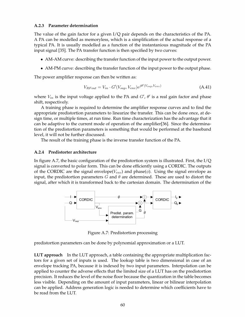
A.2.3 Parameter determination
The value of the gain factor for a given I/Q pair depends on the characteristics of the PA.A PA can be modelled as memoryless, which is a simplification of the actual response of atypical PA. It is usually modelled as a function of the instantanious magnitude of the PAinput signal [35]. The PA transfer function is then specified by two curves:
• AM-AM curve: describing the transfer function of the input power to the output power.
• AM-PM curve: describing the transfer function of the input power to the output phase.
The power amplifier response can then be written as:
VRFout = Vin ·G′(Vsup, Venv)ejθ′(Vsup,Venv) (A.41)
where Vin is the input voltage applied to the PA and G′, θ′ is a real gain factor and phaseshift, respectively.
A training phase is required to determine the amplifier response curves and to find theappropriate predistortion parameters to linearize the transfer. This can be done once, at de-sign time, or multiple times, at run time. Run time characterization has the advantage that itcan be adaptive to the current mode of operation of the amplifier[36]. Since the determina-tion of the predistortion parameters is something that would be performed at the basebandlevel, it will not be further discussed.
The result of the training phase is the inverse transfer function of the PA.
A.2.4 Predistorter architecture
In figure A.7, the basic configuration of the predistortion system is illustrated. First, the I/Qsignal is converted to polar form. This can be done efficiently using a CORDIC. The outputsof the CORDIC are the signal envelope(Venv) and phase(φ). Using the signal envelope asinput, the predistortion parameters G and θ are determined. These are used to distort thesignal, after which it is transformed back to the cartesian domain. The determination of the
CORDICI
Q
Predist. param. determination
Venv
θG
φCORDIC
IpQp
Vsup
Figure A.7: Predistortion processing
predistortion parameters can be done by polynomial approximation or a LUT.
LUT approach In the LUT approach, a table containing the appropriate multiplication fac-tors for a given set of inputs is used. The lookup table is two dimensional in case of anenvelope tracking PA, because it is indexed by two input parameters. Interpolation can beapplied to counter the adverse effects that the limited size of a LUT has on the predistortionprecision. It reduces the level of the noise floor because the quantization in the table becomesless visible. Depending on the amount of input parameters, linear or bilinear interpolationcan be applied. Address generation logic is needed to determine which coefficients have tobe read from the LUT.
60

Polynomial approach In the polynomial approach, the inverse PA transfer function is de-scribed as a polynomial in the PA characterization parameters. The order of this polynomialdepends on the amount of non-linearity that has to be suppressed. Typically, it ranges from3rd to 9th order. The predistortion gain can then be determined using:
gi(Vsup) =K∑j=0
ajVjsup (A.42)
G =L∑i=0
gi(Vsup)Vienv (A.43)
In these equations, aj represents a coefficient that is determined during the training phase,and K and L are the order of the Vsup and Venv polynomials.Both in the LUT and polynomial approach a CORDIC is required to enable coordinate systemtransformations. To vectorize the processing, a vector CORDIC operation would have to beavailable.
61

B EVPC code example of decimation using the DRF
evp_drf_init(M, PmodM, PdivM, nv, KmodM, KdivM);
evp_drf_write(*inp++);
evp_drf_write(*inp++);
evp_drf_write(*inp++);
evp_drf_write(*inp);
for(int i=0; i<nOut-1; i++){
evp_drf_barrier();
t1 = evp_vadd_16(evp_drf_read0(), evp_drf_read1());
acc = evp_vmac_i16(zero, t1, evp_vbcst_16(*coef++));
t1 = evp_vadd_16(evp_drf_read0(), evp_drf_read1());
acc = evp_vmac_i16(acc, t1, evp_vbcst_16(*coef++));
t1 = evp_vadd_16(evp_drf_read0(), evp_drf_read1());
acc = evp_vmac_i16(acc, t1, evp_vbcst_16(*coef++));
t1 = evp_vadd_16(evp_drf_read0(), evp_drf_read1());
acc = evp_vmac_i16(acc, t1, evp_vbcst_16(*coef++));
t1 = evp_vadd_16(evp_drf_read0(), evp_drf_read1());
acc = evp_vmac_i16(acc, t1, evp_vbcst_16(*coef++));
// Write next stage
evp_drf_write(*inp++);
evp_drf_write(*inp++);
evp_drf_write(*inp++);
evp_drf_write(*inp);
*OutPtr++ = acc;
coef = coef_orig;
}
evp_drf_barrier();
t1 = evp_vadd_16(evp_drf_read0(), evp_drf_read1());
acc = evp_vmac_i16(zero, t1, evp_vbcst_16(*coef++));
t1 = evp_vadd_16(evp_drf_read0(), evp_drf_read1());
acc = evp_vmac_i16(acc, t1, evp_vbcst_16(*coef++));
t1 = evp_vadd_16(evp_drf_read0(), evp_drf_read1());
acc = evp_vmac_i16(acc, t1, evp_vbcst_16(*coef++));
t1 = evp_vadd_16(evp_drf_read0(), evp_drf_read1());
acc = evp_vmac_i16(acc, t1, evp_vbcst_16(*coef++));
t1 = evp_vadd_16(evp_drf_read0(), evp_drf_read1());
acc = evp_vmac_i16(acc, t1, evp_vbcst_16(*coef++));
*OutPtr++ = acc;
Figure B.1: A code section performing decimation using the DRF. (K = 10, M = 3)
62

C Speedup compared to symmetric Bose
0 10 20 30 40 50 60 70 800
1
2
3
4
5
6
M =2
M =3
M =4
M =5
M =6
M =7
M =8
M =9
M =10
M =11
M =12
M =13
M =14
M =15
M =16
Filter length (K)
Sp
ee
du
p
2
3
4
5
6
7
8
9
10
11
12
13
14
15
16
Figure C.1: Speedup compared to symmetric Bose. P = 16, E = 4
0 5 10 15 20 25 30 35 400
1
2
3
4
5
6
M =2
M =3
M =4
M =5
M =6
M =7
M =8
Filter length (K)
Sp
ee
du
p
2
3
4
5
6
7
8
Figure C.2: Speedup compared to symmetric Bose. P = 8, E = 4
63

References
[1] J. W. Plunkett, Plunkett’s Telecommunications Industry Almanac 2010 Edition. PlunkettResearch, Ltd., 2008, 2009.
[2] Mobilen 50 Ar, “Facts about the mobile. a journey through time.” http://www.mobilen50ar.se/eng/press.asp, Oct. 2006.
[3] C. V. Mobile, “Cisco visual networking index: Global mobile data traffic forecast update,2009-2014.” https://www.cisco.com/en/US/solutions/collateral/ns341/ns525/ns537/ns705/ns827/white_paper_c11-520862.pdf, Feb. 2010.
[4] C. van Berkel, “Multi-core for mobile phones,” in Proc. Design, Automation and Test inEurope Conference and Exhibition (DATE), 2009.
[5] B. Bougard, B. De Sutter, S. Rabou, D. Novo, O. Allam, S. Dupont, and L. Van der Perre,“A coarse-grained array based baseband processor for 100mbps+ software defined ra-dio,” in Proceedings of the conference on Design, automation and test in Europe, pp. 716–721,ACM, 2008.
[6] Y. Lin, H. Lee, M. Woh, Y. Harel, S. Mahlke, T. Mudge, C. Chakrabarti, and K. Flautner,“SODA: A Low-power Architecture For Software Radio,” in International Symposium onComputer Architecture: Proceedings of the 33 rd annual international symposium on ComputerArchitecture, Association for Computing Machinery, Inc, One Astor Plaza, 1515 Broad-way, New York, NY, 10036-5701, USA,, 2006.
[7] C. Smith and D. Collins, 3G wireless networks. McGraw-Hill Professional, 2002.
[8] S. Sesia, I. Toufik, and M. Baker, LTE, The UMTS Long Term Evolution: From Theory toPractice. Wiley, 2009.
[9] E. Dahlman, S. Parkvall, J. Skold, and P. Beming, 3G evolution: HSPA and LTE for mobilebroadband. Academic Press, 2008.
[10] B. A. Horlin, F., Digital Compensation for Analog Front-Ends: A New Approach to WirelessTransceiver Design. Wiley, 2008.
[11] S. Park, “Principles of sigma-delta modulation for analog-to-digital converters,” Mo-torola Application Notes APR8, 1999.
[12] J. C. Candy, “An overview of basic concepts,” Delta-Sigma Data Converters, IEEE Press,New York, NY, 1997.
[13] G. Fettweis, M. Lohning, D. Petrovic, M. Windisch, P. Zillmann, and W. Rave, “DirtyRF: a new paradigm,” International Journal of Wireless Information Networks, vol. 14, no. 2,pp. 133–148, 2007.
[14] W. Tuttlebee, Software defined radio: enabling technologies. Wiley, 2002.
[15] T. Hentschel, M. Henker, and G. Fettweis, “The digital front-end of software radio ter-minals,” IEEE Personal Communications, vol. 6, no. 4, pp. 40–46, 1999.
[16] G. Hueber, G. Strasser, R. Stuhlberger, K. Chabrak, L. Maurer, and R. Hagelauer, “AMulti-Mode Capable Receive Digital-Front-End for Cellular Terminal RFICs,” in IEEEMTT-S International Microwave Symposium Digest, 2006, pp. 793–796, 2006.
64

[17] K. Van Berkel, F. Heinle, P. Meuwissen, K. Moerman, and M. Weiss, “Vector process-ing as an enabler for software-defined radio in handheld devices,” EURASIP Journal onApplied Signal Processing, vol. 16, p. 2613, 2005.
[18] J. Proakis and D. Manolakis, Digital signal processing: principles, algorithms, and applica-tions. Pearson Education, Inc., New Jersey, USA, 2007.
[19] R. Crochiere and L. Rabiner, “Optimum FIR digital filter implementations for decima-tion, interpolation, and narrow-band filtering,” IEEE Transactions on Acoustics, Speechand Signal Processing, vol. 23, no. 5, pp. 444–456, 1975.
[20] M. Coffey, “Optimizing multistage decimation and interpolation processing,” IEEE Sig-nal Processing Letters, vol. 10, no. 4, pp. 107–110, 2003.
[21] E. Hogenauer, I. ESL, and C. Sunnyvale, “An economical class of digital filters for dec-imation and interpolation,” IEEE Transactions on Acoustics, Speech and Signal Processing,vol. 29, no. 2, pp. 155–162, 1981.
[22] A. Kwentus, Z. Jiang, and A. Willson Jr, “Application of filter sharpening to cascadedintegrator-combdecimation filters,” IEEE Transactions on Signal Processing, vol. 45, no. 2,pp. 457–467, 1997.
[23] J. Eklundh, “A fast computer method for matrix transposing,” IEEE Transactions on Com-puters, vol. 100, no. 21, pp. 801–803, 1972.
[24] G. Goldbogen, “Prim: A fast matrix transpose method,” IEEE Transactions on SoftwareEngineering, pp. 255–257, 1981.
[25] Y. Jung, S. Berg, D. Kim, and Y. Kim, “A register file with transposed access mode,” inComputer Design, 2000. Proceedings. 2000 International Conference on, pp. 559–560, 2000.
[26] A. Shahbahrami, B. Juurlink, and S. Vassiliadis, “Matrix register file and extended sub-words: two techniques for embedded media processors,” in Proceedings of the 2nd con-ference on Computing frontiers, p. 179, ACM, 2005.
[27] B. Hanounik and X. Hu, “Linear-time Matrix Transpose Algorithms Using Vector Reg-ister File With Diagonal Registers,” in Proceedings of the 15th International Parallel & Dis-tributed Processing Symposium, p. 36, Citeseer, 2001.
[28] N. Jayasena, M. Erez, J. Ahn, and W. Dally, “Stream register files with indexed access,”in High Performance Computer Architecture, 2004. HPCA-10. Proceedings. 10th InternationalSymposium on, pp. 60–72, 2004.
[29] Van Der Horst, M. and Van Berkel, K. and Lukkien, J. and Mak, R., “Recursive Filter-ing on a Vector DSP with Linear Speedup,” in Proceedings of the 2005 IEEE InternationalConference on Application-Specific Systems, Architecture Processors, p. 386, IEEE ComputerSociety, 2005.
[30] V. Valimaki and T. Laakso, “Principles of fractional delay filters,” in Proceedings of theIEEE International Conference on Acoustics, Speech and Signal Processing (ICASSP’00), 2000.
[31] L. Milic, Multirate Filtering for Digital Signal Processing: MATLAB Applications. Informa-tion Science Publishing, 2009.
[32] N. Ceylan, Linearization of power amplifiers by means of digital predistortion. PhD thesis,University of Erlangen-Nrnberg, 2005.
65

[33] F. Wang, A. Yang, D. Kimball, L. Larson, and P. Asbeck, “Design of wide-bandwidthenvelope-tracking power amplifiers for OFDM applications,” IEEE Transactions on Mi-crowave theory and techniques, vol. 53, no. 4, pp. 1244–1255, 2005.
[34] F. Raab, P. Asbeck, S. Cripps, P. Kenington, Z. Popovic, N. Pothecary, J. Sevic, andN. Sokal, “Power amplifiers and transmitters for RF and microwave,” IEEE Transactionson Microwave Theory and Techniques, vol. 50, no. 3, pp. 814–826, 2002.
[35] S. Cripps and S. Cripps, RF power amplifiers for wireless communications. Artech HouseNorwood, MA, 1999.
[36] K. Muhonen, M. Kavehrad, and R. Krishnamoorthy, “Look-up table techniques foradaptive digital predistortion: adevelopment and comparison,” IEEE transactions onvehicular technology, vol. 49, no. 5, pp. 1995–2002, 2000.
66