eindhoven university of technology master design … · ... analog to digital and digital to analog...
TRANSCRIPT

Eindhoven University of Technology
MASTER
Design and simulation of an 18-bit CMOS DA Converter
Veenstra, H.
Award date:1991
DisclaimerThis document contains a student thesis (bachelor's or master's), as authored by a student at Eindhoven University of Technology. Studenttheses are made available in the TU/e repository upon obtaining the required degree. The grade received is not published on the documentas presented in the repository. The required complexity or quality of research of student theses may vary by program, and the requiredminimum study period may vary in duration.
General rightsCopyright and moral rights for the publications made accessible in the public portal are retained by the authors and/or other copyright ownersand it is a condition of accessing publications that users recognise and abide by the legal requirements associated with these rights.
• Users may download and print one copy of any publication from the public portal for the purpose of private study or research. • You may not further distribute the material or use it for any profit-making activity or commercial gain
Take down policyIf you believe that this document breaches copyright please contact us providing details, and we will remove access to the work immediatelyand investigate your claim.
Download date: 06. Aug. 2018

CoachPeriod of work
Eindhoven University of TechnologyDepartment of Electrical Engineering
Digital systems EB
GRADUATION REPORT
Hugo Veenstra
Design and simulation of an IS-bitCMOS DA Converter
Prof. dr. ir. Rudy J. van de PlasscheApril 15 - December 12, 1991
© N. V. Philips' Gloeilampenfabrieken 1991All rights are reserved. Reproduction in whole or in part is
prohibited without the wl'itten consent of the copyright owner.

Abstract
The introduction of digital home audio systems, such as the Compact Disc, has greatlystimulated the development of high accuracy Analog to Digital and Digital to AnalogConverters. Many techniques have been invented during the last few years to improvethe DA conversion accuracy. As an example, the dynamic element matching technique[7J, invented by van de Plassche, is still used in Philips 14 and 16 bit DAC's. The mainidea behind this technique is to use time averaging to cancel errors that arise in currentdivision. However, there are some drawbacks to this technique:
• A high supply voltage is needed, due to the cascading of current dividers;
• The time averaging technique requires external capacitors.
To overcome the supply voltage problem, van de Plassche presented already in 1986 asystem setup for a low voltage, high accuracy DAC in a patent [1J. This patent describes some general ideas for a DAC, achieving high accuracy by current calibration.It is only developed up to a block diagram, no implementation is given. The subjectof this thesis is to develop the analog part of a DAC using the ideas from [1J with highaccuracy, low voltage operation and without external components.
The main analog part to achieve high accuracy is a precision current mirror, whichmust divide an input current by 2 with a relative error below 10-6 • For this circuit,existing current mirrors do not fulfill this demand. Combining the dynamic elementmatching technique with the geometric averaging technique gives the solution for aprecision current mirror with the desired accuracy. Using a high switching frequencyfor the dynamic element matching, the time averaging capacitor can be integrated onchip.
Other analog parts are analyzed, such as a low noise current to voltage converter,implemented as a folded cascode opamp, a sensitive error current detector, an inherently monotonic resistive voltage divider and a reference voltage source.
As a result, all the important analog parts of an 18 bit CMOS DAC are described atMOS transistor level, including some important simulation results. However, no starthas yet been made with the layout of this DAC.

Preface
During the past months, it was a great pleasure to work at the PHILIPS ResearchLaboratories. I would like to thank Prof. dr. ir. Rudy van de Plassche for giving methe opportunity to do my graduation work under his supervision. Furthermore, I amgreatly thankfull to my roommate, Toon Bogers, for his moral and technical support.Of course, there are many other members of the laboratory who helped me with ideasand advise. Without all these guidance, I would probably have been lost within theextensive world of PHILIPS.
Eindhoven, November 13, 1991Nederlandse Philips Bedijven B.V.

Contents
1 Introduction
2 Basic DAC system setup2.1 Demands made for the DAC .2.2 Choosing a technology . .2.3 Global system overview2.4 The calibration procedure2.5 Errors of the bit currents
3 Structure of the bit currents3.1 MOS generalities ....3.2 Different architectures . . .3.3 The cascoding technique . .3.4 Temperature dependence of the bit currents3.5 Implementation of the bit currents . . . . .
4 Adjusting the bit currents4.1 Derivation of the required calibration range4.2 Modifications to the current sources4.3 The resistive divider . . . . . . . . .
5 Operational amplifiers5.1 The differential pair .5.2 Demands for the output Opamp5.3 Enhancing the gain . . . . . . . .5.4 The folded cascode configuration5.5 Frequency compensation . . .5.6 Detection of the error current
6 The reference source6.1 DC analyses of the source . . . . . . . . . . . . .6.2 Temperature dependence of the reference source6.3 The design procedure .
G.4 Influence of technology variations . .G.5 Creation of different output voltages
7
8
889
1013
161617192225
29293233
37374142
444648
525256596065

6
7 The precision current mirror7.1 Accuracy of the standard current mirror7.2 Dynamic element matching . . . . . . .7.3 Enhancing the current mirror accuracy.7.4 Implementation of the current mirror .
8 Glitches due to switching8.1 Switching in the precision current mirrors8.2 Switching the bit currents . . . . . . . . .
9 Conclusions
A Current source transistor parameters
B Folded cascode schematic diagram
C Current mirror schematic diagram
CONTENTS
6868707273
767676
80
85
87
89

Chapter 1
Introduction
This report reflects the work, executed at the PHILIPS Research Laboratories duringthe period of April 1991 - December 1991. At the group Brandsma of this laboratory,research and engineering is carried out for the design of future radio and data transmission systems. These systems are mostly based on digital data transfers, and thereforeAD- and DA Converters are of great importance.
Up till now, the range of the PHILIPS DA Converters is limited to 16 bits. As ascientific project, the goal is to extend this range up to 18 bits, at a converter speed of200 kHz. In [1], van de Plassche presents some new ideas for the calibration of a DAC,in order to enhance its accuracy. This patent forms the basis for this project. Startingfrom here, a complete 18 bit DAC is designed in a standard CMOS process.
To reach the demands for 18 bits accuracy, a structured analysis of the basic partsof the converter is presented, existing of successively:
• The general system setup;
• Implementation and calibration of the bit currents;
• The different operational amplifiers used;
• Switching of the bit currents;
• A newly designed voltage reference source.
The converter design is based on the Philips C200 process, but can be implemented inany Clvl0S process. Only schematic diagrams and simulation results are presented, nolayout has yet been designed for the DAC.
..,

Chapter 2
Basic DAC system setup
The DAC is based on the ideas presented by van de Plassche in [1]. Paragraph 2.1describes the demands for the DAC.
Already in an early stage, the used technology has to be chosen, because this greatlyinfluences the architecture of the DAC. Paragraph 2.2 declares the chosen technology.A global system overview is given in paragraph 2.3. The calibration procedure isexplained in paragraph 2.4. At last, the errors of the bit currents after calibration arediscussed.
2.1 Demands made for the DAC
There are several demands which the DAC has to fulfill, given in order of importance:
• High resolution: up to 18 bit;
• Medium speed: up to 200 kHz., in this way 4-fold oversampling in digital audioapplications is possible;
• Low supply voltage operation: Vdd ~ 5 V;
• No external components;
• Low power consumption;
• Small die size.
2.2 Choosing a technology
To reach the demands of low-power, low-voltage operation, the choice of a CMOSprocess is obvious. The main drawback of the CMOS technology in DAC applicationsis the offset voltage, inherently present between two similar transistors. Precautionshave to be taken, by using setups non-sensitive for this offset voltage.The design is based on the Philips C200 process, which has as main device parameters:
• Wmin = 1.25 pm;
• L min = 1 pm;

2.3. GLOBAL SYSTEM OVERVIEW
VoVO
9
18-9
P&IIIIive dividerbit 18-9
Calibratedbit currents
bit 8-2 bit 1
Referencevoltages
Calibratedtail current
Precision currentmirrors
Figure 2.1: Total DAC block diagram
• I-lnCox = 73. 10-6 AIV2;
• I-lpCox = 27. 10-6 AIV2;
• n-well technology;
• VT,NMOS = 0.8 V;
• VT,PMOS = 1.1 V;
• threshold voltage modulation due to the body effect 0.3 V IV.
The n-well technology makes that the bulk of the PMOS transistors can be connectedanywhere, while the bulk of the NMOS transistors will always be connected to ground.
2.3 Global system overview
The DAC can be divided into parts, each with a specific function. This gives the setupfrom figure 2.1.The DAC contains some standard parts, which are present in practically all converters:
• Bit current sources, with binary scaled output currents, for bit 1-18. Here, bit 1is the Most Significant Bit (MSB).
• Bitswitches, which connect the output current of the bit current sources to theI IV converters. These switches are directly controlled by the digital input code.
• I IV Converters, which convert the converter output current into the output voltages Vo and Vo .

10 CHAPTER 2. BASIC DAC SYSTEM SETUP
• To obtain precise currents, the current sources are biased with reference voltages.
To reach 18 bit accuracy, the output currents of the bit 2-8 current .sources are calibrated. Also, the tail current of bit 9-18, the so called tail current, is calibrated.To calibrate the bit current sources, precision current mirrors are used. The MSBcurrent acts as a reference current, it is used as input current for a precision currentmirror. This mirror divides the input current by two with very high precision, the relative output current error is below 10-6 • This way, a high precision reference currentis generated for the bit-2 current source. The actual value of the bit-2 current sourceis compared with this reference current, and if necessary the bit-2 current is adjusted.Once the bit-2 current is calibrated, this current can act as input current for the highprecision current mirror, in order to calibrate the bit-3 current. The same procedureas for the bit-2 current is now repeated.
The sum of the passive divider bit currents is:
18
2:: in = i 8 - i 18n=9
The tail current is calibrated to the bit-8 current. To make the calibration correct, anextra bit-18 current is needed. The tail current is then equal to the bit-8 current.The 18 bit currents are obtained in the following way:
• Bit 1, the MSB, is obtained using reference voltages, and therefore has a highstability. This current is designed to have minimal sensitivity for voltage andtemperature variations, and is used as a reference current.
• Bit 2-8 are adjusted to. 1.Zn = '2 .Zn-1, n = 2..8
using precision 1:2 current mirrors and the calibration circuitry.
• Bit 9-18 are obtained using a passive divider. The sum of these bit currents plusa dummy bit-18 current, also called 'tail current', is adjusted to the bit-8 currentusing a precision 1:1 current mirror.
The use of two I/V converters, leading to a differential output, has several advantages:
• doubled output voltage swing;
• reduction in noise contribution of the output opamp by 3 dB.
The MSB-current is set to be 500 J.LA, which results in a LSB-current of 2-17 .500 J.LA =3.81 nA. All bits 2-8 and the tail current are calibrated with a 1 nA resolution so,with approximately 1/4 LSB accuracy.
2.4 The calibration procedurer\.l-y
To achieve a fast calibration cycle, five current mirrors are used in stead of one. Eachof these mirrors is designed optimally for its input current and desired accuracy.

2.4. THE CALIBRATION PROCEDURE
InIn-Im
Im
11
calibrationready
clock
1 2Precision current mirror
Figure 2.2: The calibration procedure
Using five current mirrors A-E, calibration of the total DAC can take place in twostates. Table 2.1 explains the actions taken in each state.
There are two types of current mirrors used:
• mirrors A-D are 1:2 mirrors; they divide the input current by 2;
• mirror E is a 1:1 mirror.
One calibration cycle exists of two states, 0 and 1. During state 0 and state 1, the bit 2to bit 8 and tail currents are calibrated using the algorithm explained below, illustratedin figure 2.2.
The bit current In can be adjusted using coarse and/or fine current steps. The coarsestep value is smaller then the sum of all the fine steps.
Distinction has to be made between the first calibration cycle and the next calibration cycles. During state 0 of the first calibration cycle, the following steps are takenfor each current mirror:
• set i fine to ifine,max;
• set icoarlle to icoarlle,min;
• while In < 1m do step-increase icoarlle;
• while not ready do step-decrease ifine;
• if all mirrors are ready, change state 0 -+ 1.
So, after state 0 of this first calibration cycle, the error of 12 is divided uniformly withinone step value of ifine or ±1/4 LSB: 12 is calibrated. Whether the calibration is ready

12
Fint cal cycle
CHAPTER 2. BASIC DAC SYSTEM SETUP
ABC D E
N
N
Step-inc~ tine
N
Btep-dec~ tine
Figure 2.3: Flowchart of the calibration cycle
or not is detected by an error detection circuit, which has to detect error currents of1/4 LSB or 1 nA.From now on, steps are taken as shown in the flowchart of figure 2.3.
As can be seen in the flowchart, the state only swaps between 0 and 1 when allbits are calibrated. If no calibration is necessary, the 'calibration ready'-signal willimmediately be active. In this way, the ripple on the bit currents, due to the discreteadjustment of the bit currents, is limited to a minimum.
The five current mirrors all perform this calibration algorithm simultaneous. Whenall calibrations are ready, alternation can take place between state 0 and state 1. Thus,the bits which serve as reference currents in state 0 are calibrated in state 1 and viceversa.
After power on, it takes some time before all the bits are calibrated to the rightreference. For example, to calibrate bit 8, bit 7 must already be calibrated, becausethis bit is used as reference. As can be seen in table 2.2, after 4 calibration cycles theDAC is completely calibrated.

2.5. ERRORS OF THE BIT CURRENTS
The conditions necessary to let this algorithm find a solution are:
• the situation 1m = In falls within the range of In;
13
• the range of the fine current is greater then the step value of the coarse current.
In the next chapters, the analog circuits making the execution of this algorithmpossible are described.
2.5 Errors of the bit currents
After calibration, the error of the bit 2 current is divided uniformly within plus andminus one step-value of the fine adjust current, so the accuracy is ±1/4 LSB. Becausethe bit 2 current is used as reference for calibration of the bit 3 current, errors add.For each next bit calibrated, an extra error is introduced. This continues 8 times, upto the tail current. A precise evaluation of the error in each bit follows next.
Given the MSB current IMsB = I. After calibration, for the bit 2 current holds:
Ih = 2 + h(x) (2.1 )
Here, h(x) represents the error, divided uniformly within ±1/4 LSB. Because alreadycalibrated bits are used as reference for next bits, the following relations exist:
!JI h(x)
(2.2)= 22 + -2- + !J(x)
14I h(x) !J(x) f ( ) (2.3)= 23 +~+-2-+ 4 x
(2.4)
IsI t fk(X) (2.5)- 27 + 2S- k
k=2
(2.6)
All the error functions fk(X), k = 2···8, are divided uniformly within ±1/4 LSB. Inworst case, the error in bit 8 now simply becomes:
(2.7)
So, in worst case, bits 2 - 8 all have an error smaller then 1/2 LSB.

14 CHAPTER 2. BASIC DAC SYSTEM SETUP
The tail current is calibrated to the bit 8 current using a 1 : 1 current mirror.Therefore, the error of the tail current is the sum of the bit 8 error and a new uniformlydivided error ftai/(X), also uniformly divided within ±1/4 LSB: .
(2.8)
So, the error in the tail current is in worst case 3/4 LSB. Bit 9 is made of half the tailcurrent, so the error can again be kept within 1/2 LSB. In this way, the converter ismonotonic.
In practice, there are also errors in the division factor '2'. This error is relativelyseen the most important at the first division. The error in bit 2, due to the calibrationalgorithm is 1/4 LSB. To assure monotonicity, the total error in bit 2 must remain lessthen 1/2 LSB, so the maximum allowed error due to the division is 1/4 LSB. The bitcurrent from bit 2 is 217 LSB, so the division factor of the 1 : 2 current mirror A mustbe accurate within 1/219 == 2 . 10-6 .
The error in the division factor of current mirror B may be 22 times as big to cause thesame absolute error on the bit 4 current, mirror C may have a 24 times as big error,mirror D 26 times and mirror E 27 times.

2.5. ERRORS OF THE BIT CURRENTS
~ state 0 state 1
15
llllrror lin iotJt iin iotJt
A bit 1 bit 2 bit 2 bit 3B bit 3 bit 4 bit 4 bit 5C bit 5 bit 6 bit 6 bit 7D bit 7 bit 8 - -E - - bit 8 tail
Table 2.1: Use of the current mirrors
I after cal. cycle I1 state 01 state 12 state 02 state 13 state 03 state 14 state 0~ 4 state 1
bits calibrated I2
2,32,3,4
2,3,4,52,3,4,5,6
2,3,4,5,6,72,3,4,5,6,7,8
2,3,4,5,6,7,8,tail
Table 2.2: Calibrated bits after power on

Chapter 3
Structure of the bit currents
The main formulas, important in MOS technology design, are summarized in paragraph3.1. Next, different architectures for current sources are discussed. The cascodingtechnique, to enhance the output impedance of the current source, is explained inparagraph 3.3. The temperature dependence of the current source is discussed. Atlast, the structure of the current sources for bit 1-18 is given.
3.1 MOS generalities
For the MOS transistor, there are three main regions of operation. The current-voltagebehaviour for all these regions are summarized in formula 3.1, supposing an-channelMOST.
(3.1)
The + indicates that the term within the brackets only contributes to the formula whenit's value is positive.The different regions for the MOST are:
• Saturation region: (Vgs - VT ) > 0;
• Cutoff region
• Linear region
(Vgs - VT ) < 0;
(Vgs - VT ) > 0;
(vgd - VT) < 0;
(vgd - VT ) > 0;
(Vgd - VT) < 0 ;.
Thus, in the cutoff region, the current is always O. This situation is used as offconditionwhen the MOST is used as a switch.A correction to formula 3.1 must be made in the saturation region, to indicate thechannel length modulation:
Id = ~(vgs - VT)2(1 + 'xVds) (3.2)
1"'\4-The factor ,X IS approximately 0.01 for a NMOST with L = 5 f.lm, 0.02 for a PMOSTwith L = 5 f.lm and approximately the relation ,X "'" i is valid.

3.2. DIFFERENT ARCHITECTURES
d
17
g --e
B
Figure 3.1: MOS small signal equivalent
For small negative values of VgT , approximately -0.5 < VgT < 0.1 V the MOSTcomes in the subthreshold region. In this region, which is not included in formula 3.1,the drain current becomes
qVgTId "-' exp(--)
kT(3.3)
(3.4)
The threshold voltage VT is a function of the bulk voltage Vb. If the bulk voltageincreases with ~Vb, the VT changes approximately 0.3 . ~Vb.
The small signal equivalent of the MOST is given in figure 3.1. Here, parasiticcapacities are not yet included.
The transconductance 9m in the saturation region can be derived from equation3.2:
8~ MOT9m = 8~s = ;3(Vgs - VT) = V 2;3Id
Here, the channel length modulation is neglected. The gain conductance 9d comes fromthe same equation:
8Id )..Id9d = -- =
8Vds 1+ )..Vds
When 11:, is constant, the transconductance in the subthreshold region becomes:
Literature [2] gives a complete overview of general MOS theory.
3.2 Different architectures
(3.5)
(3.6)
In figure 3.2, three different architectures for constant current sources are shown, whichwill be discussed successively.
In all three cases, the transistors are assumed to be in the saturation region andthe drain voltage Vdn is assumed to be constant. For each situation, the sensitivity ofId for variations in Vg will be derived.

18
Case A:
CHAPTER 3. STRUCTURE OF THE BIT CURRENTS
Vdn Vdn Vdn
Vg --1 Vg --1 Vg --1 Tl
Van
R R
Vgp --1 T2
- -
A B C
Figure 3.2: Three basic current sources
Case B:
Id 5~t ~(Vg - VT - IdR )2
vffcJ = f%(Vg - VT - IdR)
[2i;Vg = V~ + VT + IdR
8Vg 18Id = v'2lJId + R
8Id v!21Jld gm8ll;, = 1+ R.j2f3Id = 1+ gmR
(3.7)
(3.8)
(3.9)
(3.10)
(3.11)
(3.12)
(3.13)
Comparing formulas 3.8 and 3.13, it is clear that for each R > 0, the sensitivity in caseB is smaller then in case A. Also, the sensitivity decreases for increasing R.In the DAC, it is necessary to implement a calibration algorithm. This implies that the

3.3. THE CASCODING TECHNIQUE 19
current must be available as input for a monitoring circuit. Besides, the goal is to beable to use the DAC without interruption for a calibration procedure. A setup whichmakes these demands realisable is to add an extra PMOST, as shown"in case C. Here,the voltage ~p is assumed to be constant.
Case C:
sat f3n(V; v: TT)2Id = 2" 9 - sn - YTn
sat f3p(V; v: TT)2Id = 2 - gp + sp - YTp
~n = Vsp + IdR
From these three equations, again the sensitivity can be derived.result:
fJId J2f3nf3pId
6~ = ~+ VlJ; + RJ2/3n{3pId
(3.14)
(3.15)
(3.16)
This gives the next
(3.17)
(3.18)
For the situation f3p -+ 00, the situation of case B returns; for smaller f3p the sensitivityis smaller compared to case B.
3.3 The cascading technique
To reach 18 bit accuracy for the total DAC, the accuracy of the MSB current must bein the order of 10-6 . To give sufficient freedom in the design of the calibration circuit,the current source will be designed to have an allowable variation in Vd of 1 V. Thisgives a desired output impedance rd = 1/9d ~ 106 O.
The output current of the current source is influenced by the drain voltage Vd, byway of the channel length modulation (see formula 3.2). The output conductance of aMOST can be derived using this formula:
(fJId ) 0 A 0 0
gd = 6Vds = 1 + Alids Id ~ AId
With A = 0.02 and the MSB current I~ = 500 #-lA, the output impedance of a PMOSTwith length L = 5 #-lm becomes 20 kO.A long MOST would be necessary to obtain the desired output impedance. This is notallowed, and a method to overcome this problem is to enhance the output impedanceby using a cascoded PMOST, as shown in figure 3.3.
The output impedance of the current source of figure 3.3 can be derived using thesmall signal schematic of figure 3.4.
Attention must be paid to the fact that the NMOS transistor T1 is situated underin the small signal schematic. Again it is assumed that the drain of T1 is connected toa constant voltage Vdn. Therefore this drain is connectC'd to ground in the small signalequivalent schematic diagram. Only variations in the drain voltage of the PMOST are

20 CHAPTER 3. STRUCTURE OF THE BIT CURRENTS
Vdn
Vg -1 Tl
Vsn
R
Vsp
Vgpl -1 T2
Vgp2 -1 T3
Figure 3.3: Cascaded current source
I
Output impedance
BJDlVpi!with cascode
Bell Z.. -I91 Output impedance
-B.,Vp2!
without cascadeS~ Z01
-
91 RI91 ~
latVpl t Output impedance
I dlat source
Zot
-
Figure 3.4: Small signal equivalent for the cascaded current source

3.3. THE CASCODING TECHNIQUE
I
21
Output impedancev
Figure 3.5: Generalized small signal equivalent
considered.
To calculate the output impedance, an imaginary voltage source is connected to theoutput. Now V / I gives the desired output impedances Zo2 and Zo3' This value can becalculated, using the following strategy:
• calculate the output impedance Zol at the source of T1;
• add R;
• calculate Zo2, the output impedance of the non-cascoded current source;
• now also the output impedance Zo3 of the cascoded current source can be calculated.
The controlled current source 9mVgs of T1 can directly be transformed into animpedance 1/9m because the control voltage vgs is the voltage across the source itself.This gives as result:
1Zol = (3.19)
9m +9d
From fornmla 3.19 comes the general conclusion that the input impedance at the sourceof a MOST is low.
To calculate Zo2, the simplified diagram of figure 3.5 is used.From figure 3.5 follows:
IVs =
9s
I = (V - V,)9d - 9m I9s
Combining these formulas gives:
Zo = V = 9d + 9m + 9sI 9d9s
Note that this result is generaly valid:
(3.20)
(3.21)
(3.22)

22 CHAPTER 3. STRUCTURE OF THE BIT CURRENTS
• to calculate the output impedance of the current source of figure 3.2.b, substitute1/9s = R;
• to calculate the output impedance Zo2 of the current source of figure 3.4, withoutcascode, substitute 1/9s = R + Zol;
• to calculate the output impedance Zo3 of the current source of figure 3.4, withcascode, substitute 1/9s = Zo2;
• to calculate the output impedance Zo4 at the drain of the NMOST of the currentsource of figure 3.4, with cascode, substitute:
1 1 1-=R+ +--9s 9m + 9d 9m + 9d~~
PMOST2 CascodeT3
A drawback of the cascoding technique is the extra VgT' required to let the cascodedMOST work in saturation. This results in a higher minimal supply voltage to let thecurrent source work properly.
3.4 Temperature dependence of the bit currents
III the current formula 3.1, the temperature dependence has two sources:
• the threshold voltage VT;
• the electron mobility J.Ln.
For the threshold voltage holds:
(3.23)
with
with
with
and
so that
ni = JNcNvcxp ( ;:; )
(3.24)
(3.25)
(3.26)
(3.27)
(3.28)

3.4. TEMPERATURE DEPENDENCE OF THE BIT CURRENTS 23
Also, from [3), for the bandgap Eg in silicon holds
E= 17 _ 4.73 .1O-4T 2
9 1. T + 636(3.29)
Combining these formulas gives:
(3.30)
From equation 3.29 it is clear that with increasing temperature Eg decreases. Fromequation 3.30, the first part increases linearly with the temperature while the secondpart decreases via the minus-sign with canst· T 'In(T3/2), so fa.,c;ter then the first partIncreases.
(3.31)
The Hatband voltage VFB has as temperature dependent part <PMS. In [6] is explained that the temperature dependence of this part depends on the type of dope ofthe gate:
• If the. gate has the same type of dope as that of the substrate, the relation
8<PMS <PMS8'i'=T
is valid;
• If the gate has an opposite dope as that of the substrate, the temperature dependence is the same as that of a pn-diode. This will be analyzed in chapter 6, hereonly the result is given:
..I.. !b.8<PMS 3k 'f'MS - q-8-T- = - q + ----::T=--l.- (3.32)
For a silicon pn-diode at T = 293 K, the temperature coefficient becomes-1.8 mVjK.
As a result, the threshold voltage has a negative temperature coefficient. This meansthat the 'beginning point' of the Id - Vgs-curve decreases with raising temperature.
From [3], the temperature dependence of J.l consists of two parts:
• lattice scattering J.l1 I"V T-3/2;
• impurity scattering J.li I"V T3/2.
(3.33)
The following relation holds:1 1 1-=-+J.l J.lI J.l i
In a semiconductor with few impurities, the mobility shall be limited by the latticescattering, so J.l1 shall dominate and J.l I"V T-3/2. Thus, J.l has a negative temperaturecoefficient. Therefore, the slope of the I d - ~s-curve decreases with raising temperature.

24 CHAPTER 3. STRUCTURE OF THE BIT CURRENTS
Aug 29, 199115:32:37
NMOS diode temperature dependenoe
(LIN) soom aotive
40.0u 4----+----f---------1L---+----l-----+-----f--Hr----I
30.0u -+----+----+-----J---+-----+----+---cI#---+----1
20 .Ou -+----+----+-----J---+------+---r--+----+~'7"____1
10.0u -+-----+-----+-----J---+---"""79."'-+-----::7"'-'+----+--___1
- Subvar ,,: 10.0TEMP: 20.0
2,,: 10.0TEMP: 50.0
3,,: 10.0
TEMP: 80.04
,,: 20.0
TEMP: 20.05
", 20.0TEMP: 50.0
6,,: 20.0TEMP: 80.0
- yl-axia - 50.0u -,-----,-------,------,---,.-----,-----,-------,----,-"
I(NK l\D)
0.0 -L----I---4---iiiiiiiiii!~~===L-___l_-~--__t_--J600.Om 800.Om 1.0 1.2 1.4
700.0m 900.Om 1.1 1.3
(LIN) VG
Figure 3.6: Temperature dependence of a MOST
Combining the two temperature effects results in Id - Vgs-curves with a point of interception. A simulated example of the temperature dependence of a NMOS transistoris given in figure 3.6.
As can be seen, the MOST can have a positive or a negative temperature coefficient,dependent on the bias voltages. In between these two regions, there is a point wherethe MOST operates temperature-independent. This phenomenon is used for realizingthe bit currents, resulting in current sources almost independent of the temperature.
Besides, the temperature independent point appears at the same Vgs for different W / L ratio's. This can be explained using the MOST current equation 3.1 in thesaturation region. Temperature dependence exists only in I-ln and VT, so at differenttemperatures T1 and T2 holds:
W 2T1 : II = I-ln,Tl Coz 2L (Vgs - VT,TJ (3.34)
W 2T2 : 12 = I-ln,T2Coz 2L (Vgs - VT,T2) (3.35)
The temperature independent point is allocated at the interception point, so at h = 12 ,
this gives:(3.36)
Formula 3.36 is independent of Wand L. From this formula the voltage Vgs at whichthe MOST is biased temperature independent can be solved. The result is formula3.38, independent of the transistor sizes, and also independent of the absolute value of

3.5. IMPLEMENTATION OF THE BIT CURRENTS
the electron mobility /-In.v JPn,Tl V
T,T2 - IJn,T2 T,T1
~8 = ------'---;::;=::====--1 - JlJn,TJ
IJn,T2
Substituting /-In '" T-3/2 gives as final solution:
(T ) -3/4
VT,T2 - ~ VT,TI~8 = ---....o(-T"-'--)---=3-;-/4:---
1- ~
25
(3.37)
(3.38)
As an example, the temperature independent point from figure 3.6 can be verified.The MOSCA program is used to calculate the threshold voltages at T1 = 293 K andT2 =353 K, with as result VT,TJ =0.828 V and VT ,T2 = 0.766 V. With formula 3.38,the temperature independent point becomes 1.24 V.
3.5 Implementation of the bit currents
As shown in the block diagram of figure 2.1, the bit currents can be divided into threeparts:
• The MSB current, acting as reference current.
• Bit currents 2-8, which are adjustable.
• Bit currents 9-18, formed in a passive divider.
The passive divider consists of an array of equal transistors, all with equal ~s as shownin figure 3.7. Only bit 18,17, 9 and the dump current are shown. Note that nm3 has a512 times larger size then nm4. The structure of a current source with cascode can berecognized. The LSB current, bit 18, is formed by a single transistor current. To formthe bit currents of bit 17 to 9, for each next bit the number of transistors connected inparallel is doubled. Together with a LSB dump current, in total B = 1024 transistorsare needed.The passive divider is implemented as 10 bits. The choice of 10 bits is based uponliterature [4], where a detailed analysis of the passive divider accuracy is presented.
The main result of [4] is formula 3.39 giving the variance of h, the sum of b draincurrents. The average current flowing in each transistor is I mean •
u(h) = -.LU(VT)V (B - b)bImean kT B
(3.39)
According to [5], the variance U(VT) in VT of a single transistor can be approximated by:
(TT ) _ 16mV
u VT - VWL (3.40)
For the MSB, an accuracy within ±0.5 LSB is desired. To have a yield of at least68% a variance of U(IB) = 0.5hsB is allowed, assuming a normal distribution. With

26 CHAPTER 3. STRUCTURE OF THE BIT CURRENTS
bit 18 bit 17 bit 9
dump
1I'C-w, LO-l, MOLT-I
lro_, LO-l, MOLT-2
Vbias,n
- If-----r--<:JVbulkVbias,plC>--------j
VbiaS'P2~
From current mirror E
Figure 3.7: Implementation of the passive divider
B = 1024, b = 512, q/kT = 40 V-I and Imean = hSB follows from 3.39 thata(VT ) ~ 0.8 mV. This can be achieved with WL ~ 400. Square transistors withW = L = 20 J.lm satisfy this demand. This result also explains the 10 bit limitationof the passive divider; with higher accuracy the allowed variance of the bit currentsdecreases.
The bit currents for the remaining bits n = 1 to 8 are formed using 256/2n-
1 cascoded current sources in parallel. Thus in total 511 equal cascoded current sourcesare used, all with equal bias voltages. The MSB current source is shown in figure 3.8.Temperature independent biasing is applied for the transistors. The single transistorcurrent is 500/256 J.lA. Reference voltages va, vb and vc are chosen so that all transistors operate in the saturation region and within 5 volt supply voltage, as shownin figure 3.8. This leaves a voltage across the current source resistor of 0.3 V, soRn = 2n
-1 ·600 n, so RI = 600 n. With the aid of a simulation program, the
temperature independent bias point is fixed at the desired current and voltage.
The output impedance from the current source can be calculated using formula3.22. The parameter values for this formula are calculated with the MOSCA program,and are summarized in table 3.1.
For the MSB, 256 equal transistors are placed in parallel, so the conductances gm
and gd must be multiplied by this value to calculate the MSB current source outputimpedance.With R = 600 n, the results for the MSB current source are:Impedance at source(NMOS):
1Zol = = 201 n
gm +9d

3.5. IMPLEMENTATION OF THE BIT CURRENTS 27
+ec 3vnTvb)WU-7.25,LU-12,MULT-256
WU-13.5,LU-4,MULT-256
+ec 2vnTvc)
Figure 3.8: Implementation of the MSB current
9m 9d VT VqtNMOS 19 ·10 -(j 8.10 -9 1.49 0.20PMOS 7.10-6 15.10-9 1.17 0.54
Cascode 18.10-6 54.10-9 1.33 0.22
Table 3.1: Main parameters of the current source transistors

28 CHAPTER 3. STRUCTURE OF THE BIT CURRENTS
Output impedance without cascode:
Zo2 = gd + gm + gs = 625 kngdgs
With cascode, the output impedance becomes
Zo3 = gd + gm + gs = 206 Mngdgs
The output impedance at the drain of the NMOST is
Zo4 = gd + gm + gsgdgs
With
1 1 1- = R + + = 1.15 kngs gm + gd gm + gd
"-v----' "-v----'PMOST2 CascodeTJ
follows Zo4 = 3.1 Mn. For bit n, n = 1···8, the impedances must be multiplied by n.
'With a cascode, the results satisfy the demand Zo ~ 1 Mn at both drains. Alltransistors are designed to be in saturation. The output voltage of the current sourcesis fixed at 3.2 V by the I IV converter. This converter has a transfer impedance of1 kn, giving at both converter outputs voltages of 3.2···4.2 V.

Chapter 4
Adjusting the bit currents
The Most Significant Bit, bit 1, is used as reference current. The currents of bit 2 - 8are calibrated to reach the desired accuracy. The range of calibration is limited. Theneeded range, in order to assure that the desired current lies within the range of thecurrent source, is derived in paragraph 4.1. Paragraph 4.2 explains the alterations tothe current sources necessary to make current adjustment possible.Current adjustment takes place in steps. For that purpose, discrete voltages are derivedfrom a reference source by a resistive ladder network.
4.1 Derivation of the required calibration range
The bit current sources for bits 1 to 8 consist of equal current sources placed in parallel.The basic structure for a single current source has been given in paragraph 3.5, and isrepeated in figure 4.1. To form bit n, n = 1···8, the basic idea is to place 512/2n ofthese sources in parallel. In order to calculate the variance of each of these bit currents,the following procedure is followed:
• The variance of a single bit current is determined;
• All the current sources are assumed to be mutually independent. Thus, thevariance of the bit currents can be calculated as a sum of variances of singlecurrent sources.
To calculate the variance of a single bit current, first a formula is derived giving theoutput current as a function of the transistor parameters f3n, f3p, VTn, VTp and the biasvoltages Vgn and Vgp .
For the circuit of figure 4.1, the following equations hold:
1= ~n (Vgn - Vsn - VTn)2
v;,n = Vsp + IR
I = ~ (- Vgp + v;,p - VTp?
(4.1 )
(4.2)
(4.3)

30 CHAPTER 4. ADJUSTING THE BIT CURRENTS
vsn
vep
HU-13.5, LU-4,MULT-l
Figure 4.1: Basic structure of the current source
From these three equations, the current I can be solved. The result is:
I ~ 4~2 HIf.+fff)-4~2 HIf. +mr-(-If.-(3-2
n
-+-m-:-p----,2=-+-4R-(-V-gn---V-T-n---V-g-p---V-TP
---") +
14R2 (4R(Vgn - VTn - ~p - VTp )) (4.4)
The numerical values for the parameters of formula 4.4 are:
W A(3n - j.lnCoxy = 88. 10-6
V2W A
(3p j.lpCoxy = 16. 10-6V2
R - 153.6 kO
~n = 4.24 V
~p - 0.54 V
VTn - 1.49 V
VTp = 1.17 V
Substituting these values in formula 4.4 gives for the single current source currentI = 2.08 j.lA, simulation shows a value of I = 1.95 j.lA.

4.1. DERIVATION OF THE REQUIRED CALIBRATION RANGE
The variance in the current is determined with the next equation:
31
6I 6I 6I 6I 6I~1 = oR~R + OVTn ~VTn + OVTp ~VTp + o{3n ~{3n + o{3p ~{3p (4.5)
The differentials can be derived from equation 4.4. Before calculating these differentials, some new variables are introduced to simplify the expressions:
and
Now the differentials are:
B=(f"2+ mV~ V7J;j
(4.6)
(4.7)
(4.8)
(4.9)
6I _ - 21 V, (1 _ B )oR - R + R2 ../B2 + 4RV,
~ _-1 (1- B )c5VTn - R ../B2 + 4RV.,
O~p = -;; (1 - "/B2:4R~) (4.10)
O~n = 4R;{3nIf (-2B + ../B2 + 4RV, + ../B2~24RV,) (4.11)
The next step is to determine the variances of the resistance and the transistor parameters. The variances of the transistor parameters are part of the output of theMOSCA program. The results of this program for the current source transistors aregiven in appendix A. The standard deviation of VT can be found as sd(Vt), and of{3 as sd(Beta). The absolute tolerance of the resistor value is assumed to be 20 %.However, the matching between two similar resistors is much better. Up to 1 % matching accuracy is possible, for the calculations a 2 % tolerance is assumed. This gives01 = (0.02R?
From formula 4.5 follows, assuming all the error sources mutually independent:
2 2 ()2 2 ()22 6I 2 6I 2 6I 2 6I 2 6I 20/ = (OR) OR + (OVTn ) °VTn + oVTp °VTp + (O{3n) °f3n + o{3p ° f3p (4.12)
Now the variance 0; can easily be calculated, substituting the numerical values. Thisgives as result for the single current source:
0/ = 17 nA
The LSB current equals approximately 4 nA, so it is clear that calibration of the bit2 to 8 current sources is necessary to reach the desired 18 bit accuracy. The MSB isbuild up of 256 equal current sources switched in parallel, bit-2 consists of 128 currentsources in parallel. Thus the variances of these bits are:
O/MSB = 0.27 JiA0h'll = 0.19 JiA

32 CHAPTER 4. ADJUSTING THE BIT CURRENTS
WU-12,LU-10,MULT-128
pe 24":"24
WU-7.25,LU-12,MULT-128
WU=13.5,LU-4,MULT=128
Figure 4.2: Implementation of the bit 2 current
+e 62:-5
When the calibration range is chosen ±IJlA, the bit-2 current can be adjusted to halfthe MSB current with very high probability.
4.2 Modifications to the current sources
Without calibration, the accuracy of the bit 2-8 current sources is less then the desired18 bit range, as shown in the previous paragraph. To make adjustments of the bitcurrents possible, a slight alteration in the current sources for bit 2 to 8 is made. Instead of connecting all transistors in parallel, some transistors are connected to anadjustable voltage. For bit-2, this is shown in figure 4.2.
The MSB current is generated with 256 equal current sources connected in parallel.The basic idea for the bit-2 current source is to build it up of 128 equal current sourcesin parallel. To make calibration possible, the PMOS transistors are subdivided intothree parts:
• 124 equal transistors connected in parallel, biased with a fixed voltage vgp =0.54 V;
• 4 equal transistors biased with a variable voltage vgc, to make coarse calibrationof the bit current possible;
• 1 extra transistor, with small W / L ratio, biased with a variable voltage vgf, tomake fine calibration of the bit current possible.
The 4 separated PMOS transistors generate a coarse calibration current confirm figure4.3. The extra transistor with small W / L ratio generates a fine adjust current. The

4.3. THE RESISTIVE DIVIDER 33
Oct 11, 199112:28:15
Bit 2 current calibrationCoarse
(LIN)
"-
~"
"" """" ""'""'-""'"~
""'"~.......
~~
253.5u
252.5u
253.0u
252.0u
251.5u425.0m 475.Om 525.0m 575.Om 625.Om
253.75u
253.25u
252.25u
252.75u
251. 75u
- y1-axia
I(R 1)
450.Om 500.Om 550.Om 600.Om 650.0m
(LIN) VGC
Figure 4.3: Coarse adjustment of the bit 2 current
range of the fine current is indicated in figure 4.4.
The adjustment curves are generated using continuous adjust voltages vgc and vgf.In the final implementation, the adjust voltages are generated by internal digital toanalog converters, implemented as resistive dividers and MOST switches. The calibration principle was explained in paragraph 2.2.
The figures are part of the quadratic Id = f(~s)-curves of the transistors. As canbe seen, the curves can be linearized. The range of the coarse calibration is 2 pA,allowing a maximum deviation of the bit 2 current of ±I pA. By dividing the curvesin 100 equal spaced parts, the step values for the currents become:
• Coarse: 2 pA/IOO = 20 nA
• Fine: 80 nAIIOO = 0.8 nA
For bit 3, the coarse calibration is implemented using only 2 of the 64 PMOS transistors for calibration. For bit 4-8 and the tail current, always one PMOS transistor isused for calibration. The fine calibration circuit is equal for all the current sources.
4.3 The resistive divider
The variable voltages vgc and vg f come from a 10*IO step resistor ladder, also called RDAC, controlled by the calibration algorithm. The reference voltage generator supplies

34 CHAPTER 4. ADJUSTING THE BIT CURRENTS
(LIN)
'" ~~~~~
~~
""-
252.Su
252.47u
252.51u
252.45u425.0m 475.0m 525.0m 575.Om 625.0m
450.Om SOO.Om S50.Om 600.0m 650.On
252.49u
252.46u
252.S2u
252.54u
252.48u
252.53u
- y1-axia
I(NH 1\0)
(LIN) VGF
Figure 4.4: Fine adjustment of the bit 2 current
besides the voltage vgp = 0.54 V also voltages vgp + 0.1 V and vgp - 0.1 V. Thisgives a 0.2 V differential voltage, 0.44· . ·0.64 V, divided into 100 equal sized voltagesby the R-DAC.First the range 0.44 ... 0.64 V is divided into ten equal step voltages with nine resistorsR connected in series. Subdivision is realized with another series connection of nineequal resistors R. This second ladder can be switched in parallel to the first ladder, asshown in figure 4.5.
The NMOS transistors are used as switches, and are digitally controlled. All theresistors in figure 4.5 have the same value. A special switching technique is used toensure that the output voltage vgc of the R-DAC is monotonic by design. This can beexplained as follows:
• The second ladder is always switched in parallel to one of the resistors of the firstladder, so the total impedance of the first ladder remains constant. Hence, thecurrent through the nine resistors of the first ladder not having the second ladderin parallel remains constant. Also, the current through the resistors of the secondladder remains constant, independent of the resistor at which the second ladderis connected.
• The voltage across the resistor of the first ladder having the second ladder inparallel lowers to A·200 = 18.2 mV. This results in an output step value ofabout 2 m V; because the current through the resistors of the second ladder isalways;,~stant, the output step value is the same for all steps.
• When the fine ladder must step to a value, higher then the current highest value,the second ladder must be connected in parallel to the next resistor of the first

4.3. THE RESISTIVE DIVIDER 35
0.44 -,-
gk
gi
gg
ge
gc
WU-w•• LO.l••MOL~l
=_2
gO
vgc
gl
g2
g3
g4
g5
g6
g7
T°g9
Figure 4.5: The resistive divider

36 CHAPTER 4. ADJUSTING THE BIT CURRENTS
Activated gates vgc = 0.44+ga,gb,gO 0ga, gb, gl 2.02 mVga, gb, g2 4.04 mVga, gb, g3 6.06 mVga, gb, g4 8.08 mVga,gb,g5 10.10 mVga, gb, g6 12.12 mVga,gb,g7 14.14 mVga,gb, g8 16.16 mVga,gb,g9 18.18 mVge, gb, g9 20.20 mVge, gb, g8 22.22 mV
Table 4.1: Output voltages of the R-DAC
ladder. This is done by disconnecting only the lower side of the second ladderand immediately connecting it to the upper side of the next resistor. Note thatnow the direction at the output vge, in which the voltage increases, is reversed.
In this way, the range is divided into exactly 99 equal spaced steps of 0.2/99 = 2.02 mV,with only 19 equal valued resistors and 20 MaS switching transistors. As an example,the output voltages of the R-DAC for the lowest digital input codes are given in table4.1.
The digital logic, controlling the switches from the R-DAC, must realize the described switching technique.Because no buffering is implemented between the first and second resistive ladders, foreach current source to be calibrated, two of these R-DAC's are needed: one for coarsecurrent calibration and one for fine current calibration. Thus in total, 16 R-DAC's areneeded.

(5.1)
Chapter 5
Operational amplifiers
In the DAC, the differential pair is an important building block. Two differential realizations are possible: the n-channel and the p-channel version. These basic structuresare analyzed in paragraph 5.1.For the I IV converter, a high performance amplifier is needed. Given the desiredperformance of the total DAC, the demands for this output Opamp are derived inparagraph 5.2.In some cases, a second stage amplifier is necessary:
• When high gain is desired;
• When the Opamp must drive a load or sink a current.
In other cases, the differential pair drives the gate of a MOST, by which a 2-stageamplifier configuration arises. Paragraph 5.3 describes the configuration of the secondstage.The gain that can be realized with the standard two stage amplifier still does not satisfythe needs for the I IV converter. A cascoding technique can be used to overcome thisproblem, as explained in paragraph 5.4. To stabilize the frequency characteristic ofthe Opamp, frequency compensation of two stage amplifiers is essential. Frequencycompensation techniques are described in paragraph 5.5.The differential pair is applied in the detection circuit for calibration of the bit currentsources, as explained in paragraph 5.6.
5.1 The differential pair
The basis for the Opamp is the differential pair. The PMOST schematic diagram of thisdifferential pair is given in figure 5.1. A bias current i~ is generated with rs and pm6.The small signal equivalent of the differential pair, without the bias circuit, is given infigure 5.2. By supplying the gate voltage of pm6 to a MOST with equal dimensions,pm5, this current is duplicated.The bias current generateded with rs and pm6 equals:
.0 Vdd - ~a - ~g6Zd =
r a
For the small signal schematic diagram, some simplifications are introduced:

38 CHAPTER 5. OPERATIONAL AMPLIFIERS
WU-ws,LU-ls,MULT=l
WU~a,LU-la,MULT=l
VX
vdd
vu
vss r-::>---4----------I.-------------!
Figure 5.1: PMOST differential pair
gml(vp-Vl) !
1gm3+gd3
1gdl
1gd4
1gd2
VII
Figure 5.2: MOS small signal equivalent

5.1. THE DIFFERENTIAL PAIR 39
(5.7)
• The output impedance of the current source, equal to 1/9d5 of pm5, is assumedto be infinite;
• The bulk effect of the MOS transistors pm1 and pm2 is neglected, though thesetransistors have a bulk to source voltage different from zero.
Transistor nm3 can directly be transformed into an impedance gm3~gd3 because it'sdrain and gate are interconnected. Transistors pm1 and pm2 are equal, just as nm3and nm4. Using nodal point analyses, three equations can be formed, subsequently forthe nodes VX, vu and vs:
(9m3 + 9d3)VX + 9ml(VP - vs) +9dl(VX - Vs) = 0 (5.2)
9m1VX + 9d4VU + 9d2(VU - Vs) +9m2(vm - Vs) = 0 (5.3)
9ml(VP - Vs) + 9dl(VX - Vs) + 9m2(vm - Vs) + 9dl(VU - Vs) = 0 (5.4)
From these equations,with 9d2 = 9dl, 9m2 = 9ml, 9d4 = 9d3 and 9m4 = 9m3, solving vsgIves:
VS=9m1 (vp+vm)+9dl(VX+VU) (5.5)2(9ml + 9dI)
Now the gain can be calculated, giving as result:
A = vu = 9ml(29m3 + 9d3) ( )vp - vm 9dl(gm3 - ~) + (29m3 + 29d3 +9dd(~ + 9d3) 5.6
This formula can be simplified supposing 9m » 9d:
A = 9ml9dl + 9d3
With this simple formula, the next conclusions can be drawn:
• 'Vith 9m = 2/I"Coz ~i~ and 9d == .Ai~ follows A f"V § = ~. Thus the gainI d AV ' d
lowers with increasing bias current.
• With 9m = V2J1nCoz ~ i~ follows that the gain can be enhanced by increasing theTV/ L-ratio of the differential pair.
A NMOST differential pair has exactly the same small signal equivalent, and therefore the same equation holds for it's gain. The choice between the NMOST and PMOSTdifferential pair is generally based on one of the following considerations:
• As can be seen in figure 5.1, this configuration works for output voltages as lowas VgT of the output transistor nm4, while the NMOST differential pair needsat least the VgT of the current source plus the VgT of the differential pair. Thismeans that for output voltages near ~8' a PMOST differential pair must be used.For similar reasons, a NMOST differential pair is used when output voltages nearVdd arc expected.
• The differential pair is often loaded with the gate of a MOST. To ensure stableoperation, in these cases a frequency compensation is required. Compensationtechniques require certain configurations, prescribing the type of differential pair.

40 CHAPTER 5. OPERATIONAL AMPLIFIERS
MOST gm gd ~T (W, L) in J.lmnm1,2 283.10 -6 204.10 -9 0.176 (100,5)pm3,4 108.10-6 575.10-9 0.450 (50,5)nm5,6 388.10-6 408.10-9 0.255 (100,5)
Table 5.1: Main parameters of the NMOS differential pair transistors
MOST gm gd VqT (W, L) in J.lmpm1,2 133.10 -Ii 415.10 -II 0.274 (100,5)nm3,4 165.10-6 147.10-9 0.217 (50,5)pm5,6 185.10-6 835.10-9 0.386 (100,5)
Table 5.2: Main parameters of the PMOS differential pair transistors
• The 1/f-noise of a PMOST is substantially lower compared to a NMOST. Therefore, for low-noise applications, an amplifier using a PMOST input pair must beused .
• A NMOST has a higher transconductance then a PMOST with the same dimensions. Therefore, if none of the previous considerations are important, theNMOST pair gives a higher gain.
For a NMOST differential pair, the gain can now easily be calculated. Transistor sizesare summarized in table 5.1, together with results from the MOSCA program. Thebias current i~ is chosen 50 J.lA, thus a 25 J.lA bias current for each of the transistorsof the differential pair. A NMOS diode of dimensions (100,5) now has a voltage dropof 1.05 V. Therefore, from formula 5.1 follows rs = 79 kO.Substituting in formula 5.7 now gives for the gain A = 51 dB. Simulation results givea gain of 50 dB.
In table 5.2, the dimensions of a frequently used PMOST differential pair are given.The conductances are again calculated with the MOSCA program.Substituting the values in formula 5.7 gives for the gain of the PMOST differential pairA = 47 dB. Simulation results give a gain of 45 dB.
The output impedance Zol can be calculated by connecting an imaginary voltagesource V to the output and calculating V/ I. The result is:
Zol = 2gm3 + 2gd3 + gdl (58)2gdlgm3 + 29d3(9dl + gd3 + gm3) .
Assuming gm ~ gd, this gives the result:
1Ai-y Zol = (5.9)
gdl + gd3
Applying this formula to the NMOST differential pair gives Zo = 1.28 MO. For thePMOST differential pair this results in Zo = 1.78 MO. It is clear that the differential

5.2. DEMANDS FOR THE OUTPUT OPAMP 41
pair may not be heavily loaded. The differential pair can be used to drive gates of otherMOS transistors.
5.2 Demands for the output Opamp
In most applications, a differential pair satisfies the demands. However, for the I IVconverter at the output of the DAC, a very high gain is needed in combination with lownoise. To determine the exact demands for the output Opamp, the following startingpoints are used:
• The output voltage of the current sources must be fixed at 3.2 V j
• The Opamp must be used in a feedback configuration with a 1 ko' feedbackresistancej
• The input current lies between 0 < iDAC < 1 rnA.
• The output noise voltage over a 20 Hz··· 20 kHz bandwith must be below the18 bit dynamic rangej
• The Opamp must operate without excessive overshoot. A phase margin of atleast 45° combined with an amplitude margin of at least 10 dB is desired.
• An 18 bit accuracy must be reached within 0.1 times the minimal bittime tb,min'
From the upper three demands follows that the Opamp must handle an input voltage of3.2 V. Given the feedback resistance and the input current range, the output voltagerange is 3.2 ... 4.2 V.
Assuming a sine wave signal with a 1 V peak-to-peak amplitude, the normalizedsignal power is i V 2 • The 18 bit dynamic range gives for a sine wave signal a signal tonoise ratio of SIN = 6 ·18+ 1.8 = 109.8 dB. If the Opamp has a SIN = 109.8 dB, theoverall SIN lowers with 3 dB. In order not to let the Opamp contribute more noisecompared to the ideal dynamic range of the converter, for the Opamp is demandedSIN ~ 109.8 dB. Thus, the maximal allowed normalized noise power over the specifiedbandwith equals 1.37 pV2.
The Opamp is assumed to have a first order frequency response, and therefore canbe represented as an ideal amplifier with an RC network. Defining RC = 7, the response of the amplifier to a step U(t) has now the exponentialform U(t)· (1- exp( -;.t )),t ~ O. The time the amplifier needs to settle with an 18 bit accuracy is:
-texp(-) ~ 2- 18
7(5.10)
Solving equation 5.10 gives a settling time of t ~ 12.57 for the desired accuracy. Thedemand for the amplifier output to be settled within 0.1 . tb,min now gives 12.57 <0.1 . tb min. With a maximal input frequency of 200 kHz, the minimal bittime is,tb,min = 5 ps, thus 7 ~ 40 ns. The minimal unity gain bandwith UGBW equalsUCBW = 1/21r7 = 4.0 MHz.
The Oparnp is used at the output of the DAC, as shown in figure 5.3. For the

42
.IDAC
CHAPTER 5. OPERATIONAL AMPLIFIERS
R f
Figure 5.3: The I IV converter
output voltage vu , the following relation holds:
Vu = V r - ~ + iDACRf = (vr + iDACRf) A~ 1 (5.11)
The voltage Vr is a reference voltage, independent of the input current i DAC' Comparingthis result to the ideal output voltage, given by Vu = V r + iDACRf' the finite gain A ofthe amplifier introduces the error term 8:
(5.12)
The first part of formula 5.12, 81 = Vr A-}I' can be considered as an offset voltage tothe ideal output voltage, and is of little importance.The second part of formula 5.12, 82 = iDACRf A-}I' can be modelled by introducing an
ideal Opamp with a feedback resistance Ri, Ri = R f A~I' If the gain of the amplifier isconstant, then no problems are introduced. However, in practice, the gain is a functionof the output voltage Vu of the amplifier. This results in a non-linear feedback resistance Ri, and thus a non-linearity of the total DAC. This problem can be overcomeby demanding a high gain A of the amplifier. If the error term 82 is less then the LSBoutput step value, then the introduced non-linearity is smaller then one LSB. Witho< iDACRf < 1 V, to reach this demand, the gain must be at least 218 , or 108 dB.
5.3 Enhancing the gain
If the gain of the differential pair is not sufficient, or if the output of the amplifiermust drive a low impedance load, a second stage can be added to the amplifier. Thedifferential pair has a single ended output, so a simple amplifier can be used as secondstage. In figure 5.4, the diagram for this second stage amplifier is shown.The amplifier shown is to be used with a PMOST differential input pair. The second
stage amplifier consists of the NMOST nm7, biased with a fixed current generated by

5.3. ENHANCING THE GAIN
WO=wb,LU=lb,HULT=l
43
vdd
VbiaS~vu
WO=wo, LU=lo, MULT=l
Figure 5.4: Second stage for an operational amplifier
vu
1gd7
Figure 5.5: MOS small signal equivalent of stage 2
pmS. The bias voltage Vbias can be connected to the gate of pm5 in figure 5.1. Thegain of the second stage can easily be calculated, using the small signal equivalent offigure 5.5. Transistor pmS has a constant gate voltage and can therefore be replaced bya single transconductance, representing it's drain to source impedance. The transferfunction of the second stage follows directly from figure 5.5:
A2 = v~ = _ gm7
Vt gd7 + gd8(5.13)
Formula 5.13 shows great similarities with formula 5.7, and the same conclusions arevalid.
When the second stage is connected to the differential pair, it must be biased atthe right DC point. To avoid a systematic DC input offset voltage, the voltages atthe drains of the differential pair transistors pm1 and pm2 must be equal. Thereforetransistors nm3 and nm7 must have equal Vg8 , and thus the following relation must befulfilled:

44 CHAPTER 5. OPERATIONAL AMPLIFIERS
MOST gm gd VgT (W,L) in J.Lm
nm7 13.1 . 10-3 40.5.10 ·Ii 0.594 (1200,4)pm8 17.5.10-3 298.10-6 0.467 (2000,1.5)
Table 5.3: Main parameters of the output stage transistors
(5.14)
(5.16)
(W) 2 (Jf)s (W)L 7= ('1')5 L 3
The factor 2 is present because the bias current of nm5 is divided into two equal partsthrough nm3 and nm4.
In general, for the current source transistors pm5 and pm8, the same length is chosen. The dimensions of the second stage transistors are known when the bias currentis chosen. Note that when the output is loaded, the current flowing through transistornm7 changes, and therefore the open loop gain of the amplifier changes. In the smallsignal equivalent, the load impedance comes in parallel with gd7 and gd8. This gives forthe gain of the second stage, in case the amplifier has a resistive load g/:
A 2 = va = _ gm7 (5.15)vu gd7 + gd8 + g/
The output impedance Z02 of this second stage follows directly by making the inputvoltage zero and connecting an imaginary voltage source to the output:
1Z02 = ----
gd7 + gdS
Another method to calculate the gain of the second stage is the following:
• Calculate the output impedance of the stage;
• The gain is equal to this output impedance multiplied with the transconductanceof the input transistor.
This method can simplify the calculation of the gain. From formulas 5.13 and 5.16, itis clear that this method gives the same result.
To analyze the achievable gain with the second stage, an example is given. To beable to drive a 1 kO load, the bias current is chosen 4 mAo The parameter values arecalculated with the MOSCA program.Substituting the values from table 5.3 in formula 5.13 gives a gain of 32 dB. In thecase the amplifier is loaded with 1 kO, formula 5.15 gives a gain of 20 dB. Thus,combining a differential pair with a second stage gives a total gain of 70 to 80 dB.
5.4 The folded cascode configuration
The 108 dB desired gain for the output opamp is not achievable with the two stageamplifier, as shown in the previous paragraph. The gain of the differential pair can be

5.4. THE FOLDED CASCODE CONFIGURATION 45
WO-ws,LO-ls,MULT-l
vdd 1).....-...,....-----------,..---,
vss
vel
vu
ve2
Figure 5.6: Direct implementation of the cascoded differential pair
enhanced by using the cascoding technique. This technique has already been used toenhance the output imppdance of the current sources, and can now be used to enhancethe output impedance of the differential pair. The gain of the differential pair is equalto the transconductance 9m of the input transistors multiplied by the output impedanceZol' The transconductance of the input transistors is not influenced by the cascodingtechnique.
From formula 5.9, the output impedance can only be greatly enhanced by cascodingall the transistors pml, pm2, nm3 and nm4. The most direct implementation requiresfour cascoding transistors, as shown in figure 5.6. The voltages Vel and Vc2 bias thecascode transistors. Each cascode transistor requires about Vds = 0.5 V to operate inthe saturation region. Thus, a drawback of this configuration is the reduction of theallowable input voltage range. Therefore, another setup is chosen, known as the foldedcascode configuration. The current mirror transistors nm3 and nm4 are replaced byfixed current sources, and the current is now mirrored by a NMOST mirror, as shownin figure 5.7. Transistors nm9 and nm10 act as cascode for the differential pair. Theoutput impedance now exists of the output impedance of the cascoded differential pair,in parallel with the output impedance of the Wilson current source pmll to pm14.
The bias currents, generated by nm3 and nm4 must be chosen at least equal tothe output current of the current source pm5. This can be explained as follows: theoutput current of pm5 is divided into two parts by pml and pm2. Therefore holds forthe drain currents of pml and pm2 that id,pml,pm2 ~ id,pm5. The cascode transistorsnm9 and nmlO are now always forward biased when id,nm3,nm4 > id,pm5'

46 CHAPTER 5. OPERATIONAL AMPLIFIERS
WU-SOO,LU-3,MULT-l WU-SOO,LU-3,MULT-l
WU-300,LU-l.S,MULT-l WU-300,LU-l.S,MULT-l WU-600,LU-S,MULT-l
vdd
--------<CJvb3
va
WU-BOO,LU-2,MULT-l
WU-BOO,LU-2,MULT-l
4 11
vbl
Figure 5.7: Folded cascode implementation of the differential pair
The gain of this folded cascode differential pair can be calculated by multiplyingthe transconductance of the input pair transistors with the output impedance at nodevul. The impedances are calculated as follows:
• The output impedance at node 4, without nm10, equals ~ ;9dl 9d3
• The cascode transistor nm10 multiplies the impedance at node 4 with gmlO;9dlO
• The output impedance of the Wilson current source equals .!lm.ll. • _1_9dl4 9dll
The resulting formula for the gain of the folded cascode differential pair is:
(5.17)
A gain up to 100 dB can be realized with the folded cascode differential pair.
5.5 Frequency compensation
The operational amplifier is mostly used with a feedback network. To ensure stableoperation, th:\<~?ilin of the amplifier must be less then one at the point where it has aphase difference of 1800 between in- and output. In most cases, a phase margin of 45 0
is employed.

5.5. FREQUENCY COlvIPENSATION 47
vp
vm
vu2
Diff.pair
Secondstage
Figure 5.8: Block diagram of the two stage amplifier
Rm em
vp
vrn
Diff.pair
vul
lSecondstage
1----1__- vu2
Figure 5.9: Block diagram of the compensated two stage amplifier
The two stage amplifier can become instable, as can be explained with the blockdiagram of figure 5.8. The capacitor Ca represents the parasitic capacitance at theoutput node of the differential pair, Cb represents the load capacitance in parallel withthe parasitic capacitance at the output node, impedance Ro1 represents the outputimpedance of the differential pair and Ro2 represents the output impedance of thesecond stage amplifier.For the two stage amplifier the frequency response has two dominant poles and severalhigh-frequency poles, and can therefore cause instability. A well known technique tostabilize the frequency characteristic of the Opamp is to add a compensation network,as shown in figure 5.9.
The detailed analyses of the compensation technique is given in literature [2]. Thesecond pole must be at a frequency higher then the unity gain frequency, in order toobtain the desired phase margin. This can be obtained by using a sufficiently largecompensation capacitor Cm' By use of the compensation capacitor em, the poles 81
and 82 of the transfer function are separated: one pole is shifted to lower frequencieswhile the other pole is shifted to higher frequencies. Besides, a zero 8 z is introduced.By adding a series resistor Rm , a new pole 83 is introduced and the position of the zeroSz is influenced, while the two original poles remain at the places they were put withonly the compensation capacitor Cm' Now two approaches can be used to improve the

48
frequency response of the amplifier:
CHAPTER 5. OPERATIONAL AMPLIFIERS
• The resistor can be used to shift the position of the zero to infinity. In literature[2], the following condition is derived to obtain this situation:
1Rm =----
9m7 + 9mB
The compensation capacitor must satisfy the relation:
Cm
> 9ml Cb
9m7 + 9mB
with Cb the capacitance at the output node.
(5.18)
(5.19)
• The resistor can be used to let the zero 8 z be cancelled by the newly introducedpole 83. This situation is obtained when:
1+ C.+CbRm = Cm
9m7 + 9mB
In general, now a somewhat smaller compensation capacitor can be used.
(5.20)
The I IV converter of the DAC has been designed to fulfill all the demands from section5.2. A two stage Opamp, with a folded cascode input pair, forms the basis of the design.Frequency compensation has been implemented, satisfying the relations given in thisparagraph. The resulting schematic diagram is given in appendix B. Simulation resultsare shown in figures 5.10 and 5.11.
The simulation shows a total noise power of 1.08 pV2 , resulting in a signal to noiseratio of SIN = 110.6 dB.
5.6 Detection of the error current
The calibration algorithm uses a detection circuit for detection of the current differencebetween the output current of the precision current mirror and the real bit current. Thisdetection circuit is a part of figure 2.2.There are two demands for the detection circuit:
• Keep the output voltage of the dynamic current mirror constant at 1 V;
• Detection of the total input current range of 1 nA (calibration accuracy) up tothe maximal error that can be calibrated, which is ±lJ..LA.
The output voltage of the current mirror is connected to the input of the detectioncircuit. To keep this voltage constant, a feedback amplifier can be used as detector.The large range of input currents which must be processed, makes the use of a nonlinear feedback element necessary. A bipolar diode can here be used with advantage:
• A low input current causes already a substantial output voltage;
• No saturation of the amplifier occurs for the specified input range.

5.6. DETECTION OF THE ERROR CURRENT 49
100.
0.0
200.0
50.0
-50.0
150.0
-200.0
100.0
-100.0
-150.0
(LUI
Gun - 1U dJlGun marqin - 16 dJlPhase _rqin - 10 .s.qr_s
-- r- r- 0- - - .- - -VM) rr- ~
I'-.o - e- e- f-- e- - - f-- - '-
I~ el- i'-.f-- f-- ~ - - I- - -
........0 - f-- l- I- - - I- - '-
"'-0 '-- l- e- e- - - e- - r-
r--..t"-
O - I-~
'- - - I- - -
~ = = l= ~0 - l- e- '- - '-
"'-0 f-- 0- l- f-- f-- - '\0 ~ - I- ~ ~
O.
40.
60.
20.
-20.
-40.
(LIllI
Folded C8scode Op~em-15p, E1Il-200
- Subvar LO, 2.0
Oct 8, 199110.16,48
- yl-axis - 120.0
DB (VH (V0211 (VII (VP I -VJl (
- y2-axis
PHA(VJl(V02)/(VH(VP)8~
1.0 100.0 10.0k 1.0M 100.0M10.0 1.0k 100.0k 10.0M LOG
(LOG) r
Figure 5.10: Frequency response of the IIV converter
Oct 8, 199110:20.12
-- Ca1.culation:NP-ITG ("NOISEMSVD£NS", 20, 20£3)
(LOG)
Folded ca.eo~ OpampRoi.. performance (LIN)
- yl-axie
NOISEKSVDENS
- y2-axie -
Hi
- Subvar
La: 2.0
60.0f
10.Of
1. Of
100.0s
10.0a
LOa
1.2p
LOp
800.01
600.01
400.01
200.01
0.0
1.0 100.0 10.Ok10.0 1.0k 100.0k
1.0M 100.0M10.0M LOG
(LOG) F
Figure 5.11: Total input referred noise of the IIV converter

50 CHAPTER 5. OPERATIONAL AMPLIFIERS
WU-l,LU-l.25,MULT-l
WU-l,LU-l.25,MDLT-l
3
PM 1
2lOO,5,lOO,5,rs,50,5
wa,la,ws,ls,rs,wn,ln
j_l- -
pulse (imin,imax,tb,tr,th,tr,per)
Figure 5.12: Delta current detector circuit
Both positive and negative input currents must be detected. Therefore, two diodesmust be used connected in antiparallel, as shown in figure 5.12.
The opamp used in the circuit is a PMOST differential pair, biased at 50 j.tA, asanalyzed in paragraph 5.1. A PMOST configuration must be used because the outputvoltages will be low. The 50 j.tA bias current is sufficient to be able to sink a 1 j.tAmaximal error current.The bipolar diode dimensions are chosen minimal, in order to minimize the n-well top-bulk leakage current and the diode capacities. Both the drain and source diodes areused in parallel. If one p+ area is connected to ground, the leakage current increases.
Simulation results for different input currents are shown in figure 5.13. The inputcurrent iin changes from -(factor)·1 j.tA to (factor) . 1 j.tA at t = 10 ns, and from(factor) . 1 j.tA to -(factor) ·1 j.tA at t = 510 ns. Thus, in the figure the resultsare shown when the current changes exactly one coarse step and one fine step value,symmetrically around zero.
The detector sensitivity is sufficient. The 1 nA error current gives a good outputvoltage difference, easy to convert into a digital signal. Due to the diode capacitanceCd, it takes some time for the output voltage to stabilize, which limits the calibrationspeed. This delay td is caused by the capacitance of the p+n diodes. The settling timeis only important when the input current changes between positive and negative. Ascan be seen, this settling time decreases approximately linearly with the input current.This can be explained as follows:
(5.21)
With smaller input currents, it takes more time for the output voltage to change overthe voltage difference dV.

5.6. DETECTION OF THE ERROR CURRENT 51
Sep ~~, J.~~J.
11:04:07Error curr.n~ a.~.c~1on
Da1ay time
(LIN) i-faCltor*lnA- y1-axia - 1.6
VN(2)
- Subvar - 1.4FACTOR: 10.0
2FACTOR: 500.Om
1.2
1.0
800.Om
600.Om
400.0..
v-1\/ /
/ \ // \ /
1/ \ 1/"'--
0.050.0u
100.0u150.0u
200.Ou250.0u
300.0u
(LIN)
350.0u400.0u
T
Figure 5.13: Simulation results with the error current detection
From the simulation results, the following delay times are found:
• td ~ 10 flS for the coarse current steps of 20 nA;
• td ~ 150 flS for the fine current steps of 1 nA.
Now the total calibration time can easily be calculated. In worst case there are 100coarse and 100 fine calibration steps. For 100 coarse plus 100 fine steps, a time of100 ·160 liS = 16 ms is required. As explained in chapter 2, one state takes twice thistime or 32 ms. After power on, the DAC is completely calibrated after 4 states, thuswithin 0.13 s.However, once the DAC is calibrated, the next calibration time depends on the errorthat has appeared in the current source matching since the previous calibration. Thistime is in general less then the worst case value.

Chapter 6
The reference source
In bipolar technology, reference sources are usually based upon the bandgap energy ofsilicon. In CMOS technology, however, the same approach does not result in a goodreference source, due to fundamentally different VII-characteristics. Translating theschematic diagram of the bipolar reference source into a CMOS version, gives a sourcelittle sensitive for supply voltage variations, as explained in paragraph 6.l.Using only CMOS elements, it is not possible to stabilize the reference source fortemperature variations. Therefore a bipolar diode is added to the source, as shown inparagraph 6.2.A design procedure to calculate the dimensions of the transistors in the reference sourceis given in paragraph 6.3. Influences of process variations are discussed in paragraph6.4.
6.1 DC analyses of the source
A block diagram of the voltage reference source is given in figure 6.1, the implementation is shown in figure 6.2.The impedances ZI and Z2 are non-linear. Through these impedances the same cur
rent must flow, because of the 1 : 1 current mirror. Also, the voltages VI and V2 acrossthe impedances are equal, ensured by the feedback operational amplifier.
Impedance ZI is formed by a MOS diode, for which formula 3.2 describes the VI Irelation. Impedance Z2 is formed by the series connection of a large WIL ratioed MOSdiode with a resistor R. The voltage VR across the resistor serves as output voltage.Figure 6.3 shows how the operating point of the reference source originates. In theshaded area, transistor nm2 comes out of saturation.
The trace of impedance Z2 is just below the curve V = VT2 + I R. The voltage dropacross MOST nm2 is low, because of it's large WIL-ratio. There is a range of solutionsfor which the impedances ZI and Z2 have the same current and voltage:
• If~ <;~then the current through the reference source is I = 0, the source doesnot start up;
• The marked point in the figure indicates the desired solution.

6.1. DC ANALYSES OF THE SOURCE
Current mirror1:1
Figure 6.1: Block diagram of the reference source
53
WU-200,LU-5,HULT-l WU-200,LU-5,HULT-l
r 1l"ll"Ok
WU-IOO, LU-5,HULT-l
WU-IOO, LU-5,HULT-l
WU-2.25,LU-IO,HULT-l
WU-500,LU-7,HULT-l
~-+----+--~I
Vu
r 2l"ll"Ok
WU-IOO,LU-5,HULT-l
WU-IOO,LU-5,HULT-l
Vl
Figure 6.2: Schematic diagram of the reference source

54 CHAPTER 6. THE REFERENCE SOURCE
Figure 6.3: Non-linear impedances of the reference source
The solution I = 0 must be avoided, an extra start-up circuit will have to ensure thatonly the second solution is found. This start-up circuit can be found in figure 6.2 asresistors R1 and R2. These resistors force a current through Zl and Z2, eliminatingthe 1=0 solution.
To ensure stable operation of the reference source in the marked point, the feedbackin the circuit must be stronger then the feedforward. Figure 6.3 can be used to showthat this condition is fulfilled:
Suppose that Vu lowers. The PMOST current mirror is then biased with a lowervoltage, so the currents II and h both increase with the same amount. In figure 6.3 cannow be seen that, starting from the marked point, both voltages VI and V2 increase,but V2 increases more. As a result, the output voltage increases. Thus the originalsituation returns: the operating point is stable.
The operational amplifier is formed by a NMOST differential pair nm3 and nm4.The bias current for this opamp is generated with a small NMOST nm5. The 1 : 1current mirror is formed by the equal MOS transistors pm1 and pm2, and is biased bythe operational amplifier. The operating point that results can also be calculated:
Both transistors nm1 and nm2 operate in the saturation region. This gives for thevoltages across the impedances ZI and Z2:
Vi = VTl + (6.1)

6.1. DC ANALYSES OF THE SOURCE 55
(6.2)
Because of the 1 : 1 current mirror holds:
(6.3)
Using an ideal feedback operational amplifier, it's input voltages are equal:
(6.4)
Combining these four formulas gives the operating point:
(6.5)2121
(W) = VT2 + 1R +
JinCox L 1
VTl +
Assuming VTl = VT2 = VT , the resulting solution for 1 is:
(6.6)
The output voltage lil is:
(6.7)
The gate voltage becomes:
(6.8)
Although some simplifications have been made, the following general conclusions canbe drawn from this equation (at a constant temperature):
• The source only works when
(6.9)
This is a logical conclusion. If this demand is not fulfilled, the curves of Zl andZ2 will not have a point of interception for ~ > VT;
• The resulting output voltage is independent of the supply voltage.
• The resulting output voltage implicates a fixed bias current 1. Thus the sourcecan also be used as reference current source.
Due to the temperature dependence of Jin and VT , the output voltage is a function ofthe temperature. This temperature dependence will now be analyzed.

56
11 ,1 2
o
CHAPTER 6. THE REFERENCE SOURCE
Figure 6.4: Operating point of the reference source with temperature compensation
6.2 Temperature dependence of the reference source
The output voltage is only approximated by 6.7. The output voltage is influenced bythe difference in threshold voltages between the MaS transistors in Zi and Zz, dueto different source voltages of the transistors. Through both MaS transistors flowsthe same current, and both transistors have the same gate voltage. With equation 6.9follows now that both transistors must always be biased at different Vgs ' As shownin paragraph 3.4, it is thus not possible to bias both transistors at the temperatureindependent point, and therefore the reference generator from figure 6.2 shows a strongtemperature dependence. To generate a reference voltage with a good stability overtemperature variations, the next approach is used:
• The MOST in Zz is biased at it's temperature independent operating point;
• A bipolar diode is added to the impedance Zi, to correct for it's temperaturedependence.
Adding a bipolar diode gives an extra independent variable, which can be optimized tocompensate for the temperature dependence of the impedance Zi.This strategy has the advantage that both the source and the gate of the transistorin Zz can be used as output voltages; the Vgs of this transistor remains constant withtemperature variations. The bipolar diode used is the pn-junction from source/drainto the bulk of a p-channel MOST. This diode is forward biased.The new operating point that arises is shown in figure 6.4. In figure 6.5 the schematicdiagram of the temperature compensated reference source is shown.The operating point that now results can be calculated. For Vi holds:
(6.10)

6.2. TEMPERATURE DEPENDENCE OF THE REFERENCE SOURCE 57
WO-200,LU-5,MOLT-l
r 1lUOk
WO-100, LU-5,MOLT-l
WO-100.LU-5,MOLT-l
WO-2.25.LU-10.MOLT-l
WU-500,LU-?,MOLT-l
WO-200,LU-5,MOLT-l
r 2lUOk
WO-100,LU-5,MULT-l
Vu
WO-100, LU-5,MOLT-l
Vl
Figure 6.5: Temperature compensated reference source
with, from 6.23:
kT (h)lid = -In -q 10
For '\/2 holds:
(6.11)
V2 = IzR+ VT2 + (6.12)
With II = Iz and Vi = V2 results:
(6.13)
From this equation, the bias current I can be solved. In order to simplify the expressions, some new variables are introduced:
(6.14)
(6.15)
(6.16)
(6.17)

58 CHAPTER 6. THE REFERENCE SOURCE
y=V1Substituting these new variables, formula 6.13 transforms into:
R y 2 + dy - V:z: = 0
Solving this quadratic formula gives two solutions:
Y1,2 = 2~ (-d ± Jd2 + 4RV:z:)
(6.18)
(6.19)
(6.20)
Because all values are real numbers, V:z: > 0 and R > 0, there will be one positiveand one negative solution for y. Only the positive solution results in a non-imaginarysolution for the current 1. Resubstituting all variables now gives:
1 = ~(VTl - VT2 + Vd) + R2p~Co:z: (c2- cJc2 + 2RPnCo:z:(VTl - VT2 + Vd)) (6.21)
The output voltage Vn now simply follows by multiplying 6.21 with R:
The temperature dependence of the MOS diode current has already been analyzedin paragraph 3.4. As can be seen in figure 3.6, the MOS diode can have a positive or anegative temperature coefficient, dependent on the bias voltages applied. The temperature dependence of the bipolar p+n diode voltage will now be discussed.
For a bipolar diode under forward bias, the following 1IV-relation exists:
(qVd)1 = 10exp kT
with
(6.23)
(6.24)qADp (27rk)3 3 (-Eg )10 = LpNd V T exp kT
, J...C
For the C200 process, from simulation data follows 10 = 3.0 .10-16 A for a diode withW = L = 6 pm at 293 1<. With these formulas, the sensitivity in Vd for temperaturevariations can be calculated, assuming a constant diode current 1. Taking the logarithmgives:
In(I) = In(C) + 31n(T) + qVdk; Eg
from which:
Vd = Eg + kT (In(1) - In(C) - 31n(T))q q
Assuming Eg t-~mperature independent, the resulting sensitivity is:r.;..y
E8Vd 3k Vd - ToT = --q+ T
(6.25)
(6.26)
(6.27)
6.3. THE DESIGN PROCEDURE 59
Inserting numerical values Eg = 1.11 eV, T = 300 I<, _3qk = -0.26.10-3 VII<
and Vd = 0.65 V gives as result ~~ = -1.8 mv;ce. So first order temperaturecompensation is achieved when the MOS diode in Zl is biased at the point whereit has a temperature variation of ~~ = 1.8 mv;ce. Formula 6.27 shows that thetemperature variations depend on process constants via Vd, so a little error can arisein the temperature compensation. These errors will be analyzed in paragraph 6.4.
6.3 The design procedure
There is little freedom in choosing the voltages within the reference source. The designsequence is as follows:
• Choose the current I that will flow through Zl and Z2. There is a minimal valuefor the bias current due to a maximal realizable value for the start-up resistors,which is about 100 kO. This forces a start-up current of about 50 /lA. A safevalue is to choose I = 100 /lA;
• Determine the diode voltage Vd with formula 6.23. Now the temperature dependence is knO\'ln with formula 6.27.
• 'With the source voltage of nml known, determine the threshold voltage VTl;
• Bias transistor nm1 at the point where it has a temperature dependence, oppositeto the temperature dependf'llce of the diode. Use simulations to optimize theseries connection of the diode and the MOST, so that the gate voltage remainsconstant at different temperatures, for a fixed bias current Ij
• Now the gate voltage of the transistors nml and nm2 is known. Design transistornm2 so that it's Vgs remains constant for temperature variations. From formula3.38 is known that this point lies at a fixed Vgs , so the WIL ratio must be designedto have the desired I exactly at the temperature independent ~s;
• The voltage difference that remains between the source of nm2 and the ground,must fall across R.
In this procedure, simulations are used to determine the temperature independent biaspoints. The current mirror does not influence the accuracy of the source. It must bedesigned to work in saturation at the current I. The differential pair is directly copiedfrom chapter 5.
As an example, the given procedure is followed for the C200 process. First, the biascurrent is chosen to be I = 125 /lA. With formula 6.23 follows Vd = 0.67 V. Thetemperature dependence of the diode becomes -1.76 mv;ce. Simulations show thatthis temperature variation is corrected with a MOST of dimensions (29.75,10) at, forT = 20 °e, ~s = 2.39 V. When ~ = 0.67 + 2.39 V, the temperature independentpoint for nm2 is reached at Vgs = 1.67 V. A MOST with dimensions (500,7) is neededto achieve the desired current I at the given l'gs, and R = 11 kO.

60
Sep 2, 199114:37:23
CHAPTER 6. THE REFERENCE SOURCE
CMOS Reference .aureeSupply voltage dependence
- y1-axia - 1.396
W(9)
1.394
1.392
1.39
1.388
(LIN)
(I
zoom active Output voltage VR
1.386
1.384
1.382
1.383.0
3.54.0
4.55.0
(LIN)
5.56.0
VDD
Figure 6.6: Supply voltage dependence of the reference source
Simulation results of this reference source are shown in figure 6.6 for supply voltagedependence and 6.7 for temperature variations. With the simulation, where the temperature variation is optimized, the following results are obtained:
• Supply voltage variation as low as 10 pV/V for the range 3.5 V ~ Vdd ~ 5 V;
• Temperature variation 20 pV;cC for the range 20· .. 80oe.
The voltages within the reference source can also be calculated using the formulasgiven in the previous paragraph:With PnCoz = 73.10-6 , (W/Lh = 29.75/10 and (W/Lh = 500/7 follows d = -76.4.The threshold voltages for the transistors are different, due to the different sourcevoltages. The threshold voltage modulation of 0.3 V/V gives VT1 = 0.8 + 0.3 . 0.67 =1.0 V and VT2 = 0.8 + 0.3·1.39 = 1.22 V, so Vz = 0.45 V. From equation 6.20 nowfollows the current through the impedances Zl and Z2: 1=116 pA, so a little smallerthen the simulated value.
6.4 Influence of technology variations
The reference source uses as starting point the cancellation of temperature variationsbetween a bipolar diode and a MOS diode. Several error sources can disturb theoperation of the source. The most likely error causes are deviations in the impedancesZl and Z2, due to:

6.4. INFLUENCE OF TECHNOLOGY VARIATIONS 61
Hep 4l, ~!IJ!lJJ.
14:41:44CMUti M8~.renc. .o~rc.
1'emperature depend.ec.
(LIllI) (LIllI)
1.389
1.39
1.391
1.392
80.060.040.0
Output volta9_ VR t y2-",,1.
---- -----...~~~~t.
~~voltage at 1-u1o
/'
V '\
3.06420.0
3.0n
3.067
3.065
3.068- y1-a,.1o
W(l)
- y2-u1o
W(9)
30.0 50.0 70.0
(LIllI)
Figure 6.7: Temperature dependence of the reference source
• Deviation in the ~esistor R. Up to 20% error in absolute value is possible;
• Deviation in the absolute value of the diode voltage Vd ;
• Deviation in the MOS parameter f./, and the threshold voltages VT of the transistors in Zl and Z2.
From formula 6.21 it is clear that all these deviations result in a deviation of the absolute value of the current I. To correct for the absolute value of I, the resistor canbe connected externally, though one of the goals was not to have external components.The best solution would be to calibrate all internal resistors to one external resistor.
As shown in paragraph 3.4, the position of the temperature independent bias pointof a MOS transistor is independent of the absolute value of the electron mobility f./,n.
If both VTl and VT2 have the same absolute deviation, these errors cancel directly: thecurrent formula 6.21 contains only the difference VTl - VT2. However, variations in thediode voltage Vd cause a shift in the operating point. The temperature independentoperating point of the source still exists, but at different voltages. This is a drawbackof the reference source; the optimal working point depends on the absolute value of thediode voltage Yd'
When the current I changes, the temperature dependence of the reference source isinfluenced ouly little. This can be explained with figure 6.8. In this figure, the MOSTcurves are drawn at two different temperatures. Suppose that the current changesfrom I to I + !:!.I. Now the MOS in Zl is no longer biased at the point where it hasa temperature dependence which cancels the bipolar diode temperature variation, and

62
1+ AI
I
CHAPTER 6. THE REFERENCE SOURCE
Vgs ------.
Figure 6.8: Biasing of the MOS transistors
the :t\,10ST in Z2 is no longer biased at it's temperature independent point. Whenthe current increases, the ~s variation over temperature variations increases, as shownin figure 6.8. However, the temperature dependence of the total source remains nearto the original point because the extra variation in Vgs,nml is partly cancelled by theintroduced variation of ~s,nm2' That the cancellation does not work ideally, followsfrom the next evaluation.
For a MOST in saturation holds the V/ I relation given by 3.2. Neglecting the channel length modulation, the transconductance gm is given by equation 3.4. Assumingthe current to be constant at both temperatures T1 and T2 , the ratio r between thetransconductances is:
gm,T1r ---- -gm,T2
(6.28)
(6.29)
With, as explained in paragraph 3.4, J.l '" T-3/2, so:
(T )-3/4
r = gm,T1 = ~gm,T2 T2
This equation is valid for both the MOS transistors in Zl and Z2. To simplify theevaluation, it is executed with the tangents in the operating point. These tangents areshown in figure 6.9. The MOS transistors in Zl and Z2 have the same temperatureand the same current. Therefore, they have the same ratio r and thus the followinggeometric relation holds:
/),.[ /),.[
/),.'''1 /),."3--/),.:-[~- = r = --=/),.,""""[=,--
/),."1 +/),."2 /),."3+/),."4
The variable ~x is introduced as the increase of b:
From equation 6.30 follows directly:
(6.30)
(6.31)
(6.32)

6.4. INFLUENCE OF TECHNOLOGY VARiATIONS
Tl
T2
Figure 6.9: Tangents of the MOST's in Zl and Z2 at the operating point
and
63
(6.33)
The ideal situation arises when boX2 = box. Combining the previous four formulasshows that this can be attained when:
(6.34)
At a fixed temperature, the MOS transistors are assumed to have the same thresholdvoltage. Thc nominal transconductances of nml and nm2 are 9ml and 9m2. From theMOS current equations now follows:
and
so
bolboX3 =
9ml(6.35)
(6.36)
9m2 =9ml
(6.37)
Thus, the ratio is already fixed. Using the values given at the design procedure givesboX3/box I = J(500/7)/(29.75/1O) = 4.9.
For two temperatures Tl and T2:
• the variable r is known from the tempcrature differcnce with formula 6.29;
• the variable b is known from the diode temperature coefficient;

64 CHAPTER 6. THE REFERENCE SOURCE
Ilov 12, 199113:15:28
Temperature dependence reference .oure.-20' R....blll&tch
(LIIl) (LIN)
1.525
1.52
1.515
1.51
1.535
1.53
1.505
1.5
80.060.040.0
Output V( ltaq. VR at y2-axb/
./~./V
// Qate vol aqe at y1-.. b
//
V
3.1
3.11
3.12
3.08
3.14
3.13
3.07
3.0620.0
.. y2-axia ..
W(VR)
.. y1-axia
W(2)
30.0 50.0 70.0
(LIIl)
Figure 6.10: Temperature dependence of the reference source with +20% error in Re
• the variable ~Xl follows from the nominal transconductance of nm2.
However, it is generally not possible to fulfill both the conditions given by the designprocedure and the condition from equation 6.34. As can be seen from equation 6.34,the optimal solution is a function from ~Xl, which in turn is a function from ~I, sono optimal solution exists.To give an approximation of the influences of technology variations, two extra simulations are executed:
• Supply- and temperature variations of the temperature compensated referencesource (figure 6.5) with a +20% error in Rei
• Supply- and temperature variations of the temperature compensated referencesource (figure 6.5) with a -20% error in Rei
The simulation results for the supply voltage variations show approximately the sameresults as for the original source. This is easy to explain, the supply voltage variationdoes not depend on the absolute value of Re . The current It through the non-linearimpedance ZI does depend on the absolute value of Re according to formula 6.21 withR = Re , but in this formula the resulting current is independent from the supply voltage.The simulation results for temperature variations however are influenced. The resultsare shown in the figures 6.10 for a +20% variation in Re and 6.11 for a -20% variation.As can be S~rT)! the temperature variations are approximately a factor 40 worse then
the optimizc(I'~sults.The worst case temperature variation equals 1 mVI °e, this isstill an usable result.

6.5. CREATION OF DIFFERENT OUTPUT VOLTAGES 65
Bov 12, 199113:22:47
i'ezaperature dependance reterenee aource-20% R""1Iliamatch
(LIB)
2.71
2.705
2.685
2.695
2.651
2.675
2.68
80.0
(LIB)
70.060.0
50.040.0
30.0
Gate volt• .,. at y1-axh
~...... ~~
-......... ~~'-......~
"""Output vol age VR at 2-axia '-........
'-......~~~~~~
1.28
1.251
1.27
1.26
1.285
1.265
1.25
1.275
1.255
1.24520.0
- y1-axia
VB(VR)
- y2-axia
VB(2)
(LIN)
Figure 6.11: Temperature dependence of the reference source with -20% error in Rc
6.5 Creation of different output voltages
Because the current through impedances Zl and Z2 is constant, series resistors Rs andR6 can be added to generate an output voltage higher then available at the gates ofnml and nm2, as shown in figure 6.12.
Two resistors must be added in order not to introduce a voltage difference in theoutput voltages of the current mirror. Adding resistors in series with the outputs ofthe 1 : 1 current mirror does not influence the current through the impedances Zl andZ2.The series resistors can be separated into more resistors, in order to generate moreoutput voltages. With this method, it is possible to generate the following voltages:
• All voltages between 0··· VR = 1.39 V, by dividing the original resistor R3 • Thesum of these resistors must remain constant;
• All voltages between V = 3.07·· ·ltdd - ~T, by adding equal resistors Rs and ~in series with the output of the 1 : 1 current mirror.
By adding series resistors, the minimal desired supply voltage increases with the sameamount as the voltage drop across the resistors.
Another way to generate different output voltages, which makes it possible to generate all voltages between 0·· . Vdd - VgT, is shown in figure 6.13. The reference sourceis no longer directly connected to the supply voltage, but is extended with an extra1 : 1 current mirror. In this way, the reference source is used as current source. Thecurrent is copied by the mirror. The extra current mirror causes the minimal supply

66 CHAPTER 6. THE REFERENCE SOURCE
WU-200,LU-S,MOLT-14
WU-200, LU-S , MOLT-l
r 1l"O"Ok
r 2l"O"Ok
WU-100, LU-S,MOLT-l 5
r 5re
WU-100, LU-S,MOLT-l
WU-2.2S,LU-10,HULT-l
WU-SOO,LU-7,MULT-l
3
Vu
6 WU-100, LU-S,MOLT-l
r 6re
WU-100, LU-S,MOLT-l
VI
WU-wn,LU-10,MOLT-l
Figure 6.12: Reference source with series resistors
1:1 Current mirror
Referencesource
R
network
Outputvoltages
Figure 6.13: A method to generate different output voltages.

6.5. CREATION OF DIFFERENT OUTPUT VOLTAGES
voltage to increase.
67

Chapter 7
The precision current mirror
In the DAC, a high precision current mirror is an essential part of the calibration circuit. The achievable precision of a simple current mirror is limited by matching errorsbetween CMOS transistors. In the past, the dynamic element matching technique hasbeen invented to enhance the precision of current mirrors. This technique is describedin literature [7]. However, the accuracy achieved using this technique does not fulfillthe demands for full 18 bit resolution. A method to enhance the accuracy even furtheris presented in paragraph 7.3. At last, the implementation of the total current mirroris discussed, and simulation results are presented.
7.1 Accuracy of the standard current mirror
In figure 7.1, the schematic diagram is given of a simple NMOS 1 : 1 current mirror.To calculate the current mirror accuracy, the next procedure is followed:
• Calculate the gate voltage Vg , given an input current II;
• Calculate the output current 12 .
(W,L)
Vg
(W,L)
Figure 7.1: 1 : 1 NMOS current mirror

7.1. ACCURACY OF THE STANDARD CURRENT MIRROR 69
(7.1)
Assuming that both transistors work in the saturation region, and neglecting the channel length modulation, for the gate voltage holds:
ff;hVg = VTl + {31
From this equation, the variance O"~ can be derived by taking into account all the errorII
sources:
(7.2)
Solving this equation gives:
(7.3)
Because errors in {3 and ~ are assumed to be mutually independent, for the variancefollows:
0"2 2 II 0"$YII = O"YT + 2{31 . {32
Now the output current h can be calculated:
h = ~2(~ - VT2 )2
For 12 there are three error sources:
6h 812 812b..12 = 6{32 b..{32 + 6~ b..Vg + 6V
T2b..VT2
Solving this equation gives:
b..12 = b..{32 +V2{32 b..~ _ V2{32 b..VT212 {32 h 12
This gives for the variance:
(7.4)
(7.5)
(7.6)
(7.7)
O"Y2 O"~ 2{32 2 2{32 2Ii = {32 + 12 O"YII + -Y;O"YT (7.8)
Substituting the solution 7.4 in 7.8 and assuming for the absolute values {31 = f32 = {3,VTl = VT2 = VT, gives as final solution:
2 2 {3O"h 0"f3 2Ii = 2{32 + 4I O"vT (7.9)
With ~ = ~, it is clear that there is a minimal relative error in 12 when VgT is as highliT
as possible. In practice, VgT is limited because the mirror must work within in- andoutput voltages of Vd < 1 V. To let the transistors work in saturation, the conditionVgd - VT < 0 or VgT < Vd must be fulfilled. This limits VgT to 1 V. A safe value wouldbe VgT == 0.8 V.
In [5], Pelgrom has presented some figures and data on the standard deviation ofthe MOST parameters {3 and VT . Results for a NMOST with W = L = 20 Jlm are:
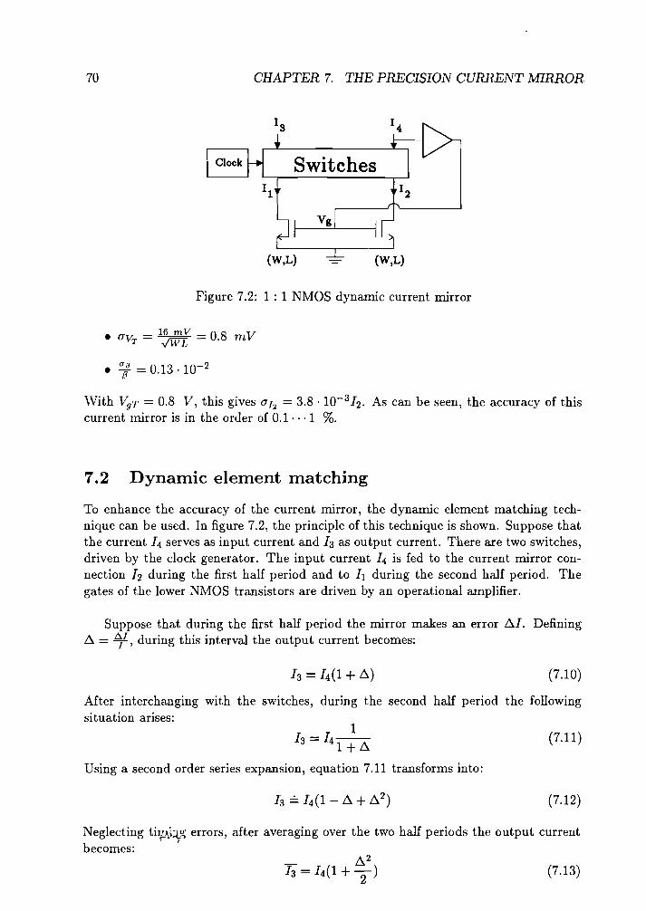
70 CHAPTER 7. THE PRECISION CURRENT MIRROR
Switches
Figure 7.2: 1 : 1 NMOS dynamic current mirror
16 mV a8 v• °VT = VWL = . m
• 0'; = 0.13.10-2
With VgT = 0.8 V, this gives 0h = 3.8 . 10-312 . As can be seen, the accuracy of thiscurrent mirror is in the order of 0.1 ... 1 %.
7.2 Dynamic element matching
To enhance the accuracy of the current mirror, the dynamic element matching technique can be used. In figure 7.2, the principle of this technique is shown. Suppose thatthe current 14 serves as input current and h as output current. There are two switches,driven by the clock generator. The input current 14 is fed to the current mirror connection h during the first half period and to h during the second half period. Thegates of the lower NMOS transistors are driven by an operational amplifier.
Suppose that during the first half period the mirror makes an error t:,.1. Definingt:,. = 'JI, during this interval the output current becomes:
(7.10)
After interchanging with the switches, during the second half period the followingsituation arises:
(7.11)
Using a second order series expansion, equation 7.11 transforms into:
(7.12)
Neglecting ti:r;\~~ errors, after averaging over the two half periods the output currentbecomes:
(7.13)
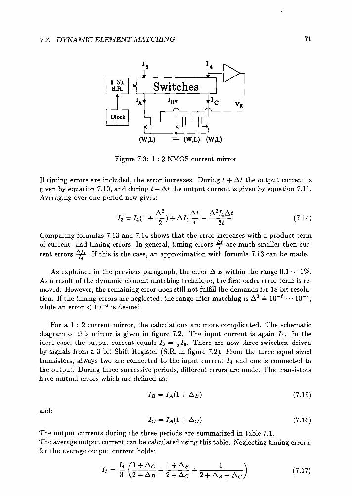
7.2. DYNAMIC ELEMENT MATCHING
Switches
Figure 7.3: 1 : 2 NMOS current mirror
71
If timing errors are included, the error increases. During t + ~t the output current isgiven by equation 7.10, and during t - ~t the output current is given by equation 7.1l.Averaging over one period now gives:
(7.14)
Comparing formulas 7.13 and 7.14 shows that the error increases with a product termof current- and timing errors. In general, timing errors ~t are much smaller then current errors ~. If this is the case, an approximation with formula 7.13 can be made.
As explaiued in the previous paragraph, the error ~ is within the range 0.1 " . 1%.As a result of the dynamic element matching technique, the first order error term is removed. However, the remaining error does still not fulfill the demands for 18 bit resolution. If the timing errors are neglected, the range after matching is ~2 == 10-6 ... 10-4 ,
while an error < 10-6 is desired.
For a 1 : 2 current mirror, the calculations are more complicated. The schematicdiagram of this mirror is given in figure 7.2. The input current is again 14 • In theideal case, the output current equals 13 = ~14' There are now three switches, drivenby signals from a 3 bit Shift Register (S.R. in figure 7.2). From the three equal sizedtransistors, always two are connected to the input current 14 and one is connected tothe output. During three successive periods, different errors are made. The transistorshave mutual errors which are defined as:
(7.15)
and:(7.16)
The output currents during the three periods are summarized in table 7.l.The average output current can be calculated using this table. Neglecting timing errors,for the average output current holds:
-1 14 (1 + ~c 1 + ~B 1 )3 = - + + ----,----
3 2 + ~B 2 + ~c 2 + ~B + ~c(7.17)

72 CHAPTER 7. THE PRECISION CURRENT MIRROR
I period I 13 connected to I 14 connected to I output current
1 A B,e I I l+~c3 = 42+~B
2 B A,e I I 1+~83 = 42+~c
3 e A,B h = 14 2+~~+~c
Table 7.1: Periods of the 1 : 2 dynamic current mirror
This equation can be transformed to:
1 + b.B + b.e + f2b.~ + f2b.b + f2b. Bb.e + ib.~b.e + ib.Bb.b + ib.~ + ib.&
1 + b.B + b.e + ib.~ + ib.b + ~b.Bb.e + ib.~b.e + ib.Bb.b(7.18)
To simplify the calculations, only the tenus contributing up to a second order error areincluded. Next, the approximation 1~:Z: ::::::: 1 - x + x 2 is used. This gives as final result:
(7.19)
Thus the error of the 1 : 2 dynamic current mirror is in the same order of magnitudeas with the 1 : 1 mirror, and therefore no 18 bit dynamic range can be achieved.
7.3 Enhancing the current mirror accuracy
From equation 7.19 it is clear that the solution to enhance the dynamic current mirroraccuracy is to improve the matching between the currents lA, IB and Ie. The errorsb.B and b.e are equal, they depend on the matching of the MOS transistors. Fromequation 7.19, the needed accuracy of 10-6 is reached when the matching errors b.B
and b.e are smaller then V2 . 10-6 = 1.4 . 10-3 .
When the matching errors b.B and b.e have standard deviations of (7 :::; 7 . 10-3 , thenthe matching of two transistor currents is within ±2(7 = ±1.4· 10-2 with a probabilityof 95.4 %, assuming a normal distribution of the errors. As explained in the previousparagraph, a matching of 7 . 10-3 is realizable.
Now an improvement with a factor ten is needed to reach the desired accuracy. Thisimprovement is easy to realize by using an array of equal transistors. For example, fora 1 : 1 mirror, n transistors can be used for the input current and n transistors forthe output transistor. The input and output transistors must be randomly alternatedwithin the array. This technique is known as the geometric averaging technique.

7.4. IMPLEMENTATION OF THE CURRENT MIRROR 73
With the same input current, the single transistor current is multiplied with a factorlin. The variance o} of the sum current is, according to the law of the central limit
2theorem, multiplied with a factor n. Thus, the resulting relative variance It of theoutput current is multiplied with a factor -{!1 = ~. If n is not too small, the accuracyT increases with the square root of the number of transistors in parallel. The factor10 improvement is reached for n = 100, resulting in a current mirror with a relativeoutput current error below 10-6 .
7.4 Implementation of the current mirror
The implementation of the 1 : 1 and 1 : 2 mirrors is basically the same. The 1 : 2 mirror requires more elements because of the extra 3 bit shift register and extra switchesneeded, but no extra problems with the implementation are expected. Therefore, onlysimulations with the 1 : 1 current mirror are presented, carried out with the schematicdiagram given in appendix C. In this schematic diagram, the following parts of theDAC are present:
• The MSB current source nm1, pm1 and rl, with cascode pm2;
• The dynamic 1 : 1 current mirror with:
PMOST differential pair, with Miller compensation capacitor ex;Mirror transistors nm4, nm5 and nm9;Switches nm2, nm3, nm6 and nm7;
• A second MSB current source, with separated transistor pm7 to be able to introduce a current error;
• The error detector with PMOST differential pair and bipolar diodes pm5 andpm6.
Transistor nm9 is added to have the possibility to introduce an error in the current mirror. The dynamic current mirror switches are operated at a switch frequencyIdem = 250 kHz, in practice this frequency can be enhanced up to 10 MHz. However,to analyze the error detector output, now a low switching frequency is used. In practice a high frequency must be used, to utilize the averaging property of the parasiticcapacitance of the bipolar diodes.
The combination of the PMOST differential pair and the mirror transistors nm4,nm5 and nm9, forms a two-stage configuration. To overcome instabilities during interchanging of the mirror transistors, the Miller capacitor ex is added.
Two types of simulations are executed. First, with 12 constant and an error inthe current mirror, the error detector output is analyzed. The simulation results areshown in figure 7.4. The feedback Opamp keeps the current source lower output (node1) at a constant voltage of 1 V. The error detector keeps the voltage at node 19 at

74 CHAPTER 7. THE PRECISION CURRENT MIRROR
Oct 16, Bn14:56:15
Dyn~c current m1rror1:1 CUrrent mirror aimulation eX-lOp; 11-22
(LIN)(LIN)- y1-axia
W(ll)
- y2-axia
I(P" 5\0)
I (PH 6\0)
1.8
1.4
1.2
1.0
800. om
600. om
400.om
II
P I(PM 5\ ) at y2-axia it I(PM 6\0) at y2-axi p\
7 I-'
IW(ll) at y1-axia / \
~
2.0u
1.5u
1.0u
500.0n
0.0
-500. On
-l.Ou
-1.5u0.0
l.Ou2.0u
3.0u
(LIN)
4.0u5.0u
or
Figure 7.4: Simulation result with the dynamic current mirror, 12 = II
1 V and absorbs the current difference between the output current of the dynamiccurrent mirror and the output current of the second MSB current source. By choosingII = 22 pm, an error of approximately 170 nA is introduced in the current mirror, thiserror current flows through the error detector bipolar diodes pm5 and pm6. The errordetector transforms the error current into the output voltage at node 11, this voltagecan be used to adjust the output current of the second current mirror.
The simulation results are as expected. The dynamic current mirror introduces noinstabili ties.
In the second simulation, a slowly raising ramp voltage, raise time irc = 10 ms,is applied to the gate of pm7, so 12 decreases approximately linearly. Meanwhile, thedynamic current mirror is operated at a switching frequency of Idem = 50 kHz. Nowthe detector output is analyzed. When the second current source output 12 crosses theMSB current value It, the detector output must alternate from low to high.The simulation result is shown in figure 7.4. Again, the results are in accordance withthe expectation. There is a little ripple at the voltage at node 11. This ripple hasa frequency of 50 kHz, and is due to the interchanging within the dynamic currentmirror. When the switching frequency of the dynamic current mirror Idem is enhanced,this ripple will decrease due to the feedback capacitance in the detector circuit.Besides, there is a little delay of about 500 flS between the crossing of II - h andthe swapping of the detector output voltage. This delay is caused by the feedbackcapacitance of the detector. When the gate voltage of the current source transistorpm7 is changed in discrete steps, and a wait-time is introduced between these steps,the detector output level will be in accordance with it's input current.

7.4. IMPLEMENTATION OF THE CURRENT MIRROR 75
Oct 21, 199111:28:29
Dynamic current c~1~rat1on
D_tector output
(LIlli) SOOIll act1V18 (LIlli)
- yl-axi.
WIll)
- y2-axio
I(R 1)
I(R 2)
2.2
2.0
1.8
1.'
1.4
1.2
1.0
800.010
'00.010
"-~~
""WIll)-
~ 7 I(~l)
..........,I '"I ~ I (R_2)
/ ~.-/ "-......
505.Ou
504.95u
504. tv
504.85u
504.8u
504.75u
504.7u
504.'5u
504. 'U400.010
0.02.Om
4.010'.010
8.010
(LIlli)
10.Om
504.55u12.010
r
Figure 7.5: Simulation result with the dynamic current mirror, I(R2 ) decreasing

Chapter 8
Glitches due to switching
At the analog converter output, glitches exist due to switching in the converter. Twodifferent glitch error sources can be distinguished:
• Glitch errors due to switching in the precision current mirrors, the dynamic element matching technique;
• Glitch errors due to switching of the bit currents.
Each of these error sources will be analyzed.
8.1 Switching in the precision current mirrors
The dynamic element matching technique introduces switching transients at the precision current mirror output. These transient signals can disturb the output current ofthe bit current sources. The error in the output current, due to the dynamic elementswitching technique, must be less then the LSB current hSB = 3.9 nA. The PMOScascode transistor of the bit current source shields this current source from the dynamic current mirror. In order to minimize the error, the bulk of this PMOS cascodetransistor is connected to the supply voltage Vdd . Now the capacitive feedthrough ofthe switching signal is minimized.The switches from the dynamic element switching technique are designed to have amaximal voltage drop of 50 mV with minimal dimensions. The switches are operatedwith a gate voltage of 0 or 5 V. Simulation results of the glitch error will be analyzedin the next paragraph.
8.2 Switching the bit currents
The digital input code controls the switches, switching the output current to one of theI IV converters. In order to minimize these glitches, all the switches must be operatedsimultaneous when a new input code is present. Besides, some precautions must betaken to keep the glitch energy smaller then half the LSB energy.With an input frequency of 200 kHz and an output voltage range of 1 V, the LSBenergy becomes 2-18 V· 5 /is = 19 pVs. Thus, after switching of the input code, the

8.2. SWITCHING THE BIT CURRENTS 77
vur
:+. 6275
~I
pula.(5,O,tb,tr,th,tr,per)
10
... Wt1-256,LU-1.5,HOLT-lWD-256,LU-l.5,MOLT-l
11
¥'WO-12,LO-1O,MOLT-256
3 13
:+;7~ :+._4 p :+._5• 24724
- - - -pula.(O,5,tb,tr,th,tr,per)
WU-7.25, LO-12, HULT-256
~:+ 9
18 .-r 5178k -=-
pulse (0, 5,tbb,tr,thb,tr,perb) L---+-~ pulae(5,O,tbb,tr,thb,tr,perb)
WO=100,LO-l.5,MULT=1WU-100,LO-l.5,MOLT-l
Figure 8.1: Schematic diagram for glitch error analysis
remaining glitch error must be smaller then 10 pVs. The glitch energy is minimizedby scaling the switches of the bit currents, conform the current flowing through theswitch. The switches are designed to have a maximal voltage drop of 50 m V withminimal dimensions. The schematic diagram of figure 8.1 is used to analyze the glitcherrors introduced by both the bit current switches and the dynamic element switching.The sit\lation simulated by figure 8.1 equals the MSB transition. The following parts
of the DAC are included in this diagram:
• The MSB current source nml, r1 , pm1 with cascode pm4;
• The bit current switches pm5 and pm6;
• The I IV converter, implemented as folded cascode Opamp;
• The switches from the dynamic element matching nm2 and nm3.
Further reduction of the glitches is obtained by using a deglitching capacitor Cp III
parallel with the Opamp feedback resistor Rf. With Cp = 15 pF and Rf = 1 kn, this
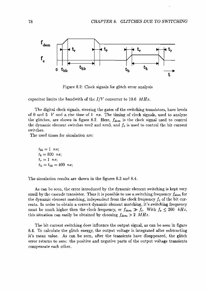
78 CHAPTER 8. GLITCHES DUE TO SWITCHING
-------+t
Figure 8.2: Clock signals for glitch error analysis
capacitor limits the bandwith of the flV converter to 10.6 MHz.
The digital clock signals, steering the gates of the switching transistors, have levelsof 0 and 5 V and a rise time of 1 ns. The timing of clock signals, used to analyzethe glitches, are shown in figure 8.2. Here, idem is the clock signal used to controlthe dynamic element switches nm2 and nm3, and ie is used to control the bit currentswitches.The used times for simulation are:
tbb = 1 ns;tb = 800 ns;tr = 1 ns;th = thb = 400 ns;
The simulation results are shown in the figures 8.3 and 8.4.
As can be seen, the error introduced by the dynamic element switching is kept verysmall by the cascode transistor. Thus it is possible to use a switching frequency idem forthe dynamic element matching, independent from the clock frequency ie of the bit currents. In order to obtain a correct dynamic element matching, it's switching frequencymust be much higher then the clock frequency, or idem ~ ie. With ie ~ 200 kHz,this situation can easily be obtained by choosing idem> 2 MHz.
The bit current switching does influence the output signal, as can be seen in figure8.4. To calculate the glitch energy, the output voltage is integrated after subtractingit's mean value. As can be seen, after the transients have disappeared, the glitcherror returns to zero: the positive and negative parts of the output voltage transientscompensate each other.

8.2. SWITCffiNG THE BIT CURRENTS 79
OCt 15, 199114:31:10
Dynamic element awitchingBit currant error
(LIN) zoom active- y1-ax!a -
I(1l. 1)
504.687\1
504.686u ....... "
504.685u0.0 200.0n 400.0n 600.0n 800.0n
100.0n 300.0n 500.0n 700.0n
(LIN) 'l!
Figure 8.3: Dynamic element switching glitch error
Oct 15, 199114 :35:50
MsB current ••itChingOutput glitch error GLI-ITG (VII(VUIl.)-3. 70465, 800N)
(LIN) 100111 active (LIN)
0.0
30.0p
40.0p
20.0p
10.Op
-10.0p
-30.0p
-50.0p
-ZO.Op
-40.0p
LOu
T
975.0n950.0n
(LIN)
925.0n900.0n
875.0n850.0n
825.0n800.0n
/...-
VI
1V
lfV
3.8
3.7
3.84
3.86
3.82
3.76
3.78
3.72
3.68775.0n
3.74
- y2-axis -
- y1-axb
VII (VOR)
GLI
Figure 8.4: Bit current switching glitch error

Chapter 9
Conclusions
A system setup for an 18 bit CMOS Digital to Analog Converter has been presented.To reach 18 bit accuracy, a calibration technique is used. The 10 bit range of a passivecurrent divider is extended to 18 bit by adding calibrated current sources. The calibration technique requires a very high precision current mirror. The accuracies that canbe obtained with different current mirror configurations are:
• A standard current mirror, as shown in figure ref, has an accuracy of 10-2•
• The standard current mirror can be extended with an interchanging network.In this way, applying the dynamic element matching technique, the accuracy isenhanced up to 10-4 •
• In stead of using a two-transistor dynamic current mirror, an array of 2n equaltransistors can be used. The transistors must be randomly interconnected, usinghalf of the transistors for the input and half of the transistors for the output. Thistechnique is called the geometric averaging technique. The matching between inand output current is improved with a factor ~.
• Combining the dynamic element matching technique with the geometric averagingtechnique, the resulting accuracy is 10-6 for n = 100.
The dynamic element matching uses time averaging to cancel errors in first order. Thetime averaging property requires a capacitor. By using a high switching frequency, thiscapacitor can be integrated on chip, so a DAC without external components results.
To calibrate the bit currents, an inherently monotonic resistive divider is presented.An error detector with a 1 nA sensitivity detects the difference between the actual bitcurrent value and the desired value.
It is shown that no problems arise in designing an output I IV converter with 18bit dynamic range.
By biasing the bit current source transistors temperature independent, the DACoutput voltage is stabilized for temperature variations. The bias voltages are derivedfrom a reference voltage generator.

81
Translating the traditional bipolar bandgap reference source into a CMOS schematicdiagram gives a setup, practically insensitive for supply voltage variations. For temperature variations, the source is compensated by adding a bipolar diode. The extradegree of freedom that now arises, is used to optimize the temperature behaviour ofthe reference source.

Bibliography
[1] van de PLASSCHE, R.J., Current source arrangement having a prectSwncurrent-mirror circuit, United States Patent number 4,573,005, Date of patentFeb. 25, 1986.
[2] GREGORIAN, R, and G.C. Temes, Analog MOS Integrated Circuits for signalprocessing, John Wiley & Sons, New York, 1986.
[3] SZE, S.M., Semiconductor devices, Physics and Technology, John Wiley & Sons,New York, 1985.
[4] SCHOUWENAARS, H.J., et al., A Low-Power Stereo 16-bit CMOS D/A Converter for Digital Audio, IEEE J. Solid-State Circuits, Vol. 23, No.6, December1988.
[5] PELGROM, M.J.M., et al., Matching Properties of MOS Transistors, IEEE J.Solid-State Circuits, Vol. 24, No.5, December 1989.
[6] GRAAFF, H.C., de and F.M Klaassen, Compact Transistor Modelling for CircuitDesign, Springer-Verlag, Wien, 1990.
[7] van de PLASSCHE, R.J., High speed and high resolution analog-to-digital anddigital-lo-analog converters, Eindhoven Druk B.V., Eindhoven, 1989.

Appendix A
Current source transistorparameters
MOSCA version 3.0Today is 16-AUG-1991 and the time is 8:26:31Last program update November 1, 1989Last process parameter update: 11 april 1991 3.00
ANALYSIS 1; PROCESS: C200 special for group Wouda, go correctedT=27.00 ; N-MOST ; "typical"-case
-- input parameters ------------------------------------------------------channel ; case ; Wlay ; Llay ; Ids ; Vds ; Vsb ;== dimensions ============================================================Weff = 12.10E-06 Wlay = 12.000E-06Leff = 9.760E-06 Llay = 10.000E-06-- bias point (abs. values) saturated; normal drain current ---------Vgs = 1.688E+00 Vgt = 0.201E+00 Ids = 1.953E-06Vsb = 2.550E+00 Vdss = 0.181E+00 Vds = 0.600E+00
-- trans conductances -----------------------------------------------------gm = 19.39E-06 go = 8.442E-09 gmb = 3.658E-06-- eq. input noise (sqrt(sff) at 1kHz) ----------------------------------SQRT(Sff) = 87.23E-09 SQRT(Sfw) = 33.34E-09 Fknee = 6.847E+03
-- capacitances ----------------------------------------------------------Cox = 203.9E-15 Cgs(sat). 135.9E-15 Cgd • 3.751E-15Cdb = 23.47E-15 Cpocsub = 0.0
-- other parameters ------------------------------------------------------Vto = 0.819E+00 Vts = 1.487E+00 Vt = 1.487E+00Kfactor = 0.491E+00 KOfactor = 0.680E+00 Boc = 77.85E-06thetaa = 74.56E-03 delta = 0.114E+00 twophi = 0.650E+00thetab = 44.89E-03 shift = 1000.0E-09 Nfactor = 1.000E+00thetac = 1000.0E-09 gamma = 2.160E-03 Pfactor = 0.0-- standard deviation offset voltage ------------------------------------sd(Vt) = 1.223E-03 sd(Beta) = 185.0E-09 sd(Vgs) = 1.238E-03======================== *** MOSCA mode 2 *** =========================

86 APPENDIX A. CURRENT SOURCE TRANSISTOR PARAMETERS
ANALYSIS 2; PROCESS: C200 special for group Wouda, go correctedT= 27.00 ; P-MOST ; "typical"-case-- input parameters ------------------------------------------------------channel ; case ; Wlay ; Llay ; Ids ; Vds ; Vsb ;== dimensions ============================================================Weff = 7.150E-06 Wlay = 7.2500E-06Leff = 11.92E-06 Llay = 12.000E-06-- bias point (abs. values) saturated; normal drain current ---------Vgs = 1.704E+00 Vgt = 0.538E+00 Ids = 1.953E-06Vsb = 0.250E+00 Vdss = 0.448E+00 Vds = 0.700E+00
trans conductances -----------------------------------------------------gm = 7.052E-06 go = 15.32E-09 gmb = 2.386E-06
eq. input noise (sqrt(sff) at 1kHz) ----------------------------------SQRT(Sff) = 17.11E-09 SQRT(Sfw) = 55.28E-09 Fknee = 95.86E+00-- capacitances ----------------------------------------------------------Cox = 147.2E-15 Cgs(sat) = 98.10E-15 Cgd = 2.145E-15Cdb = 24.14E-15 Cpocsub = 162.7E-15-- other parameters ------------------------------------------------------Vto = 1.078E+00 Vts = 1.168E+00 Vt = 1.168E+00Kfactor = 0.632E+00 KOfactor = 0.632E+00 Boc = 22.50E-06thetaa = 0.168E+00 delta = 0.200E+00 twophi = 0.650E+00thetab = 0.296E+00 shift = 1000.0E-09 Nfactor = 1.000E+00thetac = 1000.0E-09 gamma = 3.933E-03 Pfactor = 0.550E+00-- standard deviation offset voltage ------------------------------------sd(Vt) = 1.437E-03 sd(Beta) = 30.39E-09 sd(Vgs) = 1.559E-03======================== *** MOSCA mode 2 *** =========================

Appendix B
Folded cascode schematicdiagram

0000
WO-SOO, LO-3, MOLT-l WO-SOO, LO-3, MOLT-l WO-400, LO-S , MOLT-l
IllD_13
WO-l00, LO-20, MOLT-I
IllD 14
WO-40, LO-l0,HOLT-l
WO-600,LO-20,MOLT-l
~12
pm_I vm
e 2volas
-
WO-600,LO-20,MOLT-l
14
vol13
c 2
pm 20
WO-1S00,Lo-l0,MOLT-l
vo2
WO-300,LO-l.S,MOLT-l WO-300,LO-l.5,MOLT-l WO-600,LO-S,HOLT-l WO-l00,LO-S,MOLT-l 16 WO-400,LO-S,MOLT-l
WO-1S00, LO-l.5,HOL~~T:-~1---+====:;:::=====;::::=========::::;:==+- ---1r--__~~~__.......__....,

Appendix C
Current mirror schematicdiagram

WU-12, LU-lO,MULT-256 WO-12, LU-lO, MULT-256 20
vdd
100,5,100,5, 79k, 50, 5
,to. 7371
WO-lOO, LO-l ~5,HOLT-l
• 12":"5
1fO-20, LtJ-20 ,KULT-128
WO-lOO, LO-l. 5,MULT-l
17
WU-13~5,LtJ-4,MULT-256
2
11-----I1l--to---- -+I--""'--=--4-----------------l 5""'_5
W-20,LO-20,MULT-l21
WU-13 ~ 5, LtJ-4, KJLT-256
.5pGJ....(5, 0, tb, t:r,t:h,t:r,per)
tm-lOO,LO-l.5, MULT-l
••piiJ.•• (O,5,tb, t:r,t:h, t:r,per)WIJ-lOO, LtJ-l ~ 5, HOLT-l
8."1"1o"1