eindhoven university of technology master new high … u / e technische universiteit eindhoven...
TRANSCRIPT

Eindhoven University of Technology
MASTER
New high-speed all-digital phase-locked loop and bit detector for optical recording
van Beurden, N.J.H.M.
Award date:2003
DisclaimerThis document contains a student thesis (bachelor's or master's), as authored by a student at Eindhoven University of Technology. Studenttheses are made available in the TU/e repository upon obtaining the required degree. The grade received is not published on the documentas presented in the repository. The required complexity or quality of research of student theses may vary by program, and the requiredminimum study period may vary in duration.
General rightsCopyright and moral rights for the publications made accessible in the public portal are retained by the authors and/or other copyright ownersand it is a condition of accessing publications that users recognise and abide by the legal requirements associated with these rights.
• Users may download and print one copy of any publication from the public portal for the purpose of private study or research. • You may not further distribute the material or use it for any profit-making activity or commercial gain
Take down policyIf you believe that this document breaches copyright please contact us providing details, and we will remove access to the work immediatelyand investigate your claim.
Download date: 26. Jun. 2018

T U / e technische universiteit eindhoven
Section of Infonnation and Communication Systems (ICS/CNDIES) Faculty of Electrical Engineering ICS/CNDIES 819
Master's Thesis
Coaches:
Supervisor: Date:
New High-Speed All-Digital Phase-Locked Loop and Bit Detector
for Optical Recording
N.J.H.M. van Beurden
lng. J.A.H.M. Kahlman (Philips Research Eindhoven) Ir. A.H.J. Irnmink (Philips Research Eindhoven) Prof.ir. M.P.J. Stevens June 2003
The Faculty of Electrical Engineering of the Eindhoven University of Technology does not accept any responsibility regarding the contents of Master's Theses

ew High-Speed All-Digital Phase-Locked Loop
And Bit Detector For Optica Recording
Master's Thesis
N.J.H.M. van Beurden

New High-Speed All-Digital Phase-Locked oop
And Bit Detector For tic IRe rding
Master's Thesis
Personal Data: Ing. N.j.H.M. van Beurden
Student number: 494708 (ITW-VKO-VT) beurden~email.com
In Cooperation With: Ing. AJ.A Rutten
Research Group: Information & Communication Systems (I.C.S.)
Chair: Computers, Networks & Design (CN.D.)
Prof. Ir. M.P.j. Stevens
Company: Philips Research (High-Tech Campus)
Hightech Campus Prof. Holstlaan 4
5656 AA Eindhoven
Supervisor Eindhoven University of Technology: Prof. Ir. M.P.j. Stevens
Company Supervisors: Ing. j.AH.M. Kahlman (Main Supervisor) Ir. AH.J. Immink (Secondary Supervisor)
Graduation Period: 2 September 2002 till 17 june 2003
Version: 1.1
I CONFIDENTIAL I
© All rights reserved. Reproduction or cataloging, in whatever way, of this publication in whole or in part is prohibited without the written consent of the author.

Ter nagedachtenis van: In memory of:
t N.J. van Beurden t A.M.J. van Beurden-Bax
"Age quod agis ... velie est posse."

Preface
Preface
Consummatum est, after many days of hard labor and problem solving here my master's thesis 1 lays before you. This graduation assignment concludes my study at the Eindhoven University of Technology and was carried out at Philips Research Laboratories Eindhoven (at the Philips HighTech Campus). It has been a very challenging and instructive time.
This master's thesis is divided into two parts. The first part, comprising chapters 1, 2. 3 and 4 deals with the conventional concept ADPLL and contains some general theory about PLLs and bit detection. The second part, comprising chapters 5 and 6 deals with the new concept ADPLL and bit detector. Chapter 7 contains the conclusions.
The first chapter gives a short introduction to optical media and the graduation assignment is described. It gives a general overview of an optical disc system and shows how the electrical signals are generated. Also, the assignment, goals, task partitioning and the report structure are discussed.
Acknowledgements
I would like to take the opportunity to acknowledge some people for their contribution. First of all, I want to thank Robert Rutten for all the fun we had fulfilling our graduation assignment. It was a very pleasant collaboration. This wonderful graduation opportunity would never have been possible without the help of Rob Otte. He arranged the first contacts for our assignment and we both owe him a lot of gratitude. Our supervisors at Philips, Joost Kahlman and Andre Immink, learned us a lot of important things. The bets we had for beer I will never forget, both you and we have lost some bottles. Also, thanks goes out to Kees Schep and all the other group members of the Storage Signal Processing group at Philips Research Laboratories Eindhoven, who gave us the opportunity to work within their environment.
Thanks to Professor Mario Stevens for gUiding us through our graduation period. The discussions we had with you at your home were very pleasant. We thank you for your help and hospitality. I also would like to thank Professor Jan Bergmans for his time, interest and support.
Of course, my acknowledgements go out to all the people who guided me through my study years. My mom, dad, brother, family and my friends had a lot of patience and understanding over the years.
Finally, my greatest respect goes out to my beloved grandmother Miet van Beurden-Bax who died during my graduation period. I wish she could still be here to see me finish it. I know she would be very proud, just like my grandfather Nico van Beurden would be. Unfortunately, I never knew him. He worked for Philips with great pride, for all of his too short life. To these persons I dedicate this thesis ... as I personally promised.
N.J.H.M. van Beurden Eindhoven, 16 June 2003
document is typeset with ~E><. most of the drawings are made with aid of the drawing program LaTeXPiX which is developed by the author.
N.J.H.M. van Beurden 16 june 2003
Summary III
Summary
Phase-Locked Loops (PLL) are used in almost every data processing system. One application for the PLL is as a clock regenerator. Here, the PLL has to produce a signal with a phase and frequency that is ideally equal to the incoming signal so that the sampling moments of the, initially unsynchronised, signal can be determined. The past few years there is a trend towards so-called All-Digital Phase-Locked Loops. These ADPLLs completely consist of digital circuitry and have some benefits over analogue or mixed-signal PLLs.
In optical disc systems like the Compact Disc (CD), Digital Versatile Disc (DVD), the forthcoming Blu-ray Disc and next generations ever increasing bit rates are observed. Here, data is read from an optical disc, retrieving a high-frequency analogue signal. Digital processing has to be carried out on this high-frequency signal so the stored binary information can be retrieved. The processing in general consists of analogue preprocessing, analogue-to-digital conversion and a number of digital processing blocks, including an ADPLL and bit detector.
In the conventional concept, the first building blocks of the data recovery circuitry use a relatively high clock frequency and (most of the time) process only a single bit per clock cycle. The remaining blocks are connected to clocks that have a relatively lower frequency because those blocks do operations on multiple bits at once.
The bottleneck of the present concept lays within the first blocks of the path that run on the higher clocks, being the equaliser, analogue-to-digital convertor, ADPLL and bit detector. When shifting to higher bit rates the clock of those blocks has to be increased accordingly. They are reaching their processing limits, making the implementation more critical and expensive.
Possible solutions to the facing problems were found and patented [7]. Amongst others, a new architecture for the ADPLL and bit detector has been developed. These blocks now output bits in a parallel manner so the clock frequency is lowered accordingly.
The goal of the aSSignment was to model, simulate and implement a prototype ADPLL and bit detector, following the conventional and new concept, so they can be compared and the feasibility of the new concept is shown. Theory, benefits and drawbacks, faced problems and their solutions will be discussed in this master's thesis.
N.J.H.M. van Beurden 16 June 2003

Samenvatting v
Samenvatting
Phase-Locked Loops (PLL) worden in nagenoeg elk gegevens verwerkend systeem gebruikt. Een toepassing van de PLL is als klok regenerator. Hier moet de PLL een signaal genereren waarvan de fase en frequency in het ideale geval gelijk zijn aan het inkomendesignaal zodat de bemonstermomenten van het, initieel ongesynchroniseerde, signaal kunnen worden bepaald. De afgelopen jaren is er een trend waar te nemen naar zogenaamde All-Digital Phase-Locked Loops. Deze ADPLLs bestaan compleet uit digitale circuits en hebben een aantal voordelen ten opzichte van analoge of mixed-signal PLLs.
In optische plaat systemen zoals de Compact Disc (CD), Digital Versatile Disc (DVD), de verwachte Blu-ray Disc en volgende generaties worden almaar toenemende bit rates waargenomen. Hier wordt data gelezen van een optische plaat zodat een hoog frequent analoog signaal verkregen wordt. Digitale bewerking moet op dit hoog-frequente signaal worden toegepast om de opgesJagen binaire informatie terug te kunnen winnen. De bewerkingen bestaan over het algemeen uit analoge voorbewerking, analoog naar digitaal omzetting en uit een aantal digitale signaalbewerkingsblokken, waaronder de ADPLL en bit detector.
In het conventionele concept gebruiken de eerste bouwblokken van het data terugwinnende circuit een relatief hoge klok frequentie en (meestal) bewerken ze per klokcyclus slechts een bit informatie. De overige bouwbiokken zijn verbonden met klokken met een relatief lagere frequentie omdat deze blokken operaties uitvoeren op meerdere bits tegelijkertijd.
Het knelpunt van hethuidige concept zit in de eerste bouwblokken van het pad die op de hoge klok werken, namelijk de equaliser, analoog naar digitaal omzetter, ADPLL en bit detector. Ais er naar hogere bit rates gegaan wordt zal de klok van deze blokken evenredig stijgen. De maximale verwerkingscapaciteit wordt bereikt zodat de implementatie kritischer en duurder wordt.
Mogelijke oplossingen voor de komende problemen werden gevonden en gepatenteerd [7]. Onder andere, is er een nieuwe architectuur voor de ADPLL en bit detector ontworpen. Deze blokken bewerken nu bits op een parallele manier zodat de klokfrequentie evenredig verlaagd wordt.
Het doeJ van de opdracht was de modellering, simulatie en implementatie van een prototype ADPLL en bit detector, volgens het conventionele en nieuwe concept, zodat deze vergeleken kunnen worden en de correcte werking van het nieuwe concept bewezen werd. Theorie, voordelen en nadelen. gevonden problemen en oplossingen zullen worden besproken in dit verslag.
N.J.H.M. van Beurden 16 June 2003

Table Of Contents VII
Table Of Contents
Chapter 1: Introduction 1 1.1 Fundamentals Of Optical Disc Systems
1.1.1 Brief Introduction 1.1.2 Group: Storage Signal Processing ... .. _ .. _ .. _. ___ ._ ..... _._ ........ _.' __ ........ __ .. " ._,, ___ .. ,._. 4
4 4 5 5 6 7
1.2 Graduation Assignment 1.2.1 Problem Situation
1.2.2 1.2.3 1.2.4 1.2.5
Assignment And Goals Methods Of Problem Solving And Research Task Partitioning Report Structure
Chapter 2: Phase-Locked Loop Basics 2.1 First Observations 2.2 Mathematical And Control Systems Analysis
2.2.1 Phase Detector 2.2.2 Loop Filter 2,2.3 Controlled Oscillator 2.2.4 PLL Laplace Domain Model
2.3 Classifications
Chapter 3: Experimental Environment 3.1 Hardware
3.1.1 JUB Rack 3.1.2 Generic II 3.1.3 AID Convertor And DIA Convertor Extension Cards
3.2 Firmware 3.3 Software
3.3.1 Control Software Platform 3.3.2 Programming Flow 3.3.3 Parameter Editor
Chapter 4: Conventional Concept ADPLL Implementation 4.1 Firmware Implementation
4.1.1 Phase Detector
9 9
10 10 11 11 12 12
1S 15 15 16 17 17 18 18 19 20
23 23 24
4.1.2 Loop Filter_ .. ,, __ ., .. " ...... ,"'_, ... , .. , __ .. " .... , .... ,._".",._ .. , __ " ...... _ ............. ,...... 26 4.1.3 Nominal Frequency 4.1.4 DTO 4.1.5 Bit Detection
4.2 Control Software Implementation 4.3 Results
Chapter S: New Concept ADPLL & Bit Detection 5.1 Architecture
5.1.1 Equaliser 5.2 Slicer
N.j.H.M. van Beurden
27 28 28 30 31
3S 35 36 36
16 june 2003
VIII
5.3 Shift Register 5.4 Mixer 5.5 Clock Divider 5.6 AID Convertor
Table Of Contents
36 36 39 39
5.7 All-Digital Phase-Locked Loop ~_""._".",_,"~.,,",_~" __ "_~_~ .. ~_ .. _._ •. __ ."_, _________ ,~.~"""'_._""., __ " __ ._, __ . ___ ,._""",._. 39
5.7.1 Phase Detector 5.7.2 Loop Filter 5.7.3 DTO
5.8 Bit Decision Unit 5.8.1 Single DTO Method 5.8.2 Multiple DTO Method
5.9 Multiple Clock-Phase All-Digital Phase-Locked Loop 5.10 Multiple Shift Registers 5.11 Dual Shift Registers
Chapter 6: New Concept Modelling & Simulation 6.1 Modelling
6.1.1 Signal Generation 6.1.2 Slicer & Shift Register 6.1.3 Mixer 6.1.4 AID Convertor 6.1.5 New Concept ADPLL 6.1.6 Bit Decision Unit
6.2 Implementation Problems & Solutions 6.2.1 Problems 6.2.2 Possible Solutions
6.3 Experimental Results 6.3.1 Phase Step Response 6.3.2 Frequency Step Response 6.3.3 Mixer 6.3.4 ADPLL 6.3.5 Multiple Clock-Phase ADPLL
6.4 ADPLL Key Parameters 6.4.1 Hold Range 6.4.2 Lock Range 6.4.3 Pull-In Range 6.4.4 Pull-Out Range
6.5 linear Phase
Chapter 7: Conclusions 7.1 Results 7.2 Recommendations
Bibliography
Appendix A: New Concept ADPLL System Calculations A.1 Overshoot A.2 Settling Time
16 June 2003
40 40 40 40 41 41 43 44 45
47 47 48 49 49 49 49 49 50 50 50 51 51 52 53 57 58 58 59 59 59 59 59
61 61 61
63
65 66 70
N.J.H.M. van Beurden

Table Of Contents
Appendix B: New Concept Mixer Transfer Functions & Differential Equations B.1 Summator/lntegrator B.2 Filter B.3 Gain & Offset
Appendix C: New Concept Mixer Calculations C.1 Bessel-Thomson C.2 Delay Equalisation
List Of Figures
Glossary
Curriculum Vitae
N.J.H.M. van Beurden
IX
73 73 74 74
75 77 82
85
87
91
16 June 2003

1. Introduction
Chapter 1:
Introduction
Optical disc systems are complex systems containing a lot of state-of-the-art techniques. This first chapter will give a general introduction to the top level system and also focusses on the contents of the graduation assignment.
1.1 Fundamentals Of Optical Disc Systems
The following subsection will give a brief introduction to optical disc systems, intended for readers not (very) familiar with this topic. Next, the research group where the graduation assignment is carried out will be described. The purpose of this section can be seen as a preparation to the graduation assignment description. The text is based on [13], [18] and [19].
1.1.1 Brief Introduction
Optical media like the Compact Disc (CD), Digital Versatile Disc (DVD). Blu-ray Disc (BD) and forthcoming next generation standards are transparent plastic (polycarbonate) discs carrying a continuous spiral of impressed pits. The impressed surface is covered with a thin metallic layer on which one or more plastic layers are being used for protection (see figure 1.1 for a stylistic view of the different types of optical disc systems with their corresponding wavelengths (,X), Numerical Apertures (NA) and substrate dimensions).
NA=0.45 A ,-----
1.2mm substrate 0.6mm substrate 0.1 mm substrate
a: CD b:DVD c: Blu-ray Disc
Figure 1.1: Schematic diagrams of CD. DVD and Blu-ray Disc systems
The laser reads the profiled surface, perceiving the impressed pits and bumps by detecting the reflected light from the metallic coat. The data is read-out through the substrate layer so dust and scratches on the disc surface are averaged out over the relatively large area of the non-focussed beam.
An optical disc system can be considered as a transmission channel for the carried signal. A digital convention was agreed upon such that the light reflected by lands (positive peaks in the output signal of the photo detector) will be denoted by a digital "1 ". Conversely, the light reflected by pits (negative peaks in the output signal of the photo detector) will bear the digital "0" notation. But the same information will be available when the convention is reversed (so when a land equals a digital "0" and a pit equals a digital "1"). for only the length of the pits and lands is of importance. This is due to the used Non-Return to Zero
N.J.H.M. van Beurden 16 June 2003

2 1. Introduction
Inverted (NRZI) encoding during the mastering or recording of the disc.
When choosing the right geometrical depth of the pits, the light reflected by a pit will have approximately the opposite phase compared to the incident laser beam. This gives rise to destructive interference, limiting therefore the amount of light coming back from the pits. On the other hand any area surrounding a pit, which is usually called a land, does not produce destructive interference and will consequently look brighter. The resulting structure on the disc will cause diffraction of the laser light which leads to modulation of the amount of light on the photo detector. By reading the intensity of the reflected light it will therefore be possible to detect the disc internal structure and to recover the recorded information. The reflected main spot falls onto the central arrangement of photo detectors. By gathering the information received by all central detectors a High~Frequency (HF) signal modulated by the disc relief structure can be derived.
The data present on most optical disc standards is coded by a so-called Run-Length Limited code (RLL code). This code limits the lowest and highest transition frequency. For the data stream this means that bursts containing only zeros or bursts containing only ones are limited by a minimum and maximum length. The minimum limit is needed to reduce Inter-Symbol Interference (lSI) caused by adjacent pits. The maximum limit is needed for synchronisation purposes. More information on the RLL code can be found in section 3.1.1 of [14] and also extensive information can be found in [18].
The data recovery circuitry reconstructs the data stream, which is contaminated with noise, based on several general concepts. The building blocks present in an audio CD system are depicted in figure 1.2. The clock frequencies for the shown building blocks are not equal.
DC Offs(;tt Correction
Reflected light
Output Left
Output Right
elk3
Figure 1.2: Embodiment of a audio CD data recovery circuit
After detecting the reflected light with a photodetector1 ("PH" in figure 1.2) and amplification with a factor "G", the analogue HF signal is converted to a digital signal by an Analogue-to-Digital (AID) convertor (see [12] for more information). This AID convertor runs at a fixed system clock elk.
1 A photo detector consists of a photodiode followed by a current-to-voltage convertor.
16 June 2003 N.J.H.M. van Beurden

1. Introduction 3
The digitised signal is subsequently passed to a channel equaliser. This equaliser compensates the Modulation Transfer Function (MTF). Due to the limited resolving power of the objective lens a lowpass character is obtained. Some optical compensation methods have been proposed but electronic compensation is much cheaper and effective. The equaliser compensates for this low-pass behavior by boosting the high-frequency components of the signal. The equaliser is depicted in figure 1.2 as the block "EQ". The equaliser can also consist of analogue circuitry and is then placed just before the AID convertor. This is done in order to increase the effective dynamic range of the AID convertor for the shortest runlength.
After equalisation a Direct Current (DC) offset correction takes place, consisting of a so-called Threshold Detector (TD) and a Running Digital Sum (RDS). The threshold detector determines the points where the signal intersects a certain threshold level (also called slicing level). In all current optical media the channel code is DC free and hence. the intersection points are often called zero-crossings. The RDS block dynamically calculates the DC value of the signal. Its output is supplied to the threshold detector, represented as "TD" in figure 1.2.
The following dedicated circuit encountered in the optical disc communication channel is the Phase-Locked Loop (PLL). The task of the PLL is to regenerate the clock from the transmitted signal. This clock can subsequently be used to reconstruct the transmitted stream of digital symbols. Also, the regenerated clock serves as a time base for further signal processing (being the bit detector and the NRZ encoder in figure 1.2). It will only be possible to unambiguously determine a transmitted one or zero if a clock signal indicates the exact position in time of any transmitted bit. Usually. no separate clock channel is used in digital communications but the time base is embedded into the carried signal. The clock has to be regenerated, having a very precise phase and frequency relationship with respect to the incoming HF pulses. In optical disc systems, the PLL has become a standard solution for clock recovery .
. With the discussed building blocks the channel bits can be extracted from the HF signal by the bit detector (denoted as "Bit Det" in figure 1,2). After the bits. have been detected they are put through a so-called Non-Return to Zero (NRZ) encoder. When mastering or recording the disc, the signal level is high at a digital one and low at a digital zero. The resulting signal is converted to Non-Return to Zero Inverted (NRZI). This means that the signal is inverted at the center of each digital one. As discussed earlier. this lets length of the pits and lands (Le. the run length) be important instead of the convention used for the reflected light. Moreover. it gives the waveform fewer transitions thus simplifying the pit structure on the disc. At the decoding stage this code is reversed from NRZI to NRZ by the NRZ encoder/NRZI decoder.
When recording or mastering the CD. each 8 bits from the CIRC encoder are translated into 14 bits with the aid of Eight-to Fourteen Modulation (EFM) which specifies that the code words may not violate the runlength constraint of the code. Three merging bits are added to the resulting 14 bits. This is to prevent runlength violations when concatenating the code words and for suppressing DC. Hence, EFM is a DC free channel code. The EFM code has to be demodulated at the receiving end of the system, so that the channel bits from the optical disc are converted to data bits. Every 14 bit word (the 3 stuffing bits are thrown away) again becomes 8 bits. Depending on the design, EFM demodulation is done either by logic circuitry or a lookup table. Every channel word is converted to a data word, thus requiring parallel processing.
To provide the 17 bits data for the EFM decoder a synchronisation block is present. The single channel bits coming from the NRZ encoder are clocked into a shift register at a frequency fbit. On a rising edge of the clk2 clock the contents of the shift register are parsed to the EFM decoder in a parallel manner. After word synchronisation further processing is done on multiple bits per clock cycle so the clock frequency of the remaining building blocks can be lowered.
N.J.H.M. van Beurden 16 June 2003

4 1. Introduction
Following the decoding of the signal, error detection and correction is done with the so-called CrossInterleaved Reed Solomon Code (CIRC). For more information on this code see [4].
Finally the perceived signal is prepared for output to a terminal device. Data is first stored into a First In First Out (FIFO) buffer and shifted out at a constant clock frequency Jelk3, to provide a constant data stream to the terminal. The occupancy of the FIFO controls the disc rotation frequency. The data stream is then demultiplexed, supplied to Digital-to-Analogue convertors (D/A) and low-pass filtered (blocks "DEMUX", D/A and "LPF" in figure 1.2).
1.1.2 Group: Storage Signal Processing
The assignment is carried out within the group Storage Signal Processing which is part of the sector Storage. The group has the ambition to play a leading role in setting new removable optical storage standards as successors to the current Compact Disc (CD) and Digital Versatile Disc (DVD) formats. To do this it has capabilities in the field of the design, building and testing of mixed signal electronics for clock recovery (Phase-Locked Loops), adaptive equalisation, bit detection, channel modulation, Error Correction Coding (ECC) and Laser Power Control. Furthermore, work is done on servo and control algorithms and on adaptive write strategies for high-speed Compact Disc Recordable (CD-R) / Compact Disc ReWritable (CD-RW) and Digital Versatile Disc Recordable (DVD-R) / Digital Versatile Disc Re-Writable (DVD+RW) and new disc formats like Blu-ray Disc (BD). To test the new Signal processing architectures optical recording test beds are designed and constructed. For the experimental setups, hardware/software modules (or even integrated circuits) are realised for real-time testing of all system aspects. Finally. system integration leads to prototyping of the complete drive.
1.2 Graduation Assignment
Here several aspects concerning the graduation assignment will be elucidated.
1.2.1 Problem Situation
Pushed by the continuously increasing recording speeds, channel bit rates are becoming increasingly higher2. When shifting to higher bit rates, A/D conversion and digital processing becomes very difficult and expensive. Conventional detection concepts reach the maximum processing limits. A comparative overview of some disc systems is presented in figure 1.3, the data rate is presented as a function of time.
2Channel bit rates are CD: 4.3218 Mbitlsec, DVD: 26.156 Mbitlsec, Blu.ray Disc: 66 Mbitlsec. Data rates are CD: 1.4112 Mbitlsec, DVD: 11.08 Mbitlsec. Blu.ray Disc: 35 Mbitlsec. All at nominal speed.
16 June 2003 N.J.H.M. van Beurden

1. Introduction 5
Datarate of various storage media as of 2002
100 D Multitrack read
1000 'U
Q) III
6:J ,\! :0
100 ~ Q) ... ~ £1 ..
10 Q
0.1 '-----~-'-----_'_____-'------'-------'-----~--'-------'---....L--'-__'___'___'___'___'___'__'____'__"
1990 1992 1994 1996 1998 2000 2002 2004 2006 2008 2010
Year
Figure 1.3: Optical storage trends as a function of their perceived data rate
In figure 1.3 HD stands for the standard Hard-Disc and MO stands for a Magneto Optical storage device. The other abbreviations can be found in the glossary. New concepts have to be developed to meet the future demands in optical storage devices.
In the present concept, the first building blocks of the data recovery circuitry (see figure 1.2) use a relatively high clock frequency (fclk) and output bits serially. The remaining blocks are connected to clocks that have a relatively lower frequency (elk2 and elk3) because those blocks output bits in parallel.
The bottleneck in the present concept is therefore within the building blocks that run on the relatively high clock frequency elk, being the AID convertor, ADPLL, and bit detector (and equaliser when implemented by digital circuitry). If data could be retrieved in a parallel manner, they can process larger amounts of data at a lower clock frequency.
1.2.2 Assignment And Goals
The aim of the assignment is to evaluate a new concept All-Digital Phase-Locked Loop (ADPLL) and bit detector for optical recording. A new principle was proposed and patented [7]. The conventional and new concept have to be analysed, modelled and simulated. After the feasibility of the new concept has been shown, experimental hardware has to be developed for both concepts. This comprises writing VHDL3 firmware, creating a software program and building a prototype with hardware. Comparisons have to be made, showing the differences, advantages and drawbacks of the new concept compared to the conventional concept.
1.2.3 Methods Of Problem Solving And Research
First of all a literature survey was carried out, building-up general PLL knowledge and paying special attention to ADPLLs. The study for the currently used ADPLL was done in even more detail, because this ADPLL is used in the graduation assignment.
JYery high-speed integrated circuit Hardware Description Language.
N.J.H.M. van Beurden 16 June 2003

6 1. Introduction
With the gained knowledge of PLLs, an analysis was started on the currently used ADPLL. This resulted in a model of the conventional ADPLL concept which was simulated. At the same time a test environment was built-up with experimental hardware. Firmware to control this experimental hardware was written in VHDL as well as software to configure the firmware. When the VHDL firmware code ran correctly in the test environment, the simulation results were compared with the hardware test results.
Next. the analysis, modelling and simulation of the high-speed ADPLL was started. Again implementation (hardware, firmware and software) was carried out or adapted for the new concept. Finally, the two concepts were compared.
1.2.4 Task Partitioning
To carry out the graduation assignment efficiently. the work was divided into two parts. Two different final reports were produced, containing different aspects. Further details can be found in table 1.1, which shows the initial planning.
16 June 2003 N.J.H.M. van Beurden

1. Introduction 7
Table 1.1: Task partitioning
Not all the aspects shown in the table have been investigated or finished. This was due to the fact that some problems arose which had to be solved and different priorities were set during the graduation period.
1.2.5 Report Structure
Although the assignment aspects were distributed [14], the final reports have some common parts.
Chapter 2 will deal with general phase-locked loop theory. It describes the basic principles of clock recovery circuits. In chapters 3 and 4 the practical implementation of the conventional ADPLL will be discussed. The third chapter will describe the experimental environment that was created to test the conventional concept in practice, the fourth chapter will discuss the actual implementation. Chapter 5 gives a general explanation of the new concept followed by a chapter about the modelling and simulation (chapter 6). Finally, conclusions will be presented in chapter 7.
N.J.H.M. van Beurden 16 June 2003

2. Phase-Locked Loop Basics 9
Chapter 2:
-Phase-Locked Loop Basics
In this chapter the fundamentals of Phase-Locked Loops will be discussed. The discussion will be generic and global only.
2.1 First Observations
A Phase-Locked Loop is a circuit for synchronising an oscillator and reference signal in phase as well as in frequency. In the synchronised, "locked", state the phase error between the reference signal and the oscillator output is ideally zero. Phase-Locked Loop research started as early as in 1922 by E.V. Appleton and H. de Bellescise [1] in 1932 and are used in a lot of systems. The basic PLL architecture is represented io figure 2.1.
Figure 2.1: PLL architecture in time domain
Every PLL consists of the following parts: • Phase Detector (PO): Also referred to as Phase Comparator. • Loop Filter (LF): This is a low-pass filter. • Controlled Oscillator (CO): For Linear PLLs, which have an analogue CO, this block is referred to
as a Voltage Controlled Oscillator (VCO). in some PLLs a Current Controlled Oscillator (CCO) is used. For an All· Digital PLL a Discrete Timing Oscillator (DTO) is used. which is also called Numeric Controlled Oscillator (NCO) or Discrete/Digital Controlled Oscillator (DCO).
The Phase Detector (PO) compares the phase of the "output signal" vo(t) (coming from the CO) with the phase of the "reference signal" Vi(t) and generates a signal Vpd(t) which is proportional to the phase error. For the PLL to function properly. loop stability and filtering of the PO output is needed. This is done by means of a Loop Filter; being a low-pass filter. A Controlled Oscillator produces an oscillation with a frequency that is controlled by the signal vlf(t) coming from the output ofthe LF.
The input of the PLL can be any signal containing timing information. The output of the PLL is in general a carrier signal (e.g. a sine or a square wave).
PLLs find widespread appliance. They can be used for: • Filtering (frequency tuning) • Motor control
N.J,H.M. van Beurden 16 June 2003

10 2. Phase-Locked Loop Basics
• Carrier synchronisation • Clock recovery • Phase and frequency modulation/demodulation • Frequency synthesis • Clock synchronisation in digital integrated circuits
For extended information on PLL applications see [5].
2.2 Mathematical And Control Systems Analysis
In this section a mathematical and control systems overview will be given following the time domain architecture of figure 2.1. The text is based on [2] and [11]. The operating principle of the PLL is explained by the example of the linear PLL Voltages are used but currents can also be used analogously.
2.2.1 Phase Detector
The phase detector has to supply an output voltage proportional to the phase difference between the input signals of the PO. In most cases the input signal is a sine wave .. In the locked state the phase and frequency ofthese signals should be ideally equal. It is assumed that the input signal Vi (t) and the output signal vo ( t) of the PLL phase detector are:
Vi(t) = Vi sin(wit + (}i)
vo(t) Vo cos(wot + (}o)
(2.1)
(2.2)
As can be seen Vi(t) depends on the input amplitude Vi, the radial input frequency Wi and the input phase (}i. These dependencies are indicated in figure 2.1. Note that (}i could in fact be time dependent (Le. (}i (t», but for simplicity of reasoning it is assumed that (}i is constant, unless stated otherwise. One possible phase detector is a four-quadrant multiplier, also called mixer. Its phase detection principle becomes clear when writing the output of such a PO as the product of two sinusoidal waves with different frequency and phase. The mixer output equals, applying the product rule1 on the two sinusoidal waves as presented in equation 2.1 and 2.2:
(2.3)
We can now distinguish several cases, after low-pass filtering:
(2.4)
Cannot occur
Kpdsin(6wet + (}i - (}o) = Kpdsin(6wet + (}e) (2.5)
Here Kpd represents the phase detector gain in V/rad. Additional gain or attenuation can be incorporated as well in this phase detector gain factor. Furthermore, 6we represents the radial frequency error, being equal to Wi - WOo The unit of ee is in radians (rad) and is expressed as:
(2.6)
So when we have frequency lock (Wi = wo) and phase lock (ei eo) then the average output ofthe PO equals zero. When we have frequency-lock but no phase lock the output of the PO will be Kpd . sin((}e).
'The sine and cosine product rule equals sin(a) . cos(b) = ~ sin(a b) + ~ sin (a + b).
16 June 2003 N.J.H.M. van Beurden

2. Phase-Locked Loop Basics 11
There are no possible cases where we do not have frequency lock but phase lock. But when we do not have frequency lock we can have phase lock. The average output of the PD then equals Kpd . sin(L':.wet + Be). Here we are assuming that low-pass filtering is applied that suppresses the higher order terms present when Wi =f. Wo and Bi =f. Bo.
For small values of Be it follows that sin(Be) :::::; Be (see figure 2.2) so we may write:
(2.7)
So the output voltage of the PD depends only on the phase error (see figure 2.2 and equation 2.7).
2.2.2 Loop Filter
2~~~~~r-~--~~
1.5 OJ 1
-g 0.5 ~ 0 ~.0.5
·1 ·1.5
·2 '-\;.3:--~-7-----';;---+-~;---!:'3
Phase error 8e
Figure 2.2: sin( Be) :::::; Be if Be is sufficiently small
The output of the phase detector is connected to the input of the loop filter. The output of the PD consists of a number of terms. The first of these terms is the Direct Current (DC) term and is roughly proportional to the phase error. Because the high-frequency terms are unwanted, they have to be filtered out by the low-pass loop filter.
The transfer function of the filter in the Laplace domain will be denoted as F(s). Thus, the loop filter has a DC gain of F(O), which is dimensionless. Furthermore, the loop filter plays a very important role considering the stability and behavior of the control loop, The low-pass filter is usually first or second order and remains relatively simple.
2.2.3 Controlled Oscillator
The controlled oscillator ,generates a periodic oscillation, controlled by the filtered output of the PD. So according to the (filtered) phase error the oscillator frequency is adjusted. The output of the LF is a frequency and because the PD needs a phase, the CO can be modelled as an integrator. In PLLs the frequency of oscillation might be controlled by modulating the control voltage, hence the name "Voltage Controlled Oscillator". The VCO gives an output frequency wo(t) of:
(2.8)
Here Keo is the so-called conversion factor of the CO in radN·sec and We the oscillator frequency if the control voltage vlf(t) is zero (we is also called the free-running frequency). By definition the output phase eo is given by the integral over the frequency variation Keo . V1J(t). Thus:
1'=t
Bo = Kco J ViJCr)dr (2.9)
1'=0
For other theoretical observations. such as PLL quality measures, see [14].
N.J.H.M. van Beurden 16 June 2003

12 2. Phase-Locked Loop Basics
2.2.4 PLL Laplace Domain Model
To observe the response on the variable (}i(t) in the synchronised state, the relation has to be known between Oo(t) and O;(t). We will work in the Laplace domain, transferring all equations:
£{Oi(t)} 8 i (s) (2.10)
£{Oo(t)} 8 0 (s) = Kco'V/j(s)
(2.11) S
£{ Vpd(t)} Vpd(S) = Kpd ·8e(s) (2.12)
£{Vlj(t)} V/j(s) = F(s) . Vpd(S) (2.13)
We can now create the model for the PLL in the Laplace domain, shown in figure 2.3.
Figure 2.3: PLL architecture in the Laplace domain
For the relation between 8 i (s) and 8 0 (s) it follows, for the closed loop transfer function, that:
H(s) (2.14)
An often used abbreviation for the term Kpd' F(O)· Kco is called the DC loop gain and is expressed as Kv.
Kv = Kpd . F(O) . Keo (2.15)
With (s) the closed loop error transfer function is denoted, being:
8 e (s) = 1 _ H(s) = S
8 i (s) S + Kpd' F(s) . Kco (2.16)
The highest degree of the denominator (thus total number of poles) determines the order of the loop. Any PLL is at least a first order loop. because an integrator is present in the CO. A second order loop is created by adding an extra pole to the loop filter: By placing this pole in the origin (integrator) of the s-plane the steady state phase error is zero in case of a phase step at the input. Two integrators in the loop filter let the frequency step steady state error be zero.
2.3 Classifications
Several classifications can be made for PLLs, each with different possible naming (the last naming for every class will be used for the remainder of the text):
16 June 2003 N.J.H.M. van Beurden

2. Phase-Locked Loop Basics 13
• Analogue PLL I linear PLL (LPLL) • Hybrid PLL I Mixed-Signal PLL I Analogue-Digital PLL I ("Classical") Digital PLL (DPLL) • Discrete PLL I All-Digital PLL (ADPLL) • Software PLL (SPLL)
A LPLL is a fully analogue PLL, all building blocks consist of analogue circuitry. The DPLL is equal to the LPLL except for the fact that (most of the time only) the phase detector consists of digital circuitry. So, actually the DPLL is a hybrid device. Analogue as weI! as digital building blocks are present. Like a LPLL it consists of the three familiar function blocks (PD, LF, CO). A divider is sometimes inserted between the CO and the digital phase detector. When such a divider is used, the CO generates a frequency which is a number of times the reference frequency. On the contrary, all building blocks of an ADPLL consist of digital circuitry and all signals within the ADPLL are digital. The ADPLL eliminates most of the analogue circuitry problems. The SPLL is fully software implemented and is becoming more and more popular as computers offer more possibilities.
A mixed-signal version of the PLL (DPLL) appeared around 1960 and 1970 by P.R. Westlake [23], followed by a fully digital PLL (ADPLL) a few years later in 1972 by G.S. Gill [6] and S.C. Gupta. Note that some authors do not make an explicit distinction between DPLLs and ADPLLs. The acronym for either a DPLL or ADPLL will be notated as (AD)PLL for the remainder of this report. Figure 2.4 shows the different types of PLLs.
Mixer
In In
elk
Out Out
a: Linear PLL b: Digital PLL
In
Out
:···t .. ················································ ........... . elk
c: All-Digital PLL
Figure 2.4: Various types of PLLs
Unfortunately, LPLLs, DPLLs and ADPLLs behave differently. But the mathematical and control systems theory described in section 2.2 can be generally applied to all of the different types of PLLs.
N.j.H.M. van Beurden 16 june 2003

3. Experimental Environment 15
Chapter 3:
Experimental Environment
An experimental environment has been developed to analyse how both the conventional and new concept behave in practice. The environment consists of hardware, firmware and software which will be discussed separately in the following sections.
3.1 Hardware
In the group Storage Signal Processing, a standard cabinet is used to build-up experimental environments. This cabinet has found widespread use. In the cabinet a number of Printed Circuit Boards (PCBs) can be inserted, these PCBs are also called cards.
3.1.1 JUB Rack
Most of the cabinets are based on the de facto Joost Universal Bus QUB, after Joost Kahlman). Inside the cabinet the JUB standard defines the dimensions of the PCB, the PCB connector to the cabinet and the position of the power lines on this connector. Further it defines a basic communication bus, including the following signals:
• Data Bus (DB): 8 bits bidirectional. • Address Bus (AB): 6 bits unidirectional to control 64 control registers (0 through 63). • Card Selection (nCard): 1 bit unidirectional. • Read/not Write (R/nW): 1 bit unidirectional. Reads when '1' and writes when '0'. Reading means that
a card in the cabinet sends data to the computer, writing means that a card in the cabinet receives data from the computer.
These signals are, by means of the bus controller, directly connected to every card in the cabinet. A simple representation of the prototype (cabinet, cards and computer) is shown in figure 3.1.
Power Supplies Buscontroller PCB (Generic) PCB Interface
Cabinet Computer
Figure 3.1: The prototype with cabinet,cards and computer
The cabinet can contain several power supplies. Currently 3.3, 5 and ±15 Volt sources are in the rack. Communication with the cards in the cabinet is possible by means of.a computer. A digital interface card is
N.J.H.M. van Beurden 16 June 2003

16 3. Experimental Environment
present 1 in the computer. By running dedicated software on the computer reading and writing data fromlto the cards in the cabinet is possible.
Several types of cards can be inserted into the cabinet. In every cabinet a bus controller card has to be present. The purpose of this PCB is switching the Input/Output (1/0) line nCard to one of the cards within the cabinet. It is therefore not possible, nor needed for most applications, to communicate with multiple cards in the cabinet at the same time by means of a computer.
So with aid of the bus controller one card can be selected and data can be send or received tolfrom the selected card. A card is switched by setting control register 63 to an appropriate value. When a card is selected its nCard input line is set to low active. The 1/0 input lines of all other cards within the cabinet are set to high active when not selected. Figure 3.2 displays the architecture of the bus controller. Every card is attached to the readlnot write line (RlnW), the address bus (AB), the data bus (DB) and the 1/0 line (nCard).
Figure 3.2: Bus controller architecture
3.1.2. Generic II
One of the currently most used cards in the cabinet is the so-called Generic II [9]. This is a generic Printed Circuit Board (PCB) which can be used in the standard JUB cabinet. All standard digital circuit elements like computer interface and a programmable integrated circuit (being an EEPLD)2 are already present. Moreover, optional circuitry can easily be added by means of several extension connectors present on the PCB. Because of the generic approach of this PCB, lots of time and money can be saved on prototyping. Usually, the main processing is done in a large Altera FLEX device3 present on the Generic II, while a small Al tera MAX device4 present on the PCB serves as an interface to the computer.
The Generic II also contains a Static Random-Access Memory (SRAM)5. It has 218 addresses which may contain 16 bits data. divided over two data strobes of 8 bits. Light Emitting Diodes (LEDs) are present on
iThe interface card used is a PCI6503 by National Instruments 2EEPLD stands for Erasable Electrical Programmable Logic Device. 3EPF10K250ABC600·1 ~EPM7128SQC1 00-6 5NEC uPD434016AL
16 June 2003 N.J.H.M. van Beurden

3. Experimental Environment 17
the front panel of the card and can be configured to e.g. quickly visualise the system status.
3.1.3 AID Convertor And D/A Convertor Extension Cards
In order to be able to supply analogue signals to the prototype an AID convertor is required. The AID convertor digitises the incoming analogue signal before processing can be carried out in the Al tera EEPLD. After processing the digital outputs of the EEPLD must be observed by means of a oscilloscope. Therefore. D/A convertors have to be present to convert the processed digital output signal of the EEPLD back to an analogue signal.
There are no AID convertors or D/A convertors present on the Generic II PCB, so an external board has been developed containing these elements. The board can be connected to the extension connectors of the Generic II PCB. Beside the AID convertor and D/A convertors. additional components were needed for the new concept. The layout of the extension board is given in figure 3.3. Note that for the extension board only connectors for "Extension Board 2" on the Generic II are used.
Computer
Extension Boa~ 2
Free Space
••••••• * •••••••••••••••••••••••••
.................. -............. . To Oscilloscope
Figure 3.3: Extension board layout
The D/A convertors6 on the board are standard off-the-shelf integrated circuits, requiring few extra components. The AID convertor7 is a standard off-the-shelf integrated circuit as well, but requires some more external components to adjust the offset and amplitude of the incoming signal to the window of the AID convertor.
3.2 Firmware
As stated before, the Generic II PCB contains an Altera FLEX which can be configured by firmware. Firmware is hardware configuration code which should be uploaded to the EEPLD to let it perform the desired pre-compiled actions.
First the behavior was described in a hardware description language, being VHDL. It could however be any hardware description language or representation that can be converted into firmware. The software package HDL Designer by Mentor Graphics was used. This is a tool for design creation, analysis and
6TDA8702 7TDA8703
N.J.H.M. van Beurden 16 June 2003

18 3. Experimental Environment
management. It offers an interface-based design methodology which simplifies the challenge of describing complex interconnect. Working with HDL Designer strengthens documentation (the description can be viewed as a block diagram), visualisation, debugging and design management. The editing environment allows to rapidly specify signal connections and generate the equivalent structural description.
After checking and compiling the VHDL code, logic synthesis is performed in Leonardo Spectrum of Mentor Graphics. Then a firmware file has to be created which can be uploaded to the Altera on the Generic II card in the cabinet. The Max2Plus compiler of Al tera is used to create the firmware file from the synthesised file. Mind that the correct pinning has to be defined so that the outputs and inputs of the synthesised file match the input and output pins of the Al tera FLEX on the board. The pinning was also defined in Max2Plus. This results in a series of different files which can be converted into a firmware file. Figure 3.4 gives an overview of the firmware flow. Simulation of the logic design can be carried out from HDL Designer. However, only few blocks were simulated and therefore the simulator used. being ModelSim, is not included into the firmware generation flow of figure 3.4.
Design Specifications
Chip Pinning
Documentation
Firmware Control Data
Configuration Data
Figure 3.4: Firmware generation overview
3.3 Software
Control software was developed to be able to configure several register values in the firmware, to upload a firmware file into the Altera FLEX, to control the D/A convertor outputs and to fill the SRAM. In the next subsections the software used in the ADPLL prototype will be elucidated.
3.3.1 Control Software Platform
A standard software framework [3] in Microsoft Visual C++ was used to write software controlling the cabinet hardware in a fast, easy and standardised way. In the research group Storage Signal Processing often hardware is developed, mostly in programmable logic that can be controlled through a proprietary computer interface bus. To test and use this hardware. software has to be written. The framework forces structured programming (by means of classes. so object oriented) and the generation of the software is relatively simple due to the generic character of the framework. Common tasks are standardised and are available with little programming efforts. Finally, software written on the framework is easy to integrate with other software components. The configuration dialog of the control software is displayed in figure 3.5.
At the center screen of the configuration screen, a list is present displaying the cards present in the cabinet. The name of the card, the slot where it is located, the interface card type, programming method
16 June 2003 N.J.H.M. van Beurden

3. Experimental Environment 19
and firmware file are indicated. These parameters can be edited by the card configuration part present on the bottom of the form. On the right is a series of buttons for, amongst others, starting the uploading of the firmware (program button) to the selected card, initialisation and synchronisation. By pressing the initialisation button all the default values for the specified control registers are written. When synchronising all parameters that can be read from the hardware are updated in the software so the hardware status is transferred to the software. The complete configuration as seen in figure 3.5 can be saved to a file. Finally a debug interface is present in the lower right corner.
Figure 3.5: Control software basic dialog
All the cards in the cabinet are divided into functional units. Every functional unit has an associated class which provides the programming interface to the underlaying hardware. A card class only knows which register(s) it should access to perform a certain action. A second group of classes are the algorithm classes which provide algorithms that use more than a single card. Interface classes provide access to the hardware. An interface object can convert a register action (being an address and a value) into actual actions on the physical interface. The dialog classes provide an user interface to one or more cards and algorithms. The objects are linked by means of pointers.
3.3.2 Programming Flow
When developing the control software for the ADPLL cabinet first of all card classes were created. These were derived from the basic card class which provides a lot of standard functionality. The card class provides the programming interface for the underlaying hardware. It consists of a parameter layer and an algorithm layer. A parameter can be anything, ranging from e.g. a switch (i.e. a single bit) to e.g. integrator values (Le. mUltiple bits). Small values are often combined to one register whereas large parameters span over mUltiple registers (or multiple calls to the same register). The definition of the parameters. so how they are implemented in the registers. can be done in a file. This file can be edited with a special editor (parameter editor) and is read by a generator program which supplies the necessary code. To this generated code. user defined code can be added which implements the second layer (being the algorithm layer). Figure 3.6
N.J.H.M. van Beurden 16 June 2003

20 3. Experimental Environment
shows the hierarchical lay-out of the platform.
. ........ ~??!'!'J. ~~~~r: .................. .
Figure 3.6: Software platform overview
3.3.3 Parameter Editor
With the parameter editor the control registers can be defined and configured. After the configuration is done, the parameters can be transferred to the control software. For each PCB in the cabinet a text file is present that contains the complete register map of that PCB.
Several kinds of parameters can be defined: 1. Standard parameters 2. Parameters with sub parameters 3. Parameters requiring preparation
For standard parameters the following properties can be specified: • . Parameter name: This is a unique name, identifying the parameter. • Parameter type: A number of types can be chosen from. being amongst others:
1. Read (R): Parameter can only be read. 2. Write (W): Parameter can only be written. 3. Read & Write (RW): Parameter can be read as well as written.
• Initial parameter value: The default value of the parameter can be specified here. • Parameter convention: Determines if the parameter is a signed or unsigned value. by default the
parameter is unsigned. • Registers: Here the number of the register can be specified. • Width: The number of bits the parameters covers. • MSB: Most Significant Bit position. • Direction: Which bit is supplied to the output first, the Least Significant Bit (LSB) or the Most
Significant Bit (MSB). • Parameter value labels: Gives a label/tag to the parameter.
Figure 3.7 shows the various tabs within the parameter editor.
16 June 2003 N.J.H.M. van Beurden

3. Experimental Environment 21
a: Tab one: Parameter properties b: Tab two: Value names
c: Tab three: Actions d: Tab four: General settings
Figure 3.7: Parameter editor dialog
In figure 3.7a a list of the defined parameters is shown. It is possible to add and delete parameters and sub parameters by clicking the buttons present. When a sub parameter is selected in this list its properties will be shown in the second tab, as displayed in figure 3.7b. Moreover, actions can be defined before or after a parameter is written or read. The actions can be defined in the third tab, shown in figure 3.7c. Finally, the general tab (figure 3.7d) is used to display and edit some general global parameters. They are independent of the selected parameter. The global parameters include the class name to use, the number of registers (being 64 for the JUB rack), the maximum parameter width and the program address (i.e. which control register is used to be able to load the firmware to the Altera FLEX 10K250, the de facto register to use is register 2).
By editing these tab windows it is possible to add and change parameter properties. The complete list of
N.j.H.M. van Beurden 16 June 2003

22 3. Experimental Environment
parameters and corresponding properties can be saved to an ASClis file. At the bottom of the form a button is present ("Generate Method File") to generate standard C++ code that implements the complete parameter list with corresponding properties into the software.
B American Standard Code for Information Interchange. a generic font format.
16 June 2003 N.J.H.M. van Beurden

4. Conventional Concept ADPLL Implementation
Chapter 4:
Conventional Concept ADPLL Implementation
23
In this chapter the implementation of the conventional All-Digital Phase-Locked Loop (ADPLL) will be discussed. Also, results will be given concerning the practical testing of the generated design.
4.1 Firmware Implementation
The architecture of the implemented, conventional concept, ADPLL is displayed in figure 4.1. It consists of the standard phase-detector, loop filter and digitally controlled oscillator. Moreover, a nominal frequency is added to the output of the loop filter. A VCO produces a free running frequency We when its input voltage equals zero. When a DTO is used the free running frequency is obtained by adding a fixed value to the DTO register. So when the loop filter output equals zero the DTO produces a nominal frequency fnom.
~ ~ ... -............. -.................... _ ........................................................................ '"
:··r ......... ·.·· .. ··························.·.······ .................. ; sys
Figure 4.1: High-level architecture of the implemented conventional concept ADPLL
This conventional concept ADPLL is based on the work of E.F. Stikvoort and JAC. van Rens (see [20] and [21] for detailed information). The following subsections will describe the implemented building blocks in more detail.
The conventional concept ADPLL adjusts its phase and frequency only on the zero-crossings of the digitised bit signal coming from the AID convertor. Linear interpolation is used to determine the moment of the zero-crossing more accurately because the sampling rate is relatively low. The transition from maximum to minimum of the DTO indicates the detection moment for the digitised high-frequency signal. To obtain better results for the channel bit detection, linear interpolation is also used here.
The channel bit frequency will be denoted as fbit. the hardware runs on a clock frequency fsys' The relation between the channel bit clock and system clock is expressed by the oversampling factor (see [10]):
N.J.H.M. van Beurden
as + 1 = fsys fbit
(4.1)
16 June 2003

24 4. Conventional Concept ADPLL Implementation
The higher the oversampling factor as, the more samples are taken within one channel bit period. Rewriting:
as fsys fbit
fbit (4.2)
These relationships will be further elucidated in the discussion of the new concept.
4.1.1 Phase Detector
The phase detector has to determine the phase error on a zero-crossing of the HF signal. Two sample moments a and b, having values f(a) and f(b) are available. The value of the DTO output at the zerocrossing is taken as a measure for the phase error. In figure 4.2 this principle is depicted.
a
, , f(a)
I
b Time (sec)
DTO",
Figure 4.2: Zero-crossing approximation using linear interpolation
The a sample is obtained by delaying the input signal one dock cycle. Linear interpolation between the current input signal value f (b) and the delayed previous input signal value f (a) is used to determine the position of the zero-crossing more precisely. This is done because the sample frequency is relatively low and linear interpolation gives a better result whilst not resulting in a very complex design. It is only needed to determine the zero-crossing position when the signs of the previous sample and the current sample differ, for only then the zero level is crossed. It can be proven that the approximated distance between sample moment a and the zero-crossing holds:
f(a) zero = f(a) f(b) with 0 ~ zero ~ 1 (4.3)
Let DTOa be the value of the DTO at sample moment a of the input signal, I be the current increment of the DTO and zero be the approximated distance between sample a and the calculated zero-crossing
16 June 2003 N.J.H.M. van Beurden

4. Conventional Concept ADPLL Implementation 25
as presented in equation 4.3. The phase error Be of the DTO at the moment of zero-crossing is then determined by:
Be = (DTOa + I . zero + n) mod 2n - n (4.4)
The architecture of the phase detector was built following equation 4.4 and is displayed in figure 4.3. The number of bits used for the signals are indicated in the figure as well as their convention (s=signed and u=unsigned). This notation will also be used in the building blocks to be discussed later. When a zero-crossing has been detected the signal zc becomes high active. This lets the behavior of the PLL be independent of the supplied RLL coded signal.
f(b) f(a)
sys sys
ADCout
PDout
I --------------------~~ 8s
DTOout -------------------------------+~
Figure 4.3: Phase detector architecture
The signal ADCout coming from the AID convertor is put through an interpolator. When a difference in sign has been detected between f (a) and f ( b) by a comparator within the interpolator, the value of the zero-crossing has to be determined using equation 4.3. This calculation requires division in hardware which is difficult and expensive in terms of silicon area. Therefore, a lookup table in SRAM is used to provide the value of the zero-crossing depending on the values of samples f (a) and f ( b). So the SRAM should be filled with the outcomes of equation 4.4. This is done by generating a memory address which consists of the concatenated values of f( a) and f (b) and by putting the outcome of equation 4.3 on that memory address. The results of the calculation can be fractional. To overcome the limited word length, multiplication is done with a constant (being 255) and rounding is performed so that an integer value is always provided by the SRAM with a small rounding error. This multiplication factor has been compensated for by taking only the 8 MSBs from the output signal of the multiplier (building block "msb").
It takes one clock-cycle to receive a value from the SRAM. Then multiplication with the current increment I of the DTO and addition with the DTO value DTOout at sample moment a are done (this is indicated as DTOa). In the adder an overflow can occur, so the phase error may exceed 180 or -180 degrees. Therefore, the adder uses a modulo operation (building block "mod" in figure 4.3). The resulting phase error signal is stored in a Zero-Order Hold (ZOH) which is only loaded when a zero-crossing has been detected. Note that the load command for the ZOH (being zc in figure 4.3) has to be delayed for one clock-cycle because it takes one clock cycle to return a value from the SRAM. Finally, multiplication with Kpd = -1 is done. This is due to the fact that negative feedback is needed to accomplish phase-lock. The output of the phase detector is denoted as P Dout .
N.J.H.M. van Beurden 16 June 2003

26 4. Conventional Concept ADPLL Implementation
4.1.2 Loop Filter
The signal at the input of the PLL has phase/timing errors due to disc eccentricity. mastering errors (track pitch and speed variations), mechanical inaccuracies and external disturbances (ticks, shocks). These disturbances need to be tracked with the PLL because they offer information about the position of the detection moments for the channel bits. The PLL can however not have too much bandwidth because it is then sensitive to fast phase error changes e.g. caused by a scratch. It could make the PLL unlock and instable. the only benefit would be faster tracking. But the bandwidth has to be large enough to be able to track the disturbances. It was experimentally determined that a bandwidth of about 1 % of the channel bit frequency fbit is needed for the PLL loop filter. Less or more bandwidth can cause trouble so just enough bandwidth has to be provided by the loop filter.
Actually, two loop filters were implemented for the conventional concept ADPLL. The first loop filter is of the first order, the second filter is of the second order. Figure 4.4 shows the first filter.
20s -f--... LFout
as PDout --f----;
zc Output Select
Figure 4.4: First loop filter
The top branch skips the whole filter. the middle branch represents the proportional part of the loop filter. the bottom branch represents the integrating part. The integrator is implemented by means of a register with feedback. To make sure that the integrator does not overflow. resulting in a modulo counter; a dipper is added. This clipper checks if the value of the integrator does not exceed a certain upper and lower boundary. When a boundary is exceeded it will dip to a minimum or maximum value.
Each output branch requires a different number of bits. Therefore. the block "Normalise" converts the different resolutions to a standard bus width. This bus width equals the number of output bits used for the second loop filter. By using this convention the loop filters can easily be switched by a multiplexer. The loop filter output can be controlled by setting the "Output Select" signal. The loop filter output is denoted as LFout. The proportional gain of the first filter was chosen to be Kp = 20 and the integrating gain
KJ lB' The second loop filter is displayed in figure 4.5.
16 June 2003 N.J.H.M. van Beurden

4. Conventional Concept ADPLL Implementation 27
Bs PDo"t LPo"t
Figure 4.5: Second loop filter
The top branch represents the differentiating path of the filter, while the bottom branch represents the proportional path. Again, branches are added together: An integrator is present right after the adder for the two paths. Finally, to make the filter independent of the system clock sys, scaling is provided. This was accomplished by adding an extra proportional gain factor; indicated by "Scale" in figure 4.5. See section 3.4 of [14] for extensive information on this topic. For now, the first loop .filter does not have independency from the sample frequency. See Appendix A of [14] for a theoretical observation of the second loop filter. To be able to choose between the two implemented loop filters, a multiplexer was added which can be controlled by means of the control software.
4.1.3 Nominal Frequency
The DTO has to receive a phase increment every clock cycle. The total increment I supplied to the DTO consist of the nominal increment and a time varying increment LF out coming from the loop filter. The nominal increment is a default value to be added to the DTO each clock cycle. The nominal frequency adder is displayed in figure 4.6.
LPout ----/---+1 r---f---.... ]
Shift Factor
Figure 4.6: Nominal frequency adder
The number of bits used for the DTO equals 24. By shifting the value of 224 to the right by x positions, division by a factor of 2x is obtained. By specifying the "Shift Factor" the nominal frequency can be adjusted by the software. The shift right factor can lay between 0 ... 24.
N.J.H.M. van Beurden 16 June 2003

28 4. Conventional Concept ADPLL Implementation
4.1.4 DTO
The DTO can be considered as an integrator and is implemented as shown in figure 4.7.
24u
24u 8u 1--1-+11
sys
Figure 4.7: Discrete Timing Oscillator architecture
When overflow occurs the register acts like a modulo counter. Only the 8 MSBs are parsed to the phase detector while the register is 24 bits, following the specifications of [20]. The DTO gain is therefore KDTO = 2-16.
4.1.5 Bit Detection
Although no bit detector was implemented during the graduation period. a general description of the bit detection will be given in this subsection.
The output of the DTO indicates the detection moments of the digitised high-frequency signal coming from the AID convertor. The channel bits can be retrieved by sampling the AID convertor signal when the DTO goes from its maximum to minimum value. Thereby. the channel bits are sampled approximately in the middle of each channel bit period (when the zero-crossings of the HF signal correspond to the zero-crossings of the DTO). Figure 4.8 indicates the bit detection principle.
o o o o
DTO ..:.
Figure 4.8: Bit detection principle
Because the sample rate is relatively low. improvement can be gained by using linear interpolation (see figure 4.9).
16 june 2003 N.J.H.M. van Beurden

4. Conventional Concept ADPLL Implementation 29
f(a) BIT feb)
.~
top • II' DTOb + max -," Zmax
Figure 4.9: DTO interpolation
The formula to determine the phase error (equation 4.4) can now be rewritten to determine the value of the channel bit at the sampling moment:
Be (DTOa + I . zero + 7r) mod 21T - 7r (4.5)
Here it is actually assumed that I (DTOb - DTOa), so the formula can be rewritten to:
( J(a) ) Be = DTOa + (DTOb - DTOa) . J(a) J(b) + 7r mod 27r - 7r (4.6)
Or equivalently:
( J(b) )
Be = DTOb (DTOb - DTOa)· J(b) J(a) + 1T mod27r 7r (4.7)
For the value of the channel bit BIT at the sampling moment we use the maximum level of the DTO instead of the zero-crossing level to determine the fraction:
BIT . ( DTOa - max ) slgn J(a) + (J(b) - J(a)) . (DTOa _ max) _ (DTO
b + max) (4.8)
So:
BIT . (() (( DTOa - max ) slgn J a + J b) - J(a))· DTOa _ DTOb _ 2 max (4.9)
Or equivalently:
( DTOb + max )
BIT sign J(b) - (J(b) J(a)). DTOb
_ DTOa
+ 2 max (4.10)
Thus:
BIT E {a, I} (4.11)
N.J.H.M. van Beurden 16 June 2003

30 4. Conventional Concept ADPLL Implementation
In figure 4.9 we denote the fraction top by (only valid for equation 4.9):
DTOa max top = -=-=::-::---=-=-=::----:---
2 max (4.12)
The bit detector only calculates the sample value when a maximum to minimum transition of the DTO is found. Just like the phase detector only works when a zero-crossing is found. Further information on the bit detector of the conventional concept can be found in [9] and [20].
4.2 Control Software Implementation
A new class for controlling the conventional concept has been added to the standard software (see figure 3.5 for a screenshot of the basic control software dialog). A screenshot of the designed dialog can be found in figure 4.10.
6 TestZero 9 lFoui
SetDAC3MUlC B PDout SetNomFreqReg " SetlFMUIO 0 SetlFlntReset 0 SetlFT estMode 0 SetlFSelect 0 SetPDStep 0 SetMemAddressBus 65280
Figure 4.10: Conventional concept control software dialog
The conventional concept dialog contains control to fill the SRAM and is able to write and read the various parameters. Test procedures are provided for testing the LEDs. reading/writing data from/to the SRAM and programming the registers. To control the output signals of the D/A convertors a combobox is implemented with all possible output signals for the D/A convertors. The D/A convertor output signals can be set independently. After the appropriate output has been selected. it is needed to write the selected signal to the hardware. This is done by pressing the set button. Most of the other controls rely on the same principle. first selection or editing of the value must be done before the actual writing can be performed by pressing a set button.
The SRAM has to be re-filled when the cabinet was powered off. A progress bar tracks the progress of the SRAM filling. For SRAM testing purposes the computer must have control over the memory. But when the ADPLL is active. the PCB must have internal control over the SRAM to provide the zero value. The same
16 June 2003 N.J.H.M. van Beurden

4. Conventional Concept ADPLL Implementation 31
holds for the LEDs. To prevent bus collisions. the control software can switch between computer control or internal control.
Filter control is also present. The proportional and integrating branches can be switched on or off independently. It is also possible to bypass the whole loop filter and to reset the integrator. It is also possible to supply a phase step or frequency step to the system at a specifiable sample. Finally, the nominal frequency division factor can b~ specified as discussed in subsection 4.1.3.
4.3 Results
Several measurements were carried out to examine how the implemented conventional concept ADPLL behaves in practice. Figure 4.11 shows some screenshots taken from an oscilloscope when loop filter one was used. The input signal was a sine wave with a frequency of 4 kHz while the system clock frequency !sys was 128 kHz. The used time scale for all shown measurements is 100 microseconds per division. The range of the input signal is between -500 and 500 mV, the dock signal voltage is between 0 and 3.3 Volts.
N.J.H.M. van Beurden 16 June 2003

32
a: Input signal (sine) and detected zero-crossings (peaks)
c: Input signal (sine) with loop filter output (bottom) and phase error (middle) staying zero
4. Conventional Concept ADPLL Implementation
b: Response to a phase step applied to loop filter one
".I .
d: Input signal (sine) with loop filter output (top) and phase error (middle) remaining zero
Figure 4.11: Screenshots of several measurement results using loop filter one
Figure 4.11a shows the detected zero-crossing from the incoming signal (at 500 mY per division). In figure 4.11 b it can be seen that, when applying an input step to the ADPLL. the system error is adjusted to zero (at 100 mY per division). This step is generated by adding 180 degrees with the standard output of the phase detector. The response of the filter was optimised for usage with a Blu-ray Disc input signal. At the time however, no practical experiments could be carried out with a real BD signal. The average runlength of the BD signal is lower than the supplied runlength in the shown measurements. That is why the overshoot is higher than calculated (see Appendix A of [14]) in figure 4.11 b. the filter was calculated for a maximum overshoot of 10% whilst the shown overshoot equals 26%. The step response shows however that the final error becomes zero after a step has been applied. Figures 4.11 c and 4.11 d show that the integrator present in the first loop filter works properly (at 500 mY per division). As can be seen, the phase error remains approximately zero while the output of the loop filter has a constant value due to the frequency difference.
16 June 2003 N.j.H.M. van Beurden

4. Conventional Concept AOPLL Implementation
Figure 4.12 shows several other measurements, also with filter one (at 500 mY per division).
a: Input signal (sine wave) and DTO output (triangular wave), locked to the zero-crossings
b: Frequency adjustment
Figure 4.12: More measu rement results using the first loop filter
33
The output generated by the OTO is locked to the zero-crossings of the incoming signal. The value of the OTO at a zero-crossing is a measure for the phase error of the AOPLL. It is seen in figure 4.12a that at every zero-crossing the OTO output equals approximately zero. Thus, the phase error equals approximately zero. A frequency difference is adjusted for by the conventional concept AOPLL, this can be seen from figure 4.12b.
Measurement results using the second loop filter are given in figure 4.13. Because the second loop filter should be independent of the system clock frequency !sys (see section 3.4 of [14]), this was checked in practice. This was done by keeping the input frequency constant and varying the clock frequency of the system. Figure 4.13a shows the response to a phase step applied to the system with a clock frequency of 32 kHz. Figure 4.13b shows the phase step response at 128 kHz for the system clock frequency. As can be seen from these figures the step response remains approximately the same.
N.J.H.M. van Beurden 16 June 2003

34
a: Step response for the second loop filter with input frequency of 4 kHz and clock frequency of 32 kHz
4. Conventional Concept ADPLL Implementation
b: Step response for the second loop filter with input frequency of 4 kHz and clock frequency of 128 kHz
Figure 4.13: Second loop filter measurements
16 June 2003 N.J.H.M. van Beurden

5. New Concept ADPLL & Bit Detection 35
Chapter 5:
New Concept ADPLL & Bit Detection
A drawback of the conventional ADPLL and bit detection arrangement is that it is not able to process signals with high channel bit rates. This is due to the fact that the first building blocks of the data recovery path in the conventional concept run on a relatively high clock frequency for they operate in a serial manner. They reach their processing limits when bit rates increase. A new proposed concept overcomes this problem and will be described in this chapter.
5.1 Architecture
The architecture of the new ADPLL and bit detection concept is given in figure 5.1 with the corresponding signal names to be used throughout the remainder of the text. The new concept has been designed by J.A.H.M. Kahlman and is patented, see [7] for a more formal description.
m(t) m[nTCIJ
Input Signal
C2
Figure 5.1: New ADPLL Concept
Regenerated Channel Bits
Clock
Compared to the conventional concept, the AID convertor and phase detector building blocks are interchanged. In the conventional concept the AID convertor works on the high frequency clock signal sys which is approximately equal to the channel bit frequency fbit. An interpolator determines the phase error when a zero-crossing is detected. In the new concept the phase detector is placed in front of the AID convertor and consists of mixed-signal circuitry. The high frequency clock will be denoted as C2 for the new concept. The incoming data is first sliced (one bit AID conversion) and stored into a shift register on every rising edge of the C2 clock. The analogue phase detector, more commonly called mixer 1, determines the phase error at every transition of the sliced data signal. The resulting signal from the mixer contains phase information, just like the phase detector in the conventional concept. Because fm(t) « fbit it is not necessary to let the AID convertor, ADPLL and bit detector run on the high clock frequency fC2.
Therefore, the clock frequency of these building blocks can be lowered by a factor NC2.
Every TC2 period NC2 samples are stored into the shift register and parsed to the bit detector on every rising edge of Cl so no bits are lost. The bit detector, in the new concept called Bit Decision Unit (BDU), is able to output the regenerated channel bits and an accompanying clock signal (coming from the ADPLL) which is synchronous to the bit stream. In the conventional concept, the high-frequency signal
1 Actually, the mixer only subtracts the frequencies present at its input.
N.J.H.M. van Beurden 16 June 2003

36 5. New Concept ADPLL & Bit Detection
was converted to a digital signal with an AID convertor before being supplied to the bit detector. In the new concept, only one bit quantisation is performed, due to the use of a slicer, before the bits are supplied to the bit detector. As a result of the lowered resolution it is more difficult to regenerate the channel bits without errors, for interpolation is not possible to obtain accurate channel bit determination.
The mixer output signal contains noise and disturbance, as will be discussed later. The ADPLL cleans up the noisy, sampled signal from the mixer. The separate blocks within the architecture will be elucidated more extensively in the next subsections.
5.1.1 Equaliser
In the first CD systems, the first block encountered after the generation of the high-frequency signal by the photo detector is the equaliser. The equaliser present in the data recovery path of the optical disc system can be both analogue or digital. Although some of the operations can be performed in a straightforward manner on an analogue signal, the current trend is to work as much as possible with digital signals. Initially, the equalisers used were designed for one or two fixed bit rates but this situation has been totally changed since the dramatic increase of the so-called overspeed factor. This factor indicates the integer number of times the bit rate is higher than the nominal bit rate in the initial speCification of the optical disc format2.
The current drives are delivering data within a large range of bit rates which would basically require an equalisation function adaptively depending on the data throughput. Therefore, current players use digital equalisers.
Whilst adaptive filters can be implemented more easily in digital circuitry than in analogue circuitry it is necessary to implement the equaliser with analogue cirCUitry. This is due to the fact that the signal has to be equalised before the signal is quantised by the slicer. Moreover, an equaliser consisting of digital circuitry will also reach its processing limits. The output of the equaliser will be denoted as e(t).
5.2 Slicer
Because the AID convertor and phase detector were interchanged in the new concept. first some preprocessing is done. The equalised input signal e(t) is put through a slicer (more generally called quantiser). In our case, the slicer is a threshold detector, detecting if the input signal lays above or below a certain level. The output of the slicer will further be denoted as s(t).
5.3 Shift Register
On every rising edge of the system clock C2, having a frequency fC2, the value produced by the slicer is sampled and stored into a shift register. The shift register can be observed as a serial-to-parallel convertor. On every rising edge of the clock Cl, the content of the shift register is parsed to the bit detector. The number of bits stored into the shift register every TCI period will be equal to the clock divider factor NC2. The shift register and flip-flops present in the mixer (to be discussed) remain the only digital building blocks running on the high clock frequency fC2.
5.4 Mixer
The sliced signal s(t) is forwarded to an analogue phase detector, which will be denoted as mixer. It calculates the phase difference between the sliced input signal and the clock signal C2. The output m(t)
250 in the case of CD the nominal bit rate equals 1.2 Mbitlsec and thus a CD with an overspeed factor of" has a bit rate of 4.8 Mbitlsec.
16 June 2003 N.J.H.M. van Beurden

5. New Concept ADPLL & Bit Detection 37
of the mixer has a relatively low frequency if the difference between fC2 and fbit is small. The mixer comprises several building blocks, as displayed in figure 5.2.
~ .. ~ .................. .. -, ~ ........................................................................................ . • Altera FLEX : OpAmps
s(t) m(t)
C2
Figure S.2: Mixer architecture
The first part of the mixer was realised by a Pulse Position Modulation (PPM) and Pulse Width Modulation (PWM) circuit, followed by a number of different Operational Amplifier (OpAmp) configurations being the "Summator & Integrator", the "Filter" and the "Offset & Amplitude" blocks in figure 5.2. The PPM and PWM signal generation is realised by means of digital circuitry. The remaining mixer hardware consists of analogue circuitry.
The time difference between the sliced signal and the clocked sliced signal is calculated and represented by the so-called down signal. The down signal is a PWM signal for its width determines the timing error. After each down pulse an up pulse is generated having a duty cycle of a half clock interval, thus the width of the up signal always remains the same. This signal can be seen as a PPM signal since the position of the pulse is modulated. The up signal is needed to give the signal 50% positive offset so that the resulting Signal coming from the summator/integrator combination is approximately symmetrical to zero Volts. For more information on the design of the digital part of the mixer, see section 4.2 of [14].
To make use of the PWM and PPM signals it is needed to subtract the pulse width of the PWM Signal from the PPM signal. Therefore, first a summator/integrator combination is present followed by a filter and some amplitude and offset tuning. These three building blocks are shown in figure 5.3.
The PWM signal (named down in figure 5.3) and PPM signal (named up in figure 5.3) are translated into a Pulse Amplitude Modulation (PAM) Signal by this circuitry. Note that the capacitance present in the feedback loop of the summator/integrator (most left OpAmp of figure 5.3) is not further taken into account. This capacitance in combination with the resistor in the feedback loop yields a low-pass filter. The bandwidth of this filter is 10 times as wide as the filter behind the summator/integrator and therefore the bandwidth is determined by the filter. The capacitance is only needed to stabilise the used OpAmp.
N.J.H.M. van Beurden 16 June 2003

38 5. New Concept ADPLL & Bit Detection
; ......... Stimmator ., iritegroior' ••..••••• : ••••••... j:ilt~;' ••••••••• 1 ........ Gain' 8.' Offset •••••••• ~ "' • t t
: 2.2 pF : : : • • I
• 2.2 nF 1 I
.---i 1-----,: I I I I
~wn I--~ .. ~--~I
I I I I I , I I
• I ~ .......... '" ................................ ~
.... --'-- m(t)
+1SV ·1SV ............................... ~ ........ _a .. :
Figure 5.3: OpAmp cascade
All three OpAmps have inverse configurations. The output signal of the mixer has a characteristic sawtooth form. The phase difference monotonically increases from -7r ..• 7r in the typical case that the frequency difference between the fixed C2 clock and the incoming signal s(t) is nearly constant. The gain and offset circuit adapts the filter output to the window of the AID convertor in order to use its full dynamic range.
The clock frequency f 02 always has to be equal or higher than the channel bit frequency fbit to be able to process aU channel bits. However, the signal may be oversampled, the oversample factor will be indicated in formulae by as:
(5.1)
It can be seen from equation 5.1 that it is equal to 4.1. Equation 5.1 can be rewritten to:
(1 + OS) . fbit
1 1 + as· fc2
The channel bit rate foit is lowered by the mixer with a factor as:
fm(t) = as . foit
(5.2)
(5.3)
(5.4)
Using the previous formulae, a derivation of a relationship for the mixer output frequency with respect to the clock frequency (using 5.2 and 5.4) can be done:
as fm(t) = (1 + OS) . f02 (5.5)
For the rest of the document it is assumed that 0 ::::; as ::::; ~, unless stated otherwise. See section 4.2 of [14] for a graphical representation of this assumption.
16 June 2003 N.J.H.M. van Beurden

5. New Concept ADPLL & Bit Detection 39
The quality of the mixer output depends on the amount of frequency difference. If the difference increases, the quality is decreased. Let us represent the average runlength of the signal by R. Then there are Nmixer,steps phase difference calculations before the phases ofthe C2 and s(t) signals match again:
1 Nmixer,steps = R· 08 (5.6)
Therefore, there are also Nmixer,steps number of up/down pulse pairs. Experiments (see [14] for more information) have shown that at least about 30 up/down pulse pairs are needed to get a proper mixer output. The number of up/down pairs is equal to the number of transitions within the sliced signal s(t), thus dependent on the average run length. For common optical formats the average run length R lays between 3 and 4. So rewriting 5.6:
08= 1 lVmixer,steps . R
(5.7)
Filling in equation 5.7 an oversample factor of 08 = 0.01 is obtained. Thus, about 1% frequency deviation between IC2 and Ibit may be present. Higher deviations will result in an unsatisfactory waveform for the mixer output.
5.5 Clock Divider
Because Im(t) «: Ibit the clock signal frequency IC2 can be lowered by an integer factor N C2 • preferably by a power of two. When the dock divider has a value of one (so no division) the goals of the new concept are not accomplished. As an example a value ,of NC2 = 8 will be assumed for the rest of the document, unless explicitly stated otherwise. The clock divider factor can be determined using the following formula:
NC2 = f/c2l ICI
(5.8)
The dock divider factor is limited due to the loop filter of the ADPLL having a bandwidth equal to 1 %0 times the bit frequency Ibit. The ADPLL is docked at ICI which is inversely proportional to the clock divider factor NC2. Calculations can be found in section 4.4 of [14].
5.6 AID Convertor
The AID convertor is controlled by the dock frequency ICI generated by the clock divider. Every TCI
period the AID convertor converts the analogue mixer output m(t) to a digital signal. In the experimental prototype, the same circuit and components are used as for the conventional concept.
5.7 All-Digital Phase-Locked Loop
The architecture of the ADPLL stays the same (see figure 4.1), consisting of a phase detector, loop filter, nominal frequency adder and a DTO. The ADPLL present in the new concept consists of a slightly modified phase detector and loop filter. The DTO can have several different architectures as will be elucidated in the continuation of this report. The following subsections will discuss the new ADPLL building blocks in more detail.
N.j.H.M. van Beurden 16 june 2003

40 5. New Concept ADPLL & Bit Detection
5.7.1 Phase Detector
The, phase error can be determined by subtracting the value of the AID convertor signal m[nTCll from the truncated DTO output p[nTc11, see figure 5.1. The phase error is thus proportional to the result of this subtraction:
(5.9)
No additional phase detector gain is needed, so Kpd = 1.
5.7.2 Loop Filter
In the conventional concept two loop filters were implemented with slightly different architectures. In the new concept only the first filter is used (without any specific reasons). This filter had to be recalculated for the new concept. Calculations and a derivation of the overshoot and settling time can be found in Appendix A.
A bandwidth of 1 %0 times fbit was set for the conventional concept to be able to track frequency frequency jitter. Jitter is unwanted phase deviation. The amount of jitter therefore determines the quality of the transmission channel. In the new concept, the frequency jitter remains the same after mixing (see section 4.3 of [14]). Therefore, the bandwidth of the new concept ADPLL has to be the same as for the conventional concept, being 1%0 of fbit.
5.7.3 DTO
Just like in the conventional concept the DTO is 24 bits but only the 8 MSBs are passed to the phase detector (thus KDTO = 2-16). Let the number of bits used for the DTO be denoted by NDTO. The nominal frequency should be set to the output frequency f m(t) of the mixer:
fnom fc2 - fbit = fm(t)
Every TC2 clock cycle this means an increment of the DTO of (assuming that 0 s; as s; ~):
fC2 - fbit .2NDTO
fC2
(5.10)
(5.11)
The clock frequency fC2 is down-sampled by a factor NC2 so the binary value to add each Cl clock cycle equals (again assuming that 0 s; as s; ~) and rounding to a integer value:
rfC2 fbit 2NDTO N' 1- rfm(t) 2NDTO l<T 1-i fm
(t) 2NDTol . . C2 - --. . nC2 - --. fC2 fC2 fCI
(5.12)
The Nnorn value should be used to set the right nominal frequency for the DTO of the ADPLL.
5.8 Bit Decision Unit
Each Tm(t) period a single bit has to be discarded because the system clock frequency always has to be higher than the bit frequency. From equations 5.4 and 5.5 it can be seen that each Tm(t) period an extra
16 June 2003 N.J.H.M. van Beurden

5. New Concept ADPLL & Bit Detection 41
sample is taken:
(5.13)
(5.14)
A bit has to be discarded every time the sawtooth coming from the AID convertor goes from its maximum value to its minimum value because here the phase difference is maximum. At this moment, the HF signal is sampled twice within one channel bit moment. perceiving a duplicate channel bit. Therefore, it does not matter if the bit is discarded before or after the transition moment, when assuming that no phase jitter is present.
Because the BDU is a number of times lower than the system clock frequency, timing information is lost. This timing information is needed though to determine the points at which a bit has to be discarded. Therefore, interpolation is used to determine the moment of the transition more precisely. Two methods to accomplish ~his will be discussed in the following subsections:
1. Single DTO method 2. Multiple DTOs method
5.8.1 Single DTO Method
Here one DTO is used. We determine the exact bit to be discarded by means of linear interpolation. When the DTO crosses a predetermined level an interpolator searches for the exact bit to be discarded. An extended treatment of this method can be found in [14].
5.8.2 Multiple DTO Method
Here a number of DTOs equal to the divide factor NC2 of the clock are being used. Each of the DTO inputs are multiplied by a fixed value. The architecture of the multiple DTO method is shown in figure 5.4.
NJ.H.M. van Beurden 16 june 2003

42 5. New Concept ADPLL & Bit Detection
l/Ncz
Loopfilter Output ---.----toj
Discard Bit
DTO Ncz Output
Cl
Figure 5.4: Multiple DTO bit detection architecture
By looking which pairs of DTO outputs differ in sign it can be determined which bits have to be discarded. The main benefit compared to the single DTO method is that the multiple DTO method can discard more than one bit within one TCI period. However, this situation is not very likely because the input frequencies of the mixer have to remain close together.
The DTOs are mUltiplied with factors according to the following equation:
MULTDTOx
NC2 - x + 1 . N with xI . .. N cz
cz (5.15)
For Ncz 8 the first DTO mUltiplication factor equals MU LTDT01 = I, the second equals Jl,1U LTDTOz 7/8 etcetera. Each period, the value of register NC2 is taken as a reference. To this reference, each DTO adds an increment according to the supplied multiplication factor. When the C1 dock has a rising edge, the values coming from the DTOs are truncated and a check is done to see if a bit has to be discarded. Figure 5.5 shows two examples. The drawn lines indicate the increment. only the dots drawn are known each TCI period.
16 June 2003 N.J.H.M. van Beurden
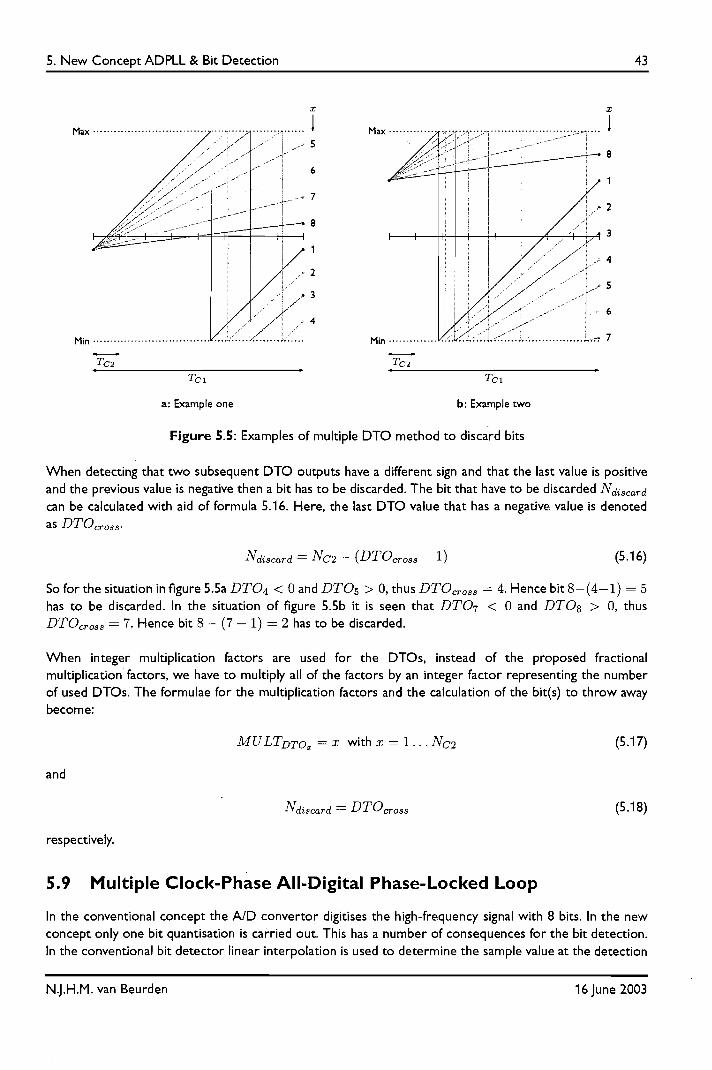
S. New Concept ADPLL & Bit Detection 43
x x
Max ........................................ : ............. , ....... 1 / .. , '/ 5
7
MUA+f~~ I 1/2
'4 3
,I /' '~:~/i/ 4
~l .' "// ·J./5 ~ • I
. / " ,/ • I 6
Min ............... c:.;{<L:·::<:.~ ................ L,! 7
6
_~-. 8
,../ ,
Min ...................................... ~,( .......... 1:. ... .
2
3
4
TC2
a: Example one b: Example two
Figure 5.5: Examples of multiple DTO method to discard bits
When detecting that two subsequent DTO outputs have a different sign and that the last value is positive and the previous value is negative then abit has to be discarded. The bit that have to be discarded Ndiscard can be calculated with aid of formula S.16. Here, the last DTO value that has a negative value is denoted
as DTOcross.
Ndiscard = NC2 - (DTOcross - 1) (S.16)
So for the situation in figure S.Sa DT04 < 0 and DTOs > 0, thus DTOcross = 4. Hence bit 8-(4-1) = 5 has to be discarded. In the situation of figure S.Sb it is seen that DT07 < 0 and DTOs > 0, thus DTOcross = 7. Hence bit 8 - (7 - 1) = 2 has to be discarded.
When integer mUltiplication factors are used for the DTOs, instead of the proposed fractional multiplication factors, we have to multiply all of the factors by an integer factor representing the number of used DTOs. The formulae for the multiplication factors and the calculation of the bit(s) to throwaway become:
MU LTDTOx = x with x = 1 ... NC2 (S.17)
and
N discard = DTO cross (S.18)
respectively.
5.9 Multiple Clock-Phase All-Digital Phase-Locked Loop
In the conventional concept the AID convertor digitises the high-frequency signal with 8 bits. In the new concept only one bit quantisation is carried out. This has a number of consequences for the bit detection. In the conventional bit detector linear interpolation is used to determine the sample value at the detection
N.J.H.M. van Beurden 16 June 2003
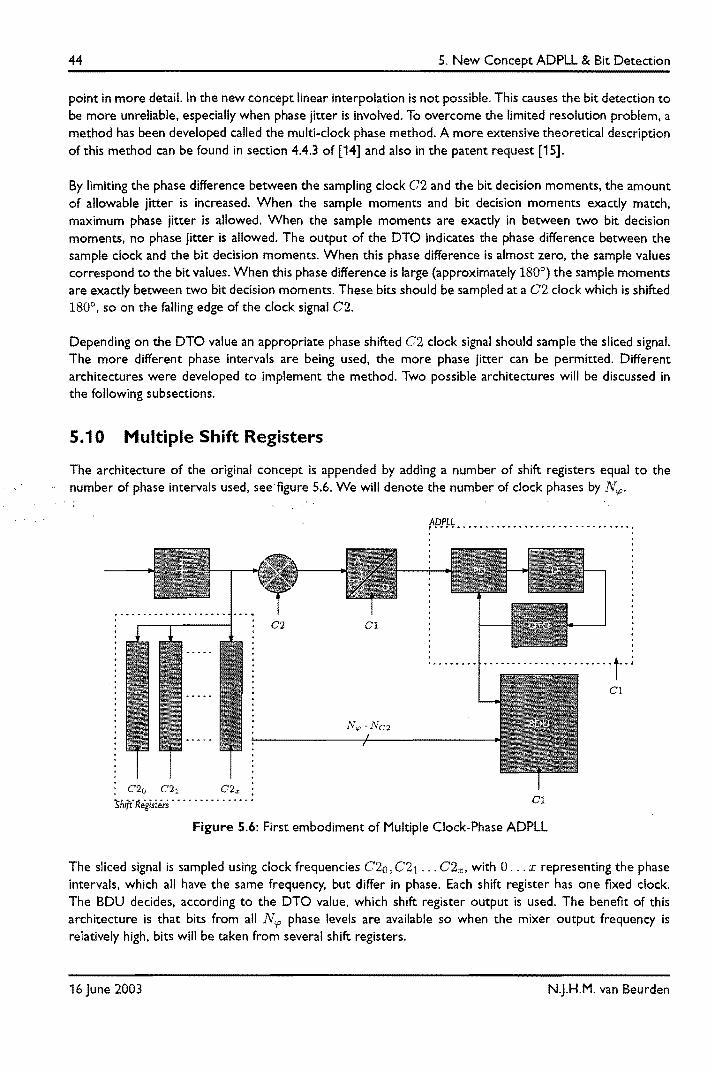
5. New Concept ADPLL & Bit Detection
point in more detail. In the new concept linear interpolation is not possible. This causes the bit detection to be more unreliable, especially when phase jitter is involved. To overcome the limited resolution problem, a method has been developed called the multi-dock phase method. A more extensive theoretical description of this method can be found in section 4.4.3 of [14] and also in the patent request [15].
By limiting the phase difference between the sampling dock C2 and the bit decision moments, the amount of allowable jitter is increased. When the sample moments and bit decision moments exactly match, maximum phase jitter is allowed. When the sample moments are exactly in between two bit decision moments, no phase jitter is allowed. The output of the DTO indicates the phase difference between the sample dock and the bit decision moments. When this phase difference is almost zero, the sample values correspond to the bit values. When this phase difference is large (approximately 180°) the sample moments are exactly between two bit decision moments. These bits should be sampled at a C2 dock which is shifted 180°, so on the falling edge of the clock signal C2.
Depending on the DTO value an appropriate phase shifted C2 clock signal should sample the sliced signal. The more different phase intervals are being used, the more phase jitter can be permitted. Different architectures were developed to implement the method. Two possible architectures will be discussed in the following subsections.
5.10 Multiple Shift Registers
The architecture of the original concept is appended by adding a number of shift registers equal to the number of phase intervals used, see figure 5.6. We will denote the number of clock phases by N'P'
I\Pfg ............................... . . .
....................... t··; C1
C20 C2l C2x • '!;h/ff ~eg;siers .........••.•.• C1
Figure 5.6: First embodiment of Multiple Clock-Phase ADPLL
The sliced signal is sampled using clock frequencies C20, C21 ... C2 x • with O ... x representing the phase intervals, which all have the same frequency, but differ in phase. Each shift register has one fixed clock. The BDU decides, according to the DTO value. which shift register output is used. The benefit of this architecture is that bits from all N<p phase levels are available so when the mixer output frequency is relatively high, bits will be taken from several shift registers.
16 june 2003 N.j.H.M. van Beurden

5. New Concept ADPLL & Bit Detection 45
5.11 Dual Shift Registers
The architecture of the original concept can also be appended by adding only two shift registers. see figure 5.7.
ADPU , ................. ., .............................................. . · . · . · . · . · . · .
·······················t··:
C1
C1
C21 C22 C2x •
"shill'itegisters ••••••.••••••••
Figure 5.7: Second embodiment of Multiple Clock-Phase ADPLL
The clock supplied to the shift register is now depending on the DTO output. Again the BDU decides, according to the DTO value which shift register output is used. A drawback of using only two register is that bits can only be taken from two succeeding phase levels. So, at a certain high mixer frequency bits are not available. In practice however. the output frequency of the mixer is relatively low so that two registers will suffice.
N.J.H.M. van Beurden 16 June 2003

6. New Concept Modelling & Simulation 47
Chapter 6:
New Concept Modelling & Simulation
The new concept was modelled and simulated to determine the behavior under various parameters and has been used as a reference for the implementation. In this chapter, the modelling and simulation of the new concept will be discussed. At the end some experimental results will be given.
6.1 Modelling
The modelling and simulation of the new concept was done in Mat Lab, like the conventional concept. The idea came up to improve the usage convenience by incorporating a Graphical User Interface (GUI). This GUI is developed with the GUIDE tool, which stands for GUI Development Environment, a tool present in Mat Lab 1. It is an object-oriented programming environment that offers a quick way of developing MatLab GUls. When compared to the conventional concept simulator, users do not have to change source code to configure the simulation settings. Moreover, new functions can be added orderly and the source code has a modular architecture.
When modelling the new concept, some source code could be reused from the conventional concept. The following subsections will describe the modelling of the different building blocks. The simulator architecture is as displayed in figure 6.1 .
...... ~ .. ~"~,, ..... ~ .... ., •• ~ ................. ~ ••• _ .... ___ ... _ .. __ ._ ..... __ .. __ ._ .... __ " ... "' __ .. _._ ... _ ..... ~ ....... ____ • __ ._._ •••••• • .. __ • __ ••••••• ... w ..................... ..
: Phase One
. t·. h .............. __ •••••• __ •• __ •• __ ... _ •• ••• •• • .. • ___ •• _._ •• _ ........... ____ • __ ............ _._ .. _ .......................... _ ......... _ ................... ..
Figure 6.1: Simulation flow
Because the input signal generation and preprocessing of the new concept takes a long time. the simulation flow was divided into two parts indicated by "Phase One" and "Phase Two" in figure 6.1. Especially the processing in the mixer takes a relatively long time because of the involved differential equations that were modelled in the simulator. The first part deals with the signals through the AID convertor. The second part deals with the processing of the ADPLL and Bit Decision Unit. By separating the processing, the input signals for the blocks of primary interest (ADPLL and BDU) can be loaded from a pre-generated file. This saves a lot of time.
1 Note that the GUIDE tool to create GUls only runs under the Windows version of MatLab currently in use, being MatLab 6 release 13. But the generated GUI can be run under both Windows and Unix operating systems though.
N.J.H.M. van Beurden 16 June 2003

48 6. New Concept Modelling & Simulation
The default filename extensions are displayed within the file symbols of figure 6.1. Some advanced user interface options are offered by the GUI. A screenshot of the simulator graphical user interface is displayed in figure 6.2.
Figure 6.2: Simulator graphical user interface
Each building block is displayed as a separate block and has its own software function2. There is a plotting window in the middle of the user interface. At its right top there are some buttons to scroll the x-axis and y-axis. On the right of the screen buttons and comboboxes are present. Starting from the top their functions are: savinglloading input for the ADPLL from/to a file, starting the simulation flow, plotting the output of a specified signal. selection of the signal to be plotted, postscript file creation, name specification for postscript output file, some advanced zooming and axis options, dosing the simulator and loading/saving the user interface settings. At the bottom of the GUI, there is a status bar giving information during the simulation about progress, errors and other information. The building blocks and their parameters will be discussed in more detail in the following subsections.
6.1.1 Signal Generation
The high-frequency signal to use for the simulations is generated using the same concepts described in section 3.1 of [14]. A file containing bits (representing the optical disc data) is read, up-sampled and MTF filtered to obtain a high-frequency signal. The default extension of the bit input file is . bi t as can be seen from figu re 6.1.
2 Actually, there are "functions" and "procedures" but in Mat Lab the general word "function" is always used.
16 June 2003 N.J.H.M. van Beurden

6. New Concept Modelling & Simulation 49
6.1.2 Slicer & Shift Register
The preprocessing consists of some analogue circuitry. To be able to simulate the continuous time behavior. the asynchronous discrete time values are stored together with their corresponding signal value.
After signal generation a slicer and shift register are present. To determine the zero-crossing levels more accurately in the simulator, interpolation is used. The number of interpolation points and the order of interpolation can be configured with the GUI. The time values and signal values (bit values) are stored in separate files with default extensions of . zct and . zca, respectively. This stored information will later be used in the BDU to recovery the channel bits.
6.1.3 Mixer
The mixer was simulated by means of an event-driven method. Only when one of the triggered signals changes an action is performed. The analogue part of the mixer uses linear first order differential equations to model the capacitances present in the OpAmp circuitry (see section 5.4). For calculations of the differential equations see Appendix B.
Before the mixer was actually realised in hardware, some simulations were carried out with the aid of Cadence Custom IC Design Tools, Pstar and Cgap. The Pstar and Cgap programs are created and supported within Philips Research. Pstar is an analysis program which performs analysis on discrete and integrated circuits. First, a schematic was drawn in Virtuos 0 Schemat ic Editor which is part of the Cadence Custom IC Design Tools. After finishing the drawing an input file for Pstar was generated. With this input file and some specified stimulus Pstar can be used to do simulations. The postprocessing of the simulations is done by Cgap which can create a visual representation of the simulated data.
6.1.4 AID Convertor
The output of the AID convertor is saved to a file which has a default file extension of . ana. In the GUI the offset and gain of the ND convertor can be set. Moreover, the AID conversion can be skipped.
6.1.5 New Concept ADPLL
Most of the internal structure of the conventional concept ADPLL remains the same for the new concept. The nominal frequency can be set by entering the increment to be added to the DTO ~ach 01 clock period. This increment can be calculated using equation 5.12. Also, the loop filter to be used can be specified. The initial DTO value can also be specified. Whilst the DTO consists of a 24 bits register containing a signed integer, a range between _223 ..• 223 1 can be specified. The phase detector can be set to only calculate the phase error when the ND convertor input Signal is between two specifiable levels (see section 6.2.2). The levels can be chosen within a range of _27 ... 27 - 1.
Finally some functions are offered to convert the sawtooth signal to a triangle signal. This functionality was never realised in practice, because no satisfying results were obtained in the simulator.
6.1.6 Bit Decision Unit
The choice can be made to use single or multiple DTO bit discarding method as discussed in sections 5.8.1 and 5.8.2. Also, the detected bits can be written to a file with a default file extension of . out.
N.J.H.M. van Beurden 16 June 2003

50 6. New Concept Modelling & Simulation
6.2 Implementation Problems & Solutions
During the implementation and simulation of the new concept some problems were faced. These will be discussed and possible solutions will be given in the next subsections.
6.2.1 Problems
When the DTO is not able to lock exactly to the output of the AID convertor, this has a number of consequences. In the phase detector, the DTO value and the sampled mixer output are subtracted from each other. When the maximum to minimum transitions of both signals do not exactly match a large phase error is generated while the phase difference should be approximately zero. The peaks in the phase error cause periodic disturbances in the system.
Also, at the maximum to minimum transitions of the mixer output signal, a bit has to be discarded. The mixer signal has disturbance and it is therefore better to use the transition of the DTO to discard bits. The mixer transition from maximum to minimum takes a few steps whilst the DTO signal switches from its maximum to minimum value in just one step. Because the DTO and AID phases do not match exactly, the wrong bit could be thrown away when the DTO is used as a reference instead of the mixer output. This problem was already solved by using the Multiple Clock-Phase method.
6.2.2 Possible Solutions
A way of improving the phase error and locking is by transforming the sawtooth signals to triangle signals. This way the transient will no longer be present. But converting. the sawtooth signal to a triangle signal gave a lot of problems.
It is also possible to only detect the phase when the signal lays in its linear part, so not close to its transition point, nor in its transition area. To be able to accomplish this, two levels can be defined. If the signal lays within these levels and is in the linear part the phase error is calculated. Else, the phase error is set to zero. Figure 6.3 illustrates this principle. Only within the grayed area the phase error is determined.
White = Set Phase Error To Zero _ ............................................................. +128
.. Upper Level
Gray = Calculate Phase Error -
.... . Lower Level White = Set Phase Error To Zero -
............................ -128
Figure 6.3: Thresholded phase detection principle
A quest was started for other methods. At first, it was accepted that bits will be discarded at the wrong moments but that a correction will take place according to the phase information available for each bit. Amongst other information, the down signal needed to be saved. An extra shift register was implemented which stores the information in files with extension . mtm and . mdw, for the time value of the down pulse and the signal value of the down pulse, respectively. This first method is not used in practice anymore because more optimal solution is provided by the Multiple Clock-Phase method which was described in section 5.9. This method is successfully implemented into the simulator.
16 June 2003 N.J.H.M. van Beurden

6. New Concept Modelling & Simulation 51
6.3 Experimental Results
Several measurements were carried out and were compared with the results in practice. Unless specified differently the following parameter values were used for the simulation results to come:
• Clock frequency: IC2 = 20 MHz • Bit rate: lbit = 19.98 MHz • The nominal frequency: I nom 20 kHz • Oversample factor: 20 • Clock divider factor: NC2 = 8 (so ICI 20/8 MHz) • MTF filter for Blu-ray Disc signal input • Mixer filter bandwidth: 72 kHz • DTO initially locked to input signal to prevent long simulations (DTO initially equals _223 - 1) • Thresholded phase detection boundaries of -80 .. . 80
6.3.1 Phase Step Response
In the simulator there is a possibility to obtain the step response, specifying the sample number at which to apply the step and the step size in degrees (0 . .. 359). Because the loop filter plays a very important role in the stability of the ADPLL its step response was observed. Applying a step in the simulator was done by translating step size to an increment for the DTO output at the specified time. Figure 6.4 shows the different phase error responses when a step was applied at sample 1000 with a phase increment of 180 degrees. The total amount of processed samples equaled 100000. It is clear to see that the thresholded phase error response of figure 6.4b has less disturbance than the non-thresholded phase error response of figure 6.4a. The behavior is as expected. the overshoot does not exceed 4% and the settling time equals about 32 msec for the current settings. as calculated in Appendix A. When a Blu-ray Disc signal is supplied to the simulator it is observed from figures 6.4c and 6.4d that the signal has periodic disturbance.
N.J.H.M. van Beurden 16 June 2003

52
~ f :;-~ ~ .. 1 f E .. l ~ Q
-<
¥ " ~ ! i 1 i 0
j i it Q 0(
lSO
100
50
-50
-100
-ISO 0 0.5 1.5 2.5 H <.5
T .... (_l lI::U(l
a: Phase error for non.thresholded phase detector, for runlength 4 signal
-50
-tOO
c: Phase error for non·thresholded phase detector, for Blu-ray Disc signal
... ! :;-! ~
J i 0
j J o! ~
6. New Concept Modelling & Simulation
Tlme {secondl} )( 10-1
b: Phase error for thresholded phase detector, for runlength 4 signal
1.5 3.5
d: Phase error for thresholded phase detector, for Blu· ray Disc signal
Figure 6.4: Phase error for phase step
6.3.2 Frequency Step Response
Optical disc systems should be able to track a frequency step (phase ramp) for a short period of time. Because the ADPLL has two integrators. one in the loop filter and one in the DTO. a frequency step should deliver a steady state error of zero. To observe this, a frequency step was applied to the ADPLL At which sample number to apply the step and the frequency step size can be specified. The step size has to be specified as an integer increment to be added to the nominal frequency register. Figure 6.5 shows the response when a frequency step was applied simulating 250000 samples. The frequency step was applied at sample number 1000 and the frequency increment was about 15% of the nominal frequency. It can be observed that the final error goes to zero after a frequency step.
16 june 2003 N.j.H.M. van Beurden

6. New Concept Modelling & Simulation 53
"iI
~ t-" c: ;e. ~
i :l::
! = 0
e -so .b
~ If ::I "-0 «
-ISO 0 0,006 0.008 0.01 0.012
Time (set:onds)
Figure 6.5: Frequency step applied to run length 4 sequence
6.3.3 Mixer
Some simulations were carried out on the mixer using a run length 4 sequence and a Blu-ray Disc input signal. Figure 6.6 shows some results for the mixer summator/integrator. Runlength sequences, as applied to
figure 6.6a reduce the disturbance in the output signal when compared to the varying runlength observed in figure 6.6b. This is also true for all the subsequent building blocks in the mixer like the output of the mixer filter seen in figure 6.7 or the output of the offset and gain OpAmp (figure 6.8).
N.J.H.M. van Beurden 16 June 2003

54
J I J
a: Mixer summator/integrator output with runlength 2 series (MatLab)
JOllftOm
6\11;101))
4i)I'.llm
lt~HJut
h,j
-lfjjdml
4{jlll.lnl
-MlflJilT!
.:m'!.Um jjJ} Ifltl fh! 15fhlu ,WIJ.Hu
'5,Hu 125 .. hl P:<Jiu
c: Mixer summatorlintegrator Cgap output with runlength 2 series
d: Mixer summator/integrator practical measurement with runlength 2 series
J I j
6. New Concept Modelling & Simulation
-.".~----------'-''------------:
It 10-4
b: Mixer summator/integrator output with Blu-ray Disc input signal (MatLab)
e: Mixer summatorlintegrator practical measurement with CD signal
Figure 6.6: Mixer summator/integrator outputs for different input signals
16 June 2003 N.J.H.M. van Beurden

6. New Concept Modelling & Simulation
a: Mixer filter output with runlength 2 series (MatLab)
c: Mixer filter Cgap output with runlength 2 series
d: Mixer filter practical measurement with run length 2 series
55
0.3
~ 0.2
0.1
I -0.1
J -<>.2
... .1
-o-.~
0
Time (second.) )( 10'""
b: Mixer filter output with Blu-ray Disc input signal (MatLab)·
e: Mixer filter practical measurement with CD signal
Figure 6.7: Mixer filter outputs for different input signals
N.J.H.M. van Beurden 16 June 2003

S6
1 t f
i I!J f
1.'
/1 1.'
2.1 /1 a
1.5
Ii 2'
2,3
2,2
2,'
a: Mixer output with runlength 2 series
c: Mixer output Cgap output with runlength 2 series
d: Mixer output practical measurement with runlength 2 series
l.6
2,5
i 2,4
1 I 2,)
l 2,2
2.1
6. New Concept Modelling & Simulation
Time (seconds)
b: Mixer output with Blu.ray Disc input signal
e: Mixer output practical measurement with CD signal
Figure 6.8: Mixer output plots
16 June 2003 N.J.H.M. van Beurden
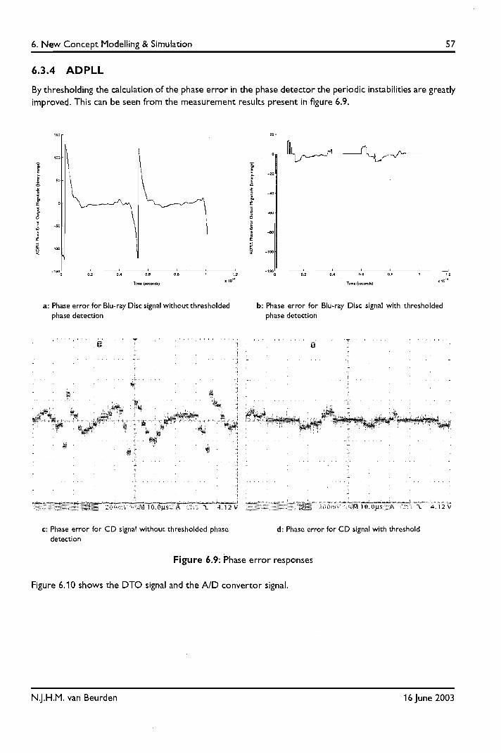
6. New Concept Modelling & Simulation 57
6.3.4 ADPLL
By thresholding the calculation of the phase error in the phase detector the periodic instabilities are greatly improved. This can be seen from the measurement results present in figure 6.9.
1SO
-so
-100
-150 0 0.2 0.6 0.' 1.2
Time (seco"ds) II 10·-
a: Phase error for Blu-ray Disc signal without thresholded phase detection
T
c: Phase error for CD signal without thresholded phase detection
r; ~ !; ;i
i I:
~
" l ~ ;f
~ Cl
"
20
-20
-60
-BO
-100
-1'20 0 0.' 0.' 0.6 0.' 1.2
Time (Iecondl) x 10~4
b: Phase error for Blu-ray Disc signal with thresholded phase detection
.",.
d: Phase error for CD signal with threshold
Figure 6.9: Phase error responses
Figure 6.10 shows the DTO signal and the AID convertor signal.
N.J.H.M. van Beurden 16 June 2003

58 6. New Concept Modelling & Simulation
150
100
-150{)~---'O-::C.2--70.':----:0.~. ----,o-::c .• ---:----:',..· ;II: 10~
Figure 6.10: Slopes of the DTO and AID convertor
6.3.5 Multiple Clock-Phase ADPLL
The Multiple Clock-Phase method was implemented into the simulator. It consists of 8 different phase levels, each covering 45 degrees of the DTO. To be able to verify the feasibility of this method, apprOXimately 300000 channel bits coming from a Blu-ray Disc are supplied to the simulator and processed using this method. By comparing the original bit file with the file containing the regenerated channel bits, the correct functioning was proven. No extensive simulations could be done though, due to the lack of time.
6.4 ADPLL Key Parameters
The key parameters of the ADPLL, being the hold range, lock range, pull-in range and pull-out range, are dependent of a great number of parameters. For this reason, determination of the key parameters using formulae or the simulator is difficult. Different settings will result in different outcomes. Moreover, no clear definition of the key parameters can be found in literature. The results given in this section must therefore be considered being preliminary.
The number of bits used for the phase detector output will be denoted as Npd and represents a signed integer number. The output range 0 Rpd of the phase detector equals:
(6.1)
The output range of the proportional part of the loop filter ORlf,P is dependent on the proportional gain Kp and the maximum output range of the phase detector ORpd:
(6.2)
The frequency range that can be adjusted with the integrating part of the filter depends on the number of bits used for the integrator register NJ and the integrating gain K J. For the output range of the integrating part of the loop filter ORlf,J the following formula is obtained:
(6.3)
The used phase detector for both cOricepts cannot handle phase error values that exceed the range of -180° ... 180°.
16 June 2003 N.J.H.M. van Beurden

6. New Concept Modelling & Simulation 59
6.4.1 Hold Range
The hold range LMH is the frequency range for which a PLL can lock but not necessarily will. It could maintain phase tracking within this range. The hold range is equal to the maximum frequency amount the
loop filter can regulate, so to the maximum output of the integrating branch of the loop filter. Therefore,
this range is limited due to the limited word length of the implemented integrator register. No lock will be obtained when the integrator register exceeds its maximum value.
The maximum amount of increment the integrating part of the loop filter can give equals 0 R1f,!, so to the nominal frequency a maximum of ORI!,! can be added. The hold range in percent to the nominal frequency
thus equals:
6.4.2 Lock Range
ORI!I 6WPI = 100· --'
Nnom (6.4)
The lock range 6WL is the reference frequency range for which the ADPLL can regulate to the reference frequency when it is out of lock. When regulating fDTO to fbit. the phase error may not exceed the maximum phase detector output.
6.4.3 Pull-In Range
To determine the pull-in range 6WPI, the PLL starts with a frequency difference. Then, the integrator is reset. The frequency range for which the PLL can lock using this procedure is the pull-in range. The PLL will always lock, but not necessarily without exceeding a phase error of 1800
• This process can take a long
time.
6.4.4 Pull-Out Range
When the ADPLL is locked and a reference signal is supplied which contains a step frequency larger than the pull-out range 6wpo the ADPLL cannot maintain lock. Following the literature [2] it cannot be calculated
though the pull-out range lays somewhere between the lock range and pull-in range:
(6.5)
6.S linear Phase
A linear phase characteristic is of great importance for data transmission systems. It implies that every signal frequency undergoes the same amount of time delay. The delay at one particular frequency is called the phase delay. The delay characteristics of a certain frequency range (a group of frequencies) is called
the group delay. A linear phase relationship results in a constant group delay when differentiating. An equal delay for all frequency components maintains the waveform properties, like the zero-crossing moments of
the signal. The analogue low-pass filter within the mixer is an example of a circuit requiring a linear phase relationship to reduce lSI. This filter can be seen as an anti-aliasing filter and is located before the AID convertor.
A solution is to straightforward linearise the phase by a different OpAmp configuration. With the so-called Bessel-Thomson method, low-pass filters can be created with approximately constant time delay. Here, the coefficients in the polynomials of the filter transfer function are closely related to Bessel polynomials.
For a proper solution a higher order filter is required. Every time the order is raised by two the number of OpAmps required increases by one. Examples of Bessel-Thomson filters, implemented by using OpAmp
N.J.H.M. van Beurden 16 June 2003

60 6. New Concept Modelling & Simulation
circuits can be found in [17]. chapter 10.
The magnitude of the Bessel-Thomson filter is neither constant over a wide range of frequencies through the pass band. nor does it have a very sharp cut-off in the transition region. Thus. the roll-off is more gradual. If substantially stop band attenuation is required. a Bessel-Thomson configuration of a high order is required. This requires a very complex OpAmp circuit. It might therefore be better to use a so-called delay equaliser instead. Delay equalisers are all-pass filters and are suited to reconstitute a signal with little or no distortion just like Bessel-Thomson filters. The delay equaliser should be placed in series. behind the filter. The resulting delay of the original filter followed by the delay equaliser is constant over the specified frequency band and the amplitude response of the filter remains approximate~y the same.
For more information on linear phase circuits. see Appendix C.
16 June 2003 N.J.H.M. van Beurden
7. Conclusions 61
Chapter 7:
Conclusions
In this final chapter results and recommendations for future research issues will be discussed.
7.1 Results
The conventional and new concept ADPlL and bit detector have been investigated. An experimental environment (prototype) was created to implement and test both concepts in practice. Communication between a cabinet and a computer was realised. Control software can send firmware to the programmable logic present on the cards within the cabinet and various firmware parameters can be controlled. An extension card has been developed to be able to send/receive information to/from the prototype.
The old concept was successfully designed and implemented in firmware. Practical measurements (e.g. step response) matched the simulation results carried out in MatLab:
• The ADPLL was dependent on the sample frequency. This was solved by using an extra gain factor which is proportional to the nominal frequency.
The new concept was successfully modelled and simulated under Mat Lab, a graphical user interface improves the ease of use of the simulator. Simulation results were compared to the response of the implemented hardware and matched. The feasibility of the new concept was proven. Conclusions:
• The concept described in the patent [7] cannot be implemented straightforward in practice when phase jitter is present. Because of phase jitter. wrong bits can be discarded. The actual phase information per bit is needed to regenerate the channel bits. the average phase information is not enough. This problem was solved by using the so-called Multiple Clock-Phase method. although practical limits still exist. The method was filed for a possible patent and was implemented into the simulator. Preliminary results prove that the method works correctly.
• The division factor of the dock is limited because it has a relation with the bandwidth of the ADPLL. • To perceive a satisfying sawtooth signal the mixer output frequency has to be low. A difference
of maximally 1 % may be present between the channel bit frequency fbit and the sample clock frequency fC2.
7.2 Recommendations
Some future investigation could include: • An investigation could be started to search for other implementations of the mixer to prevent
periodiC disturbances and to be able to obtain higher mixer output frequencies. • Implementation of a frequency loop for the conventional concept. This frequency loop is needed to
do further measurements with an optical player. Also, the frequency loop for the new concept can be modelled, simulated, implemented and practically tested.
• Implementation of a phase linear circuits for all low-pass filters. It is also recommended to do further investigation on the possibilities delay equalisers offer compared to Bessel-Thomson methods.
• Measurements with an optical player. For example, Bit Error Rate (BER) calculations could be carried out to indicate the quality of both concepts.
• Optimisation of the MatLab source code for less time consumption and better memory usage.
N.J.H.M. van Beurden 16 June 2003

Bibliography 63
Bibliography
[1] Bellescise, H. de, "La Reception Synchrone", Onde Electrique, vo1.11, 1932. [2] Best, R.E., "Phase-Locked Loops: Design, Simulation And Applications", Fourth Edition, London: McGraw
Hill, 1999, ISBN: 0-07-134903-0. [3] Blum, M.W. & Immink, AH.J. & Verberne, H.R.M., "Software Framework (In Visual C++)", Eindhoven:
Philips Research Laboratories, Report Number: 2003-2376, Preliminary Version.
[4] Bouwhuis G. & Braat J. & Huijser A & Pasman J. & Rosmalen G. van & Schouhamer Immink, K., "Principles Of Optical Disc Systems", Englewood Cliffs: Prentice-Hall, 1991.
[5] Gardner, EM., "Phase Locked Techniques", Second Edition, New York: Wiley, 1980, ISBN: 0-471-04294-3.
[6] Gill, G.S. & Gupta, S.c. "First-Order Discrete Phase-Locked Loop With Applications To Demodulation Of Angle-Modulated Carrier" IEEE Transactions On Communications, University Alabama, Huntsville, AL, USA vol. COM-20 Oune 1972), no. 3, pages: 454-462.
[7] Kahlman, J.AH.M~, "Bit-Detection Arrangement And Apparatus For Reproducing Information", Eindhoven: Philips Research Laboratories, patent. Request Date: 21 November 2001.
[8] Nise, N.S., "Control Systems Engineering", Second Edition, Addison-Wesley, 1995, ISBN: 0-8053-5424-7.
[9] Otte, R., "A New Generic PCB For Use In A Standard Cabinet - Generic 1/-", Eindhoven: Philips Research Laboratories, 8 December 1999, Version 1.5.
[10] Otte, R., "A Sample Rate Convertor For Synchronous Bit Detection", Eindhoven: Philips Research Laboratories, 2 November 1999, Version 1.0.
[11] Persoon, G.G. Collegediktaat Voor Het Vak Niet-Lineaire Elektronica VKO (SF140) Eindhoven University of Technology, Faculty of Electrical Engineering, Edition: September 2000, pages: 85-105.
[12] Plassche, R. van de, "Integrated Analog-To-Digital And Digital-To-Analog Convertors", Dordrecht: Kluwer Academic Publishers, 1994, ISBN: 0-7923-9436-4.
[13] Pohlman, K.C., "The Compact Disc Handbook", Second Edition, Oxford: Oxford University Press, 1992, ISBN: 0-19-816327-4.
[14] Rutten, AJ.A., "A New High-Speed All-Digital Phase-Locked Loop For Optical Recording", Eindhoven: Philips Research Laboratories, 2003.
[15] Rutten, AJ.A, Beurden, N.J.H.M. van, Kahlman, J.A.H.M., Immink, AH.J. "Improved Jitter Insensibility Using Multiple Clock-Phase Bit Detector In High-Speed All-Digital Phase-Locked Loop", Eindhoven: Philips Research Laboratories, patent.
[16] Sallen, R.P. & Key, E.L. "A Practical Method For Designing RC Active Filters" IRE Transactions On Circuit Theory, 1955, vol. CT-2, pages: 74-85.
[17] Schaumann, R. & Valkenburg, M.E. van, "Design Of Analog Filters", Oxford: Oxford University Press, 2001, ISBN: 0-19-511877-4.
[18] Stan, S., "The CD-ROM Drive: A Brief System Description", Dordrecht: Kluwer Academic Publishers, 1998, ISBN: 0-7923-8167-X.
[19] Stan, S., "Optimization Of The CD-ROM System Towards Higher Data Throughputs", Eindhoven: Eindhoven University of Technology, 1999, Doctoral Dissertation.
[20] Stikvoort, E.E & Rens, J.A.c. van, "Digital Bit Detection In The Compact Disc", Eindhoven: Philips Research Laboratories, 1990, NatLab Report Nr. 6350.
[21] Stikvoort, E.E & Rens, J.A.c. van, "An All-Digital Bit Detector For Compact Disc Players", IEEE Journal On Selected Areas In Communication, vol.10 Oanuary 1992), no. 1, pages: 192-200.
N.J.H.M. van Beurden 16 June 2003

64 Bibliography
[22] Stikvoort. E.F. & Rens, JAC. van & E.C. Dijkmans. "Phase-Locked Loop Orcuit And Bit-Detection Arrangement Comprising Such A Phase-Locked-Loop Circuit", Eindhoven: Philips Research Laboratories. patent.
[23] Westlake. P.R .• "Digital Phase Control Techniques". Electronics Institute of Radio Engineers Transactions On Communications Systems. vol. CS-8 (December 1960). pages: 237-246.
16 June 2003 N.J.H.M. van Beurden

Appendix A: New Concept ADPLL System Calculations
Appendix A:
New Concept ADPLL System Calculations
65
The architecture for the ADPLL in the z-domain is given in figure A.1. The z-domain was chosen because digital systems can easily be modelled in this domain .
• . • f'P. ••. , ••.•...•.•.... . if. . . . . . . . . . . . . . .• . .......... P.TP.. •••••••••••• . " ' i I, •
---'---tot
* ........ ... ,z.
Figure A.1: Model in z-domain of implemented ADPLL
To be able to track a phase step and a frequency step two integrators are needed. One integrator lets the steady state error be zero after a phase step, two integrators let the steady state error be zero after a frequency step. Because just two integrators do not make a stable system, a zero is added. The loop filter therefore contains one pole in the origin and a zero at a position We>' The open loop transfer function of the loop filter is displayed in figure A.2.
logIH(jw)' (dB) )
-log w (rad/sec)
Figure A.2: Open loop transfer function of loop filter
The second order, open loop transfer function of the total ADPLL is displayed in figure A.3. We have one pole in the origin due to the integrating branch of the loop filter and another pole in the origin because of the DTO. This causes the -40 dB/dec segment. A zero is present at the point We>. reducing the slope by -20 dB/dec from that point on. The cut-off frequency is located at Wo and Wn is the natural frequency (frequency if no damping were present).
N.J.H.M. van Beurden 16 June 2003

66 Appendix A: New Concept ADPLL System Calculations
logllI(jw)1 (dB) 1 .40 dB/dec
•
.. . .. 2( 2(
4(2
-log w (rad/sec)
Figure A.3: Open loop transfer function of total PLL
The dosed loop PLL transfer function delivers a low-pass filter that falls of with -20 dB/dec at radial frequency woo We also know that (see [S], page 23):
(A.1)
In the following text the proportional gain of the loop filter will be denoted by K p and the integrating gain by Kl: . .
A.1 Overshoot
The transfer function for the DTO equals:
1 KDTO~
The transfer function for the loop filter equals:
The complete dosed loop transfer function of the ADPLL in figure A1 equals:
(KpZ-l + KJ-i:r )KDTo-i:r
1 + (Kpz-l + KJ z~l )KDTO Z~l
(A2)
(A3)
(AA)
We want to determine the behavior in the frequency domain. Therefore, substitute z 0-0 ejwTs with the sample period and w the radial frequency, to transfer from the z-domain to the s-domain:
z (AS)
We may approximate equation AS (with is and i = ~) when is » i, giving:
(A6)
16 June 2003 N.J.H.M. van Beurden

Appendix A: New Concept ADPLL System Calculations 67
The same result is obtained for 1
1 (A7)
The final transformation thus becomes:
KpKDTO(l z-l) + KIKDTO KpKDTO(jwTs) + KIKDTO
(z - 1)2 + KpKDTO(l Z-l) + KIKDTO 0-0 (jwTs)2 + KpKDTO(jwTs) + KIKDTO (AS)
The standard system response for a linear second order system with two poles and one zero equals:
Here the poles are located at:
And the zero is at:
This results in (with s jW):
2(wn s + wn2
s2 + 2(wn s + wn2
PI
P2
2(wn s+ wn2
s2 + 2(wn s + wn2
So the natural radial frequency Wn and the damping ratio ( equal:
( =
(A9)
(A10)
(A11)
(A12)
S2 + ';'KpKDTOS+ #;KIKDTO (A 13)
(A14)
(A1S)
This results in the following gain factors for the proportional (Kp) and integrating (KI) parts:
(A16)
Kp = (A17)
To determine how the overshoot relates to the damping ratio for the transfer function of A9 a step is applied:
1 (A1S)
S
Or in partial fractions:
1 s (A19)
S
N.J.H.M. van Beurden 16 June 2003

68 Appendix A: New Concept ADPLL System Calculations
Rewriting:
1 8
8 (8 + (wn )2 + wau - (2)
Now translate to the time-domain with aid of the following Laplace transformation pairs 1:
8 ~ sin(bt)]
s
Transforming:
--;===~ sin(wn vit=(2t)]
To find the highest output. differentiate and find the roots:
Thus:
The following answers are then found:
arctan (2'2~) -7r
wn vit=(2
(2"1i=z2) arctan 2(T=r + 7r
WnV1 - (2
(2"1i=z2) arctan 2~
wn vit=(2
o
(A20)
(A21)
(AU)
(A23)
(A24)
(A25)
(A26)
(A27)
(A28)
These points correspond to the highest and lowest outputs of the step response. By substituting these points into the step response equation the relationship for the amount of overshoot is obtained. Substitution gives:
arctan 2(~) -, 2(-1 ~
t} ===? 1-e 1-(2 + (1-() sign(2(2 - 1) (A29)
a.rctan
-( t2 ===? 1 e sign(2(2 1) (A30)
arct.,an
t3 1+e -(
sign(2(2 1) (A31)
Laplace transformation pair of equation A.21 can be found on W"W"w. vibrationdata. com/Laplace .htm
16 June 2003 N.J.H.M. van Beurden

Appendix A: New Concept ADPLL System Calculations 69
We only use t2 and tg to determine the overshoot ratio, tl gives a trivial result. The results for t2 and tg can be combined to:
a.tctan ~,.;.=:'-
2 -(----".,..,.;=;;:---"--(1-step(2(2-1))~. (2 ) 1 + sign(2( - l)e Vl-(2 slgn 2( - 1
Which reduces to:
The overshoot function in percents then equals:
%OS 100· e
The graph is displayed in figure A4:
100~--.r---.---~-----r----r----.----.------
80
60 Cf:J a ~
40
20
0 0 0.5 1.5 2
(
2.5 3 3.5
Figure A.4: Overshoot in percents depending on damping factor (
Solving the previous equation when 4% overshoot is wanted:
(4% >:::: 2.2239
4
(A 32)
(A33)
(A34)
(A35)
Because ( > 1 the system is overdamped. Now the K p and K J factors can be calculated, as an example it is assumed that the natural frequency equals 1000 Hz, thus a natural radial frequency of Wn = 27T" 1 000 and that the filter runs on a clock frequency of 20 MHz divided by a factor of 8, thus Ts = 2o.io6 . 8 = Also, KDTO equals 2-16:
KJ (wnTs? KDTO
20007T' 1 ) 2 1 2 . 2.22392.5 . 106 >:::: 0.0209 (A36)
Kp 2(VKi
y'KDTO 2· 2.2239y'0.0209 . /2!16 >:::: 164.7099 (A37)
N.J.H.M. van Beurden 16 June 2003

70 Appendix A: New Concept ADPLL System Calculations
A.2 Settling Time
We found the following equation after transformation (see equation A.23):
First, rewriting this equation by using the following formula2:
Giving:
.Resulting in:
2aeAt cos(Bt) 2beAt sin(Bt) = 2J a2 + b2 • eAt. cos (Bt arctan (~) )
a
b
A
B
1
Wn~
1 - l' + ( h ) 'e - (wo ' cos ( J w; (1 - (2)t - ,",ctan --;:::===
1-
1-
cos (wn ~t - ,",ctan --;;===
cos (wn ~t - ,",cian -----;==:=;;;:
(A.38)
(A.39)
(A.40)
(A.41)
(A.42)
(A.43)
(A.44)
In order to find the settling time, the time must be found for which this equation stays within x% of the steady state value. At the settling time the following relationship could be used:
COS (wn ~t - arctan h) = 1 1 - (2
(A.45)
When assuming this, a simple equation can be derived for the settling time. But it turned out that this conservative estimate may not be used in our case, for it is only valid when ( S; 1. When not assuming that equation A.45 holds, equation A.44 is hard to solve. Therefore, the settling time is determined directly from the step response plot shown in figure A.5. From this figure it also becomes clear that the peak output when applying a step to the system does not exceed 4%, as calculated.
2This Laplace transformation can be found in Appendix B of [2], page 365, equation B.2ge
16 June 2003 N.J.H.M. van Beurden

Appendix A: New Concept ADPLL System Calculations 71
I I I I I I
":':::::::':: .. :::::::::::::::::::::::::::::::::::::: .. : ..................................... :.:: ...... .
0.8 - -Gi
-0 0.6 ,- -.E Ci. E «
0.4 -
0.2 -
0 I I I I I I I I I
0 0.0005 0.001 0.0015 0.002 0.0025 0.003 0.0035 0.004 0.0045 0.005
Time (sec)
Figure A.S: Settling time determination via step response within 2% of final value (dotted lines)
It can be seen that the settling time within 2% of the final value equals (for the found (4% value):
Ts ,2% ;:::: 3.25 ms (A.46)
N.J.H.M. van Beurden 16 June 2003

Appendix B: New Concept Mixer Transfer Functions & Differential Equations
Appendix B:
New Concept Mixer Transfer Functions & Differential Equations
For the schematics of the various mixer OpAmp circuits to be calculated, see figure 5.3.
B.1 Summator/lntegrator
73
The resistor in the feedback loop of the OpAmp and in resistor present at the negative input of the OpAmp are chosen to have the same value. This value will be denoted as R. Following Kirchhoff's law:
CVout = 1
= RC Vin 1
RC 1
RC t
1 Vin J dr
r=O 1 'T t
RC Vin[RCeRC]o + c
1 t
RC Vin(RCe 1fC - 1) + c
-1) + c -t ) + ceRC
The initial voltage over the capacitance equals Vout(O) Vc. This results in
Thus:
-t
) + Vce RC
Here Vc is the previous output voltage and the interval is T, so:
(B.1)
(B.2)
(B.3)
(BA)
(B.S)
(B.6)
(B.7)
(B.8)
(B.9)
(B.10)
(B.11)
(B.12)
(B.13)
The found differential equation is not used in the simulator, for reasons discussed in chapter 5.
N.J.H.M. van Beurden 16 June 2003

74 Appendix B: New Concept Mixer Transfer Functions & Differential Equations
B.2 Filter
The resistor in the feedback loop of the OpAmp is denoted by R2 and the OpAmp present at the negative input of the OpAmp is denoted by R I . The response in the s-domain equals:
Vout =
\lin Vout R2'
\lin (R2 + Vout R2
\lin sRI R2C + Rl
In our case Rl = R2 = R so further reduction gives:
1
sRC+l
(B.14)
(B.15)
(B.16)
(B.17)
(B.18)
So the -3 dB point lays at W-3dB = R:C For the differential equation the same result as presented in equation B.13. It was used into the simulator.
B.3 Gain & Offset
Because the gain & offset circuit does not contain any capacitances it has no differential equations, therefore only the transfer function is derived. Resistors ROl and R02 are used to control the offset of the OpAmp using the offset circuit present at the positive input of the OpAmp. The resulting resistor value from the fixed resistance with the adjusted value of the potentiometer equals ROl. The remainder of the potentiometer resistance together with the resistance of the right resistor equals R02. Moreover, the gain is determined by the resistor in the feedback loop of the OpAmp, which will be called RG2 and the resistance present at the negative input of the OpAmp denoted as RGI.
\lin - V_ with V_ V+ (B.19)
RGI Vout V_ - IinRG2 (B.20)
Vout V+-\lin - V_
(B.21)
Vout V++ If; RG2
mRGl (B.22)
Vout = V+(1 + RG2 If; RG2 m RGI
(B.23)
V+ 15 R02 ROl + R02
15 ROl ROl + R02
(B.24)
Vout (15 R02 ROI + R02
lr: ROl ) (1 RG2 ;) ROl + R02 + RGl
_ If; RG2 mRGI
(B.25)
16 June 2003 N.J.H.M. van Beurden

Appendix C: New Concept Mixer Calculations 75
Appendix c: New Concept Mixer Calculations
The initial circuit of the mixer filter is displayed in figure C.1.
C =2.2nF
Figure C.1: Mixer filter implementation
The transfer function is given by:
H(jw) = _ R2 . __ I-=--::: Rl 1 +
(C.1)
The -3 dB point is located at a radial frequency We = R;C' The phase relationship <p (argument) equals:
<p(W) = - arctan(wR2C) (C.2)
Figure C.2 shows the phase bode plot of the transfer function.
180
175
170
165 -;;;-w 160 w .... ~
155 :E. w VI 150 til .s: a..
145
140
135
130 50 100 150 200 250 300 350 400 450 500
Radial Frequency (krad/sec)
Figure C.2: Mixer filter phase relationship
From section 4.2 of [14] it was experimentally determined that at least 30 pulses are needed to get
N.J.H.M. van Beurden 16 June 2003

76 Appendix C: New Concept Mixer Calculations
a acceptable mixer output signal. This means that the frequency difference between the clock and bit signals (fmixer) cannot exceed 1 %. The bit frequency for CD equals 4.32 MHz. Therefore, a maximum bandwidth of 1 % . 4.32 . 106 43 kHz is required. However; whilst the output signal of the mixer is a sawtooth signal some higher frequencies have to be included to get a acceptable waveform. Practical experiments have shown that the bandwidth of the filter has to have a factor 1.5 to 2 more bandwidth. So a required bandwidth of around 70 kHz is needed. Readily available values were chosen for the resistors and capacitance: Rl R2 = 1 kn and C = 2.2 nF. So the cut-off frequency equals We ~ 455 krad/sec or fe ~ 72 kHz.
A sawtooth waveform can be described by the following Fourier series:
x 1 f(t) = L -- sin(21Tnt)
n1T n=l
(C.3)
Here x determines the number of harmonics involved. Parameter x has to be a positive integer number. The more harmonics, the better the waveform looks like an ideal sawtooth. Figure C.3 gives some plots for a different number of harmonics. When only the first harmonic is parsed, a sine wave is obtained, which is not desired (see figure C.3a). If x is chosen to be greater than one sawtooth waveform is obtained of incremental quality. The sawtooth for two harmonics is given in figure C.3b and for ten harmonics in figure C.3c.
Time (sec)
a: 1 harmonics
Time (sec)
b: 2 harmonics
Time (sec)
c: 10 harmonics
Figure C.3: Fourier approximation of a sawtooth signal with a various number of harmonics
The group delay 7 g equals:
(CA)
The group delay plot is shown in figure CA.
16 June 2003 N.J.H.M. van Beurden

Appendix C: New Concept Mixer Calculations 77
2.5e-06 ,---..,-----,.--.,----.----,---r---,...----,,.....--.,-----,
2e-06
U' Q)
~ 1.5e-06 i;-ijj Q ~ ::l 1e-06 e
I!)
5e-07
OL--~-~--~-~-~--~-~-~~-~-~
o 50 100 150 200 250 300 350 400 450 500
Radial Frequency (krad/sec)
Figure C.4: Group delay 7g of the original mixer low-pass filter
Analogously, the group delay can be expressed in number of bit periods (or simply bits) the signal is shifted. The following formula may be used:
7g (bits) (C.S)
The group delay is not constant for the pass band frequency range. It can be observed from figure CA that the group delay differs by 1.25 f.tS over the de'sired frequency range, which is equal to a relative shift of SA channel bit periods. This causes unwanted dispersion which can be corrected by design methods perceiving linear phase. Two methods will be discussed in the following sections, being the Bessel-Thomson polynomial approximation and delay equalisation.
C.1 Bessel-Thomson
The poles of Bessel-Thomson polynomials cannot be simply determined by some rule but can be routinely found by computer methods. Tabulated coefficients and design curves were used. We choose a BesselThomson polynomial of the fourth order. This allows us to have about 4% deviation in the phase over the selected range which should be sufficient to stabilise the group delay significantly. The normalised transfer function, with Snorm = jWnorm the normalised radial frequency term, is equal to:
9.14013 11.4878 (C.6)
S~orm + 5.79242snorm + 9.14013 . s~orm + 4.20758snorm + 11.4878
The OpAmp circuit representing the Bessel-Thomson transfer function can be realised via a so-called Sallen-Key [16] circuit. Sallen-Key is used because it provides a very small pass band deviation, the active low-pass filter circuit is shown in figure C.S. Conductances and resistors are indicated. Calculations will be done follOWing [17], for this reason it is chosen not to replace the conductances in the circuit of figure C.S by resistors.
N.J.H.M. van Beurden 16 june 2003

7S Appendix C: New Concept Mixer Calculations
Figure C.S: Sallen-Key active low-pass filter circuit
The gain of the filter equals:
(C.7)
When the gain is set to be K = 1 the following transfer function in obtained:
(C.S)
To calculate the resistor and capacitance values. the transfer function of equation C.S is compared with the standard second order transfer function with two poles:
2 WnonT>
82 + Wnonn 8 + w2 Q norm
(C.9)
Where Q is the quality factor Q We desire the cut-off frequency to be about 75 kHz (470 krad/sec), according to earlier calculations. Figure C.6 shows the resulting bode diagrams. Subfigure C.6a shows the magnitude of the filter in dB and subfigure C.6b shows the phase relationship on a linear radial frequency scale. A linear scale was chosen to be able to observe the phase linearity in more detail.
16 June 2003 N.j.H.M. van Beurden

Appendix C: New Concept Mixer Calculations 79
a: Magnitude plot (dB) b: Phase plot (linear)
Figure C.6: Bode diagrams of determined filter transfer function
If the sampling interval is not small enough compared with the signal time course the signal will be distorted, this process is termed aliasing. The sampling rate necessary to avoid aliasing is given by the Nyquist theorem:
fnyq 2· fmax (C.10)
So the Nyquist theorem states that a sample rate of two times the maximal frequency of the signal is needed to avoid aliasing errors. In actual practice, 2.5 times should be the minimum to provide some margin for error. Many signals already have a limited spectrum, but for broad spectrum signals an analogue low-pass filter must be placed before the data acquisition system. The highest possible frequency the AID convertor has to sample depends on the shortest runlength which will be denoted as Rmin and the channel bit frequency fbit. The highest frequency is determined by the minimal run length containing only ones followed by a minimal runlength sequence of only zeros, vice versa. Thus the highest frequency is determined by:
f· - fbit max - 2. R
min (C.11)
Thus the Nyquist frequency becomes:
fnyq = 2 . fmax = (C.12)
For CD Rmin equals 2 and fbit equals 4.32 MHz. The clock frequency C2 is down-sampled by a factor NC2
and denoted by the frequency fCI. Thus the minimum sample frequency of the AID convertor yields:
fbit fsample,AID,min = No R
C2' min (C.13)
It can be observed from figure C.6 that the phase remains approximately linear until the specified range. The AID convertor can sample frequencies up to 1.7 Mradlsec for a CD system with NC2 = 8, before sampling problems with aliasing start to occur. At the calculated frequency the attenuation should be
N.j.H.M. van Beurden 16 June 2003

ao Appendix C: New Concept Mixer Calculations
sufficiently large so that no problems should occur with respect to aliasing.
The group delay as a function of w for the calculated filter is approximately:
1.175.108 (4.3479.1096 • w6 + 1.2966.10109 . w4 + 3.3413.10121 . w2 + 5.1665.10133)
1.0870.1098 . w8 + 2.4013.10110 . w6 + 7.1605.10122 . w4 + 1.8451 .10135 . w2 + 2.8531 .10147
(C.14) The resulting group delay graph is displayed in figure C.7.
2.12775e-06 ,...--.,..--"T'""-..,---,--....,..----r---r---,--r----,
2.12770e-06
'U' 2.12765e-06 <11 ~
i:! (ii 2.12760e-06 0 Q. ::l e
2.12755e-06 I.J
2.12750e..o6
2.12745e-06 L..-_.l...-_...I.-_-'--_....L..._......L.._--L_--L_---I._---ll...-.---I
o SO 100 150 200 250 300 350 400 450 500
Radial Frequency (kradlsec)
Figure C.7: Group delay for the Bessel-Thomson polynomial low-pass filter
As can be seen the relative group delay has been decreased a lot. Until approximately 300 rad/sec the group delay stays very constant. After 300 rad/sec the delay increases somewhat more. From 300 ... 500 krad/sec the group delay difference is about 26 ns. This corresponds to a relative channel bit shift of 0.11 which is much better than the results without linearising the phase.
The fourth order Bessel-Thomson method filter can be implemented by cascading two Sallen-Key OpAmp configurations. The resulting architecture is shown in figure c.a. Here the gain is set to K 1 so that resistors Ra 00 and Rb = 0 within figure c.S so that they are redundant and not included in the circuit of figure c.a. The second digit of the elements subscript indicates the first or second module of the cascade. If no second digit is present the equation holds for both modules.
Figure C.S: Fourth order Bessel-Thomson filter with Sallen-Key architecture
16 June 2003 N.J.H.M. van Beurden

Appendix C: New Concept Mixer Calculations 81
When solving equation C.8 with aid of equation C9 for both cascaded second order transfer functions. the following requirement for C1 and C2 of both filters results:
C 21 < 0.9175 (CiS)
C ll
C22 < 0.3820 (C.16)
C 12
G 1 + G 2 WnormCl
(C17) Q
G2 = W;orm C I C 2 (C.18)
G 1
The restrictions to the capacitances (equations CiS and C.16) are due to the fact that else solution are found having imaginary parts. By constraining the capacitance ratio we no imaginary valued answers are found. which are needed for practical implementation. From C.17 and C.18 it follows that:
Gu = 1.6040 . W norm . Cll
G 12 = 1.0446· Wnorm . C 12
Selecting readily available capacitor values results in:
C ll 2 nF
C21 = 1 nF
C 12 5 nF
Cn ~ 1 nF
Now calculating G1 for both modules:
. (C19)
(C20)
(C.21)
(C22)
(C.23)
(C24)
Gll 1.6040 . Wnorm . C1 = 1.6040 . 3.023 . 454 . 10-3 ·2 . 10-9 = 4.4028 . 10-3 S (C2S)
G12 1.0446· Wnorm . C1 = 1.0446 . 3.389 . 454 . 10-3 ·5 10-9 = 8.0361 . 10-3 S (C.26)
Giving for the G2 values of both modules:
(3.023.454.103 )2 .2.10-9 .1.10-9 . 1 = 8.5564.10-4
4.4028 . 10-3
(3.389.454. 103 )2 ·5· 10-9 . 1 . 10-9 . 1 = 1.4729. 10-3 8.0361.10-3
(C.2?)
(C.28)
We use resistors rather than conductors in the circuit. This results in final values for the resistors of:
227 n
124n
1169 n
679 n
(C.29)
(C.30)
(C.31)
(C.32)
The found resistor values are not readily available so a series of standard resistors has to be used to obtain the required values.
N.J.H.M. van Beurden 16 June 2003
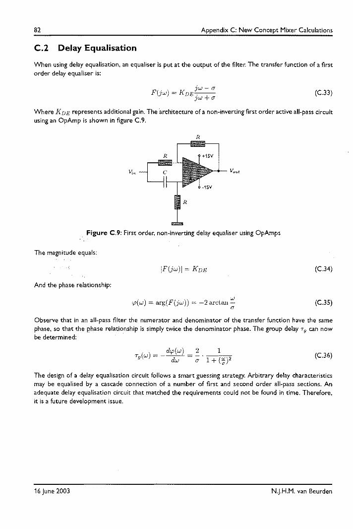
82 Appendix C: New Concept Mixer Calculations
C.2 Delay Equalisation
When using delay equalisation. an equaliser is put at the output of the filter. The transfer function of a first order delay equaliser is:
jw-a F(jw) = KDE-.-
Jw+a (C.33)
Where KDE represents additional gain. The architecture of a non-inverting first order active all-pass circuit using an OpAmp is shown in figure C.9.
R
Figure C.9: First order, non-inverting delay equaliser using OpAmps
The magnitude equals:
And the phase relationship:
IF (jw) I =
cp(w) = arg(F(jw)) = -2 arctan::: a
(C.34)
(C.35)
Observe that in an all-pass filter the numerator and denominator of the transfer function have the same phase. so that the p'hase relationship is simply twice the denominator phase. The group delay 7 g can now be determined:
2 1 -;; . 1 + (;;:)2 (C.36)
The design of a delay equalisation circuit follows a smart guessing strategy. Arbitrary delay characteristics may be equalised by a cascade connection of a number of first and second order all-pass sections. An adequate delay equalisation circuit that matched the requirements could not be found in time. Therefore. it is a future development issue.
16 June 2003 N.J.H.M. van Beurden

List Of Figures
List Of Figures
1.1
1.2 1.3
Schematic diagrams of CD, DVD and Blu-ray Disc systems 1.1.a CD ......... _ ...... _ .... ___ ............ _ ...... _ ......... _ ............... _ ..................... . 1.1.b DVD .......................................... . 1.1.c Blu-ray Disc ......... ... ..... . Embodiment of a audio CD data recovery circuit .. _.. Optical storage trends as a function of their perceived data rate
2.1 PLL architecture in time domain 2.2 sin( Be) ::::: Be if Be is sufficiently small 2.3 PLL architecture in the Laplace domain 2.4 Various types of PLLs
3.1 3.2 3.3 3.4 3.5 3.6 3.7
2.4.a Linear PLL 2.4.b Digital PLL 2.4.c All-Digital PLL
The prototype with cabinet, cards and computer Bus controller architecture Extension board layout Firmware generation overview Control software basic dialog Software platform overview Parameter editor dialog .............................._. 3.7.a Tab one: Parameter properties 3.7.b Tab two: Value names 3.7.c Tab three: Actions 3.7.d Tab four: General settings
High-level architecture of the implemented conventional concept ADPLL Zero-crossing approximation using linear interpolation Phase detector architecture First loop filter
83
2 5
9
11 12 13 13 13 13
15 16 17 18 19 20 21 21 21 21 21
23 24 25 26
4.1 4.2 4.3 4.4 4.5 4.6 4.7 4.8 4.9 4.10 4.11
Second loop filter Nominal frequency adder
........................................................ _ ..... _ 27
Discrete Timing Oscillator architecture Bit detection principle DTO interpolation .... ........... _._ .............................. _ .. _. Conventional concept control software dialog Screenshots of several measurement results using loop filter one 4.11.a Input signal (sine) and detected zero-crossings (peaks) 4.11.b Response to a phase step applied to loop filter one ... __ ..... ___ ....... _
27 28 28 29 30 32 32 32
4.11.c Input signal (sine) with loop filter output (bottom) and phase error (middle) staying zero 32 4.11.d Input signal (sine) with loop filter output (top) and phase error (middle) remaining zero 32
4.12
4.13
More measurement results using the first loop filter .... ... 33 33 4.12.a Input signal (sine wave) and DTO output (triangular wave), locked to the zero-crossings
4.12.b Frequency adjustment.. 33 Second loop filter measurements 34
N.J.H.M. van Beurden 16 June 2003

84 List Of Figures
4.13.a Step response for the second loop filter with input frequency of 4 kHz and frequency of 32 kHz
4.13.b Step response for the second loop filter with input frequency of 4 kHz and frequency of 128 kHz
5.1 New ADPLL Concept 5.2 Mixer architecture 5.3 OpAmp cascade 5.4 Multiple DTO bit detection architecture 5.5 Examples of multiple DTO method to discard bits
5.5.a Example one 5.5.b Example two
5.6 First embodiment of Multiple Clock-Phase ADPLL 5.7 Second embodiment of Multiple Clock-Phase ADPLL
6.1 Simulation flow 6.2 Simulator graphical user interface 6.3 Thresholded phase detection principle 6.4 Phase error for phase step
6.4.a Phase error for non-thresholded phase detector, for run length 4 signal 6.4.b Phase error for thresholded phase detector, for runlength 4 signal 6.4.c Phase error for non-thresholded phase detector, for Blu-ray Disc signal 6.4.d Phase error for thresholded phase detector, for Blu-ray Disc signal
6.5 Frequency step applied to run length 4 sequence 6.6 Mixer summator/integrator outputs for different input signals
6.6.a Mixer summator/integrator output with runlength 2 series (MatLab) 6.6.b Mixer summator/integrator output with Blu-ray Disc input signal (MatLab) 6.6.c Mixer summator/integrator Cgap output with run length 2 series 6.6.d Mixer summator/integrator practical measurement with runlength 2 series 6.6.e Mixer summator/integrator practical measurement with CD signal
6.7 Mixer filter outputs for different input signals 6.7.a Mixer filter output with runlength 2 series (MatLab) 6.7.b Mixer filter output with Blu-ray Disc input signal (MatLab) 6.7.c Mixer filter Cgap output with runlength 2 series .... 6.7.d Mixer flIter practical measurement with runlength 2 series 6.7.e Mixer filter practical measurement with CD signal
6.8 Mixer output plots 6.8.a Mixer output with runlength 2 series._._ 6.8.b Mixer output with Blu-ray Disc input signal 6.8.c Mixer output Cgap output with runlength 2 series 6.8.d Mixer output practical measurement with runlength 2 series 6.8.e Mixer output practical measurement with CD signal
6.9 Phase error responses ________________ _ 6.9.a Phase error for Blu-ray Disc signal without thresholded phase detection 6.9.b Phase error for Blu-ray Disc signal with thresholded phase detection 6.9.c Phase error for CD signal without thresholded phase detection 6.9.d Phase error for CD signal with threshold
6.10 Slopes ofthe DTO and AID convertor. __
A.1 Model in z-domain of implemented ADPLL
clock 34
clock 34
35 37 38 42 43 43 43 44 45
47 48 50 52 52 52 52 52 53 54 54 54 54 54 54 55 55 55 55 55 55 56 56 56 56 56 56 57 57 57 57 57 58
65
16 June 2003 N.J.H.M. van Beurden

List Of Figures
A2 Open loop transfer function of loop filter A3 Open loop transfer function of total PLL A4 Overshoot in percents depending on damping factor ( A5 Settling time determination via step response within 2% of final value (dotted lines)
C.1 Mixer filter implementation C.2 Mixer filter phase relationship C.3 Fourier approximation of a sawtooth signal with a various number of harmonics
C.3.a 1 harmonics C.3.b 2 harmonics __ _
C.3.c 10 harmonics C.4 Group delay 7 g of the original mixer low-pass filter C.5 Sallen-Key active low-pass filter circuit C.6 Bode diagrams of determined filter transfer function _ _________ __
C.6.a Magnitude plot (dB)_ C.6.b Phase plot (linear)
C.7 Group delay for the Bessel-Thomson polynomial low-pass filter C.8 Fourth order Bessel-Thomson filter with Sallen-Key architecture C.9 First order, non-inverting delay equaliser using OpAmps
N.J.H.M. van Beurden
85
65 66 69 71
75 75 76 76 76 76 77 78 79 79 79 80 80 82
16 June 2003

Glossary
Glossary
Nomenclature & Notational Conventions
We
Wi
Wo
Tg
Be Bi Bo .6.wH .6.wL .6.wPI .6.wPo
'P ( bit Cl C2 e(t) fbit
fCl
ic2 fe(t)
fm(t)
fnyq
f..(t)
fsys
KI Kp Kv Keo Kpd
m(t) m[nTc11 N<p NC2
NDTO Nnom
Npd ORlf,f ORlj,p ORpd OS p[nTcll
Wavelength Radial free running frequency Radial input frequency Radial output frequency Group delay Phase error Input phase Output phase PLL Hold range PLL Lock range PLL Pull-In range PLL Pull-Out range Argument I phase relationship Overshoot Channel bit signal Down-sampled system dock signal System clock signal Equaliser output signal Channel bit frequency Down-sampled system dock frequency System clock frequency Equaliser output frequency Mixer output frequency Nyquist frequency Slicer output frequency System dock frequency Loop filter proportional gain Loop filter proportional gain DC loop gain Controlled Oscillator gain Phase detector gain Mixer output signal Quantised mixer output signal Number of phase levels for Multiple Clock-Phase method Clock divider factor Number of bits used for the DTO Nominal frequency step Phase detector resolution Output Range of proportional part of the loop filter Output Range of integrating part of the loop filter Output Range of phase detector Oversampling factor DTO output signal
N.J.H.M. van Beurden
87
m rad/sec rad/sec rad/sec
sec rad rad rad
rad/sec rad/sec rad/sec rad/sec
Hz Hz Hz Hz Hz Hz Hz
radN·sec V/rad
bits bits
16 June 2003

88
s(t) sys Ts Tbit
TCl
TC2
Tm(t) %05
Slicer output signal System clock signal Settling time Channel bit period Down-sampled system clock period System clock period Mixer output period Overshoot in percent
Abbreviations & Acronyms
(AD)PLL AID ADPLL ASCII BD BDU BER CCO CD CD-R CD-ROM CD-RW CIRC CO DIA DC DCO DPLL DTO DVD DVD+R DVD+RW DVD-ROM ECC EEPLD EFM FIFO GUI HD HF 1/0 151 JUB LED LF LPF LPLL LSB
16 June 2003
(All-Digital or Digital) Phase-Locked Loop Analogue-to-Digital All-Digital Phase-Locked Loop American Standard Code for Information Interchange Blu-ray Disc Bit Decision Unit Bit Error Rate Current Controlled Oscillator Compact Disc Compact Disc Recordable Compact Disc Read-Only Memory Compact Disc Re-Writable Cross-Interleaved Reed-Solomon Code Controlled Oscillator Digital-to-Analogue Direct Current Discrete Controlled Oscillator I Digital Controlled Oscillator (Classical) Digital Phase-Locked Loop Discrete Timing Oscillator Digital Versatile Disc Digital Versatile Disc Recordable Digital Versatile Disc Re-Writable Digital Versatile Disc Read-Only Memory Error Correction Coding Erasable Electrical Programmable Logic Device Eight-to-Fourteen Modulation First In First Out Graphical User Interface Hard-Disc High-Frequency Input/Output Inter-Symbol Interference Joost Universal Bus Light-Emitting Diode Loop Filter Low-Pass Filter Linear Phase-Locked Loop Least Significant Bit
Glossary
sec sec sec sec sec %
N.J.H.M. van Beurden
Glossary
MO MSB MTF NA NCO NRZ NRZI OpAmp PAM PCB PO PLL PPM PWM RDS RLL SPLL SRAM VCO VHDL ZOH
Magneto Optical Most Significant Bit Modulation Transfer Function Numerical Aperture Numeric Controlled Oscillator Non-Return to Zero Non-Return to Zero Inverted Operational Amplifier Pulse Amplitude Modulation Printed Circuit Board Phase Detector Phase-Locked Loop Pulse Position Modulation Pulse Width Modulation Running Digital Sum Runlength-limited Code Software Phase-Locked Loop Static Random-Access Memory Voltage Controlled Oscillator Very High-Speed Integrated Circuit Hardware Description Language (VHSIC HDL) Zero-Order Hold
89
N.J.H.M. van Beurden 16 June 2003

Curriculum Vitae 91
Curriculum Vitae
N.J.H.M. van Beurden was born on the 21st of Februari 1979 in Tilburg (Noord-Brabant), the Netherlands. From 1991 till 1996 he attended secondary school (HA'l.O.) at "Mill Hill College" in Goirle. In 1996 he went to college at the Fontys Hogescholen Eindhoven (H.T.S.) from which he graduated in 1999 and got a Bachelor degree (Ing.) in Electronic & Electrical Engineering. His trainee work was carried out at Philips Research Laboratories Eindhoven, group Optics, and involved writing software for a Viterbi bitdetector prototype for high-speed optical discs. The graduation work at Philips Centre for Industrial Technology involved modelling and writing hardware description code for a generic wobble generator for Compact Disc and Digital Versatile Disc formatters. From 2000 till 2003 he studied information technology at the Eindhoven University of Technology,
receiving a Master of Science degree (lr.) in Electronic & Electrical Engineering. His graduation work was carried out under the supervision of the group "Computers, Networks and Design" of Prof. Ir. M.P.J. Stevens. It involved the modelling, simulation and practical development of a new high-speed all-digital phase-locked loop for optical recording. This work was carried out at the Philips Research Laboratories Eindhoven, group Storage Signal Processing.
N.J.H.M. van Beurden 16 June 2003