(el-486) for b.e(el) · pdf filevlsi design is a modular ... emphasis is on the implementation...
TRANSCRIPT

PRACTICAL WORK BOOK For Academic Session 2010
VLSI DESIGN (EL-486) For B.E(EL)
Name: Roll Number: Batch: Department:
Year:
Department of Electronic Engineering
N.E.D University of Engineering & Technology, Karachi-75270, Pakistan

- 2-
LABORATORY WORK BOOK FOR THE COURSE EL-486 VLSI DESIGN
Prepared By:
Engr. Hashim Raza Khan (Assistant Professor) Engr. Syed Riaz un Nabi (Assistant Professor)
Reviewed By:
Mr. Muhammad Khurram Shaikh (Assistant Professor)
Approved By:
The Board of Studies of Department of Electronic Engineering

- 3-
VLSI design is a modular methodology for saving microchip area by minimizing the interconnect fabrics and to increase circuit efficiency in terms of complexity of circuit, power consumption and frequency response associated to the design. The aim of this workbook is to familiarize the students with tools used in the field of VLSI design. All Lab Tasks are mostly targeting towards standardized tools like Cadence, Microwind, Quartus and Modelsim. The workbook has two sections: the first one is directed towards modeling and simulation of digital circuits using Cadence and Microwind. Starting five Lab Tasks are related to first section. In the second section, the emphasis is on the implementation of digital circuits on FPGA boards by using Verilog HDL. Last four tasks are reserved for this section. By acquiring knowledge of these tasks and related tools, Students will be capable of designing, simulating and verifying VLSI Design.

- 4-
VLSI Design Laboratory CONTENTS
Lab# Lab Objectives Page# Remarks
1 To determine the behavior of MOS transistor using Cadence by analyzing its
• ID v/s VDS curve • ID v/s VGS curve • Early Effect
5
2 To determine the behavior of following circuits by Modeling and Simulating them:
• A CMOS Inverter • A Common Source Amplifier
8
3 To determine the gate capacitance of NMOS transistor and determine its dependence on the width of the transistor.
12
4 To draw the layout of the CMOS inverter. 15 5 To draw the layout of a Current Mirror. 17 6 • To understand 4 to 1 Mux working principle
• To understand Quartus-II Software for Development of Verilog HDL Codes
• To implement & test 4 to 1 Mux on Verilog HDL
19
7 • To understand 4-bit BCD counter and BCD to Seven Segment Decoder
• To understand Quartus-II Software for Development of Verilog HDL Codes
• To implement & test 4-bit BCD counter on Verilog HDL
24
8 • To understand 4-bit Full Adder Working principle
• To understand Quartus-II Software for Development of Verilog HDL Codes
• To implement & test 4-bit Full Adder on Verilog HDL
• To verify Adder working on DE2 Boards
29
9
To develop a self selected Lab project based on Hardware Implementation of particular topic on DE2 Board.
33

VLSI Design Lab Session 01 NED University of Engineering and Technology, Department of Electronic Engineering
- 5-
Lab No. 1
Objective: To determine the behavior of MOS transistor using Cadence by analyzing its
• ID v/s VDS curve • ID v/s VGS curve • Early Effect
Equipment Required:
• Linux & Cadence Installed PCs
Theory:
The physical operation of a MOSFET can be divided into three regions of operation. For small value of VG the transistor is switched off. As VGS increases from zero, holes in the p-substrate under the gate are repelled. Thus a depletion region is created from drain to source. For a sufficient value of interface potential, electron from source can actually travel through interface to drain terminal. The value of interface potential at this stage is called “Threshold Voltage” (VTH). When VGS > Vth and VDS < ( VGS - Vth ): Triode of Linear Region In this region of operation MOSFET operates like a resistor, controlled by the gate voltage relative to both the source and drain voltages. The current from drain to source is modeled as:
where μn is the charge-carrier effective mobility, W is the gate width, L is the gate length and Cox is the gate oxide capacitance per unit area. When VGS > Vth and VDS > ( VGS - Vth ): Saturation Region The switch is turned on, and a channel has been created, which allows current to flow between the drain and source. Since the drain voltage is higher than the gate voltage, the electrons spread out, and conduction is not through a narrow channel but through a broader, two- or three-dimensional current distribution extending away from the interface

VLSI Design Lab Session 01 NED University of Engineering and Technology, Department of Electronic Engineering
- 6-
and deeper in the substrate. The onset of this region is also known as pinch-off to indicate the lack of channel region near the drain. The drain current is now weakly dependent upon drain voltage and controlled primarily by the gate–source voltage, and modeled very approximately as:
ID v/s VDS curve for different values of Vgs
ID v/s VDS curve

VLSI Design Lab Session 01 NED University of Engineering and Technology, Department of Electronic Engineering
- 7-
The characteristic curve of Fig. 1 indicates three regions of operation. The cutoff region, the triode region and the saturation region. The device is cutoff when VGS < vt whereas it follows a linear relationship in triode region. The MOS operation, therefore, can be modeled as a linear resistor in triode region. Saturation region on the other hand is used when MOS is employed as an amplifier. In saturation region MOS provides a drain current which is independent of VDS and is determined by VGS according to a square law relationship. Thus Fig. 2 shows MOSFET operation as an ideal current source whose value is controlled by VGS. EARLY EFFECT: When the MOS operated in the saturation region, practical MOS shows some dependence of the drain current on the drain source voltage at a constant VGS. That dependency is almost linear with a slope equal 1/ro. When extrapolated the curves, the characteristics lines meet at a point on the VDS axis at VDS = VA. The voltage VA is called the early voltage. This phenomenon is generated because of the reduction in the effective channel width due to the increase in the reverse-bias voltage on the drain-bulk junction.
Procedure:
Follow the instructions given during Lab to complete task successfully. Results:

VLSI Design Lab Session 02 NED University of Engineering and Technology, Department of Electronic Engineering
- 8-
Lab No. 2
Objective: To determine the behavior of following circuits by Modeling and simulating them:
• A CMOS inverter. • A Common Source Amplifier.
Equipment Required:
• Linux & Cadence Installed PCs
Theory:
CMOS INVERTER:
A CMOS Inverter
An inverter circuit outputs a voltage representing the opposite logic-level to its input. Inverters can be constructed using a single NMOS transistor or a single PMOS transistor coupled with a resistor. Since this 'resistive-drain' approach uses only a single type of transistor, it can be fabricated at low cost. However, because current flows through the
VLSI Design Lab Session 02 NED University of Engineering and Technology, Department of Electronic Engineering
- 9-
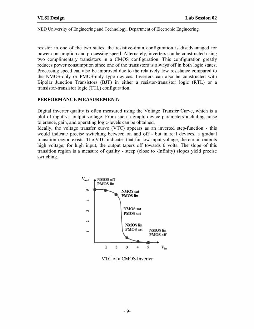
resistor in one of the two states, the resistive-drain configuration is disadvantaged for power consumption and processing speed. Alternately, inverters can be constructed using two complimentary transistors in a CMOS configuration. This configuration greatly reduces power consumption since one of the transistors is always off in both logic states. Processing speed can also be improved due to the relatively low resistance compared to the NMOS-only or PMOS-only type devices. Inverters can also be constructed with Bipolar Junction Transistors (BJT) in either a resistor-transistor logic (RTL) or a transistor-transistor logic (TTL) configuration. PERFORMANCE MEASUREMENT: Digital inverter quality is often measured using the Voltage Transfer Curve, which is a plot of input vs. output voltage. From such a graph, device parameters including noise tolerance, gain, and operating logic-levels can be obtained. Ideally, the voltage transfer curve (VTC) appears as an inverted step-function - this would indicate precise switching between on and off - but in real devices, a gradual transition region exists. The VTC indicates that for low input voltage, the circuit outputs high voltage; for high input, the output tapers off towards 0 volts. The slope of this transition region is a measure of quality - steep (close to -Infinity) slopes yield precise switching.
VTC of a CMOS Inverter
VLSI Design Lab Session 02 NED University of Engineering and Technology, Department of Electronic Engineering
- 10-
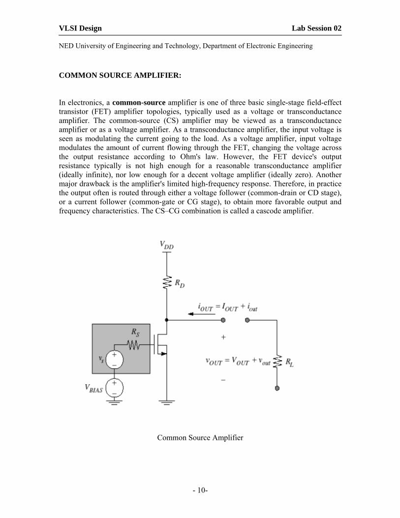
COMMON SOURCE AMPLIFIER:
In electronics, a common-source amplifier is one of three basic single-stage field-effect transistor (FET) amplifier topologies, typically used as a voltage or transconductance amplifier. The common-source (CS) amplifier may be viewed as a transconductance amplifier or as a voltage amplifier. As a transconductance amplifier, the input voltage is seen as modulating the current going to the load. As a voltage amplifier, input voltage modulates the amount of current flowing through the FET, changing the voltage across the output resistance according to Ohm's law. However, the FET device's output resistance typically is not high enough for a reasonable transconductance amplifier (ideally infinite), nor low enough for a decent voltage amplifier (ideally zero). Another major drawback is the amplifier's limited high-frequency response. Therefore, in practice the output often is routed through either a voltage follower (common-drain or CD stage), or a current follower (common-gate or CG stage), to obtain more favorable output and frequency characteristics. The CS–CG combination is called a cascode amplifier.
Common Source Amplifier

VLSI Design Lab Session 02 NED University of Engineering and Technology, Department of Electronic Engineering
- 11-
Procedure:
Follow the instructions given during Lab to complete task successfully. Results:
VLSI Design Lab Session 03 NED University of Engineering and Technology, Department of Electronic Engineering
- 12-
Lab No. 3
Objective: To determine the gate capacitance of NMOS transistor and to determine its dependence on the width of the transistor.
Equipment Required:
• Linux & Cadence Installed PCs
Theory:
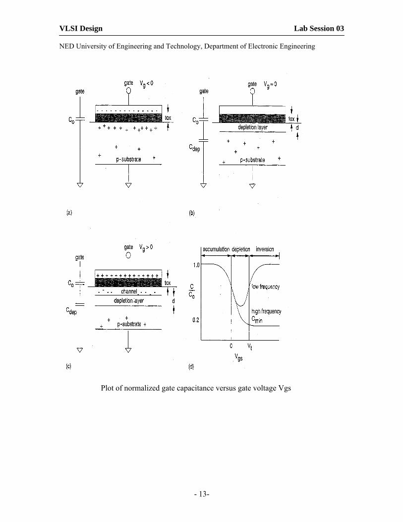
The gate of the MOS transistor is isolated from the conducting channel by the gate oxide that has a capacitance per unit area equal to Cox = εox / tox. The total value of this capacitance is called the gate capacitance Cg. Because of the lateral diffusion, inherit in transistors, the effective channel of the transistor L becomes shorter than the length the transistor was originally designed for. It also gives rise to a parasitic capacitance between gate and source (drain) that is called the overlap capacitance.This capacitance is strictly linear and has a fixed value. the most significant MOS parasitic circuit element, the gate-to-channel capacitance CGC varies in both magnitude and in its division into three components CGCS, CGCD, and CGCB (being the gate-to-source, gate-to-drain, and gate-to-body capacitances, respectively), depending upon the operation region and terminal voltages. MOS gate oxide capacitance can be divided into three regions: Accumulation occurs when Vg is negative (for P material). Holes are induced under the oxide. Depletion occurs when Vg is near zero but < Vtn. Here the Cgate is given by Cox*A in series with depletion layer capacitance Cdep. Inversion occurs when Vg is positive and > Vtn (for P material). A model for inversion is comprised of Cox*A connecting from gate-to-channel and Cdep connecting from channel-to-substrate.
VLSI Design Lab Session 03 NED University of Engineering and Technology, Department of Electronic Engineering
- 13-
Plot of normalized gate capacitance versus gate voltage Vgs

VLSI Design Lab Session 03 NED University of Engineering and Technology, Department of Electronic Engineering
- 14-
Procedure:
Follow the instructions given during Lab to complete task successfully. Results:

VLSI Design Lab Session 04 NED University of Engineering and Technology, Department of Electronic Engineering
- 15-
Lab No. 4
Objective:
To draw the layout of the CMOS inverter. Equipment Required:
• Microwind, Linux & Cadence Installed PCs Theory: Following figure is showing schematic of CMOS Inverter.
CMOS Inverter
CMOS Inverter consists of a pair of NMOS and PMOS transistors. CMOS Inverter is a basic and easy digital circuit to learn so it is selected for understanding development of Lay out. Two different transistors have to be placed in Lay out so it will be a good exercise for learning structure of both transistors. Following figure is showing Lay out diagram of the Inverter.

VLSI Design Lab Session 04 NED University of Engineering and Technology, Department of Electronic Engineering
- 16-
CMOS Inverter Lay out
Procedure:
Follow the instructions given during Lab to complete task successfully. Results:

LSI Design Lab Session 05 NED University of Engineering and Technology, Department of Electronic Engineering
- 17-
Lab No. 5
Objective:
To draw the layout of a Current Mirror. Equipment Required:
• Microwind, Linux & Cadence Installed PCs Theory:
A current mirror is a circuit designed to copy a current through one active device by controlling the current in another active device of a circuit, keeping the output current constant regardless of loading. Conceptually, an ideal current mirror is simply an ideal current amplifier. The current mirror is used to provide bias currents and active loads to circuits. Following figure is showing a MOS Current Mirror.
MOS Current Mirror In order to mirror the current at the drain of Q2, a reference current is to be generated. The corresponding output current generated is given as:

LSI Design Lab Session 05 NED University of Engineering and Technology, Department of Electronic Engineering
- 18-
It can be seen that the ratio of the two currents is a function of device dimensions: a property that can be controlled at the time of device modeling.
Procedure:
Follow the instructions given during Lab to complete task successfully. Results:
LSI Design Lab Session 06 NED University of Engineering and Technology, Department of Electronic Engineering
- 19-
Lab No. 6
Objective: • To understand 4 to 1 Mux Working principle • To understand Quartus-II Software for Development of Verilog HDL Codes • To implement & test 4 to 1 Mux on Verilog HDL by
1. Gate Level Modeling 2. Data Flow Modeling 3. Behavioral Modeling
Equipment Required:
• Quartus-II & Modelsim Installed PCs
Theory:
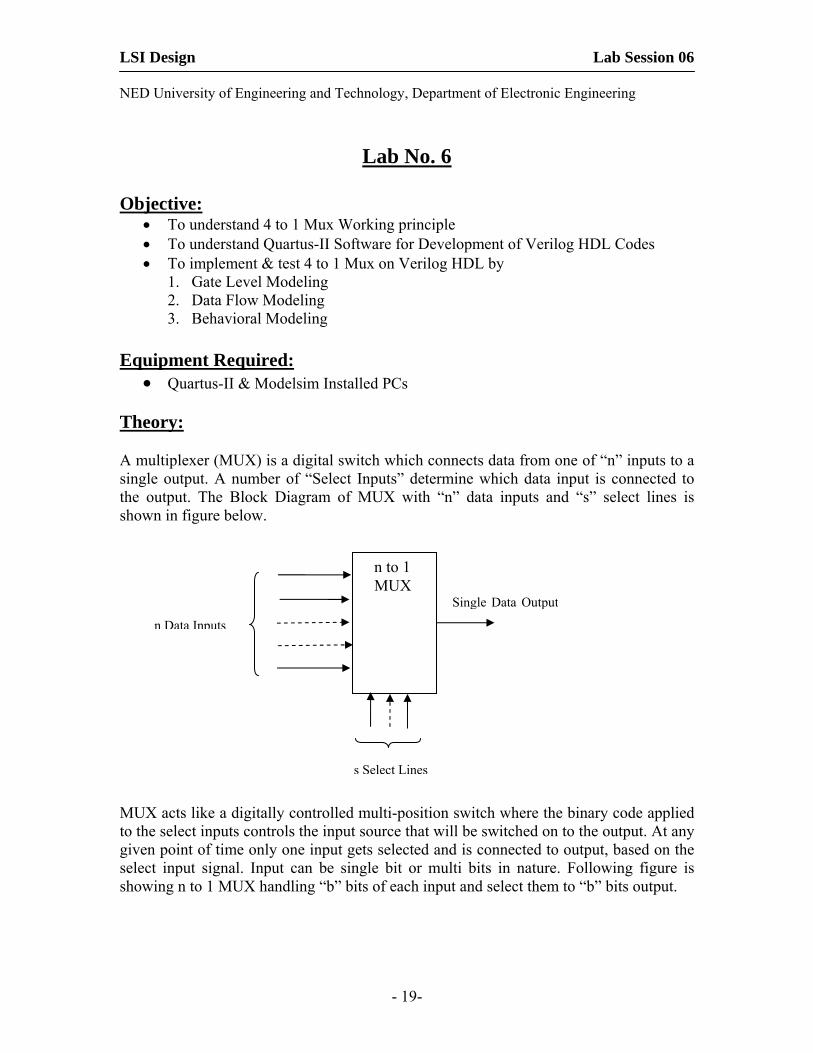
A multiplexer (MUX) is a digital switch which connects data from one of “n” inputs to a single output. A number of “Select Inputs” determine which data input is connected to the output. The Block Diagram of MUX with “n” data inputs and “s” select lines is shown in figure below.
MUX acts like a digitally controlled multi-position switch where the binary code applied to the select inputs controls the input source that will be switched on to the output. At any given point of time only one input gets selected and is connected to output, based on the select input signal. Input can be single bit or multi bits in nature. Following figure is showing n to 1 MUX handling “b” bits of each input and select them to “b” bits output.
n to 1 MUX
n Data Inputs
s Select Lines
Single Data Output

LSI Design Lab Session 06 NED University of Engineering and Technology, Department of Electronic Engineering
- 20-
A 4 to 1 MUX is shown in figure below. There are total of 4 input lines I0 to I3 are present and two selection lines S0 and S1 are decoded to select a particular input to appear at output.
The truth table for the 4:1 MUX is given in the table below.
S1 S0 Output 0 0 I0 0 1 I1 1 0 I2 1 1 I3
Procedure:
4 to 1 MUX I0
S1 S0
Single Data OutputI1
I2
I3
n to 1 MUX
b-bits Data Inputs (Total n inputs)
s Select Lines
b-bits Data Output

LSI Design Lab Session 06 NED University of Engineering and Technology, Department of Electronic Engineering
- 21-
1. Understand Gate level Modeling code provided here. 2. Create new Quartus-II project for editing the code. 3. Open new Verilog file and edit given code in it. 4. Include Verilog file in your project and compile your project. 5. Open Modelsim and simulate your project and verify results. 6. Understand Data flow Modeling code provided here. 7. Repeat steps 3 to 5. 8. Understand Behavioral Modeling code provided here. 9. Repeat steps 3 to 5.
Gate Level Verilog Code:
// Module 4-to-1 multiplexer using gate level modelling.
module mux4_to_1 (output out,
input i0, i1, i2, i3,
input s1, s0);
// Internal wire declarations
wire s1n, s0n;
wire y0, y1, y2, y3;
// Gate instantiations
// Create s1n and s0n signals.
not (s1n, s1);
not (s0n, s0);
// 3-input and gates instantiated
and (y0, i0, s1n, s0n);
and (y1, i1, s1n, s0);

LSI Design Lab Session 06 NED University of Engineering and Technology, Department of Electronic Engineering
- 22-
and (y2, i2, s1, s0n);
and (y3, i3, s1, s0);
// 4-input or gate instantiated
or (out, y0, y1, y2, y3);
endmodule
Data Flow Verilog Code:
// Module 4-to-1 multiplexer using data-flow modelling.
module mux4_to_1 ( output out,
input i0, i1, i2, i3,
input s1, s0);
//Logic equation for out
assign out = (~s1 & ~s0 & i0)|
(~s1 & s0 & i1) |
(s1 & ~s0 & i2) |
(s1 & s0 & i3) ;
endmodule
Behavioral Verilog Code:
// Module 4-to-1 multiplexer using behavioral modelling.
module mux4_to_1 ( output out,

LSI Design Lab Session 06 NED University of Engineering and Technology, Department of Electronic Engineering
- 23-
input i0, i1, i2, i3,
input s1, s0);
always @(s1 or s0 or i0 or i1 or i2 or i3)
begin
case ({s1, s0})
2'b00: out = i0;
2'b01: out = i1;
2'b10: out = i2;
2'b11: out = i3;
default: out = 1'bx;
endcase
end
endmodule
Results:
VLSI Design Lab Session 07 NED University of Engineering and Technology, Department of Electronic Engineering
- 24-
Lab No. 7
Objective:
• To understand 4-bit BCD counter and BCD to Seven Segment Decoder • To understand Quartus-II Software for Development of Verilog HDL Codes • To implement & test 4-bit BCD counter on Verilog HDL by Behavioral Modeling
Equipment Required:
• Quartus-II & Modelsim Installed PCs
Theory:
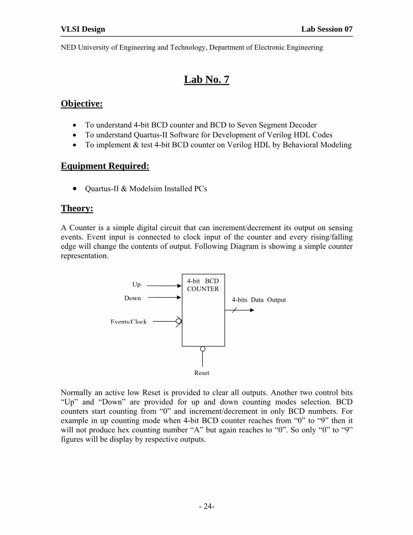
A Counter is a simple digital circuit that can increment/decrement its output on sensing events. Event input is connected to clock input of the counter and every rising/falling edge will change the contents of output. Following Diagram is showing a simple counter representation.
Normally an active low Reset is provided to clear all outputs. Another two control bits “Up” and “Down” are provided for up and down counting modes selection. BCD counters start counting from “0” and increment/decrement in only BCD numbers. For example in up counting mode when 4-bit BCD counter reaches from “0” to “9” then it will not produce hex counting number “A” but again reaches to “0”. So only “0” to “9” figures will be display by respective outputs.
4-bit BCD COUNTER
Up
Reset
4-bits Data OutputDown
Events/Clock
VLSI Design Lab Session 07 NED University of Engineering and Technology, Department of Electronic Engineering
- 25-
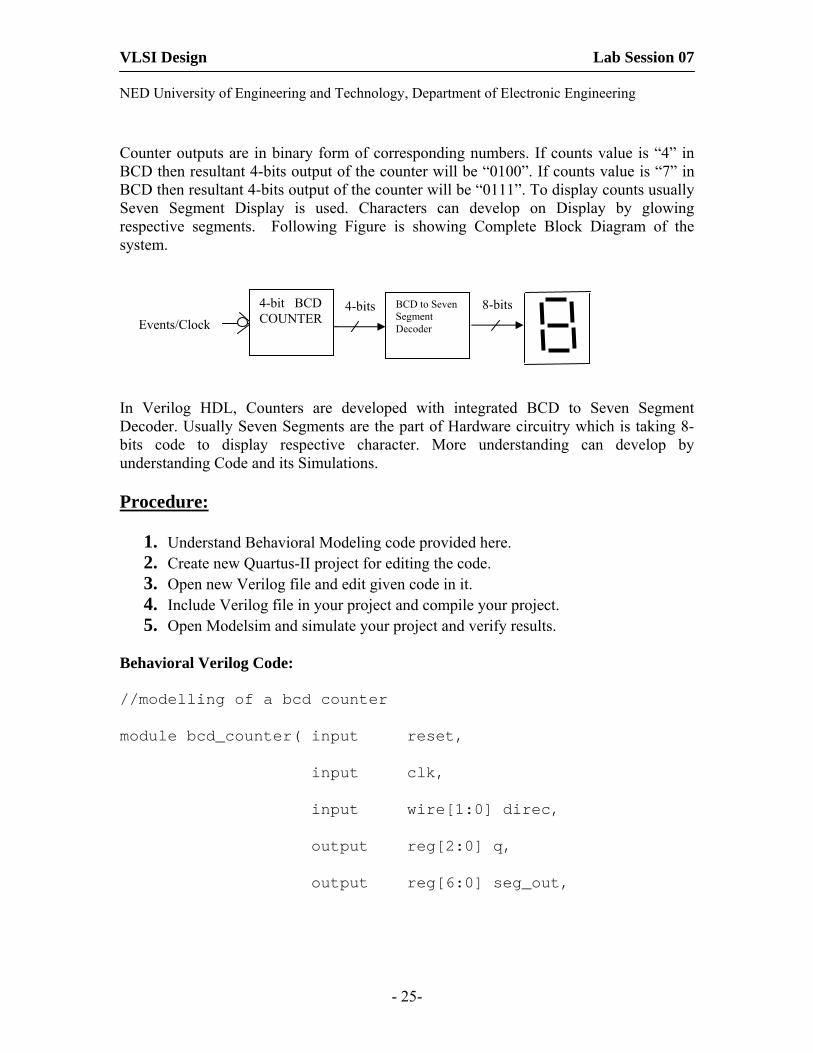
Counter outputs are in binary form of corresponding numbers. If counts value is “4” in BCD then resultant 4-bits output of the counter will be “0100”. If counts value is “7” in BCD then resultant 4-bits output of the counter will be “0111”. To display counts usually Seven Segment Display is used. Characters can develop on Display by glowing respective segments. Following Figure is showing Complete Block Diagram of the system.
In Verilog HDL, Counters are developed with integrated BCD to Seven Segment Decoder. Usually Seven Segments are the part of Hardware circuitry which is taking 8-bits code to display respective character. More understanding can develop by understanding Code and its Simulations.
Procedure:
1. Understand Behavioral Modeling code provided here. 2. Create new Quartus-II project for editing the code. 3. Open new Verilog file and edit given code in it. 4. Include Verilog file in your project and compile your project. 5. Open Modelsim and simulate your project and verify results.
Behavioral Verilog Code:
//modelling of a bcd counter
module bcd_counter( input reset,
input clk,
input wire[1:0] direc,
output reg[2:0] q,
output reg[6:0] seg_out,
4-bit BCD COUNTER
4-bitsEvents/Clock
BCD to Seven Segment Decoder
8-bits
VLSI Design Lab Session 07 NED University of Engineering and Technology, Department of Electronic Engineering
- 26-
output reg clk2
);
// clock divider circuitry
reg [7:0] counter;
always @ (posedge clk) begin
if (reset)
counter <= 8'b0;
else if (counter == 8'd127)
counter <= 8'b0;
else
counter <= counter + 1'b1;
end
always @ (posedge clk) begin
if (reset)
clk2 <= 1'b0;
else if (counter == 8'd127)
clk2 <= ~clk2;
end
// body of bcd counter
always @ (posedge clk) begin
if (reset) begin

VLSI Design Lab Session 07 NED University of Engineering and Technology, Department of Electronic Engineering
- 27-
q <= 3'b0;
end
else if (counter == 8'd127) begin
//q = q + 1;
case (direc)
//00 : q = q;
2'b01 : q <= q + 1;
2'b10 : q <= q - 1;
default : q <= q;
endcase
end
end
always @ (posedge clk) begin
case (q)
2'd0 : seg_out <= 7'b_1000_000;
2'd1 : seg_out <= 7'b_1111_001;
2'd2 : seg_out <= 7'b_0100_100;
2'd3 : seg_out <= 7'b_0110_000;
2'd4 : seg_out <= 7'b_0011_001;
2'd5 : seg_out <= 7'b_0010_010;
2'd6 : seg_out <= 7'b_1000_010;

VLSI Design Lab Session 07 NED University of Engineering and Technology, Department of Electronic Engineering
- 28-
2'd7 : seg_out <= 7'b_1111_000;
Endcase
End
endmodule
Results:

VLSI Design Lab Session 08 NED University of Engineering and Technology, Department of Electronic Engineering
- 29-
Lab No. 8
Objective: • To understand 4-bit Full Adder Working principle • To understand Quartus-II Software for Development of Verilog HDL Codes • To implement & test 4-bit Full Adder on Verilog HDL by
1. Gate Level Modeling 2. Data Flow Modeling 3. Behavioral Modeling
• To verify Adder working on DE2 Boards
Equipment Required: • Quartus-II & Modelsim Installed PCs • DE2 Boards
Theory:
An Adder is a digital circuit that is utilized frequently in processors for Arithmetic operations. It is very basic and important part of ALU. Following figure is showing a simple 1-bit adder. Two 1-bit numbers are added with each other and then with Carry in bit and the result is generated at Single data bit with Carry out bit.
Full adders are developed for 1-bit to n-bits numbers. Common Adders are available with 4-bits, 8-bits and 16-bits input number ranges. Following Figure is showing a 4-bit Full Adder. Carry in and Carry out are always single bit irrespective of input number size.
4-bit Full Adder
First 4-bit Number 4-bit Data Output
Second 4-bit Number
Carry in Carry Out
1-bit Full Adder
First 1-bit Number Single bit Data Output
Second 1-bit Number
Carry in Carry Out

VLSI Design Lab Session 08 NED University of Engineering and Technology, Department of Electronic Engineering
- 30-
Procedure:
1. Understand Gate level Modeling code provided here. 2. Create new Quartus-II project for editing the code. 3. Open new Verilog file and edit given code in it. 4. Include Verilog file in your project and compile your project. 5. Open Modelsim and simulate your project and verify results. 6. Understand Data flow Modeling code provided here. 7. Repeat steps 3 to 5. 8. Understand Behavioral Modeling code provided here. 9. Repeat steps 3 to 5. 10. Connect DE2 Boards and setting switches as inputs. 11. Test your project on Hardware.
Gate Level Verilog Code:
// Define a 1-bit full adder
module fulladd(output sum,
output c_out,
input a,
input b,
input c_in);
// Internal nets
wire s1, c1, c2;
// Instantiate logic gate primitives
xor (s1, a, b);
and (c1, a, b);
xor (sum, s1, c_in);

VLSI Design Lab Session 08 NED University of Engineering and Technology, Department of Electronic Engineering
- 31-
and (c2, s1, c_in);
xor (c_out, c2, c1);
endmodule
Data Flow Level Verilog Code:
//4-bit fulladder using dataflow modelling.
module fulladd4(output [3:0] sum,
output c_out,
input [3:0] a,
input [3:0] b,
input c_in);
assign {c_out, sum} = a + b + c_in;
endmodule
Behavioral Level Verilog Code:
// Define a 4-bit full adder
module fulladd4(output [3:0] sum,
output c_out,
input [3:0] a,
input [3:0] b,
input c_in);
// Internal nets
wire c1, c2, c3;

VLSI Design Lab Session 08 NED University of Engineering and Technology, Department of Electronic Engineering
- 32-
// Instantiate four 1-bit full adders.
fulladd fa0(sum[0], c1, a[0], b[0], c_in);
fulladd fa1(sum[1], c2, a[1], b[1], c1);
fulladd fa2(sum[2], c3, a[2], b[2], c2);
fulladd fa3(sum[3], c_out, a[3], b[3], c3);
endmodule
Results:

VLSI Design Lab Session 09 NED University of Engineering and Technology, Department of Electronic Engineering
- 33-
Lab No. 9
Objective: To develop a self selected Lab project based on Hardware Implementation of particular topic on DE2 Board.
• To select Lab project after discussion with Course Teacher. • Implement and test Verilog Code related to project on Quartus-II and Modelsim. • Verify Hardware functioning of the project on DE2 Board.
Equipment Required:
• Quartus-II & Modelsim Installed PCs • DE2 Boards
Theory: All students should select different projects related to their interests or assigned by Course Teacher. Students can perform these tasks in groups. Maximum number of students in a group is restricted to five persons. Remaining matters related to project will discuss in class.
Procedure:
1. Identify selected project and the scope of the project. 2. Identify Group members associated to the project. 3. Develop Code and test simulation results on Modelsim. 4. Verify Hardware Implementation on DE2 Boards. 5. Submit a small report on project with workbook.
Results: