electrical compliance test specification enhanced ... · chapter 2: test descriptions 2 enhanced...
TRANSCRIPT

Enhanced SuperSpeed Electrical Compliance i
Electrical Compliance Test Specification Enhanced SuperSpeed Universal Serial Bus
Date: February 14, 2017
Revision: 1.0

ii Enhanced SuperSpeed Electrical Compliance
Copyright © 2017, USB 3.0 Promoter Group All rights reserved.
INTELLECTUAL PROPERTY DISCLAIMER
THIS SPECIFICATION IS PROVIDED TO YOU “AS IS” WITH NO WARRANTIES WHATSOEVER,
INCLUDING ANY WARRANTY OF MERCHANTABILITY, NON-INFRINGEMENT, OR FITNESS FOR
ANY PARTICULAR PURPOSE. THE AUTHORS OF THIS SPECIFICATION DISCLAIM ALL LIABILITY,
INCLUDING LIABILITY FOR INFRINGEMENT OF ANY PROPRIETARY RIGHTS, RELATING TO USE
OR IMPLEMENTATION OF INFORMATION IN THIS SPECIFICATION. THE PROVISION OF THIS
SPECIFICATION TO YOU DOES NOT PROVIDE YOU WITH ANY LICENSE, EXPRESS OR IMPLIED, BY
ESTOPPEL OR OTHERWISE, TO ANY INTELLECTUAL PROPERTY RIGHTS.
All product names are trademarks, registered trademarks, or service marks of their respective owners.

Scope of this Revision
This revision of the specification describes the testing to be applied to hardware based on the Universal Serial
Bus 3.1 Specification, revision 1.0.
This document is an intermediate draft for comment only and is subject to change without notice.
*Third-party brands and names are the property of their respective owners.
Significant Contributors:
Dan Froelich (author) Intel Jit Lim Keysight
Howard Heck (author) Intel Jim Mueller Teledyne Lecroy
John Stonick (co-author) Synopsys Carl Murdock Tektronix
David Bouse (co-author) Intel Manish Nilange Intel
Michael Andres Bitifeye / Keysight Gary Simonton Tektronix
Sourabh Das Tektronix Hermann Stehling Bitifeye / Keysight
Brian Fetz Keysight Jennifer Tsai Apple
Thorsten Goetzerlmann Keysight Randy White Tektronix
Lev Kolomiets Intel Yunyi Zhang Tektronix
Biing-Lin Lem Keysight

iv Enhanced SuperSpeed Electrical Compliance
Table of Contents
TABLE OF CONTENTS ........................................................................................... IV
1 INTRODUCTION ................................................................................................. 1
1.1 Related Documents ............................................................................................................................... 1
1.2 USB 2.0 Compliance ............................................................................................................................. 1
2 TEST DESCRIPTIONS ........................................................................................ 1 TD.1.1 Low Frequency Periodic Signaling TX Test. ................................................................................. 1 TD.1.2 Low Frequency Periodic Signaling RX Test. ................................................................................. 1 TD.1.3 Transmitted Eye Test at 5 GT/s ...................................................................................................... 2 TD.1.4 Transmitted Eye Test at 10 GT/s .................................................................................................... 4 TD.1.5 Transmit Equalization Test at 10 GT/s ........................................................................................... 5 TD.1.6 Transmitted SSC Profile Test at 5 GT/s ......................................................................................... 6 TD.1.7 Transmitted SSC Profile Test at 10 GT/s ....................................................................................... 7 TD.1.8 Receiver Jitter Tolerance Test at 5 GT/s......................................................................................... 8 TD.1.9 Receiver Jitter Tolerance Test at 5 GT/s (Type-C) ....................................................................... 10 TD.1.10 Receiver Jitter Tolerance Test at 10 GT/s ................................................................................. 12

Chapter 1: Introduction
Enhanced SuperSpeed Electrical Compliance 1
Introduction This document provides the compliance criteria and test descriptions for SuperSpeed USB
devices, hubs and host controllers that conform to the Universal Serial Bus 3.1 Specification, rev
1.0. It is relevant for anyone building SuperSpeed & SuperSpeedPlus USB hardware. These
criteria address the electrical requirements for a SuperSpeed & SuperSpeedPlus physical layer
design. Test descriptions provide a high level overview of the tests that are performed to check the
compliance criteria. The descriptions are provided with enough detail so that a reader can
understand what the test does. The descriptions do not describe the actual step-by-step procedure
to perform the test.
1.1 Related Documents
[1] Universal Serial Bus 3.0 Specification, revision 1.0, November 12, 2008
[2] Universal Serial Bus 3.1 Specification, revision 1.0, July 26, 2013
[3] Universal Serial Bus Specification, Revision 2.0, April 27, 2000.
[4] USB-IF USB 2.0 Electrical Test Specification, Version 1.03, January 2005.
1.2 USB 2.0 Compliance
USB 2,0 testing is required for USB 3.1 devices and is covered by a separate compliance testing program. Refer to
[3] and [4] for details.
2 Test Descriptions
TD.1.1 Low Frequency Periodic Signaling TX Test.
This test verifies that the low frequency periodic signal transmitter meets the timing requirements when
measured at the compliance test port.
Overview of Test Steps
1. The test performs the following steps. Connect the DUT to a simple breakout test fixture. Disconnect
bus power if the DUT is a bus powered device.
2. Power on the device under test (connect bus powered if DUT is a bus powered device) and let it pass
through the Rx.Detect state to the Polling.LFPS substate.
3. Trigger on the initial LFPS burst sent by the DUT and capture the first five bursts for analysis..
4. Measure the following LFPS parameters and compare against the USB 3.1 specification requirements:
tburst, trepeat, tperiod, tRiseFall2080, Duty cycle, VCM-AC-LFPS, and VTX-DIFF-PP-LFPS. For these
measurements the start of an LFPS burst is defined as starting when the absolute value of the differential
voltage has exceeded 100 mV and the end of an LFPS burst is defined as when the absolute value of the
differential voltage has been below 100 mV for 50 ns. tperiod, tRiseFall2080, Duty cycle, VCM-AC-LFPS,
and VTX-DIFF-PP-LFPS are only measured during the period from 100 nanoseconds after the burst start to 100
nanoseconds before the burst stop.
TD.1.2 Low Frequency Periodic Signaling RX Test.
This test verifies that the DUT low frequency periodic signal receiver recognizes LFPS signaling with voltage
swings and duty cycles that are at the limits of what the specification allows. The link test specification
includes test that vary additional LFPS parameters to test the LFPS receiver.
Overview of Test Steps

Chapter 2: Test Descriptions
Enhanced SuperSpeed Electrical Compliance 2
The test performs the following steps.
1. Connect the DUT to a simple breakout test fixture. Disconnect bus power if the DUT is a bus powered
device.
2. Power on the device under test (connect bus powered if DUT is a bus powered device) and let it pass
through the Rx.Detect state to the Polling.LFPS substate.
3. Trigger on the initial LFPS burst sent by the DUT and send LFPS signals to the DUT with the following
parameters:
a. tPeriod 50 ns.
b. VTX-DIFF-PP-LFPS 800 mV.
c. Duty Cycle 50%
4. The test passes if the device recognizes the LFPS and starts sending the TXEQ sequence.
5. The test is repeated with the following parameters:
a. tPeriod 50 ns, VTX-DIFF-PP-LFPS 1200 mV, Duty Cycle 50%.
b. tPeriod 50 ns, VTX-DIFF-PP-LFPS 1000 mV, Duty Cycle 40%.
c. tPeriod 50 ns, VTX-DIFF-PP-LFPS 1000 mV, Duty Cycle 60%.
TD.1.3 Transmitted Eye Test at 5 GT/s
This test verifies that the transmitter meets the eye width, deterministic jitter and random jitter requirements
when measured at the compliance test port with nominal transmitter equalization and after processing with
the appropriate channels and post processing as shown in Table 2-1.
Connector Type Channel Reference Equalizer
Std-A 3m Cable + 5” PCB
Long Channel
Std-B 3m Cable + 11” PCB Long Channel
Type-C (Host) Device Under Test >> USB 3.1 Host Fixture
1C >> SCOPE (Embed 7dB Cable +
Host/Device PCB)
SSGen1_TxComp12p7dB_Embedding.s4p
Long Channel
Type-C (Device) Device Under Test >> USB 3.1 Device
Fixture 1C >> SCOPE (Embed 7dB Cable +
Host/Device PCB)
SSGen1_TxComp12p7dB_Embedding.s4p
Long Channel
Micro-B 1m Cable + 11” PCB Long Channel
Micro-AB (Host Only) 1m Cable + 5” PCB + Micro-A to Std-A
Receptacle adapter
Long Channel
Micro-AB (DRD) 1m Cable + 11” PCB (device mode)
1m Cable + 5” PCB + Micro-A to Std-A
Receptacle adapter (host mode)
Long Channel
Chapter 2: Test Descriptions
Enhanced SuperSpeed Electrical Compliance 3
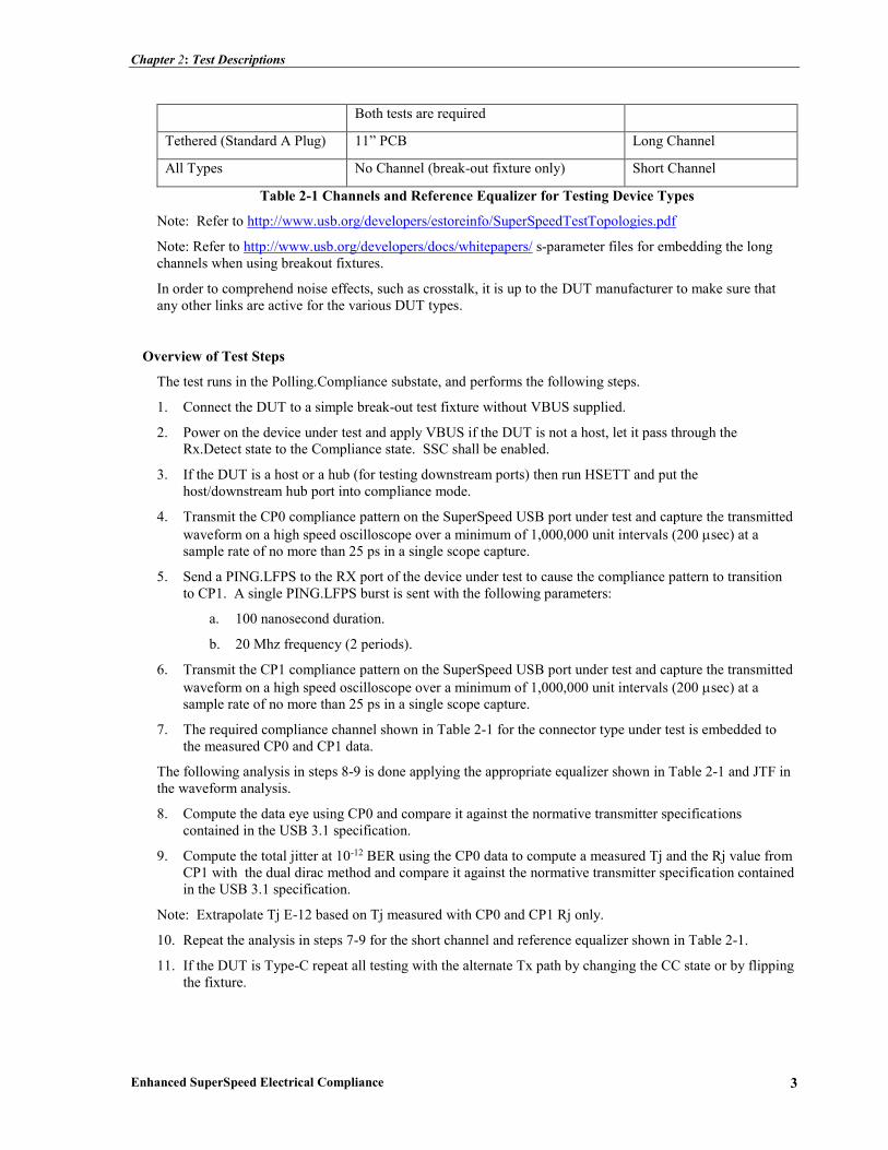
Both tests are required
Tethered (Standard A Plug) 11” PCB Long Channel
All Types No Channel (break-out fixture only) Short Channel
Table 2-1 Channels and Reference Equalizer for Testing Device Types
Note: Refer to http://www.usb.org/developers/estoreinfo/SuperSpeedTestTopologies.pdf
Note: Refer to http://www.usb.org/developers/docs/whitepapers/ s-parameter files for embedding the long
channels when using breakout fixtures.
In order to comprehend noise effects, such as crosstalk, it is up to the DUT manufacturer to make sure that
any other links are active for the various DUT types.
Overview of Test Steps
The test runs in the Polling.Compliance substate, and performs the following steps.
1. Connect the DUT to a simple break-out test fixture without VBUS supplied.
2. Power on the device under test and apply VBUS if the DUT is not a host, let it pass through the
Rx.Detect state to the Compliance state. SSC shall be enabled.
3. If the DUT is a host or a hub (for testing downstream ports) then run HSETT and put the
host/downstream hub port into compliance mode.
4. Transmit the CP0 compliance pattern on the SuperSpeed USB port under test and capture the transmitted
waveform on a high speed oscilloscope over a minimum of 1,000,000 unit intervals (200 sec) at a
sample rate of no more than 25 ps in a single scope capture.
5. Send a PING.LFPS to the RX port of the device under test to cause the compliance pattern to transition
to CP1. A single PING.LFPS burst is sent with the following parameters:
a. 100 nanosecond duration.
b. 20 Mhz frequency (2 periods).
6. Transmit the CP1 compliance pattern on the SuperSpeed USB port under test and capture the transmitted
waveform on a high speed oscilloscope over a minimum of 1,000,000 unit intervals (200 sec) at a
sample rate of no more than 25 ps in a single scope capture.
7. The required compliance channel shown in Table 2-1 for the connector type under test is embedded to
the measured CP0 and CP1 data.
The following analysis in steps 8-9 is done applying the appropriate equalizer shown in Table 2-1 and JTF in
the waveform analysis.
8. Compute the data eye using CP0 and compare it against the normative transmitter specifications
contained in the USB 3.1 specification.
9. Compute the total jitter at 10-12 BER using the CP0 data to compute a measured Tj and the Rj value from
CP1 with the dual dirac method and compare it against the normative transmitter specification contained
in the USB 3.1 specification.
Note: Extrapolate Tj E-12 based on Tj measured with CP0 and CP1 Rj only.
10. Repeat the analysis in steps 7-9 for the short channel and reference equalizer shown in Table 2-1.
11. If the DUT is Type-C repeat all testing with the alternate Tx path by changing the CC state or by flipping
the fixture.

Chapter 2: Test Descriptions
Enhanced SuperSpeed Electrical Compliance 4
TD.1.4 Transmitted Eye Test at 10 GT/s
This test verifies that the transmitter meets the eye width, eye height, deterministic jitter and random jitter
requirements when measured at the compliance test port with nominal transmitter equalization and after
processing with the appropriate channels and post processing as shown in Table 2-2.
Connector Type Channel Reference Equalizer
Std-A Device Under Test >> USB 3.1 Host Fixture 1A >>
SCOPE (Embed 6dB Cable + Device PCB)
SSGen2_TxComp12p2dB_Embedding.s4p
Long Channel
Micro-B Device Under Test >> USB 3.1 Device Fixture 1A
>> SCOPE (Embed 6dB Cable + Host PCB)
SSGen2_TxComp12p2dB_Embedding.s4p
Long Channel
Micro-AB (Host
Only)
Device Under Test >> USB 3.1 Device Fixture 1A
>> SCOPE (Embed 6dB Cable + Device PCB)
SSGen2_TxComp12p2dB_Embedding.s4p
Long Channel
Micro-AB (DRD) Device Under Test >> USB 3.1 Device Fixture 1A
>> SCOPE (Embed 6dB Cable + Host/Device PCB)
SSGen2_TxComp12p2dB_Embedding.s4p
Long Channel
Type-C (Host) Device Under Test >> USB 3.1 Host Fixture 1C >>
SCOPE (Embed 6dB Cable + Host/Device PCB)
SSGen2_TxComp12p2dB_Embedding.s4p
Long Channel
Type-C (Device) Device Under Test >> USB 3.1 Device Fixture 1C
>> SCOPE (Embed 6dB Cable + Host/Device PCB)
SSGen2_TxComp12p2dB_Embedding.s4p
Long Channel
Captive (Standard A
Plug)
Device Under Test >> USB 3.1 Captive Cable
Device Fixture Type-A >> SCOPE (Embed Host
PCB)
Mock_Host_Cascaded_Model_TypeC_rspl.s4p
Long Channel
Captive (Standard C
Plug)
Device Under Test >> USB 3.1 Captive Device
Fixture Type-C >> SCOPE (Embed Host PCB)
Mock_Host_Cascaded_Model_TypeC_rspl.s4p
Long Channel
All Types No Channel (breakout fixture only) Short Channel
Table 2-2 Channels and Reference Equalizer for Testing Device Types

Chapter 2: Test Descriptions
Enhanced SuperSpeed Electrical Compliance 5
Note: Refer to http://www.usb.org/developers/estoreinfo/USB3p1_Fixture_Topologies.pdf
Note: Refer to http://www.usb.org/developers/docs/whitepapers/ s-parameter files for embedding the long
channels when using breakout fixtures.
In order to comprehend noise effects, such as crosstalk, it is up to the DUT manufacturer to make sure that any
other links are active for the various DUT types.
Overview of Test Steps
The test runs in the Polling.Compliance substate, and performs the following steps.
1. Connect the DUT to a simple break-out test fixture without VBUS supplied.
2. Power on the device under test and apply VBUS if the DUT is a device, let it pass through the Rx.Detect
state to the Compliance state. SSC shall be enabled.
3. If the DUT is a host or a hub (for testing downstream ports) then run HSETT and put the
host/downstream hub port into compliance mode.
4. Send multiple PING.LFPS to the RX port of the device under test to cause the compliance pattern to
transition to CP9. PING.LFPS bursts are sent with the following parameters:
a. 100 nanosecond duration.
b. 20 Mhz frequency (2 periods).
5. Transmit the CP9 compliance pattern on the Enhanced SuperSpeed USB port under test and capture the
transmitted waveform on a high speed oscilloscope over a minimum of 2,000,000 unit intervals (200
sec) at a sample rate of no more than 12.5 ps (no interpolation is used) in a single scope capture.
6. Send a PING.LFPS to the RX port of the device under test to cause the compliance pattern to transition
to CP10. A single PING.LFPS burst is sent with the following parameters:
a. 100 nanosecond duration.
b. 20 Mhz frequency (2 periods).
7. Transmit the CP10 compliance pattern on the SuperSpeed USB port under test and capture the
transmitted waveform on a high speed oscilloscope over a minimum of 2,000,000 unit intervals (200
sec) at a sample rate of no more than 12.5 ps in a single scope capture.
8. Compute Rj using the CP10 data and compare it against the normative transmitter specifications
contained in the USB 3.1 specification (the equalizer is not applied for this step).
9. The required compliance channel shown in Table 2-2 for the connector type under test is embedded to
the measured CP9 data. No embedding is done for the short channel case.
The following analysis is done applying the reference equalizer and JTF in the waveform analysis.
10. Compute the data eye using CP9 using Rj as input from the CP10 waveform and compare it against
requirements for a 70 mV eye height and a 48.0 ps eye width both at 10-6 BER.
11. Repeat the analysis in steps 9-10 for the short channel shown in Table 2-2.
12. If the DUT is Type-C repeat all testing with the alternate Tx path by changing the CC state or by flipping
the fixture.
TD.1.5 Transmit Equalization Test at 10 GT/s
This test verifies that the transmitter meets requirements for transmit equalization.
In order to comprehend noise effects, such as crosstalk, it is up to the DUT manufacturer to make sure that
any other links are active for the various DUT types.

Chapter 2: Test Descriptions
Enhanced SuperSpeed Electrical Compliance 6
Note: A PCI Express host adaptor is tested in a system that provides a 100 Mhz PCI Express reference clock
with a valid SSC profile.
Overview of Test Steps
The test runs in the Polling.Compliance substate, and performs the following steps.
1. Connect the DUT to a break-out test fixture.
2. Power on the device under test, let it pass through the Rx.Detect state to the Polling.Compliance substate.
Note: Compliance mode may need to be enabled with a separate utility for downstream ports (host
controllers and hubs).
3. For Type-C this test is only performed for one TX differential pair position (either pair).
4. Send a PING.LFPS to the RX port of the device under test to cause the compliance pattern to transition
to CP13.
5. Transmit the CP13 compliance pattern on the USB port under test and capture the transmitted waveform
on a high speed oscilloscope over a minimum of 2,000,000 unit intervals (200 usec) at a sample interval
of no more than 12.5 ps in a single scope capture.
6. Repeat steps 4 and 5 to capture transmitted waveforms for the CP14 and CP15 compliance patterns.
7. Use the SigTest Transmitter Equalization test option to read the saved waveform files for CP13, CP14,
and CP15 and compute the transmitter equalization values from these. All transmitter equalization
values must be within their specified limits.
TD.1.6 Transmitted SSC Profile Test at 5 GT/s
This test verifies that the transmitter meets SSC profile requirements when measured at the compliance test
port with spec required TX equalization.
In order to comprehend noise effects, such as crosstalk, it is up to the DUT manufacturer to make sure that
any other links are active for the various DUT types.
Note: A PCI Express host adaptor is tested in a system that provides a 100 Mhz PCI Express reference clock
with a valid SSC profile and in a system with a 100 Mhz PCI Express reference clock that does not have SSC.
The host adaptor must pass all tests in both cases.
No transmitter testing is done with multiple downstream ports active on hosts/hubs.
Overview of Test Steps
The test runs in the Polling.Compliance substate, and performs the following steps.
8. Connect the DUT to a break-out test fixture.
9. Power on the device under test, let it pass through the Rx.Detect state to the Polling.Compliance substate.
Note: Compliance mode may need to be enabled with a separate utility for downstream ports (host
controllers and hubs).
10. For Type-C this only is tested for one TX differential pair position (either pair).
11. Send a PING.LFPS to the RX port of the device under test to cause the compliance pattern to transition
to CP1.
12. Transmit the CP1 compliance pattern on the SuperSpeed USB port under test and capture the transmitted
waveform on a high speed oscilloscope over a minimum of 2,000,000 unit intervals (400 usec) at a
sample interval of no more than 25 ps in a single scope capture.
13. Compute the phase jitter for the captured waveform and apply a 60*33KHz 3 dB cutoff frequency, 40
dB/decade Low Pass Filter to the phase jitter.

Chapter 2: Test Descriptions
Enhanced SuperSpeed Electrical Compliance 7
14. Use the filtered phase jitter to check that the SSC fundamental frequency is between 30 and 33 KHz.
15. Take the derivative of the filtered phase jitter and convert to ppm.
16. Check that twice maximum difference between points that are 0.5 uS apart in the derivative of the
filtered phase jitter is less than 1250 ppm.
17. The derivative of the filtered phase jitter is used to test that tSSC-FREQ-DEVIATION meets the USB 3.1
specification for each SSC cycle. tSSC-FREQ-DEVIATION must vary between one of the following two ranges
for each SSC cyle:
a. +300/-300 and -3700/-5300 PPM
b. -1700/-2300 and -3700/-5300 PPM
TD.1.7 Transmitted SSC Profile Test at 10 GT/s
This test verifies that the transmitter meets SSC profile requirements when measured at the compliance test
port with spec required TX equalization.
In order to comprehend noise effects, such as crosstalk, it is up to the DUT manufacturer to make sure that
any other links are active for the various DUT types.
Note: A PCI Express host adaptor is tested in a system that provides a 100 Mhz PCI Express reference clock
with a valid SSC profile and in a system with a 100 Mhz PCI Express reference clock that does not have SSC.
The host adaptor must pass all tests in both cases.
No transmitter testing is done with multiple downstream ports active on hosts/hubs.
Overview of Test Steps
The test runs in the Polling.Compliance substate, and performs the following steps.
1. Connect the DUT to a break-out test fixture.
2. Power on the device under test, let it pass through the Rx.Detect state to the Polling.Compliance substate.
Note: Compliance mode may need to be enabled with a separate utility for downstream ports (host
controllers and hubs).
3. For Type-C this only is tested for one TX differential pair position (either pair).
4. Send a PING.LFPS to the RX port of the device under test to cause the compliance pattern to transition
to CP10.
5. Transmit the CP10 compliance pattern on the SuperSpeed USB port under test and capture the
transmitted waveform on a high speed oscilloscope over a minimum of 2,000,000 unit intervals (200
usec) at a sample interval of no more than 12.5 ps in a single scope capture.
6. Compute the phase jitter for the captured waveform and apply a 60*33KHz 3 dB cutoff frequency, 40
dB/decade Low Pass Filter to the phase jitter.
7. Use the filtered phase jitter to check that the SSC fundamental frequency is between 30 and 33 KHz.
8. Take the derivative of the filtered phase jitter and convert to ppm.
9. Check that twice maximum difference between points that are 0.5 uS apart in the derivative of the
filtered phase jitter is less than 1250 ppm.
10. The derivative of the filtered phase jitter is used to test that tSSC-FREQ-DEVIATION meets the USB 3.1
specification for each SSC cycle. tSSC-FREQ-DEVIATION must vary between one of the following two ranges
for each SSC cyle:
a. +300/-300 and -3700/-5300 PPM
b. -1700/-2300 and -3700/-5300 PPM

Chapter 2: Test Descriptions
Enhanced SuperSpeed Electrical Compliance 8
TD.1.8 Receiver Jitter Tolerance Test at 5 GT/s
This test verifies that the receiver properly functions in the presence of deterministic and random jitter at
multiple frequencies. The jitter characteristics are defined by the USB 3.1 specification. In order to reduce
test time, the receiver is tested to a bit error ratio (BER) of 10-10. In order to comprehend noise effects, such
as crosstalk, it is up to the component manufacturer to make sure that any other links are active for the DUT.
The receiver test is performed with asynchronous SSC clocks in the test system and the device under test.
The test system SSC shall be triangular at the maximum specified SSC frequency (33 Khz) and downspread
5000 ppm. The test system SSC shall meet the specification limits on slew rate.
Note: When the DUT is in loopback for this test it shall not exit loopback unless it receives a warm reset or
an LFPS Exit Handshake.
Note: The test procedures for channels involving a 1 meter Micro-A to Micro-B cable assume the cable is
selected to have a well-controlled nominal loss of 3.5 DB at 2.5 GHz.
Connector Type Calibration Channel
(Using breakout fixture to
measure at end of channel)
Test Channel
Std-A 3m Cable + 5” PCB 3m Cable + 5” PCB
Std-B 3m Cable + 11” PCB 3m Cable + 11” PCB
Micro-B 3m Cable + 11” PCB 1m Cable + 11” PCB
Micro-AB (Host Only) 3m Cable + 5” PCB 1m Cable + 5” PCB +
Micro-A to Std-A
Receptacle adapter
Micro-AB (DRD) 3m Cable + 11” PCB 1m Cable + 11” PCB
(device mode)
1m Cable + 5” PCB +
Micro-A to Std-A
Receptacle adapter (host
mode)
Both tests are required
Tethered (Standard A Plug) 3m Cable + 11” PCB 8” (short) Std-A to Std-B
cable + 11” PCB
All Connector Types Must
Also Perform Short Channel
Test
Same as above (Either 3m
Cable + 5” PCB or 3m Cable
+ 11” PCB) depending on
connector type
Breakout Fixture Only
Table 2-3 Channels for Testing Device Types
Note: Refer to http://www.usb.org/developers/estoreinfo/SuperSpeedTestTopologies.pdf
Overview of Test Steps
The test runs in the Polling.Loopback substate, and performs the following steps.
1. Calibrate swing and de-emphasis

Chapter 2: Test Descriptions
Enhanced SuperSpeed Electrical Compliance 9
a. Connect the end of the cables that will connect to the SMAs on the test fixture (as directly as
possible) to a real time oscilloscope and the other end to the test equipment generator.
b. Have the test equipment transmit a pattern with 64 ones followed by 64 zeros followed by 128
bits of a 1010 clock pattern at 5 GT/s.
c. Calibrate the differential amplitude of the measured signal to 800 mV peak to peak.
d. Calibrate the measured de-emphasis to 3.0 + 0.3/-0 dB fixed de-emphasis.
Note: The signal source must support full bit de-emphasis.
2. Connect the calibration channel to the signal source.
Calibrate Rj (2.42 +/- 10% ps RMS/30.8 +/- 10% ps peak to peak at a BER of 10-10) with clock pattern (CP1).
Calibrate at the end of the channel applying the CTLE and JTF. SSC and all other noise sources are off for
this step.
Calibrate Sj (40.0 ps +0/-10% at 50 MHz) with CP0. Calibrate at the end of the channel applying only CTLE.
SSC is off for this step. (Calibration is done by testing measured maximum peak to peak jitter without
extrapolation (measured TJ) without Sj and then adding Sj until measured maximum peak to peak jitter
without extrapolation (measured Tj) increased by 40 ps). All other noise sources are off during this
calibration. A 49 KHz critically damped high pass filter with 40 dB/decade roll-off is used during Sj
calibration instead of the standard JTF.
Measure eye height with CP0 at a BER of 10-6 at the end of the channel with the host fixtures with all jitter
sources and SSC on applying the JTF and the Long channel reference CTLE. Adjust the signal source
amplitude to provide
180 mV +5/-0 mV of eye height with host test fixtures for testing a host.
145 mV +5/-0 mV of eye height with device test fixtures for testing a device.
Note: Amplitude should be calibrated to be as close to the minimum value as possible without going under
the minimum.
Note: De-emphasis at the instrument output must be adjusted to remain at 3.0 + 0.3/ - 0 dB after the eye
height calibration process is complete.
After calibration is complete the Tj at a BER of 10-12 with CP0 and all jitter sources on must be between 90
and 95 picoseconds. This measurement is done only with the Sj frequency of 50 Mhz and is performed by
checking the average Tj over three 1 million unit interval oscilloscope captures. Due to degradation in
connections in the test channel or other test channel issues it may be necessary to switch to a new test channel
to achieve a calibrated Tj value in the expected range.
3. Connect the DUT to the appropriate test channel.
4. Power on the device under test.
5. Transmit 400 Polling.LFPS (4ms).
Note that all jitter sources are added during all transmissions to the device under test. If the device does
not go into loopback it fails the test.
6. Transmit 65536 TSEQ.
7. Transmit 256-65536 TS1.
8. Transmit 256-65536 TS2 with loopback bit set.
9. Start transmitting the BDAT test pattern.
10. Transmit BDAT for 2 ms before starting error calculations.

Chapter 2: Test Descriptions
Enhanced SuperSpeed Electrical Compliance 10
11. Transmit the BDAT sequence from the signal source for a total of 3x10⁹ symbols (3x1010 bits). A single
SKP ordered set is inserted in the sequence every 354 symbols.
12. The DUT fails if more than one error is encountered. .
Note: The channel to the test equipment receiver is kept as short and clean as possible.
13. Repeat steps 3-11 with 40.0 +0/-10% ps of periodic (sinusoidal) at a 33 MHz frequency with -3dB of
equalization.
14. Repeat steps 3-11 with 40.0 +0/-10% ps of periodic (sinusoidal) at a 20 MHz frequency with -3dB of
equalization.
15. Repeat steps 3-11with 40.0 +0/-10% ps of periodic (sinusoidal) at a 10 MHz frequency with -3dB of
equalization.
16. Repeat steps 3-11 with 40.0 +0/-10% ps of periodic (sinusoidal) at a 4.9 MHz frequency with -3dB of
equalization.
17. Repeat steps 3-11 with 100 +0/-5% ps of periodic (sinusoidal) at a 2 MHz frequency with -3dB of
equalization.
18. Repeat steps 3-11 with 200 +0/-5% ps of periodic (sinusoidal) at a 1 MHz frequency -3dB of
equalization.
19. Repeat steps 3-11 with 400 +0/-5% ps of periodic (sinusoidal) at a 500 KHz frequency -3dB of
equalization.
Connect scope directly to the signal source with the signal source keeping all settings the same as the calibrated
settings with the calibration channel.
20. Measure the maximum peak to peak differential voltage with a pattern with 64 ones followed by 64 zeros
followed by 128 bits of a 1010 clock pattern at 5 GT/s with all jitter sources, Tx Equalization, and SSC
off. Adjust amplitude to provide a maximum peak to peak differential voltage of 1200 mV +0/-20 mV
using the clock portion of the pattern for the measurement.
21. Turn all jitter sources, Tx Equalization and SSC on to the same settings as the long channel calibration
and complete the short channel test with the DUT connected directly to the breakout fixture.
Note: Amplitude should be calibrated to be as close to the maximum value as possible without going over the
maximum.
Note: De-emphasis at the instrument output must be adjusted to remain at 3.0 + 0.3/ - 0 dB.
22. Repeat steps 3-19.
TD.1.9 Receiver Jitter Tolerance Test at 5 GT/s (Type-C)
This test verifies that the receiver properly functions in the presence of deterministic and random jitter at
multiple frequencies. The jitter characteristics are defined by the USB 3.1 specification. In order to reduce
test time, the receiver is tested to a bit error ratio (BER) of 10-10. In order to comprehend noise effects, such
as crosstalk, it is up to the component manufacturer to make sure that any other links are active for the DUT.
The receiver test is performed with asynchronous SSC clocks in the test system and the device under test.
The test system SSC shall be triangular at the maximum specified SSC frequency (33 Khz) and downspread
5000 ppm. The test system SSC shall meet the specification limits on slew rate.
Note: When the DUT is in loopback for this test it shall not exit loopback unless it receives a warm reset or
an LFPS Exit Handshake.

Chapter 2: Test Descriptions
Enhanced SuperSpeed Electrical Compliance 11
Connector Type Calibration Channel Test Channel
Type-C (Host) All calibration at BERT
output
BERT -> 5G Host/Device
Fixture 2 (14.4”) -> 7 dB
cable -> Host Fixture 1C -
> DUT
Type-C (Device) All calibration at BERT
output
BERT -> 5G Host/Device
Fixture 2 (14.4”) -> 7 dB
cable -> Device Fixture
1C -> DUT
All Connector Types Must
Also Perform Short Channel
Test
All calibration at BERT
output
BERT-> USB 3.1 Full
Type-C Breakout -> DUT
Table 2-4 Channels for Testing Device Types
Note: Refer to http://www.usb.org/developers/estoreinfo/USB3p1_Fixture_Topologies.pdf
Overview of Test Steps
The test runs in the Polling.Loopback substate, and performs the following steps.
1. Calibrate swing and de-emphasis
a. Connect the end of the cables that will connect to the SMAs on the test fixture (as directly as
possible) to a real time oscilloscope and the other end to the test equipment generator.
b. Have the test equipment transmit a pattern with 64 ones followed by 64 zeros followed by 128
bits of a 1010 clock pattern at 5 GT/s.
c. Calibrate the differential amplitude of the measured signal to 800 mV peak to peak.
d. Calibrate the measured de-emphasis to 3.0 + 0.3/-0 dB fixed de-emphasis.
Note: The signal source must support full bit de-emphasis.
2. Calibrate Rj and Sj.
Calibrate Rj (2.42 +/- 10% ps RMS/30.8 +/- 10% ps peak to peak at a BER of 10-10) with clock pattern (CP1).
Calibrate after applying only the JTF. SSC and all other noise sources are off for this step.
Calibrate Sj (40.0 ps +0/-10% at 50 MHz) with CP0. Calibrate applying only a 49 KHz critically damped
high pass filter with 40 dB/decade roll-off instead of the standard JTF. SSC is off for this step. (Calibration
is done by testing measured maximum peak to peak jitter without extrapolation (measured TJ) without Sj and
then adding Sj until measured maximum peak to peak jitter without extrapolation (measured Tj) increased by
40 ps). All other noise sources are off during this calibration.
3. Connect the calibration channel to the signal source.
4. Connect the DUT to the appropriate test channel.
5. Power on the device under test.
6. Transmit 400 Polling.LFPS (4 ms).
Note that all jitter sources are added during all transmissions to the device under test. If the device does
not go into loopback it fails the test.
7. Transmit 65536 TSEQ.

Chapter 2: Test Descriptions
Enhanced SuperSpeed Electrical Compliance 12
8. Transmit 256-65536 TS1.
9. Transmit 256-65536 TS2 with loopback bit set.
10. Start transmitting the BDAT test pattern.
11. Transmit BDAT for 2 ms before starting error calculations.
12. Transmit the BDAT sequence from the signal source for a total of 3x10⁹ symbols (3x1010 bits). A single
SKP ordered set is inserted in the sequence every 354 symbols.
13. The DUT fails if more than one error is encountered. .
Note: The channel to the test equipment receiver is kept as short and clean as possible.
14. Repeat steps 3-13 with 40.0 +0/-10% ps of periodic (sinusoidal) at a 33 MHz frequency with -3dB of
equalization.
15. Repeat steps 3-13 with 40.0 +0/-10% ps of periodic (sinusoidal) at a 20 MHz frequency with -3dB of
equalization.
16. Repeat steps 3-13 with 40.0 +0/-10% ps of periodic (sinusoidal) at a 10 MHz frequency with -3dB of
equalization.
17. Repeat steps 3-13 with 40.0 +0/-10% ps of periodic (sinusoidal) at a 4.9 MHz frequency with -3dB of
equalization.
18. Repeat steps 3-13 with 100 +0/-5% ps of periodic (sinusoidal) at a 2 MHz frequency with -3dB of
equalization.
19. Repeat steps 3-13 with 200 +0/-5% ps of periodic (sinusoidal) at a 1 MHz frequency -3dB of
equalization.
20. Repeat steps 3-13 with 400 +0/-5% ps of periodic (sinusoidal) at a 500 KHz frequency -3dB of
equalization.
Connect the scope directly to the signal source with the signal source keeping all settings the same as the
calibrated settings with the calibration channel.
21. Measure the maximum peak to peak differential voltage with a pattern with 64 ones followed by 64 zeros
followed by 128 bits of a 1010 clock pattern at 5 GT/s with all jitter sources, Tx Equalization, and SSC
off. Adjust amplitude to provide a maximum peak to peak differential voltage of 1200 mV +0/-20 mV
using the clock portion of the pattern for the measurement.
22. Turn all jitter sources, Tx Equalization and SSC on to the same settings as the long channel calibration
and complete the short channel test with the DUT connected directly to the breakout fixture.
Note: Amplitude should be calibrated to be as close to the maximum value as possible without going over the
maximum.
Note: De-emphasis at the instrument output must be adjusted to remain at 3.0 + 0.3/ - 0 dB.
23. Repeat steps 3-19.
24. If the DUT is Type-C repeat all testing with the alternate Rx path by changing the CC state or by flipping
the fixture.
TD.1.10 Receiver Jitter Tolerance Test at 10 GT/s
This test verifies that the receiver properly functions in the presence of deterministic and random jitter at
multiple frequencies. The jitter characteristics are defined by the USB 3.1 specification. In order to

Chapter 2: Test Descriptions
Enhanced SuperSpeed Electrical Compliance 13
comprehend noise effects, such as crosstalk, it is up to the component manufacturer to make sure that any
other links are active for the DUT.
The receiver test is performed with asynchronous SSC clocks in the test system and the device under test.
The test system SSC shall be triangular at the maximum specified SSC frequency (33 Khz) and downspread
5000 ppm. The test system SSC shall meet the specification limits on slew rate.
Note: When the DUT is in loopback for this test it shall not exit loopback unless it receives a warm reset or
an LFPS Exit Handshake.
Note: The test procedures for channels involving a USB cable assume the cable is selected to have a well-
controlled nominal loss of 6.0 dB at 5.0 GHz.
Connector Type Calibration Channel
(Using breakout fixture to
measure at end of channel)
Test Channel
Std-A BERT >> USB 3.1
Compliance Load Board >>
6 dB Cable >> USB 3.1
Host Fixture 1A >> USB
3.1 Mock Host 7.2” >>
SCOPE
BERT >> USB 3.1
Compliance Load Board
>> 6 dB Cable >> USB
3.1 Host Fixture 1A >>
Host Under Test
Micro-B BERT >> USB 3.1
Compliance Load Board >>
6 dB Cable >> USB 3.1
Device Fixture 1A >> USB
3.1 Mock Device 7.2” >>
SCOPE
BERT >> USB 3.1
Compliance Load Board
>> 6 dB Cable >> USB
3.1 Device Fixture 1A >>
Device Under Test
Micro-AB (Host Only) BERT >> USB 3.1
Compliance Load Board >>
6 dB Cable >> USB 3.1
Device Fixture 1A >> USB
3.1 Mock Device 7.2” >>
SCOPE
BERT >> USB 3.1
Compliance Load Board
>> 6 dB Cable >> USB
3.1 Device Fixture 1A >>
Device Under Test
Micro-AB (DRD) BERT >> USB 3.1
Compliance Load Board >>
6 dB Cable >> USB 3.1
Device Fixture 1A >> USB
3.1 Mock Device 7.2” >>
SCOPE
BERT >> USB 3.1
Compliance Load Board
>> 6 dB Cable >> USB
3.1 Device Fixture 1A >>
Device Under Test
Captive (Standard A Plug) BERT >> USB 3.1
Compliance Load Board >>
6 dB Cable >> USB 3.1
Device Fixture 1A >> USB
3.1 Mock Device 7.2” >>
SCOPE
BERT >> USB 3.1
Captive Cable Device
Fixture Type-A >> Device
Under Test
Type-C Host BERT >> USB 3.1
Compliance Load Board
Type–C >> 6 dB Cable >>
USB 3.1 Host Fixture 1C
>> USB 3.1 Mock
BERT >> USB 3.1
Compliance Load Board
Type–C >> 6 dB Cable >>

Chapter 2: Test Descriptions
Enhanced SuperSpeed Electrical Compliance 14
Host/Device Type-C 7.2” >>
SCOPE
USB 3.1 Host Fixture 1C
>> Device Under Test
Type-C Device BERT >> USB 3.1
Compliance Load Board
Type–C >> 6 dB Cable >>
USB 3.1 Device Fixture 1C
>> USB 3.1 Mock
Host/Device Type-C 7.2” >>
SCOPE
BERT >> USB 3.1
Compliance Load Board
Type–C >> 6 dB Cable >>
USB 3.1 Device Fixture
1C >> Device Under Test
Captive (Type-C Plug) BERT >> USB 3.1
Compliance Load Board
Type–C >> 6 dB Cable >>
USB 3.1 Device Fixture 1C
>> USB 3.1 Mock
Host/Device Type-C 7.2” >>
SCOPE
BERT >> USB 3.1
Captive Device Fixture
Type-C >> Device Under
Test
All Connector Types Must
Also Perform Short Channel
Test
See procedure for short
channel calibration details
For Type –C
BERT>>USB 3.1 Full
Type-C Breakout>>DUT
For Standard A – Use
breakout fixture from a
test vendor used for 5
GT/s testing
Table 2-5 Channels for Testing Device Types
Note: Refer to http://www.usb.org/developers/estoreinfo/USB3p1_Fixture_Topologies.pdf
Note: All cable losses in dB are at 5 GHz
Overview of Test Steps
The test runs in the Polling.Loopback substate, and performs the following steps.
1. Calibrate swing and de-emphasis without the test channel.
a. Connect the end of the SMA cables that will connect to the SMAs on the test fixture (as
directly as possible) to a real time oscilloscope and the other end to the test equipment
generator.
b. Have the test equipment transmit a pattern with 64 ones followed by 64 zeros followed by 128
bits of a 1010 clock pattern at 10 GT/s.
c. Measure the transmitted signal on the oscilloscope and adjust the post cursor de-emphasis and
swing of the generator until the low frequency and high frequency portions of the signal have
an equal differential amplitude of 800 mV peak to peak..
d. Calibrate the measured TX EQ to 2.2 +/- .1 dB fixed preshoot
e. Calibrate the TX EQ de-emphasis settings for -1.0 +/- .1 dB, -3.1 +/- 1 dB, and -5.0 +/- .1 dB
Note: The signal source must support full bit de-emphasis.

Chapter 2: Test Descriptions
Enhanced SuperSpeed Electrical Compliance 15
2. Calibrate Rj (1.0 +0/-.1 ps RMS) with clock pattern (CP10). Calibrate after applying the JTF. The
reference equalizer is not used for this Rj calibration. SSC is off and all other jitter sources are on but set
to zero.
3. Calibrate Sj (17.0 ps +0/-10% at 100 MHz) with CP9. Calibrate without reference receiver equalization.
SSC is off and all other jitter sources are on but set to zero. Calibration is done by testing measured
maximum peak to peak jitter without extrapolation (measured TJ) without Sj and then adding Sj until
measured maximum peak to peak jitter without extrapolation (measured Tj) increased by 17 ps. A 75
KHz critically damped high pass filter with 40 dB/decade roll-off is used during Sj calibration instead of
the standard JTF.
4. Connect the calibration channel to the signal source using the shortest compliance load board (5.6”).
5. Measure eye height with CP9 at a BER E-6 using the calibrated Sj and Rj values with SSC enabled. The
eye height is measured after applying the JTF, the reference CTLE curve fixed to a DC gain of -5 dB,
and DFE.
6. Change the compliance load board to the mid-length (7.1”) and repeat the eye height measurement.
7. Change the compliance load board to the longest (8.1”) and repeat the eye height measurement.
8. Select the compliance load board that yields the eye height measurement closest to 70 mV and use this
compliance load board for the remaining calibration and testing.
9. Adjust the de-emphasis from 1 dB to 5 dB to adjust the eye width with a target of 48 +2/-0 ps. The width
is measured after applying JTF, the reference equalizer CTLE curve fixed to a DC gain of -5 dB, and
DFE. SSC is still enabled for this step.
10. If the width target was not met in step 10 then:
a. If the width is too big then add a second Sj tone at 87 MHz and adjust until the width target is
met.
b. If the width is too small then reduce the 100 MHz Sj tone until the width target is met.
Note: If the adjustment in step 10a or 10b is bigger than 5 ps then there is likely a problem with the fixtures or
set-up.
11. Adjust the signal source amplitude to provide
70 mV +5/-0 mV of eye height with calibration channel.
Note: Amplitude should be calibrated to be as close to the minimum value as possible without going under
the minimum.
12. Connect the DUT to the appropriate test channel.
13. Power on the device under test.
Note: If the BERT is protocol aware it is allowed to just follow the protocol rules in the base specification
14. BERT sends following sequences
a. 2-32 SCD1
b. 2-32 SCD2
c. 4-32 LBPM (w PHY capability).
d. 4-32 LBPM (w PHY ready)
Note that all jitter sources are added during all transmissions to the device under test. If the device does
not go into loopback it fails the test.
15. Transmit 524,288 - 577,288 TSEQ It is preferred for the BERT to transmit as close to 524,288 TSEQ as
possible. If a device requires a number of TSEQ outside this range to pass the test this is a failure.
16. Transmit 31 - 65536 TS1. (SYNC, 31 TS1, SKP – repeat to up to 65536 total TS1)
17. Transmit 31 - 65536 TS2 with loopback bit set.

Chapter 2: Test Descriptions
Enhanced SuperSpeed Electrical Compliance 16
18. Start transmitting the CP9 test pattern.
19. Transmit CP9 for 2 ms before starting error calculations.
20. Transmit a “modified” CP9 sequence from the signal source for a total of 2 minutes. The modified CP9
pattern starts with a SYNC ordered set. Then data blocks are added and scrambled with the USB10G
specific PRBS-23 scrambler polynomial. A single SKP ordered set with 20SKP symbols (192 bits) must
be inserted in the sequence every 40 blocks. At least 65536 data blocks must be sent before the pattern is
repeated.
21. The DUT fails if more than one error is encountered. .
Note: The channel to the test equipment receiver is kept as short and clean as possible.
Note: if adjustments were made in step 10 they are kept for each additional Sj frequency. If an 87
MHz tone was used it is kept at the same magnitude for each Sj frequency. If the 100 MHz Sj tone
was reduced the Sj targets at each other frequency are reduced by the same amount in ps.
22. Repeat steps 14-21 with 17.0 +0/-10% ps of periodic (sinusoidal) at a 50 MHz frequency.
23. Repeat steps 14-21 with 17.0 +0/-10% ps of periodic (sinusoidal) at a 30 MHz frequency.
24. Repeat steps 14-21 with 17.0 +0/-10% ps of periodic (sinusoidal) at a 15 MHz frequency.
25. Repeat steps 14-21 with 17.0 +0/-10% ps of periodic (sinusoidal) at a 7.5 MHz frequency.
26. Repeat steps 14-21 with 37.0 +0/-5% ps of periodic (sinusoidal) at a 4 MHz frequency.
27. Repeat steps 14-21 with 87.0 +0/-5% ps of periodic (sinusoidal) at a 2 MHz frequency.
28. Repeat steps 14-21 with 203.0 +0/-5% ps of periodic (sinusoidal) at a 1 MHz frequency.
29. Repeat steps 14-21 with 476.0 +0/-5% ps of periodic (sinusoidal) at a 500 KHz frequency.
Connect the scope directly to the signal source with the signal source keeping all settings the same as the
calibrated settings with the calibration channel.
30. Measure the maximum peak to peak differential voltage with a pattern with 64 ones followed by 64 zeros
followed by 128 bits of a 1010 clock pattern at 10 GT/s with all jitter sources, Tx Equalization, and SSC
off. Adjust amplitude to provide a maximum peak to peak differential voltage of 1200 mV +0/-20 mV
using the clock portion of the pattern for the measurement.
Note: Amplitude should be calibrated to be as close to the maximum value as possible without going over the
maximum. TX EQ must not change during this calibration.
31. Turn all jitter sources, Tx Equalization, and SSC on to the same settings as the long channel calibration
and complete the short channel test with the DUT connected directly to the breakout fixture.
32. Repeat steps 12-29
33. If the DUT is Type-C repeat all testing with the alternate Rx path by changing the CC state or by flipping
the fixture. If the CC state is changed the eye calibration is repeated for the new fixture path.