electrical phenomena in amorphous oxide films -...
TRANSCRIPT

Electrical phenomena in amorphous oxide films
G. DEARNALEY,? A. M. STONEHAM,? AND D. V. MORGANS t AERE, Harwell, Didcot, Berks. $ Department of Electrical and Electronic Engineering, University of Leeds
Contents
1. Introduction . 1.1. Charge transport in insulators . 1.2. Differential negative resistance . 1.3. Dielectric breakdown . 2.1. Observations of forming . 2.2. Models of the forming process
3.1. Observations of conduction, switching and memory phenomena 3.2. Theories of switching and memory in oxide films . 3.3. Observations on triodes .
. 4.1. Electron emission . 4.2. Electroluminescence in M-I-M (metal-insulator-metal) struc-
4.3, Theories of electron emission and electroluminescence . 4.4. Injection electroluminescence in MOS (metal-oxide-semi-
4.5. Noise . 5.1, Current-controlled negative resistance and bistable switching
5.2. Comparison with the Ovshinsky devices 5.3. A comparison of switching in crystalline, microcrystalline and
2. The forming process . .
3. Conduction, switching and memory phenomena .
4. Electron emission, luminescence and other phenomena
tures .
conductor) structures . . 5. Comparison with other systems
in oxides. .
amorphous films . 6. Practical implications .
6.1. Switches . 6.2. Memory arrays . 6.3. Hot electron, cold cathode emitter 6.4. Alpha-numeric display panel . 6.5. Electroluminescent MOS devices . 6.6. Oxide-coated cathodes . 6.7. MOS capacitors and transistors . 6.8. Surface barrier diodes . 6.9. Anodic oxides and corrosion .
6.10. Anodic electret microphones .
.
7. Conclusions. References .
Page 1130 1131 1134 1137 1138 1138 1142 1146 1146 1151 1162 1163 1164
1165 1168
1169 1171 1172
1172 1176
1178 1179 1179 1180 1181 1181 1182 1182 1183 1184 1186 1187 1187 1188
Abstract. Thin layers of insulators, from 100 A to 20 000 A thick, have a number of interesting electrical properties. These properties include forming, which is a profound and essentially permanent change produced by an electrical field, and, after forming, differential negative resistance together with switching and memory phenomena. Electroluminescence and electron emission also occur.
These features are shown by most amorphous or microcrystalline insulators of the appropriate thickness, and are particularly clearly shown by the oxides, such as
Rep. Prog. Phys., 1970, 33, 1129-1191
1130 G. Dearnaley, A. M. Stoneham and D. V. Morgan
A1,0,, Ta,05 and SiO. In our review we survey the observed properties of metal-insulator-metal devices involving such insulating layers, and discuss the mechanisms which have been proposed for their operation. Further, since the unusual properties may be technologically important, we outline some of the possible uses of these devices and the relevance of the phenomena to the mechanism of corrosion of certain metals.
1. Introduction Thin layers of insulators, between about 100 A and 2 pm in thickness, frequently
possess rather unusual electrical properties. Some of these were at first dismissed as due to ‘breakdown’ of an unspecified nature, ‘pinholes’ through the film, and so on. I t is now recognized that the effects fall into a more definable category and that they are not electrical breakdown in the strict sense. These properties include the phenomena of ‘forming’, which is a profound and essentially irreversible change in conductivity induced by a high electric field. After forming, differential negative resistance together with switching and memory phenomena are observed. Further- more, in suitable structures, electroluminescence and electron emission may occur.
These properties are displayed by a rather wide range of amorphous or micro- crystalline binary inorganic insulators prepared under suitable conditions in films of the appropriate thickness. They are not confined to the oxides but are particularly well demonstrated by oxides such as SiO,, Ta2O6, Nb,O,, Al,O,-hence our choice of title. Oxide films are common on metals and semiconductors and for this reason the effects have been studied more frequently in oxides than in the halides and sulphides which also sometimes show a similar behaviour. Apparently similar phenomena have been reported in films of a few more complex substances such as cryolite, polymethyl methacrylate (Lewowski et al. 1965) and polydivinylbenzene (Gregor 1966).
In this review, we shall survey the observed properties of metal-insulator-metal and metal-insulator-semiconductor structures, and discuss the varied mechanisms which have been proposed to explain their operation. We shall dwell only briefly on the properties of very thin films, below about 50 A in thickness, where it would appear that electron tunnelling processes can account satisfactorily, and in a relatively conventional manner, for the observed conductivity. Such phenomena have been discussed at length by Duke (1969). Nor shall we be much concerned with the low-field conduction, prior to forming. These low-current conduction mechanisms, while still not fully understood, appear to make only a minor con- tribution to the electrical behaviour once the field-induced behaviour has been established. Hill (1967, 1971) has given a good review of the conduction mechanisms of unformed insulators. We shall concentrate most attention on the class of struc- tures which exhibits voltage-controlled behaviour in negative resistance and switching. There is another class of devices, exemplified by the chalcogenide glass films and the so-called ‘ Ovshinsky devices’, which shows current-controlled behaviour. This class has received a great deal of attention of late, and we feel that a reasonable explanation of the switching action has now been put forward (Warren 1970). We shall try to put into perspective these two classes of behaviour, both of which are observed in oxide films, and to derive a criterion for deciding which will occur. It may well be that both classes of device share common precursor pro- cesses, before conduction fully commences, and that these are easier to observe in the oxide structures.

Electrical phenomena in amorphous oxide films 1131
Although far less publicized attention has been given to amorphous oxide devices, there has been a longer history of observation and interest in them dates back over more than ten years (Kreynina et al. 1960); Hickmott in the USA has been particularly active in the field. Moreover, the effects we shall describe are probably significant in several devices of current technological importance, as well as in novel structures which have yet to find a place alongside conventional semi- conductor device technology. They may be involved, too, in corrosion and anodic oxidation to an extent not hitherto realized. A recent report by the Science Research Council (SRC 1970) has summarized work in the UK on amorphous materials, yet it reveals exceedingly sparse interest in oxide films. It would be a pity if the glare of publicity afforded to a particular development in the field rendered us blind to other approaches, and determined the shaping of research effort for several years.
For this reason, it seems timely to adopt a broad viewpoint and to summarize for a wider readership the entangled literature on thin oxide films and the problems that remain. There is still a considerable controversy about the mechanisms involved and the degree to which the medium can be regarded as homogeneous and amenable to band theory.
Before considering these matters in detail we shall, by way of introduction, consider rather generally the current-carrying mechanisms in insulators and the nature of dielectric breakdown. After this, the forming process will be considered, and two further sections discuss the associated phenomena. A discussion of the status of the models and a comparison with Ovshinsky devices follows in $ 5 , and the device implications of the phenomena are considered in some detail in $6.
1.1. Charge transport in insulators The insulators we shall be considering will largely be noncrystalline and may
contain a significant proportion of impurities. The current may be carried by electrons or holes, or by ionic motion, We begin by considering electronic motion in such systems.
Several of these processes show a pronounced temperature dependence, since they involve thermal activation in some form. One common process is Schottky emission, or the field-assisted emission of electrons over the barrier at a metal- insulator interface. The effect is thermally activated and gives a current,
J, = AT2exp - --a-- (2 Ej where A is the effective Richardson constant, A, the barrier height and E the applied field. The process is said to be ' electrode-controlled'. Generalizations of this result are discussed by Simmons (1965) for cases where the electron mean free path is small. A related phenomenon is associated with emission over barriers which may exist within the bulk of the insulator, typically at localized trapping sites. The field-enhanced thermal excitation into the conduction band of electrons trapped by immobile positive charges is called Poole-Frenkel emission, and gives rise to a current
JPF = BEexp - --p- (2 where /3 = 201. A more exact expression is given by Jonscher (1967).

1132 G. Dearnaley, A. M . Stoneham and D. V. Morgan
Thermally activated hopping between localized electronic states may occur in impurity conduction. For hopping conduction
J H = JoEexp (-2) Here AI%, the effective activation energy, is less well defined, and it is inappropriate to think of electrons propagating with some typical mean free path. Mott (1967, 1968 a, b, c) has observed that the activation energy AH tends to zero as the tem- perature tends to zero, since the only hopping transitions which will be energetically allowe& will be those which involve traps equivalent in energy. The activation energy also tends to zero at a critical concentration of traps, when the insulator becomes a conductor. Hopping conduction always requires some degree of com- pensation (Mott 1956, Miller and Abrahams 1960); further, the ac conductivity always exceeds the dc conductivity and increases with frequency.
If the rate of carrier injection at a contact exceeds the rate of transport away from the contact, we have the bulk-limited situation described as space-charge- limited current flow (h'Iott and Gurney 1948). A general review is given by Lampert and Mark (1970). For very low injected carrier densities much less then the thermally generated carrier density, Ohm's law is obeyed. The space-charge-limited current has nonlinear dependence on the applied field
where p is the electron mobility and d the insulator thickness. The constant of proportionality depends, among other things, on the presence of traps within the insulator. At higher fields E > (8 r /e , ) No ed, where No is the carrier density at the metal-insulator interface, J ceases to be space-charge limited and varies linearly with the field at the cathode interface. The critical voltage for the change to ohmic behaviour is given by
so that the change may occur within the range of parameters we are considering. Besides the space-charge-limited current we have already considered there are
other electronic processes which do not exhibit a pronounced temperature depen- dence. I n very thin films (typically less than 100 A) tunnelling can be important (Mead 1961), but it need not concern us for the range of film thickness under discussion in this review.
There are some circumstances in which an insulator may become conducting, for example, by virtue of a phase transition, either as a whole or in localized regions. I t is clear that in these cases, the current-voltage relation can have the usual Ohm's law form once the conducting phase has become established.
Ionic conduction shows the thermally activated form :
Usually the ionic conductivity is small, since the ionic mobilities are small. If the ionic mobility (drift velocity per unit applied field) is typically cm2 s-l V-l at

Electrical phenomena in amorphous oxide $films 1133
1200 K and A, is 1 eV, then at 300 "C the mobility is only cm2 s-I V-l. In this case the mean time to cross a film of thickness 100 A under an applied field of 5 V is about half an hour, considerably longer than any of the characteristic times with which we shall be concerned. However, we cannot rule out the possibility of rapid diffusion which results from the amorphous or microcrystalline nature of the insulator. In such cases the mobility should be sensitive to the detailed mode of preparation of the specimen.
In deciding the mechanism of charge transport, difficulties arise similar to those which occur in discussions of tunnelling (Duke 1969). Theoretically, it is customary to use a phenomenological approach. This uses one-electron theory, often in the form of the effective-mass approximation and a simple model of the band structure. The one-electron potential contains image-force terms in the insulator and a Tvacuum Insulator
Work func t ion Conduction
I Banr Figure 1. A schematic representation of the band structure of a metal and an insulator. The
vacuum levels of the bulk components are equated at the interface so that the results are expressed in terms of the metal work functions and the insulator electron affinities.
contribution, calculated from Poisson's equation, to allow for local deviations from charge neutrality. It is difficult in practice to distinguish between surface charges and bulk space-charge terms, so further assumptions are necessary. Further, fluctuations in the position, potential energy discontinuity and electric field at the interfaces are ignored. The neglect of fluctuations may lead to qualitative errors, and possibly to a misunderstanding of effects which arise, in part, from such fluctuations. Dielectric breakdown, for instance, is affected by the details of the interface (Alpert et al. 1964). The relative positions of band structures in adjacent components are treated as adjustable parameters. At best, these are fixed by independent experiment. However, it is more common to equate vacuum levels of the bulk components, so that the results are expressed in terms of metal work functions and insulator electron affinities (figure 1). In general, this equation is not accurate, since the discontinuity at the interface can disturb the local electronic structure of the components considerably. Moreover, even nominally 'symmetric' devices may not have symmetric properties if the method of preparation differed for the two metal-insulator faces. This asymmetry is usually associated with the kinetics of oxide growth (Smith and Miles 1963, Fromhold and Cook 1967 a, b). It is only possible to assume general trends of behaviour with work function and electron affinity. Experimentally, one must ask how a particular mechanism may be verified, whether the dependence on fabrication (if any) is consistent and, in par- ticular, whether the interpretation is unique. The mechanism of carrier transport in the thin films under discussion has not been conclusively identified, and the several interpretations are very different.
44

1134 G. Dearnaley, A. M . Stoneham and D. V . Morgan
1.2. Differential negative resistance Systems which show differential negative resistance are divided into two classes :
the current-controlled (S-type) and the voltage-controlled (N-type) types. The current-voltage characteristics are shown in figure 2. The thin-film devices we shall primarily be concerned with have an N-type characteristic.
The mechanisms which give rise to differential negative resistance fall into three broad categories : (i) processes in which the Joule heating of the conduction electrons causes a change in their number or in their mobility, (ii) processes in which special semi-permanent space-charge distributions are set up, and (iii) processes which involve a phase change or atomic rearrangement of the host insulator. A number of these processes are reviewed by Volkov and Kogan (1969).
Voltage ( V 1 Voltage ( V I
Figure 2. Two types of differential negative resistance: (a) voltage controlled (b) current controlled
The most commonly considered mechanisms are those in the first category. One example is the superheating mechanism. Certain scattering processes, such as electron collisions with charged ions or electron interactions with piezoelectric phonons, become less efficient at high electron energies. The electron mobility can then rise suddenly, giving an S-type characteristic, once enough of the electrons have sufficient energy. A second example is the Gunn effect. I n certain semi- conductors, such as GaAs and InP, the conduction band has a minimum at K = 0 together with higher-energy minima with larger effective masses. As the electrons are heated they populate the higher minima, lowering their mobility ( p cc m*-l) and giving an N-type characteristic. In a third example, also giving an N-type characteristic, higher-energy electrons are more easily captured by trapping centre, so that their mobility is reduced. Thus Au2- in Ge can trap an electron, but because of the long-range repulsive field, such trapping is only possible for electrons of higher energy. A fourth process can occur in compensated semiconductors. Impact ionization can increase the number of carriers; this, combined with the decrease of scattering at higher electron energies, gives rise to an S-type characteristic.
The second category, in which a special space-charge distribution is set up and which gives rise to the differential negative resistance, includes three models of particular relevance. These are the models of Hickmott (1962, 1964 a, b, 19’70 private communication), of Simmons and Verderber (1967 a) for oxide films and of Mott (1968 a, b, 1969) for the chalcogenide ‘threshold’ switch. We shall also include the model of Barriac et al. (1966, 1968, 1969) in this category, although it does involve other features, such as ionic conduction. All these models will be discussed in more detail later.

Electrical phenomena in amorphous oxide $lms 1135
Hickmott proposed that the initial part of the current-voltage characteristic was space-charge limited conduction in an impurity band roughly in the middle of the insulator bandgap. The electron density of states is shown in figure 3. At a sufficient voltage the number of impurity centres which contribute to the conduction is then reduced by some process, so that the conductivity is reduced. An N-type characteristic results. One possible process would be the neutralization of the impurity centres by field-induced inter-impurity tunnelling from a lower lying band of defect levels.
Density of states
in the middle of the insulator band gap. Figure 3. The density of states at a metal-insulator interface, with an impurity band roughly
Simmons and Verderber suggested that a defect band would be formed with a density of states shown in figure 4. The electron transport is assumed to be hopping between traps of very similar energies. At voltages less than electrons can tunnel from one electrode to the other via impurity states. When the applied voltage exceeds r$I, electrons entering the insulator with energies close to the electrode Fermi energy can only cross the insulator if they make an (improbable) transition to traps of lower energy. Consequently the current is dominated by the electrons with energies more than V ) below the electrode Fermi level. The density of states of electrons within the electrode decreases with energy below the Fermi level, and so the number of electrons contributing to conduction falls rapidly, giving the negative resistance.
Barriac and co-workers introduce the extra feature of ionic motion. As with the last two models, they predict an N-type characteristic. At low voltages the current is suggested to be a space-charge limited ionic current. At higher voltages electron tunnelling occurs, which neutralizes the positive ionic space charge by being trapped so that the two current-carrying components are largely cancelled.
Mott’s model for the threshold switch differs from these in that it predicts an S-type characteristic. A Schottky barrier is set up at both interfaces, with space charge, giving a strong field at the boundaries. Electrons and holes tunnel through the two interfaces, through a barrier which increases in height but decreases in thickness as the voltage increases. The holes form a space charge near the electrode at which the electrons are injected, and vice versa. This space-charge, when formed, enhances the current, giving the high-current state of the S-type

1136 G. Dearnaley, A. A!l. Stoneham and D. V. Morgan
characteristic. The space-charge is sufficiently stable against electron-hole recom- bination because the holes are trapped in regions where the electron velocities are high. When the current drops below a certain minimum, however, it is no longer possible to sustain the space-charge, and the low-current state results.
Finally in this section, we turn to theories which involve an atomic rearrange- ment. This may be a bulk change, or it may involve only small regions of the insulator. Examples in which there are bulk transitions include the switching of vanadium oxides, where Joule heating is sufficient to raise the oxide to a temperature
Figure
Conduction band
Metal
( b )
4. (a) A suggested defect band formed by the diffusion of metal ions from the anode into the insulator (after Simmons and Verderber). (b) The suggested form of conduc- tion and valence bands in the low-impedance state of a threshold switch. The curved lines show how the potential energy of an electron, a t the top of the valence band or bottom of the conduction band, varies with position across the glass film, under the influence of the applied field produced by the trapped electrons (after Mott 1968 a).
above that for a phase change (Cope and Penn 1968). The high-temperature state is more highly conducting, and an S-type characteristic results. Other models involve the changes in behaviour of conducting filaments. In the ‘bistable’ switches filaments have been observed directly, and their behaviour appears to be associated with a glass transition, and possibly with recrystallization. Mott has suggested that the increase in conductivity, giving an S-type characteristic, results from an atomic rearrangement which leaves some atoms with incompletely saturated bonds, The low-current state of these devices corresponds to an amorphous atomic configuration in which essentially all atoms have saturated bonds. Two approaches which have features in common are those of Gibbons and Beadle (1964) and of Dearnaley (1967). In these models the conduction is ohmic (that is, with zero activation energy) along filaments which are physically different from the host matrix. In Dearnaley’s model these filaments can fracture, becoming nonconducting, and the differential negative

Electrical phenomena in amorphous oxide films 1137
resistance results from this fall in conductivity on fracture. Gibbons and Beadle postulate one filament; switching occurs but there is no negative resistance. One plausible cause of fracture would be the Joule heating of the filament to beyond its melting point at some point along its length.
Despite the diversity of mechanisms for differential negative resistance there are certain general results. Ridley (1963) has shown that a system showing S-type differential negative resistance is unstable against the formation of current filaments, whereas an N-type system is unstable against the formation of high-field domains. These general results do not apply directly to systems in which there can be atomic rearrangement, and so do not rule out models which invoke filaments and predict N-type behaviour from structural changes.
1.3. Dielectric breakdown The forming process, which we discuss in the next section, bears some resembl-
ance to dielectric breakdown. Forming is not breakdown, although there are similarities, described here, but is rather a distinct and novel high-field phenomenon which occurs near breakdown in certain amorphous and microcrystalline dielectrics.
The classical theory of breakdown, reviewed by Whitehead (1951) and O’Dwyer (1964), is based on the concept of an electron avalanche. The simplest forms (for example Frohlich 1947, Mott and Gurney 1948) indicate that breakdown occurs when electrons in the insulator gain energy from the applied field at a rate which exceeds their energy loss. Developments of this theory have been made by O’Dwyer and by Forlani and Minnaja (1964). These avalanche theories predict a breakdown field as a function of film thickness and temperature. Although the field is not independent of thickness except in certain limits (for instance, the thickness is much greater than the electron-hole recombination distance in the Forlani-Minnaja theory) the predictions always indicate a thickness-dependent breakdown voltage. This feature is also true of the different approach of Klein and Gafri (1966). Detailed experimental studies of thin films (see, for example, the work on SiO, MgF,, CaF, and some other films by Budenstein et al. 1969) confirm that the break- down voltage does indeed depend on film thickness.
In a recent review of dielectric breakdown Klein (1969) has commented on the anomalous behaviour of oxide films. Unlike the well-behaved dielectrics, these exhibit a wide range of breakdown fields, each breakdown event destroying a very small part of the insulator. Klein concludes that “as the nature of the avalanche- producing breakdown is not yet known, the development of a satisfactory theory requires further experimental work, mainly aimed at the identification of the processes forming a conducting channel”.
Some features appear to be electrode-dependent. The breakdown is not a sudden process at a critical field, but may occur with varying speed over a range of fields. These features are important in some of the models of forming. Worthing (1968) has studied the Si-SiO,Au system and finds that, for Au negative, the breakdown is indeed the usual intrinsic or disruptive breakdown. When the gold was positive, however, a time-dependence of the breakdown was observed, with (time for breakdown)l!4 cc (applied voltage + constant). The same effect was found for A1 or Pt instead of Au. This time-dependence vanished at nitrogen temperature. During the incipient breakdown, the small current passed shows considerable noise, and light emission is seen from local spots. These local spots do not seem to be associated

1138 G. Dearnaley, 4 . M. Stoneham and D. V. Morgan
with pinholes existing before, and appear to be related to the formation of conducting paths. Similar results have been reported by other workers, including Laverty and Ryan (1969).
2. The forming process Once the metal-insulator-metal device has been constructed, a radical and
essential permanent change can be caused in its electrical properties by application of a voltage greater than a minimum, VF. This process is calledforming, and VF is known as the fornzing voltage. We now survey the observed features of the forming process before outlining the various models proposed.
p 2 ("1'2)
Figure 5 . Current-voltage characteristics of unformed and formed device (after Simmons and Verderber 1967).
2.1. Obseraations of forming
activated mechanisms, giving a current I where Prior to forming the conduction in the insulator is by one of the thermally
In ( I ) cc (V)';? (2.1) though in some impure materials the behaviour may tend towards a linear depen- dence upon V. The thermal activation energy is typically a few tenths of an electron- volt, Application of a voltage pulse V a V, of a few seconds' duration at room temperature and in vacuum produces a profound change in the current voltage characteristic. The current at a given voltage is increased by a factor up to los, and the new characteristic shows differential negative resistance at low frequencies. The two characteristics-formed and unformed-are shown in figure 5. We shall later

Electrical phenomena in amorphous oxide films 1139
discuss this current-voltage behaviour in detail. Instead of by a voltage pulse, the forming may be achieved by applying a sinusoidal voltage of amplitude greater than VF. The development of the forming process can then be followed as the amplitude is increased through V,. This behaviour is shown in figure 6, after Barriac et al.
I
Figure 6. The development of the forming process as the amplitude of the applied sinusoidal voltage Y is increased through the forming voltage V F (after Barriac et al. 1969).
(1966). For clarity, the very considerable noise has been omitted in the diagram. In certain cases forming has been achieved by x irradiation instead of applying a field.
The occurrence of forming and its extent (measured by the increase in con- ductivity) depends on the insulator, on the electrodes and on the temperature and atmosphere during forming. It is of especial importance that the forming voltage does not depend on the thickness of the insulator (figure 7 ) . The forming process is voltage-controlled. We shall return to this point later. The degree of forming does depend on the thickness, however, and the peak current obeys the approximate relation :
Similar behaviour has been described by Hickmott (1964 a, b).
I,,,, d-3 (2.2)

1140 G. Dearnaley, A. M . Stoneham and D. V. Morgan
h
v > -
.- s -
5 4- .d -
m
E 2- P -
due to Verderber et al. (1967) and shown in figure 8. Forming tends to take longer for thicker devices, and it is not usually achieved if d > 1 pm. At the other extreme, with d < 100 A, forming is also not possible. This is partly because a voltage ?$
X ' I I I IO 2
. w - - - $ji 6 2 E
-. \ \
Field I . .
W - -
-2 I ! I 1 , I ! ( I / $ 1 1 1
1000
100
177 ' ! r ! ! ! ~ ! ~ ! ! I
I
0.1 100 500 900 1300
Si0 thickness (11 Figure 8. Plot of peak current through a formed sample for different insulator thicknesses
(after Verderber et aZ. 1967).
causes a field in the dielectric in excess of that for dielectric breakdown, E,,
5/,>E,,d (2- 3 1 and partly because electrode-electrode tunnelling becomes significant.
Forming occurs most readily in insulators with reactive anions, such as oxides (SiO,, Ta205, A1,0,) and fluorides (CaF,, MgF,, MnF,), and appears to be easier when the insulator is nonstoichiometric. Some oxides, for example Cu,O, show

Electrical phenomena in amorphous oxide films 1141
S-like character, particularly when the thickness is several microns (see, for instance, Cook 1970). During the forming process there is emission of gaseous oxygen from the oxides and fluorine from fluorides-which produces bubbles between the insulator and an electrode. This localized formation of bubbles may be related to other localized phenomena-luminescence and electron emission-discussed later. The bubbles may subsequently coalesce and spoil the electrical contact between insulator and metal. The forming voltage V, shows a number of correlations with bulk insulator properties. Greene et al. (1968) observed that VF was related to the Gibbs free energy for formation of the insulator. Thus, for a crystal of monovalent ions MX
V, N (Gibbs free energy of formation of MX) x (Faraday constant).
Other correlations can be found; in particular we note that
VF N &(bandgap) (2.4) VF 2: $( Madelung energy) (2.5)
also appear to give good results (table 1). However, these formulae involve perfect crystal properties, whereas V, does depend on the impurity content.
Table 1. Forming voltages compared with other crystal parameters
From Gibbs bandgap fr Madelung energy Crystal Observed V, free energy
LiF 6.1 KC1 4.5 KBr 4.1 CSI 3.8 CaF, 6.2
MnF, 3.8 S i 0 5 A1203 4.1 t
MgF, 5.4
6.0 6.8 6.2 4.2 4.45 4.0 3.9 4.0 3.8 3 *4 3.2 3 *2 6.0 5.4 3.8
2 3.6 to 4.1
t Hickmott (1970 private communication) gives 3.2 to 4.1 V, dependent on thickness (usually 3.7-4.1 V when d = 200 A). He notes also that Vj tends to be higher in very pure materials.
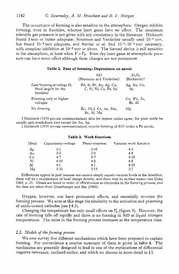
The dependence on electrode material is different for the anode, to which form- ing is sensitive, and the cathode, which does not appear to affect forming. The forming of a device M,-I-M, may fall into one of three categories. In the first forming occurs readily and at the same voltage whether MA or M, is the anode. In the second forming occurs only at higher voltages when one electrode (say MB) is the anode than at the usual forming voltage. The third class will not form at all when one electrode (say M,) is the anode. In table 2 we list the various anodes together with the class of junction they give. Results are given for A1,0, (Hickmott 1965 b) and S i 0 (Simmons and Verderber 1967 a). The S i 0 results are listed in order of ease of forming, measured by the time needed to form and the degree of forming. The A1,0, list is chosen to parallel the S i 0 one. It is clear that the general division is much the same in the two lists. Elements with high work functions that do not readily form stable oxides or fluorides generally give easy forming. In other instances the oxide is gaseous, or will itself undergo forming. By any other standards the appearance of carbon and silicon in the first category is surprising (see table 3).
1142 G. Dearnaley, A. M . Stonelzam and D. V . Morgan
The occurrence of forming is also sensitive to the atmosphere. Oxygen inhibits forming, even in fluorides, whereas inert gases have no effect. The maximum tolerable gas pressure is not given with any consistency in the literature. Hickmott found 1 torr or better adequate; Simmons and Verderber usually used torr, but found torr adequate, and Barriac et al. find 10-5-10-8 torr necessary, with complete inhibition at lop3 torr or above. The formed device is still sensitive to the atmosphere, at least when V > V,. Even dry inert gases at atmospheric pres- sure can have some effect although these changes are not permanent.
Table 2. Ease of forming: Dependence on anode
S i 0 A1203 (Simmons and Verderber) (Hickmott)?
Ag, Au, Cu, Easy forming a t voltage VF Pd, Ir, Pt, Au, Ag, Cu, C, Si, Ni, CO, Fe, Sn fixed largely by the
insulator Sn
Forming only at higher voltages
No forming
CO, Pb, In, Bi, A1
Zn, Pb,$ Cr, In, Mn, M g Be, Al, Mg
t Hickmott (1970 private communication) data for impure oxides agree; for pure oxide he
$ Hickmott (1970 private communication) reports forming of Si0 under a Pb anode. usually gets breakdown first except for Au, Ag.
Table 3. Work functions
Metal Capacitance-voltage Photo-response Vacuum work function
Ag 5.1 5.05 4.3 Au 5.0 5 .O 4.8 c u 4.7 4.7 4-25 h' i 4.55 4.6 4.5 A1 4.1 4.1 4.25 Mg 3.35 3.15 3.7
Differences appear in part because one cannot simply equate vacuum levels at the interface; there will be a modification of local charge density, and there may be surface states-see Duke 1969, p. 21. Metals are listed in order of effectiveness as electrodes in the forming process, and the data are taken from Goetzberger and Sze (1969).
Oxygen, however, can have permanent effects, and essentially reverses the forming process. We note at this stage the similarity to the activation and poisoning of oxide-coated cathodes (see 94.3).
Changing the temperature has only small effects on V, (figure 9). However, the rate of forming falls off rapidly and there is no forming in S i 0 at liquid nitrogen temperatures. The noise in the forming process increases as the temperature rises.
2.2. Models of the forming process We now survey five different mechanisms which have been proposed to explain
forming. For convenience a concise summary of them is given in table 4. The mechanims are generally designed to lead to one of the explanations of differential negative resistance, outlined earlier, and which we discuss in more detail in $ 3 .

a;
Electrical phenomena in amorphous oxide $films 1143
z
r-'
3
0 3
Y
2
Y
2 LcI U

1144 G. Dearnaley, A. M . Stoneham and D. V. Morgan
Hickmott (1964 a, b) suggested that there were immobile neutral impurities in the insulator, with ionization energies of about half the bandgap. In the forming process the impurities are ionized by the Poole-Frenkel process, giving an impurity band roughly in the middle of the bandgap, together with surface charges which allow electrons to enter the crystal without thermal activation. The voltage, rather than field, dependence of forming appears because the ionization of the impurities becomes significant at
Thickness 420
.- P"4 I2 "iz E -80 -40 0 40 r [ * c ) 80 120 160 200
Figure 9. Forming voltage at various temperatures for a Au-SiO-A1 device (after Verderber et al. 1967).
Like the other authors, Hickmott confirms that forming is not the same as electrical breakdown, since breakdown occurs at higher voltages. The difficulties with this model lie in part in the features which are not explained explicitly, such as the dependence on atmosphere, the release of gas and the dependence on electrode, and in part that rather severe demands are placed on the impurity levels. The impurities must be sufficiently dense that a satisfactory impurity band be formed, and in the correct energy range for injection to occur without thermal activation. It seems surprising that these features could occur in all the very wide range of insulators studied (if indeed the mechanism is the same in all cases). This point is emphasized further because his model of differential negative conductivity also involves an additional impurity band.
Simmons and Verderber (1967 a) proposed that forming consisted of the injection of metal ions from the anode into the insulator. This gave a broad band of impurity states which allowed conduction. Their model explains the dependence on elect- rodes, since the energy spectrum of the impurity levels depends on which species of ion is injected. The temperature dependence of forming follows since the ionic mobility is temperature dependent. Further, by making assumptions about the distribution of ionic space-charge and the resulting fields it is possible to argue that forming should be voltage dependent; this suggests that 4% < E,/2. In more detail, T'erderber et al. (1967) argue that V, is that potential which (allowing for space charge) gives a non-zero injecting field at the insulator-metal interface. They show this gives
V, = 2 (metal work function) - (insulator electron affinity)
- (activation energy for unformed device). (2.7) On the one hand, the forming
process seems to show none of the dependence on preparation or on insulator thickness and on electrode ionic mobility which would be expected for the wide range of cases studied. Nor is the dependence on atmosphere satisfactorily treated.
The objections to this theory are twofold.

Electrical phenomena in amorphous oxide films 1145
More telling, however, is the fact that the concentration of injected ions can be measured by Rutherford back-scattering. This is particularly straightforward for Au-SiO-Si devices, and shows that the Au concentration is at least a factor of 30 below that necessary for this theory (Dearnaley et al. 1970).
Dearnaley developed a filamentary model of forming. He argued that since the anode-insulator interface is not completely smooth there will be places where the electric field is particularly high. Near these places a structural change in the insulator occurs, giving a conducting filament. The electric field in the insulator near to the tip of the filament will be especially high, so that the conducting filament can propagate through the insulator until it forms a conducting link between the electrodes. This theory predicts a voltage-dependent forming if the initiation of the filament is a localized phenomenon and requires a higher electric field than the propagation of the filament, once initiated. Suppose the region in which initiation occurs at the electrode-insulator interface has a radius of order R. If the insulator thickness is d, then the electric field at the boundary of the region is
E ( R , d ) = E ( R , d = a) 1+-+ ... i "d" i where 7) is of order unity and depends on the detailed structure of the interface. The observed dependence of V, on d then allows an estimate of R, and the data in figure 7 suggest R v 20 8. The filaments would be hard to detect microscopically. The temperature dependence of the forming rate follows naturally, since the structural changes involve thermally activated ionic motion. The gas emission also occurs if the structural changes are electrolytic, and the dependence on ambient atmosphere is presumably a consequence of the equilibrium of the electrolytic reaction being affected. The dependence on the electrode results from the reaction of the gas released (usually fluorine or oxygen) with the anode to form a layer which prevents further filaments being started. Thus, as observed, the less reactive elements are the best anodes.
However, it is hard to see immediately what microscopic picture of the filament should be adopted so as to give the observed conductance. Conduction along . . . S-0-Si.. . chains via .n-electron overlap was originally suggested for S i 0 (Dearnaley 1967, Revesz 1967), but clearly this cannot be extended to all the systems which exhibit forming. A defect configuration, . , , M - ~ - M - ~ . , , consisting of alternate anions and cation vacancies was also proposed (Dearnaley 1969, Greene et al. 1969). It is feasible that conduction then takes place by hopping between adjacent localized anion sites-this phenomenon would be the (more-or-less) one-dimensional analogue of the Mott insulator-metal transition (9 1. l), and might satisfactorily account for the low activation energy. There are some similarities between the model of Dearnaley et al. and that of Gibbons and Beadle (1964), proposed to explain switching in thin NiO films. In the latter case, however, a single filament consisting entirely of metallic nickel was considered to form in the oxide-switching occurs but negative resistance does not result in this case. In the model of Dearnaley et al., very many filaments are postulated to develop at nucleation sites at the anode interface: this is feasible as long as (i) each filament introduces only a small change in the circuit resistance, and (ii) the applied voltage exceeds the forming voltage, V,.
Greene et al. (1969) argued that the forming mechanism is a high-field electro- lytic process in which anion vacancies are injected into the insulator. These vacancies give rise to localized conduction paths through the layer. At low fields the

1146 G. Dearnaley, A. 11.1. Stoneham and D. V. Morgan
reactions at the (assumed inert) electrodes for an insulator MX are X- - X + e- (anode)
M++e-- M (cathode) with the anions given off as gas. ,4t high fields a further cathode process occurs:
(X vacancy) +e - - - -+ (X vacancy with trapped electron) and vacancy injection results. Since atomic transport is involved the forming rate should decrease with temperature, as observed. Moreover, the forming voltage, V,, should be related to a Gibbs free energy of formation, as is shown in table 1. The dependence on electrodes can be explained by noting that if the anode is reactive, the insulator can grow at the anode through combination of insulator with anions with the electrode, and this can interfere with subsequent forming. The interference of an oxygen atmosphere follows from the existence of other competing cathode reactions, such as
$02 + 2e- ---+ 02-. Greene’s model accounts rather well for the forming in ionic crystals. It is not clear if the mechanism can be adapted to other insulators, such as SiO,, which show forming.
The model of Barriac et al. (1968) involves the injection of ions from the anode, giving the ionic conduction and space charge needed for their mechanism of differ- ential negative resistance. The injection is initiated by a local fusion of the insulator and electrode by a spark with large heat release. Electron traps are also created during the forming process that can only trap electrons when there is a sufficient electric field. The influence of the atmosphere arises because the oxygen can permanently neutralize the ions which constitute the space charge. This model suffers from the objections to ion injection which were mentioned in connection with the Simmons-Verderber model. It also leaves questions unanswered, such as the nature of the electron traps, and the dependence of V, on the electrodes and on the insulator.
3. Conduction, switching and memory phenomena The formed metal-insulator-metal device shows N-type differential negative
resistance and, associated with this, may be switched between states of different conductivity. We first survey the experimental data, and then review the various models which attempt to explain these conduction phenomena.
3.1. Observations of conduction, switching and memory phenomena We begin by considering the low-frequency current-voltage characteristics
(frequency< 100 Hz for SiO). As the voltage increases from zero the characteristic passes through several stages
(i) The current increases with voltage rather faster than expected from Ohm’s law.
I K Io sinh (Simmons and Verderber)
I cc Io(;)z (Hickmott)
where I, and V, are constants.

Electrical phenomena in. amorphous oxide jilms 1147
(ii) The current goes through a maximum at a voltage V,,, and then shows differential negative resistance. The decrease in current is roughly exponential in voltage. The current is then very noisy, the current fluctuations being as much as loyo, as opposed to 1% or less in other voltage regions.
(iii) The current passes through a minimum at Vmin, and rises slowly as the voltage increases. Ultimately dielectric breakdown occurs over the whole device. As the voltage is reduced the current follows essentially the same characteristic as before, sometimes with slight hysteresis and sometimes with a slight displacement of V,,,. The current characteristic is more or less symmetric in a formed device, and does not depend on which electrode is biased positive. This is also true of the switching and memory phenomena treated later. Figure 10 shows typical char- acteristics for SiO.
“min
Figure 10. Current-voltage (I-V) characteristics of a formed SiO, device for increasing and decreasing voltage sweeps (after Simmons and Verderber 1967 a).
The various memory states of the device may be achieved by applying a voltage V > V,,,, and then reducing the voltage rapidly. For S i 0 times of less than s are necessary. The conductivity is then fixed by the voltage prior to switch-off. This is shown in figure 11. The new current-voltage characteristic is essentially permanent provided the voltage does not exceed V,, which is rather less than V,,, and characteristic of the insulator. The memory state is long-lasting (it lasts for at Ieast two years) and is stable against mild heating and optical illumination, It can be erased by applying a voltage in excess of V,, when the current rises in steps to the original characteristic (figure 12). The current in the memory states can be varied continuously by a factor up to 1000.
The switching to and from the memory state can be rapid. A pulse longer than lO-’s is needed to switch from the high impedance (low current) to the low impedance state in SiO. The reverse process, from low impedance to high, can be

1148 G. Dearnaley, A. M - Stoneham and D. V . Morgan
achieved with a pulse of only 2 x s. However, the device cannot be cycled at a frequency corresponding to the longer time. There is a ‘dead time’ which must elapse before the device can be returned to the low impedance, high current state. The dead time, T,, varies with temperature and details of manufacture; it is usually in the range 10-1-10-6s. The recovery process associated with it is thermally activated, the activation energy being in the range 0.5-1.25 eV. Consequently at
Original
I
Switch off V
“T
Figure 11. The high- and low-impedance memory states which can exist, up to a threshold voltage VT, for a formed metal-oxide-metal structure.
l O m A
l O m s I
Figure 12. Step-like increase of current (I) as a function of time ( t ) in the switching of a formed SiO, film (after Greene et al. 1969).
very low temperatures, it is very difficult to switch the device from its high imped- ance, low current state. The characteristic for V < V, is very little affected, even at temperatures down to a few degrees K (figure 13) and the changes seem to be due to changes in the populations of the electron states near the Fermi level of the electrodes.
As the frequency of the applied voltage is raised the hysteresis of the current- voltage characteristic increases. The peak voltage and current also change (figure 14). The differential negative resistance disappears, usually between v = 100 Hz and v = 1000 Hz, giving a steady-state conductance which depends on the voltage amplitude. This is shown in figure 15.
In table 5, we collect together observed values of V,,,, Vmin and V, for a number of systems. Hickmott has observed two correlations :
V,,, x (energy gap in eV)*:z V V,,, 2: (10.3 - 0.18 [dielectric ~ons tan t ] )~ I~ V.

Electrical phenomena in amorphous oxide films 1149
0.1 0.2 0.3 0.4 0.5 0.6 5 (VI
Figure 13. The low-voltage conductivity of an Al-Si0,-Au device at temperatures of (A) pumped helium, (B) liquid helium, (C) liquid nitrogen and (D) room temperature. The oxide thickness is 400 A (from Hickmott 1971).
+--=loo
0 001 0.1 I 5 IO 100 200
I I I I / I I 0.01 0.1 I 5 I O 100 *do
N (Hz)
Figure 14. The variation in the maximum current, Ip, and the corresponding voltage, Up, as a function of frequency, N, in a formed Ag-Al,O,-Al structure. The subscripts a and r denote increasing and decreasing current, respectively (from Barriac et al. 1969).
46

1150 G. Dearnaley, A. M . Stoneham and D. V . Morgan
V
Figure 15. Broken line: the dc or low-frequency current-voltage (I-V) characteristics of a formed Au-Si0,-A1 device. Solid lines: the ac (1 kHz) characteristics of the same device for several voltage amplitudes (after Simmons and Verderber 1967 a).
Table 5.
Device Source VT V,,, Al-SiO-Au H 3.1
Pb-SiO-Pb H 3.0 Al-AlZOa-Au H 3 2.9
sv 2.9 4-5
Al-Al,O,-Ag B 4 Ta-Ta,O,-Au H 2.2 Zr-ZrO 2-Au H 2.1 Ti-Ti0,-Au H 1 *7
H -Hickmott. SV-Simmons and Verderber. B -Barriac et al.
K i n
8-9 8
7.2
8 5-6 4-5
3 . 5 4
7.5-8.5
0 2 4 6 8 1 0 < l / Z
Figure 16. The dependence of the voltage (V) for maximum current flow through formed metal-oxide-metal structures on the dielectric constant ( E ) of the oxide (after Hickmott 1971).
These correlations are not entirely independent, since the dielectric constant and bandgap are related by
The correlations are shown in figure 16 and table 6. The various voltages are

Electrical phenomena in amorphous oxide films 1151
independent of insulator thickness. Hickmott has verified this, for example, for A1,0, films in the range d = 150 to 1000 8.
Table 6. Dependence of V , on insulator band gap
Insulator I/;,(volts) ?&*(volts2) E,(eV) AI-SiO-Au 2.9-3’1 8 ‘4-9‘ 5 - Al-Al,O,-Au 2.8-2.9 7.9-8.4 (8.4) Ta-Ta,O,-Au 2-2 4.8 4.6 Zr-Zr0,-Au 2.1 4.4 (4.3) Ti-Ti0,-Au 1 *7 2.9 3.0 Nb-Nb,O,-Au 1.7 2.9 3.4
3.2. Theories of switching and memory in OxideJilms Our discussions of forming and of differential negative resistance showed that
there were as many theories as there were groups working in the field. The same is true of the conduction phenomena. We review the models in turn. The results are summarized in table 7 .
Hickmott’s model of conduction invokes space-charge limited conduction in an impurity band near the middle of the bandgap. The differential negative resistance is produced by some mechanism (ionization of another set of impurity levels has been suggested) which depends on a high field and which reduces the number of impurity states which contribute to the conduction. The mechanism must be temperature independent and with a short time constant. The re-formation of the impurity centres as the voltage is decreased has a longer time constant, and it is this longer time constant which determines the range of frequencies over which negative resistance may be observed. The processes he discusses are shown in figure 17. Switching and memory effects are not discussed by Hickmott, but the natural extension of his ideas would suggest that these phenomena arise from redistributions of electrons over the various impurity and band states. However, such a model would be open to objections which apply to all models which do not involve atomic rearrangement-the memory state lasts for several years without significant decay, and it is hard to see that a nonequilibrium charge distribution could exist for so long in a thin-film device.
Simmons and Verderber also proposed a mechanism without atomic rearrange- ment. The differential negative resistance resulted from the top of the impurity band falling below the Fermi level of the injecting electrode, thus inhibiting hopping conduction at constant electron energy across the device. In our earlier description of this process we ignored band-bending from the presence of space charge for simplicity of exposition. I t is essential to include these effects in their model of switching. Their description of band-bending assumes a broad distribution of electron traps with density n(x, E ) per unit energy range and unit volume, where x measures distance through the insulator. These states are not populated uniformly in space, and the local deviations from charge neutrality give the space charge of interest. We shall discuss the resulting potential when there is no bias voltage and when the Fermi level E, lies within the impurity band. The local deviations from charge neutrality are
ep(x) = /::dE n(x, E ) - (space-averaged charge density). (3.1)
45*

1152 G. Dearnaley, A. M . Stoneham and D. V. Morgan
ti ti ti d
2 % r .- 3
p1 z
U
i CI

Electrical phenomena in amorphous oxide films 1153
+A"
Unformed diode
Formed diode
Figure 17. Schematic illustration of conduction processes in the high-field region of a metal- oxide-metal structure (after Hickmott 1964 b).
But the effect of the space charge is to produce a potential V(x) which simply shifts the energy levels, and so displaces n(x, E ) in energy:
n(x, E ) -+ n(x, E + V(x) ). (3-2) If we now assume n(E) has a square distribution, that is n(E) = N within the impurity band and is zero outside, then
ep(x) = eNV(x) +constant terms. (3.3) Substituting into Poisson's equation,
d 2 V eN - = - V + constant terms dx2 E
so that
V(X) = Aexp (fj - +Bexp (-E) + constant
in which
(3.4)
(3.5)
and A and B are fixed by the boundary conditions. If the device is symmetrical and the barrier thickness d x, then

1154 G. Dearnaley, A. M . Stoneham and D. V. 1Worgan
Thus the band structure is as shown in figures 18 and 19. The bands bend down- wards because of the (attractive) defects in the insulator. Simmons and Verderber quote N = lOI9 ~ m - ~ (with an impurity band width of 3 17) which, with E = 4, gives x12: 50 8 ; this may be compared with the insulator thickness of several hundred Angstroms.
Metal
b a n d ‘ F e r m i level
Figure 18. Band bending of the energy levels at a metal-insulator boundary when the applied voltage is zero and the Fermi level lies within the impurity band. Local deviations from charge neutrality give rise to a space charge. The bands bend downwards due to attractive defects in the insulator.
When the applied voltage V exceeds V,,,, electrons injected at energies near E, hop between impurity states close in energy and are trapped in the depletion layer, since transitions to traps of very different energy are considered improbable. If the applied voltage is rapidly reduced, this charge does not return to the electrode from which it came, but moves by a thermally activated process to the centre of the insulator. This electronic space-charge reduces the conductivity of the device, as in the memory state. The memory state can, of course, be removed by removing the stored charge. The processes are shown in figures 20 and 21. The rate of switching is limited by the mean hopping time, TH from trap to trap. If T~ is short compared to the time in which the applied voltage V is reduced from above V,,,, the space charge can trickle back to the nearest electrode; the space charge follows the field roughly adiabatically. However, if T~ is long compared with the voltage reduction time the charge does not move significantly until after the reduction is complete, when the fields now favour a movement of charge to the centre of the insulator. The dead time is also TH. Since T~ involves thermal activation, we can also under- stand the temperature dependence of these processes. Simmons and Verderber postulate that the normal (high current) behaviour, which also involves hopping, does not show thermal activation because transitions between sites with the same energy (that is, with zero activation energy) are dominant. This hypothesis does not seem to be consistent with the general arguments of Mott (Mott 1967, especially p. 71) who argues that
(3.7)
in which wH(r) is a ‘tunnel factor’ depending on the separation of the two sites
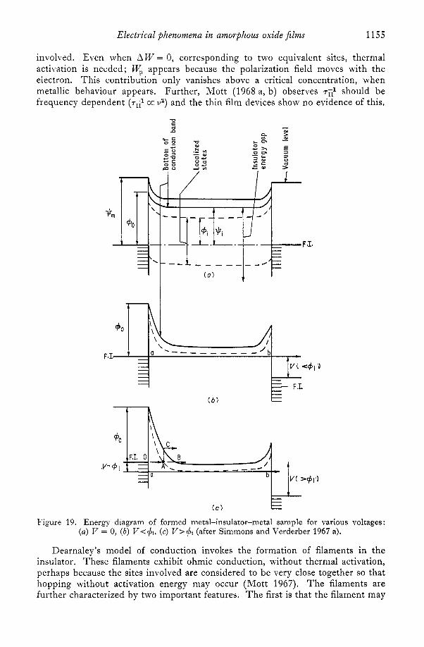
Electrical phenomena in amorphous oxide films 1155
involved. Even when A W = 0, corresponding to two equivalent sites, thermal activation is needed; W, appears because the polarization field moves with the electron. This contribution only vanishes above a critical concentration, when metallic behaviour appears. Further, Mott (1968 a, b) observes T E ~ should be frequency dependent ( T G ~ K I?) and the thin film devices show no evidence of this.
-0
0 - c 01 n. n
ks U ,g .2 - 0 1 2 % E
OFII a gs gbl - 4-0 c l c OS = k z 0 0 0"s - 2 5 g m v ~m
R
Figure 19. Energy diagram of formed metal-insulator-metal sample for various voltages : (a) V = 0, ( b ) V<$i, (c) V>$i (after Simmons and Verderber 1967 a).
Dearnaley's model of conduction invokes the formation of filaments in the insulator. These filaments exhibit ohmic conduction, without thermal activation, perhaps because the sites involved are considered to be very close together so that hopping without activation energy may occur (Mott 1967). The filaments are further characterized by two important features. The first is that the filament may

1156 G. Dearnaley, A. 1Vl. Stonehain and D. V . Morgan
Figure 20. Energy diagram showing the position of the stored charge relative to the Fermi level: (a) at a voltage bias of Z' volts, (b) immediately after voltage has been rapidly reduced to zero, ( c ) after a longer time interval (after Simmons and Verderber 1967 a).
Figure 21. Energy diagram showing the position of stored charge relative to the Fermi level: (a) before switching occurs, (b) at onset of switching (after Simmons and Verderber 1967 a),

Electrical phenomena in amorphous oxide jilms 1157
fracture and cease to contribute to the conduction; the second is that the filament can re-form under suitable conditions. Detailed atomic models of these processes are still speculative, but it is clear that the re-forming will be related to the basic forming process of propagation of the filament through the insulator. The fracture of the filament is probably a consequence of Joule heating, raising the temperature of a part (at least) of the filament so that there is local atomic reorganization, as in melting or other phase changes. In addition, the phonon scattering of electrons also increases as the filament temperature rises. We shall see that the fracture is probably localized in some small region of the filament, since then the switching is voltage, rather than field-dependent. The localization of the fracture results from the nonuniformity of the filaments, which are postulated to have weak spots, a consequence of their growth and the amorphous nature of the insulator.
We now consider the current-voltage characteristics of an array of conducting filaments embedded in an insulating matrix. Each filament will be assumed to exhibit ohmic conduction and we will ignore hopping conduction, tunnelling and space-charge effects which probably play a role; by ignoring these effects we shall be unable to predict the nonlinear dependence of current upon voltage at very small voltages. The novel current-voltage characteristics occur because filaments can rupture.
Once each filament bridges the gap between the electrodes, electronic conduc- tion begins and Joule heating will occur. We then associate a local lattice tempera- ture T with each filament and assume that rupture will occur if T exceeds T,,,. The filaments can re-form subsequently, but this will depend on their temperature, the ambient temperature, the electric field and possible space-charge effects ; the precise conditions will not be specified in detail. The filament temperature, T is not a thermodynamically well-defined quantity. I t will only be used as a measure of the local heating in the filament. Physically both T and the resistance p of each filament can best be imagined by associating them with local regions of high resistance on a highly conducting filament or chain of defects. Two terms con- tribute to changes in T, one due to the usual Joule heating and the other to heat loss to the insulator, which we assume simply to be proportional to the temperature difference between the filament and its environment. Thus the local temperature is given by
d T Vz(t) 1 - = .---(T-T,) dt P 7 0
where 01 measures the heating and T~ characterizes the cooling.
(3.8) we see that, at voltage V , only filaments with resistance greater than We first consider the static characteristic. From the steady-state solutions of
remain unfractured. The total current is thus
where P(p) gives the probability distribution of the various resistances, and
p P W = 1.
(3.10)
(3.11)

1158 G. Dearnaley, A. M . Stoneham and D. V, Morgan
We have assumed implicitly that the filaments are either permanently broken or permanently unbroken at the given voltage, and that an equilibrium has been achieved so that the previous history of the specimen can be ignored. Clearly the detailed shape of the characteristic is determined by the distribution P(p). Two features of P(p) are immediately apparent. First, there are very few filaments with resistance below
(3.12)
since the devices can be cycled below yT without showing signs of filaments breaking.
/ \
Figure 22. (a) The calculated distribution of filament resistances, p , deduced from experi- mental current-voltage behaviour. Negative values near the origin arise because tunnelling at the electrodes has been neglected. (b) The simple triangular distribution of filament assumed as an approximation in fitting the current-voltage characteristic (after Dearnaley et al. 1970).
Secondly, there are very few filaments with resistances above
(3.13)
where V , is the voltage at which I( V) is a minimum. Above V , the conductivity is small, and the filamentary contribution cannot be appreciable. We can derive P(p) from I ( V ) by noting
(3.14)
this distribution is shown in figure 22. The apparently negative value of P(p) for small p simply reflects the contribution of tunnelling or space-charge effects at small voltages. The absence of very low-resistance filaments is just a consequence of finite specific resistance; the absence of very high-resistance filaments presumably reflects a natural selection mechanism in the forming process; that is to say that a filament will cease to propagate rather than continue as high-resistance path, if conditions (such as the local structure of the insulator) are unfavourable.

Electrical phenomena in amorphous oxide films 1159
The distribution of resistances shown in figure 22 is merely qualitative unless we can estimate N, the number of filaments per unit area. We now make a rough estimate of N assuming that all filaments have the same resistance, i. The initial resistance of the device per unit area is p/N, apart from small tunnelling effects, and the filaments all burn out when V > V,,,. Thus, from equation (3.8),
(3.15)
The cooling time, T ~ , is estimated by regarding each filament as a cylinder of radius R and temperature T cooling to a cylindrical sink radius D and temperature T,; D is taken to be the mean filament separation defined by ND2 = 1. It is then easy to show that
(3.16)
where K is the thermal conductivity of the insulator and L is the length of the filaments. Note that the choice of D and R is not very critical in this equation. Combining (3.15) and (3.16) we may find p and N. Reasonable values of most of the parameters are easily introduced, e.g. an initial resistance p / N of 5 s1 for a filament length of 400 8, a thermal conductivity of 0.002 cal cm-2 s-l K-l and (Tma,- T,) of 1000 K. It is harder to estimate R, but our earlier discussion of the dependence of forming voltage upon film thickness suggests R 2: 10 8. Using these values we find p , the mean resistance per filament, to be about 2.5 x lo7 s1 and N to be 5 x lo6 filaments per cm2. These lead to D 2: 2.5 pm and a specific resistance of about 0.2 ohm cm for the material of the filament. We emphasize that these calculations give only order of magnitude estimates since, for example, end effects have been neglected in deriving T ~ . However, the results appear to be both plausible and consistent. We have since learned that microphotographs of formed silicon monoxide films (R. Hall, private communication) do in fact reveal about lo6 minute holes per square cm in close agreement with our estimate.
We now turn to consider the dynamic characteristics of formed devices, in much the same manner as the dc behaviour was treated. If the applied voltage has ampli- tude V,
V = V,sinwt (3.17)
then after a time of order T~ when the transients have disappeared, the filaments with resistance greater than
Pmin(w, V,> = PInin(0, V,) 4(w, ~ c ) (3.18)
remain unfractured. Here pmin(O, V,) is equivalent to (3.9), and
4(w ,TC) = $[I +{I +(2Tc)2)-1’2]. (3.19)
At higher frequencies more filaments survive. The current is given by
(3.20)
wheref(p, w ) is the fraction of the time for which a filament of resistance p operates at frequency W . Clearly f(p, w ) is unity if p is greater than pmi,(w). The dynamic characteristic differs from the static characteristic in that the filaments which are broken re-form only after a number of cycles, and the conduction is dominated by
1160 G. Dearnaley, A. M . Stoneham and D. V. Morgan
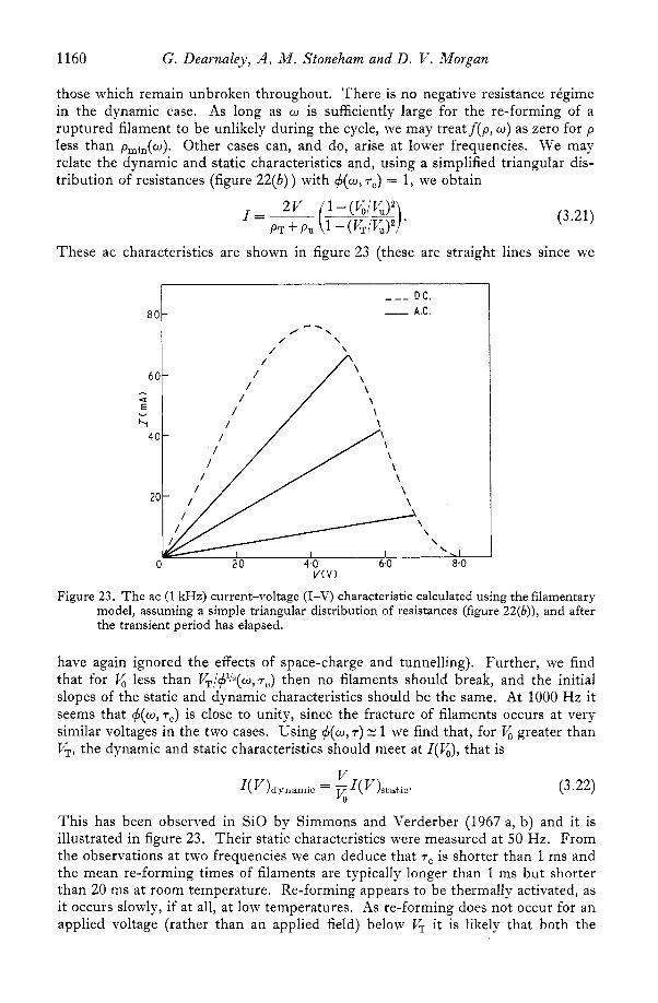
those which remain unbroken throughout. There is no negative resistance rCgime in the dynamic case. As long as w is sufficiently large for the re-forming of a ruptured filament to be unlikely during the cycle, we may treatf(p, U ) as zero for p less than pmin(w). Other cases can, and do, arise at lower frequencies. We may relate the dynamic and static characteristics and, using a simplified triangular dis- tribution of resistances (figure 22(6)) with ~ ( u , T ~ ) = 1, we obtain
(3.21)
These ac characteristics are shown in figure 23 (these are straight lines since we
_ _ _ D.C. - A.C.
/ --, / \
Figure 23. The ac (1 kHz) current-voltage (I-V) characteristic calculated using the filamentary model, assuming a simple triangular distribution of resistances (figure 22(b) ) , and after the transient period has elapsed.
have again ignored the effects of space-charge and tunnelling). Further, we find that for y0 less than J $ / r , b l / ~ ( w , ~ ~ ) then no filaments should break, and the initial slopes of the static and dynamic characteristics should be the same. At 1000 Hz it seems that ~ ( W , T ~ ) is close to unity, since the fracture of filaments occurs at very similar voltages in the two cases. Using +(U, T ) 1: 1 we find that, for V, greater than V,, the dynamic and static characteristics should meet at I(%), that is
(3.22)
This has been observed in S i 0 by Simmons and Verderber (1967 a, b) and it is illustrated in figure 23. Their static characteristics were measured at 50 Hz. From the observations at two frequencies we can deduce that T~ is shorter than 1 ms and the mean re-forming times of filaments are typically longer than 1 ms but shorter than 20 ms at room temperature. Re-forming appears to be thermally activated, as it occurs slowly, if at all, at low temperatures. As re-forming does not occur for an applied voltage (rather than an applied field) below V, it is likely that both the
V I(V)dynamic = -I(V)static* v,

Electrical phenomena in amorphous oxide films 1161
fracture and the re-forming only involve a well-localized region of space. After fracture the filament must be in one of several distinct states. The dead time, discussed earlier, is a measure of the time between the filament breaking and reach- ing a state from which it may re-form. This transition appears to be thermally activated.
One possible microscopic model which predicts a dead time is the assumption that, during the rupture of the filament at a weak spot, electrons are scattered into the surrounding matrix. The insulator will be highly polarized locally and will return to equilibrium by thermally-activated processes, such as Poole-Frenkel emission from traps. At low temperatures this ‘polarized’ state will exist for a long time, and re-forming will not occur. At higher temperatures the system may relax rapidly to a state in which the filament is broken but the polarization is absent. The filament may then regrow by ionic migration in the electric field. The relaxation will take a finite time and hence we can explain the transient phenomena which appear at frequencies between 50 and 1000 Hz. Furthermore, filaments which have been broken remain nonconducting for almost the whole of the time since the time constant for the heating process is short compared with the time to re-establish conduction. I n this way we can understand the relatively long switching time from the high to the low impedance state (of the order of lO-‘s) while switching back to the high impedance state is rapid (of the order of s). I t is likely that the differ- ence occurs because in the former case ionic migration must take place, while in the latter the controlling mechanism is the scattering of ‘hot’ electrons leading to polarization of the dielectric. Likewise, we can understand why the ‘dead time’ of many milliseconds must elapse before the cycle can be repeated-this corresponds to the relaxation of space-charge polarization.
Barriac et al. (1968, 1969) argue that the differential negative resistance in dc characteristics results from a combination of ionic and electronic conduction. They do not discuss switching.
Their analysis of the dc characteristic divides the voltage into four regions- regions A and B below the maximum current, and regions C and D when there is differential negative resistance. Ionic conduction alone is important below the voltage for maximum current, V,,,. In this regime
I = A exp (aV) (3.23)
where A N A,exp ( - U,/kT) , U, being an activation energy and A, the diffusion length (the diffusion coefficient is D = A: v exp (- U,/kT), A, being the site separation multiplied by an entropy factor). The parameter a: depends on temperature and the thickness of the depletion layer
(3.24)
where q is the ionic charge. The dependence on the potential V is complicated because 6 is a function of V , At the lowest voltages (region A), 6 changes rapidly with V , saturating to a value A independent of V to give region B. This is illustrated in figure 24. Thus below V,,, the current is a space-charge limited ionic current. Once V reaches V,,, electrons begin to tunnel into the insulator through the electrode barriers. The electrons in turn are trapped within the insulator to form immobile defects, thus reducing the electronic and ionic currents. The reduction of the current (basically the loss of ionic current, assuming all electrons are trapped)
46

1162 G. Dearnaley, A. iW. Stoneham and D. V. Morgan
is then
(3.25)
which is the usual Fowler-Nordheim expression. B and ,B both depend on 6(V) and also on the height of the metal-insulator barrier. As the ionic space-charge becomes increasingly neutralized the depletion layer starts to increase in thickness from A once more, giving the transition to region D from region C.
I
V-
Figure 24. The dependence of the parameter 8 on the potential V, in the theory of Barriac et al. (1969). At low voltages 8 changes rapidly with V, but saturates to a value A.
The traps are assumed to have a mean trapping time T which is temperature- dependent, and the neutral units of an electron and ion are assumed unstable in the absence of a field. The hysteresis seen in the characteristics at low frequencies is a direct result of trapping. Finally, the effect of oxygen is to give a permanent neutralization of the ions which give rise to the space charge, so explaining the sensitivity to the atmosphere.
One prediction of this model is the value of the voltage of maximum current. The current is the sum of two terms:
I = Aexp(cxV)-BV2exp __ 3 (3.26)
and V,,, is readily found from the zero of (aljaV). The result leads to a major disagreement with experiment. Both A and 01 depend on temperature, so that V,,, is sensitive to the temperature. But V,,, is observed to be essentially temperature- independent from helium temperatures to above room temperature. Thus both on this point and on the earlier objections to models invoking ion injection it seems unlikely that the Barriac-Pinard-Davoine mechanism is correct.
Greene et al. do not discuss the switching or conduction mechanisms in detail, but suggest they involve trapped space charge produced when the applied voltage is sufficient to give some electrons enough energy to leave the conducting path and enter the surrounding unformed dielectric.
3.3. Observations on triodes The experimental data discussed so far all refer to diodes, that is to two-
electrode metal-insulator-metal devices. Hickmott (1964 a, b) has made an important set of experiments on triodes, or three-electrode devices. The structure he used is shown in figure 25.

Electrical phenomena in amorphous oxide films 1163
Before forming, the electrical behaviour of the triodes is orthodox, and the potentials applied between the plate and cathode divide as expected between the plate-grid and grid-cathode regions. However, after forming the potential dis- tributions are highly nonlinear (figure 26). Nearly all the potential drop occurs at the negative electrode, between grid and cathode. When the voltage is reversed the potential drop remains in the same region, although the high conductivity and differential negative resistance are still observed. The high-field region can be shifted to between the plate and the grid; this does not affect the plate-cathode characteristics greatly provided that a high-field region remains somewhere in the device.
1 Cathode ( A L ) I Figure 25. The metal-oxide-metal-oxide-metal triode structure.
Vocuum
Vapplied lJ ( A I ) ( A l l Plate ( A I 1
Figure 26. Schematic representation of the potential distribution in oxide triodes after develop- ment of plate-cathode conductivity (after Hickmott 1964 b).
Thus the high conductivity is not a consequence of field emission at the cathode from this high-field region. The potential in the low-field region is linear in the current in that region; that is, conduction is ohmic.
One remarkable feature is that the development of conductivity between plate and cathode (the forming) does not necessarily result in conductivity to the grid. Grid conductivity may be developed separately or it may develop during the establishment of plate conductivity. In one device, for example
and
whereas when the voltage is applied from cathode to plate Rbg = &,/IPc-22 ohms. We know of no satisfactory explanation of these phenomena.
R,, = Jig/IPg > 2.10j ohms R,, = V,,/I,, > 2.105 ohms
4. Electron emission, luminescence and other phenomena We now consider some of the effects of forming other than those on the current-
voltage characteristic. In particular, formed devices are rather efficient electron emitters, the emitted current being up to 1% of the current in the device in some cases. Other related phenomena are electroluminescence and the noise in the device.

1164 G. Dearnaley, A. M . Stoneham and D. V. Morgan
I I
4- I I
(U) t
4.1. Electron emission The electron emission from a formed device depends strongly on the voltage.
At voltages below V,,, there is very little emission, but a sharp rise occurs at V E V,,,. As the voltage is further increased the emitted current either rises slowly, as with the Al-SiO-Au device (see figure 27) or decreases, as with the A1-Al,03-(A1
Figure 27. Curves showing the circulating current and emission current as a function of applied voltage in a formed Au-SO,-A1 device (after Simmons and Verderber 1967 b).
V ( V )
Figure 28. The circulating current (It) and emission current (I,) as a function of applied voltage for (a) a Au-A1203-A1 device and (b) an A1-Al2O3-A1 device (after Barriac et al. 1969).
or Au) device (see figure 28). The emitted current then starts to increase again at a voltage near to the work function of the electrode through which emission occurs. The detailed behaviour depends both on the nature of the insulator (Hickmott 1963) and, to some extent, on its thickness (Hickmott 1965 a). The emitted current may also show slight structure when eV is equal to the insulator bandgap; this appears in A1,03 and Ta,O,.
The emission is not uniform over the device and appears to come from small localized regions. There is some correspondence between the luminescent regions we discuss later, but there is not a clear one-to-one correspondence between the two.
Electrical phenomena in amorphous oxide jilms 1165
The emission is also temperature-dependent ; at lower temperatures the fraction of current through the device which is emitted decreases, the decrease being greater at lower voltages.
The electrode through which emission occurs also affects the observed external current. I n the simplest cases the current is simply attenuated; the attenuation length in gold being typically between 200 and 300 A, without strong dependence on the applied voltage. However, more subtle effects may be seen, particularly at lower voltages. These include the diffraction of electrons by pinholes in the electrode, which affects the spatial pattern of the emission (Verderber and Simmons 1966, Simmons and Verderber 1967 a, b). One of the reasons for the emission efficiency of these oxide devices as opposed to thinner films (10-50 A) which has been suggested is that higher voltages can be applied to thicker films without breakdown, and these higher voltages give emission with less attenuation by diffraction.
The important points in interpreting the emission data are these. First, a significant fraction of the emitted electrons have energies close to eV, where V is the applied voltage. Second, much of the emission is localized at small regions in the electrode. Third, the emission is not simply a result of the insulator becoming hot; Verderber and Simmons eliminate this possibility by observing that the electron emission does not follow the power dissipation in the device.
A number of phenomena which occur in conventional oxide-coated cathodes may be related to the effects we have been discussing. Thus the electron emission of such a cathode is low prior to ‘activation’, which consists usually of the applica- tion of an electric field to the cathode under conditions in which some of the oxide may be reduced. Oxygen is released during this process. The electron emission is seen (Hanney et al. 1949) to follow the growth of electrical conductivity through the oxide. Heinze and Wagener (1939) studied the distribution of the emission from an oxide cathode at successive stages of activation. They formed electron images of the cathode and thereby observed that emission takes place from small bright centres. Initially only a few centres were present but as activation proceeded the number of sites increased very greatly but their size varied little. Later Mecklenburg (1943) used projection-tube microphotography to demonstrate that these emission centres are less than 400 A in diameter and are distributed in a pattern related to the grain size in the oxide. I t appeared that the emission centres were grouped along grain boundaries in the microcrystalline oxide of the cathode. A characteristic of the oxide-coated cathode is the phenomenon of ‘flicker’ noise. This is a low-frequency electrical noise with a power spectrum showing a l/f a: frequency dependence, where a is about 1.0-1.5. This noise is a minimum if the cathode is well activated.
4.2. Electroluminescence in M-I-M (metal-insulator-metal) structures In this section, we consider electroluminescence which occurs inside the
insulating oxide as opposed to the electroluminescence in a semiconducting sub- strate (the M-I-s system of $4.4). Oxide films that develop voltage-controlled negative resistance (A1,0,, SiO, Ta,O, and ZrO,) have many features in common. Prior to forming, low-voltage electroluminescence in the near infrared has been reported in Ta-Ta,O,-Au (Hickmott 1966 a, b). However, visible electrolumine- scence develops simultaneously with the development of voltage-controlled negative resistance.

1166 G. Dearnaley, A. M . Stoneham and D. V. Morgan
In the formed oxide, the electroluminescence parallels electron emission to some extent. The luminescence first appears at voltages just below V,,,, and falls again in the differential negative resistance rCgime, before starting a slow rise in intensity with applied voltage. The light, which covers a wide spectral range, is emitted from a few bright spots; these spots are usually stable under repeated tracings of the current-voltage characteristic, although a few spots appear or disappear. The spots are typically a few microns across and there is no conclusive evidence that they are the spots from which electron emission occurs. The electroluminescence and its spectrum are shown in figure 29. Hickmott has analysed the spectra from A1-AI,O,-Au and Ta-Ta,O,-Au structures; one of the conspicuous peaks at about 4 eV for A1,0, could be related to the strong peak, extending from 3 .5 to 6.0 eV, observed in x ray induced luminescence (Runciman 1968) and attributed to iron impurity. However, atomic aluminium in its various charge states also has a number of bands in this range, and these have probably been detected in the breakdown of AI-SiO-A1 (Budenstein et al. 1969).
Electroluminescence is not confined to oxide films which develop voltage- controlled negative resistance. In anodically grown Zr-Zr0,-A1 diodes, for example, R'Iochniak (1966) has observed electroluminescence where the integral electro- luminescence intensity increases with the current density flowing through the oxide. The light appears for both the forward and reverse bias. Hickmott (1966 a, b, 1969 a, b) has studied in detail the electroluminescence in Nb,O, diodes which exhibit current-controlled negative resistance. The diodes are electroluminescent before forming; after the forming process, increased electroluminescence accom- panies switching and emitted light is both polarity- and voltage-dependent. Micro- scopic observations indicate that the forming and switching occur at small conducting regions.
I IP 21 photomultiplier
Figure 29 ( a )

Electrical phenomena in amorphous oxide jilms 1167
I IP 21 photomultiplier
0 2 4 6 8 1 0 V ( V )
Figure 29 (b)
Figure 29 (c)
Figure 29. (a) and (b) : the electroluminescent intensity at different wavelengths as a function of the voltage applied to a Au-Al,O,-Al structure. The oxide thickness was 550 A, the gold thickness 200A (after Hickmott). (c) Pen-recorder plot of the development of conductivity and of electroluminescence in an Au-AI,O,-A1 stucture. Current bursts at A, B, C coincide with flashes of light (after Hickmott 1971).
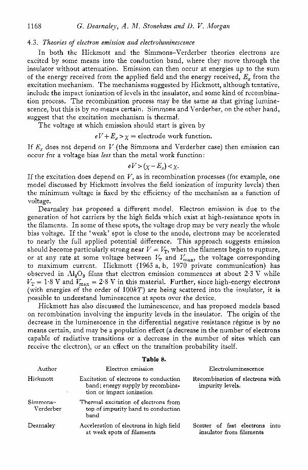
1168 G. Dearnaley, A. M . Stoneham and D. V . Morgan
4.3. Theories of electron emission and electroluminescence In both the Hickmott and the Simmons-Verderber theories electrons are
excited by some means into the conduction band, where they move through the insulator without attenuation. Emission can then occur at energies up to the sum of the energy received from the applied field and the energy received, E, from the excitation mechanism. The mechanisms suggested by Hickmott, although tentative, include the impact ionization of levels in the insulator, and some kind of recombina- tion process. The recombination process may be the same as that giving lumine- scence, but this is by no means certain. Simmons and Verderber, on the other hand, suggest that the excitation mechanism is thermal.
The voltage at which emission should start is given by eV+ E, > x = electrode work function.
If E, does not depend on V (the Simmons and Verderber case) then emission can occur for a voltage bias less than the metal work function:
eV > (x - Ez) < x. If the excitation does depend on V , as in recombination processes (for example, one model discussed by Hickmott involves the field ionization of impurity levels) then the minimum voltage is fixed by the efficiency of the mechanism as a function of voltage.
Dearnaley has proposed a different model. Electron emission is due to the generation of hot carriers by the high fields which exist at high-resistance spots in the filaments. In some of these spots, the voltage drop may be very nearly the whole bias voltage. If the ‘weak’ spot is close to the anode, electrons may be accelerated to nearly the full applied potential difference. This approach suggests emission should become particularly strong near V = V,, when the filaments begin to rupture, or at any rate at some voltage between V, and V,,,, the voltage corresponding to maximum current. Hickmott (1965 a, b, 1970 private communication) has observed in A1,0, films that electron emission commences at about 2.3 V while V, = 1.8 V and V,,, = 2.8 V in this material. Further, since high-energy electrons (with energies of the order of 100kT) are being scattered into the insulator, it is possible to understand luminescence at spots over the device.
Hickmott has also discussed the luminescence, and has proposed models based on recombination involving the impurity levels in the insulator. The origin of the decrease in the luminescence in the differential negative resistance rCgime is by no means certain, and may be a population effect (a decrease in the number of electrons capable of radiative transitions or a decrease in the number of sites which can receive the electron), or an effect on the transition probability itself.
Table 8. Author Electron emission Electroluminescence
Hickmott Excitation of electrons to conduction Recombination of electrons with band; energy supply by recombina- tion or impact ionization
Thermal excitation of electrons from top of impurity band to conduction band
at weak spots of filaments
impurity levels.
Simmons- Verderber
Dearnaley Acceleration of electrons in high field Scatter of fast electrons into insulator from filaments

Electrical phenomena in amorphous oxide jilms 1169
A model for the oxide-coated cathode analogues to the one developed to account for the behaviour of amorphous oxide films has been proposed by Dearnaley (1969). He suggests that the electronic conduction is developed during activation by filamentary propagation through the oxide, assisted by reducing conditions and temperature. The filaments are believed in this case to be a defect state, possibly a chain of alternate cations and anion vacancies, or surface F-centres, clustered along grain boundaries of the material (see also § 5.3). In this way the small emission centres are satisfactorily explained, together with the mechanism of ‘poisoning ’ of the cathode by oxygen. The high thermionic emission is explained by the field emission from such highly localized ‘patches’ coupled with the local Joule heating which is a consequence of conduction through filaments.
Metal I Semiconductor Metal Oxide Semiconductor
(01 ( b )
Figure 30. The electronic energy levels in (a) a metal-semiconductor and (b) a metal-oxide- semiconductor contact (after Jaklevic et al. 1963), illustrating the greater ease of tunnelling of holes brought about by the electric field in the oxide.
4.4. Injection electroluminescence in MOS (metal-oxide-semiconductors) structures The injection of carriers into suitable wide bandgap semiconductors has often
been studied as a potentially efficient means of generating electroluminescence, One method which has been used in studying this has been to deposit a thin film of S i 0 or CaF, on to a single crystal of semiconductor. Thus Jaklevic et al. (1963) deposited 50-15OA layers of SiO, on CdS and after forming of the oxide film, observed green electroluminescence at 77 K. If the oxide layer was omitted, no luminescence was seen. .It was noticed that the light originated at numerous tiny spots, distributed over the surface in a random manner, the smallest being less than 10 pm in diameter. These authors attributed the behaviour to hole injection by tunnelling through certain localized regions, the holes entering the valence band as indicated in figure 30. Some observations by other authors cannot, however, easily be attributed to tunnelling, even assuming the existence of ‘ pinholes’.
Fischer and Moss (1963) made a series of similar experiments with a range of materials, including CaF,, MgO, ZnF,, CdF,, on semiconductors. The layers on this case were as much as 500 A in thickness, yet tunnelling of carriers through the film was stili proposed as the injection mechanism.
Yee and Condas (1968) observed electroluminescence in MOS structures on CdS. An evaporated layer of SiO, several hundred Angstroms thick was employed, with

1170 G. Dearnaley, A. .MO Stoneham and D. V. Morgan
a gold layer deposited on top. High current densities (of the order of 30 Acm-2) were achieved in the dc mode, and the emission spectrum, while varying with injection current, showed several features characteristic of CdS emission. The carrier injection mechanism was not identified.
Ralph and Tansley (1970) have examined the behaviour of Au-CaF,-CdS and Tansley and Ralph (1970) Au-Si0,-GaAs diodes. Here, oxide and fluoride layers up to 5000 -4 in thickness were used without drastic alteration in device behaviour. While tunnelling seemed an unlikely mechanism in some previous work, this finding rules it out as an explanation of the injection process. The internal quantum efficiency of some of the structures used as photodiodes was very high (as much as 28% at 4800 *k). The Au-Si0,-GaAs diodes exhibited forward-bias electro- luminescence with a spectrum characteristic of radiative recombination on GaAs. Such emission demands the injection of holes into the n-type semiconductor. In addition a variety of switching and negative resistance phenomena was observed in the devices, dependent upon the nature of the anode metal.
It seems clear from the nature of the insulating films used in these experiments, their thickness and mode of preparation and the type of metal electrodes deposited on them, that phenomena similar to those we have discussed above will be occurring in the oxide (or halide) layer. The current densities are such as can only be explained if the layer is ‘formed’. The localized electroluminescence observed by Jaklevic et al. (1963) is very reminiscent of the localized conduction and emission phenomena we have already discussed. We shall now consider how the various models of con- duction and forming in oxides can account for these effects.
Hickmott (1964 a, b) has proposed that conduction and negative resistance in a thin oxide film are high-field phenomena, with a nonuniform potential distribution within the material. Xear the negative electrode, a high-field region between 100 and 150 A thick is believed to develop, and accounts for the electron emission and electroluminescence of metal-oxide-metal diodes or triodes. This same model could allow the injection of electrons or holes into a semiconductor if this were substituted for the cathode material. It is less easy to understand the process in terms of Simmons and Verderber (1967) although they present a clearer picture of the physical mechanisms taking part. The difficulty lies in the fact that energy loss processes in the insulator are likely to be dominant, and no mechanism is proposed whereby the carriers can gain energy efficiently enough.
Dearnaley et al. (1969) have proposed a filamentary conduction model, which immediately explains the localized electroluminescence observed by Jaklevic e t al. The size of the emitting spots will naturally be larger than the filament diameter, since minority carriers injected into semiconductor will have a certain mean free path before recombination. Since, in their model, the filaments are considered to possess weak spots at which the field is high, and undergo rupture at these points, conditions for efficient heating of carriers in localized high-field regions are met. Ralph (1970) has recently pointed out that, in the propagation of a filament from the anode towards the cathode, termination of the atomic rearrangements will naturally occur when the distance between the filament and the cathode is short enough (say, about 30 A) to allow tunnelling. Therefore, it is natural that a high- field region should exist very close to the cathode, and this may in turn explain some of Hickmott’s (1964) observations on the field distribution in oxide layers. The presence of a fine filament terminating in a high-field zone (figure 31) gives ideal conditions for the injection of hot holes into the semiconductor, and therefore the

Electrical phenomena in amorphous oxide $Ems 1171
possibility of efficient electroluminescence. If this is correct, the electrolumine- scence efficiency will tend to increase with the degree of forming of the oxide layer. This mechanism of injection resembles that proposed by Fischer (1963) as a means of creating hot carriers on ZnS crystals, by field emission from the tips of fine crystallites embedded in a structurally different matrix (figure 3 l ( b ) ).
Conducting U / needle
f i loment
U
U
U U
Metal oxide f i l m Semiconductor
Traps
( a ) (6)
Figure 31. The analogy between (a) the alternate field emission of electrons and holes from a conducting needle embedded in a luminescent medium subjected to an alternating electric field (after Fischer 1963) and (b) field emission of holes from the end of a conducting filament embedded in an insulating matrix, near to a semiconductor inter- face. In both cases, radiative recombination may take place at traps.
4.5. Noise The current-voltage characteristic of a formed metal-oxide-metal structure
shows very considerable noise fluctuations (of the order of 10%) in the region of differential negative resistance, and a related phenomenon may be of the step-like recovery from the high-resistance to the low-resistance state during switching.
These features were discussed by Dearnaley et al. (1970), who observed that the noise will be large, particularly between V, and V, on the filamentary model since in this region filaments are rupturing and regrowing. Fluctuations will occur both in the number of mobile carriers and in their mobility. On the other hand, as is observed, the noise is expected to be much less at voltages below V, (when essentially no filaments are breaking) and above V, (when most of the filaments are broken and bulk conductivity dominates).
Below V, one has an interesting situation which may perhaps be regarded as a one-dimensional analogue of the model put forward by McWhorter (1956) and by Flinn et al. (1967) to explain the noise behaviour in the conducting channel of MOS transistors. These authors consider that fluctuations in the number of charge carriers occur due to tunnelling out of the semiconductor into traps situated in the gate oxide layer, from which they are subsequently released. A similar mechanism may be expected to occur owing to tunnelling (or phonon scattering) of carriers out of a filament into traps in the surrounding amorphous matrix. Assuming a uniform distribution of traps, a similar llf noise should result, with a mean square current fluctuation proportional to V 2 . It is interesting that the noise formed in metal- oxide-metal structures, MOS transistors, metal-oxidized silicon surface-barrier

1172 G. Dearnaley, A. M . Stoneham and D. V . Morgan
diodes and in oxide-coated cathodes exhibits a lif dependence on frequency, often referred to as 'flicker noise', the origin of which has never been well understood. On the basis of such a filamentary model it is easy to see why the llfnoise should be minimized by activation of an oxide cathode : if there are more filaments present the statistical fluctuation in current will be reduced. Measurements of the noise in two oxide cathodes pressed together (Hannam 1956) showed a variation in mean square noise proportional to 12, as would be expected by analogy with the model of Flinn et al. (1967).
I t does not seem possible at the present time to offer a simple interpretation of the size of the steps seen (Greene et al. 1969) in the recovery of conductivity in a metal-oxide-metal device. The difficulty, in terms of a filamentary model, is that the steps are much too large (figure 12) to correspond to individual filaments regrowing, since the steps amount to resistance changes of the order of l o 3 ohms rather than the lo7 ohms predicted earlier ($3.2). Of course, some of this discrepancy may merely reflect the difficulty of observing small resistance changes, and the dominating effect of low-resistance filaments. Without some further development, the alter- native models of switching cannot yet account for this phenomenon.
5. Comparison with other systems 5.1. Current-controlled negative resistance and bistable switching in oxides
In this review, we have been primarily concerned with oxide films which exhibit voltage-controlled negative resistance (VCNR). However, a number of oxides develop current-controlled negative resistance (CCNR) and bistable switching after a forming process. A mere division of oxides into two classes, exhibiting the two types of negative resistance (figure 2) is unsatisfactory since some oxides can show both (table 9). Thus titanium oxide and tantalum oxide have been found to show VCNR (Hickmott 1962, 1970 private communication) or CCNR (Chopra 1963, 1965, Beam and Armstrong 1964, Argall 1968). These apparently conflicting results probably arise owing to different methods of preparation and therefore different structure and stoichiometry of the oxide film. Table 9 summarizes the findings of different workers.
Prior to forming, diodes of Nb, Ta and T i oxides have characteristics as shown in figure 32(a). Chopra (1965) reports that by increasing the reverse current to above 100 mA cm-2 the characteristic is transformed irreversibly from a rectifying characteristic to a symmetrical one, exhibiting current-controlled negative resistance (figure 32(b)). In the region below peak current the characteristic has the form I cc V/d3, which is similar to the behaviour in S i 0 reported by Simmons and Verderber (1967) (figure 8). Chopra suggests that this indicates a space-charge limited current. Beyond the negative resistance region the dynamic impedance of the device is effectively zero. A holding voltage V, is required to keep the device in this state, where V, is independent of electrode material and of the oxide thickness (as in Ovshinsky devices). Furthermore, this holding voltage is only slightly dependent upon temperature, being about 10% greater at 77 K than at 300 K. V, varies with the relative permittivity
Hickmott (1966), working with Nb-Nb,O,-metal diodes, reports a second stable high conductivity state which was overlooked in previous work. Bistable switching can be achieved between the two states but, unlike the current-controlled negative resistance reported by Chopra, the switching voltage and details of the
as &-',-".

Electrical phenomena in amorphous oxide jilms
I Y
.3

1174 G. Dearnaley, A. M . Stoneham and D. V . Morgan
new low impedance state depend on the nature of the anode metal. Hickmott's forming procedure is somewhat different to that of Chopra. The voltage across the device is raised by using a constant-current supply in the direction of easy current flow; at the forming voltage sudden breakdown occurs to the high-conductivity state. The forming voltage and current are not well defined ; they are both sensitive functions of the anodizing electrolyte, the metal electrode and the detailed pro- cedure used for forming. The procedures for switching Nb-Nb,O,-Bi and
+ I I
(a ) Before forming
(b ) After forming
- V
Figure 32. Typical I-V characteristics of a Ti-Ti,O,-Au diode (a) before forming, (b) after forming (from Chopra 1964).
Nb-Nb,O,-In from the high- to the low-impedance state and back is illustrated in figure 33. When switching from the high- to low-impedance state, a low-impedance, constant-current supply is used ; conversely, switching in the reverse direction is achieved by reversing the polarity and using a constant-voltage supply. Typically, the impedance ratio is 20 : 1. The switching voltages are independent of oxide thickness. In contrast to the high-impedance state, in which the I-V characteristic is independent of the electrode metal, the characteristics of the low-impedance state are electrode-dependent. Thus when metals of low-work function are used (for example, In , Zn, Cd) the current-controlled negative resistance observed with Bi or Au electrodes is replaced by a small voltage-controlled inflection at 0.1 to 0.2 V (Hickmott and Hiatt 1970). The short relaxation time (of the order of 10-6 s) determined by self-sustained oscillations suggests (Chopra 1963) that the negative resistance is electronic in origin. Hickmott (1970 private communication) reports that under favourable conditions the bistable device can be switched from low to high impedance in about 2 x s and in the reverse direction in 10-6 s, though in some devices this may take as long as s. The switching speed appears to depend on both the preparation and forming procedure of the insulator film. Beam and Armstrong (1964) report that conduction in titanium oxide occurs at filamentary singularities. For the same material, Argall (1968) observes that the current after forming is proportional to the diode area, suggesting either that the whole device is active or that there is a fairly high density of fine filaments.

Electrical phenomena in amorphous oxide j l m s 1175
As a general classification of negative resistance devices, it appears that current- controlled (S-shaped I-V} characteristics can result from filament formation which is regenerative; creation of a single conducting filament leads to conditions in the medium which bring about a rapid radial growth or conductivity rise of the filament (for example, by a strong thermal dependence of the conductivity or by a phase
06 0 4 0.2 E ( V ) I
0.2 0.4 0.6 0.8 1.0 Bi Dositive
4
I n positive
( b )
Figure 33. Bistable switching of (a) Nb-Nb206-Bi diode with oxide thickness 1250 8, (b) an Nb-Nb,O,-In diode (after Hickmott 1965 c).
change). On the other hand, voltage-controlled (N-shaped I-V) characteristics, we have seen, can result from nonregenerative filament formation. I n this case the creation of a filament is not followed by a sudden rise in its conductivity and, if it remains of small dimensions, the resistance of the device is only slightly perturbed. Conditions are therefore retained for the further development of other filaments wherever appropriate nucleation and propagation can occur. These ideas offer some explanation for the inconsistencies observed by different workers in what is ostensibly the same material. The regenerative behaviour of conduction in an oxide film may

1176 G. Deamaley, A. M . Stoneham and D. V. Moygan
well be critically determined by stoichiometry, strain or impurity content. It is difficult to be more specific since most workers do not identify precisely the content of the oxide films used. In niobium alone can one be reasonably sure (Hickmott 1965 a, b) that the oxide is Nb,O,. Clearly further experiments are needed to relate the observed behaviour to the detailed nature of the oxide film.
5.2. Comparison with the Ozshinsky devices The switching and memory properties of the chalcogenide glass films are at
present the subject of intense research and controversy in laboratories throughout the world. The observed switching phenomena can be conveniently divided into two categories: (i) The threshold switch. Here the glass film can be made to switch from a high-impedance state (typically of the order of 300 megohms) to a low- impedance state (of the order of 30 ohms), by increasing voltage across the film above a critical value. The device will only remain in this low-impedance state provided the current is maintained above a critical value called the ‘holding current’. The I-V characteristic is S-type; (ii) The memory OY bistable switch. In this case the device, once switched into the low-impedance state (the ‘on’ state), remains there. It can be switched back to the high-impedance (‘off’) state by a high-energy pulse of short duration. A glass film may exhibit either threshold or memory switching, depending on its mode of fabrication; alternatively, a given device may show both types of behaviour when subjected to appropriate electrical pulsing.
s, and it is believed that the memory state involves atomic rearrangement within a highly conducting filament bridging the electrodes. It may be that this is in a crystalline state. Such filaments can then be destroyed by a pulse of current-the rapid heating and quenching returning the material to its nonconducting state. Ovshinsky and his co-workers have observed directly the growth of such filaments (Sie 1970).
In the threshold switch, on the other hand, the duration of the switching process (or at least the final stage of it) is only about s and for this reason it was considered to be electronic in nature. However, Warren (1969) has shown that a simple thermal runaway, taking proper account of the strong temperature depend- ence of the conductivity of chalcogenide glasses, can allow the rapid switching observed. Boer and Ovshinsky (1970) argue that this explanation is inadequate, since it should be feasible to stabilize the transition with a sufficiently large load resistor ; instead, one observes self-sustained oscillations. Warren counters this by relying upon the capacitance of the switch to store enough energy to sustain the switching; if the external resistance is very high, the conducting channel will cool, and the inverse of runaway will occur; that is, the switch will go ‘off’. A series of relaxation oscillations could then occur. The thermal runaway model may not provide the whole explanation, however, since there are indications of nonthermal field-induced effects in the thinner films (Warren and Male 1970).
It seems evident that the behaviour of oxide films exhibiting voltage-controlled negative resistance has little in common with that of the ovonic chalcogenide devices. However, there are certain similarities between the oxide structures described in $5.1 and the ovonic switches (table 10). Oxide films, for example, of Nb,O, show a threshold switching (Chopra 1965) and current-controlled negative resistance. The holding voltage is independent of film thickness, as in the case in ovonic threshold switches. The switching is rapid (of the order of 10-7 s) and with
The memory switch shows rather slow switching times, of the order

Electrical phenomena in amorphous oxide films 1177
5 Y
3 v)
+-
I E a 5
E 3
I 4
i
'U
w
Y 0
3
c .3
1178 G. Dearnaley, A. M . Stoneham and D. V. Morgan
a high series resistor, self-sustained oscillations are observed. Several workers have reported localized conduction at filaments, but it is not clear in these cases whether one or more filaments are involved in the conduction process at any one time; Hickmott (1969 a, b) obtained evidence that switching in Nb-Nb,O,-Au structures occurs at single points. Since heating can cause evaporation of electrode material and even some of the oxide, it is possible for a filament to be destroyed (as in ‘self- heating’ breakdown), whereupon another may develop at another point. Subsequent examination of the film can in this way reveal several pinholes (Park and Basavaiah 1970). Both oxide films and chalcogenide glass structures give rise to memory switches. This is a relatively slow switching process in each case, and in both instances is believed to be accompanied by ionic movement within a fila- mentary conduction path. The ovonic devices are generally much thicker than the oxide films, however. Other direct comparisons between the device performance in these two types of material would be misleading, however, since at the present time the ovonic devices have been subjected to a much more intensive study resulting in many technological improvements. It should be remembered, perhaps, that the oxides are simpler in composition and mode of preparation. Since they may be more homogeneous it could be that the processes which lead to the initiation of localized thermal runaway (for example, electrode topography) are more readily studied in oxide films than in thin chalcogenide structures.
5.3. A comparison of switching in crystalline, microcrystalline and amorphous Jilms Although the majority of results demonstrate that switching and memory
phenomena occur most readily in amorphous or polycrystalline films, threshold and bistable switching does occur in some single crystals. Thus Cook (1970) observed switching in Cu,O crystals, Anderson (1968) saw similar effects in thin ZnS crystals, and Lee et al. (1969) report many observations of current-controlled negative resistance and bistable switching in the layer compounds SnS,, ZrS, and PbI,. In Cu,O the current in the high-conductivity state travels along a filamentary path produced as a result of a localized structural change in the single crystal. This is very similar to the behaviour of the Ovshinsky bistable switch, and indicates that this type of switching is not confined to amorphous, glassy films.
I t does seem, however, that the phenomena occur more often in disordered structures. Some possible reasons for this are: (i) growth of conducting paths may be easier; ionic diffusion along dislocations and grain boundaries is probably easier, and surface states may play a role, (ii) physical changes in the structure may proceed more readily (cf. Ovshinsky’s suggestions), and (iii) localized electron states can occur in disordered solids which do not occur in crystals. The distribution of impurity levels in energy may give rise to a wide impurity band in a dirty amor- phous solid.
Some theories of the structure of highly disordered covalently bonded media (for example, Grigorovici 1967) hold that small ( N 20 a) regions exist in which there is a high degree of short-range order, but that this situation breaks down at longer ranges. The relatively ordered rings and networks are bounded by a number of dangling bonds or surface states (Brodsky et al. 1969). In this way we can see that the switching behaviour in amorphous and microscrystalline media may not be so very different, if the phenomena responsible for conduction occur principally qt the grain boundaries. Thus covalent amorphous silicon oxide and microcrystalline

Electrical phenomena in amorphous oxide films 1179
magnesium fluoride (an ionically bonded material) films may owe their conduction and switching behaviour to basically similar phenomena.
One possibility, not discussed previously, is that surface states which have been observed in microcrystalline oxides may be responsible for their forming and negative resistance. Nelson et al. (1964, 1967) have observed, by electron spin resonance measurements, the surface analogue of the bulk F-centre. Such states might be created at grain boundaries by anion transport as in the model of Greene et al., and could be responsible for the propagation of filamentary conducting paths (cf. Dearnaley). They are poisoned by oxygen and should have optical transitions in the same energy range as that reported for CaO cathodes (Jones and Mee 1964). Moreover, it is clear why forming occurs best in ionic oxides and halides that are microcrystalline : the ratio of surface sites to bulk sites increases as the crystallite size decreases. In amorphous (noncrystalline) films, such as SiO,, increased con- duction has been attributed to strain near contacts, which could result in crazing of the material (J. E. Ralph, private communication). Further experiments are in progress to test these ideas.
6. Practical implications I n this section we shall consider the practical applications of the phenomena
discussed above and shall conclude that they are both significant and widespread. They are, moreover, not confined to wholly novel devices, for we believe that the effects play an important role in the proper functioning of several existing types of device. They have, however, hitherto been dismissed as ‘breakdown’ due to ‘pinholes’ or other ill-defined causes. We feel that by gaining a better under- standing of the nature of the processes involved it may be possible to improve fabrication techniques.
6.1. Switches We have seen that voltage-controlled switching from one impedance state to
another can be accomplished in a metal-oxide-metal structure in times which are of practical interest. Such switches can be manufactured very simply, and may have small dimensions and consume little power. It would be a simple matter to prepare them on the surface of integrated circuits or on other electrical components. Often, the devices can display several stable states and in principle could be used in analogue as well as digital applications. The materials employed are cheap and, being noncrystalline, are easily handled. For military applications there is the potential asset that, like the ovonic switches, the devices may be highly radiation-resistant (see below).
What, then, are their disadvantages? The chief objection lies in the fact that the characteristics are not reproducible, from one operation to the next, or over a useful life. Hickmott (1970 private communication) remarks that oxide switches prepared from impure materials show better reproducibility, but even then it is difficult to achieve uniform values of the impedance. Most structures cannot be used in atmospheric conditions, and require encapsulation which adds substantially to the cost, but even when so protected the switching threshold is variable and there is a lack of stability below the threshold voltage. Over successive operations the devices frequently deteriorate and show evidence of local overheating; they may
1180 G. Dearnaley, A. M . Stoneham and D. V. Morgan
eventually persist in either the high- or low-impedance state. The switches are also rather noisy.
These defects are inherent in the mechanism proposed in the filamentary model, since ionic motion and local heating are very likely to result in instabilities and short life, The role of chemical impurities has not yet been established.
There is no firm evidence as to whether oxide switches are radiation-resistant or not, though a study of this would throw more light on the mechanisms responsible for their operation. Grannemann et al. (1960) report no change in the electrical resistivity of reduced TiO, for a dose of 5 x lOI5 fast neutrons per cm2, and aluminium and tantalum electrolytic capacitors withstand some 1015 fast neutrons per cm2 without deterioration (Kircher and Bowman 1964). The oxidation of zirconium is unaffected by fast neutron fluxes up to 1020 per cm2 (Harrop and Wanklyn 1967). These circumstantial pieces of evidence suggest that electronic conduction processes in oxide films are not easily affected by fast neutron bombard- ment; gamma rays are even less effective at producing change (Harrop and Wanklyn 1965).
6.2. Memory arrays One area of application of fast, compact switches lies in memory storage. The
fact that the metal-oxide-metal switch is a two-terminal device with long-term memory makes it immediately attractive from this point of view.
A thin-film resistive memory array based upon voltage-controlled negative resistance in SiO, was first proposed by Nielsen and Bashara (1964) and such a device has been described by Simmons and Verderber (1968).
The array was prepared by vacuum deposition of S i 0 on to aluminium pre- viously deposited in stripes on a glass substrate. Gold upper electrodes were next evaporated as stripes running at right angles. Appropriate signals fed to a pair of anode and cathode strips would thus switch the corresponding unit of the memory. The success rate of fabrication was claimed to be high and a packing density of lo4 per square inch was envisaged. The idea has not been exploited, however, largely owing to the drawbacks listed in 5 6.1.
Varker and Juleff (1967) described a read-only memory written in SiO, films by means of a finely focused scanning electron beam. The target consisted of a 4000 A layer of SiO, grown on n+ silicon on a p-type diffused epitaxial substrate. A 15 keV electron beam focused to a diameter of 0.25 pm and with a beam current of 10-9A produced permanent changes in the state of the SiO,. These scanned regions allowed an increased penetration of electrons into the p-n junction below, and also showed enhanced etching properties. Varker and Juleff suggest that the SiO, is ‘densified’ and thinned by the bombardment.
It seems possible, however, that what is occurring is an enhanced conductivity of the oxide produced as a result of the electric field and heating of the material, The instantaneous power dissipation exceeded 1 kW cm-,. Increased electron conduction would allow the negative charge built up on the dielectric surface to escape more readily to the p-n junction below, and produce a signal there. What- ever the mechanism, the device possesses a very high packing density of information, exceeding lo7 bits/cm2, and great simplicity in writing and reading. The system suffers, however, from the fact that the memory cannot, in the form described, be erased.

Electrical phenomena in amorphous oxide jilms 1181
It is interesting to note that in each of these memory arrays, information is stored in the form of permanent changes in the interior of a thin film. Probably these are localized atomic rearrangements which may, we have seen, consist of fine filamentary conduction paths. This type of memory storage is believed also to occur in biological systems. In the human brain, it is generally held that changes in the synaptic junctions, induced electrochemically, influence the electrical coupling of axons. Electron microscopy has revealed that across the narrow synaptic cleft (about 2000 A wide) are many fine filaments, called trans-synaptic filaments, which may be less than 100 A in diameter. Assuming that these play some part in memory, it is remarkable how analogous this system may be to the oxide-layer memory.
6.3. Hot electron, cold cathode emitter This is basically a metal-oxide-metal structure in which the anode film is
sufficiently thin that hot electrons traversing the oxide are able to escape into the vacuum above, Some formed devices have emission efficiencies (defined by the ratio of the emitted current to the circulating current) as high as 1%, about two orders of magnitude greater than that achieved by tunnelling through thin oxide films. Some loss of efficiency is caused by attenuation of the slow electrons in the anode film. However, Gould and Collins (1970) have measured attenuation lengths in gold of about 1000 A at 3 V bias across a 1000 A S i 0 film. The electron emission is, as we discussed in 54.1, highly localized and this is attributed (Dearnaley et al. 1970, Gould and Collins 1970) to the existence of filamentary conduction paths through the oxide. In order to explain the effects which are seen, it is necessary to assume that a small but significant fraction of the electrons are emitted from the cathode with an energy close to the full potential difference across the oxide. Hickmott (1963) came to the same conclusion regarding electrons from AI-Al,O,-Au structures. Hickmott observes that, at low potentials, electrons are emitted despite the potential difference being less than the work function of gold. Since, at low voltages, the emission tends to be rather uniform across the cathode and does not show the localized bright emitting centres, this feature of the cathodes remains unexplained.
6.4. Alpha-numeric display panel A simple extension of the devices described in 5 6.3 has been to produce a display
panel consisting of an array of 25 cold cathode emitters (of Au-Si0,-Al) in con- junction with a phosphor screen. A high potential accelerates electrons from the cathode to the screen to provide luminescence clearly visible under normal lighting conditions (Lomax and Simmons 1468). This panel was on show at the 1968 Physics Exhibition organized by The Institute of Physics and The Physical Society (figure 34). A problem, as with oxide switches, has been to achieve a reasonable working life-in early devices the lifetime was only a few minutes. It was found that the lifetime depends on the composition of the films, and that those near to SiO, in composition had longer lives. Various insulator materials were tried out, and a working life of around a thousand hours has since been achieved. Clearly, the devices are cheap to make and in principle could be quite large.
In the course of this work, it was observed that the electron images on the phosphor screen appear as rings or arcs with a narrow range of radii, These effects were explained by Simmons et al. (1966) as due to coherent scattering of electrons

1182 G. Dearnaly, A. M . Stoneham and D. V. Morgan
in the gold anode layer, and this interpretation has been confirmed by Gould and Collins (1970). It is necessary in this explanation that the emission takes place from small spots on the cathode. The intensity of the individual arcs fluctuates with time, and new emission points constantly appear and disappear.
Figure 34. An alpha-numeric optical display panel using an array of 25 cold-cathode Au-SiO-AI units each of 10 m2 area (by courtesy of STL, Harlow).
6.5. Electroluminescent MOS devices Structures consisting of a metal-oxide (or halide)-semiconductor sandwich have
been discussed in 0 4. Such an arrangement has yielded encouraging luminescent efficiency, and there is still industrial interest in these devices. While a number of 11-VI semiconductors of great interest for electroluminescence exist which occur only in one conductivity type, so that junction injection cannot be used, other techniques of carrier injection are worth exploring. It is feasible that ion implanta- tion may overcome the difficulties of achieving type conversion and junction formation in CdS, ZnO, etc., and indeed a recent paper (Hou and Marley 1970) claims that electroluminescent diodes have been produced in CdS in this manner. However, it is possible that the ion bombardment produced a high-resistance layer near the semiconductor surface, similar to that reported in the ion implantation of ZnTe (Donnelly et al. 1970). Under such circumstances an avalanche mechanism has been proposed to take place in what is essentially a pi-p structure (Weiser and Woods, 1965).
6.6. Oxide-coated cathodes We have earlier introduced the idea that much of the behaviour of the oxide-
coated cathode may be attributed to phenomena analogous to those occurring in

Electrical phenomena in amorphous oxide jilms 1183
metal-oxide-metal and MOS structures, and that ‘activation’ is related to ‘forming’ (Dearnaley 1969). It seems unlikely that this hypothesis, even if confirmed, could further the long-established empirical techniques of cathode fabrication developed over may years of trial and error. It is possible, however, that it might assist the general treatment of electronic noise in devices based on oxide layers (cathodes, MOS transistors, etc.) and provide a more physical explanation for its origin. I t is possible that the correlation might suggest certain other materials, or combinations of them, which should be tested as oxide cathodes, perhaps with a better resistance to ‘poisoning’.
S t a r t bol tage -Miin f r o m ‘stop’-
Time ( 5 rhin/div) ramp a t 100V/m in
Figure 35. Variation of current ( I ) in a Au-SiO,-Si MOS structure for which the gold potential was raised to 300 V. Conduction continued to increase until dielectric break- down occurred after 46 min. Transient current pulses, accompanied by visible light flashes, occurred just prior to breakdown (from Worthing 1968).
6.7. MOS capacitors and transistors So far we have discussed applications in which a high electrical conductivity in
the oxide layer is desirable, at least at some stage of operation. I n the case of metal-oxide-semiconductor capacitors and transistors this is not so, and every attempt is made to achieve a dielectric of high strength. Nevertheless, it appears that even carefully prepared thermal oxide on silicon exhibits some of the features we have associated with forming.
Worthing (1968) studied the behaviour of Au-Si0,-Si capacitors in which the oxide was grown thermally in steam at atmospheric pressure, at 1050°C for one hour. The oxide so produced had thicknesses averaging 60008, and on to this gold dots 600 pm in diameter were deposited, after which the structures were baked in air at 400 “C for an hour. A different voltage breakdown was observed depending upon whether the gold electrode was positive or negative. With the gold positive, the current, near to breakdown voltage, was time-dependent (figure 35) and cumulative effects were seen. Thus, although the current was not allowed to rise above 10-lo A, subsequent tests revealed a progressive decrease in breakdown voltage. In other words, the film has a ‘memory’ of its previous history. When the current exceeded about 10-lo A, visible pinpoints of blue-white light were seen flashing at various points on the gold anode, and subsequent examination showed
1184 G. Dearnaley, A. M . Stoneham and D. V. Morgan
tiny ‘burned’ spots. It was suspected that these might have originated at ‘pinholes’ or ‘potential pinholes’ (Lopez 1966) in the oxide, and a test was made for these by a chemical etching technique. From these test results, it was concluded that the oxide was relatively free from such defects and that the light flashes do not result from pinholes.
Breakdown of the SiO, with the gold negative, on the other hand, was not time-dependent and showed no unexpected behaviour. The observed dielectric strength (between 7 x lo6 and 1 x lo7 Vcm-I) agreed with that reported for quartz and vitreous silica. This was also the behaviour for structures tested (with either polarity) at 77 K.
It is an almost inescapable conclusion from this work that, under positive metal electrode conditions, permanent atomic rearrangement takes place at localized spots in the oxide and that these are accompanied by transient conduction and lumine- scence, Clearly, this allies the phenomenon to those we have discussed in oxides of lower stoichiometry but here it occurs to a very much lesser extent. We would attribute the reason for this to the reduction in the amount of ‘forming’ which takes place as the composition approaches SiO,.
It is well known that many of the techniques of preparing oxide layers for MOS capacitors and transistors are unsuccessful and result in instabilities in the con- duction and charge storage of the oxide. Thermally grown oxides have therefore been preferred for device fabrication. Anodically grown SiO, is probably the least satisfactory method of oxide growth, and such films have a high electronic conduc- tion. Hitherto, these instabilities etc. have been attributed to chemical impurities, e.g. sodium, present in the oxide and so leading to ion drift. Admittedly, this is an important factor (Snow et al. 1965) and anodic oxides are particularly impure. Carefully grown thermal oxides, utilizing only pure ingredients and precautions to minimize sodium contamination, certainly have very few impurities. We would argue, however, that a secondary cause of instability lies in the ‘forming’ of small regions of oxide where, probably, the stoichiometry departs a little from that of SiO,. A second reason why thermal oxides are superior is that the chemical reaction tends most nearly to produce SiO,, under conditions of zero electric field. Anodic oxide, on the other hand, is grown under an extremely high electric field which is able to induce forming; we shall return to this point in 8 6.9.
Another phenomenon has been observed in silicon planar n-p-n transistors in which a thermally grown 4000 A SiO, film was prepared on top of the emitter-base junction (Verwey 1969). Application of a positive voltage to a metal gate electrode on the surface of the oxide produced incipient breakdown, which resulted in a negative charge becoming stored in the oxide and resulting in a shift in the transistor characteristics. I t appears that conduction through the oxide has been accom- panied by trapping of electrons in the amorphous oxide. Most of the conduction models we have discussed would allow such an effect to take place, but the example is of interest in demonstrating how oxide conduction phenomena may influence MOS and related transistors.
6.8. Surface barrier diodes For many years, a simple technique of preparing high-quality diodes in n-type
semiconductors, such as silicon, has been via the so-called surface barrier. A noble metal, such as gold, is evaporated on to the etched and cleaned semiconductor and, in most cases, a diode with excellent reverse bias characteristics results. It has been

Electrical phenomena in amorphous oxide $lms 1185
observed, however (Siffert et al. 1964), that this is the case only if the structure is exposed to oxygen after the anode deposition. The non-injecting contact takes a measurable time to develop, and this time depends upon the nature of the metal layer. In the case of aluminium, the contact may remain injecting for a long time. Siffert et al. observed too that the rate of development of rectifying characteristics was influenced by the application of an electric field across the oxide layer.
We hold that these phenomena are related to the mechanisms of electronic conduction. The same conditions which are favourable to hole injection in a forward-biased MOS structure (54.4) lead to a non-injecting contact in the reverse biased mode (figure 36). The electric field within the oxide layer raises the height
Meta l Oxide n t ype semiconductor
.)--.I
Depletion l a y e r
Metal I Oxide n t y p e semiconductor
Figure 36. Electron energy levels in a reverse biased and (below) forward biased metal-oxide-n semiconductor structure. In the upper case a depletion layer is formed with an enhanced barrier height (as in surface-barrier diodes), while in the lower case, hole injection can take place.
of the barrier. The device is not, as it has sometimes na'ively been described, a Schottky barrier dependent for its operation upon the work function difference between metal and semiconductor. In the absence of an oxide, the barrier height is lower and the contact may be dominated by the metal work function. Thus evaporated aluminium contacts initially show a more or less ohmic behaviour (Andrews 1962) but over a period of time (which may run into years) the contact becomes non-injecting. I n fact, given long enough, it seems that the characteristics of all metal-silicon diodes tend to become the same, and presumably at this stage the oxide film has dominated the behaviour of the device.

1186 G. Dearaaley, A. M. Stoneham add D. V. iwoygan
It is worth noting that this understanding of the behaviour of surface barrier diodes has already allowed much more reproducible results to be achieved in their fabrication. Rather than relying upon fortuitously attaining the correct condition of the oxide by spontaneous oxidation, one can now control it with a high degree of success.
6.9. Anodic oxides and corrosion Anodic oxidation is an industrially important method of finishing metals (such
as aluminium) and of preparing oxide films of controlled thickness. Some of these films have sufficiently good dielectric properties to allow capacitor fabrication, while others display a high degree of electronic conduction. Often this conduction has been dismissed as due to pinholes and unspecified defects in the film, unworthy of much consideration. I t is true that the conduction is localized (Ramasubramanian 1968) and we have seen in $4.2 that anodic oxide films frequently display electro- luminescence during their growth; this has been observed in the oxidation of Al, Zr, Ta, Bi, W, Zr and Zn (Mochniak 1966). At low voltages this luminescence appears to be uniform, but at higher voltages a large number of bright pinpoints are seen. The ultimate breakdown of anodic oxide films under electric stress takes place at localized regions, and signs of intense heating appear at these spots.
Revesz and Zaininger (1968) consider that in certain materials the high electric field present during anodization creates conducting channels through the oxide, these channels having a greater degree of order than the surrounding amorphous matrix. Revesz (1967) has discussed a possible conduction mechanism in anodic SiO,, based on .ir-electron overlap in chains of Si-0-Si-0 atoms with an unusual bonding. This is precisely the mechanism put forward, among others, indepen- dently by Dearnaley (1967), to explain conduction in SiO, and other oxides.
Corrosion is, of course, the undesired result of oxidation or other forms of chemical attack. The process involves the transport of atoms through the corroded layer to the point of interaction, and as a result electrochemical barriers are often established which inhibit further reaction, The electrical conductivity of the layer then plays a part in determining the rate of corrosion, and therefore the possibility of 'forming' of oxide and other films may influence corrosion and particularly the initiation and spreading of localized attack. Thus Shirvington and Cox (1970) have studied the oxidation of zirconium alloys. Oxide growth on Zr proceeds almost entirely by migration of oxygen ions through the oxide film to the metal surface, and this ionic current is balanced by a flow of electrons in the opposite direction. Most earlier investigators assumed that the rate of film growth was determined by the ion flow, but Shirvington and Cox showed that, at all film thicknesses, the rate-deter- mining process is electronic conduction. Conduction through the oxide was found to be localized, and the inhomogeneities were attributed to impurities present in the oxide layer. The conclusion is drawn that the presence of localized routes for electron transport in oxide films where the bulk oxide is a good insulator can extend the range of thicknesses over which the oxidation rate is controlled by electron flow to much greater thicknesses than had been previously envisaged. Similar results were anticipated in the oxidation of niobium and tantalum. Another interesting observation has been that evaporated metal layers can increase the oxidation rate of zirconium specimens (Fiegna and Weisgerber 1968). Cox and Phillips (1970) found that gold layers increase oxidation by a factor of between 2.4 and 2.7 at 500 "C. The

Electrical phenomena in amorphous oxide jilms 1187
effect may be due to increased surface conduction resulting from the metal layer, or possibly to an enhancement of conduction in the oxide via something akin to forming. Gold is one of the metals which best allows forming, and it would be interesting to substitute aluminium (which inhibits forming) in such experiments.
6.10. Anodic electret microphones Davies and Collins (1969) have described a simple microphone based upon the
behaviour of anodic aluminium oxide. Plane foils of pure aluminium 15 pm in thickness were anodized to an oxide thickness of about 1300 8. The foils were then placed in contact with a roughened metal back plate, and in some devices the com- pliance to incident sound waves of the air layer between oxide and back plate was increased by connecting the air layer to a closed volume of air behind the back plate. Such microphones gave open-circuit voltages of a few mV at normal voice levels.
Davies and Collins pointed out that this property implies that the anodic oxide is an electret; that is, it possesses a permanent dipole moment as a permanently stored electric charge. This charge must be negative and its amount, of the order lo1' ions ~ m - ~ in the layer, was found to vary with the anodizing voltage, the sub- sequent heat treatment and the time elapsed after anodization.
Dearnaley (1970) suggested that, if the ideas discussed in $6.9 are correct and conducting filaments of some type exist in anodic oxide layers, it is reasonable to expect that, during anodization, some electrons will have been scattered or will tunnel out of the filaments to occupy traps in the surrounding amorphous matrix. Such trapped electrons may give rise to very long-lived negative stored charges which will gradually become neutralized via normal conduction processes, but which can be accelerated by heat treatment. Here the stored charge which had deleterious effects in transistors (86.7) can prove useful in a device structure. Moreover, the behaviour of such microphones offers another way of studying the electrical properties of anodic oxide films.
7. Conclusions We have seen that there is evidence for believing that electrical phenomena in
amorphous oxide and other films are of wide significance in electronic devices, both new and old, and in the processes of corrosion and anodic oxidation. We have attempted in this review to draw together a range of diverse effects which appear to have aspects in common, so that observations made in one field can shed light on the behaviour in another. In doing so, we have been somewhat selective in focusing attention on those oxide systems which exhibit voltage-controlled negative resist- ance, while discussing more briefly the other classes of behaviour. In outlining the various models for conduction and other phenomena in such systems, we have seen that no single model can yet explain all the effects observed. It is not yet clear to what extent avalanche processes are involved, or to what extent ionic rearrangement is occurring within the oxide. The role of impurities in controlling the behaviour is not properly established, but it appears that similar negative resistance phenomena occur even in very pure oxides-this point needs to be verified.
Perhaps the most puzzling and inexplicable results obtained so far are those of Hickmott on thin-film triodes, and it would be interesting to extend this work. It is necessary, also, to investigate further the conditions which best favour the forming

1188 G. Dearnaley, A. M . Stoneham and D. V. Morgan
of oxides, and to verify whether it is the state of the anode-oxide interface which is of prime importance. This would assist in determining the physical mechanism of conduction in formed layers and would be relevant to several electronic devices.
The oxidized state of a solid surface occurs so frequently in our environment that an appreciation of its electrical and electrochemical behaviour is often important. The problems involved are challenging, both from a theoretical and experimental point of view but a start has been made in attacking them. We hope that the present article will stimulate discussion and encourage further work in this general field.
References ALPERT, D., LEE, D. A., LYMAN, E. NI., and TOMASCHKE, H. E., 1964, J . Vac. Sci. Tech., 1,
ANDREWS, P. T., 1962, Proc. Symp. on Nucl. Inst., Ed. J. B. Birks, (London: Heywood and Co.),
ARGALL, F., 1968, Solid St . Electron., 11, 535-41. BARRIAC, C., GIRAUD-HIRAUD, F., PINARD, P., and DAVOINE, F., 1966, C. R. Acad. Sci., Paris,
BARRIAC, C., PINARD, P., and DAVOINE, F., 1968, C. R. Acad. Sci., Paris, 266, 423-6. BARRIAC, C., PINARD, P., and DAVOINE, F., 1969, Phys. Stat. Solidi, 34, 621-33. BEAM, W. R., and ARMSTRONG, A. L., 1964, Proc. IEEE, 52, 300-1. BOER, K. W., 1969 a, Phys. Stat. Solidi, 34, 721-32. BOER, K. W., 1969 b, Phys. Stat. Solidi, 34, 733-40. BOER, K. W., and OVSHINSKY, S. R., 1970,J. appl. Phys., 41, 2675-81. BRODSKY, 14. H., and TITLE, R. S., 1969, Phys. Rev. Lett., 23, 581-5. BUDENSTEIN, P. B., HAYES, P. J., SMYTH, J. L., and SMITH, W. B., 1969, J . Vac. Sci. Tech.,
CHOPRA, K. L., 1963, Proc. IEEE, 51, 941 and 1784-5. CHOPRA, K. L., 1965,J. appl. Phys., 36, 184-7. COHEN, M. H., 1968, Rev. mod. Phys., 40, 839-44. COHEN, M. H., FRITZSCHE, H., and OVSHINSKY, S. R., 1969, Phys. Rev. Lett., 22, 1065-8. COOK, E. C. L., 1970,J. appl. Phys., 41, 551-4. COPE, R. G., and PENN, A. W., 1968, J . Phys. D : Appl. Phys., 1, 161-8. Cox, B., and PHILLIPS, D., 1970, AECL Report PR-CMa-10. DAHLKE, W. E., 1967, Appl. Phys. Lett., 10, 261-2. DAVIES, L. W., and COLLINS, R. E., 1969, Electron. Lett., 5, 462-3. DEARNALEY, G., 1967, Phys. Lett., 25A, 760-1. DEARNALEY, G., 1969, Thin Solid Films, 3, 161-74. DEARNALEY, G., 1970, Int. J . Electron., 29, 299. DEARNALEY, G., MORGAN, D. V., and STONEHAM, A. M., 1970, J. Non-Cryst. Solids, 4,593-611. DELORD, J. F., JOHNSON, K. E., COAVERT, R. E., PISTOULET, B., ROUSTAND, G., and ROUZEYRE,
DONNELLY, J. P., FOYT, A. G., LINDLEY, W. T., and ISELER, G. W., 1970, Solid S t . Electron.,
DRAKE, C. F., SCANLAN, I. F., and ENGEL, A., 1969, Phys. Stat. Solidi, 32, 193-208. DUKE, C. B., 1969, Tunnelling in Solids, (New York: Academic Press). ECKERTOVA, L., 1966, Phys. Stat. Solidi, 18, 3-40. FIEGNA, A., and WEISGERBER, P., 1968, J . Electron. Soc., 115, 369-71. FILARETOV, G. A., and STAFEEV, V. I., 1968, Sov. Phys.-Semicond., 1, 913-14. FILARETOV, G. A., STAFEEV, V. I., and BUBNOV, Yu. Z., 1967, Sov. Phys.-Semicond., 1,
FILARETOV, G. A., STAFEEV, V. I., BUBNOV, Yu. Z., and CHIZHIK, T. K., 1968, Sou. Phys.-
FISCHER, A. G., 1963,J. Electrochem. Soc., 110, 733-48. FISCHER, A. G., 1969, in Radiative Recombination in Semiconductors (Paris : Dunod), pp. 266-9. FISCHER, A. G., and Moss, H. J., 1963, J . appl. Phys., 34, 2112-13. FISHER, J. C., and GIAEVER, I., 1961,J. appl. Phys., 82, 172-7.
35-50.
pp. 93-7.
262, 900-2.
6, 289-303.
M., 1967, Appl. Phys. Lett., 11, 287-9.
13, 755-8.
1149-52.
Semicond., 1, 1242-4.

Electrical phenomena in amorphous oxide $lms 1189
FLINN, I., BEW, G., and BERZ, F., 1967, Sol. St . Electron., 10, 833-45. FORLANI, F., and MINNAJA, N., 1964, Phys. Stat. Solidi, 4, 311-24. FRITSCHE, H., 1969, I B M J . Res. Dev., 13, 515-21. FRITSCHE, H., and OVSHINSKY, S. R., 1970,J. Non-Cryst. Solids, 4, 464-79. FRBHLICH, H., 1947, Proc. R. Soc., A188, 521-42. FROMHOLD, A. T., and COOK, E. L., 1967 a, Phys. Rev., 158, 600-12. FROMHOLD, A. T., and COOK, E. L., 1967 b, Phys. Rev., 163, 650-64. GIBBONS, J. F., and BEADLE, W. E., 1964, Sol. St. Electron., 7, 785-97. GOETZBERGER, A., and SZE, S. M., 1969, Appl. Solid-St. Sci., 1, 154-238. GOULD, R. D., and COLIJNS, R. A., 1970, Appl. Phys. Lett., 16, 393-5. GRANNEMANN, W. W., BECHTEL, R., and DAVIES, G., 1960, Univ. of New Mexico Report PR-13. GREENE, P. D., BUSH, E. L., and R.~WLINGS, I. R., 1968, Proc. Symp. on Deposited Thin Film
Dielectric Materials, Montreal, Ed. F. Vratny (New York: The Electrochemical Society, 1969), p. 167-85.
GREGOR, L. V., 1966, Physics of Thin Films, 3, 131-62. GRIGOROVICI, R., and MANAILA, R., 1967, Thin Solid Films, 1, 343-52. HANNAM, H. J., 1956, PhD Thesis, University of Minnesota. HANNEY, N. B., MACNAIR, D., and WHITE, A. H., 1949,J. appl. Phys., 20, 669-81. HARROP, P. J., and WANKLYN, J. N., 1965, Br.J. appl. Phys., 16, 153-62. HARROP, P. J., and WANKLYN, J. N., 1967,J. nucl. Mater., 22, 350-1. HEINZE, W., and WAGENER, S., 1939, Z . Tech. Phys., 20, 17. HIATT, W. R., and HICKMOTT, T. W., 1965, Appl. Phys. Lett., 6, 106-8. HICKMOTT, T. W., 1962,J. appl. Phys., 33, 2669-82. HICKMOTT, T. W., 1963,J. appl. Phys., 34, 1569-70. HICKMOTT, T. W., 1964 a, J . appl. Phys., 35, 2118-22. HICKMOTT, T. W., 1964 b,J. appl. Phys., 35, 2679-89. HICKMOTT, T. W., 1965 a,J. appl. Phys., 36, 1569. HICKMOTT, T. W., 1965 b,J. appl. Phys., 36, 1885-96. HICKMOTT, T. W., 1965 c, Appl. Phys. Lett., 6, 106-8. HICKMOTT, T. W., 1966 a, J . Electrochem. Soc., 113, 1223-5. HICKMOTT, T. W., 1966 b, J. appl. Phys., 37, 4380-8. HICKMOTT, T. W., 1969 a,J. Vac. Sci. Tech., 6, 828-33. HICKMOTT, T. W., 1969 b, Thin Solid Films, 3, 85-108. HICKMOTT, T. W., 1971,J. appl. Phys., to be published. HICKMOTT, T. WO, and HIATT, W. R., HILL, R. M., 1967, Thin Solid Films, 1, 39-68. HILL, R. M., 1971, Thin Solid Films, to be published. HILSUM, C., 1969, Physics Today, 22, pp. 89-91. HOFSTEIN, S. R., 1966, IEEE Trans. Electron. Dev., ED-13, 222-37. HOFSTEIN, S. R., 1967, Appl. Phys. Lett., 10, 291-3. Hou, S. L., and MARLEY, J. A., 1970, Appl. Phys. Lett., 16, 467-9. IIZIMA, S., SUGI, M., KIKUCHI, M., and TANAKA, K., 1970, Solid-St. Commun , 8, 153-5. JAKLEVIC, R. C., DONALD, D. K., LAMBE, J., and VASSELL, W. C. , 1963, Appl. Phys. Lett., 2, 7-9. JONES, M. D., and MEE, C. H. B., 1964, Br.J. appl. Phys., 15, 561-5. JONSCHER, A., 1967, Thin Solid Films, 1, 213-34. KANTER, H., and FEIBELMAN, W. A., 1962, J . appl. Plzys., 33, 3580-8. KERR, D. R., LOGAN, J. S., BURKHARDT, P. J., and PLISKIN, W. A., 1964, I B M J . Res. Dev.,
KIRCHER, J. F., and BOWMAN, R. E., 1964, Effects of Irradiation on Materials and Components
KLEIN, AT., 1969,J. Electrochem. Soc., 116, 963-72. KLEIN, N., and GATNI, H., 1966, IEEE Trans. Elect. Dev., ED-13, 281-9. KREYNINA, G. S., 1962, Radio Eng. Electron., 7, 1949-53. KREYNINA, G. S., SELIVANOV, L. N., and SHUMSKAYA, T. I., 1960, Radio Eng. Electron., 5, 219. LAMPERT, M. A., and MARK, P., 1970, Current Injection in Solids (New York: Academic Press). LAVERTY, S. J., and RYAN, W. D., 1969, 1Tnt.J. Electron., 26, 471-6. LEE, P. A., SAID, G., and DAVIS, R., 1969, Solid St . Electron., 7, 1359-61. LEWOWSKI, T., SENDECKI, S., and SUJAK, B., 1965, Acta Phys. Polon., 28, 343-48. LOMAX, R. W., and SIMMONS, J. G., 1968, Radio Elect. Eng., 35, 265-72.
8, 376-84.
(New York: Reinhold).

1190 G. Dearnaley, A. M. Stoneham and D . V . Morgan
LOPEZ, A. D., 1966,J. Electrochem. Soc., 113, 89-90. MCWHORTER, A. L., 1956, Semiconductor Surface Physics, p, 207 (Philadelphia: University of
MALE, J. C., 1970, Electron. Lett., 6, 91-2. MALE, J. C., and WARREN, A. C., 1970, New Scientist, 47, 128-9. MECKLENBURG, W., 1943, 2. Phys., 120, 21-30. MANN, H T , 1964, J. appl. Phys., 35, 2173-9. MEAD, C. A., 1961,J. appl. Phys., 32, 646-52. MILLER, A., and ABRAHAMS, E., 1960, Phys. Rev., 120, 745-55. MOCHNIAK, J., 1966, Acta phys. polon., 30, 559-66. MOTT, N. F., 1968 a, Rev. mod. Phys., 40, 677-83. MOTT, N. F., 1968 b, Phil. Mag., 17, 1259-68. MOTT, N. F., 1968 c, Notes on Ovonic and Memory Switching Devices, unpublished. MOTT, N. F., 1969, Contemp. Phys., 10, 125-38. MOTT, N. F., and DAVIES, E. A., 1968, Phil. Mag., 17, 1269-84. MOTT, N. F., and GURNEY, R. N., 1948, Electronic Processes in Ionic Crystals (Oxford Univer-
NELSON, R. L., and TENCH, A. J., 1964,J. chem. Phys., 40, 2736-7. NELSON, R. L., TENCH, A. J., and HARMSWORTH, B. J., 1967, Trans. Faraday Soc., 63, 1427-46. NIELSEN, P. H., and BASHARA, N. M., 1964, IEEE Trans. Electron Dev., ED-11, 243-4. O’DWYER, J. J., 1964, Theory of Dielectric Breakdown (Oxford University Press). OHTA, K., WISHIDA, J., and HAYASHI, T., 1968,Jap.J. appl. Phys., 7, 982. OVSHINSKY, S. R., 1968, Phys. Rev. Lett., 21, 1450-3. PARK, K. C., and BASAVAIAH, S., 1970,J. Non-Cryst. Solids, 2, 284-91. PAULE, W., 1969, Physics Today, 22, pp. 97-101. PEARSON, A. D., 1969, I B M J . Res. Dev., 13, 510-14. PINTO, R., and SHAHA, B. M., 1968, Jap. J. appl. Phys., 7, 1542-3. POLLACK, S. R., FREIBAG, W. O., and MORRIS, C. E., 1963, Electrochem. Technol., 1, 96-100. RALPH, J. E., and TAIVSLEY, T. L., 1970, J. Phys. D: Appl. Phys., 3, 620-3. RAMASUBRAMANIAN, N., 1968, Atomic Energy of Canada Ltd. Report AECL-3082. REVESZ, A. G., 1967, Phys. Stat. Solidi, 24, 115-26. REVESZ, A. G., and ZAININGER, H. H., 1968, RCA Rev., 29, 22-76. RIDLEY, B. K., 1963, Proc. Phys. Soc., 82, 945-66. RUNCIMAN, W. A., 1968, Solid S t . Commun., 6, 537. SHAW, R. F., 1968, New Scientist, 40, p. 428. SHAW, R. F., 1968, New Scientist, 40, p. 508. SHIRVINGTON, P. J., and Cox, B., 1970, J. nucl. Mater, 35, 211-22. SIE, C. H., 1970, J. Non-Cryst. Solids, 4, 548-53. SIFFERT, P., LAUSTRIAT, G., and COCHE, A., 1964, IEEE Trans, Nucl Sci., NS-11, No. 3, 244-8. SIMMONS, J. G., 1965, Phys. Rev. Lett., 15, 967-8. SIMMONS, J. G., 1970, Contemp. Phys., 11, 21-41. SIMMONS, J. G., and VERDERBER, R. R., 1966 a, Proc. Conf. IERE-IEF on ‘Applications of Thin
Films in Electronic Engineering’ (London, 11th-14th July, 1966). SIMMONS, J. G., and VERDERBER, R. R., 1966 b, Erratum, 17, 1274. SIMMONS, J. G., and VERDERBER, R. R., 1967 a, Proc. R. Soc., A301, 77-102. SIMMONS, J. G., and VERDERBER, R. R., 1967 b, Radio Electron. Eng., 34, 81-9. SIMMONS, J. G., and VERDERBER, R. R., 1967 c, Appl. Phys. Lett., 10, 197-9. SIMMONS, J. G., and VERDERBER, R. R., 1968, Radio Elect. Eng., 35, 265-72. SIMMONS, J. G., VERDERBER, R. R., LYTOLLER, J., and LOMAX, R. M., 1966, Phys. Rev. Lett.,
SMITH, P. A., and MILES, J. I,., 1963,J. Electrochem. Soc., 110, 1240-5. SNOW, E. H., GROVE, A. S., DEAL, B. E., and SAH, C. I., 1965,J. appl. Phys., 36, 1664-73. SRC, 1970, The Physics of Amorphous Materials (London : Science Research Council). SUGANO, T., HOH, K., KUDO, K., and HISHINUMA, N., 1968,Jap.J. appl. Phys., 7, 715-30. TANAKA, K., IIZIMA, S., SUGI, M., and KIKUCHI, M., 1970, Solid St . Commun., 8, 75. TANSLEY, T. L., and RALPH, J. E., 1970, J. Phys. D: appl. Phys., 3, 807-11. TOSSER, A., 1968, J. Phys., Paris, 29, 671-83. TOSSER, A., and THUREAU, P., 1967, J. Phys., Paris, 28, 642-52. VARKER, C. J., and JULEFF, E. M., 1967, Proc. IEEE, 56, 728-9.
Pennsylvania Press).
sity Press).
17, 675-7.

Electrical pheizomena in amorphous oxide films 1191
VERDERBER, R. R., and SIMnfoNs, J. G., 1967, Radio Electr. Engr., 33, 347-51. VERDERBER, R. R., SIMMONS, J. G., and EALES, B., 1967, PhiZ. Mag., 1, 1049-6s. VERWEY, J. F., 1969, Appl. Phys. Lett., 15, 270-2. VOLKOV, A. F., and KOGAN, S. &I., 1969, Uspekhi S.P., 11, 881-903. WARREN, A. C., 1969, Electron. Lett., 5, 461; 5, 609. WARREN, A. C., and MALE, J. C., 1970, Electron. Lett., 6, 567-9. WEISER, K., and WOODS, J. F., 1965, Appl. Phys. Lett., 7, 225-S. WHITEHEAD, S., 1951, Dielectric Breakdown in Solids (Oxford University Press). WORTHING, F. L., 1968, J . Electrochem. Soc., 115, 88-92. YEE, J. H., and CONDAS, G. A., 1968, Solid St. Electron., 11, 419-22.