electrical transport in metal-oxide-semiconductor … · 2010-07-21 · 1.2 mos capacitor the mos...
TRANSCRIPT

ELECTRICAL TRANSPORT IN METAL-OXIDE-SEMICONDUCTOR
CAPACITORS
A THESIS SUBMITTED TO
THE GRADUATE SCHOOL OF NATURAL AND APPLIED SCIENCES
OF
THE MIDDLE EAST TECHNICAL UNIVERSITY
BY
MUSTAFA ARIKAN
IN PARTIAL FULFILLMENT OF THE REQUIREMENTS
FOR
THE DEGREE OF MASTER OF SCIENCE
IN
PHYSICS
SEPTEMBER 2004

Approval of the Graduate School of Natural and Applied Sciences
Prof. Dr. Canan Özgen
Director
I certify that this thesis satisfies all the requirements as a thesis for the degree of Master of
Science.
Prof. Dr. Sinan Bilikmen
Head of Department
This is to certify that we have read this thesis and that in our opinion it is fully adequate, in
scope and quality, as a thesis for the degree of Master of Science.
Prof. Dr. Raşit Turan
Supervisor
Examining Committee Members
Prof. Dr. Bülent Akınoğlu (METU, PHYS)
Prof. Dr. Raşit TURAN (METU, PHYS)
Assoc. Prof. Dr. Mehmet PARLAK (METU, PHYS)
Dr. Sadi TURGUT (METU, PHYS)
Dr. Orhan KARABULUT (PAU, PHYS)

“I hereby declare that all information in this document has been obtained and
presented in accordance with academic rules and ethical conduct. I also declare that,
as required by these rules and conduct, I have fully cited and referenced all material
and results that are not original to this work.”
Name- surname: Mustafa Arıkan
Signature :

iv
ABSTRACT
ELECTRICAL TRANSPORT IN METAL-OXIDE-SEMICONDUCTOR
CAPACITORS
Arıkan, Mustafa
M. Sc., Department of Physics
Supervisor: Prof. Dr. Raşit Turan
August 2004, 75 pages
The current transport mechanisms in metal-oxide-semiconductor (MOS) capacitors have
been studied. The devices used in this study have characterized by current-voltage analyses.
Physical parameter extractions and computer generated fit methods have been applied to
experimental data. Two devices have been investigated: A relatively thick oxide (125 nm)
and an ultra-thin oxide (3 nm) MOS structures. The voltage and temperature dependence of
these devices have been explained by using present current transport models.
Keywords: Metal-Oxide-Semiconductor, ultra-thin oxide, Schottky emission, Fowler-
Nordheim, Poole-Frenkel, trap.

v
ÖZ
METAL-OKSİT-YARI İLETKEN KONDANSATÖRLERDE
ELEKTRİKSEL TAŞIMA
Arıkan, Mustafa
Yüksek Lisans, Fizik Bölümü
Tez Yöneticisi: Prof. Dr. Raşit Turan
Ağustos 2004, 75 sayfa
Metal-Oksit-Yarı iletken (MOS) kondansatörlerdeki elektriksel taşıma mekanizmaları
incelendi. Bu çalışmada kullanılan aygıtlar akım-gerilim yöntemleri kullanılarak
karakterize edildi. Fiziksel katsayı çıkarımı ve bilgisayarla yaratılmış verilerin uyumu
yöntemleri deneysel verilere uygulandı. İki aygıt incelendi: Göreceli kalın oksit (125 nm)
ve aşırı ince oksit (3 nm) MOS yapıları. Bu aygıtların gerilim ve sıcaklık bağımlılıkları
günümüzdeki akım-gerilim modelleri kullanılarak açıklandı.
Anahtar kelimeler: Metal-Oksit-Yarı iletken, aşırı ince oksit, Schottky salımı, Fowler-
Nordheim, Poole-Frenkel, kapan..

vi
ACKNOWLEDGMENTS
I would like to express my deepest gratitude to my family for their “all-case” support and
love. Nothing good would happen in my life without their support.
Bülent Aslan, my “co-supervisor”, is greatly appreciated for his helps and friendship.
I would also like to thank Sadi Turgut and my colleagues at METU and my friends for the
nice times we had during all my education.
The most special thanks go to my supervisor Raşit Turan for introducing me to
microelectronics field. I have learned from him so much, not only about research but also
about life.

vii
TABLE OF CONTENTS
ABSTRACT ......................................................................................................................... iv
ÖZ ..........................................................................................................................................v
ACKNOWLEDGMENTS ................................................................................................... vi
TABLE OF CONTENTS .................................................................................................... vii
LIST OF FIGURES ............................................................................................................. ix
LIST OF TABLES ............................................................................................................... xi
CHAPTER
1 METAL-OXIDE-SEMICONDUCTOR STRUCTURE AND
CONDUCTION MECHANISMS..........................................................................1
1.1 Introduction .................................................................................................1
1.2 MOS Capacitor ...........................................................................................2
1.2.1 Ideal MOS Capacitor .....................................................................2
1.2.2 Biasing the MOS Capacitor ...........................................................3
1.2.2.1 Accumulation....................................................................4
1.2.2.2 Depletion ..........................................................................4
1.2.2.3 Inversion ...........................................................................4
1.2.3 Surface Space Charge Region .......................................................5
1.2.4 Work-function Difference and Flat-band Voltage ........................6
1.2.5 Ideal MOS Capacitor Analysis.......................................................7
1.3 MOS Capacitor and Oxide Charges ............................................................9
1.4 Current Transport Mechanisms in MOS Capacitors..................................11
1.4.1 Fowler-Nordheim Tunneling........................................................11
1.4.2 Direct Tuneling ............................................................................12
1.4.3 Band-to-band Tunneling ..............................................................15
1.4.4 Trap Assisted Tunneling ..............................................................16

viii
1.4.5 Poole-Frenkel Emission ...............................................................17
1.4.6 Space-charge Limited Current .....................................................18
1.4.7 Hopping Conduction………………………………………….....19
1.4.8 Schottky-like Emission (Modified Poole-Frenkel) ......................19
1.4.9 Surface-state Tunneling................................................................22
1.4.10 Diffusion Current .........................................................................22
1.4.11 Recombination-generation Current ..............................................23
2 EXPERIMENTAL PROCEDURES ....................................................................24
2.1. Al-SiO2-Si MOS ........................................................................................24
2.1.1 Wafer Cleaning ............................................................................25
2.1.2 Oxidation......................................................................................26
2.2. PolySi-SiO2-Si MOS..................................................................................27
2.3. Electrical Characterization Setup ..............................................................28
3 ELECTRICAL TRANSPORT IN THICK SIO2 FILM .......................................30
3.1. Al-SiO2-Si Capacitor....................................................................................30
3.2. Electrical Characteristics..............................................................................31
3.2.1. C-V and G-V Curves....................................................................31
3.2.2. I-V Curves...................................................................................32
3.3. Possible Current Transport Mechanisms .....................................................33
3.3.1 Thermally Activated Current .......................................................35
3.3.2 Field Activated Current ...............................................................40
3.4. Conclusion ...................................................................................................43
4 ELECTRICAL RTANSPORT IN ULTRA-THIN SIO2 FILM ...........................46
4.1. Introduction................................................................................................45
4.2. C-V and G-V Characteristics .....................................................................47
4.3. I-V Characteristics ....................................................................................48
4.4. Possible Current Transport Mechanisms ...................................................49
4.5 Description of I-V Curves..........................................................................53
4.6 Conclusion .................................................................................................64
REFERENCES ....................................................................................................................68
ix
LIST OF FIGURES
FIGURE
1.1 Metal-Oxide-Semiconductor capacitor.................................................................2
1.2 Ideal Metal-Oxide-Semiconductor band diagram..................................................3
1.3 Biasing Metal-Oxide-Semiconductor capacitor with p-type substrate:
(a) accumulation; (b) depletion; (c) inversion........................................................4
1.4 Energy-band diagram at the surface of a p-type semiconductor. ...........................5
1.5 (a) Potential; (b) charge; (c) electric field diagram at the surface of a p-type
semiconductor. .......................................................................................................7
1.6 Fowler-Nordheim and direct tunneling mechanisms ...........................................13
1.7 Poole-Frenkel emission........................................................................................18
1.8 Schottky emission ................................................................................................19
2.1 Fabrication of MOS capacitor. a) Wafer cleaning; b) dry oxidation, c)
etching, d) metal formation..................................................................................25
2.2 Furnace system for oxidation...............................................................................27
2.3 Metal deposition system ......................................................................................28
2.4 C-V measurement system ....................................................................................29
2.5 Temperature dependent I-V measurement system...............................................29
3.1 Band structure of Al-SiO2-Si ...............................................................................30
3.2 Quasi-Static (QS) capacitance-voltage curve.......................................................31
3.3 High-frequency capacitance at 1 MHz and 100 kHz. ..........................................31
3.4 Conductance vs. voltage curves at (a) 1 MHz and (b) 100 kHz...........................32
3.5 Current-Voltage graphics at different temperatures.............................................33
3.6 Arrhenius plot for accumulation ..........................................................................34
3.7 Arrhenius plot for inversion.................................................................................34
3.8 Current-Voltage characteristics at 270 K.............................................................35

x
3.9 Poole-Frenkel plot for inversion regime at 270 K ...............................................36
3.10 Inversion regime Poole-Frenkel graphics at various temperatures ......................37
3.11 Poole-Frenkel plot for accumulation at 270 K.....................................................38
3.12 Accumulation regime Poole-Frenkel graphics at various temperatures...............39
3.13 Fleischer-Lai’s trap assisted tunneling model plots for accumulation at
various temperatures ............................................................................................41
3.14 Chang’ trap assisted tunneling model plots for accumulation at various
temperatures.........................................................................................................42
3.15 Fleischer-Lai’s trap assisted tunneling model plots for inversion at various
temperatures.........................................................................................................42
3.16 Chang’s trap assisted tunneling model plots for inversion at various
temperatures.........................................................................................................43
4.1 Band structure of Poly-Si/SiO2/n-Si MOS capacitor ...........................................46
4.2 High-frequency capacitance at 1 MHz and 100 kHz ...........................................47
4.3 The conductance curves at 1MHz and 100 kHz...................................................47
4.4 Current-Voltage graphics at different temperatures.............................................49
4.5 Arrhenius plot at different gate voltages..............................................................50
4.6 (a) Experimental data at 30 K; (b) experimental data at 300 K; (c)
theoretical tunneling curve; (d) theoretical Schottky curve .................................54
4.7 Experimental data at (a) 300 K; (b) 270 K; (c) 210 K; and computer
generated fits (d) 300 K; (e) 270 K; (f) 210 K .....................................................55
4.8 Fits at (a) 300 K; (b) 270 K; (c) 210 K; (d) 180 K; (e) 150 K with
parameters of set1 ................................................................................................57
4.9 Fits at (a) 150 K; (b) 120 K; (c) 90 K; (d) 60 K; (e) 30 K with parameters of
set1 .......................................................................................................................57
4.10 Fit plots at (a) 300 K; (b) 270 K; (c) 210 K; (d) 180 K; (e) 150 K with
parameters of set2 ................................................................................................60
4.11 Fits at (a) 150 K; (b) 120 K; (c) 90 K; (d) 60 K; (e) 30 K with parameters of
set2 .......................................................................................................................61
4.12 Fit plots at (a) 300 K; (b) 270 K; (c) 210 K; (d) 180 K; (e) 150 K with
parameters of set3 ................................................................................................62
4.13 Fits at (a) 150 K; (b) 120 K; (c) 90 K; (d) 60 K; (e) 30 K with parameters of
set3 .......................................................................................................................63
4.14 The second type Arrhenius plots at (a) 1 v; (b) 0.6 v; (c) 0.5 v; (d) 0.4 v; (e)
0.2 v .....................................................................................................................66

xi
LIST OF TABLES
TABLE
4.1 The passive fit parameters for Set-1 ......................................................... 56
4.2 The active fit parameters for Set-1................................................................ 58
4.3 The active fit parameters for Set-2.......................................................................60
4.4 The passive fit parameters for Set-2 ......................................................... 60
4.5 The active fit parameters for Set-2 ........................................................... 61
4.6 The passive fit parameters for Set-2....................................................................62

1
CHAPTER 1
METAL-OXIDE-SEMICONDUCTOR STRUCTURE AND
CONDUCTION MECHANISMS
1.1 Introduction
In this introduction part of the thesis, mainly three books on semiconductor devices will be
followed [1-4]. The information which is given as a summary of those books here can be
found in those references and in many other books on semiconductor devices in a more
detailed form.
There are a number of fundamental structures in today’s microelectronics such as p-n
junctions, metal-semiconductor contacts, MOS capacitors, MOSFETs, BJTs. Among them,
the metal-oxide-semiconductor capacitors or MOS-Cs are very important because that the
MOS capacitor is central to understanding the operation of MOSFETs since it uses an MOS
capacitor structure as its control, or gate. Control of the electrical properties of the MOS
system has been one of the major factors that have led to stable and high performance
silicon integrated circuits. The MOS capacitors are also the most useful devices in
semiconductor surface research. A MOS-C is also used as a basic device in many
applications such as EEPROMs, DRAMs, optical sensors, solar cells etc. The simplicity of
fabrication are among the main advantages of these structures.
The MOS structure was first proposed as a varactor in 1959 and its characteristics were
then analyzed in 1961-62. The MOS diode was first employed in the study of a thermally
oxidized silicon surface in 1962-63 [1, 2, and references therein].

2
1.2 MOS Capacitor
The MOS capacitor consists of a Metal-Oxide-Semiconductor structure as illustrated by
Figure 1.1. Shown is the semiconductor substrate with a thin insulating layer and a top
metal contact, the gate. A second metal layer forms an ohmic contact to the back of the
semiconductor, also referred to as the bulk. The structure shown has a p-type substrate. We
will refer to this as an n-type MOS capacitor since the inversion layer contains electrons. In
this thesis, we use the convention that the voltage V is positive when the metal plate is
positively biased with respect to the ohmic contact, and V is negative when the metal plate
is negatively biased with respect to the ohmic contact.
p-type substrate
Metal
Oxide
SemiconductorVGB
VG
VB
Fig.1.1 Metal-Oxide-Semiconductor capacitor [3].
1.2.1 Ideal MOS Capacitor
The Energy-band diagram of an ideal MOS diode for zero bias is shown in Fig.1.2:
In Sze [1], an ideal MOS diode is defined as follow;
i. In case of zero applied bias, metal (фm) and semiconductor (фs) work-function
difference (фms) is zero. The band is flat (flat-band condition) when there is no
voltage applied Eq.1.1. :

3
0q2
EB
gmms =
ψ−+χ−φ≡φ (1.1)
ii. The only charges that can exist in the structure under any biasing conditions are
those in the semiconductor and those with the equal but opposite sign on the metal
surface adjacent to the insulator.
iii. There is no carrier transport through the insulator under dc biasing conditions, or
the resistivity of the insulator is infinite.
Fig.1.2 Ideal Metal-Oxide-Semiconductor capacitor band diagram [1].
1.2.2 Biasing the MOS Capacitor
Accumulation, Depletion and inversion cases may occur when a MOS-C is biased
depending on the thype of the substrate and bias direction.. Here we review these modes of
operation and the relationships between band-bending, charge, and electric field for a MOS
capacitor on a p-type substrate.The analysis for an n-substrate MOS capacitor is similar,
with obvious changes for different doping type, doping and fermi level etc.[3].
EF
Metal Oxide Semiconductor
EC
EV
Ei
EF
d
Vacuum
qФ m
qФ B
qФ s
qχ
qχ
4
EF
EV
EF
Ei
EC
EFEV
EF
Ei
EC
V>0V<0 V>0
EF
EV
EFEi
EC
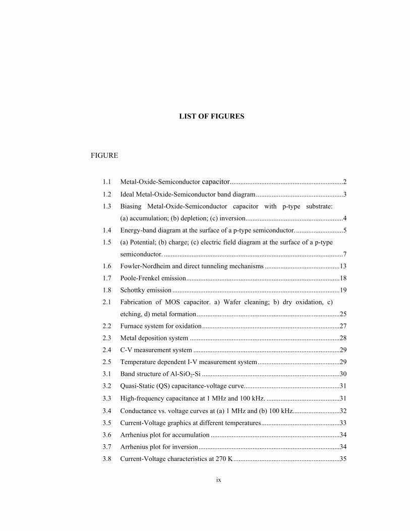
a) b) c)
Fig.1.3 Biasing Metal-Oxide-Semiconductor diode with p-type substrate: (a)
accumulation; (b) depletion; (c) inversion [1].
To understand the different bias modes of an MOS capacitor we now consider three
different bias voltages. These bias regimes are called the accumulation, depletion and
inversion mode of operation [3].
1.2.2.1 Accumulation
Accumulation occurs when one applies a voltage, which is less than the flatband voltage.
The minority carriers on the gate attract majority carriers from the substrate to the oxide-
semiconductor interface. Only a small amount of band bending is needed to build up the
accumulation charge so that almost all of the potential variation is within the oxide.
1.2.2.2 Depletion
As a more positive voltage than the flatband voltage is applied, a negative charge builds up
in the semiconductor. Initially this charge is due to the depletion of the semiconductor
starting from the oxide-semiconductor interface. The depletion layer width further increases
with increasing gate voltage.
1.2.2.3 Inversion
As the potential across the semiconductor increases beyond twice the bulk potential,
another type of negative charge emerges at the oxide-semiconductor interface: this charge
is due to minority carriers, which form a so-called inversion layer. As one further increases

5
the gate voltage, the depletion layer width barely increases further since the charge in the
inversion layer increases exponentially with the surface potential.
1.2.3 Surface Space-Charge Region
In this subsection, the relations between the surface potential, space charge and the electric
field are shown. These relations play important role in electrical characteristics of the ideal
MOS structures.
Figure 1.4 shows a detailed band diagram at the surface of a p-type semiconductor. The
potential ψs is defined as zero in the bulk of the semiconductor and is measured with
respect to the intrinsic Fermi level Ei as shown. At the semiconductor surface, ψ = ψs and ψs
is called the surface potential. The electron and hole concentrations as a function of ψ are
given by the following relations;
)exp()/exp(
)exp()/exp(
00
00
βψψ
βψψ
ppp
ppp
nkTqnn
pkTqpp
==
−=−= (1.2)
qФm
qФoxq χs
qVG
qФs = kT ψ(0) δp
Ei
EF
Fig.1.4 Energy-band diagram at the surface of a p-type semiconductor [1].

6
where ψ is positive when the band is bent downward (as shown in Fig.1.4), 0pn and
0pp
are the equilibrium densities of electrons and holes, respectively, in the bulk of the
semiconductor, k boltzmann constant, T temperature and β = q/kT. At the surface the
densities are:
)exp(pp
)exp(nn
spp
sps
0
0
βψ−=
βψ= (1.3)
From previous discussions and with the help of Eq.1.3, the following regions of surface
potential can be distinguished:
Ψs < 0 accumulation of holes (band bends downward)
Ψs = 0 flat-band condition
ΨB > Ψs > 0 depletion of holes (band bends downward)
ΨB = Ψs midgap with sn = sp = in (intrinsic concentration)
ΨB < Ψs inversion (band bends downward, electron enhancement)
The potential Ψ as a function of distance can be obtained by using the one dimensional
Poisson equation.
1.2.4. Work-Function Difference and Flat-band Voltage
For an ideal MOS diode, it is assumed that the work-function difference for an n-type
semiconductor is zero. If the value of фms is not zero and if oxide charges Q0 exist in SiO2,
the experimental capacitance-voltage curve will be shifted from the ideal theoretical curve
by an amount;
i
itmfoms
i
omsFB C
QQQQCQV +++
−φ=−φ= (1.4)
where VFB is called the flat-band voltage shift, Qf fixed charges, Qm mobile charges and Qit
interface states. If negligible interface traps, mobile ionic charges and oxide trapped
charges exist, equation reduces to;
i
fmsFB C
QV −φ= (1.5)

7
1.2.5 Ideal MOS Capacitor Analysis
We now give the MOS parameters with the aid of Figure 1.4
Fig.1.5 (a) Potential; (b) charge; (c) electric field diagram at the surface of a p-type
semiconductor [3].
Two assumptions will be made to simplify the MOS analysis: i) the full depletion
approximation can be used in a MOS-C and ii) inversion layer charge is zero below the
threshold voltage. We also assume that inversion layer charge linearly changes with the
gate voltage for voltages beyond the threshold. The derivation starts by examining the
charge per unit area in the depletion layer, Qd. As can be seen in Figure 1.5.b, this charge is
given by:
dad XqNQ −= (1.6)
Where Xd is the depletion layer width and Na is the acceptor density in the substrate. The
Electric field distribution which is obtained by integration of the charge density is shown in
Fig. 1.5.c. The electric field in the semiconductor at the interface, Es, and the field in the
oxide Eox, are equal:
s
das
XqNE
ε= (1.7)
The difference in the dielectric constants of oxide and semiconductor causes an abrupt
change in the electric field at the oxide-semiconductor interface. The dielectric constant for
Silicon is 11.9ε0 and for SiO2 is 3.9ε0. Therefore the electric field is about three times larger

8
in the oxide side at the semiconductor-oxide interface. The electric field in the
semiconductor changes linearly due to the constant doping density and is zero at the edge of
the depletion region. The potential shown in Figure 1.5.a is obtained by integrating the
electric field. The potential at the surface, ψs, equals:
2
2a d
ss
qN Xψε
= (1.8)
The calculated field and potential is only valid in depletion. In accumulation, there is no
depletion region and the full depletion approximation does not apply. In inversion, there is
an additional charge in the inversion layer, Qinv. This charge increases gradually as the gate
voltage is increased. However, this charge is only significant once the electron density at
the surface exceeds the hole density in the substrate, Na. We therefore define the threshold
voltage as the gate voltage for which the electron density at the surface equals Na. This
corresponds to the situation where the total potential across the surface equals twice the
bulk potential, ψB.
ln aB T
i
NVn
ψ = (1.9)
The depletion layer in depletion is therefore restricted to this potential range;
2 s sd
a
XqNε ψ
= for 0 2s Bψ ψ≤ ≤ (1.10)
For a surface potential larger than twice the bulk potential, the inversion layer charge
change increases exponentially with the surface potential. Consequently, an increased gate
voltage yields an increased voltage across the oxide while the surface potential remains
almost constant. We will therefore assume that the surface potential and the depletion layer
width at threshold equal those in inversion. The corresponding expressions for the depletion
layer charge at threshold, Qd,T, and the depletion layer width at threshold, Xd,T, are given as:
TdaTd XqNQ ., −= (1.11)

9
,2 (2 )s
d Ta
XqNε ψ
= (1.12)
Beyond threshold, the total charge in the semiconductor has to balance the charge on the
gate electrode, QM, or
)( invdM QQQ +−= (1.13)
where we define the charge in the inversion layer as a quantity which needs to determined
but should be consistent with our basic assumption. This leads to the following expression
for the gate voltage, VG:
d invMG FB s FB s
ox ox
Q QQV V VC C
ψ ψ += + + = + − (1.14)
where Cox is the oxide capacitance.
In depletion, the inversion layer charge is zero so that the gate voltage becomes:
2 s a sG FB s
ox
qNV V
Cε ψ
ψ= + + for 0 ≤ ψs ≤ 2ψB (1.15)
while in inversion this expression becomes:
4 s a s inv invG FB B T
ox ox ox
qN Q QV V VC C Cε ψ
ψ= + + − = ∆ − (1.16)
the third term in Eq.1.16 states our basic assumption, namely that any change in gate
voltage beyond the threshold requires a change of the inversion layer charge
1.3 MOS Capacitor and Oxide Charges
This section can be found in B. Van Zeghbroeck`s book, “Principles of Semiconductor
Devices” in a more detailed frorm [3]. The most important metal-insulator-semiconductor
structure is metal-SiO2-Si by far and in this subsection, SiO2-Si system will be described
briefly and the oxide and interface charges will be reviewed. A picture of the SiO2-Si

10
interface is that the chemical composition of the interfacial region, as a consequence of
thermal oxidation, is single-crystal silicon followed by a monolayer of SiOx, that is,
incompletely oxidized silicon, then a strained region of SiO2 and the remainder
stoichiometric, strain-free, amorphous SiO2. For a practical MOS diode, interface traps and
oxide charges exist that will, in one way or another, affect the ideal MOS characteristics.
There are four general types charges associated with SiO2-Si diodes :
i. Fixed Oxide Charge (Qf , Nf ); these are positive charges due primarily to structural
defects (ionized silicon) in the oxide layer. The density of this charge, whose origin
is related to the oxidation process, depends on the oxidation ambient and
temperature, cooling conditions, and silicon orientation. Because that the fixed
oxide charges cannot be determined unambiguously in the presence of moderate
densities of interface trapped charges, these are only measured after a low-
temperature hydrogen or forming gas anneal, which minimizes interface trapped
charge.
ii. Oxide trapped charges (Qot , Not ); these charges may be positive or negative due to
holes or electrons trapped in the bulk of the oxide. Trapping may result from
ionizing radiation, avalanche injection, tunneling or other mechanisms. Unlike
fixed oxide charges, oxide trapped charges are sometimes annealed by low-
temperature treatments, although neutral traps remain.
iii. Mobile oxide charges (Qm, Nm); these are caused primarily by ionic impurities such
as Na+, Li+, K+, and possibly H+. Negative ions and heavy metals may contribute to
this type of charges.
iv. Interface trapped charge (Qit, Qss, Nit, Nss Dit); this type of charge is also called
surface states, fast states, interface states, and so on. These are positive or negative
charges, due to structural defects, oxidation-induced defects, metal impurities, or
other defects caused by radiation or similar bond-breaking processes. These
charges are located at the SiO2-Si interface. Unlike fixed charges or trapped
charges, they are in electrical communication with the underlying silicon. Interface
traps can be charged or discharged, depending on the surface potential. Most of the
interface states can be neutralized by low-temperature hydrogen or forming gas
anneals. These localized states can affect the I-V characteristic of MOS capacitor.
The effect of these states can be grouped into two categories: The first group is
concerned with the electrostatic effects while the second with the dynamic effect
[2]. The electrostatic effect can be xplained as follows; due to the charge storage in

11
the surface states, charge distrubition through and voltage drop over the oxide are
affected strongly by interface state concentration Dit. There are two types of surface
states; donor-like and acceptor-like states. The energy of donor states is less than
the energy of surface state, which contributes a positive Qss when they are emptied
while the energy of the latter is greater than Ess which contributes a negative Qss,
when they are occupied. The value of Qss and its sign can increase or decrease the
band bending ψs. The dynamic effects of surface states are important at two points;
first, they provide additional path for the carriers and secondly, they act as
recombination centers.
1.4. Current Mechanisms in MOS Capacitors
In this section we present an extensive list of several proposed MIS current models and we
give brief descriptons of those models.
1.4.1 Fowler-Nordheim Tunneling
Fowler-Nordheim emission is one of the most important mechanisms in MOS structures. It
is the tunneling of electrons between the gate and the conduction band of the bulk through a
triangular barrier. This mechanism was first proposed by Fowler and Nordheim [5] and
then named after them. In the last three decades the FN tunnelng in the MOS capacitor
structure has been intensively studied by many researchers [6-18]. The tunnel current
component is computed as;
)/exp(|| 2 EbEaJ FN −= (1.17)
where a and b are fitting parameters and E is the electric field in the oxide. Lenzlinger and
Snow [6] generalized the model and obtained a more explicit analytical result. Their current
density is given as:
)324
exp(8
320
3
Eqm
Ehmmq
J box
boxFN
φπφ
−⋅= (1.18)
where mox is the mass of the carriers in the oxide, m0 is the free electron mass, h planck
constant, q charge and φ is the potential barrier height that a carrier tunnels through. The
oxide mass and the barrier height are used as physically-based fitting parameters. This

12
emission occurs under high electric field (more than 8-10 MeV/cm) since the theory
assumes the barrier to be triangular. A brief derivation of Fowler-Nordheim current density
for simple case ,that is no image force lowering or no finite temperature effects, is as
follows (in this derivation we follow Depas et. al. [19]):
The tunneling current between tha gate and the semiconductor is given by
∫∫=E
tt
Et
FN dETdEhqm
JF
003
4π (1.19)
where Et is the transversal energy component, E the energy of the tunneling electron
measured from the semiconductor conduction band edge at the SiO2-Si interface and Tt the
tunneling probability. Tt is given by WKB approximation as:
))(2exp(1
0∫−=x
oxt dxxkT (1.20)
where kox is the wave vector of the tunneling electron and x is the barrier length. After all
the calculations performed, the tunneling probability is found as;
))(
324
exp(
2/3
ox
ox
ttFb
oxt E
mEm
EE
qhm
T+−+
−=φ
(1.21)
A first order Taylor expansion on T around E = EF and Et = 0 leads to the Eq.1.18. A plot of
ln (J/E2) vs. 1/E ,so called Fowler-Nordheim plot, should be straight line if the F-N
mechanism is the dominant mechanism in conduction through the oxide. The intercept and
the slope of this plot yield the oxide mass and the barrier height.
1.4.2 Direct Tunneling
An accurate modeling of tunneling current in today`s ultra-thin oxide MOS devices cannot
be accomplished by widely used Lenzlinger-Snow FN model since it implies a metal as a
gate and a triangular barrier. They are largely obsolete conditions for today`s devices where
very high tunneling probability due to ultra-thin oxides (less than 4-5 nm), quantization
effects of both electrons and holes in both inversion and accumulation regime, poly-silicon

13
depletion, several tunneling mechanisms besides conduction band electron tunneling and a
trapezoidal barrier play fundamental role in conduction. For these reasons many authors
have proposed new models to introduce these effects into current modeling [20-27]. In
1993, Schuegraf and Hu [28] introduced a tunneling model by taking the fact that the poly-
silicon gate and interface states at SiO2-Si cause a trapezoidal barrier rather than triangular
barrier as in Fowler-Nordheim emission, into account. Their approach was the same as
Snow and Lenzlinger`s but their tunneling probability was modified approprietly with
respect to new barrier shape:
Fowler-Nordheim tunneling
Direct tunneling
Metal Oxide Semiconductor
Fig. 1.6. Fowler-Nordheim and direct tunneling mechanisms.
The tunneling probability is given as:
))()(
324
exp(
2/32/3
ox
oxox
ttFb
ox
ttFb
oxt E
qVm
EmEE
mEm
EE
qhm
T−+−+−+−+
−=φφ
(1.22)

14
They computed the current density as:
( ) [ ]
−−
⋅−−⋅
−−−−−
⋅= )/11(
23exp(1)/1(1exp
/112/3
2
2
boxbox
Fbox
oxbox
DTt qVEBEqV
EB
qV
EAJ φ
φφ
φ (1.23)
with A and B, defined as:
b
oxo
hmmq
Aφπ8
)/(3
= and qhm
B box
328 3φπ
= (1.24)
For accumulation case, where
ox
bF qBt
E3
4 3φ> (1.25)
the current density reduces to;
( ) [ ] ⋅
−−−−−
= 2/32
2
)/1(1exp/11
boxoxbox
DTt qVEB
qV
EAJ φ
φ (1.26)
In 2000, Lee and Hu [29], proposed a generalized direct tunneling model which is valid in
both depletion and accumulation. The current density in their model is very similar to
Schuegraf-Hu model except for the correction function;
[ ]
−−−⋅= 2/33
)/1(1exp),,,(8 box
oxboxoxG
boxDTt qV
EBtVVC
hqJ φφ
φεπ (1.27)
where C(VG, Vox, tox, фb) is the correction function;
NtVVV
tVVCox
G
b
ox
off
box
bboxoxG ⋅⋅
−⋅+
−−= )1()1(20exp),,,(
φφφ
φφ α (1.28)
−−+⋅+
−+⋅⋅= )exp(1ln)exp(1ln
T
FBGT
Tinv
Teff
ox
ox
VVV
VVn
VVS
tN
ε (1.29)

15
where α is a fitting parameter, tox is the tickness of the oxide, S is subtreshold swing, VT is
the thermal velocity.
The main difference between this model and Schuegraf`s model is the correction factor.
The exponential term accounts for secondary effects such as energy dependence of the
densities of states at the electrode interface and effective masses in the dielectric, and that
affects the curvature of the tunneling characteristic. N is an indicator of the density of either
the tunneling carriers for electron conduction band tunneling (ECB) and hole valence band
tunneling (HVB) or the receiving energy states for EVB. The rate of increase of the
subtreshold carrier density with VG is dictated by n=S/VT (S is the subtreshold swing in
inversion or accumulation). These effects were neglected in Schuegraf`s approach altough
that approach gives good results in accumulation and depletion modes.
There are also many other direct tunneling models proposed by different groups as brand
new models or modification of Schuegraf-Hu model [29-48].
1.4.3 Band-to-Band Tunneling
This model describes the current due to carriers tunneling between the band of the
semiconductor to the band of the gate and vice versa. It describes the same physicsal
process with Fowler-Nordheim and Direct tunneling do. The difference between this model
and Fowler-Nordheim or Direct Tunneling model is the temperarture dependency. The
difference comes from the handling of the systems. This model follows the same steps
while deriving the final current density function but it uses the thermal velocity. This
approach causes a second order temperature factor in the final form of current density. The
derivation can be summarized as follows and the details can be found in Card-Rhoderick
[49, 50]or Kumar-Dahlke [51]:
Starting from the Eq.1.19 and substituting the tunneling probability into that equation and
evaluation of the integration over the energy range yields;
[ ]1)/exp()/exp()exp(2* −⋅−⋅−⋅= kTqVkTqTAJ GsbBTB φβφ (1.30)
where A* is the Richardson constant, exp(-βфb) the tunneling probability, φs the schottky
barrier between the gate and the semiconductor. There is a significant similarity between
this model and Schottky theory since the kinetic energy of the carriers is used in transport
equations. In other words band-to-band tunneling can be approximated as Schottky model

16
with a transmission probability through the oxide and this mechanism can be important for
especially MOS diodes with very thin (~ 5-10 Angstrom) oxide.
1.4.4 Trap Assisted Tunneling
There are many models related with traps such as pure trap assisted tunnelings or Poole-
Frenkel emission or hopping conduction etc. In this subsection, hovewer, we only present
the pure trap assisted tunneling models in the oxide. The other mechanisms mentioned
above will be given in subsequent sections.
The existance of electron trap levels in the dielectric layer of a metal-oxide-semicondcutor
device can result in a considerable leakage current at electric fields well blow those needed
for Fowler-Nordheim or direct tunneling, in which electrons gain sufficient energy to tunnel
directly from the gate electrode to the inulator or semiconductor conduction band and vice
versa. Trap assisted conduction is a two-step process in which electrons first tunnel directly
into a trap, and then are able to tunnel into the conduction band of the insulator or
semicondcutor, incorporating energy loss by phonon relaxation.
The electrical conduction mechanisms of thin trapped oxides and nitrides have attracted
much attention over many years [52-67]. The basic trap assisted current density is given as;
∫ +=
oxt
o
ttTAT PP
PPNCqJ
21
21 or ∫ +=
oxt
ec
tTAT dx
qNJ
0 ττ or ∫ +
=oxt
outin
outintTAT dx
JJJJ
NJ0
σ (1.31)
or in similar forms. However the models employed in the form above work rely on the
calculation and numeraical evaluation of integrals and hence are not readily applied to
experimental data. There are also other TAT tunneling models that are ready to be applied
to experimental data. We give a small description of those models in subsequent
subsections.
Fleischer`s TAT Model;
In 1992 Fleischer, Lai, and Cheng [55] proposed a trap assisted tuneling model in MOS
devices. Their model is based on two-step tunneling. The current density is given as in
Eq.1.31. This equation reduces to

17
EE
AENqC
Jttt
TAT 3
)exp(3
2 2/3φφ−⋅
= (1.32)
This equation makes it possible to extract the trap energy from the slope of the plot of ln
(JE) vs. 1/E without heavy calculations;
3/2)(A
slopet −=φ (1.33)
The advantage of these appraoches is the easiness of data evaluation and reduced number of
fit parameters. One doesn`t need to make simulations or heavy computational calculations.
Instead, by plotting ln (JE) vs 1/E, it i easy to determine the trap energy from the slope. By
deriving trap energy as a first step, the fitting procedure can be expected to be easier and
more accurate. It is necessary to either use both φt and Nt as fitting parameters or to
determine one of them by an independent method (such as C-V, avalanche injection, high-
field injection or Poole-Frenkel evaluation etc.) when the numerical solution or simulation
tools are used. Now both of these trap parameters can be extracted directly from the I-V
measurements with respect to this theory.
Chang`s TAT Model;
This model [65] employs a general trapezoidal barrier rather than a triangular barrier which
is oftenly used in conventional trap assisted models. The derivation of an explicit analytical
current density is the same as in Fleischer`s model except the barrier function. The model
predicts the current density as:
)3
24exp(
2/3
Eqm
J oxTAT
φ−∝ (1.34)
By plotting ln(J) vs 1/E, it is easy to determine the trap energy from the slope.
1.4.5. Poole-Frenkel Tunneling
This mechanism is due to field-enhanced thermal excitation of trapped electrons into the
conduction band of SiO2. The structural defects cause additional energy states close to the
band-edge called traps. These traps restrict the current flow because of a capture and
emission process. The current is a simple drift current described by

18
EnqJ PF µ= (1.35)
where n is the carrier density and µ mobility [67]. While the carrier density depends
exponentially on the depth of the trap which is corrected for the electric field
−−=
it
qEkTqnn
πεφexp0 (1.36)
then current density becomes;
−−⋅=
itPF
qEkTqEqnJ
πεφµ exp0 (1.37)
Metal Oxide Semiconductor
qФPF
Fig. 1.7 Poole-Frenkel emission
1.4.6. Space-charge limited current
The space-charge limited current results from carrier injection into the insulator, where no
compensating charge is present. For structures where carriers can readily enter the insulator
and freely flow through the insulator one finds that the resulting current and carrier
densities are much higher. The density of free carriers causes a field gradient, which limits
the current density. This situation occurs in lowly doped semiconductors and vacuum tubes.
19
The well-known expression for space charge limited current, Eq. 1.38, is found by starting
from an expression for the drift current and Gauss's law (it is assumed that the insulator
contains no free carriers if no current flows). See for example [3] for details.
3
2
89
dVJ ⋅⋅
=µε
(1.38)
where d is the thickness, ε is the permittivity and µ is the mobility of the insulator.
1.4.7. Hopping Conduction (Ohmic Conduction)
At very low voltages and high temperatures, current is expected to be carried by thermally
excited electrons hopping from one isolated state to the next. This mechanism yield an
ohmic characteristic exponentially dependent on temperature. The current density is given
as [1]:
)/exp( kTEEJ a∆−⋅∝ (1.39)
where ∆Ea is the activation energy.
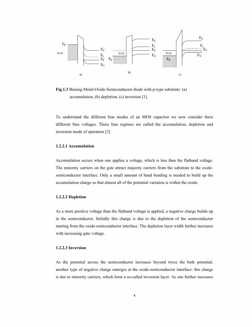
1.4.8. Schottky-like Emission (Modified Poole-Frenkel Current)
This mechanism is similar to the thermionic emission in metal-semiconductor junctions.
Thermal electrons which are emitted across the gate-oxide or semicondcutor-oxide
interface are responsible for the carrier transport.
Metal Oxide Semiconductor
qФB
Fig. 1.8 Schottky emission

20
The thermionic emission theory by Bethe [68] is derived from the assumption that (i) the
barrier height is much larger than kT and (ii) thermal equilibrium is established at the plane
that determines emission, and (iii) the existance of net carrier flow does not affect this
equilibrium. Because of these assumptions the shape of the barrier profile is immaterial and
the current flow depends solely on the barrier height. The current density between the gate
and the semiconductor is then given by the concentration of electrons with energies
sufficient to overcome the potential barrier and traversing in the transport direction:
∫∞
+
=BqFE x dnqvJ
φ (1.40)
where EF + qΦB is the minimum energy required for thermionic emisson into the oxide, and
vx is the carrier velocity in the direction of transport. The electron density in an incremental
energy range is given by :
( ) ( )[ ]dEkTqVEEEEhmdEEFENdn ncc /exp24)()( 3
2/3
+−−−==∗π
(1.41)
where N(E) and F(E) are the density of states and the distribution function respectively and
qVn is (Ec-EF). If we postulate that all the energy of electrons is kinetic energy, then
2
21 vmEE c
∗=− (1.42)
If the speed is resolved into its component along the axes with th x axis parallel to the
transport direction, we have
2222zyx vvvv ++= (1.43)
With the required transformations, we obtain the thermionic current as;
( )
−−=
∗∗
kTvm
kTqVTAJ oxn 2
exp/exp2
2 (1.44)

21
where vox is the minimum velocity required in the x direction to surmount the barrier and is
given by
)(21 2 VVqvm biox −=∗ (1.45)
where Vbi is the built-in potential at zero bias. Substituting Eq.1.45 into Eq.1.44 yields
( )
−= ∗
kTqVkTqTAJ B exp/exp2 φ (1.46)
Since the barrier height for electrons moving into the oxide remains the same, the current
flowing into the oxide is thus unaffected by the applied voltage. It must therefore be equal
to the current flowing from the semiconductor into the metal when thermal equilibrium
prevails (i.e. when V=0). The corresponding current density is obtained from Eq.1.46 by
setting V=0 as;
( )kTqTAJ B /exp2 φ−= ∗ (1.47)
However, when the electron enters the oxide, charge is redistributed on the electrode to
maintain the equipotential surfaces. The result is to produce a so-called image field that
adds to the applied field and helps to round and lower the potential barrier. The image
lowering is given as [1] :
πε4qE (1.48)
and the thermionic current for MOS devices becomes
−= ∗ kTqEqTAJ b /
4exp2
πεφ (1.49)
A plot of ln(J/T2) vs. 1/T yields a straight line with a slope determined by the permittivity
of the oxide.

22
1.4.9. Surface-State Tunneling
Following the approach of Freeman and Dahlke [69, 70], the electron current, Jns, from the
conduction band of the semiconductor to the surface states is given by:
))1[( 1nfnfvqDJ tstnthitns −−= σ (1.50)
where νth is the thermal velocity, Dit density of surface states, σ capturre cross-section area
for electrons, ƒt surface state occupation probability with tunneling current through the
surface states, ns (ps) electron (hole) concentration at the semiconductor surface, n1 (p1)
electron (hole) concentration if the electron (hole) Fermi level is at the trap energy level.
The hole current, Jps, from the valence band to the surface states can be written as:
])1([ 1pfpfvqDJ tstpthitps −−= σ (1.51)
and the total current through the surface states, Jss ,is
)( mtt
itpsnsss ff
qDJJJ −=−=
τ (1.52)
where ƒm is the occupation probability of an energy level in the metal. By substituting the
Eqn.1.50 and Eq.1.51 into Eq.1.52 one obtains the surface state tunneling density. See [45]
for details. Surface states provide additional path for carriers and they act as recombination
centers at the surface.
1.4.10. Diffusion Current
Diffusion current can be calculated by following Hovel`s approach [71] by solving the
continuity equation and applying the appropriate boundary conditions. Diffusion current
can behave a limiting current when all the carriers supplied to the substrate are able to pass
to the gate. This mechanism can especially be important in thin oxides where the
transmission probability through the oxide is very high and the current in the device will be
governed by the substrate. Mathematical details can be found in many papers [70].

23
1.4.11. Recombination-Generation Current
The generation-recombination mechanism plays an important role in MOS devices due to
oxide-semiconductor interface. The surface states can behave as a recombination centers. If
the surface state density is high then recombination-generation current might be significant
and descriptive for a MOS device. The recombination-generation current is given as:
)1( 2/ −= sewqn
Jn
irg
βφ
τ (1.53)
The derivation of this formula can be found in many books [1].

24
CHAPTER 2
EXPERIMENTAL PROCEDURES
We will briefly describe the basic fabrication steps of MOS capacitors. This chapter does
not aim to explain all the process methods and details of a MOS capacitor but only main
steps of fabrication of our samples. We will also give a short description of our
measurement setup for current-voltage measurements.
One of the samples (Aliminum gate MOS) was prepared at our laboratory, and the other
sample (PolySi gate MOS) was prepared at Physical Electronics & Photonics Laboratory at
Chalmers, Sweden.
2.1 Al-SiO2-Si MOS
The first sample we worked on was a relatively thick oxide MOS capacitor (1250
Angstroms) with Al/SiO2/n-Si structure. To produce this sample we basically followed the
steps shown in the figure 2.1 below:
Our wafer was n-type Si (100) with a doping of 1x10¹⁶. We applied a cleaning procedure to
this wafer to reduce the contamination on the wafer (Fig.2.1.a). Then we used thermal
oxidation (dry) method under N2 atmosphere to coat the Si with SiO2 (Fig.2.1.b). The
oxidation was performed in a furnace at 1050 0C for 80 minutes. In this phase of the
process, top and bottom surface of the Si-wafer was coated with SiO2. Then, the bottom
oxide was etched with Hydrofluoric acid (HF, 10%) to be able to deposit metal (Al) onto Si
for back contact (Fig.2.1.c). After etching, we formed the gate of our MOS-C by Aluminum
deposition with the help of a shadow mask in a deposition chamber. Finally, we deposited
Aluminum onto the back side of the Si-wafer to have the back contact (Fig.2.1.d).
We will present the Si-wafer cleaning procedure in detail and abrief summary of oxidation
in In subsection 2.1.1. and 2.1.2.

25
..
Figure.2.1. Fabrication of a MOS capacitor: a) Wafer cleaning; b) dry oxidation, c)
etching; d) Metal formation.
2.1.1 Wafer Cleaning
Wafer cleaning has a central role in semiconductor device production. Due to the fact that
existing organic (dust, oil etc.) and inorganic (native oxide, metallic ions etc.)
contaminations on the wafer can effect the characteristics of the devices, wafers must be
cleaned before any processing.
The first sample we used in this study was cleaned before oxidation with the following
chemical processes:
1. Boiling in trichloroethylene: Removes organic contaminants,
2. Ultrasonically agitation first in deionized water and later in acetone,
3. Boiling in the mixture of HCl : H2O2 : H2O : Removes metallic impurities and
prevents their displacement plating back onto the silicon,
4. Washing in deionized water for a few minutes: Cleans up the traces of the
chemicals from the preceding treatment,

26
5. Boiling in the mixture of H2SO4 : H2O2 : H2O : Removes both organic and metallic
films,
6. Washing in deionized water : Removes the remnants coming from the previous
step,
7. Dipping a solution of HF: H2O: Strips the thin native oxide layer on the sample
(silicon atoms bond with the hydrogen atoms after the removing of oxide on the
surface and this prevents the wafer from new oxidation for a while).
8. Washing in deionized water,
9. Drying by using N2.
2.1.2 Oxidation
An oxide layer is rapidly formed when silicon wafer is exposed to an oxidizing ambient
since silicon surface has a high affinity for oxygen. Two techniques are commonly used for
oxidation: Thermal oxidation and chemical vapor deposition (CVD).
The deposition of SiO2 using a CVD process is one where two gases, silane and oxygen,
react to form silicon dioxide, which then sublimes onto any solid surface. The wafers are
heated to 200 - 400°C yielding high quality oxides.
The thermal oxidation of silicon is obtained by heating the wafer in an oxygen or water
vapor ambient. Typical temperatures range from 800 to 1200°C. The oxidation of a silicon
surface also occurs at room temperature but the resulting 3 nm layer of oxide limits any
further oxidation. At high temperatures, oxygen or water molecules can diffuse through the
oxide so that further oxidation takes place. The oxidation in oxygen ambient is called a dry
oxidation. The one in water vapor is a wet oxidation. The thermal oxidation provides a high
quality interface and oxide. It is used less these days because of the high process
temperatures [3].
Finally Aluminum deposition process was performed for front and back contacts. Fig. 2.3
below shows our metallization setup.

27
Quartz boat Quartz tube
Furnace
Filter
N2 O2
Temperaturecontroller
Fig. 2.2 Furnace system for oxidation
2.2. PolySi-SiO2-Si MOS
This sample was prepared at Physical Electronics and Photonics Laboratory of Chalmers
University of Technology, Gothenburg, Sweden. The structure is p-polysilicon/SiO2/n-Si.
The details are as follows:
The capacitor (PMOS) was fabricated on (100) n-type Silicon wafers from Wacker
Silctronic. Ultrathin nitrided gate dielectric structure was grown at 750-800 0C by using an
ASM A400 vertical furnace. The gate electrode p+-poly-Si (p-type, Boron doped greater
than 1x1020 cm-3 and its thickness is 200 nm) was deposited in a low pressure chemical
vapor deposition (LPCVD) ASM chamber using SiH4 at a pressure of 5.3x10³ pa and
temperature of 615 0C. In order to facilitate nucleation of poly-Si on the SiO2 an undoped Si
seed layer with a nominal thickness of 1 nm was deposited at 615 0C prior to poly-Si layer
deposition [3].

28
pyrex bell-jar
holder
shuttermolybdenum boat
filament current
base plate
cooling and pressure systems,pumps, gauges and valves.
Fig. 2.3 Metal deposition system
2.3. Electrical Characterization Setup
In this thesis two different electrical measurements were performed; current-voltage (I-V)
and capacitance-voltage (C-V). The aim of this thesis is to investigate the electrical
transport in MOS structures based on I-V methods. Therefore C-V investigation is out of
the scope of this thesis and will not be discussed in detail in this thesis, but we will give the
basic C-V curves of our samples for the sake of completeness of electrical characterization.
Only I-V measurements were performed as temperature dependent due to the same reason
and C-V measurements were performed at 300 0K.
We used Hewlett- Packard (HP) 4140B pA meter / DC voltage source for I-V measurement
and HP 4192 LF impedance analyzer for C-V measurements. Basic schematics of these
setups are as follows:

29
Fig.2.4 C-V measurement system.
Figure 2.5 Temperature dependent I-V measurement system.

30
CHAPTER 3
ELECTRICAL TRANSPORT IN THICK SIO2 FILM
3.1. Al-SiO2-Si Capacitor
In this part of the thesis, we present our work on MOS capacitor fabricated on a thick SiO2
layer. The oxide thickness is 1250 ±10 Angstroms. The gate material is Aluminum and the
substrate is n-type Silicon (100). Fabrication processes were described in the previous
chapter. The band diagram of this structure is as follows:
Fig. 3.1 Band structure of Al-SiO2-Si

31
3.2. Electrical Characteristics:
3.2.1. C-V and G-V Curves:
The C-V curves of the sample are as follows:
-5 -4 -3 -2 -1 0 1
2.0x10⁻¹⁰
4.0x10⁻¹⁰
6.0x10⁻¹⁰
Cap
acita
nce
(QS
)
Voltage
Fig. 3.2 Quasi-Static (QS) capacitance-voltage curve of sample-1
-6 -4 -2 0 2 4 60.0
5.0x10⁻¹¹
1.0x10⁻¹⁰
1.5x10⁻¹⁰
2.0x10⁻¹⁰
2.5x10⁻¹⁰
3.0x10⁻¹⁰
3.5x10⁻¹⁰
4.0x10⁻¹⁰
Cap
acita
ne (H
F)
Voltage
1 Mhz 100 khz
Fig.3.3 High-frequency capacitance at 1 MHz and 100 kHz.
32
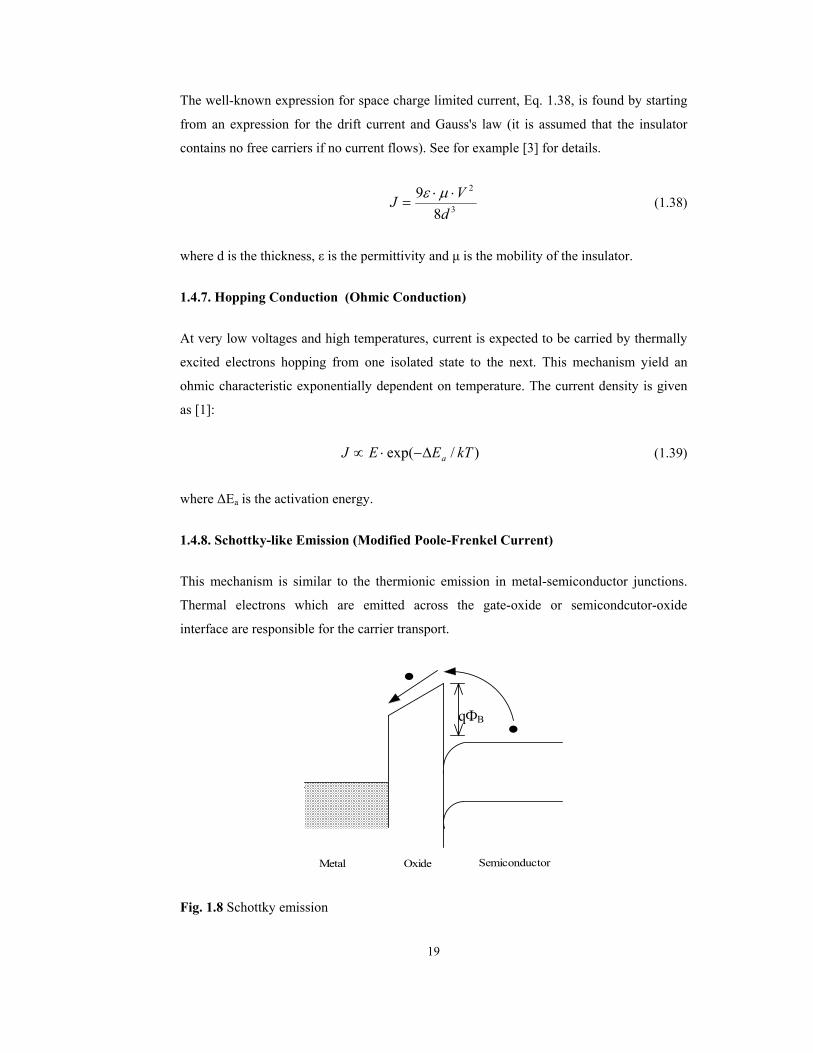
Fig. 3.4 shows the conductance-voltage curves we measured at the same frequancies:
-6 -4 -2 0 2 4 6
0.0
1.0x10⁻⁴
2.0x10⁻⁴
3.0x10⁻⁴
4.0x10⁻⁴
5.0x10⁻⁴
6.0x10⁻⁴
7.0x10⁻⁴
8.0x10⁻⁴
Con
duct
ance
(G)
V o ltage
(a)
(b)
Fig.3.4 Conductance vs. voltage curves at (a) 1 MHz and (b) 100 kHz.
The quasi-static and high frequency curves indicate a certain MOS structure but they also
show a leakage current in the oxide. The conductance-voltage curve shows a minimum at
almost V=0. G-V curve also reveals that there is a leakage in the accumulation regime. This
means that the carriers are able to pass through the oxide and the conductance increases due
to these carriers. However, the saturation in the high frequency capacitance in accumulation
indicates that the ratio of the leakage carriers is small compared to total carriers.
A thick oxide contains traps and these traps help carriers to leak in the oxide. Flat band
voltage value (~-2.3 V) also supports these basic conclusions about our oxide.
3.2.2. I-V Curves
Current-Voltage measurements were performed in a broad temperature range from 20 K to
300 K. The I-V curves at selected temperatures are shown in figure 3.5:

33
-4 -2 0 2 4 610-8
10-7
10-6
10-5
10-4
Cur
rent
(A)
Voltage (V)
300k 250k 150k 200k 100k
Fig. 3.5 Current-Voltage graphics at different temperatures.
In the accumulation regime, an explicit temperature dependence can easily be observed.
Also a series resistance effect is seen in the figure 3.5, after about 1 volts at all
temperatures. In the inversion, however, a weaker dependence on temperature is seen in the
figure above. To find out which current mechanisms are responsible for this kind of
behavior, we plotted the Arrhenius plots for both positive and negative voltage regimes.
3.3. Possible Current Transport Mechanisms:
We observed mainly two different characteristics in the Arrhenius plots for accumulation.
As seen in Fig. 3.6, there is a strong temperature dependence at high temperatures. We
observe a field activated process at medium and low temperatures. The same observation
can easily be done by studying the I-V curve, shown in Fig. 3.5. One can easily realize that
the current does not change significantly with the temperature (100 K and 200 K). At
higher temperatures, an explicit increase in current is observed as the temperature increases
(250 K and 300 K). The dependence on temperature also shows differences at different
fields.

34
0 5 10 15 20 25 30 35
10-6
10-5
Cur
rent
(A)
1000/T (K-1)
0.6V 1.6V 2.6V 3.6V
Fig. 3.6 Arrhenius plot for accumulation
5 10 15 20 25 30 3510-7
10-6
10-5
Cur
rent
(A)
1000/T (1/K)
-0.6 V - 1 V - 2 V - 3 V
Fig. 3.7 Arrhenius plot for inversion

35
In the inversion regime, Arrhenius plot shows two different behaviors as a function of
temperature and field, but in a different way than the Arrhenius plot for accumulation does.
The temperature dependence is only seen at higher fields and at low fields we see a noisy
data. At high fields, for example -3 V or -2 V, the current depends exponentially on
temperature. The weak temperature dependence of the current at -1 V and temperature
independence at lower fields suggest the existence of another mechanism.
As we presented in the first chapter, there are mainly four conduction mechanisms which
are temperature dependent. These mechanisms are Schottky emission, band-to-band
tunneling, Poole-Frenkel emission and ohmic conduction.
We plotted Poole-Frenkel curves at various temperatures and calculated the permittivity
from those plots. We did this procedure for 270 K at first and then for all temperatures
since we expect the Poole-Frenkel conduction to occur at higher temperatures: In the next
section we will present the I-V and Poole-Frenkel plots [ln (J/E) vs. E1/2] for accumulation
and inversion at 270 K.
3.3.1. Thermally Activated Current
-4 -3 -2 -1 0 1 2 3 4 5 6 7 8
10-7
10-6
10-5
10-4
I (A
)
V (volt)
I-V plot 270 K
Fig. 3.8 Current-Voltage characteristics at 270 K.

36
In the Fig. 3.5 and Fig. 3.8, we can see that series resistance affects the current-voltage
characteristics of the device at voltages higher than approximately 1.5 V in accumulation
regime. For this reason, we expect Poole-Frenkel curves to give good results below this
threshold.
-1x10² -2x10² -3x10² -4x10² -5x10² -6x10²
1E-11
1E-10
1E-9
J/E
sqrt(E)
Fig. 3.9 Poole-Frenkel plot at 270 K for inversion.
In Fig. 3.9, Poole-Frenkel curve obtained from the experimental data at 270 K (circles) and
two linear fits (black lines) to the curve are shown. Since the slope of Poole-Frenkel plot
gives a function of temperature and permittivity, extracting the value of the permittivity
from the slope is a simple algebraic procedure.
The Poole-Frenkel current density expression is given as:
−−⋅=
itPF
qEkTqEqnJ
πεφµ exp0 (1.37)
And the slope of the Poole-Frenkel curve is:
i
qkTqslope
πε−= (3.1)

37
where q is the electron charge, k is Boltzmann constant, T is temperature and εi is the
permittivity of the oxide.
One of the slopes (the upper one) in the Fig. 3.9 produced the permittivity as 0.85 ε0 where
ε0 is the vacuum permittivity. The permittivity was found as 9.8 ε0 for the other fit to the
slope. It is clear that a better fit, which might give a permittivity value close to the
commonly accepted 3.9 ε0 value, can be found by making a fit between these two lines. The
trap depth changes between 0.69 eV and 0.75 eV with respect to these permittivity values.
These two results when they are considered with the discussion above lead to the
conclusion that the transport mechanism of the device is dominated by the Poole-Frenkel
conduction at 270 K for inversion. Actually one does not have to extract perfect
permittivity values from Poole-Frenkel plots since oxides include a lot of deficiencies such
as oxide traps, mobile ions, localizations in the matrix an so on. These imperfections cause
permittivity deflect from 3.9 ε0. Therefore values found in the above analysis are good signs
to assure us about the dominance of the Poole-Frenkel emission.
Therefore our conclusion for the conductivity in the device for inversion regime is Poole-
Frenkel type trap assisted conduction. In order to be sure of this conclusion we plotted
Poole-Frenkel curves at other temperatures. The results and the fits to the slopes of those
curves are shown in figure 3.10 below:
-1x10² -2x10² -3x10² -4x10² -5x10² -6x10²
1E-11
1E-10
J/E
E1/2
100 K 150 K 200 K 250 K 300 K
Fig. 3.10 Inversion regime Poole-Frenkel graphics at various temperatures.

38
The permittivity values extracted from these slopes are acceptable for high temperatures.
For example at 300 K, the permittivity was found as 6.8 ε0 and this value goes away from
3.9 ε0 as the temperature decreases. This increase in permittivity values indicates that the
second conduction mechanism, which was mentioned during the Arrhenius plot discussion
above, becomes more effective at lower temperatures. The trap depths change from 0.56 eV
to 0.60 eV. Trap depth decreases as the temperature increases. This is expected since as the
temperature increases carriers will have more average energy and therefore they will be
able to jump to higher trap states.
The Poole-Frenkel curve yielded a 6.49 ε0 value for the accumulation regime. The Poole-
Frenkel curve and the fit to the linear region of the curve are shown in Fig.3.11:
0.0 2.0x10³ 4.0x10³ 6.0x10³
1E-12
J/E
E1/2
Fig. 3.11 Poole-Frenkel plot at 270 K for accumulation.
The permittivity value was found to be 6.49 ε0 from the slope of the fit. This value is
convincing enough to reach to the conclusion that Poole-Frenkel conduction governs the
device at 270 K. The trap depth of 0.67 eV corresponds to 6.49 ε0.
The Poole-Frenkel plots for other temperatures are shown in Fig. 3.12 below. From the
slopes of the fits seen in the figure 3.12, we extracted different permittivity values as 5.5 ε0

39
for 300 K, 13.2 ε0 for 200 K and 262.5 ε0 for 100 K. It is seen that the permittivity values
become less and less acceptable as the temperature decreases. This behavior again indicates
the two-component conduction we described before. As the temperature decreases Poole-
Frenkel conduction loses its dominance and the other mechanism starts to show up more.
The trap depth for 250 K was found as 0.51 eV. The trap depth decreases as the temperature
increases again. Unlike the inversion regime in which traps show minor differences in
depth (0.56 eV to 0.60 eV), the trap depth changes more significantly in
accumulation. It is 0.51 eV for 250 K and 0.67 eV for 270 K. This drastic change in
accumulation is understandable since a change in the conduction mechanism occurs
at these temperatures. Current becomes dominated by Poole-Frenkel emission rather
than the field activation.
1x10² 2x10² 3x10² 4x10² 5x10² 6x10² 7x10² 8x10² 9x10²
10-10
J/E
X Axis Title
J100K J150K J200K J300K J250K
Fig. 3.12 Accumulation regime Poole-Frenkel graphics at various temperatures.
Up to now temperature dependent component of the total current has been discussed in
detail and the field activated component was mentioned several times. We will discuss the

40
field activated constituent of the total device current in the next section.
3.3.2. Field Activated Current:
There are different current models related to field activation. For example Fowler-
Nordheim emission, direct tunneling, trap assisted tunneling, space-charge limited current,
diffusion current, recombination generation current and surface state tunneling. However
most of these models are not applicable to our device since it contains a relatively thick
oxide about 1250 Angstroms. This oxide is very thick for substrate currents to limit the
total current in the device. Such a thing only happens when all the carriers injected to
substrate pass to the gate. And the device must be ready for new more carriers. It is obvious
that our oxide is too thick by far for such a thing. Surface state tunneling and
recombination-generation models do not work due to the same reason. It is also commonly
accepted that direct tunneling occurs in 4-5 nm oxides and Fowler-Nordheim tunneling is
not expected to be seen before 9-10 MV/cm fields. The field we applied is much less than
this value. The most appropriate model seems to be trap assisted tunneling in this case.
There are mainly two approaches to trap assisted tunneling: Numerical models and
analytical solutions. The trap assisted tunneling is given as:
∫ +=
oxt
o
ttTAT PP
PPNCqJ
21
21 (1.31)
or
∫ +=
oxt
ec
tTAT dx
qNJ
0 ττ (1.31)
where tox is the oxide thickness, Ct is a slowly varying function of electron energy, Nt is the
trap density, P1 and P2 are the electron tunneling probabilities and τc and τe are the caption
and emission times of the traps.
One needs several physical quantities such as life times, trap depths or trap distributions to
evaluate these integrals. However, these parameters can be found by other characterization
methods than current-voltage analysis. This is however outside the scope of this thesis.

41
The analytical approaches have been developed to investigate the pure trap assisted
conduction by using the I-V data by different researchers. There are mainly two methods by
Fleisher-Lai and Chang et. al. [55, 65].
These two methods are very similar to each other although Chang’s method is more
generalized. Fleischer-Lai (4.5) and Chang (4.6) models are formulated as:
EE
AENqC
Jttt
TAT 3
)exp(3
2 2/3φφ−⋅
= (1.32)
)3
24exp(
2/3
Eqm
J oxTAT
φ−∝ (1.34)
where Φt is the trap depth.
One has to plot ln (J•E) vs. 1/E in Fleischer-Lai model and ln J vs. 1/E in Chang`s model.
Both plots give a slope of (-AΦt3/2) where A=4(2qm*)1/2/3ћ.
0.0 1.0x10⁻⁷ 2.0x10⁻⁷ 3.0x10⁻⁷ 4.0x10⁻⁷ 5.0x10⁻⁷ 6.0x10⁻⁷ 7.0x10-7100
101
102
103
J*E
1/E
200 K 150 K 100 K 250 K 300 K
Fig. 3.13 Fleischer-Lai trap assisted tunneling model plots for accumulation at
various temperatures.

42
0.0 1.0x10⁻⁷ 2.0x10⁻⁷ 3.0x10⁻⁷ 4.0x10⁻⁷ 5.0x10⁻⁷ 6.0x10⁻⁷ 7.0x10⁻⁷
10-6
10-5
10-4
J
1/E
200 K 150 K 100 K 250 K 300 K
Fig. 3.14 Chang trap assisted tunneling model plots for accumulation at various
temperatures.
In Fig. 3.13, Fig. 3.14, Fig. 3.15 and 3.16, the current vs. electric field characteristics are
plotted according to both models. The results by these models are very alike and
comparable. Both models indicate that trap assisted tunneling exists in the device for both
accumulation and inversion regimes.
The trap depths we extracted from the slopes of fit lines (black lines in the Fig. 3.13 and
Fig. 3.14) show variations with respect to temperature.
-7.0x10⁻⁷ -6.0x10⁻⁷ -5.0x10⁻⁷ -4.0x10⁻⁷ -3.0x10⁻⁷ -2.0x10⁻⁷ -1.0x10⁻⁷ 0.0
100
101
102
103
J*E
1/E
200 K 150 K 100 K 250 K 300 K
Fig. 3.15 Fleischer-Lai trap assisted tunneling model plots for inversion at various
temperatures.

43
-7.0x10⁻⁷ -6.0x10⁻⁷ -5.0x10⁻⁷ -4.0x10⁻⁷ -3.0x10⁻⁷ -2.0x10⁻⁷ -1.0x10⁻⁷ 0.0
10-7
10-6
10-5
10-4
J
1/E
200 K 150 K 100 K 250 K 300 K
Fig. 3.16 Chang trap assisted tunneling model plots for inversion at various
temperatures.
These plots indicate that trap assisted tunneling occurs in the device at all
temperatures. This actually is expected for a thick oxide since it contains different
type of defects. As it was explained in sec.3.2.2, the oxide is too thick to let most of
the transport mechanisms occur at low and medium fields. Trap assisted tunneling
however can occur at these fields.
The trap depths were extracted as 0.23 eV (Chang’s model) and 0.32 eV (Fleisher’s
model) for inversion, 0.1 – 0.21 eV (Chang) and 0.17 – 0.26 eV (Fleischer) for
accumulation.
3.4. Conclusion:
A more detailed analysis of the TAT plots presented above indicates that in the
inversion regime, trap assisted tunneling current density doesn’t change so much
and the trap depths are almost the same at different temperatures. We found trap
depths as 0.23 eV for 300 K and 0.26 eV for 50 K with respect to Chang’s model
and 0.32 eV for almost all temperatures with respect to Fleischer-Lai model. When

44
we combine these results and the conclusion which we reached for thermally
activated current, we realize that the trap assisted current and Poole-Frenkel current
are competing with each other to dominate the total device current for inversion
regime at all the temperatures and the total current is the sum of these two
components. The total current increases with the temperature due to the increase in
Poole-Frenkel current with temperature. This increase is more significant at higher
voltages since Poole-Frenkel emission is not a function of only temperature but also
field. Therefore our conclusion for inversion regime current is that the current is
divided into two components as base and active components. Base component is the
pure trap assisted current occuring due to the traps in the oxide. These traps behave
as centers for conduction in the oxide. Carriers jump into the trap by field activation
and they leave the trap for the substrate when they are excited. The excitation might
be due to field activation or collision with a free carrier in the SiO2 or etc. The other
component which we call active one is the Poole-Frenkel emission and we conclude
that Poole-Frenkel emission is the main constituent of the total current since the
Poole-Frenkel curves give acceptable permittivity values at all the temperatures.
The trap assisted tunneling mechanism participates in the total current with Poole-
Frenkel emission but it never becomes the dominant contributor.
The situation in the accumulation regime is similar to the situation in the inversion
case with minor differences. In accumulation, the current is constituted by two
different mechanisms again but this time both of these mechanisms become
dominant at different temperatures. At higher temperatures the Poole-Frenkel
emission becomes the first mechanism with a contribution of trap assisted tunneling
to total current. Poole-Frenkel emission fades out at lower temperatures and trap
assisted tunneling becomes more effective in determination of device
characteristics.
Another interesting and confusing point to be noted is the trap depth values. We
expect Poole-Frenkel emission to occur at higher trap states than the traps which
assists TAT mechanisms since electrons gain more energy at high temperatures.
More energetic carriers should be able to higher trap states more easily with respect
to the carriers with lower energies. However, this is not the case with respect to the

45
parameters extracted from our plots. The traps which are active in Poole-Frenkel
emission are deeper than the traps active in trap assisted tunneling for both
accumulation and inversion. We believe that this might be resulted from the
existence of more and complex conduction mechanisms in the oxide such as
hopping conduction or vertical excitation between two oxide gap states in addition
to pure trap assisted tunneling. Another possibility could be that carriers might use
more traps rather than conventional two-step trapping. The models we used have
been constructed by using the two-step process. Carrier first jump to the trap in the
oxide from the gate (substrate) as the first step and then it reaches to the substrate
(gate) by excitation somehow as the second step. In this case however, the trapping
might include more steps than two due to thickness and impurity of our oxide. The
other possible explanation of this inconsistency is the lateral inhomogeneity of the
oxide due to for example fabrication conditions or metal penetration into oxide. At
some region oxide might be thinner or surface states might be less and this could
affect the conduction somehow.

46
CHAPTER 4
ELECTRICAL TRANSPORT IN AN ULTRA-THIN
SIO2 FILM
4.1. Introduction
The second sample is an ultra-thin oxide MOS capacitor. Such oxides are used in the
production of high density memory elements recently. Understanding the electrical
transport in these ultra thin oxides is crucially important for reliable operation of these
memory devices. The oxide thickness is 30 (±2) Angstroms. The gate material is p type
polysilicon and the substrate is n-type Silicon (100). The poly-Si is (in-situ) doped with
Boron greater than 1x10²⁰. Band diagram of this structure is as follows:
Fig. 4.1 Band structure of Poly-Si/SiO2/n-Si MOS capacitor.

47
4.2. C-V and G-V Characteristics :
The C-V and conductance curves of the sample are as follows:
-1.5 -1.0 -0.5 0.0 0.5 1.0 1.5
50
100
150
200
250
300
350
400
450
500
Cap
acita
nce
(pF)
Voltage
100khz 1Mhz
Fig.4.2 High-frequency capacitance at 1 MHz and 100 kHz.
-1.5 -1.0 -0.5 0.0 0.5 1.0 1.5
1.0x10⁻⁴
2.0x10⁻⁴
3.0x10⁻⁴
4.0x10⁻⁴
5.0x10⁻⁴
Con
duct
ance
(S)
Voltage (V)
100khz 1Mhz
Fig.4.3. The conductance curves at 1MHz and 100 kHz.

48
Even though it is outside the scope of this work, we have performed C-V measurements for
the sake of completeness. Fig. 4.2 and Fig. 4.3 show the C-V and G-V curves measured at
two different frequencies (100 kHz and 1 MHz). We were not be able to measure a quasi-
static C-V curve. This is no surprise due to oxide thickness. The static charge measurement
is not expected at such thin oxides since there is a significant amount of leakage current
even at very low fields. Having as little gate oxide leakage current as possible is very
important in C-V measurements, because gate oxide current adds or subtracts from the
displacement current. This leads an erroneous capacitance, because the current is no longer
proportional to the capacitance in that case.
The leakage current in the inversion side gets smaller as we can see from the conductance
data. The capacitance values approach true values in this regime. However, they do not
saturate as one usually expect from an ordinary MOS capacitor. The decrease in inversion
capacitance with voltage might be related to gate material. Poly-Si can be depleted and
perhaps inverted with respect to the gate voltage, an effect which is not assumed for metals
[73]. In this case the capacitance configuration will contain an additional gate capacitance
in addition to oxide capacitance in series with substrate capacitance.
The high frequency curves in accumulation region do not reach a saturation level. The
additional carriers to the substrate due to leakage might cause constant increase in total
charge. The conductance curves also indicate this point at positive voltages. The
conductance increases with the temperature which is an indication of additional flow of
carriers.
There are also other factors one has to take into account while analyzing C-V and G-V
curves for such thin oxides. In ultra-thin oxides Fermi-Dirac statistics is valid rather than
Maxwell-Boltzmann statistics. Also inversion layer quantization must be taken into
account. Both of these factors must be considered in an attempt to explain the C-V. In these
degenerate conditions, free carriers can occupy higher energy states and this leads to an
increase in band bending and surface potential and a decrease in substrate capacitance.
These effects are discussed in many works in the scientific literature [74, 75].
4.3. I-V Characteristics :
The temperature dependent current-voltage characteristics are shown in the figure below:
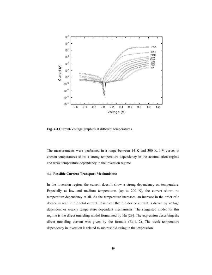
49
-0.6 -0.4 -0.2 0.0 0.2 0.4 0.6 0.8 1.0 1.210-13
10-12
10-11
10-10
10-9
10-8
10-7
10-6
10-5
10-4
10-3
Cur
rent
(A)
Voltage (V)
300K
270K210K180K150K120K90K60K30K
Fig. 4.4 Current-Voltage graphics at different temperatures
The measurements were performed in a range between 14 K and 300 K. I-V curves at
chosen temperatures show a strong temperature dependency in the accumulation regime
and weak temperature dependency in the inversion regime.
4.4. Possible Current Transport Mechanisms:
In the inversion region, the current doesn’t show a strong dependency on temperature.
Especially at low and medium temperatures (up to 200 K), the current shows no
temperature dependency at all. As the temperature increases, an increase in the order of a
decade is seen in the total current. It is clear that the device current is driven by voltage
dependent or weakly temperature dependent mechanisms. The suggested model for this
regime is the direct tunneling model formulated by Hu [29]. The expression describing the
direct tunneling current was given by the formula (Eq.1.12). The weak temperature
dependency in inversion is related to subtreshold swing in that expression.

50
In the accumulation part, it can easily be seen that two different mechanisms are competing
to dominate the total current in the device. One of these mechanisms depends strongly on
temperature. This mechanism plays an important role especially at high temperatures. It
also becomes dominant at low temperatures as the field in the oxide increases. The second
mechanism seems to be independent of temperature and dominant at low temperatures and
low fields. This field activated current doesn’t change with the temperature but it loses its
dominance as the temperature increases due to increase in temperature dependent current.
One should plot the Arrhenius plot to find out more about the temperature dependency of
the current. Semi-logarithmic plot of I vs. 1000/T plot for accumulation is seen in the
Fig.4.5:
0.000 0.005 0.010 0.015 0.020 0.025 0.030 0.03510-10
10-9
10-8
10-7
10-6
10-5
Cur
rent
(A)
1000/T (K-1)
0.2 volt 0.4 volt 0.6 volt 1 volt
Fig.4.5. Arrhenius plot at different gate voltages
As seen in the figure, the current depends exponentially on temperature. This is the case
especially for high temperatures. At lower temperatures, the Arrhenius curve exhibits little
dependence on temperature since field activated mechanism starts to contribute to total
current in more significantly. This effect is seen more clearly at 0.2 volt. Temperature
dependence is seen only at high temperatures. At medium and low temperatures, Arrhenius

51
curve is almost horizontal which means that current at those temperatures is due to field
activated carriers. Same conclusion can be obtained from Fig.4.5. At 0.2 V, field enhanced
current dominates until 120 Kelvin and from that point on, the current turns out to be a
temperature enhanced mechanism.
In addition to those two current regimes we explained above another current mechanism
can be identified in the results displayed in Fig.4.4. For higher voltages than 0.6 volt,
current-voltage curve shows a different behavior and becomes flatter. This can be seen for
higher temperatures more explicitly such as 300 K or 270 K. This behavior is due to series
resistance effect. We will get back to this point at the end of this chapter.
The suggested models for field activated current are Fowler-Nordheim and Schuegraf-Hu
direct tunneling model. Fowler-Nordheim model should be eliminated since it is widely
accepted that Fowler-Nordheim emission dominates at higher fields (more than 9-10
MeV/cm) and no higher field than 3-4 MeV/cm was applied in our measurements. The
direct tunneling model is more suitable than the Fowler-Nordheim model in our case. We
plotted ln (I/E2) vs. 1/E plots, so called Fowler-Nordheim plot, to make sure that the
tunneling type is direct rather than Fowler-Nordheim. There were two main regions in those
plots; a linear region with a negative slope at high fields and an almost linear region with a
positive slope at low fields. Also as the temperature decreases, qualitatively satisfactory
parts (high-field) produce steeper curves but the quantitative analyses reveal that this field
activated current is more likely to be direct tunneling from the substrate to the gate rather
than Fowler-Nordheim type tunneling. We derived the barrier height for tunneling from the
slopes of linear regions of Fowler-Nordheim plots. The barrier height values vary between
0.15 eV and 0.34 eV (higher barrier for lower temperature) with m*=0.42m0. These
variations are expected since as the temperature increases, the ratio of thermally excited
electrons gets higher and the effective barrier height decreases. The quantitative results for
Si-SiO2 system however are far from the commonly accepted values that vary between 3.0
eV or 3.15 eV. The shape of the Fowler-Nordheim plots and the extracted barrier heights
from those plots reveal that although Fowler-Nordheim tunneling might be occuring in our
system, it is not a dominant mechanism and the field activated component of the device
current should be direct tunneling from Silicon substrate to poly-Silicon gate for
accumulation.
The expression of direct tunneling formula for accumulation is [29];

52
( )[ ]
−−−−−
= 2/32
2
)/1(1exp/11
boxoxbox
DTt qVEB
qV
EAJ φ
φ (1.26)
where
b
oxo
hmmq
Aφπ8
)/(3
= ; qhm
B box
328 3φπ
= (1.24)
As was mentioned above, the gate current depends exponentially on 1/T. There are
basically four conduction processes in insulators which have exponential dependence on
temperature [1]:
Schottky emission:
−−= ∗
πεφ
4exp2 qE
kTqTAJ b (1.49)
Poole-Frenkel emission;
−−⋅⋅=
itPF
qEkTqEqnJ
πεφµ exp0 (1.37)
Band-to-band tunneling:
[ ]1)/exp()/exp()exp(2* −⋅−⋅−⋅= kTqVkTqTAJ GsbBTB φβφ (1.30)
Ohmic emission:
)/exp( kTEECJ a∆−⋅⋅= (1.39)
We studied Poole-Frenkel plots, ln (J/E) vs. E1/2, to determine which process is responsible
for the increase of current with temperature. The plots didn’t produce any significant
evidence of existence of Poole-Frenkel conduction. Curves were the type of second order
polynomials (i.e. parabolas) and deconvolution of oxide permittivity values from those rare

53
and narrow linear regions resulted in 10.1 ε0 to 24 ε0. It is obvious that these values are not
realistic when one takes the fact that Silicon dioxide permittivity is 3.8-3.9 ε0. Therefore
our conclusion was that Poole-Frenkel model is not an appropriate explanation for our
sample.
The last model we examined in search for thermal component of the device current was
band-to-band tunneling. This model is based on the Schottky diode theory. It describes the
tunneling thermal electrons in a MOS diode. Eq. 4.5 is identical to the standard thermionic
emission equation for Schottky barriers except a tunneling probability term. We were be
able to obtain very good results in our fit attempts by this model but the Schottky barrier
height (work-functions difference between the gate and the substrate) ,which is one of the
fit parameters, reduced mass in the oxide and the ideality factor, took unrealistic values for
our diode. The Schottky barrier height values were about 0.15 and 0.20 eV for successful
fits but in our structure this value has to be around 0.9 eV. When we used barrier height
values close to 0.90 eV, we couldn’t generate proper match between the experimental data
and the model. Therefore band-to-band tunneling model for the thermal current was
eliminated.
After all we concluded that thermal current is dominated by Schottky-like (thermionic)
emission. To be sure of our conclusion, we, for the last, studied two more plots and
compare them: one was J vs. E1/2 and the other was J/E vs. E1/2 at various temperatures. We
did this step to ensure that the thermal current mechanism is Schottky emission and not the
Poole-Frenkel. The existence of linearity in the first plot and variations in linearity in the
second plot are another proof that thermally activated current results from Schottky
emission.
4.5 Description of I-V curves:
Up to now, we used mostly qualitative methods to determine the current transport method
in our MOS capacitors. We also used more quantitative techniques to examine our results
further. We performed many fit attempts by using direct tunneling and thermionic emission
models both separately and together. During these attempts, we defined and used many fit
parameters and checked their physical meanings. All the details will be given in the
following sections.
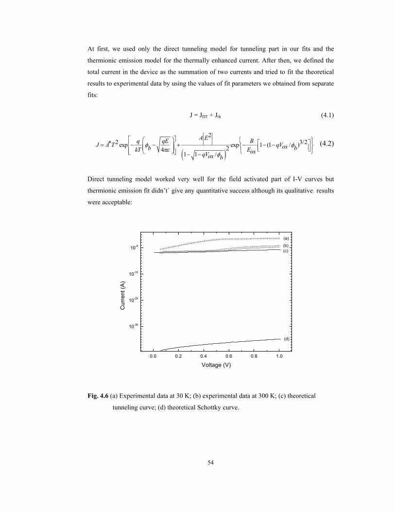
54
At first, we used only the direct tunneling model for tunneling part in our fits and the
thermionic emission model for the thermally enhanced current. After then, we defined the
total current in the device as the summation of two currents and tried to fit the theoretical
results to experimental data by using the values of fit parameters we obtained from separate
fits:
J = JDT + Jth (4.1)
( )
22 3/2exp exp 1 (1 / )24
1 1 /
A Eq qE BJ A T qVoxb bkT EoxqVox b
φ φπε
φ
∗ = − − + − − − − −
(4.2)
Direct tunneling model worked very well for the field activated part of I-V curves but
thermionic emission fit didn’t` give any quantitative success although its qualitative results
were acceptable:
0.0 0.2 0.4 0.6 0.8 1.0
10-38
10-28
10-18
10-8
Cur
rent
(A)
Voltage (V)
(a)
(b)(c)
(d)
Fig. 4.6 (a) Experimental data at 30 K; (b) experimental data at 300 K; (c) theoretical
tunneling curve; (d) theoretical Schottky curve.
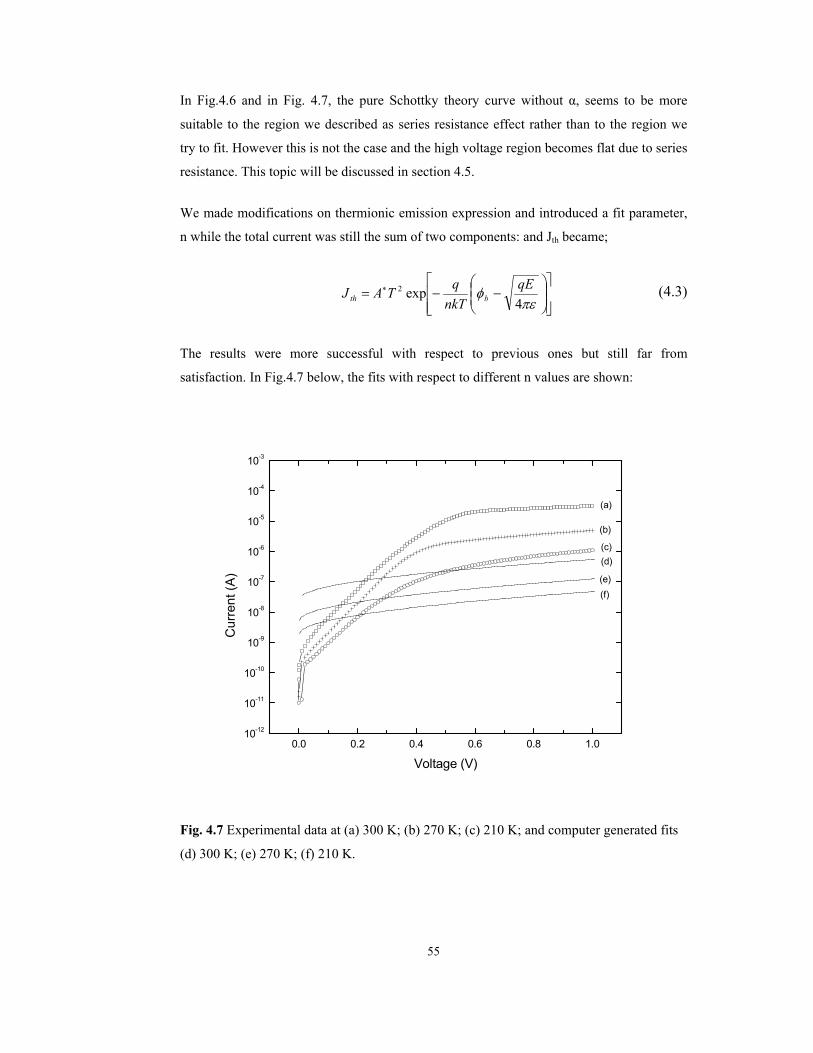
55
In Fig.4.6 and in Fig. 4.7, the pure Schottky theory curve without α, seems to be more
suitable to the region we described as series resistance effect rather than to the region we
try to fit. However this is not the case and the high voltage region becomes flat due to series
resistance. This topic will be discussed in section 4.5.
We made modifications on thermionic emission expression and introduced a fit parameter,
n while the total current was still the sum of two components: and Jth became;
−−= ∗
πεφ
4exp2 qE
nkTqTAJ bth (4.3)
The results were more successful with respect to previous ones but still far from
satisfaction. In Fig.4.7 below, the fits with respect to different n values are shown:
0.0 0.2 0.4 0.6 0.8 1.010-12
10-11
10-10
10-9
10-8
10-7
10-6
10-5
10-4
10-3
Cur
rent
(A)
Voltage (V)
(a)
(b)
(c)(d)
(e)(f)
Fig. 4.7 Experimental data at (a) 300 K; (b) 270 K; (c) 210 K; and computer generated fits
(d) 300 K; (e) 270 K; (f) 210 K.

56
After these results we decided to introduce another fit parameter to match the experimental
data and computer generated fits. The electric field factor due to image force lowering is
proportional to square root of electric field. We changed that power of ½ to a variable and
labeled it as alpha, α. We made new fit attempts using the new expression of current and
the results, this time, were much more better and satisfactory. The total current, therefore,
we used in our fits became;
( )* 2
2 3/22exp exp 1 (1 / )
4 1 1 /b ox b
oxox b
A R Eq q BJ A R T E qVnkT EqV
αφ φπε φ
∗ ⋅ ⋅
= ⋅ ⋅ − − + − − − − − (4.4)
Where A is the device area and R* is Richardson constant;
b
oxo
hmmq
Rφπ8
)/(3
= ; qhm
B box
328 3φπ
= (4.5)
In this expression there are two active fit parameters; n and α; and four passive fit
parameters: carrier mass in the oxide, barrier height, oxide permittivity and device area. We
chose the passive fit parameters at the beginning of each fit attempt and kept them constant
during that fit session. We changed only the temperature and active parameters during the
fit process.
Among many attempts, we found three different sets presentable. In these fits, we used
different values for both active and passive parameters and tried to obtain the best match
between the theory and the experimental data. The details of these fits and the values of the
parameters are as follows;
Set 1:
Table 4.1 Passive fit parameters for set-1
Permittivity ε 3.9 ε0 (ε0 = 8.85x10¹² C2/N•m2)
Oxide thickness d 30 Angstrom
Reduced mass m 0.47 m0 (m0 = 9.1x10⁻³¹ kg)
Barrier height Φb 3.05 eV
Area A 550x550 µm2

57
0.0 0 .2 0 .4 0 .6 0 .8 1 .010 -11
10 -10
10 -9
10 -8
10 -7
10 -6
10 -5
10 -4
Cur
rent
(A)
V o ltage (V )
(a)
(b )
(c )(d)(e)
Fig. 4.8 Fits at (a) 300 K; (b) 270 K; (c) 210 K; (d) 180 K; (e) 150 K with parameters of
set1.
0 .0 0 .2 0 .4 0 .6 0 .8 1 .0
10 -10
10 -9
10 -8
10 -7
10 -6
Cur
rent
(A)
V o lta g e (V )
(a )
(b )
(c )(d )(e )
Fig. 4.9 Fits at (a) 150 K; (b) 120 K; (c) 90 K; (d) 60 K; (e) 30 K with parameters of set1.
The active parameters in this set are: Temperature (in Kelvin), n and α:

58
Table 4.2 The active fit parameters for Set-1
T 300 270 210 180 150 120 90 60 30
n 3.52 3.78 4.75 5.35 6.10 7.30 9.50 14.0 27.0
α 0.58 0.58 0.58 0.58 0.58 0.58 0.58 0.58 0.58
The observed characteristics of our MOS capacitor are separated into two parts as we
mentioned above; thermionic characteristics with temperature and tunneling characteristics.
These two transport processes are seemed to be competing mechanisms. The tunneling
component can be accepted as a base current for the device. It follows only the changes in
the field in the oxide and it is not affected by the variations in the temperature since its
dependence on temperature is very weak. As the temperature increases thermionic current
becomes dominant process and I-V curve looks like more and more pure Schottky emission
curve. However Schottky mechanism is not just a temperature dependent mechanism but it
also depends on voltage. As the voltage exceeds a threshold value the thermionic current
becomes greater than the tunneling current and it overtakes the tunneling current. The
threshold value should decrease as the temperature increases.
The tunneling current dominates the device characteristics at low temperatures up to 90
Kelvin. However, at medium temperatures from 120 Kelvin to 210 Kelvin, we see a
transition from tunneling to thermionic current and the total current in the device is
determined by the two components almost at the same amount. Under the light of these
observations, we employed our defined total current with modifications to Schuegraf-Hu
direct tunneling and Schottky emission models. At high temperatures such as 300 K or 210
K, there was an exact match between the experimental data and the generated data up to 0.6
volts. After this voltage series resistance effect becomes important. Since the device current
is deeply affected by this phenomenon, we see big differences between the experimental
data and model calculations. At very low temperatures, fits gave very good results for the
tunneling and acceptable results for thermionic current. It was also observed that the
voltage at which thermionic process starts to dominate decreases as the temperature
increases. For example this threshold value is about 0.5 volts for 30 K and it decreases up to
0.2 volts at 120 K. The series resistance effect again dominates the high voltage regimes
and it doesn’t allow thermionic current to last long and it causes the thermionic current to
rule the total current for a very short voltage interval. This interval is about, for example,

59
0.2 volts (0.5 to 0.7) for 30 K, 0.2 volts (0.3 to 0.5) for 60 K and 0.25 volts (0.15 to 0.4) for
150 K. This change from thermionic characteristics to series resistance effect in the
observed current makes it difficult to make perfect fits to thermionic current component
part of the total current for especially low temperatures.
The medium temperatures are the most important ones for our approach since we can see
the transition between tunneling and thermionic currents for a, relatively, long voltage
interval. We see from Fig.4.10 and Fig.4.12 that the fit results are very satisfactory at 120
K, 150 K and 180 K. The calculated total current shows a smooth transition from base
tunneling region to up thermionic region very successfully.
The values of passive fit parameters are given in table 4.1 and table 4.2 above. The
permittivity is chosen as 3.9 ε0 which is universally accepted for SiO2, and the device area
(or the gate area) was measured as 550x550 (µm2). These two parameters were kept
constant for all the fits we did. The other three parameters were decided at the beginning of
each fit. There is no consensus on some constant carrier mass value. The oxide mass values
show great differences in different works in scientific literature. The values vary from 0.32
m0 to 0.55 m0 for electron mass and from 0.25 to 0.32 m0 for hole mass. In this work we
used three different mass values as fit parameters. In this set the carrier mass was 0.47 m0
(electron). And the barrier height at the interface of Si/SiO2 was chosen to be 3.05 eV. This
is a suitable value as the commonly used values range from 2.95 eV to 3.15 eV for Si-SiO2
system. This value was chosen for both the tunneling barrier height which electrons feel
while they tunnel from Si substrate to poly-Si gate and the thermionic barrier height that the
electrons must overcome thermally to pass to the conduction band of SiO2.
The active parameters are n, a factor some groups call it as barrier lowering coefficient
[76], and α, the image force lowering factor. The meanings of these factors will be
discussed at the end of this section and therefore only the numerical values of them will be
mentioned here. Alpha, α, was kept constant at a value of 0.58 while n changes from 3.52 to
27.0. At high temperatures n values were lower and n becomes greater as the temperature
decreases. At high temperatures, n changes adiabatically but this change turns to be abrupt
as the temperature decreases. For example, from 300 K to 270 K, change in n is 0.26 and
0.6 for 210 K to 180 K, and 1.2 for 150 to 120 K. For very low temperatures n values reach
very high values (especially for 30 K). This is probably due to the fact that the thermionic
component is negligible at these temperatures and a fit attempt by using this model is not
meaningful.

60
SET 2
The details are as below for this fit attempt:
Table 4.3 The passive fit parameters.
Permittivity ε 3.9 ε0 (ε0 = 8.85x10¹² C2/N•m2)
Oxide thickness d 30 Angstrom
Reduced mass m 0.467 m0 (m0 = 9.1x10⁻³¹ kg)
Barrier height Φb 3.1 eV
Area A 550x550 µm2
Table 4.4 The active fit parameters.
T 300 270 210 180 150 120 90 60 30
n 3.60 3.87 5.05 5.42 6.25 6.85 8.75 12.7 24.2
α 0.58 0.58 0.57 0.58 0.58 0.59 0.59 0.59 0.59
0 .0 0 .2 0 .4 0 .6 0 .8 1 .0 1 .21 0 -1 1
1 0 -1 0
1 0 -9
1 0 -8
1 0 -7
1 0 -6
1 0 -5
1 0 -4
Cur
rent
(A)
V o lta g e (V )
(a )
( b )
( c )(d )(e )
Fig.4.10 Fit plots at (a) 300 K; (b) 270 K; (c) 210 K; (d) 180 K; (e) 150 K with parameters
of set2.

61
0.0 0.2 0.4 0.6 0.8 1.0
10-10
10 -9
10 -8
10 -7
10 -6
Cur
rent
Vo ltage
(a)(b)
(c)
(d)
(e)
Fig.4.11 Fits at (a) 150 K; (b) 120 K; (c) 90 K; (d) 60 K; (e) 30 K with parameters of set2.
In the second set of fit, we set the barrier height as 3.1 eV and m* as 0.467 m0. The most
notably difference in this try with respect to previous one is that α was not kept constant. It
was allowed to change. By doing so we aimed to have better fits to the experimental data.
The result was not much different from the previous fit set. Almost the same characteristics
were obtained. The details are below:
SET 3
In the last fit attempt we present, we used the oxide thickness as 28 Angstrom rather than
30 ± 2 Angstroms. We modified almost all the parameters except the permittivity. Image
force lowering parameter α was chosen to be variable as it was in the second fit set. The
active and passive fit parameters are:
Table 4.5 The active fit parameters for set-3.
T 300 270 210 180 150 120 90 60 30
n 3.4 3.62 4.75 5.38 5.80 7.0 8.0 11.5 25.5
α 0.58 0.58 0.57 0.57 0.58 0.58 0.59 0.59 0.58

62
Table 4.6 The passive fit parameters for set-3
Permittivity ε 3.9 ε0 (ε0 = 8.85x10¹² C2/N•m2)
Oxide thickness d 28 Angstrom
Reduced mass m 0.55 m0 (m0 = 9.1x10⁻³¹ kg)
Barrier height Φb 3.0 eV
Area A 550x550 µm2
And the fit results are for these parameters are:
0.0 0.2 0.4 0.6 0.8 1.010-11
10-10
10-9
10-8
10-7
10-6
10-5
10-4
Cur
rent
(A)
Voltage (V)
(a)
(b)
(c)(d)(e)
Fig.4.12 Fit plots at (a) 300 K; (b) 270 K; (c) 210 K; (d) 180 K; (e) 150 K with parameters
of set3.

63
0.0 0.2 0.4 0.6 0.8 1.0
10-10
10-9
10-8
10-7
10-6
Cur
rent
Voltage
(a)(b)
(c)
(d)
(e)
Fig.4.13 Fits at (a) 150 K; (b) 120 K; (c) 90 K; (d) 60 K; (e) 30 K with parameters of set3.
This set was little bit more successful than the other two ones but there was no significant
change from the previous two ones. The main difference in this set was in the match at low-
medium temperatures, 120 K and 90 K. The fits produced better results but in this region.
At the end of these three results, it can be said that all of them produce similar results with
some minor differences. All the three sets were very successful at high and medium
temperatures and they also gave good and acceptable results at low temperatures. Therefore
none of them is preferable in this manner.
Also all the fits turned out to be successful with almost the same fit parameter values. For
the passive fit parameters, all the values are in acceptable ranges, for example barrier height
change between 3.0 eV and 3.15 eV or oxide mass between 0.47 to 0.55 m0. And for the
active parameters, image force lowering power α is centered on 0.58 for all the three fits.
Although in other fit attempts we set this parameter up to different values from 0.54 to 0.61,
the best fits were obtained by using 0.57, 0.58 and 0.59. The situation is also similar for the
barrier height lowering parameter, n. This value starts from 3.52 in set1, 3.60 in set2, 3.4 in
set3 and go up to 27.0 in set1, 24.2 in set2, and 25.0 in set3. Also, the increase in n between

64
two temperature increases at lower temperatures in all three sets. Set3 is little bit better in
terms of n since it keeps n at 11.7 at 60 K.
4.6. Conclusion
The current-voltage characteristics of ultra-thin oxide capacitor was found to be
temperature dependent in accumulation and tunneling in inversion. This case has also been
observed by many other groups [76-88] and there is a growing interest in temperature
dependent measurements in both cryogenics and high temperatures due to new advances in
superconducting circuits and high temperature applications. The main questions about our
modification on Schottky emission theory and our fit procedure at this point are the
physical meaning of those fit parameters and their numerical values. What do these
parameters imply and are they meaningful with these values?
This is a common method in I-V analysis that one changes the main parameters in a
suitable conduction mechanism and set some parameters adjustable if one thinks that that
mechanism occurs in the device but does not exactly match with the experimental data.
Although some authors do this step without giving valid physical explanations and they
approach to the problem from a purely mathematical point of view, we believe that all these
parameters have to carry some physical meanings. In this work we introduced two basic
parameters; n and α.
The barrier height parameter n decreases the weight of thermionic current as the
temperature decreases just like as the ideality factor does in Schottky junctions. At low
temperatures n goes higher and it reduces the thermionic current and allows the base
tunneling current to show up more. Therefore n, in this manner, is very much like an
ideality factor but the main difference between n and an ideality factor is that ideality factor
is related with the voltage in the device. The ideality factor approaches unity if the applied
voltage in a device is completely taken by the oxide. If some of the applied voltage falls on
out of oxide then the ideality factor increases. However in our case, n is applied to barrier
height and it somehow defines a new effective barrier value for the thermionic emission.
The interesting point here is the effective barrier height decreases as the temperature
decreases. It is expected that the barrier height decreases and hence the thermionic current
increases as the temperature increases. However, if one considers the carrier distribution in
the conduction band of the substrate and takes n as an implication of the carriers that can
overcome the barrier, then as the temperature decreases the number of the carriers which

65
can get over the barrier and pass through the SiO2 conduction band decreases which
corresponds to the increase in n with decreasing temperature
Another explanation for the barrier lowering factor can be done from the view point of
tunneling current. The factor n can behave the way it reduces the tunneling barrier and
causes more carriers to be able to tunnel through the oxide.
Another conclusion can be made about inhomogeneous barriers. The temperature
dependency of n can be attributed to lateral inhomogeneous barrier distribution over the
device area. It means that not all the points in the device have the physical structure. Some
of the regions contain small patches so that the barrier height in these regions is slightly
different than the accepted barrier heights. This difference however should be small and the
distribution can be described by a Gaussian curve centered on the accepted values, which
are in our fits 3.0 eV, 3.05 eV and 3.15 eV.
The values which n took in our fits are reasonable and compatible with other works [76].
Yassine and Hijab found n as 3.7 in their paper. This is very close to our n which takes ~3.5
at 300 K in our fits.
The second fit parameter is α. In many reference books it can be found about image force
lowering of barrier due to carriers injected to oxide conduction band. In these theories, the
interaction between the injected carriers and the oxide matrix is assumed to be Coulombic.
However in reality, the oxide is not perfect as it was assumed and the interactions are much
more complex due to inhomogeneity of the oxide. There are oxide charges as well as
surface states which destroy the presupposed homogeneity and make the interactions
complex. We believe that the change in α from 0.50 to 0.58 and so on corresponds to this
complexity.
Another idea about α could be that the oxide might not be uniform for all the interface
region of Si/SiO2. Some points might be much more thinner than 30 Angstroms and it could
lead a device behavior like a pn junction rather than MOS structure.
The final words about the I-V characteristics will be on the series resistance. At high
voltages at all temperatures series resistance effect plays important role in our I-V results as
seen in Fig.4.4. At high temperatures such as 300 K or 270 K, this effect is seen after 0.5-
0.6 volts and at lower temperatures (i.e. 30 K) it starts to be active from about 0.7 volts. I-V
curves start to become parallel after these points at the mentioned temperatures and device

66
is driven to an ohmic characteristics. At this point we should avoid confusion; one might
think of the Fig.4.5 and get confused since the original thermionic theory curve
qualitatively looks like to the curve we label as series resistance as we mentioned in section
4.3 To make this point clear one should plot another type of Arrhenius curve: J/T2 vs. 1/T
assuming Schottky emission described by Eq.4.3. This plot gives such results as in Fig.
4.14:
0.000 0.005 0.010 0.015 0.020 0.025 0.030 0.03510-14
10-13
10-12
10-11
10-10
log
I/T2 (A
/K2 )
1000/T (K -1)
(a)
(b)
(c)(d)(e)
Fig.4.14 The second type Arrhenius plots at (a) 1 v; (b) 0.6 v; (c) 0.5 v; (d) 0.4 v; (e) 0.2 v.
When we compare Fig.4.5 and Fig.4.14 we see there are basic differences in all the plots at
different voltages. In the Fig.4.5 it was observed that two different temperature dependency
regions exist for high voltages (0.6 and 1 volts). At high temperatures the Arrhenius curve
is steeper and for low temperatures this curve becomes smoother but still exists. After
reading this information from the Fig.4.5, one can easily say that the dominant mechanism
is certainly the thermionic emission for medium and high temperatures. And for low
voltages such as 0.2 or 0.4 volts, two different behaviors can be identified; one part of the
curve shows a strong temperature dependency and the other shows almost no temperature
dependency. This indicates that at high voltages, a temperature dependent mechanism is
dominant, for example thermionic emission at 300 K, but at low voltages the current is
contributed by a field activated mechanism, i.e. 30 K.

67
Another interesting note about this point is that we tried to make a suitable fit to high field
I-V curve at 300 K by using the thermionic emission. The successful result was obtained by
letting α be 0.48. We believe that although α can be greater than 0.5 and this can be
explained as we did above, it shouldn’t be less than 0.48. Therefore, under the light of these
discussions we believe that our first conclusion is correct and the high fields I-V
characteristics are contributed by series resistance affect at all the temperatures. Also as it is
expected, series resistance is seen at lower fields at higher temperatures with respect to
lower temperatures.

68
REFERENCES
[1] S. M. Sze, Physics of Semiconductor Devices, John Wiley & Sons, 2nd ed., 1981.
[2] Nicollian E.H. and Brews J.H., MOS (Metal Oxide Semiconductor) Physics and
Technology, 1982.
[3] B. Van Zeghbroeck, Principles of Semiconductor Devices, 2004.
[4] Fonstad C. G., Microelectronic Devices and Circuits, McGraw-Hill, 1994.
[5] R. Fowler and L. Nordheim, “Electron emission in intense electric fields”, Proc. Roy.
Soc. A, vol. 119, pp. 173-181, 1928.
[6] Lenzlinger F.M. and Snow E.H., “Fowler-Nordheim tunneling into thermally grown
SiO2”, J. Appl. Phys., 1969, 40, 278.
[7] Osburn C.M. and Weitzman E.J., “Electrical construction and dielectric breakdown
in silicon dioxide films on silicon”, J. Elec. Soc., 1972, 119, 603.
[8] Maserjian J., “Tunneling in thin MOS structures”, J. Vac. Sci., 1974, 11(6), 996.
[9] Shatzkes M. and Av-Ron M., “Impact ionization and positive charge in thin SiO2
films”, J. Appl. Phys., 1976, 43, 3191.
[10] Weinberg Z.A., “Tunneling of electron from Si into thermally grown SiO2”, Solid-
State Electronics, 1977, 20, 11.
[11] Av-Ron M., Shatzkes M., Distefano T.J., Gdula R.A., “Electron tunneling at Al-SiO2
interface”, J. Appl. Phys., 1984, 52(4), 2897.
[12] Krieger G., Swansson R.M., “Fowler-Nordheim electron tunneling in thin Si-SiO2-Al
structures”, J. Appl. Phys. 1981, 52, 5710.
[13] Weinberg Z.A., “On the tunneling in metal-oxide-silicon structure”, J. Appl. Phys.
1982, 53, 5052.
[14] Chang C. Brodersen R.W., Hu C., “Insulating films in semiconductors”, Amsterdam,
North Holland, 1983, p.717.

69
[15] Nissan-Cohen Y., Shappir J. Frohman-Bentchkowsky D., “Measurement of Fowler-
Nordheim tunneling currents in MOS structures under charge trapping conditions”,
Solid-State Electronics, 1985, 28, 717.
[16] Kong S.O., Kwok C.Y., “Fowler-Nordheim tunneling current in a Mg/Polycrystallin
Si oxide/n- polycrystalline Si metal-oxide-silicon structure”, Appl. Phys. Lett. 1993,
63(19), 2667.
[17] Olivo P. Sune J. Ricco B., “Determination of the Si-SiO2 barrier height from the
Fowler-Nordheim plot. IEEE Electron Dev. Lett. 1991, 12, 620.
[18] Chiou Y.L., Gambino J.P., Mohammad M., “Determination of the Fowler-Nordheim
tunneling parameters from the Fowler-Nordheim plot”, Solid-State Electronics, 2001,
45, 1787.
[19] Depas M., Vermeire B., Mertens P.W., Van Meirhaeghe R.L., Heyns M.M.,
“Determination of the tunneling parameters in ultra-thin oxide layer Poly-Si/SiO2/Si
structures”, Solid-State Electronics, 1995, 38, 1465.
[20] Lo S.L., Buchanan D., Taur Y., Wang W., “Quantum mechanical modeling of
electron tunneling current from the inversion layer of ultra-thin oxide nMOSFETs”,
IEEE Electron Dev. Lett. 1997, 18, 209.
[21] Bowen C., Fernardo C., Klimeck G., Chatterjee A., Blanks D., Lake R., Hu J., Davis
J., Kulkarni M., Hattangady S., Chen I., “Physical oxide thickness extraction and
verification using quantum mechanical simulation”, IEDM Technical Digest, 1997,
p.869.
[22] Sune J., Olivo P. Ricco B., “Self-consistent solution of Poisson and Schrödinger
equations in accumulated semiconductor-insulator interfaces”, J. Appl. Phys. 1991,
70, 337.
[23] Rana F., Tirwari S., Buchanan D., “Self-consistent modeling of accumulation layers
and tunneling currents through very thin oxides”, Appl. Phys. Lett. 1996, 69(8),
1104.
[24] Yang. N., Henson W., Hauser J., Wortman J., “Modeling study of ultra-thin gate
oxides using direct tunneling current and capacitance-voltage measurements in MOS
devices”, IEEE Trans. Electron Dev., 1999, 46(7), 1464.
70
[25] Register L., Rosenbaum E., Yang K., “Analytic model for direct tunneling in
polycrystalline silicon gate metal-oxide-semiconductor devices”, Appl. Phys. Lett.,
1999, 74(3), 457.
[26] Yang K.N., Huang H.T., Chang M.C., Chu C.M., Chen Y.S. Chen M.J., Lin Y.M.,
Yu M.C., Jang S., Yu D., Liang M., “A physical model for hole direct tunneling
current in P+ poly-gate PMOSFETS with ultra-thin gate oxides”, IEEE Trans.
Electron Dev., 2000, 47(11), 2161.
[27] Ghetti A., “Characterization and modeling of the tunneling current in Si-SiO2-Si
structures with ultra-thin oxide layer”, Microelectronic Engineering, 2001, 59, 127.
[28] Schuegraf K.F., King C.C., Hu C., Digest Symposium on VLSI, IEEE, New York,
1992, pp.18.
[29] Lee W.C. and Hu C., “Modeling gate and substrate currents due to conduction and
valence band electron and hole tunneling”, Digest Symposium on VLSI Technology
Digest of Technical Papers, IEEE, New York, 2000, pp.198.
[30] Timp G. et al., “Process toward 10-nm CMOS devices,” in IEDM Tech. Dig., 1998,
pp. 615–618.
[31] Hou Y. T., Lia M. F., Jin Y., and Lai W. H., “Direct tunneling hole currents through
ultra-thin gate oxides in metal-oxide-semiconductor devices”, J. Appl. Phys. vol.91,
No.1, 2002.
[32] Lo S. H., Buchanan D. A. and Taur Y., “Modeling and characterization of
quantization, polysilicon depletion, and direct tunneling effects in MOSFETs with
ultrathin oxides”, IBM J. Res. Develop. vol.43 No.3, 1999.
[33] Clerc P., Sullivan P. O., McCarthy K. G., Ghibaudo G., Pananakis G., Mathewson
A., “A physical compact model for direct tunneling from NMOS inversion layers”,
State Electronics, 2001, vol. 45, p.1705.
[34] Lee J., Bosman G., Green K. R., and Ladwig D., “Model and analysis of gate leakage
current in ultra-thin nitrided oxide MOSFETs”, IEEE Trans. Electron Dev., 2002,
49(7).
[35] Mao L., Tan C., and Xu M., “The effect of image potaential on electron transmission
and electric current in the direct tunneling regime of ultra-thin MOS structures”,
Microelectronics Reliability, 2001, 41, p.927.

71
[36] Sheu C-Y., and Jang S-L., “A physics-based electron gate current model for fully
depleted SOI MOSFETs”, Solid-State Electronics, 2000, 44, p.1799.
[37] Bhattacharya S. S., Banarjee S. K., Nguyen B. Y, and Tobin P. J., “Temperature
dependence of the anomalous leakage current in poly-silicon-on-insulator
MOSFETs”, IEEE Trans. Electron Dev., 2002, 41 (2).
[38] Sullivan P. O., Clerc P., McCarthy K.G., and Ghibaudo G., “Direct tunneling models
for circuit simulation”, Microelectronics Reliability, 2001, 41, p.951.
[39] Hsu B. C., Chen K. F., Lai C. C., Lee S. W., and Liu C. W., “Oxide roughness effect
on tunneling current of MOS diodes”, IEEE Trans. Electron Dev., 2002, 49 (12).
[40] Chen L., Ma Y., and Tian L., “Modeling on direct tunneling current in ultra-thin
oxide NMOSFET considering quantum mechanics”, Proc. 23rd International
Conference on Microelectronics, vol.2, NIS, Yugoslavia, 2002.
[41] Ghetti A., Bude J., Silverman P., Hamad A., and Vaidya H., “Modeling and
simulation of tunneling current in MOs devices including quantum mechanical
effects”, IEICE Trans. Electron., 2000, vol.E83-C, No.8, p.1175.
[42] Wettstein A., Schenk A., Scholze A., and Fichtner W., “The influence of localized
states on gate tunnel currents: Modeling and simulation”, SISPAD Tehc. Dig., 1997,
p.101.
[43] Gupta A., Fang P., Song M., Lin M-R., Wollesen D., Chen K., and Hu C., “Accurate
determination of ultra-thin gate oxide thickness and effective poly-silicon doping of
CMOS devices”, IEEE Trans. Electron Dev., 1997, 18(12).
[44] Miranda E., Redin G., and Faigon A., “Modeling of the I-V characteristics of high-
field stressed MOS structures using a Fowler-Nordhei type tunneling expression”,
Microelectronics Reliability, 2002, 42, p.935.
[45] Choi C-H., Nam K-Y., Yu Z., and Dutton R. W., “Impact of gate direct tunneling
current on circuit performance: A simulation study”, IEEE Trans. Electron Dev.,
1999, 48(12), 2823.
[46] Cova P., Singh A., and Masut R. A., “Simultaneous analysis of current-voltage and
capacitance-voltage characteristics of metal-insulator-semiconductor diodes with a
high mid-gap trap density”, J. of Appl. Phys. vol.85, No.9, 1999.

72
[47] Magnus W., and Schoenmaker W., “Full quantum mechanical model for the charge
distribution and the leakage currents in ultra-thin MOS capacitors”, J. App. Phys., 88
(10), p.5833.
[48] Iwata H., Matsuda T., and Ohzone T., “Two-dimensional self-consistent calculation
of gate direct tunneling current in metal-oxide-semiconductor transistors”, Jap. J. of
Appl. Phys. Part-1 Regular Papers Short Notes & Review Papers, 42(6A), p.3364.
[49] Card H.C. and Rhoderick E.H., “Studies of tunnel MOS diodes I. Interface effects on
silicon Schottky diodes”, J. Phys. D: Appl. Phys., 1971, vol.4, 1589.
[50] Card H.C. and Rhoderick E.H., “Studies of tunnel MOS diodes II.Thermal
equilibrium considerations”, J. Phys. D: Appl. Phys., 1971, vol.4, 1602.
[51] Kumar V. and Dahlke W.E., “Characteristics of Cr-SiO2-nSi tunnel diodes”, Solid-
State Electronics, 1977, vol. 20, p.143.
[52] Wu J., Register L., Rosenbaum E., “Trap assisted tunneling current through ultra-thin
oxide”, Proc. IRPS Symposium, 1999, pp.389-395.
[53] Ghetti A., Alam M., Bude J., Sangiogi E., Timp G., Weber G., “Native and stress
induced traps in SiO2 films”, Proc. Of the 4th Symposium on the Physics and
Chemistry of SiO2 and the Si-SiO2 interface, Toronto, Canada; 2000, pp.419-428.
[54] Takagi S., Yasuda A., Torimu A.,”A new model for stress induced leakage current
including inelastic tunneling”, IEEE Trans. Electron Dev., 1999, 46(2), 348.
[55] Fleischer S., Lai P.T., Cheng Y.C., “A new method for extracting the trap energy in
insulators”, J. Appl. Phys., 1993, 73(1), 3348.
[56] Fleischer S., Lai P.T., Cheng Y.C., “Effects of nitridation temperature on the electron
trap characteristics of nitrided-oxide metal-oxide-semicondcutor capacitors”, J. Appl.
Phys., 1993, 74(1), 740.
[57] Ricco B. and Azbel M. Y., “Physics of resonant tunneling: The one-dimensional
double-barrier case”, Phys. Rev. B, 1984, vol. 29, no. 4, p.1970
[58] J.P. Sorbier J.P., Croci S., Imbert B., and Plossu C., “Model of leakage current
induced by dynamic stress in thin EEPROM tunnel oxides”, J. of Non-Crystalline
Solids, 2003, 322(1-3), p.122.
[59] Takagi S., Yasuda N., and Toriumi A., “A new I-V model for stress-induced leakage
current including inelastic tunneling”, IEEE Trans. Electron Dev., 1999, 46(2),
p.348.

73
[60] Buttiker M., “Coherent and sequential tunneling in series barriers”, IBM J. Res.
Develop., 1988, vol. 32, p.63.
[61] Ricco B., Gozzi G., Lanzoni M., “Modeling and simulation of stress induced leakage
current in SiO2 films”, IEEE Trans. Electron Dev., 1998, 45(7), 1554.
[62] Okada K. and Taniguchi K., “Electrical stress-induced variable range hopping
conduction in ultrathin silicon dioxides”, Appl. Phys. Lett. 1997, 70, 351.
[63] Suzuki E. and Schroeder D.K., J. Appl. Phys., 1986, 60, 3616.
[64] Cheng X.R., Cheng Y.C., Liu B.Y., J. Appl. Phys., 1992, 72, p.5711.
[65] Houng M.P., Yeong H.W., Chang W.J., “Current transport mechanism in trapped
oxides: A generalized trap assisted tunneling model”, J. Appl. Phys., 1999, vol.86
(3), 1488.
[66] Chou A.I., Lai K., Kumar K., Chowdhury P., and Lee J.C., “Modeling of stress-
induced leakage current in ultrathin oxides with the trap-assisted tunneling
mechanism”, Appl. Phys. Lett., 1997, 70(25), p.3407.
[67] Ng K.K., Comlete Guide to Semiconductor Devices, 1995, McGraw-Hill Inc.
[68] Bethe H. A., “Theory of the Boundary Layer of Crystal Rectifiers” MIT, Radiat. Lab.
Rep. 43-12, 1942.
[69] Freeman L.B. and Dahlke W.E., “Theory of tunneling into interface states”, Solid-
State Electronics, 1970, vol.13, 1483.
[70] Dogish M.Y. and Ho F.D., “A comprehensive analytical model for metal-insulator-
semiconductor (MIS) devices”, 1992, IEEE Trans. Electron Dev., vol.39, 2771.
[71] Hovel H.J., Semiconductors and Semimetals, vol.11: Solar Cells. NY Academic
Press, 1975.
[72] Jacop A.P. et. al. Semiconductor Science and Technology, 2002, 17(9), 942.
[73] Schroder D.K., Semiconductor Material and Device Characterization 2nd ed., 1998,
John Wiley & Sons Inc.
[74] Krisch K.S., Bude J.D. and Manchanda L., “Gate Capacitance Attenuation in MOS
devices With Thin Dielectrics”, IEEE Electron Dev. Lett., 1996, 17, 521.
[75] Vasileska D., Schroder D.K. and Ferry D.K., “Scaled Silicon MOSFET’s:
Degradation of the Total Gate Capacitance”, IEEE Trans. Electron Dev., 1997, 44,
584.

74
[76] Yassine A., and Hijab R., “Temperature dependence of gate current in ultra-thin SiO2
in direct tunnelling regime”, Integrated Reliability Workshop Final Rep., 1997, p.56.
[77] Lin C.H., Hsu B.C., Lee M.H., and Liu C.W., “A comprehensive study of inversion
current in MOS tunnelling diodes”, ”, IEEE Trans. Electron Dev., 2001, 48(9).
[78] Jacob A. P., Mryberg T., Nur O., Willander M., Lundgren P., Sveinbjörnsson E. Ö.,
Ye L. L., Thölen A. and Caymax M., “Cryogenic performance of ultra-thin oxide
MOS capacitors with in situ doped p+ poly-Si1-xGex and poly-Si gate materials”,
Semiconductor Science and Technology, 2002, 17, p.942.
[79] Houssa M., Aoulaiche M., Autran J. L., Parthasarathy C., Revil N., and Vincent E.,
“Modeling negative bias temperature instabilities in hole channel metal-oxide-
semiconductor field effect transistors with ultrathin gate oxide layers”, J. of Appl.
Phys., 2004, 95(5), p.2786.
[80] Pananakakis G., Ghibaudo G., Kies R., Papadas C., “Temperature dependence of the
Fowler-Nordheim current in metal-oxide-degenerate semiconductor structures”, J
Appl. Phys., 1995, 78(4), p.2635.
[81] Schroeder D., and Avellan A., “Physical explanation of the barrier height
temperature dependence in metal-oxide-semiconductor leakage current models”,
Appl. Phys. Lett., 2003, 82 (25), p.4510.
[82] Hadjadj A., Simonetti O., Maurel T., Salace G., and Petit C., “Si-SiO2 barrier height
and its temperature dependence in metal-oxide-semiconductor structures with
ultrathin gate oxide”, Appl. Phys. Lett., 2002, 80(18), p.3334.
[83] Hadjadj A., Salace G., and Petit C., “Fowler-Nordheim conduction in polysilicon
(n(+))-oxide-silicon (p) structures: Limit of the classical treatment in the barrier
height determination”, J. of Appl. Phys. , 2001, 89 (12), p.7994.
[84] Larcher L., Paccagnella A., and Ghidini G., “Gate current in ultrathin MOS
capacitors: A new model of tunnel current”, IEEE Trans. Electron Dev., 2001, 48(2),
p.271.
[85] Salace G., Hadjadj A., Petit C., and Ziane D., “The image force effect on the barrier
height in MOS structures: correlation of the corrected barrier height with temperature
and the oxide thickness”, Microelectronics Reliability, 2000, 40(4-5), p.763..

75
[86] Waters R., and Van Zeghbroeck B., “Temperature-dependent tunneling through
thermally grown SiO2 on n-type 4H-and 6H-SiC”, Appl. Phys. Lett., 2000, 76 (8),
p.1039.
[87] Salace G., Hadjadj A., Petit C., and Jourdain M., “Temperature dependence of the
electron affinity difference between Si and SiO2 in polysilicon (n(+))-oxide-silicon
(p) structures: Effect of the oxide thickness”, J. of Appl. Phys., 2001, 85 (11), p.7768.
[88] Liu Y., Chen T.P., Ang C.H., and Fung S., “Power-law dependence of charge
trapping on injected charge in very thin SiO2 films”, Jap. J. of Appl. Phys. Part-2
Letters, 2002, 41 (4A), L384.