electrochromics for smart windows: thin films of tungsten ...42086/fulltext01.pdf ·...
TRANSCRIPT

Electrochromics for smart windows: thin films of tungsten oxide and nickeloxide, and devices based on these
Gunnar A. Niklasson and Claes G. Granqvist
Received 23rd August 2006, Accepted 13th October 2006
First published as an Advance Article on the web 8th November 2006
DOI: 10.1039/b612174h
Electrochromic (EC) materials are able to change their optical properties, reversibly and
persistently, by the application of an electrical voltage. These materials can be integrated in
multilayer devices capable of modulating the optical transmittance between widely separated
extrema. We first review the recent literature on inorganic EC materials and point out that today’s
research is focused on tungsten oxide (colouring under charge insertion) and nickel oxide
(colouring under charge extraction). The properties of thin films of these materials are then
discussed in detail with foci on recent results from two comprehensive investigations in the
authors’ laboratory. A logical exposition is obtained by covering, in sequence, structural features,
thin film deposition (by sputtering), electronic band structure, and ion diffusion. A novel
conceptual model is given for structural characteristics of amorphous W oxide films, based on
notions of defects in the ideal amorphous state. It is also shown that the conduction band density
of states is obtainable from simple electrochemical chronopotentiometry. Ion intercalation causes
the charge-compensating electrons to enter localized states, implying that the optical absorption
underlying the electrochromism can be described as ensuing from transitions between occupied
and empty localized conduction band states. A fully quantitative theory of such transitions is not
available, but the optical absorption can be modeled more phenomenologically as due to a
superposition of transitions between different charge states of the W ions (6+, 5+, and 4+). The Ni
oxide films were found to have a porous structure comprised of small grains. The data are
consistent with EC coloration being a surface phenomenon, most likely confined to the outer
parts of the grains. Initial electrochemical cycling was found to transform hydrated Ni oxide into
hydroxide and oxy-hydroxide phases on the grain surfaces. Electrochromism in thus stabilized
films is consistent with reversible changes between Ni hydroxide and oxy-hydroxide, in
accordance with the Bode reaction scheme. An extension of this model is put forward to account
for changes of NiO to Ni2O3. It was demonstrated that electrochromism is associated solely with
proton transfer. Data on chemical diffusion coefficients are interpreted for polycrystalline W
oxide and Ni oxide in terms of the lattice gas model with interaction. The later part of this review
is of a more technological and applications oriented character and is based on the fact
that EC devices with large optical modulation can be accomplished essentially by connecting
W-oxide-based and Ni-oxide-based films through a layer serving as a pure ion conductor.
Specifically, we treat methods to enhance the bleached-state transmittance by mixing the Ni oxide
with other oxides characterized by wide band gaps, and we also discuss pre-assembly charge
insertion and extraction by facile gas treatments of the films, as well as practical device
manufacturing and device testing. Here the emphasis is on novel flexible polyester-foil-based
devices. The final part deals with applications with emphasis on architectural ‘‘smart’’ windows
capable of achieving improved indoor comfort jointly with significant energy savings due to
lowered demands for space cooling. Eyewear applications are touched upon as well.
I. Introduction
Chromogenic materials are able to change their optical
properties as a response to an external stimulus,1 such as
irradiation by light (photochromic materials), change in
temperature (thermochromic materials), the application
of an electrical voltage (electrochromic materials), to
mention the most common types. Electrochromic (EC)
materials, which this Feature Article is about, were brought
to public attention some 35 years ago thanks to the seminal
work on tungsten oxide films by Deb.2,3 In essence, the
optical absorption in the visible range changes widely as
charge is inserted or extracted. Not surprisingly, these
materials were immediately considered for application in
information displays, but they did not stand up to the
competition from the then rapidly developing liquid-crystal-
based technology.Department of Engineering Sciences, The Angstrom Laboratory,Uppsala University, P. O. Box 534, SE-75121 Uppsala, Sweden
FEATURE ARTICLE www.rsc.org/materials | Journal of Materials Chemistry
This journal is � The Royal Society of Chemistry 2007 J. Mater. Chem., 2007, 17, 127–156 | 127

Nevertheless electrochromism has remained an active area
for basic and applied research, with large possibilities for
uses in emerging technologies. The interest was boosted in the
mid-1980s with the realization that electrochromism was of
much interest in fenestration technology as a means to achieve
energy efficiency in buildings,4 and the concept of the ‘‘smart’’
window5—with variable transmittance of light and solar
energy—was coined and captured the interest of researchers
and the general public. EC materials have ever since then been
considered a subset of the ‘‘solar energy materials’’.6,7
Recently, it has become clear that ‘‘smart’’ windows are able
to combine two features that are often thought of as
incompatible: energy efficiency (as a result of the curtailing
of air conditioning) and indoor comfort (due to less glare
and thermal discomfort).8–11 It is then hardly surprising
that ‘‘smart’’ window technology is currently experiencing
a pronounced market pull.12,13 Assets similar to those
for architecture prevail in the automotive sector.14
Electrochromics-based technology is still in a state of
development, and tunable EC photonic crystals15,16 and EC
imaging17,18 represent two very new vistas.
Electrochromism is possible also in a number of organic
materials (polymers), such as conducting polymers and
viologens. A recent review of that field was given in ref. 19,
and special mention should be made of polymer-based
technology for EC-based automatically dimming rear-view
mirrors20 (based on 5,10-dihydro-5,10-dimethylphenazine
monomers) which are now generally available for cars and
trucks. Organic chromophores dispersed on a nanostructured
inorganic substrate represent another option.21,22 A number of
alternative chromogenic technologies that are more or less
related to the ECs are available as well,23–25 including
reversible electroplating26 and switchable mirrors comprising
transition metal hydrides.27–37
A. Prototype device
Fig. 1 illustrates a standard EC construction that allows basic
features and operating principles to be introduced con-
veniently. The design embodies five superimposed layers on
one substrate or positioned between two substrates in a
laminate configuration. The substrates are normally made of
glass or flexible polyester foil. The central part of the five-layer
construction is a pure ion conductor (i.e., electrolyte) that can
be organic (an adhesive polymer) or inorganic (often based on
an oxide film). The ions should be small in order to be mobile;
protons (H+) or lithium ions (Li+) are normally preferred. This
ion conductor is in contact with an EC film (tungsten oxide
being a typical example; cf. section II below) capable of
conducting electrons as well as ions. On the other side of the
ion conductor is a film serving as ion storage, ideally with EC
properties complementary to those of the first EC film (nickel
oxide being a typical example; cf. section III below). This
central three-layer structure is positioned between electrically
conducting transparent films. The best material in terms of
optical and electrical properties—or at least by far the most
well-known one—is In2O3 : Sn (referred to as indium tin
oxide, or ITO). Films of SnO2 : F are readily available on
large area glass panes.38,39 Films of SnO2 : F and ZnO : Al
are currently attracting much attention as a consequence of
recent price rises on In. Surveys of the properties of these
transparent conducting oxides have been given in refs. 40–42.
Possibilities to enhance the properties of ITO by Ag addition
have been explored.43 A recently discovered alternative to
ITO, of much potential interest, is TiO2 : Nb.44 Options to
replace the mentioned oxides with metal-based layers such as
Fig. 1 Basic design of an electrochromic device, indicating transport
of positive ions under the action of an electric field.
Gunnar A. Niklasson
Gunnar A. Niklasson has beenProfessor of Solid StatePhysics, particularly SolarEnergy Materials, at UppsalaUniversity since 1999. Hisresearch includes studies ofthe optical and electricalproperties of disordered mate-rials, with applications in thefields of energy efficientwindows, solar energyabsorbers, gas sensors andphoto-catalysis. He has pub-lished some 200 articles, as wellas about 10 review papers. Claes G. Granqvist
Claes G. Granqvist has beenProfessor of Solid StatePhysics at Uppsala Universitysince 1993 and was formerlyProfessor at GothenburgUniversity. His researchincludes materials for energyefficiency and solar energy inthe built environment, andnanomaterials for gas sensingand photo-catalysis. He haspublished some 600 articles,and 30 books and conferenceproceedings. He is a member ofseveral academies and learnedsocieties and has receivedseveral prizes and awards.
128 | J. Mater. Chem., 2007, 17, 127–156 This journal is � The Royal Society of Chemistry 2007

ZnS/Ag/ZnS (refs. 45, 46) and even carbon nanotube layers47
have been mentioned.
When a voltage of the order of one volt is applied between
the transparent electrical conductors, ions will be shuttled
between the ion storage film and the EC film. The electrons
extracted from or injected into the transparent conductors
then alter the optical absorption. A reversal of the voltage, or
short-circuiting, brings back the original properties. The
coloration can be stopped at any intermediate level, and the
device exhibits open-circuit memory so that the optical
changes take place only when charge is moved. It is then
apparent that the EC device can be viewed as an electrical
battery with its charging state manifested as optical absorp-
tion. Transfer of battery-type work to the field of electro-
chromics has been attempted,48–52 but much remains to be
done to fully exploit the analogies of the two technologies.
B. Survey of recent work on inorganic electrochromic films
EC materials and devices have been reviewed several times in
the past, and the literature up to 1993 is covered in
considerable detail in books by Granqvist53 and Monk
et al.54 as well as elsewhere.55 Device-related work until 2002
has been reviewed more recently.56,57 Among the most recent
literature,58–227 beginning in 2002 and listed in Table 1, we
note work on films of the major EC oxides, based on W, Mo,
Ir, Ti, V, Ni, and Nb. Oxides of W, Mo, Ti, and Nb colour
under charge insertion and are referred to as cathodic EC
materials, whereas oxides of Ir and Ni colour under charge
extraction and are called anodic EC materials; V oxide is of an
intermediate nature and displays features of weak cathodic
and anodic coloration in different wavelength regions. Among
inorganic non-oxides, we note that hexacyanometallates—i.e.
compounds of the general type Mk[M9(CN)6]l, where M and
M9 are transition metal ions with different valencies—can
exhibit pronounced anodic electrochromism; these materials
are normally prepared by electrodeposition.228,229
The optical properties of oxide films based on W, Mo, V, Ni,
and Ru can be altered also by exposure to oxidizing and
reducing gases; this phenomenon is often referred to as
‘‘gasochromics’’ and may, possibly, lead to applications similar
to those of some EC devices.82,230–239 Other effects with much
similarity in principle are the photochromic,74,88,145,240–247
thermochromic,248,249 ion-bombardment-induced,250–253 and
gamma-irradiation-induced254 ones, that are also seen in films
based on oxides of W, Mo, and Ni. Some electrochromism
has been observed in layers of CdSe nanocrystals.255,256
Electrochromism has been reported also in bulk samples of
Table 1 Survey of literature on thin films of EC oxides, beginning in2002. The first column states the metal(s) on which the oxide is based.The entries are organized in analogy with the exposition in ref. 53.CVD denotes chemical vapour deposition
Oxide type Deposition technology Reference
W Evaporation 58–64Laser ablation 65Sputtering 66–84CVD 85–90Plasma enhanced CVD 91,92Spray pyrolysis 93–95Sol–gel 96–123Electrodeposition 49,50,124–131
W + Mo CVD 86,90,132–134Electrodeposition 135
W + V Sputtering 136Sol–gel 137
W + Nb Sol–gel 137,138W + Ta Laser ablation 139W + Ti Sol–gel 140–142
Electrodeposition 143W + Au Sputtering 80W + Si Sol-gel 140W + P Sol–gel 102,119,144W + polymer Sol–gel 105,145–147
Mo Evaporation 148–150Sputtering 151,152CVD 86,90,132,134,153–155Electrodeposition 156
Ir Sputtering 157Sol–gel 158,159Electrodeposition 160,161Anodization 162
Ir + Mg Sputtering 157Ir + Ta Sputtering 163
Ti Sputtering 164Nanotube 165
V Sputtering 84,166–168Plasma enhanced CVD 169Sol–gel 170–172Electrodeposition 173Polymer templating 174,175
V + dopant Evaporation 176Sol–gel 170Electrodeposition 177,178
V + polymer Sol–gel 179
Ni Evaporation 180,181Laser ablation 182–185Sputtering 66,78,186–200Spray pyrolysis 201,202Sol–gel 203–206Electrodeposition 207
Ni + Mg Sputtering 208–211,214Ni + Al Sputtering 208–211,214Ni + Si Sputtering 208–211,214Ni + V Sputtering 208–211,214Ni + Zr Sputtering 208–211,214Ni + Nb Sputtering 208–211,214Ni + Ag Sputtering 208–211,214Ni + Ta Sputtering 208–214Ni + W Sputtering 185Ni + Au Sputtering 215Ni + Cu Sol–gel 216
Nb Sputtering 217Sol–gel 138,218–222
Nb + Mo Sol–gel 222
Rh Sol–gel 223
Ta + Zn Laser ablation 224Ta + Pt Sputtering 225
Sb–Sn Laser ablation 226
Table 1 Survey of literature on thin films of EC oxides, beginning in2002. The first column states the metal(s) on which the oxide is based.The entries are organized in analogy with the exposition in ref. 53.CVD denotes chemical vapour deposition (Continued )
Oxide type Deposition technology Reference
This journal is � The Royal Society of Chemistry 2007 J. Mater. Chem., 2007, 17, 127–156 | 129

nanostructured W oxide257,258 and in Nb oxy-fluoride powder
compacts.259 The relevant literature is much larger than
indicated above, though, and encompasses numerous investi-
gations of films similar to those in Table 1 for sensing
applications (of gases and liquids), thin film batteries, fuel
cells, super-capacitors, (photo/electro)catalysis, photo-induced
hydrophilicity, etc. NiO films have been widely studied for a
variety of magnetic applications (such as spintronics). A survey
of this vast literature is outside the scope of the present Feature
Article, though.
One clear impression from the schematic survey of the most
recent literature above is that much interest is currently
focused on electrochromic W oxide and Ni oxide, and that
sputtering and sol–gel deposition stand out as particularly
relevant owing to their capability of yielding mixed oxide films.
C. Outline of this Feature Article
As noted above, EC materials and devices have been the
subject of several earlier reviews. For better or worse, they
have almost always had a ‘‘practical’’ focus on thin film
manufacturing and device performance. The present Feature
Article is different. Its main aim is to summarize recent
advances in electrochromics with emphasis on materials
chemistry (or applied physics) thereby laying a foundation
for a deeper understanding of the fundamentals of the most
important inorganic EC materials and hence cementing a solid
basis for further progress regarding devices.
The Feature Article is organized as follows: sections II and
III are devoted to in-depth presentations of results for W oxide
and Ni oxide, respectively. The expositions revolve around
recent, comprehensive work on thin films made by sputter
deposition and follow a common format for the two materials:
going from structural features, via thin film deposition,
electronic band structure and optical properties, on to ion
diffusion. Section IV then reports on device-related work on
structures incorporating the former types of films, joined by a
polymer electrolyte. The emphasis is on recent work on flexible
foil-based devices. Section V, finally, covers some applications,
in particular concerning the use of electrochromics in ‘‘smart’’
windows for buildings and automobiles.
II. Tungsten oxide films
Amorphous tungsten oxide (a-WO3) is a widely studied
cathodic EC material, as apparent from the literature survey
above, and almost all oxide-based EC devices employ W oxide.
In fact, no serious contenders have appeared despite long-
standing efforts to find such. Published research on W oxide
films is very extensive; see, for example, the general reviews by
Granqvist53,56 and the review on charge transport by Monk.260
The designation ‘‘amorphous’’ implies that X-ray diffraction
does not display any clear features, and hence local ordering,
if any, persists only on length scales less than a few nm.
Considering the importance of W oxide for EC device
technology, it is worthwhile to re-examine the interpretation
of its physical properties in some detail,261 as will be done
below. In order to gain a better understanding of the physics of
the material, comparisons with the properties of polycrystal-
line tungsten oxide will be made throughout the presentation,
which is based mainly on coatings produced by sputter
deposition. This technology is notable for its up-scaling
capability, and it hence stands out as being industrially viable
even for large areas.
The history of induced colour changes in W oxides dates
back to the days of Berzelius in the early 19th century, while
electrochemical studies were initiated around 1930.53 The
optical properties of a-WO3 change from a transparent state to
a coloured blue state upon electrochemical insertion of small
cations such as H+, Li+, and Na+. The coloration is actually
due to simultaneous insertion of charge-balancing electrons
into the conduction band through an outer circuit, as evident
from Fig. 2 (after Goodenough262 and Honig263). Electronic
transitions between localized states close to the band edge give
rise to an absorption process that can be interpreted in terms
of intervalence transfer, as discussed in detail below. On the
other hand, polycrystalline WO3 changes from a transparent
state to a near-infrared absorbing one—and, subsequently, to
a reflecting state—upon insertion of ions and electrons. It has
been shown that the absorbing state in the polycrystalline
material is due to polaron absorption,264 while the reflecting
state is due to free electrons in the conduction band.265–267
A. Structural features
Stoichiometric WO3 exhibits a monoclinic crystalline structure
at room temperature and up to y300 uC, with a density of
7.16 g cm23. The structure of the crystalline material is based
on corner-sharing WO6 octahedra.53 One may safely assume
that the basic building blocks are similar in the amorphous
structure, although bond lengths and bond angles exhibit
considerable disorder. The bonds are mainly of ionic
character, and stoichiometric WO3 can be pictured as being
composed of W6+ and O22 ions. However, the bonding is not
completely ionic, and there is also a significant covalent
part.268,269 The valence band is largely composed of O 2p
orbitals, while the conduction band derives mainly from W 5d
orbitals. The Fermi level is positioned in the middle of the
band gap, as shown in the left-hand part of Fig. 2. Each W ion
is surrounded by six O ions, ideally forming an octahedron.
Fig. 2 Schematic band structures of WO3 (left-hand part) and WO2
(right-hand part), based on previous work in refs. 262 and 263.
Tungsten and oxygen orbitals are indicated, using standard notation,
as well as the location of the Fermi level (eF). The indicated numbers of
electrons (e2) can be accommodated in the bands. Filled states are
shaded.
130 | J. Mater. Chem., 2007, 17, 127–156 This journal is � The Royal Society of Chemistry 2007

Each O ion is bound to two W ions in a linear configuration,
which can be represented as
W6+–O22–W6+
In addition to the transparent oxide WO3, there exist a number
of sub-stoichiometric so-called Magneli phases of the forms
WmO3m21 and WmO3m22 (m = 1, 2,…) all the way down to
WO2.270 The sub-stoichiometric phases exhibit different colours,
ranging from blue in the case of a slight sub-stoichiometry to
brownish for WO2.271 In these cases, the Fermi level is situated in
the W 5d band, as illustrated in the right-hand part of Fig. 2. The
ideal amorphous structure is a continuous random network where
all bonds are satisfied.272 In practice, however, various defects are
present, i.e., dangling bonds, vacancies, and interstitials. Such a
defect picture can be used to obtain a simplified understanding
of the structural features associated with non-stoichiometric
amorphous structures, as considered next.
We first regard sub-stoichiometric W oxide, in which case
the most common defect is the oxygen vacancy. Vacancies can
be neutral (%0), singly charged (%+), or doubly charged (%2+)
with respect to the unperturbed lattice. A neutral vacancy
displays an electron configuration similar to that of the
stoichiometric compound. However, it may be energetically
advantageous to transfer one or both of its electrons to
neighbouring ions. Oxygen vacancies in crystalline WO3 have
recently been studied by ab initio computations.269,273,274 It is
controversial whether the extra electrons occupy conduction
band states269 or states localized at or near the vacancy.273,274
In addition, the relevance of these results to the amorphous
structure is far from clear.
For the case of a-WO3, we instead adopt a simplified picture
based on the predominantly ionic bonding. Considering the
case where one of the electrons remains, i.e., the %+ vacancy
state, one can schematically depict the vacancy state occupied
with one electron that forms a bond with one W6+ ion by
W5+%
+–W6+
The other neighbouring tungsten ion then must be W5+. The extra
electron transferred to the latter ion enters the conduction band of
W oxide thereby giving rise to optical absorption.
The electrons may also be transferred to one or two
neighbouring W ions, and the vacancy then becomes doubly
charged. In the former case, one of the adjacent tungsten ions
can be represented as W4+. It has been suggested by Bechinger
et al.275,276 that such states are present in sub-stoichiometric W
oxide, and that the optical absorption is due to transitions
between W4+ and W5+. A problem with this model, however, is
that the occurrence of W4+ species appears to be energetically
unfavourable,277 and it seems to be more energetically
advantageous to form a doubly charged vacancy and two
W5+ ions. Structural rearrangements can easily occur as a
consequence of the strong electron–phonon interaction in W
oxide. The two W ions can move closer to one another and
form a doubly charged (W–W)10+ complex, as illustrated
schematically by
W6+–%0–W6+ A (W–W)10+
This process can be qualitatively seen as a realization of the
Anderson electron pairing mechanism.278 Usually the large
Coulomb repulsion between nearby localized electrons makes
double occupancy of localized states unfavourable, but the
electron–phonon interaction can mediate an attractive interaction
between the electrons and the structural rearrangements can
decrease the repulsive term. Band structure calculations by de Wijs
and de Groot277,279 have identified the existence of such complexes
and have shown that the extra electrons populate states lying
deeply in the band gap. These states are obviously occupied by two
electrons and are thus filled. It is easily realized that for O/W ratios
less than 2.5, W4+ states must also appear, which is in qualitative
agreement with recent experimental results.280
Not only sub-stoichiometry is possible; W oxide produced in
the presence of large oxygen content and at high sputtering
power can be over-stoichiometric.281 Excess of oxygen in the
material can be accommodated if hydroxyl bonds are present
between adjacent oxygen atoms, as schematically shown by
W6+–(O–O)2––W6+
In the defect picture, the extra O atoms may be viewed as
interstitials. They may be neutral, or they may trap electrons and
become singly or doubly charged,282 implying that only a
schematic image of the bonds is given above. In reality, the
sharing of electrons between the oxygen interstitial and its
neighbours may certainly be of a more complex nature.282
There is no fundamental reason against vacancies and
interstitials both being present in as-deposited W oxide films.
In fact, different amounts of interstitials and vacancies in sub-
stoichiometric and stoichiometric films may well explain
differences in optical and EC properties between films studied
by different investigators.
The basis for the electrochromism in W oxide is proton or
alkali ion intercalation into the material, as emphasized above.
We denote by x the intercalated ion/W atom ratio and, in
order to be specific in the present discussion, take the
intercalated species to be Li+. However the situation will be
closely analogous for H+, Na+, or K+ intercalation. A large
number of Li+ ions can be inserted into amorphous W oxide.
The intercalation process is reversible up to a Li+/W ratio of
y0.7,283 i.e., it is possible to extract the ions and repeat the
intercalation cycle several times to this ratio. Irreversible
intercalation—in which case not all ions can be extracted again
from the oxide—can be performed for x values up to 2.283 In
this limit, the electronic configuration would probably be
similar to that of WO2 (cf. right-hand part of Fig. 2). In
practical EC devices x is usually below 0.3, though, since the
optical absorption strength exhibits a maximum for 0.35 , x
, 0.5,283,284 as discussed shortly in section II D.
The insertion of Li+ into amorphous W oxide breaks up the
continuous random network of W–O–W, as illustrated by
W6+–O22–Li+ (W5+)
In our schematic chemical picture the Li+ ion binds to an oxygen
ion, while its outer electron is transferred to a neighbouring
tungsten atom. A W5+ site is then formed, analogously to the case
of the singly charged vacancy discussed above. However, the
This journal is � The Royal Society of Chemistry 2007 J. Mater. Chem., 2007, 17, 127–156 | 131

lithium ion may also transfer an electron to a singly charged
vacancy, thereby binding to that site. This process is interesting,
since it does not change the number of W5+ states in the material.
This is easily seen by comparison of W5+%
+–W6+, which was
given above, and
W6+–%0–Li+ (W5+)
At high intercalation levels, two inserted Li+ ions will be able to
bind to oxygen ions connected to the same W site. This will lead to
W4+ being present in the sample, and the number of such states
will increase as x goes up.
X-Ray photoemission spectroscopy (XPS) of core levels can
be used to determine the relative fractions of different valence
states for the metallic ions. It must be remembered, though,
that XPS is a very surface sensitive technique, and the results
may not always be representative of the bulk of the studied
material. In the case of W oxide, considerable work has been
carried out on the spin–orbit split W 4f spectrum, as reported
before.53,285–290 Such spectra can be de-convoluted in order to
obtain the fractions of W6+, W5+, and W4+ states close to the
surface of the sample. The effect of proton intercalation was
studied by Temmink et al. for evaporated films.291,292 The
fraction of W5+ states was linearly dependent on x, at least up
to x # 0.3, as expected for low intercalation levels. In
addition, W4+ states were detected for x . 0.25; however, they
could not be reliably quantified due to uncertainties in the de-
convolution.291,292 The latter type of species was also observed
by Henningsson293 in deeply coloured polycrystalline films.
Stolze et al.280 studied W 4f states in sub-stoichiometric sputter
deposited W oxide films. The W5+ signal increased at first
continuously with increasing sub-stoichiometry, while the W4+
signal appeared rather abruptly at O/W ratios of 2.6 to 2.5.
Hence this study gave evidence for W4+ species only at small
values of the O/W ratio, specifically below 2.6, but the data are
uncertain owing to pronounced surface oxidation.280
Extended X-ray absorption fine-structure spectroscopy
(EXAFS) is a technique for probing the local structure around
an atomic species.272 It is element specific since it is based on
the energy dispersive spectra above the X-ray absorption edges
of the studied element. Small oscillations of the absorption as a
function of energy appear in this region. They are due to
interference between backscattered and outgoing electron
waves, from which the local structure can be deduced. Fig. 3
shows radial distribution functions for the first coordination
shell around W6+ and W5+ sites in evaporated amorphous W
oxide films.294 The W5+–O distance is substantially larger in
the proton intercalated sample. Similar effects have been found
subsequently in Li+ intercalated W oxide films prepared by
sputtering and investigated by X-ray absorption spectro-
scopy.295,296 Ion/electron insertion is thus accompanied by
a distortion of the local structure, which points to the
importance of electron–phonon interactions in this material.
B. Thin film deposition
Amorphous W oxide is most commonly produced in thin film
form. In the case of sputter deposition, amorphous films are
obtained at substrate temperatures below 250 uC. Crystalline
features start to appear at higher temperatures, and good
polycrystalline films can be obtained by deposition onto
substrates heated to 350 uC.53,297 Below we present recent
results—mainly from the authors’ laboratory—obtained on
W oxide films with a thickness of y300 nm deposited by
reactive DC magnetron sputtering onto glass substrates coated
with ITO having a resistivity of 60 V square21. Detailed
deposition conditions can be found in work by Berggren and
Niklasson.283,298
The oxygen gas flow was varied during the sputter deposi-
tion in order to accomplish large changes in the stoichiometry.
Data from a set of experiments by Lee et al.,299 Stolze et al.,280
and Berggren and Niklasson71,283 are shown in Fig. 4; other
data were given in ref. 300. The results from Berggren’s work
were obtained by elastic recoil detection analysis (ERDA) and
are in qualitative agreement with the earlier findings. It is seen
that the O/W ratio increases from 2 to 3 within a narrow range
of O2 partial pressure during sputtering and then saturates
around the stoichiometric composition. Water vapour
incorporated into or adsorbed onto the films is a source of
Fig. 4 Oxygen-to-tungsten ratio in sputter deposited tungsten oxide
films vs. oxygen partial pressure during sputtering. Data were
reproduced from Lee et al. (ref. 299), Stoltze et al. (ref. 280), and
Berggren and Niklasson (refs. 71 and 283). The dashed curve was
drawn for convenience.
Fig. 3 Radial distribution function around W6+ and W5+ sites in
evaporated proton intercalated amorphous tungsten oxide films, as
obtained by EXAFS. Adapted from Kuzmin and Purans (ref. 294).
132 | J. Mater. Chem., 2007, 17, 127–156 This journal is � The Royal Society of Chemistry 2007

uncertainty, but this was corrected for by Stolze et al.280 who
combined O/W determination using wavelength dispersive
X-ray analysis with measurement of hydrogen content by
nuclear reaction analysis (NRA). For Berggren’s films, the
water content was negligible because of the low background
pressure prior to deposition; the hydrogen content was
y1 atom%, as found by ERDA. Over-stoichiometric films
have been reported in some prior investigations;281 those
films were deposited at lower pressures and higher powers
than in our work.
The densities of our W oxide films were found to be smaller
the closer they were to stoichiometry. For example WO2.63
had a density of y7.2 g cm23, WO2.89 had y5.7 g cm23, while
WO2.93 was porous with a density of y5.0 g cm23. Films with
an O/W ratio above y2.75 were visually transparent. For
lower ratios, a progression was observed from pale purple to
blue, blue–gray, brown, and, finally, very dark brown.283
As-deposited films were intercalated by Li+ in an electrolyte
of lithium perchlorate in propylene carbonate. The samples
were employed as the working electrode in a three-electrode
electrochemical cell, and a specific amount of charge was
inserted by applying a constant current over a given time. Data
on the latter films will be reported on below.
C. Electronic band structure
XPS is by far the most used method to study the electronic
valence band density of states (DOS) today. It gives a
qualitative picture of the occupied electron states, and by
performing measurements as a function of intercalation level it
is possible to see which states are occupied by the inserted
electrons. A number of XPS studies on W oxide have been
published.53 Fig. 5 shows XPS spectra of evaporated W oxide
films intercalated to different values of x from work by
Hashimoto and Matsuoka.301,302 Similar results have been
obtained by others.303 It is seen that a broad band lies between
11 and 3 eV below the Fermi level. It is generally agreed that
this feature is the valence band dominated by O 2p states. The
intensity goes towards zero at higher energy, but then a narrow
peak appears just below the Fermi level. This peak increases
with the amount of ion intercalation. The reason for this
feature is probably that the electrons that are inserted together
with the ions occupy the lower part of the conduction band.
The minimum between the two peaks corresponds to the band
gap. It is difficult to resolve any details in the XPS spectra,
such as the existence of localized gap states or the shape of the
conduction band. To do this, one has to employ other
techniques, as considered next.
The establishment of a link between the electrochemical
properties and the electronic DOS would increase the under-
standing of EC effects considerably. This is so because the
intercalation process is kinetically limited by the diffusion of
the ions into or out of the material, and a variety of
electrochemical techniques are available for the characteriza-
tion of ion dynamics.304 However, the optical properties of EC
materials are dependent on the electronic band structure, i.e.,
the energy levels and the character of the states occupied by the
inserted or extracted electrons. A recent investigation by
Strømme et al.305 has shown that the fine structure in the
electrode potential curves of W oxide (and Ti oxide) films
displays a striking resemblance to features in the computed
electronic DOS. This similarity is restricted to disordered or
amorphous materials, and it is believed that the crucial factor
is whether the electron states are extended or localized. Only in
the latter case does the electronic contribution dominate the
potential curves. The technique also implicitly assumes the
validity of the rigid-band model during intercalation, which is
not always a good approximation.306 For W oxide, the rigid-
band approximation seems to be adequate, though.268,307
We now present chronopotentiometry data—i.e., results of
measurements of the potential U of an electrode during ion
intercalation at a very low constant current—for amorphous
W oxide films and demonstrate how information can be
obtained on the conduction band DOS. This analysis assumes
that electronic effects influence the potential curves much more
than a possible dispersion of ionic site energies. The lattice gas
model308—wherein the potential curves are interpreted in
terms of entropic effects and ion interaction—has been very
successful for crystalline materials, but its application to
amorphous materials is questionable.305
The derivative 2dx/dU, obtained from chronopotentiome-
try, is a measure of the number of electrons and ions inserted
into the film per unit energy. Hence it can be directly compared
to the computed electronic DOS. We refer to 2dx/dU as the
‘‘electrochemical density of states’’ (EDOS). Zero of the energy
scale was put at the equilibrium potential of the pure oxide.
The energy scale in the computations was adjusted in order to
achieve a good fit of the most prominent peaks of the DOS
to the experimental data. Fig. 6 shows a comparison of
experimental EDOS and computed DOS (per spin state) for
the case of electron (and Li+) insertion into the conduction
band of amorphous W oxide films.305 The computed DOS for
Fig. 5 XPS spectra of the valence band and the occupied part of
the conduction band for evaporated tungsten oxide films in the as-
deposited state and after intercalation of Li+ ions to the shown
amounts of charge. The Fermi level is indicated by a vertical arrow.
Adapted from Hashimoto and Matsuoka (refs. 301 and 302).
This journal is � The Royal Society of Chemistry 2007 J. Mater. Chem., 2007, 17, 127–156 | 133

monoclinic WO3 displays a remarkably good agreement with
the chronopotentiometry data. However, it must be noticed
that the computed DOS should be multiplied by a factor of
two in order to account for both spin states. Additional
measurements with smaller, pulsed currents have also been
performed;309 they displayed higher values of the EDOS, of
the order of the computed DOS when considering spin
degeneracy, but at the expense of a more limited energy range
and noisy data. These latter results show that the charge
carriers in the material exhibit very slow relaxations, and that
the chronopotentiometry measurements do not fully corre-
spond to steady state conditions. It is thus clear that kinetic
effects influence the measured EDOS to a significant degree.
Next we present evidence that the electronic states, probed
by the experiment reported on in Fig. 6, are localized.309 To
that end we combine the chronopotentiometry measurements
with electrical conductivity data recorded between 77 K and
room temperature for slightly sub-stoichiometric amorphous
W oxide films intercalated with Li+.310 The conductivity was
found to be temperature dependent and follow the variable
range hopping relation given by311,312
s(t) = s0exp(2t0/t)1/4 (1)
where s(t) is the temperature dependent electrical conductivity
and s0 is a pre-factor. The quantity t0 is related to the DOS at
the Fermi level, denoted N(eF), and to the electron localization
radius ae21 by the relation
t0 = Cae3/[kBN(eF)] (2)
C is a numerical factor, of the order 5 to 20,312 and kB
is Boltzmann’s constant. We used the fully relaxed EDOS
and results from the conductivity measurements (with C # 10)
to estimate the electron localization radius for the conduction
band states in films consisting of LixWO2.89 and LixWO2.93
(x , 0.53). Fig. 7 shows ae21 as a function of x for
amorphous W oxide films at different intercalation levels309
(y0.13 , x , y0.53). The radius of the electron wave
function increases continuously during Li+ intercalation, and
the rise appears to be steeper at higher intercalation levels. The
localization radius seems to be slightly smaller for the film
represented by WO2.93 than for the film represented by WO2.89
at the same value of x. This suggests that electrons in sub-
stoichiometric W oxide films become less localized as the
oxygen deficiency is enhanced. The electron localization can be
due to electron–phonon interaction (i.e., polaronic localiza-
tion)313 as well as to disorder.272 The localization radius for
polarons in crystalline W oxide has been estimated to
y0.6 nm,264 and therefore we suggest that the disorder in
the amorphous state is the main reason for the results in Fig. 7.
D. Optical properties
The electrons inserted together with the intercalated ions
occupy the lower part of the conduction band, and hence the
optical band gap should increase upon intercalation. Indeed,
this effect has been observed repeatedly.314–316 The band gap
shift for evaporated films is small, though; it is of the order of
0.1 to 0.25 eV for x # 0.15. A substantially higher band gap
increase, as large as y0.4 eV, was recently found for
electrodeposited amorphous W oxide films.127 Fig. 6 shows
that the EDOS exhibits a low energy tail extending into the
band gap, which should give rise to substantial band gap
changes already at small intercalation levels. The experi-
mentally observed band gap shifts are probably due to the
Burstein–Moss effect.317,318 However, the shifts are in many
cases balanced by many-body interactions due to electron–ion
and electron–electron scattering,319–322 which may explain the
small magnitude of the effect. Distortion of WO6 octahedra is
another conceivable reason for band gap shifts.
Optical absorption at energies below that of the band gap is
associated with transitions between localized states in the case
of non-magnetic materials.323 Electron states can become
localized due to a disordered structure of the material, and
strong electron–phonon interaction also promotes localization.
However, electron–phonon interaction can lead to localization
also in crystalline compounds. We first consider the case
of crystalline W oxide, for which polaronic effects can be
Fig. 7 Localization radius of electron wave function vs. Li/W ratio
for amorphous tungsten oxide films comprised of WO2.89 and WO2.93.
Fig. 6 Electrochemical density of states (2dx/dU) for an amorphous
tungsten oxide film (full line; left-hand scale) and fitted density of
states (DOS) obtained from band structure calculations for monoclinic
WO3 (dashed line; right-hand scale) vs. energy. Data are given per
formula unit (f.u.). Zero energy was taken to be at the experimental
band edge. Each state can be occupied by two electrons of opposite
spin in the computed total DOS. Adapted from ref. 305.
134 | J. Mater. Chem., 2007, 17, 127–156 This journal is � The Royal Society of Chemistry 2007

estimated quantitatively. The strength of the electron–phonon
coupling is expressed by the Frohlich coupling constant,324 viz.
aF = (e2/2hev) (e‘21 2 e0
21) (m/2ELO)1/2 (3)
where e is the electron charge, h is Planck’s constant, m is the
effective mass, ELO is the energy of a longitudinal optical (LO)
phonon, ev is the dielectric constant of vacuum, and e‘ and e0
are the high-frequency and low-frequency dielectric constants,
respectively. The coupling constant involve nothing but
quantities that are measurable, at least in principle, and hence
it is possible to determine for which materials polaronic effects
should be of importance. For practical purposes, the high-
frequency and low-frequency dielectric constants can be taken
from data pertaining to the optically visible and MHz–GHz
frequency ranges, respectively. Specific values of the para-
meters were obtained from the available literature: m/me =
2.9,325 e‘ # 4 to 5,326 and e0 # 30,327 where me is the free
electron mass. For sputter deposited films the values of e‘ span
a large range, probably as a consequence of structural
differences. The value of m is also very uncertain since it was
derived from computations of the electronic band structure
specifically for the monoclinic phase. The LO phonon energy
was obtained from p-polarized infrared reflectance measure-
ments at oblique incidence on thin films deposited onto
reflecting substrates.261 It was found that polycrystalline WO3
exhibits two strong LO phonons with energies being 50 and
123 meV, and it is not clear how these quantities should be
weighted in eqn (3). The usual practice328 has been to use
70 meV without justification, which is close to the value of
75 meV obtained from the average
ELO20.5 = ELO1
20.5 + ELO220.5 (4)
over the two LO modes. With the data quoted above one
arrives at values of y4 to 5 for the polaron coupling constant.
The general conclusion is then clear despite the uncertainties:
the electron–phonon interaction in W oxide is very strong
thereby leading to self-trapping of the charge carriers. The
localization radius as well as the polaron binding energy Ep
can also be obtained from the parameters above, as outlined
by Larsson et al.264 The electron becomes localized in a
polaron state with a radius of 0.5 to 0.6 nm. The polaronic
ground state is at the bottom of a potential well and extends to
0.1 to 0.2 eV below the conduction band.
Fig. 8 compares the optical absorption coefficient a as a
function of photon energy for nearly stoichiometric poly-
crystalline and amorphous W oxide films produced by
sputtering.261 In order to obtain a measure of the ‘‘absorption
efficiency’’ upon Li+ and electron insertion, the absorption
coefficient was divided by the Li+/W ratio. For the polycrystal-
line films, we have verified that a is almost proportional to x as
long as x remains below y0.07, and a similar trend exists for
amorphous films.284 In both cases, a displays a distinct peak in
the near-infrared region. It is observed that the maximum
absorption coefficient, when normalized by x, is significantly
higher for the polycrystalline W oxide films. These films
exhibit a peak centered at 0.6 to 0.7 eV, and the amorphous
films have a peak at 1.2 to 1.3 eV. For the polycrystalline case,
the peak maximum is close to 4Ep, as estimated from polaron
theory.264 Nanocrystalline W oxide films produced from
nanoparticles display an absorption spectrum close to the
one for polycrystalline WO3 in Fig. 8.329 Similar polaronic
absorption peaks have been previously observed in sub-
stoichiometric crystals and were then interpreted in terms of
small-polaron theory.328
The different behaviours of the optical absorption for
amorphous and polycrystalline films may point at differences
in absorption mechanisms that are presently not well under-
stood. In the case of amorphous W oxide, it was found that the
localization radius of the electron states is much smaller than
in the crystalline case. Hence the main localization mechanism
appears to be disorder, but the electron–phonon interaction
certainly influences the optical properties as well. Two pictures
have been put forward for the optical absorption in
amorphous W oxide. Theories of small-polaron absorption328
give qualitative agreement with experiments, but it is necessary
to take effects of the electronic DOS into account in order to
achieve quantitative agreement.284 The energy difference
between initial and final polaron states gives rise to a shift
of the absorption peak to higher energies. For obtaining a
good curve fit, it is sufficient to assume a simple Gaussian
DOS.284,330 Another picture, based on intervalence charge
transfer absorption, was introduced in early work by
Faughnan et al.331 The optical absorption process was then
modeled as ensuing from charge transfer of electrons from
W5+ to W6+ sites.
The fact that a is proportional to x at not too large
intercalation levels makes it meaningful to characterize the
electrochromism in films by a coloration efficiency (CE)
defined by D(ad)/DQ, where DQ is the charge exchange
effecting a certain change in the optical density. Specifically,
it is practical to make use of information from cyclic
voltammetry and spectrophotometry.332 The results for the
films reported on here have CEs that are consistent with
literature data.53
As discussed above, only W6+ is present in stoichiometric W
oxide, while intercalated films also can have W5+ states. The
‘‘site-saturation’’ model of Denesuk and Uhlmann333 assumes
that a is proportional to the number of available electronic
Fig. 8 Optical absorption coefficient divided by Li/W ratio x for
polycrystalline (full curve) and amorphous (dashed curve) near-
stoichiometric tungsten oxide films vs. photon energy.
This journal is � The Royal Society of Chemistry 2007 J. Mater. Chem., 2007, 17, 127–156 | 135

transitions from a W6+ ion to a W5+ ion. This number can be
found by multiplying the probabilities P for W6+ (i.e., 1 2 x)
and W5+ (i.e., x) and is given by333
W6+ « W5+: P = (x 2 x2) (5)
An identical relation was applied recently to describe the
intercalation process;334,335 it was found from considerations
of dissipation and feedback leading to a ‘‘quadratic logistic’’
equation. The model predicts that the maximum of the total
absorption should be at x = 0.5 for stoichiometric films.
The notions underlying the site saturation model are
interesting, and we next discuss how they can be extended to
account for optical absorption in sub-stoichiometric and Li+
intercalated W oxide films, specifically reviewing recent work
by Berggren.283 Reflectance R and transmittance T were
measured by spectrophotometry on sputter deposited films,
backed by glass substrates pre-coated with conducting ITO,
having different compositions and a wide range of intercala-
tion levels in the 0 ¡ x ¡ 2 interval. The energy dependent
absorption coefficient a(E) was calculated between 0.5 and 4 eV
from the expression336
a(E) = d21ln{[1 2 R(E)]/T(E)} (6)
where d is film thickness.
Fig. 9(a) displays absorption coefficients of a Li+ containing
WO2.89 film at various intercalation levels as a function of
energy.283,298 Qualitatively similar results were obtained for
films comprised of WO2.63, WO2.89, and WO2.93. The steeply
rising magnitude of a above 3.5 eV is due to inter-band
transitions across the fundamental band gap of W oxide as
well as to contributions from the ITO coating and the glass
substrate. The absorption in the as-deposited film (x = 0) is
close to zero, and the slight increase towards low energies is
due to absorption in the ITO. We now concentrate on the
optical sub-band gap absorption in W oxide. To analyze this
contribution, we subtract the absorption coefficient for the
non-intercalated film from that of the intercalated ones. The
result is shown in Fig. 9(b), where it is denoted a+. This
absorption coefficient has a maximum at y1.5 eV, and it
displays an initial increase as the intercalation level increases.
Then the peak reaches saturation and finally decreases. The
decrease takes place at the same time as another peak appears
at higher energy. This behaviour continues until the new peak
at y3.3 eV takes over most of the absorption. The new peak is
responsible for the brown colour when the intercalation level
corresponds to x . 0.7. Attempts to model the spectra in
Fig. 9(b) with two Gaussian peaks did not lead to satisfactory
results. However, a superposition of three Gaussians provided
good fits for all intercalation levels. Two of the peaks were
fixed at the positions observed in Fig. 9(b)—viz., 1.4 eV
(peak 1) and 3.37 eV (peak 3)—while the position of the
remaining peak (denoted 2) was found to vary between 2.45
and 2.70 eV. Fig. 10 yields the integrated strengths of the
Gaussian peaks as a function of x for the WO2.89 film.298
Similar results were obtained for the other samples. It is seen
that peak 1 is the highest and has its maximum at x # 0.5. The
peak increases in magnitude as the oxygen deficiency goes up.
Peak 3, fixed at 3.37 eV, rises continuously as the intercalation
level increases and is highest for the film composed of WO2.63.
Peak 2, whose position was allowed to vary during the fitting,
is pronounced and it seems to be at a maximum for 0.5 , x
, 1. It was sometimes difficult to separate peaks 2 and 3.
What is the cause of these three absorption peaks? The
‘‘site saturation’’ model can be extended to take into account
transitions between three kinds of sites, namely those corres-
ponding to W4+, W5+, and W6+, as discussed by Berggren.283
Furthermore, a generalization of the model is possible to the
case where each site can be ‘‘empty’’ or ‘‘filled’’ not only with
one ‘‘electron’’ but also with two. Starting with empty states
(x = 0), most of the states will be singly occupied in the
beginning. ‘‘Electron transitions’’ between ‘‘empty’’ and singly
occupied states are then most common. As more single states
are ‘‘filled’’ there will be an increased probability that also
doubly occupied states will be formed. Analytical expressions
Fig. 9 (a) Absorption coefficient a vs. energy for a sub-stoichiometric amorphous WO2.89 film intercalated to the shown Li/W ratios x. (b) The
corresponding absorption coefficient a+ when the absorption a for the un-intercalated film, with data given in (a), has been subtracted.
136 | J. Mater. Chem., 2007, 17, 127–156 This journal is � The Royal Society of Chemistry 2007

for the possible electronic transitions can be found and are
given by283,298
W6+ « W5+: P = 2x(2 2 x)3 (7a)
W5+ « W4+: P = 2x3(2 2 x) (7b)
W6+ « W4+: P = x2(2 2 x)2 (7c)
for the number of transitions as a function of the intercalation
ratio. These functions are depicted in Fig. 11. The qualitative
behaviour displays significant similarities with the experi-
mental results in Fig. 10, especially if one remembers that the
absorption strength per transition might be different for the
three cases.
It is of interest to compare the previous results with data
for sub-stoichiometric films, and Fig. 12 displays optical
absorption coefficients of various samples produced by
deposition with low O2/Ar flow ratios in the sputter gas.283
The films deposited with O2/Ar values of 16 and 12% consisted
of WO2.89 and WO2.63, respectively. Films with O/W ratios
above y2.75 were transparent, while lower oxygen contents
gave rise to an absorption peak very similar to the one
produced by Li+ intercalation. A difference is that the tail close
to the band gap was higher for the sub-stoichiometric films
and increased as the O/W ratio decreased. The most oxygen
deficient films in Fig. 12 have an almost featureless absorption,
increasing steeply with energy, and were visibly brown. This
could be due to the process represented by eqn (7b) above or,
possibly, to the occurrence of metallic tungsten particles in
the oxide.
E. Ion diffusion
This section reports on measurements of ion transport by
the galvanostatic intermittent titration technique337 (GITT)
applied to polycrystalline and amorphous W oxide films. Prior
to the GITT measurement, all films were found to be stable
under electrochemical cycling. Ions were intercalated by
applying a constant current over a limited time t, and the
voltage was then allowed to relax to its steady-state value. The
procedure was repeated in order to carry out measurements at
different intercalation levels.
The chemical diffusion coefficient ~DD was calculated from the
voltage response to the current step and the relaxation after the
current pulse using a relation based on the semi-infinite diffusion
approximation according to337
~DD~ 4d2�
ptð Þ� �
DUs=DUtð Þ2 (8)
where DUs is the change of the steady state potential and DUt is the
change in potential during the application of the current pulse,
after correcting for ohmic drop. The semi-infinite approximation
used in this model is valid when
t%d2�
~DD (9)
Fig. 10 Integrated absorption coefficient vs. Li/W ratio x of three
superimposed Gaussian peaks at energies of 1.4 eV (peak 1), 3.37 eV
(peak 3), and 2.45 to 2.70 eV (peak 2). These peaks emerged from a fit
to the absorption coefficients shown in Fig. 9(b), as discussed in the
main text. The curves were drawn solely for convenience.
Fig. 11 Relative number of transitions of the types W6+ « W5+, W5+
« W4+, and W6+ « W4+ vs. Li/W ratio x, as given by the analytical
expressions in eqn (7a–c).
Fig. 12 Absorption coefficient vs. energy for as-deposited sub-
stoichiometric tungsten oxide films prepared by sputter deposition
with the shown oxygen admixtures in the argon gas.
This journal is � The Royal Society of Chemistry 2007 J. Mater. Chem., 2007, 17, 127–156 | 137
All voltage responses showed a linear dependence on the square
root of time, as expected for semi-infinite diffusion.338 Values for
the chemical diffusion coefficients of the W oxide films were
extracted by use of eqn (8). Specifically, the intercalation
current was 2 mA cm22 and it was applied for 240 s. After each
step the sample was allowed to relax until the voltage change
was less than 1 mV min21; this value was taken to represent the
steady state.
The chemical diffusion coefficient of Li+ in amorphous and
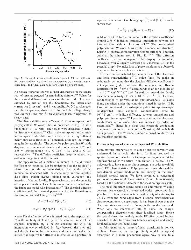
polycrystalline W oxide films is presented in Fig. 13 as a
function of Li+/W ratio. The results were discussed in detail
by Strømme Mattsson.338 Clearly the amorphous and crystal-
line samples exhibit diffusion coefficients with very different
behaviours as a function of potential, although the overall
magnitudes are similar. The curve for polycrystalline W oxide
displays two minima at steady state potentials of 2.75 and
2.55 V (corresponding to x # 0.03 ¡ 0.01 and x # 0.3,
respectively).339 The diffusion coefficient drops by almost two
orders of magnitude at the minima.
The appearance of a distinct minimum in the diffusion
coefficient vs. potential can be understood as the result of a
phase transition during intercalation. The depths of the
minima are associated with the crystallinity, and well-crystal-
lized films exhibit deeper minima upon extraction and
insertion of charge. Ideally, ~DD approaches zero as a discontinuity
at the phase transition. This phenomenon can be reconciled with
the lattice gas model with interactions.340 The chemical diffusion
coefficient and the chemical potential m for the Frumkin-type
isotherm in this model are given by340,341
~DD~U 1{Xð ÞX Lm=LXð Þ (10)
m = mu + Rgtln[X/(1 2 X)] + RgtgX (11)
where X is the fraction of ions inserted due to the step current,
U is the mobility at X = 0, mu is the standard value of the
chemical potential, Rg is the gas constant and g is the
interaction energy (divided by kBt) between the sites and
includes the Coulombic interaction and the strain field in the
lattice. g is negative for attractive interaction and positive for
repulsive interaction. Combining eqn (10) and (11), it can be
shown that
~DD~~DDX~0zg ~DDX ~0 1{Xð ÞX (12)
A fit of eqn (12) to the minimum in the diffusion coefficient
around 2.75 V indicated attractive interactions between the
inserted ions with g close to 24.338 The as-deposited
polycrystalline W oxide films exhibit a monoclinic structure.
During Li+ intercalation, they first become tetragonal and then
cubic at the minima seen in Fig. 12.339,342 The diffusion
coefficient for the amorphous film displays a smoother
behaviour with ~DD slightly decreasing as x increases (i.e., as the
potential drops). No indications of phase transitions are observed,
as expected for an amorphous structure.
This section is concluded by a comparison of the electronic
and ionic conductivities of W oxide films. We make an
estimate by assuming that the chemical diffusion coefficient is
not significantly different from the ionic one. A diffusion
coefficient of 10212 cm2 s21 corresponds to an ion mobility of
4 6 10211 cm2 V21 s21 and, for realistic intercalation levels,
an ionic conductivity of y3 6 1028 S cm21. The electronic
conductivities of polycrystalline and amorphous W oxide
films, deposited under the conditions stated in section II B,
have been measured by low-frequency dielectric spectroscopy.
As-deposited films exhibited conductivities close to
1027 S cm21, with little difference between amorphous and
polycrystalline samples.343 Upon intercalation, the electronic
conductance of W oxide films can increase by orders of
magnitude.310 Hence it is clear that electronic conduction
dominates over ionic conduction in W oxide, although both
are significant. Thus W oxide is indeed a mixed conductor, as
EC materials should be.
F. Concluding remarks on sputter deposited W oxide films
Many physical properties of W oxide films are currently well
understood. In particular this is so for films produced by
sputter deposition, which is a technique of major interest for
applications which we return to in section IV below. The W
oxide needs to have an amorphous structure in order to exhibit
good EC characteristics. Polycrystalline films also exhibit
considerable optical modulation, but mostly in the near-
infrared spectral region. We have presented a conceptual
picture of the structural characteristics of amorphous W oxide,
based on the notions of defects in the ideal amorphous state.
The most important recent results on amorphous W oxide
concern their electronic structure and optical properties. It is
possible to obtain the conduction band density of states (up to
2.5 eV from the band edge) from a simple electrochemical
chronopotentiometry experiment. It has been shown that the
electronic states are localized far up in the conduction band.
When ions are intercalated into W oxide, the charge-
compensating electrons enter these localized states. Hence
the optical absorption underlying the EC effect would be best
described as due to transitions between occupied and empty
localized conduction band states.
A fully quantitative theory of such transitions is not yet
at hand. However, one can profitably model the optical
absorption in a more phenomenological way as due to a
Fig. 13 Chemical diffusion coefficients from ref. 338 vs. Li/W ratio
for polycrystalline (pc; circles) and amorphous (a; squares) tungsten
oxide films. Individual data points are joined by straight lines.
138 | J. Mater. Chem., 2007, 17, 127–156 This journal is � The Royal Society of Chemistry 2007

superposition of possible transitions between the charge states
of the W ions (6+, 5+, and 4+). This model shows good
agreement with experiments in a very wide range of Li+
concentrations in the films and represents a major step
forward concerning a physical understanding of the optical
properties.
III. Nickel oxide films
The most commonly used anodic oxide-based EC materials are
Ni oxide344–347 and Ir oxide.348 They are able to change from a
transparent state to a neutral coloured one upon extraction of
protons or insertion of OH2 ions. Charge-balancing electrons
are simultaneously extracted from the valence band. The films
are probably a mixture of oxide and hydroxide components in
the bleached state, since a reservoir of protons seems to exist in
the films. Due to the high cost and limited supply of Ir, the use
of Ni oxide is favoured at least for large scale applications.
These materials have been less widely studied than W oxide.
However, the research has soared in recent years—especially
for Ni-oxide-based films—as seen from the references given in
the Introduction. Generally speaking, the physical under-
standing of the properties of anodic EC materials is on a less
advanced level than for W oxide (discussed in section II
above). Below we review the properties of Ni-oxide-based
materials with special emphasis on a recent thorough study in
the authors’ laboratory of Ni–V oxide thin films.349–351
A variety of mixed oxides have also been studied lately in an
attempt to improve the EC properties of anodically colouring
materials. A number of mixed Ni-based oxides with enhanced
modulation between the transparent and the coloured state
have been discovered.208–211 The optical properties of these
novel materials will be treated from a device perspective in
more detail in section IV. Intercalation of Li+ into Ni-oxide-
containing films has been researched several times,352–356 but it
seems that the optical properties are not modulated to any
large extent.357,358 This means that electrochromic Ni oxide
films only can be used in devices where the optical modulation
depends on proton/electron transport. One reason is that the
oxygen-rich compounds NiOOH and Ni2O3 are strongly
absorbing for visible light. It should be mentioned for
completeness that reversible charging and discharging under
Li+ exchange has been discovered recently; here it seems that
the Li+ insertion is accompanied by the formation of metallic
Ni dispersed in a matrix of Li2O.359
A. Structural features
The electrochromism in Ni-oxide-based materials probably
involves several Ni-containing phases. In this section we review
the basic properties of Ni oxides,360 hydroxides, and oxy-
hydroxides and how they can be transformed into one another
upon proton or OH2 exchange. In particular, we extend the
well established Bode reaction scheme361,362 to high levels of
proton exchange.
Nickel monoxide, NiO, exhibits a cubic NaCl structure with
a lattice parameter of 0.4173 nm.363 Single crystalline Ni
monoxide has a density of 6.67 g cm23.363 It is not possible to
make stoichiometric NiO crystals, since they always exhibit an
excess of oxygen.364 The extra oxygen cannot be placed inside
the NaCl structure; instead vacancies related to Ni2+ are
created, thus giving a p-type conduction character.365,366 A
schematic band diagram is depicted in Fig. 14 (after
Goodenough,262 Honig,263 and Hugel and Belkhir367). The
upper part of the valence band consists of Ni 3d states starting
at y2 eV below the Fermi level. In reality, these states overlap
with a wide O 2p band at y4 to 8 eV from the Fermi level;360
the Ni 3d and O 2p states are almost completely hybridized.368
There is a splitting between the Ni 3d levels with different spin
directions.367,369 The optical band gap is y4 eV;370 it may arise
from the separation between the minority spin t2g and eg
bands.369 The conduction band consists of unoccupied Ni 3d
(eg) states with an admixture of O 2p states; 4s and 4p bands
are present at higher energies.368,371
Ni hydroxide has a hexagonal structure that consists of a
packing of hydroxyl ions with Ni2+ occupying alternate rows
of octahedral sites.372 The Ni hydroxide exists in two
modifications, a and b. Their only difference is the quantity
of water needed for stabilization; the a phase occurs at low
content of water and the b phase at high content.373 The
Ni(OH)2 structure of the a form comprises a stacking of the
Ni(OH)2 layers with a large interlayer separation (y0.76 nm),
whereas the b-Ni(OH)2 has the same structure except that the
interlayer separation is much smaller (y0.46 nm).372 These
two phases can be further de-hydrated (oxidized) to the
corresponding c and b oxy-hydroxides for the a and b phases,
respectively, as proposed by Bode et al.361,362 The reaction
scheme is usually presented as
b-Ni OHð Þ2 < b-NiOOHzHzze{
? ?a-Ni OHð Þ2 < c-NiOOHzHzze{
(13)
Contraction is observed upon dehydration. A poorly crystal-
lized phase of Ni hydroxide, characterized by the coexistence
of a and b phases, has also been identified.374 The densities of
the pure phases differ considerably and have been reported to
be 2.6 to 2.8 g cm23 and 3.65 to 4.15 g cm23 for the a and b
Fig. 14 Schematic band structure of NiO, based on previous work in
refs. 262, 263, and 367. Nickel and oxygen orbitals as well as majority
and minority spin states are indicated using standard notation,
together with the Fermi level (eF). The indicated number of electrons
(e2) can be accommodated in the bands. Filled states are shaded.
This journal is � The Royal Society of Chemistry 2007 J. Mater. Chem., 2007, 17, 127–156 | 139

structures, respectively.361–363,375,376 An elucidation of the
Bode scheme has been given recently.377
Ni hydroxide is an n-type semiconductor with a band gap
of y3.6 to 3.9 eV, while the oxy-hydroxide phase is a p-type
semiconductor with a band gap of y1.7 to 1.8 eV.378
Additional absorption close to 1.5 eV has also been observed
for the Ni oxy-hydroxide.378 The electronic structure of the
hydroxide exhibits features similar to those of NiO, which is to
be expected since they have the same nature of the charge
transfer between Ni 3d and O 2p states.379
The Bode reaction scheme illustrated in reaction (13) above
does not involve NiO, and hence it cannot explain how nickel
in the NiO phase can change its valency from 2+ to 3+ upon
coloration. However, this reaction scheme can be extended in
order to include such a possibility.349,350 It is known that
excess oxygen in NiO produces a Ni2+ vacancy, which leads
to the creation of a hole on two adjacent Ni2+ ions, thus
producing Ni3+ ions.380 A similar situation is encountered
upon extraction of two protons from Ni hydroxide. The
condition of charge neutrality leads to the creation of two Ni3+
ions, and the superoxide Ni2O3 is formed from Ni oxide and
hydroxide. This reaction is included in the extended Bode
scheme in reaction (14) below, involving both proton extrac-
tion from the proton-containing Ni(OH)2 phase and valence
change of Ni atoms belonging to the NiO phase. The
extraction of H+ causes a transformation from Ni(OH)2 to
NiOOH, and the extraction of another H+ is compensated for
by creation of a hole on the Ni2+ in the NiO unit, viz.
b-Ni OHð Þ2��bleached
?
a-Ni OHð Þ2��bleached
< c-NiOOHjcolouredzHzze{
NiOza-Ni OHð Þ2��bleached
< Ni2O3jcolouredz2Hzz2e{
(14)
The compounds on the left-hand side are optically transparent,
while those on the right-hand side are absorbing. The
transformation from one to the other thus gives rise to the
characteristic electrochromism of hydrated Ni-oxide-based
materials.
Alternatively, OH2 groups may contribute to the ion
intercalation in Ni oxide and hydroxide according to the
reactions381,382
Ni(OH)2 + OH2 « NiOOH + H2O + e2 (15)
NiO + OH2 « NiOOH + e2 (16)
Indeed, some experimental evidence has been presented in
favour of this possibility.383 Below we will describe the results
of carefully designed experiments by which it is possible to
distinguish between H+ and OH2 exchange.
B. Thin film deposition
Magnetron sputtering has frequently been used for deposition
of Ni oxide coatings. DC and RF reactive sputtering
from metallic targets give films with similar properties, in
particular good electrochromism and good stability under
extended electrochemical cycling. Magnetron sputtering is an
industrially viable technique with excellent capacity for large
scale, large area manufacturing, but the magnetism of the Ni
target poses technical problems and it is more advantageous
to deposit Ni-oxide-based films from non-magnetic targets.
A widely available non-magnetic alloy is nickel–vanadium
containing 7% V. In order to ensure the technological
relevance of the present Feature Article, we concentrate below
on the properties of hydrated Ni–V oxide coatings produced
by sputtering. However, it should be noted that the deposition
process and the physical properties are similar to those of pure
Ni oxide as well as other Ni-oxide-based films. In particular,
the optical properties and the electrochromism of the Ni–V
oxide films are close to those of pure Ni oxide.
A non-magnetic Ni(93%)–V(7%) alloy was hence used as
sputter target. The deposition was conducted in a reactive
atmosphere of Ar + O2 or Ar + O2 + H2 onto ITO-coated
unheated glass substrates. The gas pressure was typically
30 mTorr and the film thickness was y200 nm. The deposition
process could be characterized by three regions;209,210,349 they
are depicted in Fig. 15, showing film deposition rate r and
luminous transmittance Tlum as a function of O2/Ar ratio. Tlum
was obtained by averaging the spectral transmittance over
the sensitivity of the human eye. At low oxygen content,
corresponding to region (1), films with close-to-metallic
reflectance were deposited. In region (2), the films were
transparent with Tlum being as high as 74%. Finally, dark
brown films were deposited at high oxygen content, corre-
sponding to region (3). Films from region (2) possess the best
EC properties. From a sputtering point of view, regions (1),
(2), and (3) correspond to metallic, partly oxidised, and
completely oxidised target surfaces, respectively. A stable set
point for thin film production was found to occur just before
the abrupt change in the deposition rate from region (2) to (3).
In region (3), the target tends to oxidise after a long period
of sputtering. The deposition rate can be increased by
applying a higher power to the target, since the quantity of
sputtered metal then increases. In this case, the curves in Fig. 15
will shift to the right, as the quantity of oxygen needed to
deposit the oxide must increase in order to equilibrate the
excess of metal.
Fig. 15 Deposition rate and luminous transmittance in the as-
deposited state of Ni–V oxide vs. O2 content in the sputtering
atmosphere. Three intervals are indicated corresponding to nearly
metallic (1), transparent (2), and dark brown (3) films. The thickness
was y200 nm for all films. Arrows indicate the applicable vertical
scale.
140 | J. Mater. Chem., 2007, 17, 127–156 This journal is � The Royal Society of Chemistry 2007

Addition of H2 to the gas mixture lowers r and increases the
transmittance in the as-deposited state by approximately 10%.
The films are brown at high hydrogen content (above 16%);
this probably follows from the lower deposition rate, implying
that more oxygen atoms per metal arrive at the substrate.
Optimum EC performance was observed at a low (2 to 12%)
amount of H2 in the gas mixture.
The percentage values of O2 and H2 in the gas mixture are
relative numbers and depend on the characteristics of the
equipment and the target. In general, the optimum relative
amounts of these gases correspond to a value just before the
target is oxidized and a decrease in the sputter rate is observed.
In the case of sputtering from a pure Ni target, for example,
the optimum O2/Ar ratio in region (2) is approximately 4.7%.
Elemental compositions were determined by Rutherford
backscattering spectrometry (RBS). However, the hydrogen
content could not be determined with this method. Defining
the composition as Ni12pVpOq, the three regions in Fig. 15
correspond to p # 0.11 and q ¡ 0.71 for region (1), 0.05 ¡
p ¡ 0.10 and 1.45 ¡ q ¡ 1.75 for region (2), and p # 0.11 and
q # 2.07 for region (3). As pointed out before, films with
optimum electrochromism were found in region (2); the
densities of the films with good EC properties were y3.6
to 4.2 g cm23.
The hydrated Ni–V oxide films on ITO were used as
working electrodes in a three-electrode electrochemical cell.
Specifically, the electrolyte was a 1 M KOH solution and the
film was cycled between 20.65 V and 0.65 V vs. an Ag/AgCl
reference electrode. The Ni–V oxide films had to be run
through 10 to 20 colour–bleach cycles before the inserted and
extracted charge became completely reversible. The stabilized
films were then taken out in their fully bleached and coloured
states in order to carry out ex-situ X-ray diffraction and other
physical measurements.
X-Ray diffraction was used to study the structure of as-
deposited and electrochemically coloured and bleached films
deposited under the conditions of region (2). Clear evidence
was found for a nano-crystalline phase. The diffraction
patterns were characteristic of cubic Ni oxide (bunsenite),
and the grain sizes were estimated to lie in the 10 to 25 nm
range. As-deposited and electrochemically cycled films showed
the same structural characteristics. No evidence was found for
crystalline phases containing vanadium or hydrogen. A recent
study384 based on EXAFS provided clear evidence that V ions
substitute Ni ions in the NiO-type structure and are distributed
without clear evidence for clustering. In transparent films the
V ions are at the centres of oxygen octahedra, and they shift by
about 0.04 nm to off-centre positions upon coloration.384
C. Electronic bandstructure
The electronic bandstructure of NiO has been extensively
studied by a number of computational and experimental
techniques; early work has been summarized several
times.365,369,385 Computations are cumbersome and often
controversial. However, significant advances have been made
and many experimental results can now be reproduced by
ab initio calculations.386–388 The electronic structure of
non-stoichiometric Ni oxide has also been studied recently,389
but its relevance for the electrochromic hydrated material is
not clear.
Ni-oxide-based EC films colour under proton extraction or
OH2 insertion. Charge compensating electrons are simulta-
neously extracted from the valence band of the compound. In
order to provide a deeper insight into the underlying science, it
is hence of much interest to detect changes in the occupied
electronic states during the exchange of ions. One of the most
convenient techniques to study the occupied states is XPS, as
noted in section II. Chronopotentiometry cannot be used in
the case of Ni-based oxides, because any information on the
electronic states would be obscured by a number of phase
transitions as protons are extracted. We return to these phase
transitions in section III E below. The present section reviews
a recent thorough XPS study of Ni–V oxide thin films by
Avendano et al.351 The films were prepared by sputter
deposition under conditions of region (2), as described above.
Data were taken by use of synchrotron radiation; the photon
energy was varied from 50 to 1500 eV. The end of the beam
line was equipped with a high-resolution hemispherical
electron analyser with an energy resolution E/DE from 103 to
104. The photon flux on the sample was in the range of 1011 to
1013 s21. Measured spectra were normalized with respect to the
Ni 2p core states, and the binding energy (BE) calibration was
done by setting the BE of adventitious carbon to 285 eV.390
XPS measurements were carried out for core states of Ni, O,
and V, as well as for the states forming the top of the valence
band. The measurements were performed on as-deposited,
bleached, and coloured hydrated Ni–V oxide films. The
measurements for the coloured and bleached conditions were
performed during the same run, on different halves of the same
film. We first discuss the core state spectra, since they contain
important information on the phases and compounds present
in the films.
Ni 2p3/2 states in NiO exhibit a double peak at BEs between
852 and 860 eV. For a perfect NiO crystal, the ratio between
the lower BE peak (centred at y854.8 eV) and the higher BE
peak (centred at y856.1 eV) is 4/3.391 Ni atoms in the 3+
valency state give an XPS peak centred at y855.7 eV, i.e.,
between the two peaks of the NiO. In the measured XPS
signal, the contribution of the 3+ states causes the double peak
to appear with an intensity ratio different than 4/3. The two
peaks overlap strongly in the spectra, but the change in the
peak shape is consistent with more Ni3+ ions in the coloured
film than in the bleached one.
The O 1s states in oxide phases such as NiO and Ni2O3
exhibit single peaks centred at y529.7 eV (refs. 391 and 392)
and 531.4 eV,393 respectively. In the hydrogen-containing
phases based on Ni(OH)2 and NiOOH, the O 1s peak is
located at y531.3 eV (refs. 394–396) and 531.7 eV,397
respectively. All of these peaks overlap in the measured
spectra, but the intensity redistribution within the measured
line can be used to obtain evidence for phase transformations
taking place upon coloration and bleaching.
Fig. 16 shows O 1s states for stabilised hydrated Ni-oxide-
based films in the coloured and bleached conditions. Spectra
were taken with two incident photon energies. Spectra for
the bleached film are consistent with a mixture of optically
transparent NiO and Ni(OH)2 phases. The spectra of the
This journal is � The Royal Society of Chemistry 2007 J. Mater. Chem., 2007, 17, 127–156 | 141

coloured film must have additional contributions from
NiOOH and/or Ni2O3, but these overlap with the Ni hydroxide
signal at y531.5 eV. However, it is observed that the NiO
peak at 529.7 eV decreases in intensity during coloration, while
the other peak increases. This clearly indicates that the NiO
phase plays a role in the coloration process. All of the spectra
in Fig. 16 have higher intensity at 758 eV than at 1061 eV. The
analyzed surface layer is thinner at lower photon energy;
therefore the results imply that the outermost surfaces of the
grains are more oxygen-rich than the bulk. Approximately
35% more oxygen was detected at the photon energy 758 eV
than at 1061 eV.
The O/Ni ratio at the surface was calculated by subtraction
of the XPS background and subsequent integration of the
spectra for the Ni 2p states, divided by the corresponding
values obtained for the O 1s states. The O/Ni ratio for as-
deposited films increased by y9% after five colour–bleach
cycles. In addition, for as-deposited films the peak at lower BE
(529.7 eV) was stronger than the other one. The reduction in
intensity upon going from the as-deposited to the stabilized
bleached condition can be attributed to transformation of the
hydrated Ni oxide to hydroxide. Such a transformation may
involve excess oxygen, present in the films from the beginning,
together with protons and/or OH2 introduced during electro-
chemical cycling.
For the stabilized films, the difference between the O/Ni
ratio for the bleached and coloured conditions was less than
1%, implying that there was no significant transport of oxygen
upon cycling. This result is important since it disproves the
interchange of hydroxyl groups during coloration and points
at intercalation of protons being the only important process.
Hence reaction (14), where NiO reacts with the hydroxide and
produces Ni2O3 upon proton extraction, is fully consistent
with the spectra presented in Fig. 16.
Fig. 17 shows the top of the valence band for stabilized
hydrated Ni–V oxide films under coloured and bleached
conditions. The valence band consists of Ni 3d states close to
the band edge together with a broad O 2p band at y2 to 6 eV
from the edge. In addition, a satellite can be seen at y10 eV.
The position of the Ni 3d peak is shifted by y0.6 eV towards
higher energy for the coloured film, as compared to its location
in the bleached one. A depopulation of the valence band in the
coloured state with respect to the bleached state is observed,
indicative of a valence change from 2+ to 3+ upon coloration.
Interestingly, no significant shift of the band edge could be
observed, and the decrease of the occupied electron states takes
place over a very broad energy range. The reason for these
features is not known at present. We note finally that valence
changes in the vanadium additive are possible in principle, but
ongoing work of ours shows beyond doubt that they play a
very insignificant role in the electrochromism.
D. Optical properties
The EC properties of Ni–V oxide films are strongly affected by
the amount of O2 in the sputter plasma. The nearly metallic
films, deposited with sputter parameters in region (1), did not
exhibit any optical modulation. The initially transparent films
in region (2), however, displayed pronounced electrochromism
with a bleached-state value of Tlum exceeding 80% and a
coloured-state transmittance strongly decreasing within a
narrow range of O2 flow. An increase of the O2 content of
the sputtering gas in this intermediate range also yielded a
significant enhancement of the charge capacity. Optimum
performance was found at O2 concentrations somewhat below
1.5%, as seen in Fig. 15. Larger O2 flows—corresponding to
region (3)—led to as-deposited absorbing films with weak
optical modulation and decreased charge capacity.
Transmittance and reflectance spectra were recorded for as-
deposited, coloured, and bleached films. Data for the coloured
and bleached films were obtained at maximum reversible
optical contrast. The absorption coefficient a(E) was calcu-
lated from T(E) and R(E) using eqn (6). Data for bleached and
coloured films are shown in Fig. 18. The optical spectra
resemble earlier ones for Ni oxide.53,346,347 Spectra for the
bleached film did not exhibit any structure in the studied
energy range. The absorption above 3.7 eV is due to the ITO
Fig. 17 XPS spectra for Ni 3d and O 2p states of stabilized hydrated
Ni–V oxide films in coloured and bleached conditions. The V 3d and
Ni 3d states are overlapping. A photon energy of 150 eV, with energy
pass of 10 eV and energy step 0.1 eV, was used.
Fig. 16 XPS spectra for O 1s core states of stabilized hydrated Ni–V
oxide films in coloured and bleached conditions. Photon energies of
1061 eV and 758 eV, with energy pass of 40 eV and energy step 0.1 eV,
were used.
142 | J. Mater. Chem., 2007, 17, 127–156 This journal is � The Royal Society of Chemistry 2007

base layer. By plotting ln(a) vs. photon energy one obtains a
linear dependence between 3.5 and 3 eV for the bleached film.
This behaviour is referred to as an Urbach tail;398 it is due to
excitations between localized states in the band gap and the
band edges. Logarithmic band edges have been reported399,400
before for hydrated V pentoxide, and hence the Urbach tail
in the Ni–V oxide films may be due to states associated with
the V ions.
The coloured film exhibited broad absorption from 1.5 to
3.7 eV. The increase of the absorption in the coloured film is
caused by charge transfer from Ni2+ to Ni3+ produced during
the extraction of protons, as discussed in section III C.
Previous results401 on films made by sputtering showed more
pronounced structure in the absorption spectra, associated
with oxygen excess in the Ni oxide. The inset in Fig. 18 shows
the absorption coefficient extracted from the present optical
spectra after subtraction of a base line.
The NiO phase is polycrystalline, and it is therefore
interesting to compare the optical absorption with the polaron
theory that was so successful in the case of polycrystalline W
oxide. For Ni oxide, most of the pertinent parameters can be
obtained from the literature. Thus e‘ = 5.4, e0 = 12, and ELO =
0.076 eV.402 In addition m/me is 1.66 (longitudinal) and 0.68
(transverse) in the valence band.325 These values lead to a
polaron coupling constant in the range of 1.1 to 1.75 and to a
polaron binding energy of the order of only 0.02 eV. The
predicted peak absorption would then overlap with the
longitudinal optical phonons far out in the infrared range. It
is probable that the absorbing Ni oxy-hydroxide—conceivably
being very disordered—gives the main contribution to the
optical absorption in Fig. 18.
In the infrared range, electrochromic Ni–V oxide films
exhibit strong phonon absorption both in the bleached and the
coloured states, although the details differ.350 The absence of a
significant free-electron component suggests that the states in
the valence band in Fig. 17 are actually localized. Hence the
optical absorption in Fig. 18 might be modelled, more
appropriately, on a premise of transitions between localized
states. It should be noted that the absorption peak is situated
in the region where the contributions of charge transfer
absorption from Ni2+ to Ni3+ have been predicted.401 We
return to the optical properties of Ni-oxide-based films, from a
device perspective, in section IV A below.
Coloration efficiency (CE) is a convenient parameter for
comparing the performance of EC films, as emphasized in
section II D where this parameter was defined. The CE is very
high for Ni-oxide-based films sputter deposited under condi-
tions corresponding to region (2). Spectral CE is depicted in
Fig. 19 for a hydrated Ni–V oxide film as well as for a similar
film coated by a thin Pd layer. This top layer serves as a
membrane that only allows H+ to penetrate to the underlying
film.403 Thus all other ions—such as OH2 and K+—were
filtered out. It should be noted, for completeness, that the Pd
layer did not display any optical modulation in the pertinent
voltage range. The difference in the magnitude of the CEs in
Fig. 19 ensues from the additional absorption in the Pd
coating. The wavelengths where the CE displays peaks are the
same in the cases of Pd coated and uncoated films. A decrease
of the CE towards increasing wavelengths can be observed in
both cases. The similarities in the main features of the CEs for
Pd coated and uncoated films strongly suggest that the
modulation of the optical absorption in the Ni-oxide-based
film is exclusively due to the insertion/extraction of hydrogen.
E. Ion diffusion
Ion transport properties were investigated by the GITT
technique337 applied to films of Ni–V oxide and pure Ni oxide
deposited under conditions of region (2).350 Prior to the GITT
measurement, all films were stabilized by having undergone
70 colour–bleach cycles in 1 M KOH. Specifically, the
sequential current steps in GITT were 0.08, 0.16, 0.24, 0.32,
and 0.40 mA, in cycles of nine; the currents were applied for
20 s, and the voltage was recorded during a relaxation time of
3580 s; the steady-state voltage was taken to be the one when
the change was less than 0.08 mV during 10 s.
We first compare the ion transport in hydrated Ni–V oxide
and Ni oxide films in order to study the possible influence of
the V on the electrochemical properties. Fig. 20 presents data
on chemical diffusion coefficient and quasi-steady-state
voltage (SSV) for a pure hydrated Ni oxide film made by
sputtering from a magnetic target of 99.9% Ni in an
atmosphere of Ar + O2 + H2. Data for a Ni–V oxide film,
deposited at the same power and pressure, are shown in Fig. 21.
In both cases it is seen that ~DD exhibits two deep minima at about
20.1 and 0.23 V. The SSV displays plateaus at these potentials,
although the relation of SSV to the extracted H+/Ni ratio exhibits
Fig. 19 Spectral coloration efficiency for Ni–V oxide films. The curve
for the film coated by a 25 nm thick layer of Pd (solid line) is multiplied
by a factor of two.
Fig. 18 Absorption coefficient vs. photon energy in the visible and
near-infrared regions for coloured and bleached Ni–V oxide films. The
inset shows extracted data on the broad peak in the coloured state.
This journal is � The Royal Society of Chemistry 2007 J. Mater. Chem., 2007, 17, 127–156 | 143

differences. It seems that the hydrated Ni oxide film contains more
hydrogen in the bleached state than the hydrated Ni–V oxide film.
The similarities between the data reported in Fig. 20 and 21
show that, effectively, the minima for ~DD ensue solely from the
base material, i.e., the hydrous Ni oxide. We next interpret the two
well-defined plateaus at 20.1 and 0.23 V which in both cases
correspond to distinct minima in ~DD. The appearance of a sharp
minimum in the diffusion coefficient vs. potential can be under-
stood as the result of a phase transition340—as pointed out in
section II E above—in the present case occurring during the
extraction of protons from the hydrated Ni-oxide-based films. The
amplitude of the minima of ~DD is associated with the crystallinity,
and well-crystallized films exhibit deep minima upon extraction
and insertion of charge. It is possible to identify the phases
involved in the de-intercalation process by comparing the
potentials at which the minima of ~DD appear with the optical
properties. At the first minimum the film is still transparent, but
the second one is located where the absorption starts to rise.
We suggest that the first minimum in Fig. 20 and 21
corresponds to the transition from b-Ni hydroxide to a-Ni
hydroxide, and that the second one stems from a transition
from a-Ni hydroxide to c-Ni oxy-hydroxide. It is well known
that the Ni oxy-hydroxide phases have higher absorption
than the Ni hydroxide phases.53 The proposed phase transi-
tions only involve proton exchange, which in the case under
study is the dominating process governing the coloration. The
assignment is fully consistent with the Bode reaction scheme
given in section III A.
Accurate measurements of the initial quantity of hydrogen
in the films are not available, and hence it is only possible to
make a qualitative analysis of the data presented in Fig. 20 and
21. At the two apparent phase changes, ~DD decreases by four to
five orders of magnitude at the actual transition. This means that
the model of the Frumkin-type isotherm that was introduced in
section II E—in which the electron exchange is slow enough that
quasi-equilibrium conditions may be assumed—is an excellent
approach for a qualitative analysis.341 When ~DD approaches zero at
the phase change, the ‘‘critical’’ value of g will be close to 24,
which means that the net force between the ions is attractive.341
We finally consider the electronic conductivity of electro-
chromic Ni oxide. Bleached films exhibit very low conduc-
tivity, of the order of 10211 S cm21, but the conductivity
increases rapidly as the Ni oxide is coloured.404 Under deep
coloration, the electronic conductivity is of the same order of
magnitude as for as-deposited W oxide. Ni oxide is hence
a mixed conductor, but with a much lower electronic
conductivity than for W oxide.
F. Concluding remarks on sputter deposited Ni–V oxide films
There is an excess of oxygen in the as-deposited films, in
combination with low density (high porosity) and small grain
size. The grain surface is richer in oxygen than the bulk.
Independently of the colour, there are always Ni atoms in
valence states 2+ and 3+ in the films. The number of Ni3+ ions
increases upon coloration.
A NiO structure was found by X-ray diffraction for films in
all colour conditions, while the presence of other Ni-based
phases—such as Ni(OH)2, Ni2O3, and NiOOH—was inferred
from other data. This indicates that the coloration process is a
surface phenomenon, most likely occurring in the outer parts
of the grains.
In the beginning of an electrochemical cycling sequence, a
number of cycles are required for the charge capacity to reach
its maximum value and stabilize. XPS results are consistent
with a transformation of the over-stoichiometric hydrated Ni
oxide to hydroxide and oxy-hydroxide phases on the grain
surfaces. The amount of oxygen in the films increases by
y25% by intercalation of OH2 groups occurring simulta-
neously with intercalation of protons from the electrolyte.
GITT results350 suggest crystallization of the hydroxide and
oxy-hydroxide phases during the initial intercalation cycles.
After the charge capacity has been stabilized, experiments with
Pd coated films, together with XPS results, showed that the
electrochemical coloration occurs solely by proton intercala-
tion, with the oxygen content in the films being equal under
bleached and coloured conditions.
Upon proton extraction, GITT measurements were con-
sistent with the Bode scheme in reaction (13). However, the
Bode model does not explain the 2+ to 3+ valence change
for nickel belonging to the NiO phase upon coloration, as
observed by XPS (Fig. 16). An extension of the Bode scheme
was suggested to account for these results; see section III B.
Approximately three monolayers have been estimated as the
depth resolution for the Ni 2p and O 1s core levels when the
Fig. 20 Chemical diffusion coefficient of H+ vs. steady-state voltage
(SSV) (a) and SSV vs. atomic fraction of hydrogen (with respect to Ni)
(b) deintercalated from an optimized Ni oxide film.
Fig. 21 Chemical diffusion coefficient of H+ vs. steady-state voltage
(SSV) (a) and SSV vs. atomic fraction of hydrogen (with respect to Ni)
(b) deintercalated from an optimized Ni–V oxide film. Pertinent
experimental parameters are given in the main text.
144 | J. Mater. Chem., 2007, 17, 127–156 This journal is � The Royal Society of Chemistry 2007

photon energy is 1061 eV. Because the coloration is a surface
effect and the bulk remains NiO independently of the film
being bleached or coloured, one can argue that—after the
transformation of the Ni(OH)2 to NiOOH—the change of the
NiO to Ni2O3 may take place at the interface between the NiO
and the Ni oxy-hydroxide. Owing to the fact that the
electrochromism is basically a surface phenomenon, there is
also a possibility that surface-related states—such as those for
oxygen-reduced NiO(1 0 0)—lead to optical absorption due to
in-gap states, which in this case appear to be related to surface
metallicity.405
IV. Devices based on tungsten oxide and nickel oxide
After having examined the fundamental properties of W
oxide and Ni oxide films in sections II and III, respectively, we
turn to devices incorporating such films. Rigid, glass-based
devices of this kind have been reported on in a number of
studies,66,195,406–417 and recently work on flexible polyester-
film-based devices has been carried out in the authors’
laboratory.70,418–420 Devices for emittance control have been
discussed as well.417,421–424
With regard to device-related aspects, we first note that
an optimization of the bleached-state transmittance and the
colour rendering are of very great importance for practical
applications, especially in the field of architecture.425,426 W
oxide films are able to attain a highly transparent state, and the
mixing with other oxides, such as Mo oxide and V oxide, is
well known to produce a more or less neutral colour.53,137 The
colour properties of Ni-oxide-based EC films have received
less interest until a recent comprehensive investigation was
done by Avendano et al.211 (which expanded some earlier
work208). The results of this investigation are summarized in
section IV A below. Colour properties of Au-containing Ni
oxide films have received some attention as well.192 The colour
of electrochromic Ir-oxide-based films has attracted interest
recently too.157,427 Below we also cover aspects of device
manufacturing with regard to thin film deposition and pre-
assembly charge balancing in section IV B and device assembly
and initial tests in section IV C.
A. Optical properties of Ni-oxide-based films: bleached-state
transmittance and colour
Films of Ni-based oxides were deposited using standard DC
and RF reactive magnetron co-sputtering from targets of
Mg, Al, Si, Ni, Zr, Nb, Ag, Ta, Ni(61.5%)–Al(38.5%), and
Ni(93%)–V(7%), following procedures outlined in section III B
and described in detail by Avendano et al.209,211,428 Unheated
glass substrates, pre-coated with ITO having a resistance of
60 V square21, were used for optical and electrochemical
investigations as before, whereas polished carbon substrates
were used for compositional analysis using RBS. Atomic ratios
Mg/Ni = 0.80 and Al/Ni = 0.59 ¡ 0.03 led to optimized EC
properties.211 These compositions correspond to non-magnetic
or weakly-magnetic sputter targets, which is advantageous
with regard to manufacturing. The Ni–Mg-oxide-based system
has been studied in detail, and it appears that NipMg12pO as
well as NipMg12p(OH)2 form solid solutions as a consequence
of the similarities of the ionic radii for Ni2+ and Mg2+.429–431
Cyclic voltammograms were recorded by use of a three-
electrode electrochemical cell in a 1 M KOH solution. After
some initial voltammetric cycles to stabilize the EC perfor-
mance, spectral transmittance T(l) and reflectance R(l) were
measured in the 300 , l , 800 nm range with the films in their
fully bleached and coloured states. In general, the shapes of the
voltammograms changed depending on the specific additive to
Ni oxide, but the main features characteristic of the pure
oxide tended to prevail. The charge capacity—and hence the
magnitude of the electrochromism—is influenced by the
potentiodynamic range, particularly the potential for full
coloration, Ecol. Similar charge capacities (from 15 to
20 mC cm22) could be obtained provided that Ecol was varied
by 0.05 to 0.1 V when additives were present. This shift is
insignificant for EC device applications.
It is of particular interest to be able to maximize the
bleached-state transmittance in EC devices, as pointed out
above. To that end we evaluated the spectral absorptance A(l)
for Ni-oxide-based films from A(l) = 1 2 T(l) 2 R(l). Fig. 22
shows that a significant decrease of A(l) occurred at short
wavelengths for additives Mg, Al, Si, Zr, Nb, and Ta, whereas
films containing V or Ag did not show any improvement in
their optical properties compared to those of pure Ni oxide.
Similar results for Mg additives have been reported also by
others.432 The addition of Fe or Zn makes the band gap
smaller.433,434 The increase of the bleached-state transmittance
did not have any detrimental effect on the coloration
efficiency. In fact, a CE even somewhat larger than that
shown for Ni–V oxide in Fig. 19 could be observed for Ni–Al
oxide films.211
Fig. 22 Spectral absorptance of electrochromic Ni-oxide-based films
in their bleached states. The designation NiMO (with M being Mg, Al,
Si, V, Zr, Nb, Ag, or Ta) indicates that M is present in the oxide but
does not specify the amount.
This journal is � The Royal Society of Chemistry 2007 J. Mater. Chem., 2007, 17, 127–156 | 145

The strong absorptance at l , 350 nm is due to the
semiconductor band gap, which appears to be widened as a
consequence of the addition of Mg, Al, Si, Zr, Nb, or Ta and
narrowed by the addition of V or Ag. Alternatively, the
additives may affect optical absorption caused by defects
such as vacancies, over-stoichiometry, grain boundaries, etc.
Thermodynamically stable Ni oxide is a p-type conductor
due to excess oxygen365,366 as pointed out in section III A. It is
then plausible that the p-type conductivity and the residual
optical absorption in the bleached state originate from the
same electron states, and this may explain why films of pure Ni
oxide cannot be made completely colourless. When Al is
added, for example, it can act as a donor of electrons and
fill electron (hole) states, thereby reducing the residual
absorption. The addition of V, on the other hand, may
provide acceptor states whose effect would be to enhance the
residual absorption.
We next consider the colour of electrochromic Ni-oxide-
based films. Quantitative assessments of colour can be
performed in several different ways; here we employ the CIE
colorimetric system.435,436 The purpose of colorimetric analysis
is to give colour specifications for observers with normal vision
in terms of tri-stimulus values or chromaticity coordinates.
The ideal observer’s colour matching functions are denoted
x,y, and z, and represent red, green, and blue primaries,
respectively. One can describe any colour as an additive
mixture of these. The y curve is chosen so that it coincides
with the luminous efficiency of the light-adapted eye, and
hence it can be used to evaluate Tlum. The CIE 1964 tri-
stimulus values corresponding to a certain colour stimulus
Y(l) are obtained from
XCIE~
Ð�XX lð ÞY lð ÞdlÐ
�YY lð ÞS lð Þdl(17)
and analogously for YCIE and ZCIE. The colour stimulus of
present interest is Y(l) = S(l)T(l) where S(l) is the relative
spectral irradiance function. Chromaticity coordinates—
denoted x, y, and z—are then obtained from
x = XCIE/(XCIE + YCIE + ZCIE) (18)
and correspondingly for y and z. These formulae lead to
the chromaticity diagram shown in the lower parts of
the various panels of Fig. 23. Any colour can be
represented as a point within the shown boundary. The
chromaticity coordinates for a colourless (achromatic) mate-
rial are x = y = z = 0.333.
The chromaticity coordinates were calculated for four
different standard illuminants representing a chosen set of
light sources. Illuminant D65 signifies the average North sky
daylight at 6500 K, illuminant A represents a tungsten halogen
incandescent light source at 2856 K (typical home or store
accent lighting), illuminant F11 pertains to a commercial rare-
earth-phosphor narrow-band fluorescent light source at 4000 K
(used in Europe and the Pacific Rim for typical office or store
lighting), and illuminant F2 represents a commercial wide-
band-fluorescent cool white light source at 4150 K (typical
office or store lighting in the USA).
Fig. 23 shows chromaticity coordinates for the optimized
Ni-oxide-based thin films reported on in Fig. 22 under CIE
standard illuminants D65, A, F11, and F2. For illuminant
D65, the data pertaining to the bleached state lie very close
to the point representing colourlessness. The data for the
coloured state are rather scattered, with the chromaticity
depending on the specific additive. Also the trajectories in
colour space between the bleached and coloured states are
different for each of the additives. Another characteristic of
the bleached state is that the dominant wavelengths are
short so that the eye has low sensitivity. The chromaticity
coordinates for the incandescent light (illuminant A) indicate a
light yellow colour in the bleached state and a yellow–green
colour in the dark state. The data points for the bleached state
appear less dispersed than the corresponding points for D65.
For fluorescent lights, F11 for narrow-band fluorescent and
F2 for cool white fluorescent light sources, the data are similar
Fig. 23 CIE chromaticity diagrams representing the colour of
optimized electrochromic Ni-oxide-based films in fully bleached and
coloured states under daylight illumination (CIE D65), incandescent
illumination (CIE A), narrow-band fluorescent illumination (CIE
F11), and cool white fluorescent illumination (CIE F2). Coordinates
signifying the illuminant as well as colourlessness (i.e., the achromatic
point) are plotted as references. The upper part of each panel is a
magnification of the central region of the lower part. The designation
NiMO (with M being Mg, Al, Si, V, Zr, Nb, or Ta) indicates that M is
present in the oxide but does not specify the amount.
146 | J. Mater. Chem., 2007, 17, 127–156 This journal is � The Royal Society of Chemistry 2007

and dispersed as regards the coloured states. The films show a
green–yellow colour in the bleached state.
Fig. 24 shows YCIE, which corresponds to the luminous
transmittance. The results are entirely consistent with those in
Fig. 22. Films of Ni oxide mixed with Mg and Al show a Tlum
as large as 85%, whereas films containing Si and Zr yield Tlums
up to y83%. For additives of Nb or Ta, Tlum can be y80%.
The case of the V admixture is different, though, and shows
that Tlum does not exceed 75%, i.e., lying y4% below the
value for pure Ni oxide. Generally speaking, the luminous
transmittance shows a rather weak dependence on the specific
illuminant.
B. Deposition and pre-assembly charge balancing
This section reports on a new flexible EC foil device with
sufficient optical modulation range, dynamics, and durability
for practical uses.70 The device embodies a film of W oxide
made by sputtering in the presence of hydrogen, another film
of Ni–V oxide made by sputtering and post-deposition
treatment in ozone, and a polymer laminate.
DC magnetron sputtering was performed as reported in
sections II B and III B. The substrates were of 0.175 mm thick
polyester (PET) pre-coated with ITO typically having a
resistance per square of 60 V. Substrates were roughly 30 610 cm2 in size. Sputtering took place in Ar + O2 + H2 with
optimized mixing ratio as before.
From a manufacturing point of view, it is preferable to be
able to deposit the films under conditions that make them
ready for device lamination, or to have convenient processes
for making the as-deposited films ready for this. In the case of
W oxide, it is possible to carry out the deposition in Ar + O2 +
H2 according to principles delineated by Giri and Messier.437
The hydrogen produces a blue colour for the as-deposited
films, and the key issue with regard to optimizing the gas
mixture is to incorporate hydrogen into the film without
creating oxygen deficiency.
In practice, the optimization of the W oxide films can be
made by measuring their colour in the as-deposited state.
Fig. 25 compares the chromaticity coordinate z, corresponding
to blue light,436 with the variation of the luminous transmit-
tance for films deposited in Ar + O2 and Ar + O2 + H2. Data
for a ‘‘standard’’ film deposited in Ar + O2 and coloured
electrochemically by Li+ incorporation are shown as a
reference. As-deposited films, produced in Ar + O2, displayed
a decrease in transmittance when the O2 partial pressure was
lowered. It can be seen from Fig. 25 that these under-oxidized
films exhibit a colour that is very different from the one in the
electrochemically coloured films. When sputtering was done in
Ar + O2 + H2, however, the transmittance of the as-deposited
films was decreased when the H2 partial pressure was
increased. Such films showed the same colour rendering as
the electrochemically treated films for transmittance levels
down to about 20% in 300 nm thick films. The evolution of z at
still lower transmittance levels is most likely associated with
oxygen deficiency. Fig. 26 illustrates the spectral transmittance
for a film that is ready for integration in a device.
The Ni–V oxide films are transparent in the as-deposited
state and require pre-treatment prior to device lamination.
Charge insertion via an electrochemical procedure is possible,
in principle, but obviously unwieldy and not suited for
practical fabrication. An alternative method for charging was
Fig. 25 Chromaticity coordinate z, corresponding to blue light, vs.
luminous transmittance for 300 nm thick tungsten oxide films of three
types: deposited in Ar + O2 and then coloured by charge insertion from
an electrolyte of LiCiO4 in propylene carbonate (PC), as deposited in
Ar + O2 with different oxygen contents, and as deposited in Ar + O2 +
H2 with different hydrogen contents. The colour specifications were
made by integration of spectrophotometrically recorded transmittance.
Symbols denote evaluated data and lines were drawn for convenience.
Fig. 26 Spectral transmittance of a 300 nm thick tungsten oxide film
produced by sputtering in Ar + O2 + H2 under conditions making it
ready for device lamination.
Fig. 24 Luminous transmittance YCIE (equal to Tlum) for the
Ni-oxide-based films reported on in Fig. 23 exposed to four different
CIE standard illuminants. The designation NiMO (with M being Mg,
Al, Si, V, Zr, Nb, or Ta) indicates that M is present in the oxide but
does not specify the amount.
This journal is � The Royal Society of Chemistry 2007 J. Mater. Chem., 2007, 17, 127–156 | 147

developed recently by Azens et al.438 Essentially, this new
method employs exposure to ozone obtained by ultraviolet
irradiation of the film in the presence of oxygen. The reaction
paths involved in ozone treatment have been discussed
recently.439 Fig. 27 displays the decrease of the luminous
transmittance as a function of time when a conventional ozone
photo-reactor was used to treat a 220 nm thick Ni–V oxide
film. The transmittance drops by some 50% during a few
minutes, and a further decrease takes place for extended
exposure times. Fig. 28 illustrates the typical spectral
transmittance for a Ni–V oxide film prior to device lamination.
C. Device assembly and initial tests
Polyester-based foils—one with a W oxide film coloured by
sputtering in the presence of H2 (cf. Fig. 26) and another with a
Ni–V oxide film coloured by post-deposition ozone exposure
(cf. Fig. 28)—were laminated together by a PMMA-based
electrolyte related to the type described by Wixwat et al.440
using roll-pressing at 80 uC. The edges of the double foil were
then sealed, electrical contacts were attached, and the EC
device was ready for testing and use. Cycling between coloured
and bleached states took place using trapezoidal voltage pulses
between 21.6 and +1.5 V, respectively. The precise voltage
range was adjusted automatically to compensate for varying
temperatures.
Fig. 29 shows the transmittance at three different wave-
lengths for cycling with one full colour–bleach cycle each 200 s.
The optical modulation is pronounced, especially for mid-
luminous and red light. Most of the changes take place within
a few tens of seconds after application of the pulse, but the
coloration has not reached saturation even after several
minutes. Fig. 30 reports on the transmittance in fully coloured
and bleached states after cycling in the same way as in Fig. 29.
The foils are seen to switch between a high level of about
70% and a low level of 35 to 40% at a mid-luminous
wavelength, which is in agreement with the data in Fig. 29.
The span between the coloured and bleached states is shown
to remain practically unchanged for 5000 cycles. This by
no means represents the maximum achievable number of
cycles, though. Lower transmittance levels, down to 25%
or less in the coloured state, could be reached for longer
coloration times.
The devices have open-circuit memory, which is an asset
since electrical power must be drawn only to effect changes in
the optical properties. Fig. 31 illustrates the mid-luminous
transmittance for a device coloured to a transmittance equal to
20%. It is found that the transmittance has increased only
marginally after a time as long as 160 h.
Fig. 29 Transmittance at three wavelengths vs. time for electrochro-
mic switching of a laminated device as described in the main text.
Fig. 30 Transmittance at a wavelength of 550 nm vs. number of
colour–bleach cycles for a laminated electrochromic foil device in
coloured and bleached states.
Fig. 27 Luminous transmittance vs. post-deposition ozone exposure
time for 220 nm thick Ni–V oxide films produced by sputtering in
Ar + O2 + H2.
Fig. 28 Spectral transmittance of a 220 nm thick Ni–V oxide film
produced by sputtering in Ar + O2 + H2 and post-treated in ozone
under conditions making it ready for device lamination.
148 | J. Mater. Chem., 2007, 17, 127–156 This journal is � The Royal Society of Chemistry 2007

V. Some applications aspects
The work reported in section IV above demonstrated
techniques to produce EC devices—in particular flexible EC
foils—with sufficient optical modulation range, dynamics, and
durability for making them interesting with regard to a
number of important applications. The largest and most
challenging of these, and also probably the most difficult one,
is ‘‘smart’’ windows5 for uses in buildings and automobiles.
Detailed technical information on practical EC devices is
rarely found in the literature; however, some examples of
devices were reported in recent work by Kubo et al.441,442 and
Schutt et al.443 and a computational feasibility study for EC
windows in vehicles was presented by Jaksic and Salahifar.14 It
is important to realize that the ‘‘smart’’ windows can fulfil
different goals: they can provide improved indoor comfort by
being able to prevent glare and thermal discomfort for the
users of the building or automobile, and simultaneously they
can provide large energy savings through a lowered cost for air
cooling; they are therefore perfectly in tune with the notion of
‘‘intelligent buildings’’.444 Specifically, EC foils may be of
much interest for membrane architecture445,446 by being able
to regulate energy flows and lighting in large constructions
with very little embedded energy. The ‘‘smart’’ windows
technology is thus able to yield environmental benefits, and
in this context it is important to have environmental
assessments regarding EC glazing production, as reported
recently by Syrrakou et al.447 Economics aspects of the
technology have been modeled448 as well as diverse applica-
tions issues449–451 including net energy performance of EC
skylights.9
The order of magnitude of the energy savings possible with
‘‘smart’’ windows technology is considered next, following
previous work at the authors’ laboratory.8,10,11 The solar
energy falling onto a vertical surface per year is set to
1000 kWh m22. This can serve as a nominal value, whereas
more correct numbers for South-facing/North-facing/horizon-
tal surfaces are 850/350/920, 1400/450/1700, and 1100/560/
1800 kWh m22 for Stockholm (Sweden), Denver (USA), and
Miami (USA), respectively. Half of this, 500 kWh m22, is
visible light. This number is used below since infrared
radiation can be reflected off—at least in principle—by use
of known technology that does not require variable transmit-
tance. If the transparency can be altered between 7 and 75%—
which is by no means unlikely given further electrochromics
technology development—the difference between having the
window constantly coloured and constantly bleached is
340 kWh m22. The stated range of optical modulation can
be accomplished already today, but at the expense of slow
dynamics and some degradation.10,11 The next issue is then to
contemplate when the ‘‘smart’’ window should be coloured
and when it should be bleached. With physical presence as the
overriding control strategy, the question is when a room is in
use—or, more precisely, the fraction of the solar energy that
enters when nobody is present. Considering that a normal
(office) room is empty during vacations, holidays and week-
ends, early mornings and late afternoons (when the sun is
near the horizon), etc., it is surely a conservative estimate
that 50% of the energy enters the room when there is no one
to look through the window. Hence this estimate yields that
170 kWh m22 is the amount of energy saved annually by
adopting the given control strategy.
Is this energy savings significant or not? To answer this
question, we note that 17% is a typical value for today’s best
thin-film solar cells and sub-modules.452 Thus these solar cells
would be able to generate 170 kWh m22 in the example given
above. Of course the analogy between energy savings in
‘‘smart’’ windows and energy generation in solar cells is
not tied to the choice of the incident solar energy being
1000 kWh m22 but applies generally irrespective of the
orientation of the surface under examination. The ‘‘smart’’
window saves thermal energy, but if the cooling machine—
operating with an efficiency of 300%, say—runs on electricity
generated with an efficiency of 33% then the analogy becomes
perfect. This latter consideration implies that one employs a
‘‘national scenario’’ for the energy, with a ‘‘Coefficient-of-
Performance’’ (‘‘COP-factor’’) equal to unity.
Building simulations were carried out recently with the
object of providing realistic estimates of the energy savings
inherent in the ‘‘smart’’ windows technology. Initial results are
presently being published by Roos et al.453,454 Specifically,
calculations for a standard office module with well defined
size, window area, lighting demand, occupancy, equipment,
etc., showed that the energy savings potential was considerable
for the cooling load. The studied office block was oriented
with one facade facing South and one facing North and the
simulations were performed with climate data applicable to
Rome (Italy), Brussels (Belgium), and Stockholm (Sweden).
When using ‘‘smart’’ windows instead of conventional static
solar control windows, the energy for space cooling, on an
annual basis, could be reduced by as much as 40 to 50%. The
amount of saved energy is obviously climate dependent. In
moderately warm climates, such as Brussels and Stockholm,
the number of days with very high outdoor temperature is
relatively small but the energy required for balancing excessive
solar energy inflow nevertheless is substantial, and an
interesting result of the simulations was that the cooling
power could be reduced so that air conditioning may be
completely avoided when ‘‘smart’’ windows were used. In this
Fig. 31 Transmittance at a wavelength of 550 nm vs. time for a
laminated electrochromic foil device kept under open-circuit
conditions.
This journal is � The Royal Society of Chemistry 2007 J. Mater. Chem., 2007, 17, 127–156 | 149

case, the additional cost for ‘‘smart’’ windows can be more
than compensated for by the elimination of an air conditioning
system. The method for controlling the ‘‘smart’’ windows is of
obvious importance and has been the subject of some recent
studies.455–462
Potential applications in energy efficient buildings and
automobiles have provided the main impetus for research
and development on electrochromics for several years.
However, there are numerous other applications as well,
especially with regard to foil-type EC devices. These can be
applied, for example, in ski goggles and visors for motorcycle
helmets. These visors can be coloured to a chosen degree in
the day and bleached in the night. It is especially important
that the driving and riding safety can be significantly improved
by having the visor bleach before entering tunnels or other
dark spaces. Another aspect with a bearing on safety is that
facial warming can be significantly limited by absorption in
the visor.463
Acknowledgements
Many persons have contributed to the results presented in this
Feature Article. In particular we wish to thank Drs Lars
Berggren and Esteban Avendano for their dedicated work as
Ph.D. students; their results form the bases of much of sections
II and III, respectively. Dr Andris Azens contributed, in
particular, to many of the results reported in section IV.
References
1 Large-Area Chromogenics: Materials and Devices for Trans-mittance Control, ed. C. M. Lampert and C. G. Granqvist,SPIE Opt. Eng. Press, Bellingham, USA, 1990, vol. IS4.
2 S. K. Deb, Appl. Opt., Suppl., 1969, 3, 192.3 S. K. Deb, Philos. Mag., 1973, 27, 801.4 J. S. E. M. Svensson and C. G. Granqvist, Sol. Energy Mater.,
1984, 11, 29.5 J. S. E. M. Svensson and C. G. Granqvist, Sol. Energy Mater.,
1985, 12, 391.6 C. G. Granqvist, Adv. Mater., 2003, 15, 1789.7 C. G. Granqvist, in Encyclopedia of Energy, ed. C. J. Cleveland,
Elsevier, Oxford, UK, 2004, vol. 3, p. 845.8 C. G. Granqvist, Int. Glass Rev., 2001, (2), 67.9 J. H. Klems, Energy Build., 2001, 33, 93.
10 C. G. Granqvist, Smart Mater. Bull., 2002, (10), 9.11 A. Azens and C. G. Granqvist, J. Solid State Electrochem., 2003,
7, 64.12 M. R. LaPointe and G. M. Sottile, Proc. Soc. Photo-Opt. Instrum.
Eng., 2001, 4458, 112.13 G. M. Sottile, Mater. Sci. Eng., B, 2005, 119, 240.14 N. I. Jaksic and C. Salahifar, Sol. Energy Mater. Sol. Cells, 2003,
79, 409.15 T. Sumida, Y. Wada, T. Kitamura and S. Yanagida, Chem. Lett.,
2002, 31, 180.16 S.-L. Kuai, G. Bader and P. V. Ashrit, Appl. Phys. Lett., 2005, 86,
221110.17 N. Kobayashi, M. Nishimura and H. Ohtomo, Electrochim. Acta,
2005, 50, 3886.18 N. Kobayashi and M. Nishimura, Sol. Energy Mater. Sol. Cells,
2006, 90, 538.19 A. A. Argun, P.-H. Aubert, B. C. Thompson, I. Schwendeman,
C. L. Gaupp, J. Hwang, N. J. Pinto, D. B. Tanner,A. G. MacDiarmid and J. R. Reynolds, Chem. Mater., 2004,16, 4401.
20 H. J. Byker, Electrochim. Acta, 2001, 46, 2015.21 U. Bach, D. Corr, D. Lupo, F. Pichot and M. Ryan, Adv. Mater.,
2002, 14, 845.
22 H. Pettersson, T. Gruszecki, L.-H. Johansson, M. O. M. Edwards,A. Hagfeldt and T. Matuszczyk, Displays, 2004, 25, 223.
23 H. Hagenstrom, in Proc. 4th Int. Conf. on Coatings on Glass, ed.C.-P. Klages, H. J. Glaser and M. A. Aegerter, Fraunhofer-Institut fur Schicht- und Oberflachentechnik, Braunschweig,Germany, 2002, p. 21.
24 C. M. Lampert, Sol. Energy Mater. Sol. Cells, 2003, 76, 489.25 C. M. Lampert, Mater. Today, 2004, (3), 28.26 S. C. de Oliveira, L. C. de Morais, A. A. da Silva Curvelo and
R. M. Torresi, J. Electrochem. Soc., 2003, 150, E578.27 J. Isidorsson, I. A. M. E. Giebels, E. S. Kooji, N. J. Koeman,
J. H. Rector, A. T. M. van Gogh and R. Griessen, Electrochim.Acta, 2001, 46, 2179.
28 A.-M. Janner, P. van der Sluis and V. Mercier, Electrochim. Acta,2001, 46, 2173.
29 P. van der Sluis and V. M. M. Mercier, Electrochim. Acta, 2001,46, 2167.
30 B. Farangis, P. Nachimuthu, T. J. Richardson, J. L. Slack,B. K. Meyer, R. C. C. Perera and M. D. Rubin, Solid State Ionics,2003, 165, 309.
31 T. J. Richardson, Solid State Ionics, 2003, 165, 305.32 I. Aruna, B. R. Mehta, L. K. Malhotra and S. M. Shivaprasad,
Adv. Mater., 2004, 16, 169.33 I. A. M. E. Giebels, J. Isidorsson and R. Griessen, Phys. Rev. B,
2004, 69, 205111.34 E. Johansson, C. Chacon, C. Zlotea, Y. Andersson and
B. Hjorvarsson, J. Phys.: Condens. Matter, 2004, 16, 7649.35 W. Lohstroh, R. J. Westerwaal, B. Noheda, S. Enache,
I. A. M. E. Giebels, B. Dam and R. Griessen, Phys. Rev. Lett.,2004, 93, 197404.
36 J. L. M. van Mechtelen, B. Noheda, W. Lohstroh, R. J.Westerwaal, J. H. Rector, B. Dam and R. Griessen, Appl. Phys.Lett., 2004, 84, 3651.
37 S. Enache, T. Leeuwerink, A. F. Th. Hoekstra, A. Remhof,N. J. Koeman, B. Dam and R. Griessen, J. Alloys Compd., 2005,397, 9.
38 C. G. Granqvist, in Materials Science for Solar Energy ConversionSystems, ed. C. G. Granqvist, Pergamon, Oxford, UK, 1991,p. 106.
39 C. G. Granqvist and A. Hultaker, Thin Solid Films, 2002, 411, 1.40 D. S. Ginley and C. Bright, MRS Bull., 2000, 25(8), 15.41 P. P. Edwards, A. Porsch, M. O. Jones, D. V. Morgan and
R. M. Perks, Dalton Trans., 2004, (19), 2995.42 T. Minami, Semicond. Sci. Technol., 2005, 20, S35.43 J. Lu, A. Hultaker, G. A. Niklasson, C. G. Granqvist and
E. Olsson, Thin Solid Films, 2005, 479, 107.44 Y. Furubayashi, T. Hitosugi, Y. Yamamoto, K. Inaba,
G. Kinoda, Y. Hirose, T. Shimada and T. Hasegawa, Appl.Phys. Lett., 2005, 86, 252101.
45 G. Leftheriotis, S. Papaefthimiou and P. Yanoulis, Sol. EnergyMater. Sol. Cells, 2000, 61, 107.
46 S. Papaefthimiou, G. Leftheriotis and P. Yanoulis, Electrochim.Acta, 2001, 46, 2145.
47 Z.-C. Wu, Z.-H. Chen, X. Du, J. M. Logan, J. Sippel, M. Nikolou,K. Kamaras, J. R. Reynolds, D. B. Tanner, A. F. Hebard andA. G. Rinzler, Science, 2004, 305, 1273.
48 C. Marcel and J.-M. Tarascon, Solid State Ionics, 2001, 143, 89.49 L.-C. Chen, Y.-H. Huang, K.-S. Tseng and K.-C. Ho, J. New
Mater. Electrochem. Syst., 2002, 5, 203.50 L.-C. Chen, K.-S. Tseng, Y.-H. Huang and K.-C. Ho, J. New
Mater. Electrochem. Syst., 2002, 5, 213.51 K.-H. Heckner and A. Kraft, Solid State Ionics, 2002, 152–153,
899.52 P. Knauth and H. L. Tuller, J. Am. Ceram. Soc., 2002, 85, 1654.53 C. G. Granqvist, Handbook of Inorganic Electrochromic
Materials, Elsevier, Amsterdam, The Netherlands, 1995, reprinted2002.
54 P. M. S. Monk, R. J. Mortimer and D. R. Rosseinsky,Electrochromism: Fundamentals and Applications, VCH,Weinheim, Germany, 1995.
55 P. R. Somani and S. Radhakrishnan, Mater. Chem. Phys., 2002,77, 117.
56 C. G. Granqvist, Sol. Energy Mater. Sol. Cells, 2000, 60, 201.57 C. G. Granqvist, E. Avendano and A. Azens, Thin Solid Films,
2003, 442, 201.
150 | J. Mater. Chem., 2007, 17, 127–156 This journal is � The Royal Society of Chemistry 2007
58 P. Losier and P. V. Ashrit, J. Mater. Sci. Lett., 2003, 22, 1095.59 A. Lusis, J. Kleperis and E. Pentjuss, J. Solid State Electrochem.,
2003, 7, 106.60 E. Ozkan, S.-H. Lee, C. E. Tracy, J. R. Pitts and S. K. Deb, Sol.
Energy Mater. Sol. Cells, 2003, 79, 439.61 J. Garcıa-Canadas, I. Mora-Sero, F. Fabregat-Santiago,
J. Bisquert and G. Garcia-Belmonte, J. Electroanal. Chem.,2004, 565, 329.
62 J. Garcıa-Canadas, F. Fabregat-Santiago, I. Porqueras, C. Person,J. Bisquert and G. Garcia-Belmonte, Solid State Ionics, 2004, 175,521.
63 A. Siokou, S. Ntais, S. Papaefthimiou, G. Leftheriotis andP. Yianoulis, Surf. Sci., 2004, 566–568, 1168.
64 R. Sivakumar, M. Jayachandran and C. Sanjeeviraja, Mater.Chem. Phys., 2004, 87, 439.
65 H. Qiu, Y. F. Lu and Z. H. Mai, J. Appl. Phys., 2002, 91, 440.66 K.-S. Ahn, Y.-C. Nah, Y.-E. Sung, K.-Y. Cho, S.-S. Shin and
J.-K. Park, Appl. Phys. Lett., 2002, 81, 3930.67 Y.-S. Huang, Y.-Z. Zhang, Z.-T. Zeng and X.-F. Hu, Appl. Surf.
Sci., 2002, 202, 104.68 W. J. Lee, Y. K. Fang, J.-J. Ho, C.-Y. Chen, S.-F. Chen,
R.-Y. Tsai, D. Huang and F. C. Ho, J. Mater. Sci.: Mater.Electron., 2002, 13, 751.
69 F. van Driel, F. Decker, F. Simone and A. Pennisi, J. Electroanal.Chem., 2002, 537, 125.
70 A. Azens, G. Gustavsson, R. Karmhag and C. G. Granqvist,Solid State Ionics, 2003, 165, 1.
71 L. Berggren and G. A. Niklasson, Solid State Ionics, 2003, 165,51.
72 F.-P. Dai, S.-Y. Lu, B.-X. Feng, S.-R. Jiang and C. Chen, ActaPhys. Sin., 2003, 52, 1003.
73 Y.-C. Nah, K.-S. Ahn and Y.-E. Sung, Solid State Ionics, 2003,165, 229.
74 J. Scarminio, Sol. Energy Mater. Sol. Cells, 2003, 79, 357.75 E. Washizu, A. Yamamoto, Y. Abe, M. Kawamura and
K. Sasaki, Solid State Ionics, 2003, 165, 175.76 H.-N. Cui, S. Jia, L.-J. Meng and V. Texeira, Microchim. Acta,
2004, 145, 19.77 H. Kamal, A. A. Akl and K. Abdel-Hady, Physica B, 2004, 349,
192.78 E. Avendano, L. Berggren, G. A. Niklasson, C. G. Granqvist and
A. Azens, Thin Solid Films, 2006, 496, 30.79 L. Berggren and G. A. Niklasson, Sol. Energy Mater. Sol. Cells,
2005, 85, 573.80 K. W. Park, Electrochim. Acta, 2005, 50, 4690.81 H. Sadiki, J. F. Pierson, C. Rousselot, N. Martin and
G. Terwagne, Surf. Coating Technol., 2005, 200, 232.82 M. Stolze, D. Gogova and L.-K. Thomas, Thin Solid Films, 2005,
476, 185.83 T.-S. Yang, Z.-R. Lin and M.-S. Wong, Appl. Surf. Sci., to be
published.84 S. J. Yoo, J. W. Lim and Y.-E. Sung, Sol. Energy Mater. Sol.
Cells, 2006, 90, 477.85 L. Meda, R. C. Breitkopf, T. E. Haas and R. U. Kirss, Thin Solid
Films, 2002, 402, 126.86 K. Gesheva, A. Szekeres and T. Ivanova, Sol. Energy Mater. Sol.
Cells, 2003, 76, 563.87 J. Scarminio, M. A. Bica de Moraes, R. C. E. Dias, F. P. Rouxinol
and S. F. Durrant, Electrochem. Solid-State Lett., 2003, 6, H9.88 C. S. Blackman and I. P. Parkin, Chem. Mater., 2005, 17, 1583.89 Z. Dimitrova and D. Gogova, Mater. Res. Bull., 2005, 40, 333.90 F. Hamelmann, K. Gesheva, T. Ivanova, A. Szekeres,
M. Abrashev and U. Heinzmann, J. Optoelectron. Adv. Mater.,2005, 7, 393.
91 M. Seman and C. A. Wolden, J. Vac. Sci. Technol., A, 2003, 21,1927.
92 M. Seman and C. A. Wolden, Sol. Energy Mater. Sol. Cells, 2004,82, 517.
93 P. S. Patil, J. Solid State Electrochem., 2002, 6, 284.94 M. Regragui, M. Addou, A. Outzourhit, E. El Idrissi,
A. Kachouane and A. Bougrine, Sol. Energy Mater. Sol. Cells,2003, 77, 341.
95 R. Sivakumar, A. M. E. Raj, B. Subramanian, M. Jayachandran,D. C. Trivendi and C. Sanjeeviraja, Mater. Res. Bull., 2004, 39,1479.
96 C. O. Avellaneda, K. Dahmouche and L. O. S. Bulhoes, Mol.Cryst. Liq. Cryst., 2002, 374, 113.
97 A. Hauch, A. Georg, U. Opara Krasovec and B. Orel,J. Electrochem. Soc., 2002, 149, H159.
98 U. Opara Krasovec, A. Surca Vuk and B. Orel, Sol. EnergyMater. Sol. Cells, 2002, 73, 21.
99 E. Ozkan, S.-H. Lee, P. Liu, C. E. Tracy, F. Z. Tepehan, J. R. Pittsand S. K. Deb, Solid State Ionics, 2002, 149, 139.
100 P. Varshney, M. Deepa, N. Sharma and S. A. Agnihotry, SolidState Ionics, 2002, 152–153, 877.
101 C. O. Avellaneda and L. O. S. Bulhoes, Solid State Ionics, 2003,165, 59.
102 C. O. Avellaneda and L. O. S. Bulhoes, J. Solid StateElectrochem., 2003, 7, 183.
103 S. Badilescu and P. V. Ashrit, Solid State Ionics, 2003, 158, 187.104 P. K. Biswas, N. C. Pramanik, M. K. Mahapatra, D. Ganguli and
J. Livage, Mater. Lett., 2003, 57, 4429.105 P. R. Bueno, R. C. Faria, C. O. Avellaneda, E. R. Leite and
L. O. S. Bulhoes, Solid State Ionics, 2003, 158, 415.106 Y. Djaoued, P. V. Ashrit, S. Badilescu and R. Bruning, Proc. Soc.
Photo-Opt. Instrum. Eng., 2003, 5123, 202.107 B. Orel, A. Surca Vuk, R. Jese, P. Lianos, E. Stathatos,
P. Judeinstein and Ph. Colomban, Solid State Ionics, 2003, 165,235.
108 D. L. Sun, S. Heusing, J. Puetz and M. A. Aegerter, Solid StateIonics, 2003, 165, 181.
109 A. Surca Vuk, B. Orel, H. Spreizer and P. Colomban, Solid StateIonics, 2003, 165, 247.
110 A. Surca Vuk, B. Orel and P. Colomban, Acta Chim. Slov., 2003,50, 601.
111 I. Turyan, B. Orel, R. Reisfeld and D. Mandler, Phys. Chem.Chem. Phys., 2003, 5, 3212.
112 A. Cremonesi, D. Bersani, P. P. Lottici, Y. Djaoued andP. V. Ashrit, J. Non-Cryst. Solids, 2004, 345&346, 500.
113 G. Garcia-Belmonte, P. R. Bueno and F. Fabregat-Santiago,J. Appl. Phys., 2004, 96, 853.
114 G. Leftheriotis, S. Papaefthimiou and P. Yanoulis, Sol. EnergyMater. Sol. Cells, 2004, 83, 115.
115 A. Patra, K. Auddy, D. Ganguli, J. Livage and P. K. Biswas,Mater. Lett., 2004, 58, 1059.
116 A. Pawlicka, D. C. Dragunski, K. V. Guimaraes andC. O. Avellaneda, Mol. Cryst. Liq. Cryst., 2004, 416, 105.
117 R. Solarska, B. D. Alexander and J. Augustynski, J. Solid StateElectrochem., 2004, 8, 748.
118 S. A. Agnihotry, R. Sharma, M. Kar and T. K. Saxena, Sol.Energy Mater. Sol. Cells, 2006, 90, 15.
119 C. O. Avellaneda and L. O. S. Bulhoes, Sol. Energy Mater. Sol.Cells, 2006, 90, 395.
120 M. Deepa, R. Sharma, A. Basu and S. A. Agnihotry, Electrochim.Acta, 2005, 50, 3545.
121 F. Huguenin, E. R. Gonzalez and O. N. Oliveira, Jr., J. Phys.Chem. B, 2005, 109, 12837.
122 A. Novinrooz, M. Sharbatdaran and H. Noorkojouri, Cent. Eur.J. Phys., 2005, 3, 456.
123 A. K. Srivastava, M. Deepa, S. Singh, R. Kishore andS. A. Agnihotry, Solid State Ionics, 2005, 176, 1161.
124 T. Pauporte, J. Electrochem. Soc., 2002, 149, C539.125 R. Vijayalakshmi, M. Jayachandran and C. Sanjeeviraja, Curr.
Appl. Phys., 2003, 3, 171.126 M. Deepa, M. Kar and S. A. Agnihotry, Thin Solid Films, 2004,
468, 32.127 Yu. S. Krasnov and G. Ya. Kolbasov, Electrochim. Acta, 2004,
49, 2425.128 T. Pauporte, M. C. Bernard, Y. Soldo-Olivier and R. Faure,
J. Electrochem. Soc., 2004, 151, H21.129 M. Deepa, A. K. Srivastava, T. K. Saxena and S. A. Agnihotry,
Appl. Surf. Sci., 2005, 252, 1568.130 A. Kraft, M. Rottmann and K.-H. Heckner, Sol. Energy Mater.
Sol. Cells, 2006, 90, 469.131 G. A. Tsirlina, K. Miecznikowski, P. J. Kuleza, M. I. Borzenko,
A. N. Gavrilov, L. M. Plyasova and I. Yu. Molina, Solid StateIonics, 2005, 176, 1681.
132 T. Ivanova, K. A. Gesheva, M. Ganchev and E. Tzvetkova,J. Mater Sci.: Mater. Electron., 2003, 14, 755.
This journal is � The Royal Society of Chemistry 2007 J. Mater. Chem., 2007, 17, 127–156 | 151

133 T. Ivanova, K. Gesheva, F. Hamelmann, G. Popkirov,M. Abrashev, M. Ganchev and E. Tzvetkova, Vacuum, 2004,76, 195.
134 T. Ivanova, K. A. Gesheva, G. Popkirov, M. Ganchev andE. Tzvetkova, Mater. Sci. Eng., B, 2005, 119, 232.
135 S.-H. Baeck, T. F. Jaramillo, D. H. Jeong and E. W. McFarland,Chem. Commun., 2004, (4), 390.
136 K. R. Padmanabhan, Nucl. Instrum. Methods Phys. Res., Sect. B,2004, 219–220, 942.
137 A. Rougier, A. Blyr, J. Garcia, Q. Zhang and S. A. Impey, Sol.Energy Mater. Sol. Cells, 2002, 71, 343.
138 E. Pehlivan, F. Z. Tepehan and G. G. Tepehan, Solid State Ionics,2003, 165, 105.
139 D. Yang and L. Xue, Thin Solid Films, 2004, 469–470, 54.140 A. E. Aliev and H. W. Shin, Solid State Ionics, 2002, 154–155,
425.141 M. Yuan, Y. Lu, B. Tian, H. Yang, B. Tu, J. Kong and D. Zhao,
Chem. Lett., 2004, 33, 1396.142 P. S. Patil, S. H. Mujawar, A. I. Inamdar and S. B. Sadale, Appl.
Surf. Sci., 2005, 250, 117.143 N. R. de Tacconi, C. R. Chenthamrakshan, K. L. Wouters,
F. M. MacDonnell and K. Rajeshwar, J. Electroanal. Chem.,2004, 566, 249.
144 A. Medina, J. L. Solis, J. Rodriguez and W. Estrada, Sol. EnergyMater. Sol. Cells, 2004, 80, 473.
145 M. Yagi and S. Umemiya, J. Phys. Chem. B, 2002, 106, 6355.146 E. Ozkan Zayim, P. Liu, S.-H. Lee, C. E. Tracy, J. A. Turner,
J. R. Pitts and S. K. Deb, Solid State Ionics, 2003, 165, 65.147 M. Yagi, K. Sone, M. Yamada and S. Umemiya, Chem.–Eur. J.,
2005, 11, 767.148 Z. Hussain, J. Electron. Mater., 2002, 31, 615.149 Z. Hussain, J. Appl. Phys., 2002, 91, 5745.150 T. S. Sian, G. B. Reddy and S. M. Shivaprasad, Electrochem.
Solid-State Lett., 2005, 8, A96.151 S.-H. Lee, M. J. Seong, C. E. Tracy, A. Mascarenhas, J. R. Pitts
and S. K. Deb, Solid State Ionics, 2002, 147, 129.152 A. Taj and P. V. Ashrit, J. Mater. Sci., 2004, 39, 3541.153 T. Ivanova, K. A. Gesheva and A. Szekeres, J. Solid State
Electrochem., 2002, 7, 21.154 T. Ivanova, M. Surtchev and K. Gesheva, Mater. Lett., 2002, 53,
250.155 K. A. Gesheva, T. Ivanova, G. Popkirov and F. Hamelmann,
J. Optoelectron. Adv. Mater., 2005, 7, 169.156 T. M. McEvoy, K. J. Stevenson, J. T. Hupp and X.-J. Dang,
Langmuir, 2003, 19, 4316.157 A. Azens and C. G. Granqvist, Appl. Phys. Lett., 2002, 81, 928.158 P. S. Patil, R. K. Kawar and S. B. Sadale, Electrochim. Acta,
2005, 50, 2527.159 P. S. Patil, R. K. Kawar and S. B. Sadale, Appl. Surf. Sci., 2005,
49, 367.160 Y. Jung, J. Lee and Y. Tak, Electrochem. Solid-State Lett., 2004,
7, H5.161 J. Yano, K. Noguchi, S. Yamasaki and S. Yamasaki,
Electrochem. Commun., 2004, 6, 110.162 L. Sziraki and L. Bobics, Electrochim. Acta, 2002, 47, 2189.163 J. Backholm, A. Azens and G. A. Niklasson, Sol. Energy Mater
Sol. Cells, 2006, 90, 414.164 K. D. Lee, J. Korean Phys. Soc., 2005, 46, 1383.165 H. Tokudome and M. Miyauchi, Angew. Chem., Int. Ed., 2005,
44, 1974.166 F. Artuso, F. Decker, A. Krasilnikova, M. Liberatore,
A. Lourenco, E. Masetti, A. Pennisi and F. Simone, Chem.Mater., 2002, 14, 636.
167 M. Benmoussa, A. Outzourhit, A. Bennouna and E. L. Ameziane,Thin Solid Films, 2002, 405, 11.
168 L. Ottaviano, A. Pennisi, F. Simone and A. M. Salvi, Opt. Mater.,2004, 27, 307.
169 M. Seman, J. Marino, W. Yang and C. A. Wolden, J. Non-Cryst.Solids, 2005, 351, 1987.
170 C. O. Avellaneda and L. O. S. Bulhoes, Solar Energy Mater. SolarCells, 2006, 90, 444.
171 M. Benmoussa, A. Outzourhit, A. Bennouna and E. L. Ameziane,J. Phys. IV, 2005, 123, 41.
172 M. Liberatore, F. Decker, A. Surca Vuk, B. Orel and G. Drazic,Sol. Energy Mater. Sol. Cells, 2006, 90, 434.
173 P. Liu, S.-H. Lee, C. E. Tracy, J. A. Turner, J. R. Pitts andS. K. Deb, Solid State Ionics, 2003, 165, 223.
174 S. Neves, R. F. Santos, W. A. Gazotti and C. P. Fonseca, ThinSolid Films, 2004, 460, 300.
175 K. Takahashi, Y. Wang and G. Cao, Appl. Phys. Lett., 2005, 86,053102.
176 W. Chen and Y. Kaneko, J. Electroanal. Chem., 2003, 559, 83.177 Y. Kaneko, S. Mori and J. Yamanaka, Solid State Ionics, 2002,
151, 35.178 Y. Kaneko and W. Chen, J. Electroanal. Chem., 2003, 559, 87.179 C.-G. Wu and M.-H. Chung, J. Solid State Chem., 2004, 177,
2285.180 J. Verlevska and M. Ristova, Sol. Energy Mater. Sol. Cells, 2002,
73, 131.181 K. D. Lee and W. C. Jung, J. Korean Phys. Soc., 2004, 45, 447.182 I. Bouessay, A. Rougier, B. Beaudoin and J. B. Leriche, Appl.
Surf. Sci., 2002, 186, 490.183 I. Bouessay, A. Rougier and J.-M. Tarascon, J. Electrochem. Soc.,
2004, 151, H145.184 I. Bouessay, A. Rougier, P. Poizot, J. Moscovici, A. Michailowicz
and J.-M. Tarascon, Electrochim. Acta, 2005, 50, 3737.185 N. Penin, A. Rougier, L. Laffont, P. Poizot and J.-M. Tarascon,
Sol. Energy Mater. Sol. Cells, 2006, 90, 422.186 K.-S. Ahn, Y.-C. Nah and Y.-E. Sung, Jpn. J. Appl. Phys., 2002,
41, L533.187 K.-S. Ahn, Y.-C. Nah and Y.-E. Sung, J. Vac. Sci. Technol. A,
2002, 20, 1468.188 K.-S. Ahn, Y.-C. Nah and Y.-E. Sung, J. Appl. Phys., 2002, 92,
1268.189 K.-S. Ahn, Y.-C. Nah and Y.-E. Sung, J. Appl. Phys., 2002, 92,
7128.190 K.-S. Ahn, Y.-C. Nah and Y.-E. Sung, Appl. Surf. Sci., 2002, 199,
259.191 K.-S. Ahn, Y.-C. Nah, J.-H. Yum and Y.-E. Sung, Jpn. J. Appl.
Phys., 2002, 41, L212.192 M. C. A. Fantini, F. F. Ferreira and A. Gorenstein, Solid State
Ionics, 2002, 152–153, 867.193 S. R. Jiang, P. X. Yan, B. X. Feng, X. M. Cai and J. Wang,
Mater. Chem. Phys., 2002, 77, 384.194 Y.-Y. Shi, Z.-Y. Zhou and X.-O. Yang, Sol. Energy Mater. Sol.
Cells, 2002, 71, 51.195 K.-S. Ahn, Y.-C. Nah, J.-Y. Park, Y.-E. Sung, K.-Y. Cho,
S.-S. Shin and J.-K. Park, Appl. Phys. Lett., 2003, 82, 3379.196 K.-S. Ahn, Y.-C. Nah and Y.-E. Sung, Solid State Ionics, 2003,
156, 433.197 K.-S. Ahn, Y.-C. Nah and Y.-E. Sung, Solid State Ionics, 2003,
165, 155.198 F. Iwata, K. Mikage, H. Sakaguchi, M. Kitao and A. Sasaki,
Solid State Ionics, 2003, 165, 7.199 S.-H. Lee, C. E. Tracy and J. R. Pitts, Electrochem. Solid-State
Lett., 2004, 7, A299.200 C. R. Magana, D. R. Acosta, A. I. Martınez and J. M. Ortega,
Sol. Energy, 2006, 80, 161.201 S. A. Mahmoud, A. A. Akl, H. Kamal and K. Abdel-Hady,
Physica B, 2002, 311, 366.202 H. Kamal, E. K. Elmaghraby, S. A. Ali and K. Abdel-Hady, Thin
Solid Films, 2005, 483, 330.203 R. Cerc Korosec, P. Bukovec, B. Pihlar, A. Surca Vuk, B. Orel
and G. Drazic, Solid State Ionics, 2003, 165, 191.204 Z. Jiao, M.-H. Wu, Z. Qin and H. Xu, Nanotechnology, 2003, 14,
458.205 R. Cerc Korosec and P. Bukovec, Thermochim. Acta, 2004, 410, 65.206 L. Ottaviano, A. Pennisi and F. Simone, Surf. Interface Anal.,
2004, 36, 1335.207 K. Nakaoka, J. Ueyama and K. Ogura, J. Electroanal. Chem.,
2004, 571, 93.208 A. Azens, J. Isidorsson, R. Karmhag and C. G. Granqvist, Thin
Solid Films, 2002, 422, 1.209 E. Avendano, A. Azens, J. Isidorsson, R. Karmhag,
G. A. Niklasson and C. G. Granqvist, Solid State Ionics, 2003,165, 169.
210 E. Avendano, A. Azens, G. A. Niklasson and C. G. Granqvist,J. Solid State Electrochem., 2003, 8, 37.
211 E. Avendano, A. Azens, G. A. Niklasson and C. G. Granqvist,Sol. Energy Mater. Sol. Cells, 2004, 84, 337.
152 | J. Mater. Chem., 2007, 17, 127–156 This journal is � The Royal Society of Chemistry 2007

212 H.-J. Ahn, S.-S. Shim, Y.-S. Kim, C.-Y. Kim and T.-Y. Seong,Electrochem. Commun., 2005, 7, 567.
213 S.-H. Lee, E. Tracy, Y. Yan, J. R. Pitts and S. K. Deb,Electrochem. Solid-State Lett., 2005, 8, A188.
214 E. Avendano, A. Azens, G. A. Niklasson and C. G. Granqvist,Mater. Sci. Eng., B, to be published.
215 F. F. Ferreira and M. C. A. Fantini, Solid State Ionics, 2004, 175,517.
216 Z. He, Z. Ji, S. Zhao, C. Wang, K. Liu and Z. Ye, Sol. Energy,2006, 80, 226.
217 Y.-S. Huang, Y.-Z. Zhang and X.-F. Hu, Sol. Energy Mater. Sol.Cells, 2003, 77, 155.
218 M. A. Aegerter, M. Schmitt and Y. Guo, Int. J. Photoenergy,2002, 4, 1.
219 L. Melo, C. O. Avellaneda and A. Pawlicka, Mol. Cryst. Liq.Cryst., 2002, 374, 101.
220 A. V. Rosario and E. C. Pereira, Sol. Energy Mater. Sol. Cells,2002, 71, 41.
221 P. R. Bueno, R. C. Faria and L. O. S. Bulhoes, Solid State Ionics,2005, 176, 1175.
222 S. Heusing, D.-L. Sun, J. Otero-Anaya and M. A. Aegerter, ThinSolid Films, 2006, 502, 240.
223 H.-H. Wang, C.-J. Zhao, M.-M. Yan and Z.-Y. Jiang, Acta Chim.Sin., 2002, 60, 1203.
224 Y.-N. NuLi, Z.-W. Fu, Y.-Q. Chu and Q.-Z. Qin, Solid StateIonics, 2003, 160, 197.
225 K.-Y. Park and M. F. Toney, Electrochem. Commun., 2005, 7,151.
226 N. Naghavi, C. Marcel, L. Dupont, J.-B. Leriche andJ.-M. Tarascon, Solid State Ionics, 2003, 156, 463.
227 M. Pflughoefft and H. Weller, J. Phys. Chem. B, 2002, 106, 10530.228 L.-C. Chen, Y.-H. Huang and K.-C. Ho, J. Solid State
Electrochem., 2002, 7, 6.229 N. R. De Tacconi, K. Rajeshwar and R. O. Lezna, Chem. Mater.,
2003, 15, 3046.230 C. Salinga, H. Weis and M. Wuttig, Thin Solid Films, 2002, 414,
275.231 H. R. Wilson, R. Blessing, H. Hagenstrom, M. G. Hutchins,
D. Dvorjetski and W. J. Platzer, in Proc. 4th Int. Conf. on Coatingson Glass, ed. C.-P. Klages, H. J. Glaser and M. A. Aegerter,Fraunhofer-Institut fur Schicht- und Oberflachentechnik,Braunschweig, Germany, 2002, p. 649.
232 X. C. Xu, H. Shen and X. Y. Xiong, Thin Solid Films, 2002, 415,290.
233 A. Martucci, M. Pasquale, M. Guglielmi, M. Post and J. C. Pivin,J. Am. Ceram. Soc., 2003, 86, 1638.
234 J. Okumu, F. Koerfer, C. Salinga and M. Wuttig, J. Appl. Phys.,2004, 95, 7632.
235 H. Shanak, H. Schmitt, J. Nowoczin and C. Ziebert, Solid StateIonics, 2004, 171, 99.
236 H. Cheong, H. C. Jo, K. M. Kim and S.-H. Lee, J. Korean Phys.Soc., 2005, 46, S121.
237 J. Nowoczin, H. Shanak, C. Ziebert, H. Schmitt and K. H. Ehses,Phys. Status Solidi A, 2005, 202, 1073.
238 H. Shanak, H. Schmitt, J. Nowoczin and K.-H. Ehses, J. Mater.Sci., 2005, 40, 3467.
239 H.-S. Shim, H.-J. Ahn, T.-Y. Seong and K.-Y. Park, Electrochem.Solid-State Lett., 2005, 8, A277.
240 C. Alcomber, F. Alvarez, S. A. Bilmes and R. J. Candal, J. Mater.Sci. Lett., 2002, 21, 501.
241 W. Feng, T. R. Zhang, L. Wei, R. Lu, Y. B. Bai, T. J. Li,Y. Y. Zhao and J. N. Yao, Mater. Lett., 2002, 54, 309.
242 T. He, Y. Ma, Y. Cao, X. Hu, H. Liu, G. Zhang, W. Yang andJ. Yao, J. Phys. Chem. B, 2002, 106, 12670.
243 T. He, Y. Ma, Y. Cao, W. Yang and J. Yao, Phys. Chem. Chem.Phys., 2002, 4, 1637.
244 H. Ikake, Y. Fukuda, S. Shimizu, K. Kurita and S. Yano,Kobunshi Ronbunshu, 2002, 59, 608.
245 C. O. Avellaneda and L. O. S. Bulhoes, Solid State Ionics, 2003,165, 117.
246 Y. He, Z. Wu, L. Fu, C. Li, Y. Miao, L. Cao, H. Fan and B. Zou,Chem. Mater., 2003, 15, 4039.
247 R.-G. Xie, J.-Q. Zhuang, L.-L. Wang, W.-S. Yang, D.-J. Wang,T.-J. Li and J.-N. Yao, Chem. J. Chin. Univ., 2003, 24, 2086.
248 M. F. Al-Kuhaili, S. M. A. Durrani and E. E. Khawaja, ThinSolid Films, 2002, 408, 188.
249 S. M. A. Durrani, E. E. Khawaja, M. A. Salim, M. F. Al-Kuhailiand A. M. Al-Shukri, Sol. Energy Mater. Sol. Cells, 2002, 71, 313.
250 M. Merz, J. Eisenmenger, B. Heinz and P. Ziemann, Phys. Rev. B,2002, 66, 184102.
251 M. Miyakawa, K. Ueda and H. Hosono, J. Appl. Phys., 2002, 92,2017.
252 M. Miyauchi, A. Nakajima, T. Watanabe and K. Hashimoto,Chem. Mater., 2002, 14, 2812.
253 B. Canut, A. Merlen, V. Teodorescu, C. Ghica, C. S. Sandu,S. M. M. Ramos, C. Bovier, R. Espiau de la Maestre,A. Broniatowski and H. Bernas, Nucl. Instrum. Methods Phys.Res., Sect. B, 2003, 209, 335.
254 E. Ozkan Zayim and N. Dogan Baydogan, Sol. Energy Mater.Sol. Cells, 2006, 90, 402.
255 C. Wang, M. Shim and P. Guyot-Sionnest, Appl. Phys. Lett.,2002, 80, 4.
256 P. Guyot-Sionnest and C. Wang, J. Phys. Chem. B, 2003, 107,7355.
257 X.-S. Yang, Y. Wang, L. Dong and L.-Z. Qi, Acta Phys. Sin.,2004, 53, 2724.
258 X.-S. Yang, Y. Wang and Y. Zhao, Mater. Lett., to be published.259 H. Mizoguchi, M. Orita, M. Hirano, S. Fujitsu, T. Takeuchi and
H. Hosono, Appl. Phys. Lett., 2002, 80, 4732.260 P. M. S. Monk, Crit. Rev. Solid State Mater. Sci., 1999, 24, 193.261 G. A. Niklasson, L. Berggren and A.-L. Larsson, Sol. Energy
Mater. Sol. Cells, 2004, 84, 315.262 J. B. Goodenough, in Progress in Solid State Chemistry, ed.
H. Reiss, Pergamon, Oxford, UK, 1971, vol. 5, p. 145.263 J. M. Honig, in Electrodes of Conductive Metallic Oxides, ed.
S. Trasatti, Elsevier, Amsterdam, The Netherlands, 1980, p. 2.264 A.-L. Larsson, B. E. Sernelius and G. A. Niklasson, Solid State
Ionics, 2003, 165, 35.265 R. B. Goldner, D. H. Mendelsohn, J. Alexander,
W. R. Henderson, D. Fizpatrick, T. E. Haas, H. H. Sample,R. D. Rauh, M. A. Parker and T. L. Rose, Appl. Phys. Lett.,1983, 43, 1093.
266 R. B. Goldner, A. Brofos, G. Foley, E. L. Goldner, T. E. Haas,W. Henderson, P. Norton, B. A. Ratnam, N. Weis andK. K. Wong, Sol. Energy Mater., 1985, 12, 403.
267 J. S. E. M. Svensson and C. G. Granqvist, Appl. Phys. Lett., 1984,45, 828.
268 A. Hjelm, C. G. Granqvist and J. M. Wills, Phys. Rev. B, 1996,54, 2436.
269 R. Chatten, A. V. Chadwick, A. Rougier and P. J. D. Lindan,J. Phys. Chem. B, 2005, 109, 3146.
270 A. Magneli, Ark. Kemi, 1949–1950, 1, 513.271 O. Glemser and H. Sauer, Z. Anorg. Chem., 1943, 252, 144.272 S. R. Elliott, Physics of Amorphous Materials, 2nd edn, Longman,
Harlow, UK, 1990.273 S. Zh. Karazhanov, Y. Zhang, A. Mascarenhas, S. Deb and
L.-W. Wang, Solid State Ionics, 2003, 165, 43.274 S. Zh. Karazhanov, Y. Zhang, L.-W. Wang, A. Mascarenhas and
S. Deb, Phys. Rev. B, 2003, 68, 233204.275 C. Bechinger, M. S. Burdis and J. G. Zhang, Solid State
Commun., 1997, 101, 753.276 J.-G. Zhang, D. K. Benson, C. E. Tracy, S. K. Deb,
A. W. Czanderna and C. Bechinger, J. Electrochem. Soc., 1997,144, 2022.
277 G. A. de Wijs and R. A. de Groot, Phys. Rev. B, 1999, 60, 16463.278 P. W. Anderson, Phys. Rev. Lett., 1975, 34, 953.279 G. A. de Wijs and R. A. de Groot, Electrochim. Acta, 2001, 46,
1989.280 M. Stolze, B. Camin, F. Galbert, U. Reinholz and L. K. Thomas,
Thin Solid Films, 2002, 409, 254.281 T. J. Vink, E. P. Boonekamp, R. G. F. A. Verbeek and
Y. Tamminga, J. Appl. Phys., 1999, 85, 1540.282 A. S. Foster, V. B. Sulimov, F. Lopez Gejo, A. L. Shluger and
R. M. Nieminen, Phys. Rev. B, 2001, 64, 224108.283 L. Berggren, Optical Absorption and Electrical Conductivity
in Lithium Intercalated Amorphous Tungsten Oxide Films, Ph.D. Thesis, Uppsala University, 2004.
284 L. Berggren, A. Azens and G. A. Niklasson, J. Appl. Phys., 2001,90, 1860.
This journal is � The Royal Society of Chemistry 2007 J. Mater. Chem., 2007, 17, 127–156 | 153

285 C. Lemire, D. B. B. Lollman, A. Al Mohammad, E. Gillet andK. Aguir, Sens. Actuators B, 2002, 84, 43.
286 L. Lozzi, M. Passacantando, S. Santucci, S. La Rosa andN. Yu. Svetchnikov, Surf. Rev. Lett., 2002, 9, 375.
287 L. Ottaviano, F. Busoletti, L. Lozzi, M. Passacantando,S. La Rosa and S. Santucci, Thin Solid Films, 2003, 436, 9.
288 G. Soto, W. De La Cruz, J. A. Dıaz, R. Machorro, F. F. Castillonand M. H. Farıas, Appl. Surf. Sci., 2003, 218, 281.
289 E. Zampiceni, E. Comini, G. Faglia, G. Sberveglieri, S. Kaciulis,L. Pandolfi and S. Viticoli, Sens. Actuators B, 2003, 89, 225.
290 M. Katoh and Y. Takeda, Jpn. J. Appl. Phys., 2005, 43, 7292.291 A. Temmink, O. Anderson, K. Bange, H. Hantsche and X. Yu,
Thin Solid Films, 1990, 192, 211.292 A. Temmink, O. Anderson, K. Bange, H. Hantsche and X. Yu,
Vacuum, 1990, 41, 1144.293 A. Henningsson, Ion Insertion into Electrode Materials Studied
with X-Ray and Electron Spectroscopic Methods, Ph. D. Thesis,Uppsala University, 2002.
294 A. Kuzmin and J. Purans, J. Phys.: Condens. Matter, 1993, 5, 267.295 T. Pauporte, Y. Soldo-Olivier and R. Faure, J. Phys. Chem. B,
2003, 107, 8861.296 T. Pauporte, Y. Soldo-Olivier and R. Faure, J. Electroanal.
Chem., 2004, 562, 111.297 A.-L. Larsson, G. A. Niklasson and L. Stenmark, Proc. Soc.
Photo-Opt. Instrum. Eng., 1999, 3738, 486.298 L. Berggren and G. A Niklasson, Appl. Phys. Lett., 2006, 88,
081906.299 S.-H. Lee, H. M. Cheong, C. E. Tracy, A. Mascarenhas,
A. W. Czanderna and S. K. Deb, Appl. Phys. Lett., 1999, 75,1541.
300 C. Bittencourt, R. Landers, E. Llobet, X. Correig and J. Calderer,Semicond. Sci. Technol., 2002, 17, 522.
301 S. Hashimoto and H. Matsuoka, J. Appl. Phys., 1991, 69, 933.302 S. Hashimoto and H. Matsuoka, J. Electrochem. Soc., 1991, 138,
2403.303 F. Bussoletti, L. Lozzi, M. Passacantando, S. La Rosa, S. Santucci
and L. Ottaviano, Surf. Sci., 2003, 538, 113.304 A. J. Bard and L. R. Faulkner, Electrochemical Methods:
Fundamentals and Applications, Wiley, New York, USA, 1980.305 M. Strømme, R. Ahuja and G. A. Niklasson, Phys. Rev. Lett.,
2004, 93, 206403.306 C. M. Julien, Mater. Sci. Eng., R, 2003, 40, 47.307 E. Broclawik, A. Gora, P. Liguzinski, P. Petelenz and M. Slawik,
Catal. Today, 2005, 101, 155.308 W. R. McKinnon, in Solid State Electrochemistry, ed. P. G.
Bruce, Cambridge University, Cambridge, UK, 1995, p. 163.309 G. A. Niklasson, L. Berggren, A. K. Jonsson, R. Ahuja,
N. V. Skorodumova, J. Backholm and M. Strømme, Sol.Energy Mater. Sol. Cells, 2006, 90, 385.
310 L. Berggren, J. Ederth and G. A. Niklasson, Sol. Energy Mater.Sol. Cells, 2004, 84, 329.
311 N. F. Mott and E. A. Davis, Electronic Processes in Non-Crystalline Materials, Oxford University, Oxford, UK, 1971.
312 G. P. Triberis, X. Zianni, A. N. Yannacopoulus andV. C. Karavolas, J. Phys.: Condens. Matter, 1991, 3, 337.
313 O. F. Schirmer, V. Wittwer, G. Baur and G. Brandt,J. Electrochem. Soc., 1977, 124, 749.
314 A. Nakamura and S. Yamada, Appl. Phys. (Berlin), 1981, 24, 55.315 A. Nakamura, T. Kawauchi, K. Urabe, M. Kitao and S. Yamada,
J. Vac. Soc. Jpn., 1981, 24, 471.316 M. Green and Z. Hussain, J. Appl. Phys., 1991, 69, 7788.317 E. Burstein, Phys. Rev., 1954, 93, 632.318 T. S. Moss, Proc. Phys. Soc., London, Sect. B, 1954, 67, 775.319 I. Hamberg, C. G. Granqvist, K.-F. Berggren, B. E. Sernelius and
L. Engstrom, Phys. Rev. B, 1984, 30, 3240.320 I. Hamberg and C. G. Granqvist, J. Appl. Phys., 1986, 60, R123.321 Z.-C. Jin, I. Hamberg and C. G. Granqvist, J. Appl. Phys., 1988,
64, 5117.322 B. E. Sernelius, K.-F. Berggren, Z.-C. Jin, I. Hamberg and
C. G. Granqvist, Phys. Rev. B, 1988, 37, 10244.323 F. Gervais, Mater. Sci. Eng., R, 2002, 39, 29.324 H. Frohlich, Adv. Phys., 1954, 3, 325.325 C. Persson, personal communication, 2004.326 M. J. DeVries, C. Trimble, T. E. Tiwald, D. W. Thompson and
J. A. Woollam, J. Vac. Sci. Technol. A, 1999, 17, 2906.
327 R. Schmitt, D. McCann, B. Marquis and D. E. Kotecki, J. Appl.Phys., 2002, 91, 6775.
328 E. K. H. Salje, Eur. J. Solid State Inorg. Chem., 1994, 31, 805.329 J. Ederth, A. Hoel, G. A. Niklasson and C. G. Granqvist, J. Appl.
Phys., 2004, 96, 5722.330 V. V. Bryksin, Fiz. Tverd. Tela, 1982, 24, 1110, (Sov. Phys. Solid
State, 1982, 24, 627).331 B. W. Faughnan, R. S. Crandall and P. M. Heyman, RCA Rev.,
1975, 36, 177.332 A. Azens, A. Talledo, A. M. Andersson, G. A. Niklasson,
B. Stjerna and C. G. Granqvist, Proc. Soc. Photo-Opt. Instrum.Eng., 1992, 1728, 103.
333 M. Denesuk and D. R. Uhlmann, J. Electrochem. Soc., 1996, 143,L186.
334 R. M. Torresi, S. I. Cordoba de Torresi and E. R. Gonzalez,J. Electroanal. Chem., 1999, 461, 161.
335 F. Huguenin, F. C. Nart, E. R. Gonzalez and O. N. Oliveira, Jr.,J. Phys. Chem. B, 2004, 108, 18919.
336 W. Q. Hong, J. Phys. D: Appl. Phys., 1989, 22, 1384.337 W. Weppner and R. A. Huggins, J. Electrochem. Soc., 1977, 124,
1569.338 M. Strømme Mattsson, Solid State Ionics, 2000, 131, 261.339 M. Strømme Mattsson, Phys. Rev. B, 1998, 58, 11015.340 W. R. McKinnon and R. R. Haering, in Modern Aspects of
Electrochemistry, ed. R. E. White, J. O’M. Bockris and B. E.Conway, Plenum, London, UK, 1983.
341 M. D. Levi and D. Aurbach, J. Phys. Chem. B, 1997, 101, 4641.342 Q. Zhong, J. R. Dahn and K. Colbow, Phys. Rev. B, 1992, 46,
2554.343 A. Hoel, personal communication, 2004.344 C. M. Lampert, T. R. Omstead and P. C. Yu, Proc. Soc. Photo-
Opt. Instrum. Eng., 1985, 562, 2.345 J. S. E. M. Svensson and C. G. Granqvist, Appl. Phys. Lett., 1986,
49, 1566.346 J. S. E. M. Svensson and C. G. Granqvist, Sol. Energy Mater.,
1987, 16, 19.347 J. S. E. M. Svensson and C. G. Granqvist, Appl. Opt., 1987, 26,
1554.348 S. Gottesfeld, J. D. E. McIntyre, G. Beni and J. L. Shay, Appl.
Phys. Lett., 1978, 33, 208.349 E. Avendano, Electrochromism in Nickel-Based Oxides:
Coloration Mechanisms and Optimization of Sputter-DepositedThin Films, Ph.D. Thesis, Uppsala University, 2004.
350 E. Avendano, A. Azens, G. A. Niklasson and C. G. Granqvist,J. Electrochem. Soc., 2005, 152, F203.
351 E. Avendano, H. Rensmo, A. Azens, A. Sandell, G. A. Niklasson,H. Siegbahn and C. G. Granqvist, J. Phys. Chem. B, to bepublished.
352 A. Lourenco, E. Masetti and F. Decker, Electrochim. Acta, 2001,46, 2257.
353 E. Masetti, F. Varsano, F. Decker and A. Krasilnikova,Electrochim. Acta, 2001, 46, 2085.
354 F. Varsano, F. Decker, E. Masetti and F. Croce, Electrochim.Acta, 2001, 46, 2069.
355 F. Artuso, F. Bonino, F. Decker, A. Lourenco and E. Masetti,Electrochim. Acta, 2002, 47, 2231.
356 R. Zanoni, F. Decker, C. Coluzza, F. Artuso, N. Cimino,G. Di Santo and E. Masetti, Surf. Interface Anal., 2002, 33, 815.
357 S. Passerini, B. Scrosati, A. Gorenstein, A. M. Andersson andC. G. Granqvist, J. Electrochem. Soc., 1989, 136, 3394.
358 F. Decker, S. Passerini, R. Pileggi and B. Scrosati, Electrochim.Acta, 1992, 37, 1033.
359 K.-F. Chiu, C. Y. Chang and C. M. Liu, J. Electrochem. Soc.,2005, 152, A1188.
360 N. Tsuda, K. Nasu, A. Fujimori and K. Siratori, ElectronicConduction in Oxides, 2nd edn, Springer, Berlin, Germany, 2000.
361 H. Bode, K. Dehmelt and J. Witte, Electrochim. Acta, 1966, 11,1079.
362 H. Bode, K. Dehmelt and J. Witte, Z. Anorg. Allg. Chem., 1969,366, 1.
363 D. R. Lide, CRC Handbook of Chemistry and Physics, 73rd edn,CRC Press, Boca Raton, USA, 2000.
364 P. Kofstad, Oxid. Met., 1995, 44, 3.365 D. Adler and J. Feinleib, Phys. Rev. B, 1970, 2, 3112.
154 | J. Mater. Chem., 2007, 17, 127–156 This journal is � The Royal Society of Chemistry 2007

366 P. Lunkenheimer, A. Loidl, C. R. Ottermann and K. Bange, Phys.Rev. B, 1991, 44, 5927.
367 J. Hugel and M. Belkhir, Solid State Commun., 1990, 73, 159.368 T. M. Schuler, D. L. Ederer, S. Itza-Ortiz, G. T. Woods,
T. A. Callcott and J. C. Woicik, Phys. Rev. B, 2005, 71, 115113.369 B. H. Brandow, Adv. Phys., 1977, 26, 651.370 R. J. Powell and W. E. Spicer, Phys. Rev. B, 1970, 2, 2182.371 H. A. E. Hagelin-Weaver, J. F. Weaver, G. B. Hoflund and
G. N. Salaita, J. Electron Spectrosc. Relat. Phenom., 2004, 134,139.
372 R. S. Jayashree, P. Vishnu Kamath and G. N. Subbanna,J. Electrochem. Soc., 2000, 147, 2029.
373 D. M. MacArthur, Power Sources, 1971, 3, 91.374 M. Rajamathi and P. Vishnu Kamath, J. Power Sources, 1998, 70,
118.375 W. Visscher, J. Phys. (Paris), 1983, 44, C10–213.376 W. Visscher and E. Barendrecht, J. Electroanal. Chem., 1983, 154,
69.377 H. Dittrich, P. Axmann, M. Wohlfart-Mehrens, J. Garche,
S. Albrecht, J. Meese-Marktscheffel, A. Olbrich and G. Gille,Z. Kristallogr., 2005, 220, 306.
378 M. K. Carpenter and D. A. Corrigan, J. Electrochem. Soc., 1989,136, 1022.
379 J. Zaanen, G. A. Sawatzky and J. W. Allen, J. Magn. Magn.Mater., 1986, 54–57, 607.
380 P. A. Cox, The Electronic Structure and Chemistry of Solids,Oxford University, Oxford, UK, 1998.
381 M. K. Carpenter, R. S. Conell and D. A. Corrigan, Sol. EnergyMater., 1987, 16, 333.
382 P. Delichere, S. Joiret, A. Hugot-Le Goff, K. Bange and B. Metz,J. Electrochem. Soc., 1988, 135, 1856.
383 Y. G. Wu, G. M. Wu, X. Y. Ni and X. Wu, Sol. Energy Mater.Sol. Cells, 2000, 63, 217.
384 E. Avendano, A. Kuzmin, J. Purans, A. Azens, G. A. Niklassonand C. G. Granqvist, Phys. Scr., 2005, T115, 464.
385 G. A. Sawatzky and J. W. Allen, Phys. Rev. Lett., 1984, 53, 2339.386 S. V. Faleev, M. van Schilfgaarde and T. Kotani, Phys. Rev. Lett.,
2004, 93, 126406.387 R. Eder, A. Dorneich and H. Winter, Phys. Rev. B, 2005, 71,
045105.388 J.-L. Li, G.-M. Rignanese and S. G. Louie, Phys. Rev. B, 2005,
71, 193102.389 V. M. Zainullina, M. A. Korotin, Y. P. Zaikov and N. I. Shurov,
Solid State Sci., 2004, 6, 1139.390 J. F. Moulder, W. F. Stickle, P. E. Sobol and K. D. Momben,
Handbook of X-ray Photoelectron Spectroscopy, PhysicalElectronics, Inc, MN, USA, 1995.
391 S. Uhlenbrock, C. Scharfschwerdt, M. Neumann, G. Illing andH.-J. Freund, J. Phys.: Condens. Matter, 1992, 4, 7973.
392 A. N. Mansour, Surf. Sci. Spectra, 1994, 3, 231.393 A. N. Mansour and C. A. Melendres, Surf. Sci. Spectra, 1994, 3,
263.394 A. N. Mansour, Surf. Sci. Spectra, 1994, 3, 239.395 A. N. Mansour and C. A. Melendres, Surf. Sci. Spectra, 1994, 3,
247.396 A. N. Mansour and C. A. Melendres, Surf. Sci. Spectra, 1994, 3,
255.397 A. N. Mansour and C. A. Melendres, Surf. Sci. Spectra, 1994,
3, 271.398 F. Urbach, Phys. Rev., 1953, 92, 1324.399 J. Bullot, P. Cordier, O. Gallais, M. Gauthier and J. Livage,
J. Non-Cryst. Solids, 1984, 68, 123.400 J. Bullot, P. Cordier, O. Gallais, M. Gauthier and F. Babonneau,
J. Non-Cryst. Solids, 1984, 68, 135.401 K. M. E. Miedzinska, B. R. Hollebone and J. G. Cook, J. Phys.
Chem. Solids, 1988, 49, 1355.402 R. Newman and R. M. Chrenko, Phys. Rev., 1959, 114, 1507.403 J. Scarminio, W. Estrada, A. Andersson, A. Gorenstein and
F. Decker, J. Electrochem. Soc., 1992, 139, 1236.404 T. M. J. Nilsson and G. A. Niklasson, Proc. Soc. Photo-Opt.
Instrum. Engr., 1990, 1272, 129.405 N. Nakajima, H. Kato and Y. Sakisaka, J. Electron Spectroscopy
Related Phenomena, 2005, 144–147, 873.406 S.-H. Lee and S.-K. Joo, Sol. Energy Mater. Sol. Cells, 1995, 39,
155.
407 J. H. G. Mathew, S. P. Sapers, M. J. Cumbo, N. A. O’Brien,R. B. Sargent, V. P. Raksha, R. B. Ladaherne and B. P. Hichwa,J. Non-Cryst. Solids, 1997, 218, 342.
408 A. Azens, L. Kullman, G. Vaivars, H. Nordborg andC. G. Granqvist, Solid State Ionics, 1998, 113–115, 449.
409 R. Lechner and L. K. Thomas, Sol. Energy Mater. Sol. Cells,1998, 54, 139.
410 J. Nagai, G. D. McMeeking and Y. Saitoh, Sol. Energy Mater.Sol. Cells, 1999, 56, 309.
411 J. Karlsson and A. Roos, Sol. Energy, 2000, 68, 493.412 A. Azens, G. Vaivars, M. Veszelei, L. Kullman and
C. G. Granqvist, J. Appl. Phys., 2001, 89, 7885.413 C. Person, I. Porqueras, M. Vives, C. Corbella, A. Pinyol and
E. Bertran, Solid State Ionics, 2003, 165, 73.414 A.-K. Jonsson, M. Furlani and G. A. Niklasson, Sol. Energy
Mater. Sol. Cells, 2004, 84, 361.415 A.-L. Larsson and G. A. Niklasson, Sol. Energy Mater. Sol. Cells,
2004, 84, 351.416 A. K. Jonsson, A.-L. Larsson, G. A. Niklasson and M. Strømme,
J. Electrochem. Soc., 2005, 152, A377.417 A.-L. Larsson and G. A. Niklasson, Mater. Lett., 2004, 58, 2517.418 A. Azens, E. Avendano and C. G. Granqvist, Proc. Soc. Photo-
Opt. Instrum. Eng., 2003, 5123, 185.419 A. Azens, E. Avendan o, J. Backholm, L. Berggren,
G. Gustavsson, R. Karmhag, G. A. Niklasson, A. Roos andC. G. Granqvist, Mater. Sci. Eng., B, 2005, 119, 214.
420 A. Azens, E. Avendan o, J. Backholm, L. Berggren,G. Gustavsson, R. Karmhag, G. A. Niklasson, A. Roos andC. G. Granqvist, Proc. Soc. Photo-Opt. Instrum. Engr.,, 2005,5946, 359.
421 A. Bessiere, C. Marcel, M. Morcrette, J.-M. Tarascon, V. Lucas,B. Viana and N. Baffier, J. Appl. Phys., 2002, 91, 1589.
422 A. Bessiere, L. Beluze, M. Morcrette, V. Lucas and N. Baffier,Solid State Ionics, 2003, 165, 23.
423 A. Bessiere, L. Beluze, M. Morcrette, V. Lucas, B. Viana andJ.-C. Bardot, Chem. Mater., 2003, 15, 2577.
424 A. Bessiere, L. Beluze, M. Morcrette, B. Viana, J. C. Badot andV. Lucas, Radiat. Eff. Defects Solids, 2003, 158, 215.
425 M. Wigginton, Glass in Architecture, Phaidon, London, UK,1996.
426 A. Campagno, Intelligente Glasfassaden / Intelligent GlassFacades, 5th edn, Birkhauser, Basel, Switzerland, 2002.
427 E. Avendano, A. Azens, J. Backholm, G. Gustavsson,R. Karmhag, G. A. Niklasson and C. G. Granqvist, in Proc.EuroSun 2004: 14th Int. Sonnenforum, PSE GmbH, Freiburg,Germany, 2004, vol. 2, p. 799.
428 E. Avendano, A. Azens, G. A. Niklasson and C. G. Granqvist, inElectrochromic Materials and Applications, ed. A. Rougier,D. Rauh and G. A. Nazri, The Electrochemical Society,Pennington, USA, 2003, vol. PV 2003-17, p. 80.
429 A. Z. Menshivov, Yu. A. Dorofeev, A. G. Klimenko andN. A. Mironova, Phys. Status. Solidi B, 1991, 164, 275.
430 Z. Feng and M. S. Seehra, Phys. Rev. B, 1992, 45, 2184.431 E. F. de Oliveira and Y. Hase, Vib. Spectrosc., 2003, 31, 19.432 Z. Ji, Z. He, K. Liu, S. Zhao and Z. He, J. Cryst. Growth, 2005,
273, 466.433 Y. R. Park and K. J. Kim, J. Cryst. Growth, 2005, 258, 380.434 A. Z. Mosfegh, R. Azimirag and O. Akhavan, Thin Solid Films,
2005, 484, 124.435 D. L. MacAdam, Color Measurement: Theme and Variations,
Springer, Berlin, Germany, 1981.436 S. J. Williamson and H. Z. Cummins, Light and Color in Nature
and Art, Wiley, New York, USA, 1983.437 A. P. Giri and R. Messier, Mater. Res. Soc. Symp. Proc., 1984, 24,
221.438 A. Azens, L. Kullman and C. G. Granqvist, Sol. Energy Mater.
Sol. Cells, 2003, 76, 147.439 F. Barde, M. R. Palacin, B. Beaudoin and J.-M. Tarascon, Chem.
Mater., 2005, 17, 470.440 W. Wixwat, J. R. Stevens, A. M. Andersson and C. G. Granqvist,
in Second Int. Symp. on Polymer Electrolytes, ed. B. Scrosati,Elsevier Applied Sciences, London, UK, 1990, p. 461.
441 T. Kubo, J. Tanimoto, M. Minami, T. Toya, Y. Nishikitani andH. Watanabe, Solid State Ionics, 2003, 165, 97.
This journal is � The Royal Society of Chemistry 2007 J. Mater. Chem., 2007, 17, 127–156 | 155
442 T. Kubo, T. Shinada, Y. Kobayashi, H. Imafuku, T. Toya,S. Akita, Y. Nishikitani and H. Watanabe, Solid State Ionics,2003, 165, 209.
443 J. Schutt, J.-C. Giron, F. Beteille and X. Fanton, in Proc. 4th Int.Conf. on Coatings on Glass, ed. C.-P. Klages, H. J. Glaser andM. A. Aegerter, Fraunhofer-Institut fu r Schicht- undOberflachentechnik, Braunschweig, Germany, 2002, p. 661.
444 H. W. Kua and S. E. Lee, Build. Environ., 2002, 37, 231.445 Membrane Designs and Structures in the World, ed. K. Ishii,
Shinkenchikusa-sha, Tokyo, Japan, 1999.446 Membrane Structures, ed. K.-M. Koch, Prestel, Munich,
Germany, 2004.447 E. Syrrakou, S. Papaefthimiou and P. Yianoulis, Sol. Energy
Mater. Sol. Cells, 2005, 85, 205.448 D. Garg, P. B. Henderson, R. E. Hollingsworth and D. G. Jensen,
Mater. Sci. Eng., B, 2005, 119, 224.449 J. M. Bell, J. P. Matthews and I. L. Skryabin, Solid State Ionics,
2002, 152–153, 853.450 J. Krc, M. Topic, F. Smole, U. Opara Kras ovec,
U. Lavrencic Stangar and B. Orel, Sol. Energy Mater Sol.Cells, 2002, 71, 387.
451 E. S. Lee and D. L. DiBartolomeo, Sol. Energy Mater. Sol. Cells,2002, 71, 465.
452 M. A. Green, K. Emery, D. L. King, S. Igari and W. Warta, Prog.Photovoltaics Res. Dev., 2005, 13, 49.
453 M.-L. Persson and A. Roos, Energy Build., to be published.454 A. Roos, D. Covalet, X. Fanton, M.-L. Persson, W. Platzer,
T. R. Nielsen, H. R. Wilson, M. Zinzi, M. Kohl, M. Heck andB. Chevalier, in Proc. Int. Conf. on Durability of BuildingMaterials and Components, Lyon, France, 17–20 April, 2005,published on CD.
455 F. Aleo, A. Pennisi, S. Scalia and F. Simone, Electrochim. Acta,2001, 46, 2243.
456 F. Gugliermetti and F. Bisegna, Build. Environ., 2003, 38, 479.457 M. A. Porta-Gandara, N. Chargoy and J. L. Fernandez, in
Emerging Fields in Sol–Gel Science and Technology, ed. T. M.Lopez, D. Avnir and M. A. Aegerter, Kluwer, Boston, USA,2003, pp. 351–363.
458 M. N. Assimakopoulos, A. Tsangrassoulis, G. Guarracino andM. Santamouris, Energy Build., 2004, 36, 415.
459 E. S. Lee, D. L. DiBartolomeo, F. M. Rubinstein andS. E. Selkowitz, Energy Build., 2004, 36, 503.
460 P. A. B. James and A. S. Bahaj, Energy Build., 2005, 37, 1058.461 E. S. Lee, D. L. DiBartolomeo and S. E. Selkowitz, Energy Build.,
2006, 38, 30.462 M. A. Porta-Gandara and V. Gomez-Munos, Energy, 2005, 30,
2474.463 M. Buyan, P. A. Bruhwiler, A. Azens, G. Gustavsson,
R. Karmhag and C. G. Granqvist, Int. J. Ind. Ergon., 2006, 36,11.
156 | J. Mater. Chem., 2007, 17, 127–156 This journal is � The Royal Society of Chemistry 2007