electron microscopy i - eth z · electron diffraction + high resolution transmission electron...
TRANSCRIPT
1
Electron Microscopy I
Frank [email protected] www.microscopy.ethz.ch
Characterization of Catalysts and Surfaces
Characterization Techniques in Heterogeneous Catalysis
• Introduction• Properties of electrons• Electron-matter interactions
and their applications
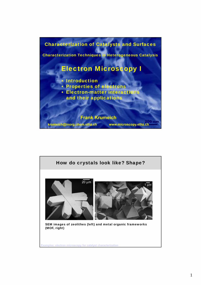
How do crystals look like? Shape?
Examples: electron microscopy for catalyst characterization
SEM images of zeolithes (left) and metal organic frameworks (MOF, right)
2
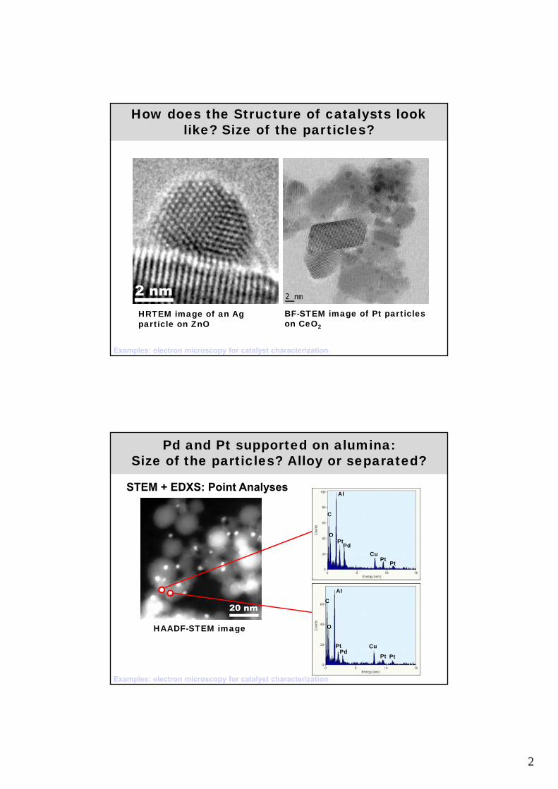
How does the Structure of catalysts look like? Size of the particles?
BF-STEM image of Pt particles on CeO2
HRTEM image of an Ag particle on ZnO
Examples: electron microscopy for catalyst characterization
Pd and Pt supported on alumina: Size of the particles? Alloy or separated?
STEM + EDXS: Point Analyses
HAADF-STEM image
PtPd
PtPt
Cu
Al
O
C
PtPd
Pt Pt
Cu
Al
O
C
Examples: electron microscopy for catalyst characterization
3
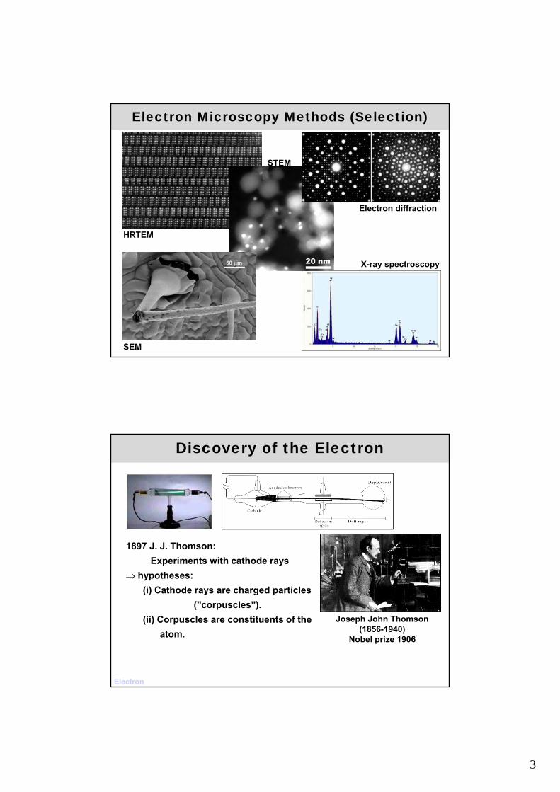
Electron Microscopy Methods (Selection)
HRTEM
SEM
STEM
Electron diffraction
X-ray spectroscopy
Discovery of the Electron
Joseph John Thomson(1856-1940)
Nobel prize 1906
1897 J. J. Thomson:
Experiments with cathode rays
hypotheses:
(i) Cathode rays are charged particles
("corpuscles").
(ii) Corpuscles are constituents of the
atom.
Electron

4
Dualism wave-particle
De Broglie (1924): = h/p = h/mv
: wavelength; h: Planck constant; p: momentum
Accelerated electrons: E = eV = m0v2/2
V: acceleration voltagee / m0 / v: charge / rest mass / velocity of the electron
p = m0v = (2m0eV)1/2
= h / (2m0eV)1/2 ( 1.22 / V1/2 nm)
Relativistic effects:
= h / [2m0eV (1 + eV/2m0c2)]1/2
Electron
Properties of Electrons
Properties of Electrons
Electron
Rest mass of an electron: m0 = 9.109 x 10⁻³¹ kg
Speed of light in vaccuum: c = 2.998 x 10⁸ m/s
Vacc
kV
Nonrel. pm
Rel. pm
Mass x m0Vnonrel x 108 m/s
vrel x
108 m/s
100 3.86 3.70 1.20 1.88 1.64
200 2.73 2.51 1.39 2.65 2.09
300 2.23 1.97 1.59 3.25 2.33
400 1.93 1.64 1.78 3.75 2.48
1000 1.22 0.87 2.96 5.93 2.82
5
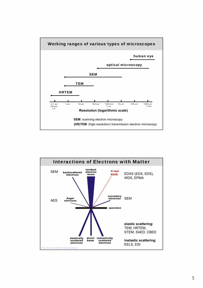
Working ranges of various types of microscopes
0.1 nm100 pm
1 nm 10 nm 100 nm 1000 nm 10 m 100 m 1000 m1 m 1 mm
1 AResolution (logarithmic scale)
human eye
optical microscopy
SEM: scanning electron microscopy
(HR)TEM: (high-resolution) transmission electron microscopy
SEM
TEM
HRTEM
Interactions of Electrons with Matter
EDXS (EDX, EDS), WDS, EPMA
SEM
SEM
AES
elastic scattering:TEM, HRTEM, STEM, SAED, CBED
inelastic scattering:EELS, ESI
Electron-matter interactions
6
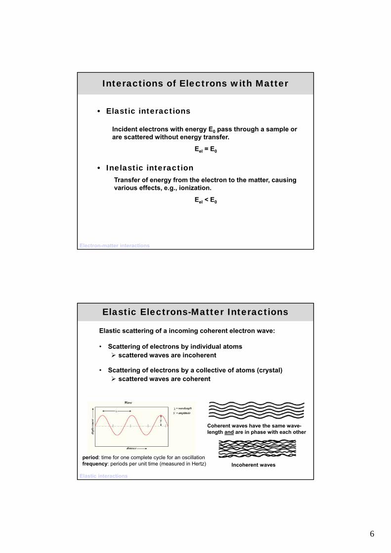
Interactions of Electrons with Matter
• Elastic interactions
• Inelastic interaction
Electron-matter interactions
Incident electrons with energy E0 pass through a sample or are scattered without energy transfer.
Eel = E0
Transfer of energy from the electron to the matter, causing various effects, e.g., ionization.
Eel < E0
Elastic Electrons-Matter Interactions
Elastic scattering of a incoming coherent electron wave:
• Scattering of electrons by individual atoms scattered waves are incoherent
• Scattering of electrons by a collective of atoms (crystal) scattered waves are coherent
Elastic interactions
Coherent waves have the same wave-length and are in phase with each other
Incoherent waves
period: time for one complete cycle for an oscillation frequency: periods per unit time (measured in Hertz)
7
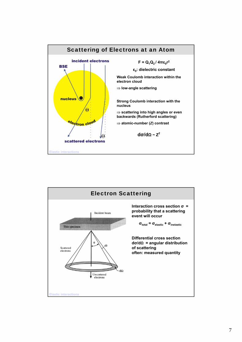
Weak Coulomb interaction within the electron cloud
low-angle scattering
Strong Coulomb interaction with the nucleus
scattering into high angles or even backwards (Rutherford scattering)
atomic-number (Z) contrast
Scattering of Electrons at an Atom
F = Q1Q2 / 4πε0r2
ε0: dielectric constant
Elastic interactions
dσ/dΩ ~ Z2
Electron Scattering
Elastic interactions
Interaction cross section σ = probability that a scattering event will occur
σtotal = σelastic + σinelastic
Differential cross sectiondσ/dΩ = angular distribution of scattering often: measured quantity
8
Elastic Scattering of Electrons
Monte-Carlo simulations of paths of scattered electrons
Elastic interactions
Cu Z=29
AuZ=79 As a general effect of scattering
events, the incoming electron beam is weakened and broadened
brightness of the direct beam
depends on the material contrast between different materials
Amount of high-angle scattering or even backscattering of incident electrons
increases with increasing atomic number (e. g., scattering
cross section Au >> Cu)
decreases with increasing electron energy
Contrast Formation
Elastic interactions
A strong decrease of incoming electron beam intensity occurs
if many atoms scatter, i.e. in thick areas
if heavy atoms scatter

9
Mass-Thickness Contrast
Elastic interactions
Dark contrast in BF-TEM images appears
if many atoms scatter (thick areas darker than thin areas)
if heavy atoms scatter (areas with heavy atoms darker than such with light atoms)
Amorphous SiO2 on C foil
Mainly thickness contrast
Au particles on TiO2
Mainly mass contrast
Bright Field TEM Images
thin
thick
C
Elastic interactions
10
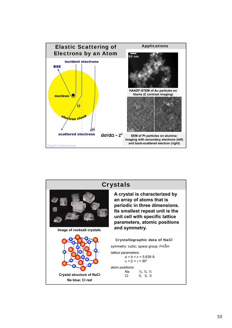
50 nm
HAADF-STEM of Au particles on titania (Z contrast imaging)
SEM of Pt particles on alumina: imaging with secondary electrons (left)
and back-scattered electron (right)
Applications
Elastic interactions
Elastic Scattering of Electrons by an Atom
Elastic interactions
dσ/dΩ ~ Z2
A crystal is characterized by an array of atoms that is periodic in three dimensions. Its smallest repeat unit is the unit cell with specific lattice parameters, atomic positions and symmetry.
Crystals
Image of rocksalt crystals
Crystal structure of NaCl
Na blue; Cl red
Crystallographic data of NaCl
symmetry: cubic; space group: Fm3m
lattice parameters:a = b = c = 5.639 Å = = = 90°
atom positions:Na ½, ½, ½Cl 0, 0, 0
-
11
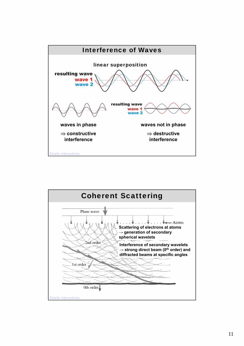
waves in phase
constructive interference
waves not in phase
destructive interference
Elastic interactions
linear superposition
Interference of Waves
Elastic interactions
Coherent Scattering
Scattering of electrons at atoms→ generation of secondary spherical wavelets
Interference of secondary wavelets→ strong direct beam (0th order) and diffracted beams at specific angles
12
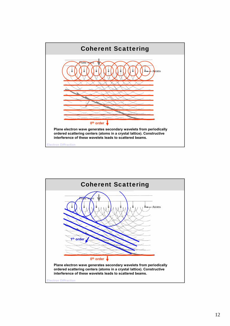
Plane electron wave generates secondary wavelets from periodically ordered scattering centers (atoms in a crystal lattice). Constructive interference of these wavelets leads to scattered beams.
Electron Diffraction
0th order
Coherent Scattering
Plane electron wave generates secondary wavelets from periodically ordered scattering centers (atoms in a crystal lattice). Constructive interference of these wavelets leads to scattered beams.
Electron Diffraction
0th order
1th order
Coherent Scattering

13
Plane electron wave generates secondary wavelets from periodically ordered scattering centers (atoms in a crystal lattice). Constructive interference of these wavelets leads to scattered beams.
Electron Diffraction
0th order
1th order
2th order
Coherent Scattering
Bragg Description of Diffraction
Bragg law: 2dsin = n
Electron Diffraction
Constructive interference between the waves reflected with an angle at atom planes of spacing d occurs if the path difference between the two waves is 2d sin.

14
Electron Diffraction
Bragg law:
2dsin = n
Electron Diffraction
el = 0.00197 nm (1.97 pm) for 300 kV
If d = 0.2 nm = 0.28°
0 > > 1
Reflecting lattice planes are almost parallel to the direct beam
Electron Diffraction on a Lattice
Crystal
Diffraction pattern
Because of small diffraction angles, the electron beam is parallel to the zone axis of the diffracting lattice planes
Electron diffraction pattern of a single crystal
of Al along [111]
Elastic interactions
15
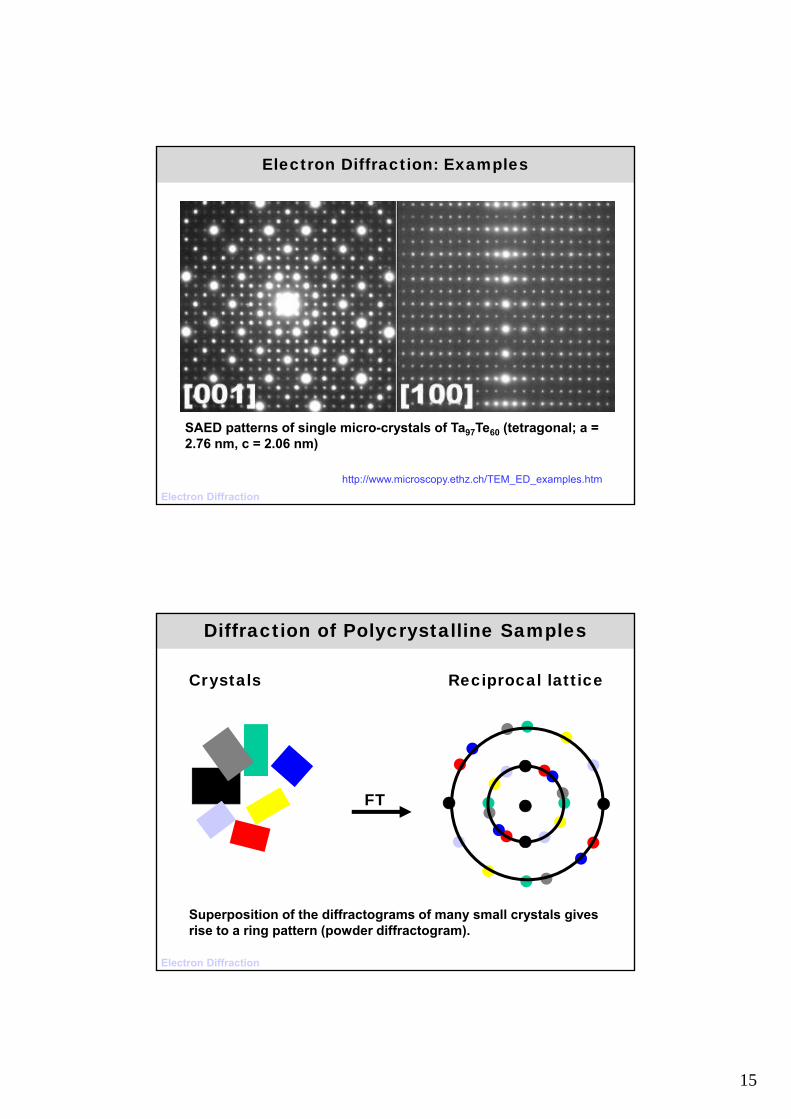
Electron Diffraction: Examples
Electron Diffraction
SAED patterns of single micro-crystals of Ta97Te60 (tetragonal; a = 2.76 nm, c = 2.06 nm)
http://www.microscopy.ethz.ch/TEM_ED_examples.htm
Diffraction of Polycrystalline Samples
Electron Diffraction
Reciprocal latticeCrystals
FT
Superposition of the diffractograms of many small crystals gives rise to a ring pattern (powder diffractogram).
16
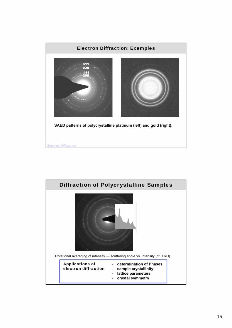
Electron Diffraction: Examples
Electron Diffraction
SAED patterns of polycrystalline platinum (left) and gold (right).
Diffraction of Polycrystalline Samples
Rotational averaging of intensity → scattering angle vs. intensity (cf. XRD)
- determination of Phases- sample crystallinity- lattice parameters - crystal symmetry
Applications of electron diffraction
17
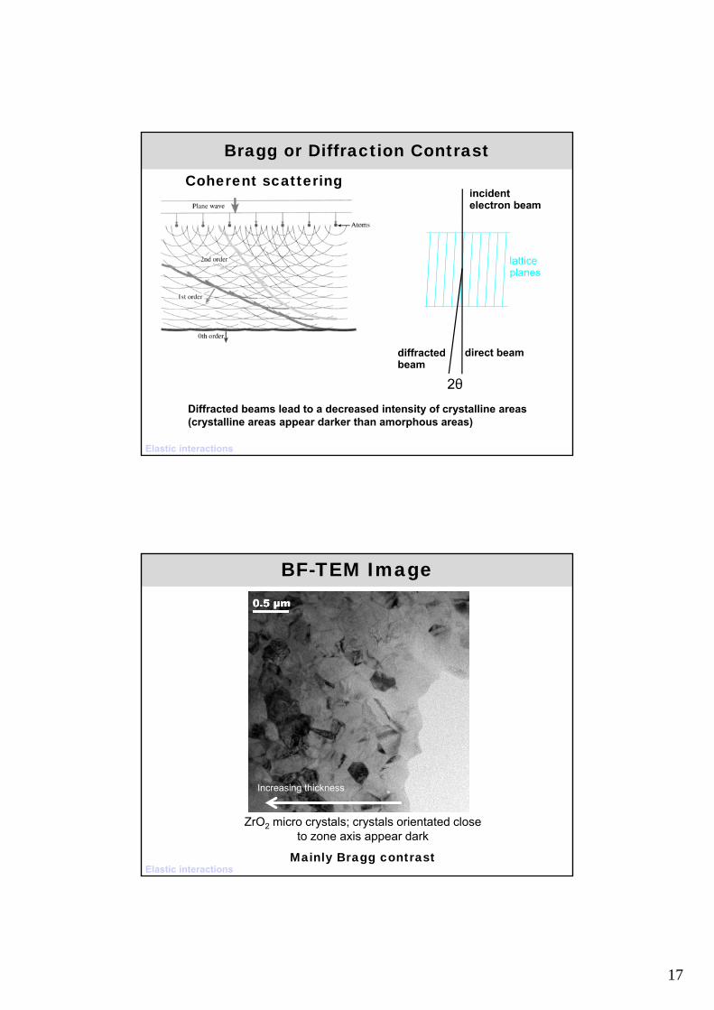
Bragg or Diffraction Contrast
Coherent scattering
Elastic interactions
Diffracted beams lead to a decreased intensity of crystalline areas (crystalline areas appear darker than amorphous areas)
BF-TEM Image
ZrO2 micro crystals; crystals orientated close to zone axis appear dark
Mainly Bragg contrast
Increasing thickness
Elastic interactions
18
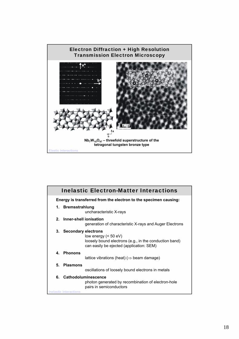
Electron Diffraction + High Resolution Transmission Electron Microscopy
Nb7W10O47 – threefold superstructure of the tetragonal tungsten bronze type
Elastic interactions
Energy is transferred from the electron to the specimen causing:
1. Bremsstrahlunguncharacteristic X-rays
2. Inner-shell ionisationgeneration of characteristic X-rays and Auger Electrons
3. Secondary electronslow energy (< 50 eV) loosely bound electrons (e.g., in the conduction band) can easily be ejected (application: SEM)
4. Phononslattice vibrations (heat) ( beam damage)
5. Plasmonsoscillations of loosely bound electrons in metals
6. Cathodoluminescencephoton generated by recombination of electron-hole pairs in semiconductors
Inelastic Electron-Matter Interactions
Inelastic interactions
19
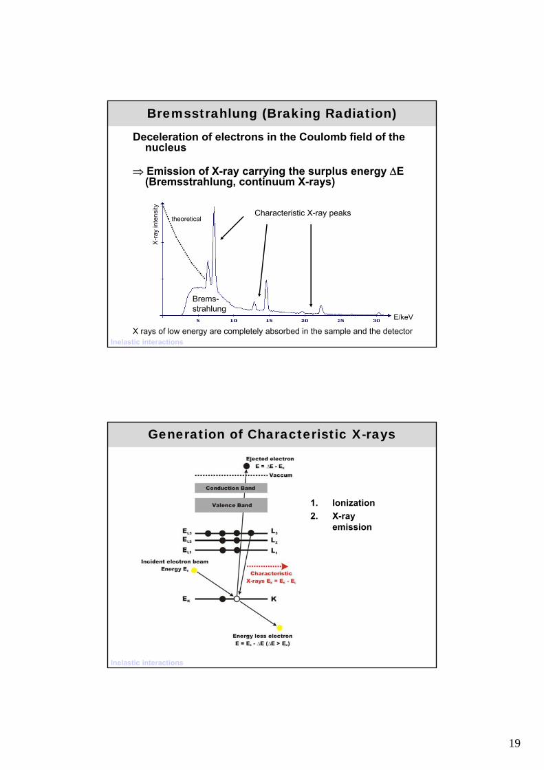
Bremsstrahlung (Braking Radiation)
Characteristic X-ray peaks
E/keV
Brems-strahlung
Deceleration of electrons in the Coulomb field of thenucleus
Emission of X-ray carrying the surplus energy E (Bremsstrahlung, continuum X-rays)
X rays of low energy are completely absorbed in the sample and the detector
theoretical
X-r
ay in
tens
ity
Inelastic interactions
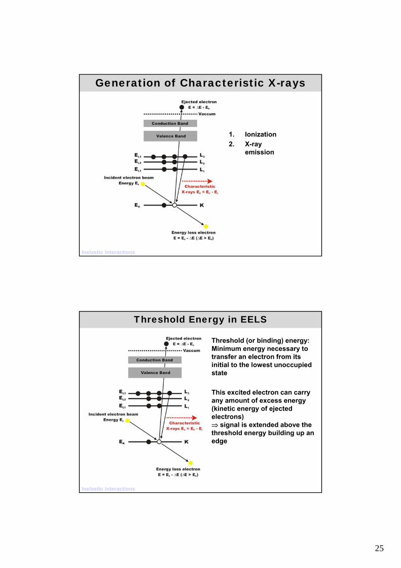
Generation of Characteristic X-rays
1. Ionization
2. X-ray emission
Inelastic interactions

20
1. Ionization
2. X-ray emission
Inelastic interactions
1 2
1
1
Generation of Characteristic X-rays
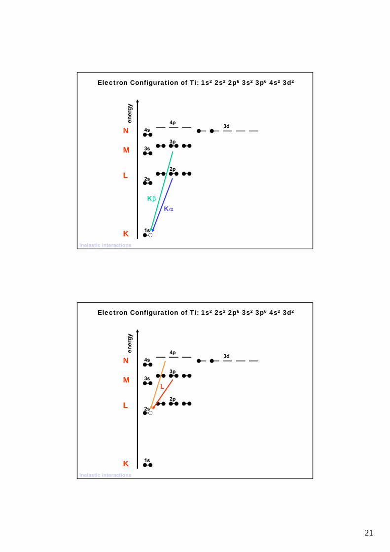
Electron Configuration of Ti: 1s2 2s2 2p6 3s2 3p6 4s2 3d2
ener
gy
1s
2s
3s
4s
2p
3p
4p3d
K
L
M
N
Inelastic interactions
21
Electron Configuration of Ti: 1s2 2s2 2p6 3s2 3p6 4s2 3d2
ener
gy
1s
2s
3s
4s
2p
3p
4p3d
K
L
M
N
K
K
Inelastic interactions
Electron Configuration of Ti: 1s2 2s2 2p6 3s2 3p6 4s2 3d2
ener
gy
1s
2s
3s
4s
2p
3p
4p3d
K
L
M
N
Inelastic interactions
L
22
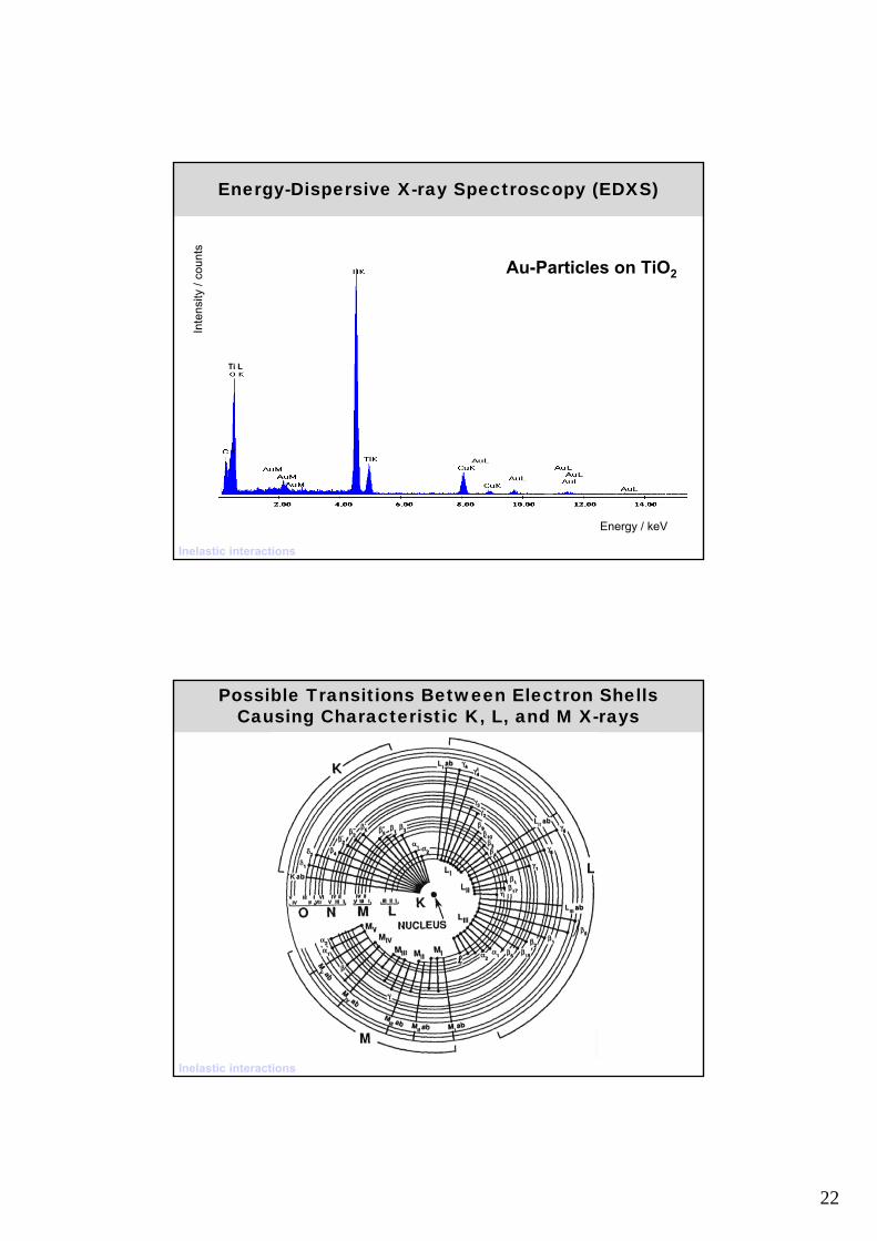
Energy-Dispersive X-ray Spectroscopy (EDXS)
Au-Particles on TiO2
Inte
nsity
/ c
ount
s
Energy / keV
Inelastic interactions
Ti L
Possible Transitions Between Electron Shells Causing Characteristic K, L, and M X-rays
Inelastic interactions
23
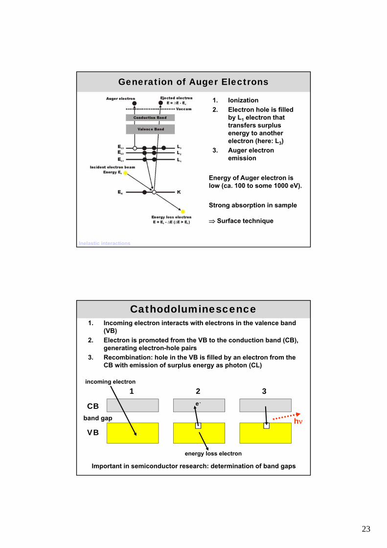
Generation of Auger Electrons
1. Ionization
2. Electron hole is filled by L1 electron that transfers surplus energy to another electron (here: L3)
3. Auger electron emission
Inelastic interactions
Energy of Auger electron is low (ca. 100 to some 1000 eV).
Strong absorption in sample
Surface technique
Cathodoluminescence1. Incoming electron interacts with electrons in the valence band
(VB)
2. Electron is promoted from the VB to the conduction band (CB), generating electron-hole pairs
3. Recombination: hole in the VB is filled by an electron from the CB with emission of surplus energy as photon (CL)
Important in semiconductor research: determination of band gaps
CB
VB
band gap
1 2 3incoming electron
energy loss electron
e-
h

24
Energy is transferred from the electron to the specimen causing:
1. Inner-shell ionization
2. Bremsstrahlung
3. Secondary electrons
4. Phonons
5. Plasmons
6. Cathodoluminescence
Because of energy transfer to the specimen, the electron has adiminished kinetic energy E < E0 after any inelastic scatteringevent.
Inelastic Scattering of Electrons
Inelastic interactions
Electron Energy Loss Spectroscopy
Inelastic interactions
25
1. Ionization
2. X-ray emission
Inelastic interactions
Generation of Characteristic X-rays
Threshold (or binding) energy:Minimum energy necessary to transfer an electron from its initial to the lowest unoccupied state
This excited electron can carry any amount of excess energy (kinetic energy of ejected electrons) signal is extended above the threshold energy building up an edge
Inelastic interactions
Threshold Energy in EELS

26
EELS: Observable Ionization Edges
Inelastic interactions
Edge intensity drops with increasing energy loss
EELS is limited to the appr. energy range 50 - 2000 eV
Almost all elements have observable edges in this energy range:
K edges: Li-SiL edges: Mg-SrM edges: Se-OsN edges: Os-U
Electron Energy Loss Spectroscopy
Inelastic interactions

27
Electron Energy Loss Spectroscopy
Relationship between the EEL Spectrum and a Core-Loss Exication within the Band Structure
ELNES:Electron Energy Loss Near Edge Structure - reflects local density of unoccupied states (DOS)- corresponds to XANES in X-ray absorption spectroscopy
EXELFS:Extended Energy Loss Fine Structure - information on local atomic arrangements - corresponds to EXAFS in X-ray absorption spectroscopy
N(E)
Filled states Empty states
EF E
Extended fine structure
Near edge fine structure
Inelastic interactions
Observation of Fine Structures in EELS
Characteristics of the C_K edge depend on hybridization
Characteristics of the Cu_L2,3
edges depend on oxidation state of Cu
Inelastic interactions
*sp2
sp3

28
Interactions of Electrons with Matter
EXDS (EDX, EDS), WDS, EPMA
SEM
SEM
AES
elastic scattering:TEM, HRTEM, STEM, SAED, CBED
inelastic scattering:EELS, ESI
Electron-matter interactions
Interaction Volume in Compact Samples
Secondary electrons (SE)• Low energy < 50 eV (inelastic interactions)• Information about topology and morphology
Back-scattered electrons (BSE)• High energy E0 (mostly elastic interactions)• Morphology and chemical information
Electron-matter interactions
29
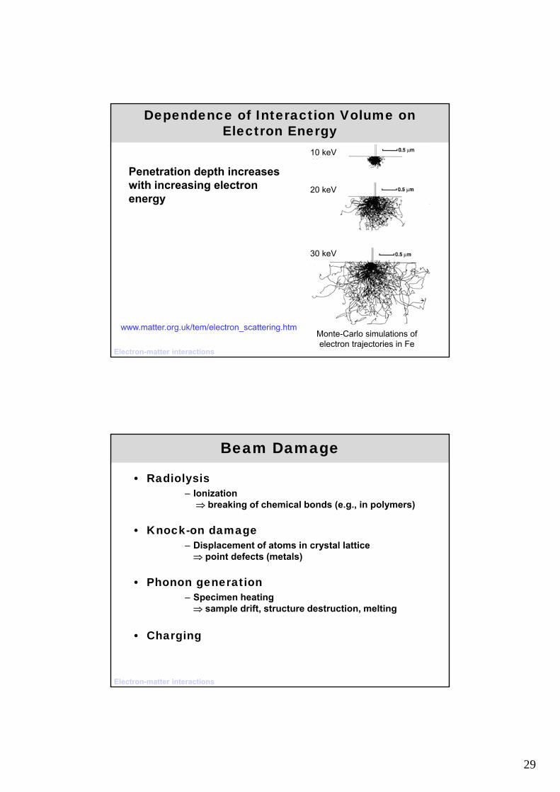
Dependence of Interaction Volume on Electron Energy
Monte-Carlo simulations of electron trajectories in Fe
10 keV
20 keV
30 keV
Penetration depth increases with increasing electron energy
Electron-matter interactions
www.matter.org.uk/tem/electron_scattering.htm
Beam Damage
• Radiolysis– Ionization
breaking of chemical bonds (e.g., in polymers)
• Knock-on damage– Displacement of atoms in crystal lattice point defects (metals)
• Phonon generation– Specimen heating sample drift, structure destruction, melting
• Charging
Electron-matter interactions
30
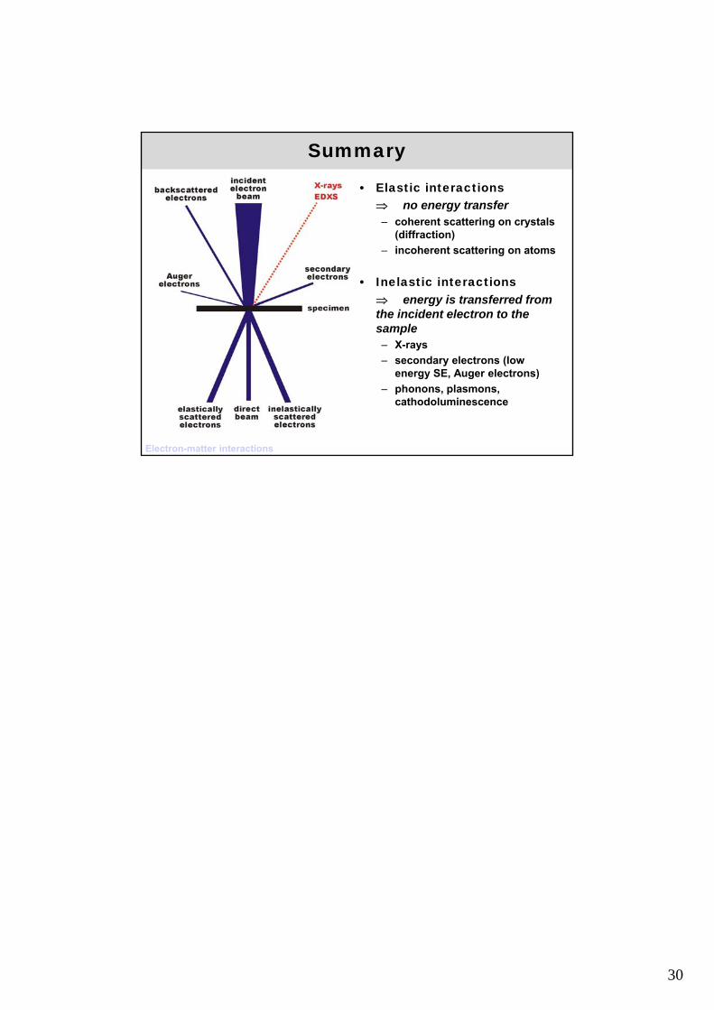
Summary
• Elastic interactions no energy transfer– coherent scattering on crystals
(diffraction)
– incoherent scattering on atoms
• Inelastic interactions energy is transferred from the incident electron to the sample– X-rays
– secondary electrons (low energy SE, Auger electrons)
– phonons, plasmons, cathodoluminescence
Electron-matter interactions