electron probe micro-analysis (epma) 1web.mit.edu/e-probe/www/demo.pdf · sample exchanging chamber...
TRANSCRIPT
Massachusetts Institute of Technology
Electron Probe Micro-Analysis (EPMA)
Electron Microprobe Facility
Department of Earth, Atmospheric and Planetary Sciences
Massachusetts Institute of Technology
Nilanjan Chatterjee, Ph.D.Principal Research Scientist
1
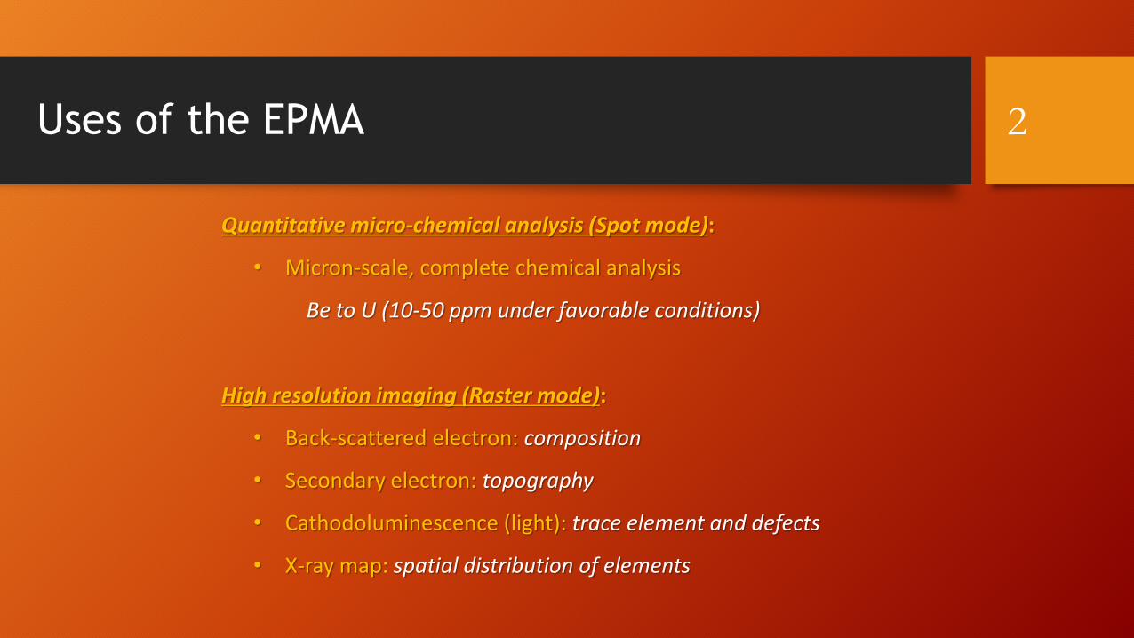
Uses of the EPMA
Quantitative micro-chemical analysis (Spot mode):
• Micron-scale, complete chemical analysis
Be to U (10-50 ppm under favorable conditions)
High resolution imaging (Raster mode):
• Back-scattered electron: composition
• Secondary electron: topography
• Cathodoluminescence (light): trace element and defects
• X-ray map: spatial distribution of elements
2
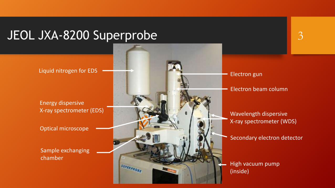
Electron gun
Wavelength dispersiveX-ray spectrometer (WDS)
Energy dispersiveX-ray spectrometer (EDS)
Liquid nitrogen for EDS
Sample exchanging chamber
High vacuum pump(inside)
JEOL JXA-8200 Superprobe
Optical microscope
Electron beam column
Secondary electron detector
3

Signal types
(W hairpin filamentor LaB6 crystal
or field emission-type)
4
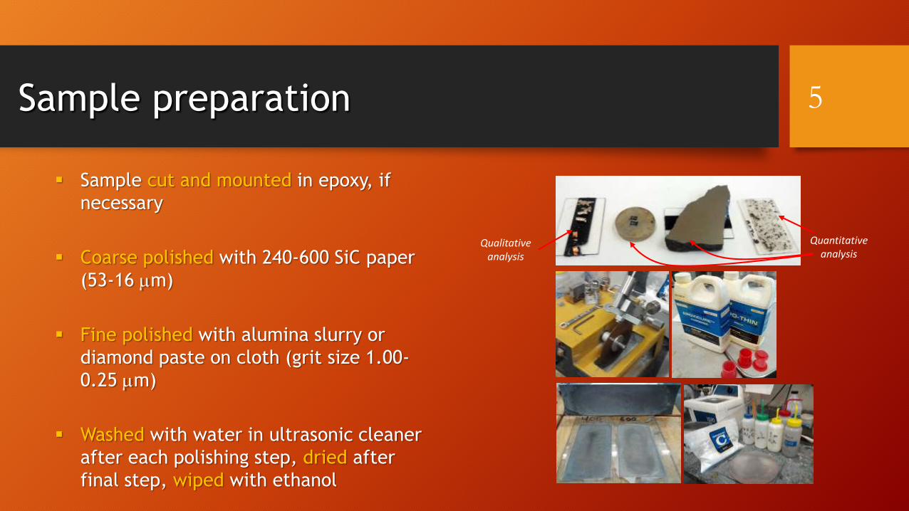
Sample preparation
Sample cut and mounted in epoxy, if
necessary
Coarse polished with 240-600 SiC paper
(53-16 mm)
Fine polished with alumina slurry or
diamond paste on cloth (grit size 1.00-
0.25 mm)
Washed with water in ultrasonic cleaner
after each polishing step, dried after
final step, wiped with ethanol
Qualitativeanalysis
Quantitativeanalysis
5

Carbon coating
Thickness is monitored on a
polished surface of brass,
coated with the samples
25 nm
6
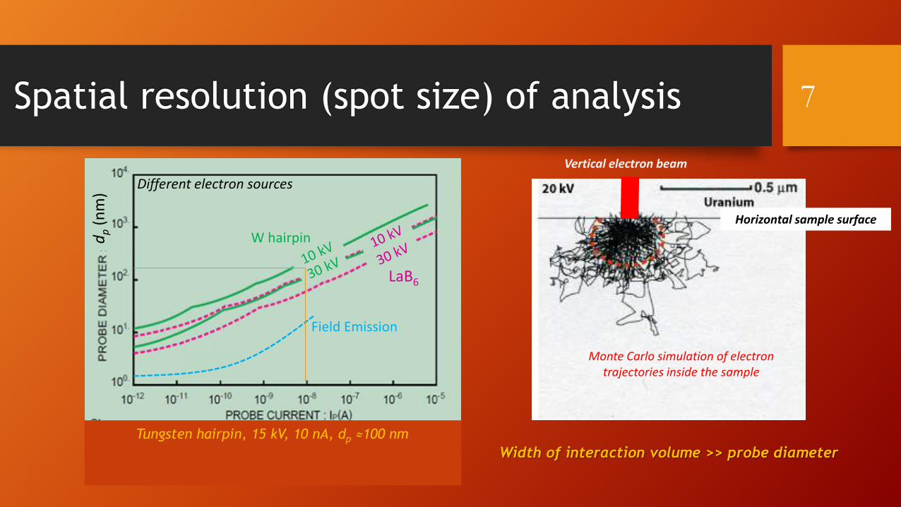
Field Emission
dp
(nm
)
LaB6
W hairpin
Different electron sources
Tungsten hairpin, 15 kV, 10 nA, dp ≈100 nm
Vertical electron beam
Horizontal sample surface
Monte Carlo simulation of electron trajectories inside the sample
Width of interaction volume >> probe diameter
7
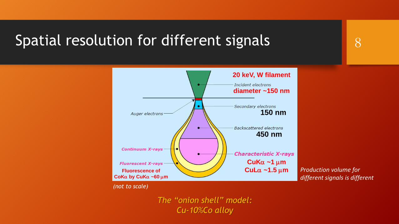
The “onion shell” model:
Cu-10%Co alloy
Production volume for different signals is different
150 nm
450 nm
CuKa ~1 mm
CuLa ~1.5 mmFluorescence of
CoKa by CuKa ~60 mm
20 keV, W filament
diameter ~150 nm
(not to scale)
Spatial resolution for different signals 8

Defocused beam operation
Necessary to use a defocused beam (large spot size) for some types of analysis:
• Fine-grained material groundmass of a porphyritic rock (spot > grain size)
• Na or F containing glass Na migrates away, F migrates toward the spot (~ 10 mm)
• Hydrous glass and minerals amphibole and mica (~ 10 mm)
9
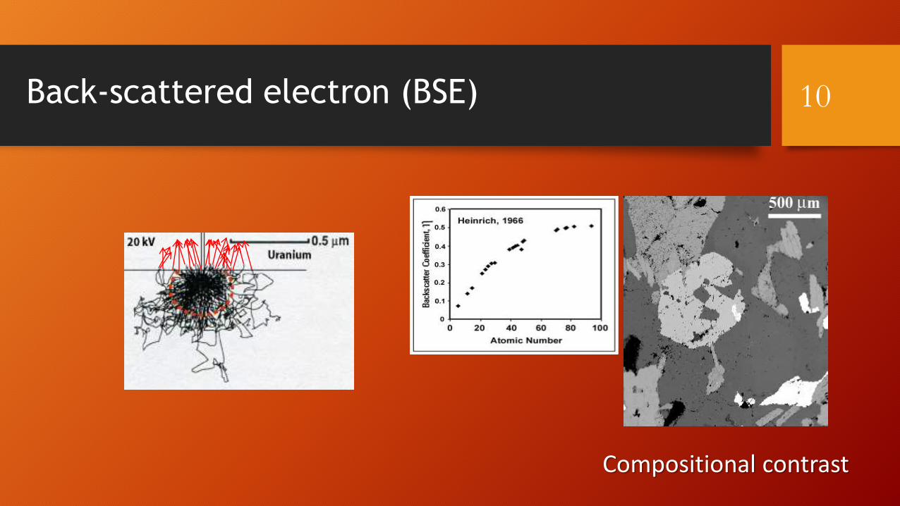
Back-scattered electron (BSE) 10
Compositional contrast
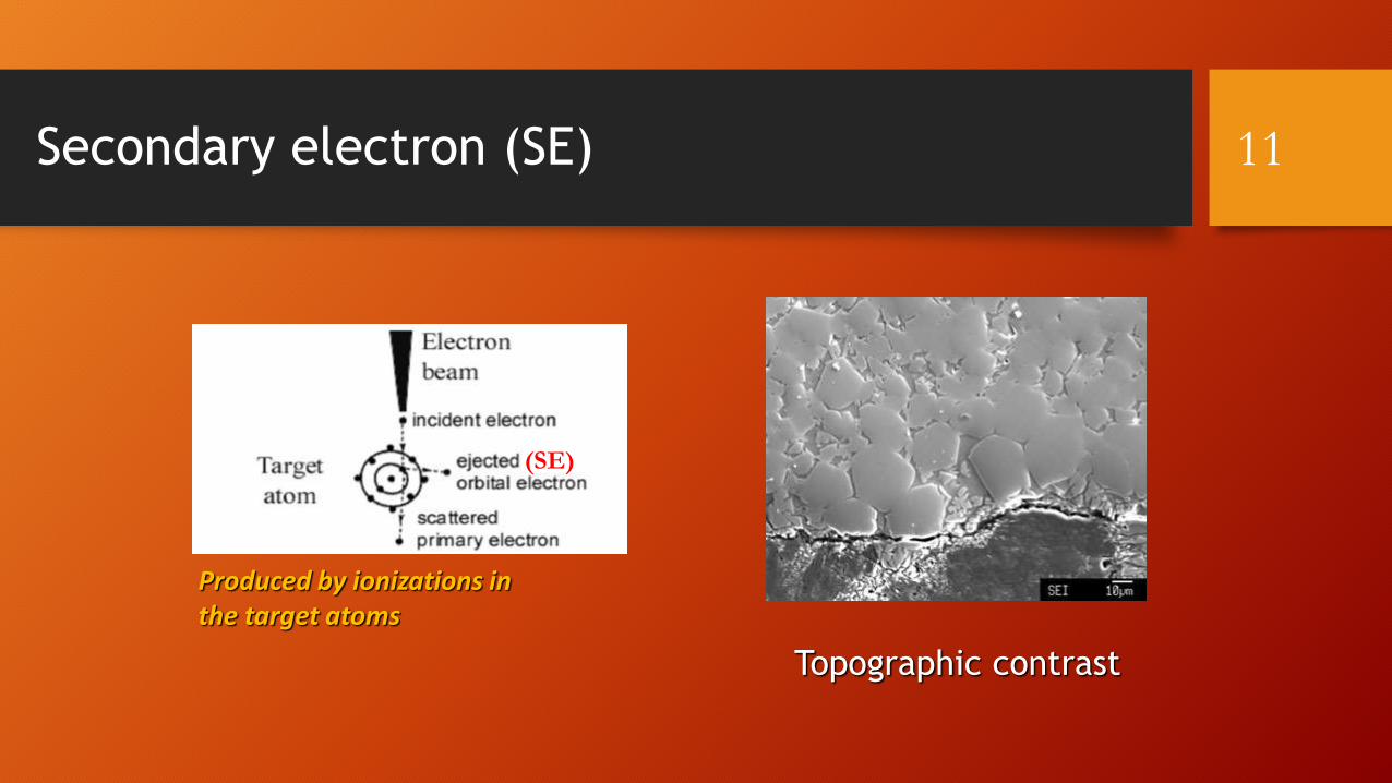
Secondary electron (SE)
Produced by ionizations in the target atoms
(SE)
11
Topographic contrast
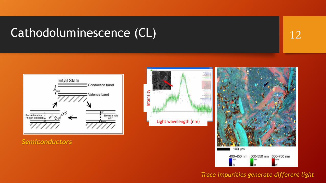
Cathodoluminescence (CL)
Semiconductors
Trace impurities generate different light
12
Light wavelength (nm)
Inte
nsi
ty
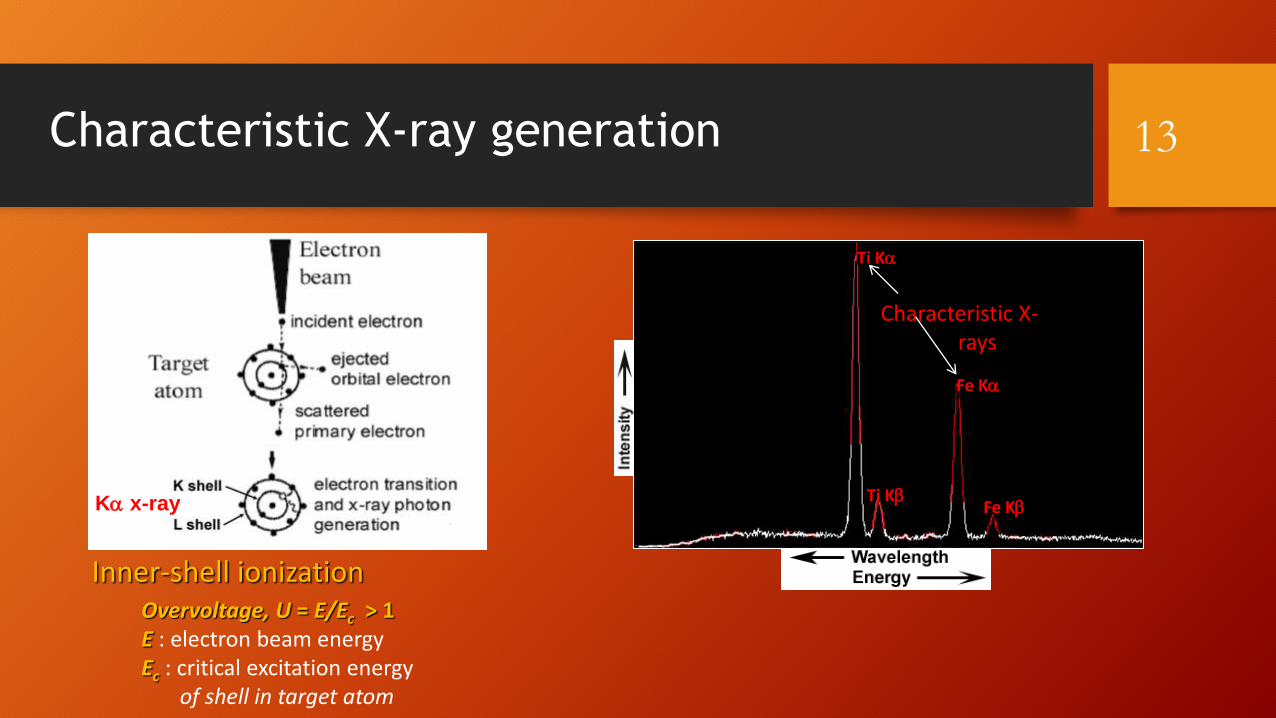
Inner-shell ionization
Ka x-ray
Characteristic X-ray generation
Overvoltage, U = E/Ec > 1E : electron beam energyEc : critical excitation energy
of shell in target atom
13
Characteristic X-rays
Ti Ka
Fe Ka
Ti KbFe Kb
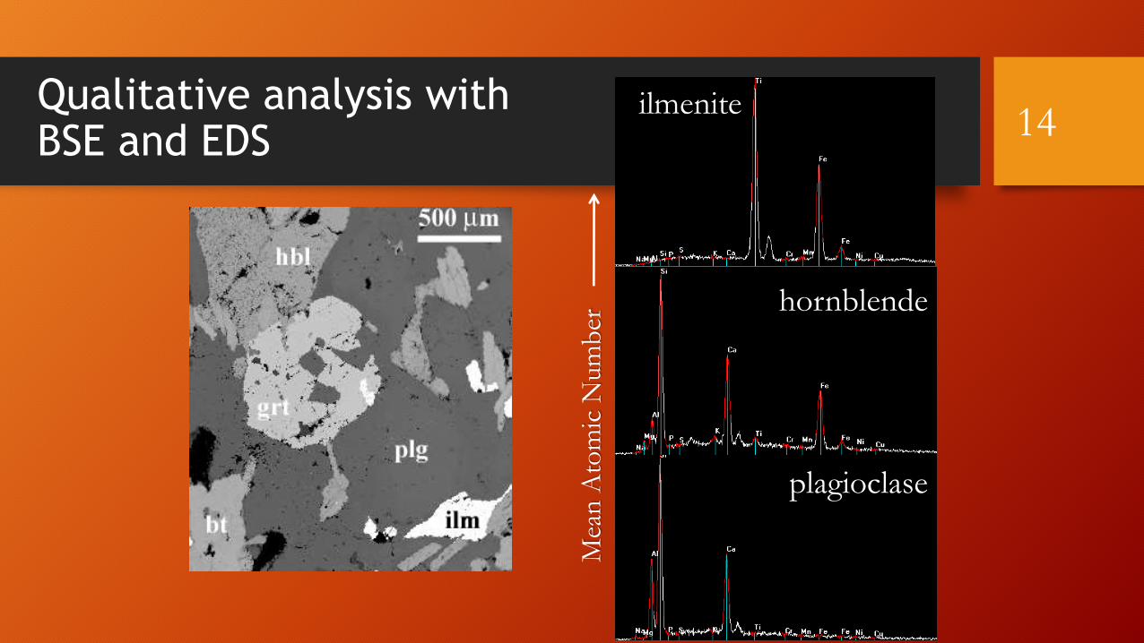
Qualitative analysis withBSE and EDS
ilmenite
plagioclase
hornblende
Mea
n A
tom
ic N
um
ber
14

Wavelength Dispersive Spectrometer (WDS)
Bragg’s Law: nl = 2d sin q
n: order of diffraction
l: wavelength of x-ray
d: lattice spacing in diffracting crystal
q: angle of incidence or diffraction
L: distance between sample and crystal
R: radius of focusing (Rowland) circle
d
l
A
B
Cfor n=1,ABC = 1l
15
sin q =L
2R
“L-value”: L = nlRd

WDS operation
Radius of
focusing circle
(R) is fixed
16

WDS vs. EDS spectral resolution
Peak resolution
with WDS (FWHM ~10 eV)
with EDS (FWHM ~150 eV)
17
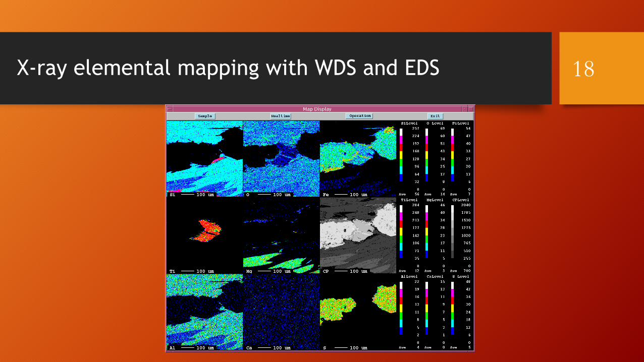
X-ray elemental mapping with WDS and EDS 18

Mapping modes and image quality
• Beam-rastered image:
electron beam rasters over the area to be imaged (defocusing problem)
• Stage-rastered image:
electron beam is stationary, stage moves
19
Image resolution:
number of points measured within the imaged area
X-ray Signal:
beam current and counting (dwell) time per point

Ci , Ii : concentration and intensity in sample
C(i) , I(i) : concentration and intensity in standard
X-ray intensity is proportional to the concentration, 𝐶 ∝ 𝐼
EPMA Quantitative analysis
ZAF Matrix corrections:
Z: Atomic Number correction
A: Absorption correction
F: Fluorescence correction
20

Typical quantitative analysis output
Element k-Ratio El-Wt% MDLel% Ox-Wt% MDLox% At-Prop Error%SiO2 Ka 0.9119 17.30 0.03 37.01 0.05 2.960 0.68%TiO2 Ka 0.0021 0.13 0.05 0.22 0.09 0.013 20.28%Al2O3 Ka 0.5200 11.46 0.03 21.66 0.05 2.042 0.86%Cr2O3 Ka 0.0000 0.00 0.06 0.00 0.08 0.000 99.00%FeO Ka 1.0431 21.43 0.07 27.57 0.09 1.844 1.58%MnO Ka 0.0809 2.89 0.08 3.73 0.11 0.253 4.29%MgO Ka 0.0781 1.36 0.02 2.26 0.04 0.269 2.93%CaO Ka 0.3565 5.20 0.04 7.28 0.05 0.624 1.82%Na2O Ka 0.0011 0.01 0.04 0.02 0.05 0.003 99.00%O 39.95 12.000Total: 99.75 99.75 Cation: 8.007
k-ratio ElementWt%
OxideWt%
Atomicproportion
Minimum detection
limit(El-Wt%)
Minimum detection
limit(Ox-Wt%)
Uncertainty
Cation Sum based on a certain #O
• Typical mineral analysis reports Oxide wt% and Atomic proportions• The wt% total and cation sum give us an idea of the quality of the analysis• Atomic proportions give us the formula: Mg0.27Fe1.84Mn0.25Ca0.62Al2.04Si2.96O12 (garnet)
21
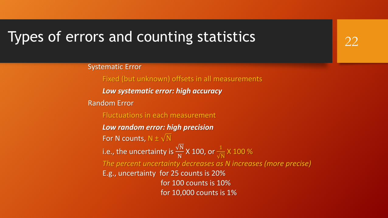
Types of errors and counting statistics
Systematic Error
Fixed (but unknown) offsets in all measurements
Low systematic error: high accuracy
Random Error
Fluctuations in each measurement
Low random error: high precision
22
For N counts, N ± N
i.e., the uncertainty is N
NX 100, or
1
NX 100 %
The percent uncertainty decreases as N increases (more precise)E.g., uncertainty for 25 counts is 20%
for 100 counts is 10%for 10,000 counts is 1%
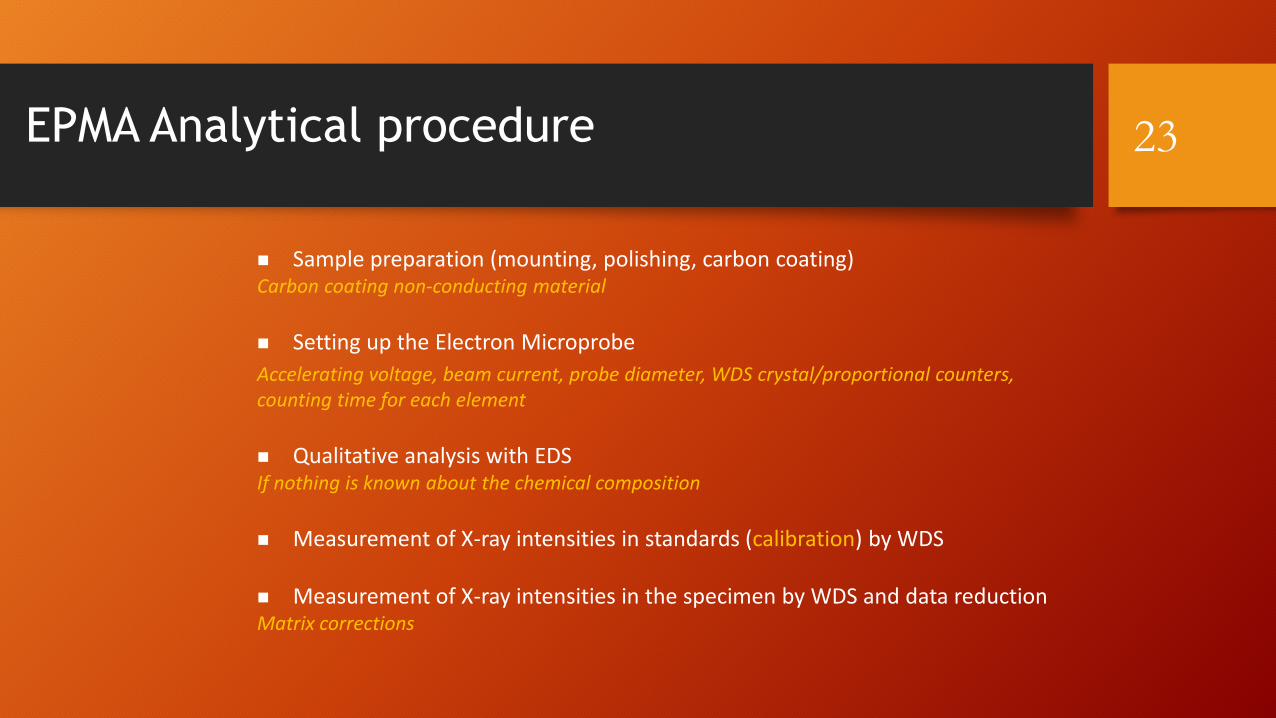
23EPMA Analytical procedure
Sample preparation (mounting, polishing, carbon coating)Carbon coating non-conducting material
Setting up the Electron Microprobe
Accelerating voltage, beam current, probe diameter, WDS crystal/proportional counters, counting time for each element
Qualitative analysis with EDSIf nothing is known about the chemical composition
Measurement of X-ray intensities in standards (calibration) by WDS
Measurement of X-ray intensities in the specimen by WDS and data reductionMatrix corrections