electronic devices and circuit theory · 2019-12-12 ·...
TRANSCRIPT
Link full download: https://www.testbankfire.com/download/solution-manual-for-electronic-devices-and-circuit-theory-11th-edition-by-boylestad-and-nashelsky/
Online Instructor’s Manual for
Electronic Devices and Circuit Theory
Eleventh Edition
Robert L. Boylestad
Louis Nashelsky
Boston Columbus Indianapolis New York San Francisco Upper Saddle River

Amsterdam Cape Town Dubai London Madrid Milan Munich Paris Montreal Toronto Delhi
Mexico City Sao Paulo Sydney Hong Kong Seoul Singapore Taipei Tokyo
Copyright 2013 Pearson Education, Inc., publishing as Prentice Hall, 1 Lake Street, Upper Saddle River,
New Jersey, 07458. All rights reserved. Manufactured in the United States of America. This publication is
protected by Copyright, and permission should be obtained from the publisher prior to any prohibited reproduction,
storage in a retrieval system, or transmission in any form or by any means, electronic, mechanical, photocopying,
recording, or likewise. To obtain permission(s) to use material from this work, please submit a written request to
Pearson Education, Inc., Permissions Department, 1 Lake Street, Upper Saddle River, New Jersey 07458.
Many of the designations by manufacturers and seller to distinguish their products are claimed as trademarks.
Where those designations appear in this book, and the publisher was aware of a trademark claim, the designations
have been printed in initial caps or all caps.
10 9 8 7 6 5 4 3 2 1
ISBN10: 0-13-278373-8
ISBN13: 978-0-13-278373-6
Contents
Solutions to Problems in Text 1
Solutions for Laboratory Manual 209
iii

iv
Chapter 1
1. Copper has 20 orbiting electrons with only one electron in the outermost shell. The fact that
the outermost shell with its 29th electron is incomplete (subshell can contain 2 electrons) and distant from the nucleus reveals that this electron is loosely bound to its parent atom. The application of an external electric field of the correct polarity can easily draw this loosely bound electron from its atomic structure for conduction.
Both intrinsic silicon and germanium have complete outer shells due to the sharing (covalent bonding) of electrons between atoms. Electrons that are part of a complete shell structure require increased levels of applied attractive forces to be removed from their parent atom.
2. Intrinsic material: an intrinsic semiconductor is one that has been refined to be as pure as physically possible. That is, one with the fewest possible number of impurities.
Negative temperature coefficient: materials with negative temperature coefficients have decreasing resistance levels as the temperature increases.
Covalent bonding: covalent bonding is the sharing of electrons between neighboring atoms to form complete outermost shells and a more stable lattice structure.
3. −
4. a. W = QV = (12 µ C)(6 V) = 72 μJ
b. 72 × 10 6 J =
1 eV = 2.625 × 10¹⁴ eV
10
19
1.6 J
5. 48 eV = 48(1.6 10−19 J) = 76.8 10−19 J
W 76.8 10 19
J −18 Q =
=
= 2.40 10 C
V 3.2 V
6.4 10−19 C is the charge associated with 4 electrons.
6. GaP Gallium Phosphide Eg = 2.24 eV
ZnS Zinc Sulfide Eg = 3.67 eV
7. An n-type semiconductor material has an excess of electrons for conduction established by doping an intrinsic material with donor atoms having more valence electrons than needed to establish the covalent bonding. The majority carrier is the electron while the minority carrier is the hole.
A p-type semiconductor material is formed by doping an intrinsic material with acceptor atoms having an insufficient number of electrons in the valence shell to complete the covalent bonding thereby creating a hole in the covalent structure. The majority carrier is the hole while the minority carrier is the electron.
8. A donor atom has five electrons in its outermost valence shell while an acceptor atom has only 3 electrons in the valence shell.
1
9. Majority carriers are those carriers of a material that far exceed the number of any
other carriers in the material. Minority carriers are those carriers of a material that are less in number than any other carrier of the material.
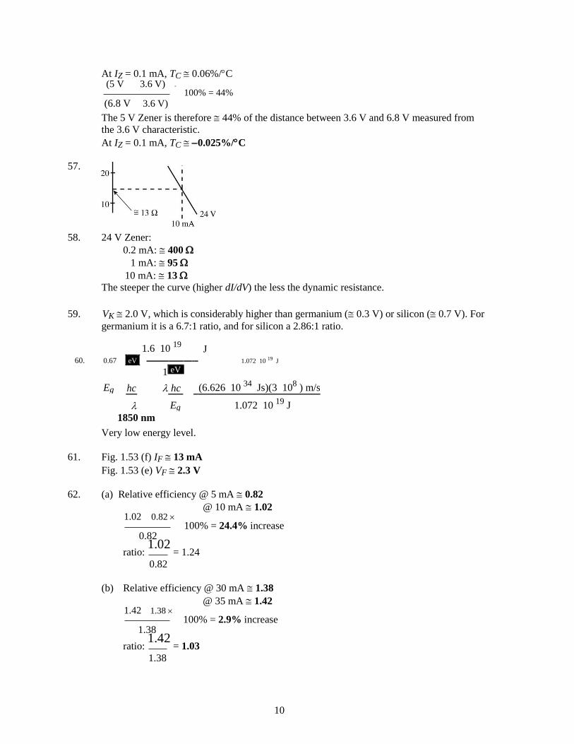
10. Same basic appearance as Fig. 1.7 since arsenic also has 5 valence electrons (pentavalent).
11. Same basic appearance as Fig. 1.9 since boron also has 3 valence electrons (trivalent).
12. −
13. −
14. For forward bias, the positive potential is applied to the p-type material and the negative potential to the n-type material.
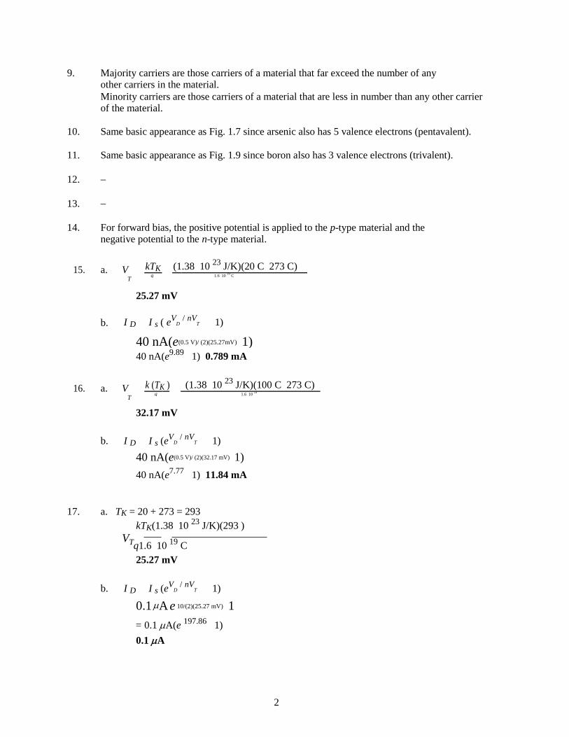
15. a. V kTK (1.38 10 23
J/K)(20 C 273 C) q
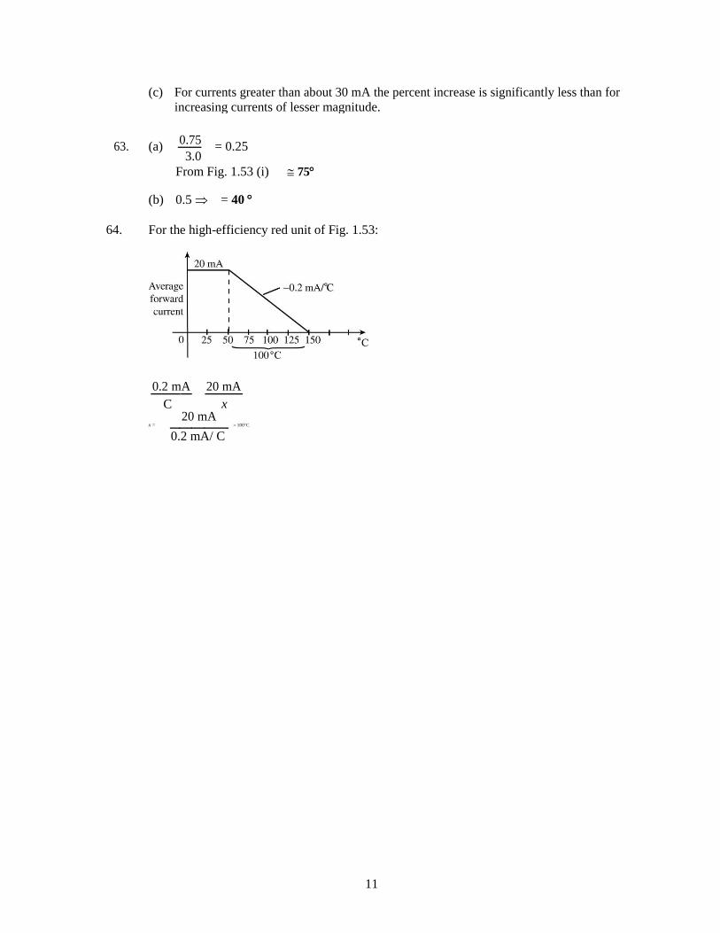
1.6 10 19
C
T
25.27 mV
b. I D I s ( eV
D / nV
T 1)
40 nA(e(0.5 V)/ (2)(25.27mV) 1) 40 nA(e
9.89 1) 0.789 mA
16. a. V k (TK ) (1.38 10 23
J/K)(100 C 273 C) q
1.6 10 19
T
32.17 mV
b. I D I s (eV
D / nV
T 1)
40 nA(e(0.5 V)/ (2)(32.17 mV) 1)
40 nA(e7.77
1) 11.84 mA
17. a. TK = 20 + 273 = 293
kTK(1.38 10 23
J/K)(293 ) VTq1.6 10
19 C
25.27 mV
b. I D I s (eV
D / nV
T 1)
0.1 A e 10/(2)(25.27 mV) 1
= 0.1 A(e 197.86
1)
0.1 A
2
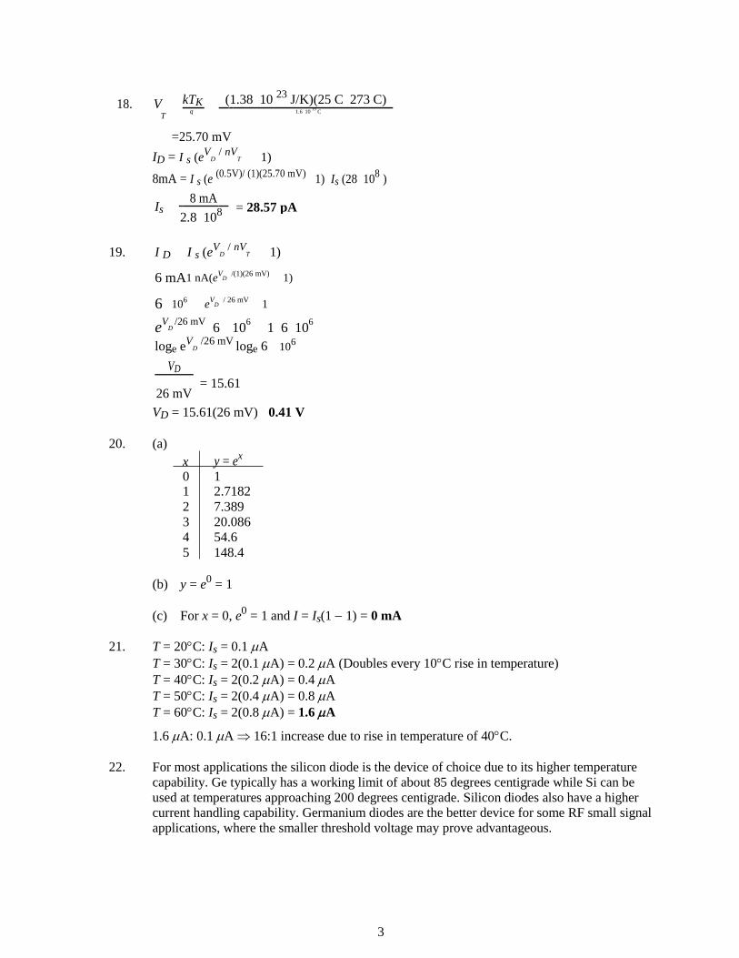
18. V kTK (1.38 10 23
J/K)(25 C 273 C) q
1.6 10 19
C
T
=25.70 mV
ID = I s (eV
D / nV
T 1)
8mA = I s (e (0.5V)/ (1)(25.70 mV)
1) Is (28 108 )
Is
8 mA = 28.57 pA
2.8 108
19. I D I s (eV
D / nV
T 1)
6 mA1 nA(eV
D /(1)(26 mV) 1)
6 106 eV
D / 26 mV 1
eV
D /26 mV
6 106 1 6 10
6
loge eV
D /26 mV
loge 6 106
VD
= 15.61 26 mV
VD = 15.61(26 mV) 0.41 V
20. (a)
x y = ex
0 1 1 2.7182
2 7.389
3 20.086
4 54.6
5 148.4
(b) y = e0 = 1
(c) For x = 0, e0 = 1 and I = Is(1 − 1) = 0 mA
21. T = 20C: Is = 0.1 A
T = 30C: Is = 2(0.1 A) = 0.2 A (Doubles every 10C rise in temperature)
T = 40C: Is = 2(0.2 A) = 0.4 A
T = 50C: Is = 2(0.4 A) = 0.8 A
T = 60C: Is = 2(0.8 A) = 1.6 A
1.6 A: 0.1 A 16:1 increase due to rise in temperature of 40C.
22. For most applications the silicon diode is the device of choice due to its higher temperature
capability. Ge typically has a working limit of about 85 degrees centigrade while Si can be
used at temperatures approaching 200 degrees centigrade. Silicon diodes also have a higher current handling capability. Germanium diodes are the better device for some RF small signal
applications, where the smaller threshold voltage may prove advantageous.
3
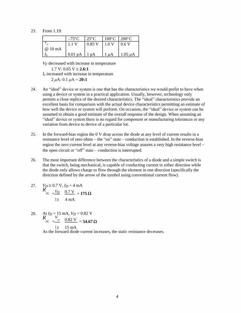
23. From 1.19:
−75C 25C 100C 200C
V
F 1.1 V 0.85 V 1.0 V 0.6 V
@ 10 mA
Is 0.01 pA 1 pA 1 A 1.05 A
VF decreased with increase in temperature
1.7 V: 0.65 V 2.6:1 Is increased with increase in temperature
2 A: 0.1 A = 20:1
24. An “ideal” device or system is one that has the characteristics we would prefer to have when
using a device or system in a practical application. Usually, however, technology only
permits a close replica of the desired characteristics. The “ideal” characteristics provide an
excellent basis for comparison with the actual device characteristics permitting an estimate of
how well the device or system will perform. On occasion, the “ideal” device or system can be
assumed to obtain a good estimate of the overall response of the design. When assuming an
“ideal” device or system there is no regard for component or manufacturing tolerances or any
variation from device to device of a particular lot.
25. In the forward-bias region the 0 V drop across the diode at any level of current results in a
resistance level of zero ohms – the “on” state – conduction is established. In the reverse-bias
region the zero current level at any reverse-bias voltage assures a very high resistance level −
the open circuit or “off” state − conduction is interrupted.
26. The most important difference between the characteristics of a diode and a simple switch is
that the switch, being mechanical, is capable of conducting current in either direction while
the diode only allows charge to flow through the element in one direction (specifically the
direction defined by the arrow of the symbol using conventional current flow).
27. VD 0.7 V, ID = 4 mA
RDC =
VD 0.7 V = 175
I D 4 mA
28. At ID = 15 mA, VD = 0.82 V
RDC =
VD 0.82 V = 54.67
I D 15 mA As the forward diode current increases, the static resistance decreases.
4
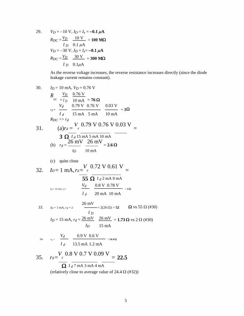
29. VD = −10 V, ID = Is = −0.1 A
RDC = VD 10 V = 100 M
0.1 A I D
VD = −30 V, ID = Is= −0.1 A
RDC = VD 30 V = 300 M
0.1A I D
As the reverse voltage increases, the reverse resistance increases directly (since the diode leakage current remains constant).
30. ID = 10 mA, VD = 0.76 V
RDC =
VD
0.76 V
= 76
I D 10 mA
Vd
0.79 V 0.76 V
0.03 V rd = = 3
I d
5 mA
15 mA 10 mA
RDC >> rd
31. (a)rd = V
d 0.79 V 0.76 V 0.03 V = 3 I d 15 mA 5 mA 10 mA
(b) rd = 26 mV 26 mV
= 2.6
ID 10 mA
(c) quite close
32. ID = 1 mA, rd =V
d 0.72 V 0.61 V = 55 I d 2 mA 0 mA
Vd 0.8 V 0.78 V
ID = 15 mA, rd =
= 2
I d
20 mA 10 mA
26 mV vs 55 (#30) 33. ID = 1 mA, rd = 2
= 2(26 ) = 52
I D
ID = 15 mA, rd = 26 mV 26 mV = 1.73 vs 2 (#30)
ID 15 mA
Vd 0.9 V 0.6 V 34. rav =
= 24.4
I d
13.5 mA 1.2 mA
35. rd =V
d 0.8 V 0.7 V 0.09 V = 22.5 I d 7 mA 3 mA 4 mA
(relatively close to average value of 24.4 (#32))
5
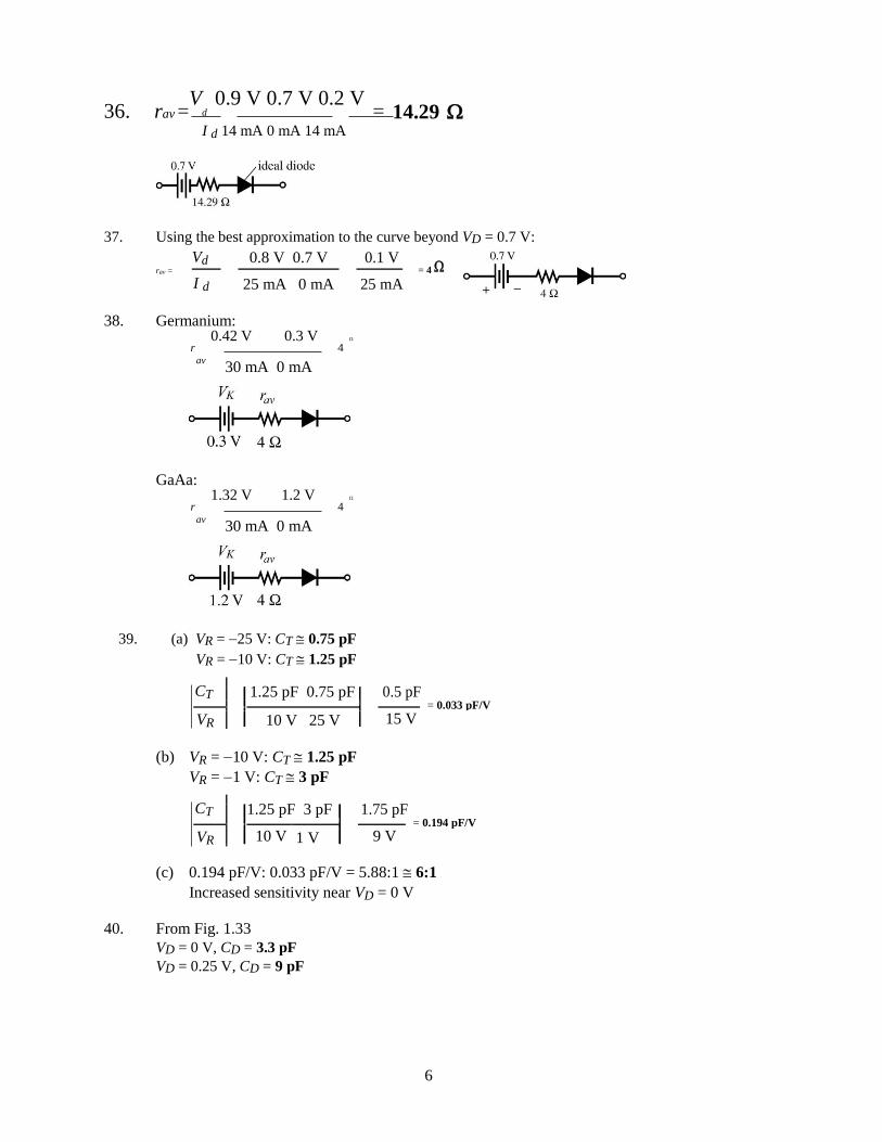
36. rav =V
d 0.9 V 0.7 V 0.2 V = 14.29 I d 14 mA 0 mA 14 mA
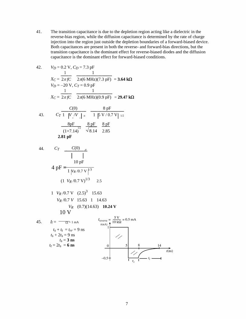
37. Using the best approximation to the curve beyond VD = 0.7 V:
Vd 0.8 V 0.7 V
0.1 V
rav =
= 4
I d 25 mA 0 mA
25 mA
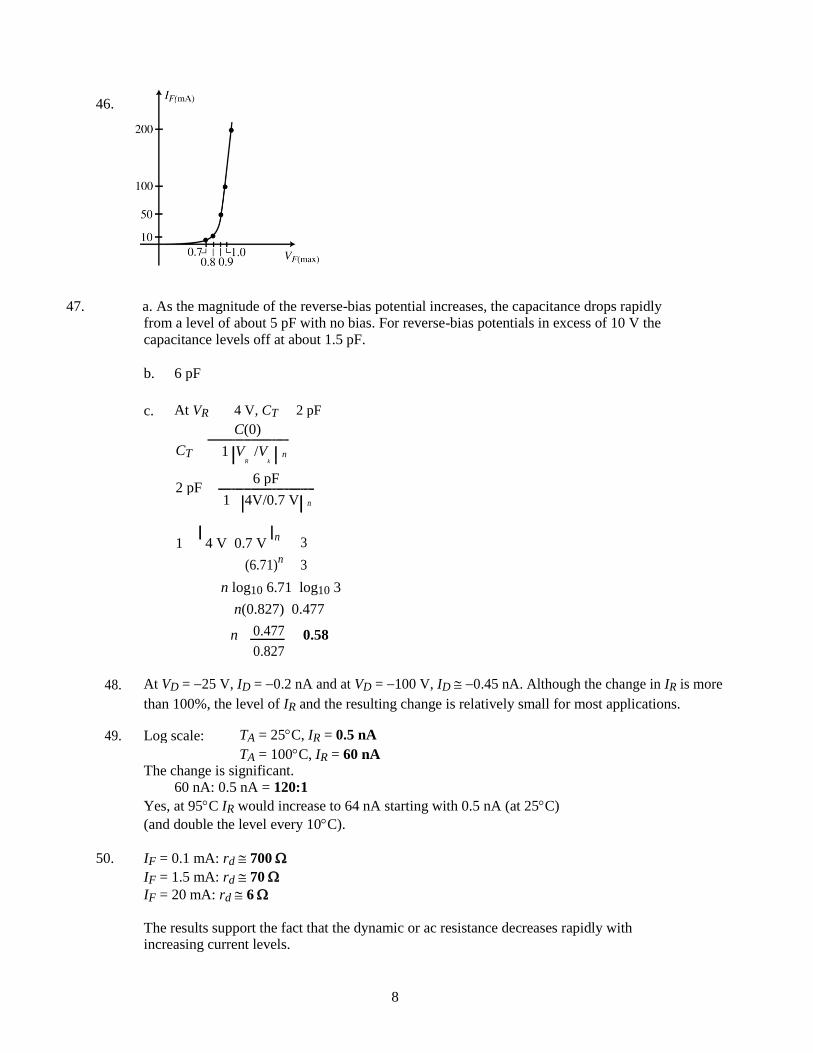
38. Germanium: 0.42 V 0.3 V
r 4 av
30 mA 0 mA
GaAa: 1.32 V 1.2 V
r 4 av
30 mA 0 mA
39. (a) VR = −25 V: CT 0.75 pF
VR = −10 V: CT 1.25 pF
CT
1.25 pF 0.75 pF
0.5 pF
= 0.033 pF/V
VR
10 V 25 V
15 V
(b) VR = −10 V: CT 1.25 pF
VR = −1 V: CT 3 pF
CT
1.25 pF 3 pF
1.75 pF
= 0.194 pF/V
VR
1 V
10 V 9 V
(c) 0.194 pF/V: 0.033 pF/V = 5.88:1 6:1
Increased sensitivity near VD = 0 V
40. From Fig. 1.33
VD = 0 V, CD = 3.3 pF
VD = 0.25 V, CD = 9 pF
6
41. The transition capacitance is due to the depletion region acting like a dielectric in the
reverse-bias region, while the diffusion capacitance is determined by the rate of charge
injection into the region just outside the depletion boundaries of a forward-biased device. Both capacitances are present in both the reverse- and forward-bias directions, but the
transition capacitance is the dominant effect for reverse-biased diodes and the diffusion capacitance is the dominant effect for forward-biased conditions.
42. VD = 0.2 V, CD = 7.3 pF
XC =
1
1
= 3.64 k
2 fC 2(6 MHz)(7.3 pF)
VD = −20 V, CT = 0.9 pF
XC =
1
1
= 29.47 k
2 fC 2(6 MHz)(0.9 pF)
43. CT
C(0)
8 pF
1
V /V
n 1
5 V / 0.7 V
1/2 R K
8pF
8 pF
8 pF
1/2
8.14
(1+7.14) 2.85
2.81 pF
44. CT C(0) 1 VR /V k
10 pF
4 pF = 1 VR /0.7 V
1/3
(1 VR /0.7 V)1/3
2.5
1 VR /0.7 V (2.5)3 15.63
VR /0.7 V 15.63 1 14.63
VR (0.7)(14.63) 10.24 V
10 V
45. If = = 1 mA
ts + tt = trr = 9 ns
ts + 2ts = 9 ns
ts = 3 ns
tt = 2ts = 6 ns
7
46.
47. a. As the magnitude of the reverse-bias potential increases, the capacitance drops rapidly from a level of about 5 pF with no bias. For reverse-bias potentials in excess of 10 V the capacitance levels off at about 1.5 pF.
b. 6 pF
c. At VR 4 V, CT 2 pF
CT
C(0)
1
V /V
n
R k
2 pF
6 pF
1
4V/0.7 V
n
1
4 V 0.7 V
n 3
(6.71)n 3
n log10 6.71 log10 3
n(0.827) 0.477
n 0.477 0.58
0.827
48. At VD = −25 V, ID = −0.2 nA and at VD = −100 V, ID −0.45 nA. Although the change in IR is more
than 100%, the level of IR and the resulting change is relatively small for most applications.
49. Log scale: TA = 25C, IR = 0.5 nA
TA = 100C, IR = 60 nA The change is significant.
60 nA: 0.5 nA = 120:1
Yes, at 95C IR would increase to 64 nA starting with 0.5 nA (at 25C) (and double the level every 10C).
50. IF = 0.1 mA: rd 700
IF = 1.5 mA: rd 70
IF = 20 mA: rd 6
The results support the fact that the dynamic or ac resistance decreases rapidly with increasing current levels.
8
51. T = 25C: Pmax = 500 mW T = 100C: Pmax = 260 mW P
max =
V
FI
F
IF = P
max 500 mW = 714.29 mA VF
0.7 V
IF = P
max 260 mW = 371.43 mA VF
0.7 V 714.29 mA: 371.43 mA = 1.92:1 2:1
52. Using the bottom right graph of Fig. 1.37:
IF = 500 mA @ T = 25C
At IF = 250 mA, T 104C
53.
54. TC = +0.072% = VZ 100%
VZ (T1 T0 )
0.072 = 0.75 V 100
10 V(T1 25)
0.072 = 7.5
T1
25
T1 − 25 = 7.5 = 104.17
0.072
T1 = 104.17 + 25 = 129.17
55. TC = VZ 100%
VZ (T1 T0 )
=
(5 V 4.8 V) 100% = 0.053%/C
5 V(100 25 )
56. (20 V 6.8 V) 100% = 77%
(24 V 6.8 V)
The 20 V Zener is therefore 77% of the distance between 6.8 V and 24 V measured from
the 6.8 V characteristic.
9
At IZ = 0.1 mA, TC 0.06%/C (5 V 3.6 V)
100% = 44% (6.8 V 3.6 V)
The 5 V Zener is therefore 44% of the distance between 3.6 V and 6.8 V measured from
the 3.6 V characteristic.
At IZ = 0.1 mA, TC −0.025%/C
57.
58. 24 V Zener:
0.2 mA: 400
1 mA: 95 10 mA: 13
The steeper the curve (higher dI/dV) the less the dynamic resistance.
59. VK 2.0 V, which is considerably higher than germanium ( 0.3 V) or silicon ( 0.7 V). For
germanium it is a 6.7:1 ratio, and for silicon a 2.86:1 ratio.
1.6 10 19
J 60. 0.67 eV
1.072 10 19 J
1 eV
Eg hc hc (6.626 10 34
Js)(3 108 ) m/s
Eg 1.072 10 19
J
1850 nm
Very low energy level.
61. Fig. 1.53 (f) IF 13 mA
Fig. 1.53 (e) VF 2.3 V
62. (a) Relative efficiency @ 5 mA 0.82 @ 10 mA 1.02
1.02 0.82 100% = 24.4% increase
0.82
ratio: 1.02
= 1.24 0.82
(b) Relative efficiency @ 30 mA 1.38 @ 35 mA 1.42
1.42 1.38 100% = 2.9% increase
1.38
ratio: 1.42
= 1.03 1.38
10
(c) For currents greater than about 30 mA the percent increase is significantly less than for
increasing currents of lesser magnitude.
63. (a) 0.75
= 0.25 3.0
From Fig. 1.53 (i) 75
(b) 0.5 = 40
64. For the high-efficiency red unit of Fig. 1.53:
0.2 mA 20 mA
C x 20 mA x = = 100C
0.2 mA/ C
11
Chapter 2
1. The load line will intersect at ID =
E 12 V
= 16 mA and VD = 12 V. R 750
(a) VDQ 0.85 V
IDQ 15 mA
VR = E − VDQ = 12 V − 0.85 V = 11.15 V
(b) VDQ 0.7 V
IDQ 15 mA
VR = E − VDQ = 12 V − 0.7 V = 11.3 V
(c) VDQ 0 V
ID 16 mA Q
VR = E − VD = 12 V − 0 V = 12 V Q
For (a) and (b), levels of VD and ID are quite close. Levels of part (c) are reasonably close Q Q
but as expected due to level of applied voltage E.
2. (a) ID = E 6 V = 30 mA
0.2 k R
The load line extends from ID = 30 mA to VD = 6 V.
V
D 0.95 V, ID 25.3 mA Q Q
(b) I = E 6 V = 12.77 mA D
R 0.47 k
The load line extends from ID = 12.77 mA to VD = 6 V.
VD 0.8 V, ID 11 mA Q Q
(c) ID =
E 6 V
= 8.82 mA R 0.68 k The load line extends from ID = 8.82 mA to VD = 6 V.
VDQ 0.78 V, IDQ 78 mA
The resulting values of VDQ are quite close, while IDQ extends from 7.8 mA to 25.3 mA.
3. Load line through IDQ = 10 mA of characteristics and VD = 7 V will intersect ID axis as
11.3 mA.
ID = 11.3 mA = E
7 V
R R
7 V with R = = 619.47 k 0.62 kΩ standard resistor
11.3 mA
12
4. (a)ID = IR = E V
D 30 V 0.7 V = 19.53 mA R1.5 k
VD = 0.7 V, VR = E − VD = 30 V − 0.7 V = 29.3 V
(b) ID = E VD
30 V 0 V = 20 mA
R 1.5 k
VD = 0 V, VR = 30 V
Yes, since E VT the levels of ID and VR are quite
close.
5. (a) I = 0 mA; diode reverse-biased.
(b) V20 = 20 V − 0.7 V = 19.3 V (Kirchhoff’s voltage law)
I(20 Ω) = 19.3 V
= 0.965 A
20
V(10 Ω) = 20 V 0.7 V = 19.3 V
I(10 Ω) = 19.3 V
= 1.93 A
10
I = I(10 Ω) + I(20 Ω) = 2.895 A
10 V
(c) I = 10 = 1 A; center branch open
6. (a) Diode forward-biased, Kirchhoff’s voltage law (CW): −5 V + 0.7 V − Vo = 0
Vo = −4.3 V
IR = ID =
Vo
4.3 V = 1.955 mA
R 2.2 k
(b) Diode forward-biased,
ID =
8 V + 6 V 0.7 V = 2.25 mA
1.2 k 4.7 k
Vo = 8 V (2.25 mA)(1.2 kΩ) = 5.3 V
7. (a) Vo = 10 k(12 V 0.7 V 0.3V) = 9.17 V
2 k 10 k (b) Vo = 10 V
13
8. (a) Determine the Thevenin equivalent circuit for the 10 mA source and 2.2 k resistor.
ETh = IR = (10 mA)(2.2 k) = 22 V
RTh = 2. 2k
Diode forward-biased 22 V 0.7 V
ID
= 2.2 k 2.2 k
= 4.84 mA
Vo = ID(1.2 k) = (4.84 mA)(1.2 k)
= 5.81 V (b) Diode forward-biased
ID = 20 V + 20 V 0.7 V = 5.78 mA
6.8 k Kirchhoff’s voltage law (CW):
+Vo − 0.7 V + 20 V = 0 Vo = −19.3 V
9. (a) Vo1 = 12 V – 0.7 V = 11.3 V
Vo2 = 1.2 V
(b) Vo1 = 0 V
Vo2 = 0 V
10. (a) Both diodes forward-biased
Si diode turns on first and locks in 0.7 V drop.
IR 12 V 0.7 V
= 2.4 mA 4.7 k
ID = IR = 2.4 mA
Vo = 12 V − 0.7 V = 11.3 V
(b) Right diode forward-biased: 20 V + 4 V 0.7 V
ID = = 10.59 mA
Vo = 20 V − 0.7 V = 19.3 V
11.(a) Si diode “on” preventing GaAs diode from turning “on”:
I =
1 V 0.7 V
0.3 V = 0.3 mA
1 k 1 k
Vo = 1 V 0.7 V = 0.3 V
(b) I = 16 V 0.7 V 0.7 V + 4 V 18.6 V = 3.96 mA
4.7 k 4.7 k
Vo = 16 V 0.7 V 0.7 V = 14.6 V
14
12. Both diodes forward-biased:
Vo = 0.7 V, Vo = 0.7 V 1 2
I1 k
= 20 V 0.7 V =
19.3 V = 19.3 mA 1 k 1 k
I0.47 k
= 0 mA
I = I1 kΩ I0.47 kΩ = 19.3 mA 0 mA = 19.3 mA
13.
Superposition: V (9.3 V) 1 k(9.3 V) 3.1 V
o 1 k 2 k
1
V (8.8 V) 16 k(8.8 V) 2.93 V
o 1 k 2 k
2
Vo = Vo Vo = 6.03 V 1 2
9.3 V 6.03 V
ID = = 1.635 mA
14. Both diodes “off”. The threshold voltage of 0.7 V is unavailable for either diode.
Vo = 0 V
15. Both diodes “on”, Vo = 10 V − 0.7 V = 9.3 V
16. Both diodes “on”.
Vo = 0.7 V
17. Both diodes “off”, Vo = 10 V
18. The Si diode with −5 V at the cathode is “on” while the other is “off”. The result
is Vo = −5 V + 0.7 V = −4.3 V
19. 0 V at one terminal is “more positive” than −5 V at the other input terminal. Therefore
assume lower diode “on” and upper diode “off”. The result:
Vo = 0 V − 0.7 V = −0.7 V
The result supports the above assumptions.
20. Since all the system terminals are at 10 V the required difference of 0.7 V across either diode cannot be established. Therefore, both diodes are “off” and
Vo = +10 V
as established by 10 V supply connected to 1 k resistor.
15
21. The Si diode requires more terminal voltage than the Ge diode to turn “on”. Therefore,
with 5 V at both input terminals, assume Si diode “off” and Ge diode “on”.
The result: Vo = 5 V − 0.3 V = 4.7 V
The result supports the above assumptions.
22. Vdc = 0.318 Vm Vm =
Vdc
2 V = 6.28 V
0.318 0.318
Im = Vm 6.28 V = 3.14 mA
R2 k
23. Using Vdc 0.318(Vm − VT)
2 V = 0.318(Vm − 0.7 V)
Solving: Vm = 6.98 V 10:1 for Vm:VT
24. Vm = Vdc2 V
= 6.28 V 0.318 0.318
I L = 6.28 V
= 0.628 mA
max
10 k
16
Imax(2 k) = 6.28 V
= 3.14 mA 2 k
I D I L + Imax(2 k) = 0.678 mA + 3.14 mA = 3.77 mA max max
25. Vm = 2 (120 V) = 169.68 V
Vdc = 0.318Vm = 0.318(169.68 V) = 53.96 V
26. Diode will conduct when vo = 0.7 V; that is,
vo = 0.7 V = 1 k(vi )
1 k 1 k
Solving: vi = 1.4 V
For vi 1.4 V Si diode is “on” and vo = 0.7 V.
For vi < 1.4 V Si diode is open and level of vo is determined by voltage divider rule:
vo =
1 k(vi )
= 0.5 vi 1 k 1 k
For vi = −10 V: vo = 0.5(−10 V)
= −5 V
When vo = 0.7 V, v R vi − 0.7 V max max
= 10 V − 0.7 V = 9.3 V
I R
9.3 V = 9.3 mA
max 1 k
Imax(reverse) =
10 V
= 0.5 mA
1 k 1 k
17
27. (a) Pmax = 14 mW = (0.7 V)ID 14 mW
ID = = 20 mA
(b) Imax = 2 × 20 mA = 40 mA
(c) 4.7 k 68 k = 4.4 kΩ
VR = 160 V 0.7 V = 159.3 V 159.3 V
Imax = = 36.2 mA
Id = Imax
= 18.1 mA
2
(d) Total damage, 36.2 mA > 20 mA
28. (a) Vm = 2 (120 V) = 169.7 V
VL = Vi − 2VD m m
= 169.7 V − 2(0.7 V) = 169.7 V − 1.4 V = 168.3 V
Vdc = 0.636(168.3 V) = 107.04 V
(b) PIV =
Vm(load) + VD = 168.3 V + 0.7 V = 169 V
VL 168.3 V (c) ID(max) = m
= 168.3 mA
1 k R
L
(d) Pmax = VDID = (0.7 V)Imax
= (0.7 V)(168.3 mA) = 117.81 mW
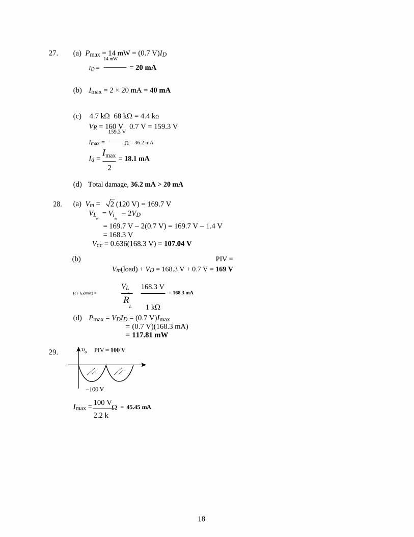
29.
Imax = 100 V
= 45.45 mA
2.2 k
18
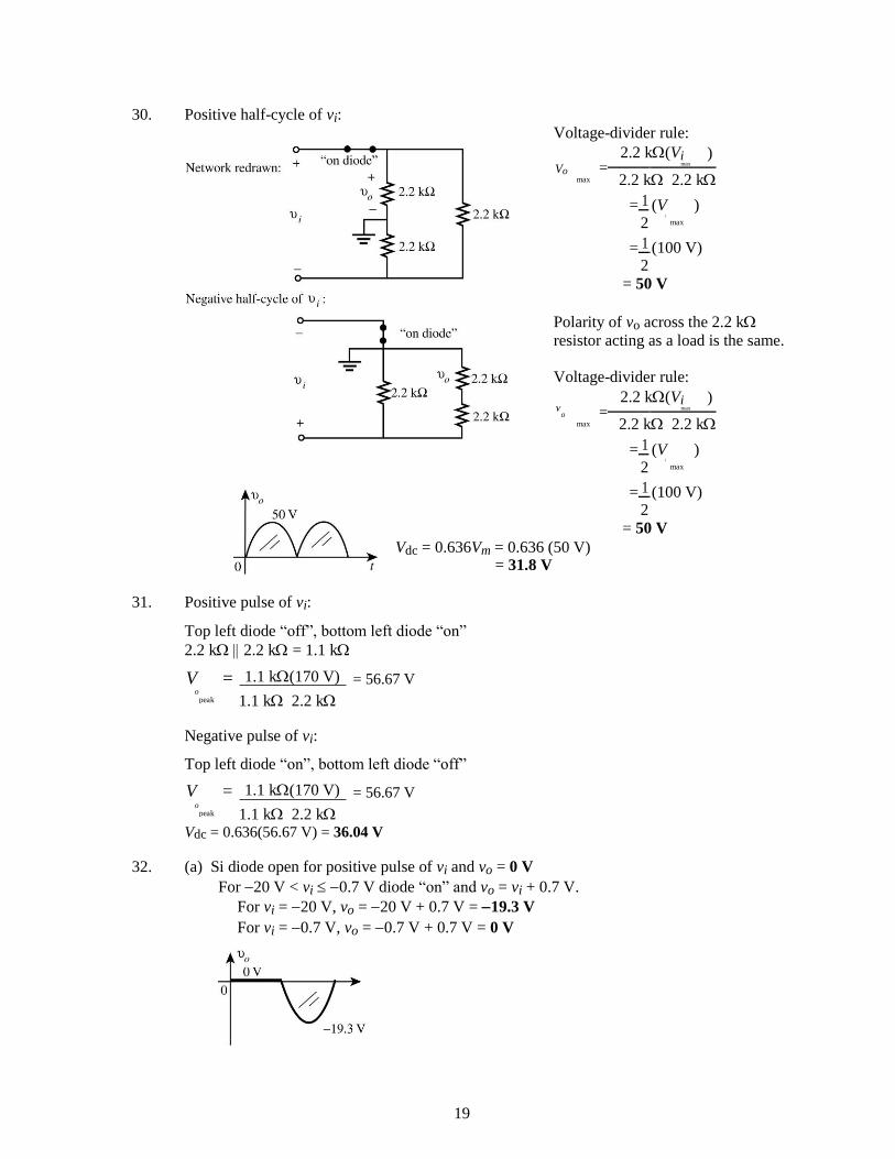
30. Positive half-cycle of vi: Voltage-divider rule:
2.2 k(Vi ) Vo = max
2.2 k 2.2 k max
= 1 (V )
2 i
max
= 1 (100 V)
2 = 50 V
Polarity of vo across the 2.2 k
resistor acting as a load is the same.
Voltage-divider rule:
2.2 k(Vi ) V
o = max
2.2 k 2.2 k max
= 1 (V )
2 i
max
= 1 (100 V)
2 = 50 V
Vdc = 0.636Vm = 0.636 (50 V) = 31.8 V
31. Positive pulse of vi:
Top left diode “off”, bottom left diode “on”
2.2 k 2.2 k = 1.1 k
V = 1.1 k(170 V) = 56.67 V o
1.1 k 2.2 k peak
Negative pulse of vi:
Top left diode “on”, bottom left diode “off”
V = 1.1 k(170 V) = 56.67 V o
1.1 k 2.2 k peak
Vdc = 0.636(56.67 V) = 36.04 V
32. (a) Si diode open for positive pulse of vi and vo = 0 V
For −20 V < vi −0.7 V diode “on” and vo = vi + 0.7 V.
For vi = −20 V, vo = −20 V + 0.7 V = −19.3 V
For vi = −0.7 V, vo = −0.7 V + 0.7 V = 0 V
19
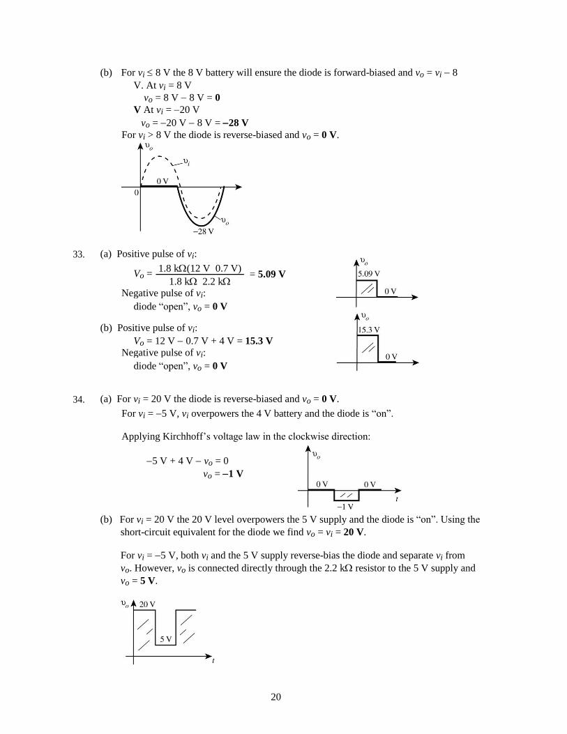
(b) For vi 8 V the 8 V battery will ensure the diode is forward-biased and vo = vi − 8
V. At vi = 8 V vo = 8 V − 8 V = 0
V At vi = −20 V
vo = −20 V − 8 V = −28 V
For vi > 8 V the diode is reverse-biased and vo = 0 V.
33. (a) Positive pulse of vi:
Vo =
1.8 k(12 V 0.7 V) = 5.09 V
1.8 k 2.2 k
Negative pulse of vi:
diode “open”, vo = 0 V
(b) Positive pulse of vi:
Vo = 12 V − 0.7 V + 4 V = 15.3 V
Negative pulse of vi:
diode “open”, vo = 0 V
34. (a) For vi = 20 V the diode is reverse-biased and vo = 0 V.
For vi = −5 V, vi overpowers the 4 V battery and the diode is “on”.
Applying Kirchhoff’s voltage law in the clockwise direction:
−5 V + 4 V − vo = 0
vo = −1 V
(b) For vi = 20 V the 20 V level overpowers the 5 V supply and the diode is “on”. Using the
short-circuit equivalent for the diode we find vo = vi = 20 V.
For vi = −5 V, both vi and the 5 V supply reverse-bias the diode and separate vi from
vo. However, vo is connected directly through the 2.2 k resistor to the 5 V supply and
vo = 5 V.
20
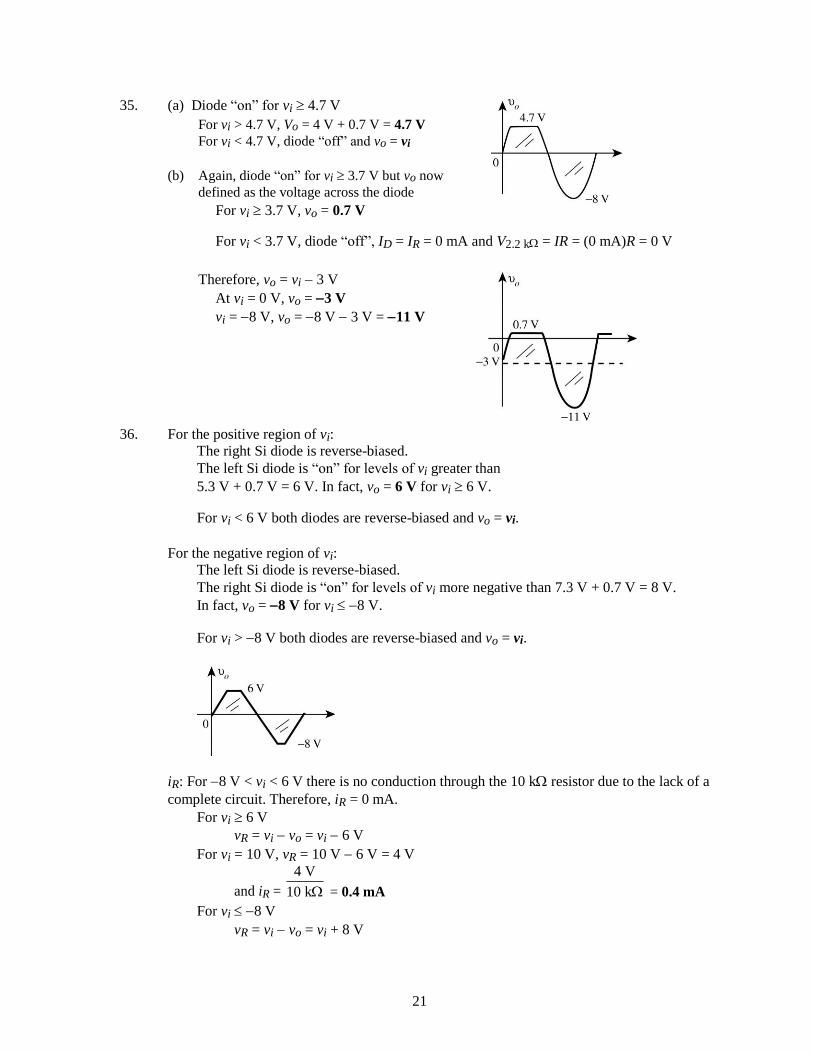
35. (a) Diode “on” for vi 4.7 V For vi > 4.7 V, Vo = 4 V + 0.7 V = 4.7 V
For vi < 4.7 V, diode “off” and vo = vi
(b) Again, diode “on” for vi 3.7 V but vo now
defined as the voltage across the diode For vi 3.7 V, vo = 0.7 V
For vi < 3.7 V, diode “off”, ID = IR = 0 mA and V2.2 k = IR = (0 mA)R = 0 V
Therefore, vo = vi − 3 V At vi = 0 V, vo = −3 V
vi = −8 V, vo = −8 V − 3 V = −11 V
36. For the positive region of vi:
The right Si diode is reverse-biased.
The left Si diode is “on” for levels of vi greater than
5.3 V + 0.7 V = 6 V. In fact, vo = 6 V for vi 6 V.
For vi < 6 V both diodes are reverse-biased and vo = vi.
For the negative region of vi:
The left Si diode is reverse-biased. The right Si diode is “on” for levels of vi more negative than 7.3 V + 0.7 V = 8 V.
In fact, vo = −8 V for vi −8 V.
For vi > −8 V both diodes are reverse-biased and vo = vi.
iR: For −8 V < vi < 6 V there is no conduction through the 10 k resistor due to the lack of a
complete circuit. Therefore, iR = 0 mA.
For vi 6 V
vR = vi − vo = vi − 6 V
For vi = 10 V, vR = 10 V − 6 V = 4 V
and iR =
4 V
= 0.4 mA 10 k For vi −8 V
vR = vi − vo = vi + 8 V
21
For vi = −10 V
vR = −10 V + 8 V = −2 V 2 V
and iR = = −0.2 mA
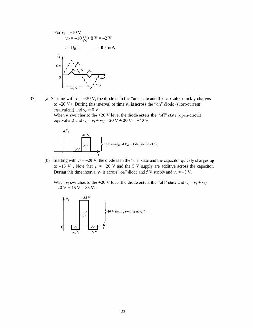
37. (a) Starting with vi = −20 V, the diode is in the “on” state and the capacitor quickly charges
to −20 V+. During this interval of time vo is across the “on” diode (short-current
equivalent) and vo = 0 V. When vi switches to the +20 V level the diode enters the “off” state (open-circuit
equivalent) and vo = vi + vC = 20 V + 20 V = +40 V
(b) Starting with vi = −20 V, the diode is in the “on” state and the capacitor quickly charges up
to −15 V+. Note that vi = +20 V and the 5 V supply are additive across the capacitor.
During this time interval vo is across “on” diode and 5 V supply and vo = −5 V.
When vi switches to the +20 V level the diode enters the “off” state and vo = vi + vC = 20 V + 15 V = 35 V.
22
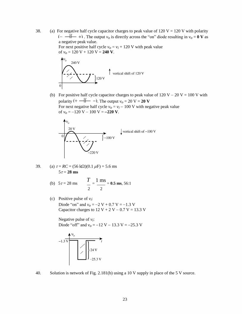
38. (a) For negative half cycle capacitor charges to peak value of 120 V = 120 V with polarity
. The output vo is directly across the “on” diode resulting in vo = 0 V as a negative peak value.
For next positive half cycle vo = vi + 120 V with peak value
of vo = 120 V + 120 V = 240 V.
(b) For positive half cycle capacitor charges to peak value of 120 V − 20 V = 100 V with
polarity . The output vo = 20 V = 20 V
For next negative half cycle vo = vi − 100 V with negative peak value
of vo = −120 V − 100 V = −220 V.
39. (a) = RC = (56 k)(0.1 F) = 5.6 ms
5 = 28 ms
(b) 5 = 28 ms T
= 1 ms
= 0.5 ms, 56:1
2 2
(c) Positive pulse of vi:
Diode “on” and vo = −2 V + 0.7 V = −1.3 V
Capacitor charges to 12 V + 2 V − 0.7 V = 13.3 V
Negative pulse of vi:
Diode “off” and vo = −12 V − 13.3 V = −25.3 V
40. Solution is network of Fig. 2.181(b) using a 10 V supply in place of the 5 V source.
23
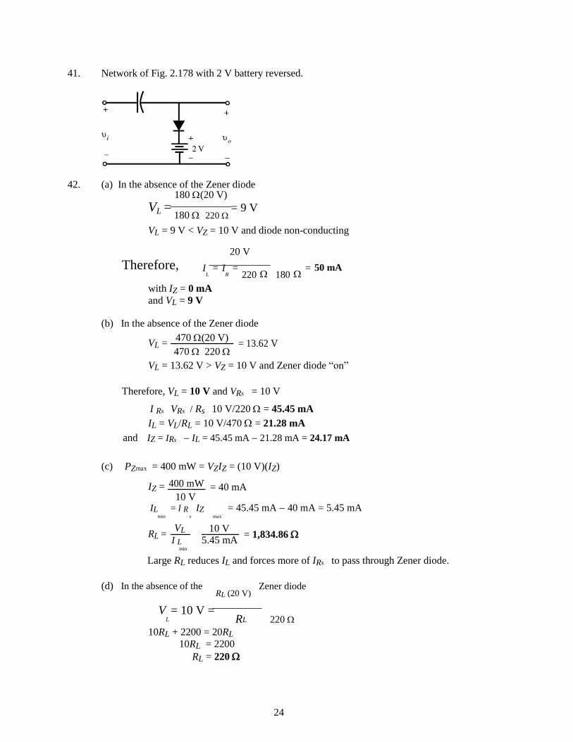
41. Network of Fig. 2.178 with 2 V battery reversed.
42. (a) In the absence of the Zener diode 180 (20 V)
VL =
180 220 = 9 V
VL = 9 V < VZ = 10 V and diode non-conducting
20 V
Therefore,
IL = IR = 220 180 = 50 mA
with IZ = 0 mA
and VL = 9 V
(b) In the absence of the Zener diode
VL = 470 (20 V)
= 13.62 V 470 220
VL = 13.62 V > VZ = 10 V and Zener diode “on”
Therefore, VL = 10 V and VRs = 10 V
I Rs VRs / Rs 10 V/220 = 45.45 mA
IL = VL/RL = 10 V/470 = 21.28 mA
and IZ = IRs − IL = 45.45 mA − 21.28 mA = 24.17 mA
(c) PZmax = 400 mW = VZIZ = (10 V)(IZ)
IZ = 400 mW = 40 mA
10 V
IL = I R IZ = 45.45 mA − 40 mA = 5.45 mA min s max
RL = VL
10 V = 1,834.86 I L
5.45 mA
min
Large RL reduces IL and forces more of IRs to pass through Zener diode.
(d) In the absence of the Zener diode
VL
= 10 V = RL 220
10RL + 2200 = 20RL
10RL = 2200
RL = 220
24
RL (20 V)
43. (a) VZ = 12 V, RL = VL 12 V = 60
I L 200 mA
VL = VZ = 12 V =
RL Vi 60 (16 V)
RL RS 60 Rs
720 + 12Rs = 960 12Rs = 240
Rs = 20
(b) PZmax
= VZ
IZmax
= (12 V)(200 mA) = 2.4 W
44. Since IL = VL VZ is fixed in magnitude the maximum value of IR will occur when IZ is a
RL
RL s
maximum. The maximum level of IR will in turn determine the maximum permissible level s
of Vi.
IZmax
PZ max
400 mW
= 50 mA
VZ
8 V
IL =
VL VZ
8 V = 36.36 mA
R R 220
L L
IRs = IZ + IL = 50 mA + 36.36 mA = 86.36 mA V V
I Rs
i Rs
Z
or
V
i =
I
Rs R
s +
V
Z = (86.36 mA)(91 ) + 8 V = 7.86 V + 8 V = 15.86 V
Any value of vi that exceeds 15.86 V will result in a current IZ that will exceed the maximum value.
45. At 30 V we have to be sure Zener diode is “on”.
VL = 20 V = RLVi
1 k(30 V)
RL Rs
1 k Rs
Solving, Rs = 0.5 k
At 50 V, I R 50 V 20 V
= 60 mA, IL = 20 V
= 20 mA
S 0.5 k 1 k
IZM
= I
R − IL = 60 mA − 20 mA = 40 mA S
46. For vi = +50 V:
Z1 forward-biased at 0.7 V
Z2 reverse-biased at the Zener potential and VZ2 = 10 V.
Therefore, Vo = VZ1 VZ2 = 0.7 V + 10 V = 10.7 V
25
For vi = −50 V:
Z1 reverse-biased at the Zener potential and VZ1 = −10 V.
Z2 forward-biased at −0.7 V.
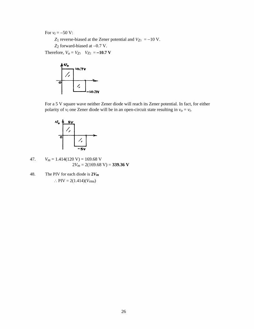
Therefore, Vo = VZ1 VZ2 = −10.7 V
For a 5 V square wave neither Zener diode will reach its Zener potential. In fact, for either
polarity of vi one Zener diode will be in an open-circuit state resulting in vo = vi.
47. Vm = 1.414(120 V) = 169.68 V
2Vm = 2(169.68 V) = 339.36 V
48. The PIV for each diode is 2Vm
PIV = 2(1.414)(Vrms)
26