electronic materials research … materials research laboratory ... thermionic cathode. ... the...
TRANSCRIPT

RESEARCH ON D I G I T A L
TRANSDUCER P R I N C I P L E S
Volume V I 1 1
ELECTRICAL CONDUCTION MECHANISMS I N METAL-
SEMICONDUCTOR-POLYMER T H I N FILM STRUCTURES
ELECTRONIC MATERIALS RESEARCH LABORATORY
THE UNIVERSITY OF TEXAS
COLLEGE OF ENGINEERING
https://ntrs.nasa.gov/search.jsp?R=19700001470 2018-05-15T13:26:53+00:00Z

RESEARCH ON DIGITAL
TRANSDUCER PRINCIPLES
Volme V I I I
ELECTRICAL CONDUCTION MECHANISMS I N METAL-
SEMICONDUCTOR-POLYMER THIN FILM STRUCTURES
f o r t h e
NATIONAL AERONAUTICS AND SPACE ADMINJSTRATION
Grant NGR-44-012-043
Covering t h e Per iod
J u l y 1, 1967 - June 30, 1968
by
Lieh Chun Wang
W i l l i a m H, Hartwig
The Univers i ty of Texas a t Austin
Aust in, Texas 78712

PREFACE
Previous work on Metal-Polymer-Sillcon t h i n f i lm s t r u c t u r e s
by Wilmsen, F i tzg ibbons , Wang, Chuang and Kartwig has been r e p o ~ t e d a s
p a r t of t h e r e sea rch on d i g i t a l t ransducer concepts . The charge t r a n s -
p o r t mechanisms of t h e polymer and behavior of t h e s i l i c o n su r f ace and bulk
were shown t o be r a t h e r complex. The sepa ra t e e f f o r t on polymer f i l m
p r o p e r t i e s , a s r epo r t ed i n Volume VIII, shows behaviors which can be
a t t r i b u t e d t o t h e d i e l e c t r i c a lone , It i s necessary t o form t h e e n t i r e
MPS s t r u c t u r e t o observe c h a r a c t e r i s t i c s of t h e s i l i c o n su r f ace , As a
r e s u l t , a s e p a r a t e p r o j e c t was undertaken t o measure more c a r e f u l l y t h e
combined behavior and then reso lve t h e s i l i c o n su r f ace (and bu lk ) e f f e c t s .
P a r a l l e l work from t h e l i t e r a t u r e on MOS F i e l d Ef fec t T r a n s i s t o r s
was found t o provide some c lues as t o t h e expected behavior , but it must be
r e a l i z e d t h e s e devices have very t h i c k i n s u l a t i n g l a y e r s compared t o
t hose under s tudy he re , Since t h e charge t r a n s p o r t i s an exponent ia l func-
t i o n of t h i ckness (whatever t h e mechanisms), d i e l e c t r i c s which a r e only 0
100 A t h i c k would be expected t o have a more c r i t i c a l r o l e , This i s
d e l i b e r a t e , s i n c e eventua l t ransducer behavior would draw, i n some ways,
upon t h e p r o p e r t i e s of t h e d i e l e c t r i c f i l m s . By making f a m i l i a r capaci tance
vs vol tage p l o t s i n add i t i on t o log cur ren t dens i ty vs square roo t of
vo l tage p l o t s , t h e e f f e c t s of s i l i c o n su r f ace s t a t e s were t o be reso lved .
From a knowledge of t h e vol tage-current d e n s i t y behavior of t h e polymer
a lone , t h e f i e l d pene t r a t ion i n t o t h e s i l i c o n could be measured from
reverse-biased d a t a , From t h e d i f fe rences , s u i t a b l y cor rec ted f o r work-
func t ion e f f e c t s , would come t h e sepa ra t e vo l t age drops across t h e polymer
and s i l i c o n dep le t ion l a y e r , I f succes s fu l , t h e increased knowledge would
be use fu l i n c o n t r o l of t he break characteristics of t h e reverse-biased MPS
s t r u c t u r e ,


ABSTRACT
Elec t ron conduction mechanisms of metal-polymer-semiconductor
systems were i n v e s t i g a t e d i n t h i s p r o j e c t . Samples were made on N-type
s i l i c o e of r e s i s t i v i t y range 10R-cm t o 150R-cm. A low energy e l e c t r o n
(2350 ev ) gun was employed topolymerize t h e D . C . 704 pump o i l used i n
the vacuum system. Metals of A 1 and Ag were evaporated on t h e polymer
as t o p e l e c t r o d e .
Poole-Frenkel e f f e c t s have been observed a s t h e dominating
conduction mechanism of t h e polymer. However, t h e I - V c h a r a c t e r i s t i c s
of MPS devices a r e d i f f e r e n t i n t h e forward and reverse b i a s condi t ions .
In forward d i r e c t i o n , t h e cu r r en t i s dominated by t h e f i e l d w i th in t h e
polymer and inc reases exponent ia l ly wi th b i a s vol tage i n t h e f a sh ion
of Poole-Frenkel e f f e c t . I n t he r eve r se d i r e c t i o n , t h r e e d i s t i ngu i sh -
ab le reg ions may be obta ined f o r t h e I - V c h a r a c t e r i s t i c s on a I n J vs
V p l o t . These were i n t e r p r e t e d i n terms of t h e propor t ion of vo l t age
drops across t h e polymer and semiconductor t o t h e t o t a l b i a s vo l t ages .
The genera t ion of e lectron-hole p a i r s i n t h e deple t ion l a y e r of t h e
semiconductor l i m i t s t h e cur ren t flow i n t h e reverse b i a s condi t ion
and cur ren t s a t u r a t i o n may be observed.
The I - V c h a r a c t e r i s t i c s of MPS devices were found extremely
s e n s i t i v e t o s i l i c o n su r f ace p repa ra t ion . Strong chemical e t ch ing was
p r e f e r r e d f o r observing cu r ren t s a t u r a t i o n s .
The experimental values of t h e s lope of i n a us . E ~ ' ~ / B T f e l l
i n t h e range of 6 . 5 5 x t o 8 .7 x and t h e zero f i e l d conductiv-
-16 i t y was 10 and 10-17 mhos /em.
TABLE OF CONTENTS
Page
. . . . . . . . . . . . . . . . . . . . . . . . . . . . . . PREFACE i~
. . . . . . . . . . . . . . . . . . . . . . . . . . . . . ABSTRACT V
A . Chemica lS t ruc tu re . . . . . . . . . . . . . . . . . . . . . 1
B . Poss ib l e Conduction Mechanisms . . . . . . . . . . . . . . . 3
1 . I o n i c Conduction . . . . . . . . . . . . . . . . . . . . 4
2 . Space-charge-limited Flow . . . . . . . . . . . . . . . 4
3 . Tunneling o r F i e l d Emission . . . . . . . . . . . . . . 5
4 . Schot tkyEmiss ion . . . . . . . . . . . . . . . . . . . . 5
5 . The Poole-Frenkel E f f e c t . . . . . . . . . . . . . . . . 5
C . Limi ta t ion of The Theore t i ca l Approach . . . . . . . . . . . 5
. . . . . . . . . . . . . . . . . . . . . . . . . . . . . 11 . THEORY 9
A . Conduction Processes through Thin I n s u l a t i n g Films . . . . . 9
1 . Schot tkyEmiss ion . . . . . . . . . . . . . . . . . . . . 9
2 . Tunneling . . . . . . . . . . . . . . . . . . . . . . . 12
. . . . . . . . . . . . . . . . . . 3 . Poole-Frenkel E f f e c t 15
B. Semiconductor Surface S t a t e s and D-C Current Sa tu ra t ion . . . 20
. . . . . . . . . . . . . . . . . . . . I11 . EXPERIMENTAL PROCEDURES 27
. . . . . . . . . . . . . . . . . . . . . . A Sample P repa ra t ion 27
. . . . . . . . . . . . . . . . . . . . . . I3 . Back Side Contact 28
. . . . . . . . . . . . . . . . . . . . . . C Polymer Formation 30
. . . . . . . . . . . . . . . . . . . . D E l e c t r o p l a t e Deposition 31

I V . EXPERIMENTAL RESULTS . .
vi i
Page
. . 34
A . Conduction P rope r t i e s of Pol-;per . . . . . . . . . . . . . 35
. . . . . . . . . . . . . . . . . . . B . Data of MPS Devices 38
C . An explanat ion of I-V C h a r a c t e r i s t i c s of MPS Devices i n R e v e r s e B i a s Condition . . . . . . . . . . . . . . . . 44
. . . . . . . . . . . . . . . . . . . . . . . . V . CONCLUSION.. 59
VITA . . . . . . . . . . . . . . . . . . . . . . . . . . . . . . . 64

Numb e r
LIST OF FIGURES
Page
Energy-band Diagram of MIS I n t e r f a c e i n Equilibrium 9
One-dimensional Tunneling 12
An I n s u l a t o r Band Model. E and E a r e energy l e v e l s f o r Traps and Donors
t d 16
Mechanism of Poole-Frenkel E f f e c t 18
P o t e n t i a l Energy of an E lec t ron wi th in Per iodic C r y s t a l L a t t i c e
Cathode Ray Tube C i r c u i t 31
Tes t ing Sample Connection 3 2
Current versus square r o o t vo l t age of MPS device 37
I - V C h a r a c t e r i s t i c s of MPS Devices (Group 1)
I-V C h a r a c t e r i s t i c s of MPS Devices (Group 2 ) 40
I -V C h a r a c t e r i s t i c s of MPS Devices (Group 3 ) 4 1
I-V C h a r a c t e r i s t i c s of MPS Devices ( ~ r o u ~ 4 ) 42
Conductivity Versus Square-root of E l e c t r i c F i e l d 45
( a ) I - V C h a r a c t e r i s t i c s of Sample #81 47
( b ) Current versus vol tage drop across t h e semiconductor o f Sample #81 4 7
Voltage drop across t he polymer versus t o t a l app l i ed vol tage 49
Voltage drop across t h e semiconductor versus t o t a l b i a s v o l t age 49
Capacitance versus vol tage o f Sample #81 5 0
Energy diagram of t h e f ie ld- induced P-N Junct ion 56
Cross-section of an MPS Device 57

CHAPTER I
INTRODUCTION
This research p r o j e c t c o n s i s t s o f two p a r t s : t h e i n v e s t l g a t ~ o n
of e l e c t r i c a l conduct iv i ty o f t h i n polymer f i lms produced by e l e c t r o n
bombardment of d i f f u s i o n pump f l u i d s i l i c o n e Dow Corning 704 and t h e su r -
f ace s t a t e e f f e c t on D-C conduction mechanism o f t h e Metal-polymer-semi-
conductor devices . The p r o j e c t s e rves a s t h e f i r s t phase i n developing
a vo l t age / cu r ren t d i g i t a l t r ansduce r i n t h i n f i l m i n t e g r a t e d c i r c u i t form
by using t h e MPS devices a s a b a s i c t r a n s i t i o n element,
Before considering t h e t h e o r e t i c a l and experimental work, t h e
s t r u c t u r e and l i k e l y polymerizat ion products o f t h e parent f l u i d ( D ~ C , 704)
must be considered.
A, Chemical S t r u c t u r e
The r e s i d u a l atmosphere i n a k i n e t i c vacuum system usua l ly
conta ins a mixture of gaseous compounds based on t h e elements carbon,
hydrogen and oxygen. Thus t n i c a l gases and vapors present a r e water and
oxides , Ce r t a in organic compounds such a s methane a r e a l s o present . , They
a r e emi t ted from vacuum pumps p a r t i c u l a r i l y t hose using organic f l u i d s . It
1 had been found when mixtures o f t h e s e gases were exposed t o e l e c t r i c a l
d i scharges a t low pressures a s e r i e s of complex react ions involv ing decom-
p o s i t i o n , s y s t h e s i s , oxida t ion and r e d u c t i on could t a k e p l a c e , and organic
vapors were usua l ly forming polymer condensation products , Thus, t h e
breaking of chemical bonds, such as - C - H , - C C and = C - 0,

produces h igh ly r e a c t i v e groups which combine t o form longer molecules ,
~ i l l i e r ' and watson3 observed t h a t t h e i n t e r a c t i o n of hydrocarbon vapor
and e l e c t r o n s promoted polymerizat ion and showed t h a t t h e i n t e r a c t i o n
occurred at t h e su r f ace of t h e bombarded specimen i n an e l e c t r o n microscope,
4 Holland and Laurenson found t h a t t h e chemical formula of s i l i c o n e
704 wi th a uniform molecular weight af 485 must be o f t h e fol lowing form,
al though t h e s p e c i f i c arrangement of methyl and phenyl groups a r e not known,
Exposure o f s i l i c o n e D.C. 704 t o a r c d ischarges and g m a r a d i a t i o n r e l e a s e s
mainly hydrogen and methane wi th much sma l l e r q u a n t i t i e s of benzene, The
r e s i n remaining w i l l t h e r e f o r e con ta in methylene and e thylene l i nkages be t -
ween s i l i c o n e atoms a long wi th many o f t h e o r i g i n a l l i nkages , The methylene
and e thylene bonds might be a s fol lows :
CH2 - Si-
I
Methylene Cross Link

9 H2 gas
e thylene c ros s l i n k I
H- C - H I
H - C - H
- I
0 - S i - 0 ---
I These l i nkages and c ros s l i n k s form a s o l i d f i lm wi th p r o p e r t i e s resembling
those of s i l i c a .
Poss ib le Conduction Mechanisms
A t t h e o u t s e t , it has been assumed t h a t t h e normal energy band
concept can be app l i ed d i r e c t l y t o t h i n f i lms of i n s u l a t i n g m a t e r i a l s . But
t h i n f i lms a r e f r equen t ly amorphous o r p o l y c r y s t a l l i n e and the band theory ,
app l i ed t o meta ls and semiconductors, i s u sua l ly a s soc i a t ed with t h e pe r iod ic
s t r u c t u r e of t h e l a t t i c e , However, t h e energy spectrum of e l e c t r o n s i n
amorphous substances o r l i q u i d s can be j u s t i f i e d t o have a band s t ruc t .ure
i n "exact ly" t h e same manner as a c r y s t a l so long a s t h e sho r t range order
5 remains unchanged . Thus t h e energy spectrum of an amorphous o r even l i q u i d
semiconductor can be c a l c u l a t e d J u s t a s i n a c r y s t a l i f t h e s h o r t range
o r d e r i s known.
By assuming t h a t t h e normal energy band s t r u c t u r e can be app l i ed
t o an amorphous o r p o l y c r y s t a l l i n e m a t e r i a l f i v e poss ib l e conduction mechanisms
through t h i n i n s u l a t i n g f i lms would appear ,
The names and gene ra l c h a r a c t e r i s t i c s of t h e s e f l v e mechanisms
a r e b r i e f l y descr ibed below and a more d e t a i l e d ana lys i s o f some mechanisms
i s g iven i n Chapter 11,
1. I o n i c conduction: It a s s o c i a t e s with t h e drif*, of d e f e c t s i n
t h e bulk of i n s u l a t o r s under t h e in f luence of an appl ied e l e c t r i c f i e l d "
I n amorphous f i lms t h i s mechanism may be important because a l a r g e number
of de fec t s e x i s t . For f i lms which absorb moisture from t h e atmosphere t h e
bulk i o n i c conduction w i l l a l s o be enhanced,
2 . Space-charge-limited flow: Ca r r i e r s i n j e c t e d i n t o t h e con-
duc t ion band o f t h e i n s u l a t o r cont inue t o flow toward t h e anode due t o t h e
app l i ed f i e l d , I f no compensating charges a r e p r e s e n t , t h e c a r r i e r s con-
s t i t u t e a space charge, which i n t u r n changes Dhe f i e l d d is t . r ibu t . ion i n
t h e i n s u l a t o r . There a r e s e v e r a l p o s s i b l e v a r i a n t s of space-charge l imi t ed
flow depending on whether t h e cu r r en t i s due t o e l e c t r o n s , e l e c t r o n s and h o l e s ,
o r whether t r a p s o r recombination cen te r s a r e p re sen t , For an unlirnst ed
2 r e s e r v i o r o f c a r r i e r s i n a t r ap - f r ee i n s u l a t o r , cu r r en t s up t ,o 20 amps/cm
through t h e i n s u l a t i n g ( c ~ s ) c r y s t a l s had been observed, However, t h e pre-
sence of t r a p s w i l l reduce t h e cu r r en t s i n c e any empty t r a p s w i l l remove
most of ingec ted c a r r i e r s .
3 . Tunneling o r f i e l d emission: When t h e energy of an e l e c t r o n
i s l e s s t han t h e b a r r i e r he ight t h e r e i s s t i l l a f i n i t e p r o b a b i l i t y t h a t t h e
e l e c t r o n w i l l "pene t ra te" o r t u n n e l through t h e b a r r i e r , The cu r ren t due
t o such an e l e c t r o n t r a n s i t i o n a s t unne l ing i s f i e l d emission from a
thermionic cathode. The main problem i n t h i s mechanism i s t o c a l c u l a t e
t h e t ransmiss ion p r o b a b i l i t y of an e l e c t r o n through a p o t e n t i a l b a r r i e r
by wave mechanics.
4. Schottky emission: This mechanism of cu r r en t t r a n s f e r i s
a h igh - f i e ld emission of hot e l e c t r o n s from a meta l i n t o t h e conduction band
of an i n s u l a t o r i n contac t wi th it. It i s a process i d e n t i c a l wi th Schottky
emission i n t o t h e vacuum, The c h a r a c t e r i s t i c s o f Schottky emmision a r e
i t s h igh temperature dependence and a p l o t of t h e logar i thm of cu r r en t versus
t h e square roo t o f b i a s vol tage i s a very good s t r a igh t , l i n e ,
5 , The Poole-Frenkel e f f e e t : The Poole-Frenkel e f f e e t i s t h e
lowering o f a Coulombic p o t e n t i a l b a r r i e r when it i n t e r a c t s wi th an
e l e c t r i c f i e l d , and i s u s u a l l y a s s o c i a t e d wi th t h e lowering of a t r a p
b a r r i e r i n t h e bulk o f an i n s u l a t o r , An e l e c t r o n w i l l be thermal ly ex-
c i t e d i n t o t h e conduction band by t h e amount t h e appl ied f i e l d energy
lowers t h e p o t e n t i a l b a r r i e r around a t r a p s i t e , Frenkei had ca l cu la t ed
6 t h e amount of lowering a s twice t h e lowering of Schottky emisslon .
C. Limi ta t ions o f The Theore t i ca l -- The f i r s t ; imi ta t ion comes from t h e assumption that t h e t h i n
f i l m i n s u l a t o r s have a reasonably simple band s t r u c t u r e a s a c r y s t a l l i n e
m a t e r i a l , This i s not always t r u e . Therefore, when applying t h e t h e o r i e s
t o amorphous and p o l y c r y s t a l l i n e f i lms , e s p e c i a l l y t o t h e polymer, t h e
exac t chemical s t r u c t u r e of which i s not known, one can not expect a r igorous
agreement between t h e experimental and t h e o r e t i c a l r e s u l t s ,
The second l i m i t a t i o n i s due t o t h e presence of s u r f a c e s t a t , e s
a t any me ta l - in su la to r o r semiconductor-insulator i n t e r f a c e . The unsat-
u r a t e d bonds and impur i t i e s a t an i n t e r f a c e w i l l appear a s l o c a l i z e d energy
l e v e l s i n t h e forbidden band. These allowed energy l e v e l s a r e p o s s i b l e
sources o f charge and can t h u s have a s t r o n g inf luence on any conduction
mechanism. Considerable experiment a 1 work has been c a r r i e d out t o s tudy
t h i s problem i n metal-Si0 -Si f i l m s , bu t t h e r e s u l t s vary cons iderablyo 2
This i s due t o t h e pronounced s e n s i t i v i t y o f sur face s t a t e s t o t h e su r f ace
p repa ra t ion , ox ida t ion processes , and p a s t h i s t o r y o f t h e s u r f a c e , . Resul t s
a r e not n e c e s s a r i l y c h a r a c t e r i s t i c of ox id ize su r f aces i n g e n e r a l but- only
of t h e s p e c i f i c t r ea tmen t s u t i l i z e d .
Chang, S t i l e s , and saki^ have s tud ied t h e tunne l ing process
between A1-A1 0 -SnTe and -GeTe junc t ions , where t h e semiconductor i s 2 3
degenerate P type , The i r der ived theo ry p red ic t ed a negat ive- res i s tance
reg ion i n "forward"* d i r e c t i o n . The negat ive r e s i s t a n c e region happens
* The forward b i a s d i r e c t i o n i n t h i s p ro j ec t r e f e r s t o t h e condition where an accummlation l a y e r forms a t t h e semiconductor and i n s u l a t o r i n t e r f a c e , That i s , t h e cond i t i on when p o s i t i v e b i a s vo l t age i s appl ied t o t h e meta l when t h e semiconductor i s N-type o r nega t lve b i a s vol tage i s app l i ed t o t h e meta l when t h e semiconductor i s P-type On t h e o t h e r hand, t h e reverse b i a s d i r e c t i o n r e f e r s t o t h e condl t lon when a d e p l e t i o ~ l a y e r forms i n t h e i n t e r f a c e , t h a t i s , p o s i t i v e b l a s i s app l i ed f o meta l P-type semiconductor o r nega'tive b i a s t o meta l f o r N-type semiconductor

when b i a s vo l t age , V, i s F < q V c F + E where F i s t h e Fermi l e v e l P P g > P
o r degenerate P-type semiconductor and E i s t h e band gap, A t t h i s g
condi t ion t h e e l e c t r o n s i n t h e metal i n t h e energy range q V - F cannot P
t u n n e l , s ince t h e y a r e oppos i te t h e energy gap on t h e semiconductor s i d e ,
Although t h e e l e c t r o n s wi th in F a r e ab l e t o t u n n e l , t h e t unne l ing b a r r i e r P
i s inc reased and a s a r e s u l t , t h e cu r r en t should decrease wi th inc reas ing
vo l t age g iv ing r i s e t o a nega t ive r e s i s t a n c e , However, according t o Chang ,et a
t h e a c t u a l decrease of cu r r en t i n t h e negat ive- res i s tance reg ion i s always
smaller than t h a t p red ic t ed t h e o r e t i c a l l y . I n f a c t , i n some samples, t h e
cu r r en t never decreases bu t merely shows a change of cu rva tu re , They
b e l i e v e t h a t t unne l ing a s s o c i a t e d wi th gap s t a t e s i n t h e semiconductor i s
mainly r e spons ib l e f o r t h e excess cu r r en t a s i n a t unne l diode. Beside,
t h e experimental excess cu r r en t can not be c o r r e l a t e d i n any sys temat ic
manner wi th o t h e r known parameters or" junc t ion . The random n a t u r e a l s o
i n d i c a t e s t h e p a r t i c i p a t i o n of i n t e r f a c e s t a t e s , s i n c e such s t a t e s can
ha rd ly be c o n t r o l l e d dur ing f a b r i c a t i o n .
8 Dahlke found t h a t t h e dc conductance of Si-Si02-(Cr + AU)
++ devices using P type S i and t h i n oxide l a y e r ( < 5 0 ~ ~ 1 showed one t o two
o rde r s o f magnitude inc rease by changing from annealed-st e m grown, t o
steam grown and t o dry-oxygen-grown oxide l a y e r s . This observa t ion i s
expla ined by Dahlke a s a corresponding inc rease o f i n t e r f a c e & a t e d e n s i t y
o f oxide l a y e r s from annealed-steam grown t o steam-grown and t o dry-oxygen
grown.
wilmsen9 i n v e s t i g a t e d t h e " tunnel ing" between a me ta l and s i l i c o n

separa ted by a polymerized s i l i c o n e s film. His experimental MIS curves on
both N and P type s i l i c o n show t h e exponential dependence of current on
voltage and t h a t t h e mechanisms f o r M I M and MIS tunnel ing a r e qu i t e s i m i l a r .
An assymetric sa tu ra t ion of t h e MIS tunneling occurs when t h e device i s
reverse biased a f t e r c e r t a i n voltage. This i s caused by t h e formation of
a deple t ion l a y e r on t h e semiconductor which forms a f t e r completely charging
t h e surface s t a t e s . Based upon Wilmsen's model, t h e voltage/current
t ransducer concept o r i g i n a t e s . This model w i l l be f u r t h e r discussed i n
Chapter 11.
Although t h e experimental r e s u l t s observed by some groups of
experimenters d id not agree completely with o the r group's experiments
t h e r e was enough consistency t o suggest t h r e e th ings :
1. The i n t e r f a c e s t a t e s d e f i n i t e l y a f f e c t t h e e l ec t ron t r a n s -
p o r t mechanism i n MIS systems.
2 . The i n t e r f a c e s t a t e s must be con t ro l l ed during t h e f ab r i ca t ion
processes a s wel l a s poss ib le .
3. The e f f e c t s a r e random i n nature , which may make t h e per-
f ormances and parameters of t h e s e devices nonreproducible and unstable.
They a l s o ind ica te t h e devel~pment of methods of surface treatment f o r
semiconductor devices a r e necessary.

CHAPTER 11
THEORY
Theory of Metal-insulator-Semiconductor cu r ren t mechanisms w i l l
be f i r s t d i scussed i n t h i s chapter , then t h e su r f ace s t a t e s e f f e c t s and
Wilmsen's model of cu r r en t s a t u r a t i o n w i l l be descr ibed i n d e t a i l ,
A. Conduction Processes through Thin I n s u l a t i n g Films
A s s t a t e d i n Chapter I , conduction through i n s u l a t i n g l a y e r s
can t a k e p lace by var ious mechanisms. However, t unne l ing , Schottky
emission, and Poole-Frenkel e f f e c t have been observed i n many t h i n polymer
films9'10'11'12' emphasis i s given t o t h e s e t h r e e mechanisms.
1. Schottky Emission
Consider t h e energy-band diagram of a Metal-Insulator-
Semiconductor i n t e r f a c e i n Figure 1,
Fermi
E~
l e v e l A \I'
Fig, 1 Energy-band Diagram of a MIS Interface
i n Equilibrium

A t high temperature, o r when t h e energy b a r r i e r , A $, i s smal l , t h e r e
w i l l be e l e c t r o n s i n t h e me ta l o r semiconductor wi th s u f f i c i e n t energy
t o pass over t h e b a r r i e r and flow i n t o t h e conduction band of t h e i n s u l -
a t o r . I n equi l ibr ium, an equal number o f e l e c t r o n s flow i n t h e oppos i te
d i r e c t i o n . By applying an e l e c t r i c f i e l d , t h e con t r ibu t ion of one group
diminishes . The cu r ren t d e n s i t y can be ca l cu la t ed by i n t e g r a t i n g over
a l l e l e c t r o n s i n t h e meta l o r semiconductor wi th s u f f i c i e n t momentum
t o overcome t h e b a r r i e r . This c l o s e l y resembles t h e Richardson equat ion
1 3 i n t h e case of thermionic emission i n t o vacuum
where mJC i s t h e e l e c t r o n e f f e c t i v e mass i n t h e i n s u l a t o r , T i s temp-
o e r a t u r e i n K , A $ i n ev , and h and k a r e P lanck ' s and Boltzmann's
constant r e s p e c t i v e l y ,
A t normal tempera tures , t h e thermionic cu r r en t i s n e g l i g i b l e .
However, t h e cu r r en t w i l l i nc rease apprec iab ly a s high f i e l d s lower t h e
b a r r i e r , This i s analogous t o t h e Schottky e f f e c t i n thermionic emission
from meta l i n t o a vacuum. The maximum b a r r i e r lowering can be c a l c u l a t e d
by t h e image f o r c e method a s

where E i s t h e e l e c t r i c f i e l d i n volts/cm, and E K i s t h e p e r m i t t i v i t y o f 0
t h e i n s u l a t o r .
The e f f e c t i v e b a r r i e r i s then
A @ - = A @ - LOrnax
I n s e r t i n g t h e e f f e c t i v e b a r r i e r express ion i n t o t h e thermionic emission
gives t h e Schottky equat ion
where K i s r e l a t i v e d i e l e c t r i c cons tan t .
Equation ( 2 ) can be r e w r i t t e n a s
J = a e x p ( 6 ~ 112)
4~ m@ 2 - 1 . 1 6 ~ 10 where a = 120 - T e m
The p l o t of Log J vs i s a very good s t r a i g h t l i n e , t h e i n t e r c e p t on
t h e a x i s o f Log J g iv ing t h e value of a . This provid-es a way o f e s t ima t ing
meta l - insu la tor work f u n c t i o n s , s ince by observing t h e value of a , t h e A 4
can be c a l c u l a t e d d i r e c t l y .
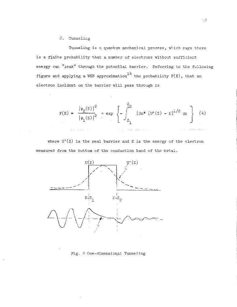
2. Tunneling
Tunneling i s a quantum mechanical process , which says t h e r e
i s a f i n i t e p r o b a b i l i t y t h a t a number of e l e c t r o n s without s u f f i c i e n t
energy can "leak" through t h e p o t e n t i a l b a r r i e r . Refer r ing t o t h e fol lowing
1 4 f i g u r e and applying a WKB approximation t h e p r o b a b i l i t y P(E), t h a t an
e l e c t r o n i n c i d e n t on t h e b a r r i e r w i l l pass through i s
= exp
where U'CZ) i s t h e r e a l b a r r i e r and E i s t h e energy o f t h e e l e c t r o n
measured from t h e bottom o f t h e conduction band of t h e me ta l .
F ig . 2 One-dimensioqal Tunneling
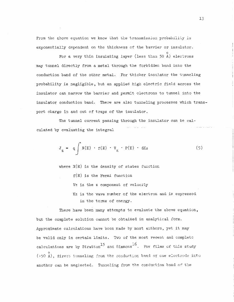
From t h e above equat ion we know t h a t t h e t ransmiss ion p r o b a b i l i t y i s
exponent ia l ly dependent on t h e th i ckness of t h e b a r r i e r o r i n s u l a t o r . 0
For a very t h i n i n s u l a t i n g l a y e r ( l e s s t han 50 A ) e l e c t r o n s
may t u n n e l d i r e c t l y from a metal through t h e forbidden band i n t o t h e
conduction band o f t h e o the r metal . For t h i c k e r i n s u l a t o r t h e tunne l ing
p r ~ b a b i l i t y i s n e g l i g i b l e , bu t an appl ied high e l e c t r i c f i e l d ac ros s t h e
i n s u l a t o r can narrow t h e b a r r i e r and permit e l e c t r o n s t o t unne l i n t o t h e
i n s u l a t o r conduction band. There a r e a l s o tunne l ing processes which t r a n s -
p o r t charge i n and out o f t r a p s o f t h e i n s u l a t o r .
The t u n n e l cu r r en t pas s ing through t h e i n s u l a t o r can be ca l -
cu l a t ed by eva lua t ing t h e i n t e g r a l
where N(E) i s t h e dens i ty of s t a t e s func t ion
f ( E ) i s t h e Fermi func t ion
Vz i s t h e z component of v e l o c i t y
Kz i s t h e wave number of t h e e l e c t r o n and i s expressed
i n t h e terms o f energy.
There have been many a t tempts t o eva lua t e t h e above equat ion ,
but t h e complete s o l u t i o n cannot be obta ined i n a n a l y t i c a l form,
Approximate c a l c u l a t i o n s have been made by most au tho r s , y e t it may
be v a l i d only i n c e r t a i n l i m i t s . Two of t h e most recent and complete
c a l c u l a t i o n s a r e by ~ t r a t t o n ' ~ and S i m o n s l 6 . For f i lms of t h i s s tudy 0
('50 A ) d i r e c t t unne l ing from t h e conduction band of one e l ec t rode i n t o
another can be neg lec t ed , Tunneling from t h e conduction band of t h e
e l e c t r o d e i n t o t h e conduction band of t h e i n s u l a t o r due t o narrowing of
t h e b a r r i e r by t h e e l e c t r i c - f i e l d , however, i s p o s s i b l e , Simmons g ives
t h e express ion f o r t h i s condi t ion a s 1 9
J = 2.2q E
exp - 7
3 2 [ 8n(2m)1/2(m)3/2 i
Although t h e r e a r e some incons i s t enc i e s which i n d i c a t e s an inadequacy
o f t h e i d e a l i z e d t h e o r e t i c a l model (and t h e d i f f i c u l i t i e s o f t h e c o n t r o l l i n g
t h e junc t ion f a b r i c a t i o n t echn iques ) , t h e main f e a t u r e s o f t h e t h e o r e t i c a l
7 analyses have been corroborated
Recent ly , t unne l ing s t u d i e s have been extended t o Met a l - In su la to r -
Semiconductor junctions7'17'18* Chang , S t i l e s , and Esairi have given
t h e o r e t i c a l cur ren t -vol tage express ions , i n p a r t i c u l a r , f o r t h e case
when t h e semiconductor i s a degenerate p t ype . Wilmsen i n v e s t i g a t e d
tunne l ing between a meta l and s i l i c o n sepa ra t ed by a t h i n i n s u l a t i n g
polymer and developed a model descr ib ing t h e current-vol tage c h a r a c t e r i s t i c s .
The model shows t h a t t h e e l e c t r i c f i e l d i n t h e i n s u l a t o r c o n t r o l s t h e MIS
cu r ren t while t h e charge d i s t r i b u t i o n i n t h e s i l i c o n determines t h e
i n s u l a t o r f i e l d . Wilmsen a l s o ind ica t ed t h a t t h e mechanisms f o r M I M
and MIS tunne l ing a r e q u i t e s i m i l a r and an asymmetric s a t u r a t i o n of
t h e MIS tunne l ing was caused by t h e forrnation of a deple t ion l a y e r on
t h e semiconductor which formed a f t e r completely charging the su r f ace
s t a t e s .
When su r f ace e f f e c t s a r e not considered, Wilmsen gave t'he

t unne l ing cu r ren t expression a s
2.rrC10kT J x = J o P { - v - v 2 Sinh P l O ( V - ( 7 )
s in (nClok~) J i 1 Where b12 and C i O a r e sma l l e r f o r MIS than f o r M I M ,
and V accounted empi r i ca l ly f o r t h e semiconductor energy gap. G
The cons t an t s b and C a r e func t ions o f t h e phys i ca l parameters o f 12 10
t h e i n s u l a t o r , i . e o , d i e l e c t r i c cons t an t , t h i ckness and e f f e c t i v e mass,
-2 O f p a r t i c u l a r importance i s t h e dependence of b and C10 upon L a.nd
12
L - ~ r e s p e c t i v e l y , where L i s t h e th i ckness of t h e i n s u l a t o r .
3. Poole Frenkel E f f e c t
Real i n s u l a t o r s have l a r g e q u a n t i t i e s o f imperfec t ions .
Each imperfec t ion in t roduces one o r more l o c a l i z e d energy s t a t e s which
can be donor o r acceptor type . High concent ra t ion of fmperfect ions can
change t h e conduction phenomena i n th in- f i lm i n s u l a t o r s . S t a t e s which
a r e empty i n equi l ibr ium may t r a p f r e e excess c a r r i e r s , removing them
from t h e conduction process . Local ized imperfect ions a l s o can s c a t t e r
f r e e charge c a r r i e r s , thereby reducing t h e i r mob i l i t y .
By extending t h e model used t o exp la in t h e conduct iv i ty of
semiconductors, a model s u i t a b l e f o r expla in ing t h e c o n d ~ c t ~ i v i t y of
i n s u l a t o r s w i t h t r a p s can be The energy band s t r u c t u r e
of one o f t h e s e models i s shown i n Figure 3.

Bottom o f Conduct ion Band
- -- - - - - 2 - - - - - - - - - - - - - t
- . ---. .+ . ----- . ---- - . Fermi Level
Fig. 3 I n I n s u l a t o r Band Model, E and E a r e energy t d
l e v e l s f o r t r a p s and donors
By equat ing t h e number of e l e c t r o n s miss ing from donor cen te r s t o t h e
number o f occupied t r a p s and assuming t h e number of e l e c t r o n s i n t h e
conduction band can be neglec ted , t h e p o s i t i o n of a " ~ e r m i " l e v e l can
be loca t ed . Let Nt and N be t r a p s p e r cmJ and donors p e r cm3 respectively. d
Then,
from which,
A t zero b i a s o r low vol tage t h e concent ra t ion of' f r e e e l e c t r o n s i s due
t o t h e thermal energy of t h e i n s u l a t o r , The number of f r e e e l e c t r o n s n ,

i s given by
where Nc i s t h e e f f e c t i v e dens i ty o f s t a t e s i n t h e i n s u l a t o r .
Reca l l t h e express ion f o r t h e conduct iv i ty o f a m a t e r i a l i s
a = nqy ohm-cm (10)
Where n i s t h e concent ra t ion of f r e e c a r r i e r s ,
p i s t h e mob i l i t y o f t h e c a r r i e r , and
q i s t h e charge on t h e c a r r i e r
Therefore , t h e conduct iv i ty o f t h e imperfect i n s u l a t o r a low f i e l d i s 21,22
and t h e cu r r en t dens i ty i s
where Vb i s t h e b i a s vol tage and
L i s t h e th i ckness of t h e i n s u l a t o r ,

A t high f i e l d s , t h e f i e l d i n t e r a c t s with t h e t r a p b a r r i e r i n
t h e i n s u l a t o r and lowering it by an amount of
vhere E = - i s t h e app l i ed f i e l d and L
K i s t h e r e l a t i v e d i e l e c t r i c cons t an t ,
Refeming t o f i g u r e 4, t h i s f i e l d lowering of t h e b a r r i e r i s known as t h e
Poole-Frenkel e f f e c t . It r e s u l t s i n t h e conduct iv i ty be ing field-dependent
Bottom o f Conduct ion Band
Fig 4. Mechanism of Poole-Frenkel E f fec t
s i n c e it d r a s t i c a l l y i nc reases t h e c a r r i e r concent ra t ion . The number
of f r e e e l e c t r o n s i n t h e conduction band inc reases t o 2 1
and t h e conduct iv i ty becomes
a = o o exp ( B ~ ~ E ~ / ~ / ~ ~ T )
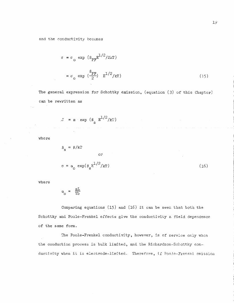
The gene ra l express ion f o r Schottky emission, (equat ion ( 3) o f t h i s Chapter)
can be r e w r i t t e n a s
J = u exp ( B s E ~ / ~ / ~ T )
where
where
Comparing equat ions ( 1 5 ) and (16) it can be seen t h a t bo th t h e
Schottky and Poole-Frenkel e f f e c t s g ive t h e conduct iv i ty a f i e l d dependence
of t h e sane form,
The Poole-Frenkel conduc t iv i ty , however, i s of s e r v i c e only when
t h e conduction process i s bulk l i m i t e d , and t h e Richardson-Schottky con-
d u c t i v i t y when it i s e l ec t rode - l imi t ed , Therefore, if Poole-Frenkel emisslon

dominates, t h e cu r r en t c h a r a c t e r i s t i c s a r e i n s e n s i t i v e t o changes i n
p o l a r i t y and t h e t y p e of meta l used a s e l e c t r o d e s . I f $chot tky emission
dominates, a l a r g e d i f f e r e n c e i n cur ren t magnitude a t equa l bu t oppos i te
f i e l d s r e s u l t s when meta l wi th d i f f e r e n t work func t ions form t h e e l e c t r o d e s ,
The t h e o r e t i c a l va lues of Bs and BpF can be c a l c u l a t e d accu ra t e ly
provided t h a t t h e high-frequency d i e l e c t r i c cons tan t f o r t h e i n s u l a t o r i s
known. Thus, one can t h e o r e t i c a l l y d i f f e r e n t i a t e between t h e two types of
conduct iv i ty from t h e i r d i f f e r e n t r a t e s of change o f conduct iv i ty wi th
1 / 2 f i e l d s t r e n g t h , A p l o t of I n a versus E / k ~ r e s u l t s i n a s t r a i g h t l i n e
of s lope Bs o r BpF. This experiment a l l y determined s lope can be compared
wi th t h e t h e o r e t i c a l l y c a l c u l a t e d Bs and BpF t o h e l p determine which
mechanism i s t h e dominant one.
B. $emiconductor Surf ace S t a t e s and D-C Current S a t u r a t i o n -- ,
The complete d e s c r i p t i o n of t h e V - I c h a r a c t e r i s t i c involves t h e
i n t e r f a c e between a non-c rys t a l l i ne polymer and t h e s i n g l e c r y s t a l bulk
s i l i c o n . The theo ry must inc lude su r f ace s t a t e e f f e c t s which modify t h e
bulk t h e o r i e s of conduct iv i ty and capaci tance and t a k e i n t o account
charge t r a n s p o r t not u sua l ly t r e a t e d i n t h e MOS capac i to r t heo ry .
The e l e c t r o n behavior i n a c r y s t a l can b e s t be descr ibed i n
terms of wave mechanics. The d i f f e r e n t i a l equat ion , whose s o l u t i o n s a r e
wave-like func t ions , i s t h e Schroedinger equat ion. I n a one dimensional
c r y s t a l l a t t i c e t h e p o t e n t i a l energy of an e l e c t r o n can be approximated
by a pe r iod ic a r r a y o f square we l l s - t h e Kronig-Penney model, Because
of te rmina t ion o f t h e p e r i o d i c i t y a t t h e sur face o f an a c t u a l c r y s t a l ,

Tamm proposed a modified Kronig-Penney model energy diagram as shown i n
Figure 523. The Schrodinger equat ion f o r an e l e c t r o n moving i n such
p o t e n t i a l i s :
Figure 5 P o t e n t i a l Energy of An ,F)lectron wi th in
Pe r iod ic Crys t a l L a t t i c e
a) Schematic r ep re sen ta t ion of a c t u a l condi t ions .
b ) $quare-well approximation employed by T m .
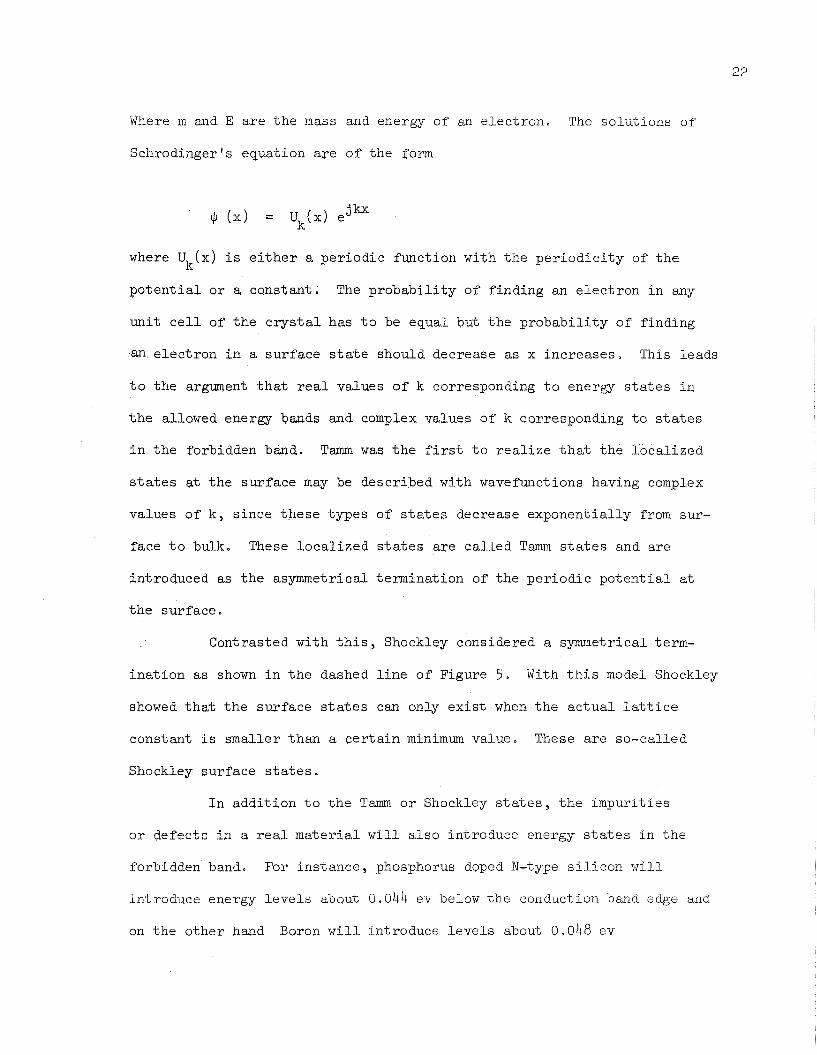
Where m and E a r e t h e mass and energy of an e l e c t r o n , The so lu t ions of
Schrodinger 's equat ion a r e o f t h e form
where U ( x ) i s e i t h e r a p e r i o d i c func t ion wi th t h e p e r i o d i c i t y of t h e k
p o t e n t i a l o r a cons tan t . The p r o b a b i l i t y o f f i nd ing an e l e c t r o n i n any
u n i t c e l l of t h e c r y s t a l has t o be equal but t h e p r o b a b i l i t y o f f ind ing
an e l e c t r o n i n a su r f ace s t a t e should decrease a s x i n c r e a s e s , This leads
t o t h e argument t h a t r e a l values o f k corresponding t o energy s t a t e s i n
t h e allowed energy bands and complex va lues o f k corresponding t o s t a t e s
i n t h e forbidden band. Tamm was t h e f i r s t t o r e a l i z e t h a t t h e l o c a l i z e d
s t a t e s a t t h e su r f ace may be descr ibed wi th wavefunctions having complex
values of k , s i n c e t h e s e types of s t a t e s decrease exponen t i a l l y from sur-
face t o bulk. These l o c a l i z e d s t a t e s a r e c a l l e d Tamm s t a t e s and a r e
introduced a s t h e asymmetriaal t e rmina t ion of t h e p e r i o d i c p o t e n t i a l a t
t h e su r f ace .
Contrasted wi th t h i s , Shockley considered a symmetrical term-
i n a t i o n a s shown i n t h e dashed l i n e o f Figure $. With t h i s model Shockley
showed t h a t t h e su r f ace s t a t e s can only e x i s t when t h e a c t u a l l a t t i c e
cons tan t i s sma l l e r t han a c e r t a i n minimum value , These a r e so-ca l led
Shockley su r f ace s t a t e s .
I n a d d i t i o n t o t h e Tamm o r Shockley s t a t e s , t h e impuri t , ies
o r de fec t s i n a r e a l m a t e r i a l w i l l a l s o in t roduce energy s t a t e s i n t h e
forbidden band. For i n s t a n c e , phosphorus doped I?-type s i l i c o n w i l l
in t roduce energy l e v e l s about 0,044 ev below the conduction band edge and
on t h e o t h e r hand Boron w i l l in t roduce l e v e l s about 0.048 ev

24 above t h e valence/ band edge I n many cases , t h e semiconductor sur face
i s covered with a l a y e r of fore ign ma te r i a l , such a s an oxide, as e i t h e r
an acc iden ta l o r d e l i b e r a t e r e s u l t of t h e prepara t ion procedure. S t a t e s
l y i n g wi th in o r on t h e outer sur face of such a l a y e r a r e a l s o commonly c a l l e d
sur face s t a t e s , even though they do not o r i g i n a t e i n t h e semiconductor
i t s e l f 2 5 . There i s no genera l mathematic so lu t ion f o r ) (x) which can be
used on t h e MPS s t r u c t u r e . It i s recognized, however, a l l t h e s e c l a s ses
of s t a t e s may a c t a s t r a p s , recombination cen te r s , o r both , and thus
may make t h e semiconductor sur face "metal l ic" o r change many p roper t i e s
of semiconducting devices, A phenomenologic theory i s a l l t h a t can be
o f fe red a t t h i s t ime.
The changing of DC conduction mechanisms of MIS devices due
t o i n t e r f a c e s t a t e dens i ty i s of s p e c i a l i n t e r e s t t o t h i s experiment
and study, s ince it i s t h e p r i n c i p l e of t h e MPS d i g i t a l t ransducer .
Wilmsen proposed current s a t u r a t i o n of t h e MPS device i n reverse b iased
condit ion due t o erhaus t ion of sur face s t a t e changes. wilmsen9 s t a t e d
t h a t t h e s i l i c o n surface s t a t e s cause an N-shift i n t h e sur face energy,
The surface s t a t e s a r e f i l l e d up t o t h e Fermi l e v e l . When negative
vol tage i s appl ied t o the meta l f i e l d p l a t e , mobile e l ec t rons a re removed
from t h e sur face s t a t e s . This continues u n t i l t h e supply of e l ec t rons
from t h e surface s t a t e s i s exhausted. When negat ive b i a s vol tage i s
f u r t h e r increased a sur face accumulation o r deple t ion region w i l l be
formed depending upon t h e type of semiconductor. When p o s i t i v e vol tage i s
appl ied t o t h e metal f i e l d p l a t e , mobile e l ec t rons a r e "driven" i n t o t h e

su r f ace s t a t e s and t h i s w i l l continue u n t i l a l l t h e su r f ace s t a t e s a r e
f i l l e d up. Again a su r f ace accumulation o r dep le t ion region w i l l be formed
when t h e b i a s vo l t age i s f 'ur ther increased . The important po in t i s t h a t
t h e e l e c t r i c f i e l d was assumed t o be e n t i r e l y w i th in t h e i n s u l a t o r u n t i l
t h e su r f ace s t a t e s a r e exhausted. Recent experimental evidence has l e d
t o a r e l a x a t i o n of t h i s requirement.
I n a reverse-biased dep le t ion reg ion , f o r r eve r se b i a s
V >> kT/q, t h e concent ra t ion of c a r r i e r s i s reduced we l l below t h e i r r
equi l ibr ium concent r a t i o n . The r a t e o f genera t ion of e lectron-hole
p a i r s i n such a s i t u a t i o n can be obta ined from t h e equat ions f o r e l ec t ron -
ho le p a i r recombination-generation i n t h e bulk o f semiconductor 30,31 by
l e t t i n g p , n << n . This l eads t o i
where T i s t h e e f f e c t i v e l i f e t i m e wi th in a reverse-biased dep le t ion region 0
and i s given by
Op 5 "n = capture c ross -sec t ion of ho les and e l e c t r o n s
v th = thermal v e l o c i t y of c a r r i e r s
Nt = concent ra t ion of bulk recombination-generation cen te r s p e r u n i t volume
Et = energy l e v e l of recombination-generation cen te r
i = e l e c t r o n energy a t t h e i n t r i n s i c Fermi Level ,

The genera t ion c u r r e n t , ~~rhieh is extremely important i n
a n a l y s i s t h e I - V c h a r a c t e r i s t i c s of MPS devices i n reverse b i a s condi t ion
i s p ropor t iona l t o t h e genera t ion r a t e U. Another f a c t o r which a f f e c t s
t h e genera t ion cu r r en t i s t h e deple t ion l a y e r width. For a P-N Junct ion
t h i s width i s expressed a s
where $T i s r e f e r r e d t o a s t h e b u i l t - i n vol tage $ of b
a p-n junc t ion
I n t h e MIS capac i to r s t r u c t u r e , i f a s m a l l r everse b i a s vo l t age
i s appl ied , a dep le t ion reg ion tends t o form, The charge pe r u n i t a r e a
contained i n t h i s dep le t ion region i s Q = - qNaW (assume N-type ~ i ) . s
I f t h e r eve r se b i a s vol tage i s f u r t h e r increased , a very narrow inve r s ion
l a y e r may s t a r t t o form. I n an equi l ibr ium case , t h a t i s no D-C cu r r en t
flow through t h e c a p a c i t o r , t h e width o f t h e dep le t ion l a y e r reaches
a maximum. Thus, under s t rong inve r s ion condi t ions t h e charge p e r u n i t
a r e a induced t h e semiconductor w i l l be given a s
where Q i s charge i n t h e inve r s ion l a y e r . An important po in t i s t h a t i n
a smal l i nc rease i n dep le t ion region width may r e s u l t i n a very l a r g e
inc rease i n t h e charge contained wi th in t h e inve r s ion l a y e r .
I n t h e MPS devices , curren t can flow through t h e polymer, t h e r e f o r e ,
a non-equilibrium s i t u a t i o n e x i s t s vhen t h e device i s reverse b i a sed*
The dep le t ion l a y e r width may never reach a maximum value , bu t would inc rease
very slowly when b i a s vol tage i s cont inuously increased .
Wilmsen observed t h e cu r r en t s a t u r a t i o n o f MPS capac i to r s i n
t h e r eve r se b i a s e d condi t ion and explained it a s f i e l d pene t r a t ion i n t o
t h e semiconductor when su r f ace s t a t e s have been exhausted. Therefore , t h e
su r f ace s t a t e s a c t l i k e a " t r a n s i t i o n switch"; before iti exhausted it
s h i e l d s t h e semiconductor su r f ace and makes t h e semiconductor behave l i k e
a "metal". The cu r ren t passing through t h e MPS device w i l l be i nc reas ing
exponen t i a l l y wi th b i a s vol tage j u s t l i k e cu r r en t conducting i n MPM devices ,
Af t e r t h e su r f ace s t a t e s have been exhausted, t h e "metal" behaves l i k e
semiconductor aga in . The rea f t e r e l e c t r i c f i e l d l i n e s te rmina te on t h e
charges i n t h e dep le t ion reg ion , It i s now apparent t h i s explana t ion can
be modified by i n c l u s i o n of Qin i n t h e model. The impact o f such a model
on t h e r e a l i z a t i o n of a d i g i t a l device behavior would be very b e n e f i c i a l
s ince it would provide a r a t i o n a l means t o r e l a t e phys i ca l behavior a t
t h e "break" t o parameters which may be c o n t r o l l e d ,

CHAPTER 111
EXPERIMENTAL PROCEDURES
A. Sample P repa ra t ion
Previous research on M I M o r MOS junc t ions showed t h a t t h e device
performance and y i e l d s were extremely s e n s i t i v e t o su r f ace p repa ra t ion and
smoothness. For t h i s reason two ca t egor i e s o f s i l i c o n wafers were used i n t h e
experiment.
1. Commerically a v a i l a b l e mechanical ly pol i shed medium r e s i s t i v i t y
both P and N t y p e s i l i c o n wafer ( % 10 ohm-cm, from Texas ~ n s t r u m e n t s ) .
2 . Mechanically lapped and chemically po l i shed N t y p e s i l i c o n
wafers prepared i n t h e E lec t ron ic Ma te r i a l s Research Laboratory o f The
Univers i ty of Texas ( % 30 ohm-cm t o % 250 ohm-cm) . The lapping and
po l i sh ing process f o r group two wafers a r e :
a ) The wafer p repa ra t ion begins wi th a s i n g l e c r y s t a l s i l i c o n
boule cut i n t o 25 m i l s l i c e s wi th a diamond wheel.
b ) The 25 m i l s l i c e i s lapped wi th # 240 alumina g r i t t o remove
t h e saw damage. The #240 g r i t i s removed by r i n s i n g i n deionized water
and by u l t r a - s o n i c a l l y cleaning i n methyl a l coho l ,
c ) S t e p B i s repea ted wi th #400, #600 and 5 micron g r i t s t o
o b t a i n a s c ra t ch - f r ee su r f ace p r i o r t o chemical po l i sh ing ,
d ) The u l t r a - s o n i c a l l y c lean wafer i s etched w i t h . CP-4
about 70 seconds. During t h i s e t ch ing process t h e wafer should be
a g i t a t e d a l l t h e t ime i n t h e breaker . The e t ch ing i s s topped by quick ly
adding deionized water t o t h e CP-4 A smooth mi r ro r su r f ace should be
achieved.

Both groups of t h e wafers should have t h e i d e n t i c a l and s t r i c t
c leaning procedures a s fo l lows:
a ) Clean a l l glassware and o t h e r hardware t o be used i n t h e
c leaning process with non-ioni c de te rgent and g l a s s cleaning s o l u t i o n ,
b ) Scrub t h e s i l i c o n wafer wi th t h e non-ionic d e t e r g e n t ,
c ) Rinse o f f t h e de te rgent wi th deionized water ,
d ) p l ace t h e wafer i n a 50 m l beaker and cover with f r e s h , d ry
methyl a l coho l ,
e ) U l t r a - son ica l ly a g i t a t e f o r 30 seconds,
f) Pour o f f t h e methyl a l coho l and cover with t r i c h l o r o e t h y l e n e ,
g ) B o i l i n t h e t r i c h l o r o e t h y l e n e f o r one minute,
h ) Pour o f f t h e t r i c h l o r o e t h y l e n e and repea t s t e p g,
i ) Pour o f f t h e t r i c h l o r o e t h y l e n e and f lu sh wi th deionized
water f i v e t imes ,
' j ) Place t h e wafer i n hydro f luo r i c a c i d f o r 30 seconds,
k) Flush with deionized water seven t imes ,
1) cover t h e wafer with methyl a l coho l ,
m ) steam t h e wafer wi th b o i l i n g t r i c h l o r o e t h y l e n e f o r 30 seconds
and t r a n s f e r t o t h e vacuum chamber a s quick ly a s poss ib l e .
B. Back Side Contact -- Since h igh r e s i s t i v i t y s i l i c o n (10 ohm-cm t o 250 ohm-cm) i s
used i n making t h e MPS device , t h i s w i l l i n e v i t a b l y in t roduce problems
of prevent ing r e c t i f y i n g con tac t s . Three techniques have been adopted t o
i n s u r e good ohmic con tac t s :

a ) s i l v e r depos i t ion : Ohmic contac t can be made t o P-type
m a t e r i a l when t h e e f f e c t i v e work func t ion of t h e semiconductor i s l e s s
t h a n t h e work func t ion of meta l . For 1 0 ohm-cm p type s i l i c o n t h e e f f e c t i v e
work func t ion i s 4.2 e v and f o r s i l v e r t h e work func t ion i s 4.73 ev. There-
f o r e , ohmic contac t can be in su red when t h e s i l v e r i s evaporated on t h e
p t y p e s i l i c o n wafer. This s i l v e r depos i t i on i s usua l ly made be fo re
polymerizat ion t a k e s p lace .
b ) E l e c t r o l e s s Nickel P l a t i n g : I n e l e c t r o l e s s p l a t i n g an
e l e c t r o n in te rchange has t o t a k e p l ace between two chemical spec i e s . The
e l e c t r o l e s s n i c k e l p l a t i n g involves t h e c a t a l y t i c reduct ion of n i c k e l ions
by sodium hypophosphite. The hypophosphite i on g ives up e l e c t r o n s and
becomes phosphi te i o n , and t h e n i c k e l i o n rece ives t h e e l e c t r o n s and
depos i t s as m e t a l l i c n i cke l . A t y p i c a l ba th f o r use on germanium o r
s i l i c o n may be made a s fol lows : 27
g r a m s / l i t e r Nickel ch lo r ide ( ~ i C 1 ~ . 6 ~ ~ 0 ) . . . . . . . . . . . . . 30
Sodium hypophosphite (NaH2~02 . ~ ~ 0 ) . . . . . . . . . . 10
~mmonium c i t r a t e [ (NH ) HC H o 1 . . . . . . . . . . . . 65 4 2 6 5 7
Ammonium ch lo r ide ( N H ~ c ~ ) . . . . . . . . . . . . . . . 50
F i l t e r
Add ammonium hydroxide ( N H ~ O H ) u n t i l t h e s o l u t i o n t u r n s from green t o
b lue . This i s p a r t i c u l a r l y u s e f u l on s i l i c o n , because s o r t - s o l d e r
0 connection can be made t o it a t temperature below 200 C , For 10 ohm-cm
N-type s i l i c o n , one e l e c t r o l e s s p l a t i n g i s s u f f i c i e n t f o r making ohmic
contac t For h ighe r r e s i s t i v i t y materf a l , improvement i s made by a l loy ing
0 t h e n i c k e l i n t o t h e s i l i c o n a t temperatures of 800 t o 900 C, I n t h e

l a t t e r case a second n i c k e l p l a t e i s necessary, When t h i s technique i s
used, t h e wafers a r e u sua l ly e l e c t r o l e s s p l a t e d before t h e c leaning p roces s ,
c ) An Indium Gallium p a s t e o r a Mercury-Indium-Lead p a s t e
smeared onto t h e back s i d e of s i l i c o n wafer o f f e r s another way o f making
ohmic c o n t a c t s . Cleaness of t h e wafer i s t h e e s s e n t i a l f a c t o r f o r success
~f t h i s method. Therefore, t h e p a s t e i s appl ied t o t h e wafer immediately
a f t e r t h e c leaning process ,
C , Polymer Formation
The formation method and c h a r a c t e r i s t i c s of t h e i n s u l a t i n g
t h i n polymer have been descr ibed by Ennos and ~ h r i s t ~ ~ ~ ' ~ ~ ~ The polymer-
i z a t i o n process begins when low energy ( 2350 ev ) e l e c t r o n s break t h e bonds
between r a d i c a l s of an organic molecule. I n t h i s experiment, t h e Dow
Corning 704 d i f f u s i o n pump o i l used i n t h e vacuum systems served a s a
source of t h e organic molecules. An RCA 902 A cathode-ray-tube wi th t h e
f a c e p o r t i o n of t h e tube removed i s used as t h e supply of e l e c t r o n s f o r t h e
polymerizat ion, The schematic diagram f o r t h e cathode r ay tube c i r c u i t
i s shown i n f i g u r e 10 .
A t h r e e s t a t i o n set-up and a r o t a r y sample holder as descr ibed
by ~ i l m s e n ~ a r e i n s t a l l e d i n t h e b e l l jar of t h e vacuum system. The sample
ho lde r w i l l f i r s t r o t a t e t h e sample t o t h e s t a t i o n , where t h e e l e c t r o n
beam o f t h e CRT w i l l h i t t h e f i lm of o i l molecules on t h e sur face sample
and t h e polymerizat ion process w i l l t a k e p l ace , The growth r a t e of t h e
polymer i s a func t ion of t h e dens i ty of t h e e l e c t r o n beam, t h e p re s su re
i n t h e vacuum system, and t h e dura t ion of time which t h e system has been

1, Subs t r a t e
2 Polymer
3. Elec t ron Beam
4. Deflec t ion P l a t e s
5 , Acce lera t ion Anode
6. Focusing Anode
7. Cathode
8. Heater
Fig. 6 Cathode Ray Tube C i r c u i t
pumped down. For one and a h a l f hours pump-down ( t h e vacuum system
reaches 5 x l o m 5 t o r r and a beam cu r ren t dens i ty of 4 micro-Amp/cm2, t h e 0
growth r a t e i s about 1.8 A/minute. By t h e polymerizat ion s t a t i o n i s a
small c r u c i b l e 1 . 5 cm i n diameter f u l l e d with D.C. 704 o i l , When hea ted
0 up t o 60 C f o r one hour before polymerizat ion, t h i s c ruc ib l e would supply
an e x t r a source of pump o i l f o r polymerizat ion and inc rease t h e growth 0
r a t e t o 2 . 8 A/mina
D. E l e c t r o p l a t e Deposit ion
Af t e r t h e polymer been formed on t h e s i l i c o n s u b s t r a t e , t h e sample
was r o t a t e d t o t h e f i r s t meta l depos i t ion p o s i t i o n , where t h r e e aluminum
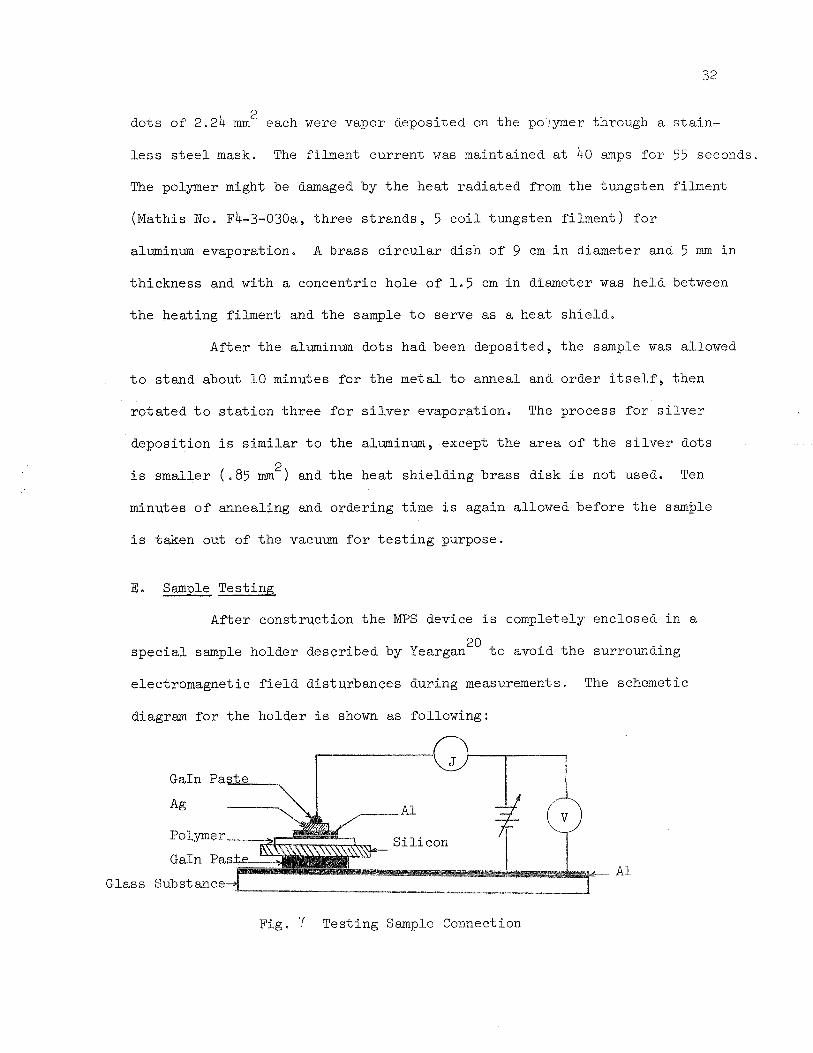
2 do t s of' 2.24 mm each were vapor deposi ted on t h e polymer through a s t a i n -
l e s s s t e e l mask. The f i lment cu r r en t was maintained a t 40 amps f o r 55 seconds,
The polymer might be damaged by t h e hea t r ad i a t ed from t h e tungs t en f i lment
a at his No. ~4-3-030a, t h r e e s t r a n d s , 5 c o i l tungs ten f i lmen t ) f o r
aluminum evaporat ion. A b r a s s c i r c u l a r d i sh of 9 cm i n diameter and 5 mm i n
t h i ckness and wi th a concent r ic ho le of 1 . 5 cm i n diameter w a s h e l d between
t h e hea t ing f i lment and t h e sample t o serve a s a hea t s h i e l d .
Af t e r t h e aluminum dots had been deposi ted, t h e sample was allowed
t o s t and about 1 0 minutes f o r t h e meta l t o anneal and o rde r i t s e l f , t hen
r o t a t e d t o s t a t i o n t h r e e f o r s i l v e r evaporat ion. The process f o r s i l v e r
depos i t i on i s s i m i l a r t o t h e aluminum, except t h e a r e a of t h e s i l v e r do t s
2 i s smaller ( .85 rnm ) and t h e h e a t s h i e l d i n g b ra s s d i s k i s not used. Ten
minutes o f anneal ing and order ing t ime i s again allowed be fo re t h e sample
i s taken out of t h e vacuum f o r t e s t i n g purpose.
E. Sample Testin&
Af ter cons t ruc t ion t h e MPS device i s completely enclosed i n a
s p e c i a l sample ho lde r descr ibed by yearganeO t o avoid t h e surrounding
e lec t romagnet ic f i e l d d is turbances dur ing measurements, The schemetic
diagram Tor t h e ho lde r i s shown a s fol lowing:
Glass
GaIn Pa
Ag
Polymer
GaIn Pa
lbstance
F ig . 7 Test ing Sample Connection

The capaci tance measurements of t h e device were made on a General Radio
1615 A capaci tance br idge at 1 Kc. The th i ckness of t h e polymer were
obta ined through t h e r e l a t i o n ,
K E ~ A d =
C (neg lec t ing f r i n g i n g )
where K = r e l a t i v e d i e l e c t r i c cons t an t ,
A = t h e a r e a o f t h e a l m i n m f i l e d p l a t e ,
C = t h e capaci tance o f t h e MPS device,
A Hewlett-Packard 425 A micromicro-ammeter and a Hewlett-Packard 413 A dc
vol tmeter measure t h e cu r r en t and v ~ l t a g e r e s p e c t i v e l y ,
CHAPTER I V
EXPERIMENTAL RESULTS
For a pe r iod of t e n months, more than e ighty samples have been
made f o r t h i s r e sea rch p r o j e c t . I n t h e e a r l y s t a g e , Ag-polymer-Si
devices were made. S i l v e r e l e c t r o d e s were used because t h e Ga-In e u t e c t i c
"blob" wets it s o we l l during measuring process , good e l e c t r i c a l contac t
i s always ensured. However, a l a r g e f r a c t i o n of samples were sho r t ed o u t ,
A group of samples made wi th t i n , l e a d and n i c k e l t o p e l e c t r o d e s were a l s o
sho r t ed . Aluminum e l ec t rodes can always g ive p o s i t i v e r e s u l t s , but t h e
Ga-In does not t e n d t o wet t h e aluminum and good e l e c t r i c a l contac t i s
extremely d i f f i c u l t . Therefore, an a d d i t i o n a l f a b r i c a t i o n process i s necessary t o
ensure good e l e c t r i c a l contac t and prevent s h o r t c i rcui t r . A new
evaporat ion mask was cu t and s i l v e r do t s , smal le r i n diameter t han t h e
aluminum do t s , were l a i d over t h e aluminum e l ec t rodes . With t h i s config-
u r a t i o n , aluminum was contiguous t o t h e polymer and assured a h igh sample
y i e l d while $ i l v e r was exposed i n o r d e r t o make good contac t wi th t h e
GaIn blob.
I n t h e second p e r i o d of t h e experiment succes s fu l samples,
wi th reproduceable I - V c h a r a c t e r i s t i c , capaci tance reading , and low
d i s s i p a t i o n facCor , were cont inuously made i n t h e l a b o r a t o r y , The
th i ckness of polymer determined by capaci tance measurement had been checked
wi th e l l i p somete r measurement, it showed l e s s than 10% of disagreement .
Low d i s s i p a t i o n f a c t o r ( i n t h e range of 0 ,001 t o 0,04 a t 1 K C ) ~ n d i c a t e s
good ohmic contac t t o t h e s i l i c o n wafers had been made. Most samples
3 4

were made on mechanically po l i shed N-type 10Q-cm s i l i c o n , a few were made
on P-type o r of h igher r e s i s t i v i t y (70-113Q-cm) wafers , The th i ckness 0
o f polymer f o r t hose samples were around 150 A.
No d i s t i ngu i sh ing s a t u r a t i o n was observed f o r e i t h e r p o l a r i t y
however. Two samples made on 80Q cm N-type s i l i c o n showed t h e tendencies
of s a t u r a t i o n but t h e cu r r en t never l e v e l e d o f f . From t h e s e r e s u l t s , two
conclusions have been drawn:
1. Chemically po l i shed s i l i c o n wafers may have t o be used, s i n c e
t h e mechanically prepared su r f ace might have much h ighe r s u r f a c e s t a t e
dens i ty simply because of mechanical damage of t h e su r f ace during the
lapping and po l i sh ing processes .
2. Thinner polymer i s p r e f e r r e d , because it w i l l decrease t h e
s a t u r a t i o n vo l t age .
Samples were made wi th chemically pol i shed s i l i c o n wafers , A
h ighe r f r a c t i o n of samples showed t h e s a t u r a t i o n c h a r a c t e r i s t i c s
demonstrating a cause-and-effect r e l a t i o n had been e s t a b l i s h e d between
su r f ace p repa ra t ion and onset of s a t u r a t i o n f o r r eve r se b i a s e d MPS devices ,
I n t h e fo l lowing s e c t i o n s t h e charge t r a n s p o r t mechanisms i n
polymer and curves demonstrating cur ren t s a t u r a t i o n , a r e d iscussed ,
A, Conduction P r o p e r t i e s of Polymer
The charge t r a n s p o r t mechanisms i n t h i n f i lm polymers may b e s t
be observed and understood by making MPM capac i to r s . The reason i s i n
MPS devices , t h e f i e l d p e n e t r a t i o n i n t o t h e semiconduetor and t h e ex i s t ance
of su r f ace s t a t e s i n t h e polymer-semiconductor i n t e r f a c e complicate t h e

problems.
Figure 8 shows a t y p i c a l behavior o f t h e cu r r en t wi th b i a s of
an MPM capac i to r . The I n J vs v1I2 i s a very s t r a i g h t l i n e , wi th a
changing s lope at h ighe r b i a s . The s t r a i g h t l i n e c h a r a c t e r i s t i c i n d i c a t e s
t h a t it i s Schot tky emission o r Poole-Frenkel e f f e c t , The changing of
Slope sugges ts more t h a n one mechanisms may be involved. Theore t i ca l ly ,
one can d i f f e r e n t i a t e q u i t e r e a d i l y between Schottky emission and t h e Poole-
Frenkel e f f e c t from t h e i r d i f f e r e n t r a t e s o f change o f conduct iv i ty wi th
f i e l d s t r e n g t h , t h a t i s a p l o t of kT lno versus r e s u l t s i n a s t r a i g h t
l i n e o f s lope BpF Bs , where BpF D i e l e c t r i c cons tan t 1%
values from 2-4 were measured4 depending on t h e formation condi t ions of
t h e polymer. By t a k i n g K = 2.8 f o r t h e polymer 9'11 t h e t h e o r e t i c a l values
Of @PF and B were c a l c u l a t e d t o be 7.26 x and 3.63 x
S
2 1 r e s p e c t i v e l y . Simmons says t h e high-frequency d i e l e c t r i c cons tan t of
t h e i n s u l a t o r should be used. By t ak ing K = n2, where n i s t h e index of
r e f r a c t i o n o f t h e polymer, then K - 2.0, s i n c e t h e index of r e f r a c t i o n
measured f o r t h e polymer by e l l i p somete r i s 1.39. For K = 2.0, t h e
t h e o r e t i c a l values f o r BpF and BS a r e 8.6 x and 4.8 x lo-" r e s p e c t i v e l y .
The experimental ly determined B f o r sample #20 shown i n Figure 8 i s
6 .55 x lo-" f o r small s lope segments and 8 .7 x f o r sharper s lope
segments. The conclusion i s t h a t t h e dominant conduction mechanism of t h e
polymer i s probably t h e bulk- l imi ted Poole-Frenkel e f f e c t , s i nce t h e
experimental ly determined B i s c l o s e r t o t h e t h e o r e t i c a l l y c a l c u l a t e d
'PF More experimental evidence of a dominant Poole-Frenkel e f f e c t i s
shown i n next s e c t i o n . The i n t e r c e p t i o n s o f t h e s t r a i g h t l i n e s i n

6 1 / 2 ( E l e c t r i c a l ~ i e l d ) l / * , (Vol t s . 10 /cm)
Fig. 8 Current versus Square-Root Voltage of MPS Devices
FI gure 8 g ive o = 6.4 X 10⁻¹⁶ and a = 5.8 X from Eq . 15 0 0
A p a r a l l e l s tudy on charge t r a n s p o r t i n t h i n polymer f i lms
32 by Chuang shows bulk- l imi ted behavior accounts b e s t f o r dTssipatlon
i n t h e MPM capac i to r . The Poole-Frenkel model i s g e n e r a l l y supported
i n t h e s e r e s u l t s . Previous tunnel ing models a p p l i e d t o MPS conduction
r equ i r ed an a r b i t r a r y f i t t o t h e o r i e s o f ~ imtnons '~ and ~ t r a t t o n l ' It
i s be l i eved t h e evidence f o r dominant Poole-Frenkel e f f e c t i s now more
persuas ive and w i l l be adopted,
B, Data o f MPS Devices -7-
Four groups o f cu r r en t vs b i a s d a t a o f MPS devices a r e
p l o t t e d i n Figure 9 through 12 . Those curves were p l o t t e d with
c u r r e n t s versus vo l t ages i n order t o b r ing most information of I - V
c h a r a c t e r i s t i c s of t h e MPS devices ,
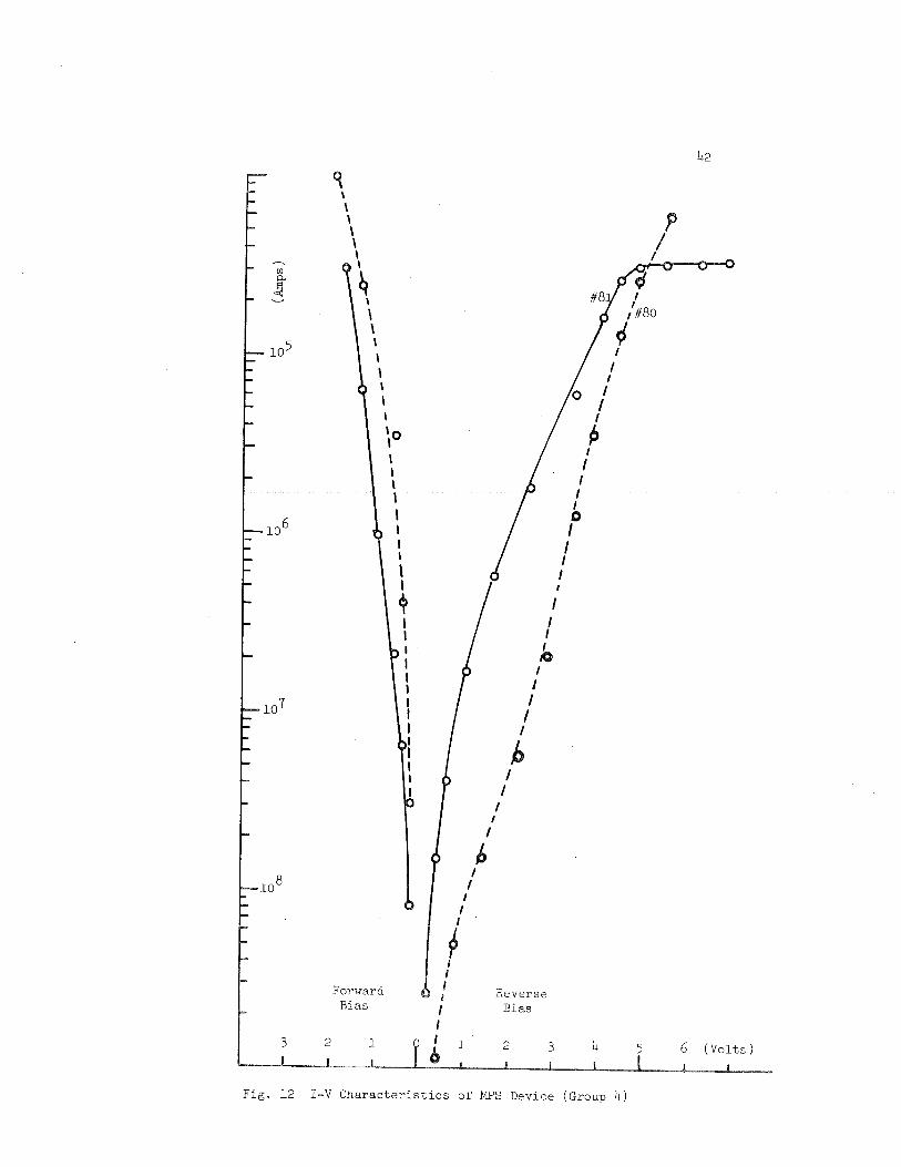
Figure 9 shows t h e I - V c h a r a c t e r i s t i c s o f two W S devf ces
with mechanically po l i shed s i l i c o n wafers . It can be seen t h a t t h e 0
low r e s i s t i v i t y (10 and t h i c k e r f i lms (140 A ) g ives a
symmetric I-V curves i n t h e forward and reverse b i a s e d cond i t i ons -
However, t h e curves of t h e device with h ighe r r e s i s t i v i t y (70 ~ - c m ) 0
and t h i n n e r f i lm (80 A ) show an asymmetric c h a r a c t e r i s t i c s , The 51;)p6'
of t h e I - V curves i n r eve r se b i a s g radua l ly decreases , which i n d i c a t e s
t h e f i e l d begins p e n e t r a t i n g i n t o t h e semiconductor,
Fig. 9 I-V Characteristics of MPS Devices ( ~ r o u ~ 1)
N-type S i , 30R-cm Cp4 etched 60 sec .
0---0 70Q-cm N-type S i Cp4 etched 120,sec. Polymer = 100 A
Fig. 10 I-V Charac te r i s t i c s of MPS Devices (Group 2 )

Fig. 11 I-V Characteristics of MPS Devices ( ~ r o u ~ 3)

The I - V curves of two devices wi th chemically t r e a t e d ( e t ched with
cp4) wafers were showed i n f i g u r e 10, The I-V curves a r e asymmetric and a
s a t u r a t i o n was observed f o r t h e device with wafer of h igher r e s i s t i v i t y
( 70~-cm) and longe r e t ch ing (120 s e c ) , Figure 11 shows I - V curves of two
adjacent devices (1 mm a p a r t ) made on t h e same wafer , The gene ra l shapes
of t h e I - V p l o t s a r e a l i k e , however, t h e magnitude o f cu r r en t s v a r i e s one
t o two o r d e r s .
The I - V curves of another p a i r of devices , made on t h e same
wafer a r e shown i n Figure 12 , The magnitude o f cu r r en t s of t h e two devices
were d i f f e r e n t , One shows t h e s a t u r a t i o n and t h e o t h e r does n o t ,
From t h e s e d a t a s e v e r a l conclusions can be drawn:
1, I n forward b i a s condi t ion : t h e I-V c h a r a c t e r i s t i c o f t h e
MPS devices a r e always s i m i l a r . They a r e independent o f t h e su r f ace
t rea tment and t h e r e s i s t i v i t y o f t h e s i l i c o n wafers being used, Further-
more, t h e i n 1 vs v " ~ always y i e l d s s t r a i g h t l i n e s . It i s be l i eved t h a t
t h e conduction mechanisms governing t h e MPM devices a l s o govern t h e MPS
devices i n t h e forward b i a s cond i t i on ,
2 , I n t h e reverse b i a s cond i t i on : The I - V curves vary from
sample t o sample. The curva tures a r e always i n t h e d i r e c t i o n o f fnc reas ing
dynamic r e s i s t a n c e , It i s extremely s e n s i t i v e t o su r f ace t rea tment of
t h e s i l i c o n wafers ,
3. The formation of dep le t ion l a y e r s and inve r s ion l a y e r s i n
t h e semiconductor su r f ace cause a field-penetratlon-llmlted eonductlon
process* This i s discussed i n d e t a i l i n t h e next s e c t i o n -

4 . There i s more t h a n an 0.06 ev d i f f e r ence of work func t ion
between A 1 and S i ( t h e work func t ion of Al i s 4 . 1 ev and N-type (lo&-cm)
S i i s 3 .8 e v ) . I f t h e dominant mechanism i s Schottky emission t h i s should
y i e l d s e v e r a l o rde r s o f magnitude of cu r r en t d i f f e r ence when changing
t h e p o l a r i t y o f b i a s vol tage on t h e MPS device. However, every device made,
t h e r eve r se b i a s and forward b i a s cu r r en t s show l e s s t h a n one o r d e r o f
magnitude of d i f f e r e n c e , e s p e c i a l l y be fo re t h e inve r s ion l a y e r t a k e s p lace .
This i s an evidence of a dominant Poole-Frenkel e f f e c t .
5 . The cu r ren t s a t u r a t i o n i n r eve r se b i a s vo l t age d i r e c t i o n can
only be seen i n devices made on chemically pol i shed and h ighe r r e s i s t i v i t y
s i l i c o n wafers . However, t h i s i s a necessary but apparent ly no t s u f f i c i e n t
condi t ion .
6 , F i e l d p e n e t r a t i o n i n t o t h e semiconductor can be observed
more e a s i l y i n devices having t h i n n e r polymer f i lms . For devices having
Chicker f i l m s , t h i s p e n e t r a t i o n may poss ib ly be observed at h ighe r vol tage
o r cu r r en t l e v e l s .
C. - An Explanation -- of I - V C h a r a c t e r i s t i c o f MPS Devices Reverse
Bias Condition - Sample #81 w a s s e l e c t e d f o r s tudying t h e I - V c h a r a c t e r i s t i c s
of MPS device i n reverse-bias condi t ion . The vol tage drops across
t h e semiconductor and t h e t o t a l b-ias vo l tage a r e s epa ra t ed from t h e d a t a
of forward and r eve r se cu r r en t a s p l o t t e d i n Figure 1 4 . This s epa ra t ion
can only be j u s t i f i e d i f t h e work func t ion d i f f e r ence between polymer and
semiconductor i s not s i g n i f i c a n t enough t o a f f e c t t h e magnitude of cu r r en t s
when changing t h e p o l a r i t y of b i a s vo l t ages . In o t h e r words, t h e mechanism
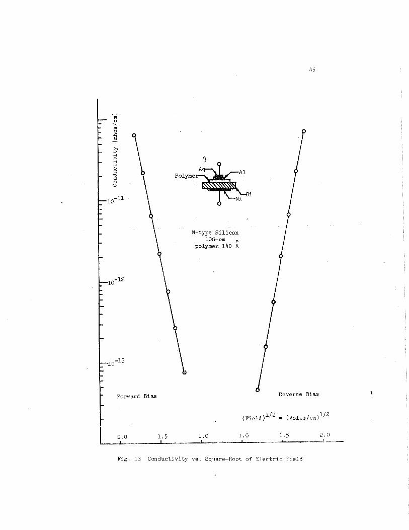
Fig. 13 Conductivity vs. Square-Root of Electric Field

of charge t r a n s p o r t e d through t h e polymer has t o be bulk- l imi ted and
independent of e l e c t r o d e s . Otherwise, t h e ex i s t ence of contac t p o t e n t i a l
may cause a r e c t i f i c a t i o n at t h e polymer-semiconductor i n t e r f a c e . This
r e c t i f i e r could c e r t a i n l y d i s t o r t t h e information f o r s tudying t h e I - V
c h a r a c t e r i s t i c s o f t h e IPS devices i n t h e r eve r se b i a s cond i t i on ,
BY exapining t h e I-V-Character is t ics o f sample #23 i n Figure 1 3
t h e j u s t i f i c a t i o n i s obta ined . Sample #23 was made on a 10Q ern N-type 0
s i l i c o n and t h e polymer i s much t h i c k e r (140 A ) t han most o t h e r MPS 0
devices (-80 A ) .
The conduc t iv i ty versus square-root of f i e l d i n t h e forward
and reverse b i a sed condi t ion i s p l o t t e d i n f i g u r e 1 3 , it can be seen t h a t
t h e p l o t i s two s t r a i g h t l i n e s and n e a r l y symmetric w i th r e spec t t o zero
b i a s . The work func t ions f o r A1 and S i l i c o n (10R cm, N-type) a r e 4 , 1 e v
and 3.8 ev r e spec t ive ly . I f it i s an e l ec t rode l i m i t e d conduction process ,
t h e conductances should vary by s e v e r a l o rde r s o f magnitude when changing
t h e p o l a r i t y of b i a s , This symmetry i s s t rong evidence t h a t t h e conduction
mechanism i s bulk- l imi ted and j u s t i f i e s t h e assumption t h a t no work func t ion
d i f f e r ence i s be ing seen ,
Two "impedances" corresponding t o t h e v ~ l t a g e drop ac ros s t h e
polymer and semiconductor can be a s soc i a t ed wi th t h e MPS devices ,
However, both t h e impedances a r e non-l inear . The impedance of t h e polymer
i s decreasing r a p i d l y wi th b i a s vo l t age , and on t h e o t h e r hand, t h e
impedance of t h e semiconductor w i l l i nc rease wi th i n c r e a s i n g r eve r se b i a s ,
A t low b i a s , e s s e n t i a l l y a l l t h e appl ied vol tage appears ac ros s t h e
polymer, When t h e app l i ed vo l t age i n c r e a s e s , t h e drop ac ros s t h e semi-

conductor begins t o appear , s ince t h e r eve r se b i a s e d semiconductor w i l l
beg ip t o form a dep le t ion reg ion . A t some t r a n s i t i o n vo l t age , t h e impedance
of t h e semiconductor i nc reases t o a value equa l t o t h a t o f polymer, When
t h i s occurs , t h e app l i ed vol tage i s shared equa l ly between t h e polymer and
semiconductor. T h e r e a f t e r , more of t h e vol tage i n excess of t h i s t r a n s i t i o n
w i l l f a l l across t h e semiconductor. The remaining f r a c t i o n across t h e
polymer i s j u s t s u f f i c i e n t t o i n su re cu r r en t c o n t i n u i t y throughout t h e
system.
For MPS devices of t h i c k e r polymer t h e t r a n s i t i o n vol tage i s
expected t o be much h ighe r t han t h e t h i n n e r one, Sample #32 shows t h e
symmetric I -V curves w i t h i n t h e b i a s vol tage range o f i n t e r e s t (,i V o l t s )
and t h e t h i n n e r ones a l r eady show t h e onset of asymmetric c h a r a c t e r i s t i c s .
Bearing t h e s e i n mind, we can cons t ruc t a s e t o f f i g u r e s showing t h e
cur ren t -vol tage r e l a t i o n i n t h e semiconductor. The vo l t age drop i n t h e
polymer and t h e vol tage drop across t h e semiconductor a r e p l o t t e d versus
t h e t o t a l app l i ed vol tage i n Figure 15 and 16 . With t h e s e curves i n
hand, p lus t h e curve o f capaci tance versus b i a s voleage, a f u r t h e r ana lys i s
of t h e I - V c h a r a c t e r i s t i c s o f MPS devices i n t h e r eve r se b i a s condi t ion
can be c a r r i e d ou t .
Wilmsen s t a t e d t h a t t h e cu r r en t through a MPS device i n r eve r se
b i a s should s a t u r a t e when t h e dep le t ion l a y e r i n t h e semiconductor su r f ace
begins t o form. This means cur ren t s a t u r a t i o n happens a t o r before t h e
complete formation of t h e dep le t ion l a y e r , By r e f e r i n g t o f i g u r e l l a n d I?!.
we s e e it i s no t t r u e i n our case , s i n c e t h e cu r r en t satu-rated a t a b i a s
of about 4.8 v o l t s and t h e dep le t ion l a y e r was completely formed around
1 . 2 v o l t s .
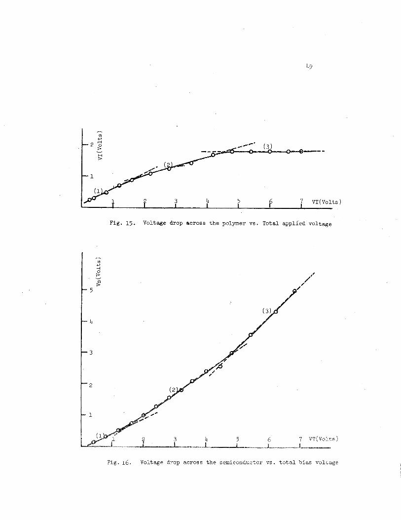
Fig. 15. Voltage drop across t h e polymer vs. To ta l appl ied vol tage
Fig . 16 . Voltage drop across t h e semiconductor vs . t o t a l b ias voltage

Fig. 17 Capacitance versus Voltage

Other mechanisms have t o be adopted i n o rde r t o exp la in t h e
observed phenomena. As has been mentioned t h e t o t a l app l i ed vol tage o r
vo l tage drop ac ros s t h e MPS devices can be separa ted a s vol tage drops
across t h e polymer and/or t h e semiconductor, By c a r e f u l l y s tudying
f i g u r e 1 4 , it can be seen t h a t t h e vol tage drop across t h e semiconductor
may be d iv ided i n t o t h r e e reg ions i f t h r e e approximation l i n e s a r e drawn,
by using t h e same piece-wise l i n e a r technique , Three d i s t i ngu i shab le
reg ions o f d i f f e r e n t I - V c h a r a c t e r i s t i c s can a l s o be obtained i n Figure l k b ,
The r e l a t i o n s h i p s between a reg ion of one curve t o t h e corresponding
reg ion i n ano the r curve w i l l be s t a t e d c l e a r l y l a t e r on,
A s f i g u r e 16 shows, i n reg ion ( 1 ) t h e t o t a l b i a s vo l t age
begins t o drop ac ros s t h e semiconductor, The formation of a dep le t ion
l a y e r i n t h e semiconductor causes t h e vo l t age drop, However, t h e
vo l t age drop i n t h e polymer ( a s shown i n f i g u r e 1 5 ) i s l a r g e a s compared
wi th t h a t ac ros s t h e semiconductor, t h e r e f o r e , t h e cu r r en t i s dominated
by t h e f i e l d ac ros s t h e polymer. The cu r ren t i nc reases sha rp ly wi th
b i a s vo l t age a s shown i n f i g u r e 14b and t h e i n j e c t e d e l e c t r o n s from
t h e polymer t o t h e dep le t ion reg ion w i l l be quick ly swept t o t h e semi-
conductor e l e c t rode through t h e dep le t ion l a y e r ,
I n reg ion (21, t h e vol tage drop across t h e semiconductor i s
comparable w i th t h e vol tage drop across t h e polymer, Due t o t h e h ighe r
vol tage drop an inve r s ion l a y e r apparent ly has begun t o form at t h e
semiconductor su r f ace . This i s s u b s t a n t i a t e d by t h e capaci tance vs b i a s
vol tage curve i n f i g u r e 13 t h e formation of invers ion la,yer causing
t h e capaci tance t o approach a minimum va lue , Actua l ly , t hen , t h e r e i s

a f ie ld- induced p-n junc t ion a t t h e semiconductor su r f ace , The vo l t age
ac ros s t h e polymer i s s t i l l i n c r e a s i n g when t h e b i a s vol tage i n c r e a s e s .
The r a t e o f i n c r e a s e i s s lower, however, a s can be seen i n f i g u r e 15 where
t h e s lope o f t h e curve g radua l ly decreases . The r e s u l t i s s t i l l a polymer
f i e l d dependent I - V curve, bu t t h e s lope i s gradual ly decreasing toward
zero .
S ince t h e r e i s a f ie ld- induced p-n junc t ion a t t h e s e m i c o n d ~ c t ~ o r
s u r f a c e , t h e i n j e c t e d e l e c t r o n s from t h e polymer may be combined w i t h t h e
i o n i c ho le s i n t h e inve r s ion l a y e r , The inve r s ion l a y e r i s not y e t s t r o n g l y
i n v e r t e d , t h e r e f o r e , +he recombination r a t e i s not high and it can be
s a i d t h a t t h e mean f r e e pa th o f t h e i n j e c t e d e l e c t r o n s i n t h i s l a y e r i s
longer t han t h e width of t h e inve r s ion l a y e r . I n j e c t e d e l e c t r o n s may
recombine wi th ho le s i n t h i s reg ion , b u t a l a r g e number w i l l pass through
t o t h e n e u t r a l N region.
I n reg ion ( 3 ) , t h e vol tage drop across t h e semiconductor i s
con t inua l ly i nc reas ing , i t s inc reas ing r a t e i s l i n e a r l y p ropor t iona l t o
t h e inc rease of b i a s vol tage a s can be seen i n Figure 16. A t t h i s reg ion ,
t h e inve r s ion l a y e r i s s t r o n g l y i n v e r t e d , and t h e charge i n t h i s l a y e r i s
tremendously increased . The r e s u l t i s t h a t t h e cu r r en t pass ing through
t h e MPS device i s completely l i m i t e d by t h e recombination r a t e i n t h e
inve r s ion l a y e r . Since d-c cu r r en t flqw has t o be maintained i n t h e
MPS system, ho le s from t h e dep le t ion reg ion have t o be suppl ied t o t h e
inve r s ion l a y e r and an equal number of e l e c t r o n s i n t h e dep le t ion l a y e r
a l s o have t o move t o t h e n e u t r a l N-type reg ion , Thus, t h e cu r r en t i s
equa l ly w e l l l i m i t e d by t h e recombination-generation processes t h a t t ake
p lace i n t h e f ie ld- induced Junc t ion ,

Recal l t h a t i n an ord inary r eve r se b iased p-n junc t ion t h e r e
a r e two b a s i c cur ren t components ; t h e genera t ion cu r r en t i n t h e dep le t ion
reg ion of t h e junc t ion and t h e d i f f u s i o n cu r ren t caused by el.ectron-hole
p a i r genera t ion i n t h e n e u t r a l P and N reg ions . I n t h e n e u t r a l reg ion
t h e r e i s no s i g n i f i c a n t e l e c t r i c f i e l d p re sen t and t h e minori ty c a r r i e r s
move only by d i f fus ion .
For t h e d i f fus ion-cur ren t component, only those minor i ty
c a r r i e r s which a r e generated w i t h i n a d i f fus fon l eng th o f t h e edge of
t h e dep le t ion region w i l l c o n t r i b u t e t h e d i f f u s i o n c u r r e n t , because
only t h o s e have a chance t o reach t h e edge of t h e dep le t ion r eg ion ,
Thus one would expect t h e d i f f u s i o n cu r ren t t o be given a s
I d i f f = q[ne t gene ra t ion r a t e p e r un i t volume i n t h e
n e u t r a l r eg ion ] X [d i f fus ion l e n g t h ] , A j
where Aj = junc t ion c ros s - sec t iona l a r e a .
Assuming no i l l umina t ion and p < e p n o o r n < c n w h e r e p , n a r e n P PO ' n p
concent ra t ion o f holes o r e l e c t r o n i n an n-type o r p-type semiconductor,
and pno, n a r e values o f p n i n equi l ibr ium, t h e d i f f u s i o n cu r ren t PO n ' P
i n t h e N-region can be given a s
where T i s l i f e t i m e of ho les i n an N-type reg ion , L i s d i f f u s i o n l e n g t h , P P
A s i m i l a r expression can be given f o r I d i f f
i n p reg ion ,

I n a reverse-biased dep le t ion reg ion , t h e r a t e of genera t ion
of e lec t ron-hole p a i r s can be obta ined a s 3 0
where T i s def ined as t h e e f f e c t i v e l i f e t i m e wi th in a reverse-biased 0
dep le t ion reg ion and i s given by
( E -E )/kT + a e t i ( Ei-Et ) /kT 1: = ' n P
where o ,a = capture c ross -sec t ion a r e a o f e l e c t r o n and t h e ho le r e s p e c t i v e l y
Et = energy l e v e l of recombination
E. = an e l e c t r o n energy a t t h e i n t r i n s i c Fermi Level 1
Vth = thermal v e l o c i t y o f c a r r i e r s
Nt = concent ra t ion o f bulk recombination-generation cen te r s p e r un i t volume,
One e l e c t ron-hole p a i r genera ted provides one e l e c t r o n i c
charge t o t h e e x t e r n a l c i r c u i t , Thus, t h e magnitude of cu r r en t due t o
genera t ion wi th in t h e dep le t ion reg ion w i l l be given by
WAJ
The important po in t i s t h a t t h e generat ion-current component i s dependent
on t h e magnitude of t h e app l i ed r eve r se b i a s , A t h ighe r b i a s W i s Larger ,
more cen te r s a r e included wi th in t h e deple t ion reg ion , and t h e genera t ion
cu r r en t i nc reases i n p ropor t ion t o W.
I n a reverse-biased P-N junc t ion (assume a s t e p j u n c t i o n ) ,
t h e t o t a l dep le t ion region width W a s a func t ion of t h e t o t a l e l e c t r o -
s t a t i c , p o t e n t i a l v a r i a t i o n from one s i d e of t h e junc t ion t o t h e o t h e r
(e , ) , i s
where (PT i s r e f e r r e d t o a s t h e b u i l t - i n vol tage o f a p-n junc t ion and
N and N a r e concent ra t ions of acceptor and donor i m p u r i t i e s , a d
A p a r t i c u l a r case o f s t e p junc t ions which i s o f t e n encountered
i n p r a c t i c e i s a s t e p junc t ion where one s i d e i s more heav i ly doped
than t h e o t h e r , f o r example, N << Nd This r e s u l t s i n a s impler form a
f o r t h e dep le t ion l a y e r width,
I n ou r non-equilibrium f ield- induced p-n junc t ion t h e above
equat ion s t i l l ho lds , however, t h e I$ term has t o be rep laced by 7
(Pb + +s + Va, where I$b, I$s and V a r e def ined i n Figure 18, a

Invers ion Laver
Figure 18
Because of t h e r e l a t i v e l y l a r g e conductance of t h e invers ion
l a y e r , t h e e n t i r e b i a s , Va, appears across t h e dep le t ion region
between t h e invers ion l a y e r and t h e bulk. Thus, V i s a c t u a l l y t h e V a s
a s defined i n Figure 14b.
Therefore, t h e generat ion current can be expressed as
it w i l l i nc rease with square root vol tage drop across semiconductor.
The increase i s v e r y ' s m a l l , any increase I n polymer vol tage i s
exceedingly smal l .

Current i n reg ion ( 3 ) of t h e MPS device i s l i m i t e d by t h e
d i f f u s i o n and genera t ion c u r r e n t s i n t h e f ie ld- induced p-n junc t ion
The d i f f u s i o n cu r ren t component i s independent of b i a s vo l t age , however,
and t h e l i m i t i n g term i s a c t u a l l y t h e electron-hole p a i r generat ion i n
t h e dep le t ion region.
An important po in t i s t h a t t h e genera t ion cu r r en t i s dependent.
upon t h e width of dep le t ion l a y e r , For h igher r e s i s t i v i t y semiconduct,ors
t h e doping dens i ty i s lower, t hus t h e width i s l a r g e r and a h igher ,
s a t u r a t i o n cu r r en t l e v e l should be observed f o r t h e MPS devices" On t h e
o t h e r hand, f o r MPS devices made on lower r e s i s t i v i t y semieonduetors it
i s expected t h e cu r r en t would be s a t u r a t e d at lower l e v e l , This i s
e x a c t l y what our experimental d a t a show. Referr ing t o f i gu res 11 and
1 2 , it can be seen t h e device (#81) of lower r e s i s t . i v i t y ( 70Q em)
s a t u r a t e d a t a l e v e l lower than t h e h igher r e s i s t i v i t y devices (#54 and
55 , 113Q cm)
Besides t h e genera t ion and d i f fus ion c u r r e n t s , leakage and
avalanche e f f e c t s may e x i s t i n t h e MPS device system. When one o r both
of them e x i s t s t h e r eve r se cu r r en t may never become s a t u r a t e d , o r may
s a t u r a t e a t h ighe r l e v e l ,
A c ross -sec t ion a r e a p i c t u r e f o r a MPS device of reverse b i a s
i s shown below
Polymer Depletion Layer
Invers ion Layer Area Defined a s A 3
Top Elect rode
Neut ra l N --J* \___I
Begion /--.-_- /
Figure19 Cross Sec t ion of an MPS Device
The surface s t a t e s a t t h e i n t e r f a c e of t h e polymer and semicon-
ductor may a c t a s t r a p s o r recombination cen te r s . Thus, it may cont r ibute
a surface component of current by r e l eas ing c a r r i e r s from t r a p s , This can
be expressed as
where A i s t h e a rea defined i n Figure 1 9 , and s
U i s t h e c a r r i e r generat ion r a t e p e r u n i t sur face a r e a s
and i s a funct ion of su r face s t a t e dens i ty , t h e i r capture cross sec t ion
and thermal v e l o c i t y of c a r r i e r s .
Those sur face s t a t e s may serve a s a by-pas's between t h e invers ion
l a y e r and t h e N-type n e u t r a l region. Thus t h e MPS device may not s a t u r a t e
a s it should, This a l s o expla ins why t h e current through MPS devices
i n reverse-biased condi t ion i s extremely s e n s i t i v e t o sur face prepara t ion .
Within t h e field-induced junct ion, de fec t s may be present . Those
defec ts w i l l lower t h e breakdown voltage of t h e f ield-induced junct ion , thus
a l a r g e excess reverse current w i l l be observed even a t r e l a t i v e l y low
reverse b ia ses . Current s a t u r a t i o n can never be seen i n t h i s case. Defects
may be introduced by mechanically lapping and po l i sh ing t h e s i l i c o n wafers.
Strong chemical e tching may e a t away t h e de fec t s and y i e l d b e t t e r r e s u l t s ,
This serves t o expla in why adequate chemical e t ch ing i s p re fe r red f o r
observat ion of current s a t u r a t i o n of MPS devices,

CHAPTER V
CONCLUSION
The e l e c t r i c a l conduct iv i ty of t h i n polymer f i lms produced by
e l e c t r o n bombardment of D.C. 704 d i f f u s i o n pump o i l does not appear t o
be explained completely by any one o f t h e simple mechanisms t h e o r e t i c a l l y
app l i cab le t o t h i n d i e l e c t r i c f i lms . The observed behavior can be
descr ibed s a t i s f a c t o r y by Poole-Frenkel emission at room temperature, Even
t h e n t h e d e s c r i p t i o n i s no t completely adequate , because t h e I - V C h a r a c t e r i s t i c
may have two o r more asymptotes. A combination of Poole-Frenkel and
Schottky emissions may have t o be assumed t o j u s t i f y t h e s lope changes.
For example two types of de fec t s with Poole-Frenkel behavior may adequately
c h a r a c t e r i z e charge t r a n s p o r t through t h e polymer.
The l i m i t i n g e lec t ron-hole p a i r genera t ion i n t h e dep le t ion
reg ion af'ter t h e MPS device has been s t r o n g l y i n v e r t e d exp la ins t h e
cu r r en t s a t u r a t i o n of MPS devices i n r eve r se b i a s condi t ion . This
s a t u r a t i o n may not 'be observed because su r f ace leakage cu r ren t in t roduced
by su r f ace s t a t e s i n t h e polymer-semiconductor i n t e r f a c e , The de fec t s
w i th in t h e f ie ld- induced P-N junc t ion may c o n t r i b u t e a cur ren t component.,
t h u s s a t u r a t i o n may a l s o not be observed, These a l s o exp la in why t h e MPS
device i s extremely s e n s i t i v e t o sur face p repa ra t ion s i l i c o n of h ighe r
r e s i s t i v i t y and s t r o n g chemical e t ch ing seems t o y i e l d b e s t r e s u l t s ,
The purpose of t h i s research p r o j e c t i s t o b u i l d a vol tage /
cu r r en t d i g i t a l t r ansduce r by in te rconnect ion s e v e r a l of t h e s e s a t u r a t i n g

W S devices . Experimental r e s u l t s showed t h i s i s very poss ib l e , For
obta in ing s t a b l e and reproducable r e s u l t s , t h e s i l i c o n may have t o be
p ro t ec t ed by an oxide l a y e r . S i l i c o n dioxide would be grown on t h e
s i l i c o n su r f ace f i r s t , aed then window opened by using photo r e s i s t
technique. The polymer would then be depos i ted i n t h e windows t o make
t h e MPS devices . The KPS devices could then se rve a s t h e "stepping
s tones" t o b u i l d v o l t age /cur ren t d i g i t a l t r ansduce r s and a l s o provides
a way of s tudy t h e semiconductor su r f ace p r o p e r t i e s ,

BIBLIOGRAPHY
1 , G . Glocker and S.C. Lind, The Electrochemistry of Gases and Other D i - e l e c t r i c s , J . Wiley and Sons, I n c . , New York, 1939.
2 . J. H i l l i e r , "On I n v e s t i g a t i o n of Specimen Contamination i n Elec t ron -
~ i c r o s c o ~ e ," J. Appl. Phys. , Vol. 1 9 , No. 3 , Mar. , 1948, pp. 226-30.
3. J . H . L. Watson, "Effec t of Elec t ron Bombardment Upon Carbon lack ," J. Appl. Phys. , Vol. 1 8 , No. 2 , Feb., 1947, pp. 153-61.
4. L. Holland and L. Laurenson, "The E l e c t r i c a l P rope r t i e s of S i l i c o n e Films Polymerized by E lec t ron Bombardment," Vacuum, Vol. 1 4 , June, 1964, pp. 325-332.
5 . D. R. Lamb, E l e c t r i c a l Conduction Mechanisms i n Thin I n s u l a t i n g Fi lms, ~ ~ o t t ' i s w ~ o d e , Bal lantyne and Co . , Lt d. , London, 1967.
6. J . Frenkel , "Pre-Breakdown Phenomena i n I n s u l a t o r s and E l e c t r o n i c Semiconductors ," Phys. Rev. , Vol. 54, 1938, pp. 647.
7. L.L. Chang, P . J . S t i l e s , and L. Esaki , "Electron Tunneling Between a Metal and a Semiconductor: C h a r a c t e r i s t i c s of A1-A1 0 -SnTe and - GeTe Junct ions ," J . Appl. Phys . , Vol. 38, 2 3
NO. 11, ~ c t . , 1967, pp. 4440-4445.
8. V. E. Dahlke , "Tunneling i n t o Interface S t a t e s of MOS S t r u c t u r e s ," App. Phys. L e t t e r s , Vol. 1 0 , No. 1 0 , May, 1967, pp. 261- 262.
9. C . W . Wilmsen, "Tunneling Between a Metal and S i l i c o n Separated by a Polymer I n s u l a t o r ," D i s s e r t a t i o n , Univers i ty of Texas, 1967.
10. L.V. G r e g ~ r and L.H. Kaplan, " E l e c t r i c a l Conductivity of Thin Poly- mer Films," Thin S o l i d Fi lms, Vol. 2 , J a n . , 1968, pp. 95-103.
11. E.T. F i tzg ibbons , "Charge Transport Mechanisms i n Thin Polymer Films," Thesis , Univers i ty of Texas, 1967.
12. P.R. Emtage and W. Tantraporn, " ~ c h o t t k ~ Emission Through Thin Insu- l a t i n g Films," Phys. Rev. L e t t e r s , Vol. 8 , No. 7 , Apr. 1, 1962, pp. 267-268.
13. J .T . Wallmark and H . Johnson, F ie ld-Effec t T r a n s i s t o r s , P ren t i ce - H a l l , I n c . , Englewood C l i f f s , New Jersey, 1966.

J . L . Moll, McGraw-Hill, New York, 1964.
R . S t r a t t o n , "Volt-Current C h a r a c t e r i s t i c s f o r Tunneling Through In- s u l a t i n g Fi lms, J . Phys. Chem. S o l i d s , Vol. 23, 1963, pp. 1177-1190.
J. G. Simmons , " P o t e n t i a l B a r r i e r s and Emis sion-Limited Current Flow Between Closely Spaced P a r a l l e l Metal ~ l e c t r o d e s , " J. Appl. Phys. , Vol. 35, No. 8, Aug, 1964, pp. 2472-2481.
J . W . Conley, C.B. Duke, G.D . Mahan, and J.J. Tiemann, "Elec t ron Tun- n e l i n g i n Metal-Semiconductor Ba r r i e r s , " Phys. Rev., Vol. 150 , NO. 2 , Oct. 1966, pp. 466-469.
P.V. Gray, "Tunneling from Metal t o Semiconductors ," Phys. Rev. , Vol. 1 4 0 , NO. 1 A , Oct . , 1965, pp. ~ 1 6 9 - ~ 1 8 6 .
J . G . Simmons, "Generalized Formula f o r t h e E l e c t r i c Tunnel E f f e c t Be- tween S imi l a r Elec t rodes Separated by a Thin I n s u l a t i n g -
~ i l m , " J . Appl. Phys. , Vol. 34 , No. 6 , June, 1963, pp. 1793 -1803.
J . R . Yeargan, "Charge Transport Mechanisms i n Thin S i l i c o n N i t r i d e Films ," D i s s e r t a t i o n , Univers i ty of Texas, 1967.
J. G . Simmons, "Poole-Frenkel E f fec t and Schottky E f f e c t i n Metal- Insulator-Metal systems ," Phys. Rev. , Vol. 155, No. 3 , Ibr. , 1967, pp. 657-660.
J. G , Simmons , "Trans i t ion from Electrode-Limited t o Bulk-Limited Con- duct ion Processes i n Metal-Insulator-Metal Systems ," Phys. Rev Vol. 166, No. 3, Feb. , 1968, pp. 912-920. .,
A. Many, Y . Golds te in , and N .B. Grover, Semiconductor Surf a c e s , John Wiley and Sons, I n c . , New York, 1965.
R. M. Warner, I n t e g r a t e d C i r c u i t s Design P r i n c i p l e s and F a b r i c a t i o n , McGraw-Hill Co., New York, 1965.
D.R. F rankl , E l e c t r i c a l P rope r t i e s of Semiconductor Su r faces , Pergamon P r e s s , Ltd. , Oxford, 1967.
N.F. Mott and R.W. Gurney, E l e c t r o n i c Processes i n Ion ic C r y s t a l s , Dover Pub l i ca t ions , Inc . , New York, 1964.
F. J. Biondi , T rans i s to r Technology, V Q ~ . 111, B e l l Lab S e r i e s , Nostrand Co. , Inc . , Pr ince ton , New J e r s e y , 1958,
A.E. Ennes, "Sources of Electron-Inducted Contamination, i n K ine t i c Vacuum Systems," , Vol. 5 , No, 1, 1954, pp. 27-31.
9 R.W. Christy, "Formation of Thin Polymer Films by Electron Bombardment," J. Appl. Phys., Vol. 31, No. 9, Sept., 1960, pp. 1680-3.
30. R.N. Hall, "Electron- ole Recombination in Germanium," Phys. Rev., Vol, 87, 1952, p. 387.
31. W. Shockley and W.T. Read, "Statistics of the Recombination of Holes and Electrons ,'I Phys . Rev. , Vol. 87, 1952, pp. 835-844.