electronic properties of graphene from tight-binding...
TRANSCRIPT

9HSTFMG*afibeg+
ISBN 978-952-60-5814-6 ISBN 978-952-60-5815-3 (pdf) ISSN-L 1799-4934 ISSN 1799-4934 ISSN 1799-4942 (pdf) Aalto University School of Science Department of Applied Physics www.aalto.fi
BUSINESS + ECONOMY ART + DESIGN + ARCHITECTURE SCIENCE + TECHNOLOGY CROSSOVER DOCTORAL DISSERTATIONS
Aalto-D
D 12
2/2
014
Andreas U
ppstu E
lectronic properties of graphene from tight-binding sim
ulations A
alto U
nive
rsity
Department of Applied Physics
Electronic properties of graphene from tight-binding simulations
Andreas Uppstu
DOCTORAL DISSERTATIONS
Aalto University publication series DOCTORAL DISSERTATIONS 122/2014
Electronic properties of graphene from tight-binding simulations
Andreas Uppstu
A doctoral dissertation completed for the degree of Doctor of Science (Technology) to be defended, with the permission of the Aalto University School of Science, at a public examination held at lecture hall M1 (Otakaari 1, Espoo) of the school on 12 September 2014 at 13.
Aalto University School of Science Department of Applied Physics
Supervising professor Aalto Distinguished Professor Risto Nieminen Thesis advisor Adjunct Professor Ari Harju Preliminary examiners Doctor Jani Kotakoski, University of Vienna, Austria Professor Igor Zozoulenko, Linköping University, Sweden Opponent Professor Oleg Yazyev, École Polytechnique Fédérale de Lausanne, Switzerland
Aalto University publication series DOCTORAL DISSERTATIONS 122/2014 © Andreas Uppstu ISBN 978-952-60-5814-6 ISBN 978-952-60-5815-3 (pdf) ISSN-L 1799-4934 ISSN 1799-4934 (printed) ISSN 1799-4942 (pdf) http://urn.fi/URN:ISBN:978-952-60-5815-3 Unigrafia Oy Helsinki 2014 Finland
Abstract Aalto University, P.O. Box 11000, FI-00076 Aalto www.aalto.fi
Author Andreas Uppstu Name of the doctoral dissertation Electronic properties of graphene from tight-binding simulations Publisher School of Science Unit Department of Applied Physics
Series Aalto University publication series DOCTORAL DISSERTATIONS 122/2014
Field of research Theoretical and computational Physics
Manuscript submitted 12 May 2014 Date of the defence 12 September 2014
Permission to publish granted (date) 18 June 2014 Language English
Monograph Article dissertation (summary + original articles)
Abstract Graphene is an effectively two-dimensional semimetallic material consisting of a sheet of
carbon atoms arranged in a hexagonal lattice. Due to its high electron mobility and special electronic properties, it is considered to be a promising candidate for various future electronic applications. Freestanding graphene was discovered as late as in 2004, but since then it has become the focus of numerous studies, sparking not only scientific but also significant commercial interest.
Realizing the potential of the material requires both theoretical, numerical, and experimental
studies. An important computational model for studying the electronic properties of graphene is the so-called tight-binding (TB) model. In the TB model, the charge carriers of a material are described using effective parameters, which can be either derived from more complex models or fitted to experimental or computational results.
In this Thesis, the TB model was used to study both the local density of states (LDOS) of
graphene as well as electronic transport in graphene. Simulating the LDOS of graphene is important, since it may be more or less directly measured using scanning tunneling microscopy (STM), and is thus extremely helpful for characterizing the properties of nanometer-sized graphene samples. The results presented in this Thesis, which show good agreement between simulations and STM measurements, help to determine the electronic structure of graphene quantum dots on various substrates.
Simulations of electronic transport aid in making graphene useful for semiconductor
applications. Graphene may be turned semiconducting by various means, such as by cutting it into ribbons or by adding disorder. In this Thesis, it was showed how scaling theory can be utilized to obtain the conductance of a mesoscopically sized disordered graphene device using first-principles-based results and how the localization length of the charge carriers can be obtained effectively using the so-called Kubo-Greenwood method. The results aid in interpreting experimental conductance measurements and in estimating how strong disorder is required to turn graphene into an effective semiconductor.
Keywords graphene, tight-binding, electronic transport, scanning tunneling microscopy
ISBN (printed) 978-952-60-5814-6 ISBN (pdf) 978-952-60-5815-3
ISSN-L 1799-4934 ISSN (printed) 1799-4934 ISSN (pdf) 1799-4942
Location of publisher Helsinki Location of printing Helsinki Year 2014
Pages 170 urn http://urn.fi/URN:ISBN:978-952-60-5815-3


Sammandrag Aalto-universitetet, PB 11000, 00076 Aalto www.aalto.fi
Författare Andreas Uppstu Doktorsavhandlingens titel Grafens elektroniska egenskaper från starkbindningssimuleringar Utgivare Högskolan för teknikvetenskaper Enhet Avdelningen för teknisk fysik
Seriens namn Aalto University publication series DOCTORAL DISSERTATIONS 122/2014
Forskningsområde Teoretisk och numerisk fysik
Inlämningsdatum för manuskript 12.05.2014 Datum för disputation 12.09.2014
Beviljande av publiceringstillstånd (datum) 18.06.2014 Språk Engelska
Monografi Sammanläggningsavhandling (sammandrag plus separata artiklar)
Sammandrag Grafen är ett effektivt tvådimensionellt material som består av kolatomer arrangerade i ett
hexagonalt gitter. Tack vare speciella elektroniska egenskaper, som laddningsbärarnas höga mobilitet, anses grafen vara en lovande kandidat för framtida elektroniska tillämpningar. Fristående grafen upptäktes så sent som 2004, men sedan dess har materialet blivit fokus för otaliga studier. Förutom ett vetenskapligt intresse, har grafen under den senaste tiden också skapat ett betydande kommersiellt intresse.
För att förverkliga materialets potential krävs både teoretiska, numeriska och experimentella
studier. Den så kallade starkbindningsmodellen är en viktig numerisk modell för simulering av grafen. I starkbindningsmodellen beskrivs laddningsbärarna med hjälp av effektiva parametrar, som kan härledas med hjälp av mera komplexa numeriska metoder eller genom att anpassa dem till experimentella resultat.
I denna avhandling används starkbindningsmodellen till att simulera både lokal
tillståndstäthet samt elektronisk transport i grafen. Att simulera lokal tillståndstäthet är viktigt, eftersom den kan mer eller mindre direkt mätas genom sveptunnelmikroskopi. Därmed är metoden extremt användbar för att karakterisera nanometerstora grafenflagor. Resultaten som presenteras i denna avhandling visar att simuleringarna stämmer bra överens med experimentella resultat.
Simuleringar av elektronisk transport kan hjälpa med att få grafen användbart för
halvledarapplikationer. Grafen kan fås till att bli en halvledare med olika metoder, till exempel genom att skära den i strimlor eller lägga till oordning i det annars perfekta gittret. I denna avhandling visas hur man kan använda ab initio -baserade metoder för att beräkna grafens konduktans och hur den så kallade Kubo-Greenwood-metoden kan användas till att beräkna laddningsbärarnas lokaliseringslängd. Dessa resultat hjälper att tolka experimentella mätresultat och att estimera hur stark oordning krävs för att ändra grafen till en effektiv halvledare.
Nyckelord grafen, starkbindning, elektronisk transport, sveptunnelmikroskopi
ISBN (tryckt) 978-952-60-5814-6 ISBN (pdf) 978-952-60-5815-3
ISSN-L 1799-4934 ISSN (tryckt) 1799-4934 ISSN (pdf) 1799-4942
Utgivningsort Helsingfors Tryckort Helsingfors År 2014
Sidantal 170 urn http://urn.fi/URN:ISBN:978-952-60-5815-3


Preface
This work has been performed in the Quantum Many-Body Physics group,
led by my instructor Dr. Ari Harju. I want to thank Ari for helpful dis-
cussions and all of his support, as well as all of the the current and past
members of the group for creating a nice working environment. I want to
thank my supervisor, Prof. Risto Nieminen, for giving me the opportunity
to work at the Academy of Finland Center of Excellence in Computational
Nanoscience. I also want to thank all of my co-authors, many of whom
work in collaborating groups led by Professors Pertti Hakonen, Peter Lil-
jeroth, Martti Puska, Ingmar Swart and Daniel Vanmaekelbergh. I want
to specifically thank Prof. Peter Liljeroth for giving me the opportunity to
continue working at the university for a while, and my co-worker Mikko
Ervasti for making coffee almost every working day.
Espoo, August 13, 2014,
Andreas Uppstu
1

Preface
2
Contents
Preface 1
Contents 3
List of Publications 5
Author’s Contribution 7
1. Introduction 11
2. Computational methods 15
2.1 The tight-binding model . . . . . . . . . . . . . . . . . . . . . 15
2.2 The Hubbard model . . . . . . . . . . . . . . . . . . . . . . . . 17
2.3 Density functional theory . . . . . . . . . . . . . . . . . . . . 18
2.4 Methods for computing the local density of states . . . . . . 19
2.5 Methods for transport calculations . . . . . . . . . . . . . . . 20
2.5.1 The Landauer-Büttiker formalism . . . . . . . . . . . 20
2.5.2 The Kubo-Greenwood method . . . . . . . . . . . . . . 21
3. The electronic structure of graphene 23
3.1 Band structure . . . . . . . . . . . . . . . . . . . . . . . . . . . 23
3.2 Comparisons between simulations and scanning tunneling
microscopy results . . . . . . . . . . . . . . . . . . . . . . . . . 27
4. Electronic transport in graphene 31
4.1 Ballistic transport and Fabry-Pérot resonances . . . . . . . . 31
4.2 Transport in disordered graphene . . . . . . . . . . . . . . . . 33
4.3 Effective scattering cross-section formalism . . . . . . . . . . 35
4.4 Electronic transport in a magnetic field . . . . . . . . . . . . 40
4.5 Spin-dependent transport . . . . . . . . . . . . . . . . . . . . 41
4.6 Phonon-assisted transport . . . . . . . . . . . . . . . . . . . . 43
5. Summary 47
Bibliography 51
Publications 55
3

Contents
4

List of Publications
This thesis consists of an overview and of the following publications which
are referred to in the text by their Roman numerals.
I Y. Hancock, A. Uppstu, K. Saloriutta, A. Harju and M. J. Puska. Gene-
ralized tight-binding transport model for graphene nanoribbon-based
systems. Physical Review B, 81, 245402, 2010.
II J. van der Lit, M. P. Boneschanscher, D. Vanmaekelbergh, M. Ijäs, A.
Uppstu, M. Ervasti, A. Harju, P. Liljeroth and I. Swart. Suppression of
electron-vibron coupling in graphene nanoribbons contacted via a single
atom. Nature Communications, 4, 2023, 2013.
III M. Ijäs, M. Ervasti, A. Uppstu, P. Liljeroth, J. van der Lit, I. Swart,
and A. Harju. Electronic states in finite graphene nanoribbons: Effect
of charging and defects. Physical Review B, 88, 075429, 2013.
IV S. K. Hämäläinen, Z. Sun, M. P. Boneschanscher, A. Uppstu, M. Ijäs,
A. Harju, D. Vanmaekelbergh, and Peter Liljeroth. Quantum-Confined
Electronic States in Atomically Well-Defined Graphene Nanostructures.
Physical Review Letters, 107, 236803, 2011.
V R. Drost, A. Uppstu, F. Schulz, S. K. Hämäläinen, M. Ervasti, A. Harju,
and P. Liljeroth. Electronic States at the Graphene - Hexagonal Boron
Nitride Zigzag Interface. Accepted for publication in Nano Letters, July
2014.
VI Z. Fan, A. Uppstu, T. Siro and A. Harju. Efficient linear-scaling quan-
tum transport calculations on graphics processing units and applica-
tions on electron transport in graphene. Computer Physics Communica-
tions, 185, 28, 2014.
VII M. Oksanen, A. Uppstu, A. Laaksonen, D. J. Cox, M. F. Craciun, S.
Russo, A. Harju and P. Hakonen. Single-mode and multimode Fabry-
Perot resonances in graphene. Physical Review B, 89, 121414(R), 2014.
VIII A. Uppstu, Z. Fan and A. Harju. Obtaining localization properties
effectively using the Kubo-Greenwood formalism. Physical Review B,
89, 075420, 2014.
5
List of Publications
IX A. Uppstu, K. Saloriutta, A. Harju, M. Puska and A.-P. Jauho. Elec-
tronic transport in graphene-based structures: An effective cross-section
approach. Physical Review B, 85, 041401(R), 2012.
X K. Saloriutta, A. Uppstu, A. Harju and M. J. Puska. Ab initio transport
fingerprints for resonant scattering in graphene. Physical Review B, 86,
235417, 2012.
XI A. Uppstu and A. Harju. High-field magnetoresistance revealing scat-
tering mechanisms in graphene. Physical Review B, 86, 201409(R),
2012.
XII Y. Hancock, K. Saloriutta, A. Uppstu, A. Harju and M. J. Puska. Spin-
Dependence in Asymmetric, V-Shaped-Notched Graphene Nanoribbons.
Journal of Low Temperature Physics, 153, 393, 2008.
6

Author’s Contribution
Publication I: “Gene-ralized tight-binding transport model forgraphene nanoribbon-based systems”
The author wrote the first draft of the manuscript and performed the
tight-binding calculations.
Publication II: “Suppression of electron-vibron coupling in graphenenanoribbons contacted via a single atom”
The author participated in interpreting the experimental results and per-
forming the computational simulations by writing the transport code.
Publication III: “Electronic states in finite graphene nanoribbons:Effect of charging and defects”
The author performed the Hubbard mean-field calculations and partici-
pated in discussing and interpreting the results.
Publication IV: “Quantum-Confined Electronic States in AtomicallyWell-Defined Graphene Nanostructures”
The author performed the tight-binding calculations for the large flakes
and participated in interpreting the experimental results.
Publication V: “Electronic States at the Graphene - Hexagonal BoronNitride Zigzag Interface”
The author performed the tight-binding calculations and participated in
discussing and interpreting the experimental results.
7
Author’s Contribution
Publication VI: “Efficient linear-scaling quantum transportcalculations on graphics processing units and applications onelectron transport in graphene”
The author performed the tight-binding calculations and participated in
discussing the results.
Publication VII: “Single-mode and multimode Fabry-Perotresonances in graphene”
The author wrote most of the manuscript (excluding the supplementary
material), performed the computational simulations and participated in
analyzing the experimental data.
Publication VIII: “Obtaining localization properties effectively usingthe Kubo-Greenwood formalism”
The author wrote the first draft of the manuscript, performed most of the
tight-binding simulations and participated in interpreting the results.
Publication IX: “Electronic transport in graphene-based structures:An effective cross-section approach”
The author performed all tight-binding calculations and wrote the first
draft of the manuscript.
Publication X: “Ab initio transport fingerprints for resonantscattering in graphene”
The author came up with the main idea for the study, performed a part of
the tight-binding calculations and participated in discussing the results.
Publication XI: “High-field magnetoresistance revealing scatteringmechanisms in graphene”
The author wrote the manuscript and performed all calculations.
8

Author’s Contribution
Publication XII: “Spin-Dependence in Asymmetric,V-Shaped-Notched Graphene Nanoribbons”
The author came up with the idea for the manuscript, performed all tight-
binding calculations and wrote the first draft of the manuscript.
9

Author’s Contribution
10

1. Introduction
Graphene is an effectively two-dimensional material formed by a sheet of
carbon atoms arranged into a hexagonal lattice. As it exhibits very spe-
cial electronic and mechanical properties, an enormous scientific and com-
mercial interest has grown around the material during the recent years.
Freestanding graphene was discovered as recently as in 2004 by Andre
Geim and Konstantin Novoselov [1], which earned them the Nobel Prize
in Physics 2010. However, prior to this, graphene had already been syn-
thesized on top of various substrates [2, 3]. As it is closely related to
graphite, and due to its peculiar electronic properties, it had also been
studied theoretically and computationally already since 1947 [4].
In the graphene lattice, the four valence electrons of carbon are ar-
ranged into σ and π bonds [5]. The energy bands that correspond to the π
bonds intersect conically at the charge neutrality point, which gives rise
to unique electronic features, such as the half-integer quantum Hall ef-
fect [6, 7]. The conical intersections occur at the corners of the hexagonal
Brillouin zone, which leads to the formation of two inequivalent valleys
in the electronic band structure. The two fact that a hexagonal lattice
consists of two sublattices adds another degree of freedom for the charge
carriers. Such a system with two degrees of freedom and a linear disper-
sion relation can be modeled by a Dirac equation for massless fermions,
albeit with an effective velocity of light that equals the Fermi velocity of
graphene, i.e. ∼ 106 m/s [5]. The relativistic nature of the charge carriers
leads to phenomena such as Klein tunneling and Zitterbewegung [8, 9].
Graphene can be seen as the basic building block of a variety of materi-
als with different dimensionalities, such as quasi-one-dimensional nano-
ribbons or nanotubes, zero-dimensional fullerenes or three-dimensional
graphite [9]. Depending on the edge type, there are two basic kinds
of graphene nanoribbons (GNRs), called armchair-edged GNRs (AGNRs)
11
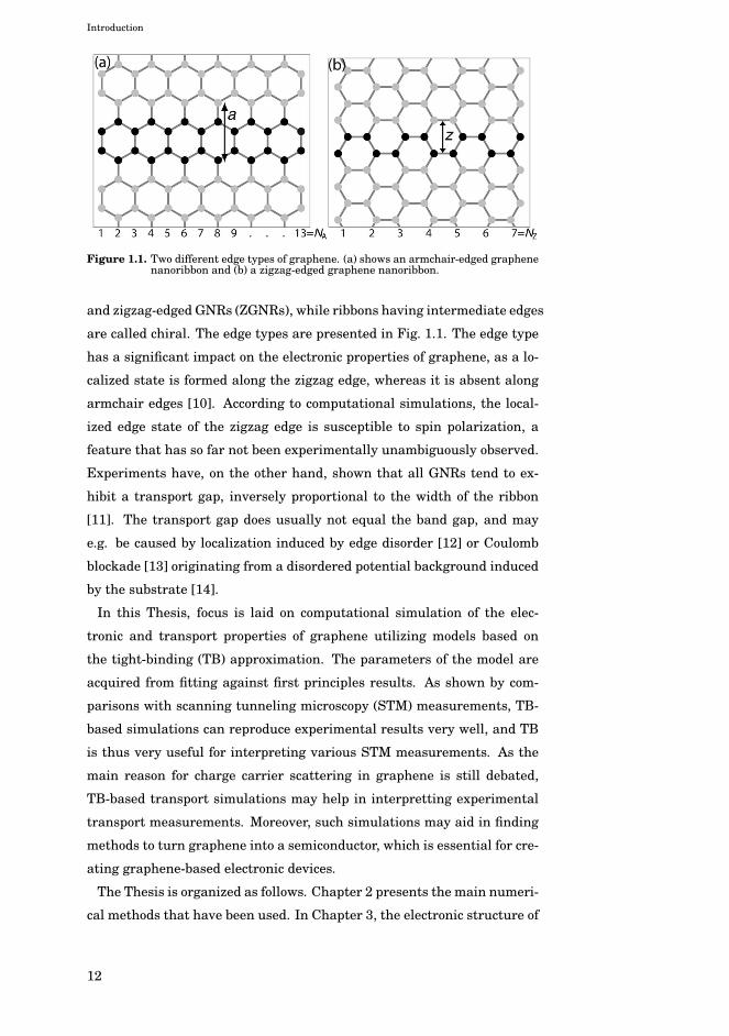
Introduction
Figure 1.1. Two different edge types of graphene. (a) shows an armchair-edged graphenenanoribbon and (b) a zigzag-edged graphene nanoribbon.
and zigzag-edged GNRs (ZGNRs), while ribbons having intermediate edges
are called chiral. The edge types are presented in Fig. 1.1. The edge type
has a significant impact on the electronic properties of graphene, as a lo-
calized state is formed along the zigzag edge, whereas it is absent along
armchair edges [10]. According to computational simulations, the local-
ized edge state of the zigzag edge is susceptible to spin polarization, a
feature that has so far not been experimentally unambiguously observed.
Experiments have, on the other hand, shown that all GNRs tend to ex-
hibit a transport gap, inversely proportional to the width of the ribbon
[11]. The transport gap does usually not equal the band gap, and may
e.g. be caused by localization induced by edge disorder [12] or Coulomb
blockade [13] originating from a disordered potential background induced
by the substrate [14].
In this Thesis, focus is laid on computational simulation of the elec-
tronic and transport properties of graphene utilizing models based on
the tight-binding (TB) approximation. The parameters of the model are
acquired from fitting against first principles results. As shown by com-
parisons with scanning tunneling microscopy (STM) measurements, TB-
based simulations can reproduce experimental results very well, and TB
is thus very useful for interpreting various STM measurements. As the
main reason for charge carrier scattering in graphene is still debated,
TB-based transport simulations may help in interpretting experimental
transport measurements. Moreover, such simulations may aid in finding
methods to turn graphene into a semiconductor, which is essential for cre-
ating graphene-based electronic devices.
The Thesis is organized as follows. Chapter 2 presents the main numeri-
cal methods that have been used. In Chapter 3, the electronic structure of
12
Introduction
graphene is discussed. In Publication I, TB models for graphene are pre-
sented, suitable for both band structure and electronic transport calcula-
tions. In Publications II to V, both TB and density-functional-theory-based
results are compared against scanning tunneling microscopy measure-
ments of graphene-based systems. Chapter 4 deals with electronic trans-
port in graphene. In Publication VI, two TB-based methods for transport
calculations are compared, namely the Landauer-Büttiker and the Kubo-
Greenwood formalisms, and efficient methods to implement the Kubo-
Greenwood method on GPUs are presented. Publication VIII deals with
how the localization length of a mesoscopic conductor can be obtained us-
ing the Kubo-Greenwood formalism. In Publication VII, Fabry-Pérot in-
terference in a graphene device is studied both experimentally and com-
putationally. In Publication IX and Publication X an effective scattering
cross section formalism for transport calculations in graphene is studi-
ed. In Publication XI, electronic transport in the quantum Hall regime is
studied, and in Publication XII transport results for notched spin-polarized
ZGNRs are presented.
13

Introduction
14

2. Computational methods
2.1 The tight-binding model
The TB model is a very simple model for electronic structure calculations.
Its advantage over ab initio methods is its low computational cost, which
enables simulating systems that are large enough to contain even millions
of atoms. Despite the simplicity of the model, it is relatively accurate,
especially for carbon-based materials such as graphene.
In the TB model, the total wave function of a system is approximated to
be a linear combination of atomic orbitals centered on the atomic sites of
the lattice. The model can be further simplified by only simulating charge
carriers with energies close to the Fermi level. For example, each carbon
atom has four valence electrons, but in graphene they are arranged in
three planar σ bonds and a single π bond, distributed equally over the
neighbors. In graphene, the electronic states closest to the charge neu-
trality point (CNP) correspond to the π bonds, and thus it is sufficient to
model only a single π electron per atomic site [15].
The Hamiltonian for an electron occupying a lattice point can be written
as
H = Hat +ΔV (r), (2.1)
where Hat is the atomic Hamiltonian and ΔV (r) is the potential caused
by all the other ions of the lattice. Let ψn(r) denote an eigenstate of the
atomic Hamiltonian, i.e. an atomic orbital, thus satisfying
Hatψn(r) = Enψn(r). (2.2)
An electronic state Ψ(r) localized at the atomic site can be expressed as a
15
Computational methods
linear combination of the atomic orbitals, according to
Ψ(r) =∑n
bnψn(r), (2.3)
where bn denotes the expansion coefficients. These electronic states can
further be expanded to form a Bloch wave that satisfies the periodicity of
the lattice, defined by the lattice vectors R,
Φ(r) =∑R
exp(ik · r)Ψ(r−R), (2.4)
where k is the crystal momentum. This can be taken to be the solution of
a Schrödinger equation with the Hamiltonian defined by Eq. 2.1, i.e.
HΦ(r) = HatΦ(r) + ΔV (r)Φ(r) = E(k)Φ(r). (2.5)
By multiplying with ψ∗(r) and integrating over r this turns into the ma-
trix equation ∑n
A(k)mnbn = E(k)∑n
B(k)mnbn, (2.6)
where the matrices A and B are defined as
A(k)mn =∑R
exp(ik ·R)
∫ψ∗m(r)Hψn(r−R)dr (2.7)
and
B(k)mn =∑R
exp(ik ·R)
∫ψ∗m(r)ψn(r−R)dr. (2.8)
By inserting Eq. 2.1 and using the orthonormality of the atomic orbitals
an equivalent expression can be obtained, i.e.
∑n
C(k)mnbm = (E(k)− Em)∑n
B(k)mnbn, (2.9)
where the elements of the matrix C(k) are defined as
C(k)mn =∑R
exp(ik ·R)
∫ψ∗m(r)ΔV (r)ψn(r−R)dr. (2.10)
As an abbreviation, the integrals can be denoted as
s(R) =
∫ψ∗(r)ψ(r−R)dr (2.11)
16
Computational methods
and
t(R) =
∫ψ∗(r)ΔV (r)ψ(r−R)dr. (2.12)
The first integral is commonly called the overlap integral, and the second
the hopping integral, as it can be thought to represent the energy cost for
a charge carrier to hop from one lattice site to another. The values of both
t(R) and s(R) greatly depend on the discrete variable R. The wave func-
tion Ψ(r) decays exponentially away from the lattice site with R = 0, and
it is often approximated that s = 0 if R �= 0, which creates an orthogonal
TB model. If R = 0, s(R) = 1. In the simplest tight binding model, the
hopping integral is assumed to take nonzero values only between near-
est neighbors, but also further than nearest neighbor interactions may be
considered.
2.2 The Hubbard model
The basic TB model describes non-interacting particles. Thus, in order to
simulate phenomena like spin polarization, one may add an interaction
term into the Hamiltonian. The so-called Hubbard model provides one of
the simplest ways to implement this, by taking into account the Coulomb
repulsion of the electrons only in the case of the electrons occupying the
same lattice site. This allows the study of the basic magnetic properties of
graphene-based systems. In the second quantization notion, the Hubbard
Hamiltonian can be written as
H =∑i,j
ti,jcic†j + U
∑i,σ
ni,σni,−σ, (2.13)
where c and c† are the electronic creation and annihilation operators, i
and j are site indices, and U is a parameter describing the strength of
the electronic on-site Coulomb repulsion. ni,σ and ni,−σ are the number
operators for the opposite spins σ and −σ. Despite the simplicity of the
Hubbard model, it can only be used to study systems that contain a hand-
ful of lattice sites, as the dimension of the many-body Hilbert space grows
roughly exponentially with system size. In order to study larger systems,
one may apply the mean field approximation, which effectively reduces
the interparticle interactions into interactions between a single particle
and and a field caused by all the other particles. It is derived as follows.
17

Computational methods
The fluctuation of the spin density from the mean value 〈ni,σ〉 is given by
Δni,σ = 〈ni,σ〉 − ni,σ, (2.14)
and the Hubbard term can thus be written as
U∑i,σ
(〈ni,σ〉 −Δni,σ)(〈ni,−σ〉 −Δni,−σ)
= U∑i,σ
(〈ni,σ〉〈ni,−σ〉 − 〈ni,σ〉Δni,−σ − 〈ni,−σ〉Δni,σ +Δni,σΔni,−σ).(2.15)
If the fluctuations are assumed to be small, the last term can be ignored.
After re-insertion of Eq. 2.14, the final form of the mean field Hubbard
Hamiltonian is acquired
H =∑i,j
ti,jcic†j + U
∑i,σ
(ni,σ〈ni,−σ〉+ ni,−σ〈ni,σ〉 − 〈ni,σ〉〈ni,−σ〉). (2.16)
As the Hamiltonian is needed to obtain the spin occupancies, it must be
solved self-consistently, starting with a randomly chosen spin distribu-
tion. As the converged result does not necessarily represent the ground
state, the computations need to be performed several times in order to
ensure that the ground state is found. After a converged ground state re-
sult has been acquired, the spin polarization pi at a lattice site i may be
calculated using the expression
pi =〈ni,σ〉 − 〈ni,−σ〉〈ni,σ〉+ 〈ni,−σ〉 . (2.17)
2.3 Density functional theory
The density functional theory (DFT) is an ab initio model that can be used
to compute the electronic structure of various systems. The foundations
of the DFT are laid by the two Hohenberg-Kohn theorems [16]. According
to the first one, the electronic density n uniquely determines the elec-
tronic properties of the system. Thus the number of degrees of freedom of
an N -particle system may be reduced from three times N to three. The
second Hohenberg-Kohn theorem states that the exact ground state min-
imizes the total energy, which is a functional of the electronic density.
In order to compute n, the so-called Kohn-Sham framework is used [17].
The framework is based on a Hamiltonian for non-interacting electrons,
18

Computational methods
which move in an effective potential background that takes into account
electron-electron interactions. The potential background is a functional
of the electronic density, although the choice of the functional is not com-
pletely unambiguous.
The DFT is applied by constructing the Kohn-Sham (K-S) Hamiltonian
[17]. It can be used to solve the total energy of the system, as well as the
self-consistent electronic density. However, the physical meaning of the
individual K-S eigenvalues and eigenstates has not been rigorously jus-
tified, although the energy of the highest occupied eigenstate has been
shown to be related to the first ionization energy [18]. Nevertheless,
as comparisons with scanning tunneling microscopy measurements have
shown, the individual K-S eigenstates bear a clear similarity with exper-
imental dI/dV maps.
2.4 Methods for computing the local density of states
The local density of states (LDOS) is defined as the number of electronic
states per volume and energy element. Scanning tunneling microscopy
provides a method to measure the LDOS experimentally, and experimen-
tal results may be directly compared to the simulated LDOS maps. To
obtain the LDOS maps, one may compute the retarded Green’s function
for the system, i.e.
G(E) =1
EI −H + iη, (2.18)
where I is the identity matrix and η a small positive number, whose mag-
nitude determines the broadening of the states in energy. The LDOS at
atomic site i can be obtained from the diagonal elements of the Green’s
function using the expression
ρi(E) = − 1
πIm Gii(E) (2.19)
Alternatively, if a finite or a periodic system is studied, one may directly
diagonalize the corresponding Hamiltonian. To compare the discrete eigen-
value spectrum obtained from diagonalization with experimental results,
each eigenvalue is be broadened using a Lorentzian function, which cre-
ates equivalent results compared with the Green’s function method. One
has to note that the experimentally measured values are affected by the
lifetime broadening of the charge carriers, as well as the layout of the
experimental setup, and the broadening parameter may simply be fitted
19

Computational methods
with the experimental results. In the case of small finite systems, one
may obtain a local density of states by means of exact diagonalization of
a many-body Hamiltonian. In Publication II and Publication III, the local
densities of states for finite seven-atom wide AGNRs, given by the mean-
field Hubbard model, the full many-body Hubbard model, and the DFT,
are compared with experimental results.
In addition to the TB model, the LDOS can also be approximated using a
continuum model. In principle, the correct continuum model for graphene
is the Dirac equation, which takes into account all the degrees of freedom
of the charge carriers. However, it has been demonstrated that away from
the zigzag edges, the LDOS of a hexagonal graphene flake can be fairly
accurately estimated also using the scalar Klein-Gordon equation [19]
−v2F�2∇2ψi = E2
i ψi, (2.20)
where vF is the Fermi velocity of graphene.
2.5 Methods for transport calculations
2.5.1 The Landauer-Büttiker formalism
The Landauer-Büttiker formalism is a very commonly used method to
compute the conductance of a device coupled to two or multiple contacts.
An introduction to the formalism can be found e.g. in Ref. [20]. In the
Landauer-Büttiker approach, the contacts are modeled as ballistic semi-
infinite leads. The conductance is obtained from the transmission func-
tion T (E), which for a single mode-system equals the probability of a
charge carrier to transmit from one contact to another. If there are several
transport modes involved, the transmission function equals the sum of the
transmission probabilities for the different modes. The retarded Green’s
function for a system attached to two leads is given by the expression
G(E) = [EI −H − ΣL(EL)− ΣR(ER)]−1 , (2.21)
where I is the unit matrix and ΣL/R(EL/R) is the self-energy of the corre-
sponding lead. The Fermi energy EL/R of the leads can be set to the same
value as in the device, E, or to an arbitrary value. In this work, it is set
either to E or to a fixed value of 1.5 eV, which is used to simulate metallic
20

Computational methods
contacts with a high number of propagating modes. The self energy mat-
rices may be obtained through different methods, e.g., using an iterative
method [21]. The matrices ΓL/R, that describe the coupling to the leads,
are obtained from
ΓL/R = i[ΣL/R − Σ†
L/R
], (2.22)
and the conductance is then computed using
G(E) = G0Tr[ΓRG(E)ΓLG†(E)
], (2.23)
where G0 ≡ 2e2/h is the quantum of conductance.
2.5.2 The Kubo-Greenwood method
The Kubo-Greenwood (KG) method is an alternative method to compute
the conductivity of a phase-coherent conductor [22, 23]. In the Kubo-
Greenwood formalism, the conductivity is acquired from the expectation
value of the mean square displacement (MSD) of the charge carriers.
Thus, as opposed to the Landauer-Büttiker formalism, contacts or leads
are not modeled. In Publication VI, it is presented how the KG method
can be implemented on graphics processing units, together with a com-
parison with results obtained using the Landauer-Büttiker approach.
The KG formalism is presented in detail in Publication VI, but below is
a short summary of the main methods. In the time-dependent Einstein
formula [24, 25, 26, 27, 28, 29, 30, 31], which can be derived from the KG
formula, the zero-temperature electrical conductivity at Fermi energy E
and correlation time t may be obtained as a time-derivative of the MSD
ΔX2(E, t), i.e.,
σ(E, t) = e2ρ(E)d
2dtΔX2(E, t), (2.24)
where
ΔX2(E, t) =Tr
[2Ωδ(E −H) (X(t)−X)2
]Tr
[2Ωδ(E −H)
] , (2.25)
and
ρ(E) = Tr[2
Ωδ(E −H)
](2.26)
is the density of states (DOS) with spin degeneracy included. X(t) =
exp(iHt/�)X exp(−iHt/�) is the position operator X given in the Heisen-
berg representation. In the case graphene simulations, Ω is the area of
the simulation cell.
The KG method has several advantages over the Landauer-Büttiker for-
21

Computational methods
malism. Perhaps most importantly, one can achieve linear scaling of the
computational cost with regard to the simulation cell size, whereas in the
GF method the computational cost scales cubically with the width of the
system. On the other hand, the KG method has also some drawbacks. Ob-
viously one of them is that the effect of contacts cannot be modeled, only
the intrinsic properties of the material. Additionally, in a quasi-1D sys-
tem, the individual transmission values for different conduction channels
cannot be acquired.
22

3. The electronic structure of graphene
3.1 Band structure
The π electron bands of two-dimensional graphene contain valleys hav-
ing linear dispersion and being located at the corners of the hexagonal
Brillouin zone. Two of the valleys are nonequivalent, creating a valley de-
gree of freedom for the charge carriers. Due to these features, the charge
carriers behave as massless Dirac fermions close to the CNP. Figure 3.1
shows the band structure of graphene given by a nearest-neighbor TB cal-
culation and Figure 3.2 shows a zoom-in on the band structure at one of
the valleys. The band structure of graphene can be simulated using the
DFT, and the TB parameters can then be optimized against the results.
In Publication I different sets of TB parameters are presented, suitable
for modeling both the band structure and electronic transport properties
of GNRs.
As shown in Publication I and Ref. [15], an extended TB model is able
to provide results that are very similar to those acquired from much more
time consuming ab initio calculations. The results still depend highly on
the parameters that have been selected, and different sets of parameters
can reproduce the band structure of AGNRs and ZGNRs with different de-
grees of accuracy. In Publication I also electronic transport results given
by TB and DFT are compared, more of which will be discussed in Chap-
ter 4.
If graphene is cut into ribbons, the 2D electronic bands become split into
sub-bands due to transverse quantization of the energy. In AGNRs, this
leads to the formation of a band gap that is inversely proportional to the
width of the ribbon [32]. This is illustrated in Fig. 3.3, which shows the
band structure of a 14-AGNR, as well as the band gaps of a range of AG-
23

The electronic structure of graphene
Figure 3.1. The valence band of 2D graphene, computed using a nearest-neighbor tight-binding model.
Figure 3.2. A zoom-in on the band structure of graphene around one of the Dirac points.
24

The electronic structure of graphene
Figure 3.3. Comparison between DFT (gray) and TB (black) results for armchairgraphene nanoribbons. The left panel shows the band structure of a 14-AGNR, and right panel a comparison of the calculated the band gaps ofnarrow AGNRs of different widths. The upper panel compares a nearest-neighbor orthogonal TB model results with the DFT results, and the lowerpanel a third-nearest neighbor non-orthogonal TB model results with theDFT results.
NRs with different widths. The gray bands and circles have been obtained
using DFT simulations, whereas the black ones are from TB calculations.
The upper row compares a nearest-neighbor orthogonal TB model with a
DFT result, whereas the lower row compares an optimized third-nearest
neighbor non-orthogonal TB model with the same DFT result. In the DFT
results, the local density approximation has been applied. The parame-
ters are given in Publication I. It can be seen that the nearest-neighbor
TB model predicts one third of the ribbons to be metallic, whereas a model
with hoppings up to third-nearest neighbors correctly predicts a gap for
all AGNRs.
In addition to a different quantization direction, ZGNRs differ from AG-
NRs by exhibiting a special localized edge state that arises due to the
edge topology. Computational results for ZGNRs are shown in Fig. 3.4,
where the black lines indicate results from a third-nearest neighbor non-
orthogonal mean-field Hubbard model. Interestingly, the localized edge
state is located at the CNP and causes all such ribbons to be metallic, in
the absence of electron-electron interactions. However, as the DFT or the
application of the mean-field Hubbard model show, a gap may open up.
25
The electronic structure of graphene
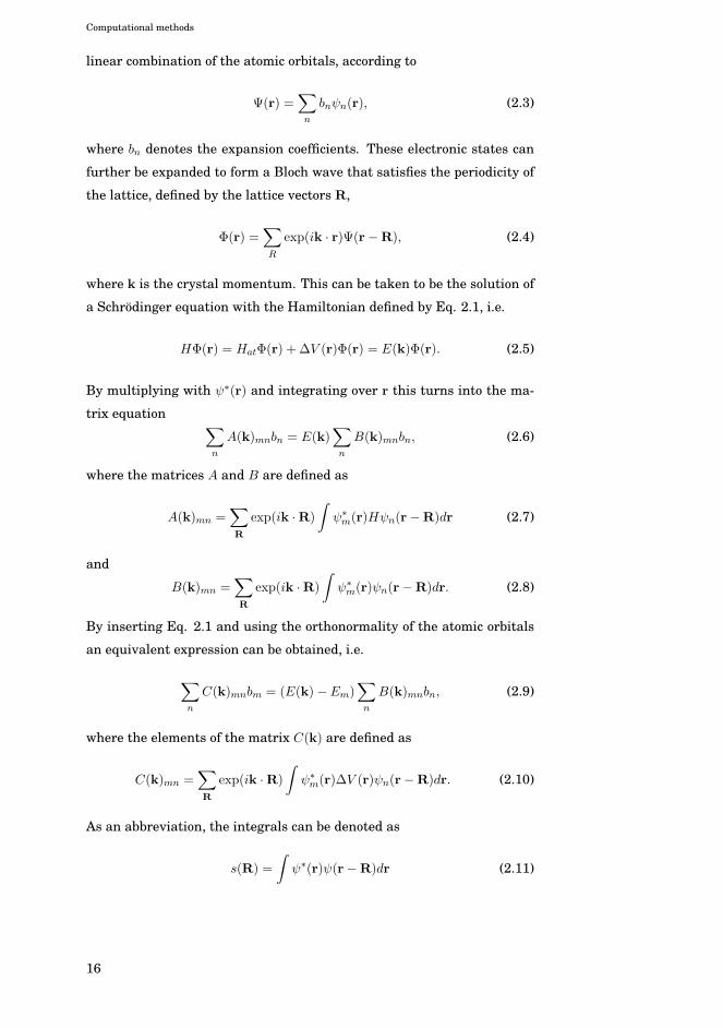
Figure 3.4. Comparison between DFT (gray) and TB (black) results for zigzag graphenenanoribbons. The left panel shows the band structure of a 14-ZGNR, andright panel a comparison of the calculated the band gaps of narrow ZGNRsof different widths. The upper panel compares a nearest-neighbor orthogonalTB model results with the DFT results, and the lower panel a third-nearestneighbor non-orthogonal Hubbard model results with the DFT results.
The opening of the gap depends strongly on the doping of the ribbon, as
the simulations predict that only charge-neutral ribbons will have a gap.
Thus best comparison with DFT results can be achieved by including a
Hubbard mean-field and a parameter set covering electron hoppings and
overlaps up to third-nearest neighbors. However, as an overlap matrix
complicates the calculations and increases the number of free parame-
ters, without adding significant qualitative detail near the Fermi level,
it is not essential in a minimal model. On the other hand, second- and
third-nearest neighbor hoppings may be valuable additions in the model.
Second-nearest neighbor hopping results in electron-hole asymmetry as
well as increased trigonal warping of the conical band structure, whereas
third-nearest neighbor hopping causes a band gap in all AGNRs [33]. A
TB model with hoppings up to third-nearest neighbors thus is able to ac-
curately reproduce both the ab initio band structures and transmission
properties of GNRs. The addition Hubbard mean field is relevant mainly
for systems containing zigzag-shaped edges, as neither bulk graphene nor
armchair-shaped edges exhibit spin-polarization with reasonable values
of U .
26

The electronic structure of graphene
Ab initio results predict that in AGNRs the edge bond lengths are about
3.5 % shorter than those in the middle of the ribbon, leading to increased
overlap and hopping between the corresponding atomic sites. To take this
into account in the TB model, it has been proposed that t1 can be increased
by 6–12 % at the edges [32, 34]. The band gaps of AGNRs can be calcu-
lated with even better accuracy by taking into account edge relaxation. In
ZGNRs the edge relaxation is weaker and modifying the nearest neighbor
hopping values to take it into account causes only negligible changes in
the band structure.
3.2 Comparisons between simulations and scanning tunnelingmicroscopy results
In scanning tunneling microscopy (STM), an atomically sharp tip is placed
on top of a sample, and the electric current is measured after the appli-
cation of a bias voltage between the sample and the tip. Such a system
conducts through quantum-mechanical tunneling of charge carriers. The
measured results are affected by the finite lifetime of the charge carriers
in the sample, which causes a broadening in energy. In such a case, the
tunneling current is proportional to the LDOS of the sample close to the
tip. According to the Tersoff-Hamann theory of STM [35],
I ∝∑ν
|ψν(r0)|2 σ(Eν − EF ), (3.1)
where ψv(r0) is the amplitude of the νth eigenstate at r0 and Eν is the
corresponding energy eigenvalue. Thus STM provides a method to study
the electronic structure of a sample, as the measured dI/dV maps provide
an estimate for the local density of states at the tip position.
In Publication IV, the electronic structure of hexagonal graphene nano-
flakes on top of an Ir(111)-surface were studied through STM measure-
ments and computational simulations. The measurements yielded stand-
ing wave patterns, whose complexity increased with increasing energy, as
shown as in Fig. 3.5 (a). This indicates behavior analogous to a particle-in-
a-box-problem. To simulate the patterns, an atomistically exact TB-based
model was created, and the eigenstates were solved through exact diago-
nalization of the TB Hamiltonian. The results are presented in Fig. 3.5 (c),
whereas predictions from a simple continuum model based on the Klein-
Gordon equation are shown in Fig. 3.5 (d).
27

The electronic structure of graphene
b
a e
c
d
-0.25V
-0.140eV
-0.175eV
-0.30V
-0.200eV
-0.225eV
-0.35V
-0.245eV
-0.280eV
-0.40V
-0.290eV
-0.335eV
-0.55V
-0.445eV
-0.470eV
0.0 -0.1 -0.2 -0.3 -0.4 -0.5 -0.60.0
-0.1
-0.2
-0.3
-0.4
-0.5Klein-Gordontight-binding
E(e
V)
-0.45V
-0.350eV
-0.380eV
STM bias voltage (V)
Figure 3.5. (a) Atomically resolved image of a graphene flake on Ir(111). (b) STM mapsof graphene nanoflakes on Ir(111), taken at different bias voltages. (c) and (d)show the corresponding TB and continuum model (based on the Klein-Gordonequation) maps. (e) Correspondence between experimental bias voltages andthe energy values of the best fitting theoretical simulations.
Figure 3.6. Comparison of the low-energy eigenstates (left) and eigenvalues (right) of afinite 7-atom wide AGNR obtained using three different methods. The differ-ent markers link the eigenstates and the corresponding eigenvalues.
28

The electronic structure of graphene
Figure 3.7. Comparison between measured (top) and simulated (bottom) electronic statesof finite armchair-edged graphene nanoribbons. These simulations have beenperformed using the density functional theory, although tight-binding simu-lations yielded very similar results. In the simulations, the tip is assumed tobe a mix between a p-type and an s-type orbital.
Similar confined states have been found also in other studies [36, 37, 38].
In particular, Altenburg et al. [38] argued that the observed states may
be examples of confinement of the Ir(111) surface state. This view is sup-
ported by ab initio calculations, suggesting that the Ir edge state decays
slower in the perpendicular direction than bulk graphene states. This can
be explained by the fact that the Fermi surface of graphene is located in
the vicinity of the K points of the Brillouin zone, whereas the edge state
of Ir resides close to the Γ point. On the other hand, one has to note
that finite graphene flakes on the Ir(111) substrate were not simulated
in Ref. [38] and may exhibit different behavior, especially if their size is
small.
Computational results were compared against STM measurements also
in Publication II. Finite, seven dimer wide armchair nanoribbons were
formed from precursor molecules using a bottom-up technique presented
in Ref. [39]. STM imaging and scanning tunneling spectroscopy (STS)
measurements of the ribbons was performed, and compared against DFT
and Hubbard model results. It was noted that both ab initio and Hubbard
model calculations can reproduce the low-energy dI/dV maps, measured
using both s- and p-type tips. This is illustrated in Fig. 3.6, which com-
pares the theoretical results with each other, and in Fig. 3.7, which com-
pares DFT results with experimental measurements. The simulations are
discussed in more detail in Publication III. However, simulating the STS
spectra requires a model which takes into account phonon-assisted tun-
neling, more of which is discussed in Section 4.6.
29

The electronic structure of graphene
Figure 3.8. Comparison between a measured (left) and a simulated (right) STM map ofthe graphene - hexagonal boron nitride interface state. The simulated imagehas been calculated using a third-nearest neighbor TB model. The graphenelattice is indicated by the hexagonal network, whereas the positions of theboron atoms are indicated by orange circles and the positions of the nitrogenatoms by blue circles.
In Publication V the interface between graphene and hexagonal boron
nitride (h-BN) was studied. STM measurements showed a series of ob-
long spots along the interface at low-bias measurements, a feature which
according to the simulations matches an interface where the boron and
carbon atoms are bonded together. A comparison of the experimental map
with a TB simulation is shown in Fig. 3.8. The orthogonal TB model in-
cludes hoppings up to third-nearest neighbors, with the hopping param-
eters being the same for both the graphene and h-BN lattices. h-BN is
simulated through onsite potentials on the B and N atoms. The hopping
parameters between the graphene and h-BN lattices have been reduced,
as this gives a best match with a DFT-based band structure. This is fur-
ther motivated by DFT predicting longer bond lengths between the two
different lattices compared to the intralattice bond lengths. According
to both DFT and TB simulations, an interface formed by nitrogen atoms
bonding to the graphene edge would look clearly different, as shown in
Publication V. Thus it was concluded that the observed interfaces are
formed by boron bonding with the carbon atoms along the edge of the
graphene lattice.
30

4. Electronic transport in graphene
The conductance of a device is measured by attaching two or multiple
probes, and measuring the current as a function of bias voltage Vb. The
conductance is simply obtained from G = dI/dVb. In this Thesis, only
two-probe systems are considered. The properties of electronic transport
depend heavily on characteristic length scales of the system. The phase
coherence length determines the length scale for quantum-mechanical in-
terference phenomena. Scattering by defects with no internal degrees
of freedom is elastic, and results in the conservation of the phase of the
charge carriers. On the other hand, scattering by other charge carriers or
phonons can result in momentum transfer and phase decoherence. The
length that sets the scale between scattering events is called the mean
free path l, whereas the elastic mean free path le sets the scale between
elastic scattering events. When l is smaller than the phase coherence
length, the corresponding system can be called mesoscopic, and phenom-
ena due to quantum-mechanical interference can be observed. When the
size of the system is smaller or at most of the same order as l, the charge
carriers behave ballistically or quasi-ballistically.
4.1 Ballistic transport and Fabry-Pérot resonances
One of the most prominent features of graphene is the low amount of
disorder present in the material. This is especially true for exfoliated
graphene, which may exhibit charge carrier mobilities exceeding 100 000
Vs/cm2 [9] and ballistic transport in samples that are up to several micro-
meters long [40]. In 2D graphene, the conductivity σ of a ballistic device
is infinite, whereas in a two-terminal device, transverse quantization re-
sults in a finite number of transport modes that limit the conductance to
G = G0M , where M is the number of modes. The Landauer-Büttiker for-
31

Electronic transport in graphene
malism based on Green’s functions yields correctly the quantized conduc-
tance of a ballistic graphene device, whereas the Kubo-Greenwood method
experiences numerical inaccuracies, as discussed in Publication VI and
Ref. [28].
One of the peculiar features of graphene is that ballistic devices with
W L exhibit a finite minimum conductivity, even at the Dirac point
where the density of states is zero. Theoretically, a minimum conductivity
of 4e2/πh can be derived, resulting from evanescent modes extending into
bulk graphene from the contacts [8, 41]. However, experimental results
have yielded larger values than this, which has been attributed to the
presence of long-ranged potential disorder due to the substrate [42].
In a ballistic device, scattering of charge carriers is mainly induced by
the edges of the sample and the device-contact interfaces. If the system
is sufficiently phase coherent, this leads to Fabry-Pérot-type interference
of the charge carriers. This was studied in Publication VII, where ex-
perimental and simulated results for a suspended graphene device con-
tacted to two metallic leads were compared. According to a particle-in-a-
box model for charge carriers with linear dispersion, the conductance of
a device with dimensions W × L should show resonances approximately
located at [43, 44]
EqL,qW∼= ±
√E2
L(qL + δL)2 + E2
W (qW + δW )2, (4.1)
where EL ≡ hvF /2L and EW ≡ hvF /2W . The values of the constants
δL and δW depend on the details of the interfaces or edges [43], and the
quantum numbers qL and qW label longitudinal and transverse modes,
respectively. Therefore the resonances should roughly occur at intervals
of EL and EW , with the longitudinal resonances occurring due to bunching
of single-mode transverse resonances, thus being of a multimode nature.
Using a nearest-neighbor TB transport model, a device connected to two
semi-infinite graphene leads at a constant doping of 1.5 eV was simulated.
Figure 4.1 (a) shows the resulting conductance curve, (b) the correspond-
ing dG/dμ0 map and (c) its Fourier transform. Here μ0 is a zero-bias chem-
ical potential, roughly corresponding to the gate voltage of an experimen-
tal setup. The vertical lines in (a) indicate the positions of the resonances
given by Eq. 4.1, whereas the solid and dashed lines in (c) indicate the
locations of 1/2EL and W/L(1/2EL), respectively.
The experimentally measured dI/dV curve showed a similar behavior
32
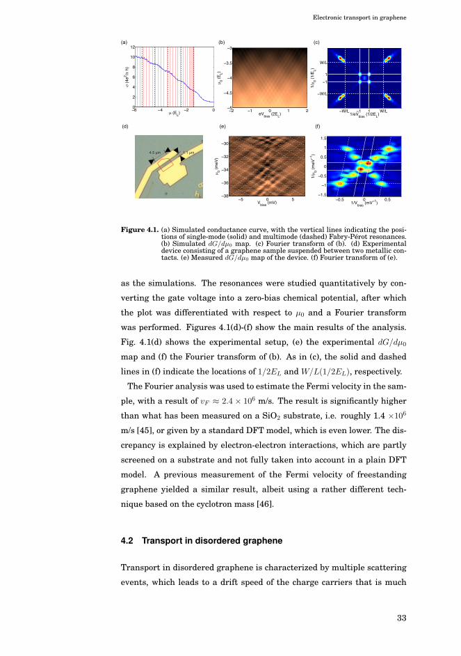
Electronic transport in graphene
(b) (c)(a)
μμ
μμ
(e) (f)(d)
Figure 4.1. (a) Simulated conductance curve, with the vertical lines indicating the posi-tions of single-mode (solid) and multimode (dashed) Fabry-Pérot resonances.(b) Simulated dG/dμ0 map. (c) Fourier transform of (b). (d) Experimentaldevice consisting of a graphene sample suspended between two metallic con-tacts. (e) Measured dG/dμ0 map of the device. (f) Fourier transform of (e).
as the simulations. The resonances were studied quantitatively by con-
verting the gate voltage into a zero-bias chemical potential, after which
the plot was differentiated with respect to μ0 and a Fourier transform
was performed. Figures 4.1(d)-(f) show the main results of the analysis.
Fig. 4.1(d) shows the experimental setup, (e) the experimental dG/dμ0
map and (f) the Fourier transform of (b). As in (c), the solid and dashed
lines in (f) indicate the locations of 1/2EL and W/L(1/2EL), respectively.
The Fourier analysis was used to estimate the Fermi velocity in the sam-
ple, with a result of vF ≈ 2.4 × 10⁶ m/s. The result is significantly higher
than what has been measured on a SiO2 substrate, i.e. roughly 1.4 ×10⁶
m/s [45], or given by a standard DFT model, which is even lower. The dis-
crepancy is explained by electron-electron interactions, which are partly
screened on a substrate and not fully taken into account in a plain DFT
model. A previous measurement of the Fermi velocity of freestanding
graphene yielded a similar result, albeit using a rather different tech-
nique based on the cyclotron mass [46].
4.2 Transport in disordered graphene
Transport in disordered graphene is characterized by multiple scattering
events, which leads to a drift speed of the charge carriers that is much
33
Electronic transport in graphene
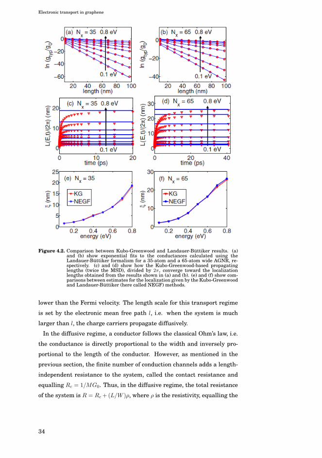
Figure 4.2. Comparison between Kubo-Greenwood and Landauer-Büttiker results. (a)and (b) show exponential fits to the conductances calculated using theLandauer-Büttiker formalism for a 35-atom and a 65-atom wide AGNR, re-spectively. (c) and (d) show how the Kubo-Greenwood-based propagatinglengths (twice the MSD), divided by 2π, converge toward the localizationlengths obtained from the results shown in (a) and (b). (e) and (f) show com-parisons between estimates for the localization given by the Kubo-Greenwoodand Landauer-Büttiker (here called NEGF) methods.
lower than the Fermi velocity. The length scale for this transport regime
is set by the electronic mean free path l, i.e. when the system is much
larger than l, the charge carriers propagate diffusively.
In the diffusive regime, a conductor follows the classical Ohm’s law, i.e.
the conductance is directly proportional to the width and inversely pro-
portional to the length of the conductor. However, as mentioned in the
previous section, the finite number of conduction channels adds a length-
independent resistance to the system, called the contact resistance and
equalling Rc = 1/MG0. Thus, in the diffusive regime, the total resistance
of the system is R = Rc + (L/W )ρ, where ρ is the resistivity, equalling the
34

Electronic transport in graphene
inverse of the conductivity σ. Alternatively, this may be written as [20]
R(L) = Rc +RcL
le. (4.2)
In a diffusive system, the properties of the scatterers thus determine the
resistivity of the material.
In a mesoscopic system, corrections to the conductivity arise due to
quan-tum-mechanical interference phenomena. Depending on the mate-
rial and the type of scattering, interference can lead to either enhanced
or decreased backscattering due to constructive or destructive interfer-
ence between time-reversed propagation paths of the charge carriers. En-
hanced backscattering is called localization and decreased backscattering
antilocalization. In the presence of disorder that is able to cause scatter-
ing between the two independent valleys of the band structure, the charge
carriers experience localization, whereas when the disorder causes solely
intravalley scattering, the charge carriers experience antilocalization in-
stead. This is typical for graphene in the presence of long-ranged disorder,
and has been studied more extensively in e.g. Ref. [47]. Antilocalization
causes an increase of the conductivity, whereas localization causes a de-
crease. The sign of the localization correction to the conductance may be
probed using a weak magnetic field, as it will remove the time-reversal
symmetry and thus suppress quantum-mechanical interference.
When a phase-coherent system exhibiting localization is sufficiently long,
the charge carriers will become strongly localized. In the strongly local-
ized regime, the resistance grows exponentially instead of linearly with
the length of the system, i.e. R ∝ exp(L/ξ), with ξ being called the lo-
calization length. As a wave packet becomes localized, the mean square
displacement given by the KG method will converge to a finite value. In
Publication VIII it was shown that the converged MSD given by the Kubo-
Greenwood method is directly proportional to the localization length, with
the constant of proportionality being approximately 1/π. This is illus-
trated in Fig. 4.2, which compares KG results with those obtained using
Landauer-Büttiker calculations.
4.3 Effective scattering cross-section formalism
The scaling of the conductance of a mesoscopic conductor has been stud-
ied extensively for decades, see e.g. Ref. [20]. A useful quantity, called
35

Electronic transport in graphene
scattering or transport cross section, can be defined to characterize the
scatterers [48]. In Publication IX and Publication X an effective scatter-
ing cross section formalism was studied in order to test if single-defect
calculations may be used to predict the conductance of a mesoscopic sys-
tem with a large number of defects. This would enable one to directly
apply ab initio methods to compute the conductance of realistically sized
systems. The scattering cross section s is related to le and the concentra-
tion of impurities nimp through the relation
s(E) =1
nimple(E). (4.3)
In case of scattering by multiple defect types, the scattering cross sections
may be combined based on Matthiessen’s rule, which relates the elastic
mean free path to the individual elastic mean free paths that correspond
to different types of scattering through the reciprocal relation
1
le=
∑i
1
le,i(4.4)
In principle, Matthiessen’s rule could be utilized to also combine the effect
of inelastic scattering, but this does not necessarily lead to correct results,
as phonons may couple to the defects and impurities present in the lattice.
The mean free path may be used to obtain the conductance of a meso-
scopic quasi-1D system through scaling analysis. In the diffusive regime,
a relation between le and the transmission function can be derived [48]
using Eq. 4.2, i.e.
le(E) = dN〈T (E)〉
T0(E)− 〈T (E)〉 , (4.5)
where N is the number of scatterers and d the average distance between
them. 〈T (E)〉 is the ensemble averaged transmission function in the pres-
ence of scatterers and T0(E) the ballistic transmission function (equalling
the number of conduction channels). Equation 4.5 may be used to derive
the expression
s(E) = WT0(E)− 〈T (E)〉
N〈T (E)〉 , L � ξ(E), (4.6)
valid in the diffusive transport regime. In principle, with periodic bound-
ary conditions and transverse k-point sampling, one can compute s(E)
from single-defect calculations of systems that are small enough to be
simulated using the DFT. However, one has to be careful regarding the
36

Electronic transport in graphene
−1 0 110−6
10−4
10−2
100
102
104
E−EF [eV]
G [2
e2 /h]
Tcalc
(E)
Tpred
(E)
T0(E)
loc. OhmicOhmic
Figure 4.3. Comparison of the calculated and predicted transmission functions for a 30nm wide and 1000 nm long graphene nanoribbon with a 1% concentrationof Stone-Wales defects, 555777 defects and vacancies each. The predictedresult is based on a scaling approach utilizing single-defect scattering crosssections. The vertical bars divide the energy range into Ohmic (diffusive) andlocalized regimes.
condition L � ξ(E), as L is not clearly defined in the case of a single-
defect calculation. In practice, one needs to construct an expression for
s(E) also when the system is in the localized regime. To achieve this,
one can approximate that the transmission function is given by Ttyp(E) �T (E0) exp(−L/ξ(E)). This is valid when the contact resistance is negligi-
ble compared to the total resistance. Here Ttyp ≡ exp〈lnT (E)〉 is the typ-
ical transmission, which is computationally much easier to obtain than
the average transmission as the transmission values follow a log-normal
distribution in the localized regime [49]. The Thouless relation [50, 51],
i.e.
ξ(E) =M + 1
2le(E) (4.7)
relates ξ(E) length to le. Thus one can derive an expression for s(E) valid
in the localized regime:
s(E) =W (T0(E) + 1)〈ln[T0(E)/T (E)]〉
2N, L ξ(E). (4.8)
In Publication IX, scattering cross sections were calculated using a third-
nearest neighbor orthogonal TB model for a Stone-Wales defect, a 555777
defect and a vacancy. A Stone-Wales defect and a 555777 defect are struc-
tural defects [52], with the Stone-Wales defect being essentially a bond
rotation by 90◦ resulting in two pentagons and two heptagons embedded
in the honeycomb lattice. A 555777 defect is a relaxed form of a divacancy,
37
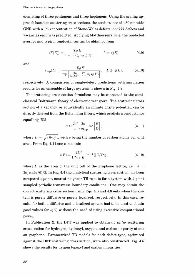
Electronic transport in graphene
consisting of three pentagons and three heptagons. Using the scaling ap-
proach based on scattering cross sections, the conductance of a 30 nm wide
GNR with a 1% concentration of Stone-Wales defects, 555777 defects and
vacancies each was predicted. Applying Matthiessen’s rule, the predicted
average and typical conductances can be obtained from
〈T (E)〉 = T0(E)
1 + L∑
i nisi(E), L � ξ(E) (4.9)
and
Ttyp(E) =T0(E)
exp[
2LT0(E)+1
∑i nisi(E)
] , L ξ(E), (4.10)
respectively. A comparison of single-defect predictions with simulation
results for an ensemble of large systems is shown in Fig. 4.3.
The scattering cross section formalism may be connected to the semi-
classical Boltzmann theory of electronic transport. The scattering cross
section of a vacancy, or equivalently an infinite onsite potential, can be
directly derived from the Boltzmann theory, which predicts a conductance
equalling [53]
σ ≈ 2e2
h
2n
πnimpln2
∣∣∣∣ED∣∣∣∣ , (4.11)
where D =√π�2v2F c, with c being the number of carbon atoms per unit
area. From Eq. 4.11 one can obtain
s(E) =2D2
Ω�vF |E| ln−2 (|E/D|) , (4.12)
where Ω is the area of the unit cell of the graphene lattice, i.e. Ω =
3a20 cos(π/6)/2. In Fig. 4.4 the analytical scattering cross section has been
compared against nearest-neighbor TB results for a system with k-point
sampled periodic transverse boundary conditions. One may obtain the
correct scattering cross section using Eqs. 4.6 and 4.8 only when the sys-
tem is purely diffusive or purely localized, respectively. In this case, re-
sults for both a diffusive and a localized system had to be used to obtain
good values for s(E) without the need of using excessive computational
power.
In Publication X, the DFT was applied to obtain ab initio scattering
cross section for hydrogen, hydroxyl, oxygen, and carbon impurity atoms
on graphene. Parametrized TB models for each defect type, optimized
against the DFT scattering cross section, were also constructed. Fig. 4.5
shows the results for oxygen (epoxy) and carbon impurities.
38

Electronic transport in graphene
−0.4 −0.2 0 0.2 0.40
2
4
6
8
10
E (eV)
s (n
m)
Figure 4.4. Comparison between the scattering cross section given by the Boltzmann for-malism, i.e. Eq. 4.12, indicated by the red line, and ensemble-averaged simu-lated results for a system with k-point sampled periodic transverse boundaryconditions. The circles have been obtained simulating a diffusive system andusing Eq. 4.6, whereas the triangles have been obtained simulating a local-ized system and using Eq. 4.8
−2 −1 0 1 20
0.2
0.4
0.6
0.8
1
1.2
1.4
1.6
1.8
2
σ (n
m)
Energy (eV)
TBDFT
Energy (eV)
n (%
)
le (nm)
−2 0 20.1
0.5
1
1.5
2
1
10
100
−2 −1 0 1 20
0.5
1
1.5
2
2.5
Energy (eV)
σ (n
m)
TBTBopt
DFT
Energy (eV)
n (%
)
le (nm)
−2 0 20.1
0.5
1
1.5
2
1
10
100
ex ex
ez
e1 e1
(a) (b)
Figure 4.5. Transport scattering cross sections for epoxy (a) and carbon impurities (b).The tight-binding parameters have been optimized to reproduce the DFT re-sult. The insets show the localization lengths as a function of impurity con-centration.
39

Electronic transport in graphene
4.4 Electronic transport in a magnetic field
Transport in graphene in a magnetic field has been studied in several
recent works [54, 55, 56]. If a sufficiently strong external perpendicular
magnetic field is applied on a conductor, the system may enter the quan-
tum Hall regime. In the quantum Hall regime, the bulk electronic states
in the system become quantized into so-called Landau levels (LLs) [20].
The quantum Hall effect is characterized by the off-diagonal conductance
of a multiprobe setup acquiring quantized values, whereas the longitudi-
nal resistance takes non-zero values only at the Landau levels. This is due
to the formation of edge channels that propagate in different directions at
the opposite edges of the system. Backscattering is possible only at the
Landau levels, where the presence of bulk states allows charge carriers to
scatter from one edge to another.
In Publication XI the conductance of a two-terminal device was stud-
ied in the quantum Hall regime. At high magnetic fields, the spin de-
generacy of the charge carriers becomes lifted. However, at lower field
strengths the degeneracy of the spins remains, which allowed the use of a
non-spin-polarized model. It was found that the type of disorder strongly
affects the width of the zeroth Landau level, located at the CNP. With
short-ranged potential disorder or vacancy-type defects, the zeroth LL
remains delta-function-like, whereas the other LLs become broadened.
With longer range potential disorder, the zeroth LL becomes wider, simi-
lar to the other LLs. Even if the chemical potential of the system is at a
LL, the current flowing through the device, given at zero temperature by
[20]
I(Vb) =2e
h
∫ EF+eVb/2
EF−eVb/2T (E)dE, (4.13)
is large when the bias window is broad compared to the width of the LL.
Thus in an experimental setup, a delta-function like zeroth LL will re-
sult in a low measured resistance peak. This agrees with experimental
conductance measurements of graphene on a SrTiO3 substrate [57]. The
resistance peak at the zeroth LL was found to decrease significantly as
a function of decreasing temperature. In SrTiO3, the dielectric constant
increases by an order of magnitude when the temperature decreases from
room to liquid helium temperature. Thus charge inhomogeneities be-
come strongly screened, which according to the simulations will reduce
the measured resistance. On the other hand, such a decrease can also be
attributed to a reduction in the effects of electron-electron interactions,
40

Electronic transport in graphene
Figure 4.6. Left hand panel: Resistance of AGNRs (top) and ZGNRs in the quantumHall regime with respect to the location of the zeroth LL E0, based on TBsimulations. Right hand panel: Corresponding band structures of pristineribbons.
that will also become more screened with increasing dielectric constant.
In Publication XI, it was also found that at the other LLs, the innermost
conduction channels become quickly completely localized in the presence
of disorder, whereas the other channels exhibit significantly longer local-
ization lengths. This will lead the four-terminal longitudinal resistance
(equalling the total longitudinal resistance minus the contact resistance)
to become pinned to fractional values of the resistance quantum at the
nonzero LLs, i.e.
R =h
2e22
4n2L − 1
, |nL| > 0, (4.14)
where nL is the Landau level index. Compared with the experimental
results in Ref. [7], the pinned values given by Eq. 4.14 differ by roughly
30% on average.
4.5 Spin-dependent transport
According to theoretical simulations, in a freestanding ZGNR at or very
close to half-filling, the edge states are spin-polarized. In the ground
41

Electronic transport in graphene
Figure 4.7. The spin polarization of a notched zigzag-edged graphene nanoribbon at halffilling. The lower panel shows the atomic structure of the ribbon.
Figure 4.8. Spin-dependent conductance for the notched system shown in Fig. 4.7 com-puted using (a) tight-binding and (b) DFT. Blue corresponds to the majorityspin and red to the minority spin.
42

Electronic transport in graphene
state, the opposite edges have opposite majority spin, resulting in sym-
metric transmission functions for both spin species. However, asymmetry
regarding the edges may result in a significantly spin-dependent conduc-
tance. In Publication XII, the conductance of a spin-polarized ZGNR with
a notch was computed. The structure of the device is shown in Fig, 4.7,
which also indicates the spin-polarization of the ground state, computed
using the mean-field Hubbard model. It turns out that the transmission
function is strongly spin-dependent, as shown in Fig. 4.8. Such a de-
vice could be used as a spin-filter. Similar ideas were also presented in
Ref. [58]. To realize a spin-filter, it is important that the chemical po-
tential of the system is close to the charge neutrality point and that the
applied bias voltage is small, as mean-field Hubbard and DFT calcula-
tions indicate that the ground state of a system with even a relatively
low level of doping is not spin-polarized. Additionally, the system must be
freestanding or located on a substrate that does not affect the edge state
or the spin-polarization.
4.6 Phonon-assisted transport
In this section, phonon-assisted tunneling during an STS measurement
is studied. In Publication II, experimental STS curves for finite AGNRs
on an Au(111) substrate were presented and compared against numeri-
cal simulations. Since such ribbons have zigzag-shaped termini, an edge
state was observed, as discussed in Section 2.3.2. However, despite good
match between simulated and measured STM maps, a simple LDOS-
based model did not reproduce the measured STS curves, which revealed
in addition to a prominent resonance close to the charge neutrality point,
a weaker resonance at positive bias. Interestingly, the weaker resonance
disappeared when a bond between the substrate and the opposite end
of the molecule was created. In order to explain this, several hypotheses
were tested, such as a change of the magnetic polarization or the charging
state of the molecule, or a change in the phonon-electron coupling. These
hypotheses are discussed in Publication II and Publication III. The best
explanation for the observed behavior was found to be that the weaker
resonance is a phonon replica of the edge state, with the induced bond
suppressing the electron-phonon coupling. This is supported by the fact
that the STS spectrum matches well a simulated result with parameter-
ized electron-phonon couplings.
43

Electronic transport in graphene
The computations are based on the methods presented in Refs. [59]. If
the end state is located at E0, the transmission function can be obtained
from
T (E) ∝∫ ∞
−∞dσ
�exp
(− Γ|σ|
2�+
2(E − E0 + λ)
�−
∑β
∣∣∣∣Mβ
�ωβ
∣∣∣∣2 [
(1 + 2N)ωβ)(1− cos(ωβσ)) + i sin(ωβσ)
]), (4.15)
where ωβ is the angular frequency of vibrational mode β, Γ = (Γtip +
Γsubstrate)/2 is the average coupling strength between the contacts, λ ≡∑β(M
2β/�ωβ) and Nωβ
is the Bose-Einstein occupation factor. The trans-
mission was computed using a two-phonon model with the electron-phonon
coupling strengths Mβ taken as free parameters and fitted to the mea-
sured STS curve, with the results shown in Fig. 4.9(a). However, the val-
ues of the parameters Mβ fit well in the range of ab initio results for the
electron-phonon coupling strengths in similar but isolated finite nanorib-
bons, as shown in Fig. 4.9(b).
44

Electronic transport in graphene
Figure 4.9. (a) Measured STS spectra at the left and right end central atoms of a finitegraphene nanoribbon. The red line is a simulated result taking into accountinteraction with two phonons, with parameters optimized against the mea-sured left end result. (b) Comparison between the optimized parameters forthe two phonons and DFT-based results for a similar but shorter molecule.The solid line shows the results with Gaussian broadening. (c) and (d) showconstant height STM maps taken at the elastic peak and the replica at 225meV, respectively, using a CO-terminated tip. (e) DFT simulation of a dI/dVmap at the CNP measured with a p-wave tip. A corresponding TB-simulationwould yield a very similar result. Scale bars, 0.5 nm.
45

Electronic transport in graphene
46
5. Summary
In this Thesis, the electronic properties of graphene has been studied,
with an emphasis on electronic transport. In Publication I, the parame-
ters of the tight-binding model were optimized to reproduce band struc-
ture and transport results given by the density functional theory. This
model was used in several of the other publications. In Publication II,
the local density of states of finite graphene nanoribbons on Au(111) was
studied both experimentally and through simulations. The measured and
simulated dI/dV maps agreed well with each other, but to obtain a good
match with the scanning tunneling spectrum for the end state of the
ribbon, phonon-assisted tunneling was needed to be taken into account.
Moreover, it was found that the phonon-assisted tunneling is suppressed
when the opposite end of the molecule becomes bonded to the substrate.
In Publication III, the simulations were presented in more detail, and it
was argued that spin-polarization does not seem to be a plausible reason
for the observed dI/dV spectrum. Publication III also presented direct
comparisons between tight-binding-based and computationally more ex-
pensive simulation results, as well as actual measurements, showing that
tight-binding gives very accurate results especially for the local density of
states of pristine molecules.
In Publication IV, the simulated local density of states for hexagonal
graphene nanoflakes was compared against STM measurements perfor-
med on an Ir(111) substrate. The results showed a good match between
simulations and experimental results, barring the lack of a localized edge
state in the experimental results, which can be explained by an interac-
tion between the edges and the substrate. The lower than expected Fermi
velocity may be explained by the experimental STM map being affected by
direct tunneling between the tip and substrate, as suggested in Ref. [38].
In Publication V the state at the zigzag-shaped between graphene and
47
Summary
hexagonal boron nitride was studied. Comparisons between experimental
and simulated scanning tunneling microscopy maps indicated that at the
measured interfaces boron atoms were bonded to the graphene edge.
Electronic transport in graphene was studied in several publications.
Publication VI presented methods to apply the Kubo-Greenwood method
on graphics processing units, significantly increasing the speed of the cal-
culations. Additionally, the Kubo-Greenwood method was explicitly com-
pared with results from the Landauer-Büttiker approach. In Publication
VIII, it was shown that the converged value of the propagating length
given by the Kubo-Greenwood method is directly proportional to the lo-
calization length obtained using the Landauer-Büttiker approach
Transport in ballistic graphene was studied in Publication VII. Exper-
imental measurements indicated the presence of periodic resonances in
the dI/dV map, which were attributed to Fabry-Pérot interference. The
experimental results matched theoretical simulations in a system with
both transverse single-mode resonances and longitudinal multimode res-
onances, with the estimated Fermi velocity being clearly higher than in
graphene on a substrate, thus matching previous results for suspended
graphene. In Publication IX a scattering cross section formalism for trans-
port in mesoscopic quasi-1D graphene nanoribbons was studied. It was
shown that in addition to diffusive systems, the effective scattering cross-
section can accurately be used to estimate the conductance of large-scale
localized systems. In principle, the scattering cross section can be ob-
tained from the transmission function of even a single-defect system, pro-
vided that the system is either diffusive or localized. This fact was applied
in Publication X, where the density functional theory was used to obtain
ab initio cross sections for various impurities in graphene.
The effect of a strong magnetic field on electronic transport in graphene
was studied in Publication XI. It was found that the type of disorder
strongly affects the transmission close to the zeroth Landau level. More-
over, it was shown that the innermost conducting channels exhibit very
short localization lengths, which may lead the longitudinal resistance
peaks to become pinned to fractionally quantized values. Whereas such
fractional values have not been found experimentally, a comparison with
the measured values found in Ref. [7] shows a difference of only 30 %.
In Publication XII it was found that notched ZGNRs may act as efficient
spin filters, although their capability is highly dependent on the size and
shape of the notch. Spin filtering devices based on these structures may
48
Summary
be difficult to manufacture, as the edge opposite to the notch needs to be
intact and as the spin configuration must remain antiferromagnetic even
after a bias voltage is applied.
49

Summary
50
Bibliography
[1] K. S. Novoselov, A. K. Geim, S. V. Morozov, D. Jiang, Y. Zhang, S. V. Dubonos,I. V. Grigorieva, and A. A. Firsov, “Electric field effect in atomically thincarbon films,” Science, vol. 306, p. 666, 2004.
[2] A. V. Bommel, J. Crombeen, and A. V. Tooren, “LEED and Auger electronobservations of the SiC(0001) surface,” Surface Science, vol. 48, p. 463, 1975.
[3] A. E. Karu and M. Beer, “Pyrolytic formation of highly crystalline graphitefilms,” Journal of Applied Physics, vol. 37, p. 2179, 1966.
[4] P. R. Wallace, “The Band Theory of Graphite,” Physical Review, vol. 71,p. 622, 1947.
[5] A. H. Castro Neto, F. Guinea, N. M. R. Peres, K. S. Novoselov, and A. K.Geim, “The electronic properties of graphene,” Rev. Mod. Phys., vol. 81,p. 109, 2009.
[6] K. S. Novoselov, A. K. Geim, S. V. Morozov, D. Jiang, M. I. Katsnelson, I. V.Grigorieva, S. V. Dubonos, and A. A. Firsov, “Two-dimensional gas of mass-less Dirac fermions in graphene,” Nature, vol. 438, p. 197, 2005.
[7] Y. Zhang, Y.-W. Tan, H. L. Stormer, and P. Kim, “Experimental observationof the quantum Hall effect and Berry’s phase in graphene,” Nature, vol. 438,p. 201, 2005.
[8] M. I. Katsnelson, “Zitterbewegung, chirality, and minimal conductivity ingraphene,” Eur. Phys. J. B, vol. 51, p. 157, 2006.
[9] A. Geim and K. Novoselov, “The rise of graphene,” Nat. Mater., vol. 6, p. 183,2007.
[10] K. Nakada, M. Fujita, G. Dresselhaus, and M. S. Dresselhaus, “Edge statein graphene ribbons: Nanometer size effect and edge shape dependence,”Phys. Rev. B, vol. 54, p. 17954, 1996.
[11] M. Y. Han, B. Özyilmaz, Y. Zhang, and P. Kim, “Energy band-gap engineer-ing of graphene nanoribbons,” Phys. Rev. Lett., vol. 98, p. 206805, 2007.
[12] M. Evaldsson, I. V. Zozoulenko, H. Xu, and T. Heinzel, “Edge-disorder-induced anderson localization and conduction gap in graphene nanorib-bons,” Phys. Rev. B, vol. 78, p. 161407, 2008.
[13] F. Sols, F. Guinea, and A. H. Castro Neto, “Coulomb blockade in graphenenanoribbons,” Phys. Rev. Lett., vol. 99, p. 166803, 2007.
51

Bibliography
[14] P. Gallagher, K. Todd, and D. Goldhaber-Gordon, “Disorder-induced gap be-havior in graphene nanoribbons,” Phys. Rev. B, vol. 81, p. 115409, 2010.
[15] S. Reich, J. Maultzsch, C. Thomsen, and P. Ordejón, “Tight-binding descrip-tion of graphene,” Phys. Rev. B, vol. 66, p. 035412, 2002.
[16] P. Hohenberg and W. Kohn, “Inhomogeneous electron gas,” Phys. Rev.,vol. 136, p. B864, 1964.
[17] W. Kohn and L. J. Sham, “Self-consistent equations including exchange andcorrelation effects,” Phys. Rev., vol. 140, p. A1133, 1965.
[18] J. P. Perdew, R. G. Parr, M. Levy, and J. L. Balduz, “Density-functional theo-ry for fractional particle number: Derivative discontinuities of the energy,”Phys. Rev. Lett., vol. 49, p. 1691, 1982.
[19] H. P. Heiskanen, M. Manninen, and J. Akola, “Electronic structure of tri-angular, hexagonal and round graphene flakes near the Fermi level,” NewJournal of Physics, vol. 10, p. 103015, 2008.
[20] S. Datta, Electronic Transport in Mesoscopic Systems. Cambridge Univer-sity Press, Cambridge, England, 1997.
[21] F. Guinea, C. Tejedor, F. Flores, and E. Louis, “Effective two-dimensionalHamiltonian at surfaces,” Phys. Rev. B, vol. 28, p. 4397, 1983.
[22] R. Kubo, “Statistical-Mechanical Theory of Irreversible Processes. I. Ge-neral Theory and Simple Applications to Magnetic and Conduction Prob-lems,” J. Phys. Soc. Jpn., vol. 12, p. 570, 1957.
[23] D. A. Greenwood, “The Boltzmann equation in the theory of electrical con-duction in metals,” Proc. Phys. Soc., vol. 71, p. 585, 1958.
[24] D. Mayou, “Calculation of the conductivity in the short-mean-free-pathregime,” Europhys. Lett., vol. 6, p. 549, 1988.
[25] D. Mayou and S. N. Khanna, “A real-space approach to electronic transport,”J. Phys. I Paris, vol. 5, p. 1199, 1995.
[26] S. Roche and D. Mayou, “Conductivity of quasiperiodic systems: A numeri-cal study,” Phys. Rev. Lett., vol. 79, p. 2518, 1997.
[27] F. Triozon, J. Vidal, R. Mosseri, and D. Mayou, “Quantum dynamics intwo- and three-dimensional quasiperiodic tilings,” Phys. Rev. B, vol. 65,p. 220202, 2002.
[28] T. Markussen, R. Rurali, M. Brandbyge, and A.-P. Jauho, “Electronic trans-port through si nanowires: Role of bulk and surface disorder,” Phys. Rev. B,vol. 74, p. 245313, 2006.
[29] N. Leconte, A. Lherbier, F. Varchon, P. Ordejon, S. Roche, and J.-C. Char-lier, “Quantum transport in chemically modified two-dimensional graphene:From minimal conductivity to Anderson localization,” Phys. Rev. B, vol. 84,p. 235420, 2011.
[30] T. M. Radchenko, A. A. Shylau, and I. V. Zozoulenko, “Influence of correlatedimpurities on conductivity of graphene sheets: Time-dependent real-spaceKubo approach,” Phys. Rev. B, vol. 86, p. 035418, 2012.
52

Bibliography
[31] A. Lherbier, S. M.-M. Dubois, X. Declerck, Y.-M. Niquet, S. Roche, and J.-C.Charlier, “Transport properties of graphene containing structural defects,”Phys. Rev. B, vol. 86, p. 075402, 2012.
[32] Y.-W. Son, M. L. Cohen, and S. G. Louie, “Energy gaps in graphene nanorib-bons,” Phys. Rev. Lett., vol. 97, p. 216803, 2006.
[33] D. Gunlycke, D. Areshkin, J. Li, , J. W. Mintmire, and C. White, “Hidden one-electron interactions in carbon nanotubes revealed in graphene nanostrips,”Nano Lett., vol. 7, p. 825, 2007.
[34] D. Gunlycke and C. T. White, “Tight-binding energy dispersions of armchair-edge graphene nanostrips,” Phys. Rev. B, vol. 77, p. 115116, 2008.
[35] J. Tersoff and D. R. Hamann, “Theory of the scanning tunneling micro-scope,” Phys. Rev. B, vol. 31, p. 805, 1985.
[36] D. Subramaniam, F. Libisch, Y. Li, C. Pauly, V. Geringer, R. Reiter,T. Mashoff, M. Liebmann, J. Burgdörfer, C. Busse, T. Michely, R. Mazzarello,M. Pratzer, and M. Morgenstern, “Wave-function mapping of graphenequantum dots with soft confinement,” Phys. Rev. Lett., vol. 108, p. 046801,2012.
[37] S.-H. Phark, J. Borme, A. L. Vanegas, M. Corbetta, D. Sander, andJ. Kirschner, “Direct observation of electron confinement in epitaxialgraphene nanoislands,” ACS Nano, vol. 5, p. 8162, 2011.
[38] S. J. Altenburg, J. Kröger, T. O. Wehling, B. Sachs, A. I. Lichtenstein, andR. Berndt, “Local gating of an Ir(111) surface resonance by graphene is-lands,” Phys. Rev. Lett., vol. 108, p. 206805, 2012.
[39] J. Cai, P. Ruffieux, R. Jaafar, M. Bieri, B. T., S. Blankenburg, M. Muoth, A. P.Seitsonen, M. Saleh, X. Feng, K. Mullen, and R. Fasel, “Atomically precisebottom-up fabrication of graphene nanoribbons,” Nature, vol. 466, p. 470,2010.
[40] C. Berger, Z. Song, X. Li, X. Wu, N. Brown, C. Naud, D. Mayou, T. Li, J. Hass,A. N. Marchenkov, E. H. Conrad, P. N. First, and W. A. de Heer, “Elec-tronic confinement and coherence in patterned epitaxial graphene,” Science,vol. 312, p. 1191, 2006.
[41] J. Tworzydło, B. Trauzettel, M. Titov, A. Rycerz, and C. Beenakker, “Sub-Poissonian Shot Noise in Graphene,” Phys. Rev. Lett., vol. 96, p. 246802,2006.
[42] S. Das Sarma, S. Adam, E. H. Hwang, and E. Rossi, “Electronic transportin two-dimensional graphene,” Rev. Mod. Phys., vol. 83, pp. 407–470, 2011.
[43] D. Gunlycke and C. T. White, “Graphene interferometer,” Appl. Phys. Lett.,vol. 93, p. 2106, 2008.
[44] M. Müller, M. Bräuninger, and B. Trauzettel, “Temperature Dependence ofthe Conductivity of Ballistic Graphene,” Phys. Rev. Lett., vol. 103, p. 196801,2009.
[45] Y. Zhang, V. W. Brar, C. Girit, A. Zettl, and M. F. Crommie, “Origin of spatialcharge inhomogeneity in graphene,” Nat. Phys., vol. 5, p. 722, 2009.
53

Bibliography
[46] D. C. Elias, R. V. Gorbachev, A. S. Mayorov, S. V. Morozov, A. A. Zhukov,P. Blake, L. A. Ponomarenko, I. V. Grigorieva, K. S. Novoselov, F. Guinea,and A. K. Geim, “Dirac cones reshaped by interaction effects in suspendedgraphene,” Nat. Phys., vol. 7, p. 701, 2011.
[47] J. Wurm, M. Wimmer, and K. Richter, “Symmetries and the conductanceof graphene nanoribbons with long-range disorder,” Phys. Rev. B, vol. 85,p. 245418, 2012.
[48] T. Markussen, R. Rurali, X. Cartoixà, A.-P. Jauho, and M. Brandbyge, “Scat-tering cross section of metal catalyst atoms in silicon nanowires,” Phys. Rev.B, vol. 81, p. 125307, 2010.
[49] P. W. Anderson, D. J. Thouless, E. Abrahams, and D. S. Fisher, “New methodfor a scaling theory of localization,” Phys. Rev. B, vol. 22, p. 3519, 1980.
[50] D. J. Thouless, “Localization distance and mean free path in one-dimensional disordered systems,” Journal of Physics C: Solid State Physics,vol. 6, p. L49, 1973.
[51] C. W. J. Beenakker, “Random-matrix theory of quantum transport,” Rev.Mod. Phys., vol. 69, pp. 731–808, 1997.
[52] F. Banhart, J. Kotakoski, and A. V. Krasheninnikov, “Structural defects ingraphene,” ACS Nano, vol. 5, p. 26, 2011.
[53] T. O. Wehling, S. Yuan, A. I. Lichtenstein, A. K. Geim, and M. I. Katsnelson,“Resonant scattering by realistic impurities in graphene,” Phys. Rev. Lett.,vol. 105, p. 056802, 2010.
[54] J. Jung and A. H. MacDonald, “Theory of the magnetic-field-induced insu-lator in neutral graphene sheets,” Phys. Rev. B, vol. 80, p. 235417, 2009.
[55] R. Ribeiro, J.-M. Poumirol, A. Cresti, W. Escoffier, M. Goiran, J.-M. Broto,S. Roche, and B. Raquet, “Unveiling the magnetic structure of graphenenanoribbons,” Phys. Rev. Lett., vol. 107, p. 086601, 2011.
[56] D. Soriano, N. Leconte, P. Ordejón, J.-C. Charlier, J.-J. Palacios, andS. Roche, “Magnetoresistance and magnetic ordering fingerprints in hydro-genated graphene,” Phys. Rev. Lett., vol. 107, p. 016602, 2011.
[57] N. J. G. Couto, B. Sacépé, and A. F. Morpurgo, “Transport through grapheneon SrTiO3,” Phys. Rev. Lett., vol. 107, p. 225501, 2011.
[58] M. Wimmer, I. Adagideli, S. Berber, D. Tománek, and K. Richter, “Spin cur-rents in rough graphene nanoribbons: Universal fluctuations and spin in-jection,” Phys. Rev. Lett., vol. 100, p. 177207, 2008.
[59] N. S. Wingreen, K. W. Jacobsen, and J. W. Wilkins, “Inelastic scattering inresonant tunneling,” Phys. Rev. B, vol. 40, p. 11834, 1989.
54

9HSTFMG*afibeg+
ISBN 978-952-60-5814-6 ISBN 978-952-60-5815-3 (pdf) ISSN-L 1799-4934 ISSN 1799-4934 ISSN 1799-4942 (pdf) Aalto University School of Science Department of Applied Physics www.aalto.fi
BUSINESS + ECONOMY ART + DESIGN + ARCHITECTURE SCIENCE + TECHNOLOGY CROSSOVER DOCTORAL DISSERTATIONS
Aalto-D
D 12
2/2
014
Andreas U
ppstu E
lectronic properties of graphene from tight-binding sim
ulations A
alto U
nive
rsity
Department of Applied Physics
Electronic properties of graphene from tight-binding simulations
Andreas Uppstu
DOCTORAL DISSERTATIONS