electronic properties of hexagonal-shaped phosphorene
TRANSCRIPT
Abstract—We theoretically investigate properties of hexagonal
phosphorene nanorings with normal and skewed zig-zag and
armchair boundaries. The electronic structure, density of states
and density distributions of electronic states are calculated
numerically by the tight-binding method. We found that edge
states, with energy in the band gap close to the Fermi level,
appear in both ring types. These boundary states are found only
along normal zig-zag and skewed armchair boundaries.
Furthermore, there is a higher dispersion of the edge states
around Fermi level in the case of ring with zig-zag boundaries,
than in the case of ring with armchair edges.
Index Terms—phosphorene, nanoring, the tight binding, edge
states.
I. INTRODUCTION
Since its discovery, graphene [1] become a major topic in
condense matter physics and launched intensive investigation
in two-dimensional (2D) systems. The absence of an intrinsic
band-gap, that was the main limitation of graphene, was
overcomed by invention of other 2D materials such as
transition metal dichalcogenides (TMDCs) [2, 3], silicene [4]
and germanene [5].
Recently, a novel 2D material with large room temperature
bandgap and mobility, named phosphorene, was successfully
fabricated [6]. Phosphorene is a building layer of the most
stable bulk phosphorous allotrope, the black-phosphorous
(BP). Due to weak interlayer coupling of adjacent
phosphorene sheets by Van der Waals interactions, it is
possible to obtain a slab as thin as a single layer by simple
method of mechanical exfoliation [6]. Bulk BP has modest
band-gap at Z point of about 0.3 eV. However, a bandgap
increases with decreasing thickness, and reaches value of
approximately 1.94 eV at point for a single-layer
phosphorus sheet [7]. In a monolayer, each phosphorous atom
is connected with three nearest neighbors by covalent bonds,
Vladimir V. Arsoski is with the School of Electrical Engineering,
University of Belgrade, 73 Bulevar kralja Aleksandra, 11020 Belgrade, Serbia (e-mail: [email protected]).
Nemanja A. Čukarić is with the School of Electrical Engineering,
University of Belgrade, 73 Bulevar kralja Aleksandra, 11020 Belgrade, Serbia (e-mail: [email protected]).
Dušan B. Topalović is with the School of Electrical Engineering,
University of Belgrade, 73 Bulevar kralja Aleksandra, 11020 Belgrade, Serbia
and Vinča Institute of Nuclear Sciences, University of Belgrade, 12-14 Mike
Petrovića Alasa, 11001 Belgrade, Serbia (e-mail:
[email protected]). Milan Ž. Tadić is with the School of Electrical Engineering, University of
Belgrade, 73 Bulevar kralja Aleksandra, 11020 Belgrade, Serbia (e-mail:
forming puckered structure [6] that is responsible for highly
anisotropic electronic, conductive, thermal and optical
properties of thin BP sheets [7-9]. Although this anisotropy
imposes significantly complicated model than in case of
graphene and TDMCs, it may lead to new functionalities of
phosphorene based nanoelectronic [10] and photonic [11]
devices.
In recent papers an important aspects for the application of
phosphorene nanoribbons in state-of-art devices are proposed
[12-14]. However, investigation of more complex
morphologies such as quantum dots [15, 16] are relatively
scarce. The aim of this paper is to examine in more details
electronic properties of phosphorene nanorings. Hexagonal-
shaped nanorings that are bounded by combination of normal
and skewed zig-zag and normal and skewed armchair edges
are analyzed. States that are “detached” from the bulk
dispersion and “forced” into the bandgap are localized along
appropriate edges in both types of ring. These, so called quasi-
flat bands should appear in all kinds of nanorings, regardless
of their shape, as a result of intrinsic high in-plane anisotropy
of phosphorene.
The paper is organized as follows. In Section II we present
the tight binding model that is theoretical framework for our
calculations. Next, we calculate the electronic structure, the
density of states and integrated probability distribution of the
edge states in Sec. III. Finally, we summarize our results and
give certain conclusions in Sec. IV.
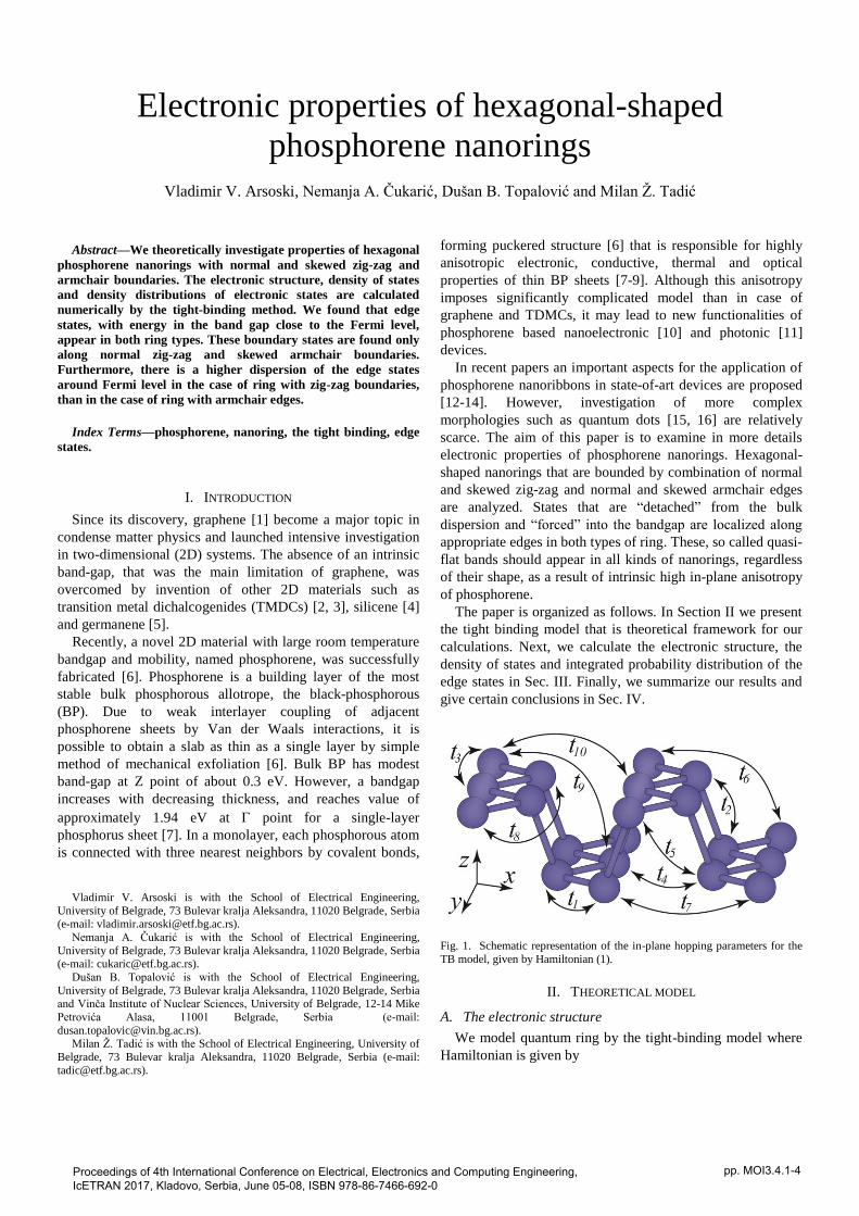
Fig. 1. Schematic representation of the in-plane hopping parameters for the
TB model, given by Hamiltonian (1).
II. THEORETICAL MODEL
A. The electronic structure
We model quantum ring by the tight-binding model where
Hamiltonian is given by
Electronic properties of hexagonal-shaped
phosphorene nanorings
Vladimir V. Arsoski, Nemanja A. Čukarić, Dušan B. Topalović and Milan Ž. Tadić
Proceedings of 4th International Conference on Electrical, Electronics and Computing Engineering, IcETRAN 2017, Kladovo, Serbia, June 05-08, ISBN 978-86-7466-692-0
pp. MOI3.4.1-4

.
ji
jiij cctH (1)
Here the summation runs over all lattice sites of nanoring, tij is
the transfer energy between i-th and j-th sites, and )( ji cc is
the creation (annihilation) operator of electron on site i(j). It
has been shown that a simple model, described by five in-
plane parameters [17], gives correct results for devices based
on the single layer phosphorene [12, 13, 15]. For a thin sheet,
a simple quantum confinement picture in vertical direction is
satisfactory, but the bandgap is underestimated due to
oversimplified picture of inter- and intra-layer hopping links.
Here we use more complex description which employs ten in-
plane hopping parameters in the TB model that results in more
precise description of the band-gap for single-layer
phosphorene, as well as for multilayer phosphorene when
additional five inter-layer parameters are included in the
model [7]. We used Bravais lattice parameters [18] to
calculate distances for corresponding hopping links between
sites. The in-plane hopping links are schematically depicted in
Fig. 1. The transfer energies [7] and calculated hopping
lengths are explicitly given in Table I.
B. The density of states
In the above model we disregarded the finite temperature
effect. Therefore, the electronic density of states (DOS) is
obtained as a sum of the Dirac functions. In order to account
finite line width the discrete energy levels Ei are broadened to
a Gaussian-shape function. The resultant energy DOS is
i E
i
E
EEED
2
2
2
)(exp
2
1)(
, (2)
where the Gaussian real mean square (RMS) width is denoted
by E.
TABLE I
SUMMARY OVERVIEW OF THE TRANSFER ENERGIES (IN EV) AND CALCULATED
DISTANCES (IN Å) FOR CORRESPONDING HOPPING BETWEEN LATTICE SITES IN
TERMS OF THE TB HAMILTONIAN. THE HOPPING LINKS ARE SCHEMATICALLY
DEPICTED IN FIG. 1.
h th [eV] dh [Å]
1 –1.486 2.2236
2 +3.729 2.2444
3 –0.252 3.3136
4 –0.071 3.3341
5 +0.019 3.4747
6 +0.186 4.2448
7 –0.063 4.3763
8 +0.101 5.1869
9 –0.042 5.3850
10 +0.073 5.4893
C. The electronic density distribution
The eigenvectors, that are output from the TB model, are
weights of the on-site localization. To obtain more realistic
real space distribution we use the square of the weight
coefficients ui which is smoothed by Gaussian blur which has
standard deviation r. This way, we obtain the electronic
density distribution
i r
i
r
iuyx
2
222
2
)(exp
2),(
rr. (3)
Here ri is the vector containing coordinates of the i-th atomic
site and r is the real space position vector.
Fig. 2. (a) The eigen-energies of HEX-ZZ ring with Nout=12 and Nin=6 and
(b) corresponding energy density of states. (c) The overall electronic density
distribution of the edge states.
III. NUMERICAL RESULTS AND DISCUSSION
We analyze hexagonal-shaped nanorings with both, zig-zag
and armchair boundaries. Our aim is to compare results for
rings with different type of boundaries but of the same size.

This can’t be exactly achieved, since phosphorene has high in-
plane structural anisotropy. Therefore, we analyze rings with
similar widths and sizes. The size of the outer ring boundary
is defined by the number of hexagonal plaquets Nout along
each side of hexangular contour which encircles the ring. The
inner size Nin is determined by the size of the hexagon that is
removed from the interior in order to make ring. We account
finite line width by spreading each eigenstate to Gaussian
form with the standard deviation E = 50/ 2 meV. To better
visualize the real space distribution of the edge states we plot
the sum of electronic densities of all in-gap states. We use the
standard Gaussian blur r =dsr/3.42, where dsr=(d1+d2)/2 is the
average length of the covalent bonds.
Fig. 3. (a) The eigen-energies of HEX-AC ring with Nout=8 and Nin=4, and
(b) corresponding energy density of states. (c) The overall electronic density
distribution of the edge states.
In Fig 2.(a) we show the electronic structure in hexagonal-
shaped ring enclosed with normal and skewed zig-zag
boundaries denoted by HEX-ZZ. Due to structural symmetry
of the ring all electronic states are double degenerated. This
symmetry may be broken by external magnetic or in-plane
electric field. Along the eigenvalues, we display the
corresponding energy DOS. Note that there is a wide
dispersion of the in-gap states and some of them almost reach
the bottom of the conduction band. Calculated value for the
band gap is 2.172eV. This is somewhat higher than the value
for the infinite phosphorene sheet, which is an effect of lateral
confinement in such a small nanostructure. Next, we show the
overall electronic density distribution of the in-gap states in
Fig. 2(c). We note that normal and skewed zig-zag edges
alternate along the ring boundary. The localization of edge
states is along normal zig-zag boundaries, while there are no
edge states along skewed zig-zag boundaries. Similar
localization of states is found in phosphorene nanoribbons
with the same type of edges [14]. Bearing in mind that the
hexagonal ring consists of “connected ribbons”, localization
follows the expected behavior.
Next, we show the energies and DOS in hexagonal-shaped
ring with normal and skewed armchair boundaries (HEX-AC)
in Fig. 3(a) and (b), respectively. All states are double
degenerated due to symmetry. Unlike the HEX-ZZ rings, the
edge states are piled around the Fermi level away from the
conduction and the valence band. The value of the band gap is
2.2 eV, which is close to the value for the HEX-ZZ ring. As
found for phosphorene nanoribbons [14], the in-gap states
exist only along skewed armchair boundaries. We note that
states on the upper and the lower boundary are separated with
relatively long ribbons. However, these vertically positioned
ribbons don’t support in-gap states. Therefore, it will be
difficult to connect these boundaries in terms of the electronic
transport.
IV. CONCLUSION
The electronic structure of hexangular phosphorene
nanorings has been theoretically investigated by means of the
tight-binding model. All states are double degenerated
because of rings symmetry. We found that edge states appear
in both types of rings. These states are found along normal
zig-zag and skewed armchair boundaries. Due to large
anisotropy, edge states may appear on various types of
boundaries. Apart from hexagonal-shaped phosphorene
nanorings, these states should appear in all other structures
regardless on a shape. There is a relatively small energy
difference between the in-gap states. However, the states that
reside on the upper boundaries are physically separated from
the states with similar localization on the lower boundary.
Namely, the upper and the lower part of both type of ring are
connected with either normal armchair or skewed zig-zag
ribbons. Therefore, topological effects related to the
application of perpendicular magnetic field will be very hard
to attain. Investigation of electronic structure in the presence
of a magnetic field will be the subject of our future research.

ACKNOWLEDGMENT
This work was supported by the Serbian Ministry of
Education, Science and Technological Development No.
III45003. The authors would like to thank Dr. Marko Grujić
research associate at School of Electrical Engineering for
useful discussions regarding phosphorene nanodots.
REFERENCES
[1] K.S. Novoselov, A. K. Geim, S. V. Morozov, D. Jiang, Y. Zhang, S. V. Dubons, I. G. Grigorieva, and A. A. Firsov, “Electric Field Effect in
Atomically Thin Carbon Films,” Science, vol. 306., pp. 666-669, Oct.,
2004. [2] D. Xiao, G.-Bin Liu, W. Feng, X. Xu, and W. Yao, “Spin and Valley
Physics in Monolayers of MoS2 and Other Group-VI Dichalcogenides,”
Phys. Rev. Lett., vol. 108, no. 19, pp. 196802/1-5, May, 2012. [3] B. Radisavljević, A. Radenović, J. Brivio, V. Giacometti, A. Kis,
"Single-Layer MoS2 Transistors", Nat. Nanotechnol., vol. 6, pp. 147-
150, Feb., 2011. [4] P. Vogt, P. De Padova, C. Quaresima, J. Avila, E. Frantzeskakis, M. C.
Asensio, A. Resta, B. Ealet, and G. L. Lay, “Silicene: Compelling
Experimental Evidence for Graphenelike Two-Dimensional Silicon,” Phys. Rev. Lett., vol. 108, no. 15, pp. 155501/1-5, Apr., 2012.
[5] E. Bianco, S. Butler, S. Jiang, O. D. Restrepo, W. Windl, J. E.
Goldberger, “Stability and exfoliation of germanene: a germanium graphane analogue,” ACS Nano, vol. 7, no. 5, pp. 4414-4421, Mar.,
2013. [6] H. Liu, A. T. Neal, Z. Zhu, Z. Luo, X. Xu, D. Tománek, and P. D. Ye,
“Phosphorene: An Unexplored 2D Semiconductor with a High Hole
Mobility,” ACS Nano, vol. 8, no. 4, pp. 4033-4041, Mar., 2014. [7] A. N. Rudenko, S. Yuan, and M. I. Katsnelson, “Toward a realistic
description of multilayer black phosphorus: From GW approximation to
large-scale tight-binding simulations,” Phys. Rev. B, vol. 92, no. 8, pp.
085419/1-9, July, 2015; See Erratum: A. N. Rudenko, S. Yuan, and M.
I. Katsnelson, Phys. Rev. B, vol. 93, no. 19, pp. 199906, May, 2016. [8] A. Jain and A. J. H. McGaughey, “Strongly anisotropic in-plane thermal
transport in single-layer black phosphorene,” Sci. Rep., vol. 5, pp.
08501/1-5, Feb., 2015. [9] V. Tran, R. Soklaski, Y. Liang, and L. Yang, “Layer-controlled band
gap and anisotropic excitons in few-layer black phosphorus,” Phys. Rev.
B, vol. 89, no. 23, pp. 235319/1-6, Jun., 2014. [10] L. Li, Y. Yu, G. J. Ye, Q. Ge, X. Ou, H. Wu, D. Feng, X. H. Chen,
and Y. Zhang, “Black phosphorus field-effect transistors,” Nat.
Nanotechnol., vol. 9, pp. 372-377, May, 2014. [11] J. Dai and X. C. Zeng, “Bilayer Phosphorene: Effect of Stacking Order
on Bandgap and Its Potential Applications in Thin-Film Solar Cells,” J.
Phys. Chem. Lett., vol. 5, pp. 1289-1293, May, 2014. [12] M. Ezawa, “Topological origin of quasi-flat edge band in phosphorene,”
New J. Phys., vol. 16, no. 11, pp. 115004/1-13, Oct., 2014.
[13] E. T. Sisakht, M. H. Zare, and F. Fazileh, “Scaling laws of band gaps of
phosphorene nanoribbons: A tight-binding calculation,” Phys. Rev. B,
vol. 91, no. 8, pp. 085409/1-085409/8, Feb., 2015.
[14] M. M. Grujić, M. Ezawa, M. Ž. Tadić, and F. M. Peeters, “Tunable skewed edges in puckered structures,” Phys. Rev. B, vol. 93, no. 24, pp.
245413/1-7, Jun., 2016.
[15] R. Zhang, X. Y. Zhou, D. Zhang, W. K. Lou, F. Zhai, and K. Chang, “Electronic and magneto-optical properties of monolayer phosphorene
quantum dots,” 2D Mat., vol. 2, no. 5, pp. 045012/1-7, Nov., 2015.
[16] X. Zhang, H. Xie, Z. Liu, C. Tan, Z. Luo, H. Li, J. Lin, L. Sun, W. Chen, Z. Xu, L. Xie, W. Huang, and H. Zhang, “Black Phosphorus
Quantum Dots,” vol. 54, no. 12, pp. 3653-3657, Mar., 2015.
[17] A. N. Rudenko and M. I. Katsnelson, “Quasiparticle band structure and tight-binding model for single- and bilayer black phosphorus,” Phys.
Rev. B, vol. 89, no. 20, pp. 201408(R)/1-5, May, 2014.
[18] W. M. Haynes Eds., “Properties of Solids,” in CRC Handbook of Chemistry and Physics, 95th ed., Boca Raton, Florida, USA: CRC Book
Taylor & Francis Group LCC, 2014, ch. 12, pp. 12-17.