electronic structure and catalytic properties · pdf fileelectronic structure and catalytic...
TRANSCRIPT
A. I. Kulak, E. A. Streltsov,D. V. Sviridov
ELECTRONIC STRUCTURE AND CATALYTIC PROPERTIESOF OXIDE SEMICONDUCTORS MODIFIED WITH FINE METAL
PARTICLES
INTRODUCTION
Catalysis of redox reactions is an important goal in photochemistry and
photocatalysis because even small overvoltages diminish the efficiency of such
systems immensely. Deposition of different metals (e.g., Pt, Ag, Pd) has often
been employed to enhance the activity of semiconductor photocatalysts. Thus, the
modification of semiconductor particles with the noble metals acting as a sink of
photoinduced charge carriers and promoting interfacial charge-transfer proce-
sses, appears to be an essential factor for maximizing the efficiency of photocata-
litic water splitting reactions as well as the processes of the photoinduced degra-
dation of toxic organics. The deposition of metal particles possessing electrocata-
lytic activity also permits to realize photosynthetic reaction which are hardly fea-
sible with the use of naked semiconductor photocatalyst. The enhancement of the
performance of the photoelectrochemical cells as the result of modification of the
photoelectrode surface with metal islets results not only from the mere elevation
of electrocatalytic activity of the electrode surface but also from the suppression
of the recombination due to changes in the structure of electronic states in a for-
bidden zone of the semiconductor produced by strongly adsorbing ad-atoms and
metal clusters.
Notwithstanding to the fact that the modification of semiconductors with me-
tal particles is widely used to improve the performance of different photocataly-
tic, photoelectrochemical and electrochemical systems, the interaction between
metal nanoparticles and semiconductor support as well as an exact mechanism of
operation of metal-loaded catalysts is not yet clearly understood. Thus, for exam-
ple, still controversial remain: the exact role of electroactive (interfacial) states
and Schottky barriers at the semiconductor/metal nanocontacts; the origin of the
size dependence of catalytic activity of metal particles; the effect of the depositi-
on conditions on the modifying activity of metal nanoparticles. To clarify these is-
sues, the investigations rewired in this paper were carried out using well-identifi-
ed thin-film oxide electrodes (mainly TiO2 as a model photoelectrodic material)
modified with metal nanoparticles which were applied onto the semiconductor
surface by different deposition techniques.
CHEMICAL PROBLEMS OF THE DEVELOPMENT OF NEW MATERIALS AND TECHNOLOGIES
Minsk 2003
1. CHARACTERISTIC FEATURES OF OXIDE SEMICONDUCTORSAS THE ELECTRODE MATERIAL
The donor centers in the wide-bandgap heavily doped oxide semiconductors,
such as amorphous and polycrystalline titanium dioxide, exhibit strong tendency
to form associates. Depending on the semiconductor pre-history and doping level,
the donor associates may have different sizes (from few nanometers to tens micro-meters, representing, in the latter case, the microphase inclusions such as Magne-li phases or Ti2O3). At sufficiently high concentrations of donor associates, they
can overlap forming the percolation cluster which may act as an additional chan-nels ensuring charge transfer through the semiconductor bulk to the electrode
surface with the much higher efficiency as compared with the charge transfer via
the semiconductor bands [1–3]. Such percolation clusters, exhibiting the properti-es of degenerated semiconductor or even metal, are characterized by hopping or
metal-like conductivity and do not form Schottky barriers both at grain boundari-es and in contact with electrolyte. On the other hand, when the donor clusters are
sufficiently large to be considered as the microphase inclusions, it is inconceivable
that the potential barriers may appear at the interfaces between the donor clus-
ters and semiconductor matrix in which they are formed. In this case, the charge
flows through the semiconductor bands and through the percolation cluster are to
be completely independent. The donor clusters at the surface of semiconductor
oxide electrode can be observed directly employing specially developed versions of
photoelectrochemical microscopy (by measuring a local cathodic current at negati-
ve biases [4–5] or detecting the higher harmonics of the electrode ac-photorespon-
se to the periodic laser pulses which have been shown to be directly proportional
to the donor density [6, 8]).
In terms of energetic diagram, the segregation of donor centers inherent in
the heavily doped oxides can be described by the fluctuations of the energetic le-
vels resulting in the formation of the potential relief at the electrode surface. In
case of amorphous, amorphous-crystalline and polycrystalline TiO2 prepared by
hydrolysis of titanium alcoxides these fluctuations appears to be large enough to
make it possible almost unimpeded charge transfer in the heterojunctions «oxi-
de-oxide" (WO3/TiO2, Bi2O3-TiO2, etc.) [9, 10].
The formation of percolation cluster as the result of segregation of donor centers
plays a valuable role in the formation of the dark anodic behaviour of thin-film TiO2,
WO3, Bi2O3 electrodes [1–3]. In particular, the anodic current at the positively-bia-
sed highly-doped electrodes can be attributed to the electron transfer along percola-
tion cluster rather then to the tunneling through the space charge region. This conc-
lusion is confirmed by numerous experimental facts, including much higher values
of anodic current than the calculated tunnel current, the characteristic shape
of i, E-curves, and much higher sensitivity of dark current on the electrolyte compo-
sition than one would expect [3].
61ELECTRONIC STRUCTURE AND CATALYTIC PROPERTIESOF OXIDE SEMICONDUCTORS MODIFIED WITH FINE METAL PARTICLES
2. EFFECT OF DEPOSITION TECHNIQUE ON THE MORPHOLOGY OFMETAL NANOPHASE GROWN ON THE SEMICONDUCTOR SURFACE
2.1. Contact deposition
The immersion of chemically-active semiconductors, such as silicon, germa-nium, AIIIBV compounds in the solution containing the ions of metals (Au, Ag,
Hg, Cu, etc.) which have more positive electrochemical potential than that of a
semiconductor, leads to the formation of metal islets on the semiconductor sur-face. In this case, the surface concentration of deposited metal particles as well
as the dispersity of growing nano- (micro-) phase appear to be dependent on
numerous factors such as the concentration of metal ions in the solution, the
deposition time, the porosity of the passive layer at the surface of the semicon-ductor, as well as the chemical properties of a metal and a semiconductor in use.
On the other hand, one can also observe less evident phenomenon consisting in a
spontaneous deposition of metal nanophase under the treatment of chemically
inert semiconductors (such as titanium dioxide) with the metal ion-containing
solution in the absence of the external bias, illumination, and reducing agents.
During the contact deposition, the metal particles are formed as the result of
interaction of metal ions with donor defects or donor associates in the semicon-
ductor. In principle, this process may proceed both through the direct chemical
reaction of donor centers with metal ions and via so-called electrochemical mec-
62 A. I. Kulak, E. A. Streltsov,D. V. Sviridov
0 8 10
1
2
0
1
2 a
c
91
2 4 6 1 2 3
d, nm d, nm
0
2
4
b
Nd = 10 cm18 –3Nd = 10 cm
19 –3
Nd = 10 cm19 –3
Nd = 10 cm18 –3
t = 1 mint = 1 min
t = 10 min t = 10 min
0 1 2 3 4
2
d
N10
,cm
p×
–10
–2
N10
,cm
p×
–9
–2
Fig. 1. Size distribution of Ag particles grown on thin TiO2 film.
The particles were deposited by treating TiO2 electrode with 0.001 M Ag2SO4.
hanism involving a spatial separation of the reactions of oxidation of donor cen-ters and growing of metal particles. With titanium dioxide and, probably, with
many other oxide semiconductors, the electrochemical mechanism of sponta-neous deposition of metal nanophase seems to be more credible than a pure che-mical one. This is evidenced by the fact that the resulted metal particles have
relatively large sizes and are positioned at the intervals much more (16–40 ti-mes) than the particle diameter [1,3]. Thus, during immersion of TiO2 electro-
de, characterized by the concentration of ionized donors (Nd) of 1019 cm–3, into
10–5–10–3 M Ag+-containing aqueous solutions, the average size of Ag nuclei in-
creases from 0.8–0.9 to 9–10 nm as the time during which the electrode is im-mersed into solution increase from 1 to 10 min. Under the same conditions, the
average size of Ag particles in the case of TiO2 electrode with Nd = 1018 cm–3 ri-ses from 0.7 to 3.2 nm (Fig. 1). Under more prolonged exposure of TiO2 electro-des to the Ag+-containing solutions, the size of the particles as well as their sur-face concentration rise moderately. It is characteristic that, in both cases, only
a small portion of the electrode surface appears to be covered with silver (no
more than 2–6 % in the case of TiO2 electrode with Nd = 1019 cm–3).
The amount of deposited silver (in atoms/cm2) on the surface of TiO2 elect-
rode can be readily determined by measuring the current passing during anodic
oxidation of Ag particles at a linear potential sweep. At rather high concentra-
tions of donor centers in the initial titanium dioxide (Nd ∼ 1019cm–3), a detectab-
le background current is observed on the potentiodynamic i, E-curves obtained
with these electrodes in indifferent electrolytes in the absence of redox additi-
ves, this current being attributed to the oxidation of donor centers in a semi-
conductor. After the treatment of the electrode with the Ag+ ions, the backgro-
und current dies out almost completely and, in its instead, the well-pronounced
peak corresponding to the anodic oxidation of Ag particles appears (Fig. 2). The
diminishing of the background current is associated with the consumption of
donors in the reaction with Ag+ ions as well as with the re-distribution of the
potential drop from the free (uncovered) TiO2 surface to the surface of Ag part-
icles. High chemical reactivity of metal nanophase and a large surface-to-volu-
me ratio for the deposited nanoparticles hinder the passivation processes, and a
complete oxidation of Ag particles with the average size of 1–3 nm occurs at pH
5–7 even in the absence of depassivators. It should be noted that, when employ-
ing conventional potentiostatic setup for the determination of the surface con-
centration of Ag particles, the sensitivity of this method is no worse than 1013
atoms/cm2, i.e. about 0.01 of monolayer coating. Taking into account that the
average size of Ag particles deposited by this technique lies in the range from 1
to 10 nm, one can estimate from the peak of anodic current on the potentiodyna-
mic i,E-curves that the surface concentration of nanoparticles to be of 109–1012
cm–2. It should be borne in mind that, when the average size of Ag particles ex-
ceeds 4–5 nm, the above method becomes less accurate because of the appearan-
ce of the passivation processes. The effect of these processes can be diminished
by the introduction of depassivating additives (halide, rhodanate, and sulfide
ions) into electrolyte (Fig. 2) provided that particular precautions (very careful
removal of dissolved oxygen, etc.) are taken in order to prevent the loss of the
chemically unstable smallest-sized fraction.
63ELECTRONIC STRUCTURE AND CATALYTIC PROPERTIESOF OXIDE SEMICONDUCTORS MODIFIED WITH FINE METAL PARTICLES

Table 1Surface concentration (Np), the ranges of particles Pd sizes (d)
and average sizes of Pd particles (da) for TiO2-Pd films synthesized
by combined pyrolysis of palladium chloride and titanium resinate (RTi)
on air at 450 oC (1 h) and then annealed in hydrogen at 500 îC and 800 îÑ
for 1 h, by vacuum deposition of Pd and by adsorption
of Pd2+ ions on TiO2 film obtained by pyrolysis of titanium resinate
Method of preparation
of TiO2-Pd film
500 îÑ 800 îÑ
d, nm da, nm Np, cm-2 D, nm da, nm Np, cm-2
Combined pyrolysis of PdCl2and RTi
2–6 4.5 8.6 × 10¹⁰ 2–15 8 1.2 × 10¹¹
Vacuum deposition of Pd 2–20 9 3.3 × 10¹¹ 2–50 14 1.0 × 10¹¹
Adsorption of Pd2+ ions on
TiO2 film2–120 17 4.4 × 10¹⁰ 4–160 36 2.0 × 10¹⁰
Using this approach, we have examined [11] the properties and concentration
of electroactive (i.e., which are able to take part in the electrode processes) Pd na-
noparticles formed by different methods: (i) combined pyrolysis of palladium
64 A. I. Kulak, E. A. Streltsov,D. V. Sviridov
0.2 0.4 0.6 0.8
0
2
4
6
8
10
43
2
1
Electrode potential,V (vs. Ag|AgCl)
Current
densi
ty,
A·c
mμ
–2
Fig. 2. Potentiodynamic current-potential curves of oxidation of silver
particles deposited on thin-film TiO2 electrode. The curves have been obtained
in deaerated 0.1 M KCSN + 0.5 M K2SO4 solution (curve 1),
0.1 M K4Fe(CN)6 + 0.5 M K2SO4 (curve 2), 0.5 M KOH (curve 3),
and 0.5 M K2SO4 (curve 4). The potential sweep rate is 40 mV/s.
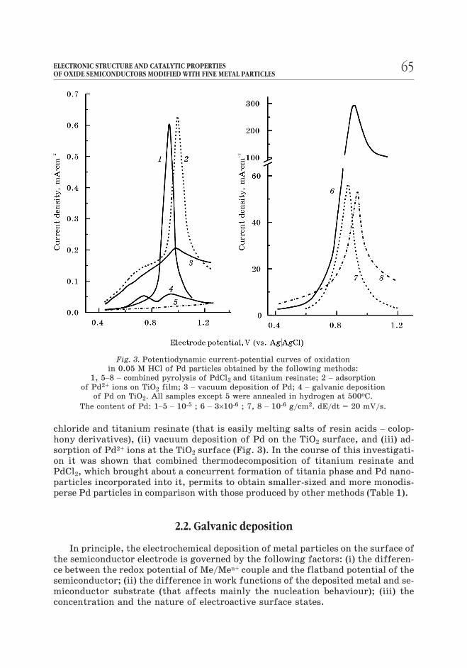
chloride and titanium resinate (that is easily melting salts of resin acids – colop-
hony derivatives), (ii) vacuum deposition of Pd on the TiO2 surface, and (iii) ad-
sorption of Pd2+ ions at the TiO2 surface (Fig. 3). In the course of this investigati-
on it was shown that combined thermodecomposition of titanium resinate and
PdCl2, which brought about a concurrent formation of titania phase and Pd nano-
particles incorporated into it, permits to obtain smaller-sized and more monodis-
perse Pd particles in comparison with those produced by other methods (Table 1).
2.2. Galvanic deposition
In principle, the electrochemical deposition of metal particles on the surface of
the semiconductor electrode is governed by the following factors: (i) the differen-
ce between the redox potential of Me/Men+ couple and the flatband potential of the
semiconductor; (ii) the difference in work functions of the deposited metal and se-
miconductor substrate (that affects mainly the nucleation behaviour); (iii) the
concentration and the nature of electroactive surface states.
65ELECTRONIC STRUCTURE AND CATALYTIC PROPERTIESOF OXIDE SEMICONDUCTORS MODIFIED WITH FINE METAL PARTICLES
Fig. 3. Potentiodynamic current-potential curves of oxidation
in 0.05 M HCl of Pd particles obtained by the following methods:
1, 5–8 – combined pyrolysis of PdCl2 and titanium resinate; 2 – adsorption
of Pd2+ ions on TiO2 film; 3 – vacuum deposition of Pd; 4 – galvanic deposition
of Pd on TiO2. All samples except 5 were annealed in hydrogen at 500îC.
The content of Pd: 1–5 – 10-5 ; 6 – 3×10⁻⁶ ; 7, 8 – 10-6 g/cm2. dE/dt = 20 mV/s.
Our investigations on the electrochemical behavior of thin-film titanium dio-xide electrodes have shown that, with cathodically biased TiO2 electrodes being in
a contact with the solutions containing such metal ions as Ag, Pt, Pd, even a
slight negative shift of the electrode potential from its stationary value causes the
growth of metal nanoparticles. During this process, the growth of the particles al-ready existing at the electrode surface predominantly occurs currently available
particles takes place, and the appearance of fresh species can be stimulated by the
increase of the applied bias. At the deposition of Ag, Cu, Pd, Pt on the TiO2 elect-rodes under the potentiostatic conditions, the increase of cathodic current with
time is observed, the current-time dependencies being often linear in a wide range
of potentials and currents. This linearity results from the combination of two fac-tors: (i) the decay of nucleation efficiency with time and (ii) the diffusion-limited
growth of the existing nuclei [1,12]. The TEM investigations has evidenced that
the time dependence of the nucleation rate, í (τ), can be approximated by the follo-wing relation (Fig. 4):
ν ττ
τατ α( )
( );
/= = =−dN
d1 2
const
Taking into account that under the diffusion control the current at a single
hemispherical metal particle is governed by
i c D k k c= = =ρ τ τ1 2 3 2 1 2 1 2/ / / /; , const
(where D is the diffusion coefficient, τ is a time elapsing from the moment of ap-
pearance of metal nucleus, ρ is the density of metal phase, k and ñ are the cons-
tants), after t minutes, the current, I, measured at an array of the growing silver
microelectrodes on the semiconductor surface amounts:
I k t d kat dt
d
t
= − = −− −
→→∫ν τ τ τ τ τ τ τ
δδ
( )( )/ / / /1 2 1 2 1 2 1 2
00
1
2
tt
kat∫∫⎛
⎝⎜⎜
⎞
⎠⎟⎟ =
→
5
30δ
.
Such current-time dependencies determine the peculiar type of potentiodyna-
mic polarization i,E-curves, the characteristic feature of which is that the cur-
rents at the reverse potential sweep are essentially higher than those observed at
the direct sweep, the effect of the potential sweep rate on the cathodic current be-
ing unusually strong (Fig. 4). Obviously, it is impossible to obtain the stationary
potentiostatic i, E-curves because a progressive linear increase of cathodic cur-
rent with time is observed the metal deposition onset potential is reached and the
quasi-stationary current could be attained only after the complete covering of se-
miconductor surface with a metal layer. Characteristic of this process is practical-
ly unimpeded electron exchange between the metal particles growing under catho-
dic bias and the semiconductor c-band as evidenced by very small value of cathodic
overvoltage (approximately the same as for the metal electrodes). This is not an
ordinary fact because the process of metal deposition occurs at the electrode po-
tentials (0.43 – 0.20 V), which are substantially higher than the flatband potential
of TiO2 (-0.4 – -0.6 V); therefore, the deposition of metals proceeds under conditi-
ons where rather high (0.6 – 0.8 V) Schottky barrier arises at the TiO2/electrolyte
66 A. I. Kulak, E. A. Streltsov,D. V. Sviridov

67ELECTRONIC STRUCTURE AND CATALYTIC PROPERTIESOF OXIDE SEMICONDUCTORS MODIFIED WITH FINE METAL PARTICLES
0 2 4 6 8 100
2
4
6
80.2 0.4
–300
–200
–100
0
0 30 60 90100
200
300
400
τ1/2 1/2, s
0 20 40 60 80
0
30
60
90
120
150
b
a
c
Electrode potential,
V (vs. Ag|AgCl)
x 10
4
3
2
1
Time,min
d
dE/dt,mV/s
N10
,cm
p×
–10
–2
Current,
A/cm
μ2
Cath
odic
current,
A/cm
μ2
Cath
odic
current,
A/cm
μ2
Fig. 4. Cathodic deposition of silver particles onto titanium-dioxide electrodes:
a) time dependence of the surface concentration of silver particles in the potentiostatic
conditions at +0.4 V (vs. sat. Ag|AgCl); b) typical view of cyclic polarization curve
obtained under cathodic deposition of silver; c) current-time dependences
for rotating disk TiO2 electrodes with Nd ≈ 1019 cm–3 (curves 1, 3, 4) and 1018 cm–3 (curve 2);
rotation speed was 900 (curve 1), 300 (curve 2, 3) and 180 rpm (curve 4);
d) typical current vs. electrode potential sweep rate curve.
junction. The existence of a distinct Schottky barrier on the surface of TiO2 elect-rode free of the metal particles is confirmed by the impedance measurements (the
linear Mott-Schottky plots [3]) and by the high photovoltage (Voc = 0.5 – 0.6 V)
2.3. Photoinduced (photocatalytic) deposition
The photocatalytic deposition of metal from contacting solutions can be usedfor the removing of metal ions (especially, the toxic ones, such as Hg2+, Pb2+,Cd2+, Cr3+ and for the improving the activity of semiconductor photocatalysts andphotoelectrodes [1,3,13]. The photoselective version of this process has been in-vestigated for the potential application in the fabrication of microelectronic cir-cuits and devices [2,3] and for the development of novel silver-halide and non-sil-ver imaging systems [2,3,14,15]. A specialcase of the formation of metalnanophase under illumination is a direct photolysis of the semiconductor matrixthat is inherent, e.g., for bismuth oxihalides [16–18].
The mechanism and kinetics of the process of nucleation of small metal parti-cles on the semiconductor surface have been studied with the use of silver ionphotoreduction on the titania surface as a model reaction [2,3]. In these re-searches the consideration has been given to the photogeneration of the elec-tron-hole pairs in titanium dioxide with subsequent interaction of photogeneratedholes with adsorbed water molecules, OH- ions, or hole-accepting species and trap-ping of the electrons with the surface states followed by the reduction of Ag+ ions.In the presence of Ag+ ions, the charge exchange between Ag particles on the elec-trode surface and Ag+ ions in the solution appears to be very efficient so that theaction of UV irradiation under the open circuit conditions causes only a slightnegative shift of the electrode potential (Fig. 5).
This shift corresponds to the establishment of the equilibrium between twohalf-reactions involved in the photocatalytic process. The first half-reaction is the re-duction of silver on the semiconductor surface (the cathodic partial process in whichthe majority charge carriers are involved), while the second one is the conjugated ano-dic partial process related to the generation and consumption of photoholes. Under il-lumination of the electrode, the parameters of the electronic surface states may exhi-bit a slight change; moreover, in the case of the lightly-doped semiconductors, the in-tense illumination may offer a substantial increase of the concentration of majoritycharge carriers. Hence some differences may exist between the kinetic characteristicsof the dark reaction of metal ion reduction and the cathodic half-reaction involved inthe overall photocatalytic process in spite of the participation of majority charge car-riers in the both processes. Nevertheless, according to our experimental results [1,3],the effect of the illumination on the parameters of the cathodic half-reaction is actual-ly insignificant in many cases including the reaction of the photocatalytic depositionof Cu and noble metals onto the surface of titanium dioxide and other wide-bandgapsemiconductors. Taking this into account, the dark cathodic part of the net polarizati-on curve can be reasonably used for simulation of the reductive half-reaction involvedin the overall photocatalytic process.
The above features of the cathodic growth of metal particles on the surface ofsemiconductor TiO2 electrode surface are best consistent with the behavior of tita-nium dioxide characterized by the moderate concentrations of ionized donors
(Nd ≈ 1018 cm–3). In this case, the electrochemical and photocatalytic behaviour of
68 A. I. Kulak, E. A. Streltsov,D. V. Sviridov

the TiO2 electrode modified by the metal nanoparticles can be simulated by theequivalent circuit consisting of two parallel-connected independent parts: a set ofmetal nanoelectrodes, on the one hand, and a semiconductor surface free of metalparticles, on the other hand.
69ELECTRONIC STRUCTURE AND CATALYTIC PROPERTIESOF OXIDE SEMICONDUCTORS MODIFIED WITH FINE METAL PARTICLES
EC
EF
EV
+
+
-
-
EC
EF
EV +
-
0.0 0.5 1.0 1.5 2.0 2.5 3.0 3.5 4.0 4.5
–0.8
–0.6
–0.4
–0.2
0.0
0.2
0.4
0.6
4
3
2
1
off
off
on
on
Time,min
Ele
ctr
ode
pote
nti
al,
V(v
s.A
gA
gCl)
⏐
onoff c
a b
Ag/Ag+
Ag/Ag+
Fig. 5. Energy diagrams of TiO2 in contact with the electrolyte
containing Ag+ ions under open circuit conditions in the dark
(solid lines) and under illuminations (dashed line):
a – moderately doped TiO2 (Nd ~ 1016– 1018 cm–3 );
b – heavily doped TiO2 (Nd ~ (1–5)×1019 cm–3);
c – Time dependence of TiO2 electrode potential under UV illumination
in 0.2 M K2SO4: without additives (curves 2, 3), in presence
of 0.05 M Ag+ (curves 1, 4). Concentration of ionized donors
in TiO2 was 1019 cm–3 (curves 1, 2) and 5 × 1017 cm–3 (curves 3, 4)

With substantially decreased doping of titanium dioxide(up to Nd = 1016–
1017 cm–3), the deposited Ag particles offer the essentially less values of the ex-change current in contact with the electrolyte contained Ag+ ions as well as the
less surface concentration of the metal nanophase (calculated in atoms/cm–2). As
the result, the effect of metal nanoparticles is reduced mainly to the modification
of the structure of existing electronic surface states rather than to the introducti-on of new ones that, in particular, enables high open-circuit photovoltage to be ge-nerated under UV illumination (Fig. 5). For such electrode, we should also intro-duce into the equivalent electric circuit an additional resistance or «diode» ele-ment that mimic the metal-semiconductor junction, as well as an impedance ele-ment corresponding to the electronic surface states on the free semiconductor sur-face and that covered by metal nanoparticles.
We have established that for more refined understanding of the process of Ag
deposition onto TiO2 it is necessary also to take into account the role of the elect-ronic surface states induced by the chemisorbed Ag+ ions and growing Ag nanoc-lusters, the characteristic features of the interaction of silver ions and particles
with donor defects and their associates in the oxide, the changes in the structure
of a double electric layer localized at the sites of metal particle deposition, the va-
riations of the electrode electrocatalytic properties originated from the appearan-
ce of nano- and microphase, etc. [2, 3, 19–21].
The difference in the modification action of metal islets of comparable sizes
deposited by different methods can be attributed to the fluctuations of energy le-
vels arising as the result of the inhomogeneity of the semiconductor surface. Due
to this, the metal particles deposited by photocatlytic and electrochemical met-
hods align themselves on distinct areas of the semiconductor surface which differ
as to the Nd and corresponds to the different portions of potential relief. Thus, the
cathodic deposition occurs in the most pronounced minima in this relief (which
are the most likely corresponding to the donor associates), while the photocataly-
tic deposition is induced by photoelectrons generated under illumination at the
moderately doped areas on the semiconductor surface, these nonequlibrium elect-
rons then flowing downslope to the nearest minimum where the reduction of me-
70 A. I. Kulak, E. A. Streltsov,D. V. Sviridov
+
-
2 2 2
h Eν ≥ g
2
2
11
EC
EF
EV
Eg’
E g
EC
EF
EV
E
x
ab
Fig. 6. Macrofluctuations of the energy levels at the semiconductor surface:
(a) of the covariant type; (b) of the contravariant type (b).The arrows show the places where the electrochemical (1) and photocatalytic (2)
reduction of metal ions occurs

tal ions takes place. The potential fluctuations thus facilitate the lateral separati-on of photogenerated charges, the electron and hole reactions being localized at
the separate at the illuminated semiconductor surface. Alongside with the charge
separation events, some flattening of the potential relief occurs under illuminati-on (in similar manner to the photoinduced band unbending under open circuit con-ditions). As the result, a number of places at the electrode surface which have the
potential negative enough to induce the reduction of metal ions increases. This
provide an explanation of the fact that the photocatalytically-deposited metal ap-pears to be much more dispersed as compared to the galvanic deposit; by the same
token the increase of the light intensity, which should ensure the further flatte-ning of the surface potential relief, results in the increase of concentration of Ag
nuclei.
3. ELECTRONIC SURFACE STATES IN THE FORBIDDEN ZONEOF SEMICONDUCTOR INDUCED AS A RESULT OF DEPOSITION
OF METAL PARTICLES ON SEMICONDUCTOR SURFACE
Electrolyte electroreflectance (EER) spectroscopy is a powerful tool for the in
situ investigation of band structure of semiconductor electrodes contacting with
the electrolyte solution. In the EER experiments, a periodically modulated elect-
ric field is applied to the semiconductor electrode, which causes small changes in
the reflectivity and the absorbance. When the modulated electric field is suffici-
ently low, the lineshape of the EER spectrum of non-degenerate semiconductor is
determined by the modulation-induced effect of population-depopulation of the
electronic surface states (in the sub-bandgap absorption range) or is closely rela-
ted to the third derivative of the dielectric function (in the bandgap absorption
range). This spectroscopic technique has sown a promise in determining the poten-
tial distribution inside the nanocrystalline films and between the space charge and
Helmholtz (or surface oxide) layer, studying the evolution of space charge region
in the degenerated semiconductors contacting with the electrolyte solution, mea-
suring the flatband potentials, and obtaining information on the degree of inho-
mogeneity of electrode surface. High sensitivity of EER technique (it is possible
to detect the ÄR/R values of about 10–5–10–7) permits to detect not only the bulk
electronic levels but also to evaluate the concentration and energy distribution of
energy states at the surface of naked and metal-modified semiconductor in con-
tact with aqueous solution [1–3,19–27].
It is seen from Fig. 7 that in case of amorphous TiO2 film only the bandgap
transitions contribute to a EER spectrum which appears to be closely similar to
that of single crystalline oxide. The analogous EER spectra observed for amorp-
hous and monocrystalline TiO2 point to the fact that in both cases the semiconduc-
tor surface is almost clean from energy states capable of contributing to EER res-
ponse. The annealing of amorphous TiO2 films accompanied with the formation of
crystalline phase, gives rise to an intense EER signal peaking in the sub-bandgap
region (Fig. 7). This sub-bandgap EER response can be attributed to the localized
electronic states (presumable not only pure surface states but also those residing
in grain boundaries as well). The electroactive states created upon crystallisation
71ELECTRONIC STRUCTURE AND CATALYTIC PROPERTIESOF OXIDE SEMICONDUCTORS MODIFIED WITH FINE METAL PARTICLES
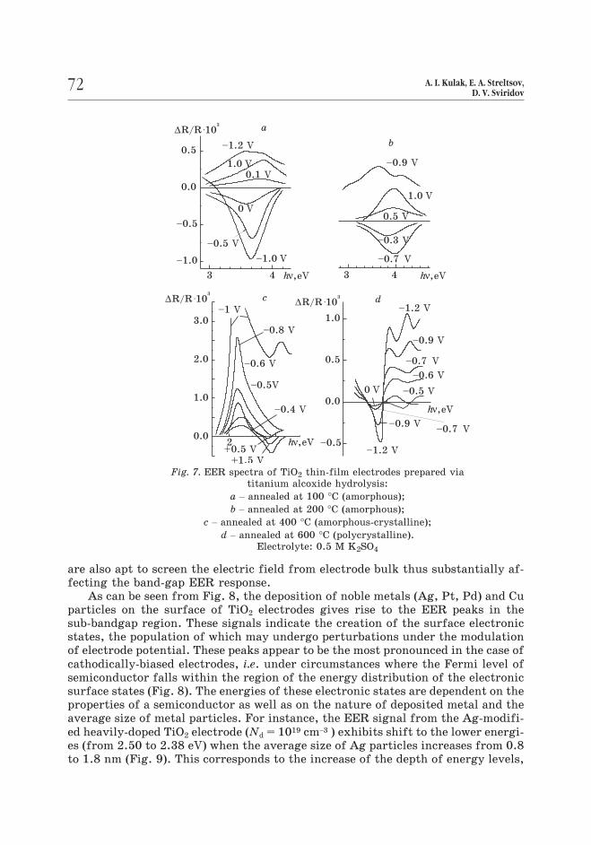
are also apt to screen the electric field from electrode bulk thus substantially af-
fecting the band-gap EER response.
As can be seen from Fig. 8, the deposition of noble metals (Ag, Pt, Pd) and Cu
particles on the surface of TiO2 electrodes gives rise to the EER peaks in the
sub-bandgap region. These signals indicate the creation of the surface electronic
states, the population of which may undergo perturbations under the modulation
of electrode potential. These peaks appear to be the most pronounced in the case of
cathodically-biased electrodes, i.e. under circumstances where the Fermi level of
semiconductor falls within the region of the energy distribution of the electronic
surface states (Fig. 8). The energies of these electronic states are dependent on the
properties of a semiconductor as well as on the nature of deposited metal and the
average size of metal particles. For instance, the EER signal from the Ag-modifi-
ed heavily-doped TiO2 electrode (Nd = 1019 cm–3 ) exhibits shift to the lower energi-
es (from 2.50 to 2.38 eV) when the average size of Ag particles increases from 0.8
to 1.8 nm (Fig. 9). This corresponds to the increase of the depth of energy levels,
72 A. I. Kulak, E. A. Streltsov,D. V. Sviridov
3 4
–1.0
–0.5
0.0
0.5
hν,eV
hν,eV
hν,eVhν,eV
–1.0 V
–0.5 V
0 V
0.1 V1.0 V
–1.2 V
20.0
1.0
2.0
3.0
–0.5
0.0
0.5
1.0–1 V
–0.8 V
–0.6 V
–0.5V
+1.5 V+0.5 V
–0.4 V
–1.2 V
–0.9 V
–0.7 V
–0.6 V
–0.5 V
–1.2 V
–0.9 V–0.7 V
0 V
3
a
b
c d
4
–0.7 V
–0.3 V
0.5 V
1.0 V
–0.9 V
ΔR/R 10⋅ 3
ΔR/R 10⋅ 3
ΔR/R 10⋅ 3
Fig. 7. EER spectra of TiO2 thin-film electrodes prepared via
titanium alcoxide hydrolysis:
a – annealed at 100 °C (amorphous);
b – annealed at 200 °C (amorphous);
c – annealed at 400 °C (amorphous-crystalline);
d – annealed at 600 °C (polycrystalline).
Electrolyte: 0.5 M K2SO4
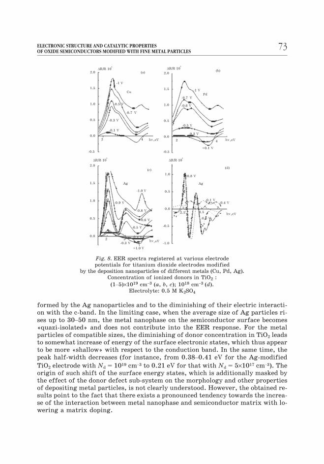
formed by the Ag nanoparticles and to the diminishing of their electric interacti-
on with the c-band. In the limiting case, when the average size of Ag particles ri-
ses up to 30–50 nm, the metal nanophase on the semiconductor surface becomes
«quazi-isolated» and does not contribute into the EER response. For the metal
particles of compatible sizes, the diminishing of donor concentration in TiO2 leads
to somewhat increase of energy of the surface electronic states, which thus appear
to be more «shallow» with respect to the conduction band. In the same time, the
peak half-width decreases (for instance, from 0.38–0.41 eV for the Ag-modified
TiO2 electrode with Nd = 1019 cm–3 to 0.21 eV for that with Nd = 5×1017 cm–3). The
origin of such shift of the surface energy states, which is additionally masked by
the effect of the donor defect sub-system on the morphology and other properties
of depositing metal particles, is not clearly understood. However, the obtained re-
sults point to the fact that there exists a pronounced tendency towards the increa-
se of the interaction between metal nanophase and semiconductor matrix with lo-
wering a matrix doping.
73ELECTRONIC STRUCTURE AND CATALYTIC PROPERTIESOF OXIDE SEMICONDUCTORS MODIFIED WITH FINE METAL PARTICLES
2 3 40.0
0.5
1.0
1.5
2.0
-0.5
0.0
0.5
1.0
1.5
2.0
2 4
-0.5
0.0
0.5
1.0
1.5
2.0
-1.0
-0.5
0.0
0.5
1.0
( )c
Ag
-1.0 V
-0.8 V
-0.6 V
-0.5 V
-0.9 V
+1.0 V
-0.3 V
-0.4 V
( )bΔ Δ
ΔΔ
R R
RR
/ /
//
R R
RR
⋅ ⋅
⋅⋅
10 10
1010
3 3
33
42
Pd
-1 V
-0.7 V
-0.6 V
-0.5 V
-0.3 V
+0.1 V
( )a
Cu
h h
h
h
ν ν
ν
ν
,eV ,eV
,eV
,eV
-1 V
-0.7 V
-0.5 V
-0.3 V
-0.1 V
( )d
3.52.5
Ag
-0.8 V
-0.1 V-0.4 V
-0.6 V
Fig. 8. EER spectra registered at various electrode
potentials for titanium dioxide electrodes modified
by the deposition nanoparticles of different metals (Cu, Pd, Ag).
Concentration of ionized donors in TiO2 :
(1–5)×1019 cm–3 (a, b, c); 1018 cm–3 (d).
Electrolyte: 0.5 M K2SO4
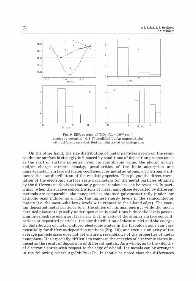
On the other hand, the size distribution of metal particles grown on the semi-
conductor surface is strongly influenced by conditions of deposition process (such
as the shift of surface potential from its equilibrium value, the photon energy
and/or charge carriers density, peculiarities of the ionic adsorption and
mass-transfer, surface diffusion coefficient for metal ad-atoms, etc.) strongly inf-
luence the size distribution of the resulting species. This plague the direct corre-
lation of the electronic surface state parameters for the metal particles obtained
by the different methods so that only general tendencies can be revealed. In part-
icular, when the surface concentrations of metal nanophase deposited by different
methods are comparable, the nanoparticles obtained galvanostatically (under low
cathodic bias) induce, as a rule, the highest-energy levels in the semiconductor
matrix (i.e. the most «shallow» levels with respect to the c-band edge). The vacu-
um-deposited metal particles form the states of minimal energy, while the nuclei
obtained photocatalytically under open circuit conditions induce the levels posses-
sing intermediate energies. It is clear that, in spite of the similar surface concent-
rations of deposited particles, the size distribution of these nuclei and the energe-
tic distribution of metal-induced electronic states in the forbidden zone can vary
essentially for different deposition methods (Fig. 10), and even a similarity of the
average particle sizes does not yet ensure a resemblance of the properties of metal
nanophase. It is especially difficult to compare the energies of electronic states in-
duced as the result of deposition of different metals. As a whole, as to the «depth»
of electronic states with respect to the edge of c-band, the metals can by arranged
in the following order: Ag≤Pd≤Pt<<Cu. It should be noted that the differences
74 A. I. Kulak, E. A. Streltsov,D. V. Sviridov
2.0 2.4 2.8
–0.8
–0.4
0.0
0.4
0.8 c
b
a
hν,eV
0 1 2 30
2
4
6 b
d, nm
0 1 20
2
4
6
a
d, nm
0 2 40
2
4c
d, nm
Fig. 9. EER spectra of TiO2 (Nd ≈ 1018 cm–3,
electrode potential –0.8 V) modified by Ag nanoparticles
with different size distribution illustrated by histograms
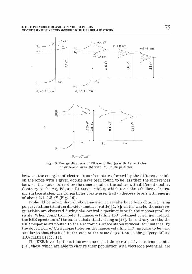
between the energies of electronic surface states formed by the different metals
on the oxide with a given doping have been found to be less then the differences
between the states formed by the same metal on the oxides with different doping.
Contrary to the Ag, Pd, and Pt nanoparticles, which form the «shallow» electro-
nic surface states, the Cu particles create essentially «deeper» levels with energy
of about 2.1–2.2 eV (Fig. 10).
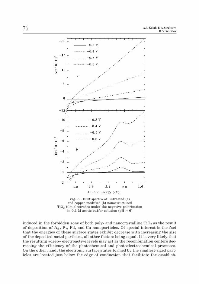
It should be noted that all above-mentioned results have been obtained using
polycrystalline titanium dioxide (anatase, rutile) [1, 3]; on the whole, the same re-
gularities are observed during the control experiments with the monocrystalline
rutile. When going from poly- to nanocrystalline TiO2 obtained by sol-gel method,
the EER spectrum of the oxide substantially changes [23]. In contrary to this, the
EER response attributed to the electronic surface states induced, for instance, by
the deposition of Cu nanoparticles on the nanocrystalline TiO2 appears to be very
similar to that obtained in the case of the same deposition on the polycrystalline
TiO2 matrix (Fig. 11).
The EER investigations thus evidences that the electroactive electronic states
(i.e., those which are able to change their population with electrode potential) are
75ELECTRONIC STRUCTURE AND CATALYTIC PROPERTIESOF OXIDE SEMICONDUCTORS MODIFIED WITH FINE METAL PARTICLES
EC
EF
EV
2.4
0eV
2.5
0eV
»
Pt Pd Cu
2.3
0eV
2.1
5eV
EC
EF
EV
2.3
8eV
2.5
0eV
»
r=0.8 nm
r=1.8 nmr=3÷5 nm
EC
EF
»
EV
N N
N
d d
d
=5 =5⋅ ⋅10 10
10
17 19
19
cm cm
cm
–3 –3
–3
2.8
eV
0.4 eV0.2 eV
Ag Ag
a
b
2.1
eV
=
Fig. 10. Energy diagrams of TiO2 modified (a) with Ag particles
of different sizes, (b) with Pt, Pd,Cu particles
induced in the forbidden zone of both poly- and nanocrystalline TiO2 as the result
of deposition of Ag, Pt, Pd, and Cu nanoparticles. Of special interest is the fact
that the energies of these surface states exhibit decrease with increasing the size
of the deposited metal particles, all other factors being equal. It is very likely that
the resulting «deep» electroactive levels may act as the recombination centers dec-
reasing the efficiency of the photochemical and photoelectrochemical processes.
On the other hand, the electronic surface states formed by the smallest-sized part-
icles are located just below the edge of conduction that facilitate the establish-
76 A. I. Kulak, E. A. Streltsov,D. V. Sviridov
Fig. 11. EER spectra of untreated (a)
and copper modified (b) nanostructured
TiO2 film electrodes under the negative polarization
in 0.1 M acetic buffer solution (pH = 6)
ment of the electron equilibrium between metal particles and conduction band.
Hence, it is very probable that such particles would function as modifying agent
improving the electrocatalytic properties of a semiconductor in dark processes.
4. EFFECT OF THE DEPOSITION OF METAL NANOPARTICLESON THE ELECTROCATALYTIC ACTIVITY
OF SEMICONDUCTOR ELECTRODES
The wide-bandgap semiconductors typically possess very low electrocatalytic
activity [3,20,26]. Thus, at the electrode potentials higher than the flat-band po-
tential (Efb), TiO2 electrodes with ordinary doping (Nd = 1017– 1019 cm–3) are cha-
racterized by the extremely small current densities (0.1 – 10 ìA/cm2) even in the presen-ce of such strong reducing agents as sodium boron hydride, hypophosphite, and
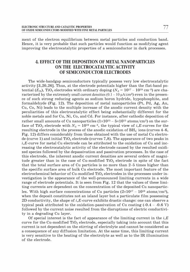
formaldehyde (Fig. 12). The deposition of metal nanoparticles (Pt, Pd, Ag, Au,
Cu, Co, Ni) leads to the multiple increase of the anodic current density with the
peculiarities of this electrocatalytic effect being substantially different for the
noble metals and for Cu, Ni, Co, and Cd. For instance, after cathodic deposition of
rather small amounts of Cu nanoparticles (1×10¹⁵– 5×10¹⁵ atoms/cm2) on the sur-
face of TiO2 electrode with Nd = 1019 cm–3, the typical view of i,E-curves for the
resulting electrode in the process of the anodic oxidation of BH4- ions (curves 4–6,
Fig. 12) differs considerably from those obtained with the use of metal Cu electro-
de (curve 1) and initial TiO2 electrode (curves 7,8). The appearance of two peaks in
i,E-curve for metal Cu electrode can be attributed to the oxidation of Cu and inc-
reasing the electrocatalytic activity of the electrode caused by the resulted oxidi-
zed species followed by the depassivation and passivation processes. In the case of
this electrode, the inherent anodic current densities are several orders of magni-
tude greater than in the case of Cu-modified TiO2 electrode in spite of the fact
that the total surface area of Cu particles is no more than 2–5 times higher than
the specific surface area of bulk Cu electrode. The most important feature of the
electrochemical behavior of Cu-modified TiO2 electrodes in the processes under in-
vestigation is the appearance of the well-pronounced limiting currents in a wide
range of electrode potentials. It is seen from Fig. 12 that the values of these limi-
ting currents are dependent on the concentration of the deposited Cu nanopartic-
les. With high surface concentrations of Cu particles (2×10¹⁷– 1018 atoms/cm2),
when the deposit constitutes not an island layer but a particulate film possessing
2D conductivity, the shape of i,E-curve exhibits drastic change: one can observe a
typical peak attributed to the oxidation-passivation of Cu coating (-0.4 – -0.6 V)
followed by the current noise resulted from the disruptions of electric conductivi-
ty in a degrading Cu layer.
Of special interest is the fact of appearance of the limiting current in the i,Ecurve for the Cu-modified TiO2 electrode, especially taking into account that this
current is not dependent on the stirring of electrolyte and cannot be considered as
a consequence of any diffusion limitation. At the same time, this limiting current
is very sensitive to the heating of the electrolyte as well as to the IR illumination
of the electrode.
77ELECTRONIC STRUCTURE AND CATALYTIC PROPERTIESOF OXIDE SEMICONDUCTORS MODIFIED WITH FINE METAL PARTICLES
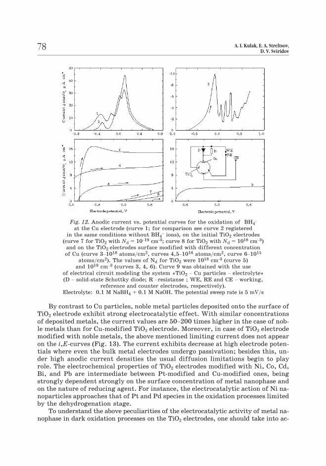
By contrast to Cu particles, noble metal particles deposited onto the surface of
TiO2 electrode exhibit strong electrocatalytic effect. With similar concentrations
of deposited metals, the current values are 50–200 times higher in the case of nob-
le metals than for Cu-modified TiO2 electrode. Moreover, in case of TiO2 electrode
modified with noble metals, the above mentioned limiting current does not appear
on the i,E-curves (Fig. 13). The current exhibits decrease at high electrode poten-
tials where even the bulk metal electrodes undergo passivation; besides this, un-
der high anodic current densities the usual diffusion limitations begin to play
role. The electrochemical properties of TiO2 electrodes modified with Ni, Co, Cd,
Bi, and Pb are intermediate between Pt-modified and Cu-modified ones, being
strongly dependent strongly on the surface concentration of metal nanophase and
on the nature of reducing agent. For instance, the electrocatalytic action of Ni na-
noparticles approaches that of Pt and Pd species in the oxidation processes limited
by the dehydrogenation stage.
To understand the above peculiarities of the electrocatalytic activity of metal na-
nophase in dark oxidation processes on the TiO2 electrodes, one should take into ac-
78 A. I. Kulak, E. A. Streltsov,D. V. Sviridov
Fig. 12. Anodic current vs. potential curves for the oxidation of BH4-
at the Cu electrode (curve 1; for comparison see curve 2 registered
in the same conditions without BH4– ions), on the initial TiO2 electrodes
(curve 7 for TiO2 with Nd = 10–19 cm-3; curve 8 for TiO2 with Nd = 1018 cm–3)
and on the TiO2 electrodes surface modified with different concentration
of Cu (curve 3–1018 atoms/cm2, curves 4,5–1016 atoms/cm2, curve 6–1015
atoms/cm2). The values of Nd for TiO2 were 1018 cm-3 (curve 5)
and 1019 cm–3 (curves 3, 4, 6). Curve 9 was obtained with the use
of electrical circuit modeling the system «TiO2 – Cu particles – electrolyte»
(D – solid-state Schottky diode; R –resistanse ; WE, RE and CE – working,
reference and counter electrodes, respectively).
Electrolyte: 0.1 M NaBH4 + 0.1 M NaOH. The potential sweep rate is 5 mV/s
count the differences in the electrocatalytic properties inherent in the deposited me-
tals, on the one hand, and the data on the energy distribution of electronic states in-
duced by the nanoparticles of these metals in a forbidden zone of TiO2 electrode, on
the other hand. A peculiar shape of i,E-curves obtained for the Cu-modified TiO2
electrodes and the appearance of the limiting currents can be attributed to the for-
mation and properties of Schottky barrier at the TiO2/Cu interface [1, 22, 26]. The
«deep» (with respect to the c-band edge) electronic surface states formed by the Cu
nanoparticles are unable to increase the permeability of Schottky barrier to the tun-
neling electrons. Since such a barrier is not completely perfect, there always exist le-
aking currents, this results in the increased electrocatalytic activity of the Cu-modi-
fied TiO2 electrodes in comparison with the naked ones. However, the attained incre-
ase of activity is essentially less than in the case of TiO2 electrodes modified by the
deposition of noble metals particles. In the latter case, the «shallow» electronic sur-
face states formed by metal nanoparticles, when their concentration is sufficiently
high, provide the typical «soft breakdown» of Schottky barrier. The nanoparticles of
metal fappears to be in an immediate electric contact with the semiconductor bulk,
the electrochemical behavior of the electrode being governed predominantly by the
electrocatalytic properties of these particles.
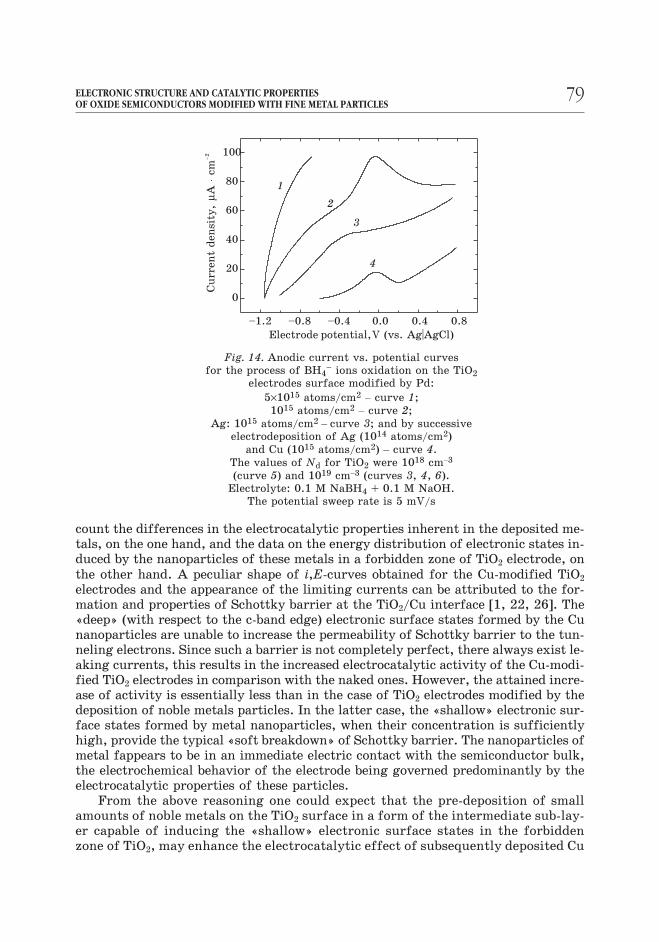
From the above reasoning one could expect that the pre-deposition of small
amounts of noble metals on the TiO2 surface in a form of the intermediate sub-lay-
er capable of inducing the «shallow» electronic surface states in the forbidden
zone of TiO2, may enhance the electrocatalytic effect of subsequently deposited Cu
79ELECTRONIC STRUCTURE AND CATALYTIC PROPERTIESOF OXIDE SEMICONDUCTORS MODIFIED WITH FINE METAL PARTICLES
–1.2 –0.8 –0.4 0.0 0.4 0.8
20
40
60
80
100
4
3
2
1
Current
densi
ty,
Acm
μ⋅
–2
Electrode potential,V (vs. Ag|AgCl)
0
Fig. 14. Anodic current vs. potential curves
for the process of BH4– ions oxidation on the TiO2
electrodes surface modified by Pd:
5×10¹⁵ atoms/cm2– curve 1;
1015 atoms/cm2– curve 2;
Ag: 1015 atoms/cm2– curve 3; and by successive
electrodeposition of Ag (1014 atoms/cm2)
and Cu (1015 atoms/cm2) – curve 4.
The values of Nd for TiO2 were 1018 cm–3
(curve 5) and 1019 cm–3 (curves 3, 4, 6).
Electrolyte: 0.1 M NaBH4 + 0.1 M NaOH.
The potential sweep rate is 5 mV/s
particles. Actually, the photocatalytic deposition of silver particles in amount of
5×10¹⁴ atoms/cm-2, which on its own only slightly increases the electrocatalytic
activity of TiO2 electrode, leads to 2–3-fold enhancement of the electrocatalytic
activity of Cu deposited in a relatively high concentration (1016– 1017 atoms/cm-2)
[22].
Notwithstanding to the fact that the efficiency of the anodic electrochemical
reaction in the case of metal-modified TiO2 electrode is limited by the value of the
leakage current for the reverse-biased Schottky diodes corresponding to the «me-tal/oxide» microjunctions, there exists a pronounced correlation between the elec-trocatalytic activity of TiO2-Me and bulk metal electrodes, with the efficiency of
BH4- oxidation increasing in the following manner: Cu < Ag < Ni < Pt. Such a be-
haviour can be attributed to the fact that the higher catalytic activity of the me-tal, the lower values of the potential drop in the Helmholtz layer reaching in case
of different TiO2-Me electrodes at the same current densities, that, in its turn, re-sults in larger potential drop in the space charge layer. Such potential redistribu-tion, which can be described in terms of some kind of feedback, leads to the corres-ponding increase of the l efficiency of the electrochemical reaction on the me-
tal-modified semiconductor surface.
5. IMPEDANCE OF SEMICONDUCTOR OXIDEELECTRODES MODIFIED WITH METAL PARTICLES
The effect of fine metal particles deposited onto the surface of semiconductor
electrodes on the frequency and potential dependencies of the electrochemical ca-
pacity of metal-modified semiconductor electrode is mainly due to the appearance
of the capacitance corresponding to the surface (interfacial) states (Css) and the
capacitance of the Helmholtz layer at the metal/electrolyte interface. The latter
factor is well-pronounced only in the condition of effective electron exchange bet-
ween metal particles and semiconductor bands, as with the noble metals cathodi-
cally-deposited onto the surface of film TiO2 electrodes. In the simplest case, the
equivalent circuit which mimic the behaviour of such electrode system can be re-
presented by two arms, connected in parallel, which correspond to free semicon-
ductor surface contacted with electrolyte and the surface of metal particles, res-
pectively. If especial precautions in order to exclude the presence of reducing me-
tal ions in the solution are not taken, the substantial changes in the electronic sta-
tes on the uncovered semiconductor surface represented by the corresponding
changes in the equivalent circuit may take place.
It is evident that the adequate description of electrode impedance in the case
of the actual contact between the surface-modified semiconductor and electrolyte
represents a very complicated problem due to the appearance of some hardly mea-
sured parameters associated with the particle size effects and the contributions of
surface and interfacial electronic states. Because of this, we shall restrict our con-
sideration to the simplest situation, when metal particles act as a set of metal mic-
roelectrodes electrically connected with the bulk of a semiconductor without the
formation of Schottky barrier at the metal/semiconductor interface, assuming
that the average size of these particles is sufficiently large to leave the properties
of the contact unaffected.
80 A. I. Kulak, E. A. Streltsov,D. V. Sviridov
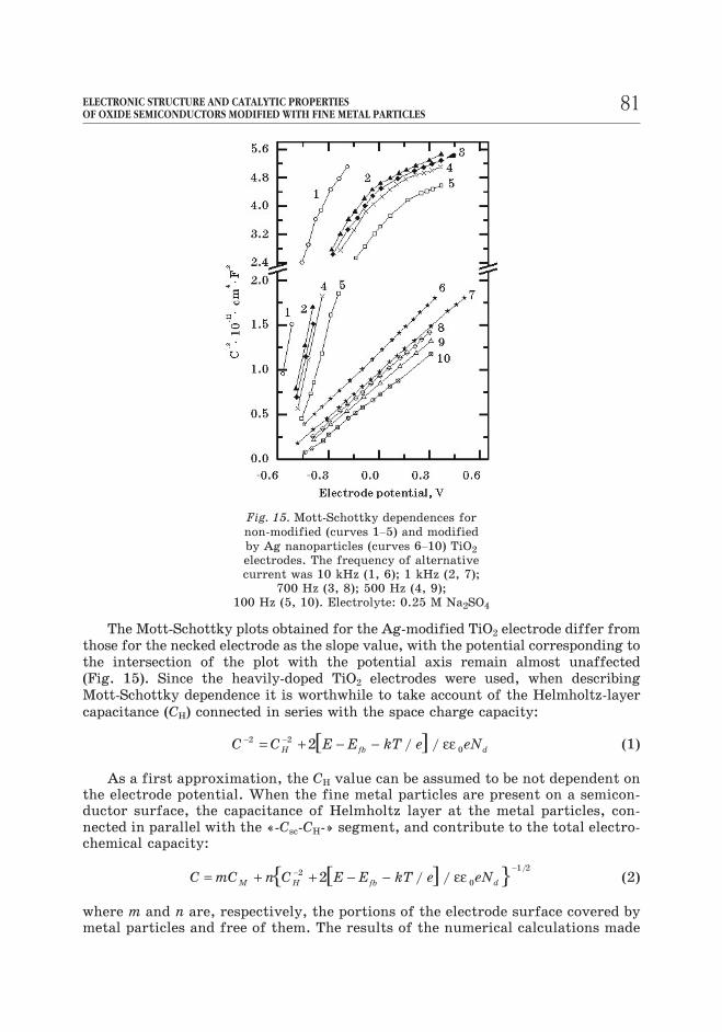
The Mott-Schottky plots obtained for the Ag-modified TiO2 electrode differ from
those for the necked electrode as the slope value, with the potential corresponding to
the intersection of the plot with the potential axis remain almost unaffected
(Fig. 15). Since the heavily-doped TiO2 electrodes were used, when describing
Mott-Schottky dependence it is worthwhile to take account of the Helmholtz-layer
capacitance (CH) connected in series with the space charge capacity:
[ ]C C E E kT e eNÍ fb d
− −= + − −2 2
02 / / εε (1)
As a first approximation, the CH value can be assumed to be not dependent onthe electrode potential. When the fine metal particles are present on a semicon-ductor surface, the capacitance of Helmholtz layer at the metal particles, con-nected in parallel with the «-Csc-CH-» segment, and contribute to the total electro-chemical capacity:
[ ]{ }Ñ mC n C E E kT e eNM H fb d= + + − −− −2
0
1 2
2 / //
εε (2)
where m and n are, respectively, the portions of the electrode surface covered bymetal particles and free of them. The results of the numerical calculations made
81ELECTRONIC STRUCTURE AND CATALYTIC PROPERTIESOF OXIDE SEMICONDUCTORS MODIFIED WITH FINE METAL PARTICLES
Fig. 15. Mott-Schottky dependences for
non-modified (curves 1–5) and modified
by Ag nanoparticles (curves 6–10) TiO2
electrodes. The frequency of alternative
current was 10 kHz (1, 6); 1 kHz (2, 7);
700 Hz (3, 8); 500 Hz (4, 9);
100 Hz (5, 10). Electrolyte: 0.25 M Na2SO4
with the use of the above equation suggest that the introduction of the capaci-tance of the metal particles into the equivalent circuit of the electrode systemleads to the changes in a slope of Mott-Schottky plots corresponding to the formalincrease of Nd value (Fig. 16). Thus a correction derived from the capacity ofmetal microelectrodes on a semiconductor surface should be introduced into thecommonly accepted determination of Nd value from the slope of Mott-Schottkycurves:
[ ]{ }{ }N
N
mC n Ñ E E kT e eN
n C E E
d
d
M Í fb d
H f
*/
/ /=
+ + − −
+ −
− −
−
2
0
1 2 3
2
2
2
εε
[ ]{ }{ }b dkT e eN−−
/ //
εε 0
1 2 3 (3)
The above ratio is dependent on the electrode potential, this dependence beco-
ming more pronounced with the increase of both m value and the difference bet-
ween the electrode potential and Efb (Figs. 15, 16).
Describing the Mott-Schottky dependences of semiconductor electrodes modi-
fied with fine metal particles, it is reasonable to take into account the contributi-
on of the capacitance of the electronic surface state induced by the chemisorpti-
on/reduction of ions and formation of metal ad-atoms and clusters. Taking into
account the charge of these electronic states (Qss) one can draw inference about
the shift of the extrapolation point of the Mott-Schottky plot by the following va-
lue:
′ = + + −E E kT e Q C N Cfb ss H sc d H/ / /εε 2 2 .
82 A. I. Kulak, E. A. Streltsov,D. V. Sviridov
0.4 0.8
0
2
4
Csc CH
CM
E-Efb, V
Ñ10
cm
F–2
–11
4–2
⋅⋅
⋅
Fig. 16. Equivalent circuit representing
the electrode system
«TiO2 -Ag nanoparticles- electrolyte»
and calculated Mott-Schottky curves
for different portions of the electrode surface
covered by metal particles (m):
0 (curve 1); 0.02 (curve 2); 0.2 (curve 3).
CH = 10 ìF/cm2;
CM = 20 ìF/cm2; Nd = 1.5×1018 cm–3
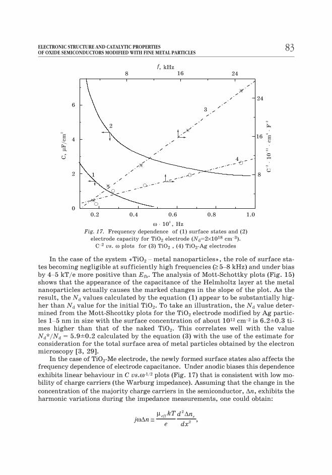
In the case of the system «TiO2 – metal nanoparticles», the role of surface sta-
tes becoming negligible at sufficiently high frequencies (≥5–8 kHz) and under bias
by 4–5 kT/e more positive than Efb. The analysis of Mott-Schottky plots (Fig. 15)
shows that the appearance of the capacitance of the Helmholtz layer at the metal
nanoparticles actually causes the marked changes in the slope of the plot. As the
result, the Nd values calculated by the equation (1) appear to be substantially hig-
her than Nd value for the initial TiO2. To take an illustration, the Nd value deter-
mined from the Mott-Shcottky plots for the TiO2 electrode modified by Ag partic-
les 1–5 nm in size with the surface concentration of about 1012 cm–2 is 6.2±0.3 ti-
mes higher than that of the naked TiO2. This correlates well with the value
Nd*/Nd = 5.9±0.2 calculated by the equation (3) with the use of the estimate for
consideration for the total surface area of metal particles obtained by the electron
microscopy [3, 29].
In the case of TiO2-Me electrode, the newly formed surface states also affects the
frequency dependence of electrode capacitance. Under anodic biases this dependence
exhibits linear behaviour in C vs.ω-1/2 plots (Fig. 17) that is consistent with low mo-
bility of charge carriers (the Warburg impedance). Assuming that the change in the
concentration of the majority charge carriers in the semiconductor, Δn, exhibits the
harmonic variations during the impedance measurements, one could obtain:
j nkT
e
d n
dx
eff eωμ
ΔΔ
≅2
2 ,
83ELECTRONIC STRUCTURE AND CATALYTIC PROPERTIESOF OXIDE SEMICONDUCTORS MODIFIED WITH FINE METAL PARTICLES
0.2 0.4 0.6 0.8 1.00
2
4
6
C,
F/cm
μ2
8 16 24
8
16
24
4
3
2
1
ω ⋅ 10 , Hz3
f, kHz
Ñ10
cm
F–2
–11
4–2
⋅⋅
⋅
Fig. 17. Frequency dependence of (1) surface states and (2)
electrode capacity for TiO2 electrode (Nd=2×1018 cm–3).
C–2 vs. ω plots for (3) TiO2 , (4) TiO2-Ag electrodes
where μeff is an effective mobility of charge carriers, the other symbols have their
traditional meaning. Taking into account the boundary condition
limx
en→
=0
0Δ
one could obtain the following solution of this equation:
Δ Δn n xj kT
ee s
eff= −⎛
⎝⎜
⎞
⎠⎟
⎡
⎣⎢
⎤
⎦⎥
−
exp
/ω μ 1 2
, where ΔneE
kT
e
kTEs
sc
sc= −ln 1,
where ΔEsc is potential drop in the space charge layer. The differentiation with
respect of x yields the following equation for electrode impedance:
Z kTn
e
j kT
e
e eff= 2
ω μ.
As the result, the electrode capacity appears to be governed by:
CkT
e ne eff
− =2
3 22
ωμ
The decreased slope of the C vs.ω–1/2 dependence in case of TiO2-Ag electrode
(Fig. 17) is formally consistent with higher mobility of charge carriers as compa-
red to the naked electrode that points to the increased permeability of the space
charge layer in the presence of silver nanoparticles (0.5–2.5 nm in size) on the
TiO2 surface. In other words, upon Ag deposition additional channels of charge
transfer appears to be activated, in particular, due to the redistribution of the po-
tential drop among the Helmholtz layer and space charge layer facilitates the soft
breakdown of the Schottky barrier.
6. INTERACTION OF METAL NANOPARTICLES WITH THE ASSOCIATESOF DONOR DEFECTS IN THE OXIDE SEMICONDUCTORS
The peculiarities of the interactions in the system «metal nanoparticles-semi-
conductor oxide» makes the deposition of metals a very sensitive tool permitting
to probe the semiconductor surface and to obtain a valuable information on the
segregation of donor centers typical of moderately and heavily doped semiconduc-
tors. It is clear that during the contact deposition of metals the nucleation on the
TiO2 surface occurs at the sites of donor location, especially at the donor clusters.
The process of oxidation of donor centers due to their interaction with metal ions
do not propagate interior the semiconductor bulk to the depth larger than several
oxide lattice constants because of limitations due the diffusion of oxygen accom-
panying the oxidation of donor centers. To explain the experimentally observed
appearance of a rather small concentration of large Ag particles on the TiO2 elect-
rodes, account must be given to the possibility of lateral electron transfer from
84 A. I. Kulak, E. A. Streltsov,D. V. Sviridov
neighboring donor centers via the mechanism typical to the electroless deposition
of metals. In any case, metal nanoparticles deposited as the result of the interacti-
on of semiconductor donor centers with metal ions prove to be localized at the si-
tes corresponding to the donor clusters. In a similar manner, during the depositi-
on of metal particles onto the cathodically-biased TiO2 electrode in a solution con-
taining metal ions, the growth of metal phase will be also localized at the sites of
the surface exposure of the donor clusters. Just these sites possess the enhanced
electrocatalytic activity as compared with the surface of stoichiometric oxide and
are responsible for the formation of the additional channels providing the unim-
peded charge transfer through the space charge region. Actually, a peculiar «de-
coration» of donor centers and donor clusters by metal nanoparticles occurs as the
result of the contact deposition of metal nanoparticles. The increased electrocata-
lytic activity of the wide-band-gap semiconductor electrodes resulted from the de-
position of metal nanoparticles on their surface may be also regarded as a «decora-
tion» of special type. In case of oxide semiconductors (e.g., WO3), the role of donor
clusters in the formation of the elrctrocatalytical behaviour of electrode can be re-
vealed by the selective electrochemical deposition of dielectric polymer, such as
poly-o-phenylenediamine permitting to blockade the abruptions of donor clusters
at the electrode surface [30].
As a whole, the discussed results evidences that the charge transfer through
the oxide semiconductor / electrolyte interface is governed by the local electroche-
mical processes at the surface of «microelectrodes» corresponding to the donor
clusters, rather than by tunneling of electrons through the semiconductor space
charge region.
CONCLUSIONS
The morphology of metal nanophase formed on the surface of wide-bandgap
semiconductor oxides via the contact, photocatalytic, or photoelectrochemical de-
position is substantially dependent on concentration, bulk distribution, and ener-
gy characteristics of donor defects in the semiconductor substrate. As a rule, the
necessary condition for the formation of the smallest-sized particles in the hig-
hest surface concentration is the maximum shift of the surface potential of semi-
conductor from its equilibrium value during metal deposition. This is part of the
reason for the experimentally observed fact that the particles formed in the condi-
tion of photocatalytic deposition are characterized by less average size and cover
superior portion of surface than those obtained under cathodic deposition, all ot-
her factors being equal.
The generation of electronic surface states in a forbidden zone of the semicon-
ductor by the deposition of metal nanoparticles is the major factor determining
the efficiency of electron exchange between metal particles and semiconductor
bulk and the efficiency of electrocatalytic process as a whole. According to the
electrolyte electroreflectance spectroscopic measurements, Ag, Pd, and Pt nano-
particles induce the «shallow» (with respect to the c-band edge) surface states in
the forbidden zone of TiO2, which provide near-unimpeded electron exchange bet-
85ELECTRONIC STRUCTURE AND CATALYTIC PROPERTIESOF OXIDE SEMICONDUCTORS MODIFIED WITH FINE METAL PARTICLES
ween metal particles and semiconductor c-band. As the size of metal particles inc-
reases, the surface state levels in TiO2 become more «deep» in relation to the edge
of c-band. Thus the modification of the energy structure of surface states, e.g. by
depositing metal nanophase of definite morphology or using the successive depo-
sition of different metals opens the fresh opportunities in exerting an effective
control over the electrocatalytic, photocatalytic, and photoelectrochemical pro-
perties of metal-loaded semiconductors.
REFERENCES
1. Kulak A. I. Electrochemistry of Semiconductor Heterostructures. Minsk, Univ.Press,
1986. 191 p.
2. Kulak A. I. The investigation of electrochemical and photoelectrochemical processes
on the titanium dioxide films. Thesis (Ph.D), Minsk, Belarusian State Univ., 1980.
204 p.
3. Kulak A. I. Photoelectrochemical and photochemical processes in systems based on the
semiconductor heterostructures. Thesis (D.Sc.), Minsk, Belarusian State Univ., 1990.
420 p.
4. Kulak A. I., Sviridov V.V., Poznyak S.K.,Makuta I. D. and Streltsov E. A. Vesti Acad.
Nauk BSSR. Ser.khim.nauk, ¹ 4, 24–31 (1987).
5. Kulak A. I., Streltsov E. A., and Sviridov D. V. Pat USSR (G 01 N 127/46) ¹ 1597814.
6. Talapin D. V., Sviridov D. V. and Kulak A. I. J. Electroanal. Chem., 442, 99–105 (1998).
7. Talapin D. V., Poznyak S. K., Sviridov D. V. and Kulak A. I. Surf. Sci., 454–456,
1046–1051 (2000).
8. Talapin D. V., Sviridov D. V. and Kulak A. I. Electrokhimiya, 37, ¹ 3, 313–320 (2001).
9. Sviridov D. V. and Kulak A. I. Elektrokhimiya, 22, No 1, 83–89 (1986).
10. Sviridov D. V., Poznyak S. K., Sviridov V.V. and Kulak A. I. Vesti Acad. Nauk BSSR.
Ser.khim.nauk, ¹ 6, 25–30 (1985).
11. Streltsov E. A., Sviridov V. V., Kulak A. I., Mychko D. I. and Malchenko S. N. Mater.
Chem. Phys., 25, ¹ 3, 315–322 (1990).
12. Streltsov E. A., Sviridov D. V. and Kulak A. I. Electrokhimiya, 20, ¹ 12, 1671–1674
(1984).
13. Sviridov D.V. and Kulak A.I. Khimiya vysokhich energij, 24, ¹ 3, 226–231 (1990).
14. V.V. Sviridov In: Nonsilver Photographic Processes (Ed. by Kartuzhansky A.L.), Khi-
miya, Leningrad, 242–307 (1984)
15. Utochkina S.P., Kuntcevitch N.I. and Sviridov D.V. Z. nauchn. prikl. fotogr. kinema-
togr., 34, ¹ 2, 189–194 (1990).
16. Poznyak S.K. and Kulak A.I. Electrochim. Acta, 35, ¹ 11/12, 1941–1947 (1990).
17. Poznyak S. K. and Kulak A. I. Khimiya vysokhich energij, 24, ¹ 1, 46–51 (1990).
18. Poznyak S.K. and Kulak A.I. J. Electroanal. Chem., 278, ¹ 1, 227–247 (1990).
19. Streltsov E.A., Kulak A.I., Sviridov D.V. and Pakhomov V.P. Elektrokhimiya, 19, ¹ 4,
546–548 (1983).
20. Streltsov E. A., Lazorenko–Manevich R. M., Pakhomov V. P. and Kulak A. I. Elektrokhi-
miya, 19, ¹ 3, 365–368 (1983).
21. Streltsov E. A., Kulak A.I. and Lazorenko-Manevich R.M. Elektrokhimiya, 20, ¹ 2,
211–214 (1984).
22. Kulak A. I., Kokorin A. I. and Sviridov D. V. J. Mater. Res., 16, ¹ 8, 2357–2361 (2001).
86 A. I. Kulak, E. A. Streltsov,D. V. Sviridov
23. Poznyak S. K., Pergushov V. I., Kokorin A. I., Kulak A. I. and Schläpfer C. W. J. Phys.
Chem., 103, ¹ 8, 1308–1315 (1999).
24. Poznyak S. K., Kokorin A.I. and Kulak A. I. J. Electroanal. Chem., 442, 99–105 (1998).
25. Kulak A. I., Sviridov V. V., Pakhomov V. P. and Shchukin G. L. Elektrokhimiya, 16, ¹ 1,
104–107 (1980).
26. Streltsov E. A., Pakhomov V. P., Lazorenko-Manevich R. M. and Kulak A. I. Elektrokhi-
miya, 19, ¹ 2, 232–235 (1983).
27. Streltsov E. A., Lazorenko-Manevich R.M., Pakhomov V.P. and Kulak A.I. Electrokhi-
miya, 19, ¹ 8, 1148 (1983).
28. Sviridov D. V. and Kulak A. I. Solar Energy Mater. Solar Cells, 39, ¹ 1, 45–53 (1995).
29. Sviridov D. V., Kulak A. I. and Streltsov E. A. Vestnik Belarus. Univ., Ser.2, ¹ 1, 8–11
(1986).
30. Sviridov D. V. and Kulak A. I. Thin Solid Films, 198, 191–198 (1991).
87ELECTRONIC STRUCTURE AND CATALYTIC PROPERTIESOF OXIDE SEMICONDUCTORS MODIFIED WITH FINE METAL PARTICLES