electronic supplementary information (esi) real-time ... · electronic supplementary material (esi)...
TRANSCRIPT
1
Electronic Supplementary Information (ESI)
Real-time optical diagnostics of graphene growth induced by
pulsed chemical vapor deposition
Alexander A. Puretzky*a, David B. Geohegan
b, Sreekanth Pannala
b, Murari Regmi
b,
Christopher M. Rouleau b, Norbert Thonnard
b, and Gyula Eres
b
1. Modeling of Gas Dynamics
We have used general purpose CFD (Computational Fluid Dynamics) software
called MFIX (Multiphase Flow with Interphase eXchanges).1-3
For this work, we have
only employed the single-phase capabilities of this software and the following continuity,
momentum, species, and energy equations are solved. The complex geometry of the
reactor utilizes the recently implemented Cartesian cut-cell technique in MFIX.4
Continuity Equation
( )
( )
Momentum Equation
( )
( ) (
)
where,
[(
)
]
Species Equation
( )
( )
(
)
Electronic Supplementary Material (ESI) for NanoscaleThis journal is © The Royal Society of Chemistry 2013

2
Energy Equation
[
]
(
) [
]
The above equations are spatially discretized using a finite volume technique
(first-order upwinding in this case) and an implicit backward Euler method is used for
time discretization. At
each time step, MFIX uses
Picard fixed point iteration
to solve the set of coupled,
highly nonlinear equations
that arise from the
discretization of transport
and conservation laws. The set of nonlinear equations is linearized using the SIMPLE5
formulation of fluid velocity correction and pressure correction. For each variable, a
system of sparse, non-symmetric linear equations corresponding to a regular seven-point
stencil on a logically rectangular grid are solved.
The computational setup of the pulse reactor is shown in the schematic above (not
to scale). The mass-flow rate along with species composition is prescribed at the inlet.
The temperature profile on the wall is prescribed. This case is run with very small time-
steps (100 µs – 1 ms) to resolve the injected pulse width of 10 ms (the C2H2 pulse is
distributed over 10 ms to account for the diffusion into the t-junction), and the pulse is
injected after 0.5 seconds. By 0.5 seconds the solution has reached stationary state
starting with initial conditions (reference temperature and constant velocity set to zero).
The properties of the gases are calculated using the BURCAT thermochemical database.
Fig. S1. Schematic of the computational setup (plane cuts
through the center line of the inlet and outlet pipes of the
reactor) along with the boundary conditions.
Electronic Supplementary Material (ESI) for NanoscaleThis journal is © The Royal Society of Chemistry 2013
3
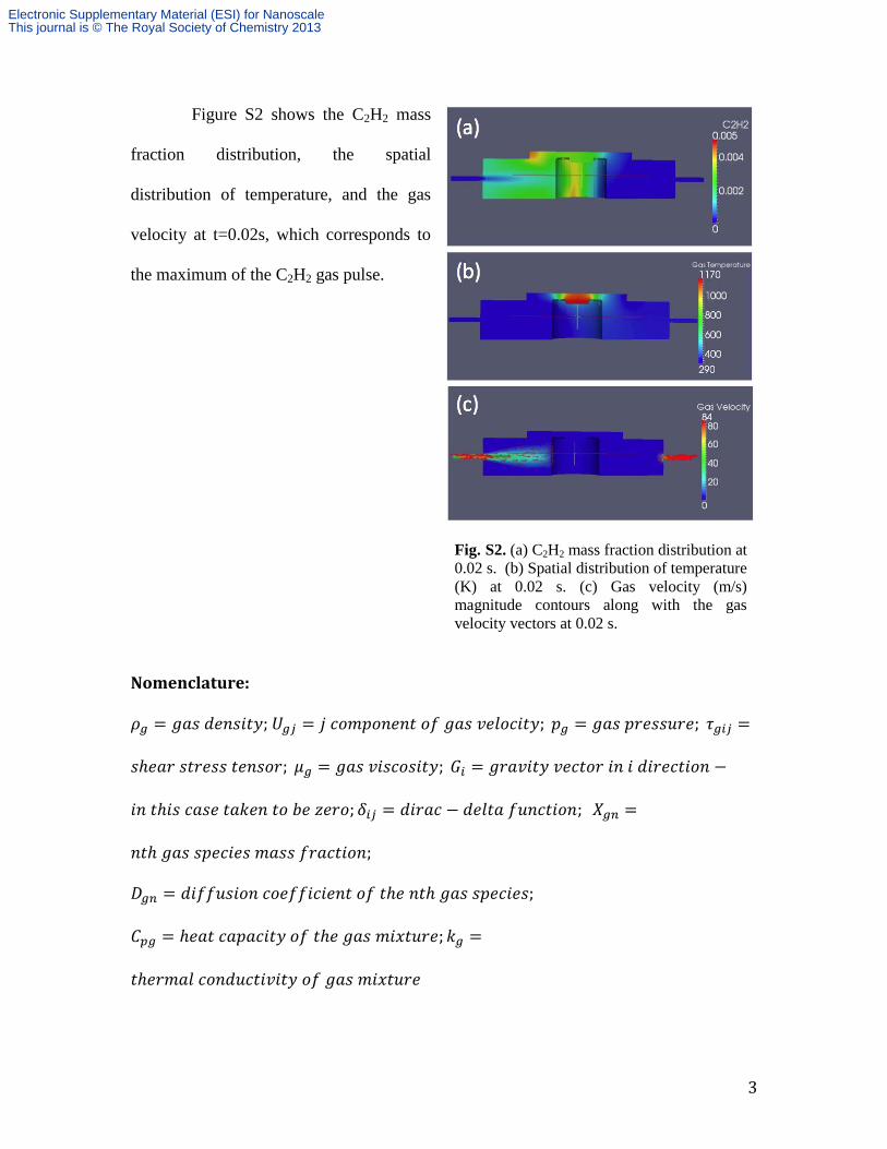
Figure S2 shows the C2H2 mass
fraction distribution, the spatial
distribution of temperature, and the gas
velocity at t=0.02s, which corresponds to
the maximum of the C2H2 gas pulse.
Nomenclature:
;
;
Fig. S2. (a) C2H2 mass fraction distribution at
0.02 s. (b) Spatial distribution of temperature
(K) at 0.02 s. (c) Gas velocity (m/s)
magnitude contours along with the gas
velocity vectors at 0.02 s.
Electronic Supplementary Material (ESI) for NanoscaleThis journal is © The Royal Society of Chemistry 2013
4
References
[1] M. Syamlal, S. Pannala, in Computational Gas-Solids Flows and Reacting
Systems: Theory, Methods and Practice, (Eds. S. Pannala, M. Syamlal, T.
O’Brien) IGI Global, Hershey, PA, 2010.
[2] M. Syamlal, MFIX documentation: numerical techniques (1998).
[3] M. Syamlal, W. Rogers, T.G. O’Brien, MFIX Documentation: Theory Guide,
DOE/METC-94/1004 (DE94000087) (Morgantown Energy Technology Center)
1993.
[4] J.-F. Dietiker, T. Li, R. Garg and M. Shahnam, Powder Technology 235 (0), 696-
705 (2013).
[5] A. Prosperetti, S. Sundaresan, S. Pannala, D. Z. Zhang, in Computational Methods
for Multiphase Flow, (Eds. A. Prosperetti, G. Tryggvason) Cambridge University
Press, Cambridge, 2007.
Electronic Supplementary Material (ESI) for NanoscaleThis journal is © The Royal Society of Chemistry 2013
5
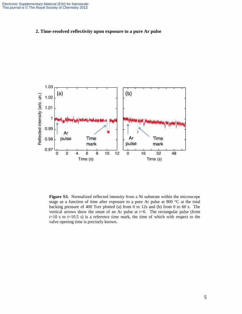
2. Time-resolved reflectivity upon exposure to a pure Ar pulse
Figure S3. Normalized reflected intensity from a Ni substrate within the microscope
stage as a function of time after exposure to a pure Ar pulse at 800 °C at the total
backing pressure of 400 Torr plotted (a) from 0 to 12s and (b) from 0 to 60 s. The
vertical arrows show the onset of an Ar pulse at t=0. The rectangular pulse (from
t=10 s to t=10.5 s) is a reference time mark, the time of which with respect to the
valve opening time is precisely known.
Electronic Supplementary Material (ESI) for NanoscaleThis journal is © The Royal Society of Chemistry 2013

6
3. Raman map of graphene transferred to a SiO2/Si substrate.
Figure S4. (a) Optical image of graphene grown on a 0.5-m thick Ni film on SiO2/Si at 840 °C using
a 5% mix (see text) of C2H2 and transferred to a SiO2 (0.3m)/Si substrate using a standard procedure,
which involves spin-coating with PMMA followed by etching of the Ni film with HCl (10 volume %
aqueous solution) and removing the PMMA layer in acetone. The square in the center marks the area
used for Raman mapping. (b) Raman map (62m x 62m) of the I(2D)/I(G) ratios measured for
graphene transferred to a SiO2(0.3m)/Si substrate. The 12 dots on the map indicate the positions for
the corresponding Raman spectra shown in Fig. S5 (a) points 9-12 and (b) points 1-8. The map was
acquired using a 532nm excitation wavelength (laser spot size at the sample ~ 2 m) with 1s
acquisition time for each point and 2m increments.
Electronic Supplementary Material (ESI) for NanoscaleThis journal is © The Royal Society of Chemistry 2013

7
4. Selected Raman spectra of graphene transferred to a SiO2/Si substrate.
Figure S5. Selected set of the Raman spectra corresponding to the 12 dots marked on the Raman map
(see Fig. S4b). (a) Points 9-12 and (b) points 1-8.
Electronic Supplementary Material (ESI) for NanoscaleThis journal is © The Royal Society of Chemistry 2013

8
Raman
spectrum
number
(Fig. S4)
Raman
bands
Band
positions,
cm-1
(±1cm-1
)
Bandwidth
(FWHM),
cm-1
(±0.5 cm-1
)
I(2D)/I(G)
1 2D
G
2670
1584
25.7
19.5 11.0
2 2D
G
2699
1584
24.3
19.0 11.1
3 2D
G
2700
1584
24.3
19.0 13.3
4 2D
G
2700
1584
23.7
18.7 13.5
5 2D
G
2699
1584
26.3
19.9 10.7
6 2D
G
2699
1584
27.9
20.4 9.7
7 2D
G
2701
1584
39.5
20.2 4.5
8 2D
G
2700
1584
27.4
19.9 6.8
9 2D
G
2726
1583
21.1 0.8
10 2D
G
2703
1584
45.8
21.3 0.3
11 2D
G
2703
1584
73.0
21.3 0.6
12 2D
G
2699
1585
51.3
20.7 0.5
Table S1. Positions, bandwidths, and I(2D)/I(G) ratios estimated from the Raman spectra shown
in Fig. S4.
Electronic Supplementary Material (ESI) for NanoscaleThis journal is © The Royal Society of Chemistry 2013
9
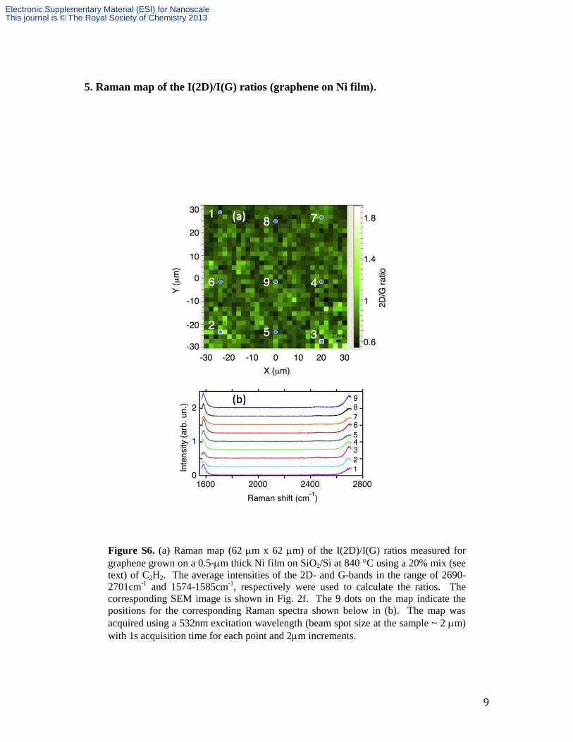
5. Raman map of the I(2D)/I(G) ratios (graphene on Ni film).
Figure S6. (a) Raman map (62 m x 62 m) of the I(2D)/I(G) ratios measured for
graphene grown on a 0.5-m thick Ni film on SiO2/Si at 840 °C using a 20% mix (see
text) of C2H2. The average intensities of the 2D- and G-bands in the range of 2690-
2701cm-1
and 1574-1585cm-1
, respectively were used to calculate the ratios. The
corresponding SEM image is shown in Fig. 2f. The 9 dots on the map indicate the
positions for the corresponding Raman spectra shown below in (b). The map was
acquired using a 532nm excitation wavelength (beam spot size at the sample ~ 2 m)
with 1s acquisition time for each point and 2m increments.
Electronic Supplementary Material (ESI) for NanoscaleThis journal is © The Royal Society of Chemistry 2013

10
6. Raman map of the I(2D)/I(G) ratios (transferred graphene on SiO2/Si substrate).
Figure S7. (a) Raman map (62 m x 62 m) of the I(2D)/I(G) ratios measured for
graphene grown on a 0.5-m thick Ni film on SiO2/Si at 840 °C using a 20% mix (see
text) of C2H2 and transferred to a SiO2 (0.5 m)/Si substrate. The map was acquired
using a 532nm excitation wavelength (laser spot size at the sample ~ 2 m) with 2s
acquisition time for each point and 2m increments. The 9 dots on the map indicate
the positions for the corresponding Raman spectra shown below in (b).
Electronic Supplementary Material (ESI) for NanoscaleThis journal is © The Royal Society of Chemistry 2013

11
7. Comparison of Raman spectra of single layer suspended graphene at 532 nm
and 404.5 nm
Figure S8. Raman spectrum of suspended single layer, single crystal graphene
grown on Cu foil by low pressure, continuous CVD and transferred to a 2000 mesh
microscope grid measured at 532 nm and 404.5 nm using the same spot. The
spectra are normalized to the intensities of the G-bands. These spectra demonstrate
that at 404.5 nm excitation the relative intensity of the 2D-band drops by factor of
3.7 when compared to operating at 532 nm.
Electronic Supplementary Material (ESI) for NanoscaleThis journal is © The Royal Society of Chemistry 2013
12
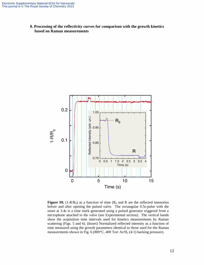
8. Processing of the reflectivity curves for comparison with the growth kinetics
based on Raman measurements
Figure S9. (1-R/R0) as a function of time (R0 and R are the reflected intensities
before and after opening the pulsed valve. The rectangular 0.5s-pulse with the
onset at 3.4s is a time mark generated using a pulsed generator triggered from a
microphone attached to the valve (see Experimental section). The vertical bands
show the acquisition time intervals used for kinetics measurements by Raman
scattering (Figs. 5 and 6). (Insert) Normalized reflected intensity as a function of
time measured using the growth parameters identical to those used for the Raman
measurements shown in Fig. 6 (800°C, 400 Torr Ar/H2 (4:1) backing pressure).
Electronic Supplementary Material (ESI) for NanoscaleThis journal is © The Royal Society of Chemistry 2013