elemental distributions and substrate rotation in .../file/fegtem6.pdf · superlattice hard pvd ......
TRANSCRIPT
Surface and Coatings Technology 183(2004) 275–282
0257-8972/04/$ - see front matter� 2003 Elsevier B.V. All rights reserved.doi:10.1016/j.surfcoat.2003.09.060
Elemental distributions and substrate rotation in industrial TiAlNyVNsuperlattice hard PVD coatings
Z. Zhou , W.M. Rainforth *, B. Rother , A.P. Ehiasarian , P.Eh. Hovsepian , W.-D. Munza a, b c c c¨
Department of Engineering Materials, The University of Sheffield, Sheffield S1 3JD, UKa
DMS GmbH, Lobtauer Str. 69, 01159 Dresden, Germanyb ¨Materials Research Institute, Sheffield Hallam University, Sheffield S1 1WB, UKc
Received 23 April 2003; accepted in revised form 19 September 2003
Abstract
Chemical distribution of individual layers within a TiAlNyVN multilayer structure was characterised using a field emissiongun transmission electron microscope, coupled with energy-filtered elemental mapping and high-angle annular dark field imaging.Bright field TEM micrographs using zero-loss electrons indicated the presence of alternating TiAlN and VN layers with aperiodicity of;3 nm. Electron spectroscopic images(ESI) using the Ti-L and V-L edges were used to determine the Ti and2,3 2,3
V composition profiles of layers and confirmed the complementary distribution of Ti and V. ESI demonstrated an additionalmodulation super-imposed on the basic period of the coatings, which was confirmed by Z-contrast imaging using scanningtransmission electron microscopy. The additional modulation was related to the threefold rotational geometry used in the depositionprocess. Film growth and elemental distributions were therefore theoretically predicted in association with substrate rotation. Theexperimental compositional profiles and the prediction showed good agreement. The implications of the compositional modulationon key process parameters are discussed.� 2003 Elsevier B.V. All rights reserved.
Keywords: TiAlN yVN multilayers; Energy-filtered TEM; Substrate rotation; Numerical prediction
1. Introduction
Nanoscale multilayers, such as superlattices, haveemerged in recent years as wear-protective coatings dueto their superior hardness()60 GPa), and have receivedmuch interest in both fundamental research and indus-trial application. The hardness of a superlattice coatingwas found to be strongly dependent on the superlatticeperiodicity with a maximum hardness found at periodic-ity between 3 and 7.5 nm for TiNyVN w1x and 3–4 nmfor TiAlN yCrN w2x. Models for explaining the hardnessenhancement have been suggested on the basis of effectssuch as dislocation hindrance at the layer interfaces dueto differences in shear moduli and coherency strainsfrom lattice mismatch of the two materials in each layerof the bi-layersw3x. In parallel, a variety of superlatticePVD coatings, such as TiNyAlN, TiN yNbN, TiAlNy
*Corresponding author. Tel.:q44-114-222-2000; fax:q44-114-222-5943.
E-mail address: [email protected](W.M. Rainforth).
WN, TiAlN yCrN, TiAlCrYN and TiAlNyVN, typicallywith periods of 3–4 nm, have been economically man-ufactured and commercialised on an industrial scale bycombined steered cathodic arc evaporation and unbal-anced magnetron sputtering. The TiAlNyVN coatinginvestigated here is tailored for tribological applicationsbecause of its relatively low friction coefficient(ms0.4, pin-on-disc, Al O ball counterpart) in comparison2 3
to other wear-protective coatings(e.g. TiAlN ms0.7)and its extremely low sliding wearw4x.A typical industrial deposition machine, such as the
one used in this study(a Hauzer HTC 1000-4 ABS),has a characteristic substrate arrangement and threefoldrotation geometry to facilitate homogenous depositionon three-dimensional-shaped surfaces, such as cuttingtools. The superlattice periodicity is mainly determinedby the prime rotation speed of the substrate turntable,the cathode power, the pressure of the reactive gas andthe bias voltage applied on substrates during coatingdeposition. As a result of the substrate rotation, each
276 Z. Zhou et al. / Surface and Coatings Technology 183 (2004) 275–282
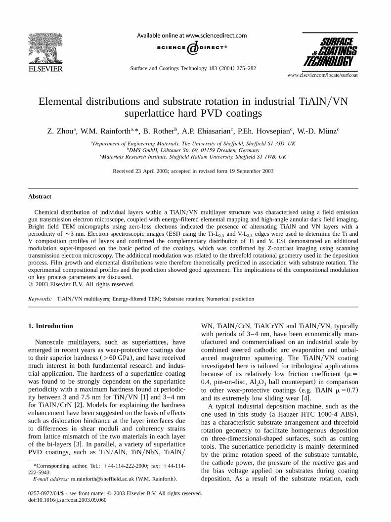
Fig. 1. Schematic top view of the arrangement of targets and substrateturntable in the deposition chamber used.
substrate surface is periodically exposed to a flux densityas well as to varying angles of particle current incidence.The effect of threefold rotation on the film growth ratehas been modelled and found to give rise to character-istic oscillationsw5–8x. The growth oscillations can beinfluenced by rotation radii, frequencies and frequencyratios of the basic rotations, as well as the number andposition of particle sources. Validation of the oscillationstructure has been performed for elemental concentra-tions in (Cr,Ti)N coatings by glow discharge opticalemission spectroscopy and Auger electron spectroscopydepth profiling w5x. However, both methods failed toreveal the details of high frequency oscillations due toresolution limitations. The extremely fine structures ofthe industrial superlattice coatings require state-of-the-art electron microscopy techniques to reveal local phys-ical and chemical structures as a function of positionwithin the coatingw9,10x.In this paper, the distributions of Ti and V in a
TiAlN yVN superlattice were characterised by field emis-sion gun transmission electron microscopy(FEGTEM)coupled with energy-filtered TEM(EFTEM) and Z-contrast imaging to determine the microstructure andcomposition distributions on the nanometer scale. Filmgrowth was predicted by applying a numerical model,which calculated normalized flux distributions andgrowth rates at a rotating sample surface. A comparisonbetween the TEM experimental results and the numericalcalculation is presented and discussed.
2. Experimental details
2.1. Substrate rotation geometry
TiAlN yVN superlattice coatings were grown on stain-less steel substrates in an industrial scale physical vapourdeposition coating machine. A schematic top view ofthe deposition geometry is shown in Fig. 1. The arrange-ment consists of four rectangular cathodes, which canbe operated either in steered cathodic arc mode or areto be used as unbalance magnetron sputtering sourcesw11x. Two adjacent pairs of cathodes, furnished withTiAl and V targets, respectively, have been used for theTiAlN yVN coating deposition by unbalanced magnetronsputtering in a mixed ArqN atmosphere(a partial2
pressure ratio of pAr:pNs2:1, corresponding to the2
transition from metallic to poisoned sputtering regime).The substrate rotation unit provides threefold rotationwith the main turntable rotating at a speed of 8 rpm(anti-clockwise) with 12 satellites centred on a circleD s500 mm�. Spindles are mounted on a twofoldRot1
rotation mechanism, which rotates at a rate determinedby a gear ratio of 99y27 to the main rotation, anti-clockwise. On each of the spindles, there are 10 substrateholders situated on a circleD s95 mm �. TheRot2
substrate holders are rotated in switched mode with fiveteeth embedded inside the substrate holder and one
switching point to facilitate a third turning, as shown inFig. 1. D is approximately 5 mm�. The substrateRot3
holders turned clockwise. Sputtering took place withoutmechanical shieldingyshutter or gas flow guide plates.Approximately 20 substrates were included in the coat-ing chamber for research investigation when depositionwas conducted. The mean deposition rate of the coatingwas;20 nmymin, with a substrate temperature of 4508C and a negative substrate bias of 95 V. More detailsabout the deposition are given in Ref.w4x.
2.2. TEM characterisation
Cross-sections of the superlattice coatings for TEMobservation were prepared. Two slices were cut from afilm ysubstrate and glued together using an epoxy resin,with coatings face to face. The resulting package wasmounted onto a disc grinder(Gatan, model 623), thenground and polished to a thickness of 40mm. Afterbeing glued to a copper support ring, the sample wasion-beam-thinned from both sides at an incidence angleof 158 by a Gatan duo ion-miller until close to perfora-tion, followed by final perforation at the glue-line usinga Gatan precision ion polishing system at"38.Since the periodicity of the TiAlNyVN bi-layers of
;3 nm is so small, it is essential to align the bi-layerinterface parallel to the incident electron beam prior todetermining the chemical distribution of layers, in par-ticular intermixing between layers. To ensure this con-dition, a columnar grain was tilted such that thesuperlattice diffraction spots were exactly symmetricalat either side of the transmitted and principal diffractionspot. Moreover, very thin regions of the sample, asdetailed below, were also used.
277Z. Zhou et al. / Surface and Coatings Technology 183 (2004) 275–282
Electron spectroscopic imaging was performed on aJEOL 2010F TEM operating with a field emission gunat 200 kV and equipped with a Gatan imaging filter(GIF). The spectra and images were recorded with theslow-scan CCD camera integrated into the GIF, usingthe procedures optimised by Hofer and co-workers, e.g.Refs. w12–14x. High gun emission currents and a largecondenser aperture were used to maximise current den-sity. Prior to acquiring spectroscopic images or EELspectra, atyl map(tssample thickness,lstotal inelas-tic scattering electron mean free path) was taken toensure thattyl-0.5 and therefore plural scatteringcould be ignored w15x. Spectroscopic images wereobtained using the Ti-L (455.5 eV) and V-L (5132,3 2,3
eV) ionisation edges. The three-window backgroundsubtraction method was used to generate elementalmaps. Additional images were acquired using the scan-ning TEM (STEM) unit coupled with a high-angleannular dark field detector(HAADF), which providesimage contrast that is also sensitive to the local chemicalcomposition w16x. All the experimental images wereacquired on the slow-scan CCD camera and all imageprocessing was performed usingGATAN digital micro-graph software.
3. Results and discussion
3.1. TEM experimental results
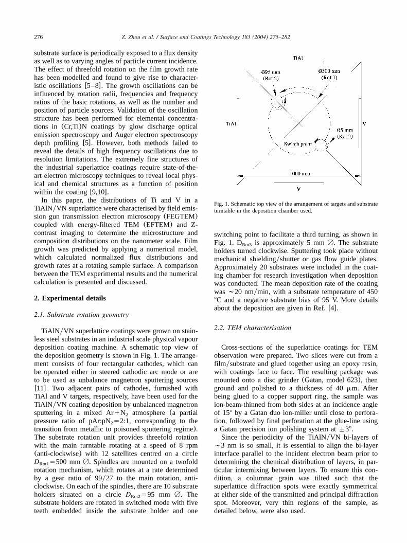
Fig. 2a gives a zero-loss EFTEM bright field imageof the multilayer from the middle of a TiAlNyVNsuperlattice coating. The micrograph was taken at amicroscope objective lens defocus in order to provideFresnel contrast, which accurately indicates the positionof the individual layersw17x. Inset is the selected areadiffraction pattern from this area. The superlattice dif-fraction spots are symmetrically located at both sides ofthe transmitted spot, which indicates that the bi-layerswere growing parallel to the(1 1 1) planes in this grain.Fig. 2b gives a line-scan showing the image intensityvariations in the selected area in Fig. 2a. An individualline-scan was found to have inadequate signal to noiseratio. In order to optimise the signal-to-noise ratio, aline-scan profile was derived from the integrated inten-sity from a box region, as indicated in Fig. 2. Sincewaviness of bi-layers is a common phenomenon invarious superlattice coatingsw4x (which is obvious inFig. 2), there is a risk of averaging intensity from theneighbouring layers with image analysis. However,efforts were made to minimise this effect by selecting abox from a region where the individual layers were asclose as possible to parallel. The bright field TEMmicrograph in conjunction with the intensity profiledemonstrated the presence of alternating TiAlN and VNlayers with an average periodicity of 3 nm. The bi-layerthickness was calculated from the peak-to-peak positionsof such intensity profiles. It was found that the bi-layer
thickness was not constant but varied in a systematicmanner, such as 3.1, 2.9, 2.9, 3.1, 3.1, 2.9, 3.1, 3.1, 2.9,2.9, 3.1, 2.9, 3.1, 2.9 and 3.4"0.5 nm, with some bi-layers apparently wider or thinner.Fig. 2c and e show electron spectroscopic images
(ESI) from the Ti-L and V-L edges, which con-2,3 2,3
firmed the complementary distribution of Ti and Vconcentrations. The integrated intensity of Ti and Vsignals as a function of distance was derived from theelemental maps using digital micrograph software andare presented in Fig. 2d and f. The ESI, in conjunctionwith concentration profiles, demonstrated an additionalmodulation super-imposed on the basic period ofcoatings.The additional modulation was also revealed by Z-
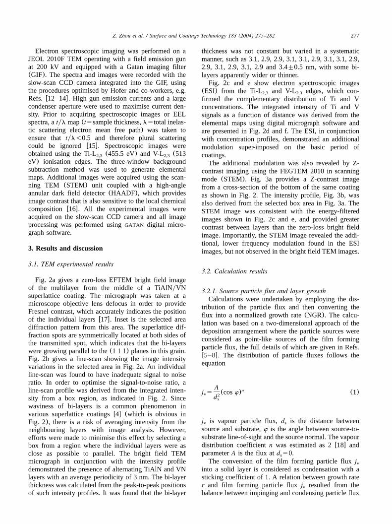
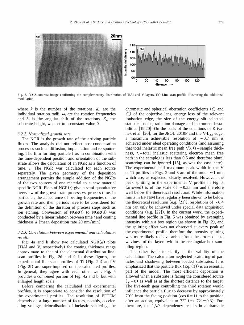
contrast imaging using the FEGTEM 2010 in scanningmode (STEM). Fig. 3a provides a Z-contrast imagefrom a cross-section of the bottom of the same coatingas shown in Fig. 2. The intensity profile, Fig. 3b, wasalso derived from the selected box area in Fig. 3a. TheSTEM image was consistent with the energy-filteredimages shown in Fig. 2c and e, and provided greatercontrast between layers than the zero-loss bright fieldimage. Importantly, the STEM image revealed the addi-tional, lower frequency modulation found in the ESIimages, but not observed in the bright field TEM images.
3.2. Calculation results
3.2.1. Source particle flux and layer growthCalculations were undertaken by employing the dis-
tribution of the particle flux and then converting theflux into a normalized growth rate(NGR). The calcu-lation was based on a two-dimensional approach of thedeposition arrangement where the particle sources wereconsidered as point-like sources of the film formingparticle flux, the full details of which are given in Refs.w5–8x. The distribution of particle fluxes follows theequation
A nj s (cosw) (1)v 2ds
j is vapour particle flux,d is the distance betweenv s
source and substrate,w is the angle between source-to-substrate line-of-sight and the source normal. The vapourdistribution coefficientn was estimated as 2w18x andparameterA is the flux atd s0.s
The conversion of the film forming particle fluxjvinto a solid layer is considered as condensation with asticking coefficient of 1. A relation between growth rater and film forming particle flux j resulted from thev
balance between impinging and condensing particle flux
278 Z. Zhou et al. / Surface and Coatings Technology 183 (2004) 275–282
Fig. 2. (a) Bright field TEM image(zero-loss filtered) of a cross-section in the middle of a TiAlNyVN superlattice coating. Inset is the selectedarea diffraction pattern with the left diffraction spot enlarged.(b) Line-scan profile of the intensity variation of the selected area in(a) showingthe alternating TiAl and V layers.(c and e) Ti and V elemental maps.(d and f) Line-scan profiles of Ti and V elemental distribution in theselected area indicated in corresponding elemental maps revealing the additional modulation.
densities, which was approximated as
mcrsyj cosa, 908-a-1808 (2a)vrc
rs0, 08-a-908 (2b)
where the average mass of a film forming particle ism , the density of the condensed layer isr and thec c
angle between the particle flux and the substrate normalvector isa. The calculation neglected scattering, shad-owing of j and re-sputtering due to the Ar ionq
v
bombardment during coating growth. Calculations ofr
under consideration of scattering, shadowing as well asparticle source extension(not point-like but line-likeparticle sources) produced practically identical resultsto those obtained by the above approach.The growth rate was related to the threefold rotation
through the sample positions:S Wcosv tqdŽ .i i
T Tk
U Xd (t)s d sin v tqd (3)Ž .s si i i8is1 T T
Vz Ys
279Z. Zhou et al. / Surface and Coatings Technology 183 (2004) 275–282
Fig. 3. (a) Z-contrast image confirming the complementary distribution of TiAl and V layers.(b) Line-scan profile illustrating the additionalmodulation.
where k is the number of the rotations,d are thesi
individual rotation radii,v are the rotation frequenciesi
and d is the angular shift of the rotations.Z , thei s
substrate height, was set to a constant value 0.
3.2.2. Normalized growth rateThe NGR is the growth rate of the arriving particle
fluxes. The analysis did not reflect post-condensationprocesses such as diffusion, implantation and re-sputter-ing. The film forming particle flux in combination withthe time-dependent position and orientation of the sub-strate allows the calculation of an NGR as a function oftime, t. The NGR was calculated for each sourceseparately. The given geometry of the depositionarrangement permits the simple addition of the NGRsof the two sources of one material to a new materialspecific NGR. Plots of NGR(t) give a semi-quantitativeoverview of the growth rate process vs. process time. Inparticular, the appearance of beating frequencies of thegrowth rate and their periods have to be considered forthe definition of the duration of process steps such asion etching. Conversion of NGR(t) to NGR(d) wasconducted by a linear relation between timet and coatingthicknessd (mean deposition rate 20 nmymin).
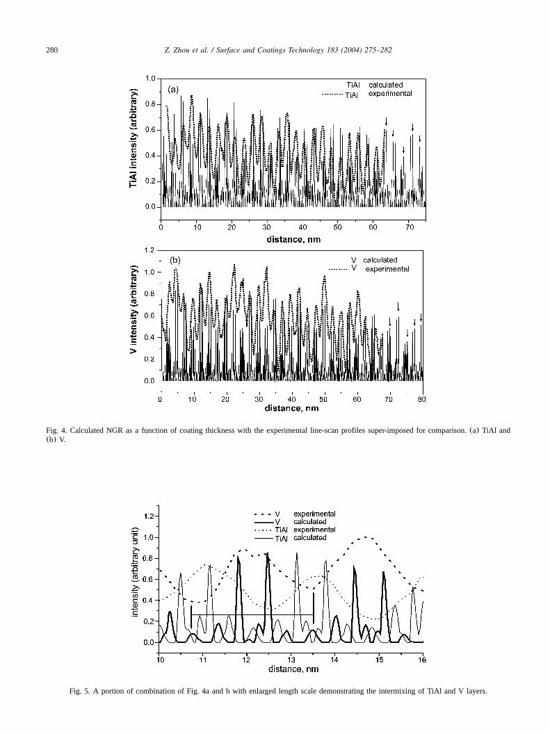
3.2.3. Correlation between experimental and calculationresultsFig. 4a and b show two calculated NGR(d) plots
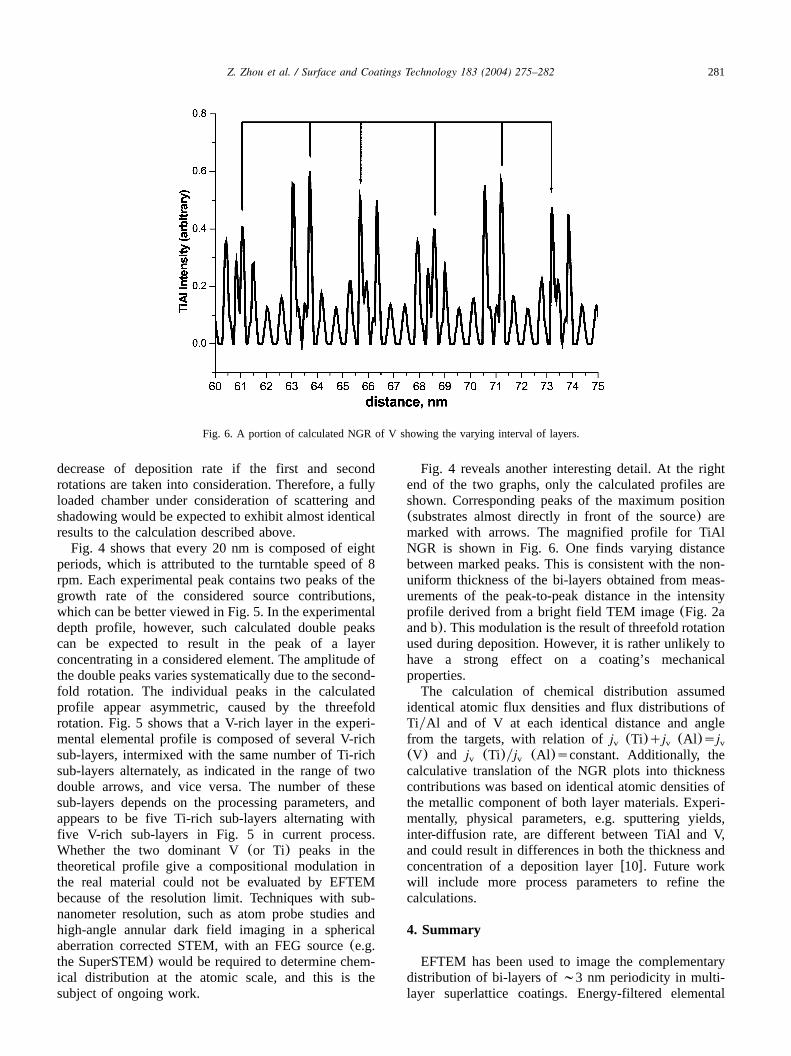
(TiAl and V, respectively) for coating thickness rangeapproximate to that of the elemental distribution line-scan profiles in Fig. 2d and f. In these figures, theexperimental line-scan profiles of Ti(Fig. 2d) and V(Fig. 2f) are super-imposed on the calculated profiles.In general, they agree with each other well. Fig. 5provides a combined portion of Fig. 4a and b, but withenlarged length scale.Before comparing the calculated and experimental
profiles, it is appropriate to consider the resolution ofthe experimental profiles. The resolution of EFTEMdepends on a large number of factors, notably, acceler-ating voltage, delocalisation of inelastic scattering, the
chromatic and spherical aberration coefficients(C andc
C ) of the objective lens, energy loss of the relevants
ionisation edge, the size of the energy slit selected,statistical noise, radiation damage and instrument insta-bilities w19,20x. On the basis of the equations of Kriva-nek et al.w20x, for the JEOL 2010F and the V-L edge,2,3
a maximum achievable resolution of;0.7 nm isachieved under ideal operating conditions(and assumingthat total inelastic mean free pathtyl (tssample thick-ness,lstotal inelastic scattering electron mean freepath in the sample) is less than 0.5 and therefore pluralscattering can be ignoredw15x, as was the case here).The experimental half maximum peak width in the Vor Ti profiles in Figs. 2 and 3 are of the order;1 nm,which are, as expected, clearly resolved. However, thepeak splitting in the experimental V profile in Fig. 5(arrowed) is of the scale of;0.35 nm and thereforewell below the theoretical resolution. While informationlimits in EFTEM have regularly been shown to be belowthe theoretical resolution(e.g.w21x), resolutions of;0.4nm can only be achieved under special data acquisitionconditions(e.g. w22x). In the current work, the experi-mental line profile in Fig. 5 was obtained by averagingintensity within a box region(as shown in Fig. 2), andthe splitting effect was not observed at every peak ofthe experimental profile, therefore the intensity splittingwas more likely to have arisen from the errors due towaviness of the layers within the rectangular box sam-pling region.The other issue to clarify is the validity of the
calculation. The calculation neglected scattering of par-ticles and shadowing between loaded substrates. It isemphasized that the particle flux(Eq.(1)) is an essentialpart of the model. The most efficient deposition isallowed when a substrate is facing the considered source(ws0) as well as at the shortest distance to the target.The five-teeth gear controlling the third rotation wouldinfluence the particle flux to decrease by approximately70% from the facing position(cos 0s1) to the positionafter an action, equivalent to 728 (cos 728s0.3). Fur-thermore, the 1yd dependency results in a dramatic2
280 Z. Zhou et al. / Surface and Coatings Technology 183 (2004) 275–282
Fig. 4. Calculated NGR as a function of coating thickness with the experimental line-scan profiles super-imposed for comparison.(a) TiAl and(b) V.
Fig. 5. A portion of combination of Fig. 4a and b with enlarged length scale demonstrating the intermixing of TiAl and V layers.
281Z. Zhou et al. / Surface and Coatings Technology 183 (2004) 275–282
Fig. 6. A portion of calculated NGR of V showing the varying interval of layers.
decrease of deposition rate if the first and secondrotations are taken into consideration. Therefore, a fullyloaded chamber under consideration of scattering andshadowing would be expected to exhibit almost identicalresults to the calculation described above.Fig. 4 shows that every 20 nm is composed of eight
periods, which is attributed to the turntable speed of 8rpm. Each experimental peak contains two peaks of thegrowth rate of the considered source contributions,which can be better viewed in Fig. 5. In the experimentaldepth profile, however, such calculated double peakscan be expected to result in the peak of a layerconcentrating in a considered element. The amplitude ofthe double peaks varies systematically due to the second-fold rotation. The individual peaks in the calculatedprofile appear asymmetric, caused by the threefoldrotation. Fig. 5 shows that a V-rich layer in the experi-mental elemental profile is composed of several V-richsub-layers, intermixed with the same number of Ti-richsub-layers alternately, as indicated in the range of twodouble arrows, and vice versa. The number of thesesub-layers depends on the processing parameters, andappears to be five Ti-rich sub-layers alternating withfive V-rich sub-layers in Fig. 5 in current process.Whether the two dominant V(or Ti) peaks in thetheoretical profile give a compositional modulation inthe real material could not be evaluated by EFTEMbecause of the resolution limit. Techniques with sub-nanometer resolution, such as atom probe studies andhigh-angle annular dark field imaging in a sphericalaberration corrected STEM, with an FEG source(e.g.the SuperSTEM) would be required to determine chem-ical distribution at the atomic scale, and this is thesubject of ongoing work.
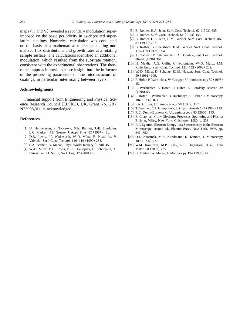
Fig. 4 reveals another interesting detail. At the rightend of the two graphs, only the calculated profiles areshown. Corresponding peaks of the maximum position(substrates almost directly in front of the source) aremarked with arrows. The magnified profile for TiAlNGR is shown in Fig. 6. One finds varying distancebetween marked peaks. This is consistent with the non-uniform thickness of the bi-layers obtained from meas-urements of the peak-to-peak distance in the intensityprofile derived from a bright field TEM image(Fig. 2aand b). This modulation is the result of threefold rotationused during deposition. However, it is rather unlikely tohave a strong effect on a coating’s mechanicalproperties.The calculation of chemical distribution assumed
identical atomic flux densities and flux distributions ofTiyAl and of V at each identical distance and anglefrom the targets, with relation ofj (Ti)qj (Al)sjv v v
(V) and j (Ti)yj (Al)sconstant. Additionally, thev v
calculative translation of the NGR plots into thicknesscontributions was based on identical atomic densities ofthe metallic component of both layer materials. Experi-mentally, physical parameters, e.g. sputtering yields,inter-diffusion rate, are different between TiAl and V,and could result in differences in both the thickness andconcentration of a deposition layerw10x. Future workwill include more process parameters to refine thecalculations.
4. Summary
EFTEM has been used to image the complementarydistribution of bi-layers of;3 nm periodicity in multi-layer superlattice coatings. Energy-filtered elemental
282 Z. Zhou et al. / Surface and Coatings Technology 183 (2004) 275–282
maps(Ti and V) revealed a secondary modulation super-imposed on the basic periodicity in as-deposited super-lattice coatings. Numerical calculation was conductedon the basis of a mathematical model calculating nor-malized flux distributions and growth rates at a rotatingsample surface. The calculations identified an additionalmodulation, which resulted from the substrate rotation,consistent with the experimental observations. The theo-retical approach provides more insight into the influenceof the processing parameters on the microstructure ofcoatings, in particular, intermixing between layers.
Acknowledgments
Financial support from Engineering and Physical Sci-ence Research Council(EPSRC), UK, Grant No. GRyN23998y01, is acknowledged.
References
w1x U. Helmersson, S. Todorova, S.A. Barnett, J.-E. Sundgren,L.C. Markert, J.E. Greene, J. Appl. Phys. 62(1987) 481.
w2x D.B. Lewis, I.P. Wadsworth, W.-D. Munz, R. Kuzel Jr., V.¨Valvoda, Surf. Coat. Technol. 116–119(1999) 284.
w3x S.A. Barnett, A. Madan, Phys. World January(1998) 45.w4x W.-D. Munz, D.B. Lewis, P.Eh. Hovsepian, C. Schonjahn, A.¨¨
Ehiasarian, I.J. Smith, Surf. Eng. 17(2001) 15.
w5x B. Rother, H.A. Jehn, Surf. Coat. Technol. 62(1993) 635.w6x B. Rother, Surf. Coat. Technol. 64(1994) 155.w7x B. Rother, H.A. Jehn, H.M. Gabriel, Surf. Coat. Technol. 86–
87 (1993) 207.w8x B. Rother, G. Ebersbach, H.M. Gabriel, Surf. Coat. Technol.
116–119(1999) 694.w9x J. Cawley, J.M. Titchmarsh, L.A. Donohue, Surf. Coat. Technol.
86–87(1996) 357.w10x H. Meidia, A.G. Cullis, C. Schonjahn, W.-D. Munz, J.M.¨ ¨
Rodenburg, Surf. Coat. Technol. 151–152(2002) 209.w11x W.-D. Munz, D. Schulze, F.J.M. Hauzer, Surf. Coat. Technol.¨
50 (1992) 169.w12x F. Hofer, P. Warbichler, W. Grogger, Ultramicroscopy 59(1995)
15.w13x P. Warbichler, F. Hofer, P. Hofer, E. Letofsky, Micron 29
(1998) 63.w14x F. Hofer, P. Warbichler, B. Buchmayr, S. Kleber, J. Microscopy
184 (1996) 163.w15x P.A. Crozier, Ultramicroscopy 58(1995) 157.w16x T. Walther, C.J. Humphreys, J. Cryst. Growth 197(1999) 113.w17x R.E. Dunin-Borkowski, Ultramicroscopy 83(2000) 193.w18x B. Chapman, Glow Discharge Processes: Sputtering and Plasma
Etching, Wiley, New York, Chichester, 1980, p. 233.w19x R.F. Egerton, Electron Energy-loss Spectroscopy in the Electron
Microscope, second ed., Plenum Press, New York, 1996, pp.347–352.
w20x O.L. Krivanek, M.K. Kundmann, K. Kimoto, J. Microscopy180 (1995) 277.
w21x W.M. Rainforth, M.P. Black, R.L. Higginson, et al., ActaMater. 50(2002) 735.
w22x B. Freitag, W. Mader, J. Microscopy 194(1999) 42.