elp2im: efficient and low power bitwise operation
TRANSCRIPT

2020 IEEE International Symposium on High Performance Computer Architecture
ELP2IM: Efficient and Low Power Bitwise OperationProcessing in DRAM
Xin Xin1, Youtao Zhang2, and Jun Yang 1
1Electrical and Computer Engineering Department, University of Pittsburgh2Department of Computer Science, University of Pittsburgh
[email protected], [email protected], [email protected]
ABSTRACTRecently proposed DRAM based memory-centric architec-tures have demonstrated their great potentials in addressingthe memory wall challenge of modern computing systems.Such architectures exploit charge sharing of multiple rowsto enable in-memory bitwise operations. However, existingdesigns rely heavily on reserved rows to implement com-putation, which introduces high data movement overhead,large operation latency, large energy consumption, and lowoperation reliability.
In this paper, we propose ELP2IM, an efficient and lowpower processing in-memory architecture, to address theabove issues. ELP2IM utilizes two stable states of senseamplifiers in DRAM subarrays so that it can effectively re-duce the number of intra-subarray data movements as well asthe number of concurrently opened DRAM rows, which ex-hibits great performance and energy consumption advantagesover existing designs. Our experimental results show thatthe power efficiency of ELP2IM is more than 2× improve-ment over the state-of-the-art DRAM based memory-centricdesigns in real application.
1. INTRODUCTIONModern system performance is hindered by memory sub-
system, known as "the memory wall", due to the high costof data movement [1, 2]. Particularly, for big-data appli-cations, the limited bandwidth of the off-chip bus betweenmemory and processor cannot meet the increasing demand ofdata. A significant amount of power during data movementis consumed, leading to system energy inefficiency. To tacklethis problem, near-data processing (NDP) has been proposedas a solution. In DRAM-based NDP, logic units (LU) arebuilt close to but outside DRAM arrays. Examples of NDPinclude HMC [3, 4], Automata [5] and DRISA [6]. NDPdelivers good performance due to the removal of volume datamovement and high processing speed in LUs. However, highspeed of LUs is attributed to their high complexity, whichusually occupy large die area and decreases the density ofmemory. For example, the adder in DRISA takes 51% ofarea, and the routing matrix in Automata occupies about 30%of the chip [5]. Complex LUs on a separate layer of an HMCare constrained by not only area but also power consump-tion. Moreover, large area of LUs increases the complexityof DRAM technology, as LUs and DRAM cells are usually
not compatible in technology process [7].Alternatively, true in-memory computing, a.k.a. processing-
in-memory (PIM), directly integrates logic functions intomemory arrays. PIM keeps integrity of memory and realizeshigh-bandwidth calculation with light area overhead. Notethat NDP and PIM are not contradicting approaches. PIMembeds operations inside memory array, offloading thoselogic from NDP design. Recently, a DRAM-based PIM archi-tecture, termed Ambit [8], has been proposed for bulk bitwiseoperations. It implements basic logic operations based onan inter-cell charge sharing mechanism, which can exploitfull internal bandwidth inside DRAM. It provides great op-portunities to accelerate applications with large amount ofbitwise operations [9, 10, 11]. Nevertheless, we observed thatits performance is still impeded by several aspects.
First, each logic operation in Ambit requires triple-rowactivation (TRA) which imposes high power consumptionthat challenges inherent power constraint, e.g. tFAW , and re-duces bank level parallelism [12, 13]. The frequent copiesamong different memory rows in each logic operation gen-erally double or even triple the number of row activation inone access. In other words, when a memory array is per-forming a logic operation, there is little to no power left forother banks to perform regular memory accesses. Second,each logic operation in Ambit requires many commands, orlong latency, giving that each command in DRAM is alreadya long-latency operation. For example, an XOR operationrequires 7 commands (or DRAM cycles), totaling ∼363ns(DDR3-1600 [14]). Third, Ambit requires to reserve a groupof rows, typically 8, near sense amplifiers for each calculation.Even though those reserved rows can be used for storing data,it is still necessary to migrate them when Ambit switches tocalculation mode. Those are additional capacity and latencyoverhead in the array. Fourth, charge sharing among the cellsopened by TRA can become unreliable with process varia-tion and bitline coupling effect. This is because those cellsmay not have equal capacitance which could lead to less thanideal charge sharing [15]. Finally, the coupling effect worsenthe situation by narrowing the sensing margin, as we willquantify in our experiments.
To address the aforementioned problems, we propose a newtechnique by creating a new state, termed pseudo-prechargestate, in DRAM access. In this state, bitline voltage is regu-lated by sense amplifier (SA) instead of the precharge logic.Logic operation can be implemented by using the regulated
1

bitline to access the next source cell.Pseudo-precharge based approach offers two benefits: First,
it provides the opportunity to implement an in-place logicoperation, which completes the calculation directly in thedestination cells, instead of the reserved cells. Thereby, itreduces data copy to the reserved cells, which further di-minishes operation cycles and the reserved rows. For thebasic logic operation, we shorten the average latency by up to1.23×. Second, based on the method, charge sharing in eachcycle just involves one cell, which is similar to the regularDRAM access. Thereby, it reduces the number of row acti-vations and can maintain the same sensing margin as regularDRAM. In real applications, we save up to 2.45× row acti-vations, thereby expanding bank level parallelism by 2.45×.Significant improvement in reliability is also achieved. Thecontributions of this paper are summarized as follows:
• We present a lightweight mechanism to implement bulkbitwise operation in DRAM, termed ELP2IM, whichefficiently reduces the number of commands for eachkind of logic operation.
• ELP2IM not only lowers the power consumption, butalso relieves power constraint problem by reducing thenumber of activated rows of each command.
• ELP2IM also significantly saves the reserved space,only retaining one reserved row, and improves the oper-ation reliability.
• We propose two strategies considering different sizesof DRAM subarray. We also categorize six primitivesfor ELP2IM, and further improve the performance bybetter scheduling of those primitives.
2. BACKGROUND AND RELATED WORK
2.1 Overview of DRAMA DRAM chip traditionally adopts hierarchical structure
from cell matrices to subarrays and to banks. While onesubarray horizontally consists of many cell matrices, a bankhas multiple subarrays connected using the global bitlines.Each bank can be operated by the memory controller inde-pendently. Each cell matrix comprises a large number of cellswhich are built by an access transistor and a capacitor (1T1C).Multiple cells are connected by a local bitline with a senseamplifier (SA) which also acts as a row buffer [8, 16].
Figure 1(a) illustrates the internal structure of one columnin the cell matrix. The SA is constructed as a latch usingtwo CMOS inverters, which has two voltage inputs (at node1 and 2) and one enable EN signal. As we discuss next, weprovide different voltages at node 1 and 2 at different times toenable the precise memory access. The precharge unit (PU) ispowered by a Vdd/2 source and controlled by the EQ signal.The DRAM bitline usually possesses a noticeable parasiticcapacitor, which exhibits large impact on access speed.
Figure 1(b) indicates an access sequence in DRAM. It canbe divided into two states: precharge and activate [17]. In theprecharge state, the PU is enabled to set both the bitline pairand the SA to Vdd/2. The activate state can be further dividedinto three phases — access, sense, and restore. In the access
Figure 1: (a) Concise structure of a DRAM column, (b)Basic states (or phases) in a DRAM access, (c) SA sup-ply voltage controller, (d) Precharge unit with separatecontrol signals
phase, the wordline is enabled to share the charges in the cellcapacitor with the bitline, which leads to a voltage variationon the bitline. In the sense phase, the SA is enabled to sensethe slight variation on the bitline. Finally, in the restore phase,the SA continuously charges the bitline and the cells untiltheir voltage reaches Vdd or Gnd. The DRAM subarray mayreturn to the precharge state afterwards.
2.2 Related WorkRecently, several DRAM based PIM designs, such as such
as Rowclone, Ambit, Dracc, ROC etc., have been proposed[8, 18, 19, 20]. They implement bulk bitwise operation intra-subarray with high throughput and efficiency.
2.2.1 RowCloneRowClone [18] implements data copy between different
rows in the same subarray. When DRAM completes the re-store phase, the SA can retain the state if precharge is not en-abled. Therefore, row-to-row data copy can be implementedby sequentially activating the target row after completingthe restore phase of the source row. This row copy methodcontains two back-to-back activate states and one prechargestate, referred as an Activate-Activate-Precharge (AAP) prim-itive in [18]. The AAP is close to 2× latency of a regularActivate-Precharge (AP) access, as activate state occupiesa large proportion of the access time. To reduce the AAPlatency, Ambit adds an extra row decoder for the reservedrows. Thereby, two rows in the same subarray but belong todifferent decoder domains can be activated simultaneously.This separated row decoder strategy offers the opportunityto overlap the two Activates in AAP, hence, significantlysaving the time. To distinguish from AAP, we define the over-lapped Activate-Activate-Precharge as oAAP in this article.Although the overlapped AAP (oAAP) is only 4 ns longerthan AP (49 ns), it aggravates the burden on charge pump,which drives the wordlines.
2.2.2 AmbitAmbit exploits the analog operation of DRAM technology
to perform bitwise operations. The critical step in the mech-
2

anism is to activate three DRAM cells on the same bitlineat the same time [8], termed Triple-Row Activate (TRA).Thereby, if any two (or all) of the three cells, termed A, B,and C, are ‘1’s, the voltage on the bitline will be above Vdd/2after charge sharing. Otherwise, the voltage will drop belowVdd/2 when only one or none of them is ‘1’. The result can bewritten as: R = AB + BC + AC. If we define C = 1 in advance,the operation will perform A OR B. Likewise, A AND Bcan be performed with C = 0. For completeness, the NOToperation is implemented in a modified dual-connected cell,where one additional access transistor is attached. Benefit-ing from the high parallel actions of DRAM cells in a row,logic computation of large bit-vectors could be significantlyaccelerated.
Directly implementing TRA with cell A, B, and C is infea-sible because general row decoder cannot activate three rowssimultaneously. This also destroys the original data. There-fore, Ambit requires a group of reserved rows with specialrow decoder for TRA. For example, to implement an ORoperation, it first copies two variables A and B to the reservedrows. Then it copies C, which is ‘1’ as a preceding definitionfor OR logic. Finally, it calculates the result via TRA. Thisprocess involves four cycles in total. For more complex logic,it will consume more cycles. Therefore, performance ofAmbit is impeded by the redundant data movement process,which copies A, B, and C before the true calculation.
In addition, Ambit also suffers from power constraint, re-liability, and overhead of reserved rows, which has beenintroduced in Section 1.
2.2.3 Other related worksDeng et al. modify several subarray rows with extra transis-
tors to improve the performance of Ambit based acceleratorfor CNN calculation [19]. However, the multiple cycles ofan operation still hinder the speed. For example, it takes13 cycles to complete an ADD calculation, which amountsto ∼ 630ns with 49ns cycle time [8]. In addition, the addi-tional transistors reduces area efficiency, which also increasesdesign complexity for DRAM fabrication process.
Li et al. propose a DRAM-based configurable accelerator,termed Drisa [6]. Different from previous works, Drisa com-pletes logic operation by directly integrating logic gates insubarray, thereby, exploiting the full internal bandwidth. Forthe design of logic part, it presents several strategies, such asNOR gate, mixed gates, and even adders. The area overheadvaries based on the complexity of integrated logic gates. Inthe case studies, the author claims the NOR or mixed de-sign is more efficient. But even for the simplest NOR baseddesign, it still increases 24% area overhead.
2.3 Structure ComparisonAmong the aforementioned studies, we choose Ambit as
the representative design for bitwise operation, because ofits relatively good efficiency and less modifications. Fig-ure 2 provides a general view of regular DRAM, Ambit, andELP2IM. Compared to the structure of regular DRAM [21],Ambit requests a special row decoder, which can simultane-ously pull up triple wordlines, to serve the reserved the rows,termed B-group. In the B-group, the last four rows are mod-ified into the two dual-contact cells, which provide buffers
for NOT operation. There is less modification in ELP2IM.Only one dual-contact-cell row, controlled by a small driver,is attached in each array.
Figure 2: Structure of regular DRAM(a), Ambit(b), andELP2IM(c)
Our design is built on open-bitline architecture, becauseall modern DRAM utilizes the open-bitline to achieve highdensity [22]. The detailed analysis of modification and relatedoverhead will be discussed in Section 5.2.
3. DESIGN OF ELP2IMIn this paper, we propose ELP2IM, a pseudo-precharge
approach, to complete logic operations through direct chargesharing with bitlines, which greatly reduces the latency andlowers the power consumption of DRAM based PIM oper-ations. We next motivate the design with two observations,elaborate the design details, and analyze different executionstrategies.
3.1 Observations
Figure 3: (a) Pseudo-precharge state, (b) Bitline over-write effect
3.1.1 Pseudo-precharge StatesWe exploit two stable yet non-traditional DRAM states,
referred to as pseudo-precharge states. As shown in Fig-ure 1(b), the supply voltage of an SA is switched periodicallywith the help of a voltage controller (Figure 1(c)). In particu-lar, the SA has its input voltages switched from Vdd and Gndat node 1 and 2, respectively, at activation state to the sameVdd/2 at prechage state. Having Vdd/2 supply voltage helpsto suppress the leakage power and improve the subsequentsensing accuracy.
Similar to that in recent studies [23], we study the SAworkflow and observe that, if in precharge state, only one ofthe two supplies shifts back to Vdd/2 while the other keepsits voltage level, the output of SA adjusts accordingly dueto rail-to-rail output character of the CMOS inverters [24].That is, the SA stays at a stable state. Figure 3(a) shows anexample, during activate state, bitline and bitline are chargedto Vdd and Gnd respectively. If only Vdd shifts to Vdd/2,then bitline will follow the change, while bitline will remainthe same. To distinguish this voltage shifting process fromprecharge state, we term it as pseudo-precharge state.
3

Figure 4: OR Operation of two cases: ‘1’+‘0’ (Case 1) and ‘0’+‘0’ (Case 2)
Since the voltage shifting technique is compatible withregular CMOS circuit design and incurs small overhead, it hasbeen adopted as structure optimization to suppress leakageinduced power in latches or registers [23, 25, 26]. Instead ofreducing power consumption, we leverage this technique toassist logic operation in DRAM, and what we change is onlythe control sequence for the voltage shift of SA.
3.1.2 Overwrite ProcessOur other observation is on a stable yet non-traditional
cell write operation. During precharge state, if only bitline ischarged to Vdd/2, while bitline keeps its value, the followingaccessed cell will be overwritten by the bitline value. Sincethe bitline capacitor (Cb) is generally much larger (2∼4×)than the cell capacitor (Cc) [27, 30], it dominates the bitlinevoltage level during charge sharing. Figure 3(b) shows an ex-ample, where logic ‘1’ on bitline is reserved during precharge.In the next activate state, the accessed cell is overwritten by‘1’. Note, to enable the overwriting process, we need to mod-ify the precharege unit, as shown in Figure 1(d) — we splitthe EQ signal to two such signals, EQ and EQb, such that wecan control each side independently.
For DRAM subarrays that have short bitlines, e.g., due tosmall capacity [28, 29], Cb may be close to, or even smallerthan, Cc, which prevents the overwriting process as we dis-cuss above. In this paper, we are to develop a simple strategyto enable reliable data overwrite by comparing the differencebetween bitline and bitline. We will elaborate the details inSection 4.
In summary, the above two observations expose stableyet non-traditional states and memory operations in DRAM,which provide promising opportunities that can be exploitedto speed up DRAM based processing-in-memory operations.
3.2 The Basic IdeaIntuitively, ELP2IM takes a two step approach to exploit
the pseudo-precharge states and overwrite operation — itfirst regulates the charge level of bitline capacitor (Cb) in thepseudo-precharge state; and then leverages the regulated Cb
to influence the next cycle DRAM access (overwrite or not),thereby completes logic operations.
Figure 4 illustrates how to implement a ‘two-cycle’ (nottwo normal memory cycles) OR operation with two specificexamples, ‘1’+‘0’ and ‘0’+‘0’ operations in case 1 and 2respectively. The initial values saved in the two cells are ‘1’and ‘0’ in case 1 (‘0’ and ‘0’ in case 2). For case 1, logic ‘1’is accessed in the activate state during the first cycle. Thena pseudo-precharge state is inserted, where the Gnd of SAis switched to Vdd/2. As explained in section 3.1, underthis condition, the bitline can hold its voltage level of Vdd.In the following precharge state, only bitline is charged toVdd/2 by PU, which is similar to the second observation.Thereby, in activate state of the second cycle, the accessedcell is overwritten by the reserved bitline value. For case2, logic ‘0’ is accessed in the activate state during the firstcycle. In the next state, bitline is driven to Vdd/2, because ‘0’will be regulated to Vdd/2 by the pseudo-precharge approach.In the following precharge state, bitline is charged to Vdd/2by PU. Thereby, at the beginning of the second cycle, bothbitline and bitline are Vdd/2. The second cell can be regularlysensed.
Other cases, such as ‘0’+‘1’ and ‘1’+‘1’, can be explainedin the same way. To sum up, if logic ‘1’ is accessed from thefirst cycle, the cell in the second cycle will be overwritten.Otherwise, the second cell can be regularly accessed. Thisprocedure is corresponded to an OR logic and the final resultis restored to the second cell.
Similarly, the AND operation can be conducted by drop-ping Vdd to Vdd/2 and retaining Gnd in the pseudo-prechargestate. Therefore, logic ’0’ read from the first cycle can over-write the second cycle cell. Otherwise, logic ‘1’ from the firstcycle will be charged to Vdd/2, which will not influence thecell access in the second cycle. For completeness, we buildthe dual-connected cell at the bottom of a column for NOToperation, the same design as in Ambit.
One character of this pseudo-precharge based method isthat the charge sharing in each cycle just involves one cell,
4

which is similar to the regular access. This character guar-antees a proper sense margin during access phase, therebyensuring the reliability. It also reduces the number of acti-vated rows per cycle, thereby saving the power and reservedrows induced by multiple rows activation in previous work.Another character of pseudo-precharge based method is thatit offers the opportunity to complete an AND or OR opera-tion with just ‘two-cycle’. This can be applied to optimizethe operation cycles for compound logic, such as XOR andXNOR, thereby reducing the average latency for bitwise op-eration. These advantages in the aspects of reliability, power,and latency will be further indicated in the article.
3.3 Implementing the Logic OperationsAs discussed above, in the ‘two-cycle’ access, irregular
control sequence is inserted in the first cycle, as shown infigure 4. Hence, we propose an activate-pseudo_precharge-precharge (APP) primitive to implement the first cycle. Dif-ferent from the regular activate-precharge (AP) access, APPactually divides the precharge state into two parts: First reg-ulating bitline with the shifted SA voltage. Then chargingbitline via PU. We find pseudo-precharge time is 20∼30%longer than precharge time, and more detail analysis will beindicated in section 6.1. In the article, we take the conser-vative timing parameter (30%). In summary, the ‘two-cycle’access (termed, APP-AP sequence) is only ∼18% longer thantwo regular cycles access (termed, AP-AP sequence), basedon DDR3-1600.
The APP-AP can process an OR (or AND) logic operationwhere one operand shares the same address with the destina-tion, which can be represented by A=f(A,B). For destinationand operands occupying different addresses, C=f(A,B), weleverage the Rowclone mechanism to first copy one operandto the destination row (C=A), then executing the APP-APsequence (C=f(C,B)). As mentioned above, the Rowclonecopy operation can be completed by either AAP or oAAP.
Figure 5: Three execution strategies and related primi-tive sequence for basic AND and OR operations. (a), (b),and (c) are related to (d), (e), and (f), respectively.
Here we present three execution strategies for basic ANDand OR operations. As shown in Figure 5(a), the first one isthe APP-AP sequence for the type of A=f(A,B). Figure 5(d)
illustrates the related timing sequence of AAP-AP. For type ofC=f(A,B), there are two strategies. As shown in Figure 5(b),an AAP-APP-AP sequence can be applied to implement logicoperation within one decoder domain. The correspondingtiming sequence is shown in Figure 5(e). In Figure 5(c),an oAAP-APP-oAAP sequence can be applied to completelogic operation with the help of reserved dual-connected row,which owns a separate wordline driver. The correspondingtiming sequence is shown in Figure 5(f).
Among these three strategies, APP-AP has the smallestlatency, but limited by the A=f(A,B) equation type. Latencyof AAP-APP-AP is longer than oAAP-APP-oAAP, but savingthe power of activating extra wordlines and transferring data.Therefore, AAP-APP-AP can be applied to a high throughputmode, where DRAM bank-level parallelism is limited bypower constraint. oAAP-APP-oAAP can be designed forreduced latency mode, which explores the reserved row toaccelerate DRAM logic operations.
4. IMPROVEMENT OF ELP2IMThe proposed ELP2IM introduced above still depends on
the precondition that Cb is significantly lager than Cc. To ac-celerate DRAM operation, many designs prefer short bitlineto reduce access latency [28, 29, 30]. Under this condition,Cb/Cc becomes smaller, which could harm the reliabilityof ELP2IM and even induce errors. Here we introduce analternate strategy to avoid the influence of the ratio (Cb/Cc).
We further explore approaches to reduce the operationlatency of ELP2IM. By leveraging the row-buffer decouplingapproach [31], we overlap the pseudo-precharge state withprecharge state. By trimming down the redundant operation,we reduce the latency of activation state.
4.1 Alternative Strategy
Figure 6: (a) Regular strategy, (b) alternative strategy ofthe Pseudo-precharge state, precharge state, and accessphase in APP. (Note that the bitline pair in figure is notthe physical layout in open-bitline architecture)
For ELP2IM with small Cb, the worst case for an ORoperation is that ELP2IM reads logic ‘1’ first and then senseslogic ‘0’, which is the case of ‘1’+‘0’. Similarly, the worstcase for an AND operation is ‘0’ב1’. Figure 6(a) shows thepseudo-precharge, precharge, and access phases in the worstcase of OR operation. It accesses ‘1’ in the first cell, andthe pseudo-precharge retains ‘1’ on bitline. After precharge,it enables the second cell, which stores ‘0’, to perform the
5

charge sharing between Cb (‘1’) and Cc (‘0’). Taking it toan extreme condition, where Cb < Cc, the charge sharingwill produce a voltage level below Vdd/2, leading to a wrongresult of the OR operation.
To solve the problem, we regulate bitline, instead of bitlinein the pseudo-precharge state. Because bitline and bitlineare complementary, it requires to regulate bitline with thecomplementary voltage level of bitline. For example, if bit-line was regulated to Vdd in previous pseudo-precharge state,bitline should be regulated to Gnd now. If bitline was regu-lated to Vdd/2, bitline should be regulated to Vdd/2 now. Thiscomplementary state of bitline can be achieved by changingvoltage shift of SA in complement. As shown in Figure 6(b),the supply voltages of SA are Vdd/2 and Gnd in the pseudo-precharge state, which are opposite to the Vdd and Vdd/2in Figure 6(a). In the following precharge state, only bit-line is charged to Vdd/2 (Figure 6(b)), also opposite to theprecharge state in Figure 6(a). Finally, in the access phaseof Figure 6(b), charge is shared between Vdd/2 (‘1/2’) in Cband ‘0’ in Cc, and the resulting voltage level is above ‘0’,which means voltage on bitline is larger than bitline. Basedon the fact that SA is a differential amplifier, it will generatea correct result of logic ‘1’ on bitline.
It is provable that other conditions of OR operation, ‘1’+‘1’,‘0’+‘1’, and ‘0’+‘0’, are still true for this complementarypseudo-precharge strategy. Symmetrically, AND operationcan also be correctly executed using this strategy.
4.2 Optimizing Operation Sequence
Figure 7: (a) Enable pseudo-precharge and prechargestate simultaneously based on row-buffer decoupling ap-proach (b) overlapped APP primitive (c) trimmed APPprimitive
4.2.1 Leverage Isolation ArchitectureIntegrating an isolation transistor on bitline has been widely
exploited in prior work [17,24,30,31], which can significantlyimprove the performance of DRAM with limited overhead.ELP2IM can also gain benefit from these isolation strategies.Seongil et al. propose a row-buffer decoupling mechanism torelieve the latency penalty induced by precharge in open-pagepolicy [31]. In the design, an isolation transistor is attachedbetween SA and PU. With the isolation transistor, SA andPU can be enabled at the same time. As shown in 7(a), thisapproach can be adopted by ELP2IM to overlap the pseudo-precharge and precharge state. We define the overlapped APPprimitive as oAPP (Figure 7(b)). Taking advantage of oAPP,∼21% latency can be saved compared to a regular APP (incase of DDR3-1600).
4.2.2 Leverage Restore TruncationDuring the process of logic operations, many intermediate
data will not be reused. Thereby, it is unnecessary to restorethese data when accessing them. Based on the mechanism
from [32], we trim down the restore phase in activate state.Specifically, after the sense phase, the pseudo-precharge statewill be directly set up. We define the trimmed APP primitiveas tAPP (Figure 7(c)). Leveraging tAPP, ∼31% latency canbe saved compared to a regular APP (in case of DDR3-1600).
4.2.3 Explore More BuffersIn some cases, there is more than one copy of a vari-
able in one Boolean expression. For example, each variablein the Boolean median operation, given by the expressionAB+AC+BC, has more than one copy. Because ELP2IMimplements logic expression in the granularity of basic AND,OR, and NOT operations, any complex logic expression isrequired to be decomposed into the basic operations and ex-ecuted sequentially. This would induce multiple accessesto one variable. Therefore, it is important to simplify theBoolean expression to the minimized form and explore morebuffers for the reused data. In the following example of XORoperation, we elaborate the improvement step by leveragingoAPP primitive, tAPP primitive and additional buffers.
4.3 Example: XOR operationTable 1 concludes 6 primitives applied in ELP2IM. The
timing parameters are based on DDR3-1600. In the follow-ing example, these 6 primitives are permuted to obtain anoptimized operation.
Table 1: Primitives of ELP2IM (DDR3-1600)Primitive Meaning TimeAP Activate-Precharge 49 nsAAP Activate-Activate-Precharge 84 nsoAPP overlapped Activate-Activate-Precharge 53 nsAPP Activate-Pseudoprecharge-Precharge 67 nsoAPP overlapped Activate-Pseudoprecharge-Precharge 53 nstAPP trimmed Activate-Pseudoprecharge-Precharge 46 ns
An exclusive OR (XOR) equation can be expressed asC=AB+AB, including two AND operations and one OR op-eration. As ELP2IM can complete the AND and OR witha ‘three-cycle’ oAAP-APP-oAAP sequence, it takes at mostthree oAAP-APP-oAAP sequences, which is ∼519 ns, toimplement XOR operation. In the following analysis, weshow steps how to trim down the latency to ∼297 ns.
To execute C=AB+AB, as shown by the first sequence inFigure 8(a), we first use an oAAP-APP-oAAP subsequenceto calculate C=AB. In the second step, we leverage anotheroAAP-APP-AP to execute R=AB, where R is the reserveddual-connected row. Thirdly, we use an APP-AP subsequenceto obtain the result C=C+R. However, the AP in the secondstep and the APP in the third step both access to R. Thereby,they can be merged to one APP, as shown in the second se-quence of Figure 8(a). Now the whole process only includes7 primitives, which is ∼409 ns. Taking a further step, themerged APP finally stores the result AB, which is a interme-diate data in the XOR operation. Therefore, the restore phasein the APP can be trimmed down, which further reduces thelatency to ∼388 ns, as shown in the sequence 3 of Figure 8(a).
Up to now, the optimized operation sequence still accessesvariable A and B two times, as shown by the first and secondoAAP-APP segments in the sequence 3. In order to betterindicate the following optimization, we rearrange sequence3 to sequence 4 (Figure 8(a)), which maintains the same
6
number of primitives. Sequence 5 is the optimized versionof sequence 4, which leverages the row-buffer decouplingmechanism and substitutes APP with oAPP. It reduces theXOR operation latency to ∼346 ns. In sequence 5 (or 4),the second and third primitive both access B. The differenceis that the second primitive copies data B, while the thirdone retains data B in form of regulated voltage on bitline. Ifthere is another buffer, we can merge these two primitivesinto one, as shown in sequence 6 of Figure 8(a). Figure 8(b)shows the layout of data cell (A, B, C) and reserved cell (R0,R1) on the open-bitline architecture. Figure 8(c) indicatesthe commands corresponding to sequence 6. The variablesin the ‘( )’ are the rows that the command activates. Forexample, oAAP activates two rows, thereby two variablesexist in the ‘( )’. Following the ‘( )’ is the calculation doneby the command. For an oAPP, the accessed variable will beregulated to either Vdd/2 ( 1
2 ) or Gnd (0) for an AND operation(Vdd (1) or Vdd/2 ( 1
2 ) for an OR operation). Therefore, wemix Boolean variable and number 1
2 in the expression toindicate the regulation done by the oAPP in Figure 8(c). Thisadditional buffer based approaching consists 6 primitives,finally reducing the XOR operation latency to ∼297 ns.
Figure 8: Optimization for primitive sequence of XORoperation
Note that sequence 6 requires two reserved rows. In thearticle, unless otherwise specified, we only utilize sequence 5as the optimized primitive sequence for XOR operation. Onecharacter of all the primitives in Figure 8(a) is that they onlyrequest single or double row activation during each access.This is more friendly to the charge pump inside DRAM,which has limited output power [12].
5. DISCUSSIONIn this section, we discuss the modification and related
cost of ELP2IM. There are two types of modifications: con-trol sequence modification and hardware modification. Weadjust control sequences by integrating new primitives inmemory controller. We discuss the hardware change mainlyin subarray level.
5.1 Integrating with SystemThere are 5 new primitives, AAP, APP, oAAP, oAPP, and
tAPP, in Table 1. Memory controller of ELP2IM has to beintegrated with new control modes to support these primi-
tives. The new modes can be implemented by adjusting thesequence of the three control signals: SA enable control, SAsupply power control, and PU enable control. For example,APP primitive prolongs the enable time and adjusts the sup-ply voltages of SA after activate state. In precharge state, itactivates one side of the EQ pair.
For different operations, we adopt different permutationsof the primitives to reduce cycles. This can be realized bya configurable memory controller, where specific primitivesequence can be buffered in the controller. The form of theprimitive has been introduced in Figure 8(c),
prmt([dst],src)where prmt is the type of primitives, dst is the destination
address, src refers to the source address.
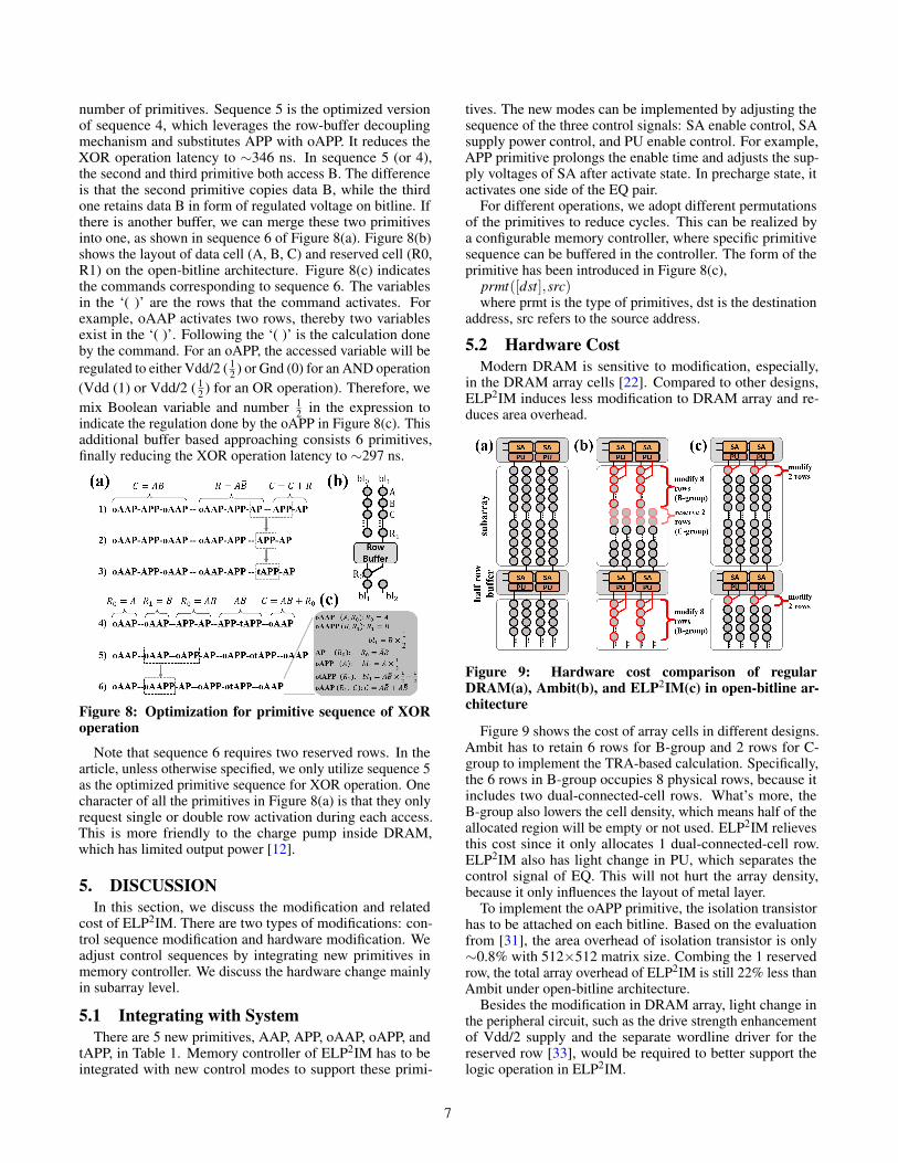
5.2 Hardware CostModern DRAM is sensitive to modification, especially,
in the DRAM array cells [22]. Compared to other designs,ELP2IM induces less modification to DRAM array and re-duces area overhead.
Figure 9: Hardware cost comparison of regularDRAM(a), Ambit(b), and ELP2IM(c) in open-bitline ar-chitecture
Figure 9 shows the cost of array cells in different designs.Ambit has to retain 6 rows for B-group and 2 rows for C-group to implement the TRA-based calculation. Specifically,the 6 rows in B-group occupies 8 physical rows, because itincludes two dual-connected-cell rows. What’s more, theB-group also lowers the cell density, which means half of theallocated region will be empty or not used. ELP2IM relievesthis cost since it only allocates 1 dual-connected-cell row.ELP2IM also has light change in PU, which separates thecontrol signal of EQ. This will not hurt the array density,because it only influences the layout of metal layer.
To implement the oAPP primitive, the isolation transistorhas to be attached on each bitline. Based on the evaluationfrom [31], the area overhead of isolation transistor is only∼0.8% with 512×512 matrix size. Combing the 1 reservedrow, the total array overhead of ELP2IM is still 22% less thanAmbit under open-bitline architecture.
Besides the modification in DRAM array, light change inthe peripheral circuit, such as the drive strength enhancementof Vdd/2 supply and the separate wordline driver for thereserved row [33], would be required to better support thelogic operation in ELP2IM.
7

6. EVALUATIONIn the evaluation of ELP2IM, we first conduct circuit-level
simulation to verify the timing and accuracy of logic opera-tion in ELP2IM. Then we analyze the performance and powerefficiency in basic logic operations. Finally, we implementthree case studies to evaluate the efficiency of ELP2IM in realapplications.
6.1 Circuit-level SimulationWe use H-spice for circuit-level simulation. The parame-
ters are derived from Rambus power model [34, 35], whichincludes information such as circuit capacitances, resistances,and transistor dimensions. The timing of control signals inthe circuit agrees with DDR3-1600.
6.1.1 Timing SimulationIn the simulation, we first analyze the timing of pseudo-
precharge state. As the function of pseudo-precharge is simi-lar to precharge, both intending to charge bitlines (or bitline)to Vdd/2, they are supposed to take the same time. However,based on our simulation, pseudo-precharge actually consumesa longer time. This is because the drive strength of SA is re-duced when the supply (difference between supply voltages)is suppressed. Thankfully, the reduction is not significant,because the transistors in SA, different from the access tran-sistors in DRAM cell, are built with low threshold (Vth) toimprove sense and restore speed. Based on the fact that theVth of transistors in SA is 25∼30% of Vdd [36, 37, 38], thedrive strength of SA with half Vdd supply is reduced by11∼23% in our simulation. On the other hand, the SA withhalf Vdd supply is used in pseudo-precharge state, which onlycharges the bitline. While in activation state, SA with regularsupply is required to charge both bitline and cell capacitor.Subtracting the portion of charging cell capacitors, pseudo-precharge state is 13∼20% shorter than the restore time inactivate state and 20∼30% longer than precharge state.
Figure 10: Waveform of ELP2IM in OR, AND operations
Figure 10 shows the waveform of two APP-AP sequences,which are also critical steps for other complex primitive se-
quences. The first APP-AP executes an OR operation. Inthis operation, ELP2IM accesses the first data during activatestate. The data value can be recognized from the small varia-tion of bitline at the beginning of each activate state. Thenthe pseudo-precharge state is switched on. If bitline is ‘0’,it will be regulated to Vdd/2, otherwise, it will remain ‘1’.The following precharge state does not influence the voltagelevel of bitline, because it only drives the bitline, which isnot shown in the waveform, to Vdd/2. Finally, in the secondactivate, the voltage change will not always follow the smallvariations induced by the second data cell. It actually com-plies with the result of an OR operation. The AND operationis executed in the same way, except ‘1’ will be regulated toVdd/2 in pseudo-precharge state.
6.1.2 Reliability AnalyzingThe reliability of ELP2IM, Ambit, and regular DRAM un-
der different process variations (PV) is studied. The bitlinecoupling effect is also taken into consideration. To conductthe simulation, we first identify the worst case of each device.For ELP2IM, bitlines that are pseudo-precharged to Vdd/2have higher error possibility. For Ambit, inconsistent val-ues in TRA, such as ‘101’ or ‘010’, tend to form a ‘weak1’ or ‘weak 0’ after charge sharing, and possibly make thecalculation failed. The worst case for coupling effect un-der open bitline structure are the data patterns that alternatebetween ‘0’ and ‘1’ in wordline direction [39, 40]. Second,given that PV can be categorized into systematic and ran-dom variations, it is difficult to determine every parameterof the circuit is influenced by which variation [41, 42]. Wecarry out Monte-Carlo simulations in two extreme conditions,where variations are all systematic or all random. Any othercondition is the intermediate case between these two.
Figure 11: Error rate of ELP2IM, Ambit, and regularDRAM
Figure 11 shows the simulation result. ELP2IM exhibitslower error rate, especially under random PV (Figure 11(a)).The higher error rate of Ambit can be ascribe into two aspects.First, TRA approach originally reduces the bitline voltagesensing margin, because mismatch of the triple activated cellscould induce more voltage deviation. Under systematic PV(Figure 11(b)), the triple cells are tend to be identical, andthe error rate is suppressed. Second, the TRA may providedifferent variation scale on bitline, which aggravates the cou-pling effects. For example, a ‘weak 0’ could be driven closeto Vdd/2 by its neighbouring ‘strong 1’s, which are gener-ated by three ‘1’ cells in TRA. In the simulation, the bitlineshared (coupled) capacitor is set to 15% of bitline capaci-tor [40, 43, 44]. ELP2IM can avoid the above problems that
8

Ambit suffers, because it only accesses one cell during thecharge sharing process. On the other hand, even if the bitlinecoupling effect is aggravated in pseudo-precharge state, it canbe avoided by the complementary pseudo-precharge strategyintroduced in section 4.1. In the strategy, ELP2IM regulatesvoltage on bitline, which is physically allocated in a differentsubarray.
Note that error rate of ELP2IM is still higher than regularDRAM. This is reasonable, as any modification could breakthe original balance and induce inaccuracy. The inaccuracy ofELP2IM mainly comes from the mismatch of Vdd/2. Becausepseudo-precharge state may set Vdd/2 on bitline, and thefollowing precharge state will set Vdd/2 on bitline. The twoVdd/2 voltages are charged via different paths, which mayinduce slight mismatch. Therefore, in the design of ELP2IM,it is important to keep the supply voltage nodes at SA and PUequal when delivering Vdd/2.
ELP2IM is also facing the challenge of error correction,which is a common problem faced by all bitwise-operationbased PIMs (no matter using what kind of technologies, suchas SRAM, DRAM, NVM, etc. [6, 45, 46, 47]), because thetraditional error correcting code (ECC) is not compatible withbitwise logic operation. Further extensive research wouldbe needed to tackle this problem. However, even withoutnovel error checking method, bitwise PIM is still a promisingarchitecture for error tolerant scenarios such as approximatecomputing or neural network acceleration.
6.2 Performance and Overhead AnalysisWe implement ELP2IM, Ambit and Drisa_nor in DDR3-
1600 to evaluate the latency and power consumption when car-rying out basic logic operations [14]. Note that DDR3-1600is just an example, other type of DRAM is also compatiblewith the aforementioned designs.
Among the three designs, ELP2IM shows the smallestlatency in almost all the basic operations, as shown in Fig-ure 12(a), which can be attributed to the less commands ittakes. For example, to implement an AND operation, it onlytakes 3 primitives, as indicated in section 3.3, while Ambitrequires 4 primitives. Drisa_nor consumes even longer time,excepting the NOR operation, because it needs to transfer anyother logic to a compound of NOR logic, which induces morecommands. On average, ELP2IM is 1.17× faster than Ambit,and 1.12× than Drisa_nor. Note that ELP2IM does not gainmuch benefit on XOR and XNOR operations, because it onlyhas one reserved row. If there is one more buffer in ELP2IM,the improvement can be 1.23× and 1.16× over Ambit andDrisa_nor.
We estimates power consumption based on spice sim-ulation and the power parameters collected from MicronDDR3 DRAM power datasheet [48]. As the logic opera-tion is conducted inside the subarray, which does not includeread/write process, the background power and activate powerbecome the main part in power consumption. In Figure 12(b),Drisa consumes more power as the additional logic gates andlatches greatly increase background power. For ELP2IM, theactivate power of APP increases by ∼31% compared to theregular AP primitive. For Ambit, the multiple wordlines acti-vation in TRA also increases power, ∼22% for each wordline,which can be attributed to the low power efficiency of charge
pump. Although in Figure 12(b), ELP2IM does not showmuch benefit on power consumption compared to Ambit,only 3% better, it still retains large potential in saving power.As it can include more power-saving primitives, such as AAPand AP, in the calculation. In the following case studies, thepower of ELP2IM is 17%∼27% less than Ambit.
Figure 12: Latency and power of Drisa_nor, Ambit, andELP2IM in complementing basic logic
What’s more, the increased part of power consumption inAmbit is more critical, because it is limited by the powerdelivery network and charge pumps, which have limited ca-pacity to simultaneously drive multi-wordline in differentbanks. Therefore, in consideration of power constraint, thethroughput of Ambit will significantly drop below ELP2IM.
For the area overhead, ELP2IM takes even less change thanAmbit, as discussed in the 5.2. While Drisa_nor modifiesDRAM with 24% area overhead, which is a big challenge forDRAM manufacturing.
To sum up, ELP2IM is the most efficient design in aspectsof latency, power, throughput, and area. Adding logic circuitdirectly in subarray level could improve specific operationin the design of Drisa_nor, but cannot bring general benefitwhen compared to ELP2IM and Ambit.
6.3 Improvement for ApplicationsWe build an in-house simulator to calculate the latency,
throughput, and power consumption of ELP2IM on severalapplications. We configure a regular DRAM module with8 banks. The baselines are Ambit, Drisa_nor, and Kaby-Lake CPU [49]. As shown in case study of Bitmap [50]and Bitweaving [51], we first implement ELP2IM in thelight-modified DRAM designs, whose main purpose is torestore data and thereby is sensitive to reserved space over-head. Therefore, these designs should be close to commodityDRAM, and the power constraint and power efficiency areimportant factors. Secondly, we implement ELP2IM in twoaccelerator designs, where DRAM is built in a application-specific way and performance is the first order consideration.Thereby, we construct ELP2IM with two reserved rows tobuffer more data and reduce processing latency.
6.3.1 Case Study: BitmapBitmap indices [50] can offer fast analytics in specific
applications for databases. Traditionally, the bulk bitwiseoperation occupies a significant time in execution of Bitmapindices. Thereby, the DRAM-based bitwise accelerators arepromising candidates for Bitmap. Here we impose Bitmap onan application which tracks the activities of a large number of
9

users (16 million). The tracking case is to count the numberof users who were active every week for the past w weeks,and the number of male users who were active each of thepast w weeks. The case can be divided into two parts: bulkbitwise operation, which is executed in ELP2IM, and countoperation, which is performed with the help of CPU.
In the case study of Bitmap, we compare ELP2IM with 3Ambit designs which are configured with different reservedspace. The baseline is the throughput of implementing thewhole case in CPU. We first conduct the experiment withoutpower constraint, which means DRAM can activate all 8banks simultaneously (even it is not realistic). Then we seton power constraint to evaluate the performance again.
Figure 13: (a)System throughput improvement offeredby ELP2IM and Ambit with different configurations ofreserved space, (b)ELP2IM and Ambit device perfor-mance, excluding CPU, (c)reserved space
The result is shown in Figure 13, where (a) indicates thewhole system performance, and (b) shows the average per-formance of DRAM device. Figure 13(c) shows the numberof reserved rows in the two designs. We draw three conclu-sions from the experiment. First, by allocating more reservedrows, system performance of Ambit is improved, as shownin Figure 13(a). However, the improvement is not linear withthe increment of reserved rows. The throughput gains a sig-nificant improvement when the number of reserved rows areraised from 4 to 6, but the growth is much slower when re-served rows are increased from 6 to 10. What’s more, we findthat even Ambit is allocated more than 10 reserved rows, itcannot catch up ELP2IM. Second, under condition of powerconstraint, the device throughput of Ambit is greatly reduced,which drops up to ∼83% (Figure 13(b)). ELP2IM is also in-fluenced, because the number of activated banks in the sameactivate window is now decreased to the half, from 8 to 4.However, its device throughput only drops 56%, which isquite close to the ratio of decreased banks, 1/2. Third, evenallocated with different number of reserved rows, the devicethroughput of Ambit (Figure 13(b)) tends to be the same un-der power constraint, implying more reserved space cannotoffer much benefit under such condition.
6.3.2 Case Study: Table ScanTable scan [52] is a common operation in a memory-
based database management system. It sequentially readsthe database and checks the columns for the validity of apredicate of a query. It usually takes many cycles to evaluatesimple predicates. For example, a database query Q1 can be
written as the following:Q1 : SELECT COUNT (∗) FROM R WHERE R.a <C1
where R.a < C1 is a simple LESS THAN predicate. Itinvolves a significant number of comparison and incrementoperations. [51] proposes the BitWeaving method to par-allelize comparisons for multiple words. It permutes eachword to store it in a memory column. Hence, the same bit inmultiple words can be compared with bulk bitwise operation.
In the Table Scan case study, Drisa_nor is studied in thecomparison with ELP2IM and Ambit. Given Table Scanis the databases application, where memory capacity is themajor consideration, ELP2IM, Ambit and Drisa_nor (evenDrisa_nor has much area overhead) are regarded as light-modified designs which are sensitive to the overhead of re-served rows and under the limitation of power constraint. Weuse the same calculation strategy as Bitmap. CPU executesthe count operation in BitWeaving. Ambit, Drisa_nor, orELP2IM implements bulk bitwise operations.
Figure 14: (a)Throughput improvement over our base-line CPU offered by Ambit, Drisa_nor, and ELP2IMfor table scan (b)DRAM device performance, (c)reservedspace
In the evaluation, ELP2IM has the highest throughput, asshown in Figure 14(a), which can be attributed to the smalllatency and high bank-level parallelism. What’s more, theimprovement of ELP2IM grows up quickly with the increasein data width, because in BitWeaving method, the propor-tion of CPU-implemented counting is reduced when datawidth is extended. However, Ambit cannot gain such obviousimprovement because its parallelism is impeded by powerconstraint. Figure 14(b) is the average device performance ofAmbit, Drisa_nor, and ELP2IM, excluding the part of CPU.ELP2IM still maintains the best performance in all the as-pects. Although Drisa_nor is integrated with the high-speedlogic gates near row buffers, its latency is still the largest.However, the throughput of Drisa_nor outperforms Ambit,because Ambit is hindered by the multiple row activates un-der power constraint. Figure 14(c) indicates that Ambit andELP2IM are allocated with 8 rows and 1 row respectively. AsDrisa_nor is attached with additional latches near row buffers,it does not require reserved rows, but in cost of even morearea. In conclusion, ELP2IM consumes the least resource andachieves the best performance.
6.3.3 Case Study: CNNSeveral studies use bitwise operation to accelerate convolu-
10

tional neural network (CNN) applications, such as Dracc [19]and NID [53, 54]. We perform these two designs as casestudies to evaluate the efficiency of our proposed ELP2IM.Given that CNN accelerator is more focused on calculationperformance, it would be acceptable for DRAM to be addedwith more circuit to break the original limitation in DRAM,even though at some cost of density [55, 56]. Thereby, we donot set the limitation of power constraint in the simulation.For ELP2IM, we exploit the sequence 6 in Figure 8 for XORoperation. For Ambit, we allocate a large number of reservedrows, which helps reduce the calculation latency.
Dracc builds in-memory adders by modifying the subarraywith limited number of transistors. Therefore, besides thebitwise operation, Dracc also realizes word-wise addition insubarray level. Leveraging the integrated adder, Dracc canbe applied to the ternary weight neural networks (TWNs),which replaces full precision weights with ternary weights (‘-1’, ‘0’ or ‘+1’). Thereby, it transfers dot product calculationto addition operations [57, 58]. Dracc also proposes severaloperation modes, such as high throughput mode, single framemode, and low power mode, to meet different applicationrequirements.
Table 2: Application in DraccLenet5 Cifar10 Alexnet VGG16 VGG19
Ambit (FPS) 7697.4 6008.4 84.8 4.8 4.1ELP2IM (FPS) 8329.5 6850.5 96.4 5.4 4.6Improvement 1.08× 1.14× 1.14× 1.13× 1.13×Drisa_nor (FPS) 6107.2 3889.7 55.5 3.2 2.7Improvement 0.79× 0.65× 0.66× 0.68× 0.66×
Dracc implements addition based on Ambit approach. Itdivides an addition operation into several basic logic steps,which can also be realized by ELP2IM and Drisa_nor. Inour simulation, we exploit the three designs to realize theadder in Dracc separately. We first optimize the commandsequence to achieve the minimum operation cycles. Then werun TWNs in the high throughput mode of Dracc, which canfully exploit the hardware resources.
Table 2 shows the result of Dracc based on the three ap-proaches. Given that there are only 13 commands (includingtwo new propagation and shift commands, which cannot beoptimized) for the addition operation in Dracc, the spaceleft for optimization is limited. ELP2IM still improves theperformance by 12% (on average). Note that this improve-ment is achieved by the shorter latency of ELP2IM, insteadof higher parallelism, as we have removed the limitation ofpower constraint. In the opposite, Drisa_nor impedes theperformance by 31%. Depending on the proportion of datacomputation and data movement in different neural networks,the improvement (or reduction) changes.
NID realizes binary CNN inside DRAM. It implementsXOR and count operations, which are the dominant calcula-tions in binary CNN [59, 60], by exploiting Ambit approach.To implement the count operation, NID firstly permutes eachword and stores it in column-wise. Then it decomposes thecount operation into minimum number of AND and XORoperations, thereby realizing the count with bulk bitwise oper-ation. NID is embedded with accumulators and comparatorsin peripheral area to assist the processing of other layers, suchas max pooling and normalization.
Table 3: Application in NIDLenet5 Alexnet Resnet18 Resnet34 Resnet50
Ambit (FPS) 7525.1 227.1 9.5 4.7 1.4ELP2IM (FPS) 9958.7 252.6 12.4 6.1 1.7Improvement 1.32 1.11× 1.31× 1.31× 1.25×Drisa_nor (FPS) 5497.1 205.9 7.1 3.5 1.1Improvement 0.73× 0.91× 0.74× 0.74× 0.79×
In our experiment, we apply Ambit, ELP2IM, and Drisa_norto implement the XOR and count operations in NID. Thenwe compare the performance obtained by the three methods,as shown in table 3. On average, ELP2IM achieves 1.26×throughput. This can be attributed to the fact that ELP2IM isinitially faster than Ambit in basic logic operations. Thus it isalso faster in the compound Boolean function. The other im-plicit reason is that ELP2IM is better at optimizing commandsequence, because it contains 6 different primitives, whichmakes the optimization quite flexible. Meanwhile, the countoperation in NID contains a large number of cycles, offeringa wide space for optimization. Therefore, ELP2IM achievessignificant improvement in NID. Drisa_nor is neither fasterthan Ambit in basic operations nor flexible in the optimiza-tion of command sequence. Therefore, it loses performanceby 22% on average.
7. CONCLUSIONIn conclusion, we present ELP2IM, which provides a solid
improvement for bitwise operation using DRAM technology.It retains the benefit and breaks the limitation of state-of-the-art work. It is based on a lightweight pseudo-precharge state,which offers the opportunity to implement in-place operationand improves calculation accuracy.
Benefiting from the mechanism, ELP2IM improves theperformance by reducing the number of primitives and intra-subarray data movement. ELP2IM lowers the power con-sumption by diminishing the number of simultaneously acti-vated rows. Meanwhile, ELP2IM achieves such significantimprovement even with less reserved space, relieving themodification on DRAM.
Our simulation result shows that, in bitmap and table scanapplication, ELP2IM achieves up to 3.2× throughput im-provement in consideration of power constraint. Even with-out the limitation of power constraint, ELP2IM still achievesup to 1.26× throughput in CNN applications.
8. ACKNOWLEDGMENTSThis work is supported in part by US National Science
Foundation #1422331, #1535755, #1617071, #1718080,#1725657, #1910413, The authors thank the anonymousreviewers for their constructive comments.
9. REFERENCES[1] O. Villa, et al., “Scaling the Power Wall: A Path to Exascale,” in SC,
2014.
[2] S. McKee, et al., “Reflections on the Memory Wall,” in CF, 2004.
[3] B. Akin, et al., “Data Reorganization in Memory Using 3D-stackedDRAM,” in ISCA, 2015.
11

[4] H. Asghari-Moghaddam, et al., “Chameleon: Versatile and Practicalnear-DRAM Acceleration Architecture for Large Memory Systems,”in MICRO, 2016.
[5] A. Subramaniyan, et al., “Parallel Automata Processor,” in ISCA,2017.
[6] S. Li, et al., “DRISA: A DRAM-based Reconfigurable In-SituAccelerator,” in MICRO, 2017.
[7] Y. Kim, et al., “Assessing merged DRAM/logic technology,” inINTEGRATION, the VLSI journal, 27, 2, 179-194, 1999.
[8] V. Seshadri, et al., “Ambit: In-memory Accelerator for Bulk BitwiseOperations Using Commodity DRAM Technology,” in MICRO, 2017.
[9] Boroumand, Amirali, et al., “Google workloads for consumer devices:Mitigating data movement bottlenecks,” in ASPLOS, 2018.
[10] D. E. Knuth, et al., “The Art of Computer Programming. Fascicle 1:Bitwise Tricks & Techniques; Binary Decision Diagrams,” 2009.
[11] K. Wu, et al., “Compressing Bitmap Indexes for Faster SearchOperations,” In SSDBM, 2002.
[12] M. Shevgoor, et al., “Quantifying the relationship between the powerdelivery network and architectural policies in a 3D-stacked memorydevice.” in MICRO, 2013.
[13] N. Chatterjee, et al., “Architecting an energy-efficient dram system forgpus,” in HPCA, 2017.
[14] JEDEC. DDR3 SDRAM Standard, JESD79-3D. http://www.jedec.org/sites/default/files/docs/JESD79-3D.pdf, 2009.
[15] P. Nair, et al., “ArchShield: Architectural Framework for AssistingDRAM Scaling by Tolerating High Error Rates,” in ISCA, 2013.
[16] T. Zhang, et al., “Half-DRAM: A High-bandwidth and Low-powerDRAM Architecture from the Rethinking of Fine-grained Activation,”in ISCA, 2014.
[17] K. K. Chang, et al., “Low-cost Inter-linked Subarrays (LISA):Enabling Fast Inter-subarray Data Movement in DRAM.” In HPCA,2016.
[18] V. Seshadri, et al., “RowClone: Fast and Energy-efficient in-DRAMBulk Data Copy and Initialization,” in MICRO, 2013.
[19] Q. Deng, et al., “DrAcc: A DRAM Based Accelerator for AccurateCNN Inference,” in DAC, 2018.
[20] X. Xin, et al., “ROC: DRAM-based Processing with ReducedOperation Cycles,” in DAC, 2019.
[21] T. Zhang, et al., “CREAM: A concurrent-refresh-aware DRAMmemory architecture,” In HPCA, 2014.
[22] S. Lu, et al., “Improving DRAM Latency with Dynamic AsymmetricSubarray,” in MICRO, 2015.
[23] Fl. Krisztián, et al., “Drowsy caches: simple techniques for reducingleakage power,” in Computer Architecture News, 2002.
[24] B. Keeth, et al., “DRAM Circuit Design: Fundamental andHigh-Speed Topics (2nd ed.,” Wiley-IEEE Press, 2007.
[25] P. Salvador, et al., “Exploiting temporal locality in drowsy cachepolicies,” in Proceedings of the 2nd conference on Computingfrontiers, 2005.
[26] F. Brendan, et al., “Drowsy cache partitioning for reduced static anddynamic energy in the cache hierarchy,” in International GreenComputing Conference Proceedings, 2013.
[27] Y. Hamamoto, et al., “Overview and future challenges of floating bodyRAM (FBRAM) technology for 32 nm technology node and beyond,”in Solid-State Electronics journal, 53, 7, 676-683, 2009.
[28] T. Ting, et al., “23.9 An 8-channel 4.5 Gb 180GB/s 18ns-row-latencyRAM for the last level cache,” In ISSCC, 2017.
[29] Y. H. Son, et al., “Reducing memory access latency with asymmetricdram bank organizations,” In ISCA, 2013.
[30] D. Lee, et al., “Tiered-latency DRAM: A Low Latency and Low CostDRAM Architecture,” in HPCA, 2013.
[31] O. Seongil, et al., “Row-buffer Decoupling: A Case for Low-latencyDRAM Microarchitecture,”In ISCA, 2014.
[32] X. Zhang, et al., “Restore truncation for performance improvement infuture DRAM systems,” in HPCA, 2016.
[33] G. Fredeman, et al., “17.4 A 14nm 1.1 Mb embedded DRAM macro
with 1ns access." In ISSCC, 2015.
[34] DRAM Power Model, https://www.rambus.com/energy/, 2010.
[35] T. Vogelsang, et al., “Understanding the Energy Consumption ofDynamic Random Access Memories,” in MICRO, 2010.
[36] H. Kang, et al., “A Sense Amplifier Scheme with Offset Cancellationfor Giga-bit DRAM" Semiconductor Technology and Science journal,7, 2, 67-75, 2007.
[37] S. Chung, et al., “Method and System for DRAM Sensing." US Patent7,369,425, 2008.
[38] T. Na, et al., “Comparative study of various latch-type senseamplifiers." IEEE Transactions on VLSI journal, 22, 2, 425-429, 2013.
[39] S. Seyedzadeh, et al., “Mitigating bitline crosstalk noise in drammemories." In MEMSYS, 2017.
[40] Y. Konishi, et al., “Analysis of coupling noise between adjacent bitlines in megabit DRAMs." Solid-State Circuits journal, 24, 1, 35-42,1989.
[41] B. Zhao, et al., “Process variation-aware nonuniform cachemanagement in a 3D die-stacked multicore processor,” in IEEETransactions on Computers journal, 62, 11, 2252-2265, 2013.
[42] A. Agrawal, et al., “Mosaic: Exploiting the spatial locality of processvariation to reduce refresh energy in on-chip eDRAM modules,” inHPCA, 2014.
[43] Y. Nakagome, et al., “The impact of data-line interference noise onDRAM scaling," Solid-State Circuits journal, 23, 5, 1120-1127, 1988.
[44] J. Liu, et al., “An experimental study of data retention behavior inmodern DRAM devices: Implications for retention time profilingmechanisms," Computer Architecture News journal, 41, 3, 60-71,2013.
[45] C. Eckert, et al., “Neural cache: Bit-serial in-cache acceleration ofdeep neural networks," in ISCA, 2018.
[46] S. Li, et al., “Pinatubo: A Processing-in-Memory Architecture forBulk Bitwise Operations in Emerging Non-volatile Memories," inDAC, 2016.
[47] M. Imani, et al., “FloatPIM: In-Memory Acceleration of Deep NeuralNetwork Training with High Precision," in ISCA, 2019.
[48] Micron, “MT41J256M16HA-125 Data Sheet,”http://www.micron.com/products/dram/.
[49] 7th Generation Intel Core Processor Family for S Platforms, Vol. 1,Datasheet. https://www.intel.com/content/www/us/en/processors/core/7th-gen-core-family-desktop-s-processor-lines-datasheet-vol-1.html.
[50] C. Chan, et al., “Bitmap Index Design and Evaluation,” in SIGMODRec. journal, 27, 2, 355-366, 1998.
[51] Y. Li, et al., “BitWeaving: Fast Scans for Main Memory DataProcessing,” in SIGMOD, 2013.
[52] W. Thomas, et al., “Vectorizing Database Column Scans withComplex Predicates,” in ADMS, 2013.
[53] J. Sim, et al., “NID: Processing Binary Convolutional Neural Networkin Commodity DRAM,” in ICCAD, 2018.
[54] H. Kim, et al., “NAND-Net: Minimizing Computational Complexityof In-Memory Processing for Binary Neural Networks,” in HPCA,2019.
[55] L. Jinag, et al., “XNOR-POP: A processing-in-memory architecturefor binary Convolutional Neural Networks in Wide-IO2 DRAMs,” inISLPED, 2017.
[56] S. Li, et al., “SCOPE: A stochastic computing engine for dram-basedin-situ accelerator,” in MICRO, 2018.
[57] F. Li, et al., “Ternary weight networks.” arXiv preprintarXiv:1605.04711, 2016.
[58] C. Zhu, et al., “Trained ternary quantization.” arXiv preprintarXiv:1612.01064, 2016.
[59] A. Renzo, et al., “YodaNN: An ultra-low power convolutional neuralnetwork accelerator based on binary weights,” in ISVLSI, 2016.
[60] C. Matthieu, et al., “Binaryconnect: Training deep neural networkswith binary weights during propagations,” in NIPS, 2015.
12