em3399 hardware manual · telecom and automotive applications. em3399 is provided with full...
TRANSCRIPT

EM3399 Hardware Manual
V4.201910
www.boardcon.com
Boardcon Embedded Design

1
Customize the embedded system based on Your Idea
1. Introduction
1.1. About this Manual
This manual is intended to provide the user with an overview of the board and benefits, complete
features specifications, and set up procedures. It contains important safety information as well.
1.2. Feedback and Update to this Manual
To help our customers make the most of our products, we are continually making additional and
updated resources available on the Boardcon website (www.boardcon.com , www.armdesigner.com).
These include manuals, application notes, programming examples, and updated software and
hardware. Check in periodically to see what’s new!
When we are prioritizing work on these updated resources, feedback from customers is the number
one influence, If you have questions, comments, or concerns about your product or project, please
no hesitate to contact us at [email protected].
1.3. Limited Warranty
Boardcon warrants this product to be free of defects in material and workmanship for a period of one
year from date of buy. During this warranty period Boardcon will repair or replace the defective unit
in accordance with the following process:
A copy of the original invoice must be included when returning the defective unit to Boardcon. This
limited warranty does not cover damages resulting from lighting or other power surges, misuse,
abuse, abnormal conditions of operation, or attempts to alter or modify the function of the product.
This warranty is limited to the repair or replacement of the defective unit. In no event shall Boardcon
be liable or responsible for any loss or damages, including but not limited to any lost profits, incidental
or consequential damages, loss of business, or anticipatory profits arising from the use or inability
to use this product.
Repairs make after the expiration of the warranty period are subject to a repair charge and the cost
of return shipping. Please contact Boardcon to arrange for any repair service and to obtain repair
charge information.

2
Customize the embedded system based on Your Idea
Content
1 EM3399 Introduction ...................................................................................................................... 3
1.1 Summary .............................................................................................................................. 3
1.2 Rockchip RK3399 Features ................................................................................................. 3
1.3 EM3399 Specifications ......................................................................................................... 4
1.4 PCB Dimension .................................................................................................................... 5
1.5 Block Diagram ...................................................................................................................... 6
1.6 Development Kit Power Meter.............................................................................................. 6
1.7 CPU Introduction .................................................................................................................. 6
2 Peripherals Introduction ............................................................................................................... 18
2.1 Power (P1) ......................................................................................................................... 18
2.2 Audio I/O (J7) ..................................................................................................................... 18
2.3 HDMI IN (J6) ...................................................................................................................... 19
2.4 HDMI OUT (J4) .................................................................................................................. 20
2.5 USB Type-C (J9) ................................................................................................................ 21
2.6 USB HOST (P3, CON9) ..................................................................................................... 22
2.7 Ethernet (JP1) .................................................................................................................... 23
2.8 PCIe x4 (J5) ....................................................................................................................... 24
2.9 eDP Panel (CON3) ............................................................................................................. 25
2.10 MIPI Panel (CON5) .......................................................................................................... 27
2.11 MIPI (CON7, CON8) ......................................................................................................... 27
2.12 Fan (J8) ............................................................................................................................ 29
2.13 Debug (J10) ..................................................................................................................... 30
2.14 GPIO (J2) ......................................................................................................................... 30
2.15 User Buttons (K1, K2, K3) ................................................................................................ 30
2.16 4G Module (CON2, P4) .................................................................................................... 31
2.17 Micro SD (J3) ................................................................................................................... 32
2.18 WiFi&Bluetooth (U10) ...................................................................................................... 33
2.19 RTC (BT1) ........................................................................................................................ 34
3 Product Configurations ................................................................................................................. 35
3.1 Standard Contents ............................................................................................................. 35
3.2 Optional Parts .................................................................................................................... 35

3
Customize the embedded system based on Your Idea
1 EM3399 Introduction
1.1 Summary
The EM3399 is a hexa-core single-board computer based on Rockchip RK3399 processor with two
Cortex A72 cores clocked at up to 1.8GHz, and four Cortex A53 cores teamed with a Mali-T860MP4
GPU, featuring 3G and WiFi/BT module, supporting 4K H.265 video decoding up to 60 fps,
HDMI in/output, USB Type-C, Gigabit Ethernet, and target to 2 in1 Android tablets, VR, TV-BOX,
laptops, in-vehicle navigations, communications and other terminals covering industrial and
consumer applications, including smart Device, advertising devices / all-in-one machines, POS
systems, vehicle control terminals, thin-clients, VOIP video conferencing security / monitoring /
policing, IoT, as well as other fields.
EM3399 is implemented with a PICO3399 computer-on-module providing most of the functions and
interfaces, and EM3399 carrier board providing connectors and several additional functions. The
rich feature set of EM3399 is customizable according to the price / performance needs of the target
application. EM3399 contains expansion connectors which accommodate a wide range of standard
peripheral devices. Wide input range switched power supply is compatible with requirements for
telecom and automotive applications. EM3399 is provided with full ready-to-run Android 7.1.2, Linux
and debian SW packages and comprehensive user manual and designing guide.
1.2 Rockchip RK3399 Features
• Microprocessor
- Dual-core ARM Cortex-A72 up to 1.8G.
- Quad-core ARM Cortex-A53 up to 1.4G.
- 1MB unified L2 Cache for Big cluster, 512KB unified L2 Cache for Little cluster.
• Memory Organization
- On board memory
LPDDR4 up to 8GB.
EMMC5.1 up to 128GB.
- External memory.
SPI NOR
• Cortex-M0
- Two Cortex-M0 cooperate with Cortex-A72/Cortex-A53.
- Integrated sleep modes for low power consumption.
- Serial Wire Debug reduces the number of pins required for debugging.
• PWM
- Four on-chip PWMs with interrupt-based operation.
- Support capture mode and continuous mode or one-shot mode.
• Watchdog
- Three Watchdogs in SoC with 32 bits counter width.
• Interrupt Controller

4
Customize the embedded system based on Your Idea
- Support 8 PPI interrupt source and 148 SPI interrupt sources input.
- Support 16 software-triggered interrupts.
• 3D Graphics Engine
- Arm Mali-T860MP4 GPU up to 4K supply.
- High performance OpenGL ES1.1/2.0/3.0, OpenCL1.2, DirectX11.1 etc.
- Provide MMU and L2 Cache with 256KB size
• Power unit
- RK818 on board.
- Compatible with multiple mode power supply.
- Very low RTC consume current, less 7uA at 3V button Cell.
• Temperature
- Less 46° run video play (exposed board at 20°).
- Less 60° run AnTuTu test (exposed board at 20°)
1.3 EM3399 Specifications
Feature Specifications
CPU Rockchip RK3399. 28nm HKMG process
GPU Mali-T864 GPU
Memory 4GB LPDDR4
Flash 8GB eMMC Flash
Power DC 12V/3A
USB 2x USB2.0 Host, 1x USB3.0 Host, 1x USB Type-C
UART 1x 3pin connector. For debug.
Power in Headphone
HDMI_in
HDMI_out
Type_CDual
USB HostEthernet
WiFi&BT
WiFi antenna
PCIE X4
MIPI_LCD
eDPCamera
MIPI_RXUSB3.0 Host
DebugControl Fun
Reset
PowerRecover
PCIE(SSD/3G/4G)optional
Micro SD
RTC
SIM

5
Customize the embedded system based on Your Idea
LCD 1x eDP LCD via 40-pin header interface, 1x 2-CH MIPI
Ethernet 1000M High performance Ethernet (RTL8211E), RJ45 interface
HDMI IN Adopt Toshiba TC358749XBG bridge device
HDMI OUT HDMI 1.4 /2.0
MIPI Camera 2-CH MIPI RX, Support 3-D video capture
Audio codec Adopt ALC5651 Audio chip, 3.5mm Audio I / O interface
RTC Real Time Clock, powered by external lithium battery
SD card 1x T-Flash card
SIM card 1x SIM card slot
Buttons 3x User Buttons, for Recover, Power, Reset
PCI-E x4 Can be used to connect adapter, such as USB, Network card, Disk array, etc
WIFI&BT AP6356S Module. 2.4/5G WiFi, Bluetooth 4.1
3G/4G PCI-E connector. Shared interface with SSD.
SSD PCI-E connector. Shared interface with 3G/4G.
GPIO 5 groups of GPIO (GPIO0~GPIO4), total 122 GPIOs
Dimension 100mm x 145mm
1.4 PCB Dimension

6
Customize the embedded system based on Your Idea
1.5 Block Diagram
1.6 Development Kit Power Meter
Power OS
Operation
Temperature
°C
Connected Devices
Electric
Current
(mA)
12V/3A Android7.1.2 Room
Temperature
Power, debug port 240
Power, debug port, 10.1’’ MIPI LCD 480
Power, debug port, 10.1’’ MIPI LCD, ethernet, U-
disk, mouse, SD card, HDMI, WiFi&Bluetooth,
4G, Play 4k video
900
1.7 CPU Introduction
The CPU module PICO3399 features 4GB LPDDR4 RAM and 8GB eMMC Flash. MXM3.0-314P
card edge interface.
PICO3399 specifications
Pin number – (P)156+(S)158 = 314 pins
Dimension – 50mm x 82mm
Layer – 8 Layers, complying with EMS/EMI
Power supply – DC 5V or 3.7V Battery
Interface connection: MXM3.0-314P card edge interface
EM3399 CPU Board RK3399 Dual core Cortex-A72 @1.8GHz
Qual core Cortex-A53 @1.4GHz
10-pin header
eDP MIPI_TX MIPI_RX MIPI_RX/TX GPIO ADkey_in
Power_key
RG
MII P
HY
UART2Dual
channelLPDDR3/ LPDDR4
4GB2x32bits
8GB eMMCup to 32GB
HDMI1.4/2.0
PCIE x 4
UART0I2C
I2S
Power (Jack)DC 12V/3A
26-pinheader
8-pin connector
Recover
USB3.0 Type-C USB Host2.0 NET0 SDMMC v3.0 SDIO v3.0
MINI PCIE(3G/SATA SSD) Dual-USB 1000M RJ45
Micro SD WIFI
3-pin connector (Debug)
*
HDMI
StandardPCIe x4
Audio I/O
Multiplexing signal for Camera or HDMI IN.
*
40-pin header
eDP panel
MIPIpanel Camera1 HDMI inor
Camera2
26-pin header
26-pin header
HDMI
Reset_key
RTC
Bluetooth
Gl8506ASM1153E
Type-C
GPIO2-pin connector ( )Fan

7
Customize the embedded system based on Your Idea
Application – smart Device, advertising devices, all-in-one machines, POS systems, vehicle control
terminals, etc.
Mechanical Specification
B2B Connector Specification
MXM 3.0 314Pin Foxconn AS0B821-S43B-7H connector

8
Customize the embedded system based on Your Idea
Pin Definition
Pin Signal Function Description / Alternate
functions
IO
Level
P1 VCC_SYS Main Power Input 3.4-5.5V Wide power input P
P2 VCC_SYS Main Power Input 3.4-5.5V Wide power input P
P3 VCC_SYS Main Power Input 3.4-5.5V Wide power input P
P4 VCC_SYS Main Power Input 3.4-5.5V Wide power input P
P5 AC_DET EXT-AC detection in Auto power on if connect P1 3.3-
5.5V
P6 PMIC_EXT_EN EXT-DCDC enable To keep Peripheral turn on same
time O
P7 I2C1_SCL I2C1 Bus Clock GPIO4_A2 1.8V
P8 I2C1_SDA I2C1 Bus Data GPIO4_A1 1.8V
P9 I2S1_LRCK_RX I2S1 LRCK input GPIO4_A4_D 1.8V
P10 I2S1_SDO0 I2S1 Data0 output GPIO4_A7_D 1.8V
P11 I2S0_SDO0 I2S0 Data0 output GPIO3_D7_D 1.8V
P12 I2S0_SDO1 I2S0 Data1 output GPIO3_D6_D 1.8V
P13 I2S1_LRCK_TX I2S1 LRCK output GPIO4_A5_D 1.8V
P14 I2S0_LRCK_TX I2S0 LRCK output GPIO3_D2_D 1.8V
P15 3V_GPIO4_C5 GPIO 3V_GPIO4_C5_D 3.0V
P16 I2S0_SDI0 I2S0 Data0 input GPIO3_D3_D 1.8V
P17 3V3_UART2_RX Debug UART RXD GPIO4_C3_U 3.3V
P18 I2C_SCL_HDMI I2C clock line for HDMI GPIO4_C1_U 3.0V
P19 3V_GPIO4_D3 GPIO 3V_GPIO4_D3_D 3.0V
P20 TOUCH_RST_L Touch screen reset GPIO4_C6_D 3.0V
P21 3V_GPIO4_D1 GPIO 3V_GPIO4_D1_D 3.0V

9
Customize the embedded system based on Your Idea
P22 BT_WAKE_L BT wake CPU in GPIO2_D2_U or SDIO0
detection 1.8V
P23 SDIO0_D1 WIFI SDIO D1 GPIO2_C5_U or SPI5_TXD 1.8V
P24 UART0_RXD UART receive data GPIO2_C0_U 1.8V
P25 UART0_RTS UART ready-to-send GPIO2_C3_U 1.8V
P26 UART0_CTS UART clear to send GPIO2_C2_U 1.8V
P27 GND Ground 0V
P28 MIPI_TX/RX_D0P MIPI DSI or CSI MIPI_TX1/RX1_D0P 1.8V
P29 MIPI_TX/RX_D0N MIPI DSI or CSI MIPI_TX1/RX1_D0N 1.8V
P30 GND Ground 0V
P31 MIPI_TX/RX_D1P MIPI DSI or CSI TX1/RX1_D1P 1.8V
P32 MIPI_TX/RX_D1N MIPI DSI or CSI TX1/RX1_D1N 1.8V
P33 GND Ground 0V
P34 MIPI_TX/RX_CLK
P MIPI DSI or CSI TX1/RX1_CLKP 1.8V
P35 MIPI_TX/RX_CLK
N MIPI DSI or CSI TX1/RX1_CLKN 1.8V
P36 GND Ground 0V
P37 MIPI_TX/RX_D2P MIPI DSI or CSI TX1/RX1_D2P 1.8V
P38 MIPI_TX/RX_D2N MIPI DSI or CSI TX1/RX1_D2N 1.8V
P39 GND Ground 0V
P40 MIPI_TX/RX_D3P MIPI DSI or CSI TX1/RX1_D3P 1.8V
P41 MIPI_TX/RX_D3N MIPI DSI or CSI TX1/RX1_D3N 1.8V
P42 GND Ground 0V
P43 MIPI_RX_D3P MIPI CSI RX0_D3P 1.8V
P44 MIPI_RX_D3N MIPI CSI RX0_D3N 1.8V
P45 GND Ground 0V
P46 MIPI_RX_D2P MIPI CSI RX0_D2P 1.8V
P47 MIPI_RX_D2N MIPI CSI RX0_D2N 1.8V
P48 GND Ground 0V
P49 MIPI_RX_CLKP MIPI CSI MIPI_RX0_CLKP 1.8V
P50 MIPI_RX_CLKN MIPI CSI MIPI_RX0_CLKP 1.8V
P51 GND Ground 0V
P52 MIPI_RX_D1P MIPI CSI MIPI_RX0_D1P 1.8V
P53 MIPI_RX_D1N MIPI CSI MIPI_RX0_D1N 1.8V
P54 GND Ground 0V
P55 MIPI_RX_D0P MIPI CSI MIPI_RX0_D0P 1.8V
P56 MIPI_RX_D0N MIPI CSI MIPI_RX0_D0P 1.8V
P57 GND Ground 0V
P58 TX_C- HDMI TMDS Clock- HDMI_TCN 1.8V
P59 TX_C+ HDMI TMDS Clock+ HDMI_TCP 1.8V
P60 GND Ground 0V
P61 TX_0- HDMI TMDS Data0- HDMI_TX0N 1.8V

10
Customize the embedded system based on Your Idea
P62 TX_0+ HDM TMDS Data0+ HDMI_TX0P 1.8V
P63 GND Ground 0V
P64 TX_1- HDMI TMDS Data1- HDMI_TX1N 1.8V
P65 TX_1+ HDMI TMDS Data1+ HDMI_TX1P 1.8V
P66 GND Ground 0V
P67 TX_2- HDMI TMDS Data2- HDMI_TX2N 1.8V
P68 TX_2+ HDMI TMDS Data2+ HDMI_TX2P 1.8V
P69 GND Ground 0V
P70 TYPEC0_RX1N Receiver serial data - 1.8V
P71 TYPEC0_RX1P Receiver serial data+ 1.8V
P72 GND Ground 0V
P73 TYPEC0_TX1P Transmitter serial data + 1.8V
P74 TYPEC0_TX1N Transmitter serial data - 1.8V
P75 TYPEC0_RX2N Receiver serial data - 1.8V
P76 TYPEC0_RX2P Receiver serial data+ 1.8V
P77 GND Ground 0V
P78 TYPEC0_TX2P Transmitter serial data + 1.8V
P79 TYPEC0_TX2N Transmitter serial data - 1.8V
P80 GND Ground 0V
P81 TYPEC1_RX1N Receiver serial data - 1.8V
P82 TYPEC1_RX1P Receiver serial data+ 1.8V
P83 GND Ground 0V
P84 TYPEC1_TX1P Transmitter serial data + 1.8V
P85 TYPEC1_TX1N Transmitter serial data - 1.8V
P86 GND Ground 0V
P87 TYPEC1_RX2N Receiver serial data - 1.8V
P88 TYPEC1_RX2P Receiver serial data+ 1.8V
P89 GND Ground 0V
P90 TYPEC1_TX2P Transmitter serial data + 1.8V
P91 TYPEC1_TX2N Transmitter serial data - 1.8V
P92 GND Ground 0V
P93 TYPEC1_AUXM AUX differential Tx serial
data 1.8V
P94 TYPEC1_AUXP AUX differential Rx serial
data 1.8V
P95 GND Ground 0V
P96 PCIE_RX1_P PCIe differential data
input signal + 1.8V
P97 PCIE_RX1_N PCIe differential data
input signal - 1.8V
P98 GND Ground 0V
P99 PCIE_TX1P PCIe differential data
output signal + 1.8V

11
Customize the embedded system based on Your Idea
P100 PCIE_TX1N PCIe differential data
output signal - 1.8V
P101 GND Ground 0V
P102 PCIE_RX0_P PCIe differential data
input signal + 1.8V
P103 PCIE_RX0_N PCIe differential data
input signal - 1.8V
P104 GND Ground 0V
P105 PCIE_TX0P PCIe differential data
output signal + 1.8V
P106 PCIE_TX0N PCIe differential data
output signal - 1.8V
P107 GND Ground 0V
P108 PCIE_REF_CLKN Reference clock - PCIE_RCLK_100M_N 1.8V
P109 PCIE_REF_CLKP Reference clock + PCIE_RCLK_100M_P 1.8V
P110 GND Ground 0V
P111 HOST0_DP USB host 0 data + 1.8V
P112 HOST0_DM USB host 0 data - 1.8V
P113 GND Ground 0V
P114 HOST1_DP USB host 1 data + 1.8V
P115 HOST1_DM USB host 1 data - 1.8V
P116 GND Ground 0V
P117 GND Ground 0V
P118 WIFI_REG_ON_H WIFI Regulators power
EN GPIO0_B2_d 1.8V
P119 WIFI_HOST_WAK
E_L WIFI to wake-up HOST GPIO0_A3/SDIO0_WRPT_d 1.8V
P120 GPIO0_B3 GPIO 1.8V
P121 GPIO1_A1 GPIO
ISP0_SHUTTER_TRIG/ISP1_
SHUTTER_TRIG/TCPD_CC0_
VCONN_EN_d
1.8V
P122 SPI1_TXD SPI serial data output GPIO1_B0/SPI1_TXD/UART4_
TX_u 1.8V
P123 I2C4_SDA I2C data line GPIO1_B3 1.8V
P124 I2C4_SCL I2C serial clock line GPIO1_B4 1.8V
P125 3V3_GPIO3_B2 GPIO3_B2_u MAC_RXER/I2C5_SDA 3.3V
P126 GND Ground 0V
P127 CIF_CLKOUT Camera main clock output GPIO2_B3/SPI2_CLK/VOP_D
En 1.8V
P128 GND Ground 0V
P129 CIF_D2 Camera interface input
pixel data GPIO2_A2/VOP_D2 1.8V
P130 CIF_D5 Camera interface input GPIO2_A5/VOP_D5 1.8V

12
Customize the embedded system based on Your Idea
pixel data
P131 CIF_D3 Camera interface input
pixel data GPIO2_A3/VOP_D3 1.8V
P132 CIF_D4 Camera interface input
pixel data GPIO2_A4/VOP_D4 1.8V
P133 CIF_D6 Camera interface input
pixel data GPIO2_A6/VOP_D6 1.8V
P134 GND Ground 0V
P135 I2C2_SDA I2C data line GPIO2_A0/VOP_D0/CIF_D0 1.8V
P136 I2C7_SDA I2C data line GPIO2_A7/VOP_D7/CIF_D7 1.8V
P137 CIF_PDN0 CIF power ON/OFF GPIO2_B4/SPI2_CSn0_u 1.8V
P138 GND Ground 0V
P139 GND Ground 0V
P140 eDP_TX3P eDP data lane positive
output 1.8V
P141 eDP_TX3N eDP data lane negative
output 1.8V
P142 GND Ground 0V
P143 eDP_TX2P eDP data lane positive
output 1.8V
P144 eDP_TX2N eDP data lane negative
output 1.8V
P145 GND Ground 0V
P146 NC Not connect /
P147 NC Not connect /
P148 eDP_TX1P eDP data lane positive
output 1.8V
P149 eDP_TX1N eDP data lane negative
output 1.8V
P150 GND Ground 0V
P151 eDP_TX0P eDP data lane positive
output 1.8V
P152 eDP_TX0N eDP data lane negative
output 1.8V
P153 GND Ground 0V
P154 eDP_AXUP eDP CH-AUX positive
differential output 1.8V
P155 eDP_AXUN eDP CH-AUX negative
differential output 1.8V
P156 GND Ground 0V
S1 VCC_SYS Main Power Input 3.4-5.5V Wide power input P
S2 VCC_SYS Main Power Input 3.4-5.5V Wide power input P
S3 VCC_SYS Main Power Input 3.4-5.5V Wide power input P

13
Customize the embedded system based on Your Idea
S4 VCC_SYS Main Power Input 3.4-5.5V Wide power input P
S5 VBuck RTC Power Input If not need, Can NC it. 3.0V
S6 GND Ground 0V
S7 RTC_CLKO_WIFI RTC CLK Output for WIFI 32.768KHz 1.8V
S8 GND Ground 0V
S9 POWER_KEY Key input Single function 5V
S10 Reset_KEY Key input Single function 5V
S11 Reset_OUT Main Reset Out NC /
S12 I2S0_SDO3 I2S serial data output GPIO3_D4 1.8V
S13 I2S0_SCLK I2S serial clock GPIO3_D0 1.8V
S14 I2C1_SCLK I2SC serial clock GPIO4_A3 1.8V
S15 I2S1_SDI0 I2S serial data input GPIO4_A6 1.8V
S16 I2S0_SDO2 I2S serial data output GPIO3_D5_d
/I2S0_SDI2SDO2 1.8V
S17 LCD_BL_PWM Backlight PWM output GPIO4_C2/PWM0/VOP0_PW
M/VOP1_PWM_d 3.0V
S18 I2S0_LRCK_RX Left & right channel signal
for receiving serial data GPIO3_D1 1.8V
S19 3V_GPIO4_D0 GPIO4_D0_U PCIE_CLKREQnB 3.0V
S20 PCIE_PRSNT GPIO4_D6_d 3.0V
S21 3V_GPIO4_D2 GPIO GPIO4_D2_d 3.0V
S22 GND Ground 0V
S23 I2S_CLK I2S clock GPIO4_A0 1.8V
S24 GND Ground 0V
S25 PCIE_PRSNT1# GPIO4_D5_d 3.0V
S26 3V3_UART2_TX UART serial data output 3.3V
S27 3V_GPIO4_D4 GPIO GPIO4_D4_d 3.0V
S28 I2C_SDA_HDMI I2C data line for HDMI GPIO4_C0_u 3.0V
S29 HDMI_CEC HDMI CEC signal GPIO4_C7/EDP_HOTPLUG_u 3.0V
S30 GND Ground 0V
S31 SDIO0_CLK SDIO card clock GPIO2_D1_u 1.8V
S32 GND Ground 0V
S33 HDMI_HPD HDMI hot plug detect
input 3.3V
S34 GPIO2_D3 GIPO SDIO0_PWREN_d 1.8V
S35 GPIO2_D4 GPIO SDIO0_BKPWR_d 1.8V
S36 SDIO0_CMD WIFI SDIO command
output and response input GPIO2_D0_u 1.8V
S37 SDIO0_D2 WIFI SDIO D2 GPIO2_C6/SPI5_CLK_u 1.8V
S38 SDIO0_D3 WIFI SDIO D3 GPIO2_C7/SPI5_CSn0_u 1.8V
S39 UART0_TXD UART serial data output GPIO2_C1_u 1.8V
S40 SDIO0_D0 WIFI SDIO D0 GPIO2_C4/SPI5_RXD_u 1.8V
S41 GND Ground 0V

14
Customize the embedded system based on Your Idea
S42 MIPI_TX_D3N MIPI DSI 1.8V
S43 MIPI_TX_D3P MIPI DSI 1.8V
S44 GND Ground 0V
S45 MIPI_TX_D2N MIPI DSI 1.8V
S46 MIPI_TX_D2P MIPI DSI 1.8V
S47 GND Ground 0V
S48 MIPI_TX_CLKN MIPI DSI Clock - 1.8V
S49 MIPI_TX_CLKP MIPI DSI Clock + 1.8V
S50 GND Ground 0V
S51 MIPI_TX_D1N MIPI DSI 1.8V
S52 MIPI_TX_D1P MIPI DSI 1.8V
S53 GND Ground 0V
S54 MIPI_TX_D0N MIPI DSI 1.8V
S55 MIPI_TX_D0P MIPI DSI 1.8V
S56 GND Ground 0V
S57 GND Ground 0V
S58 VCC3V3_SYS VCC_IO Output For Peripheral used 3.3V
S59 VCC3V3_SYS VCC_IO Output For Peripheral used 3.3V
S60 VCC3V3_SYS VCC_IO Output For Peripheral used 3.3V
S61 VCC_EFUSE eFuse program and sense
power input If not need, Can NC it. 1.8V
S62 VCC_EFUSE eFuse program and sense
power input If not need, Can NC it. 1.8V
S63 GND Ground 0V
S64 TYPEC0_AUXM AUX differential Tx serial
data 1.8V
S65 TYPEC0_AUXP AUX differential Rx serial
data 1.8V
S66 GND Ground 0V
S67 TYPEC0_CC1 Configuration Channel1 NC it /
S68 GND Ground 0V
S69 TYPEC0_RCLKP External reference clock NC it 1.8V
S70 TYPEC0_RCLKN External reference clock NC it 1.8V
S71 GND Ground 0V
S72 TYPEC0_CC2 Configuration Channel2 NC it /
S73 GND Ground 0V
S74 TYPEC0_DP USB 2.0 data DP 1.8V
S75 TYPEC0_DM USB 2.0 data DN 1.8V
S76 TYPEC1_DM USB 2.0 data DN 1.8V
S77 TYPEC1_DP USB 2.0 data DP 1.8V
S78 GND Ground 0V
S79 ADKEY_IN 10bit ADC input signal ADC_IN1 1.8V
S80 ADC_IN2 10bit ADC input signal Need pull high. 1.8V

15
Customize the embedded system based on Your Idea
S81 ADC_IN3 10bit ADC input signal Need pull high. 1.8V
S82 GND Ground 0V
S83 TYPEC0_ID USB 2.0 OTG ID detection Input 3.3V
S84 TYPEC0_U2VBUS
DET
VBUS BUMP into the PHY
for VBUS monitor TYPEC0 Vbus Input 3.3V
S85 GND Ground 0V
S86 PCIE_RX3_N PCIe differential data
input 1.8V
S87 PCIE_RX3_P PCIe differential data
input 1.8V
S88 GND Ground 0V
S89 PCIE_TX3P PCIe differential data
output 1.8V
S90 PCIE_TX3N PCIe differential data
output 1.8V
S91 GND Ground 0V
S92 PCIE_RX2_N PCIe differential data
input signals 1.8V
S93 PCIE_RX2_P PCIe differential data
input 1.8V
S94 GND Ground 0V
S95 PCIE_TX2P PCIe differential data
output 1.8V
S96 PCIE_TX2N PCIe differential data
output 1.8V
S97 GND Ground 0V
S98 BT_HOST_WAKE
_L
Bluetooth device to wake-
up HOST GPIO0_A4/SDIO0_INTn_d 1.8V
S99 SDMMC_D2 SDMMC card data input
and output GPIO4_B2/APJTAG_TCK_u 3.0V
S100 SDMMC_D0 SDMM card data input
and output GPIO4_B0/UART2A_RX_u 3.0V
S101 SDMMC_D1 SDMMC card data input
and output GPIO4_B1/UART2A_TX_u 3.0V
S102 SDMMC_CMD SDMMC card command
output and response input GPIO4_B5/MCUJTAG_TMS_u 3.0V
S103 SDMMC0_DET_L SDMMC card detect GPIO0_A7_u 1.8V
S104 GND Ground 0V
S105 SDMMC_CLK SDMMC card clock GPIO4_B4/MUCJTAG_TCK_d 3.0V
S106 GND Ground 0V
S107 BT_REG_ON_H Regulators power
enable/disable
GPIO0_B1/PMUIO2_VOLSEL_
d 1.8V
S108 SDMMC_D3 SDMMC card data input GPIO4_B3/APJTAG_TMS_u 3.0V

16
Customize the embedded system based on Your Idea
and output
S109 GPIO0_B0 GPIO SDMMC0_WRPT/TEST_CLKO
UT2_u 1.8V
S110 GPIO0_B5 GPIO TCPD_VBUS_FDIS/TCPD_VB
US_SOURCE3_d 1.8V
S111 GPIO1_A4 GPIO ISP0_PRELIGHT_TRIG/ISP1_
PRELIGHT_TRIG_d 1.8V
S112 GPIO1_A2 GPIO
ISP0_FLASHTRIGIN/ISP1_FL
ASHTRIGIN/TCPD_CC1_VCO
NN_EN_d
1.8V
S113 GPIO1_A0 GPIO
ISP0_SHUTTER_EN/ISP1_SH
UTTER_EN/TCPD_VBUS_SIN
K_EN_d
1.8V
S114 GPIO0_A6 GPIO PWM3A_IR_d 1.8V
S115 GPIO1_A3 GPIO ISP0_FLASHTRIGOUT/ISP1_
FLASHTRIGOUT_d 1.8V
S116 SDMMC0_PWR_H GPIO0_A1/DDRIO_PWROFF/
TCPD_CCDB_EN_u 1.8V
S117 GND Ground 0V
S118 SPI1_CLK SPI serial clock GPIO1_B1/PMCU_JTAG_TCK
_u 1.8V
S119 SPI1_CSn0 SPI first chip select signal GPIO1_B2/PMCU_JTAG_TMS
_u 1.8V
S120 PCIE_PERST# Hot plug detect GPIO1_C2/SPI3_CSn0_u 1.8V
S121 PCIE_WAKE# Link Reactivation GPIO1_B5_d 1.8V
S122 GND Ground 0V
S123 RK3399_26M_OU
T Cannot use for WIFI GPIO0_A2_d 1.8V
S124 GND Ground 0V
S125 SPI1_RXD SPI serial data input GPIO1_A7/UART4_RX_u 1.8V
S126 OTP_OUT_H Over temperature signal
out GPIO1_A6/TSADC_INT_z 1.8V
S127 GPIO1_C6 GPIO TCPD_VBUS_SOURCE0_d 1.8V
S128 GPIO1_D0 GPIO TCPD_VBUS_SOURCE2_d 1.8V
S129 VCCA1V8_CODE
C Codec Power output APIO5_VDDPST Max 300mA 1.8V
S130 GND Ground 0V
S131 GND Ground 0V
S132 I2C2_SCL I2C serial clock line GPIO2_A1/VOP_D1/CIF_D1 1.8V
S133 I2C7_SCL I2C serial clock line GPIO2_B0/VOP_CLK/CIF_VS
YNC 1.8V
S134 I2C6_SDA I2C data line GPIO2_B1/SPI2_RXD/CIF_HR
EF 1.8V

17
Customize the embedded system based on Your Idea
S135 I2C6_SCL I2C serial clock line GPIO2_B2/SPI2_TXD/CIF_CL
KIN 1.8V
S136 GND Ground 0V
S137 GND Ground 0V
S138 SPDIF_TX S/PDIF biphase data
output
GPIO3_C0/MAC_COL/UART3
_CTSn 3.3V
S139 GND Ground 0V
S140 GND Ground 0V
S141 LED0_AD0 Ethernet Link LED PHYAD0 3.3V
S142 LED1_AD1 Ethernet Speed LED PHYAD1 3.3V
S143 LED2_RXDLY Receiver Clock Timing
Control 3.3V
S144 GND Ground 0V
S145 MDI0- 100M/1G Ethernet MDI0- 3.3V
S146 MDI0+ 100M/1G Ethernet MDI0+ 3.3V
S147 GND Ground 0V
S148 NC Not connect /
S149 NC Not connect /
S150 MDI1- 100M/1G Ethernet MDI1- 3.3V
S151 MDI1+ 100M/1G Ethernet MDI1+ 3.3V
S152 GND Ground 0V
S153 MDI2- 100M/1G Ethernet MDI2- 3.3V
S154 MDI2+ 100M/1G Ethernet MDI2+ 3.3V
S155 GND Ground 0V
S156 MDI3- 100M/1G Ethernet MDI3- 3.3V
S157 MDI3+ 100M/1G Ethernet MDI3+ 3.3V
S158 GND Ground 0V

18
Customize the embedded system based on Your Idea
2 Peripherals Introduction
2.1 Power (P1)
The DC JACK is 5.5 x 2.1mm, 3-pin plug Type. Typical 12V/3A DC adapter.
Pin Signal Description Pin Signal Description
1 VDD12V Main power supply.
DC 12V power in 2 GND Ground
3 GND Ground
2.2 Audio I/O (J7)
The EM3399 adopts audio codec ALC5651, provides stereo audio output/input. (PJ327E, 3.5mm
Jack).
Feature
⚫ Low power
⚫ Integrated ADC and DAC
⚫ IIS transfer audio data
⚫ Stereo output, support recording
Pin Signal Description Pin Signal Description
1 GND Ground 2 HPO_R Headphone amplifier
output _Right channel
3 HPO_L Headphone amplifier
output _Left channel 4 PHE_DET Headphone Detect
5 MIC2 Single-end input for microphone
3
14
2
5

19
Customize the embedded system based on Your Idea
2.3 HDMI IN (J6)
Adopt Toshiba TC358749XBG bridge device. Regular 19pins HDMI type A, with width 13.9mm and
thickness 4.45mm.
HDMI-RX Interface Features
⚫ HDMI 1.4b
⚫ Video Formats Support (Up to 1080p @60fps)
⚫ RGB, YCbCr444: 24-bpp @60fps
⚫ YCbCr422 24-bpp @60fps
⚫ Audio Supports
⚫ Internal Audio PLL to track N/CTS value transmitted by the ACR packet
⚫ 3D Support
⚫ HDCP1.4a Support
⚫ EDID Support
⚫ Release A, Revision 1 (Feb 9, 2000)
⚫ First 128 byte (EDID 1.3 structure)
⚫ First E-EDID Extension: 128 bytes of CEA Extension version 3 (specified in CEA-861-D)
⚫ Embedded 1K-byte SRAM (EDID_SRAM)
⚫ Maximum HDMI clock speed: 165 MHz
1
19
HDMI OUT HDMI IN
HDMI OUT
HDMI monitor
Board A Board B

20
Customize the embedded system based on Your Idea
Pin Signal Description Pin Signal Description
1 HDMI_RX2+ HDMI Data 2 channel
positive 2 GND Ground
3 HDMI_RX2- HDMI Data 2 channel
negative 4 HDMI_RX1+
HDMI Data 1 channel
positive
5 GND Ground 6 HDMI_RX1- HDMI Data 1 channel
negative
7 HDMI_RX0+ HDMI Data 0 channel
positive 8 GND Ground
9 HDMI_RX0- HDMI Data 0 channel
negative 10 HDMI_RXC+
HDMI Clock channel
positive
11 GND Ground 12 HDMI_RXC- HDMI Clock channel
negative
13 HDMIIN_CEC CEC signal 14 NC Not connect
15 HDMIIN_DDC_
SCL DDC Slave Clock 16
HDMIIN_DDC_
SDA DDC Slave data
17 GND Ground 18 HDMIIN_5V 5V power supply
19 HDMIIN_HPDO Hot Plug Detect
Output
2.4 HDMI OUT (J4)
EM3399 supports up to 1080p at 120Hz and 4kx2k at 60Hz HDTV display resolutions. Single
Physical Layer PHY with support for HDMI 1.4 and 2.0 operation
For HDMI operation, support for the following
⚫ HPD input analog comparator
⚫ 13.5–600MHz input reference clock
⚫ Up to 10-bit Deep Color modes
⚫ Up to 18Gbps aggregate bandwidth
⚫ Up to 1080p at 120Hz and 4kx2k at 60Hz HDTV display resolutions and up to QXGA graphic
display resolutions
⚫ 3-D video formats
⚫ Link controller flexible interface with 30-, 60- or 120-bit SDR data access
⚫ Support HDCP 1.4/2.2
Pin Signal Description Pin Signal Description
1 TX_2+ HDMI data 2 pair 2 GND Ground
1
19

21
Customize the embedded system based on Your Idea
3 TX_2- 4 TX_1+ HDMI data 1 pair
5 GND Ground 6 TX_1-
7 TX_0+ HDMI data 0 pair
8 GND Ground
9 TX_0- 10 TX_C+ HDMI clock pair
11 GND Ground 12 TX_C-
13 HDMI_CEC Consumer
electronics control 14 NC Not connect
15 HDMI_SCL HDMI serial clock 16 HDMI_SDA HDMI serial data
17 GND Ground 18 HDMI_VCC 5V power supply
19 HDMI_HPD Hot Plug Detect
2.5 USB Type-C (J9)
EM3399 Type-C is a USB3.1 port, it is used to download image and ADB transfer file, or use a
docking station to connect HDMI, USB and ethernet device.
Feature
⚫ Compliant with USB Type-C Specification, revision 1.1
⚫ Compliant with USB Power Delivery Specification, revision 2.0
⚫ Support USB3.0 Type-C and DisplayPort1.3 Alt Mode on USB Type-C
⚫ Up to 5Gbps data rate for USB3.0
⚫ Up to 5.4Gbps (HBR2) data rate for DP1.2, can support 1/2/4 lane mode
Pin Signal Description Pin Signal Description
A1 GND Ground B1 GND Ground
A2 TYPEC0_TX1
P Transmitter serial data + B2 TYPEC0_TX2P Transmitter serial data +
A3 TYPEC0_TX1
N Transmitter serial data - B3 TYPEC0_TX2N Transmitter serial data -
A1
A12
B1 B2
B11
B12
22
Customize the embedded system based on Your Idea
A4 VBUS_TYPEC VBUS BUMP into the
PHY for VBUS monitor B4 VBUS_TYPEC
VBUS BUMP into the
PHY for VBUS monitor
A5 TYPEC_CC1 Channel Configuration B5 TYPEC_CC2 Channel Configuration
A6 TYPEC0_DP USB 2.0 data DP B6 TYPEC0_DP USB 2.0 data DP
A7 TYPEC0_DM USB 2.0 data DN B7 TYPEC0_DM USB 2.0 data DN
A8 TYPEC0_AUX
P
AUX differential Tx serial
data B8 TYPEC0_AUXM
AUX differential Tx
serial data
A9 VBUS_TYPEC VBUS BUMP into the
PHY for VBUS monitor B9 VBUS_TYPEC
VBUS BUMP into the
PHY for VBUS monitor
A10 TYPEC0_RX2
N Receiver serial data - B10 TYPEC0_RX1N Receiver serial data -
A11 TYPEC0_RX2
P Receiver serial data+ B11 TYPEC0_RX1P Receiver serial data+
A12 GND Ground B12 GND Ground
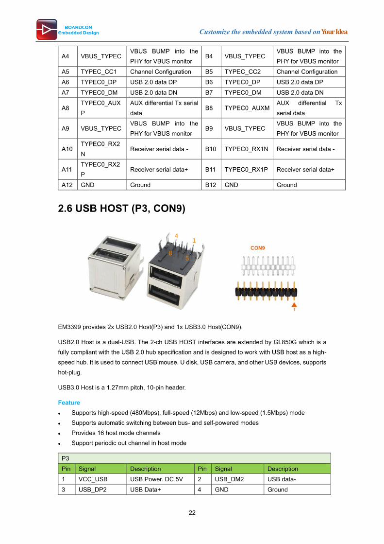
2.6 USB HOST (P3, CON9)
EM3399 provides 2x USB2.0 Host(P3) and 1x USB3.0 Host(CON9).
USB2.0 Host is a dual-USB. The 2-ch USB HOST interfaces are extended by GL850G which is a
fully compliant with the USB 2.0 hub specification and is designed to work with USB host as a high-
speed hub. It is used to connect USB mouse, U disk, USB camera, and other USB devices, supports
hot-plug.
USB3.0 Host is a 1.27mm pitch, 10-pin header.
Feature
⚫ Supports high-speed (480Mbps), full-speed (12Mbps) and low-speed (1.5Mbps) mode
⚫ Supports automatic switching between bus- and self-powered modes
⚫ Provides 16 host mode channels
⚫ Support periodic out channel in host mode
P3
Pin Signal Description Pin Signal Description
1 VCC_USB USB Power. DC 5V 2 USB_DM2 USB data-
3 USB_DP2 USB Data+ 4 GND Ground
1
58
4

23
Customize the embedded system based on Your Idea
5 VCC_USB USB Power. DC 5V 6 USB_DM4 USB data-
7 USB_DP4 USB Data+ 8 GND Ground
CON9
Pin Signal Description Pin Signal Description
1 VDD5V 5V power supply 2 GND Ground
3 TYPEC1_DP USB 2.0 data DP 4 TYPEC1_DM USB 2.0 data DN
5 GND Ground 6 TYPEC1_RX1N Receiver serial data -
7 TYPEC1_RX1P Receiver serial data + 8 GND Ground
9 TYPEC1_TX1N Transmitter serial
data - 10 TYPEC1_TX1P
Transmitter serial
data +
2.7 Ethernet (JP1)
EM3399 adopts RTL8211E as the Ethernet chip. RJ45 connector.
Feature
⚫ Supports 10/100/1000-Mbps data transfer rates with the RGMII interfaces
⚫ Supports both full-duplex and half-duplex operation
⚫ Supports IEEE 802.1Q VLAN tag detection for reception frames
Pin Signal Description Pin Signal Description
1 COM Common 2 MDI0+ Bi-directional
transmit/receive pair 0
3 MDI0- Bi-directional
transmit/receive pair 0 4 MDI1+
Bi-directional
transmit/receive pair 1
5 MDI2+ Bi-directional
transmit/receive pair2 6 MDI2-
Bi-directional
transmit/receive pair2
7 MDI1- Bi-directional
transmit/receive pair 1 8 MDI3+
Bi-directional
transmit/receive pair 3
9 MDI3- Bi-directional
transmit/receive pair 3 10 AGND Ground
11 GLEDA 3.3V 12 GLEDK
(LINK) Detect link
13 YLEDK
(GND) Ground 14
YLEDA
(SPEED) Detect speed
15 GND Ground 16 GND Ground
10 9
12
1112
1314

24
Customize the embedded system based on Your Idea
2.8 PCIe x4 (J5)
The PCIE x4 can be used to connect adapter such as USB, Network card, Disk array, etc.
USB Adapter
Pin Signal Description Pin Signal Description
A1 PCIE_PRSNT
1#
Hot plug presence
detect B1 PCIE_12V 12V power supply
A2 PCIE_12V 12V power supply B2 PCIE_12V 12V power supply
A3 PCIE_12V 12V power supply B3 NC Not connect
A4 GND Ground B4 GND Ground
A5 NC Not connect B5 I2C1_SCL_3V3 SMBus clock
A6 NC Not connect B6 I2C1_SDA_3V3 SMBus data
A7 NC Not connect B7 GND Ground
A8 NC Not connect B8 PCIE_3V3 3.3V power supply
A9 PCIE_3V3 3.3V power supply B9 NC Not connect
A1 A32
B1 B32

25
Customize the embedded system based on Your Idea
A10 PCIE_3V3 3.3V power supply B10 VCC3V3_SYS 3.3V power supply
A11 VCC3V3_SY
S 3.3V power supply B11 PCIE_WAKE# Link Reactivation
A12 GND Ground B12 NC Not connect
A13 PCIE_REF_C
LK_P Reference clock
differential pair
B13 GND Ground
A14 PCIE_REF_C
LK_N B14 PCIE_TX0P Transmit data +
A15 GND Ground B15 PCIE_TX0N Transmit data -
A16 PCIE_RX0_P Receive data + B16 GND Ground
A17 PCIE_RX0_N Receive data - B17 PCIE_PRSNTx
1 Hot plug detect
A18 GND Ground B18 GND Ground
A19 GND Ground B19 PCIE_TX1P Transmit data +
A20 PCIE_RX1_P Receive data + B20 PCIE_TX1N Transmit data -
A21 PCIE_RX1_N Receive data - B21 GND Ground
A22 GND Ground B22 GND Ground
A23 GND Ground B23 PCIE_TX2P Transmit data +
A24 GND Ground B24 PCIE_TX2N Transmit data -
A25 PCIE_RX2_P Receive data + B25 GND Ground
A26 PCIE_RX2_N Receive data - B26 GND Ground
A27 GND Ground B27 PCIE_TX3P Transmit data +
A28 GND Ground B28 PCIE_TX3N Transmit data -
A29 PCIE_RX3_P Receive data + B29 GND Ground
A30 PCIE_RX3_N Receive data - B30 NC Not connect
A31 GND Ground B31 PCIE_PRSNTx
4 Hot plug detect
A32 NC Not connect B32 GND Ground
2.9 eDP Panel (CON3)
EM3399 supports 12.4-inch HD capacitive LCD.
eDP PHY Feature
⚫ Compliant with eDPTM Specification, version 1.3
⚫ Support RGB 6/8/10bit video format
⚫ Up to 4 physical lanes of 2.7/1.62 Gbps/lane
⚫ Support VESA DMT and CVT timing standards
⚫ Fully support EIA/CEA-861Dvideo timing and Info Frame structure
⚫ Hot plug and unplug detection and link status monitor
⚫ Supports Panel Self Refresh (PSR)

26
Customize the embedded system based on Your Idea
Pin Signal Description Pin Signal Description
1 PWIN Power in. 12V power
supply 2 PWIN
Power in. 12V power
supply
3 GND Ground 4 GND Ground
5 VCC3V3_SYS 3.3V power supply 6 VDDIO_18 1.8V power supply
7 GND Ground 8 GND Ground
9 I2C6_SCL I2C serial clock line 10 I2C6_SDA I2C data line
11 TOUCH_RST_L Touch screen reset 12 GPIO3_D4 GPIO
13 3V3_GPIO3_B2 GPIO 14 LCD_BL_PWM Backlight PWM output
15 GND Ground 16 SPDIF_TX S/PDIF biphase data
output
17 ADC_IN2 10bit ADC input
signal 18 ADC_IN3 10bit ADC input signal
19 SPI1_RXD SPI serial data input 20 SPI1_CSn0 SPI first chip select
signal
21 SPI1_CLK SPI serial clock 22 SPI1_TXD SPI serial data output
23 GPIO2_A2 GPIO 24 GPIO2_A3 GPIO
25 GPIO2_A4 GPIO 26 GPIO2_A5 GPIO
27 I2C7_SCL I2C serial clock line 28 I2C7_SDA I2C data line
29 eDP_AXUP eDP CH-AUX positive differential
output
30 eDP_AXUN eDP CH-AUX negative differential
output
31 GND Ground 32 GND Ground
33 EDP_TX3P eDP data lane positive
output
34 EDP_TX3N eDP data lane
negative output
35 EDP_TX2P eDP data lane
positive output 36 EDP_TX2N
eDP data lane
negative output
37 EDP_TX1P eDP data lane
positive output 38 EDP_TX1N
eDP data lane negative
output
39 EDP_TX0P eDP data lane
positive output 40 EDP_TX0N
eDP data lane
negative output
1 3 5 7 9 11 13 15 17 19 21 23 25
2 4 6 8 10 12 14 16 18 20 22 24 26
21 23 25 27 29 31 33 35 37 39
28 30 32 34 36 38 40

27
Customize the embedded system based on Your Idea
2.10 MIPI Panel (CON5)
EM3399 adopts 10.1-inch MIPI panel, resolution 1280 x 800.
Pin Signal Description Pin Signal Description
1 VDD5V 5V power supply 2 VDD5V 5V power supply
3 GND Ground 4 GND Ground
5 VCC3V3_SYS 3.3V power supply 6 VCC3V3_SYS 3.3V power supply
7 VDDIO_18 1.8V power supply 8 GND Ground
9 LCD_BL_PWM Backlight PWM
output 10
3V3_GPIO3_B
2 GPIO
11 SPDIF_TX S/PDIF biphase data
output 12 I2C6_SCL I2C serial clock line
13 I2C6_SDA I2C data line 14 TOUCH_RST_
L Touch screen reset
15 GPIO3_D4 GPIO 16 GND Ground
17 MIPI_TX_D0N
MIPI DSI negative
differential data line
transceiver output
18 MIPI_TX_D0P
MIPI DSI positive
differential data line
transceiver output
19 MIPI_TX_D1N
MIPI DSI negative
differential data line
transceiver output
20 MIPI_TX_D1P
MIPI DSI positive
differential data line
transceiver output
21 MIPI_TX_CLKN
MIPI DSI negative
differential clock line
transceiver output
22 MIPI_TX_CLKP
MIPI DSI positive
differential clock line
transceiver output
23 MIPI_TX_D2N
MIPI DSI negative
differential data line
transceiver output
24 MIPI_TX_D2P
MIPI DSI positive
differential data line
transceiver output
25 MIPI_TX_D3N
MIPI DSI negative
differential data line
transceiver output
26 MIPI_TX_D3P
MIPI DSI positive
differential data line
transceiver output
2.11 MIPI (CON7, CON8)
EM3399 features two 26-pin MIPI connectors.
1 3 5 7 9 11 13 15 17 19 21 23 25
2 4 6 8 10 12 14 16 18 20 22 24 26

28
Customize the embedded system based on Your Idea
Features
⚫ Embedded 3 MIPI PHY, MIPI 0 only for TX use for MIPI LCD, MIPI 1 for TX and RX use for
camera, MIPI 2 only for RX
⚫ Support 4 data lane, providing up to 6Gbps data rate
⚫ Support 1080p@60fps output
⚫ Lane operation ranging from 80 Mbps to 1.5Gbps in forward direction.
CON7
Pin Signal Description Pin Signal Description
1 VDD5V 5V power supply 2 VDD5V 5V power supply
3 GND Ground 4 GND Ground
5 VCC3V3_SYS 3.3V power supply 6 VCC3V3_SYS 3.3V power supply
7 VDDIO_18 1.8V power supply 8 GND Ground
9 GPIO1_A0 GPIO 10 GPIO1_A1 GPIO
11 MIPI_MCLK1 MIPI main clock 1
output 12 I2C2_SCL I2C serial clock line
13 I2C2_SDA I2C data line 14 GPIO1_C6 GPIO
15 GPIO1_D0 GPIO 16 GND Ground
17 MIPI_RX_CLKN
MIPI CSI negative
differential clock line
transceiver output
18 MIPI_RX_CLK
P
MIPI CSI positive
differential clock line
transceiver output
19 MIPI_RX_D0N
MIPI CSI negative
differential data line
transceiver output
20 MIPI_RX_D0P
MIPI CSI positive
differential data line
transceiver output
21 MIPI_RX_D1N
MIPI CSI negative
differential data line
transceiver output
22 MIPI_RX_D1P
MIPI CSI positive
differential data line
transceiver output
23 MIPI_RX_D2N
MIPI CSI negative
differential data line
transceiver output
24 MIPI_RX_D2P
MIPI CSI positive
differential data line
transceiver output
25 MIPI_RX_D3N
MIPI CSI negative
differential data line
transceiver output
26 MIPI_RX_D3P
MIPI CSI positive
differential data line
transceiver output
1 3 5 7 9 11 13 15 17 19 21 23 25
2 4 6 8 10 12 14 16 18 20 22 24 26
1 3 5 7 9 11 13 15 17 19 21 23 25
2 4 6 8 10 12 14 16 18 20 22 24 26

29
Customize the embedded system based on Your Idea
CON8 (Camera)
Pin Signal Description Pin Signal Description
1 VDD5V 5V power supply 2 VDD5V 5V power supply
3 GND Ground 4 GND Ground
5 VCC3V3_SYS 3.3V power supply 6 VCC3V3_SYS 3.3V power supply
7 VDDIO_18 1.8V power supply 8 GND Ground
9 CIF_PDN0 CIF power ON/OFF 10 3V_GPIO4_D0 GPIO
11 MIPI_MCLK0 Camera main clock
0 output 12
I2C4SCL_BCL
K I2C serial clock line
13 I2C4SDA_LRCK I2C data line 14 GPIO3D5_DAC
DAT GPIO
15 GPIO3D6_MCLK GPIO 16 GND Ground
17 MIPI_TX/RX_CL
KN
MIPI CSI negative
differential clock line
transceiver output
18 MIPI_TX/RX_C
LKP
MIPI CSI positive
differential clock line
transceiver output
19 MIPI_TX/RX_D0
N
MIPI CSI negative
differential data line
transceiver output
20 MIPI_TX/RX_D
0P
MIPI CSI positive
differential data line
transceiver output
21 MIPI_TX/RX_D1
N
MIPI CSI negative
differential data line
transceiver output
22 MIPI_TX/RX_D
1P
MIPI CSI positive
differential data line
transceiver output
23 MIPI_TX/RX_D2
N
MIPI CSI negative
differential data line
transceiver output
24 MIPI_TX/RX_D
2P
MIPI CSI positive
differential data line
transceiver output
25 MIPI_TX/RX_D3
N
MIPI CSI negative
differential data line
transceiver output
26 MIPI_TX/RX_D
3P
MIPI CSI positive
differential data line
transceiver output
2.12 Fan (J8)
2-pin connector. It is used to connect the fan to cool down
Pin Signal Description Pin Signal Description
1 GPIO0_A6 GPIO 2 PWIN Power in. 12V power supply
2 1

30
Customize the embedded system based on Your Idea
2.13 Debug (J10)
3-pin connector. The debug serial port baud rate is 1500000.
Pin Signal Description Pin Signal Description
1 UART2DBG_RX UART serial data
input 2
UART2DBG_T
X
UART serial data
output
3 GND Ground
2.14 GPIO (J2)
8-pin connector
Pin Signal Description Pin Signal Description
1 VCC3V3_SYS 3V power supply 2 GND Ground
3 RECOVER/ ADKEY_IN Recover/ AD_in 4 PWR-KEY Power
5 GND Ground 6 IR_IN/ GPIO0_A6 IR_in/GPIO
7 WORK_LED/
GPIO2_D4 LED/GPIO 8
PWR_LED/
GPIO2_D3 LED/GPIO
2.15 User Buttons (K1, K2, K3)
Key Signal Description Key Signal Description
K1 POWER_KEY Power K2 Reset_KEY Reset
K3 RECOVER Recover
3 2 1
8 1

31
Customize the embedded system based on Your Idea
2.16 4G Module (CON2, P4)
EM3399 adopts the standard PCI Express® MiniCard form factor (MiniPCIe) and provides global
network coverage on the connectivity of LTE. It delivers 50Mbps-up and100Mbps-down data rates
on LTE FDD networks and can also be fully backward compatible with existing UMTS and
GSM/GPRS networks.
CON2
Pin Signal Description Pin Signal Description
1 LOUTP Line output + 2 3GVCC DC 3.3V
3 LOUTN Line output - 4 GND Ground
5 MIC1P MIC + 6 NC Not connect
7 MIC1N MIC - 8 SIM_VCC SIM power
9 GND Ground 10 SIM_DATA SIM data
11 NC Not connect 12 SIM_CLK SIM Clock
13 NC Not connect 14 SIM_RST SIM Reset
15 GND Ground 16 NC Not connect
17 NC Not connect 18 GND Ground
19 NC Not connect 20 3GVCC DC 3.3V
21 GND Ground 22 GPIO0_B3 GPIO
23 SATA_TXN/SRX
P SATA data output - 24 3GVCC DC 3.3V
25 SATA_TXP/SRX
N SATA data output + 26 GND Ground
27 GND Ground 28 NC Not connect
29 GND Ground 30 NC Not connect
31 SATA_RXN/STX
N SATA data input - 32 NC Not connect
33 SATA_RXP/STX
P SATA data input + 34 GND Ground
35 GND Ground 36 HOST1_DM Host data DN
37 GND Ground 38 HOST1_DP Host data DP
39 3GVCC DC 3.3V 40 GND Ground
41 3GVCC DC 3.3V 42 LED_WWAN LED
43 GND Ground 44 NC Not connect
45 NC Not connect 46 NC Not connect
1
2
15
52
51
16
17
18

32
Customize the embedded system based on Your Idea
47 NC Not connect 48 NC Not connect
49 NC Not connect 50 GND Ground
51 NC Not connect 52 3GVCC DC 3.3V
The PCIE is share with SSD (mSATA).
P4 is an auto pop-up SIM card slot which is compatible to the standard SIM Card and can be used
for wireless transmission with a 3G/4G module.
SIM Card slot (P4)
Pin Signal Description Pin Signal Description
1 SIM_CLK Clock 2 SIM_DATA send/receiver data
I/O control
3 SIM_RST Reset 4 SIM_VCC Connect to CON5
5 SIM_VCC Connect to CON5 6 GND Ground
7 GND Ground 8 GND Ground
9 GND Ground
2.17 Micro SD (J3)
The Micro SD card is used as an external storage device. The MMC controller interface supports up to 4-
bit transfer modes. MMC is always accessible through the carrier board interface.
9563412
7
8
9
1

33
Customize the embedded system based on Your Idea
Pin Signal Description Pin Signal Description
1 SDMMC_D2 SD/MMC data2 2 SDMMC_D3 SD/MMC data3
3 SDMMC_CMD SD/MMC command
signal 4 VCCIO_SD 3.3V
5 SDMMC_CLK SD/MMC clock 6 GND Ground
7 SDMMC_D0 SD/MMC data0 8 SDMMC_D1 SD/MMC data1
9 SDMMC_DET_L SD/MMC detect signal 10 GND Ground
11 GND Ground 12 GND Ground
2.18 WiFi&Bluetooth (U10)
AP6356S is a low-power consumption module which has incorporated Wi-Fi and Bluetooth into one
chip. The module complies with IEEE 802.11 a/b/g/n/ac standard and it could achieve up to a speed
of 72.2Mbps with single stream in 802.11n draft, 54Mbps as specified in 802.11g, or 11Mbps for
802.11b to connect to the wireless LAN. The integrated module provides SDIO interface for WiFi,
UART / PCM for Bluetooth.
Features
⚫ 802.11a/b/g/n/ac dual-band radio with virtual-simultaneous dual-band operation
⚫ Dual-stream spatial multiplexing up to 867 Mbps data rate.
⚫ Supports 20, 40, 80 MHz channels with optional SGI (256 QAM modulation)
⚫ Supports IEEE 802.11 ac/n beam forming.
⚫ Supports IEEE 802.15.2 external coexistence interface to property
⚫ With other co-located wireless technologies such as LTE, GPS, or WiMAX.
⚫ BT host digital interface:
- HCI UART (up to 4 Mbps)
- PCM for audio data
⚫ Complies with Bluetooth Core Specification Version 4.1 with provisions for supporting
Pin Signal Description Pin Signal Description
1 GND Ground 2 WL/BT_ANT0 WIFI/Buletooth
Antenna
3 GND Ground 4 GND Ground
5 GND Ground 6 GND Ground
7 GND Ground 8 GND Ground
1 11
12
25
2636
50
37
Topview

34
Customize the embedded system based on Your Idea
9 WL_ANT1 WIFI Antenna 10 GND Ground
11 GND Ground 12 NC Not connect
13 XTAL_IN External Crystal in 14 XTAL_OUT External Crystal out
15 WIFI_REG_ON_
H
Low asserting reset
for WiFi core 16
WIFI_HOST_WAK
E_L
WLAN to wake-up
HOST
17 SDIO_CMD SDIO command 18 SDIO_CLK SDIO clock
19 SDIO_D3 SDIO data 20 SDIO_D2 SDIO data
21 SDIO_D0 SDIO data 22 SDIO_D1 SDIO data
23 GND Ground 24 NC Not connect
25 VIN_LDO
Internal Buck
voltage generation
pin
26 VIN_LDO_OUT
Internal Buck
voltage generation
pin
27 BT_PCM_SYNC PCM sync signal 28 BT_PCM_IN PCM data input
29 BT_PCM_OUT PCM Data output 30 BT_PCM_CLK PCM clock
31 RTC_CLKO_WIFI
External Low Power
Clock input
(32.768KHz)
32 GND Ground
33 NC Not connect 34 VDDIO_WL I/O Voltage supply
input
35 NC Not connect 36 VCC_WL
Main power
voltage source
input
37 NC Not connect 38 BT_REG_ON_H
Low asserting
reset for Bluetooth
core
39 GND Ground 40 UART0_RXD Bluetooth UART
interface
41 UART0_TXD Bluetooth UART
interface 42 UART0_CTS
Bluetooth UART
interface
43 UART0_RTS Bluetooth UART
interface 44 NC Not connect
45 NC Not connect 46 NC Not connect
47 NC Not connect 48 NC Not connect
49 BT_WAKE_L HOST wake-up
Bluetooth device 50
BT_HOST_WAKE
_L
Bluetooth device to
wake-up HOST
2.19 RTC (BT1)

35
Customize the embedded system based on Your Idea
The backup battery (3V) is used to ensure the RTC (frequency 32.768KHz) is still able to work after
power off. Lithium cell model: CR1220.
Pin Signal Description Pin Signal Description
1 VBuck 3V battery 2 GND Ground
3 Product Configurations
3.1 Standard Contents
NO. Item Qty. (PCS) Description
1 EM3399 board 1 Standard Content (4GB RAM, 8GB eMMC)
2 CD-ROM 1 Android/Debian BSP, Ubuntu BSP, Documents, tools,
Schematic Drawing, datasheets
3 Ethernet cable 1
4 Serial Cable 1 CP2102
5 USB Cable 1 USB Type-C
6 Power adaptor 1 12V/3A DC
3.2 Optional Parts
• MIPI camera Module (OV13850)
• LCD Module (10.1-inch MIPI panel)
• 4G Module/SSD