embedded peripherals ip user guide
TRANSCRIPT

Embedded Peripherals IP User Guide
SubscribeSend Feedback
UG-01085 | 2017.11.06Latest document on the web: PDF | HTML
Contents
1 Embedded Peripherals IP User Guide Introduction........................................................ 181.1 Tool Support........................................................................................................ 181.2 Device Support.....................................................................................................191.3 Document Revision History.....................................................................................19
2 Avalon-ST Multi-Channel Shared Memory FIFO Core...................................................... 202.1 Core Overview......................................................................................................202.2 Performance and Resource Utilization...................................................................... 202.3 Functional Description........................................................................................... 21
2.3.1 Interfaces................................................................................................ 222.3.2 Operation................................................................................................ 22
2.4 Parameters.......................................................................................................... 232.5 Software Programming Model................................................................................. 24
2.5.1 HAL System Library Support.......................................................................242.5.2 Register Map............................................................................................ 24
2.6 Document Revision History.....................................................................................25
3 Avalon-ST Single-Clock and Dual-Clock FIFO Cores........................................................263.1 Core Overview......................................................................................................263.2 Functional Description........................................................................................... 26
3.2.1 Interfaces................................................................................................ 273.2.2 Operating Modes.......................................................................................273.2.3 Fill Level.................................................................................................. 283.2.4 Thresholds............................................................................................... 28
3.3 Parameters.......................................................................................................... 293.4 Register Description.............................................................................................. 293.5 Document Revision History.....................................................................................30
4 Avalon-ST Serial Peripheral Interface Core.................................................................... 324.1 Core Overview......................................................................................................324.2 Functional Description........................................................................................... 32
4.2.1 Interfaces................................................................................................ 324.2.2 Operation................................................................................................ 334.2.3 Timing.....................................................................................................334.2.4 Limitations...............................................................................................34
4.3 Configuration....................................................................................................... 344.4 Document Revision History.....................................................................................34
5 SPI Core.........................................................................................................................355.1 Core Overview......................................................................................................355.2 Functional Description........................................................................................... 35
5.2.1 Example Configurations............................................................................. 365.2.2 Transmitter Logic...................................................................................... 375.2.3 Receiver Logic.......................................................................................... 375.2.4 Master and Slave Modes............................................................................ 37
5.3 Configuration....................................................................................................... 395.3.1 Master/Slave Settings................................................................................395.3.2 Data Register Settings...............................................................................40
Contents
Embedded Peripherals IP User Guide2

5.3.3 Timing Settings........................................................................................ 405.4 Software Programming Model................................................................................. 41
5.4.1 Hardware Access Routines..........................................................................415.4.2 Software Files...........................................................................................425.4.3 Register Map............................................................................................ 43
5.5 Document Revision History.....................................................................................46
6 Ethernet MDIO Core....................................................................................................... 476.1 Core Overview......................................................................................................476.2 Functional Description........................................................................................... 47
6.2.1 MDIO Frame Format (Clause 45).................................................................486.2.2 MDIO Clock Generation..............................................................................496.2.3 Interfaces................................................................................................ 496.2.4 Operation................................................................................................ 49
6.3 Parameter............................................................................................................496.4 Configuration Registers..........................................................................................506.5 Document Revision History.....................................................................................50
7 Intel FPGA 16550 Compatible UART Core.......................................................................517.1 Core Overview......................................................................................................517.2 Feature Description............................................................................................... 51
7.2.1 Unsupported Features................................................................................527.2.2 Interface................................................................................................. 527.2.3 General Architecture..................................................................................547.2.4 16550 UART General Programming Flow Chart.............................................. 547.2.5 Configuration Parameters...........................................................................567.2.6 DMA Support............................................................................................567.2.7 FPGA Resource Usage................................................................................577.2.8 Timing and Fmax...................................................................................... 577.2.9 Avalon-MM Slave...................................................................................... 587.2.10 Overrun/Underrun Conditions................................................................... 597.2.11 Hardware Auto Flow-Control..................................................................... 607.2.12 Clock and Baud Rate Selection.................................................................. 61
7.3 Software Programming Model................................................................................. 617.3.1 Overview................................................................................................. 617.3.2 Supported Features...................................................................................617.3.3 Unsupported Features................................................................................627.3.4 Configuration........................................................................................... 627.3.5 16550 UART API....................................................................................... 627.3.6 Driver Examples....................................................................................... 66
7.4 Address Map and Register Descriptions ................................................................... 707.4.1 rbr_thr_dll............................................................................................... 717.4.2 ier_dlh.................................................................................................... 727.4.3 iir........................................................................................................... 747.4.4 fcr.......................................................................................................... 757.4.5 lcr...........................................................................................................777.4.6 mcr.........................................................................................................787.4.7 lsr...........................................................................................................797.4.8 msr.........................................................................................................817.4.9 scr..........................................................................................................837.4.10 afr........................................................................................................ 84
Contents
Embedded Peripherals IP User Guide3
7.4.11 tx_low................................................................................................... 857.5 Document Revision History.....................................................................................85
8 UART Core......................................................................................................................878.1 Core Overview......................................................................................................878.2 Functional Description........................................................................................... 87
8.2.1 Avalon-MM Slave Interface and Registers..................................................... 878.2.2 RS-232 Interface...................................................................................... 888.2.3 Transmitter Logic...................................................................................... 888.2.4 Receiver Logic.......................................................................................... 888.2.5 Baud Rate Generation................................................................................89
8.3 Instantiating the Core............................................................................................898.3.1 Configuration Settings............................................................................... 898.3.2 Simulation Settings................................................................................... 92
8.4 Simulation Considerations......................................................................................928.5 Software Programming Model................................................................................. 93
8.5.1 HAL System Library Support.......................................................................938.5.2 Software Files...........................................................................................958.5.3 Register Map............................................................................................ 968.5.4 Interrupt Behavior...................................................................................100
8.6 Document Revision History...................................................................................100
9 Intel FPGA Avalon Mailbox Core...................................................................................1029.1 Core Overview....................................................................................................1029.2 Functional Description..........................................................................................102
9.2.1 Message Sending and Retrieval Process......................................................1039.2.2 Registers of Component........................................................................... 103
9.3 Interface............................................................................................................1059.3.1 Component Interface...............................................................................1059.3.2 Component Parameterization.................................................................... 106
9.4 HAL Driver......................................................................................................... 1079.4.1 Feature Description................................................................................. 107
9.5 Document Revision History...................................................................................112
10 Intel FPGA Avalon Mutex Core................................................................................... 11310.1 Core Overview.................................................................................................. 11310.2 Functional Description........................................................................................11310.3 Configuration....................................................................................................11410.4 Software Programming Model..............................................................................114
10.4.1 Software Files....................................................................................... 11410.4.2 Hardware Access Routines...................................................................... 115
10.5 Mutex API........................................................................................................ 11510.5.1 altera_avalon_mutex_is_mine().............................................................. 11510.5.2 altera_avalon_mutex_first_lock()............................................................ 11610.5.3 altera_avalon_mutex_lock()....................................................................11610.5.4 altera_avalon_mutex_open().................................................................. 11610.5.5 altera_avalon_mutex_trylock()................................................................11710.5.6 altera_avalon_mutex_unlock()................................................................ 117
10.6 Document Revision History................................................................................. 117
11 Intel FPGA Avalon I2C (Master) Core......................................................................... 11811.1 Core Overview.................................................................................................. 118
Contents
Embedded Peripherals IP User Guide4
11.2 Feature Description........................................................................................... 11811.2.1 Supported Features............................................................................... 11811.2.2 Unsupported Features............................................................................ 118
11.3 Configuration Parameters................................................................................... 11811.4 Interface..........................................................................................................11911.5 Registers..........................................................................................................120
11.5.1 Register Memory Map............................................................................ 12011.5.2 Register Descriptions............................................................................. 121
11.6 Reset and Clock Requirements............................................................................ 12511.7 Functional Description........................................................................................125
11.7.1 Overview..............................................................................................12511.7.2 Configuring TFT_CMD Register Examples.................................................. 12611.7.3 I2C Serial Interface Connection............................................................... 12711.7.4 Avalon-MM Slave Interface..................................................................... 12811.7.5 Avalon-ST Interface............................................................................... 12911.7.6 Programming Model...............................................................................129
11.8 Document Revision History................................................................................. 132
12 Intel FPGA I2C Slave to Avalon-MM Master Bridge Core............................................. 13312.1 Core Overview.................................................................................................. 13312.2 Functional Description........................................................................................133
12.2.1 Block Diagram...................................................................................... 13312.2.2 N-byte Addressing................................................................................. 13312.2.3 N-byte Addressing with N-bit Address Stealing.......................................... 13412.2.4 Read Operation..................................................................................... 13512.2.5 Write Operation.....................................................................................13612.2.6 Interacting with Multi-Master.................................................................. 138
12.3 Platform Designer Parameters............................................................................. 13912.4 Signals............................................................................................................ 13912.5 How to Translate the Bridge's I2C Data and I2C I/O Ports to an I2C Interface............. 14112.6 Document Revision History................................................................................. 142
13 Compact Flash Core................................................................................................... 14313.1 Core Overview.................................................................................................. 14313.2 Functional Description........................................................................................14313.3 Required Connections........................................................................................ 14413.4 Software Programming Model..............................................................................145
13.4.1 HAL System Library Support................................................................... 14513.4.2 Software Files....................................................................................... 14513.4.3 Register Maps....................................................................................... 146
13.5 Document Revision History................................................................................. 147
14 EPCS Serial Flash Controller Core...............................................................................14814.1 Core Overview.................................................................................................. 14814.2 Functional Description........................................................................................149
14.2.1 Avalon-MM Slave Interface and Registers..................................................15014.3 Configuration................................................................................................. 15114.4 Software Programming Model..............................................................................151
14.4.1 HAL System Library Support................................................................... 15114.4.2 Software Files....................................................................................... 152
14.5 Document Revision History................................................................................. 152
Contents
Embedded Peripherals IP User Guide5

15 Intel FPGA Serial Flash Controller and Controller II Core...........................................15315.1 Parameters.......................................................................................................153
15.1.1 Configuration Device Types..................................................................... 15315.1.2 I/O Mode..............................................................................................15415.1.3 Chip Selects..........................................................................................15415.1.4 Interface Signals................................................................................... 154
15.2 Registers..........................................................................................................15615.2.1 Register Memory Map............................................................................ 15615.2.2 Register Descriptions............................................................................. 15615.2.3 Valid Sector Combination for Sector Protect and Sector Erase Command.......160
15.3 Nios II Tools Support......................................................................................... 16115.3.1 Booting Nios II from Flash...................................................................... 16115.3.2 Nios II HAL Driver................................................................................. 163
15.4 Intel FPGA Serial Flash Controller II..................................................................... 16415.4.1 Register Memory Map............................................................................ 16415.4.2 Configuration Device Types..................................................................... 164
15.5 Document Revision History................................................................................. 165
16 Intel FPGA Generic QUAD SPI Controller and Controller II Core.................................16616.1 Core Overview.................................................................................................. 16616.2 Functional Description........................................................................................16616.3 Parameters.......................................................................................................166
16.3.1 Configuration Device Types..................................................................... 16716.3.2 I/O Mode..............................................................................................16716.3.3 Chip Selects..........................................................................................16716.3.4 Interface Signals................................................................................... 167
16.4 Registers..........................................................................................................16916.4.1 Register Memory Map............................................................................ 16916.4.2 Register Descriptions............................................................................. 17016.4.3 Valid Sector Combination for Sector Protect and Sector Erase Command.......174
16.5 Nios II Tools Support......................................................................................... 17416.5.1 Booting Nios II from Flash...................................................................... 17516.5.2 Nios II HAL Driver................................................................................. 177
16.6 Intel FPGA Generic QUAD SPI Controller II ...........................................................17716.6.1 Register Memory Map............................................................................ 17716.6.2 Configuration Device Types .................................................................... 178
16.7 Document Revision History................................................................................. 179
17 Interval Timer Core....................................................................................................18017.1 Core Overview.................................................................................................. 18017.2 Functional Description........................................................................................180
17.2.1 Avalon-MM Slave Interface..................................................................... 18117.3 Configuration....................................................................................................181
17.3.1 Timeout Period......................................................................................18117.3.2 Counter Size.........................................................................................18217.3.3 Hardware Options..................................................................................18217.3.4 Configuring the Timer as a Watchdog Timer.............................................. 183
17.4 Software Programming Model..............................................................................18317.4.1 HAL System Library Support................................................................... 18417.4.2 Software Files....................................................................................... 18417.4.3 Register Map.........................................................................................185
Contents
Embedded Peripherals IP User Guide6
17.4.4 Interrupt Behavior.................................................................................18717.5 Document Revision History................................................................................. 187
18 JTAG UART Core......................................................................................................... 18918.1 Core Overview.................................................................................................. 18918.2 Functional Description........................................................................................189
18.2.1 Avalon Slave Interface and Registers........................................................19018.2.2 Read and Write FIFOs............................................................................ 19018.2.3 JTAG Interface...................................................................................... 19018.2.4 Host-Target Connection.......................................................................... 190
18.3 Configuration....................................................................................................19118.3.1 Configuration Page................................................................................ 19118.3.2 Simulation Settings............................................................................... 192
18.4 Hardware Simulation Considerations.................................................................... 19318.5 Software Programming Model..............................................................................193
18.5.1 HAL System Library Support................................................................... 19418.5.2 Software Files....................................................................................... 19618.5.3 Accessing the JTAG UART Core via a Host PC.............................................19618.5.4 Register Map.........................................................................................19618.5.5 Interrupt Behavior.................................................................................198
18.6 Document Revision History................................................................................. 199
19 On-Chip FIFO Memory Core........................................................................................20019.1 Core Overview.................................................................................................. 20019.2 Functional Description........................................................................................200
19.2.1 Avalon-MM Write Slave to Avalon-MM Read Slave.......................................20019.2.2 Avalon-ST Sink to Avalon-ST Source........................................................ 20119.2.3 Avalon-MM Write Slave to Avalon-ST Source..............................................20219.2.4 Avalon-ST Sink to Avalon-MM Read Slave................................................. 20319.2.5 Status Interface.................................................................................... 20419.2.6 Clocking Modes..................................................................................... 204
19.3 Configuration....................................................................................................20419.3.1 FIFO Settings........................................................................................20419.3.2 Interface Parameters............................................................................. 205
19.4 Software Programming Model..............................................................................20619.4.1 HAL System Library Support................................................................... 20619.4.2 Software Files....................................................................................... 206
19.5 Programming with the On-Chip FIFO Memory........................................................20619.5.1 Software Control................................................................................... 20719.5.2 Software Example................................................................................. 209
19.6 On-Chip FIFO Memory API..................................................................................21019.6.1 altera_avalon_fifo_init()......................................................................... 21119.6.2 altera_avalon_fifo_read_status()............................................................. 21119.6.3 altera_avalon_fifo_read_ienable()............................................................21119.6.4 altera_avalon_fifo_read_almostfull()........................................................ 21219.6.5 altera_avalon_fifo_read_almostempty()....................................................21219.6.6 altera_avalon_fifo_read_event()..............................................................21219.6.7 altera_avalon_fifo_read_level()............................................................... 21219.6.8 altera_avalon_fifo_clear_event()............................................................. 21319.6.9 altera_avalon_fifo_write_ienable()...........................................................21319.6.10 altera_avalon_fifo_write_almostfull()......................................................213
Contents
Embedded Peripherals IP User Guide7
19.6.11 altera_avalon_fifo_write_almostempty()................................................. 21419.6.12 altera_avalon_write_fifo().....................................................................21419.6.13 altera_avalon_write_other_info()........................................................... 21419.6.14 altera_avalon_fifo_read_fifo()............................................................... 215
19.7 Document Revision History................................................................................. 215
20 On-Chip Memory (RAM and ROM) Core.......................................................................21620.1 Core Overview.................................................................................................. 21620.2 Component-Level Design for On-Chip Memory.......................................................216
20.2.1 Memory Type........................................................................................ 21720.2.2 Size.....................................................................................................21820.2.3 Read Latency........................................................................................21820.2.4 ROM/RAM Memory Protection..................................................................21820.2.5 ECC Parameter......................................................................................21820.2.6 Memory Initialization............................................................................. 219
20.3 Platform Designer System-Level Design for On-Chip Memory.................................. 21920.4 Simulation for On-Chip Memory...........................................................................21920.5 Intel Quartus Prime Project-Level Design for On-Chip Memory.................................21920.6 Board-Level Design for On-Chip Memory.............................................................. 22020.7 Example Design with On-Chip Memory................................................................. 22020.8 Document Revision History................................................................................. 220
21 Optrex 16207 LCD Controller Core............................................................................. 22121.1 Core Overview.................................................................................................. 22121.2 Functional Description........................................................................................22121.3 Software Programming Model..............................................................................222
21.3.1 HAL System Library Support................................................................... 22221.3.2 Displaying Characters on the LCD............................................................ 22221.3.3 Software Files....................................................................................... 22321.3.4 Register Map.........................................................................................22321.3.5 Interrupt Behavior.................................................................................223
21.4 Document Revision History................................................................................. 224
22 PIO Core.................................................................................................................... 22522.1 Core Overview.................................................................................................. 22522.2 Functional Description........................................................................................225
22.2.1 Data Input and Output........................................................................... 22622.2.2 Edge Capture........................................................................................22622.2.3 IRQ Generation..................................................................................... 226
22.3 Example Configurations......................................................................................22722.3.1 Avalon-MM Interface..............................................................................227
22.4 Configuration....................................................................................................22722.4.1 Basic Settings....................................................................................... 22722.4.2 Input Options........................................................................................22822.4.3 Simulation............................................................................................229
22.5 Software Programming Model..............................................................................22922.5.1 Software Files....................................................................................... 22922.5.2 Register Map.........................................................................................22922.5.3 Interrupt Behavior.................................................................................23122.5.4 Software Files....................................................................................... 231
22.6 Document Revision History................................................................................. 232
Contents
Embedded Peripherals IP User Guide8
23 PLL Cores................................................................................................................... 23323.1 Core Overview.................................................................................................. 23323.2 Functional Description........................................................................................234
23.2.1 ALTPLL IP Core......................................................................................23423.2.2 Clock Outputs....................................................................................... 23423.2.3 PLL Status and Control Signals................................................................ 23523.2.4 System Reset Considerations.................................................................. 235
23.3 Instantiating the Avalon ALTPLL Core................................................................... 23523.4 Instantiating the PLL Core.................................................................................. 23523.5 Hardware Simulation Considerations.................................................................... 23623.6 Register Definitions and Bit List........................................................................... 237
23.6.1 Status Register..................................................................................... 23723.6.2 Control Register.................................................................................... 23723.6.3 Phase Reconfig Control Register.............................................................. 238
23.7 Document Revision History................................................................................. 239
24 DMA Controller Core...................................................................................................24024.1 Core Overview.................................................................................................. 24024.2 Functional Description........................................................................................240
24.2.1 Setting Up DMA Transactions...................................................................24124.2.2 The Master Read and Write Ports............................................................. 24224.2.3 Addressing and Address Incrementing......................................................242
24.3 Parameters.......................................................................................................24324.3.1 DMA Parameters (Basic).........................................................................24324.3.2 Advanced Options..................................................................................244
24.4 Software Programming Model..............................................................................24424.4.1 HAL System Library Support................................................................... 24424.4.2 Software Files....................................................................................... 24524.4.3 Register Map.........................................................................................24624.4.4 Interrupt Behavior.................................................................................249
24.5 Document Revision History................................................................................. 249
25 Modular Scatter-Gather DMA Core..............................................................................25025.1 Core Overview.................................................................................................. 25025.2 Feature Description........................................................................................... 25025.3 mSGDMA Interfaces and Parameters....................................................................252
25.3.1 Interface.............................................................................................. 25225.3.2 mSGDMA Parameter Editor..................................................................... 256
25.4 mSGDMA Descriptors.........................................................................................25625.4.1 Read and Write Address Fields.................................................................25725.4.2 Length Field..........................................................................................25725.4.3 Sequence Number Field..........................................................................25825.4.4 Read and Write Burst Count Fields........................................................... 25825.4.5 Read and Write Stride Fields................................................................... 25825.4.6 Control Field......................................................................................... 258
25.5 Programming Model...........................................................................................26025.5.1 Stop DMA Operation.............................................................................. 26025.5.2 Stop Descriptor Operation...................................................................... 26025.5.3 Recovery from Stopped on Error and Stopped on Early Termination..............260
25.6 Register Map of mSGDMA...................................................................................26125.6.1 Status Register..................................................................................... 261
Contents
Embedded Peripherals IP User Guide9

25.6.2 Control Register.................................................................................... 26225.7 Modular Scatter-Gather DMA Prefetcher Core........................................................ 264
25.7.1 Functional Description............................................................................26425.8 Driver Implementation....................................................................................... 277
25.8.1 alt_msgdma_standard_descriptor_async_transfer......................................27725.8.2 alt_msgdma_extended_descriptor_async_transfer..................................... 27825.8.3 alt_msgdma_descriptor_async_transfer....................................................27925.8.4 alt_msgdma_standard_descriptor_sync_transfer....................................... 28025.8.5 alt_msgdma_extended_descriptor_sync_transfer.......................................28125.8.6 alt_msgdma_descriptor_sync_transfer..................................................... 28225.8.7 alt_msgdma_construct_standard_st_to_mm_descriptor..............................28325.8.8 alt_msgdma_construct_standard_mm_to_st_descriptor..............................28425.8.9 alt_msgdma_construct_standard_mm_to_mm_descriptor...........................28525.8.10 alt_msgdma_construct_standard_descriptor............................................28625.8.11 alt_msgdma_construct_extended_st_to_mm_descriptor........................... 28725.8.12 alt_msgdma_construct_extended_mm_to_st_descriptor........................... 28825.8.13 alt_msgdma_construct_extended_mm_to_mm_descriptor........................ 28925.8.14 alt_msgdma_construct_extended_descriptor........................................... 29025.8.15 alt_msgdma_register_callback...............................................................29125.8.16 alt_msgdma_open............................................................................... 29225.8.17 alt_msgdma_write_standard_descriptor..................................................29325.8.18 alt_msgdma_write_extended_descriptor.................................................29425.8.19 alt_avalon_msgdma_init.......................................................................29525.8.20 alt_msgdma_irq.................................................................................. 295
25.9 Document Revision History................................................................................. 296
26 Scatter-Gather DMA Controller Core...........................................................................29726.1 Core Overview.................................................................................................. 297
26.1.1 Example Systems.................................................................................. 29726.1.2 Comparison of SG-DMA Controller Core and DMA Controller Core.................299
26.2 Resource Usage and Performance........................................................................ 29926.3 Functional Description........................................................................................299
26.3.1 Functional Blocks and Configurations........................................................30026.3.2 DMA Descriptors....................................................................................30226.3.3 Error Conditions.................................................................................... 304
26.4 Parameters.......................................................................................................30626.5 Simulation Considerations.................................................................................. 30626.6 Software Programming Model..............................................................................306
26.6.1 HAL System Library Support................................................................... 30626.6.2 Software Files....................................................................................... 30726.6.3 Register Maps....................................................................................... 30726.6.4 DMA Descriptors....................................................................................30926.6.5 Timeouts..............................................................................................311
26.7 Programming with SG-DMA Controller.................................................................. 31126.7.1 Data Structure...................................................................................... 31126.7.2 SG-DMA API......................................................................................... 31226.7.3 alt_avalon_sgdma_do_async_transfer()................................................... 31226.7.4 alt_avalon_sgdma_do_sync_transfer()..................................................... 31326.7.5 alt_avalon_sgdma_construct_mem_to_mem_desc().................................. 31326.7.6 alt_avalon_sgdma_construct_stream_to_mem_desc()................................31426.7.7 alt_avalon_sgdma_construct_mem_to_stream_desc()................................314
Contents
Embedded Peripherals IP User Guide10

26.7.8 alt_avalon_sgdma_enable_desc_poll()..................................................... 31526.7.9 alt_avalon_sgdma_disable_desc_poll().....................................................31526.7.10 alt_avalon_sgdma_check_descriptor_status()..........................................31526.7.11 alt_avalon_sgdma_register_callback()....................................................31626.7.12 alt_avalon_sgdma_start().....................................................................31626.7.13 alt_avalon_sgdma_stop()..................................................................... 31626.7.14 alt_avalon_sgdma_open().....................................................................317
26.8 Document Revision History................................................................................. 317
27 SDRAM Controller Core.............................................................................................. 31827.1 Core Overview.................................................................................................. 31827.2 Functional Description........................................................................................318
27.2.1 Avalon-MM Interface..............................................................................31927.2.2 Off-Chip SDRAM Interface.......................................................................31927.2.3 Board Layout and Pinout Considerations................................................... 32127.2.4 Performance Considerations....................................................................321
27.3 Configuration....................................................................................................32227.3.1 Memory Profile Page.............................................................................. 32227.3.2 Timing Page..........................................................................................324
27.4 Hardware Simulation Considerations.................................................................... 32427.4.1 SDRAM Controller Simulation Model......................................................... 32527.4.2 SDRAM Memory Model........................................................................... 325
27.5 Example Configurations......................................................................................32527.6 Software Programming Model..............................................................................32727.7 Clock, PLL and Timing Considerations...................................................................327
27.7.1 Factors Affecting SDRAM Timing.............................................................. 32727.7.2 Symptoms of an Untuned PLL................................................................. 32827.7.3 Estimating the Valid Signal Window..........................................................32827.7.4 Example Calculation...............................................................................329
27.8 Document Revision History................................................................................. 331
28 Tri-State SDRAM Core................................................................................................ 33328.1 Core Overview.................................................................................................. 33328.2 Feature Description........................................................................................... 333
28.2.1 Block Diagram...................................................................................... 33428.3 Configuration Parameter.....................................................................................334
28.3.1 Memory Profile Page.............................................................................. 33428.3.2 Timing Page..........................................................................................334
28.4 Interface..........................................................................................................33528.5 Reset and Clock Requirements............................................................................ 33828.6 Architecture......................................................................................................338
28.6.1 Avalon-MM Slave Interface and CSR.........................................................33828.6.2 Block Level Usage Model.........................................................................339
28.7 Document Revision History................................................................................. 339
29 Video Sync Generator and Pixel Converter Cores....................................................... 34029.1 Core Overview.................................................................................................. 34029.2 Video Sync Generator........................................................................................ 340
29.2.1 Functional Description............................................................................34029.2.2 Parameters...........................................................................................34129.2.3 Signals.................................................................................................34229.2.4 Timing Diagrams................................................................................... 342
Contents
Embedded Peripherals IP User Guide11
29.3 Pixel Converter................................................................................................. 34329.3.1 Functional Description............................................................................34329.3.2 Parameters...........................................................................................34429.3.3 Signals.................................................................................................344
29.4 Hardware Simulation Considerations.................................................................... 34429.5 Document Revision History................................................................................. 344
30 Intel FPGA Interrupt Latency Counter Core................................................................34630.1 Core Overview.................................................................................................. 34630.2 Feature Description........................................................................................... 346
30.2.1 Avalon-MM Compliant CSR Registers........................................................ 34730.2.2 32-bit Counter...................................................................................... 34930.2.3 Interrupt Detector................................................................................. 349
30.3 Component Interface......................................................................................... 34930.4 Component Parameterization.............................................................................. 34930.5 Software Access................................................................................................350
30.5.1 Routine for Level Sensitive Interrupts.......................................................35030.5.2 Routine for Edge/Pulse Sensitive Interrupts...............................................350
30.6 Implementation Details...................................................................................... 35130.6.1 Interrupt Latency Counter Architecture.....................................................351
30.7 IP Caveats........................................................................................................35130.8 Document Revision History................................................................................. 352
31 Performance Counter Unit Core..................................................................................35331.1 Core Overview.................................................................................................. 35331.2 Functional Description........................................................................................353
31.2.1 Section Counters...................................................................................35331.2.2 Global Counter......................................................................................35431.2.3 Register Map.........................................................................................35431.2.4 System Reset........................................................................................355
31.3 Configuration....................................................................................................35531.3.1 Define Counters.................................................................................... 35531.3.2 Multiple Clock Domain Considerations.......................................................355
31.4 Hardware Simulation Considerations.................................................................... 35531.5 Software Programming Model..............................................................................355
31.5.1 Software Files....................................................................................... 35531.5.2 Using the Performance Counter............................................................... 35531.5.3 Interrupt Behavior.................................................................................357
31.6 Performance Counter API................................................................................... 35831.6.1 PERF_RESET()...................................................................................... 35831.6.2 PERF_START_MEASURING()....................................................................35831.6.3 PERF_STOP_MEASURING()..................................................................... 35831.6.4 PERF_BEGIN()...................................................................................... 35931.6.5 PERF_END()......................................................................................... 35931.6.6 perf_print_formatted_report().................................................................35931.6.7 perf_get_total_time()............................................................................ 36031.6.8 perf_get_section_time().........................................................................36031.6.9 perf_get_num_starts()...........................................................................36031.6.10 alt_get_cpu_freq()...............................................................................361
31.7 Document Revision History................................................................................. 361
Contents
Embedded Peripherals IP User Guide12
32 Vectored Interrupt Controller Core............................................................................ 36232.1 Core Overview.................................................................................................. 36232.2 Functional Description........................................................................................363
32.2.1 External Interfaces................................................................................ 36432.2.2 Functional Blocks...................................................................................36532.2.3 Daisy Chaining VIC Cores....................................................................... 36732.2.4 Latency Information...............................................................................367
32.3 Register Maps................................................................................................... 36732.4 Parameters.......................................................................................................37132.5 to Intel FPGA HAL Software Programming Model....................................................372
32.5.1 Software Files....................................................................................... 37232.5.2 Macros.................................................................................................37232.5.3 Data Structure...................................................................................... 37332.5.4 VIC API................................................................................................37332.5.5 Run-time Initialization............................................................................37532.5.6 Board Support Package.......................................................................... 375
32.6 Implementing the VIC in Platform Designer...........................................................38132.6.1 Adding VIC Hardware.............................................................................38132.6.2 Software for VIC................................................................................... 386
32.7 Example Designs...............................................................................................38832.7.1 Example Description.............................................................................. 38832.7.2 Example Usage..................................................................................... 39032.7.3 Software Description..............................................................................39032.7.4 Positioning the ISR in Vector Table........................................................... 39232.7.5 Latency Measurement with the Performance Counter..................................394
32.8 Advanced Topics................................................................................................39532.8.1 Real Time Latency Concerns................................................................... 39532.8.2 Software Interrupt.................................................................................398
32.9 Document Revision History................................................................................. 399
33 Intel FPGA Avalon Data Pattern Generator and Checker Cores...................................40033.1 Core Overview.................................................................................................. 40033.2 Data Pattern Generator...................................................................................... 400
33.2.1 Functional Description............................................................................40033.2.2 Configuration........................................................................................402
33.3 Data Pattern Checker.........................................................................................40233.3.1 Functional Description............................................................................40233.3.2 Configuration........................................................................................404
33.4 Hardware Simulation Considerations.................................................................... 40533.5 Software Programming Model..............................................................................405
33.5.1 Register Maps....................................................................................... 40533.6 Document Revision History................................................................................. 409
34 Avalon-ST Test Pattern Generator and Checker Cores................................................41034.1 Core Overview.................................................................................................. 41034.2 Resource Utilization and Performance...................................................................41034.3 Test Pattern Generator....................................................................................... 411
34.3.1 Functional Description............................................................................41134.3.2 Configuration........................................................................................412
34.4 Test Pattern Checker..........................................................................................41334.4.1 Functional Description............................................................................413
Contents
Embedded Peripherals IP User Guide13
34.4.2 Configuration........................................................................................41434.5 Hardware Simulation Considerations.................................................................... 41534.6 Software Programming Model..............................................................................415
34.6.1 HAL System Library Support................................................................... 41534.6.2 Software Files....................................................................................... 41534.6.3 Register Maps....................................................................................... 415
34.7 Test Pattern Generator API................................................................................. 41934.7.1 data_source_reset().............................................................................. 41934.7.2 data_source_init()................................................................................. 41934.7.3 data_source_get_id().............................................................................42034.7.4 data_source_get_supports_packets().......................................................42034.7.5 data_source_get_num_channels()........................................................... 42034.7.6 data_source_get_symbols_per_cycle()..................................................... 42034.7.7 data_source_set_enable()...................................................................... 42134.7.8 data_source_get_enable()...................................................................... 42134.7.9 data_source_set_throttle()..................................................................... 42134.7.10 data_source_get_throttle()................................................................... 42134.7.11 data_source_is_busy()......................................................................... 42234.7.12 data_source_fill_level()........................................................................ 42234.7.13 data_source_send_data()..................................................................... 422
34.8 Test Pattern Checker API.................................................................................... 42334.8.1 data_sink_reset()..................................................................................42334.8.2 data_sink_init().....................................................................................42334.8.3 data_sink_get_id()................................................................................ 42334.8.4 data_sink_get_supports_packets().......................................................... 42334.8.5 data_sink_get_num_channels()...............................................................42434.8.6 data_sink_get_symbols_per_cycle()........................................................ 42434.8.7 data_sink_set enable()...........................................................................42434.8.8 data_sink_get_enable()..........................................................................42434.8.9 data_sink_set_throttle().........................................................................42534.8.10 data_sink_get_throttle().......................................................................42534.8.11 data_sink_get_packet_count().............................................................. 42534.8.12 data_sink_get_symbol_count()..............................................................42534.8.13 data_sink_get_error_count().................................................................42634.8.14 data_sink_get_exception()....................................................................42634.8.15 data_sink_exception_is_exception().......................................................42634.8.16 data_sink_exception_has_data_error()...................................................42634.8.17 data_sink_exception_has_missing_sop()................................................ 42734.8.18 data_sink_exception_has_missing_eop()................................................ 42734.8.19 data_sink_exception_signalled_error()................................................... 42734.8.20 data_sink_exception_channel()............................................................. 427
34.9 Document Revision History................................................................................. 428
35 SPI Slave/JTAG to Avalon Master Bridge Cores..........................................................42935.1 Core Overview.................................................................................................. 42935.2 Functional Description........................................................................................42935.3 Parameters.......................................................................................................43135.4 Document Revision History................................................................................. 432
36 System ID Peripheral Core......................................................................................... 43336.1 Core Overview.................................................................................................. 433
Contents
Embedded Peripherals IP User Guide14
36.2 Functional Description........................................................................................43336.3 Configuration....................................................................................................43436.4 Software Programming Model..............................................................................434
36.4.1 alt_avalon_sysid_test().......................................................................... 43536.5 Document Revision History................................................................................. 435
37 Avalon Packets to Transactions Converter Core......................................................... 43637.1 Core Overview.................................................................................................. 43637.2 Functional Description........................................................................................436
37.2.1 Interfaces.............................................................................................43637.2.2 Operation.............................................................................................437
37.3 Document Revision History................................................................................. 438
38 Avalon ST Multiplexer and Demultiplexer Cores......................................................... 44038.1 Core Overview.................................................................................................. 440
38.1.1 Resource Usage and Performance............................................................ 44038.2 Multiplexer....................................................................................................... 441
38.2.1 Functional Description............................................................................44138.2.2 Parameters...........................................................................................442
38.3 Demultiplexer................................................................................................... 44338.3.1 Functional Description............................................................................44338.3.2 Parameters...........................................................................................444
38.4 Hardware Simulation Considerations.................................................................... 44538.5 Software Programming Model..............................................................................44538.6 Document Revision History................................................................................. 446
39 Avalon-ST Bytes to Packets and Packets to Bytes Converter Cores............................ 44739.1 Core Overview.................................................................................................. 44739.2 Functional Description........................................................................................447
39.2.1 Interfaces.............................................................................................44839.2.2 Operation—Avalon-ST Bytes to Packets Converter Core...............................44839.2.3 Operation—Avalon-ST Packets to Bytes Converter Core...............................449
39.3 Document Revision History................................................................................. 449
40 Avalon-ST Delay Core.................................................................................................45140.1 Core Overview.................................................................................................. 45140.2 Functional Description........................................................................................451
40.2.1 Reset...................................................................................................45140.2.2 Interfaces.............................................................................................452
40.3 Parameters.......................................................................................................45240.4 Document Revision History................................................................................. 453
41 Avalon-ST Round Robin Scheduler Core..................................................................... 45441.1 Core Overview.................................................................................................. 45441.2 Performance and Resource Utilization...................................................................45441.3 Functional Description........................................................................................455
41.3.1 Interfaces.............................................................................................45541.3.2 Operations............................................................................................456
41.4 Parameters.......................................................................................................45741.5 Document Revision History................................................................................. 457
42 Avalon-ST Splitter Core..............................................................................................45842.1 Core Overview.................................................................................................. 458
Contents
Embedded Peripherals IP User Guide15
42.2 Functional Description........................................................................................45842.2.1 Backpressure........................................................................................45842.2.2 Interfaces.............................................................................................459
42.3 Parameters.......................................................................................................45942.4 Document Revision History................................................................................. 461
43 Avalon-MM DDR Memory Half Rate Bridge Core......................................................... 46243.1 Core Overview.................................................................................................. 46243.2 Resource Usage and Performance........................................................................ 46343.3 Functional Description........................................................................................46343.4 Instantiating the Core in Platform Designer...........................................................46443.5 Example System............................................................................................... 46543.6 Document Revision History................................................................................. 465
44 Intel FPGA GMII to RGMII Converter Core................................................................. 46644.1 Core Overview.................................................................................................. 46644.2 Feature Description........................................................................................... 466
44.2.1 Supported Features............................................................................... 46644.2.2 Unsupported Features............................................................................ 466
44.3 Parameters.......................................................................................................46744.3.1 IP Configuration Parameter..................................................................... 467
44.4 Intel FPGA GMII to RGMII Converter Core Interface............................................... 46744.5 Functional Description........................................................................................469
44.5.1 Architecture..........................................................................................46944.6 Intel FPGA HPS EMAC Interface Splitter Core.........................................................471
44.6.1 Parameter............................................................................................ 47144.7 Document Revision History................................................................................. 477
45 Intel FPGA HPS GMII to TSE 1000BASE-X/SGMII PCS Bridge Core............................ 47845.1 Core Overview.................................................................................................. 47845.2 Feature Description........................................................................................... 478
45.2.1 Supported Features .............................................................................. 47945.3 Core Architecture ............................................................................................. 479
45.3.1 Data Path.............................................................................................47945.3.2 Clock Scheme....................................................................................... 48045.3.3 MAC Speed...........................................................................................48045.3.4 Transmit Elastic Buffer........................................................................... 48045.3.5 Avalon-MM Slave Interface..................................................................... 48145.3.6 Programming Model...............................................................................481
45.4 Configuration Parameters................................................................................... 48245.5 Interface..........................................................................................................48245.6 Registers..........................................................................................................484
45.6.1 Register Memory Map............................................................................ 48445.6.2 Register Description...............................................................................484
45.7 Document Revision History................................................................................. 485
46 Intel FPGA MSI to GIC Generator Core....................................................................... 48646.1 Core Overview.................................................................................................. 48646.2 Background...................................................................................................... 48646.3 Feature Description........................................................................................... 486
46.3.1 Interrupt Servicing Process.....................................................................48746.3.2 Registers of Component......................................................................... 488
Contents
Embedded Peripherals IP User Guide16

46.3.3 Unsupported Feature............................................................................. 48946.4 Document Revision History................................................................................. 490
A Document Revision History..........................................................................................491
Contents
Embedded Peripherals IP User Guide17
1 Embedded Peripherals IP User Guide IntroductionThis user guide describes the IP cores provided by Intel® Quartus® Prime designsoftware.
The IP cores are optimized for Intel FPGA devices and can be easily implemented toreduce design and test time. You can use the IP parameter editor from PlatformDesigner to add the IP cores to your system, configure the cores, and specify theirconnectivity.
Before using Platform Designer, review the Intel Quartus Prime software ReleaseNotes for known issues and limitations. To submit general feedback or technicalsupport, click Feedback on the Intel Quartus Prime software Help menu and also onall Intel FPGA technical documentation.
Related Links
• Quartus Prime Handbook Volume 1: Design and Synthesis
• Quartus Prime Handbook Volume 2: Design Implementation and Optimization
• Quartus Prime Handbook Volume 3: Verification
• Quartus Prime Software and Device Support Release Notes
1.1 Tool Support
Platform Designer is a system-level integration tool which is included as part of theIntel Quartus Prime software. Platform Designer saves significant time and effort inthe FPGA design process by automatically generating interconnect logic to connectintellectual property (IP) functions and subsystems. You can implement a design usingthe IP cores from the Platform Designer component library.
All the IP cores described in this user guide are supported by both Intel Quartus PrimePro Edition and Intel Quartus Prime Standard Edition except for the following coreswhich are only supported by Intel Quartus Prime Standard Edition.
• SDRAM Controller Core
• Tri-State SDRAM Core
• Compact Flash Core
• EPCS Serial Flash Controller Core
• 16207 LCD Controller Core
• Scatter-Gather DMA Controller Core
• Video Sync Generator and Pixel Converter Cores
• Avalon®-ST Test Pattern Generator and Checker Cores
• Avalon-MM DDR Memory Half Rate Bridge Core
UG-01085 | 2017.11.06
Intel Corporation. All rights reserved. Intel, the Intel logo, Altera, Arria, Cyclone, Enpirion, MAX, Nios, Quartusand Stratix words and logos are trademarks of Intel Corporation or its subsidiaries in the U.S. and/or othercountries. Intel warrants performance of its FPGA and semiconductor products to current specifications inaccordance with Intel's standard warranty, but reserves the right to make changes to any products and servicesat any time without notice. Intel assumes no responsibility or liability arising out of the application or use of anyinformation, product, or service described herein except as expressly agreed to in writing by Intel. Intelcustomers are advised to obtain the latest version of device specifications before relying on any publishedinformation and before placing orders for products or services.*Other names and brands may be claimed as the property of others.
ISO9001:2008Registered

Note: Intel Quartus Prime Pro Edition only supports Intel Stratix® 10, Intel Arria® 10, andIntel Cyclone® 10 GX device families.
1.2 Device Support
below.
The following IP cores support Intel FPGA device families that are only supported inIntel Quartus Prime Standard Edition:
• EPCS Serial Flash Controller Core
• SDRAM Controller Core
• Tri-State SDRAM Core
• Compact Flash Core
• 16207 LCD Controller Core
• Scatter-Gather DMA Controller Core
• Video Sync Generator and Pixel Converter Cores
• Avalon-ST Test Pattern Generator and Checker Cores
• Avalon-MM DDR Memory Half Rate Bridge Core
Other IP cores described in this user guide support all Intel FPGA device families.
Different device families support different I/O standards, which may affect the abilityof the core to interface to certain components. For details about supported I/O types,refer to the device handbook for the target device family.
1.3 Document Revision History
Table 1. Embedded Peripheral IP User Guide Introduction Revision History
Date Version Changes
November 2017 2017.11.06 • Clarified the tool and device support information.• Removed section Obsolescence.
May 2016 2016.05.03 Maintenance release.
June 2015 2015.06.12 Maintenance release.
July 2014 2014.07.24 Removed mention of SOPC Builder, updated to Platform Designer.
December 2013 v13.1.0 Removed listing of the DMA Controller core in the Platform Designerunsupported list. The DMA controller core is now supported in PlatformDesigner.Removed listing of the MDIO core in Device Support Table. The MDIO coresupport all device families that the 10-Gbps Ethernet MAC IP Coresupports.
December 2010 v10.1.0 Initial release.
1 Embedded Peripherals IP User Guide Introduction
UG-01085 | 2017.11.06
Embedded Peripherals IP User Guide19

2 Avalon-ST Multi-Channel Shared Memory FIFO Core
2.1 Core Overview
The Avalon Streaming (Avalon-ST) Multi-Channel Shared Memory FIFO core is a FIFObuffer with Avalon-ST data interfaces. The core, which supports up to 16 channels, isa contiguous memory space with dedicated segments of memory allocated for eachchannel. Data is delivered to the output interface in the same order it was received onthe input interface for a given channel.
The example below shows an example of how the core is used in a system. In thisexample, the core is used to buffer data going into and coming from a four-port TripleSpeed Ethernet IP Core. A processor, if used, can request data for a particular channelto be delivered to the Triple Speed Ethernet IP Core.
Figure 1. Multi-Channel Shared Memory FIFO in a System—An Example
Intel FPGA
Po rt 0
Po rt 1
Po rt 2
Po rt 3
Channel 0
Channel 1
Channel 2
Channel 3
Rest of theSystem
Multi-ChannelShared Memory FIFO(Receive FIFO Buffer)
Multi-PortTriple-Speed Ethernet
FromNetwork
Processor/Scheduler
Mult
iplex
er
Syste
m In
terco
nnec
t Fab
ric
Dem
ultipl
exer
2.2 Performance and Resource Utilization
This section lists the resource utilization and performance data for various Intel FPGAdevice families. The estimates are obtained by compiling the core using the IntelQuartus Prime software.
The table below shows the resource utilization and performance data for a Stratix IIGX device (EP2SGX130GF1508I4).
UG-01085 | 2017.11.06
Intel Corporation. All rights reserved. Intel, the Intel logo, Altera, Arria, Cyclone, Enpirion, MAX, Nios, Quartusand Stratix words and logos are trademarks of Intel Corporation or its subsidiaries in the U.S. and/or othercountries. Intel warrants performance of its FPGA and semiconductor products to current specifications inaccordance with Intel's standard warranty, but reserves the right to make changes to any products and servicesat any time without notice. Intel assumes no responsibility or liability arising out of the application or use of anyinformation, product, or service described herein except as expressly agreed to in writing by Intel. Intelcustomers are advised to obtain the latest version of device specifications before relying on any publishedinformation and before placing orders for products or services.*Other names and brands may be claimed as the property of others.
ISO9001:2008Registered
Table 2. Memory Utilization and Performance Data for Stratix II GX Devices
Channels ALUTs LogicRegisters
Memory Blocks fMAX(MHz)
M512 M4K M-RAM
4 559 382 0 0 1 > 125
12 1617 1028 0 0 6 > 125
The table below shows the resource utilization and performance data for a Stratix IIIdevice (EP3SL340F1760C3). The performance of the IP Core in Stratix IV devices issimilar to Stratix III devices.
Table 3. Memory Utilization and Performance Data for Stratix III Devices
Channels ALUTs LogicRegisters
Memory Blocks fMAX(MHz)
M9K M144K MLAB
4 557 345 37 0 0 > 125
12 1741 1028 0 24 0 > 125
The table below shows the resource utilization and performance data for a Cyclone IIIdevice (EP3C120F780I7).
Table 4. Memory Utilization and Performance Data for Cyclone III Devices
Channels Total Logic Elements Total Registers MemoryM9K
fMAX(MHz)
4 711 346 37 > 125
12 2284 1029 412 > 125
2.3 Functional Description
Figure 2. Avalon-ST Multi-Channel Shared Memory FIFO Core
Avalon-STStatus Source
Avalon-STStatus Source
Multi-Channel Shared FIFO
lluf_tsomlaytpme_tsomla
out
contro l fill_level request
in
Avalon-MMSlave
Avalon-MMStatus
Avalon-MMStatus
Avalon-STData Sink
Avalon-STData Source
2 Avalon-ST Multi-Channel Shared Memory FIFO Core
UG-01085 | 2017.11.06
Embedded Peripherals IP User Guide21
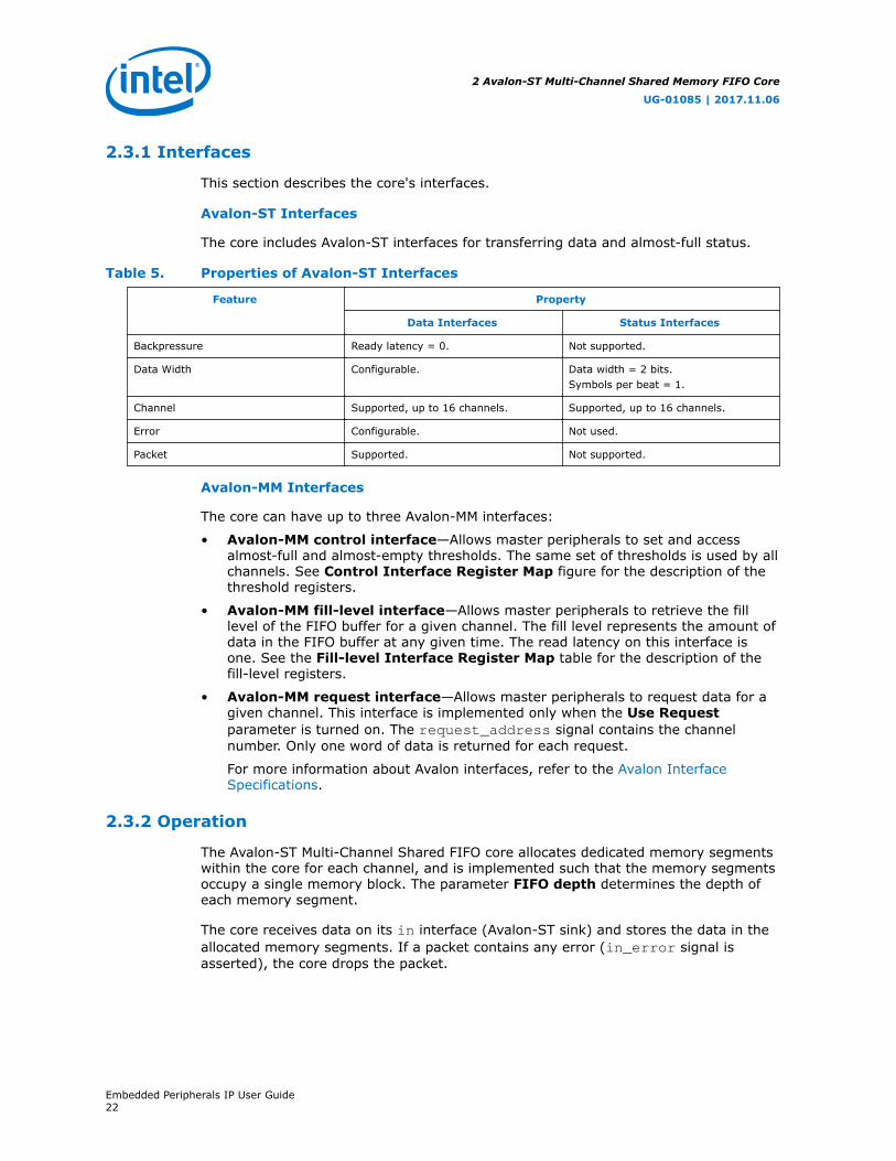
2.3.1 Interfaces
This section describes the core's interfaces.
Avalon-ST Interfaces
The core includes Avalon-ST interfaces for transferring data and almost-full status.
Table 5. Properties of Avalon-ST Interfaces
Feature Property
Data Interfaces Status Interfaces
Backpressure Ready latency = 0. Not supported.
Data Width Configurable. Data width = 2 bits.Symbols per beat = 1.
Channel Supported, up to 16 channels. Supported, up to 16 channels.
Error Configurable. Not used.
Packet Supported. Not supported.
Avalon-MM Interfaces
The core can have up to three Avalon-MM interfaces:
• Avalon-MM control interface—Allows master peripherals to set and accessalmost-full and almost-empty thresholds. The same set of thresholds is used by allchannels. See Control Interface Register Map figure for the description of thethreshold registers.
• Avalon-MM fill-level interface—Allows master peripherals to retrieve the filllevel of the FIFO buffer for a given channel. The fill level represents the amount ofdata in the FIFO buffer at any given time. The read latency on this interface isone. See the Fill-level Interface Register Map table for the description of thefill-level registers.
• Avalon-MM request interface—Allows master peripherals to request data for agiven channel. This interface is implemented only when the Use Requestparameter is turned on. The request_address signal contains the channelnumber. Only one word of data is returned for each request.
For more information about Avalon interfaces, refer to the Avalon InterfaceSpecifications.
2.3.2 Operation
The Avalon-ST Multi-Channel Shared FIFO core allocates dedicated memory segmentswithin the core for each channel, and is implemented such that the memory segmentsoccupy a single memory block. The parameter FIFO depth determines the depth ofeach memory segment.
The core receives data on its in interface (Avalon-ST sink) and stores the data in theallocated memory segments. If a packet contains any error (in_error signal isasserted), the core drops the packet.
2 Avalon-ST Multi-Channel Shared Memory FIFO Core
UG-01085 | 2017.11.06
Embedded Peripherals IP User Guide22
When the core receives a request on its request interface (Avalon-MM slave), itforwards the requested data to its out interface (Avalon-ST source) only when it hasreceived a full packet on its in interface. If the core has not received a full packet orhas no data for the requested channel, it deasserts the valid signal on its outinterface to indicate that data is not available for the channel. The output latency isthree and only one word of data can be requested at a time.
When the Avalon-MM request interface is not in use, the request_write signal iskept asserted and the request_address signal is set to 0. Hence, if you configurethe core to support more than one channel, you must also ensure that the Userequest parameter is turned on. Otherwise, only channel 0 is accessible.
You can configure almost-full thresholds to manage FIFO overflow. The currentthreshold status for each channel is available from the core's Avalon-ST statusinterfaces in a round-robin fashion. For example, if the threshold status for channel 0is available on the interface in clock cycle n, the threshold status for channel 1 isavailable in clock cycle n+1 and so forth.
2.4 Parameters
Table 6. Configurable Parameters
Parameter Legal Values Description
Number of channels 1, 2, 4, 8, and 16 The total number of channels supported on the Avalon-ST data interfaces.
Symbols per beat 1–32 The number of symbols transferred in a beat on the Avalon-ST datainterfaces
Bits per symbol 1–32 The symbol width in bits on the Avalon-ST data interfaces.
Error width 0–32 The width of the error signal on the Avalon-ST data interfaces.
FIFO depth 2–232 The depth of each memory segment allocated for a channel. The valuemust be a multiple of 2.
Use packets 0 or 1 Setting this parameter to 1 enables packet support on the Avalon-ST datainterfaces.
Use fill level 0 or 1 Setting this parameter to 1 enables the Avalon-MM status interface.
Number of almost-fullthresholds
0 to 2 The number of almost-full thresholds to enable. Setting this parameter to 1enables Use almost-full threshold 1. Setting it to 2 enables both Usealmost-full threshold 1 and Use almost-full threshold 2.
Number of almost-emptythresholds
0 to 2 The number of almost-empty thresholds to enable. Setting this parameterto 1 enables Use almost-empty threshold 1. Setting it to 2 enables bothUse almost-empty threshold 1 and Use almost-empty threshold 2.
Section available threshold 0 to 2 Address Width Specify the amount of data to be delivered to the output interface. Thisparameter applies only when packet support is disabled.
Packet buffer mode 0 or 1 Setting this parameter to 1 causes the core to deliver only full packets tothe output interface. This parameter applies only when Use packets is setto 1.
Drop on error 0 or 1 Setting this parameter to 1 causes the core to drop packets at the Avalon-ST data sink interface if the error signal on that interface is asserted.Otherwise, the core accepts the packet and sends it out on the Avalon-STdata source interface with the same error. This parameter applies onlywhen packet buffer mode is enabled.
Address width 1–32 The width of the FIFO address. This parameter is determined by theparameter FIFO depth; FIFO depth = 2 Address Width.
continued...
2 Avalon-ST Multi-Channel Shared Memory FIFO Core
UG-01085 | 2017.11.06
Embedded Peripherals IP User Guide23

Parameter Legal Values Description
Use request — Turn on this parameter to implement the Avalon-MM request interface. Ifthe core is configured to support more than one channel and the requestinterface is disabled, only channel 0 is accessible.
Use almost-full threshold 1 — Turn on these parameters to implement the optional Avalon-ST almost-fulland almost-empty interfaces and their corresponding registers. SeeControl Interface Register Map for the description of the thresholdregisters.
Use almost-full threshold 2 —
Use almost-empty threshold 1 —
Use almost-empty threshold 2 —
Use almost-full threshold 1 0 or 1 This threshold indicates that the FIFO is almost full. It is enabled when theparameter Number of almost-full threshold is set to 1 or 2.
Use almost-full threshold 2 0 or 1 This threshold is an initial indication that the FIFO is getting full. It isenabled when the parameter Number of almost-full threshold is set to2.
Use almost-empty threshold 1 0 or 1 This threshold indicates that the FIFO is almost empty. It is enabled whenthe parameter Number of almost-empty threshold is set to 1 or 2.
Use almost-empty threshold 2 0 or 1 This threshold is an initial indication that the FIFO is getting empty. It isenabled when the parameter Number of almost-empty threshold is setto 2.
2.5 Software Programming Model
The following sections describe the software programming model for the Avalon-STMulti-Channel Shared FIFO core.
2.5.1 HAL System Library Support
The Intel-provided driver implements a HAL device driver that integrates into the HALsystem library for Nios II systems. HAL users should access the Avalon-ST Multi-Channel Shared FIFO core via the familiar HAL API and the ANSI C standard library.
2.5.2 Register Map
You can configure the thresholds and retrieve the fill-level for each channel via theAvalon-MM control and fill-level interfaces respectively. Subsequent sections describethe registers accessible via each interface.
Control Register Interface
Table 7. Control Interface Register Map
ByteOffset
Name Access ResetValue
Description
0 ALMOST_FULL_THRESHOLD RW 0 Primary almost-full threshold. The bitAlmost_full_data[0] on the Avalon-STalmost-full status interface is set to 1 when theFIFO level is equal to or greater than thisthreshold.
4 ALMOST_EMPTY_THRESHOLD RW 0 Primary almost-empty threshold. The bitAlmost_empty_data[0] on the Avalon-STalmost-empty status interface is set to 1 when theFIFO level is equal to or less than this threshold.
continued...
2 Avalon-ST Multi-Channel Shared Memory FIFO Core
UG-01085 | 2017.11.06
Embedded Peripherals IP User Guide24
ByteOffset
Name Access ResetValue
Description
8 ALMOST_FULL2_THRESHOLD RW 0 Secondary almost-full threshold. The bitAlmost_full_data[1] on the Avalon-STalmost-full status interface is set to 1 when theFIFO level is equal to or greater than thisthreshold.
12 ALMOST_EMPTY2_THRESHOLD RW 0 Secondary almost-empty threshold. The bitAlmost_empty_data[1] on the Avalon-STalmost-empty status interface is set to 1 when theFIFO level is equal to or less than this threshold.
Base + 8 Almost_Empty_Threshold RW The value of the primary almost-empty threshold.The bit Almost_empty_data[0] on the Avalon-ST almost-empty status interface is set to 1 whenthe FIFO level is greater than or equal to thisthreshold.
Base+ 12
Almost_Empty2_Threshold RW The value of the secondary almost-emptythreshold. The bit Almost_empty_data[1]Avalon-ST almost-empty status interface is set to1 when the FIFO level is greater than or equal tothis threshold.
Fill-Level Register Interface
The table below shows the register map for the fill-level interface.
Table 8. Fill-level Interface Register Map
ByteOffset
Name Access ResetValue
Description
0 fill_level_0 RO 0 Fill level for each channel. Each register isdefined for each channel. For example, if thecore is configured to support four channel, fourfill-level registers are defined.
4 fill_level_1 RO 0
8 fill_level_2 RO 0
(n*4) fill_level_n RO 0
2.6 Document Revision History
Table 9. Avalon-ST Multi-Channel Shared Memory FIFO Core Revision History
Date Version Changes
December 2010 v10.1.0 Removed the “Device Support”, “Instantiating the Core in SOPC Builder”,and “Referenced Documents” sections.
July 2010 v10.0.0 Added the description of almost-empty thresholds and fill-level registers.Revised the Operation section.
November 2009 v9.1.0 No change from previous release.
March 2009 v9.0.0 No change from previous release.
November 2008 v8.1.0 Changed to 8-1/2 x 11 page size. No change to content.
May 2008 v8.0.0 Initial release.
2 Avalon-ST Multi-Channel Shared Memory FIFO Core
UG-01085 | 2017.11.06
Embedded Peripherals IP User Guide25

3 Avalon-ST Single-Clock and Dual-Clock FIFO Cores
3.1 Core Overview
The Avalon Streaming (Avalon-ST) Single-Clock and Avalon-ST Dual-Clock FIFO coresare FIFO buffers which operate with a common clock and independent clocks for inputand output ports respectively. The FIFO cores are configurable, Platform Designer-ready, and integrate easily into any Platform Designer-generated systems.
3.2 Functional Description
The following two figures show block diagrams of the Avalon-ST Single-Clock FIFO andAvalon-ST Dual-Clock FIFO cores.
Figure 3. Avalon-ST Single Clock FIFO Core
Avalon-STSingle-Clock
FIFO
Avalon-MMSlave
almost_full almost_empty
csr
Avalon-ST StatusSource
Avalon-ST StatusSource
outin Avalon-STDataSink
Avalon-STData
Source
Figure 4. Avalon-ST Dual Clock FIFO Core
Avalon-MMSlave
orsc_ni ut_csr
Avalon-MMSlave
outin
Clock A Clock B
Avalon-STDual-Clock
FIFO
Avalon-STDataSink
Avalon-STData
Source
UG-01085 | 2017.11.06
Intel Corporation. All rights reserved. Intel, the Intel logo, Altera, Arria, Cyclone, Enpirion, MAX, Nios, Quartusand Stratix words and logos are trademarks of Intel Corporation or its subsidiaries in the U.S. and/or othercountries. Intel warrants performance of its FPGA and semiconductor products to current specifications inaccordance with Intel's standard warranty, but reserves the right to make changes to any products and servicesat any time without notice. Intel assumes no responsibility or liability arising out of the application or use of anyinformation, product, or service described herein except as expressly agreed to in writing by Intel. Intelcustomers are advised to obtain the latest version of device specifications before relying on any publishedinformation and before placing orders for products or services.*Other names and brands may be claimed as the property of others.
ISO9001:2008Registered
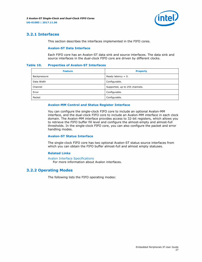
3.2.1 Interfaces
This section describes the interfaces implemented in the FIFO cores.
Avalon-ST Data Interface
Each FIFO core has an Avalon-ST data sink and source interfaces. The data sink andsource interfaces in the dual-clock FIFO core are driven by different clocks.
Table 10. Properties of Avalon-ST Interfaces
Feature Property
Backpressure Ready latency = 0.
Data Width Configurable.
Channel Supported, up to 255 channels.
Error Configurable.
Packet Configurable.
Avalon-MM Control and Status Register Interface
You can configure the single-clock FIFO core to include an optional Avalon-MMinterface, and the dual-clock FIFO core to include an Avalon-MM interface in each clockdomain. The Avalon-MM interface provides access to 32-bit registers, which allows youto retrieve the FIFO buffer fill level and configure the almost-empty and almost-fullthresholds. In the single-clock FIFO core, you can also configure the packet and errorhandling modes.
Avalon-ST Status Interface
The single-clock FIFO core has two optional Avalon-ST status source interfaces fromwhich you can obtain the FIFO buffer almost-full and almost empty statuses.
Related Links
Avalon Interface SpecificationsFor more information about Avalon interfaces.
3.2.2 Operating Modes
The following lists the FIFO operating modes:
3 Avalon-ST Single-Clock and Dual-Clock FIFO Cores
UG-01085 | 2017.11.06
Embedded Peripherals IP User Guide27

• Default mode—The core accepts incoming data on the in interface (Avalon-STdata sink) and forwards it to the out interface (Avalon-ST data source). The coreasserts the valid signal on the Avalon-ST source interface to indicate that data isavailable at the interface.
• Store and forward mode—This mode only applies to the single-clock FIFO core.The core asserts the valid signal on the out interface only when a full packet ofdata is available at the interface.
In this mode, you can also enable the drop-on-error feature by setting thedrop_on_error register to 1. When this feature is enabled, the core drops allpackets received with the in_error signal asserted.
• Cut-through mode— This mode only applies to the single-clock FIFO core. Thecore asserts the valid signal on the out interface to indicate that data isavailable for consumption when the number of entries specified in thecut_through_threshold register are available in the FIFO buffer.
To use the store and forward or cut-through mode, turn on the Use store andforward parameter to include the csr interface (Avalon-MM slave). Set thecut_through_threshold register to 0 to enable the store and forward mode;set the register to any value greater than 0 to enable the cut-through mode. Thenon-zero value specifies the minimum number of FIFO entries that must beavailable before the data is ready for consumption. Setting the register to 1provides you with the default mode.
3.2.3 Fill Level
You can obtain the fill level of the FIFO buffer via the optional Avalon-MM control andstatus interface. Turn on the Use fill level parameter (Use sink fill level and Usesource fill level in the dual-clock FIFO core) and read the fill_level register.
The dual-clock FIFO core has two fill levels, one in each clock domain. Due to thelatency of the clock crossing logic, the fill levels reported in the input and output clockdomains may be different at any given instance. In both cases, the fill level ispessimistic for the clock domain; the fill level is reported high in the input clockdomain and low in the output clock domain.
The dual-clock FIFO has an output pipeline stage to improve fMAX. This output stage isaccounted for when calculating the output fill level, but not when calculating the inputfill level. Hence, the best measure of the amount of data in the FIFO is given by the filllevel in the output clock domain, while the fill level in the input clock domainrepresents the amount of space available in the FIFO (Available space = FIFO depth– input fill level).
3.2.4 Thresholds
You can use almost-full and almost-empty thresholds as a mechanism to prevent FIFOoverflow and underflow. This feature is only available in the single-clock FIFO core.
To use the thresholds, turn on the Use fill level, Use almost-full status, and Usealmost-empty status parameters. You can access the almost_full_thresholdand almost_full_threshold registers via the csr interface and set the registers toan optimal value for your application.
3 Avalon-ST Single-Clock and Dual-Clock FIFO Cores
UG-01085 | 2017.11.06
Embedded Peripherals IP User Guide28

You can obtain the almost-full and almost-empty statuses from almost_full andalmost_empty interfaces (Avalon-ST status source). The core asserts thealmost_full signal when the fill level is equal to or higher than the almost-fullthreshold. Likewise, the core asserts the almost_empty signal when the fill level isequal to or lower than the almost-empty threshold.
3.3 Parameters
Table 11. Configurable Parameters
Parameter Legal Values Description
Bits per symbol 1–32 These parameters determine the width of the FIFO.FIFO width = Bits per symbol * Symbols per beat, where:Bits per symbol is the number of bits in a symbol, andSymbols per beat is the number of symbols transferred in a beat.
Symbols per beat 1–32
Error width 0–32 The width of the error signal.
FIFO depth 1–32 The FIFO depth. An output pipeline stage is added to the FIFO to increaseperformance, which increases the FIFO depth by one.
Use packets — Turn on this parameter to enable packet support on the Avalon-ST data interfaces.
Channel width 1–32 The width of the channel signal.
Avalon-ST Single Clock FIFO Only
Use fill level — Turn on this parameter to include the Avalon-MM control and status registerinterface.
Avalon-ST Dual Clock FIFO Only
Use sink fill level — Turn on this parameter to include the Avalon-MM control and status registerinterface in the input clock domain.
Use source fill level — Turn on this parameter to include the Avalon-MM control and status registerinterface in the output clock domain.
Write pointersynchronizer length
2–8 The length of the write pointer synchronizer chain. Setting this parameter to ahigher value leads to better metastability while increasing the latency of the core.
Read pointersynchronizer length
2–8 The length of the read pointer synchronizer chain. Setting this parameter to ahigher value leads to better metastability.
Use Max Channel — Turn on this parameter to specify the maximum channel number.
Max Channel 1–255 Maximum channel number.
For more information on metastability in Intel FPGA devices, refer to AN 42:Metastability in Intel FPGA devices.
For more information on metastability analysis and synchronization register chains,refer to the Area and Timing Optimization chapter in volume 2 of the Intel QuartusPrime Handbook.
3.4 Register Description
The csr interface in the Avalon-ST Single Clock FIFO core provides access toregisters. The table below describes the registers.
3 Avalon-ST Single-Clock and Dual-Clock FIFO Cores
UG-01085 | 2017.11.06
Embedded Peripherals IP User Guide29

Table 12. Register Description for Avalon-ST Single-Clock FIFO
32-Bit WordOffset
Name Access Reset Description
0 fill_level R 0 24-bit FIFO fill level. Bits 24 to 31 areunused.
1 Reserved — — Reserved for future use.
2 almost_full_threshold RW FIFO depth–1 Set this register to a value that indicatesthe FIFO buffer is getting full.
3 almost_empty_threshold RW 0 Set this register to a value that indicatesthe FIFO buffer is getting empty.
4 cut_through_threshold RW 0 0—Enables store and forward mode.>0—Enables cut-through mode andspecifies the minimum of entries in theFIFO buffer before the valid signal onthe Avalon-ST source interface isasserted. Once the FIFO core startssending the data to the downstreamcomponent, it continues to do so untilthe end of the packet.This register applies only when the Usestore and forward parameter is turnedon.
5 drop_on_error RW 0 0—Disables drop-on error.1—Enables drop-on error.This register applies only when the Usepacket and Use store and forwardparameters are turned on.
The in_csr and out_csr interfaces in the Avalon-ST Dual Clock FIFO core reportsthe FIFO fill level. The table below describes the fill level.
Table 13. Register Description for Avalon-ST Dual-Clock FIFO
32-Bit WordOffset
Name Access ResetValue
Description
0 fill_level R 0 24-bit FIFO fill level. Bits 24 to 31 are unused.
1 threshold RW Almost-full threshold in the input port domain;almost-empty threshold in the output portdomain.
3.5 Document Revision History
Table 14. Avalon-ST Single-Clock and Dual-Clock FIFO Core Revision History
Date Version Changes
December 2010 v10.1.0 Removed the “Device Support”, “Instantiating the Core in SOPC Builder”,and “Referenced Documents” sections.
July 2010 v10.0.0 Added description of the new features of the single-clock FIFO: store andforward mode, cut-through mode, and drop on error.Added parameters and registers.
November 2009 v9.1.0 No change from previous release.
continued...
3 Avalon-ST Single-Clock and Dual-Clock FIFO Cores
UG-01085 | 2017.11.06
Embedded Peripherals IP User Guide30

Date Version Changes
March 2009 v9.0.0 Added description of new parameters, Write pointer synchronizerlength and Read pointer synchronizer length.
November 2008 v8.1.0 Changed to 8-1/2 x 11 page size. No change to content.
May 2008 v8.0.0 Initial release.
3 Avalon-ST Single-Clock and Dual-Clock FIFO Cores
UG-01085 | 2017.11.06
Embedded Peripherals IP User Guide31
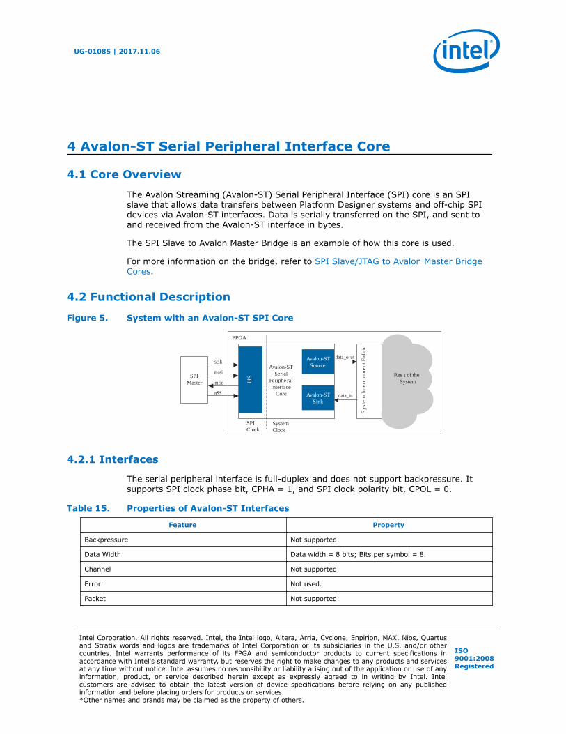
4 Avalon-ST Serial Peripheral Interface Core
4.1 Core Overview
The Avalon Streaming (Avalon-ST) Serial Peripheral Interface (SPI) core is an SPIslave that allows data transfers between Platform Designer systems and off-chip SPIdevices via Avalon-ST interfaces. Data is serially transferred on the SPI, and sent toand received from the Avalon-ST interface in bytes.
The SPI Slave to Avalon Master Bridge is an example of how this core is used.
For more information on the bridge, refer to SPI Slave/JTAG to Avalon Master BridgeCores.
4.2 Functional Description
Figure 5. System with an Avalon-ST SPI Core
Avalon-STSource
Avalon-STSink
Avalon-STSerial
Periphe ralInterface
Core
SPI
aF tcennocretnI
metsyS
bcir
Res t of the System
data_o ut
data_in
SPI Master
mosi
miso
sclk
nSS
FPGA
SPIClock
SystemClock
4.2.1 Interfaces
The serial peripheral interface is full-duplex and does not support backpressure. Itsupports SPI clock phase bit, CPHA = 1, and SPI clock polarity bit, CPOL = 0.
Table 15. Properties of Avalon-ST Interfaces
Feature Property
Backpressure Not supported.
Data Width Data width = 8 bits; Bits per symbol = 8.
Channel Not supported.
Error Not used.
Packet Not supported.
UG-01085 | 2017.11.06
Intel Corporation. All rights reserved. Intel, the Intel logo, Altera, Arria, Cyclone, Enpirion, MAX, Nios, Quartusand Stratix words and logos are trademarks of Intel Corporation or its subsidiaries in the U.S. and/or othercountries. Intel warrants performance of its FPGA and semiconductor products to current specifications inaccordance with Intel's standard warranty, but reserves the right to make changes to any products and servicesat any time without notice. Intel assumes no responsibility or liability arising out of the application or use of anyinformation, product, or service described herein except as expressly agreed to in writing by Intel. Intelcustomers are advised to obtain the latest version of device specifications before relying on any publishedinformation and before placing orders for products or services.*Other names and brands may be claimed as the property of others.
ISO9001:2008Registered
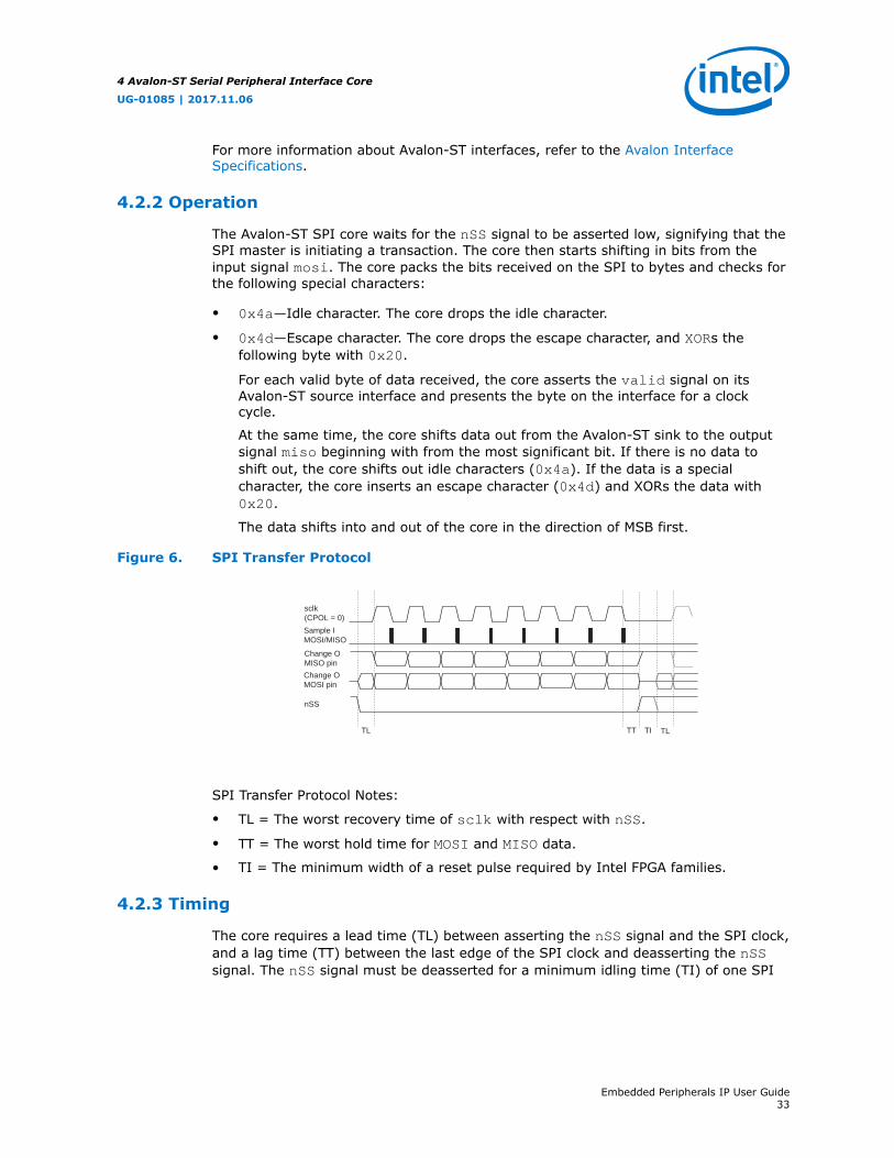
For more information about Avalon-ST interfaces, refer to the Avalon InterfaceSpecifications.
4.2.2 Operation
The Avalon-ST SPI core waits for the nSS signal to be asserted low, signifying that theSPI master is initiating a transaction. The core then starts shifting in bits from theinput signal mosi. The core packs the bits received on the SPI to bytes and checks forthe following special characters:
• 0x4a—Idle character. The core drops the idle character.
• 0x4d—Escape character. The core drops the escape character, and XORs thefollowing byte with 0x20.
For each valid byte of data received, the core asserts the valid signal on itsAvalon-ST source interface and presents the byte on the interface for a clockcycle.
At the same time, the core shifts data out from the Avalon-ST sink to the outputsignal miso beginning with from the most significant bit. If there is no data toshift out, the core shifts out idle characters (0x4a). If the data is a specialcharacter, the core inserts an escape character (0x4d) and XORs the data with0x20.
The data shifts into and out of the core in the direction of MSB first.
Figure 6. SPI Transfer Protocol
sclk (CPOL = 0)
Sample IMOSI/MISO
Change OMISO pin
Change OMOSI pin
nSS
TL TT TI TL
SPI Transfer Protocol Notes:
• TL = The worst recovery time of sclk with respect with nSS.
• TT = The worst hold time for MOSI and MISO data.
• TI = The minimum width of a reset pulse required by Intel FPGA families.
4.2.3 Timing
The core requires a lead time (TL) between asserting the nSS signal and the SPI clock,and a lag time (TT) between the last edge of the SPI clock and deasserting the nSSsignal. The nSS signal must be deasserted for a minimum idling time (TI) of one SPI
4 Avalon-ST Serial Peripheral Interface Core
UG-01085 | 2017.11.06
Embedded Peripherals IP User Guide33

clock between byte transfers. A Timing Analyzer SDC file (.sdc) is provided to removefalse timing paths. The frequency of the SPI master’s clock must be equal to or lowerthan the frequency of the core’s clock.
4.2.4 Limitations
Daisy-chain configuration, where the output line miso of an instance of the core isconnected to the input line mosi of another instance, is not supported.
4.3 Configuration
The parameter Number of synchronizer stages: Depth allows you to specify thelength of synchronization register chains. These register chains are used when ametastable event is likely to occur and the length specified determines the meantimebefore failure. The register chain length, however, affects the latency of the core.
For more information on metastability in Intel FPGA devices, refer to AN 42:Metastability in Intel FPGA devices.
For more information on metastability analysis and synchronization register chains,refer to the Area and Timing Optimization chapter in volume 2 of the Intel QuartusPrime Handbook.
4.4 Document Revision History
Table 16. Avalon-ST Serial Peripheral Interface Core Revision History
Date Version Changes
July 2014 2014.07.24 Removed mention of SOPC Builder, updated to Platform Designer
December 2010 v10.1.0 Removed the “Device Support”, “Instantiating the Core in SOPC Builder”,and “Referenced Documents” sections.
July 2010 v10.0.0 No change from previous release.
November 2009 v9.1.0 Added a description to specify the shift direction.
March 2009 v9.0.0 Added description of a new parameter, Number of synchronizer stages:Depth.
November 2008 v8.1.0 Changed to 8-1/2 x 11 page size. No change to content.
May 2008 v8.0.0 Initial release.
4 Avalon-ST Serial Peripheral Interface Core
UG-01085 | 2017.11.06
Embedded Peripherals IP User Guide34

5 SPI Core
5.1 Core Overview
SPI is an industry-standard serial protocol commonly used in embedded systems toconnect microprocessors to a variety of off-chip sensor, conversion, memory, andcontrol devices. The SPI core with Avalon interface implements the SPI protocol andprovides an Avalon Memory-Mapped (Avalon-MM) interface on the back end.
The SPI core can implement either the master or slave protocol. When configured as amaster, the core can control up to 32 independent SPI slaves. The width of the receiveand transmit registers are configurable between 1 and 32 bits. Longer transfer lengthscan be supported with software routines. The core provides an interrupt output thatcan flag an interrupt whenever a transfer completes.
5.2 Functional Description
The SPI core communicates using two data lines, a control line, and a synchronizationclock:
• Master Out Slave In (mosi)—Output data from the master to the inputs of theslaves
• Master In Slave Out (miso)—Output data from a slave to the input of the master
• Serial Clock (sclk)—Clock driven by the master to slaves, used to synchronizethe data bits
• Slave Select (ss_n)— Select signal (active low) driven by the master to individualslaves, used to select the target slave
The SPI core has the following user-visible features:
• A memory-mapped register space comprised of five registers: rxdata, txdata,status, control, and slaveselect
• Four SPI interface ports: sclk, ss_n, mosi, and miso
The registers provide an interface to the SPI core and are visible via the Avalon-MM slave port. The sclk, ss_n, mosi, and miso ports provide the hardwareinterface to other SPI devices. The behavior of sclk, ss_n, mosi, and misodepends on whether the SPI core is configured as a master or slave.
UG-01085 | 2017.11.06
Intel Corporation. All rights reserved. Intel, the Intel logo, Altera, Arria, Cyclone, Enpirion, MAX, Nios, Quartusand Stratix words and logos are trademarks of Intel Corporation or its subsidiaries in the U.S. and/or othercountries. Intel warrants performance of its FPGA and semiconductor products to current specifications inaccordance with Intel's standard warranty, but reserves the right to make changes to any products and servicesat any time without notice. Intel assumes no responsibility or liability arising out of the application or use of anyinformation, product, or service described herein except as expressly agreed to in writing by Intel. Intelcustomers are advised to obtain the latest version of device specifications before relying on any publishedinformation and before placing orders for products or services.*Other names and brands may be claimed as the property of others.
ISO9001:2008Registered
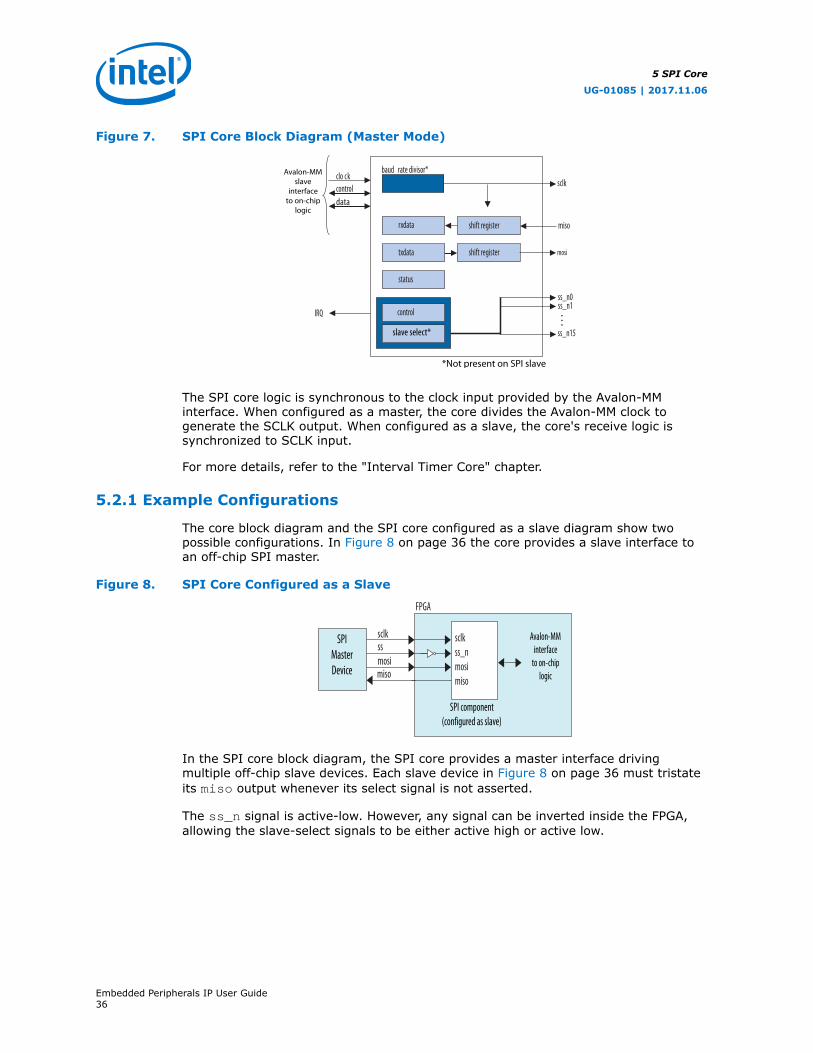
Figure 7. SPI Core Block Diagram (Master Mode)
clo ckcontrol
control
baud rate divisor*
IRQ
sclk
mosi
miso
ss_n0ss_n1
ss_n15
*Not present on SPI slave
txdata shift register
status
rxdata shift register
data
Avalon-MMslave
interfaceto on-chip
logic
slave select*
The SPI core logic is synchronous to the clock input provided by the Avalon-MMinterface. When configured as a master, the core divides the Avalon-MM clock togenerate the SCLK output. When configured as a slave, the core's receive logic issynchronized to SCLK input.
For more details, refer to the "Interval Timer Core" chapter.
5.2.1 Example Configurations
The core block diagram and the SPI core configured as a slave diagram show twopossible configurations. In Figure 8 on page 36 the core provides a slave interface toan off-chip SPI master.
Figure 8. SPI Core Configured as a Slave
FPGA
sclkss_nmosimiso
misomosisssclkSPI
MasterDevice
SPI component(configured as slave)
Avalon-MMinterface
to on-chiplogic
In the SPI core block diagram, the SPI core provides a master interface drivingmultiple off-chip slave devices. Each slave device in Figure 8 on page 36 must tristateits miso output whenever its select signal is not asserted.
The ss_n signal is active-low. However, any signal can be inverted inside the FPGA,allowing the slave-select signals to be either active high or active low.
5 SPI Core
UG-01085 | 2017.11.06
Embedded Peripherals IP User Guide36

5.2.2 Transmitter Logic
The core transmitter logic consists of a transmit holding register (txdata) andtransmit shift register, each n bits wide. The register width n is specified at systemgeneration time, and can be any integer value from 8 to 32. After a master peripheralwrites a value to the txdata register, the value is copied to the shift register and thentransmitted when the next operation starts.
The shift register and the txdata register provide double buffering during datatransmission. A new value can be written into the txdata register while the previousdata is being shifted out of the shift register. The transmitter logic automaticallytransfers the txdata register to the shift register whenever a serial shift operation isnot currently in process.
In master mode, the transmit shift register directly feeds the mosi output. In slavemode, the transmit shift register directly feeds the miso output. Data shifts out LSBfirst or MSB first, depending on the configuration of the SPI core.
5.2.3 Receiver Logic
The core receive logic consists of a receive holding register (rxdata) and receive shiftregister, each n bits wide. The register width n is specified at system generation time,and can be any integer value from 8 to 32. A master peripheral reads received datafrom the rxdata register after the shift register has captured a full n-bit value ofdata.
The shift register and the rxdata register provide double buffering while receivingdata. The rxdata register can hold a previously received data value while subsequentnew data is shifting into the shift register. The receiver logic automatically transfersthe shift register content to the rxdata register when a serial shift operationcompletes.
In master mode, the shift register is fed directly by the miso input. In slave mode,the shift register is fed directly by the mosi input. The receiver logic expects inputdata to arrive LSB first or MSB first, depending on the configuration of the SPI core.
5.2.4 Master and Slave Modes
At system generation time, the designer configures the SPI core in either mastermode or slave mode. The mode cannot be switched at runtime.
5.2.4.1 Master Mode Operation
In master mode, the SPI ports behave as shown in the table below.
Table 17. Master Mode Port Configurations
Name Direction Description
mosi output Data output to slave(s)
miso input Data input from slave(s)
sclk output Synchronization clock to all slaves
ss_nM output Slave select signal to slave M, where M is a number between 0 and 31.
5 SPI Core
UG-01085 | 2017.11.06
Embedded Peripherals IP User Guide37
In master mode, an intelligent host (for example, a microprocessor) configures theSPI core using the control and slaveselect registers, and then writes data to thetxdata buffer to initiate a transaction. A master peripheral can monitor the status ofthe transaction by reading the status register. A master peripheral can enableinterrupts to notify the host whenever new data is received (for example, a transferhas completed), or whenever the transmit buffer is ready for new data.
The SPI protocol is full duplex, so every transaction both sends and receives data atthe same time. The master transmits a new data bit on the mosi output and the slavedrives a new data bit on the miso input for each active edge of sclk. The SPI coredivides the Avalon-MM system clock using a clock divider to generate the sclk signal.
When the SPI core is configured to interface with multiple slaves, the core has oness_n signal for each slave. During a transfer, the master asserts ss_n to each slavespecified in the slaveselect register. Note that there can be no more than one slavetransmitting data during any particular transfer, or else there will be a contention onthe miso input. The number of slave devices is specified at system generation time.
5.2.4.2 Slave Mode Operation
In slave mode, the SPI ports behave as shown in the table below.
Table 18. Slave Mode Port Configurations
Name Direction Description
mosi input Data input from the master
miso output Data output to the master
sclk input Synchronization clock
ss_n input Select signal
In slave mode, the SPI core simply waits for the master to initiate transactions. Beforea transaction begins, the slave logic continuously polls the ss_n input. When themaster asserts ss_n, the slave logic immediately begins sending the transmit shiftregister contents to the miso output. The slave logic also captures data on the mosiinput, and fills the receive shift register simultaneously. After a word is received by theslave, the master must de-assert the ss_n signal and reasserts the signal again whenthe next word is ready to be sent.
An intelligent host such as a microprocessor writes data to the txdata registers, sothat it is transmitted the next time the master initiates an operation. A masterperipheral reads received data from the rxdata register. A master peripheral canenable interrupts to notify the host whenever new data is received, or whenever thetransmit buffer is ready for new data.
5.2.4.3 Multi-Slave Environments
When ss_n is not asserted, typical SPI cores set their miso output pins to highimpedance. The provided SPI slave core drives an undefined high or low value on itsmiso output when not selected. Special consideration is necessary to avoid signalcontention on the miso output, if the SPI core in slave mode is connected to an off-chip SPI master device with multiple slaves. In this case, the ss_n input should beused to control a tristate buffer on the miso signal.
5 SPI Core
UG-01085 | 2017.11.06
Embedded Peripherals IP User Guide38

Figure 9. SPI Core in a Multi-Slave Environment
SPIMasterDevice
sclk mosi misoss_n0ss_01
sclk mosi miso
ss_n0
SPI SlaveDeviceSS_n
misomosisclk
SPI component(configured as slave)
5.3 Configuration
The following sections describe the available configuration options.
5.3.1 Master/Slave Settings
The designer can select either master mode or slave mode to determine the role ofthe SPI core. When master mode is selected, the following options are available:Number of select (SS_n) signals, SPI clock rate, and Specify delay.
5.3.1.1 Number of Select (SS_n) Signals
This setting specifies the number of slaves the SPI master connects to. The range is 1to 32. The SPI master core presents a unique ss_n signal for each slave.
5.3.1.2 SPI Clock (sclk) Rate
This setting determines the rate of the sclk signal that synchronizes data betweenmaster and slaves. The target clock rate can be specified in units of Hz, kHz or MHz.The SPI master core uses the Avalon-MM system clock and a clock divisor to generatesclk.
The actual frequency of sclk may not exactly match the desired target clock rate.The achievable clock values are:
<Avalon-MM system clock frequency> / [2, 4, 6, 8, ...]
The actual frequency achieved will not be greater than the specified target value.
5 SPI Core
UG-01085 | 2017.11.06
Embedded Peripherals IP User Guide39
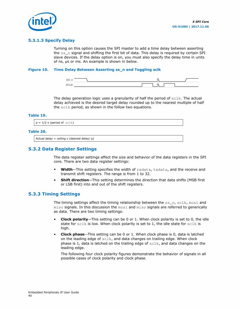
5.3.1.3 Specify Delay
Turning on this option causes the SPI master to add a time delay between assertingthe ss_n signal and shifting the first bit of data. This delay is required by certain SPIslave devices. If the delay option is on, you must also specify the delay time in unitsof ns, µs or ms. An example is shown in below.
Figure 10. Time Delay Between Asserting ss_n and Toggling sclk
The delay generation logic uses a granularity of half the period of sclk. The actualdelay achieved is the desired target delay rounded up to the nearest multiple of halfthe sclk period, as shown in the follow two equations.
Table 19.
p = 1/2 x (period of sclk)
Table 20.
Actual delay = ceiling x (desired delay/ p)
5.3.2 Data Register Settings
The data register settings affect the size and behavior of the data registers in the SPIcore. There are two data register settings:
• Width—This setting specifies the width of rxdata, txdata, and the receive andtransmit shift registers. The range is from 1 to 32.
• Shift direction—This setting determines the direction that data shifts (MSB firstor LSB first) into and out of the shift registers.
5.3.3 Timing Settings
The timing settings affect the timing relationship between the ss_n, sclk, mosi andmiso signals. In this discussion the mosi and miso signals are referred to genericallyas data. There are two timing settings:
• Clock polarity—This setting can be 0 or 1. When clock polarity is set to 0, the idlestate for sclk is low. When clock polarity is set to 1, the idle state for sclk ishigh.
• Clock phase—This setting can be 0 or 1. When clock phase is 0, data is latchedon the leading edge of sclk, and data changes on trailing edge. When clockphase is 1, data is latched on the trailing edge of sclk, and data changes on theleading edge.
The following four clock polarity figures demonstrate the behavior of signals in allpossible cases of clock polarity and clock phase.
5 SPI Core
UG-01085 | 2017.11.06
Embedded Peripherals IP User Guide40

Figure 11. Clock Polarity = 0, Clock Phase = 0
Figure 12. Clock Polarity = 0, Clock Phase = 1
Figure 13. Clock Polarity = 1, Clock Phase = 0
Figure 14. Clock Polarity = 1, Clock Phase = 1
5.4 Software Programming Model
The following sections describe the software programming model for the SPI core,including the register map and software constructs used to access the hardware. ForNios II processor users, Intel provides the HAL system library header file that definesthe SPI core registers. The SPI core does not match the generic device modelcategories supported by the HAL, so it cannot be accessed via the HAL API or theANSI C standard library. Intel provides a routine to access the SPI hardware that isspecific to the SPI core.
5.4.1 Hardware Access Routines
Intel provides one access routine, alt_avalon_spi_command(), that providesgeneral-purpose access to the SPI core that is configured as a master.
5.4.1.1 alt_avalon_spi_command()
Prototype: int alt_avalon_spi_command(alt_u32 base, alt_u32 slave,
alt_u32 write_length, const alt_u8* wdata,
alt_u32 read_length,
alt_u8* read_data,
continued...
5 SPI Core
UG-01085 | 2017.11.06
Embedded Peripherals IP User Guide41

alt_u32 flags)
Thread-safe: No.
Available from ISR: No.
Include: <altera_avalon_spi.h>
Description: This function performs a control sequence on the SPI bus. It supports only SPI masters with datawidth less than or equal to 8 bits. A single call to this function writes a data buffer of arbitrarylength to the mosi port, and then reads back an arbitrary amount of data from the miso port. Thefunction performs the following actions:(1) Asserts the slave select output for the specified slave. The first slave select output is 0.(2) Transmits write_length bytes of data from wdata through the SPI interface, discarding theincoming data on the miso port.(3) Reads read_length bytes of data and stores the data into the buffer pointed to by read_data.The mosi port is set to zero during the read transaction.(4) De-asserts the slave select output, unless the flags field contains the valueALT_AVALON_SPI_COMMAND_MERGE. If you want to transmit from scattered buffers, call thefunction multiple times and specify the merge flag on all the accesses except the last.To access the SPI bus from more than one thread, you must use a semaphore or mutex to ensurethat only one thread is executing within this function at any time.
Returns: The number of bytes stored in the read_data buffer.
5.4.2 Software Files
The core is accompanied by the following software files. These files provide a low-levelinterface to the hardware.
• altera_avalon_spi.h—This file defines the core's register map, providingsymbolic constants to access the low-level hardware.
• altera_avalon_spi.c—This file implements low-level routines to access thehardware.
5 SPI Core
UG-01085 | 2017.11.06
Embedded Peripherals IP User Guide42
5.4.3 Register Map
An Avalon-MM master peripheral controls and communicates with the core via the six32-bit registers, shown in below in the Register Map for SPI Master Device figure.The table assumes an n-bit data width for rxdata and txdata.
Table 21. Register Map for SPI Master Device
InternalAddress
Register Name Type[R/W]
32-11
10 9 8 7 6 5 4 3 2-0
0 rxdata (3) R RXDATA (n-1..0)
1 txdata (3) W TXDATA (n-1..0)
2 status (1) R/W EOP E RRDY TRDY TMT TOE ROE
3 control R/W SSO(2)
IEOP IE IRRDY
ITRDY
ITOE IROE
4 Reserved —
5 slaveselect (2) R/W Slave Select Mask
6 eop_value(3) R/W End of Packet Value (n-1..0)
Reading undefined bits returns an undefined value. Writing to undefined bits has noeffect.
5.4.3.1 rxdata Register
A master peripheral reads received data from the rxdata register. When the receiveshift register receives a full n bits of data, the status register's RRDY bit is set to 1and the data is transferred into the rxdata register. Reading the rxdata registerclears the RRDY bit. Writing to the rxdata register has no effect.
New data is always transferred into the rxdata register, whether or not the previousdata was retrieved. If RRDY is 1 when data is transferred into the rxdata register(that is, the previous data was not retrieved), a receive-overrun error occurs and thestatus register's ROE bit is set to 1. In this case, the contents of rxdata areundefined.
5.4.3.2 txdata Register
A master peripheral writes data to be transmitted into the txdata register. When thestatus register's TRDY bit is 1, it indicates that the txdata register is ready for newdata. The TRDY bit is set to 0 whenever the txdata register is written. The TRDY bitis set to 1 after data is transferred from the txdata register into the transmitter shiftregister, which readies the txdata holding register to receive new data.
(1) A write operation to the status register clears the ROE, TOE, and E bits.
(2) Present only in master mode.
(3) Bits 31 to n are undefined when n is less than 32.
5 SPI Core
UG-01085 | 2017.11.06
Embedded Peripherals IP User Guide43

A master peripheral should not write to the txdata register until the transmitter isready for new data. If TRDY is 0 and a master peripheral writes new data to thetxdata register, a transmit-overrun error occurs and the status register's TOE bit isset to 1. In this case, the new data is ignored, and the content of txdata remainsunchanged.
As an example, assume that the SPI core is idle (that is, the txdata register andtransmit shift register are empty), when a CPU writes a data value into the txdataholding register. The TRDY bit is set to 0 momentarily, but after the data in txdata istransferred into the transmitter shift register, TRDY returns to 1. The CPU writes asecond data value into the txdata register, and again the TRDY bit is set to 0. Thistime the shift register is still busy transferring the original data value, so the TRDY bitremains at 0 until the shift operation completes. When the operation completes, thesecond data value is transferred into the transmitter shift register and the TRDY bit isagain set to 1.
5.4.3.3 status Register
The status register consists of bits that indicate status conditions in the SPI core.Each bit is associated with a corresponding interrupt-enable bit in the controlregister, as discussed in the Control Register section. A master peripheral can readstatus at any time without changing the value of any bits. Writing status does clearthe ROE, TOE and E bits.
Table 22. status Register Bits
# Name Description
3 ROE Receive-overrun errorThe ROE bit is set to 1 if new data is received while the rxdata register is full (that is, while the RRDYbit is 1). In this case, the new data overwrites the old. Writing to the status register clears the ROE bitto 0.
4 TOE Transmitter-overrun errorThe TOE bit is set to 1 if new data is written to the txdata register while it is still full (that is, while theTRDY bit is 0). In this case, the new data is ignored. Writing to the status register clears the TOE bitto 0.
5 TMT Transmitter shift-register emptyIn master mode, the TMT bit is set to 0 when a transaction is in progress and set to 1 when the shiftregister is empty.In slave mode, the TMT bit is set to 0 when the slave is selected (SS_n is low) or when the SPI Slaveregister interface is not ready to receive data.
6 TRDY Transmitter readyThe TRDY bit is set to 1 when the txdata register is empty.
7 RRDY Receiver readyThe RRDY bit is set to 1 when the rxdata register is full.
8 E ErrorThe E bit is the logical OR of the TOE and ROE bits. This is a convenience for the programmer to detecterror conditions. Writing to the status register clears the E bit to 0.
9 EOP End of PacketThe EOP bit is set when the End of Packet condition is detected. The End of Packet condition is detectedwhen either the read data of the rxdata register or the write data to the txdata register is matchingthe content of the eop_value register.
5 SPI Core
UG-01085 | 2017.11.06
Embedded Peripherals IP User Guide44
5.4.3.4 control Register
The control register consists of data bits to control the SPI core's operation. Amaster peripheral can read control at any time without changing the value of anybits.
Most bits (IROE, ITOE, ITRDY, IRRDY, and IE) in the control register controlinterrupts for status conditions represented in the status register. For example, bit 1of status is ROE (receiver-overrun error), and bit 1 of control is IROE, which enablesinterrupts for the ROE condition. The SPI core asserts an interrupt request when thecorresponding bits in status and control are both 1.
Table 23. control Register Bits
# Name Description
3 IROE Setting IROE to 1 enables interrupts for receive-overrun errors.
4 ITOE Setting ITOE to 1 enables interrupts for transmitter-overrun errors.
6 ITRDY Setting ITRDY to 1 enables interrupts for the transmitter ready condition.
7 IRRDY Setting IRRDY to 1 enables interrupts for the receiver ready condition.
8 IE Setting IE to 1 enables interrupts for any error condition.
9 IEOP Setting IEOP to 1 enables interrupts for the End of Packet condition.
10 SSO Setting SSO to 1 forces the SPI core to drive its ss_n outputs, regardless of whether a serial shiftoperation is in progress or not. The slaveselect register controls which ss_n outputs are asserted.SSO can be used to transmit or receive data of arbitrary size, for example, greater than 32 bits.
After reset, all bits of the control register are set to 0. All interrupts are disabledand no ss_n signals are asserted.
5.4.3.5 slaveselect Register
The slaveselect register is a bit mask for the ss_n signals driven by an SPI master.During a serial shift operation, the SPI master selects only the slave device(s)specified in the slaveselect register.
The slaveselect register is only present when the SPI core is configured in mastermode. There is one bit in slaveselect for each ss_n output, as specified by thedesigner at system generation time.
A master peripheral can set multiple bits of slaveselect simultaneously, causing theSPI master to simultaneously select multiple slave devices as it performs atransaction. For example, to enable communication with slave devices 1, 5, and 6, setbits 1, 5, and 6 of slaveselect. However, consideration is necessary to avoid signalcontention between multiple slaves on their miso outputs.
Upon reset, bit 0 is set to 1, and all other bits are cleared to 0. Thus, after a devicereset, slave device 0 is automatically selected.
5.4.3.6 end of packet value Register
The end of packet value register allows you to specify the value of the SPI data word.The SPI data word acts as the end of packet word.
5 SPI Core
UG-01085 | 2017.11.06
Embedded Peripherals IP User Guide45
5.5 Document Revision History
Table 24. SPI Core Document Revision History
Date Version Changes
June 2016 2016.06.17 Updates:• Removed content regarding Avalon-MM flow control• Table 21 on page 43: eop_value added• Table 22 on page 44: EOP added• Table 23 on page 45: IEOP added• end of packet value Register on page 45: New topic
December 2010 v10.1.0 Removed the “Device Support”, “Instantiating the Core in SOPC Builder”,and “Referenced Documents” sections.
July 2010 v10.0.0 No change from previous release.
November 2009 v9.1.0 Revised register width in transmitter logic and receiver logic.Added description on the disable flow control option.Added R/W column in Table 8–3 .
March 2009 v9.0.0 No change from previous release.
November 2008 v8.1.0 Changed to 8-1/2 x 11 page size. Updated the width of the parametersand signals from 16 to 32.
May 2008 v8.0.0 Updated the description of the TMT bit.
5 SPI Core
UG-01085 | 2017.11.06
Embedded Peripherals IP User Guide46
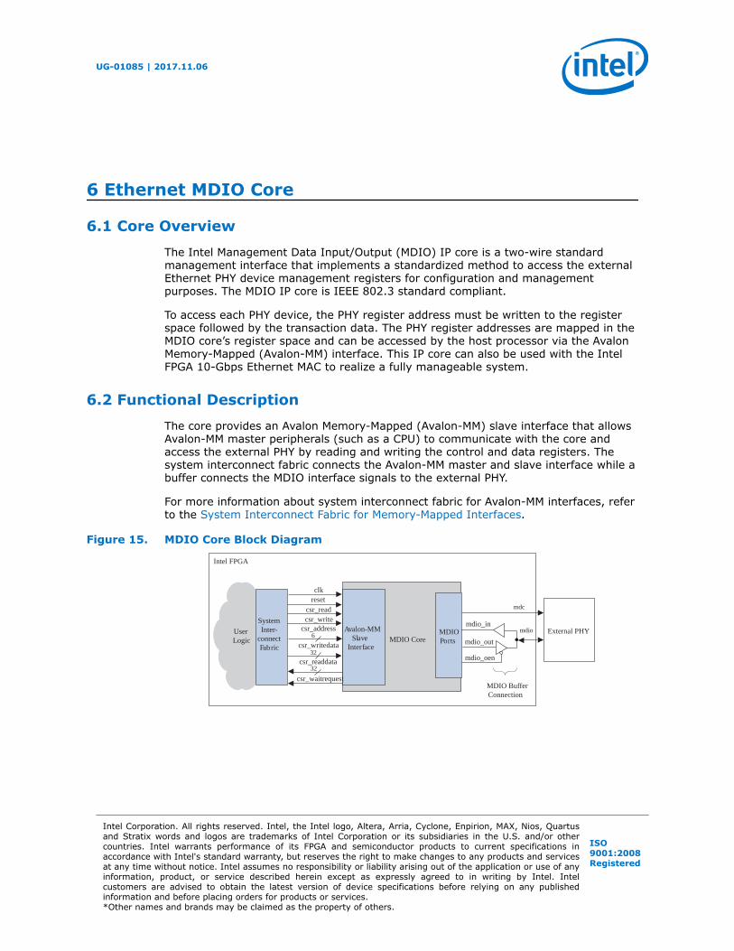
6 Ethernet MDIO Core
6.1 Core Overview
The Intel Management Data Input/Output (MDIO) IP core is a two-wire standardmanagement interface that implements a standardized method to access the externalEthernet PHY device management registers for configuration and managementpurposes. The MDIO IP core is IEEE 802.3 standard compliant.
To access each PHY device, the PHY register address must be written to the registerspace followed by the transaction data. The PHY register addresses are mapped in theMDIO core’s register space and can be accessed by the host processor via the AvalonMemory-Mapped (Avalon-MM) interface. This IP core can also be used with the IntelFPGA 10-Gbps Ethernet MAC to realize a fully manageable system.
6.2 Functional Description
The core provides an Avalon Memory-Mapped (Avalon-MM) slave interface that allowsAvalon-MM master peripherals (such as a CPU) to communicate with the core andaccess the external PHY by reading and writing the control and data registers. Thesystem interconnect fabric connects the Avalon-MM master and slave interface while abuffer connects the MDIO interface signals to the external PHY.
For more information about system interconnect fabric for Avalon-MM interfaces, referto the System Interconnect Fabric for Memory-Mapped Interfaces.
Figure 15. MDIO Core Block Diagram
csr_addressmdio_in
MDIO Core mdio_out
clk
Avalon-MMSlave
Interface
csr_waitrequest
MDIOPorts
External PHY
mdc
mdio
csr_readcsr_write
csr_writedata
csr_readdata
reset
mdio_oen
MDIO BufferConnection
32
32
6
SystemInter-
connectFabric
UserLogic
Intel FPGA
UG-01085 | 2017.11.06
Intel Corporation. All rights reserved. Intel, the Intel logo, Altera, Arria, Cyclone, Enpirion, MAX, Nios, Quartusand Stratix words and logos are trademarks of Intel Corporation or its subsidiaries in the U.S. and/or othercountries. Intel warrants performance of its FPGA and semiconductor products to current specifications inaccordance with Intel's standard warranty, but reserves the right to make changes to any products and servicesat any time without notice. Intel assumes no responsibility or liability arising out of the application or use of anyinformation, product, or service described herein except as expressly agreed to in writing by Intel. Intelcustomers are advised to obtain the latest version of device specifications before relying on any publishedinformation and before placing orders for products or services.*Other names and brands may be claimed as the property of others.
ISO9001:2008Registered

6.2.1 MDIO Frame Format (Clause 45)
The MDIO core communicates with the external PHY device using frames. A completeframe is 64 bits long and consists of 32-bit preamble, 14-bit command, 2-bit busdirection change, and 16-bit data. Each bit is transferred on the rising edge of themanagement data clock (MDC). The PHY management interface supports the standardMDIO specification (IEEE802.3 Ethernet Standard Clause 45).
Figure 16. MDIO Frame Format (Clause 45)
Z0 Read10 Address/Write
PRE ST OP PRTAD DEVAD TA REGAD/Data Idle
00 Address01 Write11 Read
32 bits 2 bits 2 bits 5 bits 5 bits 2 bits 16 bits 1 bit
Table 25. MDIO Frame Field Descriptions—Clause 45
Field Name Description
PRE Preamble. 32 bits of logical 1 sent prior to every transaction.
ST The start of frame for indirect access cycles is indicated by the <00> pattern. This pattern assures atransition from the default one and identifies the frame as an indirect access.
OP The operation code field indicates the following transaction types:00 indicates that the frame payload contains the address of the register to access.01 indicates that the frame payload contains data to be written to the register whose address was providedin the previous address frame.11 indicates that the frame is a read operation.The post-read-increment-address operation <10> is not supported in this frame.
PRTAD The port address (PRTAD) is 5 bits, allowing 32 unique port addresses. Transmission is MSB to LSB. Astation management entity (STA) must have a prior knowledge of the appropriate port address for eachport to which it is attached, whether connected to a single port or to multiple ports.
DEVAD The device address (DEVAD) is 5 bits, allowing 32 unique MDIO manageable devices (MMDs) per port.Transmission is MSB to LSB.
TA The turnaround time is a 2-bit time spacing between the device address field and the data field of amanagement frame to avoid contention during a read transaction.For a read transaction, both the STA and the MMD remain in a high-impedance state (Z) for the first bittime of the turnaround. The MMD drives a 0 during the second bit time of the turnaround of a read orpostread-increment-address transaction.For a write or address transaction, the STA drives a 1 for the first bit time of the turnaround and a 0 for thesecond bit time of the turnaround.
REGAD/
Data
The register address (REGAD) or data field is 16 bits. For an address cycle, it contains the address of theregister to be accessed on the next cycle. For the data cycle of a write frame, the field contains the data tobe written to the register. For a read frame, the field contains the contents of the register. The first bittransmitted and received is bit 15.
Idle The idle condition on MDIO is a high-impedance state. All tri-state drivers are disabled and the MMDs pullupresistor pulls the MDIO line to a one.
6 Ethernet MDIO Core
UG-01085 | 2017.11.06
Embedded Peripherals IP User Guide48
6.2.2 MDIO Clock Generation
The MDIO core’s MDC is generated from the Avalon-MM interface clock signal, clk.The MDC_DIVISOR parameter specifies the division parameter. For more informationabout the parameter, refer to the Parameter section.
The division factor must be defined such that the MDC frequency does not exceed2.5 MHz.
6.2.3 Interfaces
The MDIO core consists of a single Avalon-MM slave interface. The slave interfaceperforms Avalon-MM read and write transfers initiated by an Avalon-MM master in theclient application logic. The Avalon-MM slave uses the waitrequest signal toimplement backpressure on the Avalon-MM master for any read or write operationwhich has yet to be completed.
For more information about Avalon-MM interfaces, refer to the Avalon InterfaceSpecifications.
6.2.4 Operation
The MDIO core has bidirectional external signals to transfer data between the externalPHY and the core.
6.2.4.1 Write Operation
Follow the steps below to perform a write operation.
1. Issue a write to the device register at address offset 0x21 to configure the device,port, and register addresses of the PHY.
2. Issue a write to the MDIO_ACCESS register at address offset 0x20 to generate anMDIO frame and write the data to the selected PHY device’s register.
6.2.4.2 Read Operation
Follow the steps below to perform a read operation.
1. Issue a write to the device register at address offset 0x21 to configure the device,port, and register addresses of the PHY.
2. Issue a read to the MDIO_ACCESS register at address offset 0x20 to read theselected PHY device’s register.
6.3 Parameter
Table 26. Configurable Parameter
Parameter Legal Values Default Value Description
MDC_DIVISOR 8-64 32 The host clock divisor provides the division factor for the clockon the Avalon-MM interface to generate the preferred MDIOclock (MDC). The division factor must be defined such that theMDC frequency does not exceed 2.5 MHz.Formula:
6 Ethernet MDIO Core
UG-01085 | 2017.11.06
Embedded Peripherals IP User Guide49
Parameter Legal Values Default Value Description
For example, if the Avalon-MM interface clock source is100 MHz and the desired MDC frequency is 2.5 MHz, specify avalue of 40 for the MDC_DIVISOR.
6.4 Configuration Registers
An Avalon-MM master peripheral, such as a CPU, controls and communicates with theMDIO core via 32-bit registers, shown in the Register Map table.
Table 27. Register Map
AddressOffset
Bit(s) Name AccessMode
Description
0x00-0x1F 31:0 Reserved RW Reserved for future use.
0x20 (1) 31:0 MDIO_ACCESS RW Performs a read or write of 32-bit data to the externalPHY device. The addresses of the external PHY device’sregister, device, and port are specified in address offset0x21.
0x21 (2) 4:0 MDIO_DEVAD RW Contains the device address of the PHY.
7:5 Reserved RW Unused.
12:8 MDIO_PRTAD RW Contains the port address of the PHY.
15:13 Reserved RW Unused.
31:16 MDIO_REGAD RW Contains the register address of the PHY.
Note :1. The byte address for this register is 0x80.2. The byte address for this register is 0x84.
6.5 Document Revision History
Table 28. MDIO Core Revision History
Date Version Changes
July 2014 2014.07.24 Removed mention of SOPC Builder, updated to Platform Designer
December 2010 v10.1.0 Revised the register map address offset.
July 2010 v10.0.0 Initial release.
6 Ethernet MDIO Core
UG-01085 | 2017.11.06
Embedded Peripherals IP User Guide50

7 Intel FPGA 16550 Compatible UART Core
7.1 Core Overview
The Intel FPGA 16550 UART (Universal Asynchronous Receiver/Transmitter) soft IPcore with Avalon interface is designed to be register space compatible with the de-facto standard 16550 found in the PC industry. The core provides RS-232 Signalinginterface, False start detection, Modem control signal and registers, Receiver errordetection and Break character generation/detection. The core also has an AvalonMemory-Mapped (Avalon-MM) slave interface that allows Avalon-MM masterperipherals (such as a Nios II processor) to communicate with the core simply byreading and writing control and data registers.
The 16550 UART supports all memory types depending on the device family.
Note: You must acquire license to use this core..
Table 29. Product Information
Core Product ID
Intel FPGA 16550 UART (Universal Asynchronous Receiver/Transmitter) soft IP core
6af7 010c
7.2 Feature Description
The 16550 Soft-UART has the following features:
• RS-232 signaling interface
• Avalon-MM slave
• Single clock
• False start detection
• Modem control signal and registers
• Receiver error detection
• Break character generation/detection
• Supports full duplex mode by default
Table 30. UART Features and Configurability
Features Run Time Configurable Generate Time Configurable
FIFO/FIFO-less mode Yes Yes
FIFO Depth - Yes
5-9 bit character length Yes -
continued...
UG-01085 | 2017.11.06
Intel Corporation. All rights reserved. Intel, the Intel logo, Altera, Arria, Cyclone, Enpirion, MAX, Nios, Quartusand Stratix words and logos are trademarks of Intel Corporation or its subsidiaries in the U.S. and/or othercountries. Intel warrants performance of its FPGA and semiconductor products to current specifications inaccordance with Intel's standard warranty, but reserves the right to make changes to any products and servicesat any time without notice. Intel assumes no responsibility or liability arising out of the application or use of anyinformation, product, or service described herein except as expressly agreed to in writing by Intel. Intelcustomers are advised to obtain the latest version of device specifications before relying on any publishedinformation and before placing orders for products or services.*Other names and brands may be claimed as the property of others.
ISO9001:2008Registered
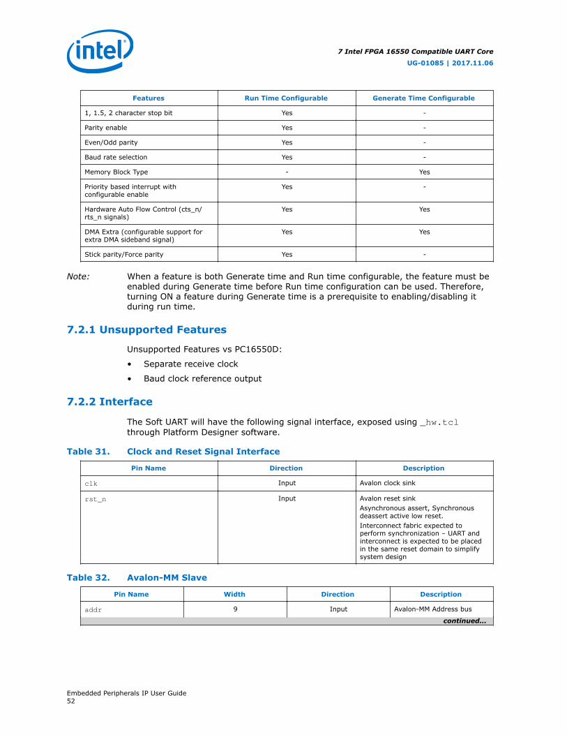
Features Run Time Configurable Generate Time Configurable
1, 1.5, 2 character stop bit Yes -
Parity enable Yes -
Even/Odd parity Yes -
Baud rate selection Yes -
Memory Block Type - Yes
Priority based interrupt withconfigurable enable
Yes -
Hardware Auto Flow Control (cts_n/rts_n signals)
Yes Yes
DMA Extra (configurable support forextra DMA sideband signal)
Yes Yes
Stick parity/Force parity Yes -
Note: When a feature is both Generate time and Run time configurable, the feature must beenabled during Generate time before Run time configuration can be used. Therefore,turning ON a feature during Generate time is a prerequisite to enabling/disabling itduring run time.
7.2.1 Unsupported Features
Unsupported Features vs PC16550D:
• Separate receive clock
• Baud clock reference output
7.2.2 Interface
The Soft UART will have the following signal interface, exposed using _hw.tclthrough Platform Designer software.
Table 31. Clock and Reset Signal Interface
Pin Name Direction Description
clk Input Avalon clock sink
rst_n Input Avalon reset sinkAsynchronous assert, Synchronousdeassert active low reset.Interconnect fabric expected toperform synchronization – UART andinterconnect is expected to be placedin the same reset domain to simplifysystem design
Table 32. Avalon-MM Slave
Pin Name Width Direction Description
addr 9 Input Avalon-MM Address bus
continued...
7 Intel FPGA 16550 Compatible UART Core
UG-01085 | 2017.11.06
Embedded Peripherals IP User Guide52

Pin Name Width Direction Description
Highest addressable byteaddress is 0x118 so a 9-bitwidth is required
read Input Avalon-MM Read indication
readdata 32 Output Avalon-MM Read DataResponse from the slave
write Input Avalon-MM Write indication
writedata 32 Input Avalon-MM Write Data
Table 33. Interrupt Interface
Pin Name Direction Description
intr Output Interrupt signal
Table 34. Flow Control
Pin Name Direction Description
sin Input Serial Input from external link.
sout Output Serial Output to external link.
sout_oe Output Output enable for Serial Output to external link.sout_oe signal will be high when the UART is transmittingand low when the UART is IDLE.
Table 35. Modem Control and Status
Pin Name Direction Description
cts_n Input Clear to Send
rts_n Output Request to Send
dsr_n Input Data Set Ready
dcd_n Input Data Carrier Detect
ri_n Input Ring Indicator
dtr_n Output Data Terminal Ready
out1_n Output User Designated Output1
out2_n Output User Designated Output2
Table 36. DMA Sideband Signals
Pin Name Direction Description
dma_tx_ack_n Input TX DMA acknowledge
dma_rx_ack_n Input RX DMA acknowledge
dma_tx_req_n Output TX DMA request
dma_rx_req_n Output RX DMA request
dma_tx_single_n Output TX DMA single request
dma_rx_single_n Output RX DMA single request
7 Intel FPGA 16550 Compatible UART Core
UG-01085 | 2017.11.06
Embedded Peripherals IP User Guide53
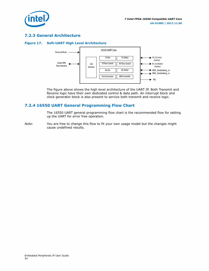
7.2.3 General Architecture
Figure 17. Soft-UART High Level Architecture
TX Fifo TX Shifter
TX Flow Control RX Flow Control
RX ShifterRX Fifo
Clock Generator DMA Controller
CSRInterface
16550 UART CoreClock and Reset
Avalon MM Slave Interface
RS-232 Serial Interface
RS-232 Modem Interface
DMA_Handshaking_txDMA_Handshaking_rx
IRQ
The figure above shows the high level architecture of the UART IP. Both Transmit andReceive logic have their own dedicated control & data path. An interrupt block andclock generator block is also present to service both transmit and receive logic.
7.2.4 16550 UART General Programming Flow Chart
The 16550 UART general programming flow chart is the recommended flow for settingup the UART for error free operation.
Note: You are free to change this flow to fit your own usage model but the changes mightcause undefined results.
7 Intel FPGA 16550 Compatible UART Core
UG-01085 | 2017.11.06
Embedded Peripherals IP User Guide54
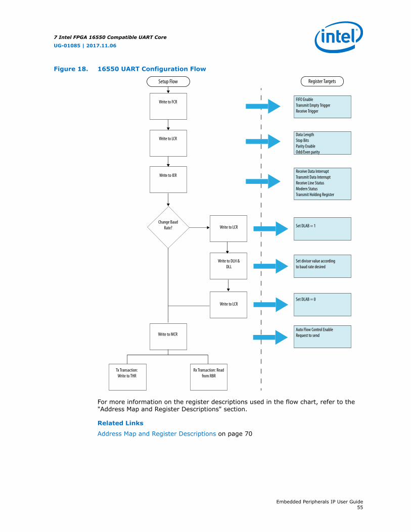
Figure 18. 16550 UART Configuration Flow
Setup Flow Register Targets
Write to FCR
Write to LCR
Write to IER
Write to LCR
Write to DLH & DLL
Write to LCR
Change Baud Rate?
Write to MCR
Tx Transaction: Write to THR
Rx Transaction: Read from RBR
FIFO EnableTransmit Empty TriggerReceive Trigger
Data LengthStop BitsParity EnableOdd/Even parity
Receive Data InterruptTransmit Data InterruptReceive Line StatusModern StatusTransmit Holding Register
Set DLAB = 1
Set divisor value according to baud rate desired
Set DLAB = 0
Auto Flow Control EnableRequest to send
For more information on the register descriptions used in the flow chart, refer to the"Address Map and Register Descriptions" section.
Related Links
Address Map and Register Descriptions on page 70
7 Intel FPGA 16550 Compatible UART Core
UG-01085 | 2017.11.06
Embedded Peripherals IP User Guide55
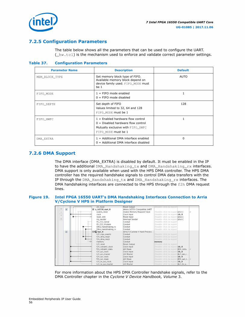
7.2.5 Configuration Parameters
The table below shows all the parameters that can be used to configure the UART.(_hw.tcl) is the mechanism used to enforce and validate correct parameter settings.
Table 37. Configuration Parameters
Parameter Name Description Default
MEM_BLOCK_TYPE Set memory block type of FIFO.Available memory block depend ondevice family used. FIFO_MODE mustbe 1
AUTO
FIFO_MODE 1 = FIFO mode enabled0 = FIFO mode disabled
1
FIFO_DEPTH Set depth of FIFOValues limited to 32, 64 and 128FIFO_MODE must be 1
128
FIFO_HWFC 1 = Enabled hardware flow control0 = Disabled hardware flow controlMutually exclusive with FIFO_SWFCFIFO_MODE must be 1
1
DMA_EXTRA 1 = Additional DMA interface enabled0 = Additional DMA interface disabled
0
7.2.6 DMA Support
The DMA interface (DMA_EXTRA) is disabled by default. It must be enabled in the IPto have the additional DMA_Handshaking_tx and DMA_Handshaking_rx interfaces.DMA support is only available when used with the HPS DMA controller. The HPS DMAcontroller has the required handshake signals to control DMA data transfers with theIP through the DMA_Handshaking_tx and DMA_Handshaking_rx interfaces. TheDMA handshaking interfaces are connected to the HPS through the f2h DMA requestlines.
Figure 19. Intel FPGA 16550 UART's DMA Handshaking Interfaces Connection to ArriaV/Cyclone V HPS in Platform Designer
For more information about the HPS DMA Controller handshake signals, refer to theDMA Controller chapter in the Cyclone V Device Handbook, Volume 3.
7 Intel FPGA 16550 Compatible UART Core
UG-01085 | 2017.11.06
Embedded Peripherals IP User Guide56
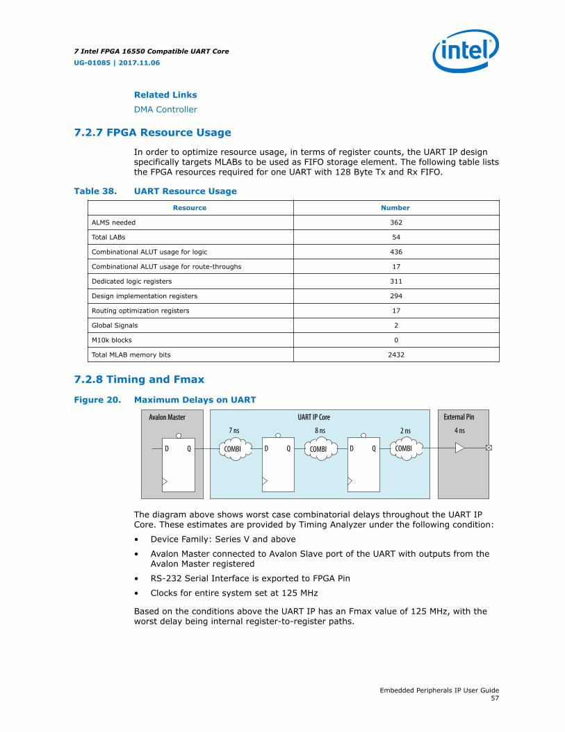
Related Links
DMA Controller
7.2.7 FPGA Resource Usage
In order to optimize resource usage, in terms of register counts, the UART IP designspecifically targets MLABs to be used as FIFO storage element. The following table liststhe FPGA resources required for one UART with 128 Byte Tx and Rx FIFO.
Table 38. UART Resource Usage
Resource Number
ALMS needed 362
Total LABs 54
Combinational ALUT usage for logic 436
Combinational ALUT usage for route-throughs 17
Dedicated logic registers 311
Design implementation registers 294
Routing optimization registers 17
Global Signals 2
M10k blocks 0
Total MLAB memory bits 2432
7.2.8 Timing and Fmax
Figure 20. Maximum Delays on UART
External PinUART IP Core
D Q
Avalon Master
D Q D Q
4 ns2 ns8 ns7 ns
COMBI COMBI COMBI
The diagram above shows worst case combinatorial delays throughout the UART IPCore. These estimates are provided by Timing Analyzer under the following condition:
• Device Family: Series V and above
• Avalon Master connected to Avalon Slave port of the UART with outputs from theAvalon Master registered
• RS-232 Serial Interface is exported to FPGA Pin
• Clocks for entire system set at 125 MHz
Based on the conditions above the UART IP has an Fmax value of 125 MHz, with theworst delay being internal register-to-register paths.
7 Intel FPGA 16550 Compatible UART Core
UG-01085 | 2017.11.06
Embedded Peripherals IP User Guide57

The UART has combinatorial logic on both the Input and Output side, with system levelimplications on the Input side.
The Input side combinatorial logic (with 7ns delay) goes through the Avalon addressdecode logic, to the Read data output registers. It is therefore recommended thatMasters connected to the UART IP register their output signals.
The Output side combinatorial logic (with 2ns delay) goes through the RS-232 SerialOutput. There should not be any concern on the output side delays though – as it isnot a single cycle path. Using the highest clock divider value of 1, the serial outputonly toggles once every 16 clocks. This naturally gives a 16 clock multi-cycle path onthe output side. Furthermore, divider of 1 is an unlikely system, if the UART is clockedat 125 MHz, the resulting baud rate would be 7.81 Mbps.
7.2.9 Avalon-MM Slave
The Avalon-MM Slave has the following configuration:
Table 39. Avalon-MM Slave Configuration
Feature Configuration
Bus Width 32-bit
Burst Support No burst support. Interconnect is expected to handle burstconversion
Fixed read and write wait time 0 cycles
Fixed read latency 1 cycle
Fixed write latency 0 cycles
Lock support No
Note: The Avalon-MM interface is intended to be a thin, low latency layer on top of theregisters.
7.2.9.1 Read behavior
Figure 21. Reading UART over Avalon-MM
addr1 addrF addrF addrF
data1 data2 data3 data4
addr
readreaddata
Polling Status Reading fromRX FIFO
0 1 2 3 4 5 6 7 8 9
Reads are expected to have 2 types of behavior:
• When status registers are being polled, Reads are expected to be done in singles
• When data needs to be read out from the Rx FIFO, Reads are expected as back-to-back cycles to the same address (these back-to-back reads are likely generated asFixed Bursts in AXI – but translated into INCR with length of 1 by FPGAinterconnect)
7 Intel FPGA 16550 Compatible UART Core
UG-01085 | 2017.11.06
Embedded Peripherals IP User Guide58
7.2.9.2 Write behavior
Figure 22. Writing to UART over Avalon-MM
addr1 addrF addrF addrF
data1 data2 data3 data4
addr
readreaddata
Configuration Writing toTX FIFO
0 1 2 3 4 5 6 7 8 9
Writes to the UART are expected as singles during setup phase of any transaction andas back-to-back writes to the same address when the Tx FIFO needs to be filled.
7.2.10 Overrun/Underrun Conditions
Consistent with UART implementation in PC16550D, the soft UART will not implementoverrun or underrun prevention on the Avalon-MM interface.
Preventing overruns and underruns on the Avalon-MM interface by back-pressuring apending transaction may cause more harm than good as the interconnect can be heldup by the far slower UART.
7.2.10.1 Overrun
On receive path, interrupts can be triggered (when enabled) when overrun occurs. InFIFO-less mode, overrun happens when an existing character in the receive buffer isoverwritten by a new character before it can be read. In FIFO mode, overrun happenswhen the FIFO is full and a complete character arrives at the receive buffer.
On transmit path, software driver is expected to know the Tx FIFO depth and notoverrun the UART.
7.2.10.2 Receive Overrun Behavior
When receive overrun does happen, the Soft-UART handles it differently depending onFIFO mode. With FIFO enabled, the newly receive data at the shift register is lost.With FIFO disabled, the newly received data from the shift register is written onto theReceive Buffer. The existing data in the Receive Buffer is overwritten. This is consistentwith published PC16550D UART behavior.
7.2.10.3 Transmit Overrun Behavior
When the host CPU forcefully triggers a transmit Overrun, the Soft-UART handles itdifferently depending on FIFO mode. With FIFO enabled, the newly written data is lost.With FIFO disabled, the newly written data will overwrite the existing data in theTransmit Holding Register.
7.2.10.4 Underrun
No mechanisms exist to detect or prevent underrun.
7 Intel FPGA 16550 Compatible UART Core
UG-01085 | 2017.11.06
Embedded Peripherals IP User Guide59

On transmit path, an interrupts, when enabled, can be generated when the transmitholding register is empty or when the transmit FIFO is below a programmed level.
On receive path, the software driver is expected to read from the UART receive buffer(FIFO-less) or the (Rx FIFO) based on interrupts, when enabled, or status registersindicating presence of receive data (Data Ready bit, LSR[0]). If reads to ReceiveBuffer Register is triggered with data ready register being zero, undefined read data isreturned.
7.2.11 Hardware Auto Flow-Control
Hardware based auto flow-control uses 2 signals (cts_n & rts_n) from the ModemControl/Status group. With Hardware auto flow-control disabled, these signals willdirectly drive the Modem Status register (cts_n) or be driven by the Modem Controlregister (rts_n).
With auto flow-control enabled, these signals perform flow-control duty with anotherUART at the other end.
The cts_n input is, when active (low state), will allow the Tx FIFO to send data tothe transmit buffer. When cts_n is inactive (high state), the Tx FIFO stops sendingdata to the transmit buffer. cts_n is expected to be connected to the rts_n outputof the other UART.
The rts_n output will go active (low state), when the Rx FIFO is empty, signaling tothe opposite UART that it is ready for data. The rts_n output goes inactive (highstate) when the Rx FIFO level is reached, signaling to the opposite UART that the FIFOis about to go full and it should stop transmitting.
Due to the delays within the UART logic, one additional character may be transmittedafter cts_n is sampled active low. For the same reason, the Rx FIFO willaccommodate up to 1 additional character after asserting rts_n (this is allowedbecause Rx FIFO trigger level is at worst, two entries from being truly full). Both areobserved to prevent overflow/underflow between UARTs.
Figure 23. Hardware Auto Flow-Control Between two UARTs
TXFIFO
Transmit Buffer
Flow Control
RXFIFO
Receive Buffer
Flow Control
RXFIFO
Receive Buffer
Flow Control
TXFIFO
Transmit Buffer
Flow Control
sout
cts_n
sin
rts_n
sin
rts_n
sout
cts_n
UART 1 UART 2
7 Intel FPGA 16550 Compatible UART Core
UG-01085 | 2017.11.06
Embedded Peripherals IP User Guide60

7.2.12 Clock and Baud Rate Selection
The Soft-UART supports only one clock. The same clock is used on the Avalon-MMinterface and will be used to generate the baud clock that drives the serial UARTinterface.
The baud rate on the serial UART interface is set using the following equation:
Baud Rate = Clock/(16 x Divisor)
The table below shows how several typical baud rates can be achieved byprogramming the divisor values in Divisor Latch High and Divisor Latch Low register.
Table 40. UART Clock Frequency, Divider value and Baud Rate Relationship
18.432 MHz 24 MHz 50 MHz
Baud Rate Divisor for 16xclock
% Error (baud) Divisor for 16xclock
% Error (baud) Divisor for 16xclock
% Error (baud)
9,600 120 0.00% 156 0.16% 326 -0.15%
38,400 30 0.00% 39 0.16% 81 0.47%
115,200 10 0.00% 13 0.16% 27 0.47%
7.3 Software Programming Model
7.3.1 Overview
The following describes the programming model for the Intel FPGA compatible 16550Soft-UART.
7.3.2 Supported Features
For the following features, the 16550 Soft-UART HAL driver can be configurable in runtime or generate time. For run-time configuration, users can use“altera_16550_uart_config” API . Generate time is during Platform Designergeneration, that is to say once FIFO Depth is selected the depth for the FIFO can’t bechange anymore.
Table 41. Supported Features
Features Run Time Generate Time
FIFO/ FIFO-less mode Yes Yes
FIFO Depth - Yes
Programmable Tx/Rx FIFO Threshold Yes -
5-9 bit character length Yes -
1, 1.5, 2 character stop bit Yes -
Parity enable Yes -
Even/Odd parity Yes -
continued...
7 Intel FPGA 16550 Compatible UART Core
UG-01085 | 2017.11.06
Embedded Peripherals IP User Guide61

Features Run Time Generate Time
Stick parity Yes -
Baud rate selection Yes -
Priority based interrupt withconfigurable enable
Yes -
Hardware Auto Flow Control Yes Yes
7.3.3 Unsupported Features
The 16550 UART driver does not support Software flow control.
7.3.4 Configuration
The figure below shows the Platform Designer setup on the 16550 Soft-UART's FIFODepth
Figure 24. Platform Designer Setting to Configure FIFO Depth
7.3.5 16550 UART API
7.3.5.1 Public APIs
Table 42. altera_16550_uart_open
Prototype: altera_16550_uart_dev * altera_16550_uart_open(constchar* name);
Include: <altera_16550_uart.h>
Parameters: name—the 16550 UART device name to open.
Returns: Pointer to 16550 UART or NULL if fail to open
Description Open 16550 UART device.
Table 43. altera_16550_uart_close
Prototype: void alt_16550_uart_close (const char* name)
Include: <altera_16550_uart.h>
continued...
7 Intel FPGA 16550 Compatible UART Core
UG-01085 | 2017.11.06
Embedded Peripherals IP User Guide62
Parameters: name—the 16550 UART device name to close.
Returns: None
Description: Closes 16550 UART device.
Table 44. alt_16550_uart_read
Prototype: alt_u32 altera_16550_uart_read(altera_16550_uart_dev*dev, const char * ptr, alt_u16 len, alt_u16 flags);
Include: <altera_16550_uart.h>
Parameters: dev - The UART deviceptr – destination addresslen – maximum length of the dataflags – for indicating blocking/non-blocking access for single/multi threaded
Returns: Number of bytes read
Description: Read data to the UART receiver buffer. UART required to be ina known settings prior executing this function
Table 45. alt_16550_uart_write
Prototype: alt_u32 alt_16550_uart_write(altera_16550_uart_dev* dev,const char * ptr, alt_u16 flags, int len);
Include: <altera_16550_uart.h>
Parameters: dev - The UART deviceptr – source addresslen – maximum length of the dataflags – for indicating blocking/non-blocking access for single/multi threaded
Returns: Number of bytes written
Description: Writes data to the UART transmitter buffer. UART required tobe in a known settings prior executing this function
Table 46. alt_16550_uart_config
Prototype: alt_u32 alt_16550_uart_config(altera_16550_uart_dev* dev,UartConfig *config);
Include: dev - The UART device
Parameters: config – UART configuration structure to configure UART(refer to UART device structure
Returns: Return 0 for success otherwise fail
Description: Configure UART per user input before initiating read or Write
7.3.5.2 Private APIs
Table 47. alt_16550_irq
Prototype: static void altera_16550_uart_irq (void* context)
Include: <altera_16550_uart.h>
continued...
7 Intel FPGA 16550 Compatible UART Core
UG-01085 | 2017.11.06
Embedded Peripherals IP User Guide63
Parameters: context – device of the UART
Returns: none
Description: Interrupt handler to process UART interrupts to processreceiver/transmit interrupts.
Table 48. alt_16550_uart_rxirq
Prototype: static void altera_16550_uart_rxirq(altera_16550_uart_dev* dev, alt_u32
Include: <altera_16550_uart.h>
Parameters: context – device of the UART
Returns: none
Description: Process a receive interrupt. It transfers the incomingcharacter into the receiver circular buffer, and sets theappropriate flags to indicate that there is data ready to beprocessed.
Table 49. alt_16550_uart_txirq
Prototype: static void altera_16550_uart_txirq(altera_16550_uart_dev* dev, alt_u32 status
Include: <altera_16550_uart.h>
Parameters: context – device of the UART
Returns: none
Description: Process a transmit interrupt. It transfers data from thetransmit buffer to the device, and sets the appropriate flagsto indicate that there is data ready to be processed.
7.3.5.3 UART Device Structure
Example 1. UART Device Structure 1
typedef enum stopbit { STOPB_1 = 0,STOPB_2 } StopBit;typedef enum paritybit { ODD_PARITY = 0, EVEN_PARITY, MARK_PARITY, SPACE_PARITY, NO_PARITY } ParityBit;typedef enum databit { CS_5 = 0, CS_6, CS_7, CS_8, CS_9 = 256} DataBit;typedef enum baud{BR9600 = B9600,BR19200 = B19200,BR38400 = B38400,BR57600 = B57600,BR115200 = B115200} Baud;typedef enum rx_fifo_level_e { RXONECHAR = 0, RXQUARTER, RXHALF, RXFULL } Rx_FifoLvl;typedef enum tx_fifo_level_e { TXEMPTY = 0, TXTWOCHAR, TXQUARTER, TXHALF } Tx_FifoLvl;typedef struct uart_config_s{StopBit stop_bit;ParityBit parity_bit;DataBit data_bit;Baud baudrate;alt_u32 fifo_mode;Rx_FifoLvl rx_fifo_level;
7 Intel FPGA 16550 Compatible UART Core
UG-01085 | 2017.11.06
Embedded Peripherals IP User Guide64

Tx_FifoLvl tx_fifo_level;alt_u32 hwfc;} UartConfig;
Example 2. UART Device Structure 2
typedef struct altera_16550_uart_state_s{ alt_dev dev; void* base; /* The base address of the device */ alt_u32 clock; alt_u32 hwfifomode; alt_u32 ctrl; /* Shadow value of the LSR register */ volatile alt_u32 rx_start; /* Start of the pending receive data */ volatile alt_u32 rx_end; /* End of the pending receive data */ volatile alt_u32 tx_start; /* Start of the pending transmit data */ volatile alt_u32 tx_end; /* End of the pending transmit data */ alt_u32 freq; /* Current clock freq rate */ UartConfig config; /* Uart setting */ #ifdef ALTERA_16550_UART_USE_IOCTL struct termios termios; #endif alt_u32 flags; /* Configuration flags */ ALT_FLAG_GRP (events) /* Event flags used for * foreground/background in mult-threaded * mode */ ALT_SEM (read_lock) /* Semaphore used to control access to the * read buffer in multi-threaded mode */ ALT_SEM (write_lock) /* Semaphore used to control access to the * write buffer in multi-threaded mode */ volatile wchar_t rx_buf[ALT_16550_UART_BUF_LEN]; /* The receive buffer */ volatile wchar_t tx_buf[ALT_16550_UART_BUF_LEN]; /* The transmit buffer */ line_status_reg line_status; /* line register status for the current read byte data of RBR or data at the top of FIFO*/ alt_u8 error_ignore; /* received data will be discarded for the current read byte data of RBR or data at the top of FIFO if pe, fe and bi errors detected after error_ignore is set to '0' */ } altera_16550_uart_state;
7 Intel FPGA 16550 Compatible UART Core
UG-01085 | 2017.11.06
Embedded Peripherals IP User Guide65

7.3.6 Driver Examples
Below is a simple test program to verify that the Intel FPGA 16550 UART driversupport is functional.
The test reads, validates, and writes a modified baud rate, data bits, stop bits, paritybits to the UART before attempting to write a character stream to it from UART0 toUART1 and vice verse (ping pong test). This also tests the FIFO and FIFO-less modeas well as the HW flow control to ensure the IP is functioning for FIFO and HWFC.
Prerequisites needed before running test:
• An instance of UART named "uart0" and another instance UART named "uart1".
• Both UARTs need to be connected in loopback in Intel Quartus Prime.
Additional coverage:
• Non-blocking UART support
• UART HAL driver
• HAL open/write support
The test will print "PASS: . . ." from the UART to indicate success.
Example 3. Verifying Intel FPGA 16550 UART Driver Support functionality
#include <stdio.h>#include <stdlib.h>#include <sys/ioctl.h>#include <sys/termios.h>#include <fcntl.h>#include <string.h>#include <unistd.h>#include <sys/time.h>#include <time.h>#include "system.h"#include "altera_16550_uart.h"#include "altera_16550_uart_regs.h"
#define ERROR -1#define SUCCESS 0#define MOCK_UART#define BUFSIZE 512char TXMessage[BUFSIZE] = "Hello World";char RXMessage[BUFSIZE] = "";
int UARTDefaultConfig(UartConfig *Config){ Config->stop_bit = STOPB_1; Config->parity_bit = NO_PARITY; Config->data_bit = CS_8; Config->baudrate = BR115200; Config->fifo_mode = 0; Config->hwfc = 0; Config->rx_fifo_level= RXFULL; Config->tx_fifo_level= TXEMPTY; return 0;}
int UARTBaudRateTest(){ UartConfig *UART0_Config = malloc(1*sizeof(UartConfig)); UartConfig *UART1_Config = malloc(1*sizeof(UartConfig));
int i=0, j=0, direction=0, Match=0; const int nBaud = 5;
7 Intel FPGA 16550 Compatible UART Core
UG-01085 | 2017.11.06
Embedded Peripherals IP User Guide66
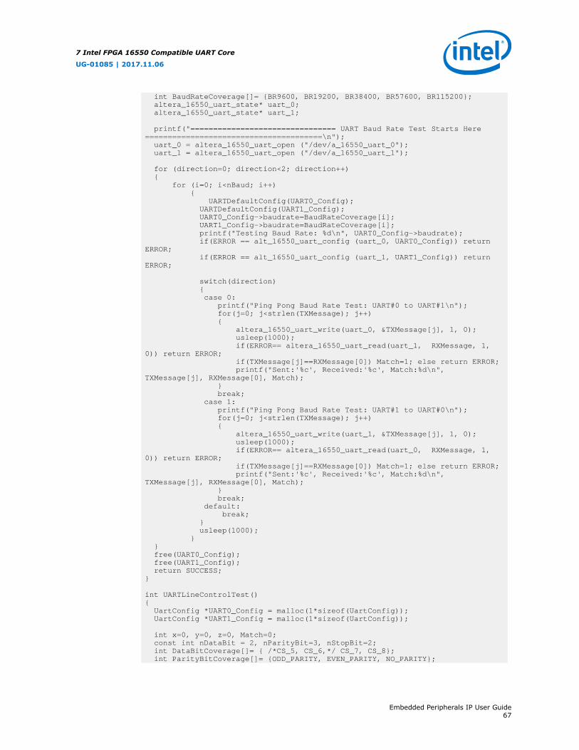
int BaudRateCoverage[]= {BR9600, BR19200, BR38400, BR57600, BR115200}; altera_16550_uart_state* uart_0; altera_16550_uart_state* uart_1;
printf("================================ UART Baud Rate Test Starts Here =======================================\n"); uart_0 = altera_16550_uart_open ("/dev/a_16550_uart_0"); uart_1 = altera_16550_uart_open ("/dev/a_16550_uart_1");
for (direction=0; direction<2; direction++) { for (i=0; i<nBaud; i++) { UARTDefaultConfig(UART0_Config); UARTDefaultConfig(UART1_Config); UART0_Config->baudrate=BaudRateCoverage[i]; UART1_Config->baudrate=BaudRateCoverage[i]; printf("Testing Baud Rate: %d\n", UART0_Config->baudrate); if(ERROR == alt_16550_uart_config (uart_0, UART0_Config)) return ERROR; if(ERROR == alt_16550_uart_config (uart_1, UART1_Config)) return ERROR;
switch(direction) { case 0: printf("Ping Pong Baud Rate Test: UART#0 to UART#1\n"); for(j=0; j<strlen(TXMessage); j++) { altera_16550_uart_write(uart_0, &TXMessage[j], 1, 0); usleep(1000); if(ERROR== altera_16550_uart_read(uart_1, RXMessage, 1, 0)) return ERROR; if(TXMessage[j]==RXMessage[0]) Match=1; else return ERROR; printf("Sent:'%c', Received:'%c', Match:%d\n", TXMessage[j], RXMessage[0], Match); } break; case 1: printf("Ping Pong Baud Rate Test: UART#1 to UART#0\n"); for(j=0; j<strlen(TXMessage); j++) { altera_16550_uart_write(uart_1, &TXMessage[j], 1, 0); usleep(1000); if(ERROR== altera_16550_uart_read(uart_0, RXMessage, 1, 0)) return ERROR; if(TXMessage[j]==RXMessage[0]) Match=1; else return ERROR; printf("Sent:'%c', Received:'%c', Match:%d\n", TXMessage[j], RXMessage[0], Match); } break; default: break; } usleep(1000); } } free(UART0_Config); free(UART1_Config); return SUCCESS;}
int UARTLineControlTest(){ UartConfig *UART0_Config = malloc(1*sizeof(UartConfig)); UartConfig *UART1_Config = malloc(1*sizeof(UartConfig));
int x=0, y=0, z=0, Match=0; const int nDataBit = 2, nParityBit=3, nStopBit=2; int DataBitCoverage[]= { /*CS_5, CS_6,*/ CS_7, CS_8}; int ParityBitCoverage[]= {ODD_PARITY, EVEN_PARITY, NO_PARITY};
7 Intel FPGA 16550 Compatible UART Core
UG-01085 | 2017.11.06
Embedded Peripherals IP User Guide67
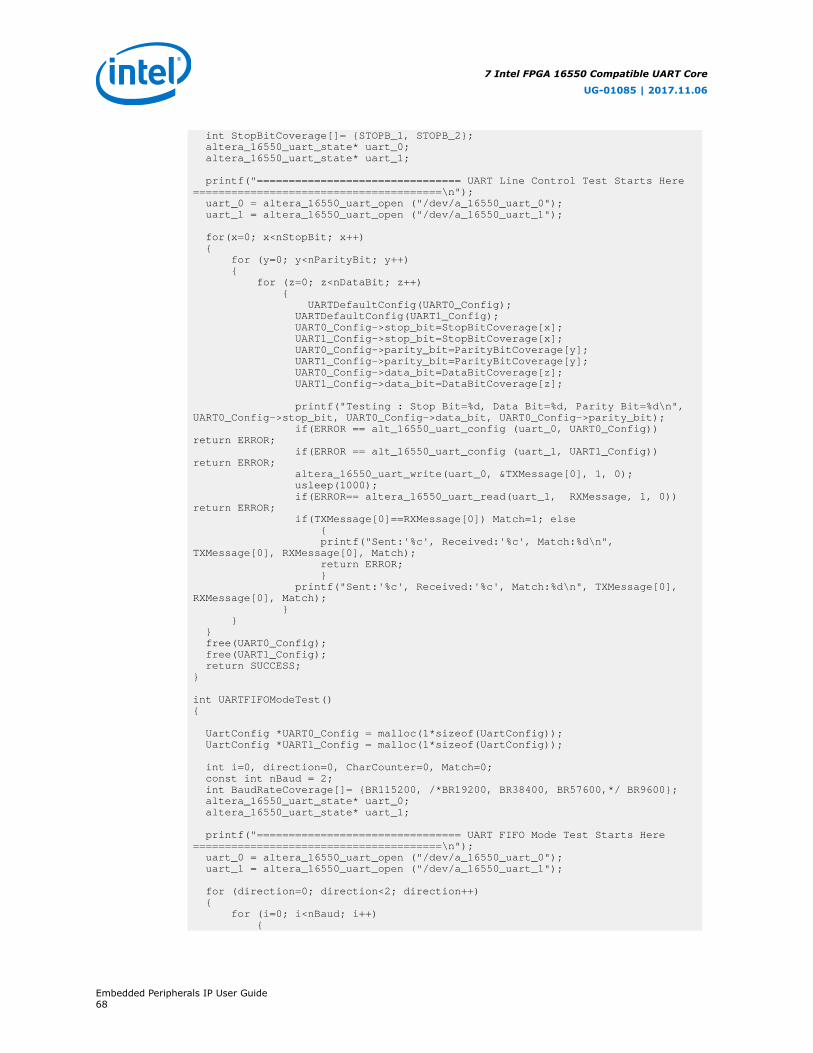
int StopBitCoverage[]= {STOPB_1, STOPB_2}; altera_16550_uart_state* uart_0; altera_16550_uart_state* uart_1;
printf("================================ UART Line Control Test Starts Here =======================================\n"); uart_0 = altera_16550_uart_open ("/dev/a_16550_uart_0"); uart_1 = altera_16550_uart_open ("/dev/a_16550_uart_1");
for(x=0; x<nStopBit; x++) { for (y=0; y<nParityBit; y++) { for (z=0; z<nDataBit; z++) { UARTDefaultConfig(UART0_Config); UARTDefaultConfig(UART1_Config); UART0_Config->stop_bit=StopBitCoverage[x]; UART1_Config->stop_bit=StopBitCoverage[x]; UART0_Config->parity_bit=ParityBitCoverage[y]; UART1_Config->parity_bit=ParityBitCoverage[y]; UART0_Config->data_bit=DataBitCoverage[z]; UART1_Config->data_bit=DataBitCoverage[z];
printf("Testing : Stop Bit=%d, Data Bit=%d, Parity Bit=%d\n", UART0_Config->stop_bit, UART0_Config->data_bit, UART0_Config->parity_bit); if(ERROR == alt_16550_uart_config (uart_0, UART0_Config)) return ERROR; if(ERROR == alt_16550_uart_config (uart_1, UART1_Config)) return ERROR; altera_16550_uart_write(uart_0, &TXMessage[0], 1, 0); usleep(1000); if(ERROR== altera_16550_uart_read(uart_1, RXMessage, 1, 0)) return ERROR; if(TXMessage[0]==RXMessage[0]) Match=1; else { printf("Sent:'%c', Received:'%c', Match:%d\n", TXMessage[0], RXMessage[0], Match); return ERROR; } printf("Sent:'%c', Received:'%c', Match:%d\n", TXMessage[0], RXMessage[0], Match); } } } free(UART0_Config); free(UART1_Config); return SUCCESS;}
int UARTFIFOModeTest(){
UartConfig *UART0_Config = malloc(1*sizeof(UartConfig)); UartConfig *UART1_Config = malloc(1*sizeof(UartConfig));
int i=0, direction=0, CharCounter=0, Match=0; const int nBaud = 2; int BaudRateCoverage[]= {BR115200, /*BR19200, BR38400, BR57600,*/ BR9600}; altera_16550_uart_state* uart_0; altera_16550_uart_state* uart_1;
printf("================================ UART FIFO Mode Test Starts Here =======================================\n"); uart_0 = altera_16550_uart_open ("/dev/a_16550_uart_0"); uart_1 = altera_16550_uart_open ("/dev/a_16550_uart_1");
for (direction=0; direction<2; direction++) { for (i=0; i<nBaud; i++) {
7 Intel FPGA 16550 Compatible UART Core
UG-01085 | 2017.11.06
Embedded Peripherals IP User Guide68

UARTDefaultConfig(UART0_Config); UARTDefaultConfig(UART1_Config); UART0_Config->baudrate=BaudRateCoverage[i]; UART1_Config->baudrate=BaudRateCoverage[i]; UART0_Config->fifo_mode = 1; UART1_Config->fifo_mode = 1; UART0_Config->hwfc = 0; UART1_Config->hwfc = 0; if(ERROR == alt_16550_uart_config (uart_0, UART0_Config)) return ERROR; if(ERROR == alt_16550_uart_config (uart_1, UART1_Config)) return ERROR; printf("Testing Baud Rate: %d\n", UART0_Config->baudrate);
switch(direction) { case 0: printf("Ping Pong FIFO Test: UART#0 to UART#1\n"); CharCounter=altera_16550_uart_write(uart_0, &TXMessage, strlen(TXMessage), 0); //usleep(50000); if(ERROR== altera_16550_uart_read(uart_1, RXMessage, strlen(TXMessage), 0)) return ERROR; if(strcmp(TXMessage, RXMessage)==0) Match=1; else Match=0; printf("Sent:'%s' CharCount:%d, Received:'%s' CharCount:%d, Match:%d\n", TXMessage, CharCounter, RXMessage, strlen(RXMessage), Match); if(Match==0) return ERROR; break; case 1: printf("Ping Pong FIFO Test: UART#1 to UART#0\n"); CharCounter=altera_16550_uart_write(uart_1, &TXMessage, strlen(TXMessage), 0); //usleep(50000); if(ERROR== altera_16550_uart_read(uart_0, RXMessage, strlen(TXMessage), 0)) return ERROR; if(strcmp(TXMessage, RXMessage)==0) Match=1; else Match=0; printf("Sent:'%s' CharCount:%d, Received:'%s' CharCount:%d, Match:%d\n", TXMessage, CharCounter, RXMessage, strlen(RXMessage), Match); if(Match==0) return ERROR; break; default: break; } //usleep(100000); } } free(UART0_Config); free(UART1_Config); return SUCCESS;}
int main(){ int result=0;
result = UARTBaudRateTest(); if(result==ERROR) { printf("UARTBaudRateTest FAILED\n"); return ERROR; }
result = UARTLineControlTest(); if(result==ERROR) { printf("UARTLineControlTest FAILED\n"); return ERROR; }
result = UARTFIFOModeTest(); if(result==ERROR)
7 Intel FPGA 16550 Compatible UART Core
UG-01085 | 2017.11.06
Embedded Peripherals IP User Guide69
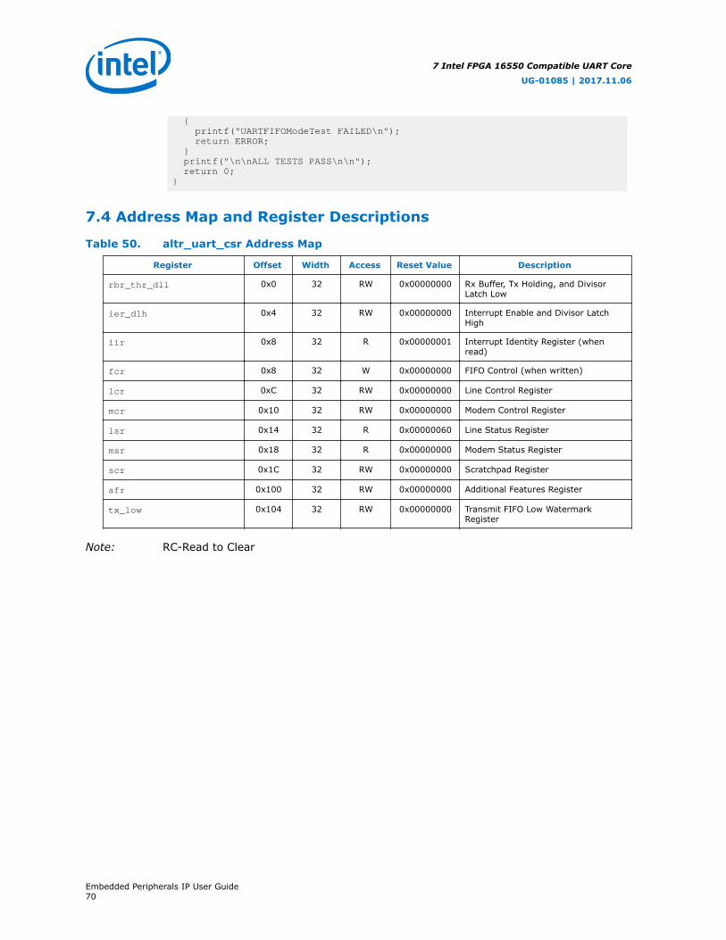
{ printf("UARTFIFOModeTest FAILED\n"); return ERROR; } printf("\n\nALL TESTS PASS\n\n"); return 0;}
7.4 Address Map and Register Descriptions
Table 50. altr_uart_csr Address Map
Register Offset Width Access Reset Value Description
rbr_thr_dll 0x0 32 RW 0x00000000 Rx Buffer, Tx Holding, and DivisorLatch Low
ier_dlh 0x4 32 RW 0x00000000 Interrupt Enable and Divisor LatchHigh
iir 0x8 32 R 0x00000001 Interrupt Identity Register (whenread)
fcr 0x8 32 W 0x00000000 FIFO Control (when written)
lcr 0xC 32 RW 0x00000000 Line Control Register
mcr 0x10 32 RW 0x00000000 Modem Control Register
lsr 0x14 32 R 0x00000060 Line Status Register
msr 0x18 32 R 0x00000000 Modem Status Register
scr 0x1C 32 RW 0x00000000 Scratchpad Register
afr 0x100 32 RW 0x00000000 Additional Features Register
tx_low 0x104 32 RW 0x00000000 Transmit FIFO Low WatermarkRegister
Note: RC-Read to Clear
7 Intel FPGA 16550 Compatible UART Core
UG-01085 | 2017.11.06
Embedded Peripherals IP User Guide70
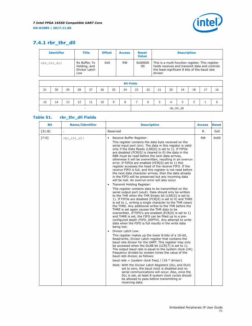
7.4.1 rbr_thr_dll
Identifier Title Offset Access ResetValue
Description
rbr_thr_dll Rx Buffer, TxHolding, andDivisor LatchLow
0x0 RW 0x0000000
This is a multi-function register. This registerholds receives and transmit data and controlsthe least-signficant 8 bits of the baud ratedivisor.
Bit Fields
31 30 29 28 27 26 25 24 23 22 21 20 19 18 17 16
-
15 14 13 12 11 10 9 8 7 6 5 4 3 2 1 0
- rbr_thr_dll
Table 51. rbr_thr_dll Fields
Bit Name/Identifier Description Access Reset
[31:8] - Reserved R 0x0
[7:0] rbr_thr_dll • Receive Buffer Register:This register contains the data byte received on theserial input port (sin). The data in this register is validonly if the Data Ready (LSR[0] is set to 1). If FIFOsare disabled (FCR[0] is cleared to 0) the data in theRBR must be read before the next data arrives,otherwise it will be overwritten, resulting in an overrunerror. If FIFOs are enabled (FCR[0] set to 1) thisregister accesses the head of the receive FIFO. If thereceive FIFO is full, and this register is not read beforethe next data character arrives, then the data alreadyin the FIFO will be preserved but any incoming datawill be lost. An overrun error will also occur.
• Transmit Holding Register:This register contains data to be transmitted on theserial output port (sout). Data should only be writtento the THR when the THR Empty bit (LSR[5] is set to1). If FIFOs are disabled (FCR[0] is set to 0) and THREis set to 1, writing a single character to the THR clearsthe THRE. Any additional writes to the THR before theTHRE is set again causes the THR data to beoverwritten. If FIFO's are enabled (FCR[0] is set to 1)and THRE is set, the FIFO can be filled up to a pre-configured depth (FIFO_DEPTH). Any attempt to writedata when the FIFO is full results in the write databeing lost.
• Divisor Latch Low:This register makes up the lower 8-bits of a 16-bit,Read/write, Divisor Latch register that contains thebaud rate divisor for the UART. This register may onlybe accessed when the DLAB bit (LCR[7] is set to 1).The output baud rate is equal to the system clock (clk)frequency divided by sixteen times the value of thebaud rate divisor, as follows:baud rate = (system clock freq) / (16 * divisor)Note: With the Divisor Latch Registers (DLL and DLH)
set to zero, the baud clock is disabled and noserial communications will occur. Also, once theDLL is set, at least 8 system clock cycles shouldbe allowed to pass before transmitting orreceiving data.
RW 0x00
7 Intel FPGA 16550 Compatible UART Core
UG-01085 | 2017.11.06
Embedded Peripherals IP User Guide71
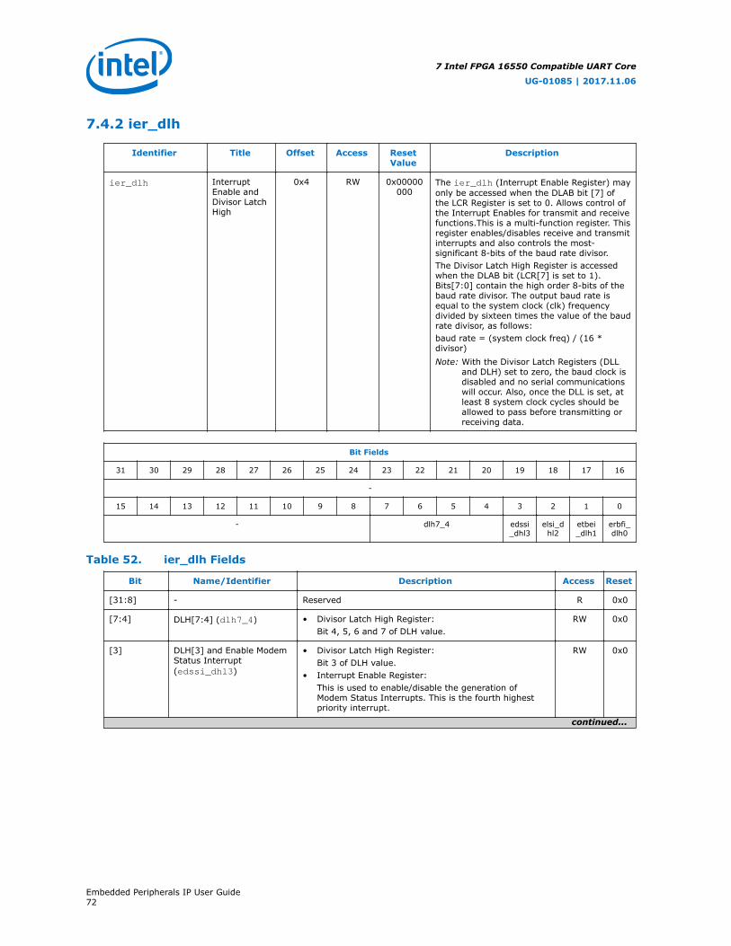
7.4.2 ier_dlh
Identifier Title Offset Access ResetValue
Description
ier_dlh InterruptEnable andDivisor LatchHigh
0x4 RW 0x00000000
The ier_dlh (Interrupt Enable Register) mayonly be accessed when the DLAB bit [7] ofthe LCR Register is set to 0. Allows control ofthe Interrupt Enables for transmit and receivefunctions.This is a multi-function register. Thisregister enables/disables receive and transmitinterrupts and also controls the most-significant 8-bits of the baud rate divisor.The Divisor Latch High Register is accessedwhen the DLAB bit (LCR[7] is set to 1).Bits[7:0] contain the high order 8-bits of thebaud rate divisor. The output baud rate isequal to the system clock (clk) frequencydivided by sixteen times the value of the baudrate divisor, as follows:baud rate = (system clock freq) / (16 *divisor)Note: With the Divisor Latch Registers (DLL
and DLH) set to zero, the baud clock isdisabled and no serial communicationswill occur. Also, once the DLL is set, atleast 8 system clock cycles should beallowed to pass before transmitting orreceiving data.
Bit Fields
31 30 29 28 27 26 25 24 23 22 21 20 19 18 17 16
-
15 14 13 12 11 10 9 8 7 6 5 4 3 2 1 0
- dlh7_4 edssi_dhl3
elsi_dhl2
etbei_dlh1
erbfi_dlh0
Table 52. ier_dlh Fields
Bit Name/Identifier Description Access Reset
[31:8] - Reserved R 0x0
[7:4] DLH[7:4] (dlh7_4) • Divisor Latch High Register:Bit 4, 5, 6 and 7 of DLH value.
RW 0x0
[3] DLH[3] and Enable ModemStatus Interrupt(edssi_dhl3)
• Divisor Latch High Register:Bit 3 of DLH value.
• Interrupt Enable Register:This is used to enable/disable the generation ofModem Status Interrupts. This is the fourth highestpriority interrupt.
RW 0x0
continued...
7 Intel FPGA 16550 Compatible UART Core
UG-01085 | 2017.11.06
Embedded Peripherals IP User Guide72

Bit Name/Identifier Description Access Reset
[2] DLH[2] and Enable ReceiverLine Status (elsi_dhl2)
• Divisor Latch High Register:Bit 2 of DLH value.
• Interrupt Enable Register:This is used to enable/disable the generation ofReceiver Line Status Interrupt. This is the highestpriority interrupt
RW 0x0
[1] DLH[1] and Transmit DataInterrupt Control(etbei_dlh1)
• Divisor Latch High Register:Bit 1 of DLH value.
• Interrupt Enable Register:Enable Transmit Holding Register Empty Interrupt. Thisis used to enable/disable the generation of TransmitterHolding Register Empty Interrupt. This is the thirdhighest priority interrupt.
RW 0x0
[0] DLH[0] and Receive DataInterrupt Enable(erbfi_dlh0)
• Divisor Latch High Register:Bit 0 of DLH value.
• Interrupt Enable Register:This is used to enable/disable the generation of theReceive Data Available Interrupt and the CharacterTimeout Interrupt (if FIFO's enabled). These are thesecond highest priority interrupts.
RW 0x0
7 Intel FPGA 16550 Compatible UART Core
UG-01085 | 2017.11.06
Embedded Peripherals IP User Guide73
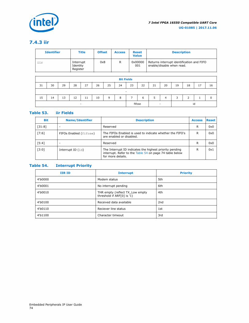
7.4.3 iir
Identifier Title Offset Access ResetValue
Description
iir InterruptIdentityRegister
0x8 R 0x00000001
Returns interrupt identification and FIFOenable/disable when read.
Bit Fields
31 30 29 28 27 26 25 24 23 22 21 20 19 18 17 16
-
15 14 13 12 11 10 9 8 7 6 5 4 3 2 1 0
- fifose - id
Table 53. iir Fields
Bit Name/Identifier Description Access Reset
[31:8] - Reserved R 0x0
[7:6] FIFOs Enabled (fifose) The FIFOs Enabled is used to indicate whether the FIFO'sare enabled or disabled.
R 0x0
[5:4] - Reserved R 0x0
[3:0] Interrupt ID (id) The Interrupt ID indicates the highest priority pendinginterrupt. Refer to the Table 54 on page 74 table belowfor more details.
R 0x1
Table 54. Interrupt Priority
IIR ID Interrupt Priority
4'b0000 Modem status 5th
4'b0001 No interrupt pending 6th
4'b0010 THR empty (reflect TX_Low emptythreshold if ARF[0] is '1)
4th
4'b0100 Received data available 2nd
4'b0110 Reciever line status 1st
4'b1100 Character timeout 3rd
7 Intel FPGA 16550 Compatible UART Core
UG-01085 | 2017.11.06
Embedded Peripherals IP User Guide74
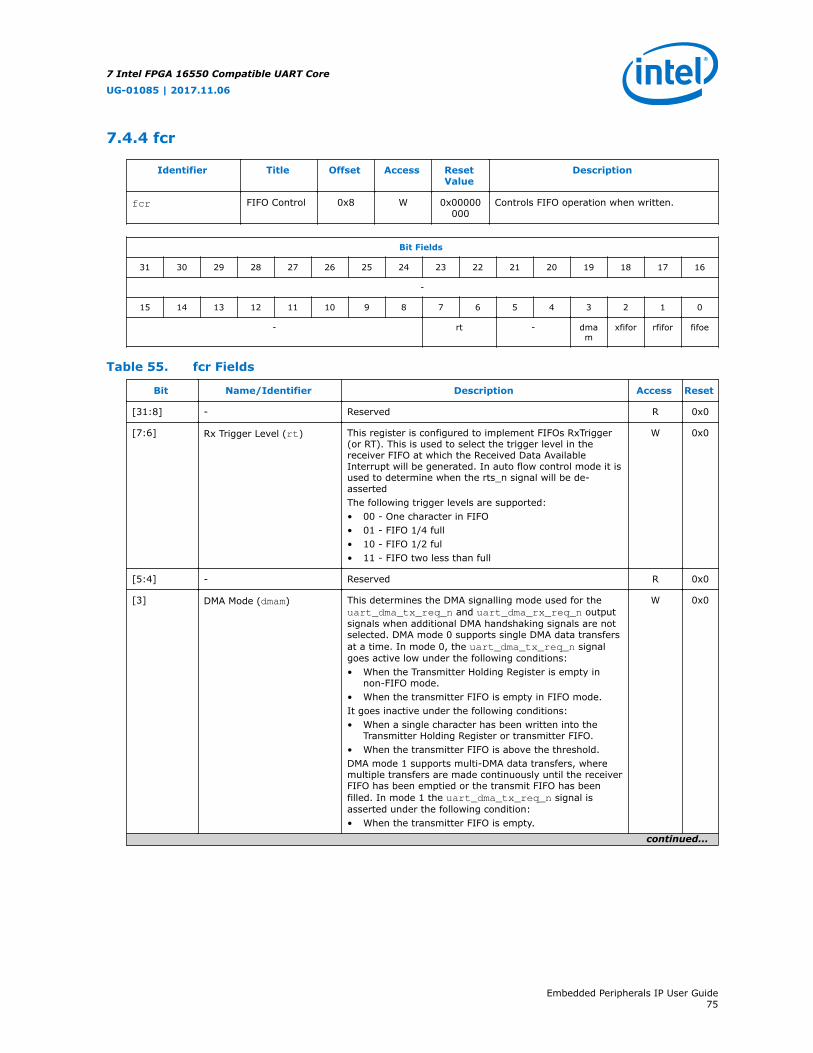
7.4.4 fcr
Identifier Title Offset Access ResetValue
Description
fcr FIFO Control 0x8 W 0x00000000
Controls FIFO operation when written.
Bit Fields
31 30 29 28 27 26 25 24 23 22 21 20 19 18 17 16
-
15 14 13 12 11 10 9 8 7 6 5 4 3 2 1 0
- rt - dmam
xfifor rfifor fifoe
Table 55. fcr Fields
Bit Name/Identifier Description Access Reset
[31:8] - Reserved R 0x0
[7:6] Rx Trigger Level (rt) This register is configured to implement FIFOs RxTrigger(or RT). This is used to select the trigger level in thereceiver FIFO at which the Received Data AvailableInterrupt will be generated. In auto flow control mode it isused to determine when the rts_n signal will be de-assertedThe following trigger levels are supported:• 00 - One character in FIFO• 01 - FIFO 1/4 full• 10 - FIFO 1/2 ful• 11 - FIFO two less than full
W 0x0
[5:4] - Reserved R 0x0
[3] DMA Mode (dmam) This determines the DMA signalling mode used for theuart_dma_tx_req_n and uart_dma_rx_req_n outputsignals when additional DMA handshaking signals are notselected. DMA mode 0 supports single DMA data transfersat a time. In mode 0, the uart_dma_tx_req_n signalgoes active low under the following conditions:• When the Transmitter Holding Register is empty in
non-FIFO mode.• When the transmitter FIFO is empty in FIFO mode.It goes inactive under the following conditions:• When a single character has been written into the
Transmitter Holding Register or transmitter FIFO.• When the transmitter FIFO is above the threshold.DMA mode 1 supports multi-DMA data transfers, wheremultiple transfers are made continuously until the receiverFIFO has been emptied or the transmit FIFO has beenfilled. In mode 1 the uart_dma_tx_req_n signal isasserted under the following condition:• When the transmitter FIFO is empty.
W 0x0
continued...
7 Intel FPGA 16550 Compatible UART Core
UG-01085 | 2017.11.06
Embedded Peripherals IP User Guide75

Bit Name/Identifier Description Access Reset
[2] Tx FIFO Reset (xfifor) This bit resets the control portion of the transmit FIFO andtreats the FIFO as empty. Note that this bit is 'self-clearing' and it is not necessary to clear this bit. Pleaseallow for 8 clock cycles to pass after changing this registerbit before reading from RBR or writing to THR.
W 0x0
[1] Rx FIFO Reset (rfifor) Resets the control portion of the receive FIFO and treatsthe FIFO as empty. Note that this bit is self-clearing' and itis not necessary to clear this bit. Allow for 8 clock cyclesto pass after changing this register bit before readingfrom RBR or writing to THR.
W 0x0
[0] FIFO Enable (fifoe) This bit enables/disables the transmit (Tx) and receive(Rx ) FIFO's. Whenever the value of this bit is changedboth the Tx and Rx controller portion of FIFO's will bereset.Any existing data in both Tx and Rx FIFO will be lost whenthis bit is changed. Please allow for 8 clock cycles to passafter changing this register bit before reading from RBR orwriting to THR.
W 0x0
7 Intel FPGA 16550 Compatible UART Core
UG-01085 | 2017.11.06
Embedded Peripherals IP User Guide76
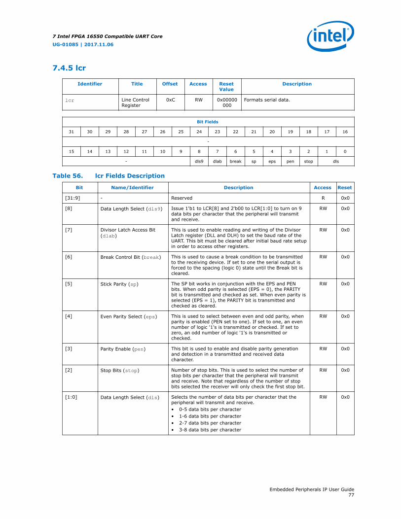
7.4.5 lcr
Identifier Title Offset Access ResetValue
Description
lcr Line ControlRegister
0xC RW 0x00000000
Formats serial data.
Bit Fields
31 30 29 28 27 26 25 24 23 22 21 20 19 18 17 16
-
15 14 13 12 11 10 9 8 7 6 5 4 3 2 1 0
- dls9 dlab break sp eps pen stop dls
Table 56. lcr Fields Description
Bit Name/Identifier Description Access Reset
[31:9] - Reserved R 0x0
[8] Data Length Select (dls9) Issue 1'b1 to LCR[8] and 2'b00 to LCR[1:0] to turn on 9data bits per character that the peripheral will transmitand receive.
RW 0x0
[7] Divisor Latch Access Bit(dlab)
This is used to enable reading and writing of the DivisorLatch register (DLL and DLH) to set the baud rate of theUART. This bit must be cleared after initial baud rate setupin order to access other registers.
RW 0x0
[6] Break Control Bit (break) This is used to cause a break condition to be transmittedto the receiving device. If set to one the serial output isforced to the spacing (logic 0) state until the Break bit iscleared.
RW 0x0
[5] Stick Parity (sp) The SP bit works in conjunction with the EPS and PENbits. When odd parity is selected (EPS = 0), the PARITYbit is transmitted and checked as set. When even parity isselected (EPS = 1), the PARITY bit is transmitted andchecked as cleared.
RW 0x0
[4] Even Parity Select (eps) This is used to select between even and odd parity, whenparity is enabled (PEN set to one). If set to one, an evennumber of logic '1's is transmitted or checked. If set tozero, an odd number of logic '1's is transmitted orchecked.
RW 0x0
[3] Parity Enable (pen) This bit is used to enable and disable parity generationand detection in a transmitted and received datacharacter.
RW 0x0
[2] Stop Bits (stop) Number of stop bits. This is used to select the number ofstop bits per character that the peripheral will transmitand receive. Note that regardless of the number of stopbits selected the receiver will only check the first stop bit.
RW 0x0
[1:0] Data Length Select (dls) Selects the number of data bits per character that theperipheral will transmit and receive.• 0-5 data bits per character• 1-6 data bits per character• 2-7 data bits per character• 3-8 data bits per character
RW 0x0
7 Intel FPGA 16550 Compatible UART Core
UG-01085 | 2017.11.06
Embedded Peripherals IP User Guide77
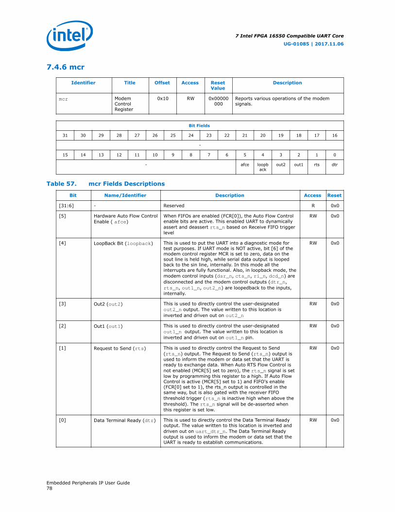
7.4.6 mcr
Identifier Title Offset Access ResetValue
Description
mcr ModemControlRegister
0x10 RW 0x00000000
Reports various operations of the modemsignals.
Bit Fields
31 30 29 28 27 26 25 24 23 22 21 20 19 18 17 16
-
15 14 13 12 11 10 9 8 7 6 5 4 3 2 1 0
- afce loopback
out2 out1 rts dtr
Table 57. mcr Fields Descriptions
Bit Name/Identifier Description Access Reset
[31:6] - Reserved R 0x0
[5] Hardware Auto Flow ControlEnable ( afce)
When FIFOs are enabled (FCR[0]), the Auto Flow Controlenable bits are active. This enabled UART to dynamicallyassert and deassert rts_n based on Receive FIFO triggerlevel
RW 0x0
[4] LoopBack Bit (loopback) This is used to put the UART into a diagnostic mode fortest purposes. If UART mode is NOT active, bit [6] of themodem control register MCR is set to zero, data on thesout line is held high, while serial data output is loopedback to the sin line, internally. In this mode all theinterrupts are fully functional. Also, in loopback mode, themodem control inputs (dsr_n, cts_n, ri_n, dcd_n) aredisconnected and the modem control outputs (dtr_n,rts_n, out1_n, out2_n) are loopedback to the inputs,internally.
RW 0x0
[3] Out2 (out2) This is used to directly control the user-designatedout2_n output. The value written to this location isinverted and driven out on out2_n
RW 0x0
[2] Out1 (out1) This is used to directly control the user-designatedout1_n output. The value written to this location isinverted and driven out on out1_n pin.
RW 0x0
[1] Request to Send (rts) This is used to directly control the Request to Send(rts_n) output. The Request to Send (rts_n) output isused to inform the modem or data set that the UART isready to exchange data. When Auto RTS Flow Control isnot enabled (MCR[5] set to zero), the rts_n signal is setlow by programming this register to a high. If Auto FlowControl is active (MCR[5] set to 1) and FIFO's enable(FCR[0] set to 1), the rts_n output is controlled in thesame way, but is also gated with the receiver FIFOthreshold trigger (rts_n is inactive high when above thethreshold). The rts_n signal will be de-asserted whenthis register is set low.
RW 0x0
[0] Data Terminal Ready (dtr) This is used to directly control the Data Terminal Readyoutput. The value written to this location is inverted anddriven out on uart_dtr_n. The Data Terminal Readyoutput is used to inform the modem or data set that theUART is ready to establish communications.
RW 0x0
7 Intel FPGA 16550 Compatible UART Core
UG-01085 | 2017.11.06
Embedded Peripherals IP User Guide78
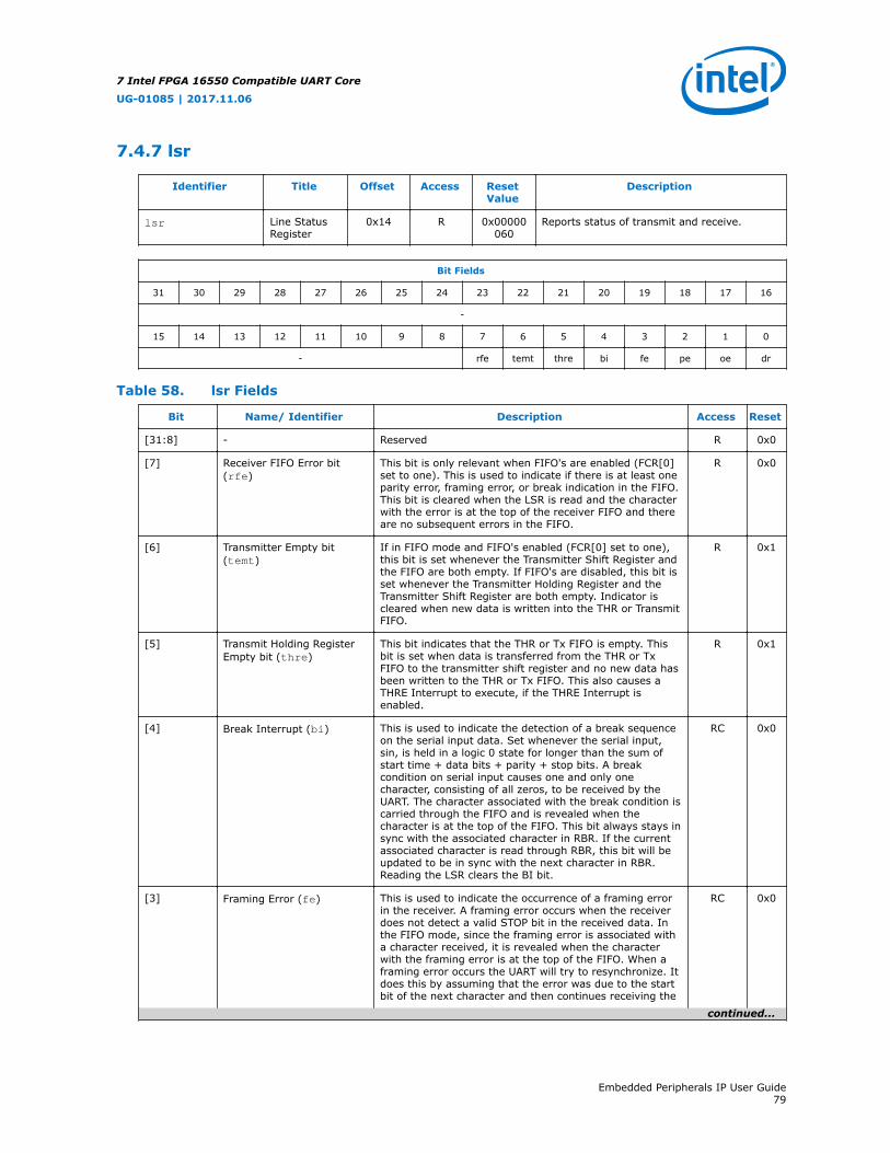
7.4.7 lsr
Identifier Title Offset Access ResetValue
Description
lsr Line StatusRegister
0x14 R 0x00000060
Reports status of transmit and receive.
Bit Fields
31 30 29 28 27 26 25 24 23 22 21 20 19 18 17 16
-
15 14 13 12 11 10 9 8 7 6 5 4 3 2 1 0
- rfe temt thre bi fe pe oe dr
Table 58. lsr Fields
Bit Name/ Identifier Description Access Reset
[31:8] - Reserved R 0x0
[7] Receiver FIFO Error bit(rfe)
This bit is only relevant when FIFO's are enabled (FCR[0]set to one). This is used to indicate if there is at least oneparity error, framing error, or break indication in the FIFO.This bit is cleared when the LSR is read and the characterwith the error is at the top of the receiver FIFO and thereare no subsequent errors in the FIFO.
R 0x0
[6] Transmitter Empty bit(temt)
If in FIFO mode and FIFO's enabled (FCR[0] set to one),this bit is set whenever the Transmitter Shift Register andthe FIFO are both empty. If FIFO's are disabled, this bit isset whenever the Transmitter Holding Register and theTransmitter Shift Register are both empty. Indicator iscleared when new data is written into the THR or TransmitFIFO.
R 0x1
[5] Transmit Holding RegisterEmpty bit (thre)
This bit indicates that the THR or Tx FIFO is empty. Thisbit is set when data is transferred from the THR or TxFIFO to the transmitter shift register and no new data hasbeen written to the THR or Tx FIFO. This also causes aTHRE Interrupt to execute, if the THRE Interrupt isenabled.
R 0x1
[4] Break Interrupt (bi) This is used to indicate the detection of a break sequenceon the serial input data. Set whenever the serial input,sin, is held in a logic 0 state for longer than the sum ofstart time + data bits + parity + stop bits. A breakcondition on serial input causes one and only onecharacter, consisting of all zeros, to be received by theUART. The character associated with the break condition iscarried through the FIFO and is revealed when thecharacter is at the top of the FIFO. This bit always stays insync with the associated character in RBR. If the currentassociated character is read through RBR, this bit will beupdated to be in sync with the next character in RBR.Reading the LSR clears the BI bit.
RC 0x0
[3] Framing Error (fe) This is used to indicate the occurrence of a framing errorin the receiver. A framing error occurs when the receiverdoes not detect a valid STOP bit in the received data. Inthe FIFO mode, since the framing error is associated witha character received, it is revealed when the characterwith the framing error is at the top of the FIFO. When aframing error occurs the UART will try to resynchronize. Itdoes this by assuming that the error was due to the startbit of the next character and then continues receiving the
RC 0x0
continued...
7 Intel FPGA 16550 Compatible UART Core
UG-01085 | 2017.11.06
Embedded Peripherals IP User Guide79
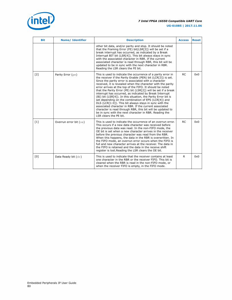
Bit Name/ Identifier Description Access Reset
other bit data, and/or parity and stop. It should be notedthat the Framing Error (FE) bit(LSR[3]) will be set if abreak interrupt has occurred, as indicated by a BreakInterrupt BIT bit (LSR[4]). This bit always stays in syncwith the associated character in RBR. If the currentassociated character is read through RBR, this bit will beupdated to be in sync with the next character in RBR.Reading the LSR clears the FE bit.
[2] Parity Error (pe) This is used to indicate the occurrence of a parity error inthe receiver if the Parity Enable (PEN) bit (LCR[3]) is set.Since the parity error is associated with a characterreceived, it is revealed when the character with the parityerror arrives at the top of the FIFO. It should be notedthat the Parity Error (PE) bit (LSR[2]) will be set if a breakinterrupt has occurred, as indicated by Break Interrupt(BI) bit (LSR[4]). In this situation, the Parity Error bit isset depending on the combination of EPS (LCR[4]) andDLS (LCR[1:0]). This bit always stays in sync with theassociated character in RBR. If the current associatedcharacter is read through RBR, this bit will be updated tobe in sync with the next character in RBR. Reading theLSR clears the PE bit.
RC 0x0
[1] Overrun error bit (oe) This is used to indicate the occurrence of an overrun error.This occurs if a new data character was received beforethe previous data was read. In the non-FIFO mode, theOE bit is set when a new character arrives in the receiverbefore the previous character was read from the RBR.When this happens, the data in the RBR is overwritten. Inthe FIFO mode, an overrun error occurs when the FIFO isfull and new character arrives at the receiver. The data inthe FIFO is retained and the data in the receive shiftregister is lost.Reading the LSR clears the OE bit.
RC 0x0
[0] Data Ready bit (dr) This is used to indicate that the receiver contains at leastone character in the RBR or the receiver FIFO. This bit iscleared when the RBR is read in the non-FIFO mode, orwhen the receiver FIFO is empty, in the FIFO mode.
R 0x0
7 Intel FPGA 16550 Compatible UART Core
UG-01085 | 2017.11.06
Embedded Peripherals IP User Guide80

7.4.8 msr
Identifier Title Offset Access ResetValue
Description
msr ModemStatusRegister
0x18 R 0x00000000
It should be noted that whenever bits 0, 1, 2or 3 are set to logic one, to indicate a changeon the modem control inputs, a modemstatus interrupt will be generated if enabledvia the IER regardless of when the changeoccurred. Since the delta bits (bits 0, 1, 3)can get set after a reset if their respectivemodem signals are active (see individual bitsfor details), a read of the MSR after reset canbe performed to prevent unwanted interrupts.
Bit Fields
31 30 29 28 27 26 25 24 23 22 21 20 19 18 17 16
-
15 14 13 12 11 10 9 8 7 6 5 4 3 2 1 0
- dcd ri dsr cts ddcd teri ddsr dcts
Table 59. msr Fields
Bit Name/Identifier Description Access Reset
[31:8] - Reserved R 0x0
[7] Data Carrier Detect(dcd)
This bit is the complement of the modem controlline (dcd_n). This bit is used to indicate thecurrent state of dcd_n. When the Data CarrierDetect input (dcd_n) is asserted it is an indicationthat the carrier has been detected by the modemor data set.
R 0x0
[6] Ring Indicator (ri) This bit is the complement of modem control line(ri_n). This bit is used to indicate the currentstate of ri_n. When the Ring Indicator input(ri_n) is asserted it is an indication that atelephone ringing signal has been received by themodem or data set.
R 0x0
[5] Data Set Ready (dsr) This bit is the complement of modem control linedsr_n. This bit is used to indicate the currentstate of dsr_n. When the Data Set Ready input(dsr_n) is asserted it is an indication that themodem or data set is ready to establishcommunications with the uart.
R 0x0
[4] Clear to Send (cts) This bit is the complement of modem control linects_n. This bit is used to indicate the currentstate of cts_n. When the Clear to Send input(cts_n) is asserted it is an indication that themodem or data set is ready to exchange data withthe uart.
R 0x0
[3] Delta Data CarrierDetect (ddcd)
This is used to indicate that the modem controlline dcd_n has changed since the last time theMSR was read. Reading the MSR clears the DDCDbit.
RC 0x0
continued...
7 Intel FPGA 16550 Compatible UART Core
UG-01085 | 2017.11.06
Embedded Peripherals IP User Guide81

Bit Name/Identifier Description Access Reset
Note: If the DDCD bit is not set and the dcd_nsignal is asserted (low) and a reset occurs(software or otherwise), then the DDCD bitwill get set when the reset is removed ifthe dcd_n signal remains asserted.
[2] Trailing Edge of RingIndicator (teri)
This is used to indicate that a change on the inputri_n (from an active low, to an inactive highstate) has occurred since the last time the MSRwas read. Reading the MSR clears the TERI bit.
RC 0x0
[1] Delta Data Set Ready(ddsr)
This is used to indicate that the modem controlline dsr_n has changed since the last time theMSR was read. Reading the MSR clears the DDSRbit.Note: If the DDSR bit is not set and the dsr_n
signal is asserted (low) and a reset occurs(software or otherwise), then the DDSR bitwill get set when the reset is removed ifthe dsr_n signal remains asserted.
RC 0x0
[0] Delta Clear to Send(dcts)
This is used to indicate that the modem controlline cts_n has changed since the last time theMSR was read. Reading the MSR clears the DCTSbit.Note: If the DCTS bit is not set and the cts_n
signal is asserted (low) and a reset occurs(software or otherwise), then the DCTS bitwill get set when the reset is removed ifthe cts_n signal remains asserted.
RC 0x0
7 Intel FPGA 16550 Compatible UART Core
UG-01085 | 2017.11.06
Embedded Peripherals IP User Guide82
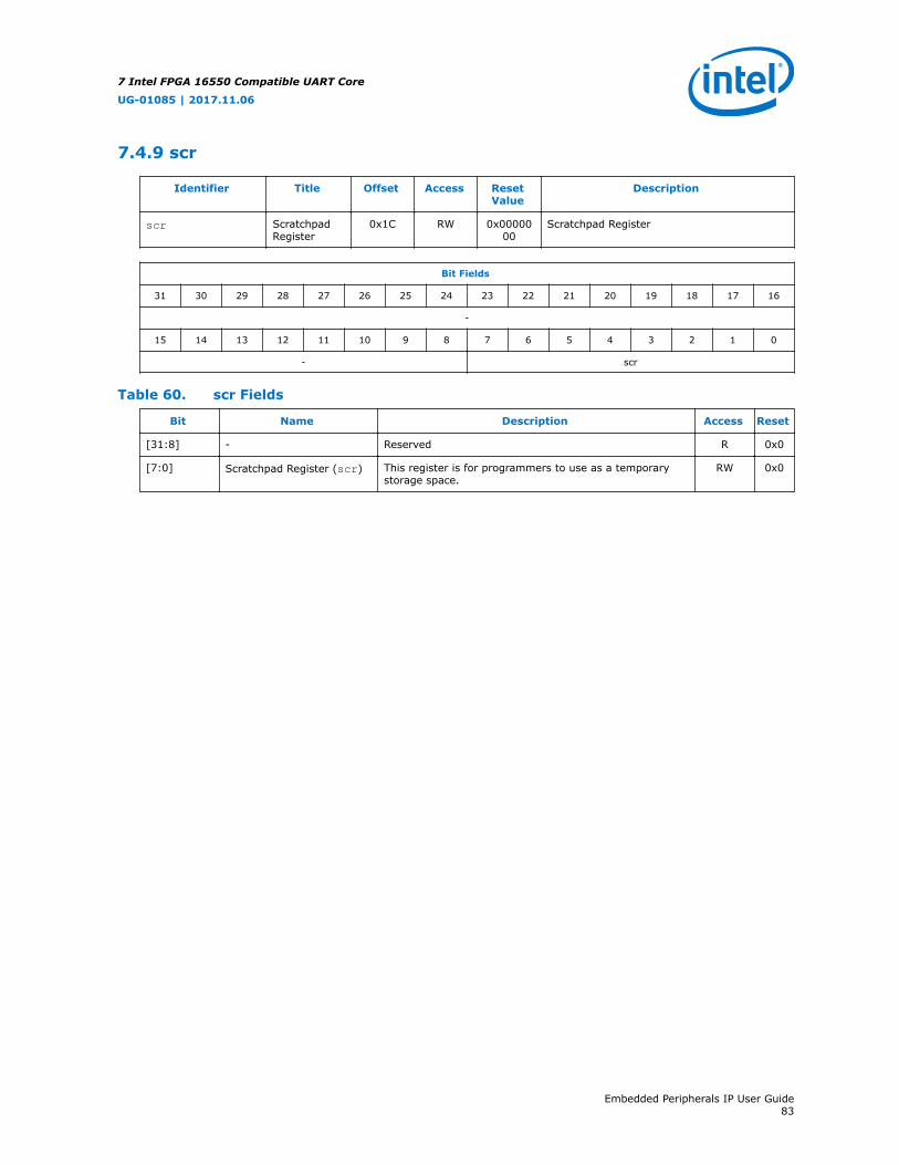
7.4.9 scr
Identifier Title Offset Access ResetValue
Description
scr ScratchpadRegister
0x1C RW 0x0000000
Scratchpad Register
Bit Fields
31 30 29 28 27 26 25 24 23 22 21 20 19 18 17 16
-
15 14 13 12 11 10 9 8 7 6 5 4 3 2 1 0
- scr
Table 60. scr Fields
Bit Name Description Access Reset
[31:8] - Reserved R 0x0
[7:0] Scratchpad Register (scr) This register is for programmers to use as a temporarystorage space.
RW 0x0
7 Intel FPGA 16550 Compatible UART Core
UG-01085 | 2017.11.06
Embedded Peripherals IP User Guide83
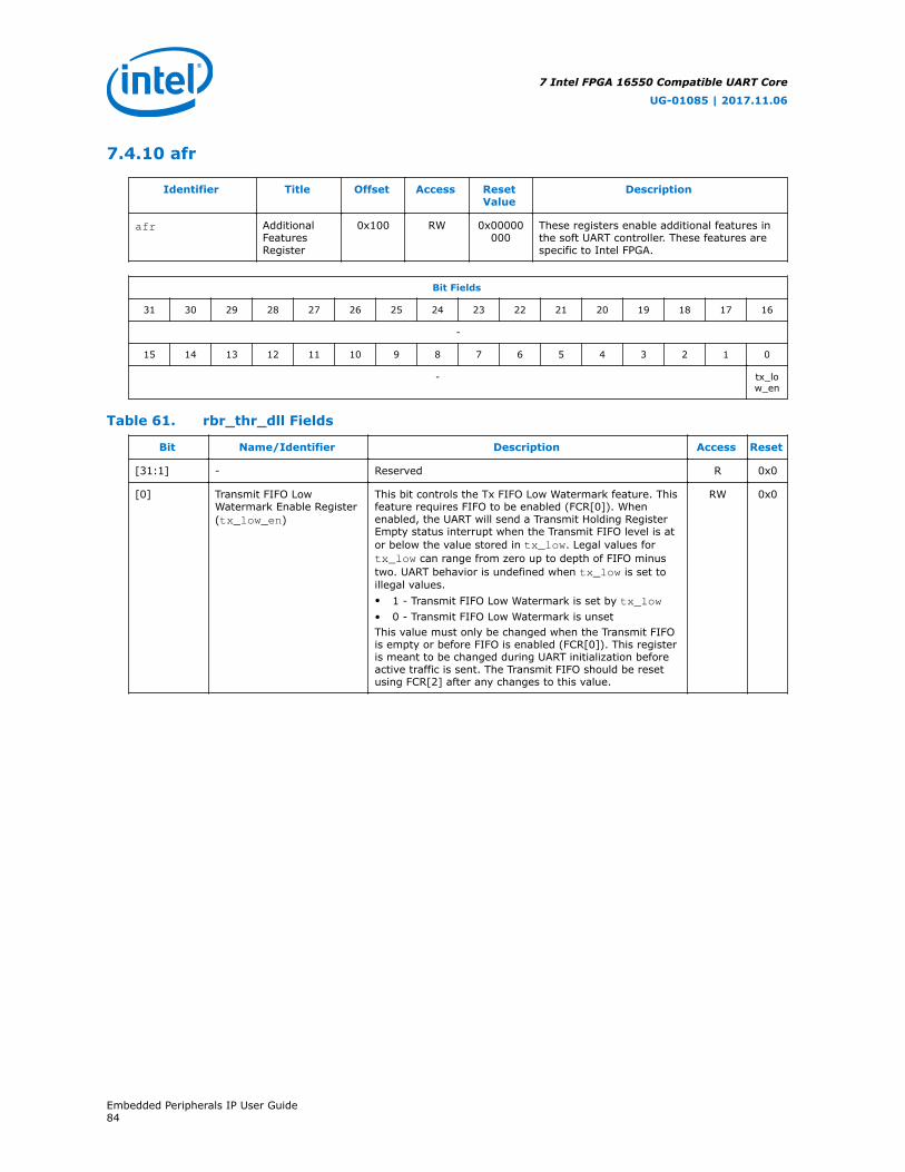
7.4.10 afr
Identifier Title Offset Access ResetValue
Description
afr AdditionalFeaturesRegister
0x100 RW 0x00000000
These registers enable additional features inthe soft UART controller. These features arespecific to Intel FPGA.
Bit Fields
31 30 29 28 27 26 25 24 23 22 21 20 19 18 17 16
-
15 14 13 12 11 10 9 8 7 6 5 4 3 2 1 0
- tx_low_en
Table 61. rbr_thr_dll Fields
Bit Name/Identifier Description Access Reset
[31:1] - Reserved R 0x0
[0] Transmit FIFO LowWatermark Enable Register(tx_low_en)
This bit controls the Tx FIFO Low Watermark feature. Thisfeature requires FIFO to be enabled (FCR[0]). Whenenabled, the UART will send a Transmit Holding RegisterEmpty status interrupt when the Transmit FIFO level is ator below the value stored in tx_low. Legal values fortx_low can range from zero up to depth of FIFO minustwo. UART behavior is undefined when tx_low is set toillegal values.• 1 - Transmit FIFO Low Watermark is set by tx_low• 0 - Transmit FIFO Low Watermark is unsetThis value must only be changed when the Transmit FIFOis empty or before FIFO is enabled (FCR[0]). This registeris meant to be changed during UART initialization beforeactive traffic is sent. The Transmit FIFO should be resetusing FCR[2] after any changes to this value.
RW 0x0
7 Intel FPGA 16550 Compatible UART Core
UG-01085 | 2017.11.06
Embedded Peripherals IP User Guide84

7.4.11 tx_low
Identifier Title Offset Access ResetValue
Description
tx_low TransmitFIFO LowWatermarkRegister
ox104 RW 0x00000000
This register is used to set the value of theTransmit FIFO Low Watermark.
Bit Fields
31 30 29 28 27 26 25 24 23 22 21 20 19 18 17 16
-
15 14 13 12 11 10 9 8 7 6 5 4 3 2 1 0
- value
Table 62. rbr_thr_dll Fields
Bit Name/Identifier Description Access Reset
[31:9] - Reserved R 0x0
[8:0] Transmit FIFO LowWatermark (value)
Set the Transmit FIFO Low Watermark Value.The lowest legal value is zeroThe highest legal value is two less than the FIFO DepthThis value must only be changed when the Transmit FIFOis empty or before FIFO is enabled (FCR[0]).
RW 0x00
7.5 Document Revision History
Table 63. 16550 UART Core Revision History
Date Version Changes
November 2017 2017.11.06 Removed the minimum clock requirement in the Table: Clock and ResetSignal Interface.
October 2016 2016.10.28 Two new registers:• afr on page 84• tx_low on page 85Updated:• lsr on page 79 Bit [5]• fcr on page 75 Bit [7:6]• New table added to iir on page 74 section
December 2015 2015.12.16 Product ID changed in "16550 UART Release Information" section.
November 2015 2015.11.06 Updated the following topics:• Core Overview on page 51• Feature Description
— Table 30 on page 51• General Architecture
— Figure 17 on page 54• Configuration Parameters
— Table 37 on page 56• DMA Support on page 56
continued...
7 Intel FPGA 16550 Compatible UART Core
UG-01085 | 2017.11.06
Embedded Peripherals IP User Guide85
Date Version Changes
• Supported Features— Table 41 on page 61
• Configuration— Figure 24 on page 62
• UART Device Structure on page 64— Example 1 and 2
• Address Map and Register Descriptions on page 70
June 2015 2015.06.12 • Added "16550 UART General Programming Flow Chart" section• Added "16550 UART Release Information" section• Added "Address Map and Register Descriptions" section• Added Stick parity/Force parity feature into the "UART Features and
Configurability" table in the "Feature Description" section• Updated "Interface" section with sout_oe signal details in the "Flow
Control" table• Updated "Underrun" section
July 2014 2014.07.24 Initial Release.
7 Intel FPGA 16550 Compatible UART Core
UG-01085 | 2017.11.06
Embedded Peripherals IP User Guide86
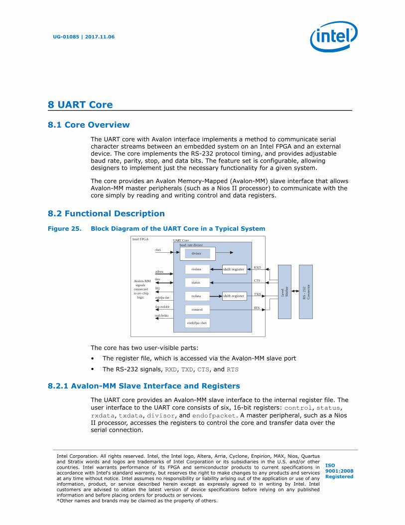
8 UART Core
8.1 Core Overview
The UART core with Avalon interface implements a method to communicate serialcharacter streams between an embedded system on an Intel FPGA and an externaldevice. The core implements the RS-232 protocol timing, and provides adjustablebaud rate, parity, stop, and data bits. The feature set is configurable, allowingdesigners to implement just the necessary functionality for a given system.
The core provides an Avalon Memory-Mapped (Avalon-MM) slave interface that allowsAvalon-MM master peripherals (such as a Nios II processor) to communicate with thecore simply by reading and writing control and data registers.
8.2 Functional Description
Figure 25. Block Diagram of the UART Core in a Typical System
UART Corebaud rate divisor
shift register RXD
RTS
CTS
TXD Leve
l S
hift
er
RS
- 2
32C
onne
ctor
Avalon-MM signalsconnectedto on- chip logic
data
IRQ
data available
ready fordata
endofpa cket
address
clock
rxdata
status
control
txdata
endofpa cket
shift register
divisor
Intel FPGA
The core has two user-visible parts:
• The register file, which is accessed via the Avalon-MM slave port
• The RS-232 signals, RXD, TXD, CTS, and RTS
8.2.1 Avalon-MM Slave Interface and Registers
The UART core provides an Avalon-MM slave interface to the internal register file. Theuser interface to the UART core consists of six, 16-bit registers: control, status,rxdata, txdata, divisor, and endofpacket. A master peripheral, such as a NiosII processor, accesses the registers to control the core and transfer data over theserial connection.
UG-01085 | 2017.11.06
Intel Corporation. All rights reserved. Intel, the Intel logo, Altera, Arria, Cyclone, Enpirion, MAX, Nios, Quartusand Stratix words and logos are trademarks of Intel Corporation or its subsidiaries in the U.S. and/or othercountries. Intel warrants performance of its FPGA and semiconductor products to current specifications inaccordance with Intel's standard warranty, but reserves the right to make changes to any products and servicesat any time without notice. Intel assumes no responsibility or liability arising out of the application or use of anyinformation, product, or service described herein except as expressly agreed to in writing by Intel. Intelcustomers are advised to obtain the latest version of device specifications before relying on any publishedinformation and before placing orders for products or services.*Other names and brands may be claimed as the property of others.
ISO9001:2008Registered
The UART core provides an active-high interrupt request (IRQ) output that can requestan interrupt when new data has been received, or when the core is ready to transmitanother character. For further details, refer to the Interrupt Behavior section.
For more information, refer to Interval Timer Core section.
For details about the Avalon-MM interface, refer to the Avalon Interface Specifications.
8.2.2 RS-232 Interface
The UART core implements RS-232 asynchronous transmit and receive logic. TheUART core sends and receives serial data via the TXD and RXD ports. The I/O bufferson most Intel FPGA families do not comply with RS-232 voltage levels, and may bedamaged if driven directly by signals from an RS-232 connector. To comply withRS-232 voltage signaling specifications, an external level-shifting buffer is required(for example, Maxim MAX3237) between the FPGA I/O pins and the external RS-232connector.
The UART core uses a logic 0 for mark, and a logic 1 for space. An inverter inside theFPGA can be used to reverse the polarity of any of the RS-232 signals, if necessary.
8.2.3 Transmitter Logic
The UART transmitter consists of a 7-, 8-, or 9-bit txdata holding register and acorresponding 7-, 8-, or 9-bit transmit shift register. Avalon-MM master peripheralswrite the txdata holding register via the Avalon-MM slave port. The transmit shiftregister is loaded from the txdata register automatically when a serial transmit shiftoperation is not currently in progress. The transmit shift register directly feeds theTXD output. Data is shifted out to TXD LSB first.
These two registers provide double buffering. A master peripheral can write a newvalue into the txdata register while the previously written character is being shiftedout. The master peripheral can monitor the transmitter's status by reading thestatus register's transmitter ready (TRDY), transmitter shift register empty (tmt),and transmitter overrun error (TOE) bits.
The transmitter logic automatically inserts the correct number of start, stop, andparity bits in the serial TXD data stream as required by the RS-232 specification.
8.2.4 Receiver Logic
The UART receiver consists of a 7-, 8-, or 9-bit receiver-shift register and acorresponding 7-, 8-, or 9-bit rxdata holding register. Avalon-MM master peripheralsread the rxdata holding register via the Avalon-MM slave port. The rxdata holdingregister is loaded from the receiver shift register automatically every time a newcharacter is fully received.
These two registers provide double buffering. The rxdata register can hold apreviously received character while the subsequent character is being shifted into thereceiver shift register.
A master peripheral can monitor the receiver's status by reading the statusregister's read-ready (RRDY), receiver-overrun error (ROE), break detect (BRK), parityerror (PE), and framing error (FE) bits. The receiver logic automatically detects the
8 UART Core
UG-01085 | 2017.11.06
Embedded Peripherals IP User Guide88
correct number of start, stop, and parity bits in the serial RXD stream as required bythe RS-232 specification. The receiver logic checks for four exceptional conditions,frame error, parity error, receive overrun error, and break, in the received data andsets corresponding status register bits.
8.2.5 Baud Rate Generation
The UART core's internal baud clock is derived from the Avalon-MM clock input. Theinternal baud clock is generated by a clock divider. The divisor value can come fromone of the following sources:
• A constant value specified at system generation time
• The 16-bit value stored in the divisor register
The divisor register is an optional hardware feature. If it is disabled at systemgeneration time, the divisor value is fixed and the baud rate cannot be altered.
8.3 Instantiating the Core
Instantiating the UART in hardware creates at least two I/O ports for each UART core:An RXD input, and a TXD output. The following sections describe the available options.
8.3.1 Configuration Settings
This section describes the configuration settings.
8.3.1.1 Baud Rate Options
The UART core can implement any of the standard baud rates for RS-232 connections.The baud rate can be configured in one of two ways:
• Fixed rate—The baud rate is fixed at system generation time and cannot bechanged via the Avalon-MM slave port.
• Variable rate—The baud rate can vary, based on a clock divisor value held in thedivisor register. A master peripheral changes the baud rate by writing newvalues to the divisor register.
The baud rate is calculated based on the clock frequency provided by the Avalon-MM interface. Changing the system clock frequency in hardware withoutregenerating the UART core hardware results in incorrect signaling.
The baud rate is calculated based on the clock frequency provided by the Avalon-MMinterface. Changing the system clock frequency in hardware without regenerating theUART core hardware results in incorrect signaling.
8.3.1.2 Baud Rate (bps) Setting
The Baud Rate setting determines the default baud rate after reset. The Baud Rateoption offers standard preset values.
8 UART Core
UG-01085 | 2017.11.06
Embedded Peripherals IP User Guide89

The baud rate value is used to calculate an appropriate clock divisor value toimplement the desired baud rate. Baud rate and divisor values are related as shown inthe follow two equations:
Divisor Formula:
divisor int clock frequencybaud rate
----------------------------------------- 0.5 +(= )
Baud rate Formula:
baud rate clock frequencydivisor 1+
-----------------------------------------=
8.3.1.3 Baud Rate Can Be Changed By Software Setting
When this setting is on, the hardware includes a 16-bit divisor register at addressoffset 4. The divisor register is writable, so the baud rate can be changed by writinga new value to this register.
When this setting is off, the UART hardware does not include a divisor register. TheUART hardware implements a constant baud divisor, and the value cannot be changedafter system generation. In this case, writing to address offset 4 has no effect, andreading from address offset 4 produces an undefined result.
8.3.1.4 Data Bits, Stop Bits, Parity
The UART core's parity, data bits and stop bits are configurable. These settings arefixed at system generation time; they cannot be altered via the register file.
Table 64. Data Bits Settings
Setting Legal Values Description
Data Bits 7, 8, 9 This setting determines the widths ofthe txdata, rxdata, andendofpacket registers.
Stop Bits 1, 2 This setting determines whether thecore transmits 1 or 2 stop bits withevery character. The core alwaysterminates a receive transaction at thefirst stop bit, and ignores allsubsequent stop bits, regardless of thissetting.
Parity None, Even, Odd This setting determines whether theUART core transmits characters withparity checking, and whether it expectsreceived characters to have paritychecking.When Parity is set to None, thetransmit logic sends data withoutincluding a parity bit, and the receivelogic presumes the incoming data does
continued...
8 UART Core
UG-01085 | 2017.11.06
Embedded Peripherals IP User Guide90
Setting Legal Values Description
not include a parity bit. The PE bit inthe status register is notimplemented; it always reads 0.When Parity is set to Odd or Even,the transmit logic computes and insertsthe required parity bit into theoutgoing TXD bitstream, and thereceive logic checks the parity bit inthe incoming RXD bitstream. If thereceiver finds data with incorrectparity, the PE bit in the statusregister is set to 1. When Parity isEven, the parity bit is 0 if thecharacter has an even number of 1bits; otherwise the parity bit is 1.Similarly, when parity is Odd, theparity bit is 0 if the character has anodd number of 1 bits.
8.3.1.5 Synchronizer Stages
The option Synchronizer Stages allows you to specify the length of synchronizationregister chains. These register chains are used when a metastable event is likely tooccur and the length specified determines the meantime before failure. The registerchain length, however, affects the latency of the core.
For more information on metastability in Intel FPGA devices, refer to UnderstandingMetastability in FPGAs.
For more information on metastability analysis and synchronization register chains,refer to the Area and Timing Optimization chapter in volume 2 of the Intel QuartusPrime Handbook.
8.3.1.6 Streaming Data (DMA) Control
The UART core can also optionally include the end-of-packet register.
8.3.1.6.1 Include End-of-Packet Register
When this setting is on, the UART core includes:
• A 7-, 8-, or 9-bit endofpacket register at address-offset 5. The data width isdetermined by the Data Bits setting.
• EOP bit in the status register.
• IEOP bit in the control register.
• endofpacket signal.
EOP detection can be used with a DMA controller, for example, to implement a UARTthat automatically writes received characters to memory until a specified character isencountered in the incoming RXD stream. The terminating (EOP) character's value isdetermined by the endofpacket register.
When the EOP register is disabled, the UART core does not include the EOP resources.Writing to the endofpacket register has no effect, and reading produces anundefined value.
8 UART Core
UG-01085 | 2017.11.06
Embedded Peripherals IP User Guide91

8.3.2 Simulation Settings
When the UART core's logic is generated, a simulation model is also created. Thesimulation model offers features to simplify and accelerate simulation of systems thatuse the UART core. Changes to the simulation settings do not affect the behavior ofthe UART core in hardware; the settings affect only functional simulation.
Note: For simulation, the UART core will not respond to data received on the rxdataregister.
For examples of how to use the following settings to simulate Nios II systems, refer to AN 351: Simulating Nios II Embedded Processor Designs.
8.3.2.1 Simulated RXD-Input Character Stream
You can enter a character stream that is simulated entering the RXD port uponsimulated system reset. The UART core's MegaWizard™ interface accepts an arbitrarycharacter string, which is later incorporated into the UART simulation model. Afterreset in reset, the string is input into the RXD port character-by-character as the coreis able to accept new data.
8.3.2.2 Prepare Interactive Windows
At system generation time, the UART core generator can create ModelSim macros thatfacilitate interaction with the UART model during simulation. You can turn on thefollowing options:
• Create ModelSim alias to open streaming output window to create aModelSim macro that opens a window to display all output from the TXD port.
• Create ModelSim alias to open interactive stimulus window to create aModelSim macro that opens a window to accept stimulus for the RXD port. Thewindow sends any characters typed in the window to the RXD port.
8.3.2.3 Simulated Transmitter Baud Rate
RS-232 transmission rates are often slower than any other process in the system, andit is seldom useful to simulate the functional model at the true baud rate. Forexample, at 115,200 bps, it typically takes thousands of clock cycles to transfer asingle character. The UART simulation model has the ability to run with a constantclock divisor of 2, allowing the simulated UART to transfer bits at half the system clockspeed, or roughly one character per 20 clock cycles. You can choose one of thefollowing options for the simulated transmitter baud rate:
• Accelerated (use divisor = 2)—TXD emits one bit per 2 clock cycles insimulation.
• Actual (use true baud divisor)—TXD transmits at the actual baud rate, asdetermined by the divisor register.
8.4 Simulation Considerations
The simulation features were created for easy simulation of Nios II processor systemswhen using the ModelSim simulator. The documentation for the processor documentsthe suggested usage of these features. Other usages may be possible, but will requireadditional user effort to create a custom simulation process.
8 UART Core
UG-01085 | 2017.11.06
Embedded Peripherals IP User Guide92
The simulation model is implemented in the UART core's top-level HDL file; thesynthesizable HDL and the simulation HDL are implemented in the same file. Thesimulation features are implemented using translate on and translate offsynthesis directives that make certain sections of HDL code visible only to thesynthesis tool.
Do not edit the simulation directives if you are using Intel FPGA recommendedsimulation procedures. If you do change the simulation directives for your customsimulation flow, be aware that Platform Designer overwrites existing files duringsystem generation. Take precaution so that your changes are not overwritten.
For details about simulating the UART core in Nios II processor systems, refer to AN 351: Simulating Nios II Processor Designs.
8.5 Software Programming Model
The following sections describe the software programming model for the UART core,including the register map and software declarations to access the hardware. For NiosII processor users, Intel provides hardware abstraction layer (HAL) system librarydrivers that enable you to access the UART core using the ANSI C standard libraryfunctions, such as printf() and getchar().
8.5.1 HAL System Library Support
The Intel-provided driver implements a HAL character-mode device driver thatintegrates into the HAL system library for Nios II systems. HAL users should accessthe UART via the familiar HAL API and the ANSI C standard library, rather thanaccessing the UART registers. ioctl() requests are defined that allow HAL users tocontrol the hardware-dependent aspects of the UART.
Note: If your program uses the HAL device driver to access the UART hardware, accessingthe device registers directly interferes with the correct behavior of the driver.
For Nios II processor users, the HAL system library API provides complete access tothe UART core's features. Nios II programs treat the UART core as a character modedevice, and send and receive data using the ANSI C standard library functions.
The driver supports the CTS/RTS control signals when they are enabled in PlatformDesigner. Refer to Driver Options: Fast Versus Small Implementations section.
The following code demonstrates the simplest possible usage, printing a message tostdout using printf(). In this example, the system contains a UART core, and theHAL system library has been configured to use this device for stdout.
Example 4. Example: Printing Characters to a UART Core as stdout
#include <stdio.h>int main (){printf("Hello world.\n");return 0;}
8 UART Core
UG-01085 | 2017.11.06
Embedded Peripherals IP User Guide93

The following code demonstrates reading characters from and sending messages to aUART device using the C standard library. In this example, the system contains aUART core named uart1 that is not necessarily configured as the stdout device. Inthis case, the program treats the device like any other node in the HAL file system.
For more information about the HAL system library, refer to the Nios II ClassicSoftware Developer's Handbook.
Example 5. Example: Sending and Receiving Characters
/* A simple program that recognizes the characters 't' and 'v' */#include <stdio.h>#include <string.h>int main (){ char* msg = "Detected the character 't'.\n"; FILE* fp; char prompt = 0; fp = fopen ("/dev/uart1", "r+"); //Open file for reading and writing if (fp) { while (prompt != 'v') { // Loop until we receive a 'v'. prompt = getc(fp); // Get a character from the UART. if (prompt == 't') { // Print a message if character is 't'. fwrite (msg, strlen (msg), 1, fp); } } fprintf(fp, "Closing the UART file.\n"); fclose (fp); } return 0;}
8.5.1.1 Driver Options: Fast vs Small Implementations
To accommodate the requirements of different types of systems, the UART driverprovides two variants: a fast version and a small version. The fast version is thedefault. Both fast and small drivers fully support the C standard library functions andthe HAL API.
The fast driver is an interrupt-driven implementation, which allows the processor toperform other tasks when the device is not ready to send or receive data. Because theUART data rate is slow compared to the processor, the fast driver can provide a largeperformance benefit for systems that could be performing other tasks in the interim.
The small driver is a polled implementation that waits for the UART hardware beforesending and receiving each character. There are two ways to enable the small footprintdriver:
• Enable the small footprint setting for the HAL system library project. This optionaffects device drivers for all devices in the system as well.
• Specify the preprocessor option -DALTERA_AVALON_UART_SMALL. You can usethis option if you want the small, polled implementation of the UART driver, but donot want to affect the drivers for other devices.
Refer to the help system in the Nios II IDE for details about how to set HAL propertiesand preprocessor options.
8 UART Core
UG-01085 | 2017.11.06
Embedded Peripherals IP User Guide94
8.5.1.2 ioct() Operations
The UART driver supports the ioctl() function to allow HAL-based programs torequest device-specific operations. The table below defines operation requests that theUART driver supports.
Table 65. UART ioctl() Operations
Request Description
TIOCEXCL Locks the device for exclusive access. Further calls to open() for this device will fail until eitherthis file descriptor is closed, or the lock is released using the TIOCNXCL ioctl request. For thisrequest to succeed there can be no other existing file descriptors for this device. The parameterarg is ignored.
TIOCNXCL Releases a previous exclusive access lock. The parameter arg is ignored.
Additional operation requests are also optionally available for the fast driver only, asshown in Optional UART ioctl() Operations for the Fast Driver Only Table. Toenable these operations in your program, you must set the preprocessor option -DALTERA_AVALON_UART_USE_IOCTL.
Table 66. Optional UART ioctl() Operations for the Fast Driver Only
Request Description
TIOCMGET Returns the current configuration of the device by filling in the contents of the input termios structure. A pointer to this structure is supplied as the value of the parameter opt.
TIOCMSET Sets the configuration of the device according to the values contained in the input termios structure. A pointer to this structure is supplied as the value of the parameter arg.
Note: The termios structure is defined by the Newlib C standard library. You can find thedefinition in the file <Nios II EDS install path>/components/altera_hal/HAL/inc/sys/termios.h.
For details about the ioctl() function, refer to the Nios II Classic SoftwareDeveloper's Handbook.
8.5.1.3 Limitations
The HAL driver for the UART core does not support the endofpacket register. Refer tothe Register map section for details.
8.5.2 Software Files
The UART core is accompanied by the following software files. These files define thelow-level interface to the hardware, and provide the HAL drivers. Applicationdevelopers should not modify these files.
• altera_avalon_uart_regs.h—This file defines the core's register map,providing symbolic constants to access the low-level hardware. The symbols in thisfile are used only by device driver functions.
• altera_avalon_uart.h, altera_avalon_uart.c—These files implement theUART core device driver for the HAL system library.
8 UART Core
UG-01085 | 2017.11.06
Embedded Peripherals IP User Guide95

8.5.3 Register Map
Programmers using the HAL API never access the UART core directly via its registers.In general, the register map is only useful to programmers writing a device driver forthe core.
The Intel-provided HAL device driver accesses the device registers directly. If you arewriting a device driver and the HAL driver is active for the same device, your driverwill conflict and fail to operate.
The UART Core Register map table below shows the register map for the UART core.Device drivers control and communicate with the core through the memory-mappedregisters.
Table 67. UART Core Register Map
Offset RegisterName
R/W Description/Register Bits
15:13 12 11 10 9 8 7 6 5 4 3 2 1 0
0 rxdata RO Reserved (5) (5) Receive Data
1 txdata WO Reserved (5) (5) Transmit Data
2 status (4) RW Reserved
eop
cts dcts
e rrdy
trdy
tmt
toe roe
brk
fe pe
3 control RW Reserved
ieop
rts idcts
trbk
ie irrdy
itrdy
itmt
itoe
iroe
ibrk
ife ipe
4 divisor (6) RW Baud Rate Divisor
5 endof-packet (6)
RW Reserved (5) (5) End-of-Packet Value
Some registers and bits are optional. These registers and bits exists in hardware onlyif it was enabled at system generation time. Optional registers and bits are noted inthe following sections.
8.5.3.1 rxdata Register
The rxdata register holds data received via the RXD input. When a new character isfully received via the RXD input, it is transferred into the rxdata register, and thestatus register's rrdy bit is set to 1. The status register's rrdy bit is set to 0when the rxdata register is read. If a character is transferred into the rxdataregister while the rrdy bit is already set (in other words, the previous character wasnot retrieved), a receiver-overrun error occurs and the status register's roe bit is
(4) Writing zero to the status register clears the dcts, e, toe, roe, brk, fe, and pe bits.
(5) These bits may or may not exist, depending on the Data Width hardware option. If they donot exist, they read zero, and writing has no effect.
(6) This register may or may not exist, depending on hardware configuration options. If it does notexist, reading returns an undefined value and writing has no effect.
8 UART Core
UG-01085 | 2017.11.06
Embedded Peripherals IP User Guide96

set to 1. New characters are always transferred into the rxdata register, regardless ofwhether the previous character was read. Writing data to the rxdata register has noeffect.
8.5.3.2 txdata Register
Avalon-MM master peripherals write characters to be transmitted into the txdataregister. Characters should not be written to txdata until the transmitter is ready fora new character, as indicated by the TRDY bit in the status register. The TRDY bit isset to 0 when a character is written into the txdata register. The TRDY bit is set to 1when the character is transferred from the txdata register into the transmitter shiftregister. If a character is written to the txdata register when TRDY is 0, the result isundefined. Reading the txdata register returns an undefined value.
For example, assume the transmitter logic is idle and an Avalon-MM master peripheralwrites a first character into the txdata register. The TRDY bit is set to 0, then set to 1when the character is transferred into the transmitter shift register. The master canthen write a second character into the txdata register, and the TRDY bit is set to 0again. However, this time the shift register is still busy shifting out the first characterto the TXD output. The TRDY bit is not set to 1 until the first character is fully shiftedout and the second character is automatically transferred into the transmitter shiftregister.
8.5.3.3 status Register
The status register consists of individual bits that indicate particular conditions insidethe UART core. Each status bit is associated with a corresponding interrupt-enable bitin the control register. The status register can be read at any time. Reading doesnot change the value of any of the bits. Writing zero to the status register clears theDCTS, E, TOE, ROE, BRK, FE, and PE bits.
Table 68. status Register Bits
Bit Name Access Description
0 (7) PE RC Parity error. A parity error occurs when the received parity bit has anunexpected (incorrect) logic level. The PE bit is set to 1 when the corereceives a character with an incorrect parity bit. The PE bit stays set to 1until it is explicitly cleared by a write to the status register. When the PEbit is set, reading from the rxdata register produces an undefined value.If the Parity hardware option is not enabled, no parity checking isperformed and the PE bit always reads 0. Refer to Data Bits, Stop, Bits,Parity section.
1 FE RC Framing error. A framing error occurs when the receiver fails to detect acorrect stop bit. The FE bit is set to 1 when the core receives a characterwith an incorrect stop bit. The FE bit stays set to 1 until it is explicitlycleared by a write to the status register. When the FE bit is set, readingfrom the rxdata register produces an undefined value.
2 BRK RC Break detect. The receiver logic detects a break when the RXD pin is held low(logic 0) continuously for longer than a full-character time (data bits, plusstart, stop, and parity bits). When a break is detected, the BRK bit is set to1. The BRK bit stays set to 1 until it is explicitly cleared by a write to thestatus register.
continued...
8 UART Core
UG-01085 | 2017.11.06
Embedded Peripherals IP User Guide97
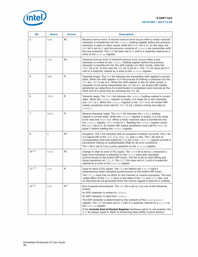
Bit Name Access Description
3 ROE RC Receive overrun error. A receive-overrun error occurs when a newly receivedcharacter is transferred into the rxdata holding register before the previouscharacter is read (in other words, while the RRDY bit is 1). In this case, theROE bit is set to 1, and the previous contents of rxdata are overwritten withthe new character. The ROE bit stays set to 1 until it is explicitly cleared by awrite to the status register.
4 TOE RC Transmit overrun error. A transmit-overrun error occurs when a newcharacter is written to the txdata holding register before the previouscharacter is transferred into the shift register (in other words, while theTRDY bit is 0). In this case the TOE bit is set to 1. The TOE bit stays set to 1until it is explicitly cleared by a write to the status register.
5 TMT R Transmit empty. The TMT bit indicates the transmitter shift register’s currentstate. When the shift register is in the process of shifting a character out theTXD pin, TMT is set to 0. When the shift register is idle (in other words, acharacter is not being transmitted) the TMT bit is 1. An Avalon-MM masterperipheral can determine if a transmission is completed (and received at theother end of a serial link) by checking the TMT bit.
6 TRDY R Transmit ready. The TRDY bit indicates the txdata holding register’s currentstate. When the txdata register is empty, it is ready for a new character,and TRDY is 1. When the txdata register is full, TRDY is 0. An Avalon-MMmaster peripheral must wait for TRDY to be 1 before writing new data totxdata.
7 RRDY R Receive character ready. The RRDY bit indicates the rxdata holdingregister’s current state. When the rxdata register is empty, it is not readyto be read and RRDY is 0. When a newly received value is transferred intothe rxdata register, RRDY is set to 1. Reading the rxdata register clearsthe RRDY bit to 0. An Avalon-MM master peripheral must wait for RRDY toequal 1 before reading the rxdata register.
8 E RC Exception. The E bit indicates that an exception condition occurred. The E bitis a logical-OR of the TOE, ROE, BRK, FE, and PE bits. The E bit and itscorresponding interrupt-enable bit (IE) bit in the control register provide aconvenient method to enable/disable IRQs for all error conditions.The E bit is set to 0 by a write operation to the status register.
10 (7) DCTS RC Change in clear to send (CTS) signal. The DCTS bit is set to 1 whenever alogic-level transition is detected on the CTS_N input port (sampledsynchronously to the Avalon-MM clock). This bit is set by both falling andrising transitions on CTS_N. The DCTS bit stays set to 1 until it is explicitlycleared by a write to the status register.
11 (7) CTS R Clear-to-send (CTS) signal. The CTS bit reflects the CTS_N input’sinstantaneous state (sampled synchronously to the Avalon-MM clock).The CTS_N input has no effect on the transmit or receive processes. The onlyvisible effect of the CTS_N input is the state of the CTS and DCTS bits, andan IRQ that can be generated when the control register’s idcts bit is enabled.
12 (7) EOP R(7) End of packet encountered. The EOP bit is set to 1 by one of the followingevents:An EOP character is written to txdataAn EOP character is read from rxdataThe EOP character is determined by the contents of the endofpacketregister. The EOP bit stays set to 1 until it is explicitly cleared by a write tothe status register.If the Include End-of-Packet Register hardware option is not enabled, theEOP bit always reads 0. Refer to Streaming Data (DMA) Control Section.
8 UART Core
UG-01085 | 2017.11.06
Embedded Peripherals IP User Guide98

8.5.3.4 control Register
The control register consists of individual bits, each controlling an aspect of theUART core's operation. The value in the control register can be read at any time.
Each bit in the control register enables an IRQ for a corresponding bit in thestatus register. When both a status bit and its corresponding interrupt-enable bitare 1, the core generates an IRQ.
Table 69. control Register Bits
Bit Name Access Description
0 IPE RW Enable interrupt for a parity error.
1 IFE RW Enable interrupt for a framing error.
2 IBRK RW Enable interrupt for a break detect.
3 IROE RW Enable interrupt for a receiver overrun error.
4 ITOE RW Enable interrupt for a transmitter overrun error.
5 ITMT RW Enable interrupt for a transmitter shift register empty.
6 ITRDY RW Enable interrupt for a transmission ready.
7 IRRDY RW Enable interrupt for a read ready.
8 IE RW Enable interrupt for an exception.
9 TRBK RW Transmit break. The TRBK bit allows an Avalon-MM master peripheral totransmit a break character over the TXD output. The TXD signal is forced to 0when the TRBK bit is set to 1. The TRBK bit overrides any logic level that thetransmitter logic would otherwise drive on the TXD output. The TRBK bitinterferes with any transmission in process. The Avalon-MM master peripheralmust set the TRBK bit back to 0 after an appropriate break period elapses.
10 IDCTS RW Enable interrupt for a change in CTS signal.
11(8) RTS RW Request to send (RTS) signal. The RTS bit directly feeds the RTS_N output.An Avalon-MM master peripheral can write the RTS bit at any time. The valueof the RTS bit only affects the RTS_N output; it has no effect on thetransmitter or receiver logic. Because the RTS_N output is logic negative,when the RTS bit is 1, a low logic-level (0) is driven on the RTS_N output.
12 IEOP RW Enable interrupt for end-of-packet condition.
8.5.3.5 divisor Register (Optional)
The value in the divisor register is used to generate the baud rate clock. Theeffective baud rate is determined by the formula:
Baud Rate = (Clock frequency) / (divisor + 1)
(7) This bit is optional and may not exist in hardware.
(8) This bit is optional and may not exist in hardware.
8 UART Core
UG-01085 | 2017.11.06
Embedded Peripherals IP User Guide99
The divisor register is an optional hardware feature. If the Baud Rate Can BeChanged By Software hardware option is not enabled, the divisor register doesnot exist. In this case, writing divisor has no effect, and reading divisor returnsan undefined value. For more information, refer to the Baud Rate Options section.
8.5.3.6 endofpacket Register (Optional)
The value in the endofpacket register determines the end-of-packet character forvariable-length DMA transactions. After reset, the default value is zero, which is theASCII null character (\0). For more information, refer to status Register bits for thedescription for the EOP bit.
The endofpacket register is an optional hardware feature. If the Include end-of-packet register hardware option is not enabled, the endofpacket register does notexist. In this case, writing endofpacket has no effect, and reading returns anundefined value.
8.5.4 Interrupt Behavior
The UART core outputs a single IRQ signal to the Avalon-MM interface, which canconnect to any master peripheral in the system, such as a Nios II processor. Themaster peripheral must read the status register to determine the cause of theinterrupt.
Every interrupt condition has an associated bit in the status register and aninterrupt-enable bit in the control register. When any of the interrupt conditionsoccur, the associated status bit is set to 1 and remains set until it is explicitlyacknowledged. The IRQ output is asserted when any of the status bits are set whilethe corresponding interrupt-enable bit is 1. A master peripheral can acknowledge theIRQ by clearing the status register.
At reset, all interrupt-enable bits are set to 0; therefore, the core cannot assert anIRQ until a master peripheral sets one or more of the interrupt-enable bits to 1.
All possible interrupt conditions are listed with their associated status and control(interrupt-enable) bits. Details of each interrupt condition are provided in the statusbit descriptions.
8.6 Document Revision History
Table 70. UART Core Revision History
Date and DocumentVersion
Version Changes
June 2016 2016.06.17 Removed content regarding Avalon-MM flow control.
December 2010 v10.1.0 Removed the “Device Support”, “Instantiating the Core in SOPC Builder”,and “Referenced Documents” sections.
July 2010 v10.0.0 No change from previous release.
November 2009 v9.1.0 No change from previous release.
continued...
8 UART Core
UG-01085 | 2017.11.06
Embedded Peripherals IP User Guide100

Date and DocumentVersion
Version Changes
March 2009 v9.0.0 Added description of a new parameter, Synchronizer stages.
November 2008 v8.1.0 Changed to 8-1/2 x 11 page size. No change to content.
May 2008 v8.0.0 No change from previous release.
8 UART Core
UG-01085 | 2017.11.06
Embedded Peripherals IP User Guide101
9 Intel FPGA Avalon Mailbox Core
9.1 Core Overview
In a multiprocessor design, each processor may be dedicated to perform a specifictask. Communication between processors becomes crucial if the tasks of eachindividual processor are interdependent. Communication between processors mayinvolve data passing or task control coordination to accomplish certain functions.
The Intel FPGA Avalon Mailbox component provides the medium of communicationbetween processors. It provides a “message” passing location between the sendingprocessor and receiving processor. The receiving processor is notified upon a messagearrival. The notification can be in the form of an interrupt issuing to the receivingprocessor or it can continue pooling for new messages by the receiving processor.
If more than two processors require “message” passing, multiple Mailboxes can beinstantiated between the two processors. Each Intel FPGA Avalon Mailbox correspondsto one direction message passing.
9.2 Functional Description
Intel FPGA Avalon Mailbox provides two 32-bit registers for message passing betweenprocessors, Command register (0x0) and Pointer register (0x1). The message senderprocessor and message receiver processor have individual Avalon Memory Mapped(Avalon-MM) interfaces to a Mailbox component. A write to the command register bythe sender processor indicates a pending message in the Mailbox and an interrupt willbe issued to the receiver processor. Upon retrieval of the message by the receiverprocessor via a read transaction, the message is consumed, Mailbox is empty. Thestatus register (0x2) is used to indicate if the Mailbox is full or empty.
The Mailbox Avalon-MM interface which receives messages, or identified as senderinterface, will back pressure the sender if there is message pending in the Mailbox.This will ensure every single message passed into the Mailbox is not overwritten. Uponmessage arrival, the receiving processor will then receive a level interrupt by theMailbox. The interrupt will hold high until the single message is retrieved from theMailbox via the Avalon-MM interface of receiving processor.
In addition, the Interrupt Masking Register (0x3) is writable by the Avalon-MMinterface to mask its dedicated interrupt output. For example, receiver interface will beable to set the mask bit to mask off the message pending interrupt generated byMailbox. Meanwhile, sender interface will be able to set the mask bit to mask off themessage space interrupt output.
UG-01085 | 2017.11.06
Intel Corporation. All rights reserved. Intel, the Intel logo, Altera, Arria, Cyclone, Enpirion, MAX, Nios, Quartusand Stratix words and logos are trademarks of Intel Corporation or its subsidiaries in the U.S. and/or othercountries. Intel warrants performance of its FPGA and semiconductor products to current specifications inaccordance with Intel's standard warranty, but reserves the right to make changes to any products and servicesat any time without notice. Intel assumes no responsibility or liability arising out of the application or use of anyinformation, product, or service described herein except as expressly agreed to in writing by Intel. Intelcustomers are advised to obtain the latest version of device specifications before relying on any publishedinformation and before placing orders for products or services.*Other names and brands may be claimed as the property of others.
ISO9001:2008Registered
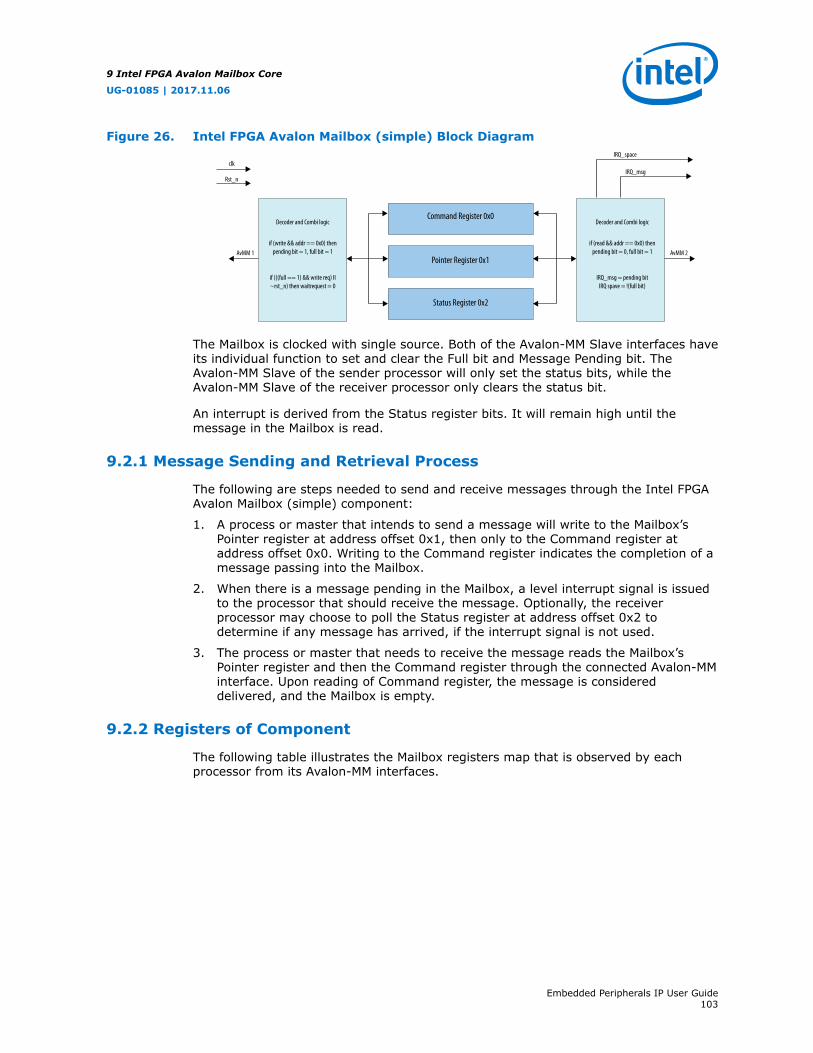
Figure 26. Intel FPGA Avalon Mailbox (simple) Block Diagram
Status Register 0x2
Pointer Register 0x1
Command Register 0x0
AvMM 1 AvMM 2
IRQ_space
IRQ_msg
Decoder and Combi logic Decoder and Combi logic
if (write && addr == 0x0) thenpending bit = 1, full bit = 1
if (((full == 1) && write req) II~rst_n) then waitrequest = 0
if (read && addr == 0x0) thenpending bit = 0, full bit = 1
IRQ_msg = pending bitIRQ spave = !(full bit)
clk
Rst_n
The Mailbox is clocked with single source. Both of the Avalon-MM Slave interfaces haveits individual function to set and clear the Full bit and Message Pending bit. TheAvalon-MM Slave of the sender processor will only set the status bits, while theAvalon-MM Slave of the receiver processor only clears the status bit.
An interrupt is derived from the Status register bits. It will remain high until themessage in the Mailbox is read.
9.2.1 Message Sending and Retrieval Process
The following are steps needed to send and receive messages through the Intel FPGAAvalon Mailbox (simple) component:
1. A process or master that intends to send a message will write to the Mailbox’sPointer register at address offset 0x1, then only to the Command register ataddress offset 0x0. Writing to the Command register indicates the completion of amessage passing into the Mailbox.
2. When there is a message pending in the Mailbox, a level interrupt signal is issuedto the processor that should receive the message. Optionally, the receiverprocessor may choose to poll the Status register at address offset 0x2 todetermine if any message has arrived, if the interrupt signal is not used.
3. The process or master that needs to receive the message reads the Mailbox’sPointer register and then the Command register through the connected Avalon-MMinterface. Upon reading of Command register, the message is considereddelivered, and the Mailbox is empty.
9.2.2 Registers of Component
The following table illustrates the Mailbox registers map that is observed by eachprocessor from its Avalon-MM interfaces.
9 Intel FPGA Avalon Mailbox Core
UG-01085 | 2017.11.06
Embedded Peripherals IP User Guide103

Table 71. Mailbox Register Map
Word Address Offset Register/ Queue Name Attribute
0x0 Command register R/W for sender, RO for receiver
0x1 Pointer register R/W for sender, RO for receiver
0x2 Status register RO
0x3 Interrupt Masking register Read (R) for both sender and receiver.Sender can only write to MessageSpace Interrupt Mask bit, Receiver canonly write to Message PendingInterrupt bit.
9.2.2.1 Command Register
The Command register is a 32-bit register which contains a user defined command tobe passed between processors. This register is read-writeable via Avalon-MM Slave(sender). However it is only readable by the Avalon-MM Slave (receiver) interface.
9.2.2.2 Pointer Register
Instead of passing huge data via the Mailbox, a Pointer register is introduced. ThePointer register contains the 32-bit address to the payload of the message. A payloadcould be the raw data to be passed to the receiving processor for further processing.However, a message could contain zero payload or data for processing. A write to thePointer may not be necessary for a message passing.
This register is read-writeable via Avalon-MM Slave (sender). However it is onlyreadable by Avalon-MM Slave (receiver) interface.
9.2.2.3 Status Register
The Status register presents the full or empty status of the Mailbox. As the Mailboxcan only contain one message at a time, the full bit status also indicates if there ismessage pending in the Mailbox. This register is read only by both Avalon-MM Slaveinterfaces.
Table 72. status Register Field
Bit Fields
31 ... ... ... ... ... 2 1 0
Reserved Mailbox full Messagepending
Table 73. Mailbox status Register Descriptions
Filed Name Description Reset Value
Message pending Value ‘0’ indicates the Mailbox has nomessage. Value ‘1’ indicates theMailbox has message pending forretrieval.
0
Mailbox full Value ‘1’ indicates the Mailbox is full.Value ‘0’ indicates Mailbox has spacefor incoming message.
0
Reserved - 0
9 Intel FPGA Avalon Mailbox Core
UG-01085 | 2017.11.06
Embedded Peripherals IP User Guide104
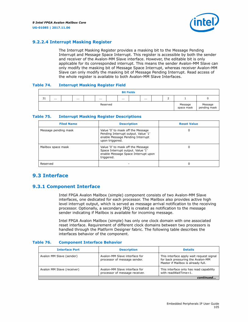
9.2.2.4 Interrupt Masking Register
The Interrupt Masking Register provides a masking bit to the Message PendingInterrupt and Message Space Interrupt. This register is accessible by both the senderand receiver of the Avalon-MM Slave interface. However, the editable bit is onlyapplicable for its conresponded interrupt. This means the sender Avalon-MM Slave canonly modify the masking bit of Message Space Interrupt, whereas receiver Avalon-MMSlave can only modify the masking bit of Message Pending Interrupt. Read access ofthe whole register is available to both Avalon-MM Slave Interfaces.
Table 74. Interrupt Masking Register Field
Bit Fields
31 ... ... ... ... ... 2 1 0
Reserved Messagespace mask
Messagepending mask
Table 75. Interrupt Masking Register Descriptions
Filed Name Description Reset Value
Message pending mask Value ‘0’ to mask off the MessagePending Interrupt output. Value ‘1’enable Message Pending Interruptupon triggered.
0
Mailbox space mask Value ‘0’ to mask off the MessageSpace Interrupt output. Value ‘1’enable Message Space Interrupt upontriggered.
0
Reserved - 0
9.3 Interface
9.3.1 Component Interface
Intel FPGA Avalon Mailbox (simple) component consists of two Avalon-MM Slaveinterfaces, one dedicated for each processor. The Mailbox also provides active highlevel interrupt output, which is served as message arrival notification to the receivingprocessor. Optionally, a secondary IRQ is created as notification to the messagesender indicating if Mailbox is available for incoming message.
Intel FPGA Avalon Mailbox (simple) has only one clock domain with one associatedreset interface. Requirement of different clock domains between two processors ishandled through the Platform Designer fabric. The following table describes theinterfaces behavior of the component.
Table 76. Component Interface Behavior
Interface Port Description Details
Avalon MM Slave (sender) Avalon-MM Slave interface forprocessor of message sender.
This interface apply wait request signalfor back pressuring the Avalon-MMMaster if Mailbox is already full.
Avalon MM Slave (receiver) Avalon-MM Slave interface forprocessor of message receiver.
This interface only has read capabilitywith readWaitTime=1.
continued...
9 Intel FPGA Avalon Mailbox Core
UG-01085 | 2017.11.06
Embedded Peripherals IP User Guide105
Interface Port Description Details
Clock Clock input of component. It supports maximum frequency up to400MHz on CycloneIV and 600MHz inStratixIV devices.
Reset_n Active LOW reset input/s. Support asynchronous reset assertion.De-assertion of reset has to besynchronized to the input clock.
IRQ_msg Message Pending Interrupt output toprocessor of message receiver uponmessage arrival. The signal will remainhigh until the message is retrieved.
Interrupt assertion and deassertion issynchronized to input clock.
IRQ_space Message Space Interrupt outputprocessor of message sender wheneverMailbox has space for incomingmessage. The signal will assert high aslong as the Mailbox is yet full.
Interrupt assertion and deassertion issynchronized to input clock. Theconnection of this interrupt port to thetop level is depends on configurationparameter of MSG_SPACE_NOTIFY.
9.3.2 Component Parameterization
Table 77. Intel FPGA Avalon Mailbox (simple) TCL Component ConfigurationParameters
Parameter Name Description Default Value Allowable Range
MSG_SPACE_NOTIFY Boolean ‘true’ will enable interruptoutput to message sending processorfor indicating available space forincoming message
0 0, 1
MSG_ARRIVAL_NOTIFY Boolean ‘true’ will enable interruptoutput to message receiver processorfor indicating a message is pendingfor retrieval.
1 0, 1
9 Intel FPGA Avalon Mailbox Core
UG-01085 | 2017.11.06
Embedded Peripherals IP User Guide106
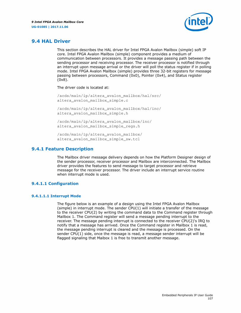
9.4 HAL Driver
This section describes the HAL driver for Intel FPGA Avalon Mailbox (simple) soft IPcore. Intel FPGA Avalon Mailbox (simple) component provides a medium ofcommunication between processors. It provides a message passing path between thesending processor and receiving processor. The receiver processor is notified throughan interrupt upon message arrival or the driver will poll the status register if in pollingmode. Intel FPGA Avalon Mailbox (simple) provides three 32-bit registers for messagepassing between processors, Command (0x0), Pointer (0x4), and Status register(0x8).
The driver code is located at:
/acds/main/ip/altera_avalon_mailbox/hal/src/altera_avalon_mailbox_simple.c
/acds/main/ip/altera_avalon_mailbox/hal/inc/altera_avalon_mailbox_simple.h
/acds/main/ip/altera_avalon_mailbox/inc/altera_avalon_mailbox_simple_regs.h
/acds/main/ip/altera_avalon_mailbox/altera_avalon_mailbox_simple_sw.tcl
9.4.1 Feature Description
The Mailbox driver message delivery depends on how the Platform Designer design ofthe sender processor, receiver processor and Mailbox are interconnected. The Mailboxdriver provides the features to send message to target processor and retrievemessage for the receiver processor. The driver include an interrupt service routinewhen interrupt mode is used.
9.4.1.1 Configuration
9.4.1.1.1 Interrupt Mode
The figure below is an example of a design using the Intel FPGA Avalon Mailbox(simple) in interrupt mode. The sender CPU(1) will initiate a transfer of the messageto the receiver CPU(2) by writing the command data to the Command register throughMailbox 1. The Command register will send a message pending interrupt to thereceiver. The message pending interrupt is connected to the receiver CPU(2)'s IRQ tonotify that a message has arrived. Once the Command register in Mailbox 1 is read,the message pending interrupt is cleared and the message is processed. On thesender CPU(1) side, once the message is read, a message sender interrupt will beflagged signaling that Maibox 1 is free to transmit another message.
9 Intel FPGA Avalon Mailbox Core
UG-01085 | 2017.11.06
Embedded Peripherals IP User Guide107
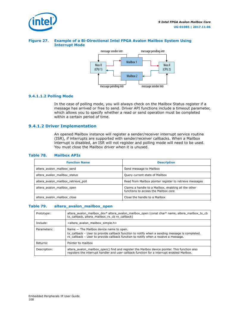
Figure 27. Example of a Bi-Directional Intel FPGA Avalon Mailbox System UsingInterrupt Mode
message sender intr
message sender intr
message pending intr
message pending intr
Nios II(CPU 1)
Nios II(CPU 2)
Mailbox 1
Mailbox 2
9.4.1.1.2 Polling Mode
In the case of polling mode, you will always check on the Mailbox Status register if amessage has arrived or free to send. Driver API functions include a timeout parameter,which allows you to specify whether a read or send operation must be completedwithin a certain period of time.
9.4.1.2 Driver Implementation
An opened Mailbox instance will register a sender/receiver interrupt service routine(ISR), if interrupts are supported with sender/receiver callbacks. When a Mailboxinterrupt is disabled, an ISR will not register and polling mode will need to be used.You must close the Mailbox driver when it is unused.
Table 78. Mailbox APIs
Function Name Description
altera_avalon_mailbox_send Send message to Mailbox
altera_avalon_mailbox_status Query current state of Mailbox
altera_avalon_mailbox_retrieve_poll Read from Mailbox pointer register to retrieve messages
altera_avalon_mailbox_open Claims a handle to a Mailbox, enabling all the otherfunctions to access the Mailbox core
altera_avalon_mailbox_close Close the handle to a Mailbox
Table 79. altera_avalon_mailbox_open
Prototype: altera_avalon_mailbox_dev* altera_avalon_mailbox_open (const char* name, altera_mailbox_tx_cbtx_callback, altera_mailbox_rx_cb rx_callback)
Include: <altera_avalon_mailbox_simple.h>
Parameters: Name — The Mailbox device name to open.tx_callback – User to provide callback function to notify when a sending message is completed.rx_callback – User to provide callback function to notify when a receive a message.
Returns: Pointer to mailbox
Description: altera_avalon_mailbox_open() find and register the Mailbox device pointer. This function alsoregisters the interrupt handler and user callback function for a interrupt enabled Mailbox.
9 Intel FPGA Avalon Mailbox Core
UG-01085 | 2017.11.06
Embedded Peripherals IP User Guide108

Table 80. altera_avalon_mailbox_close
Prototype: void altera_avalon_mailbox_close (altera_avalon_mailbox_dev* dev);
Include: <altera_avalon_mailbox_simple.h>
Parameters: dev—The Mailbox to close.
Returns: Null
Description: alt_avalon_mailbox_close() closes the mailbox de-registering interrupt handler and callbackfunctions and masking Mailbox interrupt.
Table 81. altera_avalon_mailbox_send
Prototype: int altera_avalon_mailbox_send (altera_avalon_mailbox_dev* dev, void* message, int timeout,EventType event)
Include: <altera_avalon_mailbox_simple.h>
Parameters: *message – Pointer to message command and pointer structure.Timeout – Specifies number of loops before sending a message. Give a ‘0’ value to wait until themessage is transferred.EventType – set ‘POLL’ or ‘ISR’.
Returns: Return 0 on success and 1 for fail.
Description: altera_avalon_mailbox_send () sends a message to the mailbox. This is a blocking function when thesender interrupt is disabled.This function is in non-blocking when interrupt is enabled.
Table 82. altera_avalon_mailbox_retrieve_poll
Prototype: int altera_avalon_mailbox_retrieve_poll (altera_avalon_mailbox_dev* dev,alt_u32* msg_ptr, alt_u32timeout)
Include: <altera_avalon_mailbox_simple.h>
Parameters: dev - The Mailbox device to read message from.timeout – Specifies number loops before sending a message. Give a ‘0’ value to wait until a messageis retrieved.msg_ptr – A pointer to an array of two Dwords which are for the command and message pointer.This pointer will be populated with a receive message if successful or NULL if error.
Returns: Return pointer to message and command. Return ‘NULL’ in messages if timeout. This is a blockingfunction.
Description: altera_avalon_mailbox_retrieve_poll () reads a message pointer and command to Mailbox structurefrom the Mailbox and notifies through callback.
Table 83. altera_avalon_mailbox_status
Prototype: alt_u32 altera_avalon_mailbox_status (altera_avalon_mailbox_dev* dev)
Include: <altera_avalon_mailbox_simple.h>
Parameters: dev -The Mailbox device to read status from
Returns: For a receiving Mailbox:- 0 for no message pending- 1 for message pendingFor a sending Mailbox:- 0 for Mailbox empty (ready to send)- 1 for Mailbox full (not ready to send)
Description: Indicates to sender Mailbox it is full or empty for transfer.Indicates to receiver Mailbox has a message pending or not.
9 Intel FPGA Avalon Mailbox Core
UG-01085 | 2017.11.06
Embedded Peripherals IP User Guide109

Example 6. Device structure
// Callback routine type definitiontypedef void(*altera_mailbox_rx_cb)(void *message);typedefvoid (*altera_mailbox_tx_cb)(void *message,int status);
typedef enum mbox_type { MBOX_TX = 0,MBOX_RX } MboxType;typedef enum event_type { ISR = 0, POLL } EventType;
typedef struct altera_avalon_mailbox_dev{ alt_dev dev; /* Device linke-list entry */ alt_u32 base; /* Base address of Mailbox */ alt_u32 mailbox_irq; /* Mailbox IRQ */ alt_u32 mailbox_intr_ctrl_id; /* Mailbox IRQ ID */ altera_mailbox_tx_cb tx_cb; /* Callback routine pointer */ altera_mailbox_rx_cb rx_cb; /* Callback routine pointer */ MboxType mbox_type; /* Mailbox direction */ alt_u32* mbox_msg; /* a pointer to message array to be received or sent */ alt_u8 lock; /* Token to indicate mbox_msg already taken */ ALT_SEM (write_lock) /* Semaphore used to control access to the write in multi-threaded mode */} altera_avalon_mailbox_dev;
9.4.1.3 Driver Examples
The figure below demonstrates writing to a Mailbox. For this example, assume that thehardware system has two processors communicating via Mailboxes. The systemincludes two Mailbox cores, which provides two-way communication between theprocessors.
Example 7. Sender Processor Using Mailbox to Send a Message.
#include <stdio.h>#include "altera_avalon_mailbox_simple.h"#include "altera_avalon_mailbox_simple_regs.h"#include "system.h"
/* example callback function from users*/void tx_cb (void* report, int status) { if (!status) { printf (“Transfer done”); } else { printf (“error in transfer”); }
int main_sender()
9 Intel FPGA Avalon Mailbox Core
UG-01085 | 2017.11.06
Embedded Peripherals IP User Guide110
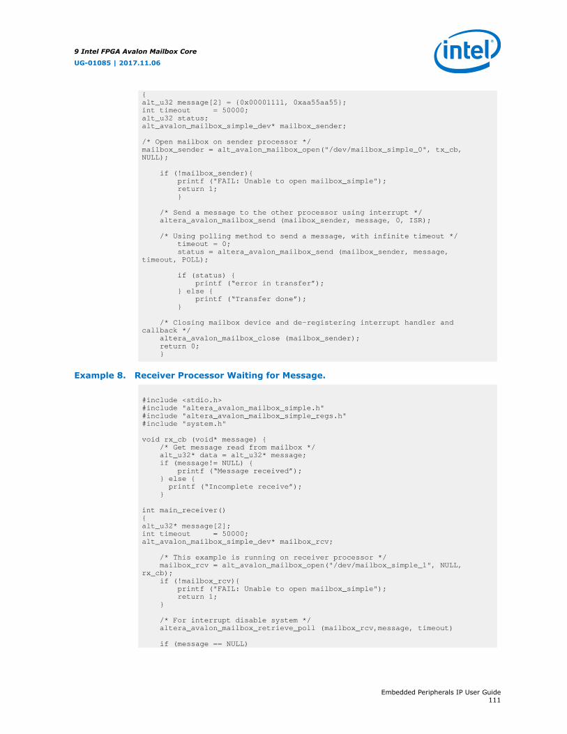
{alt_u32 message[2] = {0x00001111, 0xaa55aa55};int timeout = 50000;alt_u32 status;alt_avalon_mailbox_simple_dev* mailbox_sender;
/* Open mailbox on sender processor */mailbox_sender = alt_avalon_mailbox_open("/dev/mailbox_simple_0", tx_cb, NULL);
if (!mailbox_sender){ printf ("FAIL: Unable to open mailbox_simple"); return 1; }
/* Send a message to the other processor using interrupt */ altera_avalon_mailbox_send (mailbox_sender, message, 0, ISR);
/* Using polling method to send a message, with infinite timeout */ timeout = 0; status = altera_avalon_mailbox_send (mailbox_sender, message, timeout, POLL);
if (status) { printf (“error in transfer”); } else { printf (“Transfer done”); }
/* Closing mailbox device and de-registering interrupt handler and callback */ altera_avalon_mailbox_close (mailbox_sender); return 0; }
Example 8. Receiver Processor Waiting for Message.
#include <stdio.h>#include "altera_avalon_mailbox_simple.h"#include "altera_avalon_mailbox_simple_regs.h"#include "system.h"
void rx_cb (void* message) { /* Get message read from mailbox */ alt_u32* data = alt_u32* message; if (message!= NULL) { printf (“Message received”); } else { printf (“Incomplete receive”); }
int main_receiver(){alt_u32* message[2];int timeout = 50000;alt_avalon_mailbox_simple_dev* mailbox_rcv;
/* This example is running on receiver processor */ mailbox_rcv = alt_avalon_mailbox_open("/dev/mailbox_simple_1", NULL, rx_cb); if (!mailbox_rcv){ printf ("FAIL: Unable to open mailbox_simple"); return 1; }
/* For interrupt disable system */ altera_avalon_mailbox_retrieve_poll (mailbox_rcv,message, timeout) if (message == NULL)
9 Intel FPGA Avalon Mailbox Core
UG-01085 | 2017.11.06
Embedded Peripherals IP User Guide111
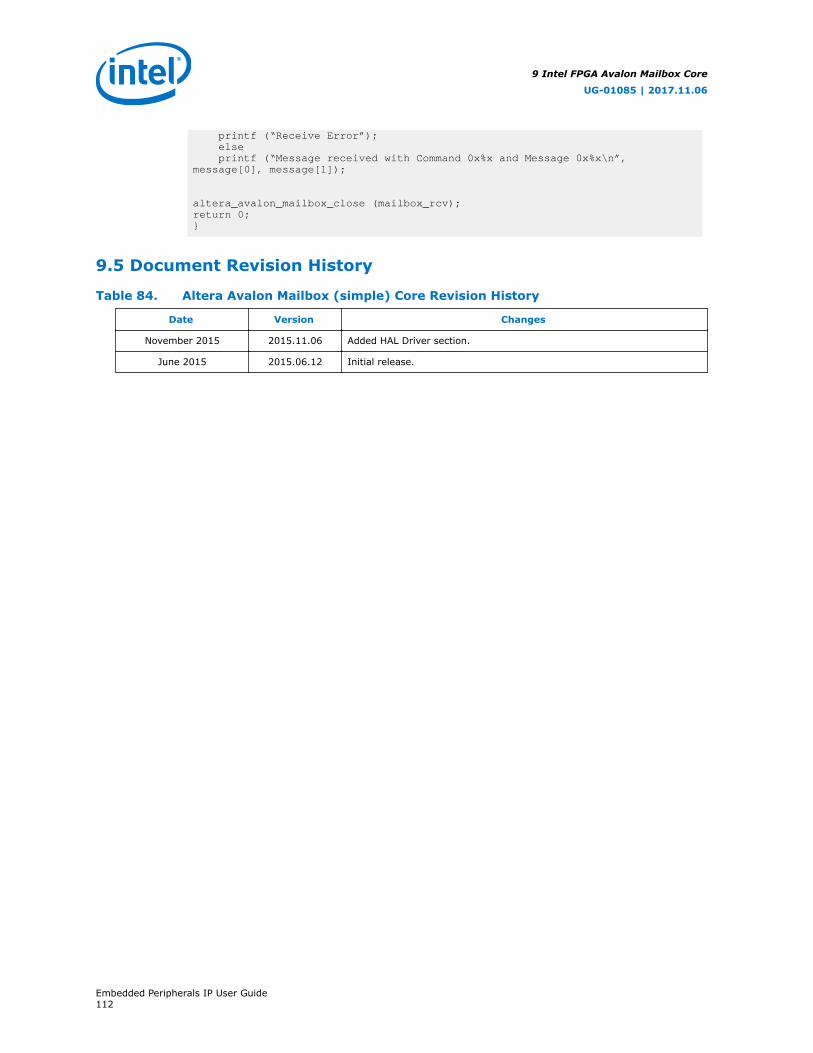
printf (“Receive Error”); else printf (“Message received with Command 0x%x and Message 0x%x\n”, message[0], message[1]);
altera_avalon_mailbox_close (mailbox_rcv);return 0;}
9.5 Document Revision History
Table 84. Altera Avalon Mailbox (simple) Core Revision History
Date Version Changes
November 2015 2015.11.06 Added HAL Driver section.
June 2015 2015.06.12 Initial release.
9 Intel FPGA Avalon Mailbox Core
UG-01085 | 2017.11.06
Embedded Peripherals IP User Guide112
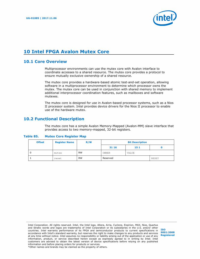
10 Intel FPGA Avalon Mutex Core
10.1 Core Overview
Multiprocessor environments can use the mutex core with Avalon interface tocoordinate accesses to a shared resource. The mutex core provides a protocol toensure mutually exclusive ownership of a shared resource.
The mutex core provides a hardware-based atomic test-and-set operation, allowingsoftware in a multiprocessor environment to determine which processor owns themutex. The mutex core can be used in conjunction with shared memory to implementadditional interprocessor coordination features, such as mailboxes and softwaremutexes.
The mutex core is designed for use in Avalon-based processor systems, such as a NiosII processor system. Intel provides device drivers for the Nios II processor to enableuse of the hardware mutex.
10.2 Functional Description
The mutex core has a simple Avalon Memory-Mapped (Avalon-MM) slave interface thatprovides access to two memory-mapped, 32-bit registers.
Table 85. Mutex Core Register Map
Offset Register Name R/W Bit Description
31 16 15 1 0
0 mutex RW OWNER VALUE
1 reset RW Reserved RESET
UG-01085 | 2017.11.06
Intel Corporation. All rights reserved. Intel, the Intel logo, Altera, Arria, Cyclone, Enpirion, MAX, Nios, Quartusand Stratix words and logos are trademarks of Intel Corporation or its subsidiaries in the U.S. and/or othercountries. Intel warrants performance of its FPGA and semiconductor products to current specifications inaccordance with Intel's standard warranty, but reserves the right to make changes to any products and servicesat any time without notice. Intel assumes no responsibility or liability arising out of the application or use of anyinformation, product, or service described herein except as expressly agreed to in writing by Intel. Intelcustomers are advised to obtain the latest version of device specifications before relying on any publishedinformation and before placing orders for products or services.*Other names and brands may be claimed as the property of others.
ISO9001:2008Registered

The mutex core has the following basic behavior. This description assumes there aremultiple processors accessing a single mutex core, and each processor has a uniqueidentifier (ID).
• When the VALUE field is 0x0000, the mutex is unlocked and available. Otherwise,the mutex is locked and unavailable.
• The mutex register is always readable. Avalon-MM master peripherals, such as aprocessor, can read the mutex register to determine its current state.
• The mutex register is writable only under specific conditions. A write operationchanges the mutex register only if one or both of the following conditions aretrue:
— The VALUE field of the mutex register is zero.
— The OWNER field of the mutex register matches the OWNER field in the data tobe written.
• A processor attempts to acquire the mutex by writing its ID to the OWNER field,and writing a non-zero value to the VALUE field. The processor then checks if theacquisition succeeded by verifying the OWNER field.
• After system reset, the RESET bit in the reset register is high. Writing a one tothis bit clears it.
10.3 Configuration
The MegaWizard™ Interface provides the following options:
• Initial Value—the initial contents of the VALUE field after reset. If the InitialValue setting is non-zero, you must also specify Initial Owner.
• Initial Owner—the initial contents of the OWNER field after reset. When InitialOwner is specified, this owner must release the mutex before it can be acquiredby another owner.
10.4 Software Programming Model
The following sections describe the software programming model for the mutex core.For Nios II processor users, Intel provides routines to access the mutex corehardware. These functions are specific to the mutex core and directly manipulate low-level hardware. The mutex core cannot be accessed via the HAL API or the ANSI Cstandard library. In Nios II processor systems, a processor locks the mutex by writingthe value of its cpuid control register to the OWNER field of the mutex register.
10.4.1 Software Files
Intel provides the following software files accompanying the mutex core:
• altera_avalon_mutex_regs.h—Defines the core's register map, providingsymbolic constants to access the low-level hardware.
• altera_avalon_mutex.h—Defines data structures and functions to access themutex core hardware.
• altera_avalon_mutex.c—Contains the implementations of the functions toaccess the mutex core
10 Intel FPGA Avalon Mutex Core
UG-01085 | 2017.11.06
Embedded Peripherals IP User Guide114

10.4.2 Hardware Access Routines
This section describes the low-level software constructs for manipulating the mutexcore. The file altera_avalon_mutex.h declares a structure alt_mutex_dev thatrepresents an instance of a mutex device. It also declares routines for accessing themutex hardware structure, listed in the table below.
Table 86. Hardware Access Routines
Function Name Description
altera_avalon_mutex_open() Claims a handle to a mutex, enabling all the other functionsto access the mutex core.
altera_avalon_mutex_trylock() Tries to lock the mutex. Returns immediately if it fails tolock the mutex.
altera_avalon_mutex_lock() Locks the mutex. Will not return until it has successfullyclaimed the mutex.
altera_avalon_mutex_unlock() Unlocks the mutex.
altera_avalon_mutex_is_mine() Determines if this CPU owns the mutex.
altera_avalon_mutex_first_lock() Tests whether the mutex has been released since reset.
These routines coordinate access to the software mutex structure using a hardwaremutex core. For a complete description of each function, see section the Mutex APIsection.
The code shown in below demonstrates opening a mutex device handle and locking amutex.
#include <altera_avalon_mutex.h>
/* get the mutex device handle */alt_mutex_dev* mutex = altera_avalon_mutex_open( “/dev/mutex” );
/* acquire the mutex, setting the value to one */altera_avalon_mutex_lock( mutex, 1 );
/* * Access a shared resource here. */
/* release the lock */
altera_avalon_mutex_unlock( mutex );
10.5 Mutex API
This section describes the application programming interface (API) for the mutex core.
10.5.1 altera_avalon_mutex_is_mine()
Prototype: int altera_avalon_mutex_is_mine(alt_mutex_dev* dev)
Thread-safe: Yes.
continued...
10 Intel FPGA Avalon Mutex Core
UG-01085 | 2017.11.06
Embedded Peripherals IP User Guide115
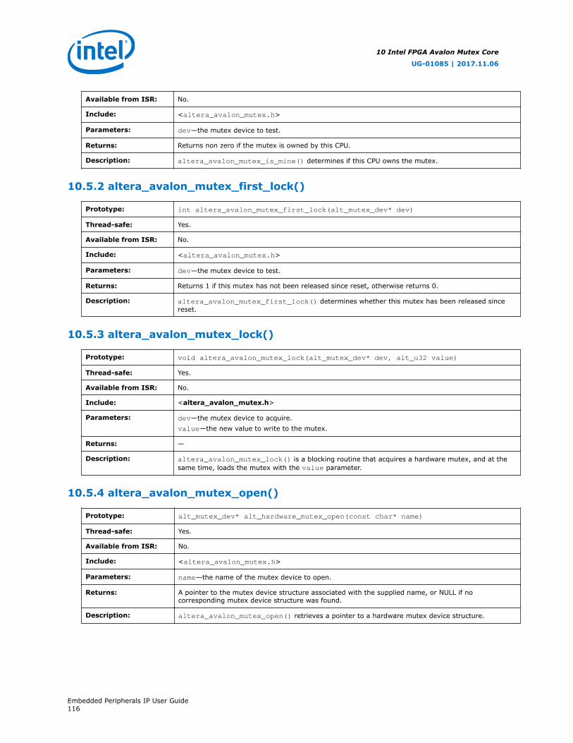
Available from ISR: No.
Include: <altera_avalon_mutex.h>
Parameters: dev—the mutex device to test.
Returns: Returns non zero if the mutex is owned by this CPU.
Description: altera_avalon_mutex_is_mine() determines if this CPU owns the mutex.
10.5.2 altera_avalon_mutex_first_lock()
Prototype: int altera_avalon_mutex_first_lock(alt_mutex_dev* dev)
Thread-safe: Yes.
Available from ISR: No.
Include: <altera_avalon_mutex.h>
Parameters: dev—the mutex device to test.
Returns: Returns 1 if this mutex has not been released since reset, otherwise returns 0.
Description: altera_avalon_mutex_first_lock() determines whether this mutex has been released sincereset.
10.5.3 altera_avalon_mutex_lock()
Prototype: void altera_avalon_mutex_lock(alt_mutex_dev* dev, alt_u32 value)
Thread-safe: Yes.
Available from ISR: No.
Include: <altera_avalon_mutex.h>
Parameters: dev—the mutex device to acquire.value—the new value to write to the mutex.
Returns: —
Description: altera_avalon_mutex_lock() is a blocking routine that acquires a hardware mutex, and at thesame time, loads the mutex with the value parameter.
10.5.4 altera_avalon_mutex_open()
Prototype: alt_mutex_dev* alt_hardware_mutex_open(const char* name)
Thread-safe: Yes.
Available from ISR: No.
Include: <altera_avalon_mutex.h>
Parameters: name—the name of the mutex device to open.
Returns: A pointer to the mutex device structure associated with the supplied name, or NULL if nocorresponding mutex device structure was found.
Description: altera_avalon_mutex_open() retrieves a pointer to a hardware mutex device structure.
10 Intel FPGA Avalon Mutex Core
UG-01085 | 2017.11.06
Embedded Peripherals IP User Guide116
10.5.5 altera_avalon_mutex_trylock()
Prototype: int altera_avalon_mutex_trylock(alt_mutex_dev* dev, alt_u32 value)
Thread-safe: Yes.
Available from ISR: No.
Include: <altera_avalon_mutex.h>
Parameters: dev—the mutex device to lock.value—the new value to write to the mutex.
Returns: 0 = The mutex was successfully locked.Others = The mutex was not locked.
Description: altera_avalon_mutex_trylock() tries once to lock the hardware mutex, and returns immediately.
10.5.6 altera_avalon_mutex_unlock()
Prototype: void altera_avalon_mutex_unlock(alt_mutex_dev* dev)
Thread-safe: Yes.
Available from ISR: No.
Include: <altera_avalon_mutex.h>
Parameters: dev—the mutex device to unlock.
Returns: Null.
Description: altera_avalon_mutex_unlock() releases a hardware mutex device. Upon release, the valuestored in the mutex is set to zero. If the caller does not hold the mutex, the behavior of this function isundefined.
10.6 Document Revision History
Table 87. Mutex Core Revision History
Date Version Changes
July 2014 2014.07.24 Removed mention of SOPC Builder, updated to Platform Designer
December 2010 v10.1.0 Removed the “Device Support”, “Instantiating the Core in SOPC Builder”,and “Referenced Documents” sections.
July 2010 v10.0.0 No change from previous release.
November 2009 v9.1.0 No change from previous release.
March 2009 v9.0.0 No change from previous release.
November 2008 v8.1.0 Changed to 8-1/2 x 11 page size. No change to content.
May 2008 v8.0.0 No change from previous release.
10 Intel FPGA Avalon Mutex Core
UG-01085 | 2017.11.06
Embedded Peripherals IP User Guide117
11 Intel FPGA Avalon I2C (Master) Core
11.1 Core Overview
The Intel FPGA Avalon I2C (Master) core (altera_avalon_i2c ) is an IP whichimplements the I2C protocol. It supports only master mode with a bit rate (fast mode)of 400 kbits/s and it can also operate in a multi-master system. It has an AvalonMemory-Mapped (Avalon-MM) slave interface for a host processor to access its control,status, command and data FIFO. Configure the command and data FIFO to beaccessed by either the Avalon-MM or the Avalon Streaming (Avalon-ST). On the serialinterface side, it provides two data and clock lines to communicate to remote I2Cdevices.
11.2 Feature Description
11.2.1 Supported Features
• Supports I2C master mode
• Supports I2C standard mode (100 kbits/s) and fast mode (400 kbits/s)
• Supports multi-master operation
• Supports 7 bit or 10 bit addressing
• Supports START, repeated START and STOP generation
• Run time programmable SCL low and high period
• Interrupt or polled-mode of operation
• Avalon-MM slave interface for CSR registers access
• Avalon-MM or Avalon-ST for command and receive data FIFO access
11.2.2 Unsupported Features
I2C slave mode is not supported at the moment. Refer to Intel FPGA I2C Slave toAvalon MM Master Bridge IP for an I2C slave solution.
Related Links
Intel FPGA I2C Slave to Avalon-MM Master Bridge Core on page 133
11.3 Configuration Parameters
Configure the following parameters through Platform Designer.
UG-01085 | 2017.11.06
Intel Corporation. All rights reserved. Intel, the Intel logo, Altera, Arria, Cyclone, Enpirion, MAX, Nios, Quartusand Stratix words and logos are trademarks of Intel Corporation or its subsidiaries in the U.S. and/or othercountries. Intel warrants performance of its FPGA and semiconductor products to current specifications inaccordance with Intel's standard warranty, but reserves the right to make changes to any products and servicesat any time without notice. Intel assumes no responsibility or liability arising out of the application or use of anyinformation, product, or service described herein except as expressly agreed to in writing by Intel. Intelcustomers are advised to obtain the latest version of device specifications before relying on any publishedinformation and before placing orders for products or services.*Other names and brands may be claimed as the property of others.
ISO9001:2008Registered
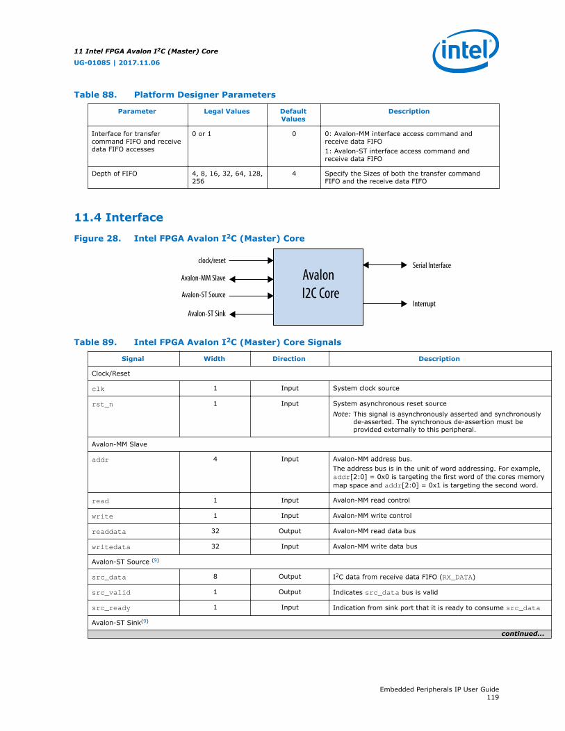
Table 88. Platform Designer Parameters
Parameter Legal Values DefaultValues
Description
Interface for transfercommand FIFO and receivedata FIFO accesses
0 or 1 0 0: Avalon-MM interface access command andreceive data FIFO1: Avalon-ST interface access command andreceive data FIFO
Depth of FIFO 4, 8, 16, 32, 64, 128,256
4 Specify the Sizes of both the transfer commandFIFO and the receive data FIFO
11.4 Interface
Figure 28. Intel FPGA Avalon I2C (Master) Core
clock/reset
Avalon-MM Slave
Avalon-ST Source
Avalon-ST Sink
Serial Interface
Interrupt
Avalon I2C Core
Table 89. Intel FPGA Avalon I2C (Master) Core Signals
Signal Width Direction Description
Clock/Reset
clk 1 Input System clock source
rst_n 1 Input System asynchronous reset sourceNote: This signal is asynchronously asserted and synchronously
de-asserted. The synchronous de-assertion must beprovided externally to this peripheral.
Avalon-MM Slave
addr 4 Input Avalon-MM address bus.The address bus is in the unit of word addressing. For example,addr[2:0] = 0x0 is targeting the first word of the cores memorymap space and addr[2:0] = 0x1 is targeting the second word.
read 1 Input Avalon-MM read control
write 1 Input Avalon-MM write control
readdata 32 Output Avalon-MM read data bus
writedata 32 Input Avalon-MM write data bus
Avalon-ST Source (9)
src_data 8 Output I2C data from receive data FIFO (RX_DATA)
src_valid 1 Output Indicates src_data bus is valid
src_ready 1 Input Indication from sink port that it is ready to consume src_data
Avalon-ST Sink(9)
continued...
11 Intel FPGA Avalon I2C (Master) Core
UG-01085 | 2017.11.06
Embedded Peripherals IP User Guide119
Signal Width Direction Description
snk_data 10 Input 10-bit value driven by source port to transfer command FIFO(TFR_CMD)
snk_valid 1 Input Indication from source port that snk_data is valid
snk_ready 1 Output Indication from sink port that it is ready to consume snk_data
Serial Interface
scl_oe 1 Output Output enable for open drain buffer that drives SCL pin1: SCL line pulled low0: Open drain buffer is tri-stated and SCL line is externally pulledhigh
sda_oe 1 Output Output enable for open drain buffer that drives SDA pin1: SDA line pulled low0: Open drain buffer is tri-stated and SDA line is externallypulled high
scl_in 1 Input Input path of I2C’s open drain buffer
sda_in 1 Input It is from input path of I2C’s open drain buffer
Interrupt
intr 1 Output Active high level interrupt output to host processor
11.5 Registers
11.5.1 Register Memory Map
Note: Each address offset represent 1 word of memory address space.
Table 90. Register Memory Map
Name Address offset Description
TFR_CMD 0x0 Transfer command FIFO
RX_DATA 0x1 Receive data FIFO
CTRL 0x2 Control register
ISER 0x3 Interrupt status enable register
ISR 0x4 Interrupt status register
STATUS 0x5 Status register
TFR_CMD_FIFO_LVL 0x6 TFR_CMD FIFO level register
RX_DATA_FIFO_LVL 0x7 RX_DATA FIFO level register
continued...
(9) These signals are not used if “Interface for transfer command FIFO and receive data FIFOaccesses” is set to Avalon-MM Slave. This setting can be configured through Platform Designer.
11 Intel FPGA Avalon I2C (Master) Core
UG-01085 | 2017.11.06
Embedded Peripherals IP User Guide120
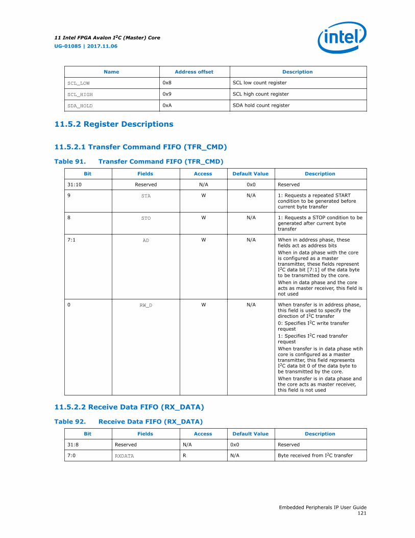
Name Address offset Description
SCL_LOW 0x8 SCL low count register
SCL_HIGH 0x9 SCL high count register
SDA_HOLD 0xA SDA hold count register
11.5.2 Register Descriptions
11.5.2.1 Transfer Command FIFO (TFR_CMD)
Table 91. Transfer Command FIFO (TFR_CMD)
Bit Fields Access Default Value Description
31:10 Reserved N/A 0x0 Reserved
9 STA W N/A 1: Requests a repeated STARTcondition to be generated beforecurrent byte transfer
8 STO W N/A 1: Requests a STOP condition to begenerated after current bytetransfer
7:1 AD W N/A When in address phase, thesefields act as address bitsWhen in data phase with the coreis configured as a mastertransmitter, these fields representI2C data bit [7:1] of the data byteto be transmitted by the core.When in data phase and the coreacts as master receiver, this field isnot used
0 RW_D W N/A When transfer is in address phase,this field is used to specify thedirection of I2C transfer0: Specifies I2C write transferrequest1: Specifies I2C read transferrequestWhen transfer is in data phase wtihcore is configured as a mastertransmitter, this field representsI2C data bit 0 of the data byte tobe transmitted by the core.When transfer is in data phase andthe core acts as master receiver,this field is not used
11.5.2.2 Receive Data FIFO (RX_DATA)
Table 92. Receive Data FIFO (RX_DATA)
Bit Fields Access Default Value Description
31:8 Reserved N/A 0x0 Reserved
7:0 RXDATA R N/A Byte received from I2C transfer
11 Intel FPGA Avalon I2C (Master) Core
UG-01085 | 2017.11.06
Embedded Peripherals IP User Guide121

11.5.2.3 Control Register (CTRL)
Bit Fields Access Default Value Description
31:6 Reserved N/A 0x0 Reserved
5:4 RX_DATA_FIFO_THD R/W 0x0 Threshold level of the receive dataFIFONote: If the actual level is equal
or more than the thresholdlevel, RX_READY interruptstatus bit is asserted.
0x3: RX_DATA FIFO is full0x2: RX_DATA FIFO is ½ full0x1: RX_DATA FIFO is ¼ full0x0: 1 valid entry
3:2 TFR_CMD_FIFO_THD R/W 0x0 Threshold level of the transfercommand FIFONote: If the actual level is equal
or less than the thresholdlevel, TX_READY interruptstatus bit is asserted.
0x3: TFR_CMD FIFO is not full (hasat least one empty entry)0x2: TFR_CMD FIFO is ½ full0x1: TFR_CMD FIFO is ¼ full0x0: TFR_CMD FIFO is empty
1 BUS_SPEED R/W 0x0 Bus speed1: Fast mode (up to 400 kbits/s)0: Standard mode (up to 100kbits/s)
0 EN R/W 0x0 The core enable bit1: Core is enabled0: Core is disabled
11.5.2.4 Interrupt Status Enable Register (ISER)
Table 93. Interrupt Status Enable Register (ISER)
Bit Fields Access Default Value Description
31:5 Reserved N/A 0x0 Reserved
4 RX_OVER_EN R/W 0x0 1: Enable interrupt for RX_OVERcondition
3 ARBLOST_DET_EN R/W 0x0 1: Enable interrupt forARBLOST_DET condition
2 NACK_DET_EN R/W 0x0 1: Enable interrupt for NACK_DETcondition
1 RX_READY_EN R/W 0x0 1: Enable interrupt for RX_READYcondition
0 TX_READY_EN R/W 0x0 1: Enable interrupt for TX_READYcondition
11 Intel FPGA Avalon I2C (Master) Core
UG-01085 | 2017.11.06
Embedded Peripherals IP User Guide122

11.5.2.5 Interrupt Status Register (ISR)
Table 94. Interrupt Status Register (ISR)
Bit Fields Access Default Value Description
31:5 Reserved N/A 0x0 Reserved
4 RX_OVER R/W1C 0x0 Receive overrun1: Indicates receive data FIFO hasoverrun condition, new data is lost.Note: Writing 1 to this field clears
the content of the field to 0.
3 ARBLOST_DET R/W1C 0x0 Arbitration lost detected1: Indicates core has lost the busarbitrationNote: Writing 1 to this field clears
the content of this field to0.
2 NACK_DET R/W1C 0x0 No acknowledgement detected1: Indicates NACK is received bythe coreNote: Writing 1 to this field clears
the content of this field to0.
1 RX_READY R 0x0 Receive ready1: Indicates receive data FIFOcontains data sent by the remoteI2C device. This bit is assertedwhen RX_DATA FIFO level is equalor more than RX_DATA FIFOthreshold.Note: This field is automatically
cleared by the core'shardware once the receivedata FIFO level is less thanRX_DATA FIFO threshold.
0 TX_READY R 0x0 Transmit ready1: Indicates transfer commandFIFO is ready for datatransmission. This bit is assertedwhen transfer command FIFO levelis equal or less than TFR_CMD FIFOthreshold.Note: This field is automatically
cleared by the core'shardware once transfercommand FIFO level ismore than TFR_CMD FIFOthreshold.
11.5.2.6 Status Register (STATUS)
Table 95. Status Register (STATUS)
Bit Fields Access Default Value Description
31:1 Reserved N/A 0x0 Reserved
0 CORE_STATUS R 0x0 Status of the core's state machine1: State machine is not idle
continued...
11 Intel FPGA Avalon I2C (Master) Core
UG-01085 | 2017.11.06
Embedded Peripherals IP User Guide123

Bit Fields Access Default Value Description
0: State machine is idle
11.5.2.7 TFR CMD FIFO Level (TFR CMD FIFO LVL)
Table 96. TFR CMD FIFO Level (TFR CMD FIFO LVL)
Bit Fields Access Default Value Description
31:log2(FIFO_DEPTH) + 1
Reserved N/A 0x0 Reserved
log2(FIFO_DEPTH):0
LVL R 0x0 Current level of TFR_CMD FIFO
11.5.2.8 RX Data FIFO Level (RX Data FIFO LVL)
Table 97. RX Data FIFO Level (RX Data FIFO LVL)
Bit Fields Access Default Value Description
31:log2(FIFO_DEPTH) + 1
Reserved N/A 0x0 Reserved
log2(FIFO_DEPTH): 0
LVL R 0x0 Current level of RX_DATA FIFO
11.5.2.9 SCL Low Count (SCL LOW)
Table 98. SCL Low Count (SCL LOW)
Bit Fields Access Default Value Description
31:16 Reserved N/A 0x0 Reserved
15:0 COUNT_PERIOD R/W 0x1 Low period of SCL in terms ofnumber of clock cycles
11.5.2.10 SCL High Count (SCL HIGH)
Table 99. SCL High Count (SCL HIGH)
Bit Fields Access Default Value Description
31:16 Reserved N/A 0x0 Reserved
15:0 COUNT_PERIOD R/W 0x1 High period of SCL in term ofnumber of clock cycles
11.5.2.11 SDA Hold Count (SDA HOLD)
Table 100. SDA Hold Count (SDA HOLD)
Bit Fields Access Default Value Description
31:16 Reserved N/A 0x0 Reserved
15:0 COUNT_PERIOD R/W 0x1 Hold period of SDA in term ofnumber of clock cycles
11 Intel FPGA Avalon I2C (Master) Core
UG-01085 | 2017.11.06
Embedded Peripherals IP User Guide124

11.6 Reset and Clock Requirements
The core is a single clock domain design. The frequency of the single clock sourcemust be maintained throughout the run time period. This requirement is neededbecause the implementation of SCL low, SCL high, and SDA hold period is based onthe frequency of the single clock source. If the frequency of the clock changes in themiddle of the run time, the initial configuration of SCL low, SCL high and SDA holdperiod will be unable to produce the correct timing. On the next run, the systemreconfigures those options to ensure correct timing is produced.
The core has a single reset input which is used to reset the entire core. The singlereset input is required to be asynchronously asserted and synchronously de-asserted.The de-assertion of the reset must be synchronous to the single input clock source ofthe core. The reset synchronizer is should be implemented externally.
11.7 Functional Description
11.7.1 Overview
The core implements I2C master functionality. It can generate all mandatory I2Ctransfer protocol through the TFR_CMD register configuration. The core supports ajoint data streaming use-cases where the DMA core can be used for bulk transfer.
Figure 29. Intel FPGA Avalon I2C Master Core without DMA
Bidirectional Open Drain
Buffer
Host Processor
Others peripherals
Interrupt Controller
Avalon-MM Bus
interruptSerial
control ports
BidirectionalI/O Pad I2C Avalon
Master Core
Figure 30. Intel FPGA Avalon I2C Master Core with DMA
Bidirectional Open Drain
Buffer
Host Processor
Others peripherals
Interrupt Controller
interrupt
Serial control
ports
BidirectionalI/O Pad DMA TX
DMA RX
I2C Avalon Master Core
Avalon-MM Bus
Avalon-ST
Avalon-ST
On-Chip Memory
11 Intel FPGA Avalon I2C (Master) Core
UG-01085 | 2017.11.06
Embedded Peripherals IP User Guide125

11.7.2 Configuring TFT_CMD Register Examples
11.7.2.1 7-bit Addressing Mode
Note: Assume the slave has a 7-bit address of 0x51.
11.7.2.1.1 Master Transmitter Writes 2 Bytes to Slave Receiver
Write data1 = 0x55 and write data2 = 0x56.
Figure 31. Master Transmitter Writes 2 Bytes to Slave Receiver
S Slave Address W A WDATA1 A WDATA2 A P
from master to slave
from slave to master
A = acknowledge
N = not acknowledge
S = START condition
P = STOP condition
Sr = Repeated START condition
1. Writes TFR_CMD = 0x4A2 -> (STA = 0x1 , STOP = 0x0, AD = 0x51, RW_D = 0x0)
2. Writes TFR_CMD = 0x055 -> (STA = 0x0, STOP = 0x0, AD = 0x2A, RW_D = 0x1)
3. Writes TFR_CMD = 0x156 -> (STA = 0x0, STOP = 0x1, AD = 0x2B, RW_D = 0x0
11.7.2.1.2 Master Receiver Reads 2 Bytes from Slave Transmitter
Read data1 = 0x55 and read data2 = 0x56.
Figure 32. Master Receiver Reads 2 Bytes from Slave Transmitter
S Slave Address R A RDATA1 A RDATA2 N P
1. Writes TFR_CMD = 0x4A3 -> (STA = 0x1, STOP = 0x0, AD = 0x51, RW_D = 0x1)
2. Writes TFR_CMD = 0x000 -> (STA = 0x0, STOP = 0x0, AD = 0x00, RW_D = 0x0)
3. Writes TFR_CMD = 0x100 -> (STA = 0x0, STOP = 0x1, AD = 0x00, RW_D = 0x0)
In steps 2 on page 126 and 3 on page 126, AD and RW_D fields are (don’t care) andprogrammed to 0.
11.7.2.1.3 Combine Format (Master Writes 1 Byte and Changes Direction to Read 2 Bytes)
Write data1 = 0x55, read data1 = 0x56 and read data2 = 0x57.
Figure 33. Combine Format (Master Writes 1 Byte and change direction to read 2 bytes)
S Slave Address W A WDATA1 A Sr Slave Address R A RDATA1 A RDATA2 N P
1. Writes TFR_CMD = 0x4A2 -> (STA = 0x1 , STOP = 0x0, AD = 0x51, RW_D = 0x0)
2. Writes TFR_CMD = 0x055 -> (STA = 0x0, STOP = 0x0, AD = 0x2A, RW_D = 0x1)
3. Writes TFR_CMD = 0x2A3 -> (STA = 0x1, STOP = 0x0, AD = 0x51, RW_D = 0x1)
4. Writes TFR_CMD = 0x000 -> (STA = 0x0, STOP = 0x0, AD = 0x00, RW_D = 0x0)
5. Writes TFR_CMD = 0x100 -> (STA = 0x0, STOP = 0x1, AD = 0x00, RW_D = 0x0)
11 Intel FPGA Avalon I2C (Master) Core
UG-01085 | 2017.11.06
Embedded Peripherals IP User Guide126
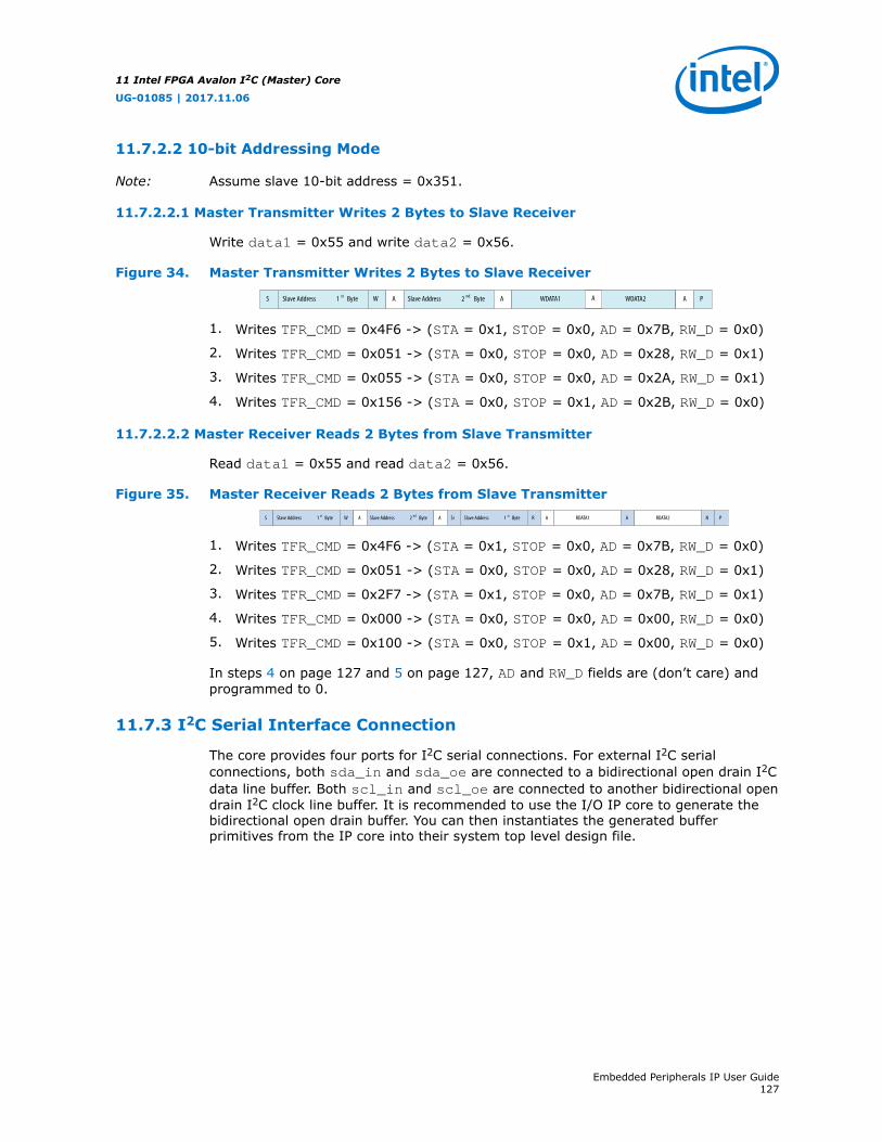
11.7.2.2 10-bit Addressing Mode
Note: Assume slave 10-bit address = 0x351.
11.7.2.2.1 Master Transmitter Writes 2 Bytes to Slave Receiver
Write data1 = 0x55 and write data2 = 0x56.
Figure 34. Master Transmitter Writes 2 Bytes to Slave Receiver
S Slave Address 1 st Byte W A Slave Address 2 nd Byte A WDATA1 WDATA2 AA P
1. Writes TFR_CMD = 0x4F6 -> (STA = 0x1, STOP = 0x0, AD = 0x7B, RW_D = 0x0)
2. Writes TFR_CMD = 0x051 -> (STA = 0x0, STOP = 0x0, AD = 0x28, RW_D = 0x1)
3. Writes TFR_CMD = 0x055 -> (STA = 0x0, STOP = 0x0, AD = 0x2A, RW_D = 0x1)
4. Writes TFR_CMD = 0x156 -> (STA = 0x0, STOP = 0x1, AD = 0x2B, RW_D = 0x0)
11.7.2.2.2 Master Receiver Reads 2 Bytes from Slave Transmitter
Read data1 = 0x55 and read data2 = 0x56.
Figure 35. Master Receiver Reads 2 Bytes from Slave Transmitter
S Slave Address 1 st Byte W A Slave Address 2 nd Byte A Sr Slave Address 1 st Byte R A RDATA1 A RDATA2 N P
1. Writes TFR_CMD = 0x4F6 -> (STA = 0x1, STOP = 0x0, AD = 0x7B, RW_D = 0x0)
2. Writes TFR_CMD = 0x051 -> (STA = 0x0, STOP = 0x0, AD = 0x28, RW_D = 0x1)
3. Writes TFR_CMD = 0x2F7 -> (STA = 0x1, STOP = 0x0, AD = 0x7B, RW_D = 0x1)
4. Writes TFR_CMD = 0x000 -> (STA = 0x0, STOP = 0x0, AD = 0x00, RW_D = 0x0)
5. Writes TFR_CMD = 0x100 -> (STA = 0x0, STOP = 0x1, AD = 0x00, RW_D = 0x0)
In steps 4 on page 127 and 5 on page 127, AD and RW_D fields are (don’t care) andprogrammed to 0.
11.7.3 I2C Serial Interface Connection
The core provides four ports for I2C serial connections. For external I2C serialconnections, both sda_in and sda_oe are connected to a bidirectional open drain I2Cdata line buffer. Both scl_in and scl_oe are connected to another bidirectional opendrain I2C clock line buffer. It is recommended to use the I/O IP core to generate thebidirectional open drain buffer. You can then instantiates the generated bufferprimitives from the IP core into their system top level design file.
11 Intel FPGA Avalon I2C (Master) Core
UG-01085 | 2017.11.06
Embedded Peripherals IP User Guide127

Figure 36. I2C Serial Interface Connection
Vdd
External pull up resistor
Vdd
External pull up resistor
i2c_serial_sda_oe
i2c_serial_sda_in
i2c_serial_scl_oe
i2c_serial_scl_in
1’b0
1’b0
Open drain bidirectional I/O buffer
Open drain bidirectional I/O buffer
I2C data Pad
I2C clock Pad
On chip Off chip
I2C data line
I2C clock line
Sample Code for I2C Serial Interface Connection
Verilog:
assign i2c_serial_scl_in = arduino_adc_scl;assign arduino_adc_scl = i2c_serial_scl_oe ? 1'b0 : 1'bz;
assign i2c_serial_sda_in = arduino_adc_sda;assign arduino_adc_sda = i2c_serial_sda_oe ? 1'b0 : 1'bz;
VHDL:
i2c_scl_in <= arduino_adc_scl; arduino_adc_scl <= '0' when i2c_scl_oe = '1' else 'Z';i2c_sda_in <= arduino_adc_sda; arduino_adc_sda <= '0' when i2c_sda_oe = '1' else 'Z';
11.7.4 Avalon-MM Slave Interface
The Avalon-MM slave interface is configured as follows:
• Bus width: 32-bit
• Burst support: No
• Fixed read & write wait time: 0 cycles
• Fixed read latency: 2 cycles
• Lock support: No
11 Intel FPGA Avalon I2C (Master) Core
UG-01085 | 2017.11.06
Embedded Peripherals IP User Guide128
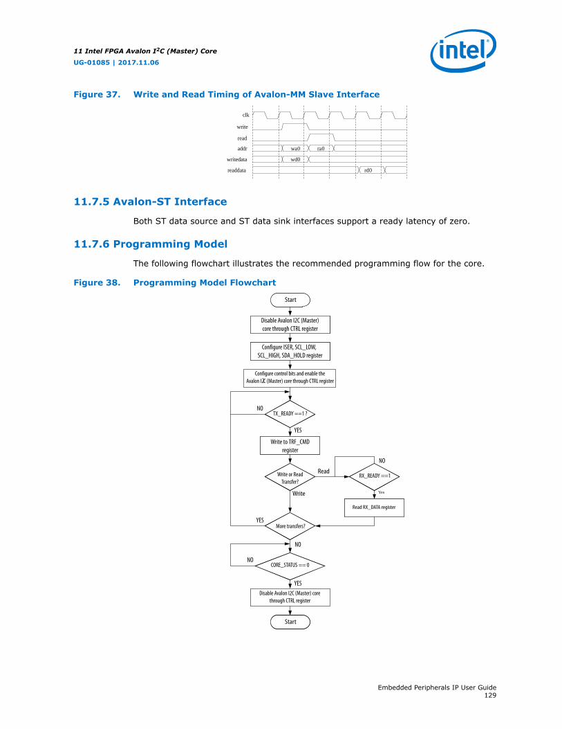
Figure 37. Write and Read Timing of Avalon-MM Slave Interface
clk
write
read
addr
writedata
readdata
wa0 ra0
wd0
rd0
11.7.5 Avalon-ST Interface
Both ST data source and ST data sink interfaces support a ready latency of zero.
11.7.6 Programming Model
The following flowchart illustrates the recommended programming flow for the core.
Figure 38. Programming Model Flowchart
Start
Start
Read RX_DATA register
Read
Write Yes
Disable Avalon I2C (Master) core through CTRL register
Configure ISER, SCL_LOW, SCL_HIGH, SDA_HOLD register
Configure control bits and enable theAvalon I2C (Master) core through CTRL register
NO
YES
NO
YES
NO
NO
YES
TX_READY ==1 ?
RX_READY ==1
More transfers?
Write or ReadTransfer?
CORE_STATUS == 0
Disable Avalon I2C (Master) core through CTRL register
Write to TRF_CMD register
11 Intel FPGA Avalon I2C (Master) Core
UG-01085 | 2017.11.06
Embedded Peripherals IP User Guide129

Note: When either ARBLOST_DET or NACK_DET occur, you need to clear its respectiveinterrupt status register bits in their error handling procedure before continuing with anew I2C transfer. A new I2C transfer can be initiated with or without disabling the core.
Illustration: How to use the API
int main() { ALT_AVALON_I2C_DEV_t *i2c_dev; //pointer to instance structure alt_u8 txbuffer[0x200]; alt_u8 rxbuffer[0x200]; int i; ALT_AVALON_I2C_STATUS_CODE status; //get a pointer to the avalon i2c instance i2c_dev = alt_avalon_i2c_open("/dev/i2c_0"); if (NULL==i2c_dev) { printf("Error: Cannot find /dev/i2c_0\n"); return 1; } //set the address of the device using alt_avalon_i2c_master_target_set(i2c_dev,0x51)
//write data to an eeprom at address 0x0200 txbuffer[0]=2; txbuffer[1]=0; //The eeprom address which will be sent as first two bytes of data for (i=0;i<0x10;i++) txbuffer[i+2]=i; //some data to write status=alt_avalon_i2c_master_tx(i2c_dev,txbuffer, 0x10+2, ALT_AVALON_I2C_NO_INTERRUPTS); if (status!=ALT_AVALON_I2C_SUCCESS) return 1; //FAIL
//read back the data into rxbuffer //This command sends the 2 byte eeprom data address required by the eeprom //Then does a restart and receives the data. status=alt_avalon_i2c_master_tx_rx(i2c_dev, txbuffer, 2, rxbuffer, 0x10, ALT_AVALON_I2C_NO_INTERRUPTS); if (status!=ALT_AVALON_I2C_SUCCESS) return 1; //FAIL return 0;}
//Using the optional irq callback:
int main() { ALT_AVALON_I2C_DEV_t *i2c_dev; //pointer to instance structure alt_u8 txbuffer[0x210]; alt_u8 rxbuffer[0x200]; int i; ALT_AVALON_I2C_STATUS_CODE status;
//storage for the optional provided interrupt handler structure IRQ_DATA_t irq_data; //get a pointer to the avalon i2c instance i2c_dev = alt_avalon_i2c_open("/dev/i2c_0"); if (NULL==i2c_dev) { printf("Error: Cannot find /dev/i2c_0\n"); return 1; }
11 Intel FPGA Avalon I2C (Master) Core
UG-01085 | 2017.11.06
Embedded Peripherals IP User Guide130
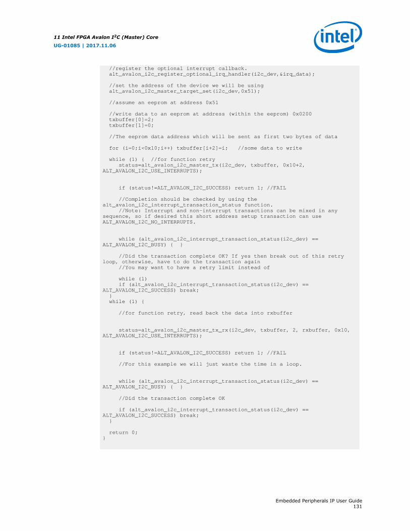
//register the optional interrupt callback. alt_avalon_i2c_register_optional_irq_handler(i2c_dev,&irq_data);
//set the address of the device we will be using alt_avalon_i2c_master_target_set(i2c_dev,0x51);
//assume an eeprom at address 0x51
//write data to an eeprom at address (within the eeprom) 0x0200 txbuffer[0]=2; txbuffer[1]=0; //The eeprom data address which will be sent as first two bytes of data
for (i=0;i<0x10;i++) txbuffer[i+2]=i; //some data to write
while (1) { //for function retry status=alt_avalon_i2c_master_tx(i2c_dev, txbuffer, 0x10+2, ALT_AVALON_I2C_USE_INTERRUPTS); if (status!=ALT_AVALON_I2C_SUCCESS) return 1; //FAIL
//Completion should be checked by using the alt_avalon_i2c_interrupt_transaction_status function. //Note: Interrupt and non-interrupt transactions can be mixed in any sequence, so if desired this short address setup transaction can use ALT_AVALON_I2C_NO_INTERRUPTS. while (alt_avalon_i2c_interrupt_transaction_status(i2c_dev) == ALT_AVALON_I2C_BUSY) { } //Did the transaction complete OK? If yes then break out of this retry loop, otherwise, have to do the transaction again //You may want to have a retry limit instead of while (1) if (alt_avalon_i2c_interrupt_transaction_status(i2c_dev) == ALT_AVALON_I2C_SUCCESS) break; } while (1) { //for function retry, read back the data into rxbuffer status=alt_avalon_i2c_master_tx_rx(i2c_dev, txbuffer, 2, rxbuffer, 0x10, ALT_AVALON_I2C_USE_INTERRUPTS); if (status!=ALT_AVALON_I2C_SUCCESS) return 1; //FAIL //For this example we will just waste the time in a loop. while (alt_avalon_i2c_interrupt_transaction_status(i2c_dev) == ALT_AVALON_I2C_BUSY) { } //Did the transaction complete OK if (alt_avalon_i2c_interrupt_transaction_status(i2c_dev) == ALT_AVALON_I2C_SUCCESS) break; } return 0;}
11 Intel FPGA Avalon I2C (Master) Core
UG-01085 | 2017.11.06
Embedded Peripherals IP User Guide131

11.8 Document Revision History
Table 101. Intel FPGA Avalon I2C (Master) Core Revision History
Date Version Changes
November 2017 2017.11.06 • Added the sample verilog code for I2C Serial Interface Connection.• Added the illustration for using API in Programming Model.
October 2016 2016.10.28 Initial release
11 Intel FPGA Avalon I2C (Master) Core
UG-01085 | 2017.11.06
Embedded Peripherals IP User Guide132
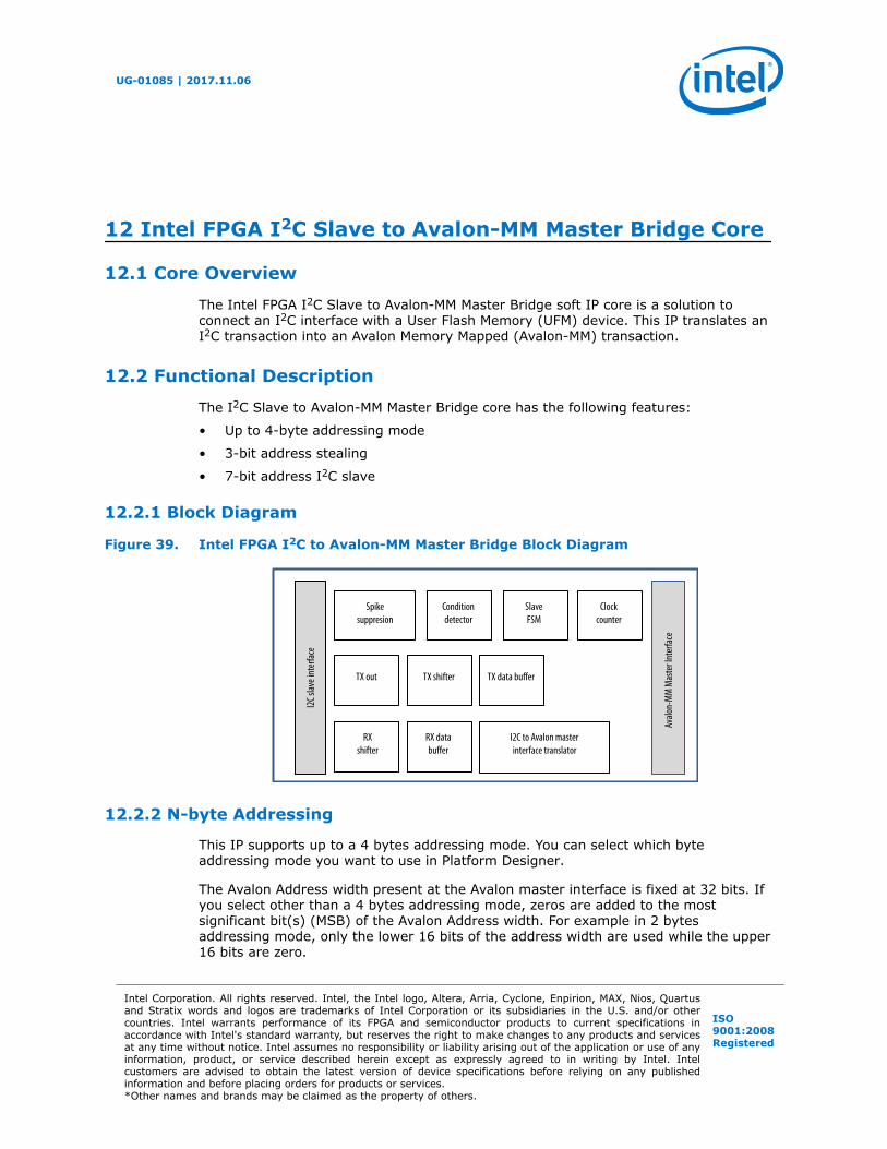
12 Intel FPGA I2C Slave to Avalon-MM Master Bridge Core
12.1 Core Overview
The Intel FPGA I2C Slave to Avalon-MM Master Bridge soft IP core is a solution toconnect an I2C interface with a User Flash Memory (UFM) device. This IP translates anI2C transaction into an Avalon Memory Mapped (Avalon-MM) transaction.
12.2 Functional Description
The I2C Slave to Avalon-MM Master Bridge core has the following features:
• Up to 4-byte addressing mode
• 3-bit address stealing
• 7-bit address I2C slave
12.2.1 Block Diagram
Figure 39. Intel FPGA I2C to Avalon-MM Master Bridge Block Diagram
Avalo
n-M
M M
aste
r Int
erfac
e
I2C sl
ave i
nter
face
Conditiondetector
SlaveFSM
Clockcounter
Spikesuppresion
TX out TX shifter TX data buffer
RXshifter
RX databuffer
I2C to Avalon masterinterface translator
12.2.2 N-byte Addressing
This IP supports up to a 4 bytes addressing mode. You can select which byteaddressing mode you want to use in Platform Designer.
The Avalon Address width present at the Avalon master interface is fixed at 32 bits. Ifyou select other than a 4 bytes addressing mode, zeros are added to the mostsignificant bit(s) (MSB) of the Avalon Address width. For example in 2 bytesaddressing mode, only the lower 16 bits of the address width are used while the upper16 bits are zero.
UG-01085 | 2017.11.06
Intel Corporation. All rights reserved. Intel, the Intel logo, Altera, Arria, Cyclone, Enpirion, MAX, Nios, Quartusand Stratix words and logos are trademarks of Intel Corporation or its subsidiaries in the U.S. and/or othercountries. Intel warrants performance of its FPGA and semiconductor products to current specifications inaccordance with Intel's standard warranty, but reserves the right to make changes to any products and servicesat any time without notice. Intel assumes no responsibility or liability arising out of the application or use of anyinformation, product, or service described herein except as expressly agreed to in writing by Intel. Intelcustomers are advised to obtain the latest version of device specifications before relying on any publishedinformation and before placing orders for products or services.*Other names and brands may be claimed as the property of others.
ISO9001:2008Registered
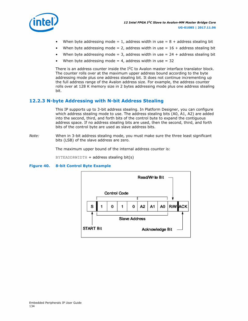
• When byte addressing mode = 1, address width in use = 8 + address stealing bit
• When byte addressing mode = 2, address width in use = 16 + address stealing bit
• When byte addressing mode = 3, address width in use = 24 + address stealing bit
• When byte addressing mode = 4, address width in use = 32
There is an address counter inside the I2C to Avalon master interface translator block.The counter rolls over at the maximum upper address bound according to the byteaddressing mode plus one address stealing bit. It does not continue incrementing upthe full address range of the Avalon address size. For example, the address counterrolls over at 128 K memory size in 2 bytes addressing mode plus one address stealingbit.
12.2.3 N-byte Addressing with N-bit Address Stealing
This IP supports up to 3-bit address stealing. In Platform Designer, you can configurewhich address stealing mode to use. The address stealing bits (A0, A1, A2) are addedinto the second, third, and forth bits of the control byte to expand the contiguousaddress space. If no address stealing bits are used, then the second, third, and forthbits of the control byte are used as slave address bits.
Note: When in 3-bit address stealing mode, you must make sure the three least significantbits (LSB) of the slave address are zero.
The maximum upper bound of the internal address counter is:
BYTEADDRWIDTH + address stealing bit(s)
Figure 40. 8-bit Control Byte Example
12 Intel FPGA I2C Slave to Avalon-MM Master Bridge Core
UG-01085 | 2017.11.06
Embedded Peripherals IP User Guide134

12.2.4 Read Operation
The Avalon read data width is 32 bits wide. A 32-bit width limits the bridge to onlyissue word align Avalon addresses. It also allows the upstream I2C master to read anysequence of bytes on any address alignment. The conversion logic which sits betweenthe Avalon interface and I2C interface, translates the address alignment and returnsthe correct 8-bit data to the I2C master from the 32-bit Avalon read data.
Read Operation conversion logic flow:
• Checks the address alignment issued by the I2C master (first byte, second byte,third byte or forth byte).
• Issues a word align Avalon address according to the address sent by the I2Cmaster with the two LSBs zero.
• Returns read data to the I2C master according to the address alignment.
This IP supports three types of read operations:
• Random address read
• Current address read
• Sequential read
Upon receiving of the slave address with the R/W bit set to one, the bridge issues anacknowledge to the I2C master. The bridge keeps the Avalon read signal high for oneclock cycle with the Avalon wait request signal low, then receives an 8-bit Avalon readdata word and upstreams the read data to the I2C master.
12.2.4.1 Random Address Read
Random read operations allow the upstream I2C master to access any memorylocation in a random manner. To perform this type of read operation, you must firstset the byte address. The I2C master issues a byte address to the bridge as part of awrite operation then followed by a read command. After the read command is issued,the internal address counter points to the address location following the one that wasjust read. The upper address bits are transferred first, followed by the LSB(s).
Figure 41. Random Address Read
12.2.4.2 Sequential Address Read
Sequential reads are initiated in the same way as a random read except after thebridge has received the first data byte, the upstream I2C master issues anacknowledge as opposed to a Stop condition. This directs the bridge to keep theAvalon read signal high for the next sequential address. The internal address counterincrements by one at the completion of each read operation and allows the entirememory contents to be serially read during one operation.
12 Intel FPGA I2C Slave to Avalon-MM Master Bridge Core
UG-01085 | 2017.11.06
Embedded Peripherals IP User Guide135
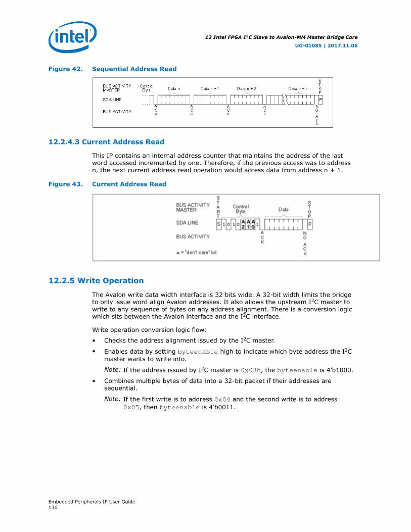
Figure 42. Sequential Address Read
12.2.4.3 Current Address Read
This IP contains an internal address counter that maintains the address of the lastword accessed incremented by one. Therefore, if the previous access was to addressn, the next current address read operation would access data from address n + 1.
Figure 43. Current Address Read
12.2.5 Write Operation
The Avalon write data width interface is 32 bits wide. A 32-bit width limits the bridgeto only issue word align Avalon addresses. It also allows the upstream I2C master towrite to any sequence of bytes on any address alignment. There is a conversion logicwhich sits between the Avalon interface and the I2C interface.
Write operation conversion logic flow:
• Checks the address alignment issued by the I2C master.
• Enables data by setting byteenable high to indicate which byte address the I2Cmaster wants to write into.
Note: If the address issued by I2C master is 0x03h, the byteenable is 4’b1000.
• Combines multiple bytes of data into a 32-bit packet if their addresses aresequential.
Note: If the first write is to address 0x04 and the second write is to address0x05, then byteenable is 4’b0011.
12 Intel FPGA I2C Slave to Avalon-MM Master Bridge Core
UG-01085 | 2017.11.06
Embedded Peripherals IP User Guide136

Legal byteenable combinations are 4’b0001, 4’b0010, 4’b0100, 4’b1000, 4’b0011,4’b1100 and 4’b1111.
• If the write request issued by the I2C master ends up with an illegal byteenablecombination such as, 4’b0110, 4’b0111, or 4’b1110, then the bridge generatesmultiple Avalon byte writes.
Note: If the sequential write request from the I2C master starts from 0x0 andends at 0x02 (illegal byteenable, b’0111), then the bridge will generatethree Avalon write requests with legal byteenable 4’b0001, 4’b0010 and4’b0100.
• Issues a word align Avalon address according to the address sent by the I2Cmaster with the two LSB set to zero.
Upon receiving of the slave address with the R/W bit set to zero, the bridge issues anacknowledge to the I2C master. The next byte transmitted by the master is the byteaddress. The byte address is written into the address counter inside the bridge. Thebridge acknowledges the I2C master again and the master transmits the data byte tobe written into the addressed memory location. The master keeps sending data bytesto the bridge and terminates the operation with a Stop condition at the end.
Figure 44. Write Operation
12 Intel FPGA I2C Slave to Avalon-MM Master Bridge Core
UG-01085 | 2017.11.06
Embedded Peripherals IP User Guide137

12.2.6 Interacting with Multi-Master
This IP core is able to integrate multiple I2C masters provided the I2C masters supportthe arbitration feature. The masters which support arbitration always compares thedata value it drives into the bus with the actual value observed on the bus. If bothsets of data do not match, then the master loses arbitration. The I2C slave core in thebridge does not observe the bus.
For example, let’s say Master 1 is writing to the bridge while Master 2 is performing aread. Master 1 will win the arbitration during the R/W bit because Master 1 is pullingdown the bus, while Master 2 is driving high to the bus. The effective value of the busduring the R/W bit cycle is zero. In this case, Master 2 knows it loses the arbitrationbecause it observes a different value on the bus than what is being driven.
If both masters are performing a write, then the arbitration process checks thedifferent data value driven by both masters to determine which one wins thearbitration.
If both masters are performing a read, then no one loses the arbitration since thesingle slave is driving the bus to both masters (no collision).
12 Intel FPGA I2C Slave to Avalon-MM Master Bridge Core
UG-01085 | 2017.11.06
Embedded Peripherals IP User Guide138

12.3 Platform Designer Parameters
Figure 45. Intel FPGA I2C Slave to Avalon MM Master Bridge Qys Interface
Table 102. Platform Designer Parameters
Parameter Legal Values DefaultValues
Description
I2C Slave Address 0:127 127 This parameter represents the target address of the I2Cslave which sits in the bridge.
Byte Addressing mode 1, 2, 3, 4 2 This parameter allows you to select the number of addressbytes you want to configure according to the flash capacityused.• 1=8 address bit• 2=16 address bit• 3=24 address bit• 4=32 address bit
Number of Address Stealingbit
0, 1, 2, 3 0 This parameter allows you to select the number of addressstealing bits to expand the contiguous address space.
Enable Read only mode ON, OFF OFF Enables read only support where the write operation isremoved to improve resource count.
12.4 Signals
Table 103. Intel FPGA I2C Slave to Avalon-MM Master Bridge Signals
Signal Width Direction Description
Avalon-MM interface
clk 1 Input Clock signal
rst_n 1 Input Reset signal
continued...
12 Intel FPGA I2C Slave to Avalon-MM Master Bridge Core
UG-01085 | 2017.11.06
Embedded Peripherals IP User Guide139
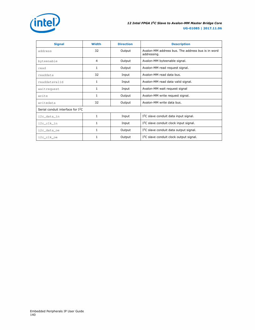
Signal Width Direction Description
address 32 Output Avalon-MM address bus. The address bus is in wordaddressing.
byteenable 4 Output Avalon-MM byteenable signal.
read 1 Output Avalon-MM read request signal.
readdata 32 Input Avalon-MM read data bus.
readdatavalid 1 Input Avalon-MM read data valid signal.
waitrequest 1 Input Avalon-MM wait request signal
write 1 Output Avalon-MM write request signal.
writedata 32 Output Avalon-MM write data bus.
Serial conduit interface for I2C
i2c_data_in 1 Input I2C slave conduit data input signal.
i2c_clk_in 1 Input I2C slave conduit clock input signal.
i2c_data_oe 1 Output I2C slave conduit data output signal.
i2c_clk_oe 1 Output I2C slave conduit clock output signal.
12 Intel FPGA I2C Slave to Avalon-MM Master Bridge Core
UG-01085 | 2017.11.06
Embedded Peripherals IP User Guide140
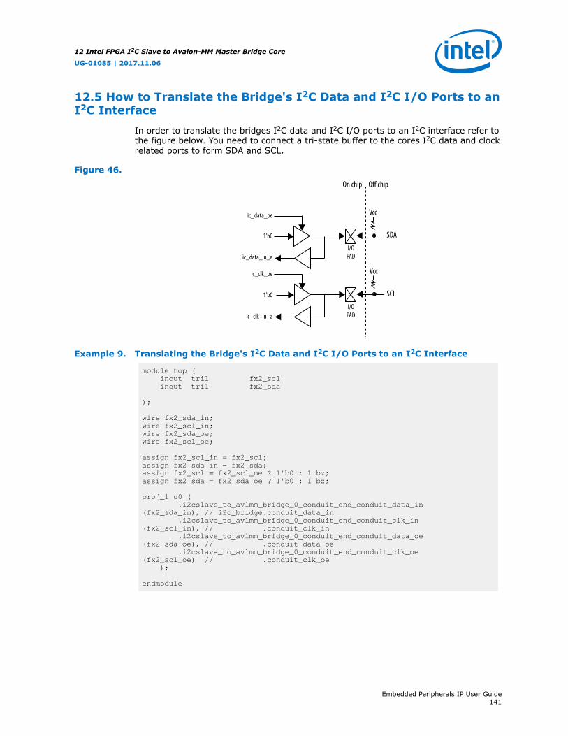
12.5 How to Translate the Bridge's I2C Data and I2C I/O Ports to anI2C Interface
In order to translate the bridges I2C data and I2C I/O ports to an I2C interface refer tothe figure below. You need to connect a tri-state buffer to the cores I2C data and clockrelated ports to form SDA and SCL.
Figure 46.On chip Off chip
SDA
SCL
Vcc
Vcc
I/OPAD
I/OPAD
ic_data_oe
ic_clk_oe
1’b0
1’b0
ic_data_in_a
ic_clk_in_a
Example 9. Translating the Bridge's I2C Data and I2C I/O Ports to an I2C Interface
module top ( inout tri1 fx2_scl, inout tri1 fx2_sda
);
wire fx2_sda_in;wire fx2_scl_in;wire fx2_sda_oe;wire fx2_scl_oe;
assign fx2_scl_in = fx2_scl;assign fx2_sda_in = fx2_sda;assign fx2_scl = fx2_scl_oe ? 1'b0 : 1'bz;assign fx2_sda = fx2_sda_oe ? 1'b0 : 1'bz;
proj_1 u0 ( .i2cslave_to_avlmm_bridge_0_conduit_end_conduit_data_in (fx2_sda_in), // i2c_bridge.conduit_data_in .i2cslave_to_avlmm_bridge_0_conduit_end_conduit_clk_in (fx2_scl_in), // .conduit_clk_in .i2cslave_to_avlmm_bridge_0_conduit_end_conduit_data_oe (fx2_sda_oe), // .conduit_data_oe .i2cslave_to_avlmm_bridge_0_conduit_end_conduit_clk_oe (fx2_scl_oe) // .conduit_clk_oe );
endmodule
12 Intel FPGA I2C Slave to Avalon-MM Master Bridge Core
UG-01085 | 2017.11.06
Embedded Peripherals IP User Guide141
12.6 Document Revision History
Table 104. Altera I2C Slave to Avalon-MM Master Bridge Core Revision History
Date Version Changes
Ocotober 2016 2016.10.28 Updates:• Table 103 on page 139
— address direction updated— waitrequest added
June 2016 2016.06.17 New topic:• How to Translate the Bridge's I2C Data and I2C I/O Ports to an I2C
Interface on page 141
May 2016 2016.05.03 Initial release.
12 Intel FPGA I2C Slave to Avalon-MM Master Bridge Core
UG-01085 | 2017.11.06
Embedded Peripherals IP User Guide142

13 Compact Flash Core
13.1 Core Overview
The CompactFlash core allows you to connect systems built on Osys to CompactFlashstorage cards in true IDE mode by providing an Avalon Memory-Mapped (Avalon-MM)interface to the registers on the storage cards. The core supports PIO mode 0.
The CompactFlash core also provides an Avalon-MM slave interface which can be usedby Avalon-MM master peripherals such as a Nios II processor to communicate with theCompactFlash core and manage its operations.
13.2 Functional Description
Figure 47. System With a CompactFlash Core
FPGA
edi
ctl
data
address
cfctl
idectl
Registers
IRQ
data
address
IRQ
Compact FlashDevice
Avalon-to-Compact Flash
Avalo
n-M
M Sl
ave P
ort
Avalo
n-M
M Sl
ave P
ort
Syste
m In
terco
nnec
t Fab
ric
Avalon-MMMaster
(e.g. CPU)
As shown in the block diagram, the CompactFlash core provides two Avalon-MM slaveinterfaces: the ide slave port for accessing the registers on the CompactFlash deviceand the ctl slave port for accessing the core's internal registers. These registers canbe used by Avalon-MM master peripherals such as a Nios II processor to control theoperations of the CompactFlash core and to transfer data to and from theCompactFlash device.
You can set the CompactFlash core to generate two active-high interrupt requests(IRQs): one signals the insertion and removal of a CompactFlash device and the otherpasses interrupt signals from the CompactFlash device.
UG-01085 | 2017.11.06
Intel Corporation. All rights reserved. Intel, the Intel logo, Altera, Arria, Cyclone, Enpirion, MAX, Nios, Quartusand Stratix words and logos are trademarks of Intel Corporation or its subsidiaries in the U.S. and/or othercountries. Intel warrants performance of its FPGA and semiconductor products to current specifications inaccordance with Intel's standard warranty, but reserves the right to make changes to any products and servicesat any time without notice. Intel assumes no responsibility or liability arising out of the application or use of anyinformation, product, or service described herein except as expressly agreed to in writing by Intel. Intelcustomers are advised to obtain the latest version of device specifications before relying on any publishedinformation and before placing orders for products or services.*Other names and brands may be claimed as the property of others.
ISO9001:2008Registered

The CompactFlash core maps the Avalon-MM bus signals to the CompactFlash devicewith proper timing, thus allowing Avalon-MM master peripherals to directly access theregisters on the CompactFlash device.
For more information, refer to the CF+ and CompactFlash specifications available atwww.compact-flash.org.
13.3 Required Connections
The table below lists the required connections between the CompactFlash core and theCompactFlash device.
Table 105. Core to Device Required Connections
CompactFlash Interface SignalName
Pin Type CompactFlash Pin Number
addr[0] Output 20
addr[1] Output 19
addr[2] Output 18
addr[3] Output 17
addr[4] Output 16
addr[5] Output 15
addr[6] Output 14
addr[7] Output 12
addr[8] Output 11
addr[9] Output 10
addr[10] Output 8
atasel_n Output 9
cs_n[0] Output 7
cs_n[1] Output 32
data[0] Input/Output 21
data[1] Input/Output 22
data[2] Input/Output 23
data[3] Input/Output 2
data[4] Input/Output 3
data[5] Input/Output 4
data[6] Input/Output 5
data[7] Input/Output 6
data[8] Input/Output 47
data[9] Input/Output 48
data[10] Input/Output 49
continued...
13 Compact Flash Core
UG-01085 | 2017.11.06
Embedded Peripherals IP User Guide144

CompactFlash Interface SignalName
Pin Type CompactFlash Pin Number
data[11] Input/Output 27
data[12] Input/Output 28
data[13] Input/Output 29
data[14] Input/Output 30
data[15] Input/Output 31
detect Input 25 or 26
intrq Input 37
iord_n Output 34
iordy Input 42
iowr_n Output 35
power Output CompactFlash power controller, ifpresent
reset_n Output 41
rfu Output 44
we_n Output 46
13.4 Software Programming Model
This section describes the software programming model for the CompactFlash core.
13.4.1 HAL System Library Support
The Intel-provided HAL API functions include a device driver that you can use toinitialize the CompactFlash core. To perform other operations, use the low-levelmacros provided.
For more information on the macros, refer to the "Software Files" section.
Related Links
Software Files on page 145
13.4.2 Software Files
The CompactFlash core provides the following software files. These files define thelow-level access to the hardware. Application developers should not modify these files.
• altera_avalon_cf_regs.h—The header file that defines the core's registermaps.
• altera_avalon_cf.h, altera_avalon_cf.c—The header and source codefor the functions and variables required to integrate the driver into the HAL systemlibrary.
13 Compact Flash Core
UG-01085 | 2017.11.06
Embedded Peripherals IP User Guide145
13.4.3 Register Maps
This section describes the register maps for the Avalon-MM slave interfaces.
13.4.3.1 Ide Registers
The ide port in the CompactFlash core allows you to access the IDE registers on aCompactFlash device.
Table 106. Ide Register Map
Offset Register Names
Read Operation Write Operation
0 RD Data WR Data
1 Error Features
2 Sector Count Sector Count
3 Sector No Sector No
4 Cylinder Low Cylinder Low
5 Cylinder High Cylinder High
6 Select Card/Head Select Card/Head
7 Status Command
14 Alt Status Device Control
13.4.3.2 Ctl Registers
The ctl port in the CompactFlash core provides access to the registers which controlthe core’s operation and interface.
Table 107. Ctl Register Map
Offset Register Fields
31:4 3 2 1 0
0 cfctl Reserved IDET RST PWR DET
1 idectl Reserved IIDE
2 Reserved Reserved
3 Reserved Reserved
13.4.3.3 Cfctl Register
The cfctl register controls the operations of the CompactFlash core. Reading the cfctlregister clears the interrupt.
13 Compact Flash Core
UG-01085 | 2017.11.06
Embedded Peripherals IP User Guide146

Table 108. cfctl Register Bits
Bit Number Bit Name Read/Write Description
0 DET RO Detect. This bit is set to 1 when the core detects a CompactFlashdevice.
1 PWR RW Power. When this bit is set to 1, power is being supplied to theCompactFlash device.
2 RST RW Reset. When this bit is set to 1, the CompactFlash device is held in areset state. Setting this bit to 0 returns the device to its active state.
3 IDET RW Detect Interrupt Enable. When this bit is set to 1, the CompactFlashcore generates an interrupt each time the value of the det bitchanges.
13.4.3.4 idectl Register
The idectl register controls the interface to the CompactFlash device.
Table 109. idectl Register
Bit Number Bit Name Read/Write Description
0 IIDE RW IDE Interrupt Enable. When this bit is set to 1, the CompactFlash coregenerates an interrupt following an interrupt generated by theCompactFlash device. Setting this bit to 0 disables the IDE interrupt.
13.5 Document Revision History
Table 110. Compact Flash Core Revision History
Date Version Changes
July 2014 2014.07.24 Removed mention of SOPC Builder, updated to Platform Designer
December 2010 v10.1.0 Removed the “Device Support”, “Instantiating the Core in SOPC Builder”,and “Referenced Documents” sections.
July 2010 v10.0.0 No change from previous release.
November 2009 v9.1.0 No change from previous release.
March 2009 v9.0.0 No change from previous release.
November 2008 v8.1.0 Changed to 8-1/2 x 11 page size. No change to content.
May 2008 v8.0.0 Added the mode supported by the CompactFlash core.
For previous versions of this chapter, refer to the Intel Quartus Prime HandbookArchive.
13 Compact Flash Core
UG-01085 | 2017.11.06
Embedded Peripherals IP User Guide147
14 EPCS Serial Flash Controller Core
14.1 Core Overview
The EPCS serial flash controller core with Avalon interface allows Nios II systems toaccess an Intel EPCS serial configuration device. Intel provides drivers that integrateinto the Nios II hardware abstraction layer (HAL) system library, allowing you to readand write the EPCS device using the familiar HAL application program interface (API)for flash devices.
Using the EPCS serial flash controller core, Nios II systems can:
• Store program code in the EPCS device. The EPCS serial flash controller coreprovides a boot-loader feature that allows Nios II systems to store the mainprogram code in an EPCS device.
• Store non-volatile program data, such as a serial number, a NIC number, andother persistent data.
• Manage the device configuration data. For example, a network-enabled embeddedsystem can receive new FPGA configuration data over a network, and use the coreto program the new data into an EPCS serial configuration device.
The EPCS serial flash controller core is Platform Designer-ready and integrateseasily into any Platform Designer-generated system. The flash programmer utilityin the Nios II IDE allows you to manage and program data contents into the EPCSdevice.
For information about the EPCS serial configuration device family, refer to theSerial Configuration Devices Data Sheet.
For details about using the Nios II HAL API to read and write flash memory, referto the Nios II Software Developer's Handbook.
For details about managing and programming the EPCS memory contents, refer tothe Nios II Flash Programmer User Guide.
For Nios II processor users, the EPCS serial flash controller core supersedes theActive Serial Memory Interface (ASMI) device. New designs should use the EPCSserial flash controller core instead of the ASMI core.
Related Links
• Serial Configuration Devices (EPCS1, EPCS4, EPCS16, EPCS64 and EPCS128) DataSheet
• Nios II Classic Software Developer's Handbook
• Nios II Flash Programmer User Guide
UG-01085 | 2017.11.06
Intel Corporation. All rights reserved. Intel, the Intel logo, Altera, Arria, Cyclone, Enpirion, MAX, Nios, Quartusand Stratix words and logos are trademarks of Intel Corporation or its subsidiaries in the U.S. and/or othercountries. Intel warrants performance of its FPGA and semiconductor products to current specifications inaccordance with Intel's standard warranty, but reserves the right to make changes to any products and servicesat any time without notice. Intel assumes no responsibility or liability arising out of the application or use of anyinformation, product, or service described herein except as expressly agreed to in writing by Intel. Intelcustomers are advised to obtain the latest version of device specifications before relying on any publishedinformation and before placing orders for products or services.*Other names and brands may be claimed as the property of others.
ISO9001:2008Registered

14.2 Functional Description
As shown below, the EPCS device's memory can be thought of as two separateregions:
• FPGA configuration memory—FPGA configuration data is stored in this region.
• General-purpose memory—If the FPGA configuration data does not fill up theentire EPCS device, any left-over space can be used for general-purpose data andsystem startup code.
Figure 48. Nios II System Integrating an EPCS Serial Flash Controller Core
FPGA
EPCS Serial Configuration
Device
OtherOn-Chip
Peripheral(s)
Nios II CPU
EPCSController CoreConfig
Memory
General-PurposeMemory
Boot-LoaderROM
Syste
m In
terco
nnec
t Fab
ric
• By virtue of the HAL generic device model for flash devices, accessing the EPCSdevice using the HAL API is the same as accessing any flash memory. The EPCSdevice has a special-purpose hardware interface, so Nios II programs must readand write the EPCS memory using the provided HAL flash drivers.
The EPCS serial flash controller core contains an on-chip memory for storing a boot-loader program. When used in conjunction with Cyclone and Cyclone II devices, thecore requires 512 bytes of boot-loader ROM. For Cyclone III, Cyclone IV, Intel Cyclone10 LP, Stratix II, and newer device families in the Stratix series, the core requires1 KByte of boot-loader ROM. The Nios II processor can be configured to boot from theEPCS serial flash controller core. To do so, set the Nios II reset address to the baseaddress of the EPCS serial flash controller core. In this case, after reset the CPU firstexecutes code from the boot-loader ROM, which copies data from the EPCS general-purpose memory region into a RAM. Then, program control transfers to the RAM. TheNios II IDE provides facilities to compile a program for storage in the EPCS device, andcreate a programming file to program into the EPCS device.
For more information, refer to the Nios II Flash Programmer User Guide.
14 EPCS Serial Flash Controller Core
UG-01085 | 2017.11.06
Embedded Peripherals IP User Guide149

If you program the EPCS device using the Intel Quartus Prime Programmer, allprevious content is erased. To program the EPCS device with a combination of FPGAconfiguration data and Nios II program data, use the Nios II IDE flash programmerutility.
The Intel EPCS configuration device connects to the FPGA through dedicated pins onthe FPGA, not through general-purpose I/O pins. In all Intel device families exceptCyclone III, Cyclone IV, and Intel Cyclone 10 LP the EPCS serial flash controller coredoes not create any I/O ports on the top-level Platform Designer system module. Ifthe EPCS device and the FPGA are wired together on a board for configuration usingthe EPCS device (in other words, active serial configuration mode), no furtherconnection is necessary between the EPCS serial flash controller core and the EPCSdevice. When you compile the Platform Designer system in the Intel Quartus Primesoftware, the EPCS serial flash controller core signals are routed automatically to thedevice pins for the EPCS device.
You, however, have the option not to use the dedicated pins on the FPGA (active serialconfiguration mode) by turning off the respective parameters in the MegaWizardinterface. When this option is turned off or when the target device is a Cyclone III,Cyclone IV device, or Intel Cyclone 10 LP you have the flexibility to connect the outputpins, which are exported to the top-level design, to any EPCS devices. Perform thefollowing tasks in the Intel Quartus Prime software to make the necessary pinassignments:
• On the Dual-purpose pins page (Assignments > Devices > Device and PinOptions), ensure that the following pins are assigned to the respective values:
— Data[0] = Use as regular I/O
— Data[1] = Use as regularr I/O
— DCLK = Use as regular I/O
— FLASH_nCE/nCS0 = Use as regular I/O
• Using the Pin Planner (Assignments > Pins), ensure that the following pins areassigned to the respective configuration functions on the device:
— data0_to_the_epcs_controller = DATA0
— sdo_from the_epcs_controller = DATA1,ASDO
— dclk_from_epcs_controller = DCLK
— sce_from_the_epcs_controller = FLASH_nCE
For more information about the configuration pins in Intel devices, refer to the Pin-OutFiles for Intel Devices page.
Related Links
• Nios II Flash Programmer User Guide
• Pin-Out Files for Intel FPGA devices
14.2.1 Avalon-MM Slave Interface and Registers
The EPCS serial flash controller core has a single Avalon-MM slave interface thatprovides access to both boot-loader code and registers that control the core. As shownin below, the first segment is dedicated to the boot-loader code, and the next seven
14 EPCS Serial Flash Controller Core
UG-01085 | 2017.11.06
Embedded Peripherals IP User Guide150
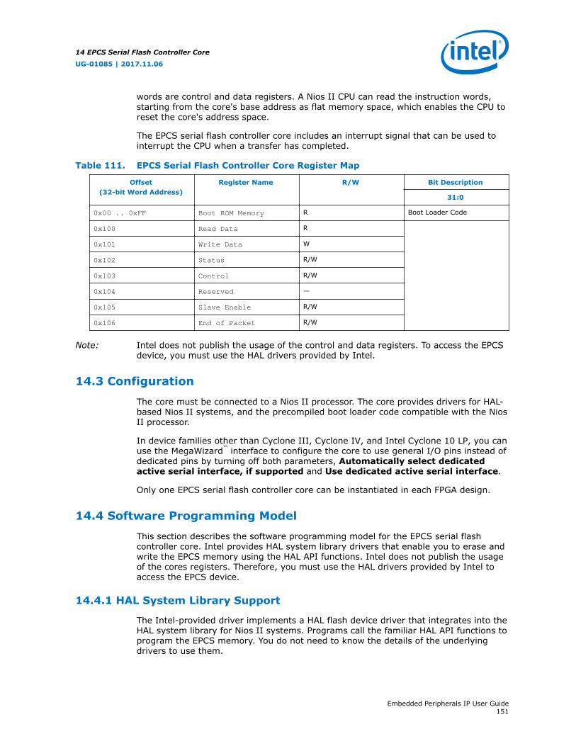
words are control and data registers. A Nios II CPU can read the instruction words,starting from the core's base address as flat memory space, which enables the CPU toreset the core's address space.
The EPCS serial flash controller core includes an interrupt signal that can be used tointerrupt the CPU when a transfer has completed.
Table 111. EPCS Serial Flash Controller Core Register Map
Offset(32-bit Word Address)
Register Name R/W Bit Description
31:0
0x00 .. 0xFF Boot ROM Memory R Boot Loader Code
0x100 Read Data R
0x101 Write Data W
0x102 Status R/W
0x103 Control R/W
0x104 Reserved —
0x105 Slave Enable R/W
0x106 End of Packet R/W
Note: Intel does not publish the usage of the control and data registers. To access the EPCSdevice, you must use the HAL drivers provided by Intel.
14.3 Configuration
The core must be connected to a Nios II processor. The core provides drivers for HAL-based Nios II systems, and the precompiled boot loader code compatible with the NiosII processor.
In device families other than Cyclone III, Cyclone IV, and Intel Cyclone 10 LP, you canuse the MegaWizard™ interface to configure the core to use general I/O pins instead ofdedicated pins by turning off both parameters, Automatically select dedicatedactive serial interface, if supported and Use dedicated active serial interface.
Only one EPCS serial flash controller core can be instantiated in each FPGA design.
14.4 Software Programming Model
This section describes the software programming model for the EPCS serial flashcontroller core. Intel provides HAL system library drivers that enable you to erase andwrite the EPCS memory using the HAL API functions. Intel does not publish the usageof the cores registers. Therefore, you must use the HAL drivers provided by Intel toaccess the EPCS device.
14.4.1 HAL System Library Support
The Intel-provided driver implements a HAL flash device driver that integrates into theHAL system library for Nios II systems. Programs call the familiar HAL API functions toprogram the EPCS memory. You do not need to know the details of the underlyingdrivers to use them.
14 EPCS Serial Flash Controller Core
UG-01085 | 2017.11.06
Embedded Peripherals IP User Guide151

The driver for the EPCS device is excluded when the reduced device drivers option isenabled in a BSP or system library. To force inclusion of the EPCS drivers in a BSP withthe reduced device drivers option enabled, you can define the preprocessor symbol,ALT_USE_EPCS_FLASH, before including the header, as follows:
#define ALT_USE_EPCS_FLASH
#include <altera_avalon_epcs_flash_controller.h>
The HAL API for programming flash, including C-code examples, is described in detailin the Nios II Classic Software Developer's Handbook.
For details about managing and programming the EPCS device contents, refer to the Nios II Flash Programmer User Guide.
14.4.2 Software Files
The EPCS serial flash controller core provides the following software files. These filesprovide low-level access to the hardware and drivers that integrate into the Nios IIHAL system library. Application developers should not modify these files.
• altera_avalon_epcs_flash_controller.h,altera_avalon_epcs_flash_controller.c—Header and source files thatdefine the drivers required for integration into the HAL system library.
• epcs_commands.h, epcs_commands.c—Header and source files that directlycontrol the EPCS device hardware to read and write the device. These files alsorely on theIntel FPGA SPI core drivers.
14.5 Document Revision History
Table 112. EPCS Serial Flash Controller Core Revision History
Date Version Changes
July 2014 2014.07.24 Removed mention of SOPC Builder, updated to Platform Designer
December 2013 v13.1.0 Removed Cyclone and Cyclone II device information in the "EPCS SerialFlash Controller Core Register Map" table.
December 2010 v10.1.0 Removed the “Device Support”, “Instantiating the Core in SOPC Builder”,and “Referenced Documents” sections.
July 2010 v10.0.0 No change from previous release.
November 2009 v9.1.0 Revised descriptions of register fields and bits.Updated the section on HAL System Library Support.
March 2009 v9.0.0 Updated the boot ROM memory offset for other device familes in the EPCSSerial Flash Controller Core Register Map" table.
November 2008 v8.1.0 Changed to 8-1/2 x 11 page size. No change to content.
May 2008 v8.0.0 Updated the boot rom size.Added additional steps to perform to connect output pins in Cyclone IIIdevices.
For previous versions of this chapter, refer to the Intel Quartus Prime HandbookArchive.
14 EPCS Serial Flash Controller Core
UG-01085 | 2017.11.06
Embedded Peripherals IP User Guide152
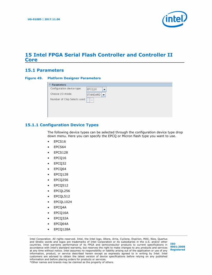
15 Intel FPGA Serial Flash Controller and Controller IICore
15.1 Parameters
Figure 49. Platform Designer Parameters
15.1.1 Configuration Device Types
The following device types can be selected through the configuration device type dropdown menu. Here you can specify the EPCQ or Micron flash type you want to use.
• EPCS16
• EPCS64
• EPCS128
• EPCQ16
• EPCQ32
• EPCQ64
• EPCQ128
• EPCQ256
• EPCQ512
• EPCQL256
• EPCQL512
• EPCQL1024
• EPCQ4A
• EPCQ16A
• EPCQ32A
• EPCQ64A
• EPCQ128A
UG-01085 | 2017.11.06
Intel Corporation. All rights reserved. Intel, the Intel logo, Altera, Arria, Cyclone, Enpirion, MAX, Nios, Quartusand Stratix words and logos are trademarks of Intel Corporation or its subsidiaries in the U.S. and/or othercountries. Intel warrants performance of its FPGA and semiconductor products to current specifications inaccordance with Intel's standard warranty, but reserves the right to make changes to any products and servicesat any time without notice. Intel assumes no responsibility or liability arising out of the application or use of anyinformation, product, or service described herein except as expressly agreed to in writing by Intel. Intelcustomers are advised to obtain the latest version of device specifications before relying on any publishedinformation and before placing orders for products or services.*Other names and brands may be claimed as the property of others.
ISO9001:2008Registered

While using EPCS, EPCQ, or EPCQL devices for Intel FPGA Serial Flash Controller, youmust set MSEL pins for AS or ASx4 configuration scheme.
15.1.2 I/O Mode
From the parameters menu you can select either standard (AS configuration) or Quad(ASx4 configuration) I/O mode.
15.1.3 Chip Selects
For Intel Arria 10 devices, you can select up to three flash chips from the parametersmenu.
15.1.4 Interface Signals
Table 113. Intel FPGA Serial Flash Controller Controller Platform Designer InterfaceSignals
Signal Width Direction Description
Clock
clk 1 Input 25MHz maximum inputclock.
Reset
reset_n 1 Input Asynchronous reset used toreset Quad SPI Controller
Avalon-MM Slave Interface for CSR (avl_csr)
avl_csr_addr 3 Input Avalon-MM address bus. Theaddress bus is in wordaddressing.
avl_csr_read 1 Input Avalon-MM read control tocsr
avl_csr_write 1 Input Avalon-MM write control tocsr
avl_csr_waitrequest 1 Output Avalon-MM waitrequestcontrol from csr
avl_csr_wrdata 32 Input Avalon-MM write data bus tocsr
avl_csr_rddata 32 Output Avalon-MM read data busfrom csr
avl_csr_rddata_valid 1 Output Avalon-MM read data validwhich indicates that csr readdata is available
Interrupt Signals
irq 1 Output Interrupt signal to determineif there is an illegal write orillegal erase
Avalon-MM Slave Interface for Memory Access (avl_ mem)
avl_mem_addr * Input Avalon-MM address bus. Theaddress bus is in wordaddressing. The width of the
continued...
15 Intel FPGA Serial Flash Controller and Controller II Core
UG-01085 | 2017.11.06
Embedded Peripherals IP User Guide154
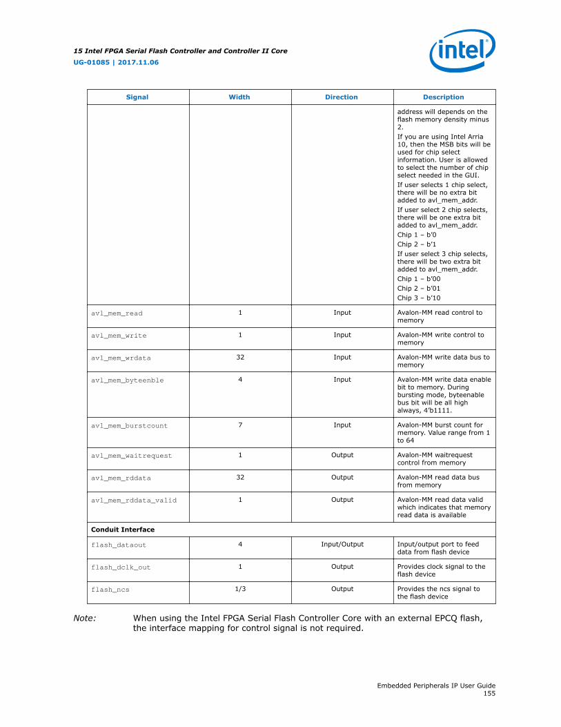
Signal Width Direction Description
address will depends on theflash memory density minus2.If you are using Intel Arria10, then the MSB bits will beused for chip selectinformation. User is allowedto select the number of chipselect needed in the GUI.If user selects 1 chip select,there will be no extra bitadded to avl_mem_addr.If user select 2 chip selects,there will be one extra bitadded to avl_mem_addr.Chip 1 – b’0Chip 2 – b’1If user select 3 chip selects,there will be two extra bitadded to avl_mem_addr.Chip 1 – b’00Chip 2 – b’01Chip 3 – b’10
avl_mem_read 1 Input Avalon-MM read control tomemory
avl_mem_write 1 Input Avalon-MM write control tomemory
avl_mem_wrdata 32 Input Avalon-MM write data bus tomemory
avl_mem_byteenble 4 Input Avalon-MM write data enablebit to memory. Duringbursting mode, byteenablebus bit will be all highalways, 4’b1111.
avl_mem_burstcount 7 Input Avalon-MM burst count formemory. Value range from 1to 64
avl_mem_waitrequest 1 Output Avalon-MM waitrequestcontrol from memory
avl_mem_rddata 32 Output Avalon-MM read data busfrom memory
avl_mem_rddata_valid 1 Output Avalon-MM read data validwhich indicates that memoryread data is available
Conduit Interface
flash_dataout 4 Input/Output Input/output port to feeddata from flash device
flash_dclk_out 1 Output Provides clock signal to theflash device
flash_ncs 1/3 Output Provides the ncs signal tothe flash device
Note: When using the Intel FPGA Serial Flash Controller Core with an external EPCQ flash,the interface mapping for control signal is not required.
15 Intel FPGA Serial Flash Controller and Controller II Core
UG-01085 | 2017.11.06
Embedded Peripherals IP User Guide155

15.2 Registers
15.2.1 Register Memory Map
Each address offset in the table below represents 1 word of memory address space.
Table 114. Register Memory Map
Register Offset Width Access Description
FLASH_RD_STATUS 0x0 8 R Perform read operation on flash devicestatus register and store the read backdata.
FLASH_RD_SID 0x1 8 R Perform read operation to extract flashdevice silicon ID and store the read backdata. Only support in EPCS16 and EPCS64flash devices.
FLASH_RD_RDID 0x2 8 R Perform read operation to extract flashdevice memory capacity and store the readback data.
FLASH_MEM_OP 0x3 24 W To protect and erase memory
FLASH_ISR 0x4 2 RW Interrupt status register
FLASH_IMR 0x5 2 RW To mask of interrupt status register
FLASH_CHIP_SELECT 0x6 3 W Chip select values:• B’000/b’001 -chip 1• B'010 - chip 2• B'100 - chip 3
15.2.2 Register Descriptions
15.2.2.1 FLASH_RD_STATUS
Table 115. FLASH_RD_STATUS
Bit Fields
31 30 29 28 27 26 25 24 23 22 21 20 19 18 17 16
Reserved
15 14 13 12 11 10 9 8 7 6 5 4 3 2 1 0
Reserved Read_status
15 Intel FPGA Serial Flash Controller and Controller II Core
UG-01085 | 2017.11.06
Embedded Peripherals IP User Guide156
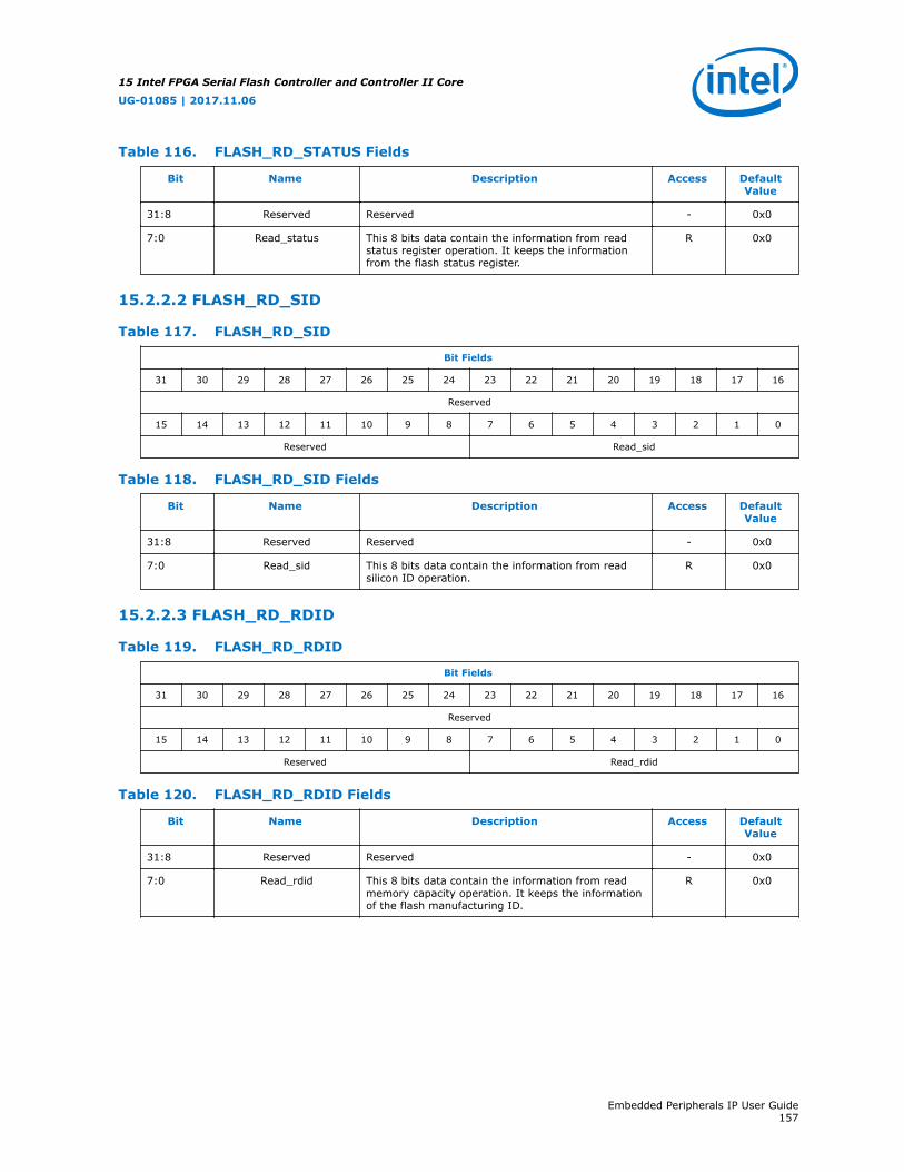
Table 116. FLASH_RD_STATUS Fields
Bit Name Description Access DefaultValue
31:8 Reserved Reserved - 0x0
7:0 Read_status This 8 bits data contain the information from readstatus register operation. It keeps the informationfrom the flash status register.
R 0x0
15.2.2.2 FLASH_RD_SID
Table 117. FLASH_RD_SID
Bit Fields
31 30 29 28 27 26 25 24 23 22 21 20 19 18 17 16
Reserved
15 14 13 12 11 10 9 8 7 6 5 4 3 2 1 0
Reserved Read_sid
Table 118. FLASH_RD_SID Fields
Bit Name Description Access DefaultValue
31:8 Reserved Reserved - 0x0
7:0 Read_sid This 8 bits data contain the information from readsilicon ID operation.
R 0x0
15.2.2.3 FLASH_RD_RDID
Table 119. FLASH_RD_RDID
Bit Fields
31 30 29 28 27 26 25 24 23 22 21 20 19 18 17 16
Reserved
15 14 13 12 11 10 9 8 7 6 5 4 3 2 1 0
Reserved Read_rdid
Table 120. FLASH_RD_RDID Fields
Bit Name Description Access DefaultValue
31:8 Reserved Reserved - 0x0
7:0 Read_rdid This 8 bits data contain the information from readmemory capacity operation. It keeps the informationof the flash manufacturing ID.
R 0x0
15 Intel FPGA Serial Flash Controller and Controller II Core
UG-01085 | 2017.11.06
Embedded Peripherals IP User Guide157
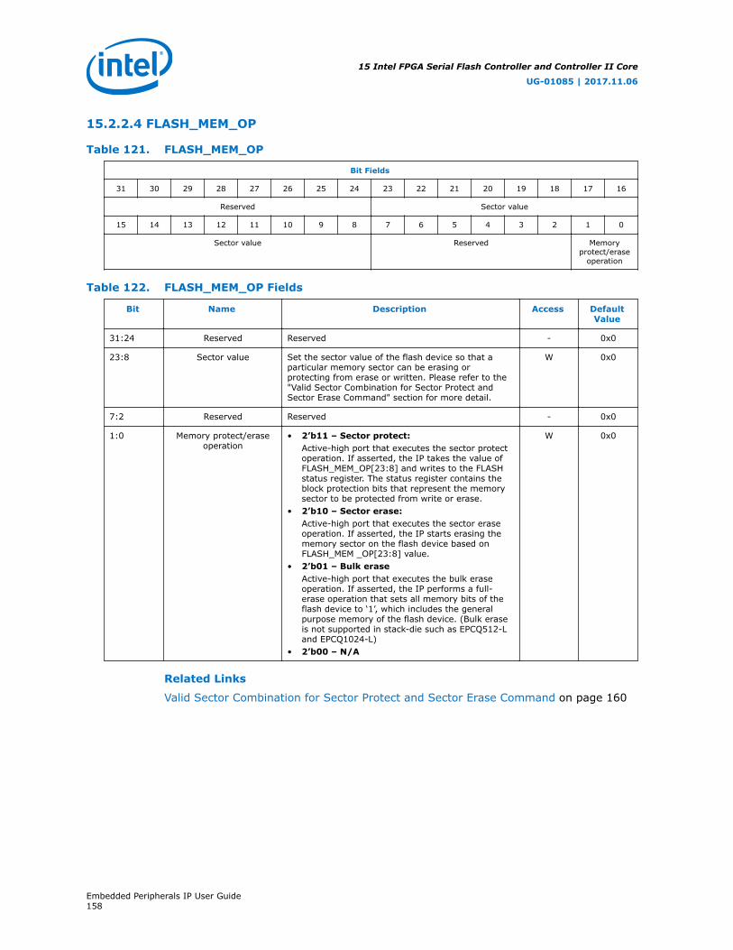
15.2.2.4 FLASH_MEM_OP
Table 121. FLASH_MEM_OP
Bit Fields
31 30 29 28 27 26 25 24 23 22 21 20 19 18 17 16
Reserved Sector value
15 14 13 12 11 10 9 8 7 6 5 4 3 2 1 0
Sector value Reserved Memoryprotect/erase
operation
Table 122. FLASH_MEM_OP Fields
Bit Name Description Access DefaultValue
31:24 Reserved Reserved - 0x0
23:8 Sector value Set the sector value of the flash device so that aparticular memory sector can be erasing orprotecting from erase or written. Please refer to the"Valid Sector Combination for Sector Protect andSector Erase Command" section for more detail.
W 0x0
7:2 Reserved Reserved - 0x0
1:0 Memory protect/eraseoperation
• 2’b11 – Sector protect:Active-high port that executes the sector protectoperation. If asserted, the IP takes the value ofFLASH_MEM_OP[23:8] and writes to the FLASHstatus register. The status register contains theblock protection bits that represent the memorysector to be protected from write or erase.
• 2’b10 – Sector erase:Active-high port that executes the sector eraseoperation. If asserted, the IP starts erasing thememory sector on the flash device based onFLASH_MEM _OP[23:8] value.
• 2’b01 – Bulk eraseActive-high port that executes the bulk eraseoperation. If asserted, the IP performs a full-erase operation that sets all memory bits of theflash device to ‘1’, which includes the generalpurpose memory of the flash device. (Bulk eraseis not supported in stack-die such as EPCQ512-Land EPCQ1024-L)
• 2’b00 – N/A
W 0x0
Related Links
Valid Sector Combination for Sector Protect and Sector Erase Command on page 160
15 Intel FPGA Serial Flash Controller and Controller II Core
UG-01085 | 2017.11.06
Embedded Peripherals IP User Guide158
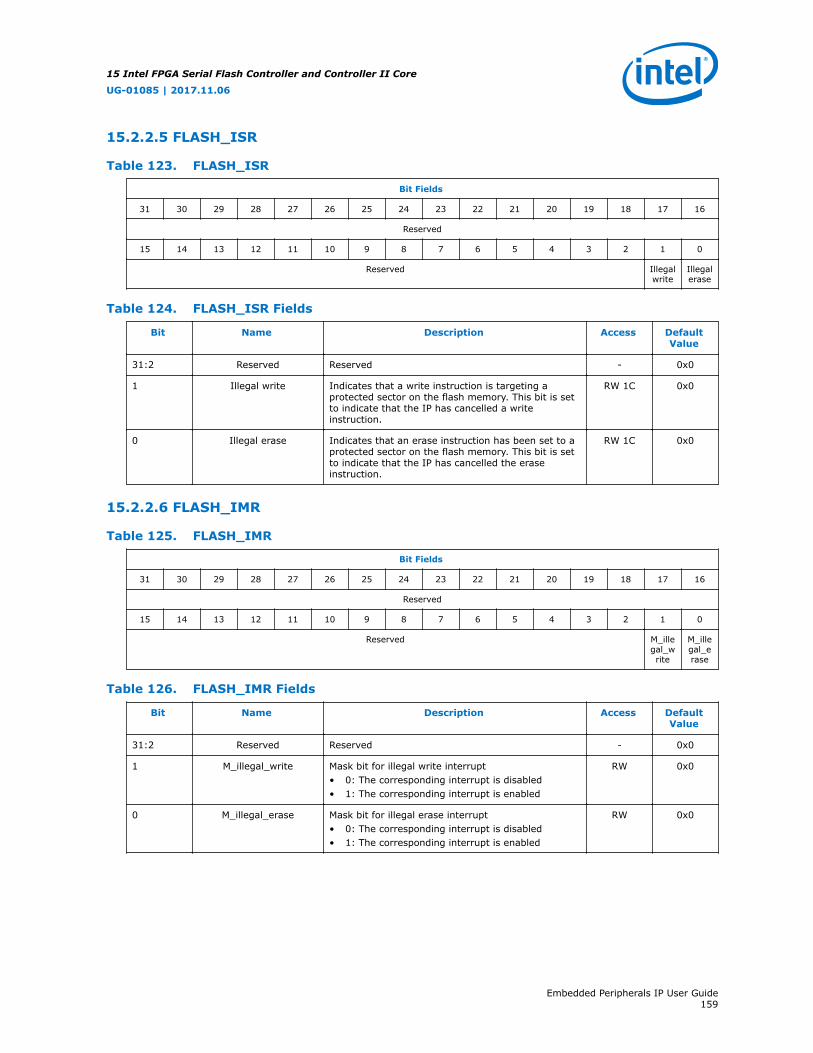
15.2.2.5 FLASH_ISR
Table 123. FLASH_ISR
Bit Fields
31 30 29 28 27 26 25 24 23 22 21 20 19 18 17 16
Reserved
15 14 13 12 11 10 9 8 7 6 5 4 3 2 1 0
Reserved Illegalwrite
Illegalerase
Table 124. FLASH_ISR Fields
Bit Name Description Access DefaultValue
31:2 Reserved Reserved - 0x0
1 Illegal write Indicates that a write instruction is targeting aprotected sector on the flash memory. This bit is setto indicate that the IP has cancelled a writeinstruction.
RW 1C 0x0
0 Illegal erase Indicates that an erase instruction has been set to aprotected sector on the flash memory. This bit is setto indicate that the IP has cancelled the eraseinstruction.
RW 1C 0x0
15.2.2.6 FLASH_IMR
Table 125. FLASH_IMR
Bit Fields
31 30 29 28 27 26 25 24 23 22 21 20 19 18 17 16
Reserved
15 14 13 12 11 10 9 8 7 6 5 4 3 2 1 0
Reserved M_illegal_write
M_illegal_erase
Table 126. FLASH_IMR Fields
Bit Name Description Access DefaultValue
31:2 Reserved Reserved - 0x0
1 M_illegal_write Mask bit for illegal write interrupt• 0: The corresponding interrupt is disabled• 1: The corresponding interrupt is enabled
RW 0x0
0 M_illegal_erase Mask bit for illegal erase interrupt• 0: The corresponding interrupt is disabled• 1: The corresponding interrupt is enabled
RW 0x0
15 Intel FPGA Serial Flash Controller and Controller II Core
UG-01085 | 2017.11.06
Embedded Peripherals IP User Guide159
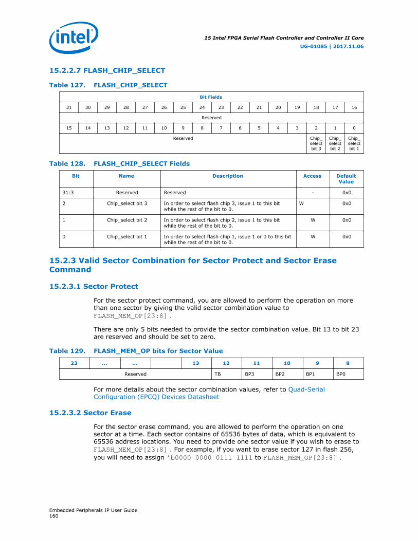
15.2.2.7 FLASH_CHIP_SELECT
Table 127. FLASH_CHIP_SELECT
Bit Fields
31 30 29 28 27 26 25 24 23 22 21 20 19 18 17 16
Reserved
15 14 13 12 11 10 9 8 7 6 5 4 3 2 1 0
Reserved Chip_selectbit 3
Chip_selectbit 2
Chip_selectbit 1
Table 128. FLASH_CHIP_SELECT Fields
Bit Name Description Access DefaultValue
31:3 Reserved Reserved - 0x0
2 Chip_select bit 3 In order to select flash chip 3, issue 1 to this bitwhile the rest of the bit to 0.
W 0x0
1 Chip_select bit 2 In order to select flash chip 2, issue 1 to this bitwhile the rest of the bit to 0.
W 0x0
0 Chip_select bit 1 In order to select flash chip 1, issue 1 or 0 to this bitwhile the rest of the bit to 0.
W 0x0
15.2.3 Valid Sector Combination for Sector Protect and Sector EraseCommand
15.2.3.1 Sector Protect
For the sector protect command, you are allowed to perform the operation on morethan one sector by giving the valid sector combination value toFLASH_MEM_OP[23:8] .
There are only 5 bits needed to provide the sector combination value. Bit 13 to bit 23are reserved and should be set to zero.
Table 129. FLASH_MEM_OP bits for Sector Value
23 ... ... 13 12 11 10 9 8
Reserved TB BP3 BP2 BP1 BP0
For more details about the sector combination values, refer to Quad-SerialConfiguration (EPCQ) Devices Datasheet
15.2.3.2 Sector Erase
For the sector erase command, you are allowed to perform the operation on onesector at a time. Each sector contains of 65536 bytes of data, which is equivalent to65536 address locations. You need to provide one sector value if you wish to erase toFLASH_MEM_OP[23:8] . For example, if you want to erase sector 127 in flash 256,you will need to assign ’b0000 0000 0111 1111 to FLASH_MEM_OP[23:8] .
15 Intel FPGA Serial Flash Controller and Controller II Core
UG-01085 | 2017.11.06
Embedded Peripherals IP User Guide160
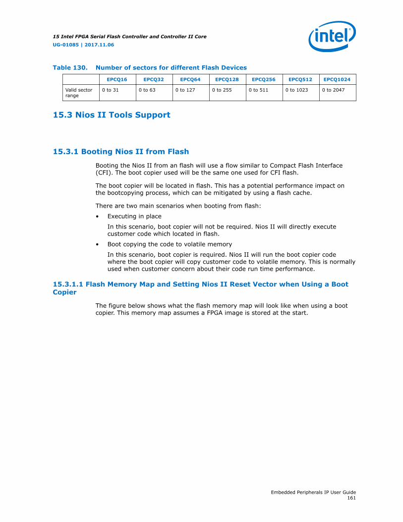
Table 130. Number of sectors for different Flash Devices
EPCQ16 EPCQ32 EPCQ64 EPCQ128 EPCQ256 EPCQ512 EPCQ1024
Valid sectorrange
0 to 31 0 to 63 0 to 127 0 to 255 0 to 511 0 to 1023 0 to 2047
15.3 Nios II Tools Support
15.3.1 Booting Nios II from Flash
Booting the Nios II from an flash will use a flow similar to Compact Flash Interface(CFI). The boot copier used will be the same one used for CFI flash.
The boot copier will be located in flash. This has a potential performance impact onthe bootcopying process, which can be mitigated by using a flash cache.
There are two main scenarios when booting from flash:
• Executing in place
In this scenario, boot copier will not be required. Nios II will directly executecustomer code which located in flash.
• Boot copying the code to volatile memory
In this scenario, boot copier is required. Nios II will run the boot copier codewhere the boot copier will copy customer code to volatile memory. This is normallyused when customer concern about their code run time performance.
15.3.1.1 Flash Memory Map and Setting Nios II Reset Vector when Using a BootCopier
The figure below shows what the flash memory map will look like when using a bootcopier. This memory map assumes a FPGA image is stored at the start.
15 Intel FPGA Serial Flash Controller and Controller II Core
UG-01085 | 2017.11.06
Embedded Peripherals IP User Guide161

Figure 50. EPCQ Flash Layout When Using Boot Copier
Customer Data (*.hex)
FPGA Image (*.sof)0x00000000
0x0000E400
Boot Copier
Application Code
0x01E0E400
At the start of the memory map is the FPGA image, followed by the boot copier, theapplication and then customer data. The size of the FPGA image is unknown and theexact size can only be known after the Intel Quartus Prime compile. However, the NiosII Reset Vector must be set in Platform Designer and must point to right after theFPGA image (i.e. the start of the boot copier).
The customer will have to determine an upper bound for the size of the FPGA imageand will have to set the Nios II Reset Vector in Platform Designer to start after theFPGA image(s).
15.3.1.2 Boot Copier File
The boot copier that will be used is the CFI boot copier, also known as memcpy-basedboot copier. We will provide the boot copier in one or more of the following formats:Intel HEX, Quartus HEX or SREC.
15.3.1.3 When Nios II SBT will Append a Boot Copier
The Nios II SBT tools know whether to append a boot copier based on the .text linkersection location. If the .text linker section is located in a different memory than wherethe reset vector points, it indicates a code copy is required. At this scenario a bootcopier is required. You can use the existing logic to generate a programming file withor without a boot copier depending on the scenario.
15 Intel FPGA Serial Flash Controller and Controller II Core
UG-01085 | 2017.11.06
Embedded Peripherals IP User Guide162

15.3.1.4 Creating HEX Programming File
The Nios II Software Build Tools (SBT) application Makefile “make mem_init_generate”target is responsible for generating memory initialization files. This includes generatingprogramming files (SREC, HEX) used for flashing a flash memory and files forinitializing memory (DAT, HEX) in simulation.
In boot scenario 1 (Executing in place), “make mem_init_generate” should generate aHEX file containing ELF loadable sections
In boot scenario 2 (Boot copying the code to volatile memory), “makemem_init_generate” should generate a HEX file containing both the boot copier andELF payload. “make mem_init_generate” is callable from SBT.
15.3.1.5 Programming the Flash
Programming the flash is done by using quartus_cpf to combine a compiled FPGAimage (SOF) with an application image (HEX file generated by Nios II SBT). The resultof this combination is a (POF) which can be programmed to the flash using the IntelQuartus Prime Programmer.
In the Intel Quartus Prime software, "Convert Programming File tool" (quartus_cpf)can be called by selecting File >> Convert Programming Files.
15.3.1.6 Custom Boot Copiers
Custom boot copiers can be used. “make mem_init_generate” calls conversion toolsunder the hood for creating programming files from compiled ELFs. These tools have aboot option to specify a custom boot copier. A user will need to call these underlyingconversion tools to generate a programming file with a custom boot copier.
15.3.1.7 Executing in Place
Executing in place shouldn’t be any different than executing in place with an On-chipRAM. As long as both the Nios II reset and exception vectors point to the flashmemory, execution will happen in place.
The Nios II board support package (BSP) settings are edited to enable alt_loadfunction to copy the writable memory section into volatile memory and keep the readonly section in the flash memory.
15.3.2 Nios II HAL Driver
A Nios II HAL driver will be developed similar to the driver’s currently available for CFI(altera_avalon_cfi_flash) and EPCS (altera_avalon_epcs_flash_controller).
Nios II HAL supports a number of generic device model classes including one fordevice flashes. Developing against these generic classes gives a consistent interfacefor driver functions so that the HAL can access the driver functions uniformly.
Please refer to the Flash Device Drivers section in the Developing Device Drivers forthe Hardware Abstraction Layer for more information.
Related Links
• Nios II Processor Booting From Intel FPGA Serial Flash (EPCQ)
15 Intel FPGA Serial Flash Controller and Controller II Core
UG-01085 | 2017.11.06
Embedded Peripherals IP User Guide163

• Developing Device Drivers for the Hardware Abstraction Layer
15.4 Intel FPGA Serial Flash Controller II
The Intel FPGA Serial Flash Controller II wraps around the Intel FPGA ASMI2 ParallelIP, and consists of some conversion logic which converts the ASMI Parallel conduitinterface to Avalon interface.
15.4.1 Register Memory Map
Each address offset in the table below represents 1 word of memory address space.
Table 131. Register Memory Map
Register Offset Width Access Description
FLASH_RD_STATUS 0x0 8 R Perform read operation on flash devicestatus register and store the read backdata.
FLASH_RD_RDID 0x2 8 R Perform read operation to extract flashdevice memory capacity and store the readback data.
FLASH_MEM_OP 0x3 24 W To protect and erase memory
FLASH_ISR 0x4 2 RW Interrupt status register
FLASH_IMR 0x5 2 RW To mask of interrupt status register
FLASH_CHIP_SELECT 0x6 3 W Chip select values:• B’000/b’001 -chip 1• B'010 - chip 2• B'100 - chip 3
EPCQ_FLAG_STATUS 0x7 8 RW Perform write/read operation to clear/readflag status from the device.
DEVICE_ID_DATA_0 0x8 32 R First word of device ID data
DEVICE_ID_DATA_1 0x9 32 R Second word of device ID data
DEVICE_ID_DATA_2 0x10 32 R Third word of device ID data
DEVICE_ID_DATA_3 0x11 32 R Fourth word of device ID data
DEVICE_ID_DATA_4 0x12 32 R Fifth word of device ID data
15.4.2 Configuration Device Types
The following device types can be selected through the configuration device type dropdown menu. Here you can specify the EPCQ.
• EPCQ16
• EPCQ32
• EPCQ64
• EPCQ128
• EPCQ256
• EPCQ512
15 Intel FPGA Serial Flash Controller and Controller II Core
UG-01085 | 2017.11.06
Embedded Peripherals IP User Guide164

• EPCQL256
• EPCQL512
• EPCQL1024
While using EPCS, EPCQ, or EPCQL device for Intel FPGA Serial Flash Controller II, youmust set MSEL pins for AS or ASx4 configuration scheme.
15.5 Document Revision History
Table 132. Intel FPGA Serial Flash Controller and Controller II Core Revision History
Date Version Changes
November 2017 2017.11.06 Added new configuration device types.
May 2017 2017.05.08 New section added:• Intel FPGA Serial Flash Controller II on page 164
June 2015 2015.06.12 Initial release.
15 Intel FPGA Serial Flash Controller and Controller II Core
UG-01085 | 2017.11.06
Embedded Peripherals IP User Guide165
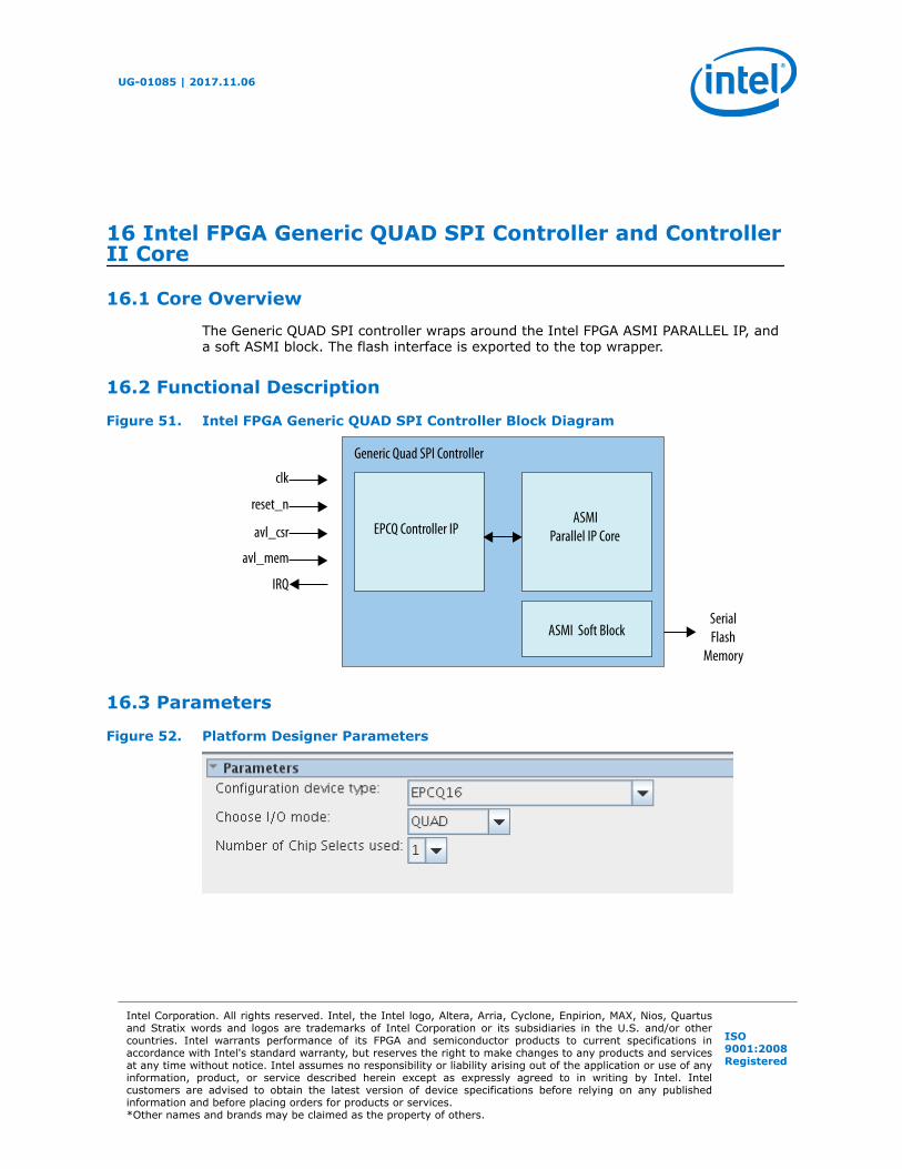
16 Intel FPGA Generic QUAD SPI Controller and ControllerII Core
16.1 Core Overview
The Generic QUAD SPI controller wraps around the Intel FPGA ASMI PARALLEL IP, anda soft ASMI block. The flash interface is exported to the top wrapper.
16.2 Functional Description
Figure 51. Intel FPGA Generic QUAD SPI Controller Block Diagram
Generic Quad SPI Controller
ASMI Parallel IP Core
ASMI Soft Block
EPCQ Controller IP
Serial Flash
Memory
clk
reset_n
avl_csr
avl_mem
IRQ
16.3 Parameters
Figure 52. Platform Designer Parameters
UG-01085 | 2017.11.06
Intel Corporation. All rights reserved. Intel, the Intel logo, Altera, Arria, Cyclone, Enpirion, MAX, Nios, Quartusand Stratix words and logos are trademarks of Intel Corporation or its subsidiaries in the U.S. and/or othercountries. Intel warrants performance of its FPGA and semiconductor products to current specifications inaccordance with Intel's standard warranty, but reserves the right to make changes to any products and servicesat any time without notice. Intel assumes no responsibility or liability arising out of the application or use of anyinformation, product, or service described herein except as expressly agreed to in writing by Intel. Intelcustomers are advised to obtain the latest version of device specifications before relying on any publishedinformation and before placing orders for products or services.*Other names and brands may be claimed as the property of others.
ISO9001:2008Registered
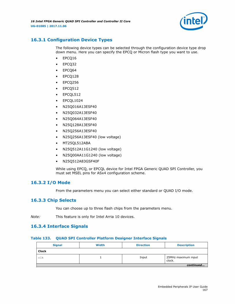
16.3.1 Configuration Device Types
The following device types can be selected through the configuration device type dropdown menu. Here you can specify the EPCQ or Micron flash type you want to use.
• EPCQ16
• EPCQ32
• EPCQ64
• EPCQ128
• EPCQ256
• EPCQ512
• EPCQL512
• EPCQL1024
• N25Q016A13ESF40
• N25Q032A13ESF40
• N25Q064A13ESF40
• N25Q128A13ESF40
• N25Q256A13ESF40
• N25Q256A13ESF40 (low voltage)
• MT25QL512ABA
• N25Q512A11G1240 (low voltage)
• N25Q00AA11G1240 (low voltage)
• N25Q512A83GSF40F
While using EPCQ, or EPCQL device for Intel FPGA Generic QUAD SPI Controller, youmust set MSEL pins for ASx4 configuration scheme.
16.3.2 I/O Mode
From the parameters menu you can select either standard or QUAD I/O mode.
16.3.3 Chip Selects
You can choose up to three flash chips from the parameters menu.
Note: This feature is only for Intel Arria 10 devices.
16.3.4 Interface Signals
Table 133. QUAD SPI Controller Platform Designer Interface Signals
Signal Width Direction Description
Clock
clk 1 Input 25MHz maximum inputclock.
continued...
16 Intel FPGA Generic QUAD SPI Controller and Controller II Core
UG-01085 | 2017.11.06
Embedded Peripherals IP User Guide167
Signal Width Direction Description
Reset
reset_n 1 Input Asynchronous reset used toreset QUAD SPI controller
Avalon-MM Slave Interface for CSR (avl_csr)
avl_csr_addr 3 Input Avalon-MM address bus. Theaddress bus is in wordaddressing.
avl_csr_read 1 Input Avalon-MM read control tocsr
avl_csr_write 1 Input Avalon-MM write control tocsr
avl_csr_waitrequest 1 Output Avalon-MM waitrequestcontrol from csr
avl_csr_wrdata 32 Input Avalon-MM write data bus tocsr
avl_csr_rddata 32 Output Avalon-MM read data busfrom csr
avl_csr_rddata_valid 1 Output Avalon-MM read data validwhich indicates that csr readdata is available
Interrupt Signals
irq 1 Output Interrupt signal to determineif there is an illegal write orillegal erase
Avalon-MM Slave Interface for Memory Access (avl_ mem)
avl_mem_addr * Input Avalon-MM address bus. Theaddress bus is in wordaddressing. The width of theaddress will depends on theflash memory density minus2.If you are using Intel Arria10, then the MSB bits will beused for chip selectinformation. User is allowedto select the number of chipselect needed in the GUI.If user selects 1 chip select,there will be no extra bitadded to avl_mem_addr.If user select 2 chip selects,there will be one extra bitadded to avl_mem_addr.Chip 1 – b’0Chip 2 – b’1If user select 3 chip selects,there will be two extra bitadded to avl_mem_addr.Chip 1 – b’00Chip 2 – b’01Chip 3 – b’10
avl_mem_read 1 Input Avalon-MM read control tomemory
continued...
16 Intel FPGA Generic QUAD SPI Controller and Controller II Core
UG-01085 | 2017.11.06
Embedded Peripherals IP User Guide168

Signal Width Direction Description
avl_mem_write 1 Input Avalon-MM write control tomemory
avl_mem_wrdata 32 Input Avalon-MM write data bus tomemory
avl_mem_byteenble 4 Input Avalon-MM write data enablebit to memory. Duringbursting mode, byteenablebus bit will be all highalways, 4’b1111.
avl_mem_burstcount 7 Input Avalon-MM burst count formemory. Value range from 1to 64
avl_mem_waitrequest 1 Output Avalon-MM waitrequestcontrol from memory
avl_mem_rddata 32 Output Avalon-MM read data busfrom memory
avl_mem_rddata_valid 1 Output Avalon-MM read data validwhich indicates that memoryread data is available
Conduit Interface
flash_dataout 4 Input/Output Input/output port to feeddata from flash device
flash_dclk_out 1 Output Provides clock signal to theflash device
flash_ncs 1/3 Output Provides the ncs signal tothe flash device
16.4 Registers
16.4.1 Register Memory Map
Each address offset in the table below represents 1 word of memory address space.
Table 134. Register Memory Map
Register Offset Width Access Description
FLASH_RD_STATUS 0x0 8 R Perform read operation on flash devicestatus register and store the read backdata.
FLASH_RD_SID 0x1 8 R Perform read operation to extract flashdevice silicon ID and store the read backdata. Only support in EPCS16 and EPCS64flash devices.
FLASH_RD_RDID 0x2 8 R Perform read operation to extract flashdevice memory capacity and store the readback data.
FLASH_MEM_OP 0x3 24 W To protect and erase memory
continued...
16 Intel FPGA Generic QUAD SPI Controller and Controller II Core
UG-01085 | 2017.11.06
Embedded Peripherals IP User Guide169

Register Offset Width Access Description
FLASH_ISR 0x4 2 RW Interrupt status register
FLASH_IMR 0x5 2 RW To mask of interrupt status register
FLASH_CHIP_SELECT 0x6 3 W Chip select values:• B’000/b’001 -chip 1• B'010 - chip 2• B'100 - chip 3
16.4.2 Register Descriptions
16.4.2.1 FLASH_RD_STATUS
Table 135. FLASH_RD_STATUS
Bit Fields
31 30 29 28 27 26 25 24 23 22 21 20 19 18 17 16
Reserved
15 14 13 12 11 10 9 8 7 6 5 4 3 2 1 0
Reserved Read_status
Table 136. FLASH_RD_STATUS Fields
Bit Name Description Access DefaultValue
31:8 Reserved Reserved - 0x0
7:0 Read_status This 8 bits data contain the information from readstatus register operation. It keeps the informationfrom the flash status register.
R 0x0
16.4.2.2 FLASH_RD_SID
Table 137. FLASH_RD_SID
Bit Fields
31 30 29 28 27 26 25 24 23 22 21 20 19 18 17 16
Reserved
15 14 13 12 11 10 9 8 7 6 5 4 3 2 1 0
Reserved Read_sid
Table 138. FLASH_RD_SID Fields
Bit Name Description Access DefaultValue
31:8 Reserved Reserved - 0x0
7:0 Read_sid This 8 bits data contain the information from readsilicon ID operation.
R 0x0
16 Intel FPGA Generic QUAD SPI Controller and Controller II Core
UG-01085 | 2017.11.06
Embedded Peripherals IP User Guide170
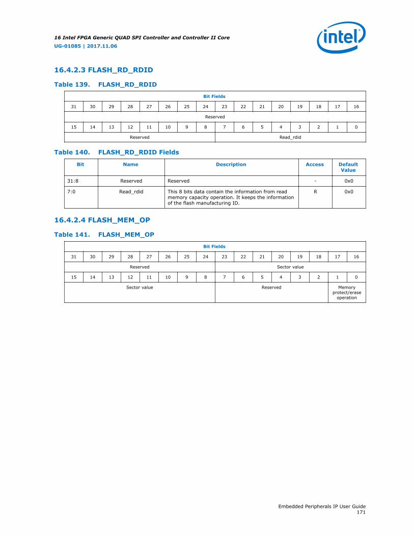
16.4.2.3 FLASH_RD_RDID
Table 139. FLASH_RD_RDID
Bit Fields
31 30 29 28 27 26 25 24 23 22 21 20 19 18 17 16
Reserved
15 14 13 12 11 10 9 8 7 6 5 4 3 2 1 0
Reserved Read_rdid
Table 140. FLASH_RD_RDID Fields
Bit Name Description Access DefaultValue
31:8 Reserved Reserved - 0x0
7:0 Read_rdid This 8 bits data contain the information from readmemory capacity operation. It keeps the informationof the flash manufacturing ID.
R 0x0
16.4.2.4 FLASH_MEM_OP
Table 141. FLASH_MEM_OP
Bit Fields
31 30 29 28 27 26 25 24 23 22 21 20 19 18 17 16
Reserved Sector value
15 14 13 12 11 10 9 8 7 6 5 4 3 2 1 0
Sector value Reserved Memoryprotect/erase
operation
16 Intel FPGA Generic QUAD SPI Controller and Controller II Core
UG-01085 | 2017.11.06
Embedded Peripherals IP User Guide171

Table 142. FLASH_MEM_OP Fields
Bit Name Description Access DefaultValue
31:18 Reserved Reserved - 0x0
23:8 Sector value Set the sector value of the flash device so that aparticular memory sector can be erasing orprotecting from erase or written. Please refer to the"Valid Sector Combination for Sector Protect andSector Erase Command" section for more detail.
W 0x0
7:2 Reserved Reserved - 0x0
1:0 Memory protect/eraseoperation
• 2’b11 – Sector protect:Active-high port that executes the sector protectoperation. If asserted, the IP takes the value ofFLASH_MEM_OP[23:8] and writes to the FLASHstatus register. The status register contains theblock protection bits that represent the memorysector to be protected from write or erase.
• 2’b10 – Sector erase:Active-high port that executes the sector eraseoperation. If asserted, the IP starts erasing thememory sector on the flash device based onFLASH_MEM _OP[23:8] value.
• 2’b01 – Bulk eraseActive-high port that executes the bulk eraseoperation. If asserted, the IP performs a full-erase operation that sets all memory bits of theflash device to ‘1’, which includes the generalpurpose memory of the flash device. (Bulk eraseis not supported in stack-die such as EPCQ512-Land EPCQ1024-L)
• 2’b00 – N/A
W 0x0
Related Links
Valid Sector Combination for Sector Protect and Sector Erase Command on page 174
16.4.2.5 FLASH_ISR
Table 143. FLASH_ISR
Bit Fields
31 30 29 28 27 26 25 24 23 22 21 20 19 18 17 16
Reserved
15 14 13 12 11 10 9 8 7 6 5 4 3 2 1 0
Reserved Illegalwrite
Illegalerase
16 Intel FPGA Generic QUAD SPI Controller and Controller II Core
UG-01085 | 2017.11.06
Embedded Peripherals IP User Guide172

Table 144. FLASH_ISR Fields
Bit Name Description Access DefaultValue
31:2 Reserved Reserved - 0x0
1 Illegal write Indicates that a write instruction is targeting aprotected sector on the flash memory. This bit is setto indicate that the IP has cancelled a writeinstruction.
RW 1C 0x0
0 Illegal erase Indicates that an erase instruction has been set to aprotected sector on the flash memory. This bit is setto indicate that the IP has cancelled the eraseinstruction.
RW 1C 0x0
16.4.2.6 FLASH_IMR
Table 145. FLASH_IMR
Bit Fields
31 30 29 28 27 26 25 24 23 22 21 20 19 18 17 16
Reserved
15 14 13 12 11 10 9 8 7 6 5 4 3 2 1 0
Reserved M_illegal_write
M_illegal_erase
Table 146. FLASH_IMR Fields
Bit Name Description Access DefaultValue
31:2 Reserved Reserved - 0x0
1 M_illegal_write Mask bit for illegal write interrupt• 0: The corresponding interrupt is disabled• 1: The corresponding interrupt is enabled
RW 0x0
0 M_illegal_erase Mask bit for illegal erase interrupt• 0: The corresponding interrupt is disabled• 1: The corresponding interrupt is enabled
RW 0x0
16.4.2.7 FLASH_CHIP_SELECT
Table 147. FLASH_CHIP_SELECT
Bit Fields
31 30 29 28 27 26 25 24 23 22 21 20 19 18 17 16
Reserved
15 14 13 12 11 10 9 8 7 6 5 4 3 2 1 0
Reserved Chip_selectbit 3
Chip_selectbit 2
Chip_selectbit 1
16 Intel FPGA Generic QUAD SPI Controller and Controller II Core
UG-01085 | 2017.11.06
Embedded Peripherals IP User Guide173
Table 148. FLASH_CHIP_SELECT Fields
Bit Name Description Access DefaultValue
31:3 Reserved Reserved - 0x0
2 Chip_select bit 3 In order to select flash chip 3, issue 1 to this bitwhile the rest of the bit to 0.
W 0x0
1 Chip_select bit 2 In order to select flash chip 2, issue 1 to this bitwhile the rest of the bit to 0.
W 0x0
0 Chip_select bit 1 In order to select flash chip 1, issue 1 or 0 to this bitwhile the rest of the bit to 0.
W 0x0
16.4.3 Valid Sector Combination for Sector Protect and Sector EraseCommand
16.4.3.1 Sector Protect
For the sector protect command, you are allowed to perform the operation on morethan one sector by giving the valid sector combination value toFLASH_MEM_OP[23:8] .
There are only 5 bits needed to provide the sector combination value. Bit 13 to bit 23are reserved and should be set to zero.
Table 149. FLASH_MEM_OP bits for Sector Value
23 ... ... 13 12 11 10 9 8
Reserved TB BP3 BP2 BP1 BP0
For more details about the sector combination values, refer to Quad-SerialConfiguration (EPCQ) Devices Datasheet
16.4.3.2 Sector Erase
For the sector erase command, you are allowed to perform the operation on onesector at a time. Each sector contains of 65536 bytes of data, which is equivalent to65536 address locations. You need to provide one sector value if you wish to erase toFLASH_MEM_OP[23:8] . For example, if you want to erase sector 127 in flash 256,you will need to assign ’b0000 0000 0111 1111 to FLASH_MEM_OP[23:8] .
Table 150. Number of sectors for different Flash Devices
EPCQ16 EPCQ32 EPCQ64 EPCQ128 EPCQ256 EPCQ512 EPCQ1024
Valid sectorrange
0 to 31 0 to 63 0 to 127 0 to 255 0 to 511 0 to 1023 0 to 2047
16.5 Nios II Tools Support
16 Intel FPGA Generic QUAD SPI Controller and Controller II Core
UG-01085 | 2017.11.06
Embedded Peripherals IP User Guide174
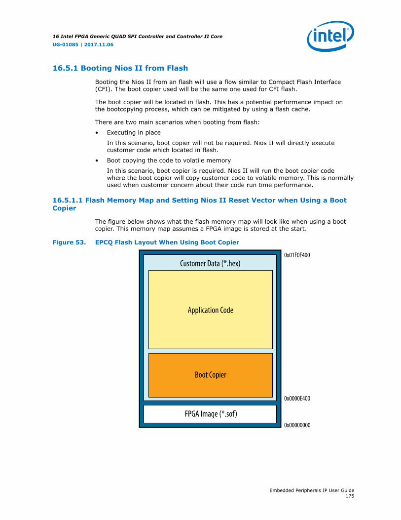
16.5.1 Booting Nios II from Flash
Booting the Nios II from an flash will use a flow similar to Compact Flash Interface(CFI). The boot copier used will be the same one used for CFI flash.
The boot copier will be located in flash. This has a potential performance impact onthe bootcopying process, which can be mitigated by using a flash cache.
There are two main scenarios when booting from flash:
• Executing in place
In this scenario, boot copier will not be required. Nios II will directly executecustomer code which located in flash.
• Boot copying the code to volatile memory
In this scenario, boot copier is required. Nios II will run the boot copier codewhere the boot copier will copy customer code to volatile memory. This is normallyused when customer concern about their code run time performance.
16.5.1.1 Flash Memory Map and Setting Nios II Reset Vector when Using a BootCopier
The figure below shows what the flash memory map will look like when using a bootcopier. This memory map assumes a FPGA image is stored at the start.
Figure 53. EPCQ Flash Layout When Using Boot Copier
Customer Data (*.hex)
FPGA Image (*.sof)0x00000000
0x0000E400
Boot Copier
Application Code
0x01E0E400
16 Intel FPGA Generic QUAD SPI Controller and Controller II Core
UG-01085 | 2017.11.06
Embedded Peripherals IP User Guide175
At the start of the memory map is the FPGA image, followed by the boot copier, theapplication and then customer data. The size of the FPGA image is unknown and theexact size can only be known after the Intel Quartus Prime compile. However, the NiosII Reset Vector must be set in Platform Designer and must point to right after theFPGA image (i.e. the start of the boot copier).
The customer will have to determine an upper bound for the size of the FPGA imageand will have to set the Nios II Reset Vector in Platform Designer to start after theFPGA image(s).
16.5.1.2 Boot Copier File
The boot copier that will be used is the CFI boot copier, also known as memcpy-basedboot copier. We will provide the boot copier in one or more of the following formats:Intel HEX, Quartus HEX or SREC.
16.5.1.3 When Nios II SBT will Append a Boot Copier
The Nios II SBT tools know whether to append a boot copier based on the .text linkersection location. If the .text linker section is located in a different memory than wherethe reset vector points, it indicates a code copy is required. At this scenario a bootcopier is required. You can use the existing logic to generate a programming file withor without a boot copier depending on the scenario.
16.5.1.4 Creating HEX Programming File
The Nios II Software Build Tools (SBT) application Makefile “make mem_init_generate”target is responsible for generating memory initialization files. This includes generatingprogramming files (SREC, HEX) used for flashing a flash memory and files forinitializing memory (DAT, HEX) in simulation.
In boot scenario 1 (Executing in place), “make mem_init_generate” should generate aHEX file containing ELF loadable sections
In boot scenario 2 (Boot copying the code to volatile memory), “makemem_init_generate” should generate a HEX file containing both the boot copier andELF payload. “make mem_init_generate” is callable from SBT.
16.5.1.5 Programming Flash
Programming the flash is done by using quartus_cpf to combine a compiled FPGAimage (SOF) with an application image (HEX file generated by Nios II SBT). The resultof this combination is a (POF) which can be programmed to the flash using the IntelQuartus Prime Programmer.
In the Intel Quartus Prime software, "Convert Programming File tool" (quartus_cpf)can be called by selecting File >> Convert Programming Files.
16.5.1.6 Custom Boot Copiers
Custom boot copiers can be used. “make mem_init_generate” calls conversion toolsunder the hood for creating programming files from compiled ELFs. These tools have aboot option to specify a custom boot copier. A user will need to call these underlyingconversion tools to generate a programming file with a custom boot copier.
16 Intel FPGA Generic QUAD SPI Controller and Controller II Core
UG-01085 | 2017.11.06
Embedded Peripherals IP User Guide176
16.5.1.7 Executing in Place
Executing in place shouldn’t be any different than executing in place with an On-chipRAM. As long as both the Nios II reset and exception vectors point to the flashmemory, execution will happen in place.
The Nios II board support package (BSP) settings are edited to enable alt_loadfunction to copy the writable memory section into volatile memory and keep the readonly section in the flash memory.
16.5.2 Nios II HAL Driver
A Nios II HAL driver will be developed similar to the driver’s currently available for CFI(altera_avalon_cfi_flash) and EPCS (altera_avalon_epcs_flash_controller).
Nios II HAL supports a number of generic device model classes including one fordevice flashes. Developing against these generic classes gives a consistent interfacefor driver functions so that the HAL can access the driver functions uniformly.
Please refer to the Flash Device Drivers section in the Developing Device Drivers forthe Hardware Abstraction Layer for more information.
Related Links
Developing Device Drivers for the Hardware Abstraction Layer
16.6 Intel FPGA Generic QUAD SPI Controller II
The Generic QUAD SPI Controller II wraps around the Intel FPGA ASMI2 PARALLEL IP,and a soft ASMI block. The flash interface is exported to the top wrapper.
16.6.1 Register Memory Map
Each address offset in the table below represents 1 word of memory address space.
Table 151. Register Memory Map
Register Offset Width Access Description
FLASH_RD_STATUS 0x0 8 R Perform read operation on flash devicestatus register and store the read backdata.
FLASH_RD_RDID 0x2 8 R Perform read operation to extract flashdevice memory capacity and store the readback data.
FLASH_MEM_OP 0x3 24 W To protect, erase, and write enable memory.To perform write enable operation, set thisregister with the value 3'b100.
FLASH_ISR 0x4 2 RW Interrupt status register
FLASH_IMR 0x5 2 RW To mask of interrupt status register
FLASH_CHIP_SELECT 0x6 3 W Chip select values:• B’000/b’001 -chip 1• B'010 - chip 2• B'100 - chip 3
continued...
16 Intel FPGA Generic QUAD SPI Controller and Controller II Core
UG-01085 | 2017.11.06
Embedded Peripherals IP User Guide177

Register Offset Width Access Description
EPCQ_FLAG_STATUS 0x7 8 RW Perform write/read operation to clear/readflag status from the device.
DEVICE_ID_DATA_0 0x8 32 R First word of device ID data
DEVICE_ID_DATA_1 0x9 32 R Second word of device ID data
DEVICE_ID_DATA_2 0x10 32 R Third word of device ID data
DEVICE_ID_DATA_3 0x11 32 R Fourth word of device ID data
DEVICE_ID_DATA_4 0x12 32 R Fifth word of device ID data
16.6.2 Configuration Device Types
The following device types can be selected through the configuration device type dropdown menu. Here you can specify the EPCQ or Micron flash type you want to use.
• EPCQ16
• EPCQ32
• EPCQ64
• EPCQ128
• EPCQ256
• EPCQ512
• EPCQL512
• EPCQL1024
• N25Q016A13ESF40
• N25Q032A13ESF40
• N25Q064A13ESF40
• N25Q128A13ESF40
• N25Q256A13ESF40
• N25Q256A11E1240 (low voltage)
• MT25QL512ABA
• N25Q512A11G1240 (low voltage)
• N25Q00AA11G1240 (low voltage)
• N25Q512A83GSF40F
While using EPCQ, or EPCQL device for Intel FPGA Generic QUAD SPI Controller II, youmust set MSEL pins for ASx4 configuration scheme.
16 Intel FPGA Generic QUAD SPI Controller and Controller II Core
UG-01085 | 2017.11.06
Embedded Peripherals IP User Guide178
16.7 Document Revision History
Table 152. Intel FPGA Generic QUAD SPI Controller and Controller II Core RevisionHistory
Date Version Changes
November 2017 2017.11.06 Added information about the write enable operation in Table: RegisterMemory Map for Intel FPGA Generic QUAD SPI Controller II core.
May 2017 2017.05.08 New section added:• Intel FPGA Generic QUAD SPI Controller II on page 177
June 2015 2015.06.12 Initial release.
16 Intel FPGA Generic QUAD SPI Controller and Controller II Core
UG-01085 | 2017.11.06
Embedded Peripherals IP User Guide179
17 Interval Timer Core
17.1 Core Overview
The Interval Timer core with Avalon interface is an interval timer for Avalon-basedprocessor systems, such as a Nios II processor system. The core provides thefollowing features:
• 32-bit and 64-bit counters.
• Controls to start, stop, and reset the timer.
• Two count modes: count down once and continuous count-down.
• Count-down period register.
• Option to enable or disable the interrupt request (IRQ) when timer reaches zero.
• Optional watchdog timer feature that resets the system if timer ever reaches zero.
• Optional periodic pulse generator feature that outputs a pulse when timer reacheszero.
• Compatible with 32-bit and 16-bit processors.
Device drivers are provided in the HAL system library for the Nios II processor.
17.2 Functional Description
Figure 54. Interval Timer Core Block Diagram
Register File
status
control
period_ n
snap_ n
IRQ
Address &Data
Avalon-MM slave interface
to on-chiplogic
ControlLogic
resetrequest
(watchdog)
timeout_pulse
Counter
UG-01085 | 2017.11.06
Intel Corporation. All rights reserved. Intel, the Intel logo, Altera, Arria, Cyclone, Enpirion, MAX, Nios, Quartusand Stratix words and logos are trademarks of Intel Corporation or its subsidiaries in the U.S. and/or othercountries. Intel warrants performance of its FPGA and semiconductor products to current specifications inaccordance with Intel's standard warranty, but reserves the right to make changes to any products and servicesat any time without notice. Intel assumes no responsibility or liability arising out of the application or use of anyinformation, product, or service described herein except as expressly agreed to in writing by Intel. Intelcustomers are advised to obtain the latest version of device specifications before relying on any publishedinformation and before placing orders for products or services.*Other names and brands may be claimed as the property of others.
ISO9001:2008Registered
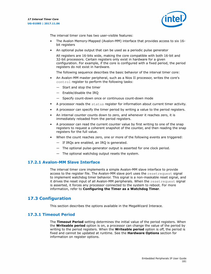
The interval timer core has two user-visible features:
• The Avalon Memory-Mapped (Avalon-MM) interface that provides access to six 16-bit registers
• An optional pulse output that can be used as a periodic pulse generator
All registers are 16-bits wide, making the core compatible with both 16-bit and32-bit processors. Certain registers only exist in hardware for a givenconfiguration. For example, if the core is configured with a fixed period, the periodregisters do not exist in hardware.
The following sequence describes the basic behavior of the interval timer core:
• An Avalon-MM master peripheral, such as a Nios II processor, writes the core'scontrol register to perform the following tasks:
— Start and stop the timer
— Enable/disable the IRQ
— Specify count-down once or continuous count-down mode
• A processor reads the status register for information about current timer activity.
• A processor can specify the timer period by writing a value to the period registers.
• An internal counter counts down to zero, and whenever it reaches zero, it isimmediately reloaded from the period registers.
• A processor can read the current counter value by first writing to one of the snapregisters to request a coherent snapshot of the counter, and then reading the snapregisters for the full value.
• When the count reaches zero, one or more of the following events are triggered:
— If IRQs are enabled, an IRQ is generated.
— The optional pulse-generator output is asserted for one clock period.
— The optional watchdog output resets the system.
17.2.1 Avalon-MM Slave Interface
The interval timer core implements a simple Avalon-MM slave interface to provideaccess to the register file. The Avalon-MM slave port uses the resetrequest signalto implement watchdog timer behavior. This signal is a non-maskable reset signal, andit drives the reset input of all Avalon-MM peripherals. When the resetrequest signalis asserted, it forces any processor connected to the system to reboot. For moreinformation, refer to Configuring the Timer as a Watchdog Timer.
17.3 Configuration
This section describes the options available in the MegaWizard Interace.
17.3.1 Timeout Period
The Timeout Period setting determines the initial value of the period registers. Whenthe Writeable period option is on, a processor can change the value of the period bywriting to the period registers. When the Writeable period option is off, the period isfixed and cannot be updated at runtime. See the Hardware Options section forinformation on register options.
17 Interval Timer Core
UG-01085 | 2017.11.06
Embedded Peripherals IP User Guide181

The Timeout Period is an integer multiple of the Timer Frequency. The TimerFrequency is fixed at the frequency setting of the system clock associated with thetimer. The Timeout Period setting can be specified in units of µs (microseconds), ms(milliseconds), seconds , or clocks (number of cycles of the system clock associatedwith the timer). The actual period depends on the frequency of the system clockassociated with the timer. If the period is specified in µs, ms, or seconds, the trueperiod will be the smallest number of clock cycles that is greater or equal to thespecified Timeout Period value. For example, if the associated system clock has afrequency of 30 ns, and the specified Timeout Period value is 1 µs, the true timeoutperiod will be 1.020 microseconds.
17.3.2 Counter Size
The Counter Size setting determines the timer's width, which can be set to either 32or 64 bits. A 32-bit timer has two 16-bit period registers, whereas a 64-bit timer hasfour 16-bit period registers. This option applies to the snap registers as well.
17.3.3 Hardware Options
The following options affect the hardware structure of the interval timer core. As aconvenience, the Preset Configurations list offers several pre-defined hardwareconfigurations, such as:
• Simple periodic interrupt—This configuration is useful for systems that requireonly a periodic IRQ generator. The period is fixed and the timer cannot bestopped, but the IRQ can be disabled.
• Full-featured—This configuration is useful for embedded processor systems thatrequire a timer with variable period that can be started and stopped underprocessor control.
• Watchdog—This configuration is useful for systems that require watchdog timerto reset the system in the event that the system has stopped responding. Refer tothe Configuring the Timer as a Watchdog Timer section.
Register Options
Table 153. Register Options
Option Description
Writeable period When this option is enabled, a master peripheral can change the count-down period by writing tothe period registers. When disabled, the count-down period is fixed at the specified TimeoutPeriod, and the period registers do not exist in hardware.
Readable snapshot When this option is enabled, a master peripheral can read a snapshot of the current count-down.When disabled, the status of the counter is detectable only via other indicators, such as the statusregister or the IRQ signal. In this case, the snap registers do not exist in hardware, and readingthese registers produces an undefined value.
Start/Stop controlbits
When this option is enabled, a master peripheral can start and stop the timer by writing the STARTand STOP bits in the control register. When disabled, the timer runs continuously. When theSystem reset on timeout (watchdog) option is enabled, the START bit is also present, regardlessof the Start/Stop control bits option.
17 Interval Timer Core
UG-01085 | 2017.11.06
Embedded Peripherals IP User Guide182
Output Signal Options
Table 154. Output Signal Options
Option Description
Timeout pulse(1 clock wide)
When this option is on, the core outputs a signal timeout_pulse. This signal pulses high for oneclock cycle whenever the timer reaches zero. When this option is off, the timeout_pulse signaldoes not exist.
System reset ontimeout (watchdog)
When this option is on, the core’s Avalon-MM slave port includes the resetrequest signal. Thissignal pulses high for one clock cycle whenever the timer reaches zero resulting in a system-widereset. The internal timer is stopped at reset. Explicitly writing the START bit of the control registerstarts the timer.When this option is off, the resetrequest signal does not exist.Refer to the Configuring the Timer as a Watchdog Timer section.
17.3.4 Configuring the Timer as a Watchdog Timer
To configure the core for use as a watchdog, in the MegaWizard Interface selectWatchdog in the Preset Configurations list, or choose the following settings:
• Set the Timeout Period to the desired "watchdog" period.
• Turn off Writeable period.
• Turn off Readable snapshot.
• Turn off Start/Stop control bits.
• Turn off Timeout pulse.
• Turn on System reset on timeout (watchdog).
A watchdog timer wakes up (comes out of reset) stopped. A processor later startsthe timer by writing a 1 to the control register's START bit. Once started, thetimer can never be stopped. If the internal counter ever reaches zero, thewatchdog timer resets the system by generating a pulse on its resetrequestoutput. The resetrequest pulse will last for two cycles before the incomingreset signal deasserts the pulse. To prevent an indefinite resetrequest pulse,you are required to connect the resetrequest signal back to the reset input ofthe timer.
To prevent the system from resetting, the processor must periodically reset thetimer's count-down value by writing one of the period registers (the written valueis ignored). If the processor fails to access the timer because, for example,software stopped executing normally, the watchdog timer resets the system andreturns the system to a defined state.
17.4 Software Programming Model
The following sections describe the software programming model for the interval timercore, including the register map and software declarations to access the hardware. ForNios II processor users, Intel provides hardware abstraction layer (HAL) system librarydrivers that enable you to access the interval timer core using the HAL applicationprogramming interface (API) functions.
17 Interval Timer Core
UG-01085 | 2017.11.06
Embedded Peripherals IP User Guide183
17.4.1 HAL System Library Support
The Intel-provided drivers integrate into the HAL system library for Nios II systems.When possible, HAL users should access the core via the HAL API, rather thanaccessing the core's registers directly.
Intel provides a driver for both the HAL timer device models: system clock timer, andtimestamp timer.
System Clock Driver
When configured as the system clock, the interval timer core runs continuously inperiodic mode, using the default period set. The system clock services are then run asa part of the interrupt service routine for this timer. The driver is interrupt-driven, andtherefore must have its interrupt signal connected in the system hardware.
The Nios II integrated development environment (IDE) allows you to specify systemlibrary properties that determine which timer device will be used as the system clocktimer.
Timestamp Driver
The interval timer core may be used as a timestamp device if it meets the followingconditions:
• The timer has a writeable period register, as configured in Platform Designer.
• The timer is not selected as the system clock.
The Nios II IDE allows you to specify system library properties that determinewhich timer device will be used as the timestamp timer.
If the timer hardware is not configured with writeable period registers, calls tothe alt_timestamp_start() API function will not reset the timestamp counter.All other HAL API calls will perform as expected.
For more information about using the system clock and timestamp features thatuse these drivers, refer to the Nios II Software Developer’s Handbook. TheNios II Embedded Design Suite (EDS) also provides several example designs thatuse the interval timer core.
Limitations
The HAL driver for the interval timer core does not support the watchdog reset featureof the core.
17.4.2 Software Files
The interval timer core is accompanied by the following software files. These filesdefine the low-level interface to the hardware, and provide the HAL drivers.Application developers should not modify these files.
• altera_avalon_timer_regs.h—This file defines the core's register map,providing symbolic constants to access the low-level hardware.
• altera_avalon_timer.h, altera_avalon_timer_sc.c,altera_avalon_timer_ts.c, altera_avalon_timer_vars.c—These filesimplement the timer device drivers for the HAL system library.
17 Interval Timer Core
UG-01085 | 2017.11.06
Embedded Peripherals IP User Guide184
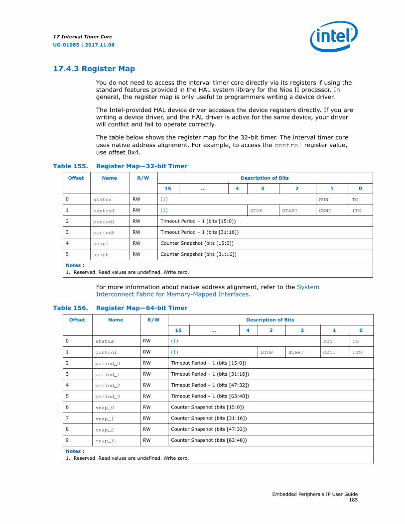
17.4.3 Register Map
You do not need to access the interval timer core directly via its registers if using thestandard features provided in the HAL system library for the Nios II processor. Ingeneral, the register map is only useful to programmers writing a device driver.
The Intel-provided HAL device driver accesses the device registers directly. If you arewriting a device driver, and the HAL driver is active for the same device, your driverwill conflict and fail to operate correctly.
The table below shows the register map for the 32-bit timer. The interval timer coreuses native address alignment. For example, to access the control register value,use offset 0x4.
Table 155. Register Map—32-bit Timer
Offset Name R/W Description of Bits
15 ... 4 3 2 1 0
0 status RW (1) RUN TO
1 control RW (1) STOP START CONT ITO
2 periodl RW Timeout Period – 1 (bits [15:0])
3 periodh RW Timeout Period – 1 (bits [31:16])
4 snapl RW Counter Snapshot (bits [15:0])
5 snaph RW Counter Snapshot (bits [31:16])
Notes :1. Reserved. Read values are undefined. Write zero.
For more information about native address alignment, refer to the SystemInterconnect Fabric for Memory-Mapped Interfaces.
Table 156. Register Map—64-bit Timer
Offset Name R/W Description of Bits
15 ... 4 3 2 1 0
0 status RW (1) RUN TO
1 control RW (1) STOP START CONT ITO
2 period_0 RW Timeout Period – 1 (bits [15:0])
3 period_1 RW Timeout Period – 1 (bits [31:16])
4 period_2 RW Timeout Period – 1 (bits [47:32])
5 period_3 RW Timeout Period – 1 (bits [63:48])
6 snap_0 RW Counter Snapshot (bits [15:0])
7 snap_1 RW Counter Snapshot (bits [31:16])
8 snap_2 RW Counter Snapshot (bits [47:32])
9 snap_3 RW Counter Snapshot (bits [63:48])
Notes :1. Reserved. Read values are undefined. Write zero.
17 Interval Timer Core
UG-01085 | 2017.11.06
Embedded Peripherals IP User Guide185

status Register
The status register has two defined bits.
Table 157. status Register Bits
Bit Name R/W/C Description
0 TO R/WC The TO (timeout) bit is set to 1 when the internal counter reaches zero. Once set by a timeoutevent, the TO bit stays set until explicitly cleared by a master peripheral. Write 0 or 1 to thestatus register to clear the TO bit.
1 RUN R The RUN bit reads as 1 when the internal counter is running; otherwise this bit reads as 0. TheRUN bit is not changed by a write operation to the status register.
control Register
The control register has four defined bits.
Table 158. control Register Bits
Bit Name R/W/C Description
0 ITO RW If the ITO bit is 1, the interval timer core generates an IRQ when the status register’s TObit is 1. When the ITO bit is 0, the timer does not generate IRQs.
1 CONT RW The CONT (continuous) bit determines how the internal counter behaves when it reaches zero.If the CONT bit is 1, the counter runs continuously until it is stopped by the STOP bit. If CONTis 0, the counter stops after it reaches zero. When the counter reaches zero, it reloads withthe value stored in the period registers, regardless of the CONT bit.
2 START (1) W Writing a 1 to the START bit starts the internal counter running (counting down). The STARTbit is an event bit that enables the counter when a write operation is performed. If the timeris stopped, writing a 1 to the START bit causes the timer to restart counting from the numbercurrently stored in its counter. If the timer is already running, writing a 1 to START has noeffect. Writing 0 to the START bit has no effect.
3 STOP (1) W Writing a 1 to the STOP bit stops the internal counter. The STOP bit is an event bit that causesthe counter to stop when a write operation is performed. If the timer is already stopped,writing a 1 to STOP has no effect. Writing a 0 to the stop bit has no effect.If the timer hardware is configured with Start/Stop control bits off, writing the STOP bithas no effect.
Notes :1. Writing 1 to both START and STOP bits simultaneously produces an undefined result.
17 Interval Timer Core
UG-01085 | 2017.11.06
Embedded Peripherals IP User Guide186
period_n Registers
The period_n registers together store the timeout period value. The internal counteris loaded with the value stored in these registers whenever one of the followingoccurs:
• A write operation to one of the period_n register
• The internal counter reaches 0
The timer's actual period is one cycle greater than the value stored in theperiod_n registers because the counter assumes the value zero for one clockcycle.
Writing to one of the period_n registers stops the internal counter, except whenthe hardware is configured with Start/Stop control bits off. If Start/Stopcontrol bits is off, writing either register does not stop the counter. When thehardware is configured with Writeable period disabled, writing to one of theperiod_n registers causes the counter to reset to the fixed Timeout Periodspecified at system generation time.
Note: A timeout period value of 0 is not a supported use case. Software configures timeoutperiod values greater than 0.
snap_n Registers
A master peripheral may request a coherent snapshot of the current internal counterby performing a write operation (write-data ignored) to one of the snap_n registers.When a write occurs, the value of the counter is copied to snap_n registers. Thesnapshot occurs whether or not the counter is running. Requesting a snapshot doesnot change the internal counter's operation.
17.4.4 Interrupt Behavior
The interval timer core generates an IRQ whenever the internal counter reaches zeroand the ITO bit of the control register is set to 1. Acknowledge the IRQ in one oftwo ways:
• Clear the TO bit of the status register
• Disable interrupts by clearing the ITO bit of the control register
Failure to acknowledge the IRQ produces an undefined result.
17.5 Document Revision History
Table 159. Interval Timer Core Revision History
Date Version Changes
June 2015 2015.06.12 Updated "status Register Bits" table.
July 2014 2014.07.24 Removed mention of SOPC Builder, updated to Platform Designer
December 2013 v13.1.0 Updated the reset pulse description in the Configuring the Timer as aWatchdog Timer section.
December 2010 v10.1.0 Removed the “Device Support”, “Instantiating the Core in SOPC Builder”,and “Referenced Documents” sections.
continued...
17 Interval Timer Core
UG-01085 | 2017.11.06
Embedded Peripherals IP User Guide187
Date Version Changes
July 2010 v10.0.0 No change from previous release.
November 2009 v9.1.0 Revised descriptions of register fields and bits.
March 2009 v9.0.0 No change from previous release.
November 2008 v8.1.0 Changed to 8-1/2 x 11 page size. Updated the core’s name to reflect thename used in SOPC Builder.
May 2008 v8.0.0 Added a new parameter and register map for the 64-bit timer.
17 Interval Timer Core
UG-01085 | 2017.11.06
Embedded Peripherals IP User Guide188
18 JTAG UART Core
18.1 Core Overview
The JTAG UART core with Avalon interface implements a method to communicateserial character streams between a host PC and a Platform Designer system on anIntel FPGA. In many designs, the JTAG UART core eliminates the need for a separateRS-232 serial connection to a host PC for character I/O. The core provides an Avaloninterface that hides the complexities of the JTAG interface from embedded softwareprogrammers. Master peripherals (such as a Nios II processor) communicate with thecore by reading and writing control and data registers.
The JTAG UART core uses the JTAG circuitry built in to Intel FPGAs, and provides hostaccess via the JTAG pins on the FPGA. The host PC can connect to the FPGA via anyIntel FPGA JTAG download cable, such as the Intel FPGA download cable II. Softwaresupport for the JTAG UART core is provided by Intel. For the Nios II processor, devicedrivers are provided in the hardware abstraction layer (HAL) system library, allowingsoftware to access the core using the ANSI C Standard Library stdio.h routines.
Nios II processor users can access the JTAG UART via the Nios II IDE or the nios2-terminal command-line utility. For further details, refer to the Nios II SoftwareDeveloper's Handbook or the Nios II IDE online help.
For the host PC, Intel provides JTAG terminal software that manages the connection tothe target, decodes the JTAG data stream, and displays characters on screen.
The JTAG UART core is Platform Designer-ready and integrates easily into any PlatformDesigner-generated system.
18.2 Functional Description
The figure below shows a block diagram of the JTAG UART core and its connection tothe JTAG circuitry inside an Intel FPGA. The following sections describe thecomponents of the core.
UG-01085 | 2017.11.06
Intel Corporation. All rights reserved. Intel, the Intel logo, Altera, Arria, Cyclone, Enpirion, MAX, Nios, Quartusand Stratix words and logos are trademarks of Intel Corporation or its subsidiaries in the U.S. and/or othercountries. Intel warrants performance of its FPGA and semiconductor products to current specifications inaccordance with Intel's standard warranty, but reserves the right to make changes to any products and servicesat any time without notice. Intel assumes no responsibility or liability arising out of the application or use of anyinformation, product, or service described herein except as expressly agreed to in writing by Intel. Intelcustomers are advised to obtain the latest version of device specifications before relying on any publishedinformation and before placing orders for products or services.*Other names and brands may be claimed as the property of others.
ISO9001:2008Registered

Figure 55. JTAG UART Core Block Diagram
JTAG UART Core
Registers
JTAGHub
Interface
IRQ
Write FIFO
Read FIFO
Data
ControlJTAGHub
JTAG Connection to Host PC
Intel FPGA TCK
TDI
TDO
TMS
TRST
JTAG Controller
Automatically Generated by Intel Quartus Prime Software
Built-In Feature of Intel FPGA
Avalon-MM slaveinterface
to on-chip logic
Other Nodes Using JTAG interface (For example, another JTAG UART
18.2.1 Avalon Slave Interface and Registers
The JTAG UART core provides an Avalon slave interface to the JTAG circuitry on anIntel FPGA. The user-visible interface to the JTAG UART core consists of two 32-bitregisters, data and control, that are accessed through an Avalon slave port. AnAvalon master, such as a Nios II processor, accesses the registers to control the coreand transfer data over the JTAG connection. The core operates on 8-bit units of dataat a time; eight bits of the data register serve as a one-character payload.
The JTAG UART core provides an active-high interrupt output that can request aninterrupt when read data is available, or when the write FIFO is ready for data. Forfurther details see the Interrupt Behavior section.
18.2.2 Read and Write FIFOs
The JTAG UART core provides bidirectional FIFOs to improve bandwidth over the JTAGconnection. The FIFO depth is parameterizable to accommodate the available on-chipmemory. The FIFOs can be constructed out of memory blocks or registers, allowingyou to trade off logic resources for memory resources, if necessary.
18.2.3 JTAG Interface
Intel FPGAs contain built-in JTAG control circuitry between the device's JTAG pins andthe logic inside the device. The JTAG controller can connect to user-defined circuitscalled nodes implemented in the FPGA. Because several nodes may need tocommunicate via the JTAG interface, a JTAG hub, which is a multiplexer, is necessary.During logic synthesis and fitting, the Intel Quartus Prime software automaticallygenerates the JTAG hub logic. No manual design effort is required to connect the JTAGcircuitry inside the device; the process is presented here only for clarity.
18.2.4 Host-Target Connection
Below you can see the connection between a host PC and an Platform Designer-generated system containing a JTAG UART core.
18 JTAG UART Core
UG-01085 | 2017.11.06
Embedded Peripherals IP User Guide190

Figure 56. Example System Using the JTAG UART Core
Debug Data
PC Interface JTAG
Host PC
FPGA
JTAG
Con
trolle
r
JTAG Hub
JTAGServer
DownloadCableDriver
DownloadCable
JTAGDebugModule
JTAGUART
System Interconnect Fabric
Character Stream
Debugger
C
JTAG Terminal
Nios IIProcessor
On-ChipMemory
M
S S
M
S
Avalon-MM master po rt
Avalon-MM slave po rt
The JTAG controller on the FPGA and the download cable driver on the host PCimplement a simple data-link layer between host and target. All JTAG nodes inside theFPGA are multiplexed through the single JTAG connection. JTAG server software on thehost PC controls and decodes the JTAG data stream, and maintains distinctconnections with nodes inside the FPGA.
The example system in the figure above contains one JTAG UART core and a Nios IIprocessor. Both agents communicate with the host PC over a single Intel FPGAdownload cable. Thanks to the JTAG server software, each host application has anindependent connection to the target. Intel provides the JTAG server drivers and hostsoftware required to communicate with the JTAG UART core.
Systems with multiple JTAG UART cores are possible, and all cores communicate viathe same JTAG interface. To maintain coherent data streams, only one processorshould communicate with each JTAG UART core.
18.3 Configuration
The following sections describe the available configuration options.
18.3.1 Configuration Page
The options on this page control the hardware configuration of the JTAG UART core.The default settings are pre-configured to behave optimally with the Intel-provideddevice drivers and JTAG terminal software. Most designers should not change thedefault values, except for the Construct using registers instead of memoryblocks option.
18 JTAG UART Core
UG-01085 | 2017.11.06
Embedded Peripherals IP User Guide191

18.3.1.1 Write FIFO Settings
The write FIFO buffers data flowing from the Avalon interface to the host. Thefollowing settings are available:
• Depth—The write FIFO depth can be set from 8 to 32,768 bytes. Only powers oftwo are allowed. Larger values consume more on-chip memory resources. A depthof 64 is generally optimal for performance, and larger values are rarely necessary.
• IRQ Threshold—The write IRQ threshold governs how the core asserts its IRQ inresponse to the FIFO emptying. As the JTAG circuitry empties data from the writeFIFO, the core asserts its IRQ when the number of characters remaining in theFIFO reaches this threshold value. For maximum bandwidth, a processor shouldservice the interrupt by writing more data and preventing the write FIFO fromemptying completely. A value of 8 is typically optimal. See the InterruptBehavior section for further details.
• Construct using registers instead of memory blocks—Turning on this optioncauses the FIFO to be constructed out of on-chip logic resources. This option isuseful when memory resources are limited. Each byte consumes roughly 11 logicelements (LEs), so a FIFO depth of 8 (bytes) consumes roughly 88 LEs.
18.3.1.2 Read FIFO Settings
The read FIFO buffers data flowing from the host to the Avalon interface. Settings areavailable to control the depth of the FIFO and the generation of interrupts.
• Depth—The read FIFO depth can be set from 8 to 32,768 bytes. Only powers oftwo are allowed. Larger values consume more on-chip memory resources. A depthof 64 is generally optimal for performance, and larger values are rarely necessary.
• IRQ Threshold—The IRQ threshold governs how the core asserts its IRQ inresponse to the FIFO filling up. As the JTAG circuitry fills up the read FIFO, thecore asserts its IRQ when the amount of space remaining in the FIFO reaches thisthreshold value. For maximum bandwidth, a processor should service the interruptby reading data and preventing the read FIFO from filling up completely. A valueof 8 is typically optimal. See the Interrupt Behavior section for further details.
• Construct using registers instead of memory blocks—Turning on this optioncauses the FIFO to be constructed out of logic resources. This option is usefulwhen memory resources are limited. Each byte consumes roughly 11 LEs, so aFIFO depth of 8 (bytes) consumes roughly 88 LEs.
18.3.2 Simulation Settings
At system generation time, when Platform Designer generates the logic for the JTAGUART core, a simulation model is also constructed. The simulation model offersfeatures to simplify simulation of systems using the JTAG UART core. Changes to thesimulation settings do not affect the behavior of the core in hardware; the settingsaffect only functional simulation.
18.3.2.1 Simulated Input Character Stream
You can enter a character stream that will be simulated entering the read FIFO uponsimulated system reset. The MegaWizard Interface accepts an arbitrary characterstring, which is later incorporated into the test bench. After reset, this character stringis pre-initialized in the read FIFO, giving the appearance that an external JTAGterminal program is sending a character stream to the JTAG UART core.
18 JTAG UART Core
UG-01085 | 2017.11.06
Embedded Peripherals IP User Guide192
18.3.2.2 Prepare Interactive Windows
At system generation time, the JTAG UART core generator can create ModelSimmacros to open interactive windows during simulation. These windows allow the userto send and receive ASCII characters via a console, giving the appearance of aterminal session with the system executing in hardware. The following options areavailable:
• Do not generate ModelSim aliases for interactive windows—This optiondoes not create any ModelSim macros for character I/O.
• Create ModelSim alias to open a window showing output as ASCII text—This option creates a ModelSim macro to open a console window that displaysoutput from the write FIFO. Values written to the write FIFO via the Avaloninterface are displayed in the console as ASCII characters.
• Create ModelSim alias to open an interactive stimulus/response window—This option creates a ModelSim macro to open a console window that allows inputand output interaction with the core. Values written to the write FIFO via theAvalon interface are displayed in the console as ASCII characters. Characterstyped into the console are fed into the read FIFO, and can be read via the Avaloninterface. When this option is enabled, the simulated character input streamoption is ignored.
18.4 Hardware Simulation Considerations
The simulation features were created for easy simulation of Nios II processor systemswhen using the ModelSim simulator. The simulation model is implemented in the JTAGUART core's top-level HDL file. The synthesizable HDL and the simulation HDL areimplemented in the same file. Some simulation features are implemented usingtranslate on/off synthesis directives that make certain sections of HDL codevisible only to the synthesis tool.
For complete details about simulating the JTAG UART core in Nios II systems, refer to AN 351: Simulating Nios II Processor Designs.
Other simulators can be used, but require user effort to create a custom simulationprocess. You can use the auto-generated ModelSim scripts as references to createsimilar functionality for other simulators.
Note: Do not edit the simulation directives if you are using the recommended simulationprocedures. If you change the simulation directives to create a custom simulationflow, be aware that Platform Designer overwrites existing files during systemgeneration. Take precautions to ensure your changes are not overwritten.
18.5 Software Programming Model
The following sections describe the software programming model for the JTAG UARTcore, including the register map and software declarations to access the hardware. ForNios II processor users, Intel provides HAL system library drivers that enable you toaccess the JTAG UART using the ANSI C standard library functions, such as printf()and getchar().
18 JTAG UART Core
UG-01085 | 2017.11.06
Embedded Peripherals IP User Guide193
18.5.1 HAL System Library Support
The Intel-provided driver implements a HAL character-mode device driver thatintegrates into the HAL system library for Nios II systems. HAL users should accessthe JTAG UART via the familiar HAL API and the ANSI C standard library, rather thanaccessing the JTAG UART registers. ioctl() requests are defined that allow HALusers to control the hardware-dependent aspects of the JTAG UART.
Note: If your program uses the Intel-provided HAL device driver to access the JTAG UARThardware, accessing the device registers directly will interfere with the correctbehavior of the driver.
For Nios II processor users, the HAL system library API provides complete access tothe JTAG UART core's features. Nios II programs treat the JTAG UART core as acharacter mode device, and send and receive data using the ANSI C standard libraryfunctions, such as getchar() and printf().
The "Printing Characters to a JTAG UART core as stdout" example below demonstratesthe simplest possible usage, printing a message to stdout using printf(). In thisexample, the Platform Designer system contains a JTAG UART core, and the HALsystem library is configured to use this JTAG UART device for stdout.
Table 160. Example: Printing Characters to a JTAG UART Core as stdout
#include <stdio.h>int main (){printf("Hello world.\n");return 0;}
The Transmitting characters to a JTAG UART Core example demonstrates readingcharacters from and sending messages to a JTAG UART core using the C standardlibrary. In this example, the Platform Designer system contains a JTAG UART corenamed jtag_uart that is not necessarily configured as the stdout device. In thiscase, the program treats the device like any other node in the HAL file system.
Table 161. Example: Transmitting Characters to a JTAG UART Core
/* A simple program that recognizes the characters 't' and 'v' */#include <stdio.h>#include <string.h>int main (){char* msg = "Detected the character 't'.\n";FILE* fp;char prompt = 0;fp = fopen ("/dev/jtag_uart", "r+"); //Open file for reading and writingif (fp){while (prompt != 'v'){ // Loop until we receive a 'v'.prompt = getc(fp); // Get a character from the JTAG UART.if (prompt == 't'){ // Print a message if character is 't'.fwrite (msg, strlen (msg), 1, fp);
18 JTAG UART Core
UG-01085 | 2017.11.06
Embedded Peripherals IP User Guide194
}if (ferror(fp)) // Check if an error occurred with the filepointer clearerr(fp); // If so, clear it.}fprintf(fp, "Closing the JTAG UART file handle.\n");fclose (fp);}return 0;}
In this example, the ferror(fp) is used to check if an error occurred on the JTAGUART connection, such as a disconnected JTAG connection. In this case, the driverdetects that the JTAG connection is disconnected, reports an error (EIO), and discardsdata for subsequent transactions. If this error ever occurs, the C library latches thevalue until you explicitly clear it with the clearerr() function.
For complete details of the HAL system library, refer to the Nios II Classic SoftwareDeveloper's Handbook.
The Nios II Embedded Design Suite (EDS) provides a number of software exampledesigns that use the JTAG UART core.
18.5.1.1 Driver Options: Fast vs. Small Implementations
To accommodate the requirements of different types of systems, the JTAG UART driverhas two variants, a fast version and a small version. The fast behavior is used bydefault. Both the fast and small drivers fully support the C standard library functionsand the HAL API.
The fast driver is an interrupt-driven implementation, which allows the processor toperform other tasks when the device is not ready to send or receive data. Because theJTAG UART data rate is slow compared to the processor, the fast driver can provide alarge performance benefit for systems that could be performing other tasks in theinterim. In addition, the fast version of the Intel FPGA Avalon JTAG UART monitors theconnection to the host. The driver discards characters if no host is connected, or if thehost is not running an application that handles the I/O stream.
The small driver is a polled implementation that waits for the JTAG UART hardwarebefore sending and receiving each character. The performance of the small driver ispoor if you are sending large amounts of data. The small version assumes that thehost is always connected, and will never discard characters. Therefore, the smalldriver will hang the system if the JTAG UART hardware is ever disconnected from thehost while the program is sending or receiving data. There are two ways to enable thesmall footprint driver:
• Enable the small footprint setting for the HAL system library project. This optionaffects device drivers for all devices in the system.
• Specify the preprocessor option -DALTERA_AVALON_JTAG_UART_SMALL. Use thisoption if you want the small, polled implementation of the JTAG UART driver, butyou do not want to affect the drivers for other devices.
18 JTAG UART Core
UG-01085 | 2017.11.06
Embedded Peripherals IP User Guide195
18.5.1.2 ioctl() Operations
The fast version of the JTAG UART driver supports the ioctl() function to allow HAL-based programs to request device-specific operations. Specifically, you can use theioctl() operations to control the timeout period, and to detect whether or not a hostis connected. The fast driver defines the ioctl() operations shown in below.
Table 162. JTAG UART ioctl() Operations for the Fast Driver Only
Request Meaning
TIOCSTIMEOUT Set the timeout (in seconds) after which the driver will decide that the host is not connected. Atimeout of 0 makes the target assume that the host is always connected. The ioctl argparameter passed in must be a pointer to an integer.
TIOCGCONNECTED Sets the integer arg parameter to a value that indicates whether the host is connected andacting as a terminal (1), or not connected (0). The ioctl arg parameter passed in must be apointer to an integer.
For details about the ioctl() function, refer to the Nios II Classic SoftwareDeveloper's Handbook.
18.5.2 Software Files
The JTAG UART core is accompanied by the following software files. These files definethe low-level interface to the hardware, and provide the HAL drivers. Applicationdevelopers should not modify these files.
• altera_avalon_jtag_uart_regs.h—This file defines the core's register map,providing symbolic constants to access the low-level hardware. The symbols in thisfile are used only by device driver functions.
• altera_avalon_jtag_uart.h, altera_avalon_jtag_uart.c—These filesimplement the HAL system library device driver.
18.5.3 Accessing the JTAG UART Core via a Host PC
Host software is necessary for a PC to access the JTAG UART core. The Nios II IDEsupports the JTAG UART core, and displays character I/O in a console window. Intelalso provides a command-line utility called nios2-terminal that opens a terminalsession with the JTAG UART core.
For further details, refer to the Nios II Software Developer's Handbook and Nios II IDEonline help.
18.5.4 Register Map
Programmers using the HAL API never access the JTAG UART core directly via itsregisters. In general, the register map is only useful to programmers writing a devicedriver for the core.
Note: The Intel-provided HAL device driver accesses the device registers directly. If you arewriting a device driver, and the HAL driver is active for the same device, your driverwill conflict and fail to operate.
18 JTAG UART Core
UG-01085 | 2017.11.06
Embedded Peripherals IP User Guide196

The table below shows the register map for the JTAG UART core. Device driverscontrol and communicate with the core through the two, 32-bit memory-mappedregisters.
Table 163. JTAG UART Core Register Map
Offset
Register
Name
R/W
Bit Description
31 .. 16 15 14 .. 11 10 9 8 7 .. 2 1 0
0 data RW RAVAIL RVALID
Reserved DATA
1 control
RW WSPACE Reserved AC WI RI Reserved WE RE
Note: Reserved fields—Read values are undefined. Write zero.
18.5.4.1 Data Register
Embedded software accesses the read and write FIFOs via the data register. The tablebelow describes the function of each bit.
Table 164. data Register Bits
Bit(s) Name Access Description
[7:0] DATA R/W The value to transfer to/from the JTAG core. When writing, theDATA field holds a character to be written to the write FIFO. Whenreading, the DATA field holds a character read from the read FIFO.
[15] RVALID R Indicates whether the DATA field is valid. If RVALID=1, the DATAfield is valid, otherwise DATA is undefined.
[32:16] RAVAIL R The number of characters remaining in the read FIFO (after thecurrent read).
A read from the data register returns the first character from the FIFO (if one isavailable) in the DATA field. Reading also returns information about the number ofcharacters remaining in the FIFO in the RAVAIL field. A write to the data registerstores the value of the DATA field in the write FIFO. If the write FIFO is full, thecharacter is lost.
18.5.4.2 Control Register
Embedded software controls the JTAG UART core's interrupt generation and readsstatus information via the control register. The Control Register Bits table belowdescribes the function of each bit.
Table 165. Control Register Bits
Bit(s) Name Access Description
0 RE R/W Interrupt-enable bit for read interrupts.
1 WE R/W Interrupt-enable bit for write interrupts.
8 RI R Indicates that the read interrupt is pending.
continued...
18 JTAG UART Core
UG-01085 | 2017.11.06
Embedded Peripherals IP User Guide197
Bit(s) Name Access Description
9 WI R Indicates that the write interrupt is pending.
10 AC R/C Indicates that there has been JTAG activity since the bit wascleared. Writing 1 to AC clears it to 0.
[32:16] WSPACE R The number of spaces available in the write FIFO.
A read from the control register returns the status of the read and write FIFOs.Writes to the register can be used to enable/disable interrupts, or clear the AC bit.
The RE and WE bits enable interrupts for the read and write FIFOs, respectively. TheWI and RI bits indicate the status of the interrupt sources, qualified by the values ofthe interrupt enable bits (WE and RE). Embedded software can examine RI and WI todetermine the condition that generated the IRQ. See the Interrupt Behavior sectionfor further details.
The AC bit indicates that an application on the host PC has polled the JTAG UART corevia the JTAG interface. Once set, the AC bit remains set until it is explicitly cleared viathe Avalon interface. Writing 1 to AC clears it. Embedded software can examine the ACbit to determine if a connection exists to a host PC. If no connection exists, thesoftware may choose to ignore the JTAG data stream. When the host PC has no datato transfer, it can choose to poll the JTAG UART core as infrequently as once persecond. Delays caused by other host software using the JTAG download cable couldcause delays of up to 10 seconds between polls.
18.5.5 Interrupt Behavior
The JTAG UART core generates an interrupt when either of the individual interruptconditions is pending and enabled.
Interrupt behavior is of interest to device driver programmers concerned with thebandwidth performance to the host PC. Example designs and the JTAG terminalprogram provided with Nios II Embedded Design Suite (EDS) are pre-configured withoptimal interrupt behavior.
The JTAG UART core has two kinds of interrupts: write interrupts and read interrupts.The WE and RE bits in the control register enable/disable the interrupts.
The core can assert a write interrupt whenever the write FIFO is nearly empty. Thenearly empty threshold, write_threshold, is specified at system generation timeand cannot be changed by embedded software. The write interrupt condition is setwhenever there are write_threshold or fewer characters in the write FIFO. It iscleared by writing characters to fill the write FIFO beyond the write_threshold.Embedded software should only enable write interrupts after filling the write FIFO. If ithas no characters remaining to send, embedded software should disable the writeinterrupt.
The core can assert a read interrupt whenever the read FIFO is nearly full. Thenearly full threshold value, read_threshold, is specified at system generation timeand cannot be changed by embedded software. The read interrupt condition is setwhenever the read FIFO has read_threshold or fewer spaces remaining. The readinterrupt condition is also set if there is at least one character in the read FIFO and nomore characters are expected. The read interrupt is cleared by reading charactersfrom the read FIFO.
18 JTAG UART Core
UG-01085 | 2017.11.06
Embedded Peripherals IP User Guide198
For optimum performance, the interrupt thresholds should match the interruptresponse time of the embedded software. For example, with a 10-MHz JTAG clock, anew character is provided (or consumed) by the host PC every 1 µs. With a thresholdof 8, the interrupt response time must be less than 8 µs. If the interrupt responsetime is too long, performance suffers. If it is too short, interrupts occurs too often.
For Nios II processor systems, read and write thresholds of 8 are an appropriatedefault.
18.6 Document Revision History
Table 166. JTAG UART Core Revision History
Date Version Changes
July 2014 2014.07.24 Removed mention of SOPC Builder, updated to Platform Designer
December 2010 v10.1.0 Removed the “Device Support”, “Instantiating the Core in SOPC Builder”,and “Referenced Documents” sections.
July 2010 v10.0.0 No change from previous release.
November 2009 v9.1.0 No change from previous release.
March 2009 v9.0.0 No change from previous release.
November 2008 v8.1.0 Changed to 8-1/2 x 11 page size. No change to content.
May 2008 v8.0.0 No change from previous release.
For previous versions of this chapter, refer to the Intel Quartus Prime HandbookArchive.
18 JTAG UART Core
UG-01085 | 2017.11.06
Embedded Peripherals IP User Guide199

19 On-Chip FIFO Memory Core
19.1 Core Overview
The on-chip FIFO memory core buffers data and provides flow control in an PlatformDesigner system. The core can operate with a single clock or with separate clocks forthe input and output ports, and it does not support burst read or write.
The input interface to the on-chip FIFO memory core may be an Avalon MemoryMapped (Avalon-MM) write slave or an Avalon Streaming (Avalon-ST) sink. The outputinterface can be an Avalon-ST source or an Avalon-MM read slave. The data isdelivered to the output interface in the same order that it was received at the inputinterface, regardless of the value of channel, packet, frame, or any other signals.
In single-clock mode, the on-chip FIFO memory core includes an optional statusinterface that provides information about the fill level of the FIFO core. In dual-clockmode, separate, optional status interfaces can be included for the input and outputinterfaces. The status interface also includes registers to set and control interrupts.
Device drivers are provided in the HAL system library allowing software to access thecore using ANSI C.
19.2 Functional Description
The on-chip FIFO memory core has four configurations:
• Avalon-MM write slave to Avalon-MM read slave
• Avalon-ST sink to Avalon-ST source
• Avalon-MM write slave to Avalon-ST source
• Avalon-ST sink to Avalon-MM read slave
In all configurations, the input and output interfaces can use the optionalbackpressure signals to prevent underflow and overflow conditions. For theAvalon-MM interface, backpressure is implemented using the waitrequestsignal. For Avalon-ST interfaces, backpressure is implemented using the readyand valid signals. For the on-chip FIFO memory core, the delay between the sinkasserts ready and the source drives valid data is one cycle.
19.2.1 Avalon-MM Write Slave to Avalon-MM Read Slave
In this configuration, the input is a zero-address-width Avalon-MM write slave. AnAvalon-MM write master pushes data into the FIFO core by writing to the inputinterface, and a read master (possibly the same master) pops data by reading from itsoutput interface. The input and output data must be the same width.
UG-01085 | 2017.11.06
Intel Corporation. All rights reserved. Intel, the Intel logo, Altera, Arria, Cyclone, Enpirion, MAX, Nios, Quartusand Stratix words and logos are trademarks of Intel Corporation or its subsidiaries in the U.S. and/or othercountries. Intel warrants performance of its FPGA and semiconductor products to current specifications inaccordance with Intel's standard warranty, but reserves the right to make changes to any products and servicesat any time without notice. Intel assumes no responsibility or liability arising out of the application or use of anyinformation, product, or service described herein except as expressly agreed to in writing by Intel. Intelcustomers are advised to obtain the latest version of device specifications before relying on any publishedinformation and before placing orders for products or services.*Other names and brands may be claimed as the property of others.
ISO9001:2008Registered
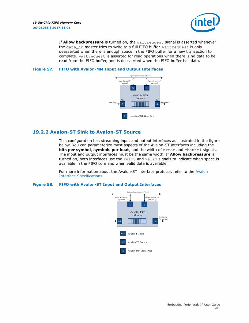
If Allow backpressure is turned on, the waitrequest signal is asserted wheneverthe data_in master tries to write to a full FIFO buffer. waitrequest is onlydeasserted when there is enough space in the FIFO buffer for a new transaction tocomplete. waitrequest is asserted for read operations when there is no data to beread from the FIFO buffer, and is deasserted when the FIFO buffer has data.
Figure 57. FIFO with Avalon-MM Input and Output Interfaces
S Ava lon-MM Slave Po rt
On-Chip FIFOMemory
S S
SS
Wr Rd
Input S ta tus I/F(optiona l)
Output S tatu s I/F(optiona l)
sys tem interconne ct fabric
Input dat a Output dat a
19.2.2 Avalon-ST Sink to Avalon-ST Source
This configuration has streaming input and output interfaces as illustrated in the figurebelow. You can parameterize most aspects of the Avalon-ST interfaces including thebits per symbol, symbols per beat, and the width of error and channel signals.The input and output interfaces must be the same width. If Allow backpressure isturned on, both interfaces use the ready and valid signals to indicate when space isavailable in the FIFO core and when valid data is available.
For more information about the Avalon-ST interface protocol, refer to the AvalonInterface Specifications.
Figure 58. FIFO with Avalon-ST Input and Output Interfaces
SNK Ava lon-ST Sink
On-Chip FIFOMemory
S S
SNK SRC
Input Statu s I/F(opt iona l)
Output Statu s I/F(optiona l)
Sys tem Interconn ect Fab ric
St reamingOutput Dat a
SRC Ava lon-ST Sou rce
S Avalon-MM Slave Port
19 On-Chip FIFO Memory Core
UG-01085 | 2017.11.06
Embedded Peripherals IP User Guide201
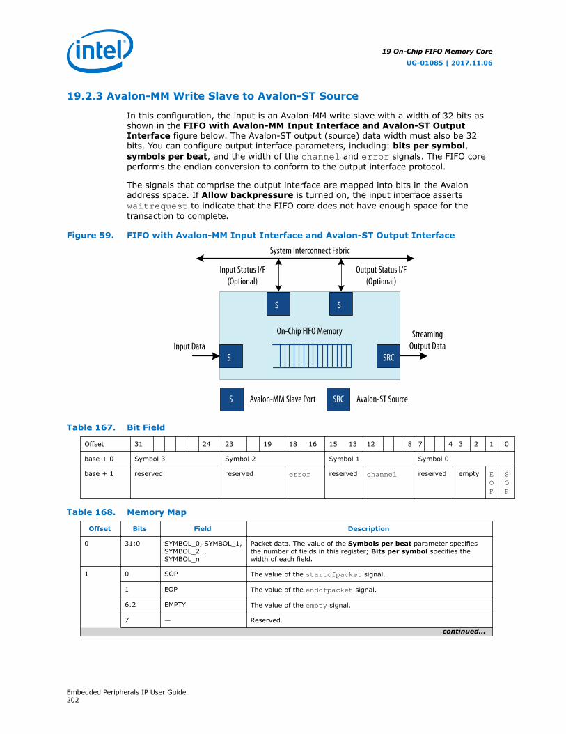
19.2.3 Avalon-MM Write Slave to Avalon-ST Source
In this configuration, the input is an Avalon-MM write slave with a width of 32 bits asshown in the FIFO with Avalon-MM Input Interface and Avalon-ST OutputInterface figure below. The Avalon-ST output (source) data width must also be 32bits. You can configure output interface parameters, including: bits per symbol,symbols per beat, and the width of the channel and error signals. The FIFO coreperforms the endian conversion to conform to the output interface protocol.
The signals that comprise the output interface are mapped into bits in the Avalonaddress space. If Allow backpressure is turned on, the input interface assertswaitrequest to indicate that the FIFO core does not have enough space for thetransaction to complete.
Figure 59. FIFO with Avalon-MM Input Interface and Avalon-ST Output Interface
S S
S
S
System Interconnect Fabric
Input Status I/F(Optional)
Output Status I/F(Optional)
StreamingOutput DataInput Data
On-Chip FIFO Memory
Avalon-MM Slave Port Avalon-ST Source
SRC
SRC
Table 167. Bit Field
Offset 31 24 23 19 18 16 15 13 12 8 7 4 3 2 1 0
base + 0 Symbol 3 Symbol 2 Symbol 1 Symbol 0
base + 1 reserved reserved error reserved channel reserved empty EOP
SOP
Table 168. Memory Map
Offset Bits Field Description
0 31:0 SYMBOL_0, SYMBOL_1,SYMBOL_2 ..SYMBOL_n
Packet data. The value of the Symbols per beat parameter specifiesthe number of fields in this register; Bits per symbol specifies thewidth of each field.
1 0 SOP The value of the startofpacket signal.
1 EOP The value of the endofpacket signal.
6:2 EMPTY The value of the empty signal.
7 — Reserved.
continued...
19 On-Chip FIFO Memory Core
UG-01085 | 2017.11.06
Embedded Peripherals IP User Guide202

Offset Bits Field Description
15:8 CHANNEL The value of the channel signal. The number of bits occupiedcorresponds to the width of the signal. For example, if the width of thechannel signal is 5, bits 8 to 12 are occupied and bits 13 to 15 areunused.
23:16 ERROR The value of the error signal. The number of bits occupied correspondsto the width of the signal. For example, if the width of the error signal is3, bits 16 to 18 are occupied and bits 19 to 23 are unused.
31:24 — Reserved.
If Enable packet data is turned off, the Avalon-MM write master writes all data ataddress offset 0 repeatedly to push data into the FIFO core.
If Enable packet data is turned on, the Avalon-MM write master starts by writing theSOP, ERROR (optional), CHANNEL (optional), EOP, and EMPTY packet statusinformation at address offset 1. Writing to address offset 1 does not push data into theFIFO core. The Avalon-MM master then writes packet data to address offset 0repeatedly, pushing 8-bit symbols into the FIFO core. Whenever a valid write occurs ataddress offset 0, the data and its respective packet information is pushed into theFIFO core. Subsequent data is written at address offset 0 without the need to clear theSOP field. Rewriting to address offset 1 is not required each time if the subsequentdata to be pushed into the FIFO core is not the end-of-packet data, as long as ERRORand CHANNEL do not change.
At the end of each packet, the Avalon-MM master writes to the address at offset 1 toset the EOP bit to 1, before writing the last symbol of the packet at offset 0. The writemaster uses the empty field to indicate the number of unused symbols at the end ofthe transfer. If the last packet data is not aligned with the symbols per beat, theEMPTY field indicates the number of empty symbols in the last packet data. Forexample, if the Avalon-ST interface has symbols per beat of 4, and the last packetonly has 3 symbols, the empty field will be 1, indicating that one symbol (the leastsignificant symbol in the memory map) is empty.
19.2.4 Avalon-ST Sink to Avalon-MM Read Slave
In this configuration seen in the figure below, the input is an Avalon-ST sink and theoutput is an Avalon-MM read slave with a width of 32 bits. The Avalon-ST input (sink)data width must also be 32 bits. You can configure input interface parameters,including: bits per symbol, symbols per beat, and the width of the channel anderror signals. The FIFO core performs the endian conversion to conform to theoutput interface protocol.
An Avalon-MM master reads the data from the FIFO core. The signals are mapped intobits in the Avalon address space. If Allow backpressure is turned on, the input(sink) interface uses the ready and valid signals to indicate when space is availablein the FIFO core and when valid data is available. For the output interface,waitrequest is asserted for read operations when there is no data to be read fromthe FIFO core. It is deasserted when the FIFO core has data to send. The memorymap for this configuration is exactly the same as for the Avalon-MM to Avalon-ST FIFOcore. See the for Memory Map table for more information.
19 On-Chip FIFO Memory Core
UG-01085 | 2017.11.06
Embedded Peripherals IP User Guide203
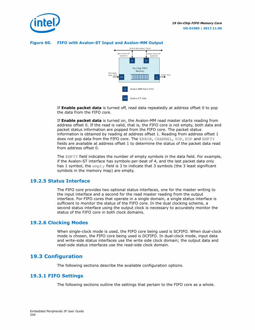
Figure 60. FIFO with Avalon-ST Input and Avalon-MM Output
On-Chip FIFOMemory
S S
SNK S
Inpu t Sta tus I/F(optiona l)
Output Sta tus I/F(optiona l)
Syste m Interconnect Fab ric
Output DataStrea mingInput Data
SNK Avalo n-ST Sink
S Avalon-MM Slave Port
If Enable packet data is turned off, read data repeatedly at address offset 0 to popthe data from the FIFO core.
If Enable packet data is turned on, the Avalon-MM read master starts reading fromaddress offset 0. If the read is valid, that is, the FIFO core is not empty, both data andpacket status information are popped from the FIFO core. The packet statusinformation is obtained by reading at address offset 1. Reading from address offset 1does not pop data from the FIFO core. The ERROR, CHANNEL, SOP, EOP and EMPTYfields are available at address offset 1 to determine the status of the packet data readfrom address offset 0.
The EMPTY field indicates the number of empty symbols in the data field. For example,if the Avalon-ST interface has symbols-per-beat of 4, and the last packet data onlyhas 1 symbol, the empty field is 3 to indicate that 3 symbols (the 3 least significantsymbols in the memory map) are empty.
19.2.5 Status Interface
The FIFO core provides two optional status interfaces, one for the master writing tothe input interface and a second for the read master reading from the outputinterface. For FIFO cores that operate in a single domain, a single status interface issufficient to monitor the status of the FIFO core. In the dual clocking scheme, asecond status interface using the output clock is necessary to accurately monitor thestatus of the FIFO core in both clock domains.
19.2.6 Clocking Modes
When single-clock mode is used, the FIFO core being used is SCFIFO. When dual-clockmode is chosen, the FIFO core being used is DCFIFO. In dual-clock mode, input dataand write-side status interfaces use the write side clock domain; the output data andread-side status interfaces use the read-side clock domain.
19.3 Configuration
The following sections describe the available configuration options.
19.3.1 FIFO Settings
The following sections outline the settings that pertain to the FIFO core as a whole.
19 On-Chip FIFO Memory Core
UG-01085 | 2017.11.06
Embedded Peripherals IP User Guide204
Depth
Depth indicates the depth of the FIFO buffer, in Avalon-ST bits or Avalon-MM words.The default depth is 16. When dual clock mode is used, the actual FIFO depth is equalto depth-3. This is due to clock crossing and to avoid FIFO overflow.
Clock Settings
The two options are Single clock mode and Dual clock mode. In Single clockmode, all interface ports use the same clock. In Dual clock mode, input data andinput side status are on the input clock domain. Output data and output side statusare on the output clock domain.
Status Port
The optional status ports are Avalon-MM slaves. To include the optional input sidestatus interface, turn on Create status interface for input on the Platform DesignerMegaWizard. For FIFOs whose input and output ports operate in separate clockdomains, you can include a second status interface by turning on Create statusinterface for output. Turning on Enable IRQ for status ports adds an interruptsignal to the status ports.
FIFO Implementation
This option determines if the FIFO core is built from registers or embedded memoryblocks. The default is to construct the FIFO core from embedded memory blocks.
19.3.2 Interface Parameters
The following sections outline the options for the input and output interfaces.
Input
Available input interfaces are Avalon-MM write slave and Avalon-ST sink.
Output
Available output interfaces are Avalon-MM read slave and Avalon-ST source.
Allow Backpressure
When Allow backpressure is on, an Avalon-MM interface includes the waitrequestsignal which is asserted to prevent a master from writing to a full FIFO buffer orreading from an empty FIFO buffer. An Avalon-ST interface includes the ready andvalid signals to prevent underflow and overflow conditions.
Avalon-MM Port Settings
Valid Data widths are 8, 16, and 32 bits.
If Avalon-MM is selected for one interface and Avalon-ST for the other, the data widthis fixed at 32 bits.
The Avalon-MM interface accesses data 4 bytes at a time. For data widths other than32 bits, be careful of potential overflow and underflow conditions.
19 On-Chip FIFO Memory Core
UG-01085 | 2017.11.06
Embedded Peripherals IP User Guide205
Avalon-ST Port Settings
The following parameters allow you to specify the size and error handling of theAvalon-ST port or ports:
• Bits per symbol
• Symbols per beat
• Channel width
• Error width
If the symbol size is not a power of two, it is rounded up to the next power of two.For example, if the bits per symbol is 10, the symbol will be mapped to a 16-bitmemory location. With 10-bit symbols, the maximum number of symbols perbeat is two.
Enable packet data provides an option for packet transmission.
19.4 Software Programming Model
The following sections describe the software programming model for the on-chip FIFOmemory core, including the register map and software declarations to access thehardware. For Nios II processor users, Intel provides HAL system library drivers thatenable you to access the on-chip FIFO memory core using its HAL API.
19.4.1 HAL System Library Support
The Intel-provided driver implements a HAL device driver that integrates into the HALsystem library for Nios II systems. HAL users should access the on-chip FIFO memoryvia the familiar HAL API, rather than accessing the registers directly.
19.4.2 Software Files
Intel provides the following software files for the on-chip FIFO memory core:
• altera_avalon_fifo_regs.h—This file defines the core's register map,providing symbolic constants to access the low-level hardware.
• altera_avalon_fifo_util.h—This file defines functions to access the on-chipFIFO memory core hardware. It provides utilities to initialize the FIFO, read andwrite status, enable flags and read events.
• altera_avalon_fifo.h—This file provides the public interface to the on-chipFIFO memory
• altera_avalon_fifo_util.c—This file implements the utilities listed inaltera_avalon_fifo_util.h.
19.5 Programming with the On-Chip FIFO Memory
This section describes the low-level software constructs for manipulating the on-chipFIFO memory core hardware. The table below lists all of the available functions.
19 On-Chip FIFO Memory Core
UG-01085 | 2017.11.06
Embedded Peripherals IP User Guide206
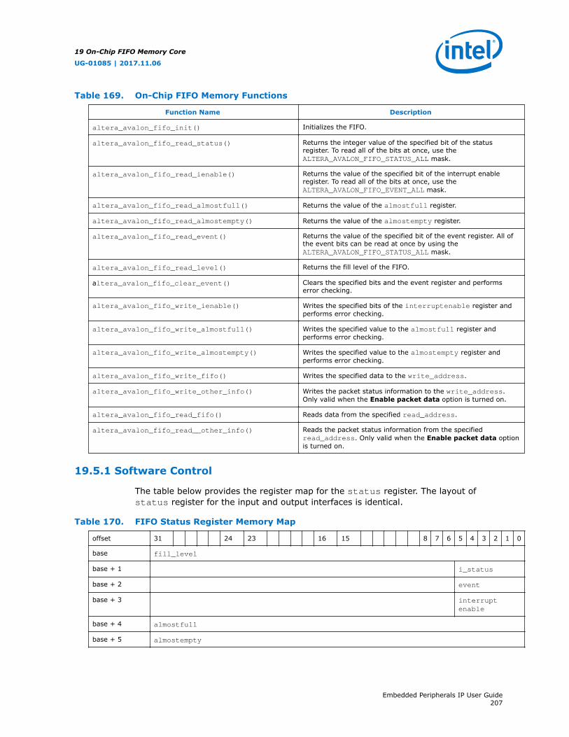
Table 169. On-Chip FIFO Memory Functions
Function Name Description
altera_avalon_fifo_init() Initializes the FIFO.
altera_avalon_fifo_read_status() Returns the integer value of the specified bit of the statusregister. To read all of the bits at once, use theALTERA_AVALON_FIFO_STATUS_ALL mask.
altera_avalon_fifo_read_ienable() Returns the value of the specified bit of the interrupt enableregister. To read all of the bits at once, use theALTERA_AVALON_FIFO_EVENT_ALL mask.
altera_avalon_fifo_read_almostfull() Returns the value of the almostfull register.
altera_avalon_fifo_read_almostempty() Returns the value of the almostempty register.
altera_avalon_fifo_read_event() Returns the value of the specified bit of the event register. All ofthe event bits can be read at once by using theALTERA_AVALON_FIFO_STATUS_ALL mask.
altera_avalon_fifo_read_level() Returns the fill level of the FIFO.
altera_avalon_fifo_clear_event() Clears the specified bits and the event register and performserror checking.
altera_avalon_fifo_write_ienable() Writes the specified bits of the interruptenable register andperforms error checking.
altera_avalon_fifo_write_almostfull() Writes the specified value to the almostfull register andperforms error checking.
altera_avalon_fifo_write_almostempty() Writes the specified value to the almostempty register andperforms error checking.
altera_avalon_fifo_write_fifo() Writes the specified data to the write_address.
altera_avalon_fifo_write_other_info() Writes the packet status information to the write_address.Only valid when the Enable packet data option is turned on.
altera_avalon_fifo_read_fifo() Reads data from the specified read_address.
altera_avalon_fifo_read__other_info() Reads the packet status information from the specifiedread_address. Only valid when the Enable packet data optionis turned on.
19.5.1 Software Control
The table below provides the register map for the status register. The layout ofstatus register for the input and output interfaces is identical.
Table 170. FIFO Status Register Memory Map
offset 31 24 23 16 15 8 7 6 5 4 3 2 1 0
base fill_level
base + 1 i_status
base + 2 event
base + 3 interruptenable
base + 4 almostfull
base + 5 almostempty
19 On-Chip FIFO Memory Core
UG-01085 | 2017.11.06
Embedded Peripherals IP User Guide207
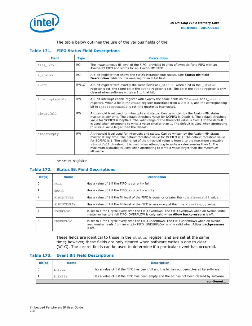
The table below outlines the use of the various fields of the
Table 171. FIFO Status Field Descriptions
Field Type Description
fill_level RO The instantaneous fill level of the FIFO, provided in units of symbols for a FIFO with anAvalon-ST FIFO and words for an Avalon-MM FIFO.
i_status RO A 6-bit register that shows the FIFO’s instantaneous status. See Status Bit FieldDescription Table for the meaning of each bit field.
event RW1C A 6-bit register with exactly the same fields as i_status. When a bit in the i_statusregister is set, the same bit in the event register is set. The bit in the event register is onlycleared when software writes a 1 to that bit.
interruptenable RW A 6-bit interrupt enable register with exactly the same fields as the event and i_statusregisters. When a bit in the event register transitions from a 0 to a 1, and the correspondingbit in interruptenable is set, the master Is interrupted.
almostfull RW A threshold level used for interrupts and status. Can be written by the Avalon-MM statusmaster at any time. The default threshold value for DCFIFO is Depth-4. The default thresholdvalue for SCFIFO is Depth-1. The valid range of the threshold value is from 1 to the default. 1is used when attempting to write a value smaller than 1. The default is used when attemptingto write a value larger than the default.
almostempty RW A threshold level used for interrupts and status. Can be written by the Avalon-MM statusmaster at any time. The default threshold value for DCFIFO is 1. The default threshold valuefor SCFIFO is 1. The valid range of the threshold value is from 1 to the maximum allowablealmostfull threshold. 1 is used when attempting to write a value smaller than 1. Themaximum allowable is used when attempting to write a value larger than the maximumallowable.
status register.
Table 172. Status Bit Field Descriptions
Bit(s) Name Description
0 FULL Has a value of 1 if the FIFO is currently full.
1 EMPTY Has a value of 1 if the FIFO is currently empty.
2 ALMOSTFULL Has a value of 1 if the fill level of the FIFO is equal or greater than the almostfull value.
3 ALMOSTEMPTY Has a value of 1 if the fill level of the FIFO is less or equal than the almostempty value.
4 OVERFLOW Is set to 1 for 1 cycle every time the FIFO overflows. The FIFO overflows when an Avalon writemaster writes to a full FIFO. OVERFLOW is only valid when Allow backpressure is off.
5 UNDERFLOW Is set to 1 for 1 cycle every time the FIFO underflows. The FIFO underflows when an Avalonread master reads from an empty FIFO. UNDERFLOW is only valid when Allow backpressureis off.
These fields are identical to those in the status register and are set at the sametime; however, these fields are only cleared when software writes a one to clear(W1C). The event fields can be used to determine if a particular event has occurred.
Table 173. Event Bit Field Descriptions
Bit(s) Name Description
0 E_FULL Has a value of 1 if the FIFO has been full and the bit has not been cleared by software.
1 E_EMPTY Has a value of 1 if the FIFO has been empty and the bit has not been cleared by software.
continued...
19 On-Chip FIFO Memory Core
UG-01085 | 2017.11.06
Embedded Peripherals IP User Guide208
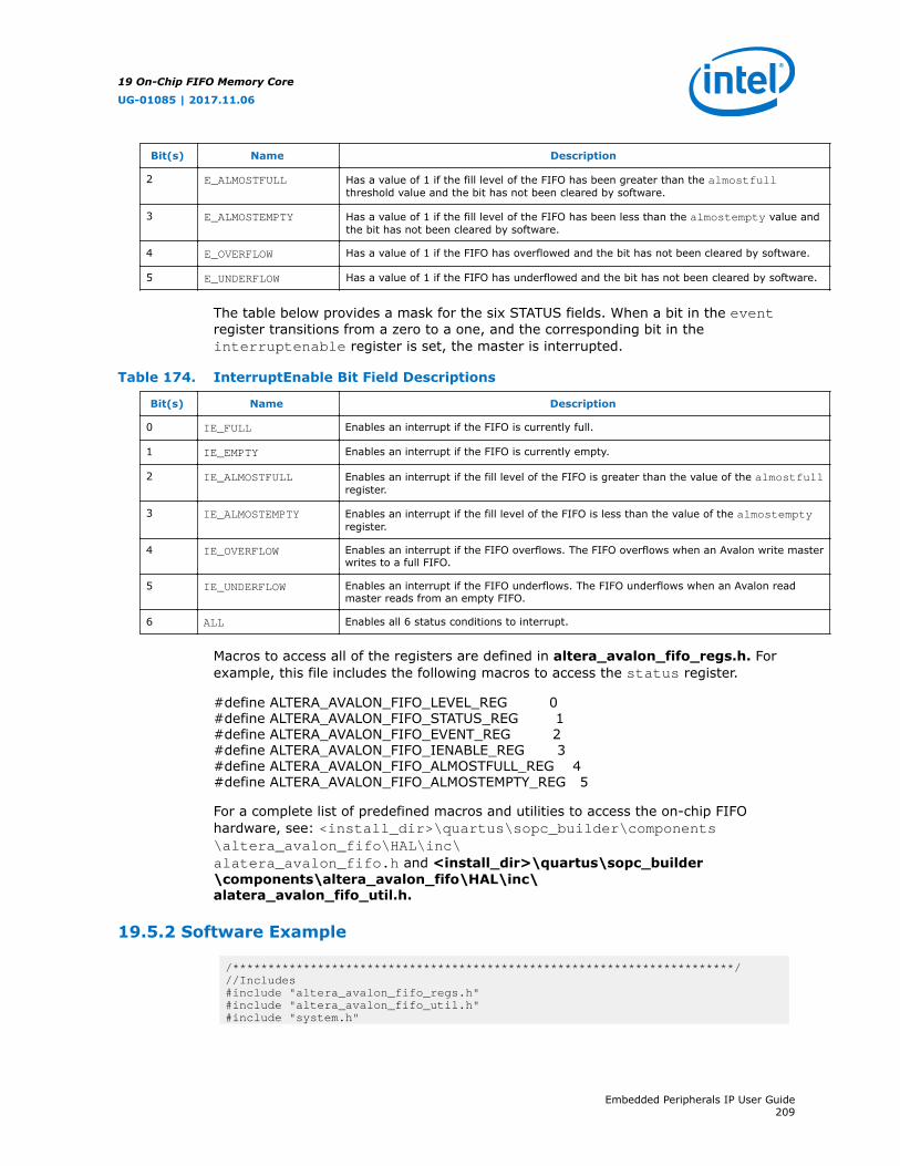
Bit(s) Name Description
2 E_ALMOSTFULL Has a value of 1 if the fill level of the FIFO has been greater than the almostfullthreshold value and the bit has not been cleared by software.
3 E_ALMOSTEMPTY Has a value of 1 if the fill level of the FIFO has been less than the almostempty value andthe bit has not been cleared by software.
4 E_OVERFLOW Has a value of 1 if the FIFO has overflowed and the bit has not been cleared by software.
5 E_UNDERFLOW Has a value of 1 if the FIFO has underflowed and the bit has not been cleared by software.
The table below provides a mask for the six STATUS fields. When a bit in the eventregister transitions from a zero to a one, and the corresponding bit in theinterruptenable register is set, the master is interrupted.
Table 174. InterruptEnable Bit Field Descriptions
Bit(s) Name Description
0 IE_FULL Enables an interrupt if the FIFO is currently full.
1 IE_EMPTY Enables an interrupt if the FIFO is currently empty.
2 IE_ALMOSTFULL Enables an interrupt if the fill level of the FIFO is greater than the value of the almostfullregister.
3 IE_ALMOSTEMPTY Enables an interrupt if the fill level of the FIFO is less than the value of the almostemptyregister.
4 IE_OVERFLOW Enables an interrupt if the FIFO overflows. The FIFO overflows when an Avalon write masterwrites to a full FIFO.
5 IE_UNDERFLOW Enables an interrupt if the FIFO underflows. The FIFO underflows when an Avalon readmaster reads from an empty FIFO.
6 ALL Enables all 6 status conditions to interrupt.
Macros to access all of the registers are defined in altera_avalon_fifo_regs.h. Forexample, this file includes the following macros to access the status register.
#define ALTERA_AVALON_FIFO_LEVEL_REG 0#define ALTERA_AVALON_FIFO_STATUS_REG 1#define ALTERA_AVALON_FIFO_EVENT_REG 2#define ALTERA_AVALON_FIFO_IENABLE_REG 3#define ALTERA_AVALON_FIFO_ALMOSTFULL_REG 4#define ALTERA_AVALON_FIFO_ALMOSTEMPTY_REG 5
For a complete list of predefined macros and utilities to access the on-chip FIFOhardware, see: <install_dir>\quartus\sopc_builder\components\altera_avalon_fifo\HAL\inc\alatera_avalon_fifo.h and <install_dir>\quartus\sopc_builder\components\altera_avalon_fifo\HAL\inc\alatera_avalon_fifo_util.h.
19.5.2 Software Example
/***********************************************************************///Includes#include "altera_avalon_fifo_regs.h"#include "altera_avalon_fifo_util.h"#include "system.h"
19 On-Chip FIFO Memory Core
UG-01085 | 2017.11.06
Embedded Peripherals IP User Guide209
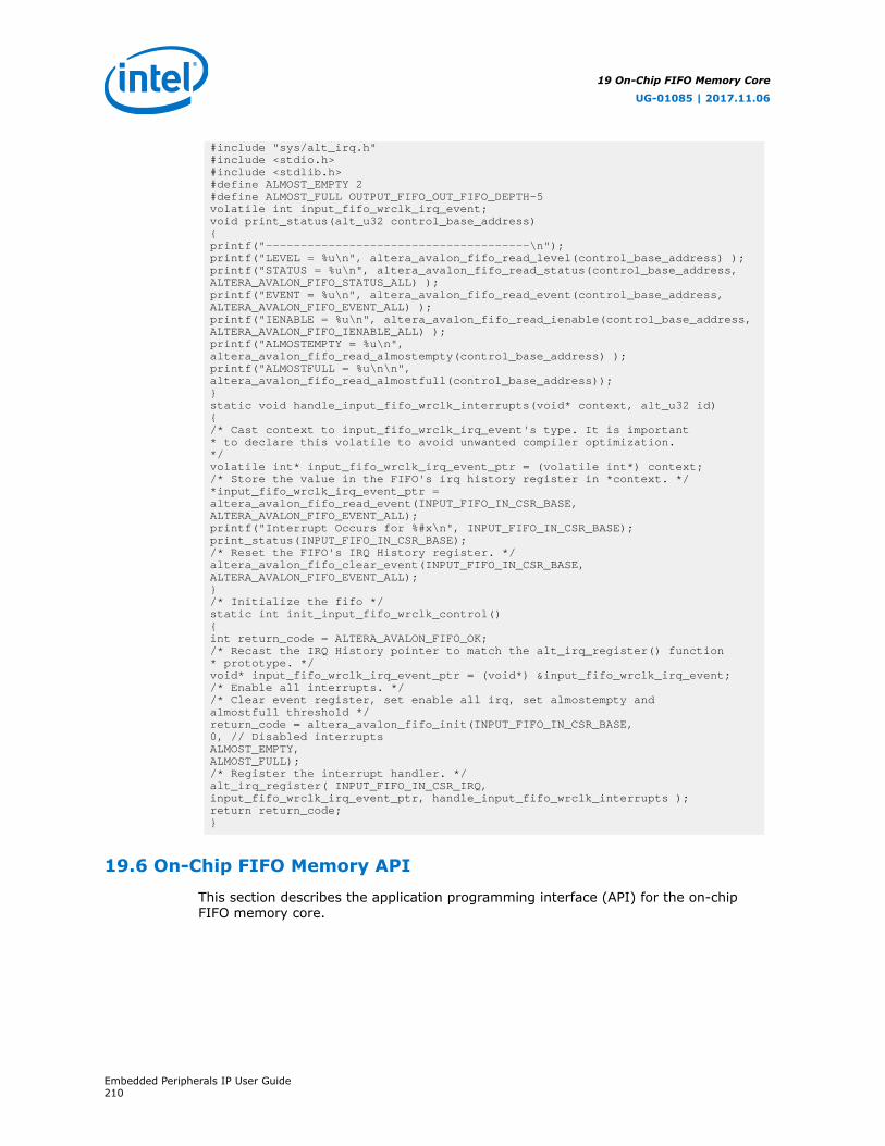
#include "sys/alt_irq.h"#include <stdio.h>#include <stdlib.h>#define ALMOST_EMPTY 2#define ALMOST_FULL OUTPUT_FIFO_OUT_FIFO_DEPTH-5volatile int input_fifo_wrclk_irq_event;void print_status(alt_u32 control_base_address){printf("--------------------------------------\n");printf("LEVEL = %u\n", altera_avalon_fifo_read_level(control_base_address) );printf("STATUS = %u\n", altera_avalon_fifo_read_status(control_base_address,ALTERA_AVALON_FIFO_STATUS_ALL) );printf("EVENT = %u\n", altera_avalon_fifo_read_event(control_base_address,ALTERA_AVALON_FIFO_EVENT_ALL) );printf("IENABLE = %u\n", altera_avalon_fifo_read_ienable(control_base_address,ALTERA_AVALON_FIFO_IENABLE_ALL) );printf("ALMOSTEMPTY = %u\n",altera_avalon_fifo_read_almostempty(control_base_address) );printf("ALMOSTFULL = %u\n\n",altera_avalon_fifo_read_almostfull(control_base_address));}static void handle_input_fifo_wrclk_interrupts(void* context, alt_u32 id){/* Cast context to input_fifo_wrclk_irq_event's type. It is important* to declare this volatile to avoid unwanted compiler optimization.*/volatile int* input_fifo_wrclk_irq_event_ptr = (volatile int*) context;/* Store the value in the FIFO's irq history register in *context. */*input_fifo_wrclk_irq_event_ptr =altera_avalon_fifo_read_event(INPUT_FIFO_IN_CSR_BASE, ALTERA_AVALON_FIFO_EVENT_ALL);printf("Interrupt Occurs for %#x\n", INPUT_FIFO_IN_CSR_BASE);print_status(INPUT_FIFO_IN_CSR_BASE);/* Reset the FIFO's IRQ History register. */altera_avalon_fifo_clear_event(INPUT_FIFO_IN_CSR_BASE,ALTERA_AVALON_FIFO_EVENT_ALL);}/* Initialize the fifo */static int init_input_fifo_wrclk_control(){int return_code = ALTERA_AVALON_FIFO_OK;/* Recast the IRQ History pointer to match the alt_irq_register() function* prototype. */void* input_fifo_wrclk_irq_event_ptr = (void*) &input_fifo_wrclk_irq_event;/* Enable all interrupts. *//* Clear event register, set enable all irq, set almostempty andalmostfull threshold */return_code = altera_avalon_fifo_init(INPUT_FIFO_IN_CSR_BASE,0, // Disabled interruptsALMOST_EMPTY,ALMOST_FULL);/* Register the interrupt handler. */alt_irq_register( INPUT_FIFO_IN_CSR_IRQ,input_fifo_wrclk_irq_event_ptr, handle_input_fifo_wrclk_interrupts );return return_code;}
19.6 On-Chip FIFO Memory API
This section describes the application programming interface (API) for the on-chipFIFO memory core.
19 On-Chip FIFO Memory Core
UG-01085 | 2017.11.06
Embedded Peripherals IP User Guide210
19.6.1 altera_avalon_fifo_init()
Prototype: int altera_avalon_fifo_init(alt_u32 address, alt_u32 ienable, alt_u32emptymark, alt_u32 fullmark)
Thread-safe: No.
Available from ISR: No.
Include: <altera_avalon_fifo_regs.h>, <altera_avalon_fifo_utils.h>
Parameters: address—the base address of the FIFO control slaveienable—the value to write to the interruptenable registeremptymark—the value for the almost empty threshold levelfullmark—the value for the almost full threshold level
Returns: Returns 0 (ALTERA_AVALON_FIFO_OK) if successful, ALTERA_AVALON_FIFO_EVENT_CLEAR_ERRORfor clear errors, ALTERA_AVALON_FIFO_IENABLE_WRITE_ERROR for interrupt enable write errors,ALTERA_AVALON_FIFO_THRESHOLD_WRITE_ERROR for errors writing the almostfull andalmostempty registers.
Description: Clears the event register, writes the interruptenable register, and sets the almostfull registerand almostempty registers.
19.6.2 altera_avalon_fifo_read_status()
Prototype: int altera_avalon_fifo_read_status(alt_u32 address, alt_u32 mask)
Thread-safe: No.
Available from ISR: No.
Include: <altera_avalon_fifo_regs.h>, <altera_avalon_fifo_utils.h>
Parameters: address—the base address of the FIFO control slavemask—masks the read value from the status register
Returns: Returns the masked bits of the addressed register.
Description: Gets the addressed register bits—the AND of the value of the addressed register and the mask.
19.6.3 altera_avalon_fifo_read_ienable()
Prototype: int altera_avalon_fifo_read_ienable(alt_u32 address, alt_u32 mask)
Thread-safe: No.
Available from ISR: No.
Include: <altera_avalon_fifo_regs.h>, <altera_avalon_fifo_utils.h>
Parameters: address—the base address of the FIFO control slavemask—masks the read value from the interruptenable register
Returns: Returns the logical AND of the interruptenable register and the mask.
Description: Gets the logical AND of the interruptenable register and the mask.
19 On-Chip FIFO Memory Core
UG-01085 | 2017.11.06
Embedded Peripherals IP User Guide211

19.6.4 altera_avalon_fifo_read_almostfull()
Prototype: int altera_avalon_fifo_read_almostfull(alt_u32 address)
Thread-safe: No.
Available from ISR: No.
Include: <altera_avalon_fifo_regs.h>, <altera_avalon_fifo_utils.h>
Parameters: address—the base address of the FIFO control slave
Returns: Returns the value of the almostfull register.
Description: Gets the value of the almostfull register.
19.6.5 altera_avalon_fifo_read_almostempty()
Prototype: int altera_avalon_fifo_read_almostempty(alt_u32 address)
Thread-safe: No.
Available from ISR: No.
Include: <altera_avalon_fifo_regs.h>, <altera_avalon_fifo_utils.h>
Parameters: address—the base address of the FIFO control slave
Returns: Returns the value of the almostempty register.
Description: Gets the value of the almostempty register.
19.6.6 altera_avalon_fifo_read_event()
Prototype: int altera_avalon_fifo_read_event(alt_u32 address, alt_u32 mask)
Thread-safe: No.
Available from ISR: No.
Include: <altera_avalon_fifo_regs.h>, <altera_avalon_fifo_utils.h>
Parameters: address—the base address of the FIFO control slavemask—masks the read value from the event register
Returns: Returns the logical AND of the event register and the mask.
Description: Gets the logical AND of the event register and the mask. To read single bits of the event register usethe single bit masks, for example: ALTERA_AVALON_FIFO_FIFO_EVENT_F_MSK. To read the entireevent register use the full mask: ALTERA_AVALON_FIFO_EVENT_ALL.
19.6.7 altera_avalon_fifo_read_level()
Prototype: int altera_avalon_fifo_read_level(alt_u32 address)
Thread-safe: No.
Available from ISR: No.
Include: <altera_avalon_fifo_regs.h>, <altera_avalon_fifo_utils.h>
continued...
19 On-Chip FIFO Memory Core
UG-01085 | 2017.11.06
Embedded Peripherals IP User Guide212

Parameters: address—the base address of the FIFO control slave
Returns: Returns the fill level of the FIFO.
Description: Gets the fill level of the FIFO.
19.6.8 altera_avalon_fifo_clear_event()
Prototype: int altera_avalon_fifo_clear_event(alt_u32 address, alt_u32 mask)
Thread-safe: No.
Available from ISR: No.
Include: <altera_avalon_fifo_regs.h>, <altera_avalon_fifo_utils.h>
Parameters: address—the base address of the FIFO control slavemask—the mask to use for bit-clearing (1 means clear this bit, 0 means do not clear)
Returns: Returns 0 (ALTERA_AVALON_FIFO_OK) if successful, ALTERA_AVALON_FIFO_EVENT_CLEAR_ERROR ifunsuccessful.
Description: Clears the specified bits of the event register.
19.6.9 altera_avalon_fifo_write_ienable()
Prototype: int altera_avalon_fifo_write_ienable(alt_u32 address, alt_u32 mask)
Thread-safe: No.
Available from ISR: No.
Include: <altera_avalon_fifo_regs.h>, <altera_avalon_fifo_utils.h>
Parameters: address—the base address of the FIFO control slavemask—the value to write to the interruptenable register. See altera_avalon_fifo_regs.h forindividual interrupt bit masks.
Returns: Returns 0 (ALTERA_AVALON_FIFO_OK) if successful, ALTERA_AVALON_FIFO_IENABLE_WRITE_ERRORif unsuccessful.
Description: Writes the specified bits of the interruptenable register.
19.6.10 altera_avalon_fifo_write_almostfull()
Prototype: int altera_avalon_fifo_write_almostfull(alt_u32 address, alt_u32 data)
Thread-safe: No.
Available from ISR: No.
Include: <altera_avalon_fifo_regs.h>, <altera_avalon_fifo_utils.h>
Parameters: address—the base address of the FIFO control slavedata—the value for the almost full threshold level
Returns: Returns 0 (ALTERA_AVALON_FIFO_OK) if successful,ALTERA_AVALON_FIFO_THRESHOLD_WRITE_ERROR if unsuccessful.
Description: Writes data to the almostfull register.
19 On-Chip FIFO Memory Core
UG-01085 | 2017.11.06
Embedded Peripherals IP User Guide213

19.6.11 altera_avalon_fifo_write_almostempty()
Prototype: int altera_avalon_fifo_write_almostempty(alt_u32 address, alt_u23 data)
Thread-safe: No.
Available from ISR: No.
Include: <altera_avalon_fifo_regs.h>, <altera_avalon_fifo_utils.h>
Parameters: address—the base address of the FIFO control slavedata—the value for the almost empty threshold level
Returns: Returns 0 (ALTERA_AVALON_FIFO_OK) if successful,ALTERA_AVALON_FIFO_THRESHOLD_WRITE_ERROR if unsuccessful.
Description: Writes data to the almostempty register.
19.6.12 altera_avalon_write_fifo()
Prototype: int altera_avalon_write_fifo(alt_u32 write_address, alt_u32 ctrl_address,alt_u32 data)
Thread-safe: No.
Available from ISR: No.
Include: <altera_avalon_fifo_regs.h>, <altera_avalon_fifo_utils.h>
Parameters: write_address—the base address of the FIFO write slavectrl_address—the base address of the FIFO control slavedata—the value to write to address offset 0 for Avalon-MM to Avalon-ST transfers, the value to write tothe single address available for Avalon-MM to Avalon-MM transfers. See the Avalon InterfaceSpecifications section for the data ordering.
Returns: Returns 0 (ALTERA_AVALON_FIFO_OK) if successful, ALTERA_AVALON_FIFO_FULL if unsuccessful.
Description: Writes data to the specified address if the FIFO is not full.
19.6.13 altera_avalon_write_other_info()
Prototype: int altera_avalon_write_other_info(alt_u32 write_address, alt_u32 ctrl_address,alt_u32 data)
Thread-safe: No.
Available from ISR: No.
Include: <altera_avalon_fifo_regs.h>, <altera_avalon_fifo_utils.h>
Parameters: write_address—the base address of the FIFO write slavectrl_address—the base address of the FIFO control slavedata—the packet status information to write to address offset 1 of the Avalon interface. See theAvalon Interface Specifications section for the ordering of the packet status information.
Returns: Returns 0 (ALTERA_AVALON_FIFO_OK) if successful, ALTERA_AVALON_FIFO_FULL if unsuccessful.
Description: Writes the packet status information to the write_address. Only valid when Enable packet data ison.
19 On-Chip FIFO Memory Core
UG-01085 | 2017.11.06
Embedded Peripherals IP User Guide214

19.6.14 altera_avalon_fifo_read_fifo()
Prototype: int altera_avalon_fifo_read_fifo(alt_u32 read_address, alt_u32 ctrl_address)
Thread-safe: No.
Available from ISR: No.
Include: <altera_avalon_fifo_regs.h>, <altera_avalon_fifo_utils.h>
Parameters: read_address—the base address of the FIFO read slavectrl_address—the base address of the FIFO control slave
Returns: Returns the data from address offset 0, or 0 if the FIFO is empty.
Description: Gets the data addressed by read_address.
R**altera_avalon_fifo_read_other_info()
Prototype: int altera_avalon_fifo_read_other_info(alt_u32 read_address)
Thread-safe: No.
Available from ISR: No.
Include: <altera_avalon_fifo_regs.h>, <altera_avalon_fifo_utils.h>
Parameters: read_address—the base address of the FIFO read slave
Returns: Returns the packet status information from address offset 1 of the Avalon interface. See the AvalonInterface Specifications section for the ordering of the packet status information.
Description: Reads the packet status information from the specified read_address. Only valid when Enablepacket data is on.
19.7 Document Revision History
Table 175. On-Chip FIFO Memory Core Revision History
Date Version Changes
July 2014 2014.07.24 Removed mention of Platform Designer, updated to Platform Designer
December 2010 v10.1.0 Removed the “Device Support”, “Instantiating the Core in PlatformDesigner”, and “Referenced Documents” sections.
July 2010 v10.0.0 Revised the description of the memory map.
November 2009 v9.1.0 Added description to the core overview.
March 2009 v9.0.0 Updated the description of the function altera_avalon_fifo_read_status().
November 2008 v8.1.0 Changed to 8-1/2 x 11 page size. No change to content.
May 2008 v8.0.0 No change from previous release.
19 On-Chip FIFO Memory Core
UG-01085 | 2017.11.06
Embedded Peripherals IP User Guide215

20 On-Chip Memory (RAM and ROM) Core
20.1 Core Overview
Intel FPGAs include on-chip memory blocks that can be used as RAM or ROM inPlatform Designer systems. On-chip memory has the following benefits for PlatformDesigner systems:
• On-chip memory has fast access time, compared to off-chip memory.
• Platform Designer automatically instantiates on-chip memory inside the PlatformDesigner system, so you do not have to make any manual connections.
• Certain memory blocks can have initialized contents when the FPGA powers up.This feature is useful, for example, for storing data constants or processor bootcode.
• On-chip memories support dual port accesses, allowing two master to access thesame memory concurrently.
20.2 Component-Level Design for On-Chip Memory
In Platform Designer you instantiate on-chip memory by clicking On-chip Memory(RAM or ROM) from the list of available components. The configuration window for theOn-chip Memory (RAM or ROM) component has the following options: Memory type,Size, and Read latency.
UG-01085 | 2017.11.06
Intel Corporation. All rights reserved. Intel, the Intel logo, Altera, Arria, Cyclone, Enpirion, MAX, Nios, Quartusand Stratix words and logos are trademarks of Intel Corporation or its subsidiaries in the U.S. and/or othercountries. Intel warrants performance of its FPGA and semiconductor products to current specifications inaccordance with Intel's standard warranty, but reserves the right to make changes to any products and servicesat any time without notice. Intel assumes no responsibility or liability arising out of the application or use of anyinformation, product, or service described herein except as expressly agreed to in writing by Intel. Intelcustomers are advised to obtain the latest version of device specifications before relying on any publishedinformation and before placing orders for products or services.*Other names and brands may be claimed as the property of others.
ISO9001:2008Registered
20.2.1 Memory Type
This options defines the structure of the on-chip memory:
• RAM (writable)—This setting creates a readable and writable memory.
• ROM (read only)—This setting creates a read-only memory.
• Dual-port access—This setting creates a memory component with two slaves,which allows two masters to access the memory simultaneously.
Note: The memory component operates under true dual-port mode where bothslave ports have address ports for read or write operations. If two mastersaccess the same address simultaneously in a dual-port memory undefinedresults will occur. Concurrent accesses are only a problem for two writes. Aread and write to the same location will read out the old data and store thenew data.
• Single clock operation—Single clock operation setting creates single clock sourceto clock both slaves port. If single clock operation is not selected, each of the twoslaves port is clocked by different clock sources.
Note: For Intel Stratix 10 devices, only single clock operation is supported.
• Read During Write Mode—This setting determines what the output data of thememory should be when a simultaneous read and write to the same memorylocation occurs.
• Block type—This setting directs the Intel Quartus Prime software to use a specifictype of memory block when fitting the on-chip memory in the FPGA.
Note: The MRAM blocks do not allow the contents to be initialized during powerup. The M512s memory type does not support dual-port mode where bothports support both reads and writes.
Because of the constraints on some memory types, it is frequently best to use theAuto setting. Auto allows the Intel Quartus Prime software to choose a type and theother settings direct the Intel Quartus Prime software to select a particular type.
20 On-Chip Memory (RAM and ROM) Core
UG-01085 | 2017.11.06
Embedded Peripherals IP User Guide217

20.2.2 Size
This options defines the size and width of the memory.
• Enable different width for Dual-port Access—Different width for dual-port accessstatus.
Note: A different width for dual-port access is not supported for Intel Stratix 10devices.
• Slave S1 Data width—This setting determines the data width of the memory. Theavailable choices are 8, 16, 32, 64, 128, 256, 512, or 1024 bits. Assign Data widthto match the width of the master that accesses this memory the most frequentlyor has the most critical throughput requirements. For example, if you areconnecting the on-chip memory to the data master of a Nios II processor, youshould set the data width of the on-chip memory to 32 bits, the same as the data-width of the Nios II data master. Otherwise, the access latency could be longerthan one cycle because the Avalon interconnect fabric performs width translation.
• Total memory size—This setting determines the total size of the on-chip memoryblock. The total memory size must be less than the available memory in the targetFPGA.
• Minimize memory block usage (may impact fmax)—Minimize memory block usage(may impact fmax)—This option is only available for devices that include M4Kmemory blocks. If selected, the Intel Quartus Prime software divides the memoryby depth rather than width, so that fewer memory blocks are used. This changemay decrease fmax.
20.2.3 Read Latency
On-chip memory components use synchronous, pipelined Avalon-MM slaves. Pipelinedaccess improves fMAX performance, but also adds latency cycles when reading thememory. The Read latency option allows you to specify either one or two cycles ofread latency required to access data. If the Dual-port access setting is turned on, youcan specify a different read latency for each slave. When you have dual-port memoryin your system you can specify different clock frequencies for the ports. You specifythis on the System Contents tab in Platform Designer.
20.2.4 ROM/RAM Memory Protection
This setting if enabled, creates additional reset request port for memory protectionduring reset. This additional reset input port is used to gate off the clock to thememory.
20.2.5 ECC Parameter
This setting if enabled, extends the data width to support ECC bits. It does notinstantiate any ECC encoder or decoder logic within this component.
20 On-Chip Memory (RAM and ROM) Core
UG-01085 | 2017.11.06
Embedded Peripherals IP User Guide218
20.2.6 Memory Initialization
The memory initialization parameter section contains the following options:
• Initialize memory content—Option for user to enable memory contentinitialization.
• Enable non-default initialization file—You can specify your own initialization file byselecting Enable non-default initialization file. This option allows the file youspecify to be used to initialize the memory in place of the default initialization filecreated by Platform Designer.
• Enable Partial Reconfiguartion Initialization Mode—This setting if enabled,automatically instantiates logic to support Partial Reconfiguration use cases forinitialized memory.
• Enable In-System Memory Content Editor Feature—Enables a JTAG interface usedto read and write to the RAM while it is operating. You can use this interface toupdate or read the contents of the memory from your host PC.
20.3 Platform Designer System-Level Design for On-Chip Memory
There are few Platform Designer system-level design considerations for on-chipmemories. See “Platform Designer System-Level Design”.
When generating a new system, Platform Designer creates a blank initialization file inthe Intel Quartus Prime project directory for each on-chip memory that can power upwith initialized contents. The name of this file is <name of memorycomponent>.hex.
20.4 Simulation for On-Chip Memory
At system generation time, Platform Designer generates a simulation model for theon-chip memory. This model is embedded inside the Platform Designer system, andthere are no user-configurable options for the simulation testbench.
You can provide memory initialization contents for simulation in the file <IntelQuartus Prime project directory>/<Platform Designer systemname>_sim/<Memory component name>.hex.
20.5 Intel Quartus Prime Project-Level Design for On-Chip Memory
The on-chip memory is embedded inside the Platform Designer system, and there areno signals to connect to the Intel Quartus Prime project.
To provide memory initialization contents, you must fill in the file <name of memorycomponent>.hex. The Intel Quartus Prime software recognizes this file during designcompilation and incorporates the contents into the configuration files for the FPGA.
Note: For the memory to be initialized, you then must compile the hardware in the IntelQuartus Prime software for the SRAM Object File (.sof) to pick up the memoryinitialization files. All memory types with the exception of MRAMs support this feature.
20 On-Chip Memory (RAM and ROM) Core
UG-01085 | 2017.11.06
Embedded Peripherals IP User Guide219
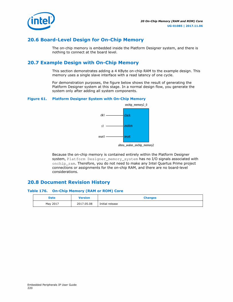
20.6 Board-Level Design for On-Chip Memory
The on-chip memory is embedded inside the Platform Designer system, and there isnothing to connect at the board level.
20.7 Example Design with On-Chip Memory
This section demonstrates adding a 4 KByte on-chip RAM to the example design. Thismemory uses a single slave interface with a read latency of one cycle.
For demonstration purposes, the figure below shows the result of generating thePlatform Designer system at this stage. In a normal design flow, you generate thesystem only after adding all system components.
Figure 61. Platform Designer System with On-Chip Memoryonchip_memory2_0
altera_avalon_onchip_memory2
clk1
s1
reset1
clock
avalon
reset
Because the on-chip memory is contained entirely within the Platform Designersystem, Platform Designer_memory_system has no I/O signals associated withonchip_ram. Therefore, you do not need to make any Intel Quartus Prime projectconnections or assignments for the on-chip RAM, and there are no board-levelconsiderations.
20.8 Document Revision History
Table 176. On-Chip Memory (RAM or ROM) Core
Date Version Changes
May 2017 2017.05.08 Initial release
20 On-Chip Memory (RAM and ROM) Core
UG-01085 | 2017.11.06
Embedded Peripherals IP User Guide220
21 Optrex 16207 LCD Controller Core
21.1 Core Overview
The Optrex 16207 LCD controller core with Avalon Interface (LCD controller core)provides the hardware interface and software driver required for a Nios II processor todisplay characters on an Optrex 16207 (or equivalent) 16×2-character LCD panel.Device drivers are provided in the HAL system library for the Nios II processor. Nios IIprograms access the LCD controller as a character mode device using ANSI C standardlibrary routines, such as printf(). The LCD controller is Platform Designer-ready,and integrates easily into any Platform Designer-generated system.
The Nios II Embedded Design Suite (EDS) includes an Optrex LCD module and provideseveral ready-made example designs that display text on the Optrex 16207 via theLCD controller.
For details about the Optrex 16207 LCD module, see the manufacturer's Dot MatrixCharacter LCD Module User's Manual available online.
21.2 Functional Description
The LCD controller core consists of two user-visible components:
• Eleven signals that connect to pins on the Optrex 16207 LCD panel—These signalsare defined in the Optrex 16207 data sheet.
— E—Enable (output)
— RS—Register Select (output)
— R/W—Read or Write (output)
— DB0 through DB7—Data Bus (bidirectional)
• An Avalon Memory-Mapped (Avalon-MM) slave interface that provides access to 4registers.
UG-01085 | 2017.11.06
Intel Corporation. All rights reserved. Intel, the Intel logo, Altera, Arria, Cyclone, Enpirion, MAX, Nios, Quartusand Stratix words and logos are trademarks of Intel Corporation or its subsidiaries in the U.S. and/or othercountries. Intel warrants performance of its FPGA and semiconductor products to current specifications inaccordance with Intel's standard warranty, but reserves the right to make changes to any products and servicesat any time without notice. Intel assumes no responsibility or liability arising out of the application or use of anyinformation, product, or service described herein except as expressly agreed to in writing by Intel. Intelcustomers are advised to obtain the latest version of device specifications before relying on any publishedinformation and before placing orders for products or services.*Other names and brands may be claimed as the property of others.
ISO9001:2008Registered

Figure 62. LCD Controller Block Diagram
address
data
controlDB0 . . DB7
R/W
RS
E
LCDController
Intel FPGA
Avalon-MM SlaveInterface to
On-Chip Logic
Optrex 16207LCD Module
21.3 Software Programming Model
This section describes the software programming model for the LCD controller.
21.3.1 HAL System Library Support
Intel provides HAL system library drivers for the Nios II processor that enable you toaccess the LCD controller using the ANSI C standard library functions. The Intel-provided drivers integrate into the HAL system library for Nios II systems. The LCDdriver is a standard character-mode device, as described in the Nios II SoftwareDeveloper’s Handbook. Therefore, using printf() is the easiest way to writecharacters to the display.
The LCD driver requires that the HAL system library include the system clock driver.
21.3.2 Displaying Characters on the LCD
The driver implements VT100 terminal-like behavior on a miniature scale for the 16×2screen. Characters written to the LCD controller are stored to an 80-column × 2-rowbuffer maintained by the driver. As characters are written, the cursor position isupdated. Visible characters move the cursor position to the right. Any visiblecharacters written to the right of the buffer are discarded. The line feed character (\n)moves the cursor down one line and to the left-most column.
The buffer is scrolled up as soon as a printable character is written onto the line belowthe bottom of the buffer. Rows do not scroll as soon as the cursor moves down toallow the maximum useful information in the buffer to be displayed.
If the visible characters in the buffer fit on the display, all characters are displayed. Ifthe buffer is wider than the display, the display scrolls horizontally to display all thecharacters. Different lines scroll at different speeds, depending on the number ofcharacters in each line of the buffer.
The LCD driver supports a small subset of ANSI and VT100 escape sequences that canbe used to control the cursor position, and clear the display as shown below.
21 Optrex 16207 LCD Controller Core
UG-01085 | 2017.11.06
Embedded Peripherals IP User Guide222

Table 177. Escape Sequence Supported by the LCD Controller
Sequence Meaning
BS (\b) Moves the cursor to the left by one character.
CR (\r) Moves the cursor to the start of the current line.
LF (\n) Moves the cursor to the start of the line and move it downone line.
ESC ( (\x1B) Starts a VT100 control sequence.
ESC [ <y> ; <x> H Moves the cursor to the y, x position specified – positionsare counted from the top left which is 1;1.
ESC [ K Clears from current cursor position to end of line.
ESC [ 2 J Clears the whole screen.
The LCD controller is an output-only device. Therefore, attempts to read from itreturns immediately indicating that no characters have been received.
The LCD controller drivers are not included in the system library when the Reduceddevice drivers option is enabled for the system library. If you want to use the LCDcontroller while using small drivers for other devices, add the preprocessor option—DALT_USE_LCD_16207 to the preprocessor options.
21.3.3 Software Files
The LCD controller is accompanied by the following software files. These files definethe low-level interface to the hardware and provide the HAL drivers. Applicationdevelopers should not modify these files.
• altera_avalon_lcd_16207_regs.h — This file defines the core's registermap, providing symbolic constants to access the low-level hardware.
• altera_avalon_lcd_16207.h, altera_avalon_lcd_16207.c — These filesimplement the LCD controller device drivers for the HAL system library.
21.3.4 Register Map
The HAL device drivers make it unnecessary for you to access the registers directly.Therefore, Intel does not publish details about the register map. For more information,the altera_avalon_lcd_16207_regs.h file describes the register map, and theDot Matrix Character LCD Module User's Manual from Optrex describes the registerusage.
21.3.5 Interrupt Behavior
The LCD controller does not generate interrupts. However, the LCD driver's textscrolling feature relies on the HAL system clock driver, which uses interrupts for timingpurposes.
21 Optrex 16207 LCD Controller Core
UG-01085 | 2017.11.06
Embedded Peripherals IP User Guide223
21.4 Document Revision History
Table 178. Optrex 16207 LCD Controller Core Revision History
Date Version Changes
July 2014 2014.07.24 Removed mention of SOPC Builder, updated to Platform Designer
December 2010 v10.1.0 Removed the “Device Support”, “Instantiating the Core in SOPC Builder”,and “Referenced Documents” sections.
July 2010 v10.0.0 No change from previous release.
November 2009 v9.1.0 No change from previous release.
March 2009 v9.0.0 No change from previous release.
November 2008 v8.1.0 Changed to 8-1/2 x 11 page size. No change to content.
May 2008 v8.0.0 No change from previous release.
21 Optrex 16207 LCD Controller Core
UG-01085 | 2017.11.06
Embedded Peripherals IP User Guide224

22 PIO Core
22.1 Core Overview
The parallel input/output (PIO) core with Avalon interface provides a memory-mappedinterface between an Avalon Memory-Mapped (Avalon-MM) slave port and general-purpose I/O ports. The I/O ports connect either to on-chip user logic, or to I/O pinsthat connect to devices external to the FPGA.
The PIO core provides easy I/O access to user logic or external devices in situationswhere a “bit banging” approach is sufficient. Some example uses are:
• Controlling LEDs
• Acquiring data from switches
• Controlling display devices
• Configuring and communicating with off-chip devices, such as application-specificstandard products (ASSP)
The PIO core interrupt request (IRQ) output can assert an interrupt based on inputsignals.
22.2 Functional Description
Each PIO core can provide up to 32 I/O ports. An intelligent host such as amicroprocessor controls the PIO ports by reading and writing the register-mappedAvalon-MM interface. Under control of the host, the PIO core captures data on itsinputs and drives data to its outputs. When the PIO ports are connected directly to I/Opins, the host can tristate the pins by writing control registers in the PIO core. Theexample below shows a processor-based system that uses multiple PIO cores to driveLEDs, capture edges from on-chip reset-request control logic, and control an off-chipLCD display.
UG-01085 | 2017.11.06
Intel Corporation. All rights reserved. Intel, the Intel logo, Altera, Arria, Cyclone, Enpirion, MAX, Nios, Quartusand Stratix words and logos are trademarks of Intel Corporation or its subsidiaries in the U.S. and/or othercountries. Intel warrants performance of its FPGA and semiconductor products to current specifications inaccordance with Intel's standard warranty, but reserves the right to make changes to any products and servicesat any time without notice. Intel assumes no responsibility or liability arising out of the application or use of anyinformation, product, or service described herein except as expressly agreed to in writing by Intel. Intelcustomers are advised to obtain the latest version of device specifications before relying on any publishedinformation and before placing orders for products or services.*Other names and brands may be claimed as the property of others.
ISO9001:2008Registered

Figure 63. System Using Multiple PIO Cores
System Interconnect
Fabric
CPU
PIO core(output only)
Program and DataMemory PIO
core (bidirectional)
IRQ
LEDs
EdgeCapture
PIOcore
(input only)
Resetrequest
logic
Intel FPGA
4
11 LCD display
When integrated into an Platform Designer-generated system, the PIO core has twouser-visible features:
• A memory-mapped register space with four registers: data, direction,interruptmask, and edgecapture
• 1 to 32 I/O ports
The I/O ports can be connected to logic inside the FPGA, or to device pins thatconnect to off-chip devices. The registers provide an interface to the I/O ports viathe Avalon-MM interface. See Register Map for the PIO Core table for adescription of the registers.
22.2.1 Data Input and Output
The PIO core I/O ports can connect to either on-chip or off-chip logic. The core can beconfigured with inputs only, outputs only, or both inputs and outputs. If the core isused to control bidirectional I/O pins on the device, the core provides a bidirectionalmode with tristate control.
The hardware logic is separate for reading and writing the data register. Reading thedata register returns the value present on the input ports (if present). Writing dataaffects the value driven to the output ports (if present). These ports are independent;reading the data register does not return previously-written data.
22.2.2 Edge Capture
The PIO core can be configured to capture edges on its input ports. It can capture low-to-high transitions, high-to-low transitions, or both. Whenever an input detects anedge, the condition is indicated in the edgecapture register. The types of edgesdetected is specified at system generation time, and cannot be changed via theregisters.
22.2.3 IRQ Generation
The PIO core can be configured to generate an IRQ on certain input conditions. TheIRQ conditions can be either:
22 PIO Core
UG-01085 | 2017.11.06
Embedded Peripherals IP User Guide226

• Level-sensitive—The PIO core hardware can detect a high level. A NOT gate can beinserted external to the core to provide negative sensitivity.
• Edge-sensitive—The core's edge capture configuration determines which type ofedge causes an IRQ
Interrupts are individually maskable for each input port. The interrupt maskdetermines which input port can generate interrupts.
22.3 Example Configurations
Figure 64. PIO Core with Input Ports, Output Ports, and IRQ Support
datain
out
address
data
control
IRQ
32
inter ruptmask
edgecapture
Avalon-MMinter face
to on-chiplogic
The block diagram below shows the PIO core configured in bidirectional mode, withoutsupport for IRQs.
Figure 65. PIO Cores with Bidirectional Ports
direction
datain
out
address
data
control
32Avalon-MM
Interfaceto On-Chip
Logic
22.3.1 Avalon-MM Interface
The PIO core's Avalon-MM interface consists of a single Avalon-MM slave port. Theslave port is capable of fundamental Avalon-MM read and write transfers. The Avalon-MM slave port provides an IRQ output so that the core can assert interrupts.
22.4 Configuration
The following sections describe the available configuration options.
22.4.1 Basic Settings
The Basic Settings page allows you to specify the width, direction and reset value ofthe I/O ports.
22 PIO Core
UG-01085 | 2017.11.06
Embedded Peripherals IP User Guide227
22.4.1.1 Width
The width of the I/O ports can be set to any integer value between 1 and 32.
22.4.1.2 Direction
You can set the port direction to one of the options shown below.
Table 179. Direction Settings
Setting Description
Bidirectional (tristate) ports In this mode, each PIO bit shares one device pin for drivingand capturing data. The direction of each pin is individuallyselectable. To tristate an FPGA I/O pin, set the direction toinput.
Input ports only In this mode the PIO ports can capture input only.
Output ports only In this mode the PIO ports can drive output only.
Both input and output ports In this mode, the input and output ports buses areseparate, unidirectional buses of n bits wide.
22.4.1.3 Output Port Reset Value
You can specify the reset value of the output ports. The range of legal values dependson the port width.
22.4.1.4 Output Register
The option Enable individual bit set/clear output register allows you to set orclear individual bits of the output port. When this option is turned on, two additionalregisters—outset and outclear—are implemented. You can use these registers tospecify the output bit to set and clear.
22.4.2 Input Options
The Input Options page allows you to specify edge-capture and IRQ generationsettings. The Input Options page is not available when Output ports only isselected on the Basic Settings page.
22.4.2.1 Edge Capture Register
Turn on Synchronously capture to include the edge capture register, edgecapture,in the core. The edge capture register allows the core to detect and generate anoptional interrupt when an edge of the specified type occurs on an input port. Theuser must further specify the following features:
• Select the type of edge to detect:
— Rising Edge
— Falling Edge
— Either Edge
• Turn on Enable bit-clearing for edge capture register to clear individual bit inthe edge capture register. To clear a given bit, write 1 to the bit in the edgecapture register.
22 PIO Core
UG-01085 | 2017.11.06
Embedded Peripherals IP User Guide228

22.4.2.2 Interrupt
Turn on Generate IRQ to assert an IRQ output when a specified event occurs oninput ports. The user must further specify the cause of an IRQ event:
• Level— The core generates an IRQ whenever a specific input is high andinterrupts are enabled for that input in the interruptmask register.
• Edge— The core generates an IRQ whenever a specific bit in the edge captureregister is high and interrupts are enabled for that bit in the interruptmaskregister.
When Generate IRQ is off, the interruptmask register does not exist.
22.4.3 Simulation
The Simulation page allows you to specify the value of the input ports duringsimulation. Turn on Hardwire PIO inputs in test bench to set the PIO input ports toa certain value in the testbench, and specify the value in Drive inputs to field.
22.5 Software Programming Model
This section describes the software programming model for the PIO core, including theregister map and software constructs used to access the hardware. For Nios IIprocessor users, Intel provides the HAL system library header file that defines the PIOcore registers. The PIO core does not match the generic device model categoriessupported by the HAL, so it cannot be accessed via the HAL API or the ANSI Cstandard library.
The Nios II Embedded Design Suite (EDS) provides several example designs thatdemonstrate usage of the PIO core. In particular, the count_binary.c example usesthe PIO core to drive LEDs, and detect button presses using PIO edge-detectinterrupts.
22.5.1 Software Files
The PIO core is accompanied by one software file, altera_avalon_pio_regs.h.This file defines the core's register map, providing symbolic constants to access thelow-level hardware.
22.5.2 Register Map
An Avalon-MM master peripheral, such as a CPU, controls and communicates with thePIO core via the four 32-bit registers, shown below. The table assumes that the PIOcore's I/O ports are configured to a width of n bits.
Table 180. Register Map for the PIO Core
Offset Register Name R/W (n-1) ... 2 1 0
0 data read access R Data value currently on PIO inputs
write access W New value to drive on PIO outputs
1 direction (1) R/W Individual direction control for each I/O port. A value of 0sets the direction to input; 1 sets the direction to output.
continued...
22 PIO Core
UG-01085 | 2017.11.06
Embedded Peripherals IP User Guide229
Offset Register Name R/W (n-1) ... 2 1 0
2 interruptmask (1) R/W IRQ enable/disable for each input port. Setting a bit to 1enables interrupts for the corresponding port.
3 edgecapture (1) , (2) R/W Edge detection for each input port.
4 outset W Specifies which bit of the output port to set. Outset valueis not stored into a physical register in the IP core. Henceit's value is not reserve for future use.
5 outclear W Specifies which output bit to clear. Outclear value is notstored into a physical register in the IP core. Hence it'svalue is not reserve for future use.
Note :1. This register may not exist, depending on the hardware configuration. If a register is not present, reading the register returns
an undefined value, and writing the register has no effect.2. If the option Enable bit-clearing for edge capture register is turned off, writing any value to the edgecapture register
clears all bits in the register. Otherwise, writing a 1 to a particular bit in the register clears only that bit.
22.5.2.1 data Register
Reading from data returns the value present at the input ports if the PIO corehardware is configured to input, or inout mode only. If the PIO core hardware isconfigured to output-only mode, reading from the data register returns the valuepresent at the output ports. Whereas, if the PIO core hardware is configured tobidirectional mode, reading from data register returns value depending on thedirection register value, setting to 1 returns value present at the output ports, settingto 0 returns undefined value.
Writing to data stores the value to a register that drives the output ports. If the PIOcore hardware is configured in input-only mode, writing to data has no effect. If thePIO core hardware is in bidirectional mode, the registered value appears on an outputport only when the corresponding bit in the direction register is set to 1 (output).
22.5.2.2 direction Register
The direction register controls the data direction for each PIO port, assuming theport is bidirectional. When bit n in direction is set to 1, port n drives out the valuein the corresponding bit of the data register.
The direction register only exists when the PIO core hardware is configured inbidirectional mode. In input-only, output-only and inout mode, the directionregister does not exist. In this case, reading direction returns an undefined value,writing direction has no effect. The mode (input, output, inout or bidirectional) isspecified at system generation time, and cannot be changed at runtime.
After reset, all direction register bits are 0, so that all bidirectional I/O ports areconfigured as inputs. If those PIO ports are connected to device pins, the pins are heldin a high-impedance state. In bi-directional mode, you will need to write to thedirection register to change the direction of the PIO port (0-input, 1-output).
22.5.2.3 interruptmask Register
Setting a bit in the interruptmask register to 1 enables interrupts for thecorresponding PIO input port. Interrupt behavior depends on the hardwareconfiguration of the PIO core. See the Interrupt Behavior section.
22 PIO Core
UG-01085 | 2017.11.06
Embedded Peripherals IP User Guide230

The interruptmask register only exists when the hardware is configured to generateIRQs. If the core cannot generate IRQs, reading interruptmask returns anundefined value, and writing to interruptmask has no effect.
After reset, all bits of interruptmask are zero, so that interrupts are disabled for allPIO ports.
22.5.2.4 edgecapture Register
Bit n in the edgecapture register is set to 1 whenever an edge is detected on inputport n. An Avalon-MM master peripheral can read the edgecapture register todetermine if an edge has occurred on any of the PIO input ports. If the edge captureregister bit has been previously set, in_port toggling activity will not change value.
If the option Enable bit-clearing for the edge capture register is turned off, writing anyvalue to the edgecapture register clears all bits in the register. Otherwise, writing a1 to a particular bit in the register clears only that bit.
The type of edge(s) to detect is fixed in hardware at system generation time. Theedgecapture register only exists when the hardware is configured to capture edges.If the core is not configured to capture edges, reading from edgecapture returns anundefined value, and writing to edgecapture has no effect.
22.5.2.5 outset and outclear Register
You can use the outset and outclear registers to set and clear individual bits of theoutput port. For example, to set bit 6 of the output port, write 0x40 to the outsetregister. Writing 0x08 to the outclear register clears bit 3 of the output port.
These registers are only present when the option Enable individual bit set/clearoutput register is turned on. Outset and outclear registers are not physicalregisters inside the IP core, hence the output port value will only be affected by thecurrent update outset value or current update outclear value only.
22.5.3 Interrupt Behavior
The PIO core outputs a single IRQ signal that can connect to any master peripheral inthe system. The master can read either the data register or the edgecaptureregister to determine which input port caused the interrupt.
When the hardware is configured for level-sensitive interrupts, the IRQ is assertedwhenever corresponding bits in the data and interruptmask registers are 1. Whenthe hardware is configured for edge-sensitive interrupts, the IRQ is asserted whenevercorresponding bits in the edgecapture and interruptmask registers are 1. TheIRQ remains asserted until explicitly acknowledged by disabling the appropriate bit(s)in interruptmask, or by writing to edgecapture.
22.5.4 Software Files
The PIO core is accompanied by the following software file. This file provide low-levelaccess to the hardware. Application developers should not modify the file.
22 PIO Core
UG-01085 | 2017.11.06
Embedded Peripherals IP User Guide231
• altera_avalon_pio_regs.h—This file defines the core's register map,providing symbolic constants to access the low-level hardware. The symbols in thisfile are used by device driver functions.
22.6 Document Revision History
Table 181. PIO Core Revision History
Date Version Changes
December 2015 2015.12.16 Updated "edgecapture Register" section
June 2015 2015.06.12 • Updated "Register Map" section• Updated "data Register" section• Updated "direction Register" section• Updated "outset and outclear Register" section
July 2014 2014.07.24 Removed mention of SOPC Builder, updated to Platform Designer
December 2013 v13.1.0 Updated note (2) in Register map for PIO Core Table
December 2010 v10.1.0 Removed the “Device Support”, “Instantiating the Core in SOPC Builder”,and “Referenced Documents” sections
July 2010 v10.0.0 No change from previous release
November 2009 v9.1.0 No change from previous release
March 2009 v9.0.0 Added a section on new registers, outset and outclear
November 2008 v8.1.0 Changed to 8-1/2 x 11 page size. Added the description for Output PortReset Value and Simulation parameters
May 2008 v8.0.0 No change from previous release
22 PIO Core
UG-01085 | 2017.11.06
Embedded Peripherals IP User Guide232
23 PLL Cores
23.1 Core Overview
The PLL cores, Avalon ALTPLL and PLL, provide a means of accessing the dedicated on-chip PLL circuitry in the Intel Stratix (except Stratix V), and Cyclone series FPGAs.Both cores are a component wrapper around the Intel FPGA ALTPLL IP core.
The PLL core is scheduled for product obsolescence and discontinued support.Therefore, Intel recommends that you use the Avalon ALTPLL core in your designs.
The core takes an Platform Designer system clock as its input and generates PLLoutput clocks locked to that reference clock.
The PLL cores support the following features:
• All PLL features provided by Intel FPGA ALTPLL IP core. The exact feature setdepends on the device family.
• Access to status and control signals via Avalon Memory-Mapped (Avalon-MM)registers or top-level signals on the Platform Designer system module.
• Dynamic phase reconfiguration in Stratix III and Stratix IV device families.
The PLL output clocks are made available in two ways:
• As sources to system-wide clocks in your Platform Designer system.
• As output signals on your Platform Designer system module.
For details about the ALTPLL IP core, refer to the ALTPLL IP Core User Guide.
UG-01085 | 2017.11.06
Intel Corporation. All rights reserved. Intel, the Intel logo, Altera, Arria, Cyclone, Enpirion, MAX, Nios, Quartusand Stratix words and logos are trademarks of Intel Corporation or its subsidiaries in the U.S. and/or othercountries. Intel warrants performance of its FPGA and semiconductor products to current specifications inaccordance with Intel's standard warranty, but reserves the right to make changes to any products and servicesat any time without notice. Intel assumes no responsibility or liability arising out of the application or use of anyinformation, product, or service described herein except as expressly agreed to in writing by Intel. Intelcustomers are advised to obtain the latest version of device specifications before relying on any publishedinformation and before placing orders for products or services.*Other names and brands may be claimed as the property of others.
ISO9001:2008Registered
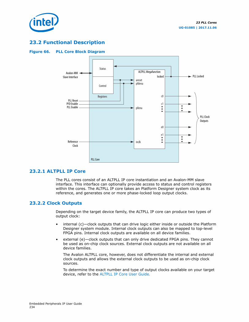
23.2 Functional Description
Figure 66. PLL Core Block Diagram
Status
Control
aresetpfdena
pllena
inclk
e1
e0
c1
c0Registers
ALTPLL MegafunctionPLL Lockedlocked
PLL ClockOutputs
ReferenceClock
PLL ResetPFD EnablePLL Enable
Avalon-MMSlave Interface
PLL Core
23.2.1 ALTPLL IP Core
The PLL cores consist of an ALTPLL IP core instantiation and an Avalon-MM slaveinterface. This interface can optionally provide access to status and control registerswithin the cores. The ALTPLL IP core takes an Platform Designer system clock as itsreference, and generates one or more phase-locked loop output clocks.
23.2.2 Clock Outputs
Depending on the target device family, the ALTPLL IP core can produce two types ofoutput clock:
• internal (c)—clock outputs that can drive logic either inside or outside the PlatformDesigner system module. Internal clock outputs can also be mapped to top-levelFPGA pins. Internal clock outputs are available on all device families.
• external (e)—clock outputs that can only drive dedicated FPGA pins. They cannotbe used as on-chip clock sources. External clock outputs are not available on alldevice families.
The Avalon ALTPLL core, however, does not differentiate the internal and externalclock outputs and allows the external clock outputs to be used as on-chip clocksources.
To determine the exact number and type of output clocks available on your targetdevice, refer to the ALTPLL IP Core User Guide.
23 PLL Cores
UG-01085 | 2017.11.06
Embedded Peripherals IP User Guide234

23.2.3 PLL Status and Control Signals
Depending on how the ALTPLL IP core is parameterized, there can be a variablenumber of status and control signals. You can choose to export certain status andcontrol signals to the top-level Platform Designer system module. Alternatively,Avalon-MM registers can provide access to the signals. Any status or control signalswhich are not mapped to registers are exported to the top-level module. For details,refer to the Instantiating the Avalon ALTPLL Core.
23.2.4 System Reset Considerations
At FPGA configuration, the PLL cores reset automatically. PLL-specific reset circuitryguarantees that the PLL locks before releasing reset for the overall Platform Designersystem module.
Resetting the PLL resets the entire Platform Designer system module.
23.3 Instantiating the Avalon ALTPLL Core
When you instantiate the Avalon ALTPLL core, the MegaWizard Plug-In Manager isautomatically launched for you to parameterize the ALTPLL IP core. There are noadditional parameters that you can configure in Platform Designer.
The pfdena signal of the ALTPLL IP core is not exported to the top level of thePlatform Designer module. You can drive this port by writing to the PFDENA bit in thecontrol register.
The locked, pllena/extclkena, and areset signals of the IP core are alwaysexported to the top level of the Platform Designer module. You can read the lockedsignal and reset the core by manipulating respective bits in the registers. See theRegister Definitions and Bit List section for more information on the registers.
For details about using the ALTPLL MegaWizard Plug-In Manager, refer to the ALTPLLIP Core User Guide.
23.4 Instantiating the PLL Core
This section describes the options available in the MegaWizard™ interface for the PLLcore in Platform Designer.
PLL Settings Page
The PLL Settings page contains a button that launches the ALTPLL MegaWizard Plug-In Manager. Use the MegaWizard Plug-In Manager to parameterize the ALTPLL IP core.The set of available parameters depends on the target device family.
You cannot click Finish in the PLL wizard nor configure the PLL interface until youparameterize the ALTPLL IP core.
Interface Page
The Interface page configures the access modes for the optional advanced PLL statusand control signals.
23 PLL Cores
UG-01085 | 2017.11.06
Embedded Peripherals IP User Guide235

For each advanced signal present on the ALTPLL IP core, you can select one of thefollowing access modes:
• Export—Exports the signal to the top level of the Platform Designer systemmodule.
• Register—Maps the signal to a bit in a status or control register.
The advanced signals are optional. If you choose not to create any of them in theALTPLL MegaWizard Plug-In, the PLL's default behavior is as shown in below.
You can specify the access mode for the advanced signals shown in below. TheALTPLL core signals, not displayed in this table, are automatically exported to thetop level of the Platform Designer system module.
Table 182. ALTPLL Advanced Signal
ALTPLLName
Input /Output
Avalon-MM PLL WizardName
Default Behavior Description
areset input PLL Reset Input The PLL is reset only atdevice configuration.
This signal resets the entire PlatformDesigner system module, and restores thePLL to its initial settings.
pllena input PLL Enable Input The PLL is enabled. This signal enables the PLL.pllena is always exported.
pfdena input PFD Enable Input The phase-frequencydetector is enabled.
This signal enables the phase-frequencydetector in the PLL, allowing it to lock on tochanges in the clock reference.
locked output PLL Locked Output — This signal is asserted when the PLL islocked to the input clock.
Asserting areset resets the entire Platform Designer system module, not just thePLL.
Finish
Click Finish to insert the PLL into the Platform Designer system. The PLL clockoutput(s) appear in the clock settings table on the Platform Designer SystemContents tab.
If the PLL has external output clocks, they appear in the clock settings table like otherclocks; however, you cannot use them to drive components within the PlatformDesigner system.
For details about using external output clocks, refer to the ALTPLL IP Core User Guide.
The Platform Designer automatically connects the PLL's reference clock input to thefirst available clock in the clock settings table.
If there is more than one Platform Designer system clock available, verify that the PLLis connected to the appropriate reference clock.
23.5 Hardware Simulation Considerations
The HDL files generated by Platform Designer for the PLL cores are suitable for bothsynthesis and simulation. The PLL cores support the standard Platform Designersimulation flow, so there are no special considerations for hardware simulation.
23 PLL Cores
UG-01085 | 2017.11.06
Embedded Peripherals IP User Guide236
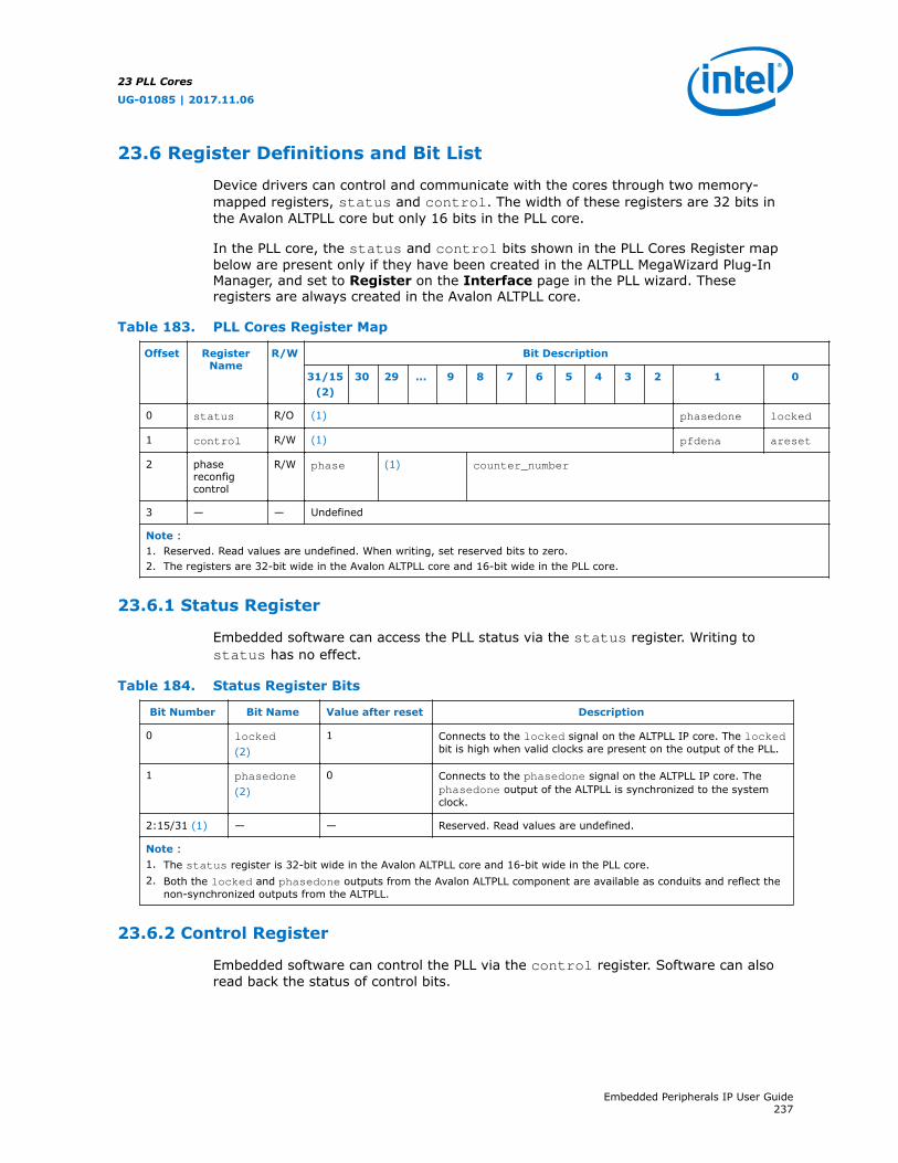
23.6 Register Definitions and Bit List
Device drivers can control and communicate with the cores through two memory-mapped registers, status and control. The width of these registers are 32 bits inthe Avalon ALTPLL core but only 16 bits in the PLL core.
In the PLL core, the status and control bits shown in the PLL Cores Register mapbelow are present only if they have been created in the ALTPLL MegaWizard Plug-InManager, and set to Register on the Interface page in the PLL wizard. Theseregisters are always created in the Avalon ALTPLL core.
Table 183. PLL Cores Register Map
Offset RegisterName
R/W Bit Description
31/15(2)
30 29 ... 9 8 7 6 5 4 3 2 1 0
0 status R/O (1) phasedone locked
1 control R/W (1) pfdena areset
2 phasereconfigcontrol
R/W phase (1) counter_number
3 — — Undefined
Note :1. Reserved. Read values are undefined. When writing, set reserved bits to zero.2. The registers are 32-bit wide in the Avalon ALTPLL core and 16-bit wide in the PLL core.
23.6.1 Status Register
Embedded software can access the PLL status via the status register. Writing tostatus has no effect.
Table 184. Status Register Bits
Bit Number Bit Name Value after reset Description
0 locked
(2)1 Connects to the locked signal on the ALTPLL IP core. The locked
bit is high when valid clocks are present on the output of the PLL.
1 phasedone
(2)0 Connects to the phasedone signal on the ALTPLL IP core. The
phasedone output of the ALTPLL is synchronized to the systemclock.
2:15/31 (1) — — Reserved. Read values are undefined.
Note :1. The status register is 32-bit wide in the Avalon ALTPLL core and 16-bit wide in the PLL core.2. Both the locked and phasedone outputs from the Avalon ALTPLL component are available as conduits and reflect the
non-synchronized outputs from the ALTPLL.
23.6.2 Control Register
Embedded software can control the PLL via the control register. Software can alsoread back the status of control bits.
23 PLL Cores
UG-01085 | 2017.11.06
Embedded Peripherals IP User Guide237

Table 185. Control Register Bits
Bit Number Bit Name Value after reset Description
0 areset 0 Connects to the areset signal on the ALTPLL IP core. Writing a 1to this bit initiates a PLL reset.
1 pfdena 1 Connects to the pfdena signal on the ALTPLL IP core. Writing a 0to this bit disables the phase frequency detection.
2:15/31 (1) — — Reserved. Read values are undefined. When writing, set reservedbits to zero.
Note :1. The controlregister is 32-bit wide in the Avalon ALTPLL core and 16-bit wide in the PLL core.
23.6.3 Phase Reconfig Control Register
Embedded software can control the dynamic phase reconfiguration via the phasereconfig control register.
Table 186. Phase Reconfig Control Register Bits
Bit Number Bit Name Value afterreset
Description
0:8 counter_number — A binary 9-bit representation of the counter that needs to bereconfigured. Refer to the Counter_Number Bits and Selectiontable for the counter selection.
9:29 — — Reserved. Read values are undefined. When writing, set reservedbits to zero.
30:31 phase (1) — 01: Step up phase of counter_number10: Step down phase of counter_number00 and 11: No operation
Note :1. Phase step up or down when set to 1 (only applicable to the Avalon ALTPLL core).
The table below lists the counter number and selection. For example, 100 000 000selects counter C0 and 100 000 001 selects counter C1.
Table 187. Counter_Number Bits and Selection
Counter_Number [0:8] Counter Selection
0 0000 0000 All output counters
0 0000 0001 M counter
> 0 0000 0001 Undefined
1 0000 0000 C0
1 0000 0001 C1
1 0000 0010 C2
... ...
1 0000 1000 C8
1 0000 1001 C9
> 1 0000 1001 Undefined
23 PLL Cores
UG-01085 | 2017.11.06
Embedded Peripherals IP User Guide238
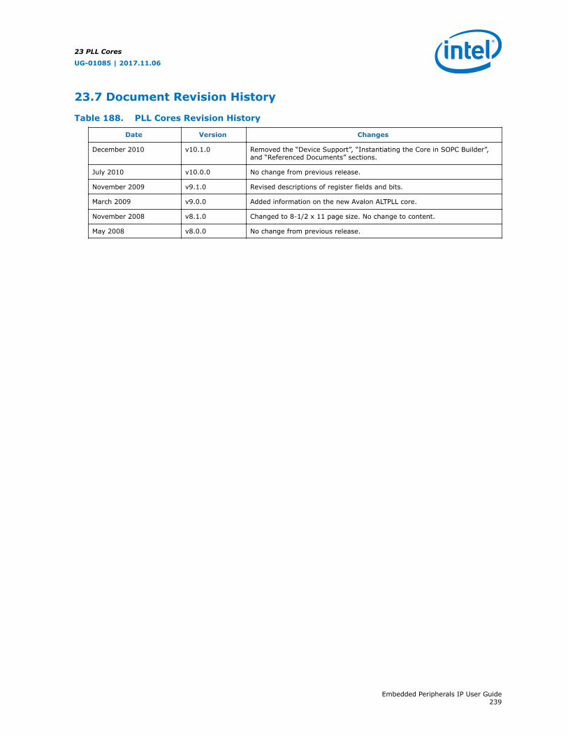
23.7 Document Revision History
Table 188. PLL Cores Revision History
Date Version Changes
December 2010 v10.1.0 Removed the “Device Support”, “Instantiating the Core in SOPC Builder”,and “Referenced Documents” sections.
July 2010 v10.0.0 No change from previous release.
November 2009 v9.1.0 Revised descriptions of register fields and bits.
March 2009 v9.0.0 Added information on the new Avalon ALTPLL core.
November 2008 v8.1.0 Changed to 8-1/2 x 11 page size. No change to content.
May 2008 v8.0.0 No change from previous release.
23 PLL Cores
UG-01085 | 2017.11.06
Embedded Peripherals IP User Guide239
24 DMA Controller Core
24.1 Core Overview
The direct memory access (DMA) controller core with Avalon interface performs bulkdata transfers, reading data from a source address range and writing the data to adifferent address range. An Avalon Memory-Mapped (Avalon-MM) master peripheral,such as a CPU, can offload memory transfer tasks to the DMA controller. While theDMA controller performs memory transfers, the master is free to perform other tasksin parallel.
The DMA controller transfers data as efficiently as possible, reading and writing dataat the maximum pace allowed by the source or destination. The DMA controller iscapable of performing Avalon transfers with flow control, enabling it to automaticallytransfer data to or from a slow peripheral with flow control (for example, UART), atthe maximum pace allowed by the peripheral.
Instantiating the DMA controller in Platform Designer creates one slave port and twomaster ports. You must specify which slave peripherals can be accessed by the readand write master ports. Likewise, you must specify which other master peripheral(s)can access the DMA control port and initiate DMA transactions. The DMA controllerdoes not export any signals to the top level of the system module.
Note: While instantiating the DMA controller in the hierarchical subsystem, add an Avalon-MM pipeline bridge in front of the exported master interface of the DMA controller inthe subsystem. This will allow you to configure the bus width of the pipeline bridge tomatch the slave address bus.
For the Nios II processor, device drivers are provided in the HAL system library. Seethe Software Programming Model section for details of HAL support.
24.2 Functional Description
You can use the DMA controller to perform data transfers from a source address-spaceto a destination address-space. The controller has no concept of endianness and doesnot interpret the payload data. The concept of endianness only applies to a masterthat interprets payload data.
The source and destination may be either an Avalon-MM slave peripheral (for example,a constant address) or an address range in memory. The DMA controller can be usedin conjunction with peripherals with flow control, which allows data transactions offixed or variable length. The DMA controller can signal an interrupt request (IRQ)when a DMA transaction completes. A transaction is a sequence of one or more Avalontransfers initiated by the DMA controller core.
UG-01085 | 2017.11.06
Intel Corporation. All rights reserved. Intel, the Intel logo, Altera, Arria, Cyclone, Enpirion, MAX, Nios, Quartusand Stratix words and logos are trademarks of Intel Corporation or its subsidiaries in the U.S. and/or othercountries. Intel warrants performance of its FPGA and semiconductor products to current specifications inaccordance with Intel's standard warranty, but reserves the right to make changes to any products and servicesat any time without notice. Intel assumes no responsibility or liability arising out of the application or use of anyinformation, product, or service described herein except as expressly agreed to in writing by Intel. Intelcustomers are advised to obtain the latest version of device specifications before relying on any publishedinformation and before placing orders for products or services.*Other names and brands may be claimed as the property of others.
ISO9001:2008Registered

The DMA controller has two Avalon-MM master ports—a master read port and amaster write port—and one Avalon-MM slave port for controlling the DMA as shown inthe figure below.
Figure 67. DMA Controller Block Diagram
Addr,data,
control
IRQ
Register File
status
readaddress
length
control
Avalon-MMSlave Port
SeparateAvalon-MMMaster Ports
ReadMaster
Port
WriteMaster
Port
writeaddressControl
Port
A typical DMA transaction proceeds as follows:
1. A CPU prepares the DMA controller for a transaction by writing to the control port.
2. The CPU enables the DMA controller. The DMA controller then begins transferringdata without additional intervention from the CPU. The DMA’s master read portreads data from the read address, which may be a memory or a peripheral. Themaster write port writes the data to the destination address, which can also be amemory or peripheral. A shallow FIFO buffers data between the read and writeports.
3. The DMA transaction ends when a specified number of bytes are transferred (afixed-length transaction) or an end-of-packet signal is asserted by either thesender or receiver (a variable-length transaction). At the end of the transaction,the DMA controller generates an interrupt request (IRQ) if it was configured by theCPU to do so.
4. During or after the transaction, the CPU can determine if a transaction is inprogress, or if the transaction ended (and how) by examining the DMA controller’sstatus register.
24.2.1 Setting Up DMA Transactions
An Avalon-MM master peripheral sets up and initiates DMA transactions by writing toregisters via the control port. The Avalon-MM master programs the DMA engine usingbyte addresses which are byte aligned. The master peripheral configures the followingoptions:
24 DMA Controller Core
UG-01085 | 2017.11.06
Embedded Peripherals IP User Guide241

• Read (source) address location
• Write (destination) address location
• Size of the individual transfers: Byte (8-bit), halfword (16-bit), word (32-bit),doubleword (64-bit) or quadword (128-bit)
• Enable interrupt upon end of transaction
• Enable source or destination to end the DMA transaction with end-of-packet signal
• Specify whether source and destination are memory or peripheral
The master peripheral then sets a bit in the control register to initiate the DMAtransaction.
24.2.2 The Master Read and Write Ports
The DMA controller reads data from the source address through the master read port,and then writes to the destination address through the master write port. You programthe DMA controller using byte addresses. Read and write start addresses should bealigned to the transfer size. For example, to transfer data words, if the start address is0, the address will increment to 4, 8, and 12. For heterogeneous systems where anumber of different slave devices are of different widths, the data width for read andwrite masters matches the width of the widest data-width slave addressed by eitherthe read or the write master. For bursting transfers, the burst length is set to the DMAtransaction length with the appropriate unit conversion. For example, if a 32-bit datawidth DMA is programmed for a word transfer of 64 bytes, the length registered isprogrammed with 64 and the burst count port will be 16. If a 64-bit data width DMA isprogrammed for a doubleword transfer of 8 bytes, the length register is programmedwith 8 and the burst count port will be 1.
There is a shallow FIFO buffer between the master read and write ports. The defaultdepth is 2, which makes the write action depend on the data-available status of theFIFO, rather than on the status of the master read port.
Both the read and write master ports can perform Avalon transfers with flow control,which allows the slave peripheral to control the flow of data and terminate the DMAtransaction.
For details about flow control in Avalon-MM data transfers and Avalon-MM peripherals,refer to Avalon Interface Specifications.
24.2.3 Addressing and Address Incrementing
When accessing memory, the read (or write) address increments by 1, 2, 4, 8, or 16after each access, depending on the width of the data. On the other hand, a typicalperipheral device (such as UART) has fixed register locations. In this case, the read/write address is held constant throughout the DMA transaction.
24 DMA Controller Core
UG-01085 | 2017.11.06
Embedded Peripherals IP User Guide242

The rules for address incrementing are, in order of priority:
• If the control register’s RCON (or WCON) bit is set, the read (or write) incrementvalue is 0.
• Otherwise, the read and write increment values are set according to the transfersize specified in the control register, as shown below.
Table 189. Address Increment Values
Transfer Width Increment
byte 1
halfword 2
word 4
doubleword 8
quadword 16
In systems with heterogeneous data widths, care must be taken to present thecorrect address or offset when configuring the DMA to access native-alignedslaves. For example, in a system using a 32-bit Nios II processor and a 16-bitDMA, the base address for the UART txdata register must be divided by thedma_data_width/cpu_data_width—2 in this example.
24.3 Parameters
This section describes the parameters you can configure.
24.3.1 DMA Parameters (Basic)
The DMA Parameters page includes the following parameters.
Transfer Size
The parameter Width of the DMA Length Register specifies the minimum width ofthe DMA’s transaction length register, which can be between 1 and 32. The lengthregister determines the maximum number of transfers possible in a single DMAtransaction.
By default, the length register is wide enough to span any of the slave peripheralsmastered by the read or write ports. Overriding the length register may be necessaryif the DMA master port (read or write) masters only data peripherals, such as a UART.In this case, the address span of each slave is small, but a larger number of transfersmay be desired per DMA transaction.
Burst Transactions
When Enable Burst Transfers is turned on, the DMA controller performs bursttransactions on its master read and write ports. The parameter Maximum Burst Sizedetermines the maximum burst size allowed in a transaction.
In burst mode, the length of a transaction must not be longer than the configuredmaximum burst size. Otherwise, the transaction must be performed as multipletransactions.
24 DMA Controller Core
UG-01085 | 2017.11.06
Embedded Peripherals IP User Guide243
FIFO Depth
The parameter Data Transfer FIFO Depth specifies the depth of the FIFO bufferused for data transfers. Intel recommends that you set the depth of the FIFO buffer toat least twice the maximum read latency of the slave interface connected to the readmaster port. A depth that is too low reduces transfer throughput.
FIFO Implementation
This option determines the implementation of the FIFO buffer between the masterread and write ports. Select Construct FIFO from Registers to implement the FIFOusing one register per storage bit. This option has a strong impact on logic utilizationwhen the DMA controller’s data width is large. See the Advanced Options section.
To implement the FIFO using embedded memory blocks available in the FPGA, selectConstruct FIFO from Memory Blocks.
24.3.2 Advanced Options
The Advanced Options page includes the following parameters.
Allowed Transactions
You can choose the transfer datawidth(s) supported by the DMA controller hardware.The following datawidth options can be enabled or disabled:
• Byte
• Halfword (two bytes)
• Word (four bytes)
• Doubleword (eight bytes)
• Quadword (sixteen bytes)
Disabling unnecessary transfer widths reduces the number of on-chip logicresources consumed by the DMA controller core. For example, if a system hasboth 16-bit and 32-bit memories, but the DMA controller transfers data to the 16-bit memory, 32-bit transfers could be disabled to conserve logic resources.
24.4 Software Programming Model
This section describes the programming model for the DMA controller, including theregister map and software declarations to access the hardware. For Nios II processorusers, Intel provides HAL system library drivers that enable you to access the DMAcontroller core using the HAL API for DMA devices.
24.4.1 HAL System Library Support
The Intel-provided driver implements a HAL DMA device driver that integrates into theHAL system library for Nios II systems. HAL users should access the DMA controllervia the familiar HAL API, rather than accessing the registers directly.
If your program uses the HAL device driver to access the DMA controller, accessing thedevice registers directly interferes with the correct behavior of the driver.
24 DMA Controller Core
UG-01085 | 2017.11.06
Embedded Peripherals IP User Guide244
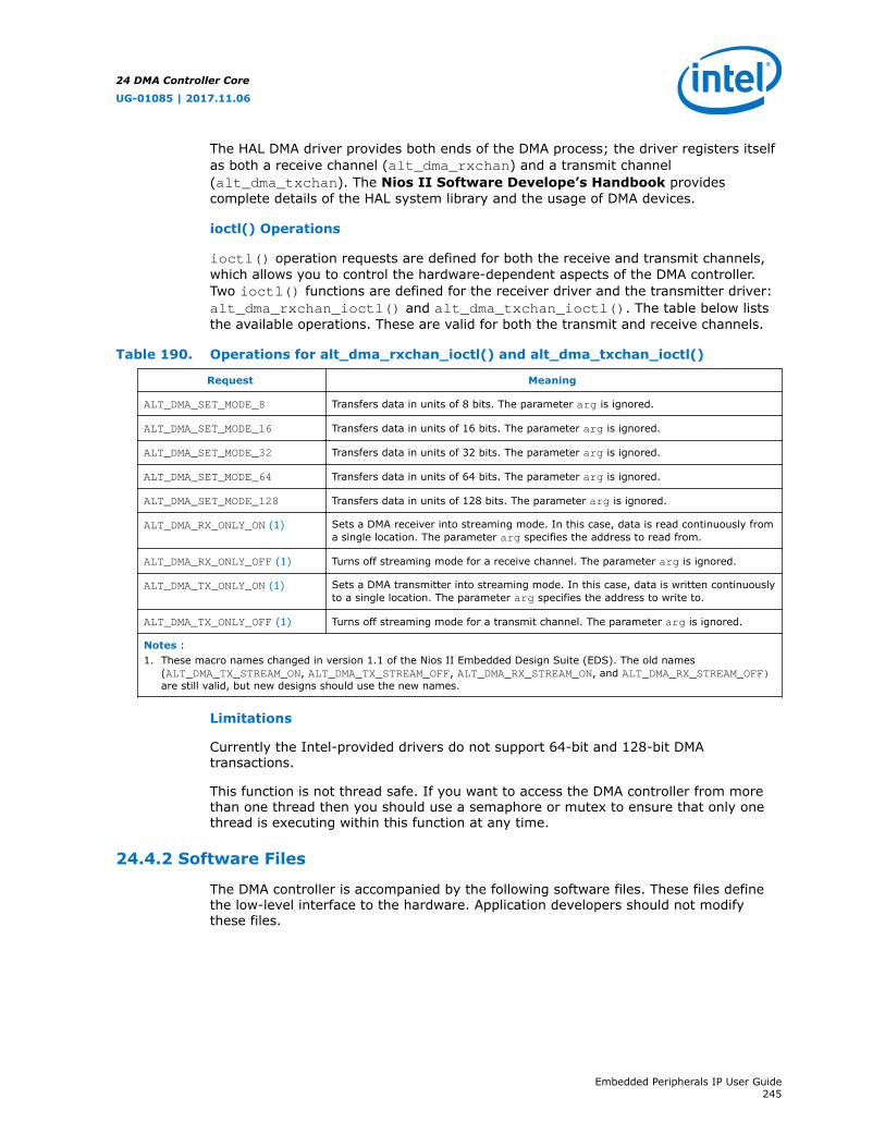
The HAL DMA driver provides both ends of the DMA process; the driver registers itselfas both a receive channel (alt_dma_rxchan) and a transmit channel(alt_dma_txchan). The Nios II Software Develope’s Handbook providescomplete details of the HAL system library and the usage of DMA devices.
ioctl() Operations
ioctl() operation requests are defined for both the receive and transmit channels,which allows you to control the hardware-dependent aspects of the DMA controller.Two ioctl() functions are defined for the receiver driver and the transmitter driver:alt_dma_rxchan_ioctl() and alt_dma_txchan_ioctl(). The table below liststhe available operations. These are valid for both the transmit and receive channels.
Table 190. Operations for alt_dma_rxchan_ioctl() and alt_dma_txchan_ioctl()
Request Meaning
ALT_DMA_SET_MODE_8 Transfers data in units of 8 bits. The parameter arg is ignored.
ALT_DMA_SET_MODE_16 Transfers data in units of 16 bits. The parameter arg is ignored.
ALT_DMA_SET_MODE_32 Transfers data in units of 32 bits. The parameter arg is ignored.
ALT_DMA_SET_MODE_64 Transfers data in units of 64 bits. The parameter arg is ignored.
ALT_DMA_SET_MODE_128 Transfers data in units of 128 bits. The parameter arg is ignored.
ALT_DMA_RX_ONLY_ON (1) Sets a DMA receiver into streaming mode. In this case, data is read continuously froma single location. The parameter arg specifies the address to read from.
ALT_DMA_RX_ONLY_OFF (1) Turns off streaming mode for a receive channel. The parameter arg is ignored.
ALT_DMA_TX_ONLY_ON (1) Sets a DMA transmitter into streaming mode. In this case, data is written continuouslyto a single location. The parameter arg specifies the address to write to.
ALT_DMA_TX_ONLY_OFF (1) Turns off streaming mode for a transmit channel. The parameter arg is ignored.
Notes :1. These macro names changed in version 1.1 of the Nios II Embedded Design Suite (EDS). The old names
(ALT_DMA_TX_STREAM_ON, ALT_DMA_TX_STREAM_OFF, ALT_DMA_RX_STREAM_ON, and ALT_DMA_RX_STREAM_OFF)are still valid, but new designs should use the new names.
Limitations
Currently the Intel-provided drivers do not support 64-bit and 128-bit DMAtransactions.
This function is not thread safe. If you want to access the DMA controller from morethan one thread then you should use a semaphore or mutex to ensure that only onethread is executing within this function at any time.
24.4.2 Software Files
The DMA controller is accompanied by the following software files. These files definethe low-level interface to the hardware. Application developers should not modifythese files.
24 DMA Controller Core
UG-01085 | 2017.11.06
Embedded Peripherals IP User Guide245
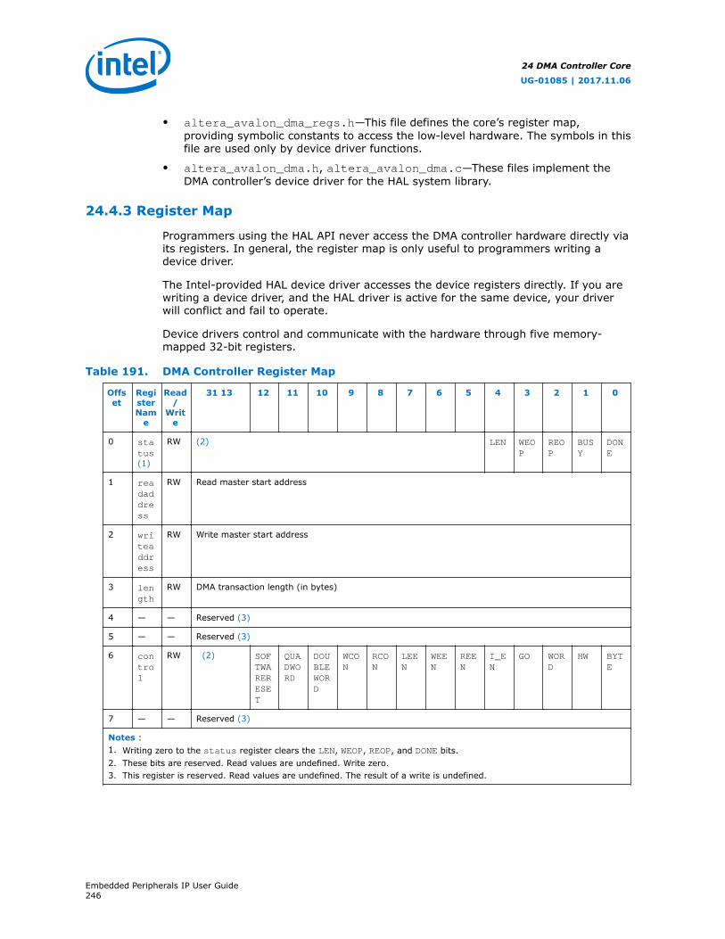
• altera_avalon_dma_regs.h—This file defines the core’s register map,providing symbolic constants to access the low-level hardware. The symbols in thisfile are used only by device driver functions.
• altera_avalon_dma.h, altera_avalon_dma.c—These files implement theDMA controller’s device driver for the HAL system library.
24.4.3 Register Map
Programmers using the HAL API never access the DMA controller hardware directly viaits registers. In general, the register map is only useful to programmers writing adevice driver.
The Intel-provided HAL device driver accesses the device registers directly. If you arewriting a device driver, and the HAL driver is active for the same device, your driverwill conflict and fail to operate.
Device drivers control and communicate with the hardware through five memory-mapped 32-bit registers.
Table 191. DMA Controller Register Map
Offset
RegisterNam
e
Read/
Write
31 13 12 11 10 9 8 7 6 5 4 3 2 1 0
0 status (1)
RW (2) LEN WEOP
REOP
BUSY
DONE
1 readaddress
RW Read master start address
2 writeaddress
RW Write master start address
3 length
RW DMA transaction length (in bytes)
4 — — Reserved (3)
5 — — Reserved (3)
6 control
RW (2) SOFTWARERESET
QUADWORD
DOUBLEWORD
WCON
RCON
LEEN
WEEN
REEN
I_EN
GO WORD
HW BYTE
7 — — Reserved (3)
Notes :1. Writing zero to the status register clears the LEN, WEOP, REOP, and DONE bits.2. These bits are reserved. Read values are undefined. Write zero.3. This register is reserved. Read values are undefined. The result of a write is undefined.
24 DMA Controller Core
UG-01085 | 2017.11.06
Embedded Peripherals IP User Guide246
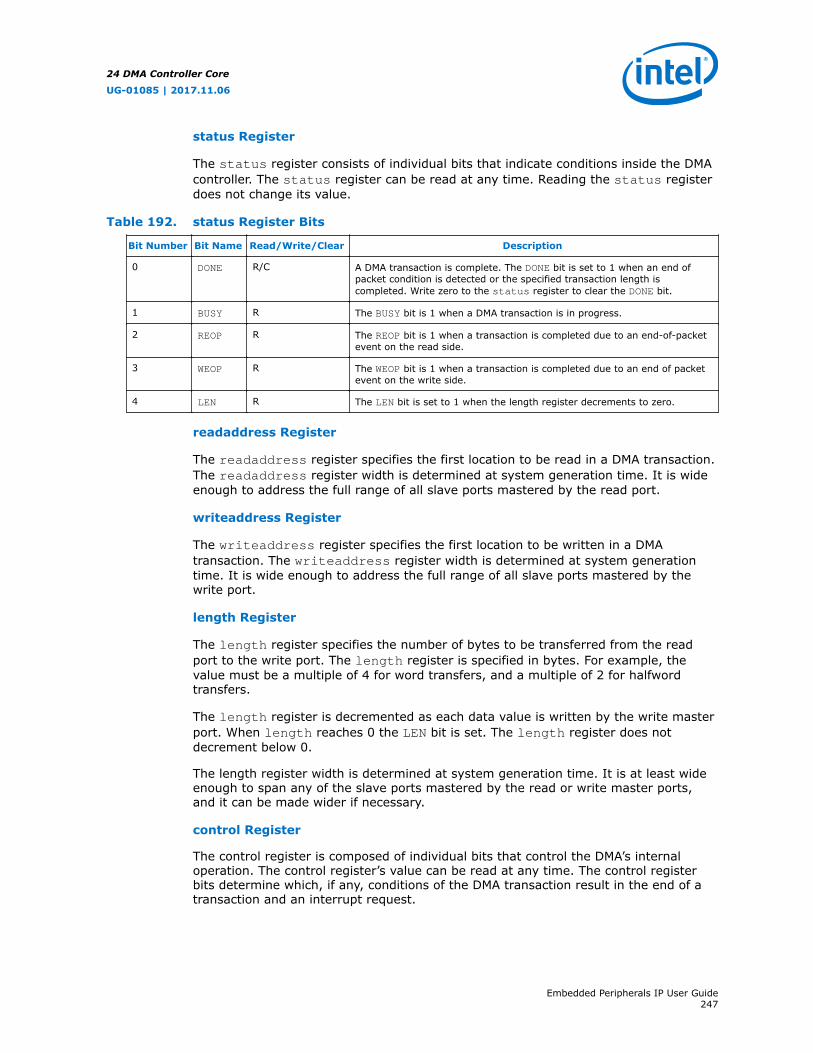
status Register
The status register consists of individual bits that indicate conditions inside the DMAcontroller. The status register can be read at any time. Reading the status registerdoes not change its value.
Table 192. status Register Bits
Bit Number Bit Name Read/Write/Clear Description
0 DONE R/C A DMA transaction is complete. The DONE bit is set to 1 when an end ofpacket condition is detected or the specified transaction length iscompleted. Write zero to the status register to clear the DONE bit.
1 BUSY R The BUSY bit is 1 when a DMA transaction is in progress.
2 REOP R The REOP bit is 1 when a transaction is completed due to an end-of-packetevent on the read side.
3 WEOP R The WEOP bit is 1 when a transaction is completed due to an end of packetevent on the write side.
4 LEN R The LEN bit is set to 1 when the length register decrements to zero.
readaddress Register
The readaddress register specifies the first location to be read in a DMA transaction.The readaddress register width is determined at system generation time. It is wideenough to address the full range of all slave ports mastered by the read port.
writeaddress Register
The writeaddress register specifies the first location to be written in a DMAtransaction. The writeaddress register width is determined at system generationtime. It is wide enough to address the full range of all slave ports mastered by thewrite port.
length Register
The length register specifies the number of bytes to be transferred from the readport to the write port. The length register is specified in bytes. For example, thevalue must be a multiple of 4 for word transfers, and a multiple of 2 for halfwordtransfers.
The length register is decremented as each data value is written by the write masterport. When length reaches 0 the LEN bit is set. The length register does notdecrement below 0.
The length register width is determined at system generation time. It is at least wideenough to span any of the slave ports mastered by the read or write master ports,and it can be made wider if necessary.
control Register
The control register is composed of individual bits that control the DMA’s internaloperation. The control register’s value can be read at any time. The control registerbits determine which, if any, conditions of the DMA transaction result in the end of atransaction and an interrupt request.
24 DMA Controller Core
UG-01085 | 2017.11.06
Embedded Peripherals IP User Guide247

Table 193. Control Register Bits
BitNumber
Bit Name Read/Write/Clear
Description
0 BYTE RW Specifies byte transfers.
1 HW RW Specifies halfword (16-bit) transfers.
2 WORD RW Specifies word (32-bit) transfers.
3 GO RW Enables DMA transaction. When the GO bit is set to 0 during idle stage(before execution starts), the DMA is prevented from executingtransfers. When the GO bit is set to 1 during idle stage and the lengthregister is non-zero, transfers occur.If go bit is de-asserted low before write transaction complete, done bitwill never go high. It is advisable that GO bit is modified during idlestage (no execution happened) only.
4 I_EN RW Enables interrupt requests (IRQ). When the I_EN bit is 1, the DMAcontroller generates an IRQ when the status register’s DONE bit is set to1. IRQs are disabled when the I_EN bit is 0.
5 REEN RW Ends transaction on read-side end-of-packet. When the REEN bit is setto 1, a slave port with flow control on the read side may end the DMAtransaction by asserting its end-of-packet signal. REEN bit should be setto 0.
6 WEEN RW Ends transaction on write-side end-of-packet. WEEN bit should be setto 0.
7 LEEN RW Ends transaction when the length register reaches zero. When this bitis 0, length reaching 0 does not cause a transaction to end. In thiscase, the DMA transaction must be terminated by an end-of-packetsignal from either the read or write master port. LEEN bit should be setto 1.
8 RCON RW Reads from a constant address. When RCON is 0, the read addressincrements after every data transfer. This is the mechanism for the DMAcontroller to read a range of memory addresses. When RCON is 1, theread address does not increment. This is the mechanism for the DMAcontroller to read from a peripheral at a constant memory address. Fordetails, see the Addressing and Address Incrementing section.
9 WCON RW Writes to a constant address. Similar to the RCON bit, when WCON is 0the write address increments after every data transfer; when WCON is 1the write address does not increment. For details, see Addressing andAddress Incrementing.
10 DOUBLEWORD RW Specifies doubleword transfers.
11 QUADWORD RW Specifies quadword transfers.
12 SOFTWARERESET RW Software can reset the DMA engine by writing this bit to 1 twice. Uponthe second write of 1 to the SOFTWARERESET bit, the DMA control isreset identically to a system reset. The logic which sequences thesoftware reset process then resets itself automatically.
The data width of DMA transactions is specified by the BYTE, HW, WORD, DOUBLEWORD,and QUADWORD bits. Only one of these bits can be set at a time. If more than one ofthe bits is set, the DMA controller behavior is undefined. The width of the transfer isdetermined by the narrower of the two slaves read and written. For example, a DMAtransaction that reads from a 16-bit flash memory and writes to a 32-bit on-chipmemory requires a halfword transfer. In this case, HW must be set to 1, and BYTE,WORD, DOUBLEWORD, and QUADWORD must be set to 0.
24 DMA Controller Core
UG-01085 | 2017.11.06
Embedded Peripherals IP User Guide248
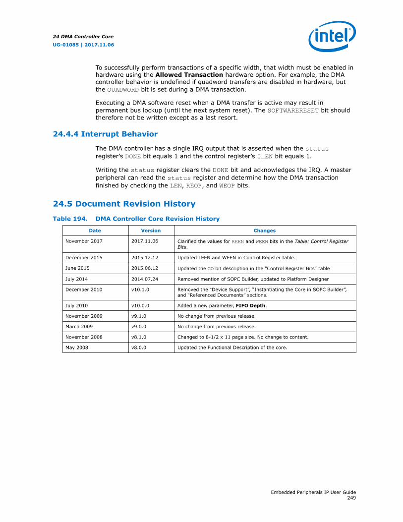
To successfully perform transactions of a specific width, that width must be enabled inhardware using the Allowed Transaction hardware option. For example, the DMAcontroller behavior is undefined if quadword transfers are disabled in hardware, butthe QUADWORD bit is set during a DMA transaction.
Executing a DMA software reset when a DMA transfer is active may result inpermanent bus lockup (until the next system reset). The SOFTWARERESET bit shouldtherefore not be written except as a last resort.
24.4.4 Interrupt Behavior
The DMA controller has a single IRQ output that is asserted when the statusregister’s DONE bit equals 1 and the control register’s I_EN bit equals 1.
Writing the status register clears the DONE bit and acknowledges the IRQ. A masterperipheral can read the status register and determine how the DMA transactionfinished by checking the LEN, REOP, and WEOP bits.
24.5 Document Revision History
Table 194. DMA Controller Core Revision History
Date Version Changes
November 2017 2017.11.06 Clarified the values for REEN and WEEN bits in the Table: Control RegisterBits.
December 2015 2015.12.12 Updated LEEN and WEEN in Control Register table.
June 2015 2015.06.12 Updated the GO bit description in the "Control Register Bits" table
July 2014 2014.07.24 Removed mention of SOPC Builder, updated to Platform Designer
December 2010 v10.1.0 Removed the “Device Support”, “Instantiating the Core in SOPC Builder”,and “Referenced Documents” sections.
July 2010 v10.0.0 Added a new parameter, FIFO Depth.
November 2009 v9.1.0 No change from previous release.
March 2009 v9.0.0 No change from previous release.
November 2008 v8.1.0 Changed to 8-1/2 x 11 page size. No change to content.
May 2008 v8.0.0 Updated the Functional Description of the core.
24 DMA Controller Core
UG-01085 | 2017.11.06
Embedded Peripherals IP User Guide249
25 Modular Scatter-Gather DMA Core
25.1 Core Overview
In a processor subsystem, data transfers between two memory spaces can happenfrequently. In order to offload the processor from moving data around a system, aDirect Memory Access (DMA) engine is introduced to perform this function instead.The Modular Scatter-Gather DMA (mSGDMA) is capable of performing data movementoperations with preloaded instructions, called descriptors. Multiple descriptors withdifferent transfer sizes, and source and destination addresses have the option totrigger interrupts.
The mSGDMA core has a modular design that facilitates easy integration with theFPGA fabric. The core consists of a dispatcher block with optional read master andwrite master blocks. The descriptor block receives and decodes the descriptor, anddispatches instructions to the read master and write master blocks for furtheroperation. The block is also configured to transfer additional information to the host.In this context, the read master block reads data through its Avalon-MM masterinterface, and channels it into the Avalon-ST source interface, based on instructiongiven by the dispatcher block. Conversely, the write master block receives data fromits Avalon-ST sink interface and writes it to the destination address via its Avalon-MMmaster interface.
25.2 Feature Description
The mSGDMA provides three configuration structures for handling data transfersbetween the Avalon-MM to Avalon-MM, Avalon-MM to Avalon-ST, and Avalon-ST toAvalon-MM modes. The sub-core of the mSGDMA is instantiated automaticallyaccording to the structure configured for the mSGDMA use model.
UG-01085 | 2017.11.06
Intel Corporation. All rights reserved. Intel, the Intel logo, Altera, Arria, Cyclone, Enpirion, MAX, Nios, Quartusand Stratix words and logos are trademarks of Intel Corporation or its subsidiaries in the U.S. and/or othercountries. Intel warrants performance of its FPGA and semiconductor products to current specifications inaccordance with Intel's standard warranty, but reserves the right to make changes to any products and servicesat any time without notice. Intel assumes no responsibility or liability arising out of the application or use of anyinformation, product, or service described herein except as expressly agreed to in writing by Intel. Intelcustomers are advised to obtain the latest version of device specifications before relying on any publishedinformation and before placing orders for products or services.*Other names and brands may be claimed as the property of others.
ISO9001:2008Registered

Figure 68. mSGDMA Module Configuration with support for Memory-Mapped Reads andWrites
Figure 69. mSGDMA Module Configuration with Support for Memory-Mapped StreamingReads to the Avalon-ST data bus
25 Modular Scatter-Gather DMA Core
UG-01085 | 2017.11.06
Embedded Peripherals IP User Guide251

Figure 70. mSGDMA Module Configuration with Support for Avalon-ST Data WriteStreaming to the Memory-Mapped Bus
The mSGDMA support 32-bit addressing by default. However, the core can support 64-bit addressing when you select Extended Feature Options in the parameter editor.It also supports extended features such as dynamic burst count programming, strideaddressing, extended discriptor format (64-bit addressing), and unique sequencenumber identification for executed descriptor.
25.3 mSGDMA Interfaces and Parameters
25.3.1 Interface
The mSGDMA consists of the following:
• One Avalon-MM CSR slave port.
• One configurable Avalon-MM Slave or Avalon-ST Source Response port.
• Source and destination data path ports, which can be Avalon-MM or Avalon-ST.
The mSGDMA also provides an active-high-level interrupt output.
Only one clock domain can drive the mSGDMA. The requirement of different clockdomains between source and destination data paths are handled by the PlatformDesigner fabric.
A hardware reset resets the whole system. Software reset resets the registers andFIFOs of the dispatchers of the dispatcher and master modules. For a software reset,read the resetting bit of the status register to determine when a full reset cyclecompletes.
25 Modular Scatter-Gather DMA Core
UG-01085 | 2017.11.06
Embedded Peripherals IP User Guide252
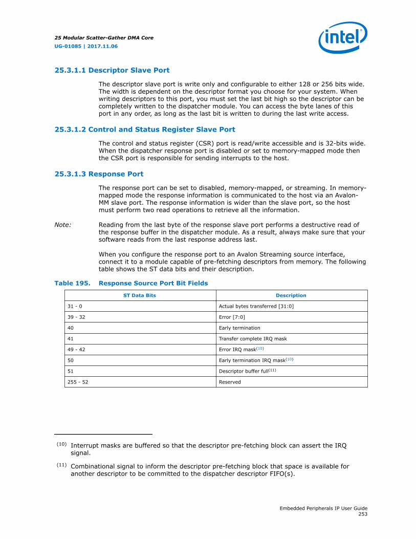
25.3.1.1 Descriptor Slave Port
The descriptor slave port is write only and configurable to either 128 or 256 bits wide.The width is dependent on the descriptor format you choose for your system. Whenwriting descriptors to this port, you must set the last bit high so the descriptor can becompletely written to the dispatcher module. You can access the byte lanes of thisport in any order, as long as the last bit is written to during the last write access.
25.3.1.2 Control and Status Register Slave Port
The control and status register (CSR) port is read/write accessible and is 32-bits wide.When the dispatcher response port is disabled or set to memory-mapped mode thenthe CSR port is responsible for sending interrupts to the host.
25.3.1.3 Response Port
The response port can be set to disabled, memory-mapped, or streaming. In memory-mapped mode the response information is communicated to the host via an Avalon-MM slave port. The response information is wider than the slave port, so the hostmust perform two read operations to retrieve all the information.
Note: Reading from the last byte of the response slave port performs a destructive read ofthe response buffer in the dispatcher module. As a result, always make sure that yoursoftware reads from the last response address last.
When you configure the response port to an Avalon Streaming source interface,connect it to a module capable of pre-fetching descriptors from memory. The followingtable shows the ST data bits and their description.
Table 195. Response Source Port Bit Fields
ST Data Bits Description
31 - 0 Actual bytes transferred [31:0]
39 - 32 Error [7:0]
40 Early termination
41 Transfer complete IRQ mask
49 - 42 Error IRQ mask(10)
50 Early termination IRQ mask(10)
51 Descriptor buffer full(11)
255 - 52 Reserved
(10) Interrupt masks are buffered so that the descriptor pre-fetching block can assert the IRQsignal.
(11) Combinational signal to inform the descriptor pre-fetching block that space is available foranother descriptor to be committed to the dispatcher descriptor FIFO(s).
25 Modular Scatter-Gather DMA Core
UG-01085 | 2017.11.06
Embedded Peripherals IP User Guide253
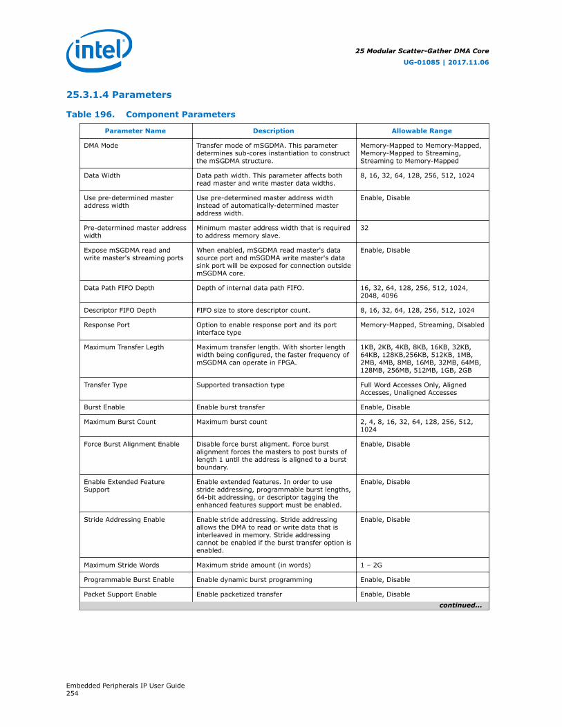
25.3.1.4 Parameters
Table 196. Component Parameters
Parameter Name Description Allowable Range
DMA Mode Transfer mode of mSGDMA. This parameterdetermines sub-cores instantiation to constructthe mSGDMA structure.
Memory-Mapped to Memory-Mapped,Memory-Mapped to Streaming,Streaming to Memory-Mapped
Data Width Data path width. This parameter affects bothread master and write master data widths.
8, 16, 32, 64, 128, 256, 512, 1024
Use pre-determined masteraddress width
Use pre-determined master address widthinstead of automatically-determined masteraddress width.
Enable, Disable
Pre-determined master addresswidth
Minimum master address width that is requiredto address memory slave.
32
Expose mSGDMA read andwrite master's streaming ports
When enabled, mSGDMA read master's datasource port and mSGDMA write master's datasink port will be exposed for connection outsidemSGDMA core.
Enable, Disable
Data Path FIFO Depth Depth of internal data path FIFO. 16, 32, 64, 128, 256, 512, 1024,2048, 4096
Descriptor FIFO Depth FIFO size to store descriptor count. 8, 16, 32, 64, 128, 256, 512, 1024
Response Port Option to enable response port and its portinterface type
Memory-Mapped, Streaming, Disabled
Maximum Transfer Legth Maximum transfer length. With shorter lengthwidth being configured, the faster frequency ofmSGDMA can operate in FPGA.
1KB, 2KB, 4KB, 8KB, 16KB, 32KB,64KB, 128KB,256KB, 512KB, 1MB,2MB, 4MB, 8MB, 16MB, 32MB, 64MB,128MB, 256MB, 512MB, 1GB, 2GB
Transfer Type Supported transaction type Full Word Accesses Only, AlignedAccesses, Unaligned Accesses
Burst Enable Enable burst transfer Enable, Disable
Maximum Burst Count Maximum burst count 2, 4, 8, 16, 32, 64, 128, 256, 512,1024
Force Burst Alignment Enable Disable force burst aligment. Force burstalignment forces the masters to post bursts oflength 1 until the address is aligned to a burstboundary.
Enable, Disable
Enable Extended FeatureSupport
Enable extended features. In order to usestride addressing, programmable burst lengths,64-bit addressing, or descriptor tagging theenhanced features support must be enabled.
Enable, Disable
Stride Addressing Enable Enable stride addressing. Stride addressingallows the DMA to read or write data that isinterleaved in memory. Stride addressingcannot be enabled if the burst transfer option isenabled.
Enable, Disable
Maximum Stride Words Maximum stride amount (in words) 1 – 2G
Programmable Burst Enable Enable dynamic burst programming Enable, Disable
Packet Support Enable Enable packetized transfer Enable, Disable
continued...
25 Modular Scatter-Gather DMA Core
UG-01085 | 2017.11.06
Embedded Peripherals IP User Guide254

Parameter Name Description Allowable Range
Note: When PACKET_ENABLE parameter isdisabled and TRANSFER_TYPE is not"Full Word Accesses Only", anyunaligned transfer length will causeadditional bytes to be written during thelast transfer beat of the Avalonstreaming data source port of the readmaster core. Only with this parameterset TRUE, actual bytes transferred ismeaningful for the transaction.PACKET_ENABLE only applys for ST-to-MM and MM-to-ST DMA operation mode.
Error Enable Enable error field of ST interface Enable, Disable
Error Width Error field width 1, 2, 3, 4, 5, 6, 7, 8
Channel Enable Enable channel field of ST interface Enable, Disable
Channel Width Channel field width 1, 2, 3, 4, 5, 6, 7, 8
Enable Pre-Fetching module Enables prefetcher modules, a hardware corewhich fetches descriptors from memory.
Enable, Disable
Enable bursting on descriptorread master
Enable read burst will turn on the burstingcapabilities of the prefetcher's read descriptorinterface.
Enable, Disable
Data Width of Descriptor read/write master data path
Width of the Avalon-MM descriptor read/writedata path.
32, 64, 128, 256
Maximum Burst Count ondescriptor read master
Maximum burst count. Enable, Disable
25 Modular Scatter-Gather DMA Core
UG-01085 | 2017.11.06
Embedded Peripherals IP User Guide255

25.3.2 mSGDMA Parameter Editor
Figure 71. Modular Scatter-Gather DMA Parameter Editor
25.4 mSGDMA Descriptors
The descriptor slave port is 128-bits for standard descriptors and 256-bits forextended descriptors. The tables below show acceptable standard and extendeddescriptor formats.
Table 197. Standard Descriptor Format
Byte Lanes
Offset 3 2 1 0
0x0 Read Address[31:0]
0x4 Write Address[31:0]
0x8 Length[31:0]
0xC Control[31:0]
25 Modular Scatter-Gather DMA Core
UG-01085 | 2017.11.06
Embedded Peripherals IP User Guide256
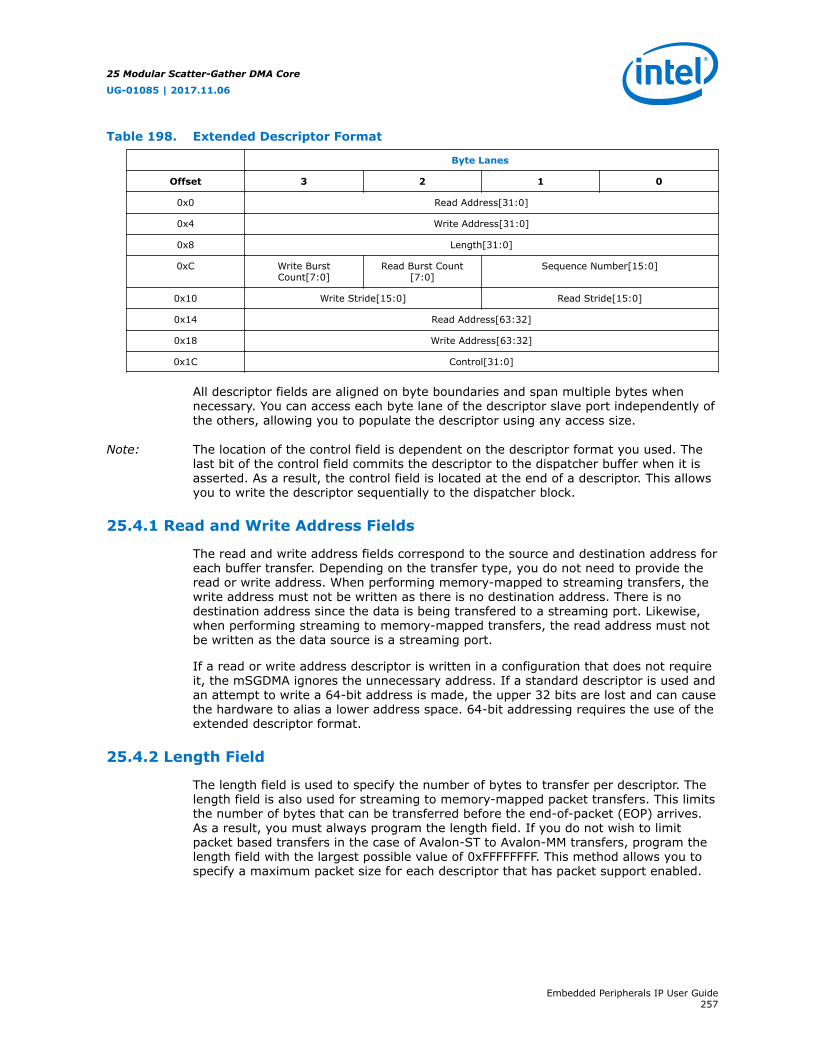
Table 198. Extended Descriptor Format
Byte Lanes
Offset 3 2 1 0
0x0 Read Address[31:0]
0x4 Write Address[31:0]
0x8 Length[31:0]
0xC Write BurstCount[7:0]
Read Burst Count[7:0]
Sequence Number[15:0]
0x10 Write Stride[15:0] Read Stride[15:0]
0x14 Read Address[63:32]
0x18 Write Address[63:32]
0x1C Control[31:0]
All descriptor fields are aligned on byte boundaries and span multiple bytes whennecessary. You can access each byte lane of the descriptor slave port independently ofthe others, allowing you to populate the descriptor using any access size.
Note: The location of the control field is dependent on the descriptor format you used. Thelast bit of the control field commits the descriptor to the dispatcher buffer when it isasserted. As a result, the control field is located at the end of a descriptor. This allowsyou to write the descriptor sequentially to the dispatcher block.
25.4.1 Read and Write Address Fields
The read and write address fields correspond to the source and destination address foreach buffer transfer. Depending on the transfer type, you do not need to provide theread or write address. When performing memory-mapped to streaming transfers, thewrite address must not be written as there is no destination address. There is nodestination address since the data is being transfered to a streaming port. Likewise,when performing streaming to memory-mapped transfers, the read address must notbe written as the data source is a streaming port.
If a read or write address descriptor is written in a configuration that does not requireit, the mSGDMA ignores the unnecessary address. If a standard descriptor is used andan attempt to write a 64-bit address is made, the upper 32 bits are lost and can causethe hardware to alias a lower address space. 64-bit addressing requires the use of theextended descriptor format.
25.4.2 Length Field
The length field is used to specify the number of bytes to transfer per descriptor. Thelength field is also used for streaming to memory-mapped packet transfers. This limitsthe number of bytes that can be transferred before the end-of-packet (EOP) arrives.As a result, you must always program the length field. If you do not wish to limitpacket based transfers in the case of Avalon-ST to Avalon-MM transfers, program thelength field with the largest possible value of 0xFFFFFFFF. This method allows you tospecify a maximum packet size for each descriptor that has packet support enabled.
25 Modular Scatter-Gather DMA Core
UG-01085 | 2017.11.06
Embedded Peripherals IP User Guide257
25.4.3 Sequence Number Field
The sequence number field is available only when using extended descriptors.Thesequence number is an arbitrary value that you assign to a descriptor, so that you candetermine which descriptor is being operated on by the read and write masters. Whenperforming memory-mapped to memory-mapped transfers, this value is trackedindependently for masters since each can be operating on a different descriptor. Touse this functionality, program the descriptors with unique sequence numbers. Then,access the dispatcher CSR slave port to determine which descriptor is operated on.
25.4.4 Read and Write Burst Count Fields
The programmable read and write burst counts are only available when using theextended descriptor format. The programmable burst count is optional and can bedisabled in the read and write masters. Because the programmable burst count is aneight bit field for each master, the maximum that you can program burst counts of 1to 128. Programming a value of zero or anything larger than 128 bits will be convertedto the maximum burst count specified for each master automatically.
The maximum programmable burst count is 128 but when you instantiate the DMA,you can have different selections up to 1024. Refer to the MAX_BURST_COUNTparameter in the parameter table. You will still have a burst count of 128 if youprogram for greater than 128. Programing to 0, gets the maximum burst countselected during instantiation time.
Related Links
Parameters on page 254For more information, refer to the MAX_BURST_COUNT parameter.
25.4.5 Read and Write Stride Fields
The read and write stride fields are optional and only available when using theextended descriptor format. The stride value determines how the read and writemasters increment the address when accessing memory. The stride value is in termsof words, so the address incrementing is dependent on the master data width.
When stride is enabled, the master defaults to sequential accesses, which is theequivalent to a stride distance of one. A stride of zero instructs the master tocontinuously access the same address. A stride of two instructs the master to skipevery other word in a sequential transfer. You can use this feature to performinterleaved data accesses, or to perform a frame buffer row and column transpose.The read and write stride distances are stored independently allowing, you to usedifferent address incrementing for read and write accesses in memory-to-memorytransfers. For example, to perform a 2:1 data decimation transfer, you would simplyconfigure the read master for a stride distance of two and the write master for a stridedistance of one. To complete the decimation operation you could also insert a filterbetween the two masters.
25.4.6 Control Field
The control field is available for both the standard and extended descriptor formats.This field can be programmed to configure parked descriptors, error handling, andinterrupt masks. The interrupt masks are programmed into the descriptor so thatinterrupt enables are unique for each transfer.
25 Modular Scatter-Gather DMA Core
UG-01085 | 2017.11.06
Embedded Peripherals IP User Guide258

Table 199. Descriptor Control Field Bit Definition
Bit Sub-Field Name Definition
31 Go Commits all the descriptor information into the descriptor FIFO.As the host writes different fields in the descriptor, FIFO byte enablesare asserted to transfer the write data to appropriate byte locations inthe FIFO.However, the data written is not committed until the go bit has beenwritten.As a result, ensure that the go bit is the last bit written for eachdescriptor.Writing '1' to the go bit commits the entire descriptor into thedescriptor FIFO(s).
30:25 <reserved>
24 Early done enable Hides the latency between read descriptors.When the read master is set, it does not wait for pending reads toreturn before requesting another descriptor.Typically this bit is set for all descriptors except the last one. This bit ismost effective for hiding high read latency. For example, it reads fromSDRAM, PCIe, and SRIO.
23:16 Transmit Error / Error IRQEnable
For for Avalon-MM to Avalon-ST transfers, this field is used to specify atransmit error.This field is commonly used for transmitting error informationdownstream to streaming components, such as an Ethernet MAC.In this mode, these control bits control the error bits on the streamingoutput of the read master.For Avalon-ST to Avalon-MM transfers, this field is used as an errorinterrupt mask.As errors arrive at the write master streaming sink port, they are heldpersistently. When the transfer completes, if any error bits were set atany time during the transfer and the error interrupt mask bits are set,then the host receives an interrupt.In this mode, these control bits are used as an error encounteredinterrupt enable.
15 Early Termination IRQ Enable Signals an interrupt to the host when a Avalon-ST to Avalon-MMtransfer completes early.For example, if you set this bit and set the length field to 1MB forAvalon-ST to Avalon-MM transfers, this interrupt asserts when morethan 1MB of data arrives to the write master without the end of packetbeing seen.
14 Transfer Complete IRQ Enable Signals an interrupt to the host when a transfer completes.In the case of Avalon-MM to Avalon-ST transfers, this interrupt is basedon the read master completing a transfer.In the case of Avalon-ST to Avalon-MM or Avalon-MM to Avalon-MMtransfers, this interrupt is based on the write master completing atransfer.
13 <reserved>
12 End on EOP End on end of packet allows the write master to continuously transferdata during Avalon-ST to Avalon-MM transfers without knowing howmuch data is arriving ahead of time.This bit is commonly set for packet-based traffic such as Ethernet.
11 Park Writes When set, the dispatcher continues to reissue the same descriptor tothe write master when no other descriptors are buffered.
10 Park Reads When set, the dispatcher continues to reissue the same descriptor tothe read master when no other descriptors are buffered. This iscommonly used for video frame buffering.
continued...
25 Modular Scatter-Gather DMA Core
UG-01085 | 2017.11.06
Embedded Peripherals IP User Guide259
Bit Sub-Field Name Definition
9 Generate EOP Emits an end of packet on last beat of a Avalon-MM to Avlaon-STtransfer
8 Generate SOP Emits a start of packet on the first beat of a Avalon-MM to Avalon-STtransfer
7:0 Transmit Channel Emits a channel number during Avalon-MM to Avalon-ST transfers
25.5 Programming Model
25.5.1 Stop DMA Operation
The stop DMA operation is also referring to stop dispatcher. Once the “StopDispatcher” bit is set in the Control Register, no further new read or write transactionis issued. However, existing transactions pending completion are allowed to complete.The command buffer in both the read master and write master must be clear beforethe DMA resumes operation via a reset request. Proceed with the follwing steps for thestop DMA operation:
1. Set the “Stop Dispatcher” bit of the Control Register.
2. Recursively check if “Stopped” bit of Status Register is asserted.
3. When the “Stopped” bit of the Status Register is asserted, reset the DMA bysetting the “Reset Dispatcher” bit of the Control Register.
4. Check if the “Resetting” bit of the Status Register is deasserted. If it is, DMA isnow back in normal operation.
25.5.2 Stop Descriptor Operation
The Stop Descriptor temporary stops the dispatcher core from continuing to issuecommands to the read master and write master. The dispatcher core operates in thesense that it can accept a descriptor sent by the host up to its descriptor FIFO limit.Proceed with the follwing steps for the stop descriptor operation:
1. Set “Stop Descriptor” bit of Control Register.
2. Check if “Stopped” bit of Status Register is asserted.
To resume DMA from its previously stop descriptor operation, do the following:
1. Unset the “Stop Descriptor” bit of Control Register.
2. Check if “Stopped” bit of Status Register is deasserted.
25.5.3 Recovery from Stopped on Error and Stopped on Early Termination
When stopped on error or stopped on early termination occurs, mSGDMA requires asoftware reset to continue operation.
1. When the “Stopped” bit of the Status register is asserted, reset the DMA bysetting the “Reset Dispatcher” bit of Control register.
2. Check if the “Resetting” bit of Status register is deasserted. If it is, DMA is nowback in normal operation.
25 Modular Scatter-Gather DMA Core
UG-01085 | 2017.11.06
Embedded Peripherals IP User Guide260
25.6 Register Map of mSGDMA
The following table illustrates the mSGDMA register map under observation by hostprocessor from its Avalon-MM CSR interfaces.
Table 200. CSR Registers Map
Byte Lanes
Offset Attribute 3 2 1 0
0x0 Read/Clear Status
0x4 Read/Write Control
0x8 Read Write Fill Level[15:0] Read Fill Level[15:0]
0xC Read <reserved>(12) Response Fill Level[15:0]
0x10 Read Write Sequence Number[15:0](13) Read Sequence Number[15:0]2
0x14 N/A <reserved>1
0x18 N/A <reserved>1
0x1C N/A <reserved>1
25.6.1 Status Register
Table 201. Status Register Bit Definition
Bit Name Description
31:10
<reserved> N/A
9 IRQ Set when interrupt condition occurs.This bit is set by hardware and cleared by software. To clear this bit, software needs to writea 1 to this bit. This bit is set when a hardware event has a higher priority than a clear by asoftware event.
8 Stopped on EarlyTermination
When the dispatcher is programmed to stop on early termination, this bit is set. Also set,when the write master is performing a packet transfer and does not receive EOP before thepre-determined amount of bytes are transferred, which is set in the descriptor length field.If you do not wish to use early termination you should set the transfer length of thedescriptor to 0xFFFFFFFF ,which gives you the maximum packet based transfer possible(early termination is always enabled for packet transfers).
7 Stopped on Error When the dispatcher is programmed to stop errors and when an error beat enters the writemaster the bit is set.
6 Resetting Set when you write to the software reset register and the SGDMA is in the middle of a resetcycle. This reset cycle is necessary to make sure there are no incoming transfers on thefabric. When this bit de-asserts you may start using the SGDMA again.
5 Stopped Set when you either manually stop the SGDMA, or you setup the dispatcher to stop onerrors or early termination and one of those conditions occurred. If you manually stop theSGDMA this bit is asserted after the master completes any read or write operations thatwere already in progress.
continued...
(12) Writing to reserved bits will have no impact on the hardware, reading will return unknowndata.
(13) Sequence numbers will only be present when dispatcher enhanced features are enabled.
25 Modular Scatter-Gather DMA Core
UG-01085 | 2017.11.06
Embedded Peripherals IP User Guide261
Bit Name Description
4 Response Buffer Full Set when the response buffer is full.
3 Response BufferEmpty
Set when the response buffer is empty.
2 Descriptor Buffer Full Set when either the read or write command buffers are full.
1 Descriptor BufferEmpty
Set when both the read and write command buffers are empty.
0 Busy Set when the dispatcher still has commands buffered, or one of the masters is stilltransferring data.
25.6.2 Control Register
Table 202. Control Register Bit Definition
Bit Name Description
31:10
<reserved> N/A
5 Stop Descriptors Setting this bit stops the SGDMA dispatcher from issuing more descriptors to the read orwrite masters. Read the stopped status register to determine when the dispatcher stoppedissuing commands and the read and write masters are idle.
4 Global InterruptEnable Mask
Setting this bit allows interrupts to propagate to the interrupt sender port. This mask occursafter the register logic so that interrupts are not missed when the mask is disabled.
3 Stop on EarlyTermination
Setting this bit stops the SGDMA from issuing more read/write commands to the mastermodules if the write master attempts to write more data than the user specifies in thelength field for packet transactions. The length field is used to limit how much data can besent and is always enabled for packet based writes.
2 Stop on Error Setting this bit stops the SGDMA from issuing more read/write commands to the mastermodules if an error enters the write master module sink port.
1 Reset Dispatcher Setting this bit resets the registers and FIFOs of the dispatcher and master modules. Sinceresets can take multiple clock cycles to complete due to transfers being in flight on thefabric, you should read the resetting status register to determine when a full reset cycle hascompleted.
0 Stop Dispatcher Setting this bit stops the SGDMA in the middle of a transaction. If a read or write operationis occurring, then the access is allowed to complete. Read the stopped status register todetermine when the SGDMA has stopped. After reset, the dispatcher core defaults to a startmode of operation.
The response slave port of mSGDMA contains registers providing information of theexecuted transaction. This register map is only applicable when the response mode isenabled and set to memory mapped. Also when the response port is enabled, it needsto have responses read because it buffers responses. When setup as a memory-mapped slave port, reading byte offset 0x7 outputs the response. If the response FIFObecomes full the dispatcher stops issuing transfer commands to the read and writemasters. The following describes the registers definition.
25 Modular Scatter-Gather DMA Core
UG-01085 | 2017.11.06
Embedded Peripherals IP User Guide262

Table 203. Response Registers Map
Byte Lanes
Offset Access 3 2 1 0
0x0 Read Actual Bytes Transferred[31:0]
0x4 Read <reserved>(14) <reserved> EarlyTermination(15)
Error[7:0]
The following list explains each of the fields:
• Actual bytes transferred determines how many bytes transferred when themSGDMA is configured in Avalon-ST to Avlaon-MM mode with packet supportenabled. Since packet transfers are terminated by the IP providing the data, thisfield counts the number of bytes between the start-of-packet (SOP) and end-of-packet (EOP) received by the write master. If the early termination bit of theresponse is set, then the actual bytes transferred is an underestimate if thetransfer is unaligned.
• Error Determines if any errors were issued when the mSGDMA is configured inAvalon-ST to Avlaon-MM mode with error support enabled. Each error bit ispersistent so that errors can accumulate throughout the transfer.
• Early Termination determines if a transfer terminates because the transferlength is exceeded when the SGDMA is configured in Avalon-ST to Avalon-MMmode with packet support enabled. This bit is set when the number of bytestransferred exceeds the transfer length set in the descriptor before the end-of-packet is received by the write master.
(14) Reading from byte 7 outputs the response FIFO.
(15) Early Termination is a single bit located at bit 8 of offset 0x4.
25 Modular Scatter-Gather DMA Core
UG-01085 | 2017.11.06
Embedded Peripherals IP User Guide263
25.7 Modular Scatter-Gather DMA Prefetcher Core
The mSGDMA Prefetcher core is an additional micro core to the existing mSGDMAcore. The Prefetcher core provides extra functionality through the Avalon-MM anddispatcher core. The Avalon-MM fetches a series of descriptors from memory thatdescribes the required data transfers before passing them to dispatcher core for datatransfer execution. The series of descriptors in memory can be linked together to forma descriptor list. This allows the DMA core to execute multiple descriptors in singlerun, thus enabling transfer to a non-contiguous memory space and improves systemperformance.
25.7.1 Functional Description
25.7.1.1 Supported Features
• Descriptor linked list
• Data transfer to non-contiguous memory space
• Descriptor write back
• Hardware descriptor polling
• 64-bit address spaces
25.7.1.2 Architecture Overview
The Prefetcher core supports all the three existing Modular SGDMA configurations:
• Memory-Mapped to Memory-Mapped
• Memory-Mapped to Streaming
• Streaming to Memory-Mapped
On interfaces facing host and external peripherals, it has dedicated Avalon-MM readand write master interfaces to fetch series of descriptors from memory as well asperforming a descriptor write back. It has one Avalon Memory-Mapped CSR slaveinterface for the host processor to access the configuration register in the Prefetchercore.
On interfaces facing the internal dispatcher core, it has an Avalon-MM descriptor writemaster interface to write a descriptor to the dispatcher core. It has Avalon-STresponse sink interface to receive response information from the dispatcher core uponcompletion of each descriptor execution.
25 Modular Scatter-Gather DMA Core
UG-01085 | 2017.11.06
Embedded Peripherals IP User Guide264

Figure 72. Memory-Mapped to Memory-Mapped Configuration with Prefetcher Enabled
Read MasterM
SRC
SRC
SNK
Write MasterM
SRC
SNK
SNK
Dispatcher
S
SNK SRC
SNK
SRC
SNK SRC
Read Response Read Command
Write Response Write Command
ST Data
MM Read Data
MM Write Data
Prefetcher
S
M
M SNK
SRC
Host
Descriptors
Response
CSR
CSR
MM Read Descriptors
MM Write Descriptors
IRQ
Figure 73. Memory-Mapped to Streaming Configuration with Prefetcher Enabled
Read MasterM
SRC
SRC
SNK
Dispatcher
S
SNK SRC
SNK
SRC
Read Response Read Command
MM Read Data
Prefetcher
S
M
M SNK
SRC
Host
Descriptors
Response
CSR
CSR
MM Read Descriptors
MM Write Descriptors
ST Data
IRQ
25 Modular Scatter-Gather DMA Core
UG-01085 | 2017.11.06
Embedded Peripherals IP User Guide265
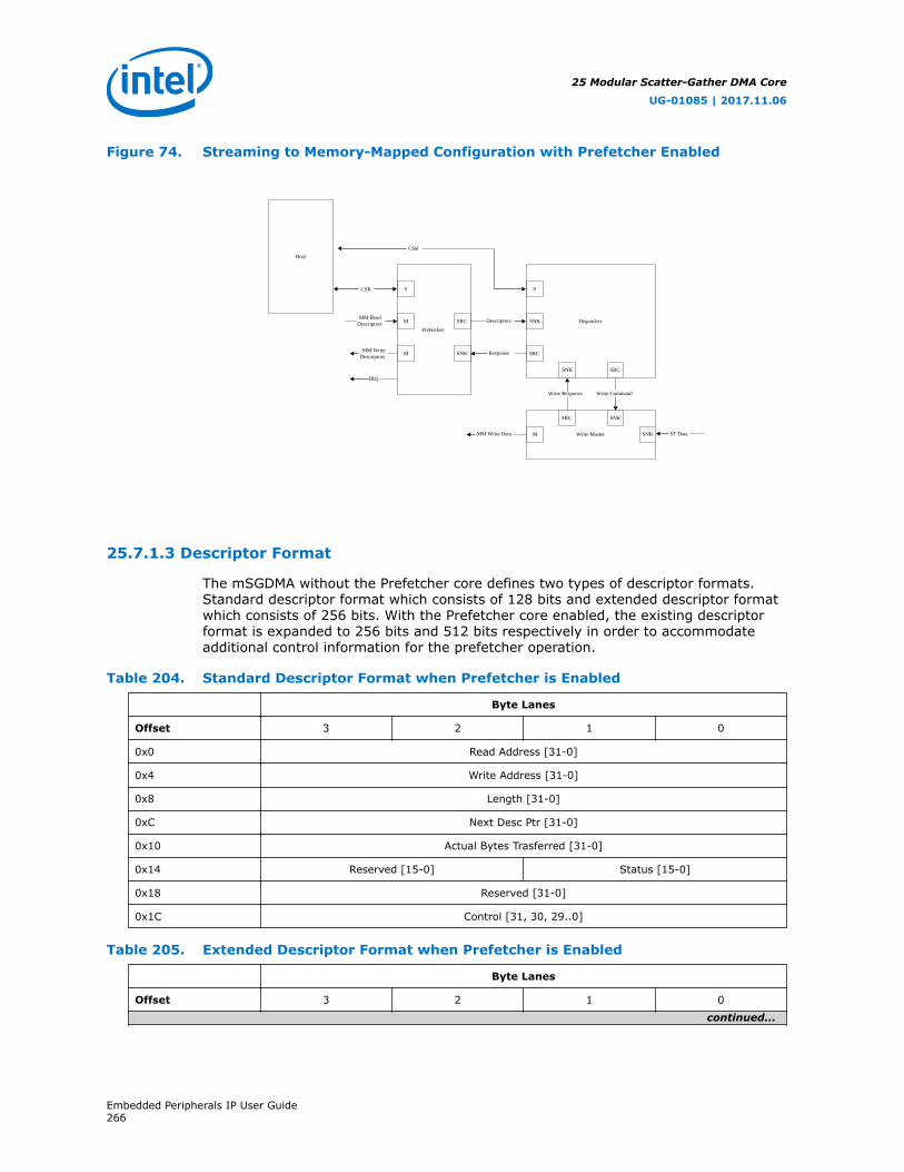
Figure 74. Streaming to Memory-Mapped Configuration with Prefetcher Enabled
Write MasterM
SRC
SNK
SNK
Dispatcher
S
SNK
SRC
SNK SRC
Write Response Write Command
MM Write Data
Prefetcher
S
M
M SNK
SRC
Host
Descriptors
Response
CSR
CSR
MM Read Descriptors
MM Write Descriptors
ST Data
IRQ
25.7.1.3 Descriptor Format
The mSGDMA without the Prefetcher core defines two types of descriptor formats.Standard descriptor format which consists of 128 bits and extended descriptor formatwhich consists of 256 bits. With the Prefetcher core enabled, the existing descriptorformat is expanded to 256 bits and 512 bits respectively in order to accommodateadditional control information for the prefetcher operation.
Table 204. Standard Descriptor Format when Prefetcher is Enabled
Byte Lanes
Offset 3 2 1 0
0x0 Read Address [31-0]
0x4 Write Address [31-0]
0x8 Length [31-0]
0xC Next Desc Ptr [31-0]
0x10 Actual Bytes Trasferred [31-0]
0x14 Reserved [15-0] Status [15-0]
0x18 Reserved [31-0]
0x1C Control [31, 30, 29..0]
Table 205. Extended Descriptor Format when Prefetcher is Enabled
Byte Lanes
Offset 3 2 1 0
continued...
25 Modular Scatter-Gather DMA Core
UG-01085 | 2017.11.06
Embedded Peripherals IP User Guide266
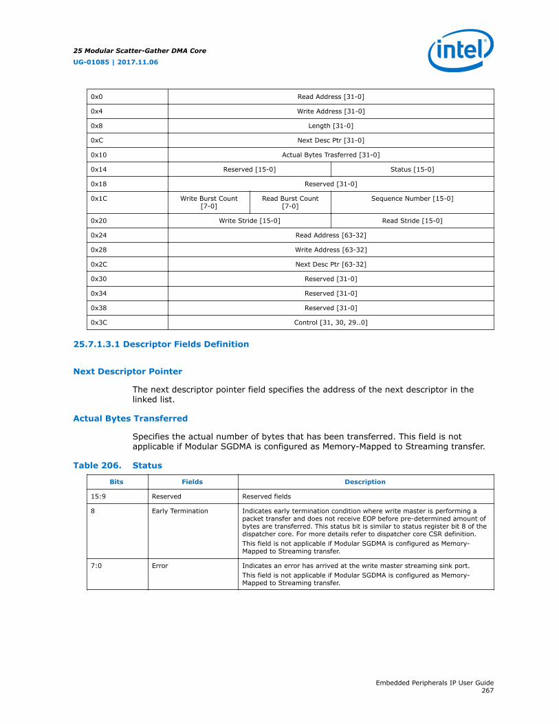
0x0 Read Address [31-0]
0x4 Write Address [31-0]
0x8 Length [31-0]
0xC Next Desc Ptr [31-0]
0x10 Actual Bytes Trasferred [31-0]
0x14 Reserved [15-0] Status [15-0]
0x18 Reserved [31-0]
0x1C Write Burst Count[7-0]
Read Burst Count[7-0]
Sequence Number [15-0]
0x20 Write Stride [15-0] Read Stride [15-0]
0x24 Read Address [63-32]
0x28 Write Address [63-32]
0x2C Next Desc Ptr [63-32]
0x30 Reserved [31-0]
0x34 Reserved [31-0]
0x38 Reserved [31-0]
0x3C Control [31, 30, 29..0]
25.7.1.3.1 Descriptor Fields Definition
Next Descriptor Pointer
The next descriptor pointer field specifies the address of the next descriptor in thelinked list.
Actual Bytes Transferred
Specifies the actual number of bytes that has been transferred. This field is notapplicable if Modular SGDMA is configured as Memory-Mapped to Streaming transfer.
Table 206. Status
Bits Fields Description
15:9 Reserved Reserved fields
8 Early Termination Indicates early termination condition where write master is performing apacket transfer and does not receive EOP before pre-determined amount ofbytes are transferred. This status bit is similar to status register bit 8 of thedispatcher core. For more details refer to dispatcher core CSR definition.This field is not applicable if Modular SGDMA is configured as Memory-Mapped to Streaming transfer.
7:0 Error Indicates an error has arrived at the write master streaming sink port.This field is not applicable if Modular SGDMA is configured as Memory-Mapped to Streaming transfer.
25 Modular Scatter-Gather DMA Core
UG-01085 | 2017.11.06
Embedded Peripherals IP User Guide267

Table 207. Control
Bits Fields Description
30 Owned by Hardware This field determines whether hardware or software has write access to thecurrent descriptor.When this field is set to 1, the Modular SGDMA can update the descriptorand software should not access the descriptor due to the possibility of raceconditions. Otherwise, it is safe for software to update the descriptor.
For bit 31 and 29:0, refer to descriptor control field bit 31 and 29:0 defined indispatcher core. Table 199 on page 259
25.7.1.3.2 Descriptor Processing
The DMA descriptors specify data transfers to be performed. With the Prefetcher core,a descriptor is stored in memory and accessed by the Prefetcher core through itsdescriptor write and descriptor read Avalon-MM master. The mSGDMA has an internalFIFO to store descriptors read from memory. This FIFO is located in the dispatcher’score. The descriptors must be initialized and aligned on a descriptor read/write datawidth boundary. The Prefetcher core relies on a cleared Owned By Hardware bit tostop processing. When the Owedn by Hardware bit is 1, the Prefetcher core goesahead to process the descriptor. When the Owned by Hardware bit is 0, the Prefetchercore does not process the current descriptor and assumes the linked list has ended orthe next descriptor linked list is not yet ready.
Each time a descriptor has been processed, the core updates the Actual ByteTransferred, Status and Control fields of the descriptor in memory (descriptor writeback). The Owned by Hardware bit in the descriptor control field is cleared by the coreduring descriptor write back. Refer to software programming model section to knowmore about recommended way to set up the Prefetcher core, building and updatingthe descriptor list.
In order for the Prefetcher to know which memory addresses to perform descriptorwrite back, the next descriptor pointer information will need to be buffered inPrefetcher core. This buffer depth will be similar to descriptor FIFO depth in dispatchercore. This information is taken out from buffer each time a response is received fromdispatcher.
25.7.1.4 Registers
25.7.1.4.1 Register Map
25 Modular Scatter-Gather DMA Core
UG-01085 | 2017.11.06
Embedded Peripherals IP User Guide268
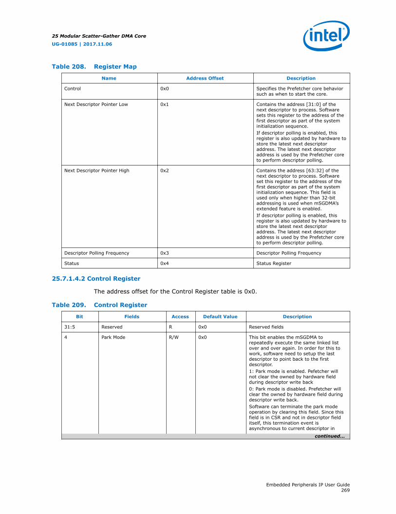
Table 208. Register Map
Name Address Offset Description
Control 0x0 Specifies the Prefetcher core behaviorsuch as when to start the core.
Next Descriptor Pointer Low 0x1 Contains the address [31:0] of thenext descriptor to process. Softwaresets this register to the address of thefirst descriptor as part of the systeminitialization sequence.If descriptor polling is enabled, thisregister is also updated by hardware tostore the latest next descriptoraddress. The latest next descriptoraddress is used by the Prefetcher coreto perform descriptor polling.
Next Descriptor Pointer High 0x2 Contains the address [63:32] of thenext descriptor to process. Softwareset this register to the address of thefirst descriptor as part of the systeminitialization sequence. This field isused only when higher than 32-bitaddressing is used when mSGDMA’sextended feature is enabled.If descriptor polling is enabled, thisregister is also updated by hardware tostore the latest next descriptoraddress. The latest next descriptoraddress is used by the Prefetcher coreto perform descriptor polling.
Descriptor Polling Frequency 0x3 Descriptor Polling Frequency
Status 0x4 Status Register
25.7.1.4.2 Control Register
The address offset for the Control Register table is 0x0.
Table 209. Control Register
Bit Fields Access Default Value Description
31:5 Reserved R 0x0 Reserved fields
4 Park Mode R/W 0x0 This bit enables the mSGDMA torepeatedly execute the same linked listover and over again. In order for this towork, software need to setup the lastdescriptor to point back to the firstdescriptor.1: Park mode is enabled. Pefetcher willnot clear the owned by hardware fieldduring descriptor write back0: Park mode is disabled. Prefetcher willclear the owned by hardware field duringdescriptor write back.Software can terminate the park modeoperation by clearing this field. Since thisfield is in CSR and not in descriptor fielditself, this termination event isasynchronous to current descriptor in
continued...
25 Modular Scatter-Gather DMA Core
UG-01085 | 2017.11.06
Embedded Peripherals IP User Guide269

Bit Fields Access Default Value Description
progress (user can’t deterministicallychoose which descriptor in the linked listto stop).Park mode feature is not intended to beused on the fly. User must not enable thisbit when the Prefetcher is already inoperation. This bit shall be set duringinitialization/configuration phase of thecontrol register.
3 Global Interrupt EnableMask
R/W 0x0 Setting this bit will allow interrupts topropagate to the interrupt sender port.This mask occurs after the register logicso that interrupts are not missed when themask is disabled.Note: There is an equivalent global
interrupt enable mask bit indispatcher core CSR. When thePrefetcher is enabled, softwareshall use this bit. When thePrefetcher is disabled, softwareshall use equivalent globalinterrupt enable mask bit indispatcher core CSR.
2 Reset_Prefetcher R/W1S(16) 0x0 This bit is used when software intends tostop the Prefetcher core when it is in themiddle of data transfer. When this bit is 1,the Prefetcher core begin its resetsequence.This bit is automatically cleared byhardware when the reset sequence hascompleted. Therefore, software need topoll for this bit to be cleared by hardwareto ensure the reset sequence has finished.This function is intended to be used alongwith reset dispatcher function indispatcher core. Once the reset sequencein the Prefetcher core has completed,software is expected to reset thedispatcher core, polls for dispatcher’sreset sequence to be completed byreading dispatcher core status register.
1 Desc_Poll_En R/W 0x0 Descriptor polling enable bit.1: When the last descriptor in currentlinked list has been processed, thePrefetcher core polls the Owned ByHardware bit of next descriptor to be setand automatically resumes data transferwithout the need for software to set theRun bit. The polling frequency is specifiedin Desc_Poll_Freq register.0: When the last descriptor in currentlinked list has been processed, thePrefetcher stops operation and clears therun bit. In order to restart the DMAengine, software need to set the Run bitback to 1.In case software intends to disable pollingoperation in the middle of transfer,software can write this field to 0. In thiscase, the whole mSGDMA operation isstopped when the Prefetcher coreencounter owned by hardware bit = 0.
continued...
25 Modular Scatter-Gather DMA Core
UG-01085 | 2017.11.06
Embedded Peripherals IP User Guide270
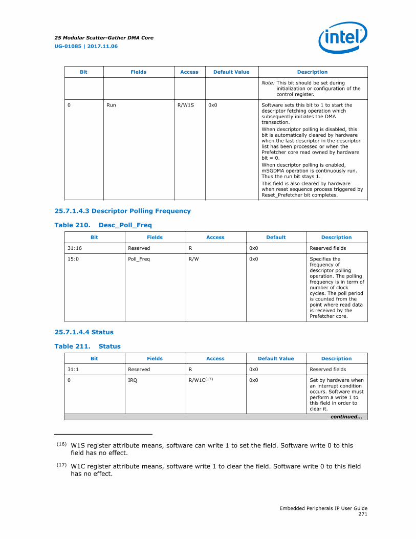
Bit Fields Access Default Value Description
Note: This bit should be set duringinitialization or configuration of thecontrol register.
0 Run R/W1S 0x0 Software sets this bit to 1 to start thedescriptor fetching operation whichsubsequently initiates the DMAtransaction.When descriptor polling is disabled, thisbit is automatically cleared by hardwarewhen the last descriptor in the descriptorlist has been processed or when thePrefetcher core read owned by hardwarebit = 0.When descriptor polling is enabled,mSGDMA operation is continuously run.Thus the run bit stays 1.This field is also cleared by hardwarewhen reset sequence process triggered byReset_Prefetcher bit completes.
25.7.1.4.3 Descriptor Polling Frequency
Table 210. Desc_Poll_Freq
Bit Fields Access Default Description
31:16 Reserved R 0x0 Reserved fields
15:0 Poll_Freq R/W 0x0 Specifies thefrequency ofdescriptor pollingoperation. The pollingfrequency is in term ofnumber of clockcycles. The poll periodis counted from thepoint where read datais received by thePrefetcher core.
25.7.1.4.4 Status
Table 211. Status
Bit Fields Access Default Value Description
31:1 Reserved R 0x0 Reserved fields
0 IRQ R/W1C(17) 0x0 Set by hardware whenan interrupt conditionoccurs. Software mustperform a write 1 tothis field in order toclear it.
continued...
(16) W1S register attribute means, software can write 1 to set the field. Software write 0 to thisfield has no effect.
(17) W1C register attribute means, software write 1 to clear the field. Software write 0 to this fieldhas no effect.
25 Modular Scatter-Gather DMA Core
UG-01085 | 2017.11.06
Embedded Peripherals IP User Guide271

Bit Fields Access Default Value Description
There is an equivalentIRQ status bit in thedispatcher core CSR.When the Prefetcher isenabled, softwareuses this bit as an IRQstatus indication.When the Prefetcher isdisabled, softwareuses equivalent IRQstatus bit indispatcher core CSR.
25.7.1.5 Interfaces
25.7.1.5.1 Avalon-MM Read Descriptor
This interface is used to fetch descriptors in memory. It supports non-burst or burstmode which configurable during generation time.
Table 212. Avalon-MM Read Descriptor
Signal Role Width Description
Address 32 to 64-bit Avalon-MM read address.32-bits if extended feture is disabled.32- to 64-bits if extended feature isenabled.
Read 1 Avalon-MM read control
Read data 32, 64, 128, 256, 512 Avalon-MM read data bus. Data widthis configurable during IP generation.
Wait request 1 Avalon-MM wait request forbackpressure control.
Read data valid 1 Avalon-MM read data valid indication.
Burstcount 1/2/3/4/5 Avalon-MM burst count. The maximumburst count is configurable during IPgeneration.This signal role is applicable only whenthe Enable Bursting on the descriptorread master is turned on.
25.7.1.5.2 Avalon-MM Write Descriptor
This interface is used to access the Prefetcher CSR registers. It has fixed write andread wait time of 0 cycles and read latency of 1 cycle.
Table 213. Avalon-MM Write Descriptor
Signal Role Width Description
Address 32 to 64 Avalon-MM write address
Write 1 Avalon-MM read control
continued...
25 Modular Scatter-Gather DMA Core
UG-01085 | 2017.11.06
Embedded Peripherals IP User Guide272

Signal Role Width Description
Wait request 1 Avalon-MM waitrequest forbackpressure control
Write data 32, 64, 128, 256, 512 Avalon-MM write data bus
Byte enable 4, 8, 16, 32, 64 Avalon-MM write byte enable control.Its width is automatically derived fromselected data width
25.7.1.5.3 Avalon-MM CSR
This interface is used to access the Prefetcher CSR registers. It has fixed write andread wait time of 0 cycles and read latency of 1 cycle.
Table 214. Avalon-MM CSR
Signal Role Width Description
Address 3 Avalon-MM write address
Write 1 Avalon-MM read control
Read 1 Avalon-MM write control
Write data 32 Avalon-MM write data bus
Read data 32 Avalon-MM read data bus
25.7.1.5.4 Avalon-ST Descriptor Source
This interface is used by the Prefetcher to write descriptor information into thedispatcher core.
Table 215. Avalon-ST Descriptor Source
Signal Role Width Description
Valid 1 Avalon-ST valid control
Ready 1 Avalon-ST ready control with readylatency of 0. Refer to dispatcher'sdescriptor format for wrtie datadefinition.
Data 128/256 Avalon-ST data bus
25.7.1.5.5 Avalon-ST Response
This interface is used by the Prefetcher core to retrieve response information fromdispatcher’s core upon each transfer completion.
Table 216. Avalon-ST Response
Signal Role Width Description
Valid 1 Avalon-ST valid control.
continued...
25 Modular Scatter-Gather DMA Core
UG-01085 | 2017.11.06
Embedded Peripherals IP User Guide273
Signal Role Width Description
Prefetcher core expects valid signal toremain high while the bus is beingback pressured.
Ready 1 Avalon-ST ready control. Used by thePrefetcher core to back pressure theexternal ST response source.
Data 256 Avalon-ST data bus. Refer todispatcher’s response source format forST data definition.Prefetcher core expects data signals toremain constant while the bus is beingback pressured.
Streaming interface (ST) data bus format and definition are similar to the dispatcher’sresponse source format:
Table 217. Avalon-ST Response Data Format and Definition
Bits Signal Information
[31:0] Acutal bytes transferred [31:0]
[39:32] Error [7:0]
40 Early termination
41 Transfer complete IRQ mask
[49:42] Error IRQ mask
50 Early termination IRQ mask
51 Descriptor buffer full
[255:52] Reserved
25.7.1.5.6 IRQ Interface
When the Prefetcher is enabled, IRQ generation no longer outputs from thedispatcher’s core. It will be outputted from the Prefetcher core. The sources of theinterrupt remain the same which are transfer completion, early termination, and errordetection. Masking bits for each of the interrupt sources are programmed in thedescriptor. This information will be passed to the Prefetcher core through the STresponse interface. An equivalent global interrupt enable mask and IRQ status bitwhich are defined in dispatcher core are now defined in the Prefetcher core as well.These two bits need to be defined in the Prefetcher core since the actual IRQ registeris now located in the Prefetcher core.
25.7.1.6 Software Programming Model
25 Modular Scatter-Gather DMA Core
UG-01085 | 2017.11.06
Embedded Peripherals IP User Guide274
25.7.1.6.1 Setting up Descriptor and mSGDMA Configuration Flow
The following is the recommended software flow to setup the descriptor andconfiguring the mSGDMA.
1. Build the descriptor list and terminate the list with a non-hardware owneddescriptor (Owned By Hardware = 0).
2. Configure mSGDMA by accessing dispatcher core control register (for example: toconfigure Stop on Error, Stop on Early Termination, etc…)
3. Configure mSGDMA by accessing the Prefetcher core configuration register (forexample: to write the address of the first descriptor in the first list to the nextdescriptor pointer register and set the Run bit to 1 to initiate transfers).
4. While the core is processing the first list, your software may build a second list ofdescriptors.
5. An IRQ can be generated each time a descriptor transfer is completed (dependswhether transfer complete IRQ mask is set for that particular descriptor). If youonly need an IRQ to be generated when mSGDMA finishes processing the first list,you only need to set transfer complete IRQ mask for the last descriptor in the firstlist.
6. When the last descriptor in the first linked list has been processed, an IRQ will begenerated if the descriptor polling is disabled. Following this, your software needsto update the next descriptor pointer register with the address of the firstdescriptor in the second linked list before setting the run bit back to 1 to resumetransfers. If descriptor polling is enabled, software does not need to update thenext descriptor pointer register (for second descriptor linked list onwards) and setthe run bit back to 1. These 2 steps are automatically done by hardware. Theaddress of the new list is indicated by next descriptor pointer fields of the previouslist. The Prefetcher core polls for the Owned by Hardware bit to be 1 in order toresume transfers. Software only needs to flip the Owned by Hardware bit of thefirst descriptor in second linked list to 1 to indicate to the Prefetcher core that thesecond linked list is ready.
7. If there are new descriptors to add, always add them to the list which the core isnot processing (indicated by Owned By Hardware = 0). For example, if the core isprocessing the first list, add new descriptors to the second list and so forth. Thismethod ensures that the descriptors are not updated when the core is processingthem. Your software can read the descriptor in the memory to know the status ofthe transfer (for example; to know the actual bytes being transferred, any error inthe transfer).
25.7.1.6.2 Resetting Prefetcher Core Flow
The following is the recommended flow for software to stop the mSGDMA when it is inthe middle of operation.
1. Write 1 to the Prefetcher control register bit 2 (Reset_Prefetcher bit set to 1).
2. Poll for control register bit 2 to be 0 (Reset_Prefetcher bit cleared by hardware).
3. Trigger software reset condition in the dispatcher core.
4. Poll for software reset condition in the dispatcher core to be completed by readingthe dispatcher core status register.
5. The whole reset flow has completed, software can reconfigure the mSGDMA.
25 Modular Scatter-Gather DMA Core
UG-01085 | 2017.11.06
Embedded Peripherals IP User Guide275

25.7.1.7 Parameters
Table 218. Prefetcher Parameters
Name Legal Value Description
Enable Pre-fetching Module 1 or 0 1: Pre-fetching is enabled0: Pre-fetching is disabled
Enable bursting on descriptor readmaster
1 or 0 1: Pre-fetching module uses Avalon-MM bursting when fetching descriptors.
Data Width (Avalon-MM Read/WriteDescriptor)
32, 64, 128, 256, 512 Specifies the read and write data widthof Avalon-MM read and write descriptormaster.
Maximum Burst Count (Avalon-MMRead Descriptor)
1, 2, 4, 8, 16 Specifies the maximum read burstcount of Avalon-MM read descriptormaster.
Enable Extended Feature Support 1 or 0 This is a derived parameter from themSGDMA top level composed. This isneeded by this core to determinedescriptor length (different length forstandard/extended descriptor).
FIFO Depth 8, 16, 32, 64, 128, 256, 512, 1024 This is a derived parameter from themSGDMA top level composed. This isneeded by this core to determine itsbuffer depth to store next descriptorpointer information for descriptor writeback.
25 Modular Scatter-Gather DMA Core
UG-01085 | 2017.11.06
Embedded Peripherals IP User Guide276
25.8 Driver Implementation
Following section contains the APIs for the mSGDMA HAL Driver. An open mSGDMAAPI will instantiate an mSGDMA device with optional register interrupt service routine(ISR). You must define your own specific handling mechanism in the callback functionwhen using an ISR. A callback function will be called by the ISR on error, earlytermination, and on transfer complete.
25.8.1 alt_msgdma_standard_descriptor_async_transfer
Table 219. alt_msgdma_standard_descriptor_async_transfer
Prototype: int alt_msgdma_standard_descriptor_async_transfer(alt_msgdma_dev *dev,alt_msgdma_standard_descriptor *desc)
Include: < modular_sgdma_dispatcher.h >, < altera_msgdma_csr_regs.h>,<altera_msgdma_descriptor_regs.h>, <sys/alt_errno.h>, <sys/alt_irq.h>, <io.h>
Parameters: *dev — a pointer to msgdma instance.*desc — a pointer to a standard descriptor structure
Returns: “0” for success, –ENOSPC indicates FIFO buffer is full, –EPERM indicates operation notpermitted due to descriptor type conflict, -ETIME indicates Time out and skipping the loopingafter 5 msec.
Description: A descriptor needs to be constructed and passing as a parameter pointer to *desc when callingthis function. This function will call the helper function“alt_msgdma_descriptor_async_transfer” to start a non-blocking transfer of one standarddescriptor at a time. If the FIFO buffer for a read/write is full at the time of this call, theroutine will immediately return –ENOSPC, the application can then decide how to proceedwithout being blocked. -ETIME will be returned if the time spending for writing the descriptor tothe dispatcher takes longer than 5 msec. You are advised to refer to the helper function fordetails. If a callback routine has been previously registered with this particular mSGDMAcontroller, the transfer will be set up to enable interrupt generation.
25 Modular Scatter-Gather DMA Core
UG-01085 | 2017.11.06
Embedded Peripherals IP User Guide277

25.8.2 alt_msgdma_extended_descriptor_async_transfer
Table 220. alt_msgdma_extended_descriptor_async_transfer
Prototype: int alt_msgdma_extended_descriptor_async_transfer(alt_msgdma_dev *dev,alt_msgdma_extended_descriptor *desc)
Include: < modular_sgdma_dispatcher.h >, < altera_msgdma_csr_regs.h>,<altera_msgdma_descriptor_regs.h>, <sys/alt_errno.h>, <sys/alt_irq.h>, <io.h>
Parameters: *dev — a pointer to mSGDMA instance.*desc — a pointer to an extended descriptor structure
Returns: “0” for success, –ENOSPC indicates FIFO buffer is full, –EPERM indicates operation notpermitted due to descriptor type conflict, -ETIME indicates time out and skipping the loopingafter 5 msec.
Description: A descriptor needs to be constructed and passing as a parameter pointer to the *desc whencalling this function. This function will call the helper function“alt_msgdma_descriptor_async_transfer” to start a non-blocking transfer of one standarddescriptor at a time. If the FIFO buffer for a read/write is full at the time of this call, theroutine will immediately return –ENOSPC, the application can then decide how to proceedwithout being blocked.-ETIME will be returned if the time spending for writing descriptor to thedispatcher takes longer than 5 msec. You are advised to refer the helper function for details. Ifa callback routine has been previously registered with this particular mSGDMA controller, thetransfer will be set up to enable interrupt generation.
25 Modular Scatter-Gather DMA Core
UG-01085 | 2017.11.06
Embedded Peripherals IP User Guide278
25.8.3 alt_msgdma_descriptor_async_transfer
Table 221. alt_msgdma_descriptor_async_transfer
Prototype: static int alt_msgdma_descriptor_async_transfer(alt_msgdma_dev *dev,alt_msgdma_standard_descriptor *standard_desc, alt_msgdma_extended_descriptor*extended_desc)
Include: < modular_sgdma_dispatcher.h >, < altera_msgdma_csr_regs.h>,<altera_msgdma_descriptor_regs.h>, <sys/alt_errno.h>, <sys/alt_irq.h>, <io.h>
Parameters: *dev — a pointer to mSGDMA instance.*standard_desc — Pointer to single standard descriptor.*extended_desc — Pointer to single extended descriptor.
Returns: “0” for success, –ENOSPC indicates FIFO buffer is full, –EPERM indicates operation notpermitted due to descriptor type conflict, -ETIME indicates Time out and skipping the loopingafter 5 msec.
Description: Helper functions for both “alt_msgdma_standard_descriptor_async_transfer” and“alt_msgdma_extended_descriptor_async_transfer”.Note: Either one of both *standard_desc and *extended_desc must be assigned with NULL,
another with proper pointer value. Failing to do so can cause the function return with "-EPERM ".
If a callback routine has been previously registered with this particular mSGDMA controller, thetransfer will be set up to enable interrupt generation. It is the responsibility of the applicationdeveloper to check source interruption, status completion and creating suitable interrupthandling.Note: "stop on error" of the CSR control register is always masking within this function. The
CSR control can be set by user through calling "alt_register_callback" with user definedcontrol setting.
25 Modular Scatter-Gather DMA Core
UG-01085 | 2017.11.06
Embedded Peripherals IP User Guide279
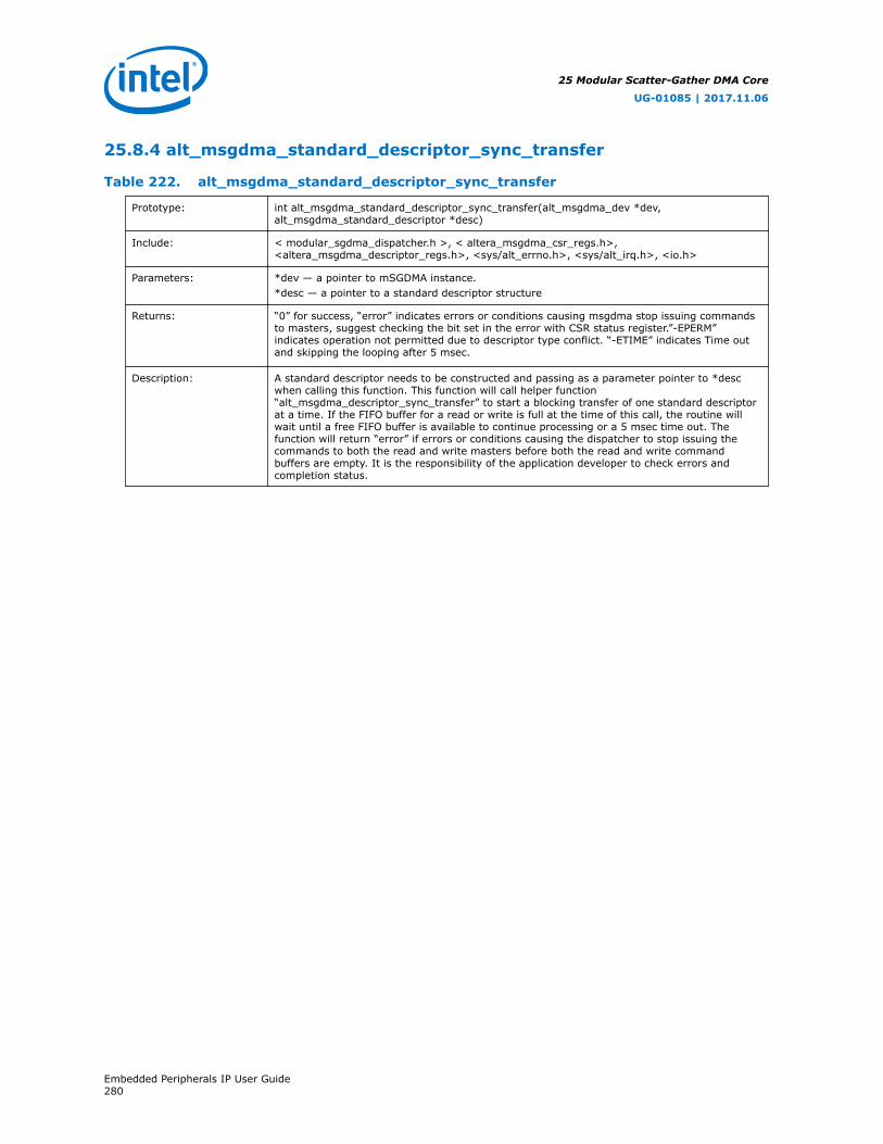
25.8.4 alt_msgdma_standard_descriptor_sync_transfer
Table 222. alt_msgdma_standard_descriptor_sync_transfer
Prototype: int alt_msgdma_standard_descriptor_sync_transfer(alt_msgdma_dev *dev,alt_msgdma_standard_descriptor *desc)
Include: < modular_sgdma_dispatcher.h >, < altera_msgdma_csr_regs.h>,<altera_msgdma_descriptor_regs.h>, <sys/alt_errno.h>, <sys/alt_irq.h>, <io.h>
Parameters: *dev — a pointer to mSGDMA instance.*desc — a pointer to a standard descriptor structure
Returns: “0” for success, “error” indicates errors or conditions causing msgdma stop issuing commandsto masters, suggest checking the bit set in the error with CSR status register.”-EPERM”indicates operation not permitted due to descriptor type conflict. “-ETIME” indicates Time outand skipping the looping after 5 msec.
Description: A standard descriptor needs to be constructed and passing as a parameter pointer to *descwhen calling this function. This function will call helper function“alt_msgdma_descriptor_sync_transfer” to start a blocking transfer of one standard descriptorat a time. If the FIFO buffer for a read or write is full at the time of this call, the routine willwait until a free FIFO buffer is available to continue processing or a 5 msec time out. Thefunction will return “error” if errors or conditions causing the dispatcher to stop issuing thecommands to both the read and write masters before both the read and write commandbuffers are empty. It is the responsibility of the application developer to check errors andcompletion status.
25 Modular Scatter-Gather DMA Core
UG-01085 | 2017.11.06
Embedded Peripherals IP User Guide280
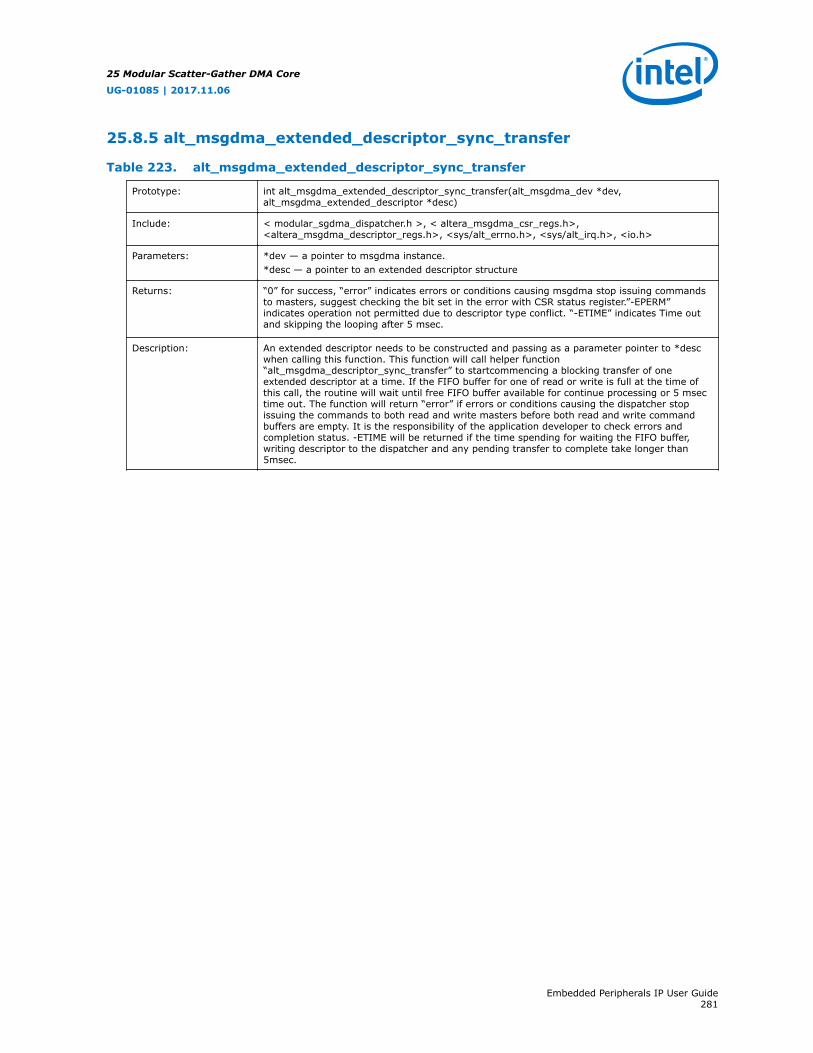
25.8.5 alt_msgdma_extended_descriptor_sync_transfer
Table 223. alt_msgdma_extended_descriptor_sync_transfer
Prototype: int alt_msgdma_extended_descriptor_sync_transfer(alt_msgdma_dev *dev,alt_msgdma_extended_descriptor *desc)
Include: < modular_sgdma_dispatcher.h >, < altera_msgdma_csr_regs.h>,<altera_msgdma_descriptor_regs.h>, <sys/alt_errno.h>, <sys/alt_irq.h>, <io.h>
Parameters: *dev — a pointer to msgdma instance.*desc — a pointer to an extended descriptor structure
Returns: “0” for success, “error” indicates errors or conditions causing msgdma stop issuing commandsto masters, suggest checking the bit set in the error with CSR status register.”-EPERM”indicates operation not permitted due to descriptor type conflict. “-ETIME” indicates Time outand skipping the looping after 5 msec.
Description: An extended descriptor needs to be constructed and passing as a parameter pointer to *descwhen calling this function. This function will call helper function“alt_msgdma_descriptor_sync_transfer” to startcommencing a blocking transfer of oneextended descriptor at a time. If the FIFO buffer for one of read or write is full at the time ofthis call, the routine will wait until free FIFO buffer available for continue processing or 5 msectime out. The function will return “error” if errors or conditions causing the dispatcher stopissuing the commands to both read and write masters before both read and write commandbuffers are empty. It is the responsibility of the application developer to check errors andcompletion status. -ETIME will be returned if the time spending for waiting the FIFO buffer,writing descriptor to the dispatcher and any pending transfer to complete take longer than5msec.
25 Modular Scatter-Gather DMA Core
UG-01085 | 2017.11.06
Embedded Peripherals IP User Guide281
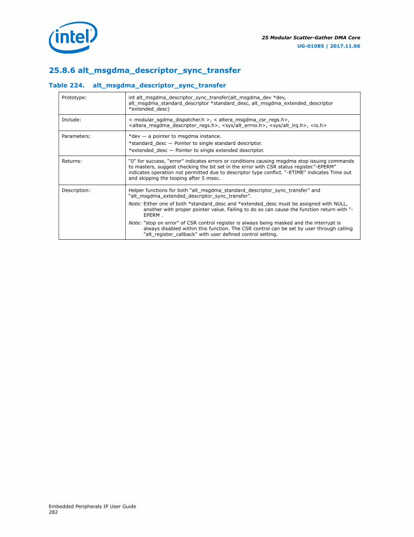
25.8.6 alt_msgdma_descriptor_sync_transfer
Table 224. alt_msgdma_descriptor_sync_transfer
Prototype: int alt_msgdma_descriptor_sync_transfer(alt_msgdma_dev *dev,alt_msgdma_standard_descriptor *standard_desc, alt_msgdma_extended_descriptor*extended_desc)
Include: < modular_sgdma_dispatcher.h >, < altera_msgdma_csr_regs.h>,<altera_msgdma_descriptor_regs.h>, <sys/alt_errno.h>, <sys/alt_irq.h>, <io.h>
Parameters: *dev — a pointer to msgdma instance.*standard_desc — Pointer to single standard descriptor.*extended_desc — Pointer to single extended descriptor.
Returns: “0” for success, “error” indicates errors or conditions causing msgdma stop issuing commandsto masters, suggest checking the bit set in the error with CSR status register.”-EPERM”indicates operation not permitted due to descriptor type conflict. “-ETIME” indicates Time outand skipping the looping after 5 msec.
Description: Helper functions for both “alt_msgdma_standard_descriptor_sync_transfer” and“alt_msgdma_extended_descriptor_sync_transfer”.Note: Either one of both *standard_desc and *extended_desc must be assigned with NULL,
another with proper pointer value. Failing to do so can cause the function return with "-EPERM .
Note: "stop on error" of CSR control register is always being masked and the interrupt isalways disabled within this function. The CSR control can be set by user through calling"alt_register_callback" with user defined control setting.
25 Modular Scatter-Gather DMA Core
UG-01085 | 2017.11.06
Embedded Peripherals IP User Guide282
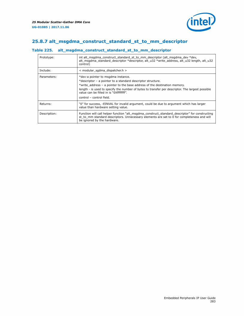
25.8.7 alt_msgdma_construct_standard_st_to_mm_descriptor
Table 225. alt_msgdma_construct_standard_st_to_mm_descriptor
Prototype: int alt_msgdma_construct_standard_st_to_mm_descriptor (alt_msgdma_dev *dev,alt_msgdma_standard_descriptor *descriptor, alt_u32 *write_address, alt_u32 length, alt_u32control)
Include: < modular_sgdma_dispatcher.h >
Parameters: *dev-a pointer to msgdma instance.*descriptor – a pointer to a standard descriptor structure.*write_address – a pointer to the base address of the destination memory.length - is used to specify the number of bytes to transfer per descriptor. The largest possiblevalue can be filled in is “0Xffffffff”.
control – control field.
Returns: “0” for success, -EINVAL for invalid argument, could be due to argument which has largervalue than hardware setting value.
Description: Function will call helper function “alt_msgdma_construct_standard_descriptor” for constructingst_to_mm standard descriptors. Unnecessary elements are set to 0 for completeness and willbe ignored by the hardware.
25 Modular Scatter-Gather DMA Core
UG-01085 | 2017.11.06
Embedded Peripherals IP User Guide283

25.8.8 alt_msgdma_construct_standard_mm_to_st_descriptor
Table 226. alt_msgdma_construct_standard_mm_to_st_descriptor
Prototype: int alt_msgdma_construct_standard_mm_to_st_descriptor (alt_msgdma_dev *dev,alt_msgdma_standard_descriptor *descriptor, alt_u32 *read_address, alt_u32 length, alt_u32control)
Include: < modular_sgdma_dispatcher.h >
Parameters: *dev-a pointer to msgdma instance.*descriptor – a pointer to a standard descriptor structure.*read_address – a pointer to the base address of the source memory.length – is used to specify the number of bytes to transfer per descriptor. The largest possiblevalue can be filled in is “0Xffffffff”.control – control field.
Returns: “0” for success, -EINVAL for invalid argument, could be due to argument which has largervalue than hardware setting value.
Description: Function will call helper function “alt_msgdma_construct_standard_descriptor” for constructingmm_to_st standard descriptors. Unnecessary elements are set to 0 for completeness and willbe ignored by the hardware.
25 Modular Scatter-Gather DMA Core
UG-01085 | 2017.11.06
Embedded Peripherals IP User Guide284
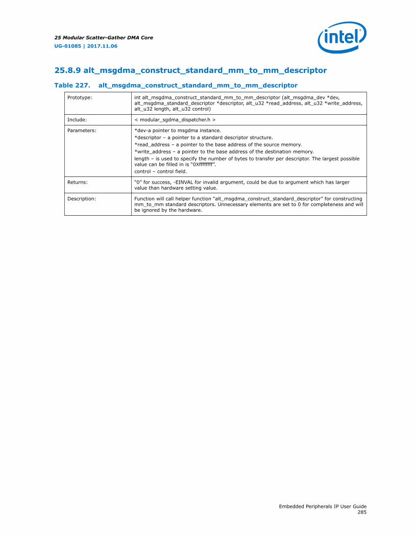
25.8.9 alt_msgdma_construct_standard_mm_to_mm_descriptor
Table 227. alt_msgdma_construct_standard_mm_to_mm_descriptor
Prototype: int alt_msgdma_construct_standard_mm_to_mm_descriptor (alt_msgdma_dev *dev,alt_msgdma_standard_descriptor *descriptor, alt_u32 *read_address, alt_u32 *write_address,alt_u32 length, alt_u32 control)
Include: < modular_sgdma_dispatcher.h >
Parameters: *dev-a pointer to msgdma instance.*descriptor – a pointer to a standard descriptor structure.*read_address – a pointer to the base address of the source memory.*write_address – a pointer to the base address of the destination memory.length – is used to specify the number of bytes to transfer per descriptor. The largest possiblevalue can be filled in is “0Xffffffff”.control – control field.
Returns: “0” for success, -EINVAL for invalid argument, could be due to argument which has largervalue than hardware setting value.
Description: Function will call helper function “alt_msgdma_construct_standard_descriptor” for constructingmm_to_mm standard descriptors. Unnecessary elements are set to 0 for completeness and willbe ignored by the hardware.
25 Modular Scatter-Gather DMA Core
UG-01085 | 2017.11.06
Embedded Peripherals IP User Guide285
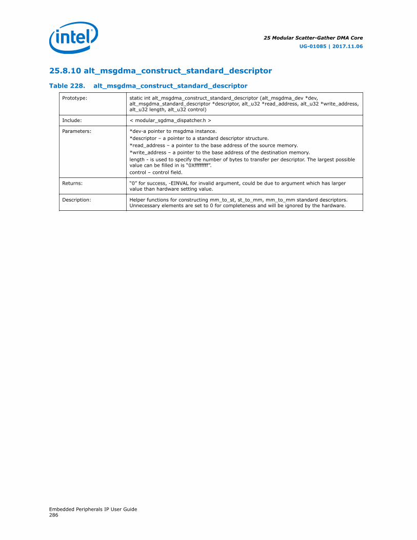
25.8.10 alt_msgdma_construct_standard_descriptor
Table 228. alt_msgdma_construct_standard_descriptor
Prototype: static int alt_msgdma_construct_standard_descriptor (alt_msgdma_dev *dev,alt_msgdma_standard_descriptor *descriptor, alt_u32 *read_address, alt_u32 *write_address,alt_u32 length, alt_u32 control)
Include: < modular_sgdma_dispatcher.h >
Parameters: *dev-a pointer to msgdma instance.*descriptor – a pointer to a standard descriptor structure.*read_address – a pointer to the base address of the source memory.*write_address – a pointer to the base address of the destination memory.length - is used to specify the number of bytes to transfer per descriptor. The largest possiblevalue can be filled in is “0Xffffffff”.control – control field.
Returns: “0” for success, -EINVAL for invalid argument, could be due to argument which has largervalue than hardware setting value.
Description: Helper functions for constructing mm_to_st, st_to_mm, mm_to_mm standard descriptors.Unnecessary elements are set to 0 for completeness and will be ignored by the hardware.
25 Modular Scatter-Gather DMA Core
UG-01085 | 2017.11.06
Embedded Peripherals IP User Guide286
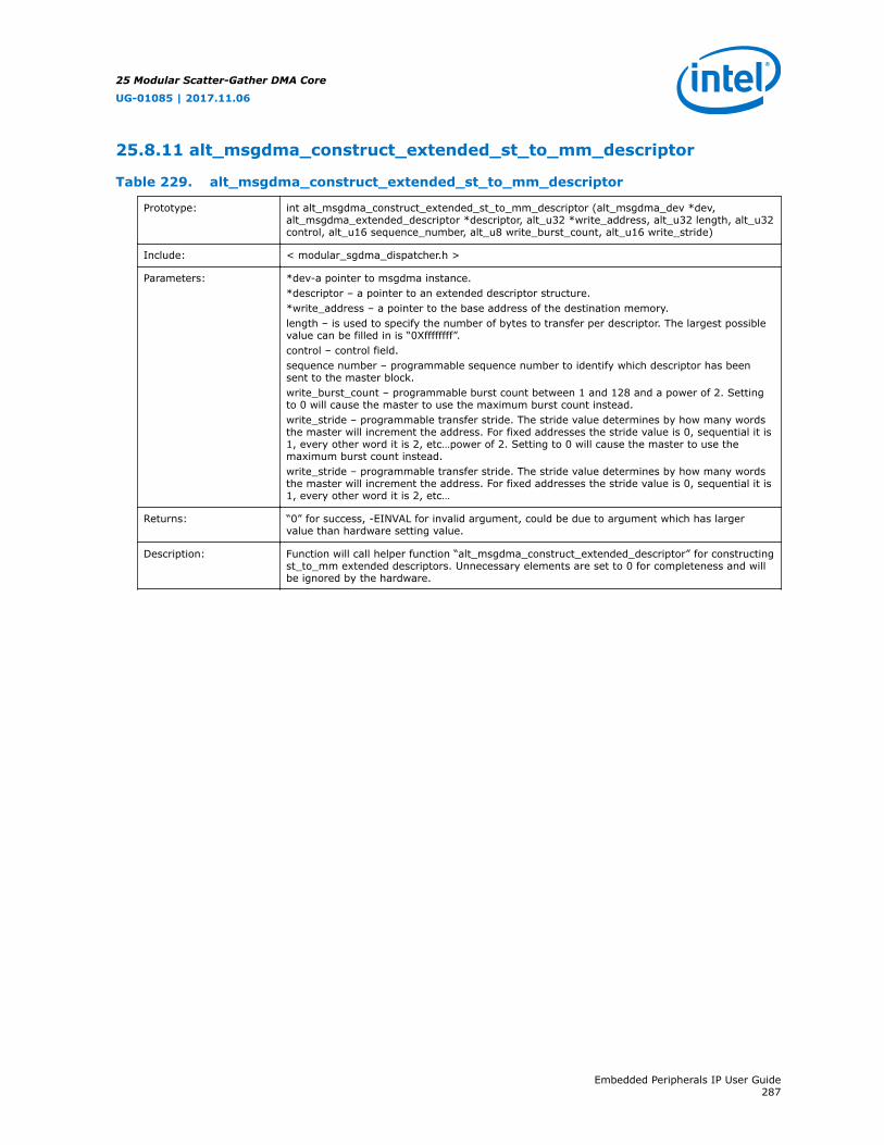
25.8.11 alt_msgdma_construct_extended_st_to_mm_descriptor
Table 229. alt_msgdma_construct_extended_st_to_mm_descriptor
Prototype: int alt_msgdma_construct_extended_st_to_mm_descriptor (alt_msgdma_dev *dev,alt_msgdma_extended_descriptor *descriptor, alt_u32 *write_address, alt_u32 length, alt_u32control, alt_u16 sequence_number, alt_u8 write_burst_count, alt_u16 write_stride)
Include: < modular_sgdma_dispatcher.h >
Parameters: *dev-a pointer to msgdma instance.*descriptor – a pointer to an extended descriptor structure.*write_address – a pointer to the base address of the destination memory.length – is used to specify the number of bytes to transfer per descriptor. The largest possiblevalue can be filled in is “0Xffffffff”.control – control field.sequence number – programmable sequence number to identify which descriptor has beensent to the master block.write_burst_count – programmable burst count between 1 and 128 and a power of 2. Settingto 0 will cause the master to use the maximum burst count instead.write_stride – programmable transfer stride. The stride value determines by how many wordsthe master will increment the address. For fixed addresses the stride value is 0, sequential it is1, every other word it is 2, etc…power of 2. Setting to 0 will cause the master to use themaximum burst count instead.write_stride – programmable transfer stride. The stride value determines by how many wordsthe master will increment the address. For fixed addresses the stride value is 0, sequential it is1, every other word it is 2, etc…
Returns: “0” for success, -EINVAL for invalid argument, could be due to argument which has largervalue than hardware setting value.
Description: Function will call helper function “alt_msgdma_construct_extended_descriptor” for constructingst_to_mm extended descriptors. Unnecessary elements are set to 0 for completeness and willbe ignored by the hardware.
25 Modular Scatter-Gather DMA Core
UG-01085 | 2017.11.06
Embedded Peripherals IP User Guide287

25.8.12 alt_msgdma_construct_extended_mm_to_st_descriptor
Table 230. alt_msgdma_construct_extended_mm_to_st_descriptor
Prototype: int alt_msgdma_construct_extended_mm_to_st_descriptor (alt_msgdma_dev *dev,alt_msgdma_extended_descriptor *descriptor, alt_u32 *read_address, alt_u32 length, alt_u32control, alt_u16 sequence_number, alt_u8 read_burst_count, alt_u16 read_stride)
Include: < modular_sgdma_dispatcher.h >
Parameters: *dev-a pointer to msgdma instance.*descriptor – a pointer to an extended descriptor structure.*read_address – a pointer to the base address of the source memory.length – is used to specify the number of bytes to transfer per descriptor. The largest possiblevalue can be filled in is “0Xffffffff”.control – control field.sequence_number – programmable sequence number to identify which descriptor has beensent to the master block.read_burst_count – programmable burst count between 1 and 128 and a power of 2. Settingto 0 will cause the master to use the maximum burst count instead.read_stride – programmable transfer stride. The stride value determines by how many wordsthe master will increment the address. For fixed addresses the stride value is 0, sequential it is1, every other word it is 2, etc…
Returns: “0” for success, -EINVAL for invalid argument, could be due to argument which has largervalue than hardware setting value.
Description: Function call helper function “alt_msgdma_construct_extended_descriptor” for constructingmm_to_st extended descriptors. Unnecessary elements are set to 0 for completeness and willbe ignored by the hardware.
25 Modular Scatter-Gather DMA Core
UG-01085 | 2017.11.06
Embedded Peripherals IP User Guide288
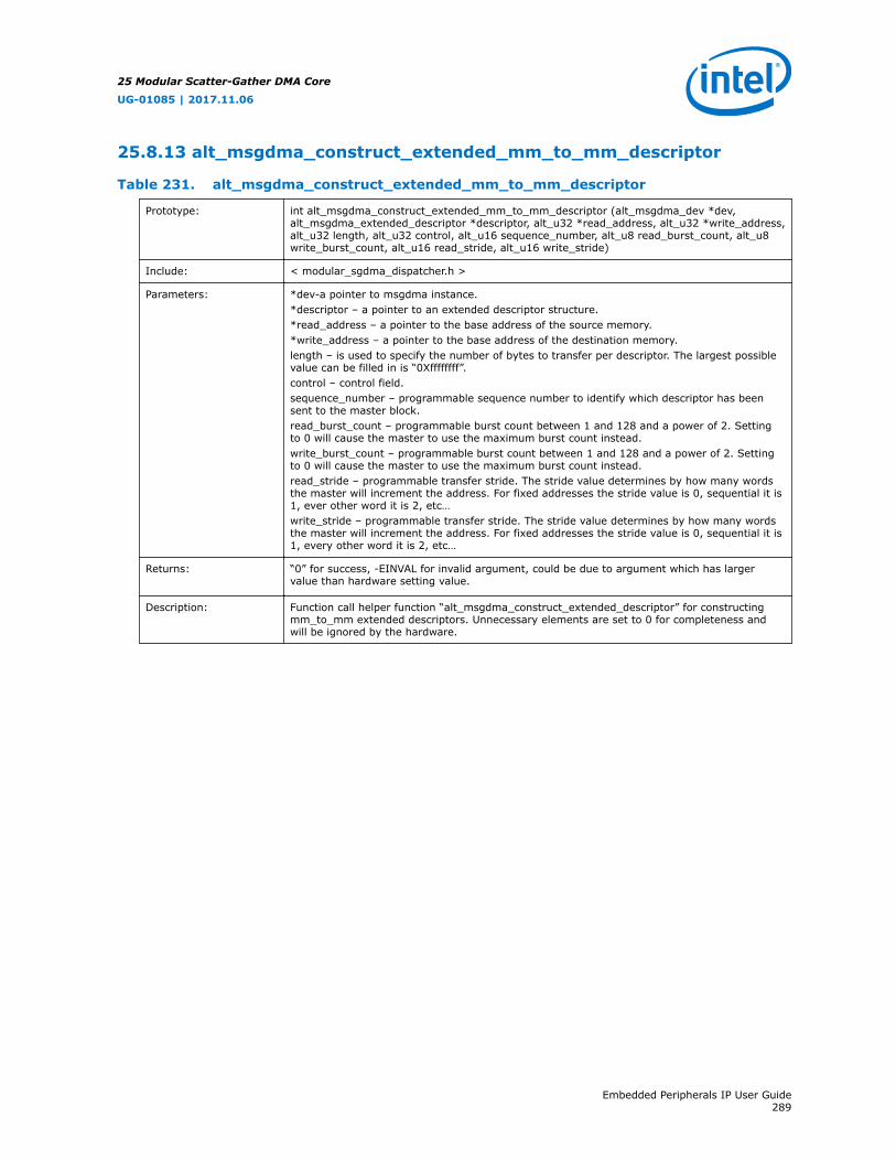
25.8.13 alt_msgdma_construct_extended_mm_to_mm_descriptor
Table 231. alt_msgdma_construct_extended_mm_to_mm_descriptor
Prototype: int alt_msgdma_construct_extended_mm_to_mm_descriptor (alt_msgdma_dev *dev,alt_msgdma_extended_descriptor *descriptor, alt_u32 *read_address, alt_u32 *write_address,alt_u32 length, alt_u32 control, alt_u16 sequence_number, alt_u8 read_burst_count, alt_u8write_burst_count, alt_u16 read_stride, alt_u16 write_stride)
Include: < modular_sgdma_dispatcher.h >
Parameters: *dev-a pointer to msgdma instance.*descriptor – a pointer to an extended descriptor structure.*read_address – a pointer to the base address of the source memory.*write_address – a pointer to the base address of the destination memory.length – is used to specify the number of bytes to transfer per descriptor. The largest possiblevalue can be filled in is “0Xffffffff”.control – control field.sequence_number – programmable sequence number to identify which descriptor has beensent to the master block.read_burst_count – programmable burst count between 1 and 128 and a power of 2. Settingto 0 will cause the master to use the maximum burst count instead.write_burst_count – programmable burst count between 1 and 128 and a power of 2. Settingto 0 will cause the master to use the maximum burst count instead.read_stride – programmable transfer stride. The stride value determines by how many wordsthe master will increment the address. For fixed addresses the stride value is 0, sequential it is1, ever other word it is 2, etc…write_stride – programmable transfer stride. The stride value determines by how many wordsthe master will increment the address. For fixed addresses the stride value is 0, sequential it is1, every other word it is 2, etc…
Returns: “0” for success, -EINVAL for invalid argument, could be due to argument which has largervalue than hardware setting value.
Description: Function call helper function “alt_msgdma_construct_extended_descriptor” for constructingmm_to_mm extended descriptors. Unnecessary elements are set to 0 for completeness andwill be ignored by the hardware.
25 Modular Scatter-Gather DMA Core
UG-01085 | 2017.11.06
Embedded Peripherals IP User Guide289

25.8.14 alt_msgdma_construct_extended_descriptor
Table 232. alt_msgdma_construct_extended_descriptor
Prototype: static int alt_msgdma_construct_descriptor (alt_msgdma_dev *dev,alt_msgdma_extended_descriptor *descriptor, alt_u32 *read_address, alt_u32 *write_address,alt_u32 length, alt_u32 control, alt_u16 sequence_number, alt_u8 read_burst_count, alt_u8write_burst_count,alt_u16 read_stride, alt_u16 write_stride)
Include: < modular_sgdma_dispatcher.h >
Parameters: *dev-a pointer to msgdma instance.*descriptor – a pointer to an extended descriptor structure.*read_address – a pointer to the base address of the source memory.*write_address – a pointer to the base address of the destination memory.length – is used to specify the number of bytes to transfer per descriptor. The largest possiblevalue can be filled in is “0Xffffffff”.control – control field.sequence_number – programmable sequence number to identify which descriptor has beensent to the master block.read_burst_count – programmable burst count between 1 and 128 and a power of 2. Settingto 0 will cause the master to use the maximum burst count instead.write_burst_count – programmable burst count between 1 and 128 and a power of 2. Settingto 0 will cause the master to use the maximum burst count instead.read_stride – programmable transfer stride. The stride value determines by how many wordsthe master will increment the address. For fixed addresses the stride value is 0, sequential it is1, ever other word it is 2, etc…write_stride – programmable transfer stride. The stride value determines by how many wordsthe master will increment the address. For fixed addresses the stride value is 0, sequential it is1, every other word it is 2, etc…
Returns: “0” for success, -EINVAL for invalid argument, could be due to argument which has largervalue than hardware setting value.
Description: Helper functions for constructing mm_to_st, st_to_mm, mm_to_mm extended descriptors.Unnecessary elements are set to 0 for completeness and will be ignored by the hardware.
25 Modular Scatter-Gather DMA Core
UG-01085 | 2017.11.06
Embedded Peripherals IP User Guide290

25.8.15 alt_msgdma_register_callback
Table 233. alt_msgdma_register_callback
Prototype: void alt_msgdma_register_callback(alt_msgdma_dev *dev, alt_msgdma_callback callback,alt_u32 control, void *context)
Include: < modular_sgdma_dispatcher.h >
Parameters: *dev — a pointer to msgdma instance.callback — Pointer to callback routine to execute at interrupt levelcontrol — Setting control register and OR with other control bits in the non_blocking andblocking transfer function.*context — pointer to user define context
Returns: N/A
Description: Associate a user-specific routine with the mSGDMA interrupt handler. If a callback is registered,all non-blocking mSGDMA transfers will enable interrupts that will cause the callback to beexecuted. The callback runs as part of the interrupt service routine, and great care must betaken to follow the guidelines for acceptable interrupt service routine behavior as described inthe Nios II Software Developer's Handbook. However, user can change some of the CSR controlsetting in blocking transfer by calling this function.
25 Modular Scatter-Gather DMA Core
UG-01085 | 2017.11.06
Embedded Peripherals IP User Guide291

25.8.16 alt_msgdma_open
Table 234. alt_msgdma_open
Prototype: alt_msgdma_dev* alt_msgdma_open (const char* name)
Include: < modular_sgdma_dispatcher.h >
Parameters: *name — Character pointer to name of msgdma peripheral as registered with the HAL. Forexample, an mSGDMA in Platform Designer would be opened by asking for“MSGDMA_0_DISPATCHER_INTERNAL".
Returns: Pointer to msgdma device instance struct, or null if the device.* could not be opened.
Description: Retrieves a pointer to the mSGDMA instance.
25 Modular Scatter-Gather DMA Core
UG-01085 | 2017.11.06
Embedded Peripherals IP User Guide292

25.8.17 alt_msgdma_write_standard_descriptor
Table 235. alt_msgdma_write_standard_descriptor
Prototype: int alt_msgdma_write_standard_descriptor (alt_u32 csr_base, alt_u32 descriptor_base,alt_msgdma_standard_descriptor *descriptor)
Include: < modular_sgdma_dispatcher.h >, <altera_msgdma_descriptor_regs.h>
Parameters: csr_base – base address of the dispatcher CSR slave port.descriptor_base – base address of the dispatcher descriptor slave port.*descriptor – a pointer to a standard descriptor structure.
Returns: Returns 0 upon success. Other return codes are defined in "alt_errno.h".
Description: Sends a fully formed standard descriptor to the dispatcher module. If the dispatcher descriptorbuffer is full, “-ENOSPC” is returned. This function is not reentrant since it must completewriting the entire descriptor to the dispatcher module and cannot be pre-empted.
25 Modular Scatter-Gather DMA Core
UG-01085 | 2017.11.06
Embedded Peripherals IP User Guide293
25.8.18 alt_msgdma_write_extended_descriptor
Table 236. alt_msgdma_write_extended_descriptor
Prototype: int alt_msgdma_write_extended_descriptor (alt_u32 csr_base, alt_u32 descriptor_base,alt_msgdma_extended_descriptor *descriptor)
Include: < modular_sgdma_dispatcher.h >, <altera_msgdma_descriptor_regs.h>
Parameters: csr_base – base address of the dispatcher CSR slave port.descriptor_base – base address of the dispatcher descriptor slave port.*descriptor – a pointer to an extended descriptor structure.
Returns: Returns 0 upon success. Other return codes are defined in "alt_errno.h".
Description: Sends a fully formed extended descriptor to the dispatcher module. If the dispatcher descriptorbuffer is full an error is returned. This function is not reentrant since it must complete writingthe entire descriptor to the dispatcher module and cannot be pre-empted.
25 Modular Scatter-Gather DMA Core
UG-01085 | 2017.11.06
Embedded Peripherals IP User Guide294
25.8.19 alt_avalon_msgdma_init
Table 237. alt_avalon_msgdma_init
Prototype: void alt_msgdma_init (alt_msgdma_dev *dev, alt_u32 ic_id, alt_u32 irq)
Include: < modular_sgdma_dispatcher.h >, <altera_msgdma_descriptor_regs.h>,<altera_msgdma_csr_regs.h>
Parameters: *dev – a pointer to mSGDMA instance.ic_id – id of irq interrupt controllerirq – irq number that belonged to mSGDMA instance
Returns: N/A
Description: Initializes the mSGDMA controller. This routine is called from theALTERA_AVALON_MSGDMA_INIT macro and is called automatically by "alt_sys_init.c".
25.8.20 alt_msgdma_irq
Table 238. alt_msgdma_irq
Prototype: void alt_msgdma_irq(void *context)
Include: < modular_sgdma_dispatcher.h >, <sys/alt_irq.h>, <altera_msgdma_csr_regs.h>
Parameters: *context – a pointer to mSGDMA instance.
Returns: N/A
Description: Interrupt handler for mSGDMA. This function will call the user defined interrupt handler if userregisters their own interrupt handler with calling “alt_register_callback”.
25 Modular Scatter-Gather DMA Core
UG-01085 | 2017.11.06
Embedded Peripherals IP User Guide295
25.9 Document Revision History
Table 239. Modular Scatter-Gather DMA Core Revision History
Date Version Changes
May 2017 2017.05.08 Status Register on page 261 : Bit 9 description updated
May 2016 2016.05.03 Updated tables:• Component Parameters
December 2015 2015.12.16 Added "alt_msgdma_irq" section.
November 2015 2015.11.06 Updated sections:• Response Port• Component ParametersSections added:• Programming Model
— Stop DMA Operation— Stop Descriptor Operation— Recovery from Stopped on Error and Stopped on Early Termination
• Modular Scatter-Gather DMA Prefetcher Core• Driver ImplementationSection removed:• Unsupported Feature
July 2014 2014.07.24 Initial release
25 Modular Scatter-Gather DMA Core
UG-01085 | 2017.11.06
Embedded Peripherals IP User Guide296
26 Scatter-Gather DMA Controller CoreIntel recommends to use Modular Scatter-Gather DMA Core for your new designs.
26.1 Core Overview
The Scatter-Gather Direct Memory Access (SG-DMA) controller core implements high-speed data transfer between two components. You can use the SG-DMA controllercore to transfer data from:
• Memory to memory
• Data stream to memory
• Memory to data stream
The SG-DMA controller core transfers and merges non-contiguous memory to acontinuous address space, and vice versa. The core reads a series of descriptors thatspecify the data to be transferred.
For applications requiring more than one DMA channel, multiple instantiations of thecore can provide the required throughput. Each SG-DMA controller has its own seriesof descriptors specifying the data transfers. A single software module controls all ofthe DMA channels.
For the Nios II processor, device drivers are provided in the Hardware AbstractionLayer (HAL) system library, allowing software to access the core using the provideddriver.
26.1.1 Example Systems
The block diagram below shows a SG-DMA controller core for the DMA subsystem of aprinted circuit board. The SG-DMA core in the FPGA reads streaming data from aninternal streaming component and writes data to an external memory. A Nios IIprocessor provides overall system control.
UG-01085 | 2017.11.06
Intel Corporation. All rights reserved. Intel, the Intel logo, Altera, Arria, Cyclone, Enpirion, MAX, Nios, Quartusand Stratix words and logos are trademarks of Intel Corporation or its subsidiaries in the U.S. and/or othercountries. Intel warrants performance of its FPGA and semiconductor products to current specifications inaccordance with Intel's standard warranty, but reserves the right to make changes to any products and servicesat any time without notice. Intel assumes no responsibility or liability arising out of the application or use of anyinformation, product, or service described herein except as expressly agreed to in writing by Intel. Intelcustomers are advised to obtain the latest version of device specifications before relying on any publishedinformation and before placing orders for products or services.*Other names and brands may be claimed as the property of others.
ISO9001:2008Registered

Figure 75. SG-DMA Controller Core with Streaming Peripheral and External Memory
S
Rd
SNKM
Rd
M M
Wr
M
Wr
M
S
SNK
M
Intel FPGA
SOPC Builder System
Scatter Gather DMA Controller Core
Control andStatus
Registers
DescriptorProcessor
Block
DMA WriteBlock
MemoryController
MemoryNios II
ProcessorStreaming
ComponentDescriptorTable
DDR2SDRAM
System Interconnect Fabric
Avalon-MM Master Port
Avalon-MM Slave Port
Avalon-ST Sink Port
The figure below shows a different use of the SG-DMA controller core, where the coretransfers data between an internal and external memory. The host processor andmemory are connected to a system bus, typically either a PCI Express or SerialRapidIO™.
Figure 76. SG-DMA Controller Core with Internal and External Memory
Process orBus
S
Host Process or
InternalMemo ry
M M
Sys tem Interconnec t Fa bric
S
Rd
M
Des criptorProces sor
Block
Rd
M
DMA Read/WriteBlock
Wr
M
Wr
M
Con trol &
Stat us Reg iste rs
Scatter Gather DMA Controlle r Core
Avalon-MM Bridge
M S
IOB
Main Memo ry
Desc riptorTable
S Avalon-MM Slave Por t
M Avalon-MM Master Port
IOB IO Breakout
Intel FPGA
Platform Designer
26 Scatter-Gather DMA Controller Core
UG-01085 | 2017.11.06
Embedded Peripherals IP User Guide298
26.1.2 Comparison of SG-DMA Controller Core and DMA Controller Core
The SG-DMA controller core provides a significant performance enhancement over thepreviously available DMA controller core, which could only queue one transfer at atime. Using the DMA Controller core, a CPU had to wait for the transfer to completebefore writing a new descriptor to the DMA slave port. Transfers to non-contiguousmemory could not be linked; consequently, the CPU overhead was substantial forsmall transfers, degrading overall system performance. In contrast, the SG-DMAcontroller core reads a series of descriptors from memory that describe the requiredtransactions and performs all of the transfers without additional intervention from theCPU.
26.2 Resource Usage and Performance
Resource utilization for the core is 600–1400 logic elements, depending upon thewidth of the datapath, the parameterization of the core, the device family, and thetype of data transfer. The table below provides the estimated resource usage for a SG-DMA controller core used for memory to memory transfer. The core is configurable andthe resource utilization varies with the configuration specified.
Table 240. SG-DMA Estimated Resource Usage
Datapath Cyclone II Stratix> (LEs)
Stratix II(ALUTs)
8-bit datapath 850 650 600
32-bit datapath 1100 850 700
64-bit datapath 1250 1250 800
The core operating frequency varies with the device and the size of the datapath. Thetable below provides an example of expected performance for SG-DMA coresinstantiated in several different device families.
Table 241. SG-DMA Peak Performance
Device Datapath fMAX Throughput
Cyclone II 64 bits 150 MHz 9.6 Gbps
Cyclone III 64 bits 160 MHz 10.2 Gbps
Stratix II/Stratix II GX 64 bits 250 MHz 16.0 Gbps
Stratix III 64 bits 300 MHz 19.2 Gbps
26.3 Functional Description
The SG-DMA controller core comprises three major blocks: descriptor processor, DMAread, and DMA write. These blocks are combined to create three differentconfigurations:
26 Scatter-Gather DMA Controller Core
UG-01085 | 2017.11.06
Embedded Peripherals IP User Guide299

• Memory to memory
• Memory to stream
• Stream to memory
The type of devices you are transferring data to and from determines theconfiguration to implement. Examples of memory-mapped devices are PCI, PCIeand most memory devices. The Triple Speed Ethernet MAC, DSP IP core and manyvideo IPs are examples of streaming devices. A recompilation is necessary eachtime you change the configuration of the SG-DMA controller core.
26.3.1 Functional Blocks and Configurations
The following sections describe each functional block and configuration.
Descriptor Processor
The descriptor processor reads descriptors from the descriptor list via its AvalonMemory-Mapped (MM) read master port and pushes commands into the commandFIFOs of the DMA read and write blocks. Each command includes the following fieldsto specify a transfer:
• Source address
• Destination address
• Number of bytes to transfer
• Increment read address after each transfer
• Increment write address after each transfer
• Generate start of packet (SOP) and end of packet (EOP)
After each command is processed by the DMA read or write block, a status tokencontaining information about the transfer such as the number of bytes actuallywritten is returned to the descriptor processor, where it is written to the respectivefields in the descriptor.
DMA Read Block
The DMA read block is used in memory-to-memory and memory-to-streamconfigurations. The block performs the following operations:
• Reads commands from the input command FIFO.
• Reads a block of memory via the Avalon-MM read master port for each command.
• Pushes data into the data FIFO.
If burst transfer is enabled, an internal read FIFO with a depth of twice themaximum read burst size is instantiated. The DMA read block initiates burst readsonly when the read FIFO has sufficient space to buffer the complete burst.
DMA Write Block
The DMA write block is used in memory-to-memory and stream-to-memoryconfigurations. The block reads commands from its input command FIFO. For eachcommand, the DMA write block reads data from its Avalon-ST sink port and writes it tothe Avalon-MM master port.
26 Scatter-Gather DMA Controller Core
UG-01085 | 2017.11.06
Embedded Peripherals IP User Guide300

If burst transfer is enabled, an internal write FIFO with a depth of twice the maximumwrite burst size is instantiated. Each burst write transfers a fixed amount of dataequals to the write burst size, except for the last burst. In the last burst, theremaining data is transferred even if the amount of data is less than the write burstsize.
Memory-to-Memory Configuration
Memory-to-memory configurations include all three blocks: descriptor processor, DMAread, and DMA write. An internal FIFO is also included to provide buffering and flowcontrol for data transferred between the DMA read and write blocks.
The example below illustrates one possible memory-to-memory configuration with aninternal Nios II processor and descriptor list.
Figure 77. Example of Memory-to-Memory Configuration
M
S
Intel FPGA
S MM M M
Platform Designer System
Scatter Gather DMA Controller Core
Control &Status
Registers
DescriptorProcessor Block
DMA Write Block
SNK
SRC
DMA Read Block
System Interconnect Fabric
MemoryController
MemoryNios II
ProcessorDescriptorTable
DDR2SDRAM
Avalon-MM Master Port
Avalon-MM Slave Port
Avalon-ST Source Port
Avalon-ST Sink Port
SRC
SNK
commandstatusstatuscommand
DataFIFO
Wr Rd
Memory-to-Stream Configuration
Memory-to-stream configurations include the descriptor processor and DMA readblocks.
In this example, the Nios II processor and descriptor table are in the FPGA. Data froman external DDR2 SDRAM is read by the SG-DMA controller and written to an on-chipstreaming peripheral.
26 Scatter-Gather DMA Controller Core
UG-01085 | 2017.11.06
Embedded Peripherals IP User Guide301
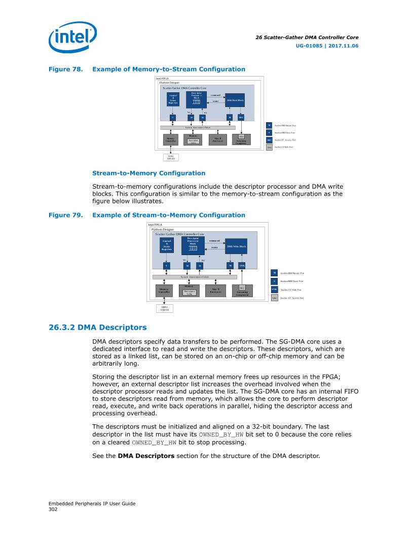
Figure 78. Example of Memory-to-Stream Configuration
SNK
M Avalon-MM Master Port
S Avalon-MM S lave P ort
Avalon-ST Source Port
Avalon-ST Sink Port
Sc atter Gat her DMA Controller Core
Rd
S M
Wr
M M
command
s tatus
SRC
Contro l &
S tatus Regis ters
Nios IIProcess or
DDR2SDR AM
MemoryController
Memory
DescriptorTab le
DMA Rea d Block
Descr iptorProcesso r
Block
SRCStreamingComponent
SNK
System Inter connec t Fab ric
Intel FPGA
Platform Designer
Stream-to-Memory Configuration
Stream-to-memory configurations include the descriptor processor and DMA writeblocks. This configuration is similar to the memory-to-stream configuration as thefigure below illustrates.
Figure 79. Example of Stream-to-Memory Configuration
SRC
SRC
M Avalon-MM Master Port
S Avalon-MM S lave P ort
Avalon-ST So urce Port
Avalon-ST S ink Port
Sca tte r Ga ther DMA Controlle r Core
Rd
S M
Wr
M M
comma nd
st atus
SN K
Con trol &
Sta tus Regis ters
Nios IIProces s or
DDR2SDRAM
Memo ryCon troller
System Interconne ct Fabric
Memo ry
DescriptorTable
Des criptorProc es s or
Block
SNK
DMA Write Block
StreamingCompon ent
SR C
Intel FPGA
Platform Designer
26.3.2 DMA Descriptors
DMA descriptors specify data transfers to be performed. The SG-DMA core uses adedicated interface to read and write the descriptors. These descriptors, which arestored as a linked list, can be stored on an on-chip or off-chip memory and can bearbitrarily long.
Storing the descriptor list in an external memory frees up resources in the FPGA;however, an external descriptor list increases the overhead involved when thedescriptor processor reads and updates the list. The SG-DMA core has an internal FIFOto store descriptors read from memory, which allows the core to perform descriptorread, execute, and write back operations in parallel, hiding the descriptor access andprocessing overhead.
The descriptors must be initialized and aligned on a 32-bit boundary. The lastdescriptor in the list must have its OWNED_BY_HW bit set to 0 because the core relieson a cleared OWNED_BY_HW bit to stop processing.
See the DMA Descriptors section for the structure of the DMA descriptor.
26 Scatter-Gather DMA Controller Core
UG-01085 | 2017.11.06
Embedded Peripherals IP User Guide302

Descriptor Processing
The following steps describe how the DMA descriptors are processed:
1. Software builds the descriptor linked list. See the Building and UpdatingDescriptors List section for more information on how to build and update thedescriptor linked list.
2. Software writes the address of the first descriptor to thenext_descriptor_pointer register and initiates the transfer by setting theRUN bit in the control register to 1. See the Software Programming Modelsection for more information on the registers.
On the next clock cycle following the assertion of the RUN bit, the core sets theBUSY bit in the status register to 1 to indicate that descriptor processing isexecuting.
3. The descriptor processor block reads the address of the first descriptor from thenext_descriptor_pointer register and pushes the retrieved descriptor intothe command FIFO, which feeds commands to both the DMA read and writeblocks. As soon as the first descriptor is read, the block reads the next descriptorand pushes it into the command FIFO. One descriptor is always read in advancethus maximizing throughput.
4. The core performs the data transfer.
• In memory-to-memory configurations, the DMA read block receives the sourceaddress from its command FIFO and starts reading data to fill the FIFO on itsstream port until the specified number of bytes are transferred. The DMA readblock pauses when the FIFO is full until the FIFO has enough space to acceptmore data.
The DMA write block gets the destination address from its command FIFO andstarts writing until the specified number of bytes are transferred. If the dataFIFO ever empties, the write block pauses until the FIFO has more data towrite.
• In memory-to-stream configurations, the DMA read block reads from thesource address and transfers the data to the core’s streaming port until thespecified number of bytes are transferred or the end of packet is reached. Theblock uses the end-of-packet indicator for transfers with an unknown transfersize. For data transfers without using the end-of-packet indicator, the transfersize must be a multiple of the data width. Otherwise, the block requires extralogic and may impact the system performance.
• In stream-to-memory configurations, the DMA write block reads from thecore’s streaming port and writes to the destination address. The blockcontinues reading until the specified number of bytes are transferred.
5. The descriptor processor block receives a status from the DMA read or write blockand updates the DESC_CONTROL, DESC_STATUS, andACTUAL_BYTES_TRANSFERRED fields in the descriptor. The OWNED_BY_HW bit inthe DESC_CONTROL field is cleared unless the PARK bit is set to 1.
Once the core starts processing the descriptors, software must not updatedescriptors with OWNED_BY_HW bit set to 1. It is only safe for software to update adescriptor when its OWNED_BY_HW bit is cleared.
26 Scatter-Gather DMA Controller Core
UG-01085 | 2017.11.06
Embedded Peripherals IP User Guide303

The SG-DMA core continues processing the descriptors until an error conditionoccurs and the STOP_DMA_ER bit is set to 1, or a descriptor with a clearedOWNED_BY_HW bit is encountered.
Building and Updating Descriptor List
Intel recommends the following method of building and updating the descriptor list:
1. Build the descriptor list and terminate the list with a non-hardware owneddescriptor (OWNED_BY_HW = 0). The list can be arbitrarily long.
2. Set the interrupt IE_CHAIN_COMPLETED.
3. Write the address of the first descriptor in the first list to thenext_descriptor_pointer register and set the RUN bit to 1 to initiatetransfers.
4. While the core is processing the first list, build a second list of descriptors.
5. When the SD-DMA controller core finishes processing the first list, an interrupt isgenerated. Update the next_descriptor_pointer register with the address ofthe first descriptor in the second list. Clear the RUN bit and the status register.Set the RUN bit back to 1 to resume transfers.
6. If there are new descriptors to add, always add them to the list which the core isnot processing. For example, if the core is processing the first list, add newdescriptors to the second list and so forth.
This method ensures that the descriptors are not updated when the core isprocessing them. Because the method requires a response to the interrupt, ahigh-latency interrupt may cause a problem in systems where stalling datamovement is not possible.
26.3.3 Error Conditions
The SG-DMA core has a configurable error width. Error signals are connected directlyto the Avalon-ST source or sink to which the SG-DMA core is connected.
26 Scatter-Gather DMA Controller Core
UG-01085 | 2017.11.06
Embedded Peripherals IP User Guide304

The list below describes how the error signals in the SG-DMA core are implemented inthe folowing configurations:
• Memory-to-memory configuration
No error signals are generated. The error field in the register and descriptor ishardcoded to 0.
• Memory-to-stream configuration
If you specified the usage of error bits in the core, the error bits are generated inthe Avalon-ST source interface. These error bits are hardcoded to 0 and generatedin compliance with the Avalon-ST slave interfaces.
• Stream-to-memory configuration
If you specified the usage of error bits in the core, error bits are generated in theAvalon-ST sink interface. These error bits are passed from the Avalon-ST sinkinterface and stored in the registers and descriptor.
The table below lists the error signals when the core is operating in the memory-to-stream configuration and connected to the transmit FIFO interface of the IntelFPGA Triple-Speed Ethernet IP core.
Table 242. Avalon-ST Transmit Error Types
Signal Type Description
TSE_transmit_error[0] Transmit Frame Error. Asserted to indicate that thetransmitted frame should be viewed as invalid by theEthernet MAC. The frame is then transferred onto the GMIIinterface with an error code during the frame transfer.
The table below lists the error signals when the core is operating in the stream-to-memory configuration and connected to the transmit FIFO interface of the Triple-Speed Ethernet IP Core.
Table 243. Avalon-ST Receive Error Types
Signal Type Description
TSE_receive_error[0] Receive Frame Error. This signal indicates that an error hasoccurred. It is the logical OR of receive errors 1 through 5.
TSE_receive_error[1] Invalid Length Error. Asserted when the received frame hasan invalid length as defined by the IEEE 802.3 standard.
TSE_receive_error[2] CRC Error. Asserted when the frame has been received witha CRC-32 error.
TSE_receive_error[3] Receive Frame Truncated. Asserted when the received framehas been truncated due to receive FIFO overflow.
TSE_receive_error[4] Received Frame corrupted due to PHY error. (The PHY hasasserted an error on the receive GMII interface.)
TSE_receive_error[5] Collision Error. Asserted when the frame was received with acollision.
Each streaming core has a different set of error codes. Refer to the respective userguides for the codes.
26 Scatter-Gather DMA Controller Core
UG-01085 | 2017.11.06
Embedded Peripherals IP User Guide305
26.4 Parameters
Table 244. Configurable Parameters
Parameter Legal Values Description
Transfer mode Memory To MemoryMemory To StreamStream To Memory
Configuration to use. For more information about theseconfigurations, see the Memory-to-Memory Configurationsection.
Enable bursting ondescriptor read master
On/Off If this option is on, the descriptor processor block uses Avalon-MMbursting when fetching descriptors and writing them back in memory.With 32-bit read and write ports, the descriptor processor block canfetch the 256-bit descriptor by performing 8-word burst as opposedto eight individual single-word transactions.
Allow unalignedtransfers
On/Off If this option is on, the core allows accesses to non-word-alignedaddresses. This option doesn’t apply for burst transfers.Unaligned transfers require extra logic that may negatively impactsystem performance.
Enable burst transfers On/Off Turning on this option enables burst reads and writes.
Read burstcount signalwidth
1–16 The width of the read burstcount signal. This value determines themaximum burst read size.
Write burstcount signalwidth
1–16 The width of the write burstcount signal. This value determines themaximum burst write size.
Data width 8, 16, 32, 64 The data width in bits for the Avalon-MM read and write ports.
Source error width 0–7 The width of the error signal for the Avalon-ST source port.
Sink error width 0 – 7 The width of the error signal for the Avalon-ST sink port.
Data transfer FIFOdepth
2, 4, 8, 16, 32, 64 The depth of the internal data FIFO in memory-to-memoryconfigurations with burst transfers disabled.
The SG-DMA controller core should be given a higher priority (lower IRQ value) thanmost of the components in a system to ensure high throughput.
26.5 Simulation Considerations
Signals for hardware simulation are automatically generated as part of the Nios IIsimulation process available in the Nios II IDE.
26.6 Software Programming Model
The following sections describe the software programming model for the SG-DMAcontroller core.
26.6.1 HAL System Library Support
The Intel-provided driver implements a HAL device driver that integrates into the HALsystem library for Nios II systems. HAL users should access the SG-DMA controllercore via the familiar HAL API and the ANSI C standard library.
26 Scatter-Gather DMA Controller Core
UG-01085 | 2017.11.06
Embedded Peripherals IP User Guide306
26.6.2 Software Files
The SG-DMA controller core provides the following software files. These files providelow-level access to the hardware and drivers that integrate into the Nios II HALsystem library. Application developers should not modify these files.
• altera_avalon_sgdma_regs.h—defines the core's register map, providingsymbolic constants to access the low-level hardware
• altera_avalon_sgdma.h—provides definitions for the Intel FPGA Avalon SG-DMA buffer control and status flags.
• altera_avalon_sgdma.c—provides function definitions for the code thatimplements the SG-DMA controller core.
• altera_avalon_sgdma_descriptor.h—defines the core's descriptor, providingsymbolic constants to access the low-level hardware.
26.6.3 Register Maps
The SG-DMA controller core has three registers accessible from its Avalon-MMinterface; status, control and next_descriptor_pointer. Software canconfigure the core and determines its current status by accessing the registers.
The control/status register has a 32-bit interface without byte-enable logic, andtherefore cannot be properly accessed by a master with narrower data width thanitself. To ensure correct operation of the core, always access the register with a masterthat is at least 32 bits wide.
Table 245. Register Map
32-bit WordOffset (Byte
Offset)
Register Name ResetValue
Description
base + 0(0x0)
status 0 This register indicates the core’s current status such as whatcaused the last interrupt and if the core is still processingdescriptors. See the status Register Map table for thestatus register map.
base + 1(0x4)
version 1 Indicate the hardware version number. Only being used bysoftware driver for software backward compatibility purpose.
base + 4(0x10)
control 0 This register specifies the core’s behavior such as what triggersan interrupt and when the core is started and stopped. Thehost processor can configure the core by setting the registerbits accordingly. See the Control Register Bit Map table forthe control register map.
base + 8(0x20)
next_descriptor_pointer 0 This register contains the address of the next descriptor toprocess. Set this register to the address of the first descriptoras part of the system initialization sequence.Intel recommends that user applications clear the RUN bit inthe control register and wait until the BUSY bit of thestatus register is set to 0 before reading this register.
26 Scatter-Gather DMA Controller Core
UG-01085 | 2017.11.06
Embedded Peripherals IP User Guide307
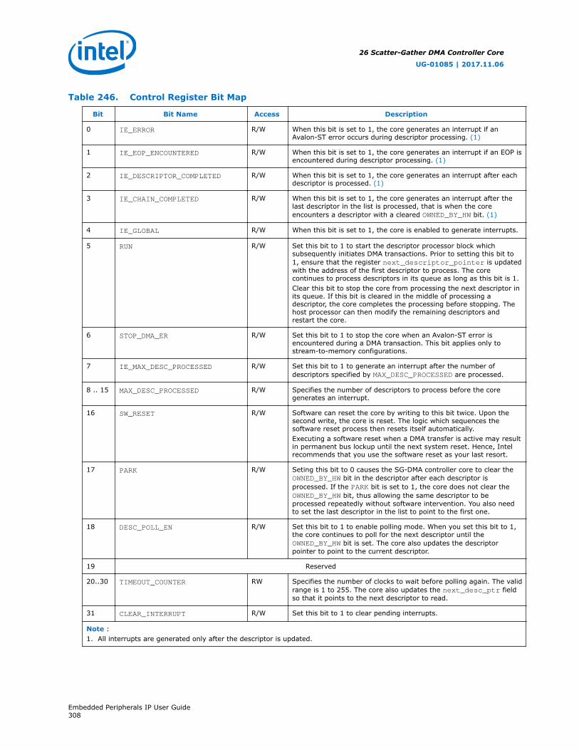
Table 246. Control Register Bit Map
Bit Bit Name Access Description
0 IE_ERROR R/W When this bit is set to 1, the core generates an interrupt if anAvalon-ST error occurs during descriptor processing. (1)
1 IE_EOP_ENCOUNTERED R/W When this bit is set to 1, the core generates an interrupt if an EOP isencountered during descriptor processing. (1)
2 IE_DESCRIPTOR_COMPLETED R/W When this bit is set to 1, the core generates an interrupt after eachdescriptor is processed. (1)
3 IE_CHAIN_COMPLETED R/W When this bit is set to 1, the core generates an interrupt after thelast descriptor in the list is processed, that is when the coreencounters a descriptor with a cleared OWNED_BY_HW bit. (1)
4 IE_GLOBAL R/W When this bit is set to 1, the core is enabled to generate interrupts.
5 RUN R/W Set this bit to 1 to start the descriptor processor block whichsubsequently initiates DMA transactions. Prior to setting this bit to1, ensure that the register next_descriptor_pointer is updatedwith the address of the first descriptor to process. The corecontinues to process descriptors in its queue as long as this bit is 1.Clear this bit to stop the core from processing the next descriptor inits queue. If this bit is cleared in the middle of processing adescriptor, the core completes the processing before stopping. Thehost processor can then modify the remaining descriptors andrestart the core.
6 STOP_DMA_ER R/W Set this bit to 1 to stop the core when an Avalon-ST error isencountered during a DMA transaction. This bit applies only tostream-to-memory configurations.
7 IE_MAX_DESC_PROCESSED R/W Set this bit to 1 to generate an interrupt after the number ofdescriptors specified by MAX_DESC_PROCESSED are processed.
8 .. 15 MAX_DESC_PROCESSED R/W Specifies the number of descriptors to process before the coregenerates an interrupt.
16 SW_RESET R/W Software can reset the core by writing to this bit twice. Upon thesecond write, the core is reset. The logic which sequences thesoftware reset process then resets itself automatically.Executing a software reset when a DMA transfer is active may resultin permanent bus lockup until the next system reset. Hence, Intelrecommends that you use the software reset as your last resort.
17 PARK R/W Seting this bit to 0 causes the SG-DMA controller core to clear theOWNED_BY_HW bit in the descriptor after each descriptor isprocessed. If the PARK bit is set to 1, the core does not clear theOWNED_BY_HW bit, thus allowing the same descriptor to beprocessed repeatedly without software intervention. You also needto set the last descriptor in the list to point to the first one.
18 DESC_POLL_EN R/W Set this bit to 1 to enable polling mode. When you set this bit to 1,the core continues to poll for the next descriptor until theOWNED_BY_HW bit is set. The core also updates the descriptorpointer to point to the current descriptor.
19 Reserved
20..30 TIMEOUT_COUNTER RW Specifies the number of clocks to wait before polling again. The validrange is 1 to 255. The core also updates the next_desc_ptr fieldso that it points to the next descriptor to read.
31 CLEAR_INTERRUPT R/W Set this bit to 1 to clear pending interrupts.
Note :1. All interrupts are generated only after the descriptor is updated.
26 Scatter-Gather DMA Controller Core
UG-01085 | 2017.11.06
Embedded Peripherals IP User Guide308
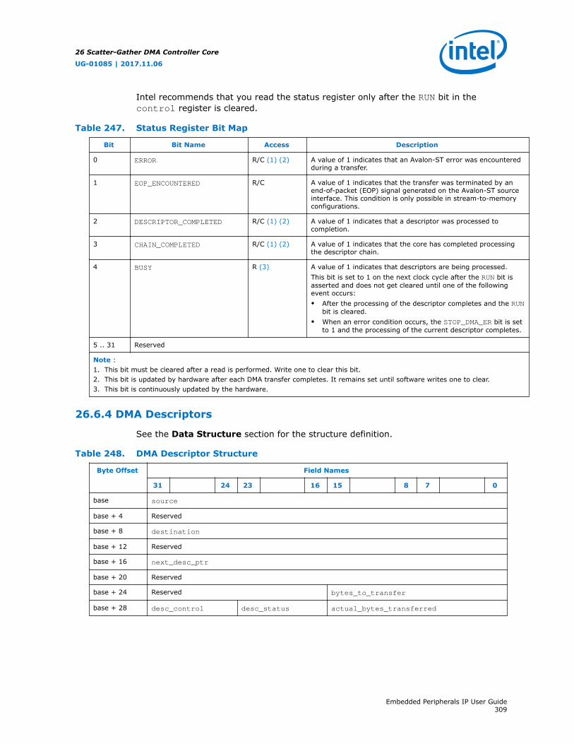
Intel recommends that you read the status register only after the RUN bit in thecontrol register is cleared.
Table 247. Status Register Bit Map
Bit Bit Name Access Description
0 ERROR R/C (1) (2) A value of 1 indicates that an Avalon-ST error was encounteredduring a transfer.
1 EOP_ENCOUNTERED R/C A value of 1 indicates that the transfer was terminated by anend-of-packet (EOP) signal generated on the Avalon-ST sourceinterface. This condition is only possible in stream-to-memoryconfigurations.
2 DESCRIPTOR_COMPLETED R/C (1) (2) A value of 1 indicates that a descriptor was processed tocompletion.
3 CHAIN_COMPLETED R/C (1) (2) A value of 1 indicates that the core has completed processingthe descriptor chain.
4 BUSY R (3) A value of 1 indicates that descriptors are being processed.This bit is set to 1 on the next clock cycle after the RUN bit isasserted and does not get cleared until one of the followingevent occurs:• After the processing of the descriptor completes and the RUN
bit is cleared.• When an error condition occurs, the STOP_DMA_ER bit is set
to 1 and the processing of the current descriptor completes.
5 .. 31 Reserved
Note :1. This bit must be cleared after a read is performed. Write one to clear this bit.2. This bit is updated by hardware after each DMA transfer completes. It remains set until software writes one to clear.3. This bit is continuously updated by the hardware.
26.6.4 DMA Descriptors
See the Data Structure section for the structure definition.
Table 248. DMA Descriptor Structure
Byte Offset Field Names
31 24 23 16 15 8 7 0
base source
base + 4 Reserved
base + 8 destination
base + 12 Reserved
base + 16 next_desc_ptr
base + 20 Reserved
base + 24 Reserved bytes_to_transfer
base + 28 desc_control desc_status actual_bytes_transferred
26 Scatter-Gather DMA Controller Core
UG-01085 | 2017.11.06
Embedded Peripherals IP User Guide309
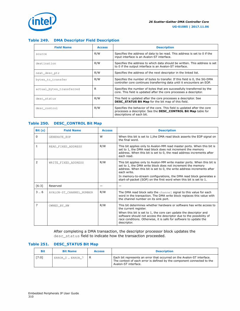
Table 249. DMA Descriptor Field Description
Field Name Access Description
source R/W Specifies the address of data to be read. This address is set to 0 if theinput interface is an Avalon-ST interface.
destination R/W Specifies the address to which data should be written. This address is setto 0 if the output interface is an Avalon-ST interface.
next_desc_ptr R/W Specifies the address of the next descriptor in the linked list.
bytes_to_transfer R/W Specifies the number of bytes to transfer. If this field is 0, the SG-DMAcontroller core continues transferring data until it encounters an EOP.
actual_bytes_transferred R Specifies the number of bytes that are successfully transferred by thecore. This field is updated after the core processes a descriptor.
desc_status R/W This field is updated after the core processes a descriptor. SeeDESC_STATUS Bit Map for the bit map of this field.
desc_control R/W Specifies the behavior of the core. This field is updated after the coreprocesses a descriptor. See the DESC_CONTROL Bit Map table fordescriptions of each bit.
Table 250. DESC_CONTROL Bit Map
Bit (s) Field Name Access Description
0 GENERATE_EOP W When this bit is set to 1,the DMA read block asserts the EOP signal onthe final word.
1 READ_FIXED_ADDRESS R/W This bit applies only to Avalon-MM read master ports. When this bit isset to 1, the DMA read block does not increment the memoryaddress. When this bit is set to 0, the read address increments aftereach read.
2 WRITE_FIXED_ADDRESS R/W This bit applies only to Avalon-MM write master ports. When this bit isset to 1, the DMA write block does not increment the memoryaddress. When this bit is set to 0, the write address increments aftereach write.In memory-to-stream configurations, the DMA read block generates astart-of-packet (SOP) on the first word when this bit is set to 1.
[6:3] Reserved — —
3 .. 6 AVALON-ST_CHANNEL_NUMBER R/W The DMA read block sets the channel signal to this value for eachword in the transaction. The DMA write block replaces this value withthe channel number on its sink port.
7 OWNED_BY_HW R/W This bit determines whether hardware or software has write access tothe current register.When this bit is set to 1, the core can update the descriptor andsoftware should not access the descriptor due to the possibility ofrace conditions. Otherwise, it is safe for software to update thedescriptor.
After completing a DMA transaction, the descriptor processor block updates thedesc_status field to indicate how the transaction proceeded.
Table 251. DESC_STATUS Bit Map
Bit Bit Name Access Description
[7:0] ERROR_0 .. ERROR_7 R Each bit represents an error that occurred on the Avalon-ST interface.The context of each error is defined by the component connected to theAvalon-ST interface.
26 Scatter-Gather DMA Controller Core
UG-01085 | 2017.11.06
Embedded Peripherals IP User Guide310

26.6.5 Timeouts
The SG-DMA controller does not implement internal counters to detect stalls. Softwarecan instantiate a timer component if this functionality is required.
26.7 Programming with SG-DMA Controller
This section describes the device and descriptor data structures, and the applicationprogramming interface (API) for the SG-DMA controller core.
26.7.1 Data Structure
Table 252. Device Data Structure
typedef struct alt_sgdma_dev{alt_llist llist; // Device linked-list entryconst char *name; // Name of SGDMA in SOPC Systemvoid *base; // Base address of SGDMAalt_u32 *descriptor_base; // reservedalt_u32 next_index; // reservedalt_u32 num_descriptors; // reservedalt_sgdma_descriptor *current_descriptor; // reservedalt_sgdma_descriptor *next_descriptor; // reservedalt_avalon_sgdma_callback callback; // Callback routine pointervoid *callback_context; // Callback context pointeralt_u32 chain_control; // Value OR'd into control reg} alt_sgdma_dev;
Table 253. Descriptor Data Structure
typedef struct {alt_u32 *read_addr;alt_u32 read_addr_pad;alt_u32 *write_addr;alt_u32 write_addr_pad;alt_u32 *next;alt_u32 next_pad;alt_u16 bytes_to_transfer;alt_u8 read_burst; /* Reserved field. Set to 0. */alt_u8 write_burst;/* Reserved field. Set to 0. */alt_u16 actual_bytes_transferred;alt_u8 status;alt_u8 control;} alt_avalon_sgdma_packed alt_sgdma_descriptor;
26 Scatter-Gather DMA Controller Core
UG-01085 | 2017.11.06
Embedded Peripherals IP User Guide311
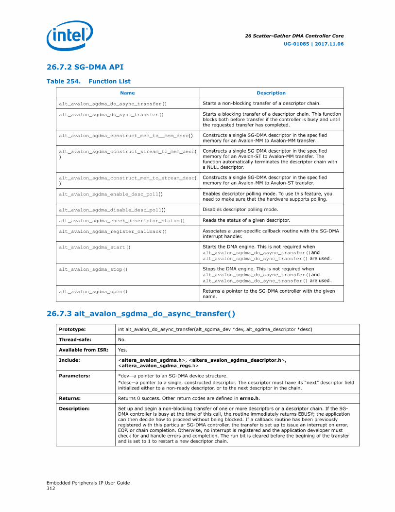
26.7.2 SG-DMA API
Table 254. Function List
Name Description
alt_avalon_sgdma_do_async_transfer() Starts a non-blocking transfer of a descriptor chain.
alt_avalon_sgdma_do_sync_transfer() Starts a blocking transfer of a descriptor chain. This functionblocks both before transfer if the controller is busy and untilthe requested transfer has completed.
alt_avalon_sgdma_construct_mem_to__mem_desc() Constructs a single SG-DMA descriptor in the specifiedmemory for an Avalon-MM to Avalon-MM transfer.
alt_avalon_sgdma_construct_stream_to_mem_desc()
Constructs a single SG-DMA descriptor in the specifiedmemory for an Avalon-ST to Avalon-MM transfer. Thefunction automatically terminates the descriptor chain witha NULL descriptor.
alt_avalon_sgdma_construct_mem_to_stream_desc()
Constructs a single SG-DMA descriptor in the specifiedmemory for an Avalon-MM to Avalon-ST transfer.
alt_avalon_sgdma_enable_desc_poll() Enables descriptor polling mode. To use this feature, youneed to make sure that the hardware supports polling.
alt_avalon_sgdma_disable_desc_poll() Disables descriptor polling mode.
alt_avalon_sgdma_check_descriptor_status() Reads the status of a given descriptor.
alt_avalon_sgdma_register_callback() Associates a user-specific callback routine with the SG-DMAinterrupt handler.
alt_avalon_sgdma_start() Starts the DMA engine. This is not required whenalt_avalon_sgdma_do_async_transfer()andalt_avalon_sgdma_do_sync_transfer() are used.
alt_avalon_sgdma_stop() Stops the DMA engine. This is not required whenalt_avalon_sgdma_do_async_transfer()andalt_avalon_sgdma_do_sync_transfer() are used.
alt_avalon_sgdma_open() Returns a pointer to the SG-DMA controller with the givenname.
26.7.3 alt_avalon_sgdma_do_async_transfer()
Prototype: int alt_avalon_do_async_transfer(alt_sgdma_dev *dev, alt_sgdma_descriptor *desc)
Thread-safe: No.
Available from ISR: Yes.
Include: <altera_avalon_sgdma.h>, <altera_avalon_sgdma_descriptor.h>,<altera_avalon_sgdma_regs.h>
Parameters: *dev—a pointer to an SG-DMA device structure.*desc—a pointer to a single, constructed descriptor. The descriptor must have its “next” descriptor fieldinitialized either to a non-ready descriptor, or to the next descriptor in the chain.
Returns: Returns 0 success. Other return codes are defined in errno.h.
Description: Set up and begin a non-blocking transfer of one or more descriptors or a descriptor chain. If the SG-DMA controller is busy at the time of this call, the routine immediately returns EBUSY; the applicationcan then decide how to proceed without being blocked. If a callback routine has been previouslyregistered with this particular SG-DMA controller, the transfer is set up to issue an interrupt on error,EOP, or chain completion. Otherwise, no interrupt is registered and the application developer mustcheck for and handle errors and completion. The run bit is cleared before the begining of the transferand is set to 1 to restart a new descriptor chain.
26 Scatter-Gather DMA Controller Core
UG-01085 | 2017.11.06
Embedded Peripherals IP User Guide312
26.7.4 alt_avalon_sgdma_do_sync_transfer()
Prototype: alt_u8 alt_avalon_sgdma_do_sync_transfer(alt_sgdma_dev *dev, alt_sgdma_descriptor *desc)
Thread-safe: No.
Available from ISR: Not recommended.
Include: <altera_avalon_sgdma.h>, <altera_avalon_sgdma_descriptor.h>,<altera_avalon_sgdma_regs.h>
Parameters: *dev—a pointer to an SG-DMA device structure.*desc—a pointer to a single, constructed descriptor. The descriptor must have its “next” descriptor fieldinitialized either to a non-ready descriptor, or to the next descriptor in the chain.
Returns: Returns the contents of the status register.
Description: Sends a fully formed descriptor or list of descriptors to the SG-DMA controller for transfer. This functionblocks both before transfer, if the SG-DMA controller is busy, and until the requested transfer hascompleted. If an error is detected during the transfer, it is abandoned and the controller’s status registercontents are returned to the caller. Additional error information is available in the status bits of eachdescriptor that the SG-DMA processed. The user application searches through the descriptor or list ofdescriptors to gather specific error information. The run bit is cleared before the begining of the transferand is set to 1 to restart a new descriptor chain.
26.7.5 alt_avalon_sgdma_construct_mem_to_mem_desc()
Prototype: void alt_avalon_sgdma_construct_mem_to_mem_desc(alt_sgdma_descriptor *desc,alt_sgdma_descriptor *next, alt_u32 *read_addr, alt_u32 *write_addr, alt_u16 length, int read_fixed,int write_fixed)
Thread-safe: Yes.
Available from ISR: Yes.
Include: <altera_avalon_sgdma.h>, <altera_avalon_sgdma_descriptor.h>,<altera_avalon_sgdma_regs.h>
Parameters: *desc—a pointer to the descriptor being constructed.*next—a pointer to the “next” descriptor. This does not need to be a complete or functional descriptor,but must be properly allocated.*read_addr—the first read address for the SG-DMA transfer.*write_addr—the first write address for the SG-DMA transfer.length—the number of bytes for the transfer.read_fixed—if non-zero, the SG-DMA reads from a fixed address.write_fixed—if non-zero, the SG-DMA writes to a fixed address.
Returns: void
Description: This function constructs a single SG-DMA descriptor in the memory specified inalt_avalon_sgdma_descriptor *desc for an Avalon-MM to Avalon-MM transfer. The function setsthe OWNED_BY_HW bit in the descriptor's control field, marking the completed descriptor as ready torun. The descriptor is processed when the SG-DMA controller receives the descriptor and the RUN bit is1.The next field of the descriptor being constructed is set to the address in *next. The OWNED_BY_HWbit of the descriptor at *next is explicitly cleared. Once the SG-DMA completes processing of the *desc,it does not process the descriptor at *next until its OWNED_BY_HW bit is set. To create a descriptorchain, you can repeatedly call this function using the previous call's *next pointer in the *descparameter.You must properly allocate memory for the creation of both the descriptor under construction as well asthe next descriptor in the chain.Descriptors must be in a memory device mastered by the SG-DMA controller’s chain read and chainwrite Avalon master ports. Care must be taken to ensure that both *desc and *next point to areas ofmemory mastered by the controller.
26 Scatter-Gather DMA Controller Core
UG-01085 | 2017.11.06
Embedded Peripherals IP User Guide313
26.7.6 alt_avalon_sgdma_construct_stream_to_mem_desc()
Prototype: void alt_avalon_sgdma_construct_stream_to_mem_desc(alt_sgdma_descriptor *desc,alt_sgdma_descriptor *next, alt_u32 *write_addr, alt_u16 length_or_eop, int write_fixed)
Thread-safe: Yes.
Available from ISR: Yes.
Include: <altera_avalon_sgdma.h>, <altera_avalon_sgdma_descriptor.h>,<altera_avalon_sgdma_regs.h>
Parameters: *desc—a pointer to the descriptor being constructed.*next—a pointer to the “next” descriptor. This does not need to be a complete or functional descriptor,but must be properly allocated.*write_addr—the first write address for the SG-DMA transfer.length_or_eop—the number of bytes for the transfer. If set to zero (0x0), the transfer continues until anEOP signal is received from the Avalon-ST interface.write_fixed—if non-zero, the SG-DMA will write to a fixed address.
Returns: void
Description: This function constructs a single SG-DMA descriptor in the memory specified inalt_avalon_sgdma_descriptor *desc for an Avalon-ST to Avalon-MM transfer. The source (read)data for the transfer comes from the Avalon-ST interface connected to the SG-DMA controller'sstreaming read port.The function sets the OWNED_BY_HW bit in the descriptor's control field, marking the completeddescriptor as ready to run. The descriptor is processed when the SG-DMA controller receives thedescriptor and the RUN bit is 1.The next field of the descriptor being constructed is set to the address in *next. The OWNED_BY_HW bitof the descriptor at *next is explicitly cleared. Once the SG-DMA completes processing of the *desc, itdoes not process the descriptor at *next until its OWNED_BY_HW bit is set. To create a descriptor chain,you can repeatedly call this function using the previous call's *next pointer in the *desc parameter.You must properly allocate memory for the creation of both the descriptor under construction as well asthe next descriptor in the chain.Descriptors must be in a memory device mastered by the SG-DMA controller’s chain read and chainwrite Avalon master ports. Care must be taken to ensure that both *desc and *next point to areas ofmemory mastered by the controller.
26.7.7 alt_avalon_sgdma_construct_mem_to_stream_desc()
Prototype: void alt_avalon_sgdma_construct_mem_to_stream_desc(alt_sgdma_descriptor *desc,alt_sgdma_descriptor *next, alt_u32 *read_addr, alt_u16 length, int read_fixed, int generate_sop, intgenerate_eop, alt_u8 atlantic_channel)
Thread-safe: Yes.
Available from ISR: Yes.
Include: <altera_avalon_sgdma.h>, <altera_avalon_sgdma_descriptor.h>,<altera_avalon_sgdma_regs.h>
Parameters: *desc—a pointer to the descriptor being constructed.*next—a pointer to the “next” descriptor. This does not need to be a complete or functional descriptor,but must be properly allocated.*read_addr—the first read address for the SG-DMA transfer.length—the number of bytes for the transfer.read_fixed—if non-zero, the SG-DMA reads from a fixed address.generate_sop—if non-zero, the SG-DMA generates a SOP on the Avalon-ST interface when commencingthe transfer.generate_eop—if non-zero, the SG-DMA generates an EOP on the Avalon-ST interface when completingthe transfer.
continued...
26 Scatter-Gather DMA Controller Core
UG-01085 | 2017.11.06
Embedded Peripherals IP User Guide314

atlantic_channel—an 8-bit Avalon-ST channel number. Channels are currently not supported. Set thisparameter to 0.
Returns: void
Description: This function constructs a single SG-DMA descriptor in the memory specified in alt_avalon_sgdma-descriptor *desc for an Avalon-MM to Avalon-ST transfer. The destination (write) data for the transfergoes to the Avalon-ST interface connected to the SG-DMA controller's streaming write port. The functionsets the OWNED_BY_HW bit in the descriptor's control field, marking the completed descriptor as readyto run. The descriptor is processed when the SG-DMA controller receives the descriptor and the RUN bitis 1.The next field of the descriptor being constructed is set to the address in *next. The OWNED_BY_HW bitof the descriptor at *next is explicitly cleared. Once the SG-DMA completes processing of the *desc, itdoes not process the descriptor at *next until its OWNED_BY_HW bit is set. To create a descriptor chain,you can repeatedly call this function using the previous call's *next pointer in the *desc parameter.You are responsible for properly allocating memory for the creation of both the descriptor underconstruction as well as the next descriptor in the chain. Descriptors must be in a memory devicemastered by the SG-DMA controller’s chain read and chain write Avalon master ports. Care must betaken to ensure that both *desc and *next point to areas of memory mastered by the controller.
26.7.8 alt_avalon_sgdma_enable_desc_poll()
Prototype: void alt_avalon_sgdma_enable_desc_poll(alt_sgdma_dev *dev, alt_u32 frequency)
Thread-safe: Yes.
Available from ISR: Yes.
Include: <altera_avalon_sgdma.h>, <altera_avalon_sgdma_descriptor.h>,<altera_avalon_sgdma_regs.h>*dev—a pointer to an SG-DMA device structure.
Parameters: frequency—the frequency value to set. Only the lower 11-bit value of the frequency is written to thecontrol register.
Returns: void
Description: Enables descriptor polling mode with a specific frequency. There is no effect if the hardware does notsupport this mode.
26.7.9 alt_avalon_sgdma_disable_desc_poll()
Prototype: void alt_avalon_sgdma_disable_desc_poll(alt_sgdma_dev *dev)
Thread-safe: Yes.
Available from ISR: Yes.
Include: <altera_avalon_sgdma.h>, <altera_avalon_sgdma_descriptor.h>,<altera_avalon_sgdma_regs.h>
Parameters: *dev—a pointer to an SG-DMA device structure.
Returns: void
Description: Disables descriptor polling mode.
26.7.10 alt_avalon_sgdma_check_descriptor_status()
Prototype: int alt_avalon_sgdma_check_descriptor_status(alt_sgdma_descriptor *desc)
Thread-safe: Yes.
Available from ISR: Yes.
continued...
26 Scatter-Gather DMA Controller Core
UG-01085 | 2017.11.06
Embedded Peripherals IP User Guide315

Include: <altera_avalon_sgdma.h>, <altera_avalon_sgdma_descriptor.h>,<altera_avalon_sgdma_regs.h>
Parameters: *desc—a pointer to the constructed descriptor to examine.
Returns: Returns 0 if the descriptor is error-free, not owned by hardware, or a previously requested transfercompleted normally. Other return codes are defined in errno.h.
Description: Checks a descriptor previously owned by hardware for any errors reported in a previous transfer. Theroutine reports: errors reported by the SG-DMA controller, the buffer in use.
26.7.11 alt_avalon_sgdma_register_callback()
Prototype: void alt_avalon_sgdma_register_callback(alt_sgdma_dev *dev, alt_avalon_sgdma_callback callback,alt_u16 chain_control, void *context)
Thread-safe: Yes.
Available from ISR: Yes.
Include: <altera_avalon_sgdma.h>, <altera_avalon_sgdma_descriptor.h>,<altera_avalon_sgdma_regs.h>
Parameters: *dev—a pointer to the SG-DMA device structure.callback—a pointer to the callback routine to execute at interrupt level.chain_control—the SG-DMA control register contents.*context—a pointer used to pass context-specific information to the ISR. context can point to any ISR-specific information.
Returns: void
Description: Associates a user-specific routine with the SG-DMA interrupt handler. If a callback is registered, all non-blocking transfers enables interrupts that causes the callback to be executed. The callback runs as partof the interrupt service routine, and care must be taken to follow the guidelines for acceptable interruptservice routine behavior as described in the Nios II Software Developer’s Handbook.To disable callbacks after registering one, call this routine with 0x0 as the callback argument.
26.7.12 alt_avalon_sgdma_start()
Prototype: void alt_avalon_sgdma_start(alt_sgdma_dev *dev)
Thread-safe: No.
Available from ISR: Yes.
Include: <altera_avalon_sgdma.h>, <altera_avalon_sgdma_descriptor.h>,<altera_avalon_sgdma_regs.h>
Parameters: *dev—a pointer to the SG-DMA device structure.
Returns: void
Description: Starts the DMA engine and processes the descriptor pointed to in the controller's next descriptor pointerand all subsequent descriptors in the chain. It is not necessary to call this function when do_sync ordo_async is used.
26.7.13 alt_avalon_sgdma_stop()
Prototype: void alt_avalon_sgdma_stop(alt_sgdma_dev *dev)
Thread-safe: No.
Available from ISR: Yes.
continued...
26 Scatter-Gather DMA Controller Core
UG-01085 | 2017.11.06
Embedded Peripherals IP User Guide316

Include: <altera_avalon_sgdma.h>, <altera_avalon_sgdma_descriptor.h>,<altera_avalon_sgdma_regs.h>
Parameters: *dev—a pointer to the SG-DMA device structure.
Returns: void
Description: Stops the DMA engine following completion of the current buffer descriptor. It is not necessary to callthis function when do_sync or do_async is used.
26.7.14 alt_avalon_sgdma_open()
Prototype: alt_sgdma_dev* alt_avalon_sgdma_open(const char* name)
Thread-safe: Yes.
Available from ISR: No.
Include: <altera_avalon_sgdma.h>, <altera_avalon_sgdma_descriptor.h>,<altera_avalon_sgdma_regs.h>
Parameters: name—the name of the SG-DMA device to open.
Returns: A pointer to the SG-DMA device structure associated with the supplied name, or NULL if nocorresponding SG-DMA device structure was found.
Description: Retrieves a pointer to a hardware SG-DMA device structure.
26.8 Document Revision History
Table 255. Scatter-Gather DMA Controller Core Revision History
Date Version Changes
October 2015 2015.10.30 Updated sections:• Register Maps: "Control Register Bit Map" table• SG-DMA API: "Function List" tableAdded sections:• alt_avalon_sgdma_enable_desc_poll()• alt_avalon_sgdma_disable_desc_poll()
July 2014 2014.07.24 Updated Register Maps table, included version register
December 2010 v10.1.0 Updated figure 19-4 and figure 19-5.Revised the bit description of IE_GLOBAL in table 19-7.Removed the “Device Support”, “Instantiating the Core in SOPC Builder”,and “Referenced Documents” sections.
July 2010 v10.0.0 No change from previous release.
November 2009 v9.1.0 Revised descriptions of register fields and bits.Added description to the memory-to-stream configurations.Added descriptions to alt_avalon_sgdma_do_sync_transfer() andalt_avalon_sgdma_do_async_transfer() API.Added a list on error signals implementation.
March 2009 v9.0.0 Added description of Enable bursting on descriptor read master.
November 2008 v8.1.0 Changed to 8-1/2 x 11 page size.Added section DMA Descriptors in Functional SpecificationsRevised descriptions of register fields and bits.Reorganized sections Software Programming Model and Programming withSG-DMA Controller Core.
May 2008 v8.0.0 Added sections on burst transfers.
26 Scatter-Gather DMA Controller Core
UG-01085 | 2017.11.06
Embedded Peripherals IP User Guide317
27 SDRAM Controller Core
27.1 Core Overview
The SDRAM controller core with Avalon interface provides an Avalon Memory-Mapped(Avalon-MM) interface to off-chip SDRAM. The SDRAM controller allows designers tocreate custom systems in an Intel FPGA device that connect easily to SDRAM chips.The SDRAM controller supports standard SDRAM as described in the PC100specification.
SDRAM is commonly used in cost-sensitive applications requiring large amounts ofvolatile memory. While SDRAM is relatively inexpensive, control logic is required toperform refresh operations, open-row management, and other delays and commandsequences. The SDRAM controller connects to one or more SDRAM chips, and handlesall SDRAM protocol requirements. Internal to the device, the core presents an Avalon-MM slave port that appears as linear memory (flat address space) to Avalon-MMmaster peripherals.
The core can access SDRAM subsystems with various data widths (8, 16, 32, or64 bits), various memory sizes, and multiple chip selects. The Avalon-MM interface islatency-aware, allowing read transfers to be pipelined. The core can optionally shareits address and data buses with other off-chip Avalon-MM tri-state devices. Thisfeature is valuable in systems that have limited I/O pins, yet must connect to multiplememory chips in addition to SDRAM.
27.2 Functional Description
The diagram below shows a block diagram of the SDRAM controller core connected toan external SDRAM chip.
UG-01085 | 2017.11.06
Intel Corporation. All rights reserved. Intel, the Intel logo, Altera, Arria, Cyclone, Enpirion, MAX, Nios, Quartusand Stratix words and logos are trademarks of Intel Corporation or its subsidiaries in the U.S. and/or othercountries. Intel warrants performance of its FPGA and semiconductor products to current specifications inaccordance with Intel's standard warranty, but reserves the right to make changes to any products and servicesat any time without notice. Intel assumes no responsibility or liability arising out of the application or use of anyinformation, product, or service described herein except as expressly agreed to in writing by Intel. Intelcustomers are advised to obtain the latest version of device specifications before relying on any publishedinformation and before placing orders for products or services.*Other names and brands may be claimed as the property of others.
ISO9001:2008Registered
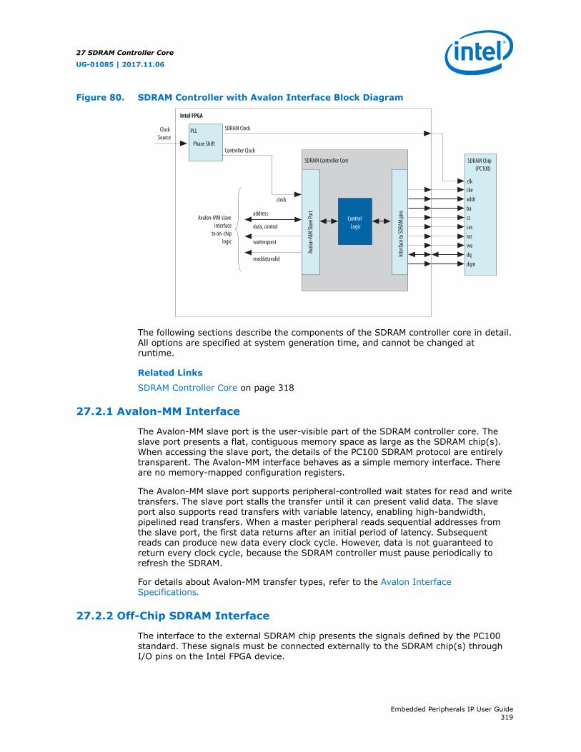
Figure 80. SDRAM Controller with Avalon Interface Block Diagram
Avalon-MM slaveinterface
to on-chiplogic
SDRAM Controller Core
data, control
Avalo
n-MM
Slav
e Por
t
clock
waitrequest
readdatavaliddqdqm
PLL
Phase Shift
Inter
face t
o SDR
AM pi
ns
Intel FPGA
clk
addr
rascascs
cke
ba
we
ControlLogic
address
SDRAM Clock
Controller Clock
ClockSource
SDRAM Chip(PC100)
The following sections describe the components of the SDRAM controller core in detail.All options are specified at system generation time, and cannot be changed atruntime.
Related Links
SDRAM Controller Core on page 318
27.2.1 Avalon-MM Interface
The Avalon-MM slave port is the user-visible part of the SDRAM controller core. Theslave port presents a flat, contiguous memory space as large as the SDRAM chip(s).When accessing the slave port, the details of the PC100 SDRAM protocol are entirelytransparent. The Avalon-MM interface behaves as a simple memory interface. Thereare no memory-mapped configuration registers.
The Avalon-MM slave port supports peripheral-controlled wait states for read and writetransfers. The slave port stalls the transfer until it can present valid data. The slaveport also supports read transfers with variable latency, enabling high-bandwidth,pipelined read transfers. When a master peripheral reads sequential addresses fromthe slave port, the first data returns after an initial period of latency. Subsequentreads can produce new data every clock cycle. However, data is not guaranteed toreturn every clock cycle, because the SDRAM controller must pause periodically torefresh the SDRAM.
For details about Avalon-MM transfer types, refer to the Avalon InterfaceSpecifications.
27.2.2 Off-Chip SDRAM Interface
The interface to the external SDRAM chip presents the signals defined by the PC100standard. These signals must be connected externally to the SDRAM chip(s) throughI/O pins on the Intel FPGA device.
27 SDRAM Controller Core
UG-01085 | 2017.11.06
Embedded Peripherals IP User Guide319

27.2.2.1 Signal Timing and Electrical Characteristics
The timing and sequencing of signals depends on the configuration of the core. Thehardware designer configures the core to match the SDRAM chip chosen for thesystem. See the Configuration section for details. The electrical characteristics of thedevice pins depend on both the target device family and the assignments made in theIntel Quartus Prime software. Some device families support a wider range of electricalstandards, and therefore are capable of interfacing with a greater variety of SDRAMchips. For details, refer to the device handbook for the target device family.
27.2.2.2 Synchronizing Clock and Data Signals
The clock for the SDRAM chip (SDRAM clock) must be driven at the same frequency asthe clock for the Avalon-MM interface on the SDRAM controller (controller clock). As inall synchronous designs, you must ensure that address, data, and control signals atthe SDRAM pins are stable when a clock edge arrives. As shown in the above SDRAMController with Avalon Interface block diagram, you can use an on-chip phase-locked loop (PLL) to alleviate clock skew between the SDRAM controller core and theSDRAM chip. At lower clock speeds, the PLL might not be necessary. At higher clockrates, a PLL is necessary to ensure that the SDRAM clock toggles only when signalsare stable on the pins. The PLL block is not part of the SDRAM controller core. If a PLLis necessary, you must instantiate it manually. You can instantiate the PLL coreinterface or instantiate an ALTPLL IP core outside the Platform Designer systemmodule.
If you use a PLL, you must tune the PLL to introduce a clock phase shift so thatSDRAM clock edges arrive after synchronous signals have stabilized. See Clock, PLLand Timing Considerations sections for details.
For more information about instantiating a PLL, refer to PLL Cores chapter. The NiosII development tools provide example hardware designs that use the SDRAMcontroller core in conjunction with a PLL, which you can use as a reference for yourcustom designs.
The Nios II development tools are available free for download fromIntel FPGA website.
27.2.2.3 Clock Enable (CKE) not Supported
The SDRAM controller does not support clock-disable modes. The SDRAM controllerpermanently asserts the CKE signal on the SDRAM.
27.2.2.4 Sharing Pins with other Avalon-MM Tri-State Devices
If an Avalon-MM tri-state bridge is present, the SDRAM controller core can share pinswith the existing tri-state bridge. In this case, the core’s addr, dq (data) and dqm(byte-enable) pins are shared with other devices connected to the Avalon-MM tri-statebridge. This feature conserves I/O pins, which is valuable in systems that havemultiple external memory chips (for example, flash, SRAM, and SDRAM), but too fewpins to dedicate to the SDRAM chip. See Performance Considerations section fordetails about how pin sharing affects performance.
The SDRAM addresses must connect all address bits regardless of the size of the wordso that the low-order address bits on the tri-state bridge align with the low-orderaddress bits on the memory device. The Avalon-MM tristate address signal always
27 SDRAM Controller Core
UG-01085 | 2017.11.06
Embedded Peripherals IP User Guide320

presents a byte address. It is not possible to drop A0 of the tri-state bridge formemories when the smallest access size is 16 bits or A0-A1 of the tri-state bridgewhen the smallest access size is 32 bits.
27.2.3 Board Layout and Pinout Considerations
When making decisions about the board layout and device pinout, try to minimize theskew between the SDRAM signals. For example, when assigning the device pinout,group the SDRAM signals, including the SDRAM clock output, physically close together.Also, you can use the Fast Input Register and Fast Output Register logic optionsin the Intel Quartus Prime software. These logic options place registers for the SDRAMsignals in the I/O cells. Signals driven from registers in I/O cells have similar timingcharacteristics, such as tCO, tSU, and tH.
27.2.4 Performance Considerations
Under optimal conditions, the SDRAM controller core’s bandwidth approaches oneword per clock cycle. However, because of the overhead associated with refreshing theSDRAM, it is impossible to reach one word per clock cycle. Other factors affect thecore’s performance, as described in the following sections.
27.2.4.1 Open Row Management
SDRAM chips are arranged as multiple banks of memory, in which each bank iscapable of independent open-row address management. The SDRAM controller coretakes advantage of open-row management for a single bank. Continuous reads orwrites within the same row and bank operate at rates approaching one word per clock.Applications that frequently access different destination banks require extramanagement cycles to open and close rows.
27.2.4.2 Sharing Data and Address Pins
When the controller shares pins with other tri-state devices, average access timeusually increases and bandwidth decreases. When access to the tri-state bridge isgranted to other devices, the SDRAM incurs overhead to open and close rows.Furthermore, the SDRAM controller has to wait several clock cycles before it is grantedaccess again.
To maximize bandwidth, the SDRAM controller automatically maintains control of thetri-state bridge as long as back-to-back read or write transactions continue within thesame row and bank.
This behavior may degrade the average access time for other devices sharing theAvalon-MM tri-state bridge.
The SDRAM controller closes an open row whenever there is a break in back-to-backtransactions, or whenever a refresh transaction is required. As a result:
• The controller cannot permanently block access to other devices sharing the tri-state bridge.
• The controller is guaranteed not to violate the SDRAM’s row open time limit.
27 SDRAM Controller Core
UG-01085 | 2017.11.06
Embedded Peripherals IP User Guide321

27.2.4.3 Hardware Design and Target Device
The target device affects the maximum achievable clock frequency of a hardwaredesign. Certain device families achieve higher fMAX performance than other families.Furthermore, within a device family, faster speed grades achieve higher performance.The SDRAM controller core can achieve 100 MHz in Intel FPGA high-performancedevice families, such as Stratix series. However, the core might not achieve 100 MHzperformance in all Intel FPGA device families.
The fMAX performance also depends on the system design. The SDRAM controller clockcan also drive other logic in the system module, which might affect the maximumachievable frequency. For the SDRAM controller core to achieve fMAX performance of100 MHz, all components driven by the same clock must be designed for a 100 MHzclock rate, and timing analysis in the Intel Quartus Prime software must verify that theoverall hardware design is capable of 100 MHz operation.
27.3 Configuration
The SDRAM controller MegaWizard has two pages: Memory Profile and Timing. Thissection describes the options available on each page.
The Presets list offers several pre-defined SDRAM configurations as a convenience. Ifthe SDRAM subsystem on the target board matches one of the preset configurations,you can configure the SDRAM controller core easily by selecting the appropriate presetvalue. The following preset configurations are defined:
• Micron MT8LSDT1664HG module
• Four SDR100 8 MByte × 16 chips
• Single Micron MT48LC2M32B2-7 chip
• Single Micron MT48LC4M32B2-7 chip
• Single NEC D4564163-A80 chip (64 MByte × 16)
• Single Alliance AS4LC1M16S1-10 chip
• Single Alliance AS4LC2M8S0-10 chip
Selecting a preset configuration automatically changes values on the MemoryProfile and Timing tabs to match the specific configuration. Altering aconfiguration setting on any page changes the Preset value to custom.
27.3.1 Memory Profile Page
The Memory Profile page allows you to specify the structure of the SDRAMsubsystem such as address and data bus widths, the number of chip select signals,and the number of banks.
27 SDRAM Controller Core
UG-01085 | 2017.11.06
Embedded Peripherals IP User Guide322
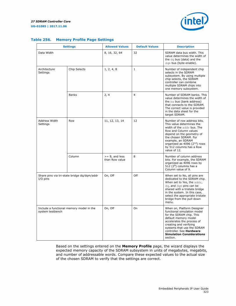
Table 256. Memory Profile Page Settings
Settings Allowed Values Default Values Description
Data Width 8, 16, 32, 64 32 SDRAM data bus width. Thisvalue determines the width ofthe dq bus (data) and thedqm bus (byte-enable).
ArchitectureSettings
Chip Selects 1, 2, 4, 8 1 Number of independent chipselects in the SDRAMsubsystem. By using multiplechip selects, the SDRAMcontroller can combinemultiple SDRAM chips intoone memory subsystem.
Banks 2, 4 4 Number of SDRAM banks. Thisvalue determines the width ofthe ba bus (bank address)that connects to the SDRAM.The correct value is providedin the data sheet for thetarget SDRAM.
Address WidthSettings
Row 11, 12, 13, 14 12 Number of row address bits.This value determines thewidth of the addr bus. TheRow and Column valuesdepend on the geometry ofthe chosen SDRAM. Forexample, an SDRAMorganized as 4096 (212) rowsby 512 columns has a Rowvalue of 12.
Column >= 8, and lessthan Row value
8 Number of column addressbits. For example, the SDRAMorganized as 4096 rows by512 (29) columns has aColumn value of 9.
Share pins via tri-state bridge dq/dqm/addrI/O pins
On, Off Off When set to No, all pins arededicated to the SDRAM chip.When set to Yes, the addr,dq, and dqm pins can beshared with a tristate bridgein the system. In this case,select the appropriate tristatebridge from the pull-downmenu.
Include a functional memory model in thesystem testbench
On, Off On When on, Platform Designerfunctional simulation modelfor the SDRAM chip. Thisdefault memory modelaccelerates the process ofcreating and verifyingsystems that use the SDRAMcontroller. See HardwareSimulation Considerationssection.
Based on the settings entered on the Memory Profile page, the wizard displays theexpected memory capacity of the SDRAM subsystem in units of megabytes, megabits,and number of addressable words. Compare these expected values to the actual sizeof the chosen SDRAM to verify that the settings are correct.
27 SDRAM Controller Core
UG-01085 | 2017.11.06
Embedded Peripherals IP User Guide323
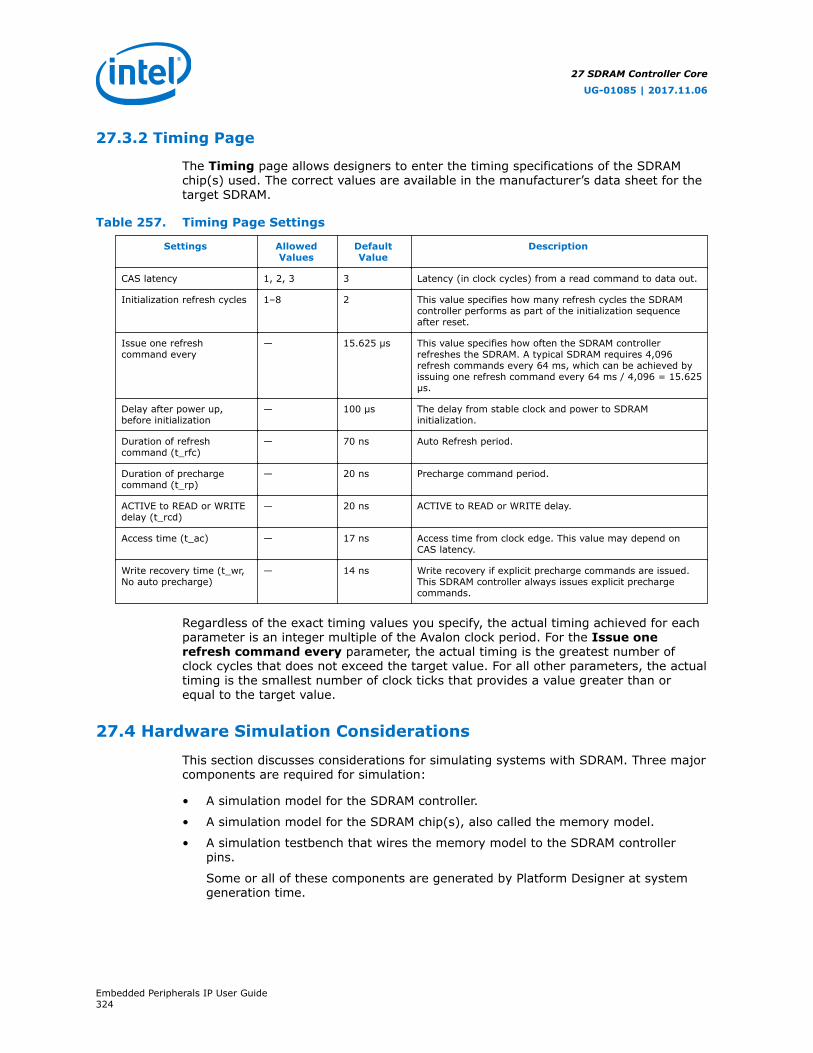
27.3.2 Timing Page
The Timing page allows designers to enter the timing specifications of the SDRAMchip(s) used. The correct values are available in the manufacturer’s data sheet for thetarget SDRAM.
Table 257. Timing Page Settings
Settings AllowedValues
DefaultValue
Description
CAS latency 1, 2, 3 3 Latency (in clock cycles) from a read command to data out.
Initialization refresh cycles 1–8 2 This value specifies how many refresh cycles the SDRAMcontroller performs as part of the initialization sequenceafter reset.
Issue one refreshcommand every
— 15.625 µs This value specifies how often the SDRAM controllerrefreshes the SDRAM. A typical SDRAM requires 4,096refresh commands every 64 ms, which can be achieved byissuing one refresh command every 64 ms / 4,096 = 15.625μs.
Delay after power up,before initialization
— 100 µs The delay from stable clock and power to SDRAMinitialization.
Duration of refreshcommand (t_rfc)
— 70 ns Auto Refresh period.
Duration of prechargecommand (t_rp)
— 20 ns Precharge command period.
ACTIVE to READ or WRITEdelay (t_rcd)
— 20 ns ACTIVE to READ or WRITE delay.
Access time (t_ac) — 17 ns Access time from clock edge. This value may depend onCAS latency.
Write recovery time (t_wr,No auto precharge)
— 14 ns Write recovery if explicit precharge commands are issued.This SDRAM controller always issues explicit prechargecommands.
Regardless of the exact timing values you specify, the actual timing achieved for eachparameter is an integer multiple of the Avalon clock period. For the Issue onerefresh command every parameter, the actual timing is the greatest number ofclock cycles that does not exceed the target value. For all other parameters, the actualtiming is the smallest number of clock ticks that provides a value greater than orequal to the target value.
27.4 Hardware Simulation Considerations
This section discusses considerations for simulating systems with SDRAM. Three majorcomponents are required for simulation:
• A simulation model for the SDRAM controller.
• A simulation model for the SDRAM chip(s), also called the memory model.
• A simulation testbench that wires the memory model to the SDRAM controllerpins.
Some or all of these components are generated by Platform Designer at systemgeneration time.
27 SDRAM Controller Core
UG-01085 | 2017.11.06
Embedded Peripherals IP User Guide324

27.4.1 SDRAM Controller Simulation Model
The SDRAM controller design files generated by Platform Designer are suitable forboth synthesis and simulation. Some simulation features are implemented in the HDLusing “translate on/off” synthesis directives that make certain sections of HDL codeinvisible to the synthesis tool.
The simulation features are implemented primarily for easy simulation of Nios andNios II processor systems using the ModelSim* simulator. The SDRAM controllersimulation model is not ModelSim specific. However, minor changes may be requiredto make the model work with other simulators.
If you change the simulation directives to create a custom simulation flow, be awarethat Platform Designer overwrites existing files during system generation. Takeprecautions to ensure your changes are not overwritten.
Refer to AN 351: Simulating Nios II Processor Designs for a demonstration ofsimulation of the SDRAM controller in the context of Nios II embedded processorsystems.
27.4.2 SDRAM Memory Model
This section describes the two options for simulating a memory model of the SDRAMchip(s).
27.4.2.1 Using the Generic Memory Model
If the Include a functional memory model the system testbench option isenabled at system generation, Platform Designer generates an HDL simulation modelfor the SDRAM memory. In the auto-generated system testbench, Platform Designerautomatically wires this memory model to the SDRAM controller pins.
Using the automatic memory model and testbench accelerates the process of creatingand verifying systems that use the SDRAM controller. However, the memory model is ageneric functional model that does not reflect the true timing or functionality of realSDRAM chips. The generic model is always structured as a single, monolithic block ofmemory. For example, even for a system that combines two SDRAM chips, the genericmemory model is implemented as a single entity.
27.4.2.2 Using the SDRAM Manufacturer's Memory Model
If the Include a functional memory model the system testbench option is notenabled, you are responsible for obtaining a memory model from the SDRAMmanufacturer, and manually wiring the model to the SDRAM controller pins in thesystem testbench.
27.5 Example Configurations
The following examples show how to connect the SDRAM controller outputs to anSDRAM chip or chips. The bus labeled ctl is an aggregate of the remaining signals,such as cas_n, ras_n, cke and we_n.
The address, data, and control signals are wired directly from the controller to thechip. The result is a 128-Mbit (16-Mbyte) memory space.
27 SDRAM Controller Core
UG-01085 | 2017.11.06
Embedded Peripherals IP User Guide325
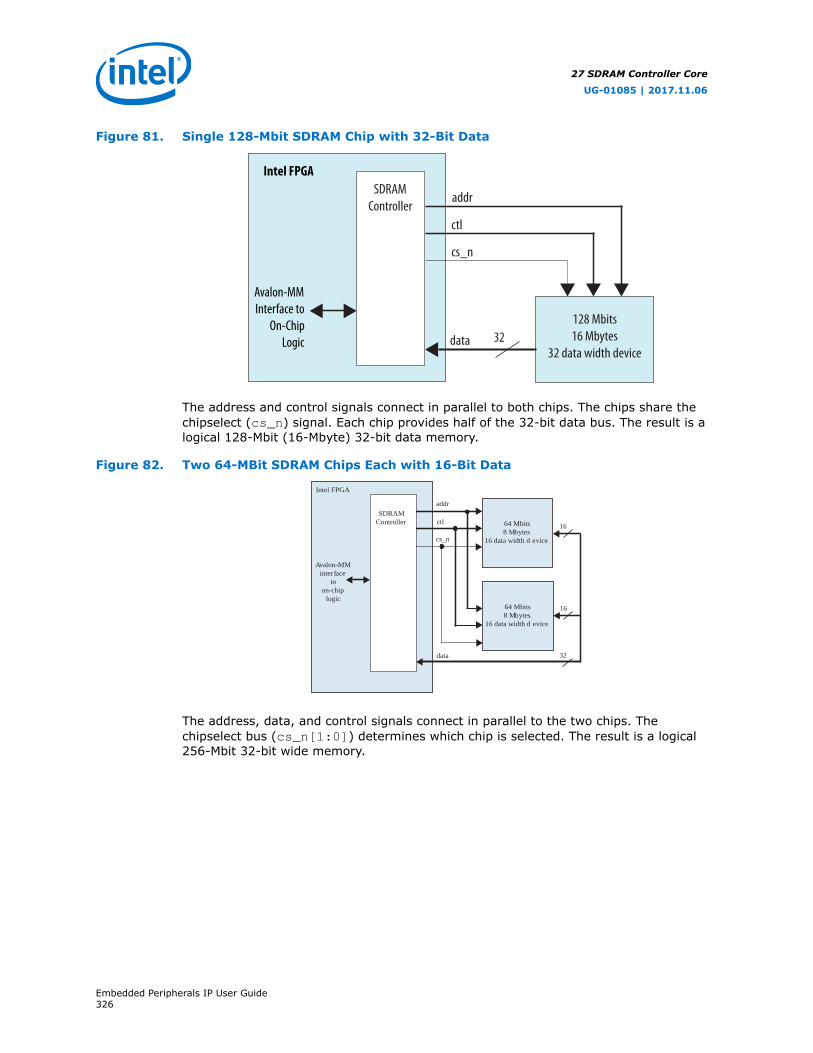
Figure 81. Single 128-Mbit SDRAM Chip with 32-Bit Data
data 32128 Mbits16 Mbytes
32 data width device
SDRAMController
addr
cs_n
ctl
Intel FPGA
Avalon-MMInterface to
On-ChipLogic
The address and control signals connect in parallel to both chips. The chips share thechipselect (cs_n) signal. Each chip provides half of the 32-bit data bus. The result is alogical 128-Mbit (16-Mbyte) 32-bit data memory.
Figure 82. Two 64-MBit SDRAM Chips Each with 16-Bit Data
addr
ctl
cs_n
SDRAMController
Intel FPGA
Avalon-MMinter face
toon-chip
logic
64 Mbits8 Mbytes
16 data width d evice
64 Mbits8 Mbytes
16 data width d evice
data
16
16
32
The address, data, and control signals connect in parallel to the two chips. Thechipselect bus (cs_n[1:0]) determines which chip is selected. The result is a logical256-Mbit 32-bit wide memory.
27 SDRAM Controller Core
UG-01085 | 2017.11.06
Embedded Peripherals IP User Guide326

Figure 83. Two 128-Mbit SDRAM Chips Each with 32-Bit Data
addr
ctl
cs_n [0]
cs_n [1]
SDRAMController
FPGA
Avalon-MMinter face
toon-chip
logic
data 32
128 Mbits16 Mbytes
32 data width d evice
128 Mbits16 Mbytes
32 data width d evice
32
32
27.6 Software Programming Model
The SDRAM controller behaves like simple memory when accessed via the Avalon-MMinterface. There are no software-configurable settings and no memory-mappedregisters. No software driver routines are required for a processor to access theSDRAM controller.
27.7 Clock, PLL and Timing Considerations
This section describes issues related to synchronizing signals from the SDRAMcontroller core with the clock that drives the SDRAM chip. During SDRAM transactions,the address, data, and control signals are valid at the SDRAM pins for a window oftime, during which the SDRAM clock must toggle to capture the correct values. Atslower clock frequencies, the clock naturally falls within the valid window. At higherfrequencies, you must compensate the SDRAM clock to align with the valid window.
Determine when the valid window occurs either by calculation or by analyzing theSDRAM pins with an oscilloscope. Then use a PLL to adjust the phase of the SDRAMclock so that edges occur in the middle of the valid window. Tuning the PLL mightrequire trial-and-error effort to align the phase shift to the properties of your targetboard.
For details about the PLL circuitry in your target device, refer to the appropriate devicefamily handbook.
For details about configuring the PLLs in Intel devices, refer to the ALTPLL IP CoreUser Guide.
27.7.1 Factors Affecting SDRAM Timing
The location and duration of the window depends on several factors:
27 SDRAM Controller Core
UG-01085 | 2017.11.06
Embedded Peripherals IP User Guide327

• Timing parameters of the device and SDRAM I/O pins — I/O timing parametersvary based on device family and speed grade.
• Pin location on the device — I/O pins connected to row routing have differenttiming than pins connected to column routing.
• Logic options used during the Intel Quartus Prime compilation — Logic optionssuch as the Fast Input Register and Fast Output Register logic affect thedesign fit. The location of logic and registers inside the device affects thepropagation delays of signals to the I/O pins.
• SDRAM CAS latency
As a result, the valid window timing is different for different combinations of FPGAand SDRAM devices. The window depends on the Intel Quartus Prime softwarefitting results and pin assignments.
27.7.2 Symptoms of an Untuned PLL
Detecting when the PLL is not tuned correctly might be difficult. Data transfers to orfrom the SDRAM might not fail universally. For example, individual transfers to theSDRAM controller might succeed, whereas burst transfers fail. For processor-basedsystems, if software can perform read or write data to SDRAM, but cannot run whenthe code is located in SDRAM, the PLL is probably tuned incorrectly.
27.7.3 Estimating the Valid Signal Window
This section describes how to estimate the location and duration of the valid signalwindow using timing parameters provided in the SDRAM datasheet and the IntelQuartus Prime software compilation report. After finding the window, tune the PLL sothat SDRAM clock edges occur exactly in the middle of the window.
Calculating the window is a two-step process. First, determine by how much time theSDRAM clock can lag the controller clock, and then by how much time it can lead.After finding the maximum lag and lead values, calculate the midpoint between them.
These calculations provide an estimation only. The following delays can also affectproper PLL tuning, but are not accounted for by these calculations.
• Signal skew due to delays on the printed circuit board — These calculationsassume zero skew.
• Delay from the PLL clock output nodes to destinations — These calculationsassume that the delay from the PLL SDRAM-clock output-node to the pin is thesame as the delay from the PLL controller-clock output-node to the clock inputs inthe SDRAM controller. If these clock delays are significantly different, you mustaccount for this phase shift in your window calculations.
Lag is a negative time shift, relative to the controller clock, and lead is a positivetime shift. The SDRAM clock can lag the controller clock by the lesser of themaximum lag for a read cycle or that for a write cycle. In other words,Maximum Lag = minimum(Read Lag, Write Lag). Similarly, the SDRAM clock canlead by the lesser of the maximum lead for a read cycle or for a write cycle. Inother words, Maximum Lead = minimum(Read Lead, Write Lead).
27 SDRAM Controller Core
UG-01085 | 2017.11.06
Embedded Peripherals IP User Guide328

Figure 84. Calculating the Maximum SDRAM Clock Lag
Figure 85. Calculating the Maximum SDRAM Clock Lead
27.7.4 Example Calculation
This section demonstrates a calculation of the signal window for a MicronMT48LC4M32B2-7 SDRAM chip and design targeting the Stratix II EP2S60F672C5device. This example uses a CAS latency (CL) of 3 cycles, and a clock frequency of 50MHz. All SDRAM signals on the device are registered in I/O cells, enabled with theFast Input Register and Fast Output Register logic options in the Intel QuartusPrime software.
27 SDRAM Controller Core
UG-01085 | 2017.11.06
Embedded Peripherals IP User Guide329
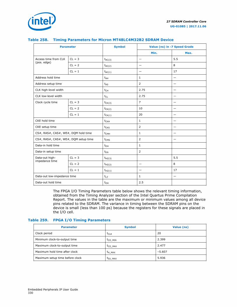
Table 258. Timing Parameters for Micron MT48LC4M32B2 SDRAM Device
Parameter Symbol Value (ns) in -7 Speed Grade
Min. Max.
Access time from CLK(pos. edge)
CL = 3 tAC(3) — 5.5
CL = 2 tAC(2) — 8
CL = 1 tAC(1) — 17
Address hold time tAH 1 —
Address setup time tAS 2 —
CLK high-level width tCH 2.75 —
CLK low-level width tCL 2.75 —
Clock cycle time CL = 3 tCK(3) 7 —
CL = 2 tCK(2) 10 —
CL = 1 tCK(1) 20 —
CKE hold time tCKH 1 —
CKE setup time tCKS 2 —
CS#, RAS#, CAS#, WE#, DQM hold time tCMH 1 —
CS#, RAS#, CAS#, WE#, DQM setup time tCMS 2 —
Data-in hold time tDH 1
Data-in setup time tDS 2
Data-out high-impedance time
CL = 3 tHZ(3) 5.5
CL = 2 tHZ(2) — 8
CL = 1 tHZ(1) — 17
Data-out low-impedance time tLZ 1 —
Data-out hold time tOH 2.5
The FPGA I/O Timing Parameters table below shows the relevant timing information,obtained from the Timing Analyzer section of the Intel Quartus Prime CompilationReport. The values in the table are the maximum or minimum values among all devicepins related to the SDRAM. The variance in timing between the SDRAM pins on thedevice is small (less than 100 ps) because the registers for these signals are placed inthe I/O cell.
Table 259. FPGA I/O Timing Parameters
Parameter Symbol Value (ns)
Clock period tCLK 20
Minimum clock-to-output time tCO_MIN 2.399
Maximum clock-to-output time tCO_MAX 2.477
Maximum hold time after clock tH_MAX –5.607
Maximum setup time before clock tSU_MAX 5.936
27 SDRAM Controller Core
UG-01085 | 2017.11.06
Embedded Peripherals IP User Guide330

You must compile the design in the Intel Quartus Prime software to obtain the I/Otiming information for the design. Although Intel FPGA device family datasheetscontain generic I/O timing information for each device, the Intel Quartus PrimeCompilation Report provides the most precise timing information for your specificdesign.
The timing values found in the compilation report can change, depending on fitting,pin location, and other Intel Quartus Prime logic settings. When you recompile thedesign in the Intel Quartus Prime software, verify that the I/O timing has not changedsignificantly.
The following examples illustrate the calculations from figures Maximum SDRAM ClockLag and Maximum Lead also using the values from the Timing Parameters and FPGAI/O Timing Parameters table.
The SDRAM clock can lag the controller clock by the lesser of Read Lag or Write Lag:
Read Lag = tOH(SDRAM) – tH_MAX(FPGA)
= 2.5 ns – (–5.607 ns) = 8.107 ns
or
Write Lag = tCLK – tCO_MAX(FPGA) – tDS(SDRAM)
= 20 ns – 2.477 ns – 2 ns = 15.523 ns
The SDRAM clock can lead the controller clock by the lesser of Read Lead or WriteLead:
Read Lead = tCO_MIN(FPGA) – tDH(SDRAM)
= 2.399 ns – 1.0 ns = 1.399 ns
or
Write Lead = tCLK – tHZ(3)(SDRAM) – tSU_MAX(FPGA)
= 20 ns – 5.5 ns – 5.936 ns = 8.564 ns
Therefore, for this example you can shift the phase of the SDRAM clock from –8.107 ns to 1.399 ns relative to the controller clock. Choosing a phase shift in themiddle of this window results in the value (–8.107 + 1.399)/2 = –3.35 ns.
27.8 Document Revision History
Table 260. SDRAM Controller Core Revision History
Date Version Changes
May 2016 2016.05.03 Maintenance release.
July 2014 2014.07.24 Removed mention of SOPC Builder, updated to Platform Designer
December 2010 v10.1.0 Removed the “Device Support”, “Instantiating the Core in SOPC Builder”,and “Referenced Documents” sections.
July 2010 v10.0.0 No change from previous release.
continued...
27 SDRAM Controller Core
UG-01085 | 2017.11.06
Embedded Peripherals IP User Guide331

Date Version Changes
November 2009 v9.1.0 No change from previous release.
March 2009 v9.0.0 No change from previous release.
November 2008 v8.1.0 Changed to 8-1/2 x 11 page size. No change to content.
May 2008 v8.0.0 No change from previous release.
For previous versions of this chapter, refer to the Intel Quartus Prime HandbookArchive.
27 SDRAM Controller Core
UG-01085 | 2017.11.06
Embedded Peripherals IP User Guide332

28 Tri-State SDRAM Core
28.1 Core Overview
The Intel SDRAM Tri-State Controller core with Avalon interface provides an AvalonMemory-Mapped (Avalon-MM) interface to off-chip SDRAM. The SDRAM controllerallows designers to create custom systems in an Intel FPGA device that connect easilyto SDRAM chips. The SDRAM controller supports standard SDRAM defined by thePC100 specification.
SDRAM is commonly used in cost-sensitive applications requiring large amounts ofvolatile memory. While SDRAM is relatively inexpensive, control logic is required toperform refresh operations, open-row management, and other delays and commandsequences. The SDRAM controller connects to one or more SDRAM chips, and handlesall SDRAM protocol requirements. The SDRAM controller core presents an Avalon-MMslave port that appears as linear memory (flat address space) to Avalon-MM masterperipherals.
The Avalon-MM interface is latency-aware, allowing read transfers to be pipelined. Thecore can optionally share its address and data buses with other off-chip Avalon-MM tri-state devices. This feature is valuable in systems that have limited I/O pins, yet mustconnect to multiple memory chips in addition to SDRAM.
The Intel SDRAM Tri-State Controller has the same functionality as the SDRAMController Core with the addition of the Tri-State feature.
Related Links
Avalon Interface Specifications
28.2 Feature Description
The Intel SDRAM Tri-State controller core has the following features:
• Maximum frequency of 100-MHz
• Single clock domain design
• Sharing of dq/dqm/addr I/
UG-01085 | 2017.11.06
Intel Corporation. All rights reserved. Intel, the Intel logo, Altera, Arria, Cyclone, Enpirion, MAX, Nios, Quartusand Stratix words and logos are trademarks of Intel Corporation or its subsidiaries in the U.S. and/or othercountries. Intel warrants performance of its FPGA and semiconductor products to current specifications inaccordance with Intel's standard warranty, but reserves the right to make changes to any products and servicesat any time without notice. Intel assumes no responsibility or liability arising out of the application or use of anyinformation, product, or service described herein except as expressly agreed to in writing by Intel. Intelcustomers are advised to obtain the latest version of device specifications before relying on any publishedinformation and before placing orders for products or services.*Other names and brands may be claimed as the property of others.
ISO9001:2008Registered

28.2.1 Block Diagram
Figure 86. Tri-State SDRAM Block Diagram
SDRAMInterface
Tri-stateConduitMaster Signals
altera_sdram_controller
Avalon-MMInterface
Clock Reset
RequestBuffer
Init FSM
Main FSM
Signa
l Gen
erat
ion
28.3 Configuration Parameter
The following table shows the configuration parameters available for user to programduring generation time of the IP core.
28.3.1 Memory Profile Page
The Memory Profile page allows you to specify the structure of the SDRAM subsystemsuch as address and data bus widths, the number of chip select signals, and thenumber of banks.
Table 261. Configuration Parameters
Parameter GUI Legal Values Default Values Units
Data Width 8, 16, 32, 64 32 (Bit)s
Architecture Chip Selects 1, 2, 4, 8 1 (Bit)s
Banks 2, 4 4 (Bit)s
Address Widths Row 11:14 12 (Bit)s
Column 8:14 8 (Bit)s
28.3.2 Timing Page
The Timing page allows designers to enter the timing specifications of the Tri-StateSDRAM chip(s) used. The correct values are available in the manufacturer’s data sheetfor the target SDRAM.
28 Tri-State SDRAM Core
UG-01085 | 2017.11.06
Embedded Peripherals IP User Guide334

Table 262. Configuration Timing Parameters
Parameter GUI Legal Values Default Values Units
CAS latency cycles 1, 2, 3 3 Cycles
Initialization refresh cycles 1:8 2 Cycles
Issue one refresh command every 0.0:156.25 15.625 us
Delay after power up, beforeinitialization
0.0:999.0 100.00 us
Duration of refresh command (t_rfc) 0.0:700.0 70.0 ns
Duration of precharge command (t_rp) 0.0:200.0 20.0 ns
ACTIVE to READ or WRITE delay(t_rcd)
0.0:200.0 20.0 ns
Access time (t_ac) 0.0:999.0 5.5 ns
Write recovery time (t_wr, no autoprecharge)
0.0:140.0 14.0 ns
28.4 Interface
The following are top level signals from core
Table 263. Clock and Reset Signals
Signal Width Direction Description
clk 1 Input System Clock
rst_n 1 Input System asynchronous reset. The signal is assertedasynchronously, but is de-asserted synchronously after therising edge of ssi_clk. The synchronization must beprovided external to this component.
Table 264. Avalon-MM Slave Interface Signals
Signal Width Direction Description
avs_read 1 Input Avalon-MM read control. Asserted to indicate aread transfer. If present, readdata isrequired.
avs_write 1 Input Avalon-MM write control. Asserted to indicatea write transfer. If present, writedata isrequired.
avs_byteenable dqm_width Input Enables specific byte lane(s) during transfer.Each bit corresponds to a byte inavs_writedata and avs_readdata.
avs_address controller_addr_width
Input Avalon-MM address bus.
avs_writedata sdram_data_width Input Avalon-MM write data bus. Driven by the busmaster (bridge unit) during write cycles.
continued...
28 Tri-State SDRAM Core
UG-01085 | 2017.11.06
Embedded Peripherals IP User Guide335

Signal Width Direction Description
avs_readdata sdram_data_width Output Avalon-MM readback data. Driven by thealtera_spi during read cycles.
avs_readdatavalid 1 Output Asserted to indicate that the avs_readdatasignals contains valid data in response to aprevious read request.
avs_waitrequest 1 Output Asserted when it is unable to respond to aread or write request.
Table 265. Tristate Conduit Master / SDRAM Interface Signals
Signal Width Direction Description
tcm_grant 1 Input When asserted, indicatesthat a tristate conduitmaster has been grantedaccess to performtransactions. tcm_grant isasserted in response to thetcm_request signal andremains asserted until 1cycle following thedeassertion of request.Valid only when pin sharingmode is enabled.
tcm_request 1 Output The meaning oftcm_request depends onthe state of the tcm_grantsignal, as the following rulesdictate:• When tcm_request is
asserted and tcm_grantis deasserted,tcm_request isrequesting access for thecurrent cycle.
• When tcm_request isasserted and tcm_grantis asserted,tcm_request isrequesting access for thenext cycle; consequently,tcm_request should bedeasserted on the finalcycle of an access.
Because tcm_request isdeasserted in the last cycleof a bus access, it can bereasserted immediatelyfollowing the final cycle of atransfer, making bothrearbitration and continuousbus access possible if noother masters arerequesting access.Once asserted,tcm_request must remainasserted until granted;consequently, the shortestbus access is 2 cycles.Valid only when pin-sharingmode is enabled.
continued...
28 Tri-State SDRAM Core
UG-01085 | 2017.11.06
Embedded Peripherals IP User Guide336
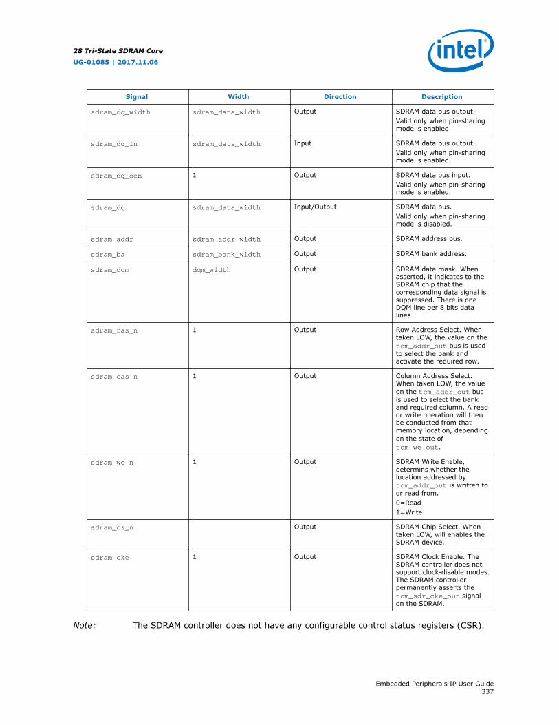
Signal Width Direction Description
sdram_dq_width sdram_data_width Output SDRAM data bus output.Valid only when pin-sharingmode is enabled
sdram_dq_in sdram_data_width Input SDRAM data bus output.Valid only when pin-sharingmode is enabled.
sdram_dq_oen 1 Output SDRAM data bus input.Valid only when pin-sharingmode is enabled.
sdram_dq sdram_data_width Input/Output SDRAM data bus.Valid only when pin-sharingmode is disabled.
sdram_addr sdram_addr_width Output SDRAM address bus.
sdram_ba sdram_bank_width Output SDRAM bank address.
sdram_dqm dqm_width Output SDRAM data mask. Whenasserted, it indicates to theSDRAM chip that thecorresponding data signal issuppressed. There is oneDQM line per 8 bits datalines
sdram_ras_n 1 Output Row Address Select. Whentaken LOW, the value on thetcm_addr_out bus is usedto select the bank andactivate the required row.
sdram_cas_n 1 Output Column Address Select.When taken LOW, the valueon the tcm_addr_out busis used to select the bankand required column. A reador write operation will thenbe conducted from thatmemory location, dependingon the state oftcm_we_out.
sdram_we_n 1 Output SDRAM Write Enable,determins whether thelocation addressed bytcm_addr_out is written toor read from.0=Read1=Write
sdram_cs_n Output SDRAM Chip Select. Whentaken LOW, will enables theSDRAM device.
sdram_cke 1 Output SDRAM Clock Enable. TheSDRAM controller does notsupport clock-disable modes.The SDRAM controllerpermanently asserts thetcm_sdr_cke_out signalon the SDRAM.
Note: The SDRAM controller does not have any configurable control status registers (CSR).
28 Tri-State SDRAM Core
UG-01085 | 2017.11.06
Embedded Peripherals IP User Guide337

28.5 Reset and Clock Requirements
The main reset input signal to the SDRAM is treated as an asynchronous reset inputfrom the SDRAM core perspective. A reset synchronizer circuit, as typicallyimplemented for each reset domain in a complete SOC/ASIC system is notimplemented within the SDRAM core. Instead, this reset synchronizer circuit should beimplemented externally to the SDRAM, in a higher hierarchy within the completesystem design, so that the “asynchronous assertion, synchronous de-assertion” rule isfulfilled.
The SDRAM core accepts an input clock at its clk input with maximum frequency of100-MHz. The other requirements for the clock, such as its minimum frequency shouldbe similar to the requirement of the external SDRAM which the SDRAM is interfacedto.
28.6 Architecture
The SDRAM Controller connects to one or more SDRAM chips, and handles all SDRAMprotocol requirements. Internal to the device, the core presents an Avalon-MM slaveports that appears as a linear memory (flat address space) to Avalon-MM masterdevice.
The core can access SDRAM subsystems with:
• Various data widths (8-, 16-, 32- or 64-bits)
• Various memory sizes
• Multiple chip selects
The Avalon-MM interface is latency-aware, allowing read transfers to be pipelined. Thecore can optionally share its address and data buses with other off-chip Avalon-MM tri-state devices.
Note: Limitations: for now the arbitration control of this mode should be handled by thehost/master in the system to avoid a device monopolizing the shared buses.
Control logic within the SDRAM core responsible for the main functionality listedbelow, among others:
• Refresh operation
• Open_row management
• Delay and command management
Use of the data bus is intricate and thus requires a complex DRAM controller circuit.This is because data written to the DRAM must be presented in the same cycle as thewrite command, but reads produce output 2 or 3 cycles after the read command. TheSDRAM controller must ensure that the data bus is never required for a read and awrite at the same time.
28.6.1 Avalon-MM Slave Interface and CSR
The host processor perform data read and write operation to the external SDRAMdevices through the Avalon-MM interface of the SDRAM core.
28 Tri-State SDRAM Core
UG-01085 | 2017.11.06
Embedded Peripherals IP User Guide338

Please refer to Avalon Interface Specifications for more information on the details ofthe Avalon-MM Slave Interface.
Related Links
Avalon Interface Specifications
28.6.2 Block Level Usage Model
Figure 87. Shared-Bus System
28.7 Document Revision History
Table 266. Intel SDRAM Tri-State Controller Core Revision History
Date Version Changes
July 2014 2014.07.24 Initial release.
28 Tri-State SDRAM Core
UG-01085 | 2017.11.06
Embedded Peripherals IP User Guide339
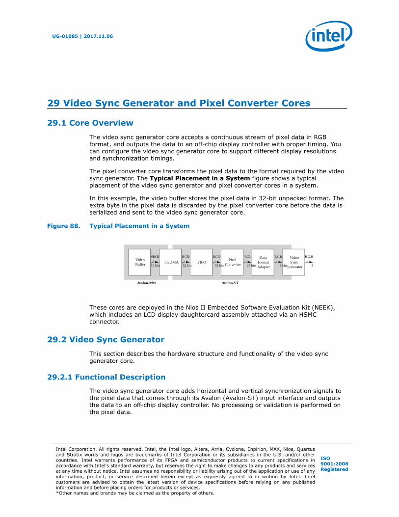
29 Video Sync Generator and Pixel Converter Cores
29.1 Core Overview
The video sync generator core accepts a continuous stream of pixel data in RGBformat, and outputs the data to an off-chip display controller with proper timing. Youcan configure the video sync generator core to support different display resolutionsand synchronization timings.
The pixel converter core transforms the pixel data to the format required by the videosync generator. The Typical Placement in a System figure shows a typicalplacement of the video sync generator and pixel converter cores in a system.
In this example, the video buffer stores the pixel data in 32-bit unpacked format. Theextra byte in the pixel data is discarded by the pixel converter core before the data isserialized and sent to the video sync generator core.
Figure 88. Typical Placement in a System
VideoBuffer
SGDMA FIFOPixel
Converter
DataFormatAdapter
VideoSync
Generator32 bits 32 bits 32 bits 24 bits 8 bits 8 bits
0RGB BGR0 BGR0 BGR B,G,R B,G,R
TS-nolavAMM-nolavA
VideoBuffer
SGDMA FIFOPixel
Converter
DataFormatAdapter
VideoSync
Generator32 bits 32 bits 32 bits 24 bits 8 bits 8 bits
0RGB BGR0 BGR0 BGR B,G,R B,G,R
TS-nolavAMM-nolavA
These cores are deployed in the Nios II Embedded Software Evaluation Kit (NEEK),which includes an LCD display daughtercard assembly attached via an HSMCconnector.
29.2 Video Sync Generator
This section describes the hardware structure and functionality of the video syncgenerator core.
29.2.1 Functional Description
The video sync generator core adds horizontal and vertical synchronization signals tothe pixel data that comes through its Avalon (Avalon-ST) input interface and outputsthe data to an off-chip display controller. No processing or validation is performed onthe pixel data.
UG-01085 | 2017.11.06
Intel Corporation. All rights reserved. Intel, the Intel logo, Altera, Arria, Cyclone, Enpirion, MAX, Nios, Quartusand Stratix words and logos are trademarks of Intel Corporation or its subsidiaries in the U.S. and/or othercountries. Intel warrants performance of its FPGA and semiconductor products to current specifications inaccordance with Intel's standard warranty, but reserves the right to make changes to any products and servicesat any time without notice. Intel assumes no responsibility or liability arising out of the application or use of anyinformation, product, or service described herein except as expressly agreed to in writing by Intel. Intelcustomers are advised to obtain the latest version of device specifications before relying on any publishedinformation and before placing orders for products or services.*Other names and brands may be claimed as the property of others.
ISO9001:2008Registered
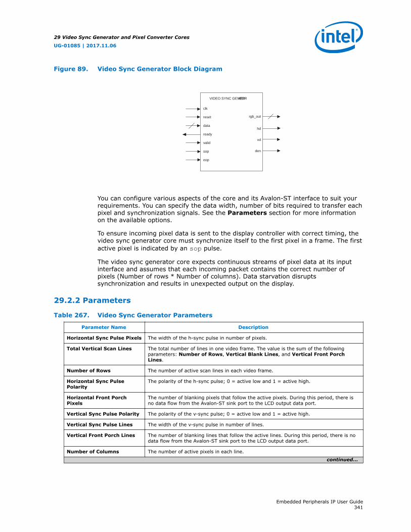
Figure 89. Video Sync Generator Block Diagram
clk
reset
data
ready
valid
sop
eop
rgb_out
hd
vd
den
VIDEO SYNC GENERATOR
You can configure various aspects of the core and its Avalon-ST interface to suit yourrequirements. You can specify the data width, number of bits required to transfer eachpixel and synchronization signals. See the Parameters section for more informationon the available options.
To ensure incoming pixel data is sent to the display controller with correct timing, thevideo sync generator core must synchronize itself to the first pixel in a frame. The firstactive pixel is indicated by an sop pulse.
The video sync generator core expects continuous streams of pixel data at its inputinterface and assumes that each incoming packet contains the correct number ofpixels (Number of rows * Number of columns). Data starvation disruptssynchronization and results in unexpected output on the display.
29.2.2 Parameters
Table 267. Video Sync Generator Parameters
Parameter Name Description
Horizontal Sync Pulse Pixels The width of the h-sync pulse in number of pixels.
Total Vertical Scan Lines The total number of lines in one video frame. The value is the sum of the followingparameters: Number of Rows, Vertical Blank Lines, and Vertical Front PorchLines.
Number of Rows The number of active scan lines in each video frame.
Horizontal Sync PulsePolarity
The polarity of the h-sync pulse; 0 = active low and 1 = active high.
Horizontal Front PorchPixels
The number of blanking pixels that follow the active pixels. During this period, there isno data flow from the Avalon-ST sink port to the LCD output data port.
Vertical Sync Pulse Polarity The polarity of the v-sync pulse; 0 = active low and 1 = active high.
Vertical Sync Pulse Lines The width of the v-sync pulse in number of lines.
Vertical Front Porch Lines The number of blanking lines that follow the active lines. During this period, there is nodata flow from the Avalon-ST sink port to the LCD output data port.
Number of Columns The number of active pixels in each line.
continued...
29 Video Sync Generator and Pixel Converter Cores
UG-01085 | 2017.11.06
Embedded Peripherals IP User Guide341
Parameter Name Description
Horizontal Blank Pixels The number of blanking pixels that precede the active pixels. During this period, there isno data flow from the Avalon-ST sink port to the LCD output data port.
Total Horizontal Scan Pixels The total number of pixels in one line. The value is the sum of the following parameters:Number of Columns, Horizontal Blank Pixel, and Horizontal Front Porch Pixels.
bits Per Pixel The number of bits required to transfer one pixel. Valid values are 1 and 3. Thisparameter, when multiplied by Data Stream Bit Width must be equal to the totalnumber of bits in one pixel. This parameter affects the operating clock frequency, asshown in the following equation:Operating clock frequency = (bits per pixel) * (Pixel_rate), where Pixel_rate (in MHz) = ((Total Horizontal Scan Pixels) * (Total Vertical Scan Lines)* (Display refresh rate in Hz))/1000000.
Vertical Blank Lines The number of blanking lines that proceed the active lines. During this period, there isno data flow from the Avalon-ST sink port to the LCD output data port.
Data Stream Bit Width The width of the inbound and outbound data.
29.2.3 Signals
Table 268. Video Sync Generator Core Signals
Signal Name Width (Bits) Direction Description
Global Signals
clk 1 Input System clock.
reset 1 Input System reset.
Avalon-ST Signals
data Variable-width Input Incoming pixel data. The datawidth is determined by the parameterData Stream Bit Width.
ready 1 Output This signal is asserted when the video sync generator is ready toreceive the pixel data.
valid 1 Input This signal is not used by the video sync generator core because thecore always expects valid pixel data on the next clock cycle after theready signal is asserted.
sop 1 Input Start-of-packet. This signal is asserted when the first pixel is received.
eop 1 Input End-of-packet. This signal is asserted when the last pixel is received.
LCD Output Signals
rgb_out Variable-width Output Display data. The datawidth is determined by the parameter DataStream Bit Width.
hd 1 Output Horizontal synchronization pulse for display.
vd 1 Output Vertical synchronization pulse for display.
den 1 Output This signal is asserted when the video sync generator core outputsvalid data for display.
29.2.4 Timing Diagrams
The horizontal and vertical synchronization timings are determined by the parameterssetting. The table below shows the horizontal synchronization timing when theparameters Data Stream Bit Width and bits Per Pixel are set to 8 and 3,respectively.
29 Video Sync Generator and Pixel Converter Cores
UG-01085 | 2017.11.06
Embedded Peripherals IP User Guide342

Figure 90. Horizontal Synchronization Timing—8 Bits DataWidth and 3 bits Per Pixel
clk
hd
den
rgb_out R G B R G B
Horizontal sync pulse
Horizontal front porch
1 pixel
Horizontal blank pixels
Horizontal synchronization width
The table below sho.ws the horizontal synchronization timing when the parametersData Stream Bit Width and bits Per Pixel are set to 24 and 1, respectively.
Figure 91. Horizontal Synchronization Timing—24 Bits DataWidth and 1 Beat Per Pixel
clk
hd
den
rgb_out RGB
Horizontal synchronization pulse
Horizontal blank pixels Horizontal front porch
1 pixel
RGBRGB RGBRGBRGB
Horizontal synchronization width
Figure 92. Vertical Synchronization Timing—8 Bits DataWidth and 3 bits Per Pixel / 24Bits DataWidth and 1 Beat Per Pixel
hd
den
Vertical blank lines
Horizontal synchronization width
vd
Vertical synchronization width
Vertical front porch
Vertical synchronization pulse
29.3 Pixel Converter
This section describes the hardware structure and functionality of the pixel convertercore.
29.3.1 Functional Description
The pixel converter core receives pixel data on its Avalon-ST input interface andtransforms the pixel data to the format required by the video sync generator. The leastsignificant byte of the 32-bit wide pixel data is removed and the remaining 24 bits arewired directly to the core's Avalon-ST output interface.
29 Video Sync Generator and Pixel Converter Cores
UG-01085 | 2017.11.06
Embedded Peripherals IP User Guide343
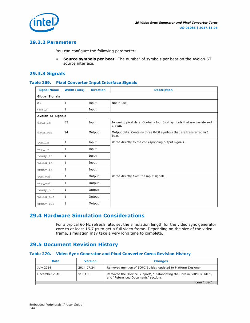
29.3.2 Parameters
You can configure the following parameter:
• Source symbols per beat—The number of symbols per beat on the Avalon-STsource interface.
29.3.3 Signals
Table 269. Pixel Converter Input Interface Signals
Signal Name Width (Bits) Direction Description
Global Signals
clk 1 Input Not in use.
reset_n 1 Input
Avalon-ST Signals
data_in 32 Input Incoming pixel data. Contains four 8-bit symbols that are transferred in1 beat.
data_out 24 Output Output data. Contains three 8-bit symbols that are transferred in 1beat.
sop_in 1 Input Wired directly to the corresponding output signals.
eop_in 1 Input
ready_in 1 Input
valid_in 1 Input
empty_in 1 Input
sop_out 1 Output Wired directly from the input signals.
eop_out 1 Output
ready_out 1 Output
valid_out 1 Output
empty_out 1 Output
29.4 Hardware Simulation Considerations
For a typical 60 Hz refresh rate, set the simulation length for the video sync generatorcore to at least 16.7 μs to get a full video frame. Depending on the size of the videoframe, simulation may take a very long time to complete.
29.5 Document Revision History
Table 270. Video Sync Generator and Pixel Converter Cores Revision History
Date Version Changes
July 2014 2014.07.24 Removed mention of SOPC Builder, updated to Platform Designer
December 2010 v10.1.0 Removed the “Device Support”, “Instantiating the Core in SOPC Builder”,and “Referenced Documents” sections.
continued...
29 Video Sync Generator and Pixel Converter Cores
UG-01085 | 2017.11.06
Embedded Peripherals IP User Guide344
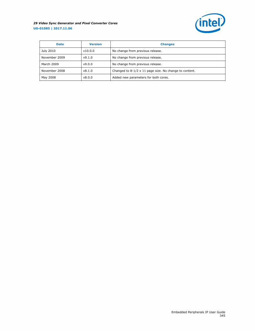
Date Version Changes
July 2010 v10.0.0 No change from previous release.
November 2009 v9.1.0 No change from previous release.
March 2009 v9.0.0 No change from previous release.
November 2008 v8.1.0 Changed to 8-1/2 x 11 page size. No change to content.
May 2008 v8.0.0 Added new parameters for both cores.
29 Video Sync Generator and Pixel Converter Cores
UG-01085 | 2017.11.06
Embedded Peripherals IP User Guide345

30 Intel FPGA Interrupt Latency Counter Core
30.1 Core Overview
A processor running a program can be instructed to divert from its original executionpath by an interrupt signal generated either by peripheral hardware or the firmwarethat is currently being executed. The processor now executes the portions of theprogram code that handles the interrupt requests known as Interrupt Service Routines(ISR) by moving to the instruction pointer to the ISR, and then continues operation.Upon completion of the routine, the processor returns to the previous location.
Intel FPGA's Interrupt Latency Calculator (ILC) is developed in mind to measure thetime taken in terms of clock cycles to complete the interrupt service routine. Dataobtained from the ILC is utilized by other latency sensitive IPs in order for it tomaintain its proper operation. The data from the ILC can also be used to help thegeneral firmware debugging exercise.
The ILC sits as a parallel to any interrupt receiver that will consume and perform aninterrupt service routine. The following figure shows the orientation of a ILC in asystem design.
Figure 93. Usage model of Interrupt Latency Calculator
Processor Interrupt Latency Calculator
Peripheral
DataMaster
IRQ Receiver
CSRSlave
IRQ Receiver
IRQ Sender
30.2 Feature Description
The ILC is made up of three sub functional blocks. The top level interface is AvalonMemory Mapped (Avalon-MM) protocol compliant. The interrupt detector block will beactivated by the rising edge of the interrupt signal or pulse, determined by aparameter during component generation. The interrupt detector block determines
UG-01085 | 2017.11.06
Intel Corporation. All rights reserved. Intel, the Intel logo, Altera, Arria, Cyclone, Enpirion, MAX, Nios, Quartusand Stratix words and logos are trademarks of Intel Corporation or its subsidiaries in the U.S. and/or othercountries. Intel warrants performance of its FPGA and semiconductor products to current specifications inaccordance with Intel's standard warranty, but reserves the right to make changes to any products and servicesat any time without notice. Intel assumes no responsibility or liability arising out of the application or use of anyinformation, product, or service described herein except as expressly agreed to in writing by Intel. Intelcustomers are advised to obtain the latest version of device specifications before relying on any publishedinformation and before placing orders for products or services.*Other names and brands may be claimed as the property of others.
ISO9001:2008Registered
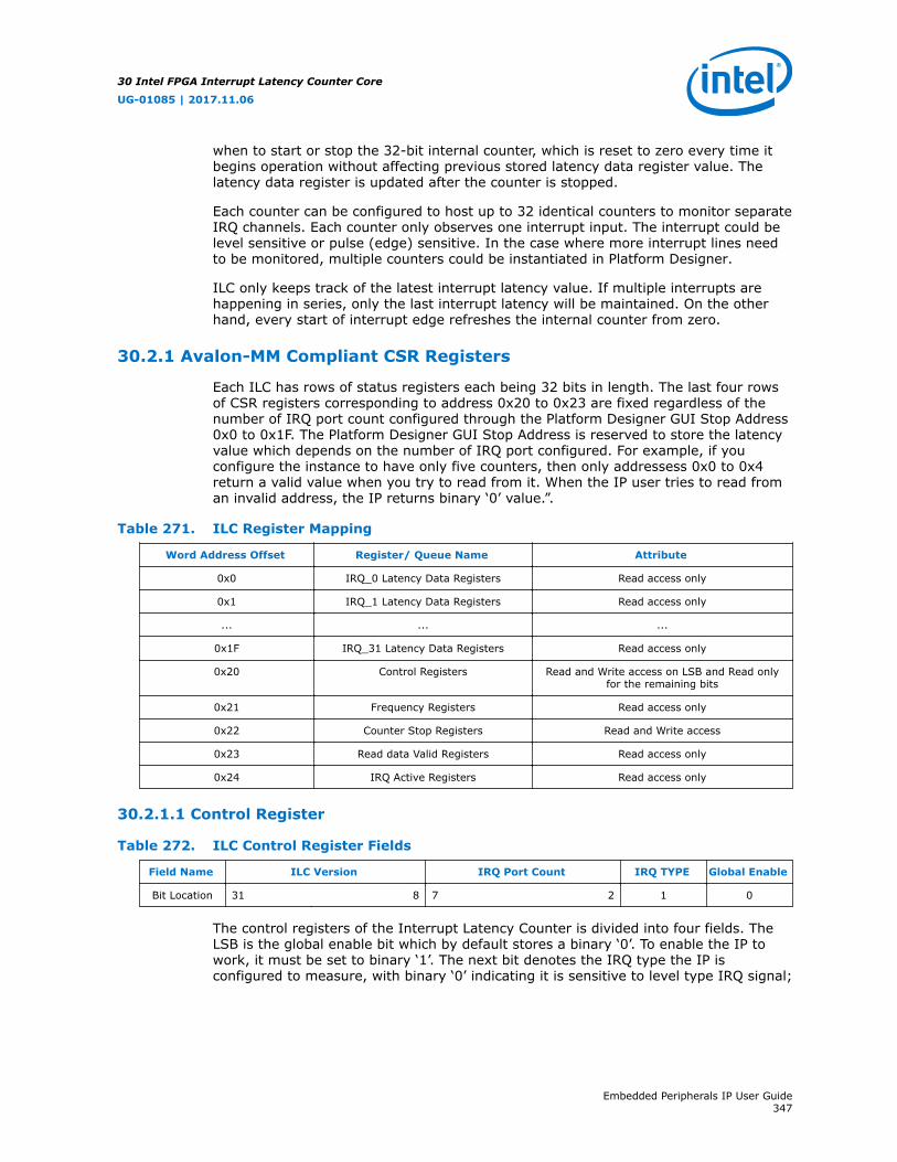
when to start or stop the 32-bit internal counter, which is reset to zero every time itbegins operation without affecting previous stored latency data register value. Thelatency data register is updated after the counter is stopped.
Each counter can be configured to host up to 32 identical counters to monitor separateIRQ channels. Each counter only observes one interrupt input. The interrupt could belevel sensitive or pulse (edge) sensitive. In the case where more interrupt lines needto be monitored, multiple counters could be instantiated in Platform Designer.
ILC only keeps track of the latest interrupt latency value. If multiple interrupts arehappening in series, only the last interrupt latency will be maintained. On the otherhand, every start of interrupt edge refreshes the internal counter from zero.
30.2.1 Avalon-MM Compliant CSR Registers
Each ILC has rows of status registers each being 32 bits in length. The last four rowsof CSR registers corresponding to address 0x20 to 0x23 are fixed regardless of thenumber of IRQ port count configured through the Platform Designer GUI Stop Address0x0 to 0x1F. The Platform Designer GUI Stop Address is reserved to store the latencyvalue which depends on the number of IRQ port configured. For example, if youconfigure the instance to have only five counters, then only addressess 0x0 to 0x4return a valid value when you try to read from it. When the IP user tries to read froman invalid address, the IP returns binary ‘0’ value.”.
Table 271. ILC Register Mapping
Word Address Offset Register/ Queue Name Attribute
0x0 IRQ_0 Latency Data Registers Read access only
0x1 IRQ_1 Latency Data Registers Read access only
... ... ...
0x1F IRQ_31 Latency Data Registers Read access only
0x20 Control Registers Read and Write access on LSB and Read onlyfor the remaining bits
0x21 Frequency Registers Read access only
0x22 Counter Stop Registers Read and Write access
0x23 Read data Valid Registers Read access only
0x24 IRQ Active Registers Read access only
30.2.1.1 Control Register
Table 272. ILC Control Register Fields
Field Name ILC Version IRQ Port Count IRQ TYPE Global Enable
Bit Location 31 8 7 2 1 0
The control registers of the Interrupt Latency Counter is divided into four fields. TheLSB is the global enable bit which by default stores a binary ‘0’. To enable the IP towork, it must be set to binary ‘1’. The next bit denotes the IRQ type the IP isconfigured to measure, with binary ‘0’ indicating it is sensitive to level type IRQ signal;
30 Intel FPGA Interrupt Latency Counter Core
UG-01085 | 2017.11.06
Embedded Peripherals IP User Guide347
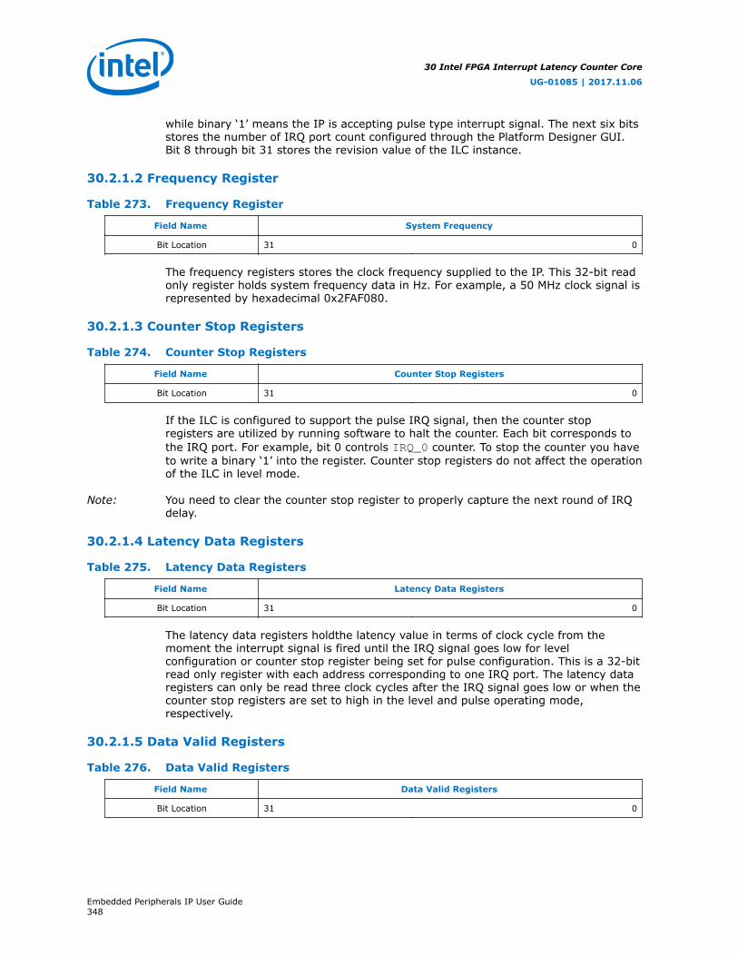
while binary ‘1’ means the IP is accepting pulse type interrupt signal. The next six bitsstores the number of IRQ port count configured through the Platform Designer GUI.Bit 8 through bit 31 stores the revision value of the ILC instance.
30.2.1.2 Frequency Register
Table 273. Frequency Register
Field Name System Frequency
Bit Location 31 0
The frequency registers stores the clock frequency supplied to the IP. This 32-bit readonly register holds system frequency data in Hz. For example, a 50 MHz clock signal isrepresented by hexadecimal 0x2FAF080.
30.2.1.3 Counter Stop Registers
Table 274. Counter Stop Registers
Field Name Counter Stop Registers
Bit Location 31 0
If the ILC is configured to support the pulse IRQ signal, then the counter stopregisters are utilized by running software to halt the counter. Each bit corresponds tothe IRQ port. For example, bit 0 controls IRQ_0 counter. To stop the counter you haveto write a binary ‘1’ into the register. Counter stop registers do not affect the operationof the ILC in level mode.
Note: You need to clear the counter stop register to properly capture the next round of IRQdelay.
30.2.1.4 Latency Data Registers
Table 275. Latency Data Registers
Field Name Latency Data Registers
Bit Location 31 0
The latency data registers holdthe latency value in terms of clock cycle from themoment the interrupt signal is fired until the IRQ signal goes low for levelconfiguration or counter stop register being set for pulse configuration. This is a 32-bitread only register with each address corresponding to one IRQ port. The latency dataregisters can only be read three clock cycles after the IRQ signal goes low or when thecounter stop registers are set to high in the level and pulse operating mode,respectively.
30.2.1.5 Data Valid Registers
Table 276. Data Valid Registers
Field Name Data Valid Registers
Bit Location 31 0
30 Intel FPGA Interrupt Latency Counter Core
UG-01085 | 2017.11.06
Embedded Peripherals IP User Guide348

The data valid registers indicate whether the data from the latency data regsters areready to be read or not. By default, these registers hold a binary value of ‘0’ out ofreset. Once the counter data is transfered to the latency data register, thecorresponding bit within the data valid register is set to binary '1'. It reverts back tobinary ‘0’ after a read operation has been consumed by the ILC.
30.2.2 32-bit Counter
The 32-bit positive edge triggered D-flop base up counter takes in a reset signal whichclears all the registers to zero. It also has an enable signal that determines when thecounter operation is turned on or off.
30.2.3 Interrupt Detector
The interrupt detector can be customized to detect either signal edges or pulse usingthe Platform Designer interface. The interrupt detector generates an enable signal tostart and stop the 32-bit counter.
30.3 Component Interface
Intel FPGA Interrupt Latency Calculator has an Avalon-MM slave interface whichcommunicates with the Interrupt service routine initiator.
The table below shows the component interface that is available on the Intel FPGAInterrupt Latency Counter IP.
Table 277. Available Component Interfaces
Interface Port Description Remarks
Avalon-MM Slave (address , write,waitrequest , writedata[31:0], read,readdata[31:0])
Avalon-MM Slave interface forprocessor to talk to the IP.
This Avalon-MM slave interfaceobserves zero cycles read latency withwaitrequest signal. The waitrequestsignal defaults to binary ‘1’ if there isno ongoing operation. If the Avalon-MM Read or Write signal goes high, thewaitrequest signal only goes low if thereaddata_valid_register goes high.
Clock Clock input of component. Clock signal to feed the latecy counterlogics.
Reset_n Active LOW reset input/s. Support asynchronous reset assertion.De-assertion of reset has to besynchronized to the input clock.
IRQ IRQ signal from the interrupt signalinitiator
Interrupt assertion and deassertion issynchronized to input clock.
30.4 Component Parameterization
The table below shows the configuration parameters available on the Intel FPGAInterrupt Latency Counter IP.
30 Intel FPGA Interrupt Latency Counter Core
UG-01085 | 2017.11.06
Embedded Peripherals IP User Guide349
Table 278. Available Component Parameterizations
Parameter Name Description Default Value Allowable Range
INTERRUPT_TYPE Value 0: level sensitiveinterrupt inputValue 1: edge/pulseinterrupt input
0 0,1
CLOCK_RATE Frequency of the clock signalthat is connected to the IP
0 0 – 2^32
IRQ_PORT_COUNT Configure number of IRQPORT to use
32 1 - 32
30.5 Software Access
Since the component supports two types of incoming interrupts - level and edge/pulse, the software access routine for supporting each of the interrupt types hasslightly different expectations.
30.5.1 Routine for Level Sensitive Interrupts
The software access routine for level sensitive interrupts is as follows:
1. Upon completion of ISR, read the data valid bit to ensure that the data is "valid"before reading the interrupt latency counter.
2. Read from the Latency Data Register to obtain the actual cycle spend for theinterrupt.The value presented is in the amount of clock cycle associated with the clockconnected to Interrupt Latency Counter.
30.5.2 Routine for Edge/Pulse Sensitive Interrupts
The software access routine for edge/pulse sensitive interrupts is as follows:
1. Upon completion of ISR, or at the end of ISR, software needs to write binary ‘1’ toone of the 32-bit registers of the Counter Stop Register to stop the internalcounter from counting. The LSB represents counter 0 and the MSB representscounter 31. This is the same as the level sensitive interrupt. Data valid bit isrecommended to be read before reading the latency counter.
2. Read from Latency Data Register to obtain the actual cycle spend for the interrupt.The counter stop bit only needs clearing when the IP is configured to accept pulseIRQ. If level IRQ is employed. The counter stop bit is ignored.
30 Intel FPGA Interrupt Latency Counter Core
UG-01085 | 2017.11.06
Embedded Peripherals IP User Guide350
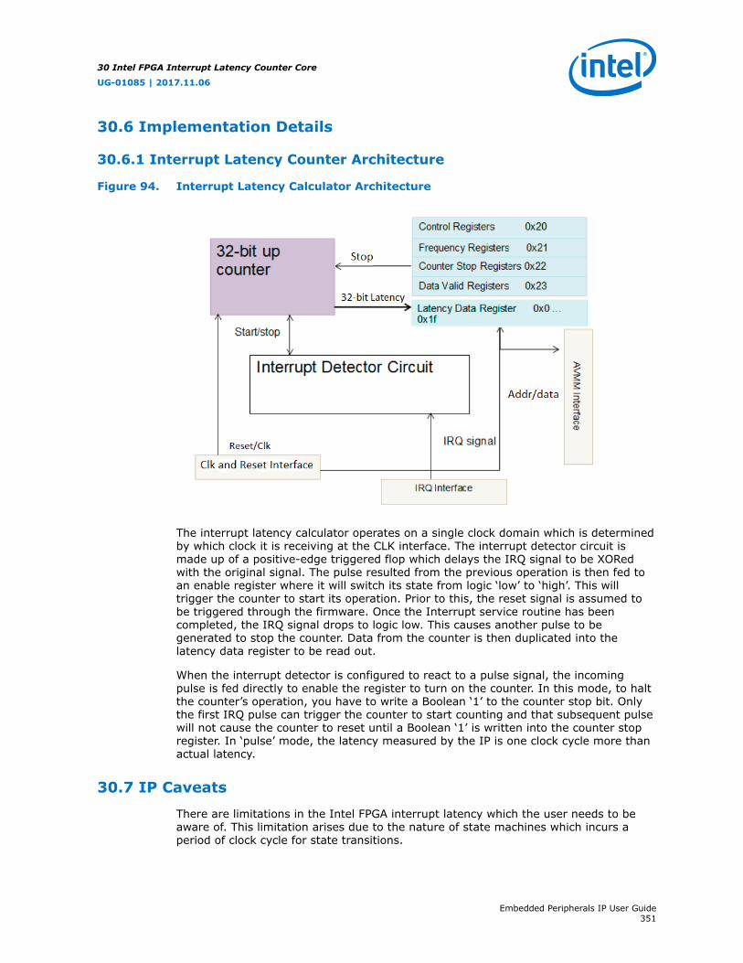
30.6 Implementation Details
30.6.1 Interrupt Latency Counter Architecture
Figure 94. Interrupt Latency Calculator Architecture
The interrupt latency calculator operates on a single clock domain which is determinedby which clock it is receiving at the CLK interface. The interrupt detector circuit ismade up of a positive-edge triggered flop which delays the IRQ signal to be XORedwith the original signal. The pulse resulted from the previous operation is then fed toan enable register where it will switch its state from logic ‘low’ to ‘high’. This willtrigger the counter to start its operation. Prior to this, the reset signal is assumed tobe triggered through the firmware. Once the Interrupt service routine has beencompleted, the IRQ signal drops to logic low. This causes another pulse to begenerated to stop the counter. Data from the counter is then duplicated into thelatency data register to be read out.
When the interrupt detector is configured to react to a pulse signal, the incomingpulse is fed directly to enable the register to turn on the counter. In this mode, to haltthe counter’s operation, you have to write a Boolean ‘1’ to the counter stop bit. Onlythe first IRQ pulse can trigger the counter to start counting and that subsequent pulsewill not cause the counter to reset until a Boolean ‘1’ is written into the counter stopregister. In ‘pulse’ mode, the latency measured by the IP is one clock cycle more thanactual latency.
30.7 IP Caveats
There are limitations in the Intel FPGA interrupt latency which the user needs to beaware of. This limitation arises due to the nature of state machines which incurs aperiod of clock cycle for state transitions.
30 Intel FPGA Interrupt Latency Counter Core
UG-01085 | 2017.11.06
Embedded Peripherals IP User Guide351

1. The data latency registers cannot be read before a first IRQ is fired in any of the32 channels. This causes the Waitrequest signal to be perpetually high whichwould lead to a system stall.
2. The data registers can only be read three clock cycles after the counter registersstop counting. These three clock cycles originate from the state machine movingfrom the start state to the stop/store state. It takes an additional clock cycle topropagate the data from the counter registers to the data store registers.
3. In the pulse IRQ mode, there is an idle cycle present between two consecutivewrite commands into the counter stop register. So, in the event that channel 1 ishalted immediately after channel 0 is halted, then the minimum difference you seein the registered values is 2.
4. The interrupt latency counter will not notify you if an overflow occurs but thecounter can count up to very huge numbers before an overflow happens. Themagnitude of the delay numbers reported will suggest that the system has hungindefinitely.
30.8 Document Revision History
Table 279. Altera Interrupt Latency Counter Core Revision History
Date Version Changes
June 2016 2016.06.17 Updated:• Table 271 on page 347 Added word address offset 0x24• Data Valid Registers on page 348 Updated description• Table 278 on page 350 Parameter name change• IP Caveats on page 351 Added limitation 4
July 2014 2014.07.24 Initial Release
30 Intel FPGA Interrupt Latency Counter Core
UG-01085 | 2017.11.06
Embedded Peripherals IP User Guide352

31 Performance Counter Unit Core
31.1 Core Overview
The performance counter core with Avalon interface enables relatively unobtrusive,real-time profiling of software programs. With the performance counter, you canaccurately measure execution time taken by multiple sections of code. You need onlyadd a single instruction at the beginning and end of each section to be measured.
The main benefit of using the performance counter core is the accuracy of the profilingresults. Alternatives include the following approaches:
• GNU profiler, gprof—gprof provides broad low-precision timing informationabout the entire software system. It uses a substantial amount of RAM, anddegrades the real-time performance. For many embedded applications, gprofdistorts real-time behavior too much to be useful.
• Interval timer peripheral—The interval timer is less intrusive than gprof. It canprovide good results for narrowly targeted sections of code.
The performance counter core is unobtrusive, requiring only a single instruction tostart and stop profiling, and no RAM. It is appropriate for high-precisionmeasurements of narrowly targeted sections of code.
For further discussion of all three profiling methods, refer to AN 391: ProfilingNios II Systems.
The core is designed for use in Avalon-based processor systems, such as a Nios IIprocessor system. Intel FPGA device drivers enable the Nios II processor to usethe performance counters.
31.2 Functional Description
The performance counter core is a set of counters which track clock cycles, timingmultiple sections of your software. You can start and stop these counters in yoursoftware, individually or as a group. You can read cycle counts from hardwareregisters.
The core contains two counters for every section:
• Time: A 64-bit clock cycle counter.
• Events: A 32-bit event counter.
31.2.1 Section Counters
Each 64-bit time counter records the aggregate number of clock cycles spent in asection of code. The 32-bit event counter records the number of times the sectionexecutes.
UG-01085 | 2017.11.06
Intel Corporation. All rights reserved. Intel, the Intel logo, Altera, Arria, Cyclone, Enpirion, MAX, Nios, Quartusand Stratix words and logos are trademarks of Intel Corporation or its subsidiaries in the U.S. and/or othercountries. Intel warrants performance of its FPGA and semiconductor products to current specifications inaccordance with Intel's standard warranty, but reserves the right to make changes to any products and servicesat any time without notice. Intel assumes no responsibility or liability arising out of the application or use of anyinformation, product, or service described herein except as expressly agreed to in writing by Intel. Intelcustomers are advised to obtain the latest version of device specifications before relying on any publishedinformation and before placing orders for products or services.*Other names and brands may be claimed as the property of others.
ISO9001:2008Registered
The performance counter core can have up to seven section counters.
31.2.2 Global Counter
The global counter controls all section counters. The section counters are enabled onlywhen the global counter is running.
The 64-bit global clock cycle counter tracks the aggregate time for which the counterswere enabled. The 32-bit global event counter tracks the number of global events,that is, the number of times the performance counter core has been enabled.
31.2.3 Register Map
The performance counter core has an Avalon Memory-Mapped (Avalon-MM) slaveinterface that provides access to memory-mapped registers. Reading from theregisters retrieves the current times and event counts. Writing to the registers starts,stops, and resets the counters.
Table 280. Performance Counter Core Register Map
Offset Register Name Bit Description
Read Write
31 ... 0 31 ... 1 0
0 T[0]lo global clock cycle counter [31: 0] (1) 0 = STOP1 = RESET
1 T[0]hi global clock cycle counter [63:32] (1) 0 = START
2 Ev[0] global event counter (1) (1)
3 — (1) (1) (1)
4 T[1]lo section 1 clock cycle counter [31:0] (1) 1 = STOP
5 T[1]hi section 1 clock cycle counter [63:32] (1) 0 = START
6 Ev[1] section 1 event counter (1) (1)
7 — (1) (1) (1)
8 T[2]lo section 2 clock cycle counter [31:0] (1) 1 = STOP
9 T[2]hi section 2 clock cycle counter [63:32] (1) 0 = START
10 Ev[2] section 2 event counter (1) (1)
11 — (1) (1) (1)
.
.
.
.
.
.
.
.
.
.
.
.
.
.
.
4n + 0 T[n]lo section n clock cycle counter [31:0] (1) 1 = STOP
4n + 1 T[n]hi section n clock cycle counter [63:32] (1) 0 = START
4n + 2 Ev[n] section n event counter (1) (1)
4n + 3 — (1) (1) (1)
Note :1. Reserved. Read values are undefined. When writing, set reserved bits to zero.
31 Performance Counter Unit Core
UG-01085 | 2017.11.06
Embedded Peripherals IP User Guide354

31.2.4 System Reset
After a system reset, the performance counter core is stopped and disabled, and allcounters are set to zero.
31.3 Configuration
The following sections list the available options in the MegaWizard™ interface.
31.3.1 Define Counters
Choose the number of section counters you want to generate by selecting from theNumber of simultaneously-measured sections list. The performance counter coremay have up to seven sections. If you require more that seven sections, you caninstantiate multiple performance counter cores.
31.3.2 Multiple Clock Domain Considerations
If your Platform Designer system uses multiple clocks, place the performance countercore in the same clock domain as the CPU. Otherwise, it is not possible to convertcycle counts to seconds correctly.
31.4 Hardware Simulation Considerations
You can use this core in simulation with no special considerations.
31.5 Software Programming Model
The following sections describe the software programming model for the performancecounter core.
31.5.1 Software Files
Intel provides the following software files for Nios II systems. These files define thelow-level access to the hardware and provide control and reporting functions. Do notmodify these files.
• altera_avalon_performance_counter.h,altera_avalon_performance_counter.c—The header and source code forthe functions and macros needed to control the performance counter core andretrieve raw results.
• perf_print_formatted_report.c—The source code for simple profilereporting.
31.5.2 Using the Performance Counter
In a Nios II system, you can control the performance counter core with a set of highlyefficient C macros, and extract the results with C functions.
API Summary
31 Performance Counter Unit Core
UG-01085 | 2017.11.06
Embedded Peripherals IP User Guide355

The NNios II application program interface (API) for the performance counter coreconsists of functions, macros and constants.
Table 281. Performance Counter Macros and Functions
Name Summary
PERF_RESET() Stops and disables all counters, resetting them to 0.
PERF_START_MEASURING() Starts the global counter and enables section counters.
PERF_STOP_MEASURING() Stops the global counter and disables section counters.
PERF_BEGIN() Starts timing a code section.
PERF_END() Stops timing a code section.
perf_print_formatted_report() Sends a formatted summary of the profiling results tostdout.
perf_get_total_time() Returns the aggregate global profiling time in clock cycles.
perf_get_section_time() Returns the aggregate time for one section in clock cycles.
perf_get_num_starts() Returns the number of counter events.
alt_get_cpu_freq() Returns the CPU frequency in Hz.
For a complete description of each macro and function, see the Performancecounter API section.
Hardware Constants
You can get the performance counter hardware parameters from constants defined insystem.h. The constant names are based on the performance counter instancename, specified on the System Contents tab in Platform Designer.
Table 282. Performance Counter Constants
Name (1) Meaning
PERFORMANCE_COUNTER_BASE Base address of core
PERFORMANCE_COUNTER_SPAN Number of hardware registers
PERFORMANCE_COUNTER_HOW_MANY_SECTIONS Number of section counters
Note :1. Example based on instance name performance_counter.
Startup
Before using the performance counter core, invoke PERF_RESET to stop, disable andzero all counters.
Global Counter Usage
Use the global counter to enable and disable the entire performance counter core. Forexample, you might choose to leave profiling disabled until your software hascompleted its initialization.
31 Performance Counter Unit Core
UG-01085 | 2017.11.06
Embedded Peripherals IP User Guide356

Section Counter Usage
To measure a section in your code, surround it with the macros PERF_BEGIN() andPERF_END(). These macros consist of a single write to the performance counter core.
You can simultaneously measure as many code sections as you like, up to the numberspecified in Platform Designer. See the Define Counters section for details. You canstart and stop counters individually, or as a group.
Typically, you assign one counter to each section of code you intend to profile.However, in some situations you may wish to group several sections of code in a singlesection counter. As an example, to measure general interrupt overhead, you canmeasure all interrupt service routines (ISRs) with one counter.
To avoid confusion, assign a mnemonic symbol for each section number.
Viewing Counter Values
Library routines allow you to retrieve and analyze the results. Useperf_print_formatted_report() to list the results to stdout, as shown below.
Table 283. Example 1:
perf_print_formatted_report( (void *)PERFORMANCE_COUNTER_BASE, // Peripheral's HW base address alt_get_cpu_freq(), // defined in "system.h" 3, // How many sections to print "1st checksum_test", // Display-names of sections "pc_overhead",
"ts_overhead");
The example below creates a table similar to this result.
Table 284. Example 2:
--Performance Counter Report--
Total Time: 2.07711 seconds (103855534 clock-cycles)
+-----------------+--------+-----------+---------------+-----------+
| Section | % | Time (sec)| Time (clocks) |Occurrences|
+-----------------+--------+-----------+---------------+-----------+
|1st checksum_test| 50 | 1.03800 | 51899750 | 1 |
+-----------------+--------+-----------+---------------+-----------+
| pc_overhead |1.73e-05| 0.00000 | 18 | 1 |
+-----------------+--------+-----------+---------------+-----------+
| ts_overhead |4.24e-05| 0.00000 | 44 | 1 |
+-----------------+--------+-----------+---------------+-----------+
For full documentation of perf_print_formatted_report(), see the Performance and Counter API section.
31.5.3 Interrupt Behavior
The performance counter core does not generate interrupts.
You can start and stop performance counters, and read raw performance results, in aninterrupt service routine (ISR). Do not call the perf_print_formatted_report()function from an ISR.
31 Performance Counter Unit Core
UG-01085 | 2017.11.06
Embedded Peripherals IP User Guide357
If an interrupt occurs during the measurement of a section of code, the time taken bythe CPU to process the interrupt and return to the section is added to themeasurement time. The same applies to context switches in a multithreadedenvironment. Your software must take appropriate measures to avoid or handle thesesituations.
31.6 Performance Counter API
This section describes the application programming interface (API) for theperformance counter core.
For Nios II processor users, Intel provides routines to access the performance countercore hardware. These functions are specific to the performance counter core anddirectly manipulate low level hardware. The performance counter core cannot beaccessed via the HAL API or the ANSI C standard library.
31.6.1 PERF_RESET()
Prototype: PERF_RESET(p)
Thread-safe: Yes.
Available from ISR: Yes.
Include: <altera_avalon_performance_counter.h>
Parameters: p—performance counter core base address.
Returns: —
Description: Macro PERF_RESET() stops and disables all counters, resetting them to 0.
31.6.2 PERF_START_MEASURING()
Prototype: PERF_START_MEASURING(p)
Thread-safe: Yes.
Available from ISR: Yes.
Include: <altera_avalon_performance_counter.h>
Parameters: p—performance counter core base address.
Returns: —
Description: Macro PERF_START_MEASURING() starts the global counter, enabling the performance counter core.The behavior of individual section counters is controlled by PERF_BEGIN() and PERF_END().PERF_START_MEASURING() defines the start of a global event, and increments the global eventcounter. This macro is a single write to the performance counter core.
31.6.3 PERF_STOP_MEASURING()
Prototype: PERF_STOP_MEASURING(p)
Thread-safe: Yes.
Available from ISR: Yes.
Include: <altera_avalon_performance_counter.h>continued...
31 Performance Counter Unit Core
UG-01085 | 2017.11.06
Embedded Peripherals IP User Guide358
Parameters: p—performance counter core base address.
Returns: —
Description: Macro PERF_STOP_MEASURING() stops the global counter, disabling the performance counter core.This macro is a single write to the performance counter core.
31.6.4 PERF_BEGIN()
Prototype: PERF_BEGIN(p,n)
Thread-safe: Yes.
Available from ISR: Yes.
Include: <altera_avalon_performance_counter.h>
Parameters: p—performance counter core base address.n—counter section number. Section counter numbers start at 1. Do not refer to counter 0 in this macro.
Returns: —
Description: Macro PERF_BEGIN() starts the timer for a code section, defining the beginning of a section event, andincrementing the section event counter. If you subsequently use PERF_STOP_MEASURING() andPERF_START_MEASURING() to disable and re-enable the core, the section counter will resume. Thismacro is a single write to the performance counter core.
31.6.5 PERF_END()
Prototype: PERF_END(p,n)
Thread-safe: Yes.
Available from ISR: Yes.
Include: <altera_avalon_performance_counter.h>
Parameters: p—performance counter core base address.n—counter section number. Section counter numbers start at 1. Do not refer to counter 0 in this macro.
Returns: —
Description: Macro PERF_END() stops timing a code section. The section counter does not run, regardless whetherthe core is enabled or not. This macro is a single write to the performance counter core.
31.6.6 perf_print_formatted_report()
Prototype: int perf_print_formatted_report (
void* perf_base,
alt_u32 clock_freq_hertz,
int num_sections,
char* section_name_1, ...
char* section_name_n)
Thread-safe: No.
Available from ISR: No.
Include: <altera_avalon_performance_counter.h>
Parameters: perf_base—Performance counter core base address.
continued...
31 Performance Counter Unit Core
UG-01085 | 2017.11.06
Embedded Peripherals IP User Guide359
clock_freq_hertz—Clock frequency.num_sections—The number of section counters to display. This must not exceed<instance_name>_HOW_MANY_SECTIONS.section_name_1 ... section_name_n—The section names to display. The number of sectionnames varies depending on the number of sections to display.
Returns: 0
Description: Function perf_print_formatted_report() reads the profiling results from the performance countercore, and prints a formatted summary table.This function disables all counters. However, for predictable results in a multi-threaded or interruptenvironment, invoke PERF_STOP_MEASURING() when you reach the end of the code to be measured,rather than relying on perf_print_formatted_report().
31.6.7 perf_get_total_time()
Prototype: alt_u64 perf_get_total_time(void* hw_base_address)
Thread-safe: No.
Available from ISR: Yes.
Include: <altera_avalon_performance_counter.h>
Parameters: hw_base_address—base address of performance counter core.
Returns: Aggregate global time in clock cycles.
Description: Function perf_get_total_time() reads the raw global time. This is the aggregate time, in clockcycles, that the performance counter core has been enabled. This function has the side effect ofstopping the counters.
31.6.8 perf_get_section_time()
Prototype: alt_u64 perf_get_section_time
(void* hw_base_address, int which_section)
Thread-safe: No.
Available from ISR: Yes.
Include: <altera_avalon_performance_counter.h>
Parameters: hw_base_address—performance counter core base address.which_section—counter section number.
Returns: Aggregate section time in clock cycles.
Description: Function perf_get_section_time() reads the raw time for a given section. This is the time, in clockcycles, that the section has been running. This function has the side effect of stopping the counters.
31.6.9 perf_get_num_starts()
Prototype: alt_u32 perf_get_num_starts
(void* hw_base_address, int which_section)
Thread-safe: Yes.
Available from ISR: Yes.
Include: <altera_avalon_performance_counter.h>continued...
31 Performance Counter Unit Core
UG-01085 | 2017.11.06
Embedded Peripherals IP User Guide360

Parameters: hw_base_address—performance counter core base address.which_section—counter section number.
Returns: Number of counter events.
Description: Function perf_get_num_starts() retrieves the number of counter events (or times a counter hasbeen started). If which_section = 0, it retrieves the number of global events (times the performancecounter core has been enabled). This function does not stop the counters.
31.6.10 alt_get_cpu_freq()
Prototype: alt_u32 alt_get_cpu_freq()
Thread-safe: Yes.
Available from ISR: Yes.
Include: <altera_avalon_performance_counter.h>
Parameters:
Returns: CPU frequency in Hz.
Description: Function alt_get_cpu_freq() returns the CPU frequency in Hz.
31.7 Document Revision History
Table 285. Performance Counter Core Revision History
Date Version Changes
June 2015 2015.06.12 Updated "Performance Counter Core Register Map" table.
July 2014 2014.07.24 Removed mention of SOPC Builder, updated to Platform Designer
December 2010 v10.1.0 Removed the “Device Support”, “Instantiating the Core in SOPC Builder”,and “Referenced Documents” sections.
July 2010 v10.0.0 Updated perf_print_formatted_report() to remove the restrictionon using small C library.
November 2009 v9.1.0 No change from previous release.
March 2009 v9.0.0 No change from previous release.
November 2008 v8.1.0 Changed to 8-1/2 x 11 page size. No change to content.
May 2008 v8.0.0 Updated the parameter description of the functionperf_print_formatted_report().
31 Performance Counter Unit Core
UG-01085 | 2017.11.06
Embedded Peripherals IP User Guide361
32 Vectored Interrupt Controller Core
32.1 Core Overview
The ability to process interrupt events quickly and to handle large numbers ofinterrupts can be critical to many embedded systems. The Vectored InterruptController (VIC) is designed to address these requirements. The VIC can provideinterrupt performance four to five times better than the Nios II processor’s defaultinternal interrupt controller (IIC). The VIC also allows expansion to a virtuallyunlimited number of interrupts, through daisy chaining.
The vectored interrupt controller (VIC) core serves the following main purposes:
• Provides an interface to the interrupts in your system
• Reduces interrupt overhead
• Manages large numbers of interrupts
The VIC offers high-performance, low-latency interrupt handling. The VICprioritizes interrupts in hardware and outputs information about the highest-priority pending interrupt. When external interrupts occur in a system containing aVIC, the VIC determines the highest priority interrupt, determines the source thatis requesting service, computes the requested handler address (RHA), andprovides information, including the RHA, to the processor.
The VIC core contains the following interfaces:
• Up to 32 interrupt input ports per VIC core
• One Avalon Memory-Mapped (Avalon-MM) slave interface to access the internalcontrol status registers (CSR)
• One Avalon Streaming (Avalon-ST) interface output interface to pass informationabout the selected interrupt
• One optional Avalon-ST interface input interface to receive the Avalon-ST output insystems with daisy-chained VICs
The Sample System Layout Figure below outlines the basic layout of a systemcontaining two VIC components.
UG-01085 | 2017.11.06
Intel Corporation. All rights reserved. Intel, the Intel logo, Altera, Arria, Cyclone, Enpirion, MAX, Nios, Quartusand Stratix words and logos are trademarks of Intel Corporation or its subsidiaries in the U.S. and/or othercountries. Intel warrants performance of its FPGA and semiconductor products to current specifications inaccordance with Intel's standard warranty, but reserves the right to make changes to any products and servicesat any time without notice. Intel assumes no responsibility or liability arising out of the application or use of anyinformation, product, or service described herein except as expressly agreed to in writing by Intel. Intelcustomers are advised to obtain the latest version of device specifications before relying on any publishedinformation and before placing orders for products or services.*Other names and brands may be claimed as the property of others.
ISO9001:2008Registered

Figure 95. Sample System Layout
The VIC core provides the following features:
Avalon-MM Interconnect Fa bric
VIC
CPU
IRQ
Core
Avalon-ST
......
IRQ
VIC
IRQ
Core ......
IRQ
Avalon-ST
Cor oCe re
To use the VIC, the processor in your system needs to have a matching Avalon-STinterface to accept the interrupt information, such as the Nios II processor's externalinterrupt controller interface.
The characteristics of each interrupt port are configured via the Avalon-MM slaveinterface. When you need more than 32 interrupt ports, you can daisy chain multipleVICs together.
• Separate programmable requested interrupt level (RIL) for each interrupt
• Separate programmable requested register set (RRS) for each interrupt, to tell theinterrupt handler which processor register set to use
• Separate programmable requested non-maskable interrupt (RNMI) flag for eachinterrupt, to control whether each interrupt is maskable or non-maskable
• Software-controlled priority arbitration scheme
The VIC core is Platform Designer ready and integrates easily into any PlatformDesigner generated system. For the Nios II processor, Intel provides HardwareAbstraction Layer (HAL) driver routines for the VIC core. Refer to to Intel FPGAHAL Software Programming Model section for HAL support details.
32.2 Functional Description
Figure 96. VIC Block Diagram
Control Status Registers
csr_access(Avalon-MM slavefrom processor)
InterruptRequest
Blockinterrupt_controller_in
(optional Avalon-STVIC daisy chain input)
VectorGeneration
Block
PriorityProcessing
Block
interrupt_controller_out(Avalon-ST to processor orto inter rupt_controller_in
of another VIC)
clk(clock)
irq_input(external inter rupt input)
32 Vectored Interrupt Controller Core
UG-01085 | 2017.11.06
Embedded Peripherals IP User Guide363

32.2.1 External Interfaces
The following sections describe the external interfaces for the VIC core.
32.2.1.1 clk
clk is a system clock interface. This interface connects to your system’s main clocksource. The interface’s signals are clk and reset_n.
32.2.1.2 irq_input
irq_input comprises up to 32 single-bit, level-sensitive Avalon interrupt receiverinterfaces. These interfaces connect to interrupt sources. There is one irq signal foreach interface.
32.2.1.3 interrupt_controller_out
interrupt_controller_out is an Avalon-ST output interface, as defined in theVIC Avalon-ST Interface Fields, configured with a ready latency of 0 cycles. Thisinterface connects to your processor or to the interrupt_controller_in interfaceof another VIC. The interface’s signals are valid and data.
Table 286. interrupt_controller_out and interrupt_controller_in Parameters
Parameter Value
Symbol width 45 bits
Ready latency 0 cycles
32.2.1.4 interrupt_controller_in
interrupt_controller_in is an optional Avalon-ST input interface, as defined inVIC Avalon-ST Interface Fields, configured with a ready latency of 0 cycles.Include this interface in the second, third, etc, VIC components of a daisy-chainedmultiple VIC system. This interface connects to the interrupt_controller_outinterface of the immediately-preceding VIC in the chain. The interface’s signals arevalid and data.
The interrupt_controller_out and interrupt_controller_in interfaceshave identical Avalon-ST formats so you can daisy chain VICs together in PlatformDesigner when you need more than 32 interrupts. interrupt_controller_outalways provides valid data and cannot be back-pressured.
Table 287. VIC Avalon-ST Interface Fields
44 ... ... 13 12-7 6 5-0
RHA(18) RRS #iga1401399661499/fn6868
RNMI #iga1401399661499/fn6868
RIL#iga1401399661499/fn6868
(18) RHA contains the 32-bit address of the interrupt handling routine.
32 Vectored Interrupt Controller Core
UG-01085 | 2017.11.06
Embedded Peripherals IP User Guide364
32.2.1.5 csr_access
csr_access is a VIC CSR interface consisting of an Avalon-MM slave interface. Thisinterface connects to the data master of your processor. The interface’s signals areread, write, address, readdata, and writedata.
Table 288. csr_access Parameters
Parameter Value
Read wait 1 cycle
Write wait 0 cycles
Ready latency 1 cycles
For information about the Avalon-MM slave and Avalon-ST interfaces, refer to theAvalon Interface Specifications.
Related Links
Avalon Interface Specifications
32.2.2 Functional Blocks
The following main design blocks comprise the VIC core:
• Interrupt request block
• Priority processing block
• Vector generation block
32.2.2.1 Interrupt Request Block
The interrupt request block controls the input interrupts, providing functionality suchas setting interrupt levels, setting the per-interrupt programmable registers, maskinginterrupts, and managing software-controlled interrupts. You configure the number ofinterrupt input ports when you create the component. Refer to Parameters sectionfor configuration options.
This block contains the majority of the VIC CSRs. The CSRs are accessed via theAvalon-MM slave interface.
Optional output from another VIC core can also come into the interrupt request block.Refer to the Daisy Chaining VIC Cores section for more information.
Each interrupt can be driven either by its associated irq_input signal (connected toa component with an interrupt source) or by a software trigger controlled by a CSR(even when there is no interrupt source connected to the irq_input signal).
(19) Refer to The INT_CONFIG Register Map Table for a description of this field.
32 Vectored Interrupt Controller Core
UG-01085 | 2017.11.06
Embedded Peripherals IP User Guide365

Figure 97. Interrupt Request Block
irq_input(external inter rupt input)
INT_RAW_STATUS INT_ENABLE INT_PENDING
SW_INTERRUPT
RILper port
PortId[5:0]x32
RRS[5:0]x32
RNMIx32
RIL[5:0]x32
RRSper port
RNMIper port
32.2.2.2 Priority Processing Block
The priority processing block chooses the interrupt with the highest priority. The blockreceives information for each interrupt from the interrupt request block and passesinformation for the highest priority interrupt to the vector generation block.
The interrupt request with the numerically-largest requested interrupt level field (RIL)has priority. If multiple interrupts are pending with the same numerically-largest RIL,the numerically-lowest IRQ index of those interrupts has priority.
The RIL is a programmable interrupt level per port. An RIL value of zero disables theinterrupt. You configure the bit width of the RIL when you create the component.Refer to the Parameters section for configuration options.
For more information about the RIL, refer to the INT_CONFIG register in the "RegisterMap" section of this chapter.
Related Links
Register Maps on page 367
32.2.2.3 Vector Generation Block
The vector generation block receives information for the highest priority interrupt fromthe priority processing block. The vector generation block uses the port identifierpassed from the priority processing block along with the vector base address andbytes per vector programmed in the CSRs during software initialization to compute theRHA.
Table 289. RHA Calculation
RHA = (port identifier x bytes per vector) + vector base address
The information then passes out of the vector generation block and the VIC using theAvalon-ST interface. Refer to the VIC Avalon-ST Interface Fields table for detailsabout the outgoing information. The output from the VIC typically connects to aprocessor or another VIC, depending on the design.
32 Vectored Interrupt Controller Core
UG-01085 | 2017.11.06
Embedded Peripherals IP User Guide366

32.2.3 Daisy Chaining VIC Cores
You can create a system with more than 32 interrupts by daisy chaining multiple VICcores together. This is done by connecting the interrupt_controller_outinterface of one VIC to the optional interrupt_controller_in interface of anotherVIC. For information about enabling the optional input interface, refer to theParameters section.
For performance reasons, always directly connect VIC components. Do not includeother components between VICs.
When daisy chain input comes into the VIC, the priority processing block considers thedaisy chain input along with the hardware and software interrupt inputs from theinterrupt request block to determine the highest priority interrupt. If the daisy chaininput has the highest RIL value, then the vector generation block passes the daisychain port values unchanged directly out of the VIC.
You can daisy chain VICs with fewer than 32 interrupt ports. The number of daisychain connections is only limited to the hardware and software resources. Refer to theLatency Information section for details about the impact of multiple VICs.
Intel recommends setting the RIL width to the same value in all daisy-chained VICcomponents. If your RIL widths are different, wider RILs from upstream VICs aretruncated.
32.2.4 Latency Information
The latency of an interrupt request traveling through the VIC is the sum of the delaythrough each of the blocks. Clock delays in the interrupt request block and the vectorgeneration block are constants. The clock delay in the priority processing block variesdepending on the total number of interrupt ports.
Table 290. Default Interrupt Latencies
Number of InterruptPorts
Interrupt RequestBlock Delay
Priority ProcessingBlock Delay
Vector GenerationBlock Delay
Total InterruptLatency
1 1 cycle 0 cycles 1 cycle 2 cycles
2 – 4 1 cycle 1 cycle 1 cycle 3 cycles
5 – 16 1 cycle 2 cycles 1 cycle 4 cycles
17 – 32 1 cycle 3 cycles 1 cycle 5 cycles
When daisy-chaining multiple VICs, interrupt latency increases as you move throughthe daisy chain away from the processor. For best performance, assign interrupts withthe lowest latency requirements to the VIC connected directly to the processor.
32.3 Register Maps
The VIC core CSRs are accessible through the Avalon-MM interface. Software canconfigure the core and determine current status by accessing the registers.
Each register has a 32-bit interface that is not byte-enabled. You must access theseregisters with a master that is at least 32 bits wide.
32 Vectored Interrupt Controller Core
UG-01085 | 2017.11.06
Embedded Peripherals IP User Guide367
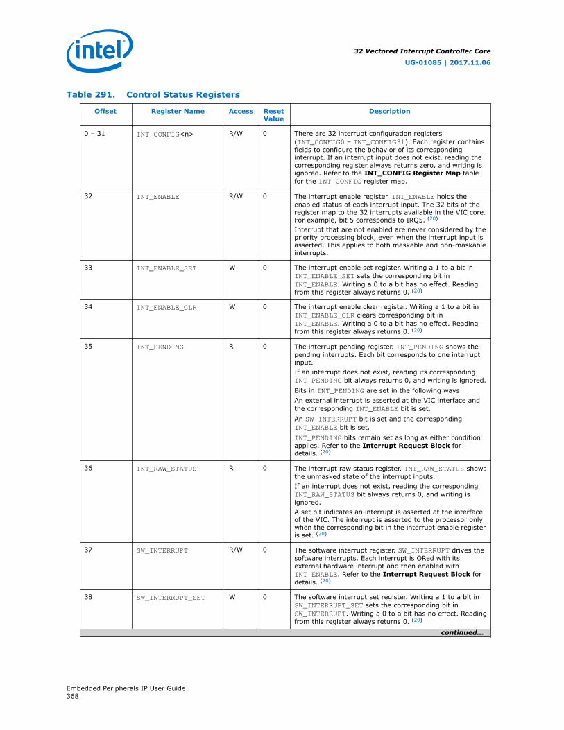
Table 291. Control Status Registers
Offset Register Name Access ResetValue
Description
0 – 31 INT_CONFIG<n> R/W 0 There are 32 interrupt configuration registers(INT_CONFIG0 – INT_CONFIG31). Each register containsfields to configure the behavior of its correspondinginterrupt. If an interrupt input does not exist, reading thecorresponding register always returns zero, and writing isignored. Refer to the INT_CONFIG Register Map tablefor the INT_CONFIG register map.
32 INT_ENABLE R/W 0 The interrupt enable register. INT_ENABLE holds theenabled status of each interrupt input. The 32 bits of theregister map to the 32 interrupts available in the VIC core.For example, bit 5 corresponds to IRQ5. (20)
Interrupt that are not enabled are never considered by thepriority processing block, even when the interrupt input isasserted. This applies to both maskable and non-maskableinterrupts.
33 INT_ENABLE_SET W 0 The interrupt enable set register. Writing a 1 to a bit inINT_ENABLE_SET sets the corresponding bit inINT_ENABLE. Writing a 0 to a bit has no effect. Readingfrom this register always returns 0. (20)
34 INT_ENABLE_CLR W 0 The interrupt enable clear register. Writing a 1 to a bit inINT_ENABLE_CLR clears corresponding bit inINT_ENABLE. Writing a 0 to a bit has no effect. Readingfrom this register always returns 0. (20)
35 INT_PENDING R 0 The interrupt pending register. INT_PENDING shows thepending interrupts. Each bit corresponds to one interruptinput.If an interrupt does not exist, reading its correspondingINT_PENDING bit always returns 0, and writing is ignored.Bits in INT_PENDING are set in the following ways:An external interrupt is asserted at the VIC interface andthe corresponding INT_ENABLE bit is set.An SW_INTERRUPT bit is set and the correspondingINT_ENABLE bit is set.INT_PENDING bits remain set as long as either conditionapplies. Refer to the Interrupt Request Block fordetails. (20)
36 INT_RAW_STATUS R 0 The interrupt raw status register. INT_RAW_STATUS showsthe unmasked state of the interrupt inputs.If an interrupt does not exist, reading the correspondingINT_RAW_STATUS bit always returns 0, and writing isignored.A set bit indicates an interrupt is asserted at the interfaceof the VIC. The interrupt is asserted to the processor onlywhen the corresponding bit in the interrupt enable registeris set. (20)
37 SW_INTERRUPT R/W 0 The software interrupt register. SW_INTERRUPT drives thesoftware interrupts. Each interrupt is ORed with itsexternal hardware interrupt and then enabled withINT_ENABLE. Refer to the Interrupt Request Block fordetails. (20)
38 SW_INTERRUPT_SET W 0 The software interrupt set register. Writing a 1 to a bit inSW_INTERRUPT_SET sets the corresponding bit inSW_INTERRUPT. Writing a 0 to a bit has no effect. Readingfrom this register always returns 0. (20)
continued...
32 Vectored Interrupt Controller Core
UG-01085 | 2017.11.06
Embedded Peripherals IP User Guide368
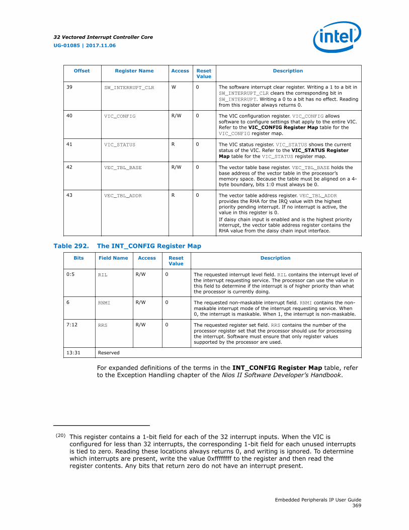
Offset Register Name Access ResetValue
Description
39 SW_INTERRUPT_CLR W 0 The software interrupt clear register. Writing a 1 to a bit inSW_INTERRUPT_CLR clears the corresponding bit inSW_INTERRUPT. Writing a 0 to a bit has no effect. Readingfrom this register always returns 0.
40 VIC_CONFIG R/W 0 The VIC configuration register. VIC_CONFIG allowssoftware to configure settings that apply to the entire VIC.Refer to the VIC_CONFIG Register Map table for theVIC_CONFIG register map.
41 VIC_STATUS R 0 The VIC status register. VIC_STATUS shows the currentstatus of the VIC. Refer to the VIC_STATUS RegisterMap table for the VIC_STATUS register map.
42 VEC_TBL_BASE R/W 0 The vector table base register. VEC_TBL_BASE holds thebase address of the vector table in the processor’smemory space. Because the table must be aligned on a 4-byte boundary, bits 1:0 must always be 0.
43 VEC_TBL_ADDR R 0 The vector table address register. VEC_TBL_ADDRprovides the RHA for the IRQ value with the highestpriority pending interrupt. If no interrupt is active, thevalue in this register is 0.If daisy chain input is enabled and is the highest priorityinterrupt, the vector table address register contains theRHA value from the daisy chain input interface.
Table 292. The INT_CONFIG Register Map
Bits Field Name Access ResetValue
Description
0:5 RIL R/W 0 The requested interrupt level field. RIL contains the interrupt level ofthe interrupt requesting service. The processor can use the value inthis field to determine if the interrupt is of higher priority than whatthe processor is currently doing.
6 RNMI R/W 0 The requested non-maskable interrupt field. RNMI contains the non-maskable interrupt mode of the interrupt requesting service. When0, the interrupt is maskable. When 1, the interrupt is non-maskable.
7:12 RRS R/W 0 The requested register set field. RRS contains the number of theprocessor register set that the processor should use for processingthe interrupt. Software must ensure that only register valuessupported by the processor are used.
13:31 Reserved
For expanded definitions of the terms in the INT_CONFIG Register Map table, referto the Exception Handling chapter of the Nios II Software Developer’s Handbook.
(20) This register contains a 1-bit field for each of the 32 interrupt inputs. When the VIC isconfigured for less than 32 interrupts, the corresponding 1-bit field for each unused interruptsis tied to zero. Reading these locations always returns 0, and writing is ignored. To determinewhich interrupts are present, write the value 0xffffffff to the register and then read theregister contents. Any bits that return zero do not have an interrupt present.
32 Vectored Interrupt Controller Core
UG-01085 | 2017.11.06
Embedded Peripherals IP User Guide369
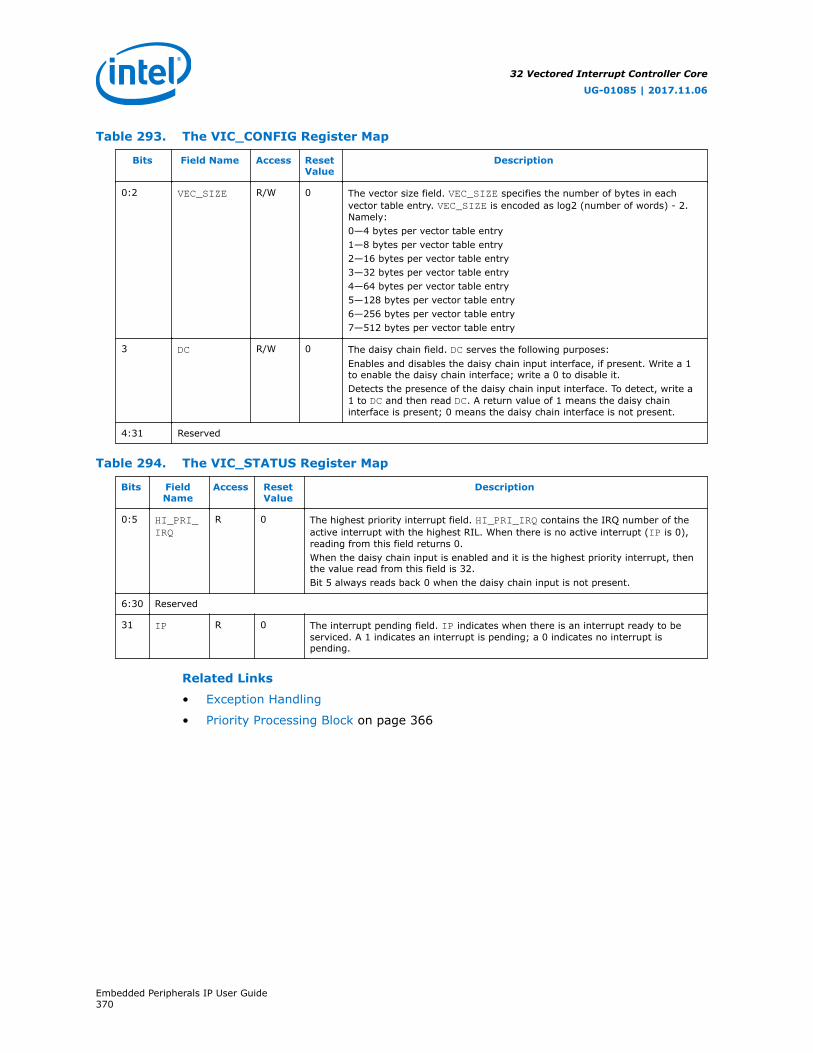
Table 293. The VIC_CONFIG Register Map
Bits Field Name Access ResetValue
Description
0:2 VEC_SIZE R/W 0 The vector size field. VEC_SIZE specifies the number of bytes in eachvector table entry. VEC_SIZE is encoded as log2 (number of words) - 2.Namely:0—4 bytes per vector table entry1—8 bytes per vector table entry2—16 bytes per vector table entry3—32 bytes per vector table entry4—64 bytes per vector table entry5—128 bytes per vector table entry6—256 bytes per vector table entry7—512 bytes per vector table entry
3 DC R/W 0 The daisy chain field. DC serves the following purposes:Enables and disables the daisy chain input interface, if present. Write a 1to enable the daisy chain interface; write a 0 to disable it.Detects the presence of the daisy chain input interface. To detect, write a1 to DC and then read DC. A return value of 1 means the daisy chaininterface is present; 0 means the daisy chain interface is not present.
4:31 Reserved
Table 294. The VIC_STATUS Register Map
Bits FieldName
Access ResetValue
Description
0:5 HI_PRI_IRQ
R 0 The highest priority interrupt field. HI_PRI_IRQ contains the IRQ number of theactive interrupt with the highest RIL. When there is no active interrupt (IP is 0),reading from this field returns 0.When the daisy chain input is enabled and it is the highest priority interrupt, thenthe value read from this field is 32.Bit 5 always reads back 0 when the daisy chain input is not present.
6:30 Reserved
31 IP R 0 The interrupt pending field. IP indicates when there is an interrupt ready to beserviced. A 1 indicates an interrupt is pending; a 0 indicates no interrupt ispending.
Related Links
• Exception Handling
• Priority Processing Block on page 366
32 Vectored Interrupt Controller Core
UG-01085 | 2017.11.06
Embedded Peripherals IP User Guide370
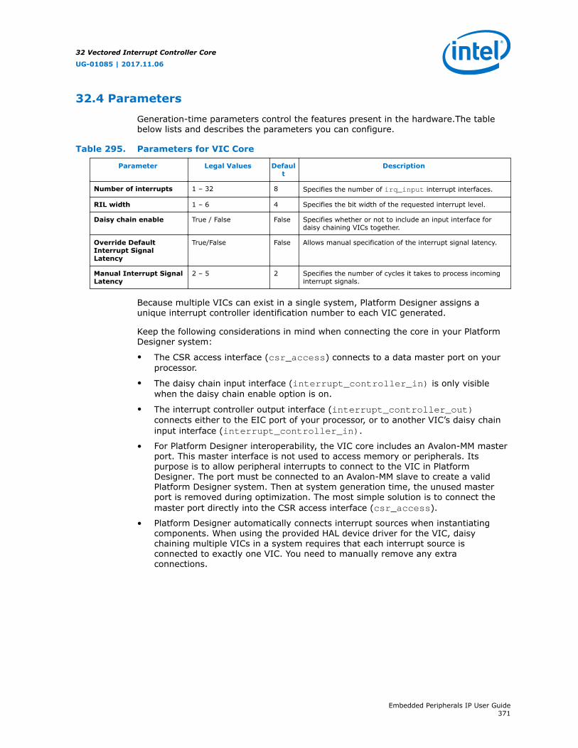
32.4 Parameters
Generation-time parameters control the features present in the hardware.The tablebelow lists and describes the parameters you can configure.
Table 295. Parameters for VIC Core
Parameter Legal Values Default
Description
Number of interrupts 1 – 32 8 Specifies the number of irq_input interrupt interfaces.
RIL width 1 – 6 4 Specifies the bit width of the requested interrupt level.
Daisy chain enable True / False False Specifies whether or not to include an input interface fordaisy chaining VICs together.
Override DefaultInterrupt SignalLatency
True/False False Allows manual specification of the interrupt signal latency.
Manual Interrupt SignalLatency
2 – 5 2 Specifies the number of cycles it takes to process incominginterrupt signals.
Because multiple VICs can exist in a single system, Platform Designer assigns aunique interrupt controller identification number to each VIC generated.
Keep the following considerations in mind when connecting the core in your PlatformDesigner system:
• The CSR access interface (csr_access) connects to a data master port on yourprocessor.
• The daisy chain input interface (interrupt_controller_in) is only visiblewhen the daisy chain enable option is on.
• The interrupt controller output interface (interrupt_controller_out)connects either to the EIC port of your processor, or to another VIC’s daisy chaininput interface (interrupt_controller_in).
• For Platform Designer interoperability, the VIC core includes an Avalon-MM masterport. This master interface is not used to access memory or peripherals. Itspurpose is to allow peripheral interrupts to connect to the VIC in PlatformDesigner. The port must be connected to an Avalon-MM slave to create a validPlatform Designer system. Then at system generation time, the unused masterport is removed during optimization. The most simple solution is to connect themaster port directly into the CSR access interface (csr_access).
• Platform Designer automatically connects interrupt sources when instantiatingcomponents. When using the provided HAL device driver for the VIC, daisychaining multiple VICs in a system requires that each interrupt source isconnected to exactly one VIC. You need to manually remove any extraconnections.
32 Vectored Interrupt Controller Core
UG-01085 | 2017.11.06
Embedded Peripherals IP User Guide371
32.5 to Intel FPGA HAL Software Programming Model
The Intel-provided driver implements a HAL device driver that integrates with a HALboard support package (BSP) for Nios II systems. HAL users should access the VICcore via the familiar HAL API.
32.5.1 Software Files
The VIC driver includes the following software files. These files provide low-levelaccess to the hardware and drivers that integrate with the Nios II HAL BSP. Applicationdevelopers should not modify these files.
• altera_vic_regs.h—Defines the core’s register map, providing symbolicconstants to access the low-level hardware.
• altera_vic_funnel.h, altera_vic_irq.h, altera_vic_irq.h,altera_vic_irq_init.h—Define the prototypes and macros necessary for theVIC driver.
• altera_vic.c, altera_vic_irq_init.c, altera_vic_isr_register.c,altera_vic_sw_intr.c, altera_vic_set_level.c,altera_vic_funnel_non_preemptive_nmi.S,altera_vic_funnel_non_preemptive.S, and altera_vic_funnel_preemptive.S—Provide the code that implements the VIC driver.
• altera_<name>_vector_tbl.S—Provides a vector table file for each VIC in thesystem. The BSP generator creates these files.
32.5.2 Macros
Macros to access all of the registers are defined in altera_vic_regs.h. For example,this file includes macros to access the INT_CONFIG register, including the followingmacros:
#define IOADDR_ALTERA_VIC_INT_CONFIG(base, irq) __IO_CALC_ADDRESS_NATIVE(base, irq)#define IORD_ALTERA_VIC_INT_CONFIG(base, irq) IORD(base, irq)#define IOWR_ALTERA_VIC_INT_CONFIG(base, irq, data) IOWR(base, irq,data)#define ALTERA_VIC_INT_CONFIG_RIL_MSK (0x3f)#define ALTERA_VIC_INT_CONFIG_RIL_OFST (0)#define ALTERA_VIC_INT_CONFIG_RNMI_MSK (0x40)#define ALTERA_VIC_INT_CONFIG_RNMI_OFST (6)#define ALTERA_VIC_INT_CONFIG_RRS_MSK (0x1f80)#define ALTERA_VIC_INT_CONFIG_RRS_OFST (7)
For a complete list of predefined macros and utilities to access the VIC hardware, referto the following files:
• <install_dir>\ip\altera\altera_vectored_interrupt_controller\top\inc\altera_vic_regs.h
• <install_dir>\ip\altera\altera_vectored_interrupt_controller\top\HAL\inc\altera_vic_funnel.h
• <install_dir>\ip\altera\altera_vectored_interrupt_controller\top\HAL\inc\altera_vic_irq.h
32 Vectored Interrupt Controller Core
UG-01085 | 2017.11.06
Embedded Peripherals IP User Guide372
32.5.3 Data Structure
Example 10. Device Data Structure
#define ALT_VIC_MAX_INTR_PORTS (32)
typedef struct alt_vic_dev{ void *base; /* Base address of VIC */ alt_u32 intr_controller_id; /* Interrupt controller ID */ alt_u32 num_of_intr_ports; /* Number of interrupt ports */ alt_u32 ril_width; /* RIL width */ alt_u32 daisy_chain_present; /* Daisy-chain input present */ alt_u32 vec_size; /* Vector size */ void *vec_addr; /* Vector table base address */ alt_u32 int_config[ALT_VIC_MAX_INTR_PORTS]; /* INT_CONFIG settings for each interrupt */
} alt_vic_dev;
32.5.4 VIC API
The VIC device driver provides all the routines required of an to Intel FPGA HALexternal interrupt controller (EIC) device driver. The following functions are requiredby the Nios II enhanced HAL interrupt API:
• alt_ic_isr_register ()
• alt_ic_irq_enable()
• alt_ic_irq_disable()
• alt_ic_irq_enabled()
These functions write to the register map to change the setting or read from theregister map to check the status of the VIC component thru a memory-mappedaddress.
For detailed descriptions of these functions, refer to the to the HAL API Referencechapter of the Nios II Software Developer’s Handbook.
The table below lists the API functions specific to the VIC core and brieflydescribes each. Details of each function follow the table.
Table 296. Function List
Name Description
alt_vic_sw_interrupt_set() Sets the corresponding bit in the SW_INTERRUPT register toenable a given interrupt via software.
alt_vic_sw_interrupt_clear() Clears the corresponding bit in the SW_INTERRUPT registerto disable a given interrupt via software.
alt_vic_sw_interrupt_status() Reads the status of the SW_INTERRUPT register for a giveninterrupt.
alt_vic_irq_set_level() Sets the interrupt level for a given interrupt.
Related Links
HAL API Reference
32 Vectored Interrupt Controller Core
UG-01085 | 2017.11.06
Embedded Peripherals IP User Guide373

32.5.4.1 alt_vic_sw_interrupt_set()
Prototype: int alt_vic_sw_interrupt_set(alt_u32 ic_id, alt_u32 irq)
Thread-safe: No
Available fromISR:
No
Include: altera_vic_irq.h, altera_vic_regs.h
Parameters: ic_id—the interrupt controller identification number as defined in system.hirq—the interrupt value as defined in system.h
Returns: Returns zero if successful; otherwise non-zero for one or more of the following reasons:The value in ic_id is invalidThe value in irq is invalid
Description: Triggers a single software interrupt
32.5.4.2 alt_vic_sw_interrupt_clear()
Prototype: int alt_vic_sw_interrupt_clear(alt_u32 ic_id, alt_u32 irq)
Thread-safe: No
Available fromISR:
Yes; if interrupt preemption is enabled, disable global interrupts before calling this routine.
Include: altera_vic_irq.h, altera_vic_regs.h
Parameters: ic_id—the interrupt controller identification number as defined in system.hirq—the interrupt value as defined in system.h
Returns: Returns zero if successful; otherwise non-zero for one or more of the following reasons:The value in ic_id is invalidThe value in irq is invalid
Description: Clears a single software interrupt
32.5.4.3 alt_vic_sw_interrupt_status()
Prototype: alt_u32 alt_vic_sw_interrupt_status(alt_u32 ic_id, alt_u32 irq)
Thread-safe: No
Available fromISR:
Yes; if interrupt preemption is enabled, disable global interrupts before calling this routine.
Include: altera_vic_irq.h, altera_vic_regs.h
Parameters: ic_id—the interrupt controller identification number as defined in system.hirq—the interrupt value as defined in system.h
Returns: Returns non-zero if the corresponding software trigger interrupt is active; otherwise zero for one ormore of the following reasons:The corresponding software trigger interrupt is disabledThe value in ic_id is invalidThe value in irq is invalid
Description: Checks the software interrupt status for a single interrupt
32 Vectored Interrupt Controller Core
UG-01085 | 2017.11.06
Embedded Peripherals IP User Guide374

32.5.4.4 alt_vic_irq_set_level()
Prototype: int alt_vic_irq_set_level(alt_u32 ic_id, alt_u32 irq, alt_u32 level)
Thread-safe: No
Available fromISR:
No
Include: altera_vic_irq.h, altera_vic_regs.h
Parameters: ic_id—the interrupt controller identification number as defined in system.hirq—the interrupt value as defined in system.hlevel—the interrupt level to set
Returns: Returns zero if successful; otherwise non-zero for one or more of the following reasons:The value in ic_id is invalidThe value in irq is invalidThe value in level is invalid
Description: Sets the interrupt level for a single interrupt.Intel recommends setting the interrupt level only to zero to disable the interrupt or to the originalvalue specified in your BSP. Writing any other value could violate the overlapping register set,priority level, and other design rules. Refer to the VIC BSP Design Rules for to Intel FPGA HALImplementation section for more information.
32.5.5 Run-time Initialization
During system initialization, software configures the each VIC instance's controlregisters using settings specified in the BSP. The RIL, RRS, and RNMI fields are writteninto the interrupt configuration register of each interrupt port in each VIC. Allinterrupts are disabled until other software registers a handler using thealt_ic_isr_register() API.
32.5.6 Board Support Package
The BSP you generate for your Nios II system provides access to the hardware in yoursystem, including the VIC. The VIC driver includes scripts that the BSP generator callsto get default interrupt settings and to validate settings during BSP generation. TheNios II BSP Editor provides a mechanism to edit these settings and generate a BSP foryour Platform Designer design.
The generator produces a vector table file for each VIC in the system, namedaltera_<name>_vector_tbl.S. The vector table's source path is added to the BSPMakefile for compilation along with other VIC driver source code. Its contents arebased on the BSP settings for each VIC's interrupt ports.
The VIC does not support runtime stack checking feature(hal.enable_runtime_stack_checking) in the BSP setting.
VIC BSP Settings
The VIC driver scripts provide settings to the BSP. The number and naming of thesesettings depends on your hardware system's configuration, specifically, the number ofoptional shadow register sets in the Nios II processor, the number of VIC controllers inthe system, and the number of interrupt ports each VIC has.
32 Vectored Interrupt Controller Core
UG-01085 | 2017.11.06
Embedded Peripherals IP User Guide375
Certain settings apply to all VIC instances in the system, while others apply to aspecific VIC instance. Settings that apply to each interrupt port apply only to thespecified interrupt port number on that VIC instance.
The remainder of this section lists details and descriptions of each VIC BSP setting.
32.5.6.1 altera_vic_driver.enable_preemption
Identifier: ALTERA_VIC_DRIVER_ISR_PREEMPTION_ENABLED
Type: BooleanDefineOnly
Default value: 1 when all components connected to the VICs supportpreemption. 0 when any of the connected components don’tsupport preemption.
Destination file: system.h
Description: Enables global interrupt preemption (nesting). Whenenabled (set to 1), the macroALTERA_VIC_DRIVER_ISR_PREEMPTION_ENABLED isdefined in system.h.Two types of ISR preemption are available. This settingmust be enabled along with other settings to enable specifictypes of preemption.All preemption settings are dependant on whether thedevice drivers in your BSP support interrupt preemption. Formore information about preemption, refer to the ExceptionHandling chapter of the Nios II Software Developer’sHandbook.
Occurs: Once per VIC
32.5.6.2 altera_vic_driver.enable_preemption_into_new_register_set
Identifier: ALTERA_VIC_DRIVER_PREEMPTION_INTO_NEW_REGISTER_SET_ENABLED
Type: BooleanDefineOnly
Default value: 0
Destination file: system.h
Description: Enables interrupt preemption (nesting) if a higher priorityinterrupt is asserted while a lower priority ISR is executing,and that higher priority interrupt uses a different registerset than the interrupt currently being serviced.When this setting is enabled (set to 1), the macroALTERA_VIC_DRIVER_ISR_PREEMPTION_INTO_NEW_REGISTER_SET_ENABLED is defined in system.h and the NiosII config.ANI (automatic nested interrupts) bit is assertedduring system software initialization.Use this setting to limit interrupt preemption to higherpriority (RIL) interrupts that use a different register set thana lower priority interrupt that might be executing. Thissetting allows you to support some preemption whilemaintaining the lowest possible interrupt response time.However, this setting does not allow an interrupt at a higherpriority (RIL) to preempt a lower priority interrupt if thehigher priority interrupt is assigned to the same register setas the lower priority interrupt.
Occurs: Once per VIC
32 Vectored Interrupt Controller Core
UG-01085 | 2017.11.06
Embedded Peripherals IP User Guide376

32.5.6.3 altera_vic_driver.enable_preemption_rs_<n>
Identifier: ALTERA_VIC_DRIVER_ENABLE_PREEMPTION_RS_<n>
Type: Boolean
Default value: 0
Destination file: system.h
Description: Enables interrupt preemption (nesting) if a higher priorityinterrupt is asserted while a lower priority ISR is executing,for all interrupts that target the specified register setnumber.When this setting is enabled (set to 1), the vector table foreach VIC utilizes a special interrupt funnel that managespreemption. All interrupts on all VIC instances assigned tothat register set then use this funnel.When a higher priority interrupt preempts a lower priorityinterrupt running in the same register set, the interruptfunnel detects this condition and saves the processorregisters to the stack before calling the higher priority ISR.The funnel code restores registers and allows the lowerpriority ISR to continue running once the higher priority ISRcompletes.Because this funnel contains additional overhead, enablingthis setting increases interrupt response time substantiallyfor all interrupts that target a register set where this type ofpreemption is enabled.Use this setting if you must guarantee that a higher priorityinterrupt preempts a lower priority interrupt, and youassigned multiple interrupts at different priorities to thesame Nios II shadow register set.
Occurs: Per register set; <n> refers to the register set number.
32.5.6.4 altera_vic_driver.linker_section
Identifier: ALTERA_VIC_DRIVER_LINKER_SECTION
Type: UnquotedString
Default value: .text
Destination file: system.h
Description: Specifies the linker section that each VIC's generated vectortable and each interrupt funnel link to. The memory devicethat the specified linker section is mapped to must beconnected to both the Nios II instruction and data mastersin your Platform Designer system.Use this setting to link performance-critical code into fastermemory. For example, if your system's code is in DRAM andyou have an on-chip or tightly-coupled memory interface forinterrupt handling code, assigning the VIC driver linkersection to a section in that memory improves interruptresponse time.For more information about linker sections and the Nios IIBSP Editor, refer to the Getting Started with theGraphical User Interface chapter of the Nios II SoftwareDeveloper’s Handbook.
Occurs: Once per VIC
32 Vectored Interrupt Controller Core
UG-01085 | 2017.11.06
Embedded Peripherals IP User Guide377

32.5.6.5 altera_vic_driver.<name>.vec_size
Identifier: <name>_VEC_SIZE
Type: DecimalNumber
Default value: 16
Destination file: system.h
Description: Specifies the number of bytes in each vector table entry.Legal values are 16, 32, 64, 128, 256, and 512.The generated VIC vector tables in the BSP require aminimum of 16 bytes per entry.If you intend to write your own vector table or locate yourISR at the vector address, you can use a larger size.The vector table's total size is equal to the number ofinterrupt ports on the VIC instance multiplied by the vectortable entry size specified in this setting.
Occurs: Per instance; <name> refers to the component name youassign in Platform Designer.
32.5.6.6 altera_vic_driver.<name>.irq<n>_rrs
Identifier: ALTERA_VIC_DRIVER_<name>_IRQ<n>_RRS
Type: DecimalNumber
Default value: Refer to the Default Settings for RRS and RIL section.
Destination file: system.h
Description: Specifies the RRS for the interrupt connected to thecorresponding port. Legal values are 1 to the number ofshadow register sets defined for the processor.
Occurs: Per IRQ per instance; <name> refers to the VIC’s name and<n> refers to the IRQ number that you assign in PlatformDesigner. Refer to Platform Designer to determine whichIRQ numbers correspond to which components in yourdesign.
32.5.6.7 altera_vic_driver.<name>.irq<n>_ril
Identifier: ALTERA_VIC_DRIVER_<name>_IRQ<n>_RIL
Type: DecimalNumber
Default value: Refer to Default Settings for RRS and RIL section.
Destination file: system.h
Description: Specifies the RIL for the interrupt connected to thecorresponding port. Legal values are 0 to 2RIL width -1.
Occurs: Per IRQ per instance; <name> refers to the VIC’s name and<n> refers to the IRQ number that you assign in PlatformDesigner. Refer to Platform Designer to determine whichIRQ numbers correspond to which components in yourdesign.
32 Vectored Interrupt Controller Core
UG-01085 | 2017.11.06
Embedded Peripherals IP User Guide378
32.5.6.8 altera_vic_driver.<name>.irq<n>_rnmi
Identifier: ALTERA_VIC_DRIVER_<name>_IRQ<n>_RNMI
Type: Boolean
Default value: 0
Destination file: system.h
Description: Specifies whether the interrupt port is a maskable or non-maskable interrupt (NMI). Legal values are 0 and 1. Whenset to 0, the port is maskable. NMIs cannot be disabled inhardware and there are several restrictions imposed for theRIL and RRS settings associated with any interrupt with NNIenabled.
Occurs: Per IRQ per instance; <name> refers to the VIC’s name and<n> refers to the IRQ number that you assign in PlatformDesigner. Refer to Platform Designer to determine whichIRQ numbers correspond to which components in yourdesign.
32.5.6.9 Default Settings for RRS and RIL
The default assignment of RRS and RIL values for each interrupt assumes interruptport 0 on the VIC instance attached to your processor is the highest priority interrupt,with successively lower priorities as the interrupt port number increases. Interruptports on other VIC instances connected through the first VIC's daisy chain interfaceare assigned successively lower priorities.
To make effective use of the VIC interrupt setting defaults, assign your highest priorityinterrupts to low interrupt port numbers on the VIC closest to the processor. Assignlower priority interrupts and interrupts that do not need exclusive access to a shadowregister set, to higher interrupt port numbers, or to another daisy-chained VIC.
The following steps describe the algorithm for default RIL assignment:
1. The formula 2RIL width -1 is used to calculate the maximum RIL value.
2. interrupt port 0 on the VIC connected to the processor is assigned the highestpossible RIL.
3. The RIL value is decremented and assigned to each subsequent interrupt port insuccession until the RIL value is 1.
4. The RILs for all remaining interrupt ports on all remaining VICs in the chain areassigned 1.
The following steps describe the algorithm for default RRS assignment:
5. The highest register set number is assigned to the interrupt with the highestpriority.
6. Each subsequent interrupt is assigned using the same method as the default RILassignment.
For example, consider a system with two VICs, VIC0 and VIC1. Each VIC has anRIL width of 3, and each has 4 interrupt ports. VIC0 is connected to the processorand VIC1 to the daisy chain interface on VIC0. The processor has 3 shadowregister sets.
32 Vectored Interrupt Controller Core
UG-01085 | 2017.11.06
Embedded Peripherals IP User Guide379

Table 297. Default RRS and RIL Assignment Example
VIC IRQ RRS RIL
0 0 3 7
0 1 2 6
0 2 1 5
0 3 1 4
1 0 1 3
1 1 1 2
1 2 1 1
1 3 1 1
32.5.6.10 VIC BSP Design Rules for to Intel FPGA HAL Implementation
The VIC BSP settings allow for a large number of combinations. This list describessome basic design rules to follow to ensure a functional BSP:
• Each component’s interrupt interface in your system should only be connected toone VIC instance per processor.
• The number of shadow register sets for the processor must be greater than zero.
• RRS values must always be greater than zero and less than or equal to thenumber of shadow register sets.
• RIL values must always be greater than zero and less than or equal to themaximum RIL.
• All RILs assigned to a register set must be sequential to avoid a higher priorityinterrupt overwriting contents of a register set being used by a lower priorityinterrupt.
Note: The Nios II BSP Editor uses the term “overlap condition” to refer to nonsequential RILassignments.
• NMIs cannot share register sets with maskable interrupts.
• NMIs must have RILs set to a number equal to or greater than the highest RIL ofany maskable interrupt. When equal, the NMIs must have a lower logical interruptport number than any maskable interrupt.
• The vector table and funnel code section's memory device must connect to a datamaster and an instruction master.
• NMIs must use funnels with preemption disabled.
• When global preemption is disabled, enabling preemption into a new register setor per-register-set preemption might produce unpredictable results. Be sure thatall interrupt service routines (ISR) used by the register set support preemption.
• Enabling register set preemption for register sets with peripherals that don'tsupport preemption might result in unpredictable behavior.
32 Vectored Interrupt Controller Core
UG-01085 | 2017.11.06
Embedded Peripherals IP User Guide380
32.5.6.11 RTOS Considerations
BSPs configured to use a real time operating system (RTOS) might have additionalsoftware linked into the HAL interrupt funnel code using the ALT_OS_INT_ENTER andALT_OS_INT_EXIT macros. The exact nature and overhead of this code is RTOS-specific. Additional code adds to interrupt response and recovery time. Refer to yourRTOS documentation to determine if such code is necessary.
32.6 Implementing the VIC in Platform Designer
This section describes how to incorporate one or more VICs in your Platform Designersystem, and how to support the VIC in software.
32.6.1 Adding VIC Hardware
When you add a VIC to your Platform Designer system, you must perform thefollowing high-level tasks:
1. Add the EIC interface to your Nios II processor core
2. Optionally add shadow register sets to your Nios II processor core (required if youintend to use HAL interrupt support)
3. Add and parameterize one or more VIC components
4. Connect interrupt sources to the VIC component(s)
32.6.1.1 Adding the EIC Interface Shadow Register Set
This section describes how to add the EIC interface and shadow register sets to a NiosII processor core in Platform Designer, through the parameter editor interface.
1. In Platform Designer, double-click the Nios II processor to open the parametereditor interface.
2. Enable the EIC interface on the Nios II processor by selecting it in the InterruptController list in the Advanced Features tab, as shown in the figure below.
There are two options for Interrupt Controller: Internal and External. If youselect Internal, the processor is implemented with the internal interruptcontroller. Select External to implement the processor with an EIC interface.
Note: When you implement the EIC interface, you must connect an EIC, such asthe VIC. Failure to connect an EIC results in a Platform Designer error.
3. Select the desired number of shadow register sets. In the Number of shadowregister sets list, select the number of register sets that matches your systemperformance goals.
4. Click Finish to exit from the Nios II parameter editor interface . Notice that theprocessor shows an unconnected interrupt_controller_in Avalon-ST sink,as shown in the figure below.
32 Vectored Interrupt Controller Core
UG-01085 | 2017.11.06
Embedded Peripherals IP User Guide381

Figure 98. Configuring the Interrupt Controller and Shadow Register Sets
Figure 99. Nios II Processor with EIC Interface
Shadow register sets reduce the context switching overhead associated with savingand restoring registers, which can otherwise be significant. If possible, add oneshadow register set for each interrupt that requires high performance.
32 Vectored Interrupt Controller Core
UG-01085 | 2017.11.06
Embedded Peripherals IP User Guide382
32.6.1.2 VIC Instantiation, Parameterization, and Connection
After you add the EIC interface and shadow register set(s) to the Nios II processor,you must instantiate and parameterize the VIC in your Platform Designer system.
32.6.1.2.1 Instantiation
To instantiate a VIC in your Platform Designer system, execute the following steps:
1. Browse to the IP Catalog window in Platform Designer.
2. Type "vector" in the search box. The interface hides all components except theVIC, as shown in the figure below.
3. Double click the Vectored Interrupt Controller component to add this componentto your Platform Designer System.
Figure 100. Vectored Interrupt Controller Component
32 Vectored Interrupt Controller Core
UG-01085 | 2017.11.06
Embedded Peripherals IP User Guide383
32.6.1.2.2 Parameterization
When you add the VIC to your system, the Vectored Interrupt Controller interfaceappears as shown below.
Figure 101. Vectored Interrupt Controller Parameterization
The VIC interface allows you to specify the following options:
• Number of Interrupts—The number of interrupts your VIC must support.
• Requested Interrupt Level (RIL) Width—The number of bits allocated torepresent the interrupt level for each interrupt.
• DAISY_CHAIN_ENABLE—Allows the VIC to daisy chain to another EIC. Turn onthis option if you want to support multiple VICs in your system.
Note: Study the VIC Daisy-Chain example that accompanies this document for ausage example.
• Override Default Interrupt Signal Latency—Allows manual specification of theinterrupt signal latency.
• Manual Interrupt Signal Latency—Specifies the number of cycles it takes toprocess the incoming interrupt signals.
When you have finished parameterizing the VIC, click Finish to instantiate thecomponent in your Platform Designer system.
32 Vectored Interrupt Controller Core
UG-01085 | 2017.11.06
Embedded Peripherals IP User Guide384
32.6.1.2.3 VIC Connections
When you have added the VIC to your system, it appears in Platform Designer asshown below.
Note: If you have enabled daisy chaining, Platform Designer adds an Avalon-ST sink, calledinterrupt_controller_in, to the VIC.
Figure 102. VIC Interfaces
After adding a VIC to the Platform Designer system, you must parameterize the VICand the EIC interface at the system level. Immediately after you add the VIC, severalerror messages appear. Resolve these error messages by executing the followingactions in any order:
• Connect the VIC’s interrupt_controller_out Avalon-ST source to theinterrupt_controller_in Avalon-ST sink on either the Nios II processor orthe next VIC in a daisy-chained configuration.
• Connect the Nios II processor's data_master Avalon-MM ports to thecsr_access Avalon-MM slave port.
• Assign an interrupt number for each interrupt-based component in the system, asshown below. This step connects each component to an interrupt port on the VIC.
Note: If your system contains more than one EIC connected to a single processor, you mustensure that each component is connected to an interrupt port on only one EIC.
Figure 103. Assigning Interrupt Numbers
32 Vectored Interrupt Controller Core
UG-01085 | 2017.11.06
Embedded Peripherals IP User Guide385
When you use the HAL VIC driver, the driver makes a default assignment from registersets to interrupts. The default assignment makes some assumptions about interruptpriorities, based on how devices are connected to the VIC.
Note: To make effective use of the VIC interrupt setting defaults, assign your highest priorityinterrupts to low interrupt port numbers on the VIC closest to the processor.
32.6.2 Software for VIC
If you write an interrupt handler for a system based on the VIC component, you mustuse the HAL enhanced interrupt API to register the handler and control its runtimeenvironment. The enhanced interrupt API provides a number of functions for use withEICs, including the VIC. This section describes a subset of the functions in theenhanced interrupt API.
For information about the enhanced interrupt API, refer to “Interrupt ServiceRoutines” in the Exception Handling chapter of the Nios II Software Developer’sHandbook.
In particular, this section shows how to code a driver so that it supports both theenhanced API and the legacy API. This must include testing for the presence of theenhanced API, and conditionally calling the appropriate function.
Related Links
Interrupt Service Routines
32.6.2.1 alt_ic_isr_register() versus alt_irq_register()
The enhanced API function alt_ic_isr_register() is very similar to the legacyfunction alt_irq_register(), with a few important differences. The differencesbetween these two functions are best understood by examining the code in Registering an ISR with Both APIs on page 386. This example registers a timerinterrupt in either the legacy API or the enhanced API, whichever is implemented inthe board support package (BSP). The example is taken directly from the examplecode accompanying this document.
Example 11. Registering an ISR with Both APIs
#ifdef ALT_ENHANCED_INTERRUPT_API_PRESENTvoid timer_interrupt_latency_init (void* base, alt_u32 irq_controller_id, alt_u32 irq){ /* Register the interrupt */ alt_ic_isr_register(irq_controller_id, irq, timer_interrupt_latency_irq, base, NULL); /* Start timer */ IOWR_ALTERA_AVALON_TIMER_CONTROL(base, ALTERA_AVALON_TIMER_CONTROL_ITO_MSK | ALTERA_AVALON_TIMER_CONTROL_START_MSK);}#elsevoid timer_interrupt_latency_init (void* base, alt_u32 irq){ /* Register the interrupt */ alt_irq_register(irq, base, timer_interrupt_latency_irq); /* Start timer */ IOWR_ALTERA_AVALON_TIMER_CONTROL(base, ALTERA_AVALON_TIMER_CONTROL_ITO_MSK | ALTERA_AVALON_TIMER_CONTROL_START_MSK);}#endif
32 Vectored Interrupt Controller Core
UG-01085 | 2017.11.06
Embedded Peripherals IP User Guide386

The first line of Registering an ISR with Both APIs on page 386 detects whether theBSP implements the enhanced interrupt API. If the enhanced API is implemented, thetimer_interrupt_latency_init() function calls the enhanced function. If not,timer_interrupt_latency_init() reverts to the legacy interrupt API function.
For an explanation of how the Nios II Software Build Tools select which API toimplement in a BSP, refer to “Interrupt Service Routines” in the Exception Handlingchapter of the Nios II Software Developer’s Handbook.
Enhanced Function alt_ic_isr_register() on page 387 shows the function prototype foralt_ic_isr_register(), which registers an ISR in the enhanced API. The interruptcontroller identifier (for argument ic_id) and the interrupt port number (forargument irq) are defined in system.h.
Example 12. Enhanced Function alt_ic_isr_register()
extern int alt_ic_isr_register(alt_u32 ic_id, alt_u32 irq, alt_isr_func isr, void *isr_context, void *flags);
For comparison, Legacy Function alt_irq_register() on page 387 shows the functionprototype for alt_irq_register(), which registers an ISR in the legacy API.
Example 13. Legacy Function alt_irq_register()
extern int alt_irq_register (alt_u32 id, void* context, alt_isr_func handler);
The arguments passed into alt_ic_isr_register() are slightly different fromthose passed into alt_irq_register(). The table below compares the argumentsto the two functions.
Table 298. Arguments to alt_ic_isr_register() versus alt_irq_register()
alt_ic_isr_register() Argument Purpose alt_irq_register() Argument
alt_u32 ic_id Unique interrupt controller ID asdefined in system.h.
—
alt_u32 irq Interrupt request (IRQ) number asdefined in system.h.
alt_u32 id
alt_isr_func isr Interrupt service routine (ISR) functionpointer
handler
void* isr_context Optional pointer to a component-specific data structure.
context
void* flags Reserved. Other EIC implementationsmight use this argument.
None
There are other significant differences between the legacy interrupt API and theenhanced interrupt API. Some of these differences impact the ISR body itself. Notably,the two APIs employ completely different interrupt preemption models. The examplecode accompanying this document illustrates many of the differences.
32 Vectored Interrupt Controller Core
UG-01085 | 2017.11.06
Embedded Peripherals IP User Guide387
For further information about the other functions in the HAL interrupt APIs, refer tothe Exception Handling and HAL API Reference chapters of the Nios II SoftwareDeveloper’s Handbook.
Related Links
• Exception Handling
• HAL API Reference
32.7 Example Designs
This section provides a brief description of the example designs provided with thisdocument to demonstrate the usage of the VIC. Additionally, this section providesinstructions for running the software examples on the Cyclone V SoC development kit.
Related Links
VIC_collateral_cv.zip
32.7.1 Example Description
The example designs are provided in a file called VIC_collateral_cv.zip.VIC_collateral_cv.zip is available on the Documentation: Nios II Processor pageof the Intel FPGA website under Vectored Interrupt Controller Design Files.
Table 299. Example Designs in VIC_collateral_cv.zip
Example Name Folder Name Description
VIC Basic VIC_Example A single VIC
VIC Daisy-Chain VIC_DaisyChain_Example Two daisy-chained VICs
VIC Table-Resident VIC_ISRnVectorTable_Example VIC with ISR located in vector table
IIC VIC_noVIC_Example IIC example, for comparison with theVIC examples
The top-level folder in VIC_collateral_cv.zip, called VIC_collateral_cv, containsthe following files:
• run_sw.sh—Shell script to run one, several or all of the examples
• README.txt—Describes the .zip file contents
32 Vectored Interrupt Controller Core
UG-01085 | 2017.11.06
Embedded Peripherals IP User Guide388
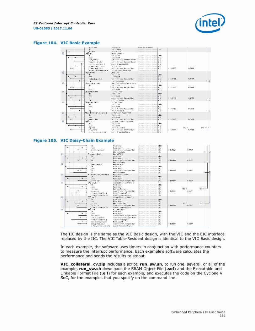
Figure 104. VIC Basic Example
Figure 105. VIC Daisy-Chain Example
The IIC design is the same as the VIC Basic design, with the VIC and the EIC interfacereplaced by the IIC. The VIC Table-Resident design is identical to the VIC Basic design.
In each example, the software uses timers in conjunction with performance countersto measure the interrupt performance. Each example’s software calculates theperformance and sends the results to stdout.
VIC_collateral_cv.zip includes a script, run_sw.sh, to run one, several, or all of theexample. run_sw.sh downloads the SRAM Object File (.sof) and the Executable andLinkable Format File (.elf) for each example, and executes the code on the Cyclone VSoC, for the examples that you specify on the command line.
32 Vectored Interrupt Controller Core
UG-01085 | 2017.11.06
Embedded Peripherals IP User Guide389

Note: run_sw.sh assumes that you have only one JTAG download cable connected to yourhost computer. If you have multiple JTAG cables, you must modify run_sw.sh tospecify the cable connected to your Cyclone V SoC development kit.
Related Links
• Documentation: Nios II Processor
• VIC_collateral_cv.zip
32.7.2 Example Usage
Initially, Intel recommends that you run each example design as distributed, to seethe example’s performance on your own hardware. Thereafter, you can modify any ofthe examples to investigate the VIC’s performance options, or customize the code foryou application.
Execute the following steps to run each example design:
1. Power up your Cyclone V SoC board.
2. Connect the USB cable.
3. Unzip the VIC_collateral_cv.zip file to a working directory, expanding foldernames.
Note: The path name to your working directory must not contain any spaces.
4. In a Nios II Command Shell, change to the top-level directory,VIC_collateral_cv.
5. At the command prompt, type the following command:
./run_sw.sh
The script shows a list of options.
6. Run run_sw.sh again, using a command-line option that specifies the exampleyou would like to run, or to run all of the examples. VIC Example on page 392shows a sample session.
The run_sw.sh script performs the following steps:
a. Parses the command line argument(s) to determine which example(s) to run
b. Downloads the .sof for the selected example
c. Downloads the .elf for the selected example
d. Starts nios2-terminal to capture the software’s output
32.7.3 Software Description
The software for the various example designs is very similar. For example, thedifference between the software for the VIC Basic example and the software for theIIC example is the printf() call that generates the output to the terminal.
32 Vectored Interrupt Controller Core
UG-01085 | 2017.11.06
Embedded Peripherals IP User Guide390

All of the software performs the following steps:
1. Configures the timer used for measurement purposes
2. Registers an interrupt service routine (ISR)
3. Sets a global variable to 0xfeedface
4. Starts the performance counter to measure the interrupt time
5. Waits for the ISR to set the global variable to 0xfacefeed
6. Stops the performance counter and computes the interrupt time
The VIC Daisy-Chain example performs the measurement for both VICs connected inthe daisy chain, shown in Figure 105 on page 389.
In all these design examples, the GCC compiler in Nios II SBT tool is set tooptimization level 2. Also, some settings are modified during BSP generation in orderto reduce the code size. All these setting can be found in the create-this-bsp scriptincluded in the design example. Note that the number of clock cycles shows in thesedesign examples will be differ from this document if the setting is different.
For details about how the VIC Table-Resident example code works, refer to“Positioning the ISR in the Vector Table”. For details about performance counter usagein the example software, refer to “Latency Measurement with the PerformanceCounter”.
32 Vectored Interrupt Controller Core
UG-01085 | 2017.11.06
Embedded Peripherals IP User Guide391
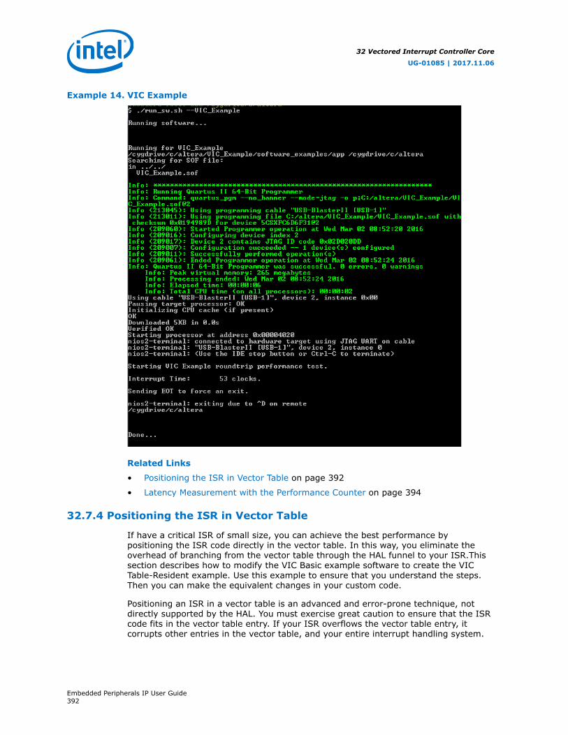
Example 14. VIC Example
Related Links
• Positioning the ISR in Vector Table on page 392
• Latency Measurement with the Performance Counter on page 394
32.7.4 Positioning the ISR in Vector Table
If have a critical ISR of small size, you can achieve the best performance bypositioning the ISR code directly in the vector table. In this way, you eliminate theoverhead of branching from the vector table through the HAL funnel to your ISR.Thissection describes how to modify the VIC Basic example software to create the VICTable-Resident example. Use this example to ensure that you understand the steps.Then you can make the equivalent changes in your custom code.
Positioning an ISR in a vector table is an advanced and error-prone technique, notdirectly supported by the HAL. You must exercise great caution to ensure that the ISRcode fits in the vector table entry. If your ISR overflows the vector table entry, itcorrupts other entries in the vector table, and your entire interrupt handling system.
32 Vectored Interrupt Controller Core
UG-01085 | 2017.11.06
Embedded Peripherals IP User Guide392

When locate your ISR in the vector table, it does not need to be registered. Do not callalt_ic_isr_register(), because it overwrites the contents of the vector table.
When the ISR is in the vector table, the HAL does not provide funnel code. Therefore,the ISR code must perform any context-switching actions normally handled by thefunnel. Funnel context switching can include some or all of the following actions:
• Saving and restoring registers
• Managing preemption
• Managing the stack pointer
To create the fastest possible ISR, minimize or eliminate the context-switching actionsyour ISR must perform by conforming to the following guidelines:
• Write the ISR in assembly language
• Assign a shadow register set for the ISR’s use
• Ensure that the ISR cannot be preempted by another ISR using the same registerset. By default, preemption within a register set is disabled on the Nios IIprocessor. You can also ensure this condition by giving the ISR exclusive access toits register set.
The VIC Table-Resident example requires modifying a BSP-generated file,altera_vic1_vector_tbl.S. If you regenerate the BSP after making thesemodifications, the Nios II Software Build Tools regenerate altera_vic1_vector_tbl.S,and your changes are overwritten.
Related Links
Software Description on page 390
32.7.4.1 Increase the Vector Table Entry Size
To insert the ISR in the vector table, you must increase the size of the vector entriesso that your entire ISR fits in a vector table entry. Use thealtera_vic_driver.<vic_instance>.vec_size BSP setting to adjust the vectortable entry size. On the Nios II Software Build Tools command line, you canmanipulate this setting with the --set command-line option. You can also modify thissetting in the Nios II BSP Editor.
In the VIC Table-Resident example, <vic_instance> is VIC1 and <size> is set to256 bytes.
32.7.4.2 Do Not Register the ISR
Remove the call to alt_ic_isr_register() for the interrupt that you place in thevector table. Replace it with an alt_ic_irq_enable() call. You must not callalt_ic_isr_register(), because it overwrites the contents of the vector table,destroying the body of your ISR.
32.7.4.3 Insert ISR in Vector Table
In the VIC Table-Resident example included with this document, the ISR code is in afile called vector.h in the BSP folder.
32 Vectored Interrupt Controller Core
UG-01085 | 2017.11.06
Embedded Peripherals IP User Guide393

To insert this code in the vector table, execute the following steps:
1. Generate the BSP by running the create-this-bsp script.
2. Modify altera_vic1_vector_tbl.S as shown in the example below.
Example 15. Modifications to Intel FPGA_vic1_vector_tbl.S
#include "altera_vic_funnel.h"#include "vector.h" /* ADD THIS LINE MANUALLY */ .section .text .align 2 .globl VIC1_VECTOR_TABLEVIC1_VECTOR_TABLE: MY_ISR 256 /* THIS LINE REPLACES THE FIRST VECTOR TABLE ENTRY */ ALT_SHADOW_NON_PREEMPTIVE_INTERRUPT 256 ALT_SHADOW_NON_PREEMPTIVE_INTERRUPT 256 ALT_SHADOW_NON_PREEMPTIVE_INTERRUPT 256 ALT_SHADOW_NON_PREEMPTIVE_INTERRUPT 256
After completion of these steps, build the software, run it, and observe the reportedinterrupt time. This example is about 18 clock cycles faster than the unmodified VICBasic example.
Some variation is likely for reasons discussed in “Real-Time Latency Concerns”.
Related Links
Real Time Latency Concerns on page 395
32.7.5 Latency Measurement with the Performance Counter
The Intel Quartus Prime enables you to make fast, accurate performancemeasurements. All examples included with this document use the PerformanceCounter component to measure interrupt latency.
The examples execute the following steps to measure the total time spent to servicean interrupt:
1. Initialize a global variable, interrupt_watch_value, to a known value,0xfeedface.
2. Set up a timer interrupt, registering an ISR that sets interrupt_watch_valueto 0xfacefeed.
3. Start the timer.
4. Wait in a while() loop until interrupt_watch_value becomes 0xfacefeed.
5. Immediately after exiting the while() loop, stop the performance counter,compute clock cycles and display the calculated value on stdout.
You can use similar methods to determine the real-time interrupt latencies in yoursystem.
Related Links
• Software Description on page 390
• Real Time Latency Concerns on page 395
32 Vectored Interrupt Controller Core
UG-01085 | 2017.11.06
Embedded Peripherals IP User Guide394

32.8 Advanced Topics
This section presents several topics that are useful for advanced interrupt handling.
32.8.1 Real Time Latency Concerns
This section presents an overview of interrupt latency, the elements that combine todetermine interrupt latency, and methods for measuring it. The following elementscomprise interrupt latency:
• Pipeline latency
• Cause latency
• Selection latency
• Funnel latency
• Compiler-related latency
Figure 106. The Elements of Interrupt Latency
Interrupt Request
Pipeline LatencyInterrupt Recovery(Back-end Funnel)
Interrupt Latency
Cause,Selection
&FunnelLatency
Background Background
ISR Code
Time
This section summarizes each element of latency and describes how to measurelatency. The accompanying example designs use the performance counter core tocapture all of the timing measurements. Performance counter core usage is describedin “Latency Measurement with the Performance Counter”.
Related Links
• Insert ISR in Vector Table on page 393
32 Vectored Interrupt Controller Core
UG-01085 | 2017.11.06
Embedded Peripherals IP User Guide395
• Latency Measurement with the Performance Counter on page 394
32.8.1.1 Pipeline Latency
Pipeline latency is defined as the number of clock cycles between an interrupt signalbeing asserted and the execution of the first instruction at the exception vector. It canvary widely, depending on the type of memory the processor is executing from andthe impact of other master ports in your hardware. Theoretically, this time could beinfinite if an ill-behaved master port blocks the processor from accessing memory,freezing the processor.
32.8.1.2 Cause Latency
Cause latency is the time required for the processor to identify an exception as ahardware interrupt. With an EIC, such as the VIC, the cause latency is zero becauseeach hardware interrupt has a dedicated interrupt vector address, separate from thesoftware exception vector address.
32.8.1.3 Selection Latency
Selection latency is the time required for the system to transfer control to the correctinterrupt vector, depending on which interrupt is triggered. The selection latency withthe VIC component depends on the number of interrupts that it services. The tablebelow outlines selection latency on a single VIC as a function of the number ofinterrupts.
Table 300. The Components of VIC Latency
Total Number ofInterrupts
Interrupt RequestClock Delay (clocks)
Priority ProcessingClock Delay (clocks)
Vector GenerationClock Delay (clocks)
Total InterruptLatency (clocks)
1 2 0 1 3
2—4 2 1 1 4
5—16 2 2 1 5
17—32 2 3 1 6
32.8.1.4 Funnel Latency
Funnel latency is the time required for the interrupt funnel to switch context. Funnellatency can include saving and restoring registers, managing preemption, andmanaging the stack pointer. Funnel latency depends on the following factors:
• Whether a separate interrupt stack is used
• The number of clock cycles required for load and store instructions
• Whether the interrupt requires switching to a different register set
• Whether the interrupt is preempting another interrupt within the same register set
• Whether preemption within the register set is allowed
Preemption within the register set requires special attention. The HAL VIC driverprovides special funnel code if an interrupt is allowed to preempt another interruptassigned to the same register set. In this case, the funnel incurs additional overheadto save and restore the register contents. When creating the BSP, you can controlpreemption within the register set by using the VIC driver’saltera_vic_driver_enable_preemption_rs_<n> setting.
32 Vectored Interrupt Controller Core
UG-01085 | 2017.11.06
Embedded Peripherals IP User Guide396
Note: With tightly-coupled memory, the Nios II processor can execute a load or storeinstruction in 1 clock cycle. With onchip memory, not tightly-coupled, the processorrequires two clock cycles.
Table 301. Single Stack HAL latency
Funnel Type Clock Cycles Required for Load or Store
1 2
Shadow register set, preemption withinthe register set disabled
10 13
Shadow register set, preemption withinthe register set enabled
42Same register set (sstatus.SRS=0)
64Same register set (sstatus.SRS=0)
26Different register set(sstatus.SRS=1)
32Different register set(sstatus.SRS=1)
Table 302. Separate Interrupt Stack HAL Latency
Funnel Type Clock Cycles Required for Load or Store
1 2
Shadow register set, preemption withinthe register set disabled
11Not preempting another interrupt(sstatus.IH=0)
14Not preempting another interrupt(sstatus.IH=0)
12Preempting another interrupt(sstatus.IH=1)
15Preempting another interrupt(sstatus.IH=1)
Shadow register set, preemption withinthe register set enabled
42Same register set (sstatus.SRS=0)
64Same register set (sstatus.SRS=0)
27• Different register set
(sstatus.SRS=1)
• Not preempting another interrupt(sstatus.IH=0)
33• Different register set
(sstatus.SRS=1)
• Not preempting another interrupt(sstatus.IH=0)
28• Different register set
(sstatus.SRS=1)
• Preempting another interrupt(sstatus.IH=1)
34• Different register set
(sstatus.SRS=1)
• Preempting another interrupt(sstatus.IH=1)
In the tables above, notice that the lowest latencies occur under the followingconditions:
• A different register set—Shadow register set switch; the ISR runs in a differentregister set from the interrupted task, eliminating any need to save or restoreregisters.
• Preemption (nesting) within the register set disabled.
Conversely, the highest latencies occur under the following conditions:
• The same register set—No shadow register set switch; the ISR runs in the sameregister set as the interrupted task, requiring the funnel code to save and restoreregisters.
• Preemption within the register set enabled.
32 Vectored Interrupt Controller Core
UG-01085 | 2017.11.06
Embedded Peripherals IP User Guide397

Of these two important factors, preemption makes the largest difference in latencies.With preemption disabled, much lower latencies occur regardless of other factors.
32.8.1.5 Compiler-Related Latency
The GNU C compiler creates a prologue and epilogue for many C functions, includingISRs. The prologue and epilogue are code sequences that take care of housekeepingtasks, such as saving and restoring context for the C runtime environment. The timerequired for the prologue and epilogue is called compiler-related latency.
The C compiler generates a prologue and epilogue as needed. If compiler optimizationis enabled, and the routine is compact, with few local variables, the prologue andepilogue are usually omitted. You can determine whether a prologue and epilogue aregenerated by examining the function’s assembly code.
Compiler latency normally has only a minor impact on overall interrupt servicingperformance. If you are concerned about compiler latency, you have two options:
• Enable compiler optimizations, and simplify your ISR, minimizing local variables.
• Write your ISR in assembly language.
32.8.2 Software Interrupt
Software can trigger any VIC interrupt by writing to the appropriate VIC control andstatus register (CSR). Software can trigger the interrupt connected to any hardwareinterrupt source, as well as interrupts that are not connected to hardware (software-only interrupts).
Triggering an interrupt from software is useful for debugging. Software can controlexactly when an interrupt is triggered, and measure the system’s interrupt response.
You can use a software-only interrupt to reprioritize an interrupt. An ISR that respondsto a high-priority hardware interrupt can perform the minimum processing required bythe hardware, and then trigger a software-only interrupt at a lower priority level tocomplete the interrupt processing.
The following functions are available for managing software interrupts:
• alt_vic_sw_interrupt_set()
• alt_vic_sw_interrupt_clear()
• alt_vic_sw_interrupt_status()
The implementations of these functions are in bsp/hal/drivers/src/altera_vic_sw_intr.c after you generate the BSP.
Note: You must define a value for the interrupt number in SOFT_IRQ.
Example 16. Registering a Software Interrupt
alt_ic_isr_register( VIC1_INTERRUPT_CONTROLLER_ID, SOFT_IRQ, soft_interrupt_latency_irq, NULL, NULL)
32 Vectored Interrupt Controller Core
UG-01085 | 2017.11.06
Embedded Peripherals IP User Guide398
Example 17. Registering a Timer Interrupt (for Comparison)
alt_ic_isr_register( LATENCY_TIMER_IRQ_INTERRUPT_CONTROLLER_ID, LATENCY_TIMER_IRQ, timer_interrupt_latency_irq, LATENCY_TIMER_BASE, NULL);
The following code generates a software interrupt:alt_vic_sw_interrupt_set(VIC1_INTERRUPT_CONTROLLER_ID, SOFT_IRQ);
32.9 Document Revision History
Table 303. Vectored Interrupt Controller Core History
Date Version Changes
May 2016 2016.05.03 Sections Added:• Implementing VIC in Platform Designer• Example Designs• Advanced Topics
Novemeber 2015 2015.11.06 Updated:• Table 288 on page 365• Table 290 on page 367• Table 295 on page 371
December 2013 v13.1.0 Updated the INT_ENABLE register description.
December 2010 v10.1.0 Added a note to to state that the VIC does not support the runtime stackchecking feature in BSP setting.Removed the “Device Support”, “Instantiating the Core in SOPC Builder”,and “Referenced Documents” sections.
July 2010 v10.0.0 No change from previous release.
November 2009 v9.1.0 Initial release.
32 Vectored Interrupt Controller Core
UG-01085 | 2017.11.06
Embedded Peripherals IP User Guide399
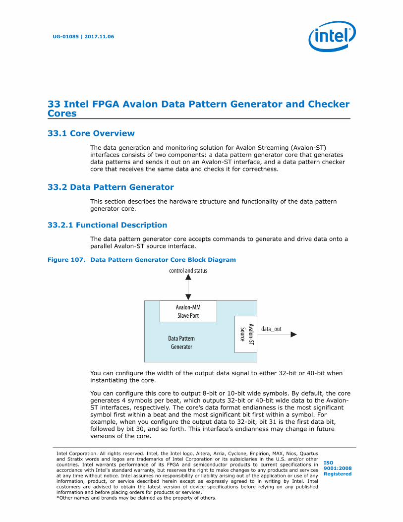
33 Intel FPGA Avalon Data Pattern Generator and CheckerCores
33.1 Core Overview
The data generation and monitoring solution for Avalon Streaming (Avalon-ST)interfaces consists of two components: a data pattern generator core that generatesdata patterns and sends it out on an Avalon-ST interface, and a data pattern checkercore that receives the same data and checks it for correctness.
33.2 Data Pattern Generator
This section describes the hardware structure and functionality of the data patterngenerator core.
33.2.1 Functional Description
The data pattern generator core accepts commands to generate and drive data onto aparallel Avalon-ST source interface.
Figure 107. Data Pattern Generator Core Block Diagram
data_out
control and status
Avalon-MMSlave Port
Data PatternGenerator
Avalon-STSource
You can configure the width of the output data signal to either 32-bit or 40-bit wheninstantiating the core.
You can configure this core to output 8-bit or 10-bit wide symbols. By default, the coregenerates 4 symbols per beat, which outputs 32-bit or 40-bit wide data to the Avalon-ST interfaces, respectively. The core’s data format endianness is the most significantsymbol first within a beat and the most significant bit first within a symbol. Forexample, when you configure the output data to 32-bit, bit 31 is the first data bit,followed by bit 30, and so forth. This interface’s endianness may change in futureversions of the core.
UG-01085 | 2017.11.06
Intel Corporation. All rights reserved. Intel, the Intel logo, Altera, Arria, Cyclone, Enpirion, MAX, Nios, Quartusand Stratix words and logos are trademarks of Intel Corporation or its subsidiaries in the U.S. and/or othercountries. Intel warrants performance of its FPGA and semiconductor products to current specifications inaccordance with Intel's standard warranty, but reserves the right to make changes to any products and servicesat any time without notice. Intel assumes no responsibility or liability arising out of the application or use of anyinformation, product, or service described herein except as expressly agreed to in writing by Intel. Intelcustomers are advised to obtain the latest version of device specifications before relying on any publishedinformation and before placing orders for products or services.*Other names and brands may be claimed as the property of others.
ISO9001:2008Registered

For smaller data widths, you can use the Avalon-ST Data Format Adapter for datawidth adaptation. The Avalon-ST Data Format Adapter converts the output from 4symbols per beat, to 2 or 1 symbol per beat. In this way, the 32-bit output of the corecan be adapted to a 16-bit or 8-bit output and the 40-bit output can be adapted to a20-bit or 10-bit output.
For more information about the Avalon-ST Data Format Adapter, refer to PlatformDesigner User Guide.
Control and Status Interface
The control and status interface is an Avalon-MM slave that allows you to enable ordisable the data generation. This interface also provides the run-time ability to choosedata pattern and inject an error into the data stream.
Output Interface
The output interface is a parallel Avalon-ST interface. You can configure the data widthat the output interface to suit your requirements.
Supported Data Patterns
The following data patterns are supported in the following manner, per beat. When thecore is disabled or in idle state, the default pattern generated on the data output is0×5555 (for 32-bit data width) or 0×55555 (for 40-bit data width).
Table 304. Supported Data Patterns (Binary Encoding)
Pattern 32-bit 40-bit
PRBS-7 PRBS in parallel PRBS in parallel
PRBS-15 PRBS in parallel PRBS in parallel
PRBS-23 PRBS in parallel PRBS in parallel
PRBS-31 PRBS in parallel PRBS in parallel
High Frequency 10101010 x 4 1010101010 x 4
Low Frequency 11110000 x 4 1111100000 x 4
Note to Table 29–1 :1. All PRBS patterns are seeded with 11111111.
This core does not support custom data patterns.
Inject Error
Errors can be injected into the data stream by controlling the Inject Error registerbits in the register map (refer to the Inject Error Field Descriptions table). Whenthe inject error bit is set, one bit of error is produced by inverting the LSB of the nextdata beat.
If the inject error bit is set before the core starts generating the data pattern, theerror bit is inserted in the first output cycle.
The Inject Error register bit is automatically reset after the error is introduced inthe pipeline, so that the next error can be injected.
33 Intel FPGA Avalon Data Pattern Generator and Checker Cores
UG-01085 | 2017.11.06
Embedded Peripherals IP User Guide401
Preamble Mode
The preamble mode is used for synchronization or word alignment. When thepreamble mode is set, the preamble control register sends the preamble character aspecified number of times before the selected pattern is generated, so the wordalignment block in the receiver can determine the word boundary in the bit stream.
The number of bits (Numbits) determines the number of cycles to output thepreamble character in the preamble mode. You can set the number of bits (Numbits)in the preamble control register. The default setting is 0 and the maximum value is255 bits. This mode can only be set when the data pattern generation core is disabled.
33.2.2 Configuration
You can configure your core by setting the following parameters in the PlatformDesigner:
• You can configure the input interface of the data pattern generator core using thefollowing parameter:
ST_DATA_W — The width of the input data signal that the data pattern checkercore supports. Valid values are 32, 40, 50, 64, 66, 80, and 128.
• You can add a bypass interface to register and output the input data through abypass port using the following parameter:
Enable Bypass Interface — Select this option to enable this interface. Bydefault, this interface is disabled.
• The data pattern generator core supports two types of interface: Avalon-ST andConduit interface. You can select either of them using the following parameter:
Enable Avalon Interface — Select this option to enable Avalon interface. Bydefault this interface is enabled. Deselect this option to enable Conduit interface.
• You can enable frequency counter by selecting the following parameter:
Enable Frequency Counter
• The following parameter determines the synchronization depth for clock crossingfrom Avalon-MM clock domain to Avalon-ST clock domain:
CROSS_CLK_SYNC_DEPTH — Default value is 2. Valid values are => 2.
33.3 Data Pattern Checker
This section describes the hardware structure and functionality of the data patternchecker core.
33.3.1 Functional Description
The data pattern checker core accepts data via an Avalon-ST sink interface, checks itfor correctness against the same predetermined pattern used by the data patterngenerator core or other PRBS generators to produce the data, and reports anyexceptions to the control interface.
33 Intel FPGA Avalon Data Pattern Generator and Checker Cores
UG-01085 | 2017.11.06
Embedded Peripherals IP User Guide402
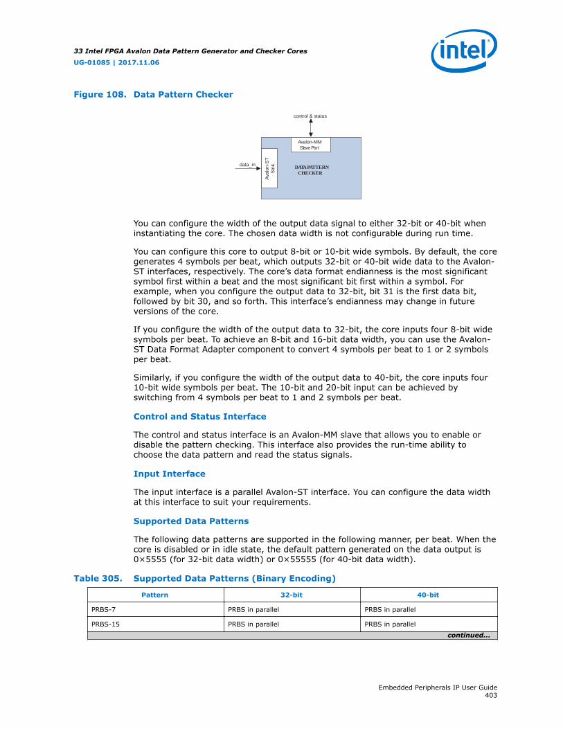
Figure 108. Data Pattern Checker
DATA PATTERN CHECKER
data_in
control & status
TS-nolav
Akni
S
Avalon-MM Slave Port
You can configure the width of the output data signal to either 32-bit or 40-bit wheninstantiating the core. The chosen data width is not configurable during run time.
You can configure this core to output 8-bit or 10-bit wide symbols. By default, the coregenerates 4 symbols per beat, which outputs 32-bit or 40-bit wide data to the Avalon-ST interfaces, respectively. The core’s data format endianness is the most significantsymbol first within a beat and the most significant bit first within a symbol. Forexample, when you configure the output data to 32-bit, bit 31 is the first data bit,followed by bit 30, and so forth. This interface’s endianness may change in futureversions of the core.
If you configure the width of the output data to 32-bit, the core inputs four 8-bit widesymbols per beat. To achieve an 8-bit and 16-bit data width, you can use the Avalon-ST Data Format Adapter component to convert 4 symbols per beat to 1 or 2 symbolsper beat.
Similarly, if you configure the width of the output data to 40-bit, the core inputs four10-bit wide symbols per beat. The 10-bit and 20-bit input can be achieved byswitching from 4 symbols per beat to 1 and 2 symbols per beat.
Control and Status Interface
The control and status interface is an Avalon-MM slave that allows you to enable ordisable the pattern checking. This interface also provides the run-time ability tochoose the data pattern and read the status signals.
Input Interface
The input interface is a parallel Avalon-ST interface. You can configure the data widthat this interface to suit your requirements.
Supported Data Patterns
The following data patterns are supported in the following manner, per beat. When thecore is disabled or in idle state, the default pattern generated on the data output is0×5555 (for 32-bit data width) or 0×55555 (for 40-bit data width).
Table 305. Supported Data Patterns (Binary Encoding)
Pattern 32-bit 40-bit
PRBS-7 PRBS in parallel PRBS in parallel
PRBS-15 PRBS in parallel PRBS in parallel
continued...
33 Intel FPGA Avalon Data Pattern Generator and Checker Cores
UG-01085 | 2017.11.06
Embedded Peripherals IP User Guide403
Pattern 32-bit 40-bit
PRBS-23 PRBS in parallel PRBS in parallel
PRBS-31 PRBS in parallel PRBS in parallel
High Frequency 10101010 x 4 1010101010 x 4
Low Frequency 11110000 x 4 1111100000 x 4
Lock
The lock bit in the status register is asserted when 40 consecutive bits of correct dataare received. The lock bit is deasserted and the receiver loses the lock when 40consecutive bits of incorrect data are received.
Bit and Error Counters
The core has two 64-bit internal counters to keep track of the number of bits andnumber of error bits received. A snapshot has to be executed to update the NumBitsand NumErrors registers with the current value from the internal counters.
A counter reset can be executed to reset both the registers and internal counters. Ifthe counters are not being reset and the core is enabled, the internal counterscontinues the increment base on their current value.
The internal counters only start to increment after a lock has been acquired.
33.3.2 Configuration
You can configure your core by setting the following parameters in the PlatformDesigner:
• You can configure the input interface of the data pattern checker core using thefollowing parameter:
ST_DATA_W — The width of the input data signal that the data pattern checkercore supports. Valid values are 32, 40, 50, 64, 66, 80, and 128.
• You can add a bypass interface to register and output the input data through abypass port using the following parameter:
Enable Bypass Interface — Select this option to enable this interface. Bydefault, this interface is disabled.
• The data pattern checker core supports two types of interface: Avalon-ST andConduit interface. You can select either of them using the following parameter:
Enable Avalon Interface — Select this option to enable Avalon interface. Bydefault this interface is enabled. Deselect this option to enable Conduit interface.
• You can enable frequency counter by selecting the following parameter:
Enable Frequency Counter
• The following parameter determines the synchronization depth for clock crossingfrom Avalon-MM clock domain to Avalon-ST clock domain:
CROSS_CLK_SYNC_DEPTH — Default value is 2. Valid values are => 2.
33 Intel FPGA Avalon Data Pattern Generator and Checker Cores
UG-01085 | 2017.11.06
Embedded Peripherals IP User Guide404

33.4 Hardware Simulation Considerations
The data pattern generator and checker cores do not provide a simulation testbenchfor simulating a stand-alone instance of the component. However, you can use thestandard Platform Designer simulation flow to simulate the component design filesinside an Platform Designer system.
33.5 Software Programming Model
This section describes the software programming model for the data pattern generatorand checker cores.
33.5.1 Register Maps
This section describes the register maps for the data pattern generator and checkercores.
Data Pattern Generator Control Registers
Table 306. Data Pattern Generator Register Map
Offset Register Name
base + 0 Enable
base + 1 Pattern Select
base + 2 Inject Error
base + 3 Preamble Control
base + 4 Preamble Character (Lower Bits)
base + 5 Preamble Character (Higher Bits)
Table 307. Enable Field Descriptions
Bit(s) Name Access Description
[0] EN RW Setting this bit to 1 enables the data pattern generator core.
[31:1] Reserved
Note to Table 29–4 :1. When the core is enabled, only the Enable register and the Inject Error register have write access. Write access to
all other registers are ignored.The first valid data is observed from the Avalon-ST Source interface at the fourth cycleafter the Enable bit is set. When the core is disabled, the final output is observed at the next clock cycle.
Table 308. Pattern Select Field Descriptions
Bit(s) Name Access Description
[0] PRBS7 RW Setting this bit to 1 outputs a PRBS 7 pattern with T [7, 6].
[1] PRBS15 RW Setting this bit to 1 outputs a PRBS 15 pattern with T [15, 14].
[2] PRBS23 RW Setting this bit to 1 outputs a PRBS 23 pattern with T [23, 18].
[3] PRBS31 RW Setting this bit to 1 outputs a PRBS 31 pattern with T [31, 28].
[4] HF RW Setting this bit to 1 outputs a constant pattern of 0101010101… bits.
continued...
33 Intel FPGA Avalon Data Pattern Generator and Checker Cores
UG-01085 | 2017.11.06
Embedded Peripherals IP User Guide405

Bit(s) Name Access Description
[5] LF RW Setting this bit to 1 outputs a constant word pattern of 1111100000for 10-bit words, or 11110000 for 8-bit words.
[31:8] Reserved
Note to Table 29–5 :1. This register is one-hot encoded where only one of the pattern selector bits should be set to 1. For all other settings,
the behaviors are undefined.
This register allows you to set the error inject bit and insert one bit of error into thestream.
Table 309. Inject Error Field Descriptions (Note 1)
Bit(s) Name Access Description
[0] IJ RW Setting this bit to 1 injects error into the stream. If the IJ bit is set to1 when the core is enabled, the bit resets itself to 0 at the next clockcycle when the error is injected.
[31:1] Reserved
Note to Table 29–6 :1. The LSB of the data beat is flipped at the fourth clock cycle after the IJ bit is set (if not being backpressured by the
sink when it is valid). The data beat that is injected with error might not be observed from the source if the core isdisabled within the next two cycles after IJ bit is set to 1.
This register enables preamble and set the number of cycles to output the preamblecharacter.
Table 310. Preamble Control Field Descriptions
Bit(s) Name Access Description
[0] EP RW Setting this bit to 1, at the start of pattern generation, enables thepreamble character to be sent for Numbits cycles before switchingover to the selected pattern.
[7:1] Reserved
[15:8] Numbits RW The number of bits to repeat the preamble character.
[31:16] Reserved
This register is for the user-defined preamble character (bit 0-31).
Table 311. Preamble Character Low Bits Field Descriptions
Bit(s) Name Access Description
[31:0] Preamble Character(Lower Bits)
RW Sets bit 31-0 for the preamble character to output.
This register is for the user-defined preamble character (bit 32-39) but is ignored ifthe ST_DATA_W value is set to 32.
33 Intel FPGA Avalon Data Pattern Generator and Checker Cores
UG-01085 | 2017.11.06
Embedded Peripherals IP User Guide406
Table 312. Preamble Character High Bits Field Descriptions
Bit(s) Name Access Description
[7:0] Preamble Character(Higher Bits)
RW Sets bit 39-32 for the preamble character. This is ignoredwhen the ST_DATA_W value is set to 32.
[31:8] Reserved
Data Pattern Checker Control and Status Registers
Table 313. Data Pattern Checker Control and Status Register Map
Offset Register Name
base + 0 Status
base + 1 Pattern Set
base + 2 Counter Control
base + 3 NumBits (Lower Bits)
base + 4 NumBits (Higher Bits)
base + 5 NumErrors (Lower Bits)
base + 6 NumErrors (Higher Bits)
Table 314. Status Field Descriptions
Bit(s) Name Access Description
[0] EN RW Setting this bit to 1 enables pattern checking.
[1] LK R Indicate lock status (writing to this bit has no effect).
[31:2] Reserved
Note to Table 29–11 :1. When the core is enabled, only the Status register’s EN bit and the counter control register have write access.
Write access to all other registers are ignored.
Table 315. Pattern Select Field Descriptions
Bit(s) Name Access Description
[0] PRBS7 RW Setting this bit to 1 compares the data to a PRBS 7 pattern with T [7, 6].
[1] PRBS15 RW Setting this bit to 1 compares the data to a PRBS 15 pattern with T[15, 14].
[2] PRBS23 RW Setting this bit to 1 compares the data to a PRBS 23 pattern with T[23, 18].
[3] PRBS31 RW Setting this bit to 1 compares the data to a PRBS 31 pattern with T[31, 28].
[4] HF RW Setting this bit to 1 compares the data to a constant pattern of0101010101… bits.
[5] LF RW Setting this bit to 1 compares the data to a constant word pattern of1111100000 for 10-bit words, or 11110000 for 8-bit words.
[31:8] Reserved
Note to Table 29–12 :continued...
33 Intel FPGA Avalon Data Pattern Generator and Checker Cores
UG-01085 | 2017.11.06
Embedded Peripherals IP User Guide407
Bit(s) Name Access Description
1. This register is one-hot encoded where only one of the pattern selector bits should be set to 1. For all other settings,the behaviors are undefined.
This register snapshots and resets the NumBits, NumErrors, and also the internalcounters.
Table 316. Counter Control Field Descriptions
Bit(s) Name Access Description
[0] SN W Writing this bit to 1 captures the number of bits received and numberof error bits received from the internal counters to the respectiveNumBits and NumErrors registers within the same clock cycle.Writing this bit to 1 after disabling the core will still capture the correctvalues from the internal counters to the NumBits and NumErrorsregisters.
[17] RST W Writing this bit to 1 resets all internal counters and statistics. This bitresets itself automatically after the reset process. Re-enabling the coredoes not automatically reset the number of bits received and numberof error bits received in the internal counter.
[31:18] Reserved
This register is the lower word of the 64-bit bit counter snapshot value. The register isreset when the component-reset is asserted or when the RST bit is set to 1.
Table 317. NumBits (Lower Word) Field Descriptions
Bit(s) Name Access Description
[31:0] NumBits (LowerBits)
R Sets bit 31-0 for the NumBits (number of bits received).
This register is the higher word of the 64-bit bit counter snapshot value. The registeris reset when the component-reset is asserted or when the RST bit is set to 1.
Table 318. NumBits (Higher Word) Field Descriptions
Bit(s) Name Access Description
[31:0] NumBits (HigherBits)
R Sets bit 63-32 for the NumBits (number of bits received).
This register is the lower word of the 64-bit error counter snapshot value. The registeris reset when the component-reset is asserted or when the RST bit is set to 1.
Table 319. NumErrors (Lower Word) Field Descriptions
Bit(s) Name Access Description
[31:0] NumErrors (LowerBits)
R Sets bit 31-0 for the NumErrors (number of error bits received).
This register is the higher word of the 64-bit error counter snapshot value. Theregister is reset when the component-reset is asserted or when the RST bit is set to 1.
33 Intel FPGA Avalon Data Pattern Generator and Checker Cores
UG-01085 | 2017.11.06
Embedded Peripherals IP User Guide408

Table 320. NumErrors (Higher Word) Field Descriptions
Bit(s) Name Access Description
[31:0] NumErrors(Higher Bits)
R Sets bit 63-32 for the NumErrors (number of error bits received).
33.6 Document Revision History
Table 321. Avalon Streaming Data Pattern Generator and Checker Cores Revision History
Date Version Changes
November 2017 2017.11.06 Updated the configuration information for both Data Pattern Generator andChecker.
December 2010 v10.1.0 Removed the “Device Support”, “Instantiating the Core in SOPC Builder”,and “Referenced Documents” sections.
July 2010 v10.0.0 No change from previous release.
January 2010 v9.1.1 Initial release.
33 Intel FPGA Avalon Data Pattern Generator and Checker Cores
UG-01085 | 2017.11.06
Embedded Peripherals IP User Guide409
34 Avalon-ST Test Pattern Generator and Checker Cores
34.1 Core Overview
The data generation and monitoring solution for Avalon Streaming (Avalon-ST)consists of two components: a test pattern generator core that generates packetizedor non-packetized data and sends it out on an Avalon-ST data interface, and a testpattern checker core that receives the same data and checks it for correctness.
The test pattern generator core can insert different error conditions, and the testpattern checker reports these error conditions to the control interface, each via anAvalon Memory-Mapped (Avalon-MM) slave.
34.2 Resource Utilization and Performance
Resource utilization and performance for the test pattern generator and checker coresdepend on the data width, number of channels, and whether the streaming data usesthe optional packet protocol.
Table 322. Test Pattern Generator Estimated Resource Utilization and Performance
No. ofChannel
s
Datawidth (No.of 8-bitSymbols PerBeat)
PacketSupport
Stratix II and Stratix II GX Cyclone II Stratix
fMAX(MHz)
ALMCount
Memory(bits)
fMAX(MHz)
LogicCells
Memory(bits)
fMAX(MHz)
LogicCells
Memory(bits)
1 4 Yes 284 233 560 206 642 560 202 642 560
1 4 No 293 222 496 207 572 496 245 561 496
32 4 Yes 276 270 912 210 683 912 197 707 912
32 4 No 323 227 848 234 585 848 220 630 848
1 16 Yes 298 361 560 228 867 560 245 896 560
1 16 No 340 330 496 230 810 496 228 845 496
32 16 Yes 295 410 912 209 954 912 224 956 912
32 16 No 269 409 848 219 842 848 204 912 848
UG-01085 | 2017.11.06
Intel Corporation. All rights reserved. Intel, the Intel logo, Altera, Arria, Cyclone, Enpirion, MAX, Nios, Quartusand Stratix words and logos are trademarks of Intel Corporation or its subsidiaries in the U.S. and/or othercountries. Intel warrants performance of its FPGA and semiconductor products to current specifications inaccordance with Intel's standard warranty, but reserves the right to make changes to any products and servicesat any time without notice. Intel assumes no responsibility or liability arising out of the application or use of anyinformation, product, or service described herein except as expressly agreed to in writing by Intel. Intelcustomers are advised to obtain the latest version of device specifications before relying on any publishedinformation and before placing orders for products or services.*Other names and brands may be claimed as the property of others.
ISO9001:2008Registered
Table 323. Test Pattern Checker Estimated Resource Utilization and Performance
No. ofChannel
s
Datawidth (No.of 8-bitSymbols PerBeat)
PacketSupport
Stratix II and Stratix II GX Cyclone II Stratix
fMAX(MHz)
ALMCount
Memory(bits)
fMAX(MHz)
LogicCells
Memory(bits)
fMAX(MHz)
LogicCells
Memory(bits)
1 4 Yes 270 271 96 179 940 0 174 744 96
1 4 No 371 187 32 227 628 0 229 663 32
32 4 Yes 185 396 3616 111 875 3854 105 795 3616
32 4 No 221 363 3520 133 686 3520 133 660 3520
1 16 Yes 253 462 96 185 1433 0 166 1323 96
1 16 No 277 306 32 218 1044 0 192 1004 32
32 16 Yes 182 582 3616 111 1367 3584 110 1298 3616
32 16 No 218 473 3520 129 1143 3520 126 1074 3520
34.3 Test Pattern Generator
This section describes the hardware structure and functionality of the test patterngenerator core.
34.3.1 Functional Description
The test pattern generator core accepts commands to generate data via an Avalon-MMcommand interface, and drives the generated data to an Avalon-ST data interface. Youcan parameterize most aspects of the Avalon-ST data interface such as the number oferror bits and data signal width, thus allowing you to test components with differentinterfaces.
Test Pattern Generator Core Block Diagram
command data_out
Control and Status
Test PatternGeneratorAv
alon-
MM
Slave
Port
Avalon-STSource
Avalon-MMSlave Port
The data pattern is determined by the following equation: Symbol Value = Symbol Position in Packet XOR Data Error Mask. Non-packetized datais one long stream with no beginning or end.
34 Avalon-ST Test Pattern Generator and Checker Cores
UG-01085 | 2017.11.06
Embedded Peripherals IP User Guide411
The test pattern generator core has a throttle register that is set via the Avalon-MMcontrol interface. The value of the throttle register is used in conjunction with apseudo-random number generator to throttle the data generation rate.
Command Interface
The command interface is a 32-bit Avalon-MM write slave that accepts data generationcommands. It is connected to a 16-element deep FIFO, thus allowing a masterperipheral to drive a number of commands into the test pattern generator core.
The command interface maps to the following registers: cmd_lo and cmd_hi. Thecommand is pushed into the FIFO when the register cmd_lo (address 0) is written to.When the FIFO is full, the command interface asserts the waitrequest signal. Youcan create errors by writing to the register cmd_hi (address 1). The errors are onlycleared when 0 is written to this register or its respective fields. See page the TestPattern Generator Command Registers section for more information on theregister fields.
Control and Status Interface
The control and status interface is a 32-bit Avalon-MM slave that allows you to enableor disable the data generation as well as set the throttle.
This interface also provides useful generation-time information such as the number ofchannels and whether or not packets are supported.
Output Interface
The output interface is an Avalon-ST interface that optionally supports packets. Youcan configure the output interface to suit your requirements.
Depending on the incoming stream of commands, the output data may containinterleaved packet fragments for different channels. To keep track of the currentsymbol’s position within each packet, the test pattern generator core maintains aninternal state for each channel.
34.3.2 Configuration
The following sections list the available options in the MegaWizard™ interface.
Functional Parameter
The functional parameter allows you to configure the test pattern generator as awhole: Throttle Seed—The starting value for the throttle control random numbergenerator. Intel recommends a value which is unique to each instance of the testpattern generator and checker cores in a system.
34 Avalon-ST Test Pattern Generator and Checker Cores
UG-01085 | 2017.11.06
Embedded Peripherals IP User Guide412

Output Interface
You can configure the output interface of the test pattern generator core using thefollowing parameters:
• Number of Channels—The number of channels that the test pattern generatorcore supports. Valid values are 1 to 256.
• Data Bits Per Symbol—The number of bits per symbol for the input and outputinterfaces. Valid values are 1 to 256. Example—For typical systems that carry 8-bitbytes, set this parameter to 8.
• Data Symbols Per Beat—The number of symbols (words) that are transferredper beat. Valid values are 1 to 256.
• Include Packet Support—Indicates whether or not packet transfers aresupported. Packet support includes the startofpacket, endofpacket, andempty signals.
• Error Signal Width (bits)—The width of the error signal on the outputinterface. Valid values are 0 to 31. A value of 0 indicates that the error signal isnot used.
34.4 Test Pattern Checker
This section describes the hardware structure and functionality of the test patternchecker core.
34.4.1 Functional Description
The test pattern checker core accepts data via an Avalon-ST interface, checks it forcorrectness against the same predetermined pattern used by the test patterngenerator core to produce the data, and reports any exceptions to the controlinterface. You can parameterize most aspects of the test pattern checker's Avalon-STinterface such as the number of error bits and the data signal width, thus allowing youto test components with different interfaces.
The test pattern checker has a throttle register that is set via the Avalon-MM controlinterface. The value of the throttle register controls the rate at which data is accepted.
Figure 109. Test Pattern Checker
data_in
control & status
Avalon-MM Slave Port
TS-nolav
Akni
S
Test PatternChecker
The test pattern checker core detects exceptions and reports them to the controlinterface via a 32-element deep internal FIFO. Possible exceptions are data error,missing start-of-packet (SOP), missing end-of-packet (EOP) and signalled error.
34 Avalon-ST Test Pattern Generator and Checker Cores
UG-01085 | 2017.11.06
Embedded Peripherals IP User Guide413

As each exception occurs, an exception descriptor is pushed into the FIFO. If the sameexception occurs more than once consecutively, only one exception descriptor ispushed into the FIFO. All exceptions are ignored when the FIFO is full. Exceptiondescriptors are deleted from the FIFO after they are read by the control and statusinterface.
Input Interface
The input interface is an Avalon-ST interface that optionally supports packets. You canconfigure the input interface to suit your requirements.
Incoming data may contain interleaved packet fragments. To keep track of the currentsymbol’s position, the test pattern checker core maintains an internal state for eachchannel.
Control and Status Interface
The control and status interface is a 32-bit Avalon-MM slave that allows you to enableor disable data acceptance as well as set the throttle. This interface provides usefulgeneration-time information such as the number of channels and whether the testpattern checker supports packets.
The control and status interface also provides information on the exceptions detectedby the test pattern checker core. The interface obtains this information by readingfrom the exception FIFO.
34.4.2 Configuration
The following sections list the available options in the MegaWizard™ interface.
Functional Parameter
The functional parameter allows you to configure the test pattern checker as a whole:Throttle Seed—The starting value for the throttle control random number generator.Intel recommends a unique value to each instance of the test pattern generator andchecker cores in a system.
Input Parameters
You can configure the input interface of the test pattern checker core using thefollowing parameters:
• Data Bits Per Symbol—The number of bits per symbol for the input interface.Valid values are 1 to 256.
• Data Symbols Per Beat—The number of symbols (words) that are transferredper beat. Valid values are 1 to 32.
• Include Packet Support—Indicates whether or not packet transfers aresupported. Packet support includes the startofpacket, endofpacket, andempty signals.
• Number of Channels—The number of channels that the test pattern checker coresupports. Valid values are 1 to 256.
• Error Signal Width (bits)—The width of the error signal on the input interface.Valid values are 0 to 31. A value of 0 indicates that the error signal is not in use.
34 Avalon-ST Test Pattern Generator and Checker Cores
UG-01085 | 2017.11.06
Embedded Peripherals IP User Guide414

34.5 Hardware Simulation Considerations
The test pattern generator and checker cores do not provide a simulation testbenchfor simulating a stand-alone instance of the component. However, you can use thestandard Platform Designer simulation flow to simulate the component design filesinside an Platform Designer system.
34.6 Software Programming Model
This section describes the software programming model for the test pattern generatorand checker cores.
34.6.1 HAL System Library Support
For Nios II processor users, Intel provides HAL system library drivers that enable youto initialize and access the test pattern generator and checker cores. Intelrecommends you to use the provided drivers to access the cores instead of accessingthe registers directly.
For Nios II IDE users, copy the provided drivers from the following installation foldersto your software application directory:
• <IP installation directory> /ip /sopc_builder_ip /altera_avalon_data_source/HAL
• <IP installation directory>/ip/sopc_builder_ip/altera_avalon_data_sink/HAL
This instruction does not apply if you use the Nios II command-line tools.
34.6.2 Software Files
The following software files define the low-level access to the hardware, and providethe routines for the HAL device drivers. Application developers should not modifythese files.
• Software files provided with the test pattern generator core:
— data_source_regs.h—The header file that defines the test patterngenerator's register maps.
— data_source_util.h, data_source_util.c—The header and sourcecode for the functions and variables required to integrate the driver into theHAL system library.
• Software files provided with the test pattern checker core:
— data_sink_regs.h—The header file that defines the core’s register maps.
— data_sink_util.h, data_sink_util.c—The header and source code forthe functions and variables required to integrate the driver into the HALsystem library.
34.6.3 Register Maps
This section describes the register maps for the test pattern generator and checkercores.
34 Avalon-ST Test Pattern Generator and Checker Cores
UG-01085 | 2017.11.06
Embedded Peripherals IP User Guide415

Test Pattern Generator Control and Status Registers
The table below shows the offset for the test pattern generator control and statusregisters. Each register is 32 bits wide.
Table 324. Test Pattern Generator Control and Status Register Map
Offset Register Name
base + 0 status
base + 1 control
base + 2 fill
Table 325. Status Field Descriptions
Bit(s) Name Access Description
[15:0] ID RO A constant value of 0x64.
[23:16] NUMCHANNELS RO The configured number of channels.
[30:24] NUMSYMBOLS RO The configured number of symbols per beat.
[31] SUPPORTPACKETS RO A value of 1 indicates packet support.
Table 326. Control Field Descriptions
Bit(s) Name Access Description
[0] ENABLE RW Setting this bit to 1 enables the test pattern generator core.
[7:1] Reserved
[16:8] THROTTLE RW Specifies the throttle value which can be between 0–256, inclusively.This value is used in conjunction with a pseudorandom numbergenerator to throttle the data generation rate.Setting THROTTLE to 0 stops the test pattern generator core. Setting itto 256 causes the test pattern generator core to run at full throttle.Values between 0–256 result in a data rate proportional to the throttlevalue.
[17] SOFT RESET RW When this bit is set to 1, all internal counters and statistics are reset.Write 0 to this bit to exit reset.
[31:18] Reserved
Table 327. Fill Field Descriptions
Bit(s) Name Access Description
[0] BUSY RO A value of 1 indicates that data transmission is in progress, or thatthere is at least one command in the command queue.
[6:1] Reserved
[15:7] FILL RO The number of commands currently in the command FIFO.
[31:16] Reserved
Test Pattern Generator Command Registers
The table below shows the offset for the command registers. Each register is 32 bitswide.
34 Avalon-ST Test Pattern Generator and Checker Cores
UG-01085 | 2017.11.06
Embedded Peripherals IP User Guide416
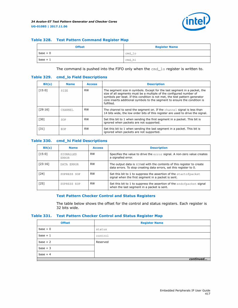
Table 328. Test Pattern Command Register Map
Offset Register Name
base + 0 cmd_lo
base + 1 cmd_hi
The command is pushed into the FIFO only when the cmd_lo register is written to.
Table 329. cmd_lo Field Descriptions
Bit(s) Name Access Description
[15:0] SIZE RW The segment size in symbols. Except for the last segment in a packet, thesize of all segments must be a multiple of the configured number ofsymbols per beat. If this condition is not met, the test pattern generatorcore inserts additional symbols to the segment to ensure the condition isfulfilled.
[29:16] CHANNEL RW The channel to send the segment on. If the channel signal is less than14 bits wide, the low order bits of this register are used to drive the signal.
[30] SOP RW Set this bit to 1 when sending the first segment in a packet. This bit isignored when packets are not supported.
[31] EOP RW Set this bit to 1 when sending the last segment in a packet. This bit isignored when packets are not supported.
Table 330. cmd_hi Field Descriptions
Bit(s) Name Access Description
[15:0] SIGNALLEDERROR
RW Specifies the value to drive the error signal. A non-zero value createsa signalled error.
[23:16] DATA ERROR RW The output data is XORed with the contents of this register to createdata errors. To stop creating data errors, set this register to 0.
[24] SUPRESS SOP RW Set this bit to 1 to suppress the assertion of the startofpacketsignal when the first segment in a packet is sent.
[25] SUPRESS EOP RW Set this bit to 1 to suppress the assertion of the endofpacket signalwhen the last segment in a packet is sent.
Test Pattern Checker Control and Status Registers
The table below shows the offset for the control and status registers. Each register is32 bits wide.
Table 331. Test Pattern Checker Control and Status Register Map
Offset Register Name
base + 0 status
base + 1 control
base + 2 Reserved
base + 3
base + 4
continued...
34 Avalon-ST Test Pattern Generator and Checker Cores
UG-01085 | 2017.11.06
Embedded Peripherals IP User Guide417
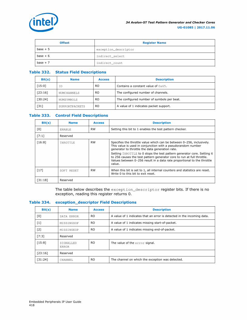
Offset Register Name
base + 5 exception_descriptor
base + 6 indirect_select
base + 7 indirect_count
Table 332. Status Field Descriptions
Bit(s) Name Access Description
[15:0] ID RO Contains a constant value of 0x65.
[23:16] NUMCHANNELS RO The configured number of channels.
[30:24] NUMSYMBOLS RO The configured number of symbols per beat.
[31] SUPPORTPACKETS RO A value of 1 indicates packet support.
Table 333. Control Field Descriptions
Bit(s) Name Access Description
[0] ENABLE RW Setting this bit to 1 enables the test pattern checker.
[7:1] Reserved
[16:8] THROTTLE RW Specifies the throttle value which can be between 0–256, inclusively.This value is used in conjunction with a pseudorandom numbergenerator to throttle the data generation rate.Setting THROTTLE to 0 stops the test pattern generator core. Setting itto 256 causes the test pattern generator core to run at full throttle.Values between 0–256 result in a data rate proportional to the throttlevalue.
[17] SOFT RESET RW When this bit is set to 1, all internal counters and statistics are reset.Write 0 to this bit to exit reset.
[31:18] Reserved
The table below describes the exception_descriptor register bits. If there is noexception, reading this register returns 0.
Table 334. exception_descriptor Field Descriptions
Bit(s) Name Access Description
[0] DATA ERROR RO A value of 1 indicates that an error is detected in the incoming data.
[1] MISSINGSOP RO A value of 1 indicates missing start-of-packet.
[2] MISSINGEOP RO A value of 1 indicates missing end-of-packet.
[7:3] Reserved
[15:8] SIGNALLEDERROR
RO The value of the error signal.
[23:16] Reserved
[31:24] CHANNEL RO The channel on which the exception was detected.
34 Avalon-ST Test Pattern Generator and Checker Cores
UG-01085 | 2017.11.06
Embedded Peripherals IP User Guide418
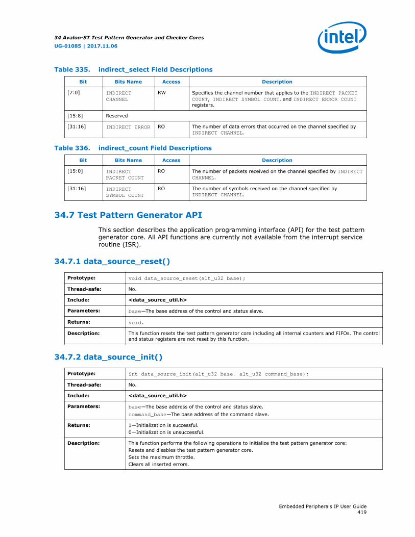
Table 335. indirect_select Field Descriptions
Bit Bits Name Access Description
[7:0] INDIRECTCHANNEL
RW Specifies the channel number that applies to the INDIRECT PACKETCOUNT, INDIRECT SYMBOL COUNT, and INDIRECT ERROR COUNTregisters.
[15:8] Reserved
[31:16] INDIRECT ERROR RO The number of data errors that occurred on the channel specified byINDIRECT CHANNEL.
Table 336. indirect_count Field Descriptions
Bit Bits Name Access Description
[15:0] INDIRECTPACKET COUNT
RO The number of packets received on the channel specified by INDIRECTCHANNEL.
[31:16] INDIRECTSYMBOL COUNT
RO The number of symbols received on the channel specified byINDIRECT CHANNEL.
34.7 Test Pattern Generator API
This section describes the application programming interface (API) for the test patterngenerator core. All API functions are currently not available from the interrupt serviceroutine (ISR).
34.7.1 data_source_reset()
Prototype: void data_source_reset(alt_u32 base);
Thread-safe: No.
Include: <data_source_util.h>
Parameters: base—The base address of the control and status slave.
Returns: void.
Description: This function resets the test pattern generator core including all internal counters and FIFOs. The controland status registers are not reset by this function.
34.7.2 data_source_init()
Prototype: int data_source_init(alt_u32 base, alt_u32 command_base);
Thread-safe: No.
Include: <data_source_util.h>
Parameters: base—The base address of the control and status slave.command_base—The base address of the command slave.
Returns: 1—Initialization is successful.0—Initialization is unsuccessful.
Description: This function performs the following operations to initialize the test pattern generator core:Resets and disables the test pattern generator core.Sets the maximum throttle.Clears all inserted errors.
34 Avalon-ST Test Pattern Generator and Checker Cores
UG-01085 | 2017.11.06
Embedded Peripherals IP User Guide419

34.7.3 data_source_get_id()
Prototype: int data_source_get_id(alt_u32 base);
Thread-safe: Yes.
Include: <data_source_util.h>
Parameters: base—The base address of the control and status slave.
Returns: The test pattern generator core’s identifier.
Description: This function retrieves the test pattern generator core’s identifier.
34.7.4 data_source_get_supports_packets()
Prototype: int data_source_init(alt_u32 base);
Thread-safe: Yes.
Include: <data_source_util.h>
Parameters: base—The base address of the control and status slave.
Returns: 1—Packets are supported.0—Packets are not supported.
Description: This function checks if the test pattern generator core supports packets.
34.7.5 data_source_get_num_channels()
Prototype: int data_source_get_num_channels(alt_u32 base);
Thread-safe: Yes.
Include: <data_source_util.h>
Parameters: base—The base address of the control and status slave.
Returns: The number of channels supported.
Description: This function retrieves the number of channels supported by the test pattern generator core.
34.7.6 data_source_get_symbols_per_cycle()
Prototype: int data_source_get_symbols(alt_u32 base);
Thread-safe: Yes.
Include: <data_source_util.h>
Parameters: base—The base address of the control and status slave.
Returns: The number of symbols transferred in a beat.
Description: This function retrieves the number of symbols transferred by the test pattern generator core in eachbeat.
34 Avalon-ST Test Pattern Generator and Checker Cores
UG-01085 | 2017.11.06
Embedded Peripherals IP User Guide420

34.7.7 data_source_set_enable()
Prototype: void data_source_set_enable(alt_u32 base, alt_u32 value);
Thread-safe: No.
Include: <data_source_util.h>
Parameters: base—The base address of the control and status slave.value—The ENABLE bit is set to the value of this parameter.
Returns: void.
Description: This function enables or disables the test pattern generator core. When disabled, the test patterngenerator core stops data transmission but continues to accept commands and stores them in the FIFO.
34.7.8 data_source_get_enable()
Prototype: int data_source_get_enable(alt_u32 base);
Thread-safe: Yes.
Include: <data_source_util.h>
Parameters: base—The base address of the control and status slave.
Returns: The value of the ENABLE bit.
Description: This function retrieves the value of the ENABLE bit.
34.7.9 data_source_set_throttle()
Prototype: void data_source_set_throttle(alt_u32 base, alt_u32 value);
Thread-safe: No.
Include: <data_source_util.h>
Parameters: base—The base address of the control and status slave.value—The throttle value.
Returns: void.
Description: This function sets the throttle value, which can be between 0–256 inclusively. The throttle value, whendivided by 256 yields the rate at which the test pattern generator sends data.
34.7.10 data_source_get_throttle()
Prototype: int data_source_get_throttle(alt_u32 base);
Thread-safe: Yes.
Include: <data_source_util.h>
Parameters: base—The base address of the control and status slave.
Returns: The throttle value.
Description: This function retrieves the current throttle value.
34 Avalon-ST Test Pattern Generator and Checker Cores
UG-01085 | 2017.11.06
Embedded Peripherals IP User Guide421

34.7.11 data_source_is_busy()
Prototype: int data_source_is_busy(alt_u32 base);
Thread-safe: Yes.
Include: <data_source_util.h>
Parameters: base—The base address of the control and status slave.
Returns: 1—The test pattern generator core is busy.0—The core is not busy.
Description: This function checks if the test pattern generator is busy. The test pattern generator core is busy when itis sending data or has data in the command FIFO to be sent.
34.7.12 data_source_fill_level()
Prototype: int data_source_fill_level(alt_u32 base);
Thread-safe: Yes.
Include: <data_source_util.h>
Parameters: base—The base address of the control and status slave.
Returns: The number of commands in the command FIFO.
Description: This function retrieves the number of commands currently in the command FIFO.
34.7.13 data_source_send_data()
Prototype: int data_source_send_data(alt_u32 cmd_base, alt_u16 channel, alt_u16 size,alt_u32 flags, alt_u16 error, alt_u8 data_error_mask);
Thread-safe: No.
Include: <data_source_util.h>
Parameters: cmd_base—The base address of the command slave.channel—The channel to send the data on.size—The data size.flags—Specifies whether to send or suppress SOP and EOP signals. Valid values areDATA_SOURCE_SEND_SOP, DATA_SOURCE_SEND_EOP, DATA_SOURCE_SEND_SUPRESS_SOP andDATA_SOURCE_SEND_SUPRESS_EOP.error—The value asserted on the error signal on the output interface.data_error_mask—This parameter and the data are XORed together to produce erroneous data.
Returns: Always returns 1.
Description: This function sends a data fragment to the specified channel.If packets are supported, user applications must ensure the following conditions are met:SOP and EOP are used consistently in each channel.Except for the last segment in a packet, the length of each segment is a multiple of the data width.If packets are not supported, user applications must ensure the following conditions are met:No SOP and EOP indicators in the data.The length of each segment in a packet is a multiple of the data width.
34 Avalon-ST Test Pattern Generator and Checker Cores
UG-01085 | 2017.11.06
Embedded Peripherals IP User Guide422

34.8 Test Pattern Checker API
This section describes the API for the test pattern checker core. The API functions arecurrently not available from the ISR.
34.8.1 data_sink_reset()
Prototype: void data_sink_reset(alt_u32 base);
Thread-safe: No.
Include: <data_sink_util.h>
Parameters: base—The base address of the control and status slave.
Returns: void.
Description: This function resets the test pattern checker core including all internal counters.
34.8.2 data_sink_init()
Prototype: int data_source_init(alt_u32 base);
Thread-safe: No.
Include: <data_sink_util.h>
Parameters: base—The base address of the control and status slave.
Returns: 1—Initialization is successful.0—Initialization is unsuccessful.
Description: This function performs the following operations to initialize the test pattern checker core:Resets and disables the test pattern checker core.Sets the throttle to the maximum value.
34.8.3 data_sink_get_id()
Prototype: int data_sink_get_id(alt_u32 base);
Thread-safe: Yes.
Include: <data_sink_util.h>
Parameters: base—The base address of the control and status slave.
Returns: The test pattern checker core’s identifier.
Description: This function retrieves the test pattern checker core’s identifier.
34.8.4 data_sink_get_supports_packets()
Prototype: int data_sink_init(alt_u32 base);
Thread-safe: Yes.
Include: <data_sink_util.h>
Parameters: base—The base address of the control and status slave.
Returns: 1—Packets are supported.
continued...
34 Avalon-ST Test Pattern Generator and Checker Cores
UG-01085 | 2017.11.06
Embedded Peripherals IP User Guide423

0—Packets are not supported.
Description: This function checks if the test pattern checker core supports packets.
34.8.5 data_sink_get_num_channels()
Prototype: int data_sink_get_num_channels(alt_u32 base);
Thread-safe: Yes.
Include: <data_sink_util.h>
Parameters: base—The base address of the control and status slave.
Returns: The number of channels supported.
Description: This function retrieves the number of channels supported by the test pattern checker core.
34.8.6 data_sink_get_symbols_per_cycle()
Prototype: int data_sink_get_symbols(alt_u32 base);
Thread-safe: Yes.
Include: <data_sink_util.h>
Parameters: base—The base address of the control and status slave.
Returns: The number of symbols received in a beat.
Description: This function retrieves the number of symbols received by the test pattern checker core in each beat.
34.8.7 data_sink_set enable()
Prototype: void data_sink_set_enable(alt_u32 base, alt_u32 value);
Thread-safe: No.
Include: <data_sink_util.h>
Parameters: base—The base address of the control and status slave.value—The ENABLE bit is set to the value of this parameter.
Returns: void.
Description: This function enables the test pattern checker core.
34.8.8 data_sink_get_enable()
Prototype: int data_sink_get_enable(alt_u32 base);
Thread-safe: Yes.
Include: <data_sink_util.h>
Parameters: base—The base address of the control and status slave.
Returns: The value of the ENABLE bit.
Description: This function retrieves the value of the ENABLE bit.
34 Avalon-ST Test Pattern Generator and Checker Cores
UG-01085 | 2017.11.06
Embedded Peripherals IP User Guide424
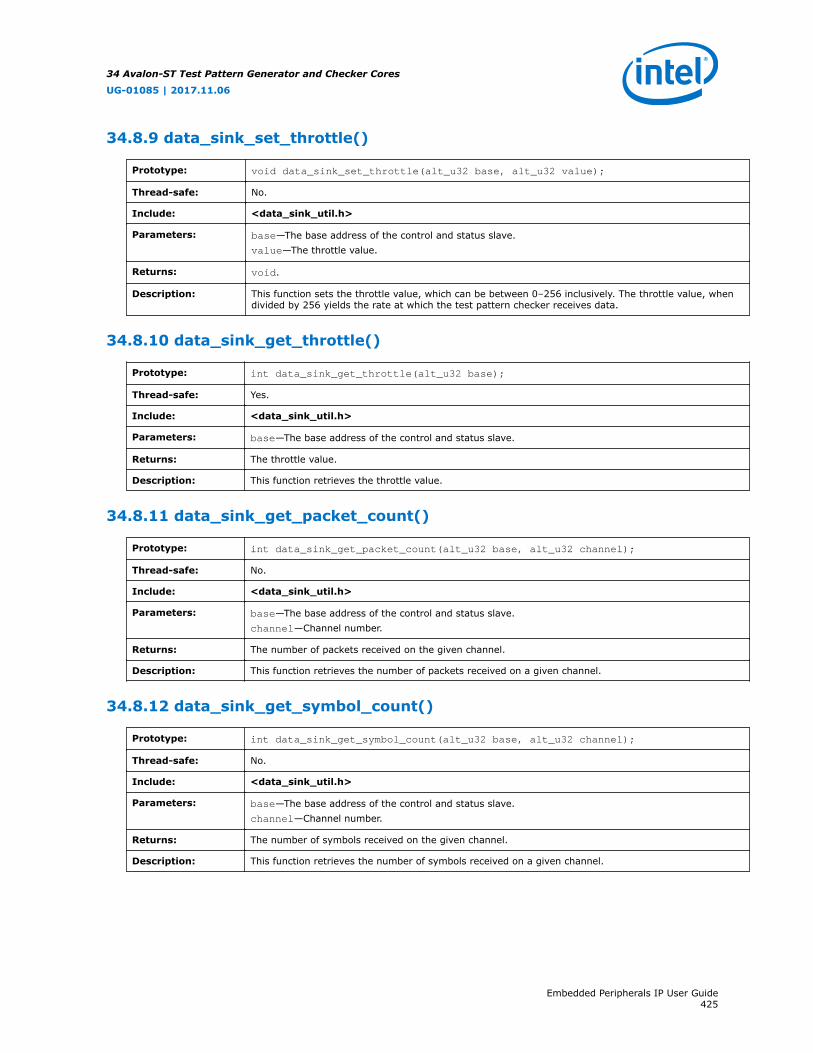
34.8.9 data_sink_set_throttle()
Prototype: void data_sink_set_throttle(alt_u32 base, alt_u32 value);
Thread-safe: No.
Include: <data_sink_util.h>
Parameters: base—The base address of the control and status slave.value—The throttle value.
Returns: void.
Description: This function sets the throttle value, which can be between 0–256 inclusively. The throttle value, whendivided by 256 yields the rate at which the test pattern checker receives data.
34.8.10 data_sink_get_throttle()
Prototype: int data_sink_get_throttle(alt_u32 base);
Thread-safe: Yes.
Include: <data_sink_util.h>
Parameters: base—The base address of the control and status slave.
Returns: The throttle value.
Description: This function retrieves the throttle value.
34.8.11 data_sink_get_packet_count()
Prototype: int data_sink_get_packet_count(alt_u32 base, alt_u32 channel);
Thread-safe: No.
Include: <data_sink_util.h>
Parameters: base—The base address of the control and status slave.channel—Channel number.
Returns: The number of packets received on the given channel.
Description: This function retrieves the number of packets received on a given channel.
34.8.12 data_sink_get_symbol_count()
Prototype: int data_sink_get_symbol_count(alt_u32 base, alt_u32 channel);
Thread-safe: No.
Include: <data_sink_util.h>
Parameters: base—The base address of the control and status slave.channel—Channel number.
Returns: The number of symbols received on the given channel.
Description: This function retrieves the number of symbols received on a given channel.
34 Avalon-ST Test Pattern Generator and Checker Cores
UG-01085 | 2017.11.06
Embedded Peripherals IP User Guide425
34.8.13 data_sink_get_error_count()
Prototype: int data_sink_get_error_count(alt_u32 base, alt_u32 channel);
Thread-safe: No.
Include: <data_sink_util.h>
Parameters: base—The base address of the control and status slave.channel—Channel number.
Returns: The number of errors received on the given channel.
Description: This function retrieves the number of errors received on a given channel.
34.8.14 data_sink_get_exception()
Prototype: int data_sink_get_exception(alt_u32 base);
Thread-safe: Yes.
Include: <data_sink_util.h>
Parameters: base—The base address of the control and status slave.
Returns: The first exception descriptor in the exception FIFO.0—No exception descriptor found in the exception FIFO.
Description: This function retrieves the first exception descriptor in the exception FIFO and pops it off the FIFO.
34.8.15 data_sink_exception_is_exception()
Prototype: int data_sink_exception_is_exception(int exception);
Thread-safe: Yes.
Include: <data_sink_util.h>
Parameters: exception—Exception descriptor
Returns: 1—Indicates an exception.0—No exception.
Description: This function checks if a given exception descriptor describes a valid exception.
34.8.16 data_sink_exception_has_data_error()
Prototype: int data_sink_exception_has_data_error(int exception);
Thread-safe: Yes.
Include: <data_sink_util.h>
Parameters: exception—Exception descriptor.
Returns: 1—Data has errors.0—No errors.
Description: This function checks if a given exception indicates erroneous data.
34 Avalon-ST Test Pattern Generator and Checker Cores
UG-01085 | 2017.11.06
Embedded Peripherals IP User Guide426
34.8.17 data_sink_exception_has_missing_sop()
Prototype: int data_sink_exception_has_missing_sop(int exception);
Thread-safe: Yes.
Include: <data_sink_util.h>
Parameters: exception—Exception descriptor.
Returns: 1—Missing SOP.0—Other exception types.
Description: This function checks if a given exception descriptor indicates missing SOP.
34.8.18 data_sink_exception_has_missing_eop()
Prototype: int data_sink_exception_has_missing_eop(int exception);
Thread-safe: Yes.
Include: <data_sink_util.h>
Parameters: exception—Exception descriptor.
Returns: 1—Missing EOP.0—Other exception types.
Description: This function checks if a given exception descriptor indicates missing EOP.
34.8.19 data_sink_exception_signalled_error()
Prototype: int data_sink_exception_signalled_error(int exception);
Thread-safe: Yes.
Include: <data_sink_util.h>
Parameters: exception—Exception descriptor.
Returns: The signalled error value.
Description: This function retrieves the value of the signalled error from the exception.
34.8.20 data_sink_exception_channel()
Prototype: int data_sink_exception_channel(int exception);
Thread-safe: Yes.
Include: <data_sink_util.h>
Parameters: exception—Exception descriptor.
Returns: The channel number on which the given exception occurred.
Description: This function retrieves the channel number on which a given exception occurred.
34 Avalon-ST Test Pattern Generator and Checker Cores
UG-01085 | 2017.11.06
Embedded Peripherals IP User Guide427

34.9 Document Revision History
Table 337. Avalon Streaming Test Pattern Generator and Checker Cores Revision History
Date Version Changes
December 2010 v10.1.0 Removed the “Device Support”, “Instantiating the Core in SOPC Builder”,and “Referenced Documents” sections.
July 2010 v10.0.0 No change from previous release.
November 2009 v9.1.0 No change from previous release.
March 2009 v9.0.0 No change from previous release.
November 2008 v8.1.0 Changed to 8-1/2 x 11 page size. No change to content.
May 2008 v8.0.0 Updated the section on HAL System Library Support.
34 Avalon-ST Test Pattern Generator and Checker Cores
UG-01085 | 2017.11.06
Embedded Peripherals IP User Guide428
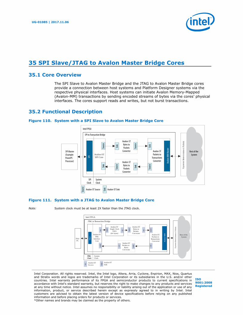
35 SPI Slave/JTAG to Avalon Master Bridge Cores
35.1 Core Overview
The SPI Slave to Avalon Master Bridge and the JTAG to Avalon Master Bridge coresprovide a connection between host systems and Platform Designer systems via therespective physical interfaces. Host systems can initiate Avalon Memory-Mapped(Avalon-MM) transactions by sending encoded streams of bytes via the cores’ physicalinterfaces. The cores support reads and writes, but not burst transactions.
35.2 Functional Description
Figure 110. System with a SPI Slave to Avalon Master Bridge Core
aF tcennocretnI
metsyS
bcir
Avalon-STSPI Core
Intel FPGA
SPI to Transaction Bridge
SPIClock
SystemClock
SPI Master(Example:PowerPCProcessor)
Avalon-STBytes toPackets
Converter
Avalon-STBytes toPackets
Converter
Avalon-STPackets to
TransactionsConverter
Rest of the System
Avalo
n-M
M M
aste
r
SPI
Sink
Sour
ce
Sink
Sink
Sink
Sour
ce
Sour
ce
Sour
ce
Sink
Sour
ce
Avalon-ST Source Avalon-ST Sink
Figure 111. System with a JTAG to Avalon Master Bridge Core
Note: System clock must be at least 2X faster than the JTAG clock.
aF tcennocretnI
metsyS
bcir
Rest of the System
HostPC
JTAG to Transaction Bridge
srckn
i s
Avalon-STBytes toPackets
Con verter
srckn
i s
Avalon-STPackets to
TransactionsCon verter A
valo
n-M
M
src Avalon-ST
So urce sink
Avalon-STSink
srckn
i s
Avalon-ST
FIFO(64 bytes)
src knis
Avalon-STPackets to
BytesCon verter
Avalon-STJTAG
InterfaceCore
GATJ
src
knis
JTAGClockJTAGClock
SystemClock
Intel FPGA
Single Clock
UG-01085 | 2017.11.06
Intel Corporation. All rights reserved. Intel, the Intel logo, Altera, Arria, Cyclone, Enpirion, MAX, Nios, Quartusand Stratix words and logos are trademarks of Intel Corporation or its subsidiaries in the U.S. and/or othercountries. Intel warrants performance of its FPGA and semiconductor products to current specifications inaccordance with Intel's standard warranty, but reserves the right to make changes to any products and servicesat any time without notice. Intel assumes no responsibility or liability arising out of the application or use of anyinformation, product, or service described herein except as expressly agreed to in writing by Intel. Intelcustomers are advised to obtain the latest version of device specifications before relying on any publishedinformation and before placing orders for products or services.*Other names and brands may be claimed as the property of others.
ISO9001:2008Registered
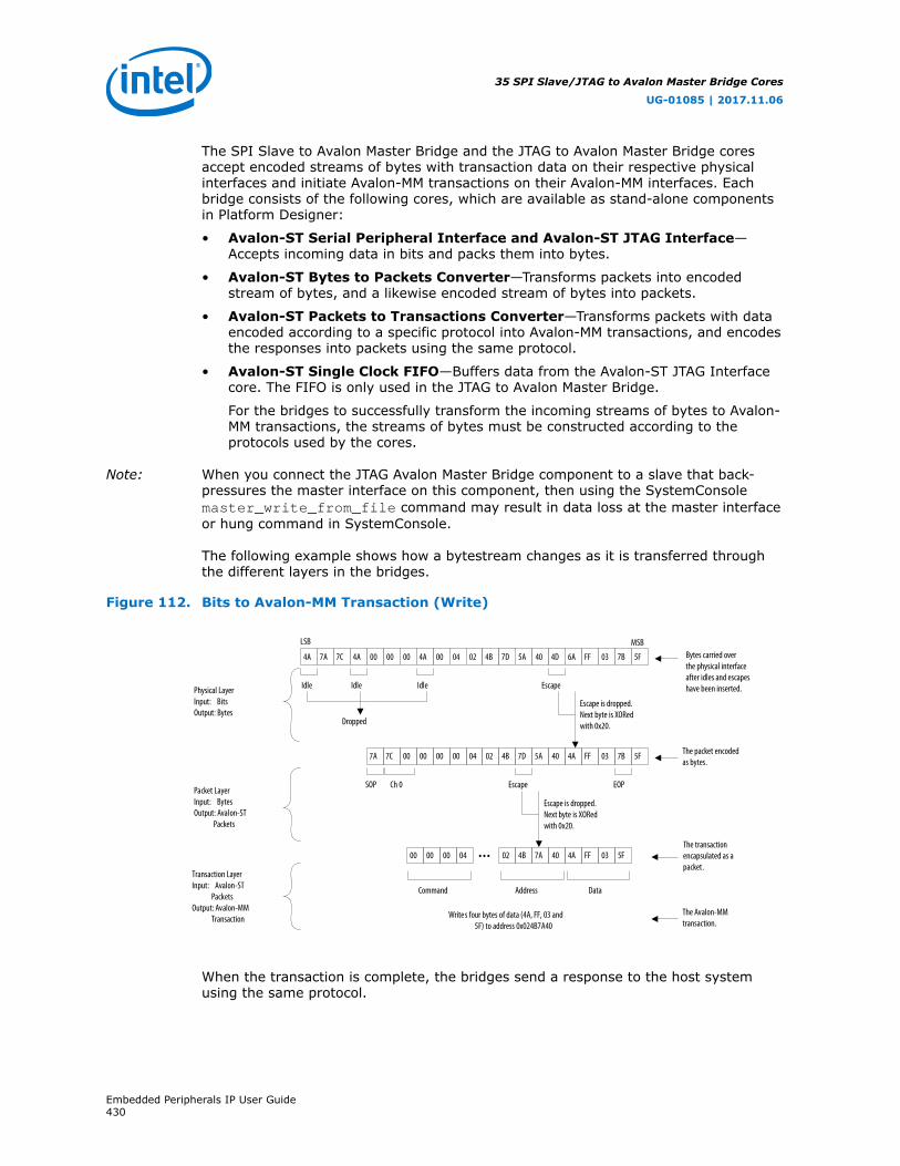
The SPI Slave to Avalon Master Bridge and the JTAG to Avalon Master Bridge coresaccept encoded streams of bytes with transaction data on their respective physicalinterfaces and initiate Avalon-MM transactions on their Avalon-MM interfaces. Eachbridge consists of the following cores, which are available as stand-alone componentsin Platform Designer:
• Avalon-ST Serial Peripheral Interface and Avalon-ST JTAG Interface—Accepts incoming data in bits and packs them into bytes.
• Avalon-ST Bytes to Packets Converter—Transforms packets into encodedstream of bytes, and a likewise encoded stream of bytes into packets.
• Avalon-ST Packets to Transactions Converter—Transforms packets with dataencoded according to a specific protocol into Avalon-MM transactions, and encodesthe responses into packets using the same protocol.
• Avalon-ST Single Clock FIFO—Buffers data from the Avalon-ST JTAG Interfacecore. The FIFO is only used in the JTAG to Avalon Master Bridge.
For the bridges to successfully transform the incoming streams of bytes to Avalon-MM transactions, the streams of bytes must be constructed according to theprotocols used by the cores.
Note: When you connect the JTAG Avalon Master Bridge component to a slave that back-pressures the master interface on this component, then using the SystemConsolemaster_write_from_file command may result in data loss at the master interfaceor hung command in SystemConsole.
The following example shows how a bytestream changes as it is transferred throughthe different layers in the bridges.
Figure 112. Bits to Avalon-MM Transaction (Write)
00 00 00 047A 7C 00 02 4B 5A 407D 6A FF 03 5F7B4A 4A 4A 4D
00 00 00 04 02 4B 7A 40 4A FF 03 5F
Command Address Data
Writes four bytes of data (4A, FF, 03 and 5F) to address 0x024B7A40
Packet LayerInput: BytesOutput: Avalon-ST Packets
Transaction LayerInput: Avalon-ST PacketsOutput: Avalon-MM Transaction
00 00 00 047A 7C 00 02 4B 5A 407D 4A FF 03 5F7B
LSB MSB
Idle Idle Idle Escape
Dropped
Escape is dropped. Next byte is XORed with 0x20.
Physical LayerInput: BitsOutput: Bytes
SOP Ch 0 Escape
Escape is dropped.Next byte is XORed with 0x20.
EOP
Bytes carried overthe physical interfaceafter idles and escapes have been inserted.
The packet encoded as bytes.
The transaction encapsulated as a packet.
The Avalon-MMtransaction.
...
When the transaction is complete, the bridges send a response to the host systemusing the same protocol.
35 SPI Slave/JTAG to Avalon Master Bridge Cores
UG-01085 | 2017.11.06
Embedded Peripherals IP User Guide430

Figure 113. Bits to Avalon-MM Transaction (Read)
00 00 00 047A 7C 00 02 4B 5A 407D 6A FF 03 5F7B4A 4A 4A 4D
10 00 00 04 02 4B 7A 40 4A FF 03 5F
Command Address Data
Reads four bytes of data (4A, FF, 03 and 5F) to address 0x024B7A40
Packet LayerInput: BytesOutput: Avalon-ST Packets
Transaction LayerInput: Avalon-ST PacketsOutput: Avalon-MM Transaction
00 00 00 047A 7C 00 02 4B 5A 407D 4A FF 03 5F7B
LSB MSB
Idle Idle Idle Escape
Dropped
Escape is dropped. Next byte is XORed with 0x20.
Physical LayerInput: BitsOutput: Bytes
SOP Ch 0 Escape
Escape is dropped.Next byte is XORed with 0x20.
EOP
Bytes carried overthe physical interfaceafter idles and escapes have been inserted.
The packet encoded as bytes.
The transaction encapsulated as a packet.
The Avalon-MMtransaction.
...
Related Links
• Avalon-ST Serial Peripheral Interface Core on page 32
• Avalon-ST Bytes to Packets and Packets to Bytes Converter Cores on page 447
• Avalon Packets to Transactions Converter Core on page 436
• Avalon-ST Single-Clock and Dual-Clock FIFO Cores on page 26
35.3 Parameters
For the SPI Slave to Avalon Master Bridge core, the parameter Number ofsynchronizer stages: Depth allows you to specify the length of synchronizationregister chains. These register chains are used when a metastable event is likely tooccur and the length specified determines the meantime before failure. The registerchain length, however, affects the latency of the core.
For more information on metastability in Intel FPGA devices, refer to AN 42:Metastability in Intel FPGA devices.
For more information on metastability analysis and synchronization register chains,refer to the Area and Timing Optimization chapter in volume 2 of the Intel QuartusPrime Handbook.
35 SPI Slave/JTAG to Avalon Master Bridge Cores
UG-01085 | 2017.11.06
Embedded Peripherals IP User Guide431
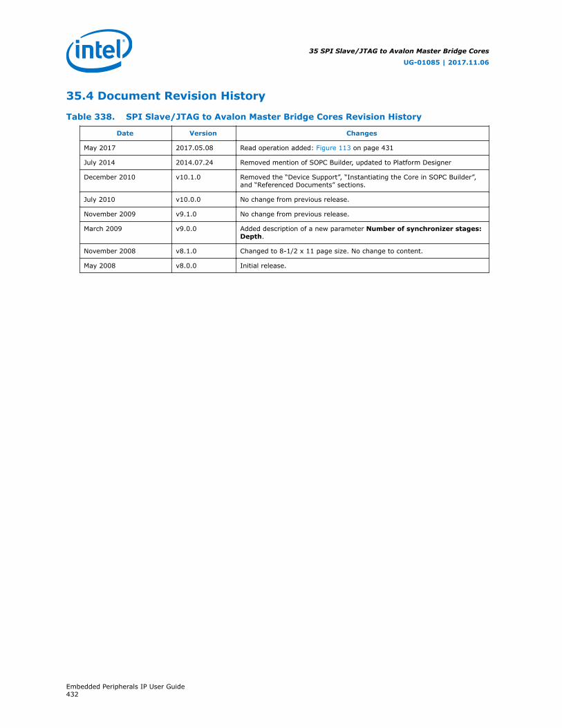
35.4 Document Revision History
Table 338. SPI Slave/JTAG to Avalon Master Bridge Cores Revision History
Date Version Changes
May 2017 2017.05.08 Read operation added: Figure 113 on page 431
July 2014 2014.07.24 Removed mention of SOPC Builder, updated to Platform Designer
December 2010 v10.1.0 Removed the “Device Support”, “Instantiating the Core in SOPC Builder”,and “Referenced Documents” sections.
July 2010 v10.0.0 No change from previous release.
November 2009 v9.1.0 No change from previous release.
March 2009 v9.0.0 Added description of a new parameter Number of synchronizer stages:Depth.
November 2008 v8.1.0 Changed to 8-1/2 x 11 page size. No change to content.
May 2008 v8.0.0 Initial release.
35 SPI Slave/JTAG to Avalon Master Bridge Cores
UG-01085 | 2017.11.06
Embedded Peripherals IP User Guide432
36 System ID Peripheral Core
36.1 Core Overview
The system ID core with Avalon interface is a simple read-only device that providesPlatform Designer systems with a unique identifier. Nios II processor systems use thesystem ID core to verify that an executable program was compiled targeting theactual hardware image configured in the target FPGA. If the expected ID in theexecutable does not match the system ID core in the FPGA, it is possible that thesoftware will not execute correctly.
36.2 Functional Description
The system ID core provides a read-only Avalon Memory-Mapped (Avalon-MM) slaveinterface. This interface has two 32-bit registers, as shown in the table below. Thevalue of each register is determined at system generation time, and always returns aconstant value.
Table 339. System ID Core Register Map
Offset Register Name R/W Description
0 id R A unique 32-bit value that is based on the contents of thePlatform Designer system. The id is similar to a check-sumvalue; Platform Designer systems with differentcomponents, different configuration options, or both,produce different id values.
1 timestamp R A unique 32-bit value that is based on the systemgeneration time. The value is equivalent to the number ofseconds after Jan. 1, 1970.
There are two basic ways to use the system ID core:
• Verify the system ID before downloading new software to a system. This methodis used by software development tools, such as the Nios II integrated developmentenvironment (IDE). There is little point in downloading a program to a targethardware system, if the program is compiled for different hardware. Therefore, theNios II IDE checks that the system ID core in hardware matches the expectedsystem ID of the software before downloading a program to run or debug.
• Check system ID after reset. If a program is running on hardware other than theexpected Platform Designer system, the program may fail to function altogether. Ifthe program does not crash, it can behave erroneously in subtle ways that aredifficult to debug. To protect against this case, a program can compare theexpected system ID against the system ID core, and report an error if they do notmatch.
UG-01085 | 2017.11.06
Intel Corporation. All rights reserved. Intel, the Intel logo, Altera, Arria, Cyclone, Enpirion, MAX, Nios, Quartusand Stratix words and logos are trademarks of Intel Corporation or its subsidiaries in the U.S. and/or othercountries. Intel warrants performance of its FPGA and semiconductor products to current specifications inaccordance with Intel's standard warranty, but reserves the right to make changes to any products and servicesat any time without notice. Intel assumes no responsibility or liability arising out of the application or use of anyinformation, product, or service described herein except as expressly agreed to in writing by Intel. Intelcustomers are advised to obtain the latest version of device specifications before relying on any publishedinformation and before placing orders for products or services.*Other names and brands may be claimed as the property of others.
ISO9001:2008Registered

36.3 Configuration
The id and timestamp register values are determined at system generation timebased on the configuration of the Platform Designer system and the current time. Youcan add only one system ID core to an Platform Designer system, and its name isalways sysid.
After system generation, you can examine the values stored in the id andtimestamp registers by opening the MegaWizard interface for the System ID core.
Since a unique timestamp value is added to the System ID HDL file each time yougenerate the Platform Designer system, the Intel Quartus Prime software recompilesthe entire system if you have added the system as a design partition.
Note: In Intel Quartus Prime Pro Edition 17.1, the Platform Designer generation processneeds an additional TCL script for manual execution to have a unique timestampvalue.
Follow these steps to have a unique timestamp value using the Intel Quartus PrimePro Edition 17.1 version:
1. Create a Platform Designer system with the System ID core.
2. Go to View>System Scripting. Click on User Scripts and direct to soceds/examples/hardware/<*_ghrd folder>/update_sysid.tcl (you may alsocopy the script into your local directory and point to it).
3. Click on Run Script.
4. After you run the script, the IP Parameter Editor window appears. Ensure that nomessage is shown under System Scripting.
5. Save changes to your .ip file and change the variant to .qsys file.
6. Click on Sync System Info in Platform Designer.
7. Click on Generate HDL.
36.4 Software Programming Model
This section describes the software programming model for the system ID core. ForNios II processor users, Intel provides the HAL system library header file that definesthe System ID core registers.
The System ID core comes with the following software files. These files provide low-level access to the hardware. Application developers should not modify these files.
• alt_avalon_sysid_regs.h—Defines the interface to the hardware registers.
• alt_avalon_sysid.c, alt_avalon_sysid.h—Header and source filesdefining the hardware access functions.
Intel provides one access routine, alt_avalon_sysid_test(), that returns avalue indicating whether the system ID expected by software matches the systemID core.
36 System ID Peripheral Core
UG-01085 | 2017.11.06
Embedded Peripherals IP User Guide434
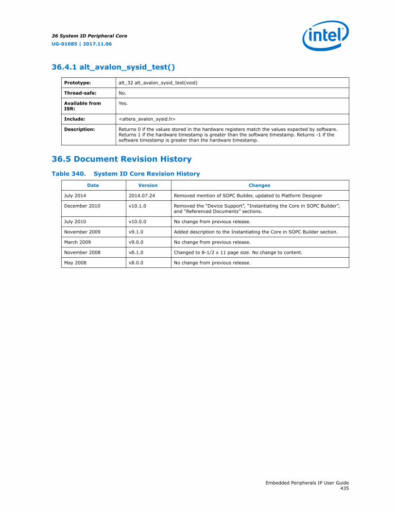
36.4.1 alt_avalon_sysid_test()
Prototype: alt_32 alt_avalon_sysid_test(void)
Thread-safe: No.
Available fromISR:
Yes.
Include: <altera_avalon_sysid.h>
Description: Returns 0 if the values stored in the hardware registers match the values expected by software.Returns 1 if the hardware timestamp is greater than the software timestamp. Returns -1 if thesoftware timestamp is greater than the hardware timestamp.
36.5 Document Revision History
Table 340. System ID Core Revision History
Date Version Changes
July 2014 2014.07.24 Removed mention of SOPC Builder, updated to Platform Designer
December 2010 v10.1.0 Removed the “Device Support”, “Instantiating the Core in SOPC Builder”,and “Referenced Documents” sections.
July 2010 v10.0.0 No change from previous release.
November 2009 v9.1.0 Added description to the Instantiating the Core in SOPC Builder section.
March 2009 v9.0.0 No change from previous release.
November 2008 v8.1.0 Changed to 8-1/2 x 11 page size. No change to content.
May 2008 v8.0.0 No change from previous release.
36 System ID Peripheral Core
UG-01085 | 2017.11.06
Embedded Peripherals IP User Guide435
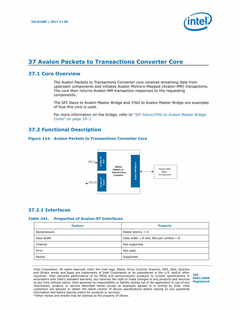
37 Avalon Packets to Transactions Converter Core
37.1 Core Overview
The Avalon Packets to Transactions Converter core receives streaming data fromupstream components and initiates Avalon Memory-Mapped (Avalon-MM) transactions.The core then returns Avalon-MM transaction responses to the requestingcomponents.
The SPI Slave to Avalon Master Bridge and JTAG to Avalon Master Bridge are examplesof how this core is used.
For more information on the bridge, refer to “SPI Slave/JTAG to Avalon Master BridgeCores” on page 18–1
37.2 Functional Description
Figure 114. Avalon Packets to Transactions Converter Core
Ava
lon-
ST
Sink
Avalon Packets to
TransactionsConverter
data_out
rets aM
MM-nol avA
data_in
Ava
lon-
ST
Sour
ce
Avalon-MMSlave
Component
37.2.1 Interfaces
Table 341. Properties of Avalon-ST Interfaces
Feature Property
Backpressure Ready latency = 0.
Data Width Data width = 8 bits; Bits per symbol = 8.
Channel Not supported.
Error Not used.
Packet Supported.
UG-01085 | 2017.11.06
Intel Corporation. All rights reserved. Intel, the Intel logo, Altera, Arria, Cyclone, Enpirion, MAX, Nios, Quartusand Stratix words and logos are trademarks of Intel Corporation or its subsidiaries in the U.S. and/or othercountries. Intel warrants performance of its FPGA and semiconductor products to current specifications inaccordance with Intel's standard warranty, but reserves the right to make changes to any products and servicesat any time without notice. Intel assumes no responsibility or liability arising out of the application or use of anyinformation, product, or service described herein except as expressly agreed to in writing by Intel. Intelcustomers are advised to obtain the latest version of device specifications before relying on any publishedinformation and before placing orders for products or services.*Other names and brands may be claimed as the property of others.
ISO9001:2008Registered
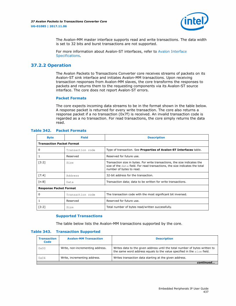
The Avalon-MM master interface supports read and write transactions. The data widthis set to 32 bits and burst transactions are not supported.
For more information about Avalon-ST interfaces, refer to Avalon InterfaceSpecifications.
37.2.2 Operation
The Avalon Packets to Transactions Converter core receives streams of packets on itsAvalon-ST sink interface and initiates Avalon-MM transactions. Upon receivingtransaction responses from Avalon-MM slaves, the core transforms the responses topackets and returns them to the requesting components via its Avalon-ST sourceinterface. The core does not report Avalon-ST errors.
Packet Formats
The core expects incoming data streams to be in the format shown in the table below.A response packet is returned for every write transaction. The core also returns aresponse packet if a no transaction (0x7f) is received. An invalid transaction code isregarded as a no transaction. For read transactions, the core simply returns the dataread.
Table 342. Packet Formats
Byte Field Description
Transaction Packet Format
0 Transaction code Type of transaction. See Properties of Avalon-ST Interfaces table.
1 Reserved Reserved for future use.
[3:2] Size Transaction size in bytes. For write transactions, the size indicates thesize of the data field. For read transactions, the size indicates the totalnumber of bytes to read.
[7:4] Address 32-bit address for the transaction.
[n:8] Data Transaction data; data to be written for write transactions.
Response Packet Format
0 Transaction code The transaction code with the most significant bit inversed.
1 Reserved Reserved for future use.
[3:2] Size Total number of bytes read/written successfully.
Supported Transactions
The table below lists the Avalon-MM transactions supported by the core.
Table 343. Transaction Supported
TransactionCode
Avalon-MM Transaction Description
0x00 Write, non-incrementing address. Writes data to the given address until the total number of bytes written tothe same word address equals to the value specified in the size field.
0x04 Write, incrementing address. Writes transaction data starting at the given address.
continued...
37 Avalon Packets to Transactions Converter Core
UG-01085 | 2017.11.06
Embedded Peripherals IP User Guide437

TransactionCode
Avalon-MM Transaction Description
0x10 Read, non-incrementing address. Reads 32 bits of data from the given address until the total number ofbytes read from the same address equals to the value specified in thesize field.
0x14 Read, incrementing address. Reads the number of bytes specified in the size field starting from thegiven address.
0x7f No transaction. No transaction is initiated. You can use this transaction type for testingpurposes. Although no transaction is initiated on the Avalon-MM interface,the core still returns a response packet for this transaction code.
The core can handle only a single transaction at a time. The ready signal on thecore's Avalon-ST sink interface is asserted only when the current transaction iscompletely processed.
No internal buffer is implemented on the data paths. Data received on the Avalon-STinterface is forwarded directly to the Avalon-MM interface and vice-versa. Assertingthe waitrequest signal on the Avalon-MM interface backpressures the Avalon-STsink interface. In the opposite direction, if the Avalon-ST source interface isbackpressured, the read signal on the Avalon-MM interface is not asserted until thebackpressure is alleviated. Backpressuring the Avalon-ST source in the middle of aread could result in data loss. In such cases, the core returns the data that issuccessfully received.
A transaction is considered complete when the core receives an EOP. For writetransactions, the actual data size is expected to be the same as the value of the sizefield. Whether or not both values agree, the core always uses the EOP to determinethe end of data.
Malformed Packets
The following are examples of malformed packets:
• Consecutive start of packet (SOP)—An SOP marks the beginning of a transaction.If an SOP is received in the middle of a transaction, the core drops the currenttransaction without returning a response packet for the transaction, and initiates anew transaction. This effectively handles packets without an end of packet(EOP).
• Unsupported transaction codes—The core treats unsupported transactions as a notransaction.
37.3 Document Revision History
Table 344. Avalon Packets to Transactions Converter Core Revision History
Date Version Changes
November 2017 2017.11.06 Corrected the Size field for Response Packet Format in the Table: PacketFormats.
July 2014 2014.07.24 Removed mention of SOPC Builder, updated to Qsys.
December 2010 v10.1.0 Removed the “Device Support”, “Instantiating the Core in SOPC Builder”,and “Referenced Documents” sections.
July 2010 v10.0.0 No change from previous release.
November 2009 v9.1.0 No change from previous release.
continued...
37 Avalon Packets to Transactions Converter Core
UG-01085 | 2017.11.06
Embedded Peripherals IP User Guide438

Date Version Changes
March 2009 v9.0.0 No change from previous release.
November 2008 v8.1.0 Changed to 8-1/2 x 11 page size. No change to content.
May 2008 v8.0.0 Initial release.
37 Avalon Packets to Transactions Converter Core
UG-01085 | 2017.11.06
Embedded Peripherals IP User Guide439

38 Avalon ST Multiplexer and Demultiplexer Cores
38.1 Core Overview
The Avalon streaming (Avalon-ST) channel multiplexer core receives data from anumber of input interfaces and multiplexes the data into a single output interface,using the optional channel signal to indicate which input the output data is from. TheAvalon-ST channel demultiplexer core receives data from a channelized input interfaceand drives that data to multiple output interfaces, where the output interface isselected by the input channel signal.
The multiplexer and demultiplexer can transfer data between interfaces on cores thatsupport the unidirectional flow of data. The multiplexer and demultiplexer allow you tocreate multiplexed or de-multiplexer datapaths without having to write custom HDLcode to perform these functions. The multiplexer includes a round-robin scheduler.Both cores are Platform Designer-ready and integrate easily into any PlatformDesigner-generated system. This chapter contains the following sections:
38.1.1 Resource Usage and Performance
Resource utilization for the cores depends upon the number of input and outputinterfaces, the width of the datapath and whether the streaming data uses theoptional packet protocol. For the multiplexer, the parameterization of the scheduleralso effects resource utilization.
Table 345. Multiplexer Estimated Resource Usage and Performance
No. ofInputs
Data Width SchedulingSize
(Cycles)
Stratix II andStratix II GX
(Approximate LEs)
Cyclone II Stratix
fMAX(MHz)
ALMCount
fMAX(MHz)
Logic Cells fMAX(MHz)
Logic Cells
2 Y 1 500 31 420 63 422 80
2 Y 2 500 36 417 60 422 58
2 Y 32 451 43 364 68 360 49
8 Y 2 401 150 257 233 228 298
8 Y 32 356 151 219 207 211 123
16 Y 2 262 333 174 533 170 284
16 Y 32 310 337 161 471 157 277
2 N 1 500 23 400 48 422 52
continued...
UG-01085 | 2017.11.06
Intel Corporation. All rights reserved. Intel, the Intel logo, Altera, Arria, Cyclone, Enpirion, MAX, Nios, Quartusand Stratix words and logos are trademarks of Intel Corporation or its subsidiaries in the U.S. and/or othercountries. Intel warrants performance of its FPGA and semiconductor products to current specifications inaccordance with Intel's standard warranty, but reserves the right to make changes to any products and servicesat any time without notice. Intel assumes no responsibility or liability arising out of the application or use of anyinformation, product, or service described herein except as expressly agreed to in writing by Intel. Intelcustomers are advised to obtain the latest version of device specifications before relying on any publishedinformation and before placing orders for products or services.*Other names and brands may be claimed as the property of others.
ISO9001:2008Registered
No. ofInputs
Data Width SchedulingSize
(Cycles)
Stratix II andStratix II GX
(Approximate LEs)
Cyclone II Stratix
fMAX(MHz)
ALMCount
fMAX(MHz)
Logic Cells fMAX(MHz)
Logic Cells
2 N 9 500 30 420 52 422 56
11 N 9 292 275 197 397 182 287
16 N 9 262 295 182 441 179 224
The core operating frequency varies with the device, the number of interfaces and thesize of the datapath.
Table 346. Demultiplexer Estimated Resource Usage
No. of Inputs Data Width(Symbols per
Beat)
Stratix II(Approximate LEs)
Cyclone II Stratix II GX(Approximate LEs)
fMAX(MHz)
ALM Count fMAX(MHz)
Logic Cells fMAX(MHz)
Logic Cells
2 1 500 53 400 61 399 44
15 1 349 171 235 296 227 273
16 1 363 171 233 294 231 290
2 2 500 85 392 97 381 71
15 2 352 247 213 450 210 417
16 2 328 280 218 451 222 443
38.2 Multiplexer
This section describes the hardware structure and functionality of the multiplexercomponent.
38.2.1 Functional Description
The Avalon-ST multiplexer takes data from a number of input data interfaces, andmultiplexes the data onto a single output interface. The multiplexer includes a simple,round-robin scheduler that selects from the next input interface that has data. Eachinput interface has the same width as the output interface, so that all other inputinterfaces are backpressured when the multiplexer is carrying data from a differentinput interface.
The multiplexer includes an optional channel signal that enables each input interfaceto carry channelized data. When the channel signal is present on input interfaces,the multiplexer adds log2 (num_input_interfaces) bits to make the output channelsignal, such that the output channel signal has all of the bits of the input channel plusthe bits required to indicate which input interface each cycle of data is from. Thesebits are appended to either the most or least significant bits of the output channelsignal as specified in the Platform Designer MegaWizard™ interface.
38 Avalon ST Multiplexer and Demultiplexer Cores
UG-01085 | 2017.11.06
Embedded Peripherals IP User Guide441
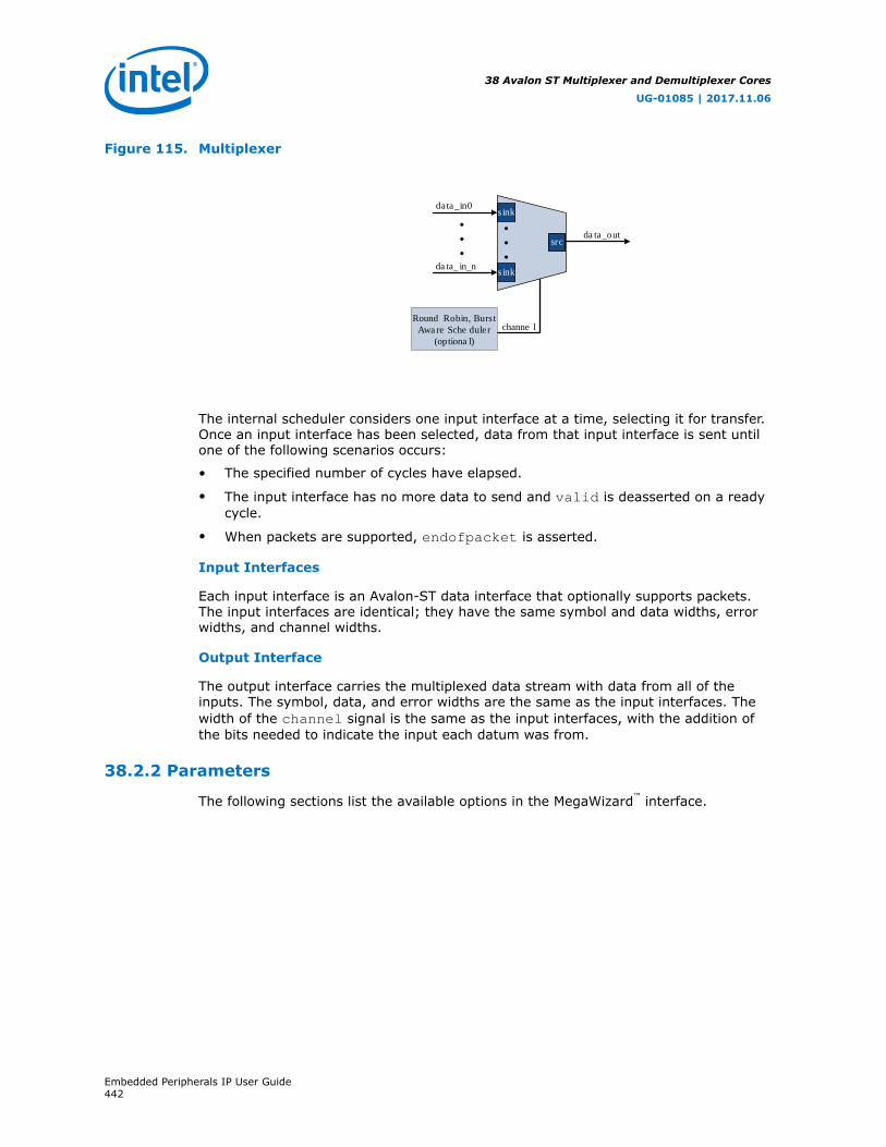
Figure 115. Multiplexer
srcs ink
da ta_ in_n
sink
data_in0
da ta_out
. . .
Round Robin, Burs t Awa re Sche duler
(optiona l)
s ink
s ink
. . .
channe l
The internal scheduler considers one input interface at a time, selecting it for transfer.Once an input interface has been selected, data from that input interface is sent untilone of the following scenarios occurs:
• The specified number of cycles have elapsed.
• The input interface has no more data to send and valid is deasserted on a readycycle.
• When packets are supported, endofpacket is asserted.
Input Interfaces
Each input interface is an Avalon-ST data interface that optionally supports packets.The input interfaces are identical; they have the same symbol and data widths, errorwidths, and channel widths.
Output Interface
The output interface carries the multiplexed data stream with data from all of theinputs. The symbol, data, and error widths are the same as the input interfaces. Thewidth of the channel signal is the same as the input interfaces, with the addition ofthe bits needed to indicate the input each datum was from.
38.2.2 Parameters
The following sections list the available options in the MegaWizard™ interface.
38 Avalon ST Multiplexer and Demultiplexer Cores
UG-01085 | 2017.11.06
Embedded Peripherals IP User Guide442

Functional Parameters
You can configure the following options for the multiplexer:
• Number of Input Ports—The number of input interfaces that the multiplexersupports. Valid values are 2–16.
• Scheduling Size (Cycles)—The number of cycles that are sent from a singlechannel before changing to the next channel.
• Use Packet Scheduling—When this option is on, the multiplexer only switchesthe selected input interface on packet boundaries. Hence, packets on the outputinterface are not interleaved.
• Use high bits to indicate source port—When this option is on, the high bits ofthe output channel signal are used to indicate the input interface that the datacame from. For example, if the input interfaces have 4-bit channel signals, and themultiplexer has 4 input interfaces, the output interface has a 6-bit channel signal.If this parameter is true, bits [5:4] of the output channel signal indicate the inputinterface the data is from, and bits [3:0] are the channel bits that were presentedat the input interface.
Output Interface
You can configure the following options for the output interface:
• Data Bits Per Symbol—The number of bits per symbol for the input and outputinterfaces. Valid values are 1–32 bits.
• Data Symbols Per Beat—The number of symbols (words) that are transferredper beat (transfer). Valid values are 1–32.
• Include Packet Support—Indicates whether or not packet transfers aresupported. Packet support includes the startofpacket, endofpacket, andempty signals.
• Channel Signal Width (bits)—The number of bits used for the channel signalfor input interfaces. A value of 0 indicates that input interfaces do not havechannels. A value of 4 indicates that up to 16 channels share the same inputinterface. The input channel can have a width between 0–31 bits. A value of 0means that the optional channel signal is not used.
• Error Signal Width (bits)—The width of the error signal for input and outputinterfaces. A value of 0 means the error signal is not used.
38.3 Demultiplexer
This section describes the hardware structure and functionality of the demultiplexercomponent.
38.3.1 Functional Description
That Avalon-ST demultiplexer takes data from a channelized input data interface andprovides that data to multiple output interfaces, where the output interface selectedfor a particular transfer is specified by the input channel signal. The data is deliveredto the output interfaces in the same order it was received at the input interface,regardless of the value of channel, packet, frame, or any other signal. Each of theoutput interfaces has the same width as the input interface, so each output interfaceis idle when the demultiplexer is driving data to a different output interface. The
38 Avalon ST Multiplexer and Demultiplexer Cores
UG-01085 | 2017.11.06
Embedded Peripherals IP User Guide443
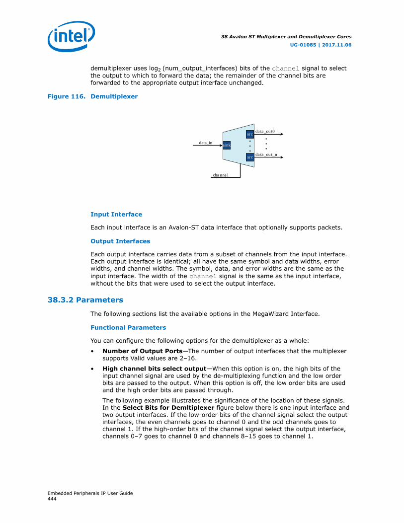
demultiplexer uses log2 (num_output_interfaces) bits of the channel signal to selectthe output to which to forward the data; the remainder of the channel bits areforwarded to the appropriate output interface unchanged.
Figure 116. Demultiplexer
da ta_ou t_n
da ta_ou t0
s inks inkdata_in
src
src
. . . . . .
cha nne l
Input Interface
Each input interface is an Avalon-ST data interface that optionally supports packets.
Output Interfaces
Each output interface carries data from a subset of channels from the input interface.Each output interface is identical; all have the same symbol and data widths, errorwidths, and channel widths. The symbol, data, and error widths are the same as theinput interface. The width of the channel signal is the same as the input interface,without the bits that were used to select the output interface.
38.3.2 Parameters
The following sections list the available options in the MegaWizard Interface.
Functional Parameters
You can configure the following options for the demultiplexer as a whole:
• Number of Output Ports—The number of output interfaces that the multiplexersupports Valid values are 2–16.
• High channel bits select output—When this option is on, the high bits of theinput channel signal are used by the de-multiplexing function and the low orderbits are passed to the output. When this option is off, the low order bits are usedand the high order bits are passed through.
The following example illustrates the significance of the location of these signals.In the Select Bits for Demltiplexer figure below there is one input interface andtwo output interfaces. If the low-order bits of the channel signal select the outputinterfaces, the even channels goes to channel 0 and the odd channels goes tochannel 1. If the high-order bits of the channel signal select the output interface,channels 0–7 goes to channel 0 and channels 8–15 goes to channel 1.
38 Avalon ST Multiplexer and Demultiplexer Cores
UG-01085 | 2017.11.06
Embedded Peripherals IP User Guide444

Figure 117. Select Bits for Demultiplexer
s ink
data_out1
data_out0
s inks ink
da ta_insrc
src
cha nne l<4. .0>
cha nne l<3..0>
cha nne l<3..0>
Input Interface
You can configure the following options for the input interface:
• Data Bits Per Symbol—The number of bits per symbol for the input and outputinterfaces. Valid values are 1 to 32 bits.
• Data Symbols Per Beat—The number of symbols (words) that are transferredper beat (transfer). Valid values are 1 to 32.
• Include Packet Support—Indicates whether or not packet transfers aresupported. Packet support includes the startofpacket, endofpacket, andempty signals.
• Channel Signal Width (bits)—The number of bits used for the channel signalfor output interfaces. A value of 0 means that output interfaces do not use theoptional channel signal.
• Error Signal Width (bits)—The width of the error signal for input and outputinterfaces. A value of 0 means the error signal is not unused.
38.4 Hardware Simulation Considerations
The multiplexer and demultiplexer components do not provide a simulation testbenchfor simulating a stand-alone instance of the component. However, you can use thestandard Platform Designer simulation flow to simulate the component design filesinside an Platform Designer system.
38.5 Software Programming Model
The multiplexer and demultiplexer components do not have any user-visible control orstatus registers. Therefore, software cannot control or configure any aspect of themultiplexer or de-multiplexer at run-time. The components cannot generateinterrupts.
38 Avalon ST Multiplexer and Demultiplexer Cores
UG-01085 | 2017.11.06
Embedded Peripherals IP User Guide445

38.6 Document Revision History
Table 347. Avalon Streaming Channel Multiplexer and Demultiplexer Cores RevisionHistory
Date Version Changes
December 2010 v10.1.0 Removed the “Device Support”, “Instantiating the Core in SOPC Builder”,and “Referenced Documents” sections.
July 2010 v10.0.0 No change from previous release.
November 2009 v9.1.0 No change from previous release.
March 2009 v9.0.0 No change from previous release.
November 2008 v8.1.0 Changed to 8-1/2 x 11 page size. Added parameter Include PacketSupport.
May 2008 v8.0.0 No change from previous release.
38 Avalon ST Multiplexer and Demultiplexer Cores
UG-01085 | 2017.11.06
Embedded Peripherals IP User Guide446

39 Avalon-ST Bytes to Packets and Packets to BytesConverter Cores
39.1 Core Overview
The Avalon Streaming (Avalon-ST) Bytes to Packets and Packets to Bytes Convertercores allow an arbitrary stream of packets to be carried over a byte interface, byencoding packet-related control signals such as startofpacket and endofpacketinto byte sequences.The Avalon-ST Packets to Bytes Converter core encodes packetcontrol and payload as a stream of bytes. The Avalon-ST Bytes to Packets Convertercore accepts an encoded stream of bytes, and converts it into a stream of packets.
The SPI Slave to Avalon Master Bridge and JTAG to Avalon Master Bridge are examplesof how the cores are used.
For more information about the bridge, refer to SPI Slave/JTAG to Avalon MasterBridge Cores
39.2 Functional Description
The following two figures show block diagrams of the Avalon-ST Bytes to Packets andPackets to Bytes Converter cores.
Figure 118. Avalon-ST Bytes to Packets Converter Core
Ava
lon-
ST
S
ink
Avalon-STBytes to Packets
Converter
data_in(bytes)
TS-
nola
vAec
ruoS data_out
(packet)
Figure 119. Avalon-ST Packets to Bytes Converter Core
Ava
lon-
ST
Sour
ce Avalon-STPackets to Bytes
Converter
data_in(packet)
TS-
nola
vASink
data_out(bytes)
UG-01085 | 2017.11.06
Intel Corporation. All rights reserved. Intel, the Intel logo, Altera, Arria, Cyclone, Enpirion, MAX, Nios, Quartusand Stratix words and logos are trademarks of Intel Corporation or its subsidiaries in the U.S. and/or othercountries. Intel warrants performance of its FPGA and semiconductor products to current specifications inaccordance with Intel's standard warranty, but reserves the right to make changes to any products and servicesat any time without notice. Intel assumes no responsibility or liability arising out of the application or use of anyinformation, product, or service described herein except as expressly agreed to in writing by Intel. Intelcustomers are advised to obtain the latest version of device specifications before relying on any publishedinformation and before placing orders for products or services.*Other names and brands may be claimed as the property of others.
ISO9001:2008Registered

39.2.1 Interfaces
Table 348. Properties of Avalon-ST Interfaces
Feature Property
Backpressure Ready latency = 0.
Data Width Data width = 8 bits; Bits per symbol = 8.
Channel Supported, up to 255 channels.
Error Not used.
Packet Supported only on the Avalon-ST Bytes to Packet Converter core’s source interface and the Avalon-ST Packet to Bytes Converter core’s sink interface.
For more information about Avalon-ST interfaces, refer to the Avalon InterfaceSpecifications.
39.2.2 Operation—Avalon-ST Bytes to Packets Converter Core
The Avalon-ST Bytes to Packets Converter core receives streams of bytes andtransforms them into packets. When parsing incoming bytestreams, the core decodesspecial characters in the following manner, with higher priority operations listed first:
• Escape (0x7d)—The core drops the byte. The next byte is XOR'ed with 0x20.
• Start of packet (0x7a)—The core drops the byte and marks the next payload byteas the start of a packet by asserting the startofpacket signal on the Avalon-STsource interface.
• End of packet (0x7b)—The core drops the byte and marks the following byte asthe end of a packet by asserting the endofpacket signal on the Avalon-ST sourceinterface. For single beat packets, both the startofpacket and endofpacketsignals are asserted in the same clock cycle.
There are two possible cases if the payload is a special character:
— The byte sent after end of packet is ESC'ed and XOR'ed with 0x20.
— The byte sent after end of packet is assumed to be the last byte regardless ofwhether or not it is a special character.
Note: The escape character should be used after an end of packet if the nextcharacter requires it.
• Channel number indicator (0x7c)—The core drops the byte and takes the nextnon-special character as the channel number.
Figure 120. Examples of Bytestreams
39 Avalon-ST Bytes to Packets and Packets to Bytes Converter Cores
UG-01085 | 2017.11.06
Embedded Peripherals IP User Guide448
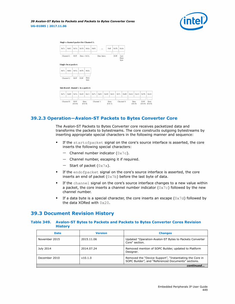
0x7c 0x01 0x7a 0x7d 0x5a 0x01 0xff 0x7b 0x3a...
Channel 1 SO P Data = 0x7a Data byte s EOP Las tDatabyte
Singl e -channel packet fo r Channel 1:
0x7c 0x02 0x7a 0x7b 0x3a
Channel 2 SO P EOP Databyte
Singl e -be at packet:
0x7c 0x00 0x7a 0x10 0x11 0x30 0x31 0x7b 0x14
Channel 0 SO P(Ch 0)
Data (Ch 0)
EOP(Ch 0)
Data(Ch 0)
Interleaved channel s in a pack et:
0x7c 0x01 0x7c 0x00 0x12 0x13
Channel 1 Data (Ch 1)
Cha nnel 0 Data(Ch 0)
39.2.3 Operation—Avalon-ST Packets to Bytes Converter Core
The Avalon-ST Packets to Bytes Converter core receives packetized data andtransforms the packets to bytestreams. The core constructs outgoing bytestreams byinserting appropriate special characters in the following manner and sequence:
• If the startofpacket signal on the core's source interface is asserted, the coreinserts the following special characters:
— Channel number indicator (0x7c).
— Channel number, escaping it if required.
— Start of packet (0x7a).
• If the endofpacket signal on the core's source interface is asserted, the coreinserts an end of packet (0x7b) before the last byte of data.
• If the channel signal on the core’s source interface changes to a new value withina packet, the core inserts a channel number indicator (0x7c) followed by the newchannel number.
• If a data byte is a special character, the core inserts an escape (0x7d) followed bythe data XORed with 0x20.
39.3 Document Revision History
Table 349. Avalon-ST Bytes to Packets and Packets to Bytes Converter Cores RevisionHistory
Date Version Changes
November 2015 2015.11.06 Updated "Operation-Avalon-ST Bytes to Packets ConverterCore" section.
July 2014 2014.07.24 Removed mention of SOPC Builder, updated to PlatformDesigner.
December 2010 v10.1.0 Removed the “Device Support”, “Instantiating the Core inSOPC Builder”, and “Referenced Documents” sections.
continued...
39 Avalon-ST Bytes to Packets and Packets to Bytes Converter Cores
UG-01085 | 2017.11.06
Embedded Peripherals IP User Guide449
Date Version Changes
July 2010 v10.0.0 No change from previous release.
November 2009 v9.1.0 No change from previous release.
March 2009 v9.0.0 No change from previous release.
November 2008 v8.1.0 Changed to 8-1/2 x 11 page size. No change to content.
May 2008 v8.0.0 Initial release.
39 Avalon-ST Bytes to Packets and Packets to Bytes Converter Cores
UG-01085 | 2017.11.06
Embedded Peripherals IP User Guide450

40 Avalon-ST Delay Core
40.1 Core Overview
The Avalon Streaming (Avalon-ST) Delay core provides a solution to delay Avalon-STtransactions by a constant number of clock cycles. This core supports up to 16 clockcycle delays.
The Avalon-ST Delay core is Platform Designer-ready and integrates easily into anyPlatform Designer-generated system.
40.2 Functional Description
Figure 121. Avalon-ST Delay Core
Avalon-STDelay Core
Aval
on-S
T Si
nk
Avalon-ST SourceClock
Out_DataIn_Data
The Avalon-ST Delay core adds a delay between the input and output interfaces. Thecore accepts all transactions presented on the input interface and reproduces them onthe output interface N cycles later without changing the transaction.
The input interface delays the input signals by a constant (N) number of clock cyclesto the corresponding output signals of the Avalon-ST output interface. The NumberOf Delay Clocks parameter defines the constant (N) number, which must be between0 and 16. The change of the In_Valid signal is reflected on the Out_Valid signalexactly N cycles later.
40.2.1 Reset
The Avalon-ST Delay core has a reset signal that is synchronous to the clk signal.When the core asserts the reset signal, the output signals are held at 0. After thereset signal is deasserted, the output signals are held at 0 for N clock cycles. Thedelayed values of the input signals are then reflected at the output signals after Nclock cycles.
UG-01085 | 2017.11.06
Intel Corporation. All rights reserved. Intel, the Intel logo, Altera, Arria, Cyclone, Enpirion, MAX, Nios, Quartusand Stratix words and logos are trademarks of Intel Corporation or its subsidiaries in the U.S. and/or othercountries. Intel warrants performance of its FPGA and semiconductor products to current specifications inaccordance with Intel's standard warranty, but reserves the right to make changes to any products and servicesat any time without notice. Intel assumes no responsibility or liability arising out of the application or use of anyinformation, product, or service described herein except as expressly agreed to in writing by Intel. Intelcustomers are advised to obtain the latest version of device specifications before relying on any publishedinformation and before placing orders for products or services.*Other names and brands may be claimed as the property of others.
ISO9001:2008Registered

40.2.2 Interfaces
The Avalon-ST Delay core supports packetized and non-packetized interfaces withoptional channel and error signals. This core does not support backpressure.
Table 350. Properties of Avalon-ST Interfaces
Feature Property
Backpressure Not supported.
Data Width Configurable.
Channel Supported (optional).
Error Supported (optional).
Packet Supported (optional).
For more information about Avalon-ST interfaces, refer to the Avalon InterfaceSpecifications.
40.3 Parameters
Table 351. Configurable Parameters
Parameter Legal Values DefaultValue
Description
Number Of Delay Clocks 0 to 16 1 Specifies the delay the core introduces, in clock cycles.The value of 0 is supported for some cases ofparameterized systems in which no delay is required.
Data Width 1–512 8 The width of the data on the Avalon-ST data interfaces.
Bits Per Symbol 1–512 8 The number of bits per symbol for the input and outputinterfaces. For example, byte-oriented interfaces have 8-bit symbols.
Use Packets 0 or 1 0 Indicates whether or not packet transfers are supported.Packet support includes the startofpacket,endofpacket, and empty signals.
Use Channel 0 or 1 0 The option to enable or disable the channel signal.
Channel Width 0-8 1 The width of the channel signal on the data interfaces.This parameter is disabled when Use Channel is set to 0.
Max Channels 0-255 1 The maximum number of channels that a data interfacecan support. This parameter is disabled when UseChannel is set to 0.
Use Error 0 or 1 0 The option to enable or disable the error signal.
Error Width 0–31 1 The width of the error signal on the output interfaces. Avalue of 0 indicates that the error signal is not in use. Thisparameter is disabled when Use Error is set to 0.
Use packets 0 or 1 Setting this parameter to 1 enables packet support on theAvalon-ST data interfaces.
Use fill level 0 or 1 Setting this parameter to 1 enables the Avalon-MM statusinterface.
continued...
40 Avalon-ST Delay Core
UG-01085 | 2017.11.06
Embedded Peripherals IP User Guide452
Parameter Legal Values DefaultValue
Description
Number of almost-full thresholds 0 to 2 The number of almost-full thresholds to enable. Settingthis parameter to 1 enables Use almost-full threshold1. Setting it to 2 enables both Use almost-full threshold1 and Use almost-full threshold 2.
Number of almost-emptythresholds
0 to 2 The number of almost-empty thresholds to enable. Settingthis parameter to 1 enables Use almost-emptythreshold 1. Setting it to 2 enables both Use almost-empty threshold 1 and Use almost-empty threshold2.
Section available threshold 0 to 2AddressWidth
Specify the amount of data to be delivered to the outputinterface. This parameter applies only when packetsupport is disabled.
Packet buffer mode 0 or 1 Setting this parameter to 1 causes the core to deliver onlyfull packets to the output interface. This parameter appliesonly when Use packets is set to 1.
Drop on error 0 or 1 Setting this parameter to 1 causes the core to droppackets at the Avalon-ST data sink interface if the errorsignal on that interface is asserted. Otherwise, the coreaccepts the packet and sends it out on the Avalon-ST datasource interface with the same error. This parameterapplies only when packet buffer mode is enabled.
Use almost-full threshold 1 0 or 1 This threshold indicates that the FIFO is almost full. It isenabled when the parameter Number of almost-fullthreshold is set to 1 or 2.
Use almost-full threshold 2 0 or 1 This threshold is an initial indication that the FIFO isgetting full. It is enabled when the parameter Number ofalmost-full threshold is set to 2.
Use almost-empty threshold 1 0 or 1 This threshold indicates that the FIFO is almost empty. Itis enabled when the parameter Number of almost-empty threshold is set to 1 or 2.
Use almost-empty threshold 2 0 or 1 This threshold is an initial indication that the FIFO isgetting empty. It is enabled when the parameter Numberof almost-empty threshold is set to 2.
40.4 Document Revision History
Table 352. Avalon-ST Delay Core Revision History
Date Version Changes
December 2010 v10.1.0 Removed the “Device Support”, “Instantiating the Core in SOPC Builder”,and “Referenced Documents” sections.
July 2010 v10.0.0 No change from previous release.
January 2010 v9.1.1 Initial release.
40 Avalon-ST Delay Core
UG-01085 | 2017.11.06
Embedded Peripherals IP User Guide453
41 Avalon-ST Round Robin Scheduler Core
41.1 Core Overview
Avalon Streaming (Avalon-ST) components in Platform Designer provide a channelinterface to stream data from multiple channels into a single component. In a multi-channel Avalon-ST component that stores data, the component can store data eitherin the sequence that it comes in (FIFO) or in segments according to the channel.When data is stored in segments according to channels, a scheduler is needed toschedule the read operations from that particular component. The most basic of theschedulers is the Avalon-ST Round Robin Scheduler core.
The Avalon-ST Round Robin Scheduler core is Platform Designer-ready and canintegrate easily into any Platform Designer-generated systems.
41.2 Performance and Resource Utilization
This section lists the resource utilization and performance data for various Intel FPGAdevice families. The estimates are obtained by compiling the core using the IntelQuartus Prime software.
The table below shows the resource utilization and performance data for a Stratix IIGX device (EP2SGX130GF1508I4).
Table 353. Resource Utilization and Performance Data for Stratix II GX Devices
Number of Channels ALUTs Logic Registers Memory M512/M4K/M-RAM
fMAX(MHz)
4 7 7 0/0/0 > 125
12 25 17 0/0/0 > 125
24 62 30 0/0/0 > 125
The table below shows the resource utilization and performance data for a Stratix IIIdevice (EP3SL340F1760C3). The performance of the IP Core in Stratix IV devices issimilar to Stratix III devices.
Table 354. Resource Utilization and Performance Data for Stratix III Devices
Number of Channels ALUTs Logic Registers Memory M9K/M144K/ MLAB
fMAX(MHz)
4 7 7 0/0/0 > 125
12 25 17 0/0/0 > 125
24 67 30 0/0/0 > 125
UG-01085 | 2017.11.06
Intel Corporation. All rights reserved. Intel, the Intel logo, Altera, Arria, Cyclone, Enpirion, MAX, Nios, Quartusand Stratix words and logos are trademarks of Intel Corporation or its subsidiaries in the U.S. and/or othercountries. Intel warrants performance of its FPGA and semiconductor products to current specifications inaccordance with Intel's standard warranty, but reserves the right to make changes to any products and servicesat any time without notice. Intel assumes no responsibility or liability arising out of the application or use of anyinformation, product, or service described herein except as expressly agreed to in writing by Intel. Intelcustomers are advised to obtain the latest version of device specifications before relying on any publishedinformation and before placing orders for products or services.*Other names and brands may be claimed as the property of others.
ISO9001:2008Registered
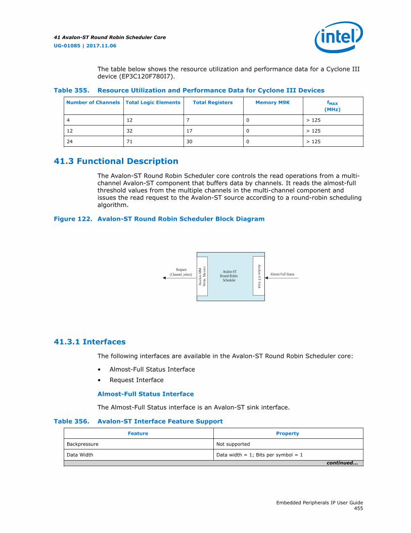
The table below shows the resource utilization and performance data for a Cyclone IIIdevice (EP3C120F780I7).
Table 355. Resource Utilization and Performance Data for Cyclone III Devices
Number of Channels Total Logic Elements Total Registers Memory M9K fMAX(MHz)
4 12 7 0 > 125
12 32 17 0 > 125
24 71 30 0 > 125
41.3 Functional Description
The Avalon-ST Round Robin Scheduler core controls the read operations from a multi-channel Avalon-ST component that buffers data by channels. It reads the almost-fullthreshold values from the multiple channels in the multi-channel component andissues the read request to the Avalon-ST source according to a round-robin schedulingalgorithm.
Figure 122. Avalon-ST Round Robin Scheduler Block Diagram
Request(Channel_select) Almost Full Status
Avalon-STRound-Robin
Scheduler
M
M-nolavA
retsaM etir
W
kni
S T
S-n o
lav
A
41.3.1 Interfaces
The following interfaces are available in the Avalon-ST Round Robin Scheduler core:
• Almost-Full Status Interface
• Request Interface
Almost-Full Status Interface
The Almost-Full Status interface is an Avalon-ST sink interface.
Table 356. Avalon-ST Interface Feature Support
Feature Property
Backpressure Not supported
Data Width Data width = 1; Bits per symbol = 1
continued...
41 Avalon-ST Round Robin Scheduler Core
UG-01085 | 2017.11.06
Embedded Peripherals IP User Guide455
Feature Property
Channel Maximum channel = 32; Channel width = 5
Error Not supported
Packet Not supported
The interface collects the almost-full status from the sink components for all thechannels in the sequence provided.
Request Interface
The Request Interface is an Avalon Memory-Mapped (MM) Write Master interface. Thisinterface requests data from a specific channel. The Avalon-ST Round Robin Schedulercore cycles through all of the channels it supports and schedules data to be read.
41.3.2 Operations
If a particular channel is almost full, the Avalon-ST Round Robin Scheduler will notschedule data to be read from that channel in the source component.
The Avalon-ST Round Robin Scheduler only requests 1 beat of data from a channel ateach transaction. To request 1 beat of data from channel n, the scheduler writes thevalue 1 to address (4 ×n). For example, if the scheduler is requesting data fromchannel 3, the scheduler writes 1 to address 0xC.
At every clock cycle, the Avalon-ST Round Robin Scheduler requests data from thenext channel. Therefore, if the Avalon-ST Round Robin Scheduler starts requestingfrom channel 1, at the next clock cycle, it requests from channel 2. The Avalon-STRound Robin Scheduler does not request data from a particular channel if the almost-full status for the channel is asserted. In this case, one clock cycle is used without arequest transaction.
The Avalon-ST Round Robin Scheduler cannot determine if the requested componentis able to service the request transaction. The component asserts waitrequest whenit cannot accept new requests.
Table 357. Ports for the Avalon-ST Round Robin Scheduler
Signal Direction Description
Clock and Reset
clk In Clock reference.
reset_n In Asynchronous active low reset.
Avalon-MM Request Interface
request_address (log2Max_Channels–1:0)
Out The write address used to signal the channel the request isfor.
request_write Out Write enable signal.
request_writedata Out The amount of data requested from the particular channel.This value is always fixed at 1.
request_waitrequest In Wait request signal, used to pause the scheduler when theslave cannot accept a new request.
continued...
41 Avalon-ST Round Robin Scheduler Core
UG-01085 | 2017.11.06
Embedded Peripherals IP User Guide456
Signal Direction Description
Avalon-ST Almost-Full Status Interface
almost_full_valid In Indicates that almost_full_channel andalmost_full_data are valid.
almost_full_channel(Channel_Width–1:0)
In Indicates the channel for the current status indication.
almost_full_data (log2Max_Channels–1:0)
In A 1-bit signal that is asserted high to indicate that thechannel indicated by almost_full_channel is almostfull.
41.4 Parameters
Table 358. Parameters for Avalon-ST Round Robin Scheduler Component
Parameters Values Description
Number of channels 2–32 Specifies the number of channels the Avalon-ST Round Robin Schedulersupports.
Use almost-full status 0–1 Specifies whether the almost-full interface is used. If the interface is not used,the core always requests data from the next channel at the next clock cycle.
41.5 Document Revision History
Table 359. Avalon-ST Round Robin Scheduler Core Revision History
Date Version Changes
December 2010 v10.1.0 Removed the “Device Support”, “Instantiating the Core in SOPC Builder”,and “Referenced Documents” sections.
July 2010 v10.0.0 No change from previous release.
November 2009 v9.1.0 No change from previous release.
March 2009 v9.0.0 No change from previous release.
November 2008 v8.1.0 Changed to 8-1/2 x 11 page size. No change to content.
May 2008 v8.0.0 Initial release.
41 Avalon-ST Round Robin Scheduler Core
UG-01085 | 2017.11.06
Embedded Peripherals IP User Guide457
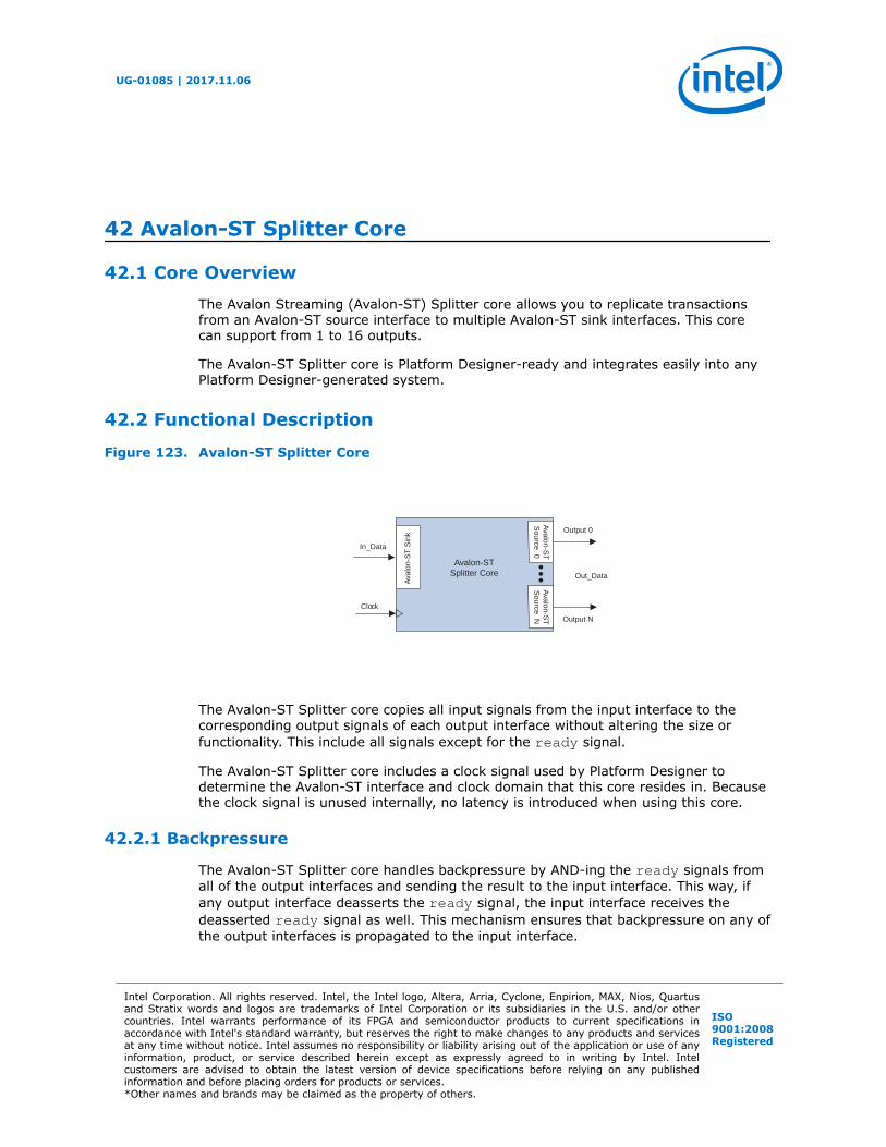
42 Avalon-ST Splitter Core
42.1 Core Overview
The Avalon Streaming (Avalon-ST) Splitter core allows you to replicate transactionsfrom an Avalon-ST source interface to multiple Avalon-ST sink interfaces. This corecan support from 1 to 16 outputs.
The Avalon-ST Splitter core is Platform Designer-ready and integrates easily into anyPlatform Designer-generated system.
42.2 Functional Description
Figure 123. Avalon-ST Splitter Core
Output 0
In_Data
Out_Data
Avalon-STSplitter Core
Output N
Clock
Av
kniS
TS-nola
Av
TS -
n ol a
oS
urce 0A
vT
S -no
l ao
Surce N
The Avalon-ST Splitter core copies all input signals from the input interface to thecorresponding output signals of each output interface without altering the size orfunctionality. This include all signals except for the ready signal.
The Avalon-ST Splitter core includes a clock signal used by Platform Designer todetermine the Avalon-ST interface and clock domain that this core resides in. Becausethe clock signal is unused internally, no latency is introduced when using this core.
42.2.1 Backpressure
The Avalon-ST Splitter core handles backpressure by AND-ing the ready signals fromall of the output interfaces and sending the result to the input interface. This way, ifany output interface deasserts the ready signal, the input interface receives thedeasserted ready signal as well. This mechanism ensures that backpressure on any ofthe output interfaces is propagated to the input interface.
UG-01085 | 2017.11.06
Intel Corporation. All rights reserved. Intel, the Intel logo, Altera, Arria, Cyclone, Enpirion, MAX, Nios, Quartusand Stratix words and logos are trademarks of Intel Corporation or its subsidiaries in the U.S. and/or othercountries. Intel warrants performance of its FPGA and semiconductor products to current specifications inaccordance with Intel's standard warranty, but reserves the right to make changes to any products and servicesat any time without notice. Intel assumes no responsibility or liability arising out of the application or use of anyinformation, product, or service described herein except as expressly agreed to in writing by Intel. Intelcustomers are advised to obtain the latest version of device specifications before relying on any publishedinformation and before placing orders for products or services.*Other names and brands may be claimed as the property of others.
ISO9001:2008Registered

When the Qualify Valid Out parameter is set to 1, the Out_Valid signals on allother output interfaces are gated when backpressure is applied from one outputinterface. In this case, when any output interface deasserts its ready signal, theOut_Valid signals on the rest of the output interfaces are deasserted as well.
When the Qualify Valid Out parameter is set to 0, the output interfaces have a non-gated Out_Valid signal when backpressure is applied. In this case, when an outputinterface deasserts its ready signal, the Out_Valid signals on the rest of the outputinterfaces are not affected.
Because the logic is purely combinational, the core introduces no latency.
42.2.2 Interfaces
The Avalon-ST Splitter core supports packetized and non-packetized interfaces withoptional channel and error signals. The core propagates backpressure from any outputinterface to the input interface.
Table 360. Properties of Avalon-ST Interfaces
Feature Property
Backpressure Ready latency = 0.
Data Width Configurable.
Channel Supported (optional).
Error Supported (optional).
Packet Supported (optional).
For more information about Avalon-ST interfaces, refer to the Avalon InterfaceSpecifications.
42.3 Parameters
Table 361. Configurable Parameters
Parameter Legal Values DefaultValue
Description
Number Of Outputs 1 to 16 2 The number of output interfaces. The value of 1 is supported forsome cases of parameterized systems in which no duplicatedoutput is required.
Qualify Valid Out 0 or 1 1 Determines whether the Out_Valid signal is gated or non-gatedwhen backpressure is applied.
Data Width 1–512 8 The width of the data on the Avalon-ST data interfaces.
Bits Per Symbol 1–512 8 The number of bits per symbol for the input and outputinterfaces. For example, byte-oriented interfaces have 8-bitsymbols.
Use Packets 0 or 1 0 Indicates whether or not packet transfers are supported. Packetsupport includes the startofpacket, endofpacket, andempty signals.
Use Channel 0 or 1 0 The option to enable or disable the channel signal.
continued...
42 Avalon-ST Splitter Core
UG-01085 | 2017.11.06
Embedded Peripherals IP User Guide459
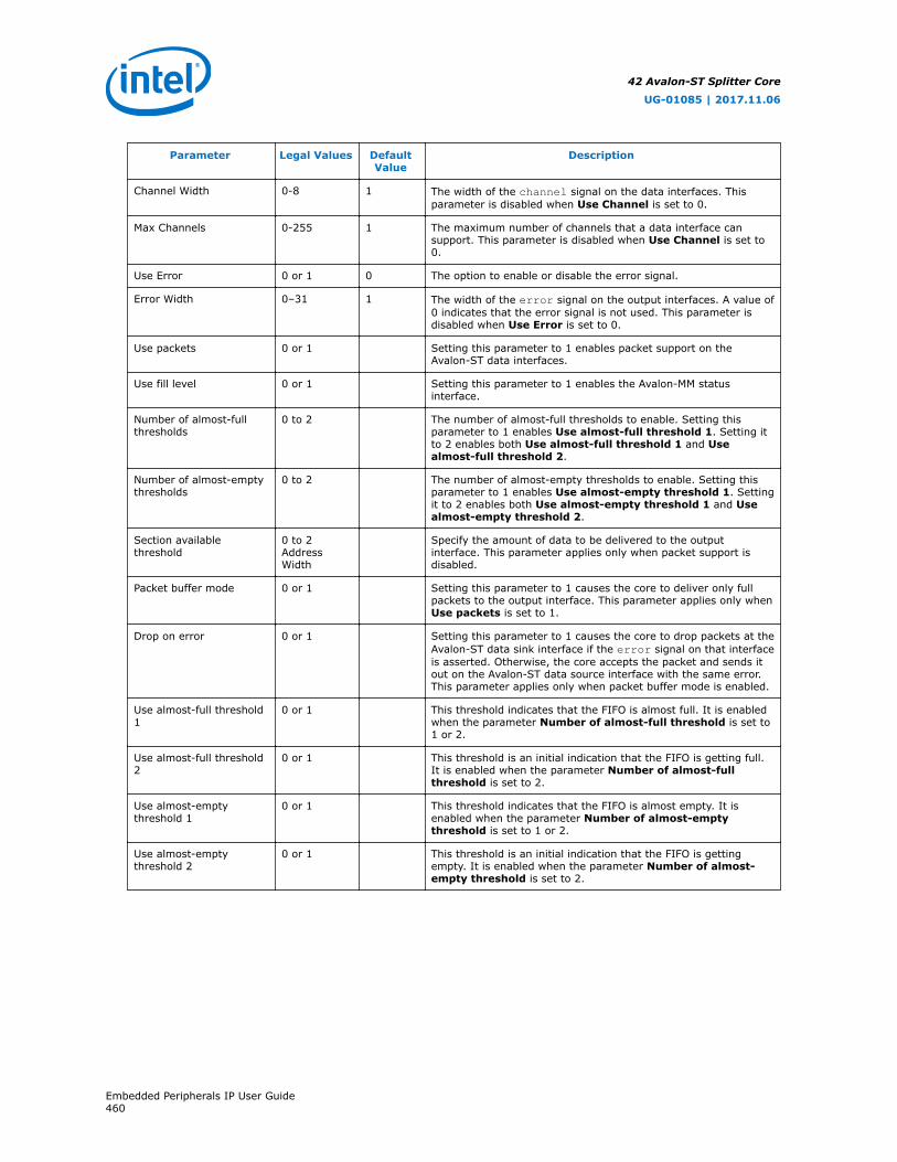
Parameter Legal Values DefaultValue
Description
Channel Width 0-8 1 The width of the channel signal on the data interfaces. Thisparameter is disabled when Use Channel is set to 0.
Max Channels 0-255 1 The maximum number of channels that a data interface cansupport. This parameter is disabled when Use Channel is set to0.
Use Error 0 or 1 0 The option to enable or disable the error signal.
Error Width 0–31 1 The width of the error signal on the output interfaces. A value of0 indicates that the error signal is not used. This parameter isdisabled when Use Error is set to 0.
Use packets 0 or 1 Setting this parameter to 1 enables packet support on theAvalon-ST data interfaces.
Use fill level 0 or 1 Setting this parameter to 1 enables the Avalon-MM statusinterface.
Number of almost-fullthresholds
0 to 2 The number of almost-full thresholds to enable. Setting thisparameter to 1 enables Use almost-full threshold 1. Setting itto 2 enables both Use almost-full threshold 1 and Usealmost-full threshold 2.
Number of almost-emptythresholds
0 to 2 The number of almost-empty thresholds to enable. Setting thisparameter to 1 enables Use almost-empty threshold 1. Settingit to 2 enables both Use almost-empty threshold 1 and Usealmost-empty threshold 2.
Section availablethreshold
0 to 2AddressWidth
Specify the amount of data to be delivered to the outputinterface. This parameter applies only when packet support isdisabled.
Packet buffer mode 0 or 1 Setting this parameter to 1 causes the core to deliver only fullpackets to the output interface. This parameter applies only whenUse packets is set to 1.
Drop on error 0 or 1 Setting this parameter to 1 causes the core to drop packets at theAvalon-ST data sink interface if the error signal on that interfaceis asserted. Otherwise, the core accepts the packet and sends itout on the Avalon-ST data source interface with the same error.This parameter applies only when packet buffer mode is enabled.
Use almost-full threshold1
0 or 1 This threshold indicates that the FIFO is almost full. It is enabledwhen the parameter Number of almost-full threshold is set to1 or 2.
Use almost-full threshold2
0 or 1 This threshold is an initial indication that the FIFO is getting full.It is enabled when the parameter Number of almost-fullthreshold is set to 2.
Use almost-emptythreshold 1
0 or 1 This threshold indicates that the FIFO is almost empty. It isenabled when the parameter Number of almost-emptythreshold is set to 1 or 2.
Use almost-emptythreshold 2
0 or 1 This threshold is an initial indication that the FIFO is gettingempty. It is enabled when the parameter Number of almost-empty threshold is set to 2.
42 Avalon-ST Splitter Core
UG-01085 | 2017.11.06
Embedded Peripherals IP User Guide460

42.4 Document Revision History
Table 362. Avalon-ST Splitter Core Revision History
Date Version Changes
December 2010 v10.1.0 Removed the “Device Support”, “Instantiating the Core in SOPC Builder”,and “Referenced Documents” sections.
July 2010 v10.0.0 No change from previous release.
January 2010 v9.1.1 Initial release.
42 Avalon-ST Splitter Core
UG-01085 | 2017.11.06
Embedded Peripherals IP User Guide461

43 Avalon-MM DDR Memory Half Rate Bridge Core
43.1 Core Overview
The Avalon Memory-Mapped (MM) Half-Rate Bridge core is a special-purpose clock-crossing bridge intended for CPUs that require low-latency access to high-speedmemory. The core works under the assumption that the memory clock is twice thefrequency of the CPU clock, with zero phase shift between the two. It allows highspeed memory to run at full rate while providing low-latency interface for a CPU toaccess it by using lightweight logic that translates one single-word request into a two-word burst to a memory running at twice the clock frequency and half the width. Forsystems with a 8-bit DDR interface, using the Half-Rate DDR Bridge in conjunctionwith a DDR SDRAM high-performance memory controller creates a datapath thatmatches the throughput of the DDR memory to the CPU. This half-rate bridge providesthe same functionality as the clock crossing bridge, but with significantly lower latency—2 cycles instead of 12.
The core’s master interface is designed to be connected to a high-speed DDR SDRAMcontroller and thus only supports bursting. Because the slave interface is designed toreceive single-word requests, it does not support bursting. The figure below shows asystem including an 8-bit DDR memory, a high-performance memory controller, theHalf-Rate DDR Bridge, and a CPU.
Figure 124. Platform Designer Memory System Using a DDR Memory Half-Rate Bridge
8
DDR Clk <-----------> Controller Clk <-----------> Controller Clk/2
16DDR2/3 HighPerformance
Controller(full rate)
FPGA
PCB
32DDRn
burst count = 4 burst count = 2 burst count = 1
Half-RateBridge
SS M M CPU
The Avalon-MM DDR Memory Half-Rate Bridge core has the following features andrequirements:
• Platform Designer ready with Timing Analyzer Timing Analyzer constraints
• Requires master clock and slave clock to be synchronous
• Handles different bus sizes between CPU and memory
• Requires the frequency of the master clock to be double of the slave clock
• Has configurable address and data port widths in the master interface
UG-01085 | 2017.11.06
Intel Corporation. All rights reserved. Intel, the Intel logo, Altera, Arria, Cyclone, Enpirion, MAX, Nios, Quartusand Stratix words and logos are trademarks of Intel Corporation or its subsidiaries in the U.S. and/or othercountries. Intel warrants performance of its FPGA and semiconductor products to current specifications inaccordance with Intel's standard warranty, but reserves the right to make changes to any products and servicesat any time without notice. Intel assumes no responsibility or liability arising out of the application or use of anyinformation, product, or service described herein except as expressly agreed to in writing by Intel. Intelcustomers are advised to obtain the latest version of device specifications before relying on any publishedinformation and before placing orders for products or services.*Other names and brands may be claimed as the property of others.
ISO9001:2008Registered

43.2 Resource Usage and Performance
This section lists the resource usage and performance data for supported deviceswhen operating the Half-Rate Bridge with a full-rate DDR SDRAM high-performancememory controller.
Using the Half-Rate Bridge with a full-rate DDR SDRAM high-performance memorycontroller results an average of 48% performance improvement over a system using ahalf-rate DDR SDRAM high-performance memory controller in a series of embeddedapplications. The performance improvement is 62.2% based on the Dhrystonebenchmark, and 87.7% when accessing memory bypassing the cache. For memorysystems that use the Half-Rate bridge in conjunction with DDR2/3 High PerformanceController, the data throughput is the same on the Half-Rate Bridge master and slaveinterfaces. The decrease in memory latency on the Half-Rate Bridge slave interfaceresults in higher performance for the processor.
The table below shows the resource usage for Stratix II and Stratix III devices in theIntel Quartus Prime software with a data width of 16 bits, an address span of 24 bits.
Table 363. Resource Utilization Data for Stratix II and Stratix III Devices
Device Family Combinational ALUTs ALMs Logic Register Embedded Memory
Stratix II 61 134 153 0
Stratix III 60 138 153 0
Table 364. Resource Utilization Data for Cyclone III Devices
Logic Cells (LC) Logic Register LUT-only LC Register-only LC LUT/Register LCs EmbeddedMemory
233 152 33 84 121 0
43.3 Functional Description
The Avalon MM DDR Memory Half Rate Bridge works under two constraints:
• Its memory-side master has a clock frequency that is synchronous (zero phaseshift) to, and twice the frequency of, the CPU-side slave.
• Its memory-side master is half as wide as its CPU-side slave.
The bridge leverages these two constraints to provide lightweight, low-latency clock-crossing logic between the CPU and the memory. These constraints are in contrastwith the Avalon-MM Clock-Crossing Bridge, which makes no assumptions about thefrequency/phase relationship between the master- and slave-side clocks, and provideshigher-latency logic that fully-synchronizes all signals that pass between the twodomains.
The Avalon MM DDR Memory Half-Rate Bridge has an Avalon-MM slave interface thataccepts single-word (non-bursting) transactions. When the slave interface receives atransaction from a connected CPU, it issues a two-word burst transaction on its masterinterface (which is half as wide and twice as fast). If the transaction is a read request,the bridge's master interface waits for the slave’s two-word response, concatenatesthe two words, and presents them as a single readdata word on its slave interface tothe CPU. Every time the data width is halved, the clock rate is doubled. As a result,the data throughput is matched between the CPU and the off-chip memory device.
43 Avalon-MM DDR Memory Half Rate Bridge Core
UG-01085 | 2017.11.06
Embedded Peripherals IP User Guide463

The figure below shows the latency in the Avalon-MM Half-Rate Bridge core. The coreadds two cycles of latency in the slave clock domain for read transactions. The firstcycle is introduced during the command phase of the transaction and the secondcycle, during the response phase of the transaction. The total latency is 2+<x>,where <x> refers to the latency of the DDR SDRAM high-performance memorycontroller. Using the clock crossing bridge for this same purpose would imposeapproximately 12 cycles of additional latency.
Figure 125. Avalon-MM DDR Memory Half-Rate Bridge Block Diagram
DDR2/3 HighPerformance
Controller(full rate)
Half-Rate Bridge
Cmd +1
Rsp +1
Q D
D Q
S SMDDR2/3 Memory CPU
43.4 Instantiating the Core in Platform Designer
Use the IP Catalog in Platform Designer to find the Avalon-MM DDR Memory Half-RateBridge core. In the parameter editor window you can specify the core’s configuration.The table below describes the parameters that can be configured for the Avalon-MMHalf-Rate Bridge core.
Table 365. Configurable Parameters for Avalon-MM DDR Memory Half-Rate Bridge Core
Parameters Allowed Values Default Value Description
Data Width 8, 16, 32, 64, 128, 256, 512 16 The width of the data signalin the master interface.
Address Width 1-32 24 The width of the addresssignal in the masterinterface.
The table below describes the parameters that are derived based on the Data Widthand Address Width settings for the Avalon-MM DDR Memory Half-Rate Bridge core.
Table 366. Derived Parameters for Avalon-MM DDR Memory Half-Rate Bridge Core
Parameter Default Value Description
Master interface’s Byte Enable Width 2 The width of the byte-enable signal inthe master interface.
Slave interface’s Data Width 32 The width of the data signal in theslave interface.
Slave interface’s Address Width 22 The width of the address signal in theslave interface.
Slave interface’s Byte Enable Width 4 The width of the byte-enable signal inthe slave interface.
43 Avalon-MM DDR Memory Half Rate Bridge Core
UG-01085 | 2017.11.06
Embedded Peripherals IP User Guide464
43.5 Example System
The following example provides high-level steps showing how the Avalon-MM DDRMemory Half-Rate Bridge core is connected in a system. This example assumes thatyou are familiar with the Platform Designer GUI.
1. Add a Nios II Processor to the system.
2. Add a DDR2 SDRAM High-Performance Controller and configure it to full-ratemode.
3. Add Avalon-MM DDR Memory Half-Rate Bridge to the system.
4. Configure the parameters of the Avalon-MM DDR Memory Half-Rate Bridge basedon the memory controller. For example, for a 32 MByte DDR memory controller infull rate mode with 8 DQ pins (see Figure 124 on page 462), the parametersshould be set as the following:
• Data Width = 16
For a memory controller that has 8 DQ pins, its local interface width is 16 bits.The local interface width and the data width must be the same, therefore datawidth is set to 16 bits.
• Address Width = 25
For a memory capacity of 32 MBytes, the byte address is 25 bits. Because themaster address of the bridge is byte aligned, the address width is set to 25 bits.
5. Connect altmemddr_auxhalf to the slave clock interface (clk_s1) of the Half-Rate Bridge.
6. Connect altmemddr_sysclk to the master clock interface (clk_m1) of the Half-Rate Bridge.
7. Remove all connections between Nios II processor and the memory controller, ifthere are any.
8. Connect the master interface (m1) of the Avalon-MM DDR Memory Half-RateBridge to the memory controller slave interface.
9. Connect the slave interface (s1) of the Avalon-MM DDR Memory Half-Rate Bridgeto the Nios II processor data_master interface.
10. Connect altmemddr_auxhalf to Nios II processor clock interface.
43.6 Document Revision History
Table 367. Avalon-MM DDR Memory Half Rate Bridge Core Revision History
Date Version Changes
June 2016 2016.06.17 Initial release
43 Avalon-MM DDR Memory Half Rate Bridge Core
UG-01085 | 2017.11.06
Embedded Peripherals IP User Guide465
44 Intel FPGA GMII to RGMII Converter Core
44.1 Core Overview
The Intel FPGA GMII to RGMII converter core is an available soft IP for the FPGAfabric. It converts the GMII/MII interface of the Ethernet controller in the hardprocessor system (HPS) to an RGMII interface. By default, the HPS Ethernet controllercan either provide an RGMII interface on the HPS pins or an GMII/MII interface byusing the FPGA loaner I/O. However, the GMII to RGMII converter offers a solution fordesigners who want to interface to an external RGMII PHY through the FPGA withoutadding external interface logic.
44.2 Feature Description
44.2.1 Supported Features
The following is the list of features supported by the core.
• Perform GMII/MII interface to RGMII interface conversion
• Supports tri-speed (10/100/1000 Mbps) operation
• Supports dynamic speed switching
• Supports generation time option to enable pipeline registers for the transmit andreceive paths
44.2.2 Unsupported Features
The Intel FPGA GMII to RGMII converter core does not support an internal delay of theTX/RX clock. However, the FPGA may still provide the 2 ns delay for center-aligneddata transmission/reception through the FPGA I/O buffer. This delay feature iscommonly supported by the PHY device or handled at the board level.
For more information on Intel Quartus Prime delay settings, refer to your device'sGolden Hardware Reference Design (GHRD) user manual on RocketBoards.org.
Related Links
GSRD User Manual
UG-01085 | 2017.11.06
Intel Corporation. All rights reserved. Intel, the Intel logo, Altera, Arria, Cyclone, Enpirion, MAX, Nios, Quartusand Stratix words and logos are trademarks of Intel Corporation or its subsidiaries in the U.S. and/or othercountries. Intel warrants performance of its FPGA and semiconductor products to current specifications inaccordance with Intel's standard warranty, but reserves the right to make changes to any products and servicesat any time without notice. Intel assumes no responsibility or liability arising out of the application or use of anyinformation, product, or service described herein except as expressly agreed to in writing by Intel. Intelcustomers are advised to obtain the latest version of device specifications before relying on any publishedinformation and before placing orders for products or services.*Other names and brands may be claimed as the property of others.
ISO9001:2008Registered
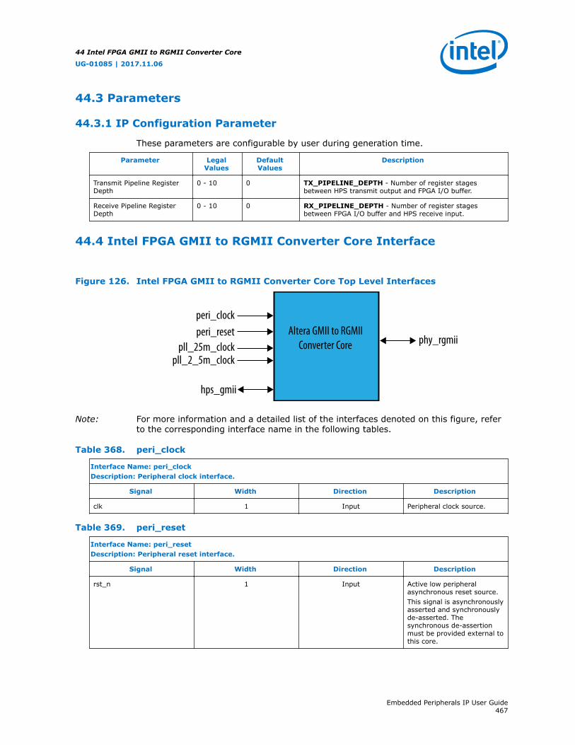
44.3 Parameters
44.3.1 IP Configuration Parameter
These parameters are configurable by user during generation time.
Parameter LegalValues
DefaultValues
Description
Transmit Pipeline RegisterDepth
0 - 10 0 TX_PIPELINE_DEPTH - Number of register stagesbetween HPS transmit output and FPGA I/O buffer.
Receive Pipeline RegisterDepth
0 - 10 0 RX_PIPELINE_DEPTH - Number of register stagesbetween FPGA I/O buffer and HPS receive input.
44.4 Intel FPGA GMII to RGMII Converter Core Interface
Figure 126. Intel FPGA GMII to RGMII Converter Core Top Level Interfaces
Altera GMII to RGMII Converter Core
peri_clockperi_reset
pll_25m_clockpll_2_5m_clock
hps_gmii
phy_rgmii
Note: For more information and a detailed list of the interfaces denoted on this figure, referto the corresponding interface name in the following tables.
Table 368. peri_clock
Interface Name: peri_clockDescription: Peripheral clock interface.
Signal Width Direction Description
clk 1 Input Peripheral clock source.
Table 369. peri_reset
Interface Name: peri_resetDescription: Peripheral reset interface.
Signal Width Direction Description
rst_n 1 Input Active low peripheralasynchronous reset source.This signal is asynchronouslyasserted and synchronouslyde-asserted. Thesynchronous de-assertionmust be provided external tothis core.
44 Intel FPGA GMII to RGMII Converter Core
UG-01085 | 2017.11.06
Embedded Peripherals IP User Guide467
Table 370. pll_25m_clock
Interface Name: pll_25m_clockDescription: 25MHz clock from FPGA PLL output.
Signal Width Direction Description
pll_25m_clk 1 Input 25MHz input clock fromFPGA PLL.
Table 371. pll_2_5m_clock
Interface Name: pll_2_5m_clockDescription: 2.5MHz clock from FPGA PLL output.
Signal Width Direction Description
pll_2_5m_clk 1 Input 2.5MHz input clock fromFPGA PLL.
Table 372. hps_gmii
Interface Name: hps_gmiiDescription: GMII/MII interface facing Intel FPGA HPS Emac Interface Splitter Core
Signal Width Direction Description
mac_tx_clk_o 1 Input GMII/MII transmit clockfrom HPS
mac_tx_clk_i 1 Output GMII/MII transmit clock toHPS
mac_rx_clk 1 Output GMII/MII receive clock toHPS
mac_rst_tx_n 1 Input GMII/MII transmit resetsource from HPS. Active lowreset
mac_rst_rx_n 1 Input GMII/MII receive resetsource from HPS. Active lowreset
mac_txd 8 Input GMII/MII transmit data fromHPS
mac_txen 1 Input GMII/MII transmit enablefrom HPS
mac_txer 1 Input GMII/MII transmit errorfrom HPS
mac_rxdv 1 Output GMII/MII receive data validto HPS
mac_rxer 1 Output GMII/MII receive data errorto HPS
mac_rxd 8 Output GMII/MII receive data toHPS
mac_col 1 Output GMII/MII collision detect toHPS
mac_crs 1 Output GMII/MII carrier sense toHPS
mac_speed 2 Input MAC speed indication fromHPS
44 Intel FPGA GMII to RGMII Converter Core
UG-01085 | 2017.11.06
Embedded Peripherals IP User Guide468
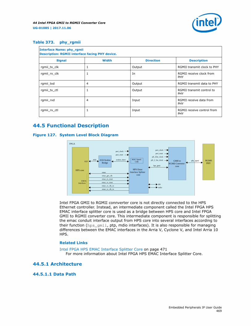
Table 373. phy_rgmii
Interface Name: phy_rgmiiDescription: RGMII interface facing PHY device.
Signal Width Direction Description
rgmii_tx_clk 1 Output RGMII transmit clock to PHY
rgmii_rx_clk 1 In RGMII receive clock fromPHY
rgmii_txd 4 Output RGMII transmit data to PHY
rgmii_tx_ctl 1 Output RGMII transmit control toPHY
rgmii_rxd 4 Input RGMII receive data fromPHY
rgmii_rx_ctl 1 Input RGMII receive control fromPHY
44.5 Functional Description
Figure 127. System Level Block Diagram
HPS Emac Interface Splitter
core
peri_reset
avalon_slave
emac
ptp
mdioemac_tx_clk_in
emac_rx_clk_in
emac_gtx_clk
emac_tx_reset
emac_rx_reset
peri_clock
HPS core
AXI/Avalon Bridge
GMII to RGMII Converter
core
H2FAXI
peri_reset
hps_gmii
pll_25m_clock
peri_clock
RGMII PHY
phy_rgmii
FPGA
MAC Speed CSR
pll_2_5m_clock
EMAC Interfaces
Intel FPGA GMII to RGMII connverter core is not directly connected to the HPSEthernet controller. Instead, an intermediate component called the Intel FPGA HPSEMAC interface splitter core is used as a bridge between HPS core and Intel FPGAGMII to RGMII converter core. This intermediate component is responsible for splittingthe emac conduit interface output from HPS core into several interfaces according totheir function (hps_gmii, ptp, mdio interfaces). It is also responsible for managingdifferences between the EMAC interfaces in the Arria V, Cyclone V, and Intel Arria 10HPS.
Related Links
Intel FPGA HPS EMAC Interface Splitter Core on page 471For more information about Intel FPGA HPS EMAC Interface Splitter Core.
44.5.1 Architecture
44.5.1.1 Data Path
44 Intel FPGA GMII to RGMII Converter Core
UG-01085 | 2017.11.06
Embedded Peripherals IP User Guide469

Figure 128. Data Path Diagram
mac_txd[7:0], mac _txen,mac __txer
mac_tx_clk_o
mac_rst_tx_n
RX Path
rxd_i[7:0], rxdv_i, rxerr _i
mac_rst_rx_n
mac_rx_clk
mac_rxd[7:0], mac _rxdv, mac _rxerr
Soft pipeline with configurable deep
Soft pipeline with configurable deep
TX Path
SDR/DDR Converter
rgmii_txd[3:0],rgmii_txctl
rgmii_rxd[3:0],rgmii_rctl
txd_o[7:0], txen _o,txer _o
mac_col,mac _crs
For transmit path, the GMII/MII data goes through the transmit pipeline register stagebefore going into the SDR/DDR converter block. The pipeline logic can be optionallyenabled or disabled by the user during generation time.
For receive path, the GMII/MII data right after the SDR/DDR converter block goesdirectly to EMAC controller through Intel FPGA HPS EMAC interface splitter core; andalso goes through the receive pipeline register stage. Similarly, this pipeline logic canbe optionally enabled or disabled by the user during generation time.
The SDR/DDR converter block manages single data rate to double data rateconversion and vice-versa. Intel FPGA DDIO component (ALTDDIO_IN andALTDDIO_OUT) is used to perform this task. This block also decodes collision andcarrier sense condition through In-Band status detection.
44.5.1.2 Clock Scheme
44.5.1.2.1 Transmit
All transmit sequential logic in the Intel FPGA GMII to RGMII Converter core is clockedby the HPS PLL during GMII mode (1000 Mbps) and by the FPGA PLL during MII mode(10/100 Mbps).
44 Intel FPGA GMII to RGMII Converter Core
UG-01085 | 2017.11.06
Embedded Peripherals IP User Guide470

Figure 129. Transmit Clocking Scheme
HPS
Clock Manager
Clock Mux in EMAC
Divider and Muxing
FPGA
To the rest of Ethernet Interface
Converter TX Sequential Logic RGMII
PHY
clk_tx_i
GMII
MII
FPGA PLL
25MHz
2.5MHz
rgmii_txcphy_txclk_o
44.5.1.2.2 Receive
All receive sequential logic in the Intel FPGA GMII to RGMII converter core is clockedby rgmii_rx_clk (always driven from the PHY device).
44.6 Intel FPGA HPS EMAC Interface Splitter Core
The Intel FPGA HPS EMAC interface splitter core is used as a bridge between the HPScore and the Intel FPGA GMII to RGMII converter core. It is responsible for splittingthe EMAC conduit interface output from the HPS core into several interfaces accordingto their function (hps_gmii, ptp, mdio interfaces). It is also responsible for managingthe differences between the EMAC interfaces in the Arria V, Cyclone V, and Intel Arria10 HPS. Besides the Avalon-MM slave interface logic, there is no additional real logic inthis core, except it takes the input signals from HPS, regroups them according to theirfunction, and outputs them.
Related Links
Feature Description on page 478
44.6.1 Parameter
44.6.1.1 System Info Parameter
The following parameter is not configurable by the user:
Parameter Description
DEVICE_FAMILY Name: DEVICE_FAMILYIndicates the device family type of the current selected device in Platform Designer.This parameter is used to determine the version of HPS (Arria V, Cyclone V, and Intel Arria 10HPS) supported by the current selected device. This information is used to enable or disablecertain logic; or to terminate certain interfaces of this core.
44.6.1.2 HDL Parameter
44 Intel FPGA GMII to RGMII Converter Core
UG-01085 | 2017.11.06
Embedded Peripherals IP User Guide471

This parameter is not configurable by the user through Platform Designer. Its value isautomatically derived by the component based on the DEVICE_FAMILY parameter.
Parameter Description
Enable mac speed CSR Name: MAC_SPEED_CSR_ENABLE0: The MAC Speed CSR block is not instantiated in this core. In this case, the Mac Speedinformation is directly coming from the HPS EMAC interface.1: The MAC Speed CSR block is instantiated in this core. In this case, the Mac Speedinformation is determined by the control register defined in this core.
44.6.1.3 Intel FPGA HPS EMAC Interface Splitter Core Interface
Figure 130. Intel FPGA HPS EMAC Interface Splitter Core Top Level Interfaces
Intel HPS Emac Interface Splitter
Core
peri_reset
avalon_slave
emac
ptp
mdio
emac_tx_clk_in
emac_rx_clk_in
emac_gtx_clk
emac_tx_reset
emac_rx_reset
peri_clock
hps_gmii
MAC Speed CSR
Table 374. peri_clock
Interface Name: peri_clockDescription: Peripheral clock interface. This interface exists only when the selected device is Arria V or Cyclone
V.
Signal Width Direction Description
clk 1 Input Peripheral clock source usedfor Avalon-MM slaveinterface.
Table 375. peri_reset
Interface Name: peri_resetDescription: Peripheral reset interface. This interface exists only when the selected device is Arria V or Cyclone
V.
Signal Width Direction Description
rst_n 1 Input Active low peripheralasynchronous reset sourceused to reset the Avalon-MMslave interface.This signal is asynchronouslyasserted and synchronouslyde-asserted. Thesynchronous de-assertionmust be provided external tothis core.
44 Intel FPGA GMII to RGMII Converter Core
UG-01085 | 2017.11.06
Embedded Peripherals IP User Guide472
Table 376. avalon_slave
Interface Name: avalon_slaveDescription: This interface exists only when the selected device is Arria V or Cyclone V.
Signal Width Direction Description
addr 1 Input Avalon-MM address bus. (21)
read 1 Input Avalon-MM read control
write 1 Input Avalon-MM write control
writedata 32 Input Avalon-MM write data bus
readdata 32 Output Avalon-MM read data bus
Table 377. emac
Interface Name: emacDescription: Conduit interface connected to HPS EMAC interface
Signal Width Direction Description
phy_txd_o 8 Input GMII/MII transmit data fromHPS
phy_txen_o 1 Input GMII/MII transmit enablefrom HPS
phy_txer_o 1 Input GMII/MII transmit errorfrom HPS
phy_rxdv_i 1 Output GMII/MII receive data validto HPS
phy_rxer_i 1 Output GMII/MII receive data errorto HPS
phy_rxd_i 8 Output GMII/MII receive data toHPS
phy_col_i 1 Output GMII/MII collision detect toHPS
phy_crs_i 1 Output GMII/MII carrier sense toHPS
phy_mac_speed_o 2 Input MAC speed indication fromHPS (22)
mdo_o 1 Input MDIO data output from HPS
mdo_o_e 1 Input MDIO data output enablefrom HPS
mdi_i 1 Output MDIO data input to HPS
ptp_pps_o 1 Input PTP pulse per second fromHPS
ptp_aux_ts_trig_i 1 Output PTP auxiliary timestamptrigger to HPS
(21) The address bus is in the unit of Word addressing.
(22) These bits exist only when the selected device is Intel Arria 10.
44 Intel FPGA GMII to RGMII Converter Core
UG-01085 | 2017.11.06
Embedded Peripherals IP User Guide473

Table 378. emac_gtx_clk
Interface Name: emac_gtx_clkDescription: GMII/MII transmit clock from HPS
Signal Width Direction Description
phy_txclk_o 1 Input GMII/MII transmit clockfrom HPS
Table 379. emac_tx_reset
Interface Name: emac_tx_resetDescription: GMII/MII transmit reset source synchronous to phy_txclk_o from HPS
Signal Width Direction Description
rst_tx_n_o 1 Input GMII/MII transmit resetsource from HPS. Active lowreset.
Table 380. emac_rx_reset
Interface Name: emac_rx_resetDescription: GMII/MII receive reset source synchronous to clk_rx_i from HPS
Signal Width Direction Description
rst_rx_n_o 1 Input GMII/MII receive resetsource from HPS. Active lowreset.
Table 381. emac_rx_clk_in
Interface Name: emac_rx_clk_inDescription: GMII/MII receive clock to HPS
Signal Width Direction Description
clk_rx_i 1 Output GMII/MII receive clock toHPS
Table 382. emac_tx_clk_in
Interface Name: emac_tx_clk_inDescription: GMII/MII transmit clock to HPS
Signal Width Direction Description
clk_tx_i 1 Output GMII/MII transmit clock toHPS
Table 383. hps_gmii
Interface Name: hps_gmiiDescription: GMII/MII interface facing FPGA fabric
Signal Width Direction Description
mac_tx_clk_o 1 Output GMII/MII transmit clockfrom HPS
mac_tx_clk_i 1 Input GMII/MII transmit clock toHPS
continued...
44 Intel FPGA GMII to RGMII Converter Core
UG-01085 | 2017.11.06
Embedded Peripherals IP User Guide474
Interface Name: hps_gmiiDescription: GMII/MII interface facing FPGA fabric
Signal Width Direction Description
mac_rx_clk 1 Input GMII/MII receive clock toHPS
mac_rst_tx_n 1 Output GMII/MII transmit resetsource from HPS
mac_rst_rx_n 1 Output GMII/MII receive resetsource from HPS
mac_txd 8 Output GMII/MII transmit data fromHPS
mac_txen 1 Output GMII/MII transmit enablefrom HPS
mac_txer 1 Output GMII/MII transmit errorfrom HPS
mac_rxdv 1 Input GMII/MII receive data validto HPS
mac_rxer 1 Input GMII/MII receive data errorto HPS
mac_rxd 8 Input GMII/MII receive data toHPS
mac_col 1 Input GMII/MII collision detect toHPS
mac_crs 1 Input GMII/MII carrier sense toHPS
mac_speed 2 Output MAC speed indication fromHPS
Table 384. ptp
Interface Name: ptpDescription: PTP interface facing FPGA fabric
Signal Width Direction Description
ptp_pps_out 1 Output PTP pulse per second toFPGA soft logic
ptp_aux_ts_trig_in 1 Input PTP auxiliary timestamptrigger from FPGA soft logic
ptp_tstmp_data_out 1 Output PTP timestamp data fromHPS to FPGA soft logic
ptp_tstmp_en_out 1 Output PTP timestamp enable fromHPS to FPGA soft logic
44 Intel FPGA GMII to RGMII Converter Core
UG-01085 | 2017.11.06
Embedded Peripherals IP User Guide475

Table 385. mdio
Interface Name: mdioDescription: MDIO interface facing PHY device
Signal Width Direction Description
mdo_out 1 Output MDIO data output to FPGAbidirectional I/O buffer
mdo_out_en 1 Output MDIO data output enable toFPGA bidirectional I/O buffer
mdi_in 1 Input MDIO data input from FPGAbidirectional I/O buffer
Related Links
Avalon-MM Slave Interface on page 477For more information about the Avalon-MM Slave interface, refer to the Avalon-MMSlave interface section.
44.6.1.4 Register
44.6.1.4.1 Register Memory Map
This register block exists only when the selected device is Arria V or Cyclone V. Eachaddress offset represents one word of memory address space.
Name Address Offset Width Attribute Description
CTRL 0x0 2 R/W Control Register
44.6.1.4.2 Register Description
Control Register
Table 386. Control Registers
Bit Fields Access Default Value Description
31:2 Reserved N/A 0x0 Reserved
1:0 MAC_SPEED R/W 0x0 This field indicates thespeed mode used byHPS EMAC and PHYdevice. HPS softwareis required to write tothis field once it hasset the MAC Speed inthe HPS EMAC registerspace after the auto-negotiation process.0x0-0x1: 1000 Mbps(GMII)0x2: 10 Mbps (MII)0x3: 100 Mbps (MII)
44 Intel FPGA GMII to RGMII Converter Core
UG-01085 | 2017.11.06
Embedded Peripherals IP User Guide476

44.6.1.5 Avalon-MM Slave Interface
The following information describes the characteristics of the Avalon slave interface ofthe HPS EMAC interface splitter core:
• Burst width: 32-bit
• Burst support: No
• Fixed read and write wait time: 0 cycle
• Fixed read latency: 1 cycle
• Lock support: No
44.7 Document Revision History
Table 387. Altera GMII to RGMII Converter Core Revision History
Date Version Changes
November 2015 2015.11.06 • Updated "Altera HPS EMAC Interface Splitter Core Interface" PTP table• Updated "Unsupported Features"
July 2014 2014.07.24 Initial release
44 Intel FPGA GMII to RGMII Converter Core
UG-01085 | 2017.11.06
Embedded Peripherals IP User Guide477
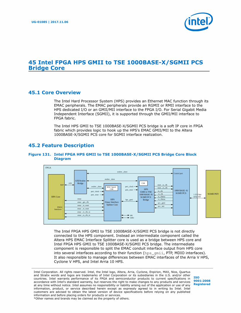
45 Intel FPGA HPS GMII to TSE 1000BASE-X/SGMII PCSBridge Core
45.1 Core Overview
The Intel Hard Processor System (HPS) provides an Ethernet MAC function through itsEMAC peripherals. The EMAC peripherals provide an RGMII or RMII interface to theHPS dedicated I/O or an GMII/MII interface to the FPGA I/O. For Serial Gigabit MediaIndependent Interface (SGMII), it is supported through the GMII/MII interface toFPGA fabric.
The Intel HPS GMII to TSE 1000BASE-X/SGMII PCS bridge is a soft IP core in FPGAfabric which provides logic to hook up the HPS’s EMAC GMII/MII to the Altera1000BASE-X/SGMII PCS core for SGMII interface realization.
45.2 Feature Description
Figure 131. Intel FPGA HPS GMII to TSE 1000BASE-X/SGMII PCS Bridge Core BlockDiagram
HPS Emac Interface
Splitter Core
peri_reset
avalon _slave
emac
ptpmdio
emac _tx_clk_in
emac _rx_clk_in
emac _gtx_clk
emac _tx_reset
emac _rx_reset
peri_clock
HPS Core
AXI/Avalon Bridge
HPS GMII to TSE
1000 BASE -X/SGMII PCS
Bridge
H2FAXI
peri_reset
hps _gmii
peri_clock
SGMII PHY1.25 Gbps serial link
FPGA
MAC Speed CSR
1000 BASE -X/SGMII PCS
avalon _slaveControl port
pcs _gmii
pcs _mii
reset _tx_clk
reset _rx_clk
tx_clk
rx_clk
tx_clkena
rx_clkena
avalon _slave
CSR
EMAC Interfaces
The Intel FPGA HPS GMII to TSE 1000BASE-X/SGMII PCS bridge is not directlyconnected to the HPS component. Instead an intermediate component called theAltera HPS EMAC Interface Splitter core is used as a bridge between HPS core andIntel FPGA HPS GMII to TSE 1000BASE-X/SGMII PCS bridge. The intermediatecomponent is responsible to split the EMAC conduit interface output from HPS coreinto several interfaces according to their function (hps_gmii, PTP, MDIO interfaces).It also responsible to manage differences between EMAC interfaces of the Arria V HPS,Cyclone V HPS, and Intel Arria 10 HPS.
UG-01085 | 2017.11.06
Intel Corporation. All rights reserved. Intel, the Intel logo, Altera, Arria, Cyclone, Enpirion, MAX, Nios, Quartusand Stratix words and logos are trademarks of Intel Corporation or its subsidiaries in the U.S. and/or othercountries. Intel warrants performance of its FPGA and semiconductor products to current specifications inaccordance with Intel's standard warranty, but reserves the right to make changes to any products and servicesat any time without notice. Intel assumes no responsibility or liability arising out of the application or use of anyinformation, product, or service described herein except as expressly agreed to in writing by Intel. Intelcustomers are advised to obtain the latest version of device specifications before relying on any publishedinformation and before placing orders for products or services.*Other names and brands may be claimed as the property of others.
ISO9001:2008Registered

Related Links
Intel FPGA HPS EMAC Interface Splitter Core on page 471
45.2.1 Supported Features
Features supported by the core:
• Enable HPS’s EMAC GMII/MII connection Intel FPGA 1000BASE-X/SGMII PCS core
• Tri-speed (10/100/1000 Mbps) operation
• Dynamic speed switching
45.3 Core Architecture
45.3.1 Data Path
Figure 132. Transmit Data Path
mac _txd[7:0], mac _txen ,mac _txer
tx_d[7:0], tx_en ,tx_err
TX Elastic Buffer
GMII port
tx_d[3:0], tx_en ,tx_err
MII port
1000 BASE -X/SGMII PCS
GMII/MII port
HPS
For transmit path, the GMII/MII data from the HPS goes through the transmit elasticbuffer before going into the PCS GMII and MII port. The transmit elastic buffer isresponsible for handling slight frequency differences between the transmit clock fromHPS and the transmit clock generated from the PCS’s block.
Figure 133. Receive Data Path
mac _rxd[7:0], mac _rxdv,mac _rxer
gmii_rx_d[7:0], gmii_rx_en ,gmii_rx_err
GMII port
{mii_rx_d[3:0],mii_rx_d[3:0]}, mii_rx_en ,mii_rx_err
MII port
1000 BASE -X/SGMII PCS
GMII/MII port
HPS
mac _speed [1]
The PCS block has separate GMII and MII ports while the HPS has only single GMIIand MII ports. Therefore a mux is needed in the receive data path. During MII mode,the 4 bits MII receive data bus is duplicated in order to feed 8 bits to the GMII/MIIreceive data bus of HPS. The mac_speed information from the HPS or from the CSR inIntel FPGA HPS EMAC Interface Splitter core is used as mux select.(23)(24)
45 Intel FPGA HPS GMII to TSE 1000BASE-X/SGMII PCS Bridge Core
UG-01085 | 2017.11.06
Embedded Peripherals IP User Guide479

45.3.2 Clock Scheme
During GMII mode (1000 Mbps), both the HPS and PCS blocks generate a transmitclock. The GMII/MII data from the HPS is synchronous to the HPS’s internal PLL whilethe PCS block expects transmit data to be synchronous to its own transmit clock. Tosolve two different transmit clocks in a transmit data path, an elastic buffer is used fortransmit data transmission.
During MII mode (10/100 Mbps), a transmit clock only comes from the PCS block. Thetransmit clock connected to the HPS is the gated version of transmit clock sent fromPCS block with the worst duty cycle of 1% (high: 4 ns, low: 396 ns).
The receive clock comes from the PCS block. The receive clock connected to the HPSis the gated version of receive clock sent from the PCS block with worst duty cycle of1% (high: 4 ns, low: 396 ns).
45.3.3 MAC Speed
Mac speed information is used to select different transmit clock sources.
Arria V or Cyclone V HPS cores do not provide mac speed information to the FPGAfabric. Therefore a control register is defined in the Intel FPGA HPS EMAC InterfaceSplitter corefor software to configure it correctly according to the speed used by HPSEMAC and PHY device.
The Intel Arria 10 HPS provides mac speed information to the FPGA fabric. The controlregister in the Intel FPGA HPS EMAC Interface Splitter core is automatically removed.
The two incoming mac_speed bits going into Intel FPGA HPS GMII to TSE 1000BASE-X/SGMII PCS bridge is treated as asynchronous and static. Only 1 bit(mac_speed[1]]) is being used to determine whether the MAC is operating in GMII orMII mode. Therefore a double synchronizer is enough to synchronize (mac_speed[1]).No additional filtering logic is needed unless both bits are used.
45.3.4 Transmit Elastic Buffer
Transmit elastic buffer is asynchronous FIFO with fix high and low watermark level.High watermark level is fixed at (TX_BUFFER_DEPTH/2 + 4) valid entries and lowwatermark level is fixed at (TX_BUFFER_DEPTH/2 - 4) valid entries. When the numberof valid entries is equal or above the high watermark level, any IDLE symbolappearing at the write port of the buffer is dropped (IDLE symbol deletion). When thenumber of valid entries is equal or below low watermarks level, any IDLE symbol readfrom the read port does not increment the read pointer of the buffer (IDLE symbolinsertion). IDLE symbol definition is tx_en = 0 and tx_err = 0.
The buffer depth is fixed at 64. Higher buffer depths provides more margins to avoidoverflow/underflow condition to occur. The buffer depth configuration depends on themaximum Ethernet packet or maximum IDLE symbol separation in the Ethernetprotocol and the maximum ppm different between the two clock sources.
(23) Avalible for Cyclone V and Arria V SoC devices.
(24) Avalible for Intel Arria 10 SoC devices.
45 Intel FPGA HPS GMII to TSE 1000BASE-X/SGMII PCS Bridge Core
UG-01085 | 2017.11.06
Embedded Peripherals IP User Guide480

Figure 134. Elastic Buffer Watermark Level
default write pointer position
High watermark (TX_BUFFER _DEPTH /2 + 4)
TX_BUFFER _DEPTH -1
default read pointer position
0
TX_BUFFER _DEPTH /2
Low watermark (TX_BUFFER _DEPTH /2 - 4)
almost full threshold
almost empty threshold
45.3.4.1 GMII to MII Mode Transition
The elastic buffer works when both write and read ports are having an equal or similarclock frequency. Ethernet operation allows dynamic speed mode changes. During aGMII to MII or MII to GMII mode transition, there could be a possibility that thetransmit clock from HPS clock source and PCS block are out of sync in terms of clockfrequency. If they are out of sync this causes an overflow/underflow condition tooccur.
For example, during GMII to MII mode transition, the transmit clock from the PCScould be running at 25/2.5MHz while clock switching in HPS may yet to be completedand running at 125MHz. Clock switching in the PCS and HPS could incur a short periodof an inactive clock as well due to graceful clock mux implementation. This challengeis handled through software.A register bit which act as a soft reset to the buffer isdefined in this adapter core. Software is responsible to ensure the buffer is disabledwhen there is a change in the speed configuration of the PCS and MAC. The buffer isenabled only when configuration in both PCS and MAC blocks are completed and avalid transmit clock is running at both read and write ports of the buffer.
45.3.5 Avalon-MM Slave Interface
The following are the configuration of the Avalon-MM slave interface:
• Bus width: 32-bit
• Fixed read and write wait time: 0 cycles
• No burst support
• No lock support
45.3.6 Programming Model
Software is required to disable and enable the transmit data path accordinglywhenever there is change in speed mode configuration.
In the case of Cyclone V and Arria V SoC devices, software is required to program themac_speed register in Intel FPGA HPS EMAC Interface Splitter core as per MAC or PHYdevice setting.
45 Intel FPGA HPS GMII to TSE 1000BASE-X/SGMII PCS Bridge Core
UG-01085 | 2017.11.06
Embedded Peripherals IP User Guide481
Refer to the Triple-Speed Ethernet IP Core User Guide for programming sequence ofthe MAC and PCS block respectively.
Related Links
Triple-Speed Ethernet MegaCore Function User Guide
45.4 Configuration Parameters
45.5 Interface
Figure 135. Intel FPGA HPS GMII to TSE 1000BASE-X/SGMII PCS Bridge Top LevelInterfaces
HPS GMII to TSE 1000 BASE -X/SGMII PCS Bridge
peri_reset
hps _gmiipcs _gmii
pcs _mii
peri_clock pcs _transmit _reset
pcs _receive _reset
pcs _transmit _clock
pcs _clock_enable
pcs _receive _clockavalon _slave
Table 388. Top Level I/O Port List
Signal Width Direction Description
Interface Name: peri_clockDescription: Peripheral clock interface
clk 1 Input Peripheral clock source
Interface Name: peri_resetDescription: Peripheral reset interface
rst_n 1 Input Active low peripheral asynchronous reset source.This signal is asynchronously asserted and synchronously de-asserted. Thesynchronous de-assertion must be provided external to this core.
Interface Name: avalon_slaveDescription: Avalon MM slave interface for CSR access of this core
addr 1 Input Avalon-MM address bus. The address bus is in the unit of word addressing.
read 1 Input Avalon-MM read control
write 1 Input Avalon-MM write control
writedata 32 Input Avalon-MM write data bus
readdata 32 Output Avalon-MM read data bus
Interface name: hps_gmii
continued...
45 Intel FPGA HPS GMII to TSE 1000BASE-X/SGMII PCS Bridge Core
UG-01085 | 2017.11.06
Embedded Peripherals IP User Guide482
Signal Width Direction Description
Description: Conduit interface connected to HPS EMAC GMII/MII interface
mac_tx_clk_o 1 Input GMII/MII transmit clock from HPS
mac_tx_clk_i 1 Output GMII/MII transmit clock to HPS
mac_rx_clk 1 Output GMII/MII receive clock to HPS
mac_rst_tx_n 1 Input GMII/MII transmit reset source from HPS. Active low reset.
mac_rst_rx_n 1 Input GMII/MII receive reset source from HPS. Active low reset.
mac_txd 8 Input GMII/MII transmit data from HPS
mac_txen 1 Input GMII/MII transmit enable from HPS
mac_txer 1 Input GMII/MII transmit error from HPS
mac_rxdv 1 Output GMII/MII receive data valid to HPS
mac_rxer 1 Output GMII/MII receive data error to HPS
mac_rxd 8 Output GMII/MII receive data to HPS
mac_col 1 Output GMII/MII collision detect to HPS
mac_crs 1 Output GMII/MII carrier sense to HPS
mac_speed 2 Input MAC speed indication from HPS
Interface name: pcs_transmit_resetDescription: Transmit reset source from HPS
pcs_rst_tx 1 Output Inverted version of mac_rst_tx_n. Active high reset.
Interface name: pcs_receive_resetDescription: Receive reset source from HPS
pcs_rst_rx 1 Output Inverted version of mac_rst_rx_n. Active high reset.
Interface name: pcs_transmit_clockDescription: Transmit clock from PCS block
pcs_tx_clk 1 Input Transmit clock from PCS block.
Interface name: pcs_receive_clockDescription: Receive clock from PCS block
pcs_rx_clk 1 Input Receive clock from PCS block
Interface name: pcs_clock_enableDescription: Transmit and receive clock enabler from PCS block
pcs_txclk_ena 1 Input Transmit clock enabler from PCS block. This signal enables the pcs_tx_clk.
pcs_rxclk_ena 1 Input Receive clock enabler from PCS block. This signal enables the pcs_rx_clk.
Interface name: pcs_gmiiDescription: GMII interface to the PCS block
pcs_gmii_rx_dv 1 Input Receive data valid from PCS block
pcs_gmii_rx_d 8 Input Receive data from PCS block
pcs_gmii_rx_err 1 Input Receive data error from PCS block
pcs_gmii_tx_en 1 Output Transmit data enable to PCS block
continued...
45 Intel FPGA HPS GMII to TSE 1000BASE-X/SGMII PCS Bridge Core
UG-01085 | 2017.11.06
Embedded Peripherals IP User Guide483
Signal Width Direction Description
pcs_gmii_tx_d 8 Output Transmit data to PCS block
pcs_gmii_tx_err 1 Output Transmit data error to PCS block
Interface name: pcs_miiDescription: MII interface to the PCS block
pcs_mii_rx_dv 1 Input Receive data valid from PCS block
pcs_mii_rx_d 4 Input Receive data from PCS block
pcs_mii_rx_err 1 Input Receive data error from PCS block
pcs_mii_tx_en 1 Output Transmit data enable to PCS block
pcs_mii_tx_d 4 Output Transmit data to PCS block
pcs_mii_tx_err 1 Output Transmit data error to PCS block
pcs_mii_col 1 Input Collision detect from PCS block
pcs_mii_crs 1 Input Carrier sense from PCS block
45.6 Registers
45.6.1 Register Memory Map
Each address offset represent one word of memory address space.
Table 389. Control Register Memory Map
Register Address Offset Width Attribute
CTRL 0x0 1 R/W
45.6.2 Register Description
Table 390. Control Register (CTRL)
Bit Fields Access Default Value Description
31:1 Reserved N/A 0x0 Reserved
0 TX_DISABLE R/W 0x1 Transmit data pathdisable bit.This field disables thetransmit data path ofthe adapter core. Itacts as software resetto all transmitsequential logic in theadapter core (examplethe elastic buffercontroller).1: Transmit data pathis disabled (default).0: Transmit data pathis enabled.
45 Intel FPGA HPS GMII to TSE 1000BASE-X/SGMII PCS Bridge Core
UG-01085 | 2017.11.06
Embedded Peripherals IP User Guide484

45.7 Document Revision History
Table 391. Altera HPS GMII to TSE 1000BASE-X/SGMII PCS Bridge Core
Date Version Changes
May 2017 2017.05.08 Initial release
45 Intel FPGA HPS GMII to TSE 1000BASE-X/SGMII PCS Bridge Core
UG-01085 | 2017.11.06
Embedded Peripherals IP User Guide485

46 Intel FPGA MSI to GIC Generator Core
46.1 Core Overview
In the PCI subsystem, Message Signaled Interrupts (MSI) is a feature that enables adevice function to request service by writing a system-specified data value to asystem-specified message address (using a PCI DWORD memory write transaction).System software initializes the message address and message data during deviceconfiguration, allocating one or more system-specified data and system-specifiedmessage addresses to each MSI capable function.
A MSI target (receiver), Intel FPGA PCIe RootPort Hard IP, receives MSI interruptsthrough the Avalon Streaming (Avalon-ST) RX TLP of type MWr. For Avalon-MM basedPCIe RootPort Hard IP, the RP_Master issues a write transaction with the system-specified message data value to the system-specified message address of a MSI TLPreceived. This memory mapped mechanism does not issue any interrupt output tohost the processor; and it relies on the host processor to poll the value changes at thesystem-specified message address in order to acknowledge the interrupt request andservice the MSI interrupt. This polling mechanism may overwhelm the processorcycles and it is not efficient.
The Intel FPGA MSI-to-GIC Generator is introduced with the purpose of allowing levelinterrupt generation to the host processor upon arrival of a MSI interrupt. It exists asa separate module to Intel FPGA PCIe HIP for completing the interrupt generation tohost the processor upon arrival of a MSI TLP.
46.2 Background
The existing implementation of the MSI target at Intel FPGA PCIe RootPort translatesthe MSI TLP received into a write transaction via PCIe Hard IP Avalon-MM Master port(RP_Master). No interrupt output directed to the host processor to kick start theservice routine for the MSI sender is needed.
46.3 Feature Description
The Intel FPGA MSI-to-GIC Generator provides storage for the MSI system-specifieddata value. It also generates level interrupt output when there is an unread entry. Thefollowing figure illustrates the connection of the MSI-to-GIC Generator module in aPCIe subsystem.
UG-01085 | 2017.11.06
Intel Corporation. All rights reserved. Intel, the Intel logo, Altera, Arria, Cyclone, Enpirion, MAX, Nios, Quartusand Stratix words and logos are trademarks of Intel Corporation or its subsidiaries in the U.S. and/or othercountries. Intel warrants performance of its FPGA and semiconductor products to current specifications inaccordance with Intel's standard warranty, but reserves the right to make changes to any products and servicesat any time without notice. Intel assumes no responsibility or liability arising out of the application or use of anyinformation, product, or service described herein except as expressly agreed to in writing by Intel. Intelcustomers are advised to obtain the latest version of device specifications before relying on any publishedinformation and before placing orders for products or services.*Other names and brands may be claimed as the property of others.
ISO9001:2008Registered

Figure 136. MSI-to-GIC Generator in PCIe RP system
HostProcessor
MSI-to-InterruptGenerator
PCIe RPHIP
Level IRQ RP_Master/Host Master to
Avalon-MM Slave Data Port
Host Master to Avalon-MM
Slave CSR Port
This module is connected to RP_Master of PCIe RootPort HIP issuing memory mapwrite transaction upon MSI TLP arrival. System-specified data value carried by the MSITLP is written into the module storage. The same Avalon MM Data Slave port alsoconnects to the host processor for MSI data retrieval upon interrupt assertion. An IntelFPGA MSI-to-GIC Generator module could contain data storage from one to 32 wordsof continuous address span. Each data word of storage is associated with acorresponding numbered bit of Status Bits and Mask Bits registers. Each data wordaddress location can store up to 32 entries.
There is an up to 32-bit Status Register that indicates which storage word location hasan unread entry. Also, there is a similar bit size of Interrupt Mask Register that is inplace to allow control of module behavior by the host processor. The Interrupt Maskregister provides flexibility for the host processor to disregard the incoming interrupt.
The base address assigned for Intel FPGA MSI-to-GIC Generator module in thesubsystem should cover the system-specified message address of MSI capablefunctions during device configuration. Multiple Intel FPGA MSI-to-GIC Generatormodules could be instantiated in a subsystem to cover different system-specifiedmessage addresses.
Avalon-MM Slave interfaces of this module honors fixed latency of access to ensurethe connected master (in this case, the RP_Master) can successfully write into themodule without back pressure. This avoids the PCIe upstream traffic from impactbecause of backpressuring of RP_Master.
Since MSI is multiple messages capable and multiple vectors are supported by eachMSI capable function, there is a tendency that a system-specified message addressreceives more than one MSI message data before the host processor is able to servicethe MSI request. The Component is configurable to have each data word address toreceive up to 32 entries, before any data value is retrieved. When you reach themaximum data value entry of 32, subsequent write transactions are dropped andlogged. This ensures every write transaction to the storage has no back pressurewhich may lead to system lock up.
46.3.1 Interrupt Servicing Process
46 Intel FPGA MSI to GIC Generator Core
UG-01085 | 2017.11.06
Embedded Peripherals IP User Guide487
When a new message data is written inIntel FPGA MSI-to-GIC Generator module, thestorage word associated Status bit is set automatically and a level interrupt output isthen fired. The host processor that receives this interrupt output is required to servicethe MSI request, as indicated in the following procedure:
1. The host processor reads the Status Register to recognize which data wordlocation of its storage is causing the interrupt.
2. The host processor reads the firing data word location for its system-specifiedmessage data value sent by the MSI capable function. Upon reading the dataword, message data is considered consumed, the associated Status bit is thenunset automatically. If the word location entry is empty, then the Status bit stillremains asserted.
3. The host processor services either the MSI sender or the function who calls for theMSI.
4. Upon completing the interrupt service for the first entry, the host processor maycontinue to service the remaining entry if there is any residing inside the wordlocation, by observing the associated Status bit.
5. The host processor may run through the Status Register and service each firingStatus bit in any order.
46.3.2 Registers of Component
The following table illustrates the Intel FPGA MSI-to-GIC Generator registers map asobserved by the host processor from its Avalon-MM CSR interfaces. The bit size ofeach register is numbered according to the configured number of data word storagefor MSI message of the component. The maximum width of each register should be 32bits because the configurable value range is from 1 to 32.
Table 392. CRA registers map
Word Address Offset Register/ Queue Name Attribute
0x0 Status register R
0x1 Error register RWNote: Write '1' to clear
0x2 Interrupt Mask register RW
46.3.2.1 Status Register
The status register contains individual bits representing each of the data wordslocation entry status. An unread entry sets the Status bit. The Status bit is clearedautomatically when entry is empty. The value of the register is defaulted to ‘0’ uponreset.
The following table illustrates the Status register field.
46 Intel FPGA MSI to GIC Generator Core
UG-01085 | 2017.11.06
Embedded Peripherals IP User Guide488
Table 393. Status Register fields
Field Name Bit Location
Status bit for message data word location [31:1] 31:1
Status bit for message data word location [0] 0
46.3.2.2 Error Register
The Error register bit is set automatically only when the associated message dataword location that contains the write entry, indicating it was dropped due to maximumentry limit reached. The Error bit indicates the possibility of the MSI TLP targeting theassociated system-specified address. This condition should not happen as each MSIcapable function is only allowed to send up to 32 MSI even with multiple vectorsupported.
The Error bit can be cleared by the host processor by writing ‘1’ to the location.
Upon reset, the default value of the Error register bits are set to ‘0’.
The following table illustrates the Pending register field.
Table 394. Error Register fields
Field Name Bit Location
Error bit for message data word location [31:1] 31:1
Error bit for message data word location [0] 0
46.3.2.3 Interrupt Mask Register
The Interrupt Mask register provides a masking bit to individual Status bit before theStatus is used to generate level interrupt output. Having the masking bit set,disregards the corresponding Status bit from causing interrupt output.
Upon reset, the default value of Interrupt Mask register is 0, which means every singledata word address location is disabled for interrupt generation. To enable interruptgeneration from a dedicated message entry location, the associated Mask bit needs tobe set to ‘1’.
The following table illustrates the Interrupt Mask register field.
Table 395. Interrupt Mask Register fields
Field Name Bit Location
Masking bit for Status [31:1] 31:1
Masking bit for Status [0] 0
46.3.3 Unsupported Feature
46 Intel FPGA MSI to GIC Generator Core
UG-01085 | 2017.11.06
Embedded Peripherals IP User Guide489
The message data entry Avalon-MM Slave represents the system-specified address forMSI function. The offset seen by MSI function should be similar to the offset seen bythe host processors. As this Avalon-MM Slave interface is accessible (write and read)by both the host processor and the PCIe RP HIP, any read transaction to the offsetaddress (system-specified address) is considered to have the message data entryconsumed. Observing this limitation, only host master, which is expected to serve theMSI should read from the Avalon-MM Slave interface. A read from the PCIe RP_Masterto the Avalon-MM Slave is prohibited.
46.4 Document Revision History
Table 396. Altera MSI to GIC Generator Core Revision History
Date Version Changes
July 2014 2014.07.24 Initial release
46 Intel FPGA MSI to GIC Generator Core
UG-01085 | 2017.11.06
Embedded Peripherals IP User Guide490

A Document Revision HistoryThis section covers the revision history of the entire volume. For details regardingchanges to a specific chapter refer to each chapter revision history.
Table 397. Embedded Peripherals IP User Guide Volume Revision History
Date Version Changes
November 2017 2017.11.06 • Removed the Supported Devices topic from various cores. Refer toDevice Support.
December 2016 2016.12.19 Maintenance release.
October 2016 2016.10.28 New chapters:• Altera Avalon I2C (Master) CoreUpdated:• 16550 UART Core• Altera I2C Slave to Avalon-MM Master Bridge Core
June 2016 2016.06.17 New chapters:• Avalon-MM DDR Memory Half Rate Bridge CoreUpdated chapters:• UART Core• SPI Core• Altera Interrupt Latency Counter Core• Altera I2C Slave to Avalon-MM Master Bridge Core
May 2016 2016.05.03 New chapters:• Altera I2C Slave to Avalon-MM Master Bridge CoreUpdated chapters:• Vectored Interrupt Controller Core
December 2015 2015.12.16 Removed chapters:• PCI Lite Core• Avalon-ST JTAG Interface CoreUpdated chapters:• 16550 UART Core• PIO Core• Altera Modular Scatter-Gather DMA Core
November 2015 2015.11.06 Removed chapters:• Mailbox Core-Replaced with Intel FPGA Avalon Mailbox Core on page
102Updated chapters:• 16550 UART Core• Avalon-ST Bytes to Packets and Packets to Bytes Converter Cores• Altera Modular Scatter-Gather DMA Core• Vectored Interrupt Controller Core• Altera GMII to RGMII Adapter Core• Altera Avalon Mailbox (simple) Core
June 2015 2015.06.12 New chapters:continued...
UG-01085 | 2017.11.06
Intel Corporation. All rights reserved. Intel, the Intel logo, Altera, Arria, Cyclone, Enpirion, MAX, Nios, Quartusand Stratix words and logos are trademarks of Intel Corporation or its subsidiaries in the U.S. and/or othercountries. Intel warrants performance of its FPGA and semiconductor products to current specifications inaccordance with Intel's standard warranty, but reserves the right to make changes to any products and servicesat any time without notice. Intel assumes no responsibility or liability arising out of the application or use of anyinformation, product, or service described herein except as expressly agreed to in writing by Intel. Intelcustomers are advised to obtain the latest version of device specifications before relying on any publishedinformation and before placing orders for products or services.*Other names and brands may be claimed as the property of others.
ISO9001:2008Registered

Date Version Changes
• Altera Quad SPI Controller Core• Altera Serial Flash Controller Core• Altera Avalon Mailbox Core• Altera GMII to RGMII Adapter CoreUpdated chapters:• 16550 UART Core• Performance Counter Core• DMA Controller Core• PIO Core• Interval Timer CoreThe following chapters have been reinserted:• Avalon-ST Single-Clock and Dual-Clock FIFO Cores• Avalon Streaming Channel Multiplexer and Demultiplexer Cores• Avalon-ST Round Robin Scheduler Core• Avalon-ST Delay Core• Avalon-ST Splitter Core• Avalon Streaming Test Pattern Generator and Checker Cores• Avalon Streaming Data Pattern Generator and Checker CoresThe following chapters have been removed:• Common Flash Interface Controller Core• Cyclone III Remote Update Controller Core (No longer available starting
from V14.0)
A Document Revision History
UG-01085 | 2017.11.06
Embedded Peripherals IP User Guide492