embedded system project (521423s) - university of · pdf fileembedded system project (521423s)...
TRANSCRIPT

Embedded System Project (521423S)
Juha RöningAntti Tikanmäki
Anssi Kemppainen

About the course
• The goal of this course is to help students understand the world of embedded computer systems by developing an embedded system.
• Usually participants are information and electrical engineering students who are specialized in software and system design.
• The Embedded System Project is related to but independent of Embedded Software Project (Sulautettujen ohjelmistojen projekti, 521275A) that concentrates on software-hardware interface.
• A project like assignment that requires approximately 120-160 hours from a team of three students.
• This course is structured as a guided walk through the hardware design process.
– Consists of the beginning lecture and five meetings with the assistant
– Each meeting is after one design phase. The previously done work is checkedand the next phase explained in each meeting.

About the course
In this course students:
• Go through complete design and implementation process of a device
• Do formal requirement specification and technical specification
• Select and order suitable components for the device
• Create schematics, layout and manufacturing files for PCB
• Populate PCB and test the board
• Design and implement software for the device
• Do formal testing to verify that the device fill the requirements
• Write documentation (during whole process)

Project phases

Design phases
In practice:
1. Requirement specification, Technical
specification, test plan, Schedule
2. Schematics, component ordering
3. Layout and manufacturing files, PCB
ordering
4. Populating the board and electrical
testing
5. Programming software and testing
6. Final demonstration and Final report
System requirements
Sketch of software
Sketch of hardware
Evaluation and simulation against requirements
Detailed HW-design
Test design
PWB and assembly
Software
HW-tests Simulator tests
Integration
operation procedures
modes, functions, algorithms, control
testability considerations
embedded software design
EEPROM programming
power consumption, environment etc.
partitioning, basic solutions
schematics and layout
printed wiring board manufacturing
continuity and HW functionality

Phase 1: Planning
Requirement specification
• List of features
– Figure out what is the purpose and required functions of your device
• Numerical requirement (like storage, power, time of operation)
– For example: logging 10 hours of motor temperatures from 4 places twice in a
second to SD card
-> You will find requirements for memory, storage, power usage, calculation
speed, size of device,…
– You need to have numerical requirements when selecting for example
temperature sensor from 1365 options available in digikey
• Use numbering and hierarchy:
– Req_1: User interface,
– Req_1.1: operating buttons, …
– Req_2: Measuring temperature

Phase 1: Planning
Technical specification
• Study AVR application notes and component datasheets
• Technical solution for ReqSpec
• Component comparison and choices
• Select Microcontroller that contains suitable features (like I2C,SPI,…)
– In this course, prefer 8bit AVR MCUs
• Calculations of values
• Define size of passive components
• Try to have only one voltage, like 5V or 3.3V if possible.
• Read through datasheets of selected components, especially for controller!
– Try to use build in functionalities, like uart,spi, i2c, adc, …
• Select components that are available in stock and reasonable price
• Software specification

Phase 1: Planning
Test plan
– How to verify that each requirement is filled
• Calibration? Reference measurement?
• Example: temperature measurement with reference device
– How to test that technical solutions works as expected
– If minimum and maximum requirement exist, how to measure in these conditions
– Use same reference numbering as in previous documents
Schedule
– Reserve weekly hours that you are able/will spend on this project
– Deadlines for each phase to complete project in time
• Define what needs to be done before DL
– Continuously update LOG of used hours to learn how much time each job is
taking in practice in design process
– Keep your time schedule
• If schedule is missed, do rescheduling
– Report progress in week-reports

Phase 2: Schematics, component ordering
Information sources:
• The datasheets of components
• Study Atmel Application notes
• "typical application“ from datasheets
Practical schema design issues:
• Know what is a pullup or pulldown resistor
• Use filtering capacitors
• How to regulate operating voltage
• Don’t forget testing points (HW)
• Never connect any output directly to the ground or power supply
Some tips:
• Use comments on schema to clarify solutions
• When technical specification is complete, group is allowed to order components
• Use component order list provided in course web page
Tools:
• Kicad http://www.kicad-pcb.org/

Phase 3: Layout and manufacturing files, PCB
ordering
Layout:
• Aim for short tracks to avoid inductance disturbances
• You can use SMD components
• Route your board with such a principle that you use top layer for vertical tracks and
bottom layer for horizontal tracks. Or vice versa.
• Clear routes help on debugging
• Place the filter capacitors of IC components as close as possible to the IC:s Vcc and
Gnd pins.
• Choose the track width according the average current that goes through it.
• Remember test pins
• Connect the extra copper of your board to ground

Phase 3: Layout and manufacturing files, PCB
ordering
Manufacturing files:
• After drawing a layout, print it as a 1:1 size print and try if the components fits
• Run Design Rule Check (DRC) against given parameters
• Check Gerber files with Kicad’s Gerber view program
PCB ordering (when permission given by Assistant):
• Manufacturing at our own workshop
• Manufacturing in FABLAB CNC
• If you want to have your own boards: Order from China for example from:
http://imall.iteadstudio.com/open-pcb/pcb-prototyping.html
10 pieces 50x50mm at 9.90 $

Phase 4: Populating the board and electrical
testing
• Hand operated SMD pick and place manipulator for populating the board in FABLAB
• For physical measurement of electrical features
– Oscilloscopes
– Multimeters
• Measure all soldering for short circuits before connecting the power
• For powering up the device
– DC power sources
– Batteries
• Testing
– Work systematically
– Use scope to test availability of signals
– To test some of the functionalities, you need software routines

Phase 5: Software
Software design:
• Develop the software parallel to hardware, especially separate testing routines for
verifying that hardware is working correctly
• You may use C or C++, if very time critical is involved, use assembly
• You may use open source libraries / functions to get devices working
• Design SW timing, like how many times in second something is done
Coding:
• Split software to modules. For example SPI.c, I2C.c, X_sensor.c
• Main.c should contain only high level function calls and main loop
• Design use of interrupts and polling
• Don’t write too long functions
• Study what is meaning of const, struct, volatile, pointers and how to use eeprom
• Study how globals works in practice
• Decide variable types (unsinged or signed? 8,16 or 32 bits? Floats?)
• Use struct pointers in function calls instead of many parameters
• You can measure your software timing in practice by using extra mcu pins and scope

Tools: Software development and debugging
environmentFor software developing and debugging• Windows: with Atmel-Studio IDE and WinAVR compiler (avr-gcc)• Linux: Atmel AVR toolchain
• AVR JTAG ICE Emulator
• The self-made PCB contains an MCU with a JTAG interface for connecting to AVR JTAG ICE. The MCU contains an on-chip debug block, which is used for debugging. ICE connects to this block via JTAG interface.
• The software is uploaded to the Flash memory of an MCU with AVR JTAG ICE and ran normally.
• The on-chip debug block allows debugging the software similarly to PC: stepping the code, reading variable values, break points, etc. Additionally, all the registers of the MCU are available for modifying.
• When software works properly with AVR JTAG ICE, power off the device, disconnect AVR JTAG connector and you are ready to run the device independently. No further software uploads are necessary because the software is always ran in MCU.
PCB
MCU
Flash
memory
O
C
D
Core
Other
blocks
JTAG-
conne
ctor
AVR
JTAG
ICE
PC
- AVR-
Studio
IDE
- WinAVR
compiler
USB
emulator cable

Course procedure

Course procedure
• Send e-mail to assistant ([email protected]) containing who areyour group members. Your assistant (Antti or Anssi) will reply to you givingyou a group number
• Name all your documents and e-mail messages with your group number
– Group1_technical_specification.pdf, etc.
• First face-to-face meeting should be in 2-3 weeks after the start. Otherwisemany students are tempted to delay their full commitment, resulting in largedelays in completion.
Each group needs to send short weekly report using email containing
progress and next things to do to prove that work is progressing as scheduled

Course procedure
• The assistant will have at least 5 scheduled 15-30 minute meetings with each group.
• Send documents to be reviewed one day before the meeting
• During the meetings the teams will describe their solutions, ideas and encounteredproblems, helping the assistant to correct serious design flaws at an early stage.
• The meetings also encourage to the planned use of time, instead of painful around-the-clock marathons as the deadline approaches.
• The contents of the meetings is as follows:
1. Inspection of requirement and implementation specification, and timetable.Advice on schematics and component list for students.
2. Inspection of the schematics, component order list and inspection of refinedspecifications. Advice on layout for students.
3. Inspection of layout printed in 1:1 scale. Footprint check and permission formanufacturing the PCB.
4. Inspection of an assembled board. Advice on the emulator and AtmelStudio usefor students.
5. Demonstration of working board. Documentation and board left for grading.

Deliverables
1. Specification document containing– Requirement specification
– Implementation specification
– Test plan
2. Project plan
– Schedule– log of work process
3. Schematic and layout of the PCB
4. Software
5. A prototype of the device and demonstration
6. Final report containing– Device description
– User manual
– Test report
– Overall description of the implementation and future development
At the end, send all documents as zip file for complete review and grading

Grading
Grading is based on
• Documentation (on each Phase)
• Board design
– How well the given design guidelines are used
• The sanity of the design (schematics check: pullups, filtering, hazardous connections)
• Some jump wires will not affect to the grading. The students must be able to
experiment.
• The number of created board versions will not be considered, since it
consumes so radically time to make another iteration of a board.
• Inspection against requirements
– Check each requirement
– Assessment of the stability of the system
• Keeping of the schedule
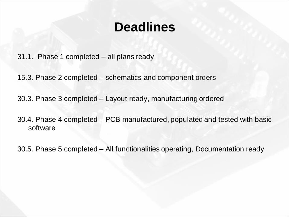
Deadlines
31.1. Phase 1 completed – all plans ready
15.3. Phase 2 completed – schematics and component orders
30.3. Phase 3 completed – Layout ready, manufacturing ordered
30.4. Phase 4 completed – PCB manufactured, populated and tested with basic software
30.5. Phase 5 completed – All functionalities operating, Documentation ready

Lectures
3 times to give practical tips for each project phase:
16.01. ma 14.15-16.00 Specifications, TS128
23.01. ma 14.15-16.00 Schematics, layout, TS128
30.01. ma 14.15-16.00 Software and testing, TS128
06.02. ma 14.15-16.00 Software and testing, TS128
Each lecture contains 10-15 minutes briefing lecture, and after that free discussion
related to own projects

Topics

About the topic
The basic requirements:
• meant for people that are new to the embedded systems.
• contains only familiar technologies and the teachers are familiar with the topic,enabling more efficient tutoring
• some suitable components for the assignment have been pre-examined, letting thestudents to avoid the full exposure to “navigation” problems, such as selecting,finding, and ordering components
Other features:
• The teams are free to create additional features to their system if they will.
• These additional features affect positively (to a certain extend) to the grading of the
team
Own topics:
• meant for students with some experience in embedded systems
• Students suggest a subject, assistants help refine it, and professor accepts it.
• If you want the PCB after the course ends, you must buy the main components.
Addition to basic topic, some special research related topics may be available on
course web page within few weeks after course start day

Aihe 1: Langaton kiihtyvyys/kallistusanturi
• Ominaisuudet:
– 9Dof IMU-sensori
• LSM9DS1 breakout board: https://www.sparkfun.com/products/13284
• MPU-9250 breakout board: https://www.sparkfun.com/products/13762
– akku ja latauspiiri
– radio: joko BTLE-, WLAN- tai UWB-radio
– käyttöliittymän napit ja ledit / näyttö / visualisointi
• Sovellusvaihtoehdot johon opiskelijat toteuttavat:
– Aktiivisuusranneke
– asentotiedon mittaus (kiinnitetään esim. kameraan)
– ihmisen pään asennon mittaus (kiinnitetään päähän)
– Urheilusovellus, esim. mailan asento

Aihe 1: Langaton kiihtyvyys/kallistusanturi
• Lisäoptiona voi toteutatta jonkin tai useamman näistä:
– BTLE- tai UWB-perusteisen yksinkertaisen paikannuksen
– IR-lähettimeen + ulkoisiin kameroihin perustuva paikannus
– servon/moottorin tai muun mekaanisen laitteen ohjaus laitteen
avulla
– Ohjelmisto, joka integroi paikkaa 9dof avulla
– langaton lataus
– pikalataus esim. superkonkkaan
• Olennaista työssä on myös (työn arvosanaan vaikuttaa):
– Analysoida, mitata ja demonstroida järjestelmän viive
– optimoida käyttöaika suhteessa laitteen kokonaispainoon

Aihe 2: langaton paineanturi
kosketuspisteen ja voiman mittaamiseen
Ominaisuudet:
• käyttää joustavia resistiivisiä tai kapasitiivisia antureita
• web- tai mobiilikäyttöliittymä, jossa visualisoituna voima ja piste
Esim. sovelluskohteita:
• integroituna vaatteiseen (hiha, hanskan selkä) toteuttamaan
käyttöliittymiä
• integroituna jääkiekkokypärän sisälle mittaamaan törmäysten
voimaa

Aihe 3: Bioloid-robotti
Dynamixel AX-12A -servomoottorit
- UART
- Tehtävä uusi ohjain ja ohjelmistorajapinta
Muut ominaisuudet:
- Omat anturit
- uSD-muisti ohjelmistolle
- WLAN / BT
- Näyttö
Loppudemonstraatio testiradalla:
- Pari yksinkertaista estettä
MCU:
- Joko 8bit tai 32bit AVR
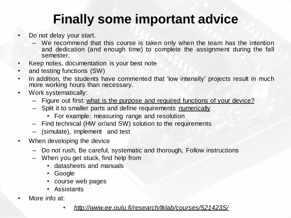
• Do not delay your start.
– We recommend that this course is taken only when the team has the intentionand dedication (and enough time) to complete the assignment during the fallsemester.
• Keep notes, documentation is your best note
• and testing functions (SW)
• In addition, the students have commented that ‘low intensity’ projects result in muchmore working hours than necessary.
• Work systematically:
– Figure out first: what is the purpose and required functions of your device?
– Split it to smaller parts and define requirements numerically
• For example: measuring range and resolution
– Find technical (HW or/and SW) solution to the requirements
– (simulate), implement and test
• When developing the device
– Do not rush, Be careful, systematic and thorough, Follow instructions
– When you get stuck, find help from
• datasheets and manuals
• course web pages
• Assistants
• More info at:
• http://www.ee.oulu.fi/research/tklab/courses/521423S/
Finally some important advice