emerging nvm technologies in main memory for energy
TRANSCRIPT

HAL Id: lirmm-02135043https://hal-lirmm.ccsd.cnrs.fr/lirmm-02135043
Preprint submitted on 20 May 2019
HAL is a multi-disciplinary open accessarchive for the deposit and dissemination of sci-entific research documents, whether they are pub-lished or not. The documents may come fromteaching and research institutions in France orabroad, or from public or private research centers.
L’archive ouverte pluridisciplinaire HAL, estdestinée au dépôt et à la diffusion de documentsscientifiques de niveau recherche, publiés ou non,émanant des établissements d’enseignement et derecherche français ou étrangers, des laboratoirespublics ou privés.
Emerging NVM Technologies in Main Memory forEnergy-Efficient HPC: an Empirical Study
Abdoulaye Gamatié, Alejandro Nocua, Joel Weloli, Gilles Sassatelli, LionelTorres, David Novo, Michel Robert
To cite this version:Abdoulaye Gamatié, Alejandro Nocua, Joel Weloli, Gilles Sassatelli, Lionel Torres, et al.. EmergingNVM Technologies in Main Memory for Energy-Efficient HPC: an Empirical Study. 2019. �lirmm-02135043�
DRAFT REPORT, MAY 2019 1
Emerging NVM Technologies in Main Memory forEnergy-Efficient HPC: an Empirical Study
Abdoulaye Gamatie, Alejandro Nocua, Joel Wanza Weloli, Gilles Sassatelli,Lionel Torres, David Novo, and Michel Robert
Abstract—The spectrum of scientific disciplines wherecomputer-based simulation and prediction play a central roleis broad: biology, medicine, high energy physics, climatology,astronomy, etc. In the near future, expected exascale supercom-puters will make it possible to address scientific problems thatare more complex than ever. However, a major challenge onthe path to such supercomputers is the required high energy-efficiency, i.e., maximizing the amount of computational workper watt.
To answer this challenge, the position of this paper relies oncompute nodes built from inherently low-power technologies. Itconsiders 64-bit ARM processors combined with emerging non-volatile memory (NVM) technologies for main memory, knownto be a bottleneck regarding performance and energy. DRAMtechnology is until now the mainstream option for main memory.However, it will hardly scale beyond a certain level becauseincreased DRAM capacity requires higher refresh rates, whichis harmful to power consumption. In such a context, emergingNVMs have become promising alternatives to DRAM thanks totheir memory cell density and negligible leakage. This paper eval-uates the impact of various main memory technologies, namelyDDR4 SDRAM, Phase-Change Memory (PCM), Resistive RAM(RRAM), on computing system performance and memory-relatedenergy consumption. The obtained results show that RRAM isa very promising candidate to mitigate main memory energyconsumption, while PCM tends to represent a better candidate forstorage level. Compared to DDR4 SDRAM, we observe RRAMcan provide comparable system-level performance, while themain memory energy consumption can be reduced by up to 50%.
Index Terms—Memory architecture, nonvolatile memory,phase change memory, resistive RAM, DRAM, multicore process-ing, high-performance computing, low-power electronics, systemsimulation, performance evaluation
I. INTRODUCTION
EXASCALE computing [1] is a key enabler for addressingsome of the grand challenges of mankind in areas such as
medicine, sustainability and climatology. Exascale is set as thenext milestone in every supercomputing roadmap, albeit oftenpostponed because of several scalability challenges amongwhich target power consumption.
Exascale computers should be capable to perform 1018 float-ing point operations per second (flops), within a reasonablepower budget, typically below 20 MW. The general designchallenges related to these computers concern various aspectsincluding processor, memory and interconnect technologies,
A. Gamatie, A. Nocua, G. Sassatelli, L. Torres, D. Novo, and M. Robertare with CNRS and University of Montpellier - LIRMM laboratory, France(e-mail: [email protected]).
J. Wanza Weloli is with Bull, Atos Technologies, France (e-mail:[email protected]).
as well as programming models. The present study focuseson compute node designs, i.e. building blocks for exascaleparallel computers, based on ARM processors [2] combinedwith emerging non volatile memory (NVM) technologies [3].These processors are usually energy-efficient, while emergingNVMs have inherently a negligible leakage that contributes todrastically reduce the overall power consumption in computenodes.
A. A glance at ARM SoCs for compute nodes
ARM-based Systems-on-Chip (SoCs) are known to pro-vide a good power and performance compromise. Thanks tothe generalization of 64-bit ARMv8 ISA alonside significantprogress on micro-architecture and software stack, they havebecome attractive for high-performance computing (HPC)applications [2].
ThunderX2 processor. Among the latest solutions, we canmention the Marvell’s ThunderX2 processor, which supportsARMv8.1 architecture [4]. This chip has 8 memory channels,delivering theoretically up to 33% more memory bandwidththan its equivalent the Intel’s Skylake processor as the latterfeatures only 6 DDR4 memory channels [5]. This translatesinto 33% better performance on HPCG [6] and memory-boundapplications. The ThunderX2 processor has been recentlycompared with others x86 processors including Skylake [7].Overall, it provides similar performance level compared toSkylake. It is slower when executing compute-bound high-performance applications due to its inherent lower floating-point throughput. In fact, it does not feature vector unitscontrarily to Intel Advanced Vector Extensions (AVX-512) [5].
SPARC64 XIfx processor. The A64FX CPU is the Fu-jitsu’s SPARC64 XIfx (sparc architecture) ARM-based highperformance CPU successor [8]. Manufactured in 7nm pro-cess TSMC technology, it is compliant with the ARMv8.2-Aspecification. It is the first CPU that implements the 512-bitARM Scalable Vector Extension (SVE), designed specificallyfor high performance computing [9]. It includes 48 workercores in addition to 4 helper cores (2 I/O and 2 system) Itcan perform up to 2.7 teraflops for 64-bit (FP64) operationsand more than 80% of the 1TB/s theoretical memory peakbandwidth delivered by four High Bandwidth Memory (HBM)blocks [9]. Floating point performance is about 35% higherthan the top-of-the-line Xeon Skylake CPUs.
Kunpeng 920 processor. Recently, the Huawei’s Kunpeng920 has been announced as the ”highest-performance ARM-based CPU” [10], exceeding A64FX. Manufactured also in

DRAFT REPORT, MAY 2019 2
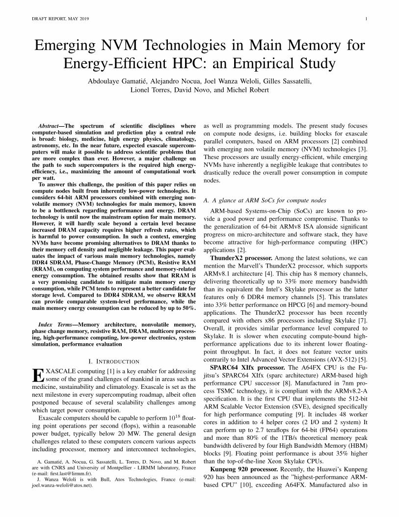
Fig. 1: A realistic ARM-based chip design
7nm, this chip integrates 64 cores at a frequency of 2.6 GHzand 8 DDR4-2933 channels. The Kunpeng 920 processor hason-board couterments including two NIC 100G RoCE fornetworking and a support for PCIe Gen4 and CCIX interfaces.Details about the ARM core architecture are not public yet,except the fact that the gains come from an optimization ofbranch prediction algorithms, a higher number of operationunits, alongside an improved memory subsystem architecture.
While the intrinsic compute energy-efficiency of the aboveARM SoCs in terms of flops/W is very promising, the globalefficiency at compute node level must also consider othercrucial components such as memory. In particular, main mem-ory plays a central role regarding the efficient data access. Ithas a direct impact on the overall system performance andenergy-efficiency. This is true in both embedded and high-performance computing domains.
EXAMPLE 1 (A REALISTIC COMPUTE NODE DESIGN): TheEuropean Montblanc projects1 have been exploring the designof ARM-based supercomputers for exascale computing. Arealistic compute node design in this context is shown inFigure 1. It includes ARMv8 core clusters with a three-levelcache memory hierarchy, i.e. L3, L2 and L1 levels.
The corresponding SoC has 4 HBM stacks that provideup to 48GB of on-package memory. It consists of 2 dies (orchiplets) on a passive interposer, connected through high speedCCIX links and four stacks of on-chip DRAM. AdditionalDRAM memory controllers compatible with emerging NVMtechnologies are envisioned in order to improve the memorycapacity. This floorplan indicates the potential of addingfurther IPs such as multi-channel NVM controllers, powermanagement cores or accelerators, to exploit the silicon areaof the chiplet (improving their utilization rate). However, oneneed to balance the trade-off of adding the new IPs, withrespect to the SoC power budget.
1https://www.montblanc-project.eu
Generally, memory and I/O related macros are typicallyplaced at the edge due to mainstream package integrationtechnology requirements. Memory PHYs are wide structurestaking significant area at the edge of the SoC. Both availableedge space due to target SoC dimensions and availablepackage pin count determine the number of memory interfacesthat can be included.
B. The main memory bottleneck
A number of notable trends have been identified in theliterature about main memory [11]. Modern systems keep onintegrating several processing units, which can be heteroge-neous (e.g., CPUs, GPUs or FPGA) in order to fulfill the re-quirements of performance-demanding applications. Followingthis trend, a drop by 30% of the memory capacity per core isenvisioned every two years [12]2. Therefore, per-core memorybandwidth will decrease.
DRAM technology will further hardly scale beyond a cer-tain technology node, because of higher cell manufacturingcomplexity, reduced reliability, and rising cell leakage [13].In addition, increased DRAM capacity inevitably requireshigher refresh rates. The energy consumed by off-chip memoryhierarchy, including DRAM, memory controller and theirconnecting interfaces, can reach up to 41% of the total energyconsumption of a compute system [14]. In addition, the refreshmechanism of DRAM induces power consumption even whenno activity occurs in the memory. For instance, authors in [15]evaluated the increase in performance and power overheadsdue to refresh in high-density 32Gb memory devices.
The background power consumption related to the periph-eral circuitry, e.g., word-line drivers, sense-amplifiers andwrite drivers, represents another concern as it contributessignificantly to the memory leakage. They observed that
2To the best of our knowledge, no updated projection is provided in theliterature regarding this trend since [12].
DRAFT REPORT, MAY 2019 3
refresh can account for more than 20% of the DRAM energyconsumption while running SPEC CPU2006 benchmarks witha full-system simulator. The background energy consumptionis the largest part of the overall energy reported for eachmemory size.
DEFINITION 1 (ADDRESSED PROBLEM): We focus on thepower consumption issue of DRAM-based main memory, re-lated to their refresh and peripheral circuitry requirements.We seek cost-effective solutions that can adequately overcomethis issue, without incurring neither performance penalty norimportant integration efforts in compute systems.
Typically, considering the reference design shown in Figure1, one would like to combine low-latency and high-bandwidthon-chip HBM memory with off-chip memories to extend theper core main memory capacity at least up to 2GB (requiredfor HPC applications). In this specific case, we have to feedall cores with 128GB of main memory in total. However, wecan only provide 96GB with the on-chip HBM blocs. Then,32GB of off-chip memory are required. We have two possiblechoices: i) either integrate the latest DDR5 technology (DDR5-4400), or ii) integrate a custom low power and multi-channelNVM module.
C. Non volatile memory technologies
1) Making the case for NVM: To support our motivation toselect NVMs as candidate solutions for the aforementionedproblem, Table I introduces some numbers regarding theirmain characteristics [3]. We selected two very promising NVMtechnologies3: Resistive RAM (RRAM) and Phase ChangeMemory (PCM). The table provides a relative comparisonbasis that will serve to assess the specific memory models usedin the rest of this paper. One must keep in mind that generallyat system level, the interconnect used for memory access hasa notable (if not the highest) impact on those metrics.
TABLE I: Approximate device-level characteristics of NVMs
DRAM Non Volatile MemoryRRAM PCM
Cell size (F2) 6 4 - 10 4 - 12Read latency (nsec) ∼10 ∼10 20 - 60Write latency (nsec) ∼10 ∼50 20 - 150
Read energy medium low mediumWrite energy medium high high
Leakage power medium low lowWrite endurance > 1015 108 - 1011 108 - 109
Maturity mature test chips test chips
Among the most relevant features of NVMs for energy-efficiency, we note their low leakage power. Since they arenon volatile, they do not require any data refresh mecha-nism to maintain written values in the memory, contrarily toDRAM. NVMs enable to store multiple bits per cell, whichleads to higher density. However, writing operation on thoseNVMs is more expensive compared to DRAM. Unlike charge-based memories, NVMs store data in the material structure
3Spin Transfer Torque RAM (STT-RAM) [16] is another candidate technol-ogy, which is unconsidered in this work. In the framework of the MontBlanc3project, it has been rather considered for the cache level hierarchy as addressedin [17], [18], and in particular at the last-level cache.
or properties (resistive switching memories). Accordingly, awrite operation involves changing cell’s physical state andthus consumes more time and energy than a read operation.Furthermore, NVM cells often withstand a much smallernumber of write operations before wearing out. As writeendurance of NVMs is critical for most technologies, therehave been significant efforts over the last years to mitigate thisissue, e.g., by minimizing / avoiding memory writes via silentstores elimination [19], [20], by adopting advanced cachereplacement policies [21], by applying memory mappings thataccount for NVM retention time [22], and by improvingthe technology itself [23]. Even though wear-leveling is aprominent concern for emerging NVMs, the current study willmainly focus on performance and energy concerns.
The main memory market, though extremely competitive,is a promising application area for Non-Volatile Memories(NVMs) from different perspectives:
• Technology independence: main memory comes in formof discrete memory modules made of chips with a JEDECDDR standardized interface, thereby lifting the difficultyof integrating different technologies on the same sub-strate.
• Voiding refresh needs: DRAM consumes a significantamount of energy into the necessary refresh cycles. Theoverall resulting complexity of DRAM required for cop-ing with the hierarchical organization in pages, ranks andbanks incurs significant performance penalties comparedto NVMs. Indeed, thanks to their inherent non-volatility,most NVMs do not require any refresh mechanism topreserve their stored data. This also confers to NVMnegligible leakage.
• Scaling and density NVM memory technologies canscale better than DRAM. For instance, the Phase-ChangeMemory is expected to scale to 9nm around 2022, whilea 20nm prototype was already proposed in 2008 byIBM [11]. This enables denser memories that could meetthe memory capacity requirements of multi/manycorecompute systems.
2) A brief overview of PCM and RRAM technologies: ThePCM memory technology was first proposed in 1970 [24] byGordon Moore, co-founder of Intel. However, material qualityand power consumption issues prevented commercializationof the technology until very recently. A number of indus-trial actors already announced PCM-based device prototypes(e.g., Samsung, Toshiba, IBM and SK Hynix [25]). Morerecently, Intel and Micron announced the 3D XPoint NVMtechnology [26], which shares many similarities with the PCMtechnology. However, details of the materials and physicsof operation have not been fully disclosed. A 375GB SSDPCIe card from Intel, aimed at enterprise markets, is goingto be released as the first product with this technology in2019. Both PCM and 3D XPoint technologies are regarded aspotential solutions for a compromise between main memoryand storage-class memory. Their higher access latencies anddynamic power consumption compared to DRAM (see TableI) may however become penalizing at main memory level.
The RRAM memory technology [27] dates back to 2003,
DRAFT REPORT, MAY 2019 4
when Unity Semiconductor started developing its ConductiveMetal-Oxide (CMOx) technology. This technology works byvarying the resistance across a dielectric solid-state material.The RRAM technology has proved a promising candidate formain memory thanks to its lower power consumption andaccess latency compared to PCM (see Table I). It has demon-strated a good stability at 10nm node [27]. Among outstandingindustrial players investing in the RRAM technology, one canmention Panasonic Semiconductor [28].
D. Our contribution
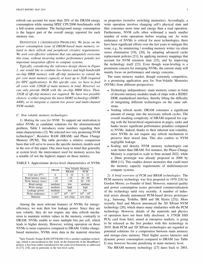
In this paper, we explore the impact of integrating emergingNVMs in ARM Compute Nodes to enable energy-efficienthigh-performance computing. An initial version of this workcan be found in a report [29]. The proposed design analysisis achieved by adopting two simulation tools: the gem5 [30]cycle-approximate architecture simulator coupled with theNVMain main memory simulator [31].
We calibrate a DRAM model based on a Micron DDR4datasheet [32]. We also build new PCM and RRAM memorytechnology models, starting from NVMain models that arefurther refined based on an analysis of the existing literature onNVMs. Our evaluation targets state-of-the-art heterogeneousARMv8 multicore systems, envisioned for better processingefficiency of compute nodes in upcoming HPC systems. Theexplored system designs are validated on typical applicationworkloads.
Our results show that RRAM is a very good candidatefor energy issue mitigation at main memory level, whilePCM would be a more promising candidate for storage level.We show that RRAM can provide system-level performancecomparable to DDR4, while memory energy consumption canbe reduced by up to 50%. This is not the case of PCM.
E. Outline of paper.
The remainder of this paper is organized as follows: Sec-tion II presents some related work on NVM integration atmain memory level; then, Section III describes our designexploration framework; Section IV evaluates the performanceand energy consumption of a compute node system modelintegrating different memory technologies at main memory.The aim is to confirm the relevance of NVM for energyimprovement; Section V focuses on a few main memorysystem design choices aiming at demonstrating how the energygains expected from NVM integration could be further im-proved; Section VI discusses some gained insights and brieflydeals with the open question about the programmability ofcompute nodes integrating NVMs in main memory; finally,some closing remarks are given in Section VII.
II. RELATED WORK
We describe some existing studies promoting emergingNVM technology at main memory level. These studies consid-ered different main memory architectures like NVM-uniformor hybrid DRAM-NVM.
A. NVM-uniform main memory architectures
Lee et al. [33] examine the use of PCM to completelyreplace DRAM as main memory. They architect a PCM-based main memory system that helps mitigating the negativeimpact of high write energy and latency. For this purpose, theyused more and smaller row buffers to improve locality andwrite coalescing. To address the write endurance issue, theyproposed tracking and writing only modified data to the PCMdevice. These initial results show that performance, energyand endurance of PCM chips can be greatly improved withthe proposed techniques.
In addition, one can achieve more efficient designs ofNVM chips by taking advantage of the non-destructive natureof reads, which enables simpler and narrower row bufferorganizations [34]. Unlike in DRAM, an entire NVM memoryrow does not need to be buffered by a device because reading amemory row does not destroy the data stored in the row. Mezaet al. [34] showed that having narrow row buffers in emergingnon-volatile devices can greatly reduce main memory dynamicenergy compared to a DRAM baseline with large row sizes.This happens without greatly affecting memory endurance.And, for some NVM technologies, it can lead to improvedperformance.
Existing work often promote PCM and RRAM for mainmemory due to their smaller cell size. Nevertheless, a fewstudies also explored the opportunities offered by other emerg-ing NVMs such as the Spin Transfer Torque RAM (STT-RAM) [16]. For instance, Kultursay et al. [35] draw similarconclusion as Lee et al. [33] upon evaluation of the completereplacement of DRAM with STT-RAM. To tackle the longwrite latency and high write energy problems of STT-RAM,they proposed an architecture that selectively writes back thecontents of the row buffer when it is modified. The architectureonly writes back a data that is modified to reduce writeoperation energy and latency. In addition, to improve thelocality of accesses to STT-RAM, they propose bypassing themodification of the row buffer for write operations. With thesuggested modifications, the STT-RAM based main memoryshows to be more energy-efficient than a DRAM-based mainmemory.
B. Hybrid DRAM-NVM architectures
Yoon et al. [36] make the key observation that row buffersare present in both DRAM and PCM. And, these row buffershave (or can be designed to have) the same latency and band-width in both DRAM and PCM. Yet, row buffer misses aremuch more costly in terms of latency, bandwidth, and energyin PCM than in DRAM. To exploit this, they devise a policythat avoids accessing in PCM data that frequently causes rowbuffer misses. Hardware or software can dynamically keeptrack of such data and allocate/cache it in DRAM whilekeeping data that frequently hits in row buffers in PCM. PCMalso has much higher writing cost than reading cost. To takethis into account, the allocation/caching policy is biased suchthat pages that are more likely written stay in DRAM.
Ware et al. [37] recently propose a hybrid DIMM archi-tecture combining DRAM and a modified Flash with reduced

DRAFT REPORT, MAY 2019 5
Fig. 2: Main memory organization in NVMain-gem5 simulation flow.
read latencies. They claimed their proposal was commerciallyrealizable. They evaluated the performance and endurance fordata-center workloads. The obtained results showed that thecombination can enabled 88% of the performance of a DRAM-only system of the same capacity at 23% of the cost.
Other work has examined how to reduce latency, energy,and cost of managing the metadata required to locate data ina large DRAM cache in hybrid main memories [38], [39]. Suchmetadata is typically stored in SRAM in traditional CPU cachearchitectures. In this work, Meza et al. made the observationthat only a limited amount of data is accessed with highlocality in a large DRAM cache and only a small amountof metadata needs to be kept to locate data in the cache. Bydistributing metadata within the DRAM cache itself (see [38])and by employing their technique, the authors show similarperformance to storing full cache metadata can be achievedwith smaller storage size.
C. Merging main memory and storageEmerging NVM memory technologies offer the possibility
of designing systems and applications that can manipulatepersistent data directly in memory, instead of going througha slow storage interface. In fact, if we keep the traditionaltwo-level memory/storage model in the presence of these fastNVM devices as part of storage, the operating system and filesystem code for locating, moving, and translating persistentdata from the non-volatile NVM devices to volatile DRAMbecomes a great bottleneck.
Meza et al. [40] show that operating system and file systemcode causes most of the memory energy consumption anddegrade performance by an order of magnitude in some data-intensive workloads. To avoid such overhead, they proposea persistent memory manager. It consists of a hardware ac-celeration unit that coordinates and unifies memory/storagemanagement in a single address space that spans potentiallymultiple different memory technologies (DRAM, NVM, flash)via hardware/software cooperation.
Another related challenge includes the design of systemresources that can concurrently handle applications/access-patterns that manipulate persistent data as well as those thatmanipulate non-persistent data. For example, Zhao et al. [41]address the problem of designing effective memory schedul-ing policies in the presence of these two different types ofapplications/access-patterns.
III. DESIGN EXPLORATION FRAMEWORK
We describe the setup of our modeling and evaluationframework. As mentioned in the introductory section, we com-
bine the gem5 and NVMain tools to carry out our design eval-uations. The gem5 simulator provides an accurate evaluationof system performance thanks to its high configurability fora fine-grained ARM architecture modeling [42] [43]. Its full-system simulation mode runs unmodified operating systems.It includes several predefined architecture component models,e.g., CPU, memory and interconnect. This simulator producesdetailed execution statistics at the micro-architecture level.NVMain [31] is an architectural-level simulator that enablesto evaluate main memory designs, as illustrated in Figure 2.It is flexible enough to allow the implementation of variousmemory controllers, interconnects and organizations. It is well-integrated together with the gem5 simulator, which makes itpossible to simulate a variety of main memory technologies ina system. Among existing micro-architecture simulators thatmodel NVM-based memory systems in detail, NVMain isthe most advanced one to best of our knowledge. State-of-the-art simulators like DRAMSim2 [44], DRAMSys [45] andRamulator [46] rather focus on DRAM technology modeling.
It is worth-mentioning that the results presented in this paperare obtained with a full-system cycle-level simulation of theconsidered benchmarks and applications. This is considerablydemanding in terms of simulation effort and results for mostexperiments in weeks of simulation on a manycore server.We believe it is necessary to gather relevant insights thatfully take into account the micro-architectural features of thedesigned systems. Existing approaches [37] adopts reasonablesimplifications by either simulating workload traces (in placeof the full code) or selecting some representative portions ofan application.
In the sequel, starting from the selected memory technolo-gies, we briefly describe the considered evaluated multicoreheterogeneous architecture.
A. Evaluated system designThe memory models used in our study are indicated in
Table II. They are designed based on a DDR4 model fromMicron [32], a PCM model defined by Samsung [47] and aRRAM model defined by Panasonic [48] (see Sections III-A1and III-A2). While the DDR4 model has been completely de-rived from the corresponding data-sheet provided by Micron,the two NVM models have been enhanced according to an in-depth review of the literature. These models are considered asinputs by NVMain to estimate delays and energy consumptionof the main memory while executing various workloads.
Table II indicates for each considered memory model thenumber of channels, banks, ranks and interface frequenciesused in our evaluations.
DRAFT REPORT, MAY 2019 6
TABLE II: Compared 4GB main memory configurations
Name (Channel, Bank, Rank) Interf. freq. [MHz]DDR4 Micron [32] (2,4,2) 1333PCM Samsung [47] (2,1,2) {400, 1333}
RRAM Panasonic [48] (2,4,2) {400, 1333}
1) DDR4 Technology Modeling: As a reference for ourstudy, we consider the DRAM technology used in the CaviumThunderX2 compute nodes of the Dibona supercomputer builtby Atos/Bull, within the MontBlanc 3 H2020 European project(see https://www.montblanc-project.eu/prototypes). This tech-nology consists of a DDR4 from Micron defined from thecorresponding data-sheet [32]. The bandwidth of the referencememory module considered for our investigation is around21.3GB/s according to the data-sheet.
2) NVM Technology Modeling: First of all, we note thatbuilding realistic models of PCM and RRAM technologiesis not a trivial task since only a few prototype designs arecurrently available. The design parameters of these prototypesare hardly available. A few NVM performance and energyevaluation tools [49] [50] could be considered as an alternativesolution. Unfortunately, they fail to provide the fine-grainparameter description necessary to main memory modeling.For all these reasons, we decided to rely our study on the PCMand RRAM models provided by NVMain. They respectivelyresult from Samsung [47] and Panasonic [48] specifications,presented in the International Solid-State Circuits Conference(ISSCC’20124), the top venue for presenting the most ad-vanced memory prototypes. While the latency parameters areconsistent with the designs from Samsung and Panasonic, itis not the case of the energy parameters.
We, therefore, modified the values of energy parameters inorder to get as close as possible to the featured NVMs. Thedetailed parameter values will be found in the appendix of ourinitial report [29]. We extrapolated the NVM energy parametervalues according to existing literature on NVM [51] [52] [3].In particular, we considered the following energy ratios, w.r.t.the above DDR4 model as the DRAM reference:
• 2.1x and 43.1x more energy-consuming for read and writeon PCM respectively;
• 1.2x and 23.7x more energy-consuming for read and writeon RRAM respectively.
On the one hand, the above ratios considered for PCM resultfrom [51] in which authors carried out an exhaustive analysisof a number of PCM prototypes proposed in literature from2003 to 2008. We assume these ratios remain relevant enoughfor the Samsung PCM model proposed in 2012 and integratedwithin NVMain. Note that these ratios may have been reducedtoday with recent advances in PCM.
4To the best of our knowledge, these are the most complete modelspublically available for NVM evaluation at main memory level. In addition,the recent trends about NVMs observed in the literature suggest that therelative comparison between these technologies has not changed.
It is worth-mentioning that since 2012, state-of-the-art on NVMtechnologies has noticeably evolved. Therefore, the ISSCC’2012 modelsconsidered in the current study should be considered as a pessimisticapproximation basis, meaning that nowadays NVM designs might enablefurther gains.
On the other hand, the ratios concerning the RRAM havebeen chosen empirically from the trends found in NVM-relatedliterature [52] [3], which suggests that RRAM has bit-leveldynamic energy that is comparable to DRAM. However, interms of latency, writes are several times slower than reads.So, we assume that the write energy on RRAM is notablyhigher compared to DRAM, while it remains lower than forPCM. In fact, the recent trends about RRAM suggest that thistechnology has at least the same energy cost in read comparedto DRAM, while the gap in write energy is getting reducedbetween the two technologies. Therefore, the value ratioschosen above can be seen as an upper-bound approximationthat allows us to conduct a conservative analysis in the rest ofthis document. In other words, there exists a probable marginfor improving the quantified gains reported in this work.
The maximum write bandwidths originally specified by theauthors of the previous NVM models are 40MB/s for a 8GbPCM [47] and 443MB/s for a 8Mb RRAM [48]. In the presentwork, an identical number of devices is used for both NVMand DDR4 models: 8 devices. Moreover, 256-bits and 512-bitsrow buffers are respectively considered for PCM and RRAMmodels. More details about the other parameters of consideredmemory architectures will be found in the appendix of [29].Given this setup, we observed that the write bandwidths ofthe PCM and RRAM models can reach up to 400MB/s and1500MB/s respectively, when running an application like theHigh Performance Conjugate Gradient (HPCCG) [6].
3) Heterogeneous multicore architecture: We consider theExynos 7420 ARMv8 chip embedded in the Exsom board [53]for modeling our simulated architecture in gem5. This chiprelies on the big.LITTLE technology proposed by ARM. TableIII summarizes the main parameters of the architecture.
For the sake of convenience, in the remainder of this paper,we rely on the aforementioned 8-cores ARMv8 multicorearchitecture as a simple instance of larger scale ARMv8 high-performance compute nodes. This enables a reasonable gem5-NVMain co-simulation cost in the conducted experimentswhile still enabling to stress the memory subsystem. To givean idea of the overall complexity related to the experimentscarried out in our current study, gem5-NVMain co-simulationshave been run on a private 64 cores local server for about twomonths.
B. Setup validation
As a preliminary evaluation, we focus on intrinsic propertiesof the modeled main memories: access latency and idle powerconsumption. We aim at assessing the soundness of the basememory models decided in Section III.
Given the accepted relative modeling of the NVMs energyparameters (i.e. ratios w.r.t. DRAM energy) described inSection III-A2, we decided to present all our design evaluationresults in the form of normalized metrics, with DDR4 as thereference for comparison. We believe absolute metric valuesare less relevant here. In fact, the adoption of normalizedperformance metrics is a standard practice in NVM-basedliterature for unbiased analysis [37] [33] [34] [35] [36] [40]because of the frequent relative modeling of their parameters.

DRAFT REPORT, MAY 2019 7
TABLE III: Exynos 7 Octa (7420) SoCs characteristics and corresponding gem5 models
Exynos 7 Octa (7420) ex7 gem5 model
ParametersCortex-A53ARMv8 ISA
(in-order)
Cortex-A57ARMv8 ISA
(out-of-order)
ex7 LITTLE(in-order)
ex7 big(out-of-order)
Max. core count 4 4 4 4Frequency 1.4GHz 2.1GHz 1.5GHz 2.1GHz
L1ISize 32kB 48kB 32kB 48kB
Assoc. 2 3 2 3Latency 3 3 3 3
L1DSize 32kB 32kB 32kB 32kB
Assoc. 4 2 4 2Latency 3 3 3 3
L2Size 256kB 2MB 256kB 2MB
Assoc. 16 16 16 16Latency 12 16 12 16
Interconnect CCI-400 XBAR - 256 bus width @533MHzMemory 4GB DDR4@1333MHz, 2 channels see Table II
Memory bus width 64 64Technology 14nm FinFET -
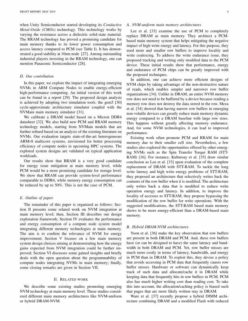
1) Memory Latency: We consider the lmbench benchmarksuite [54] to assess the read latency of each memory tech-nology. In particular, we use the lat mem rd benchmark tomeasure the memory hierarchy latency when using a DDR4,PCM and RRAM in main memory. Note that the L1 and L2caches are both in SRAM. Basically, the memory hierarchylatency is computed by repeatedly accessing contiguous datastructures of increasing sizes, given a particular value ofmemory stride length. In our experiments, we consider a stridelength of 4kB. The result of these repetitive computations arevariations in memory access latency, according to its hierarchylevels: L1 cache, L2 cache, and main memory.
Fig. 3: Memory latency with various technologies.
The result provided by lat mem rd is reported in Figure 3(here, the plotted latency values follow a logarithmic scale).The X-axis, denoted as ”Array Size”, represents the memoryobject sizes (in kB) for which the read latencies (in ns)are determined by the benchmark. The benchmark has beenexecuted while using a single LITTLE core with 32kB L1cache, 256kB L2 cache, and 4GB main memory. The memoryinterface frequency (i.e., the I/O bus clock) of the DDR4memory model is 1333MHz, while the memory interfacefrequencies of PCM and RRAM are set to 400MHz accordingto the initial configuration inherited from NVMain original
Fig. 4: Idle memory energy consumption.
setup.As expected, Micron’s DDR4 model offers a better memory
latency compared to both RRAM and PCM. Their respectivemain memory latencies are nearby 69 nsec, 383 nsec, and 813nsec. In other words, read accesses in the considered DDR4model are respectively 5.5 and 11.7 times faster in comparisonwith RRAM and PCM respectively.
Comparing these results w.r.t. the tendencies usually foundin the literature (see Table I), we observe that the device-level slowdown of PCM in read latency compared to RRAMand DRAM is confirmed. However, this is not the case forRRAM compared to DRAM: while the read latencies of thetwo memory technologies are similar at device level, it is notthe case at memory system level. Indeed, read accesses withDDR4 are faster than with RRAM.
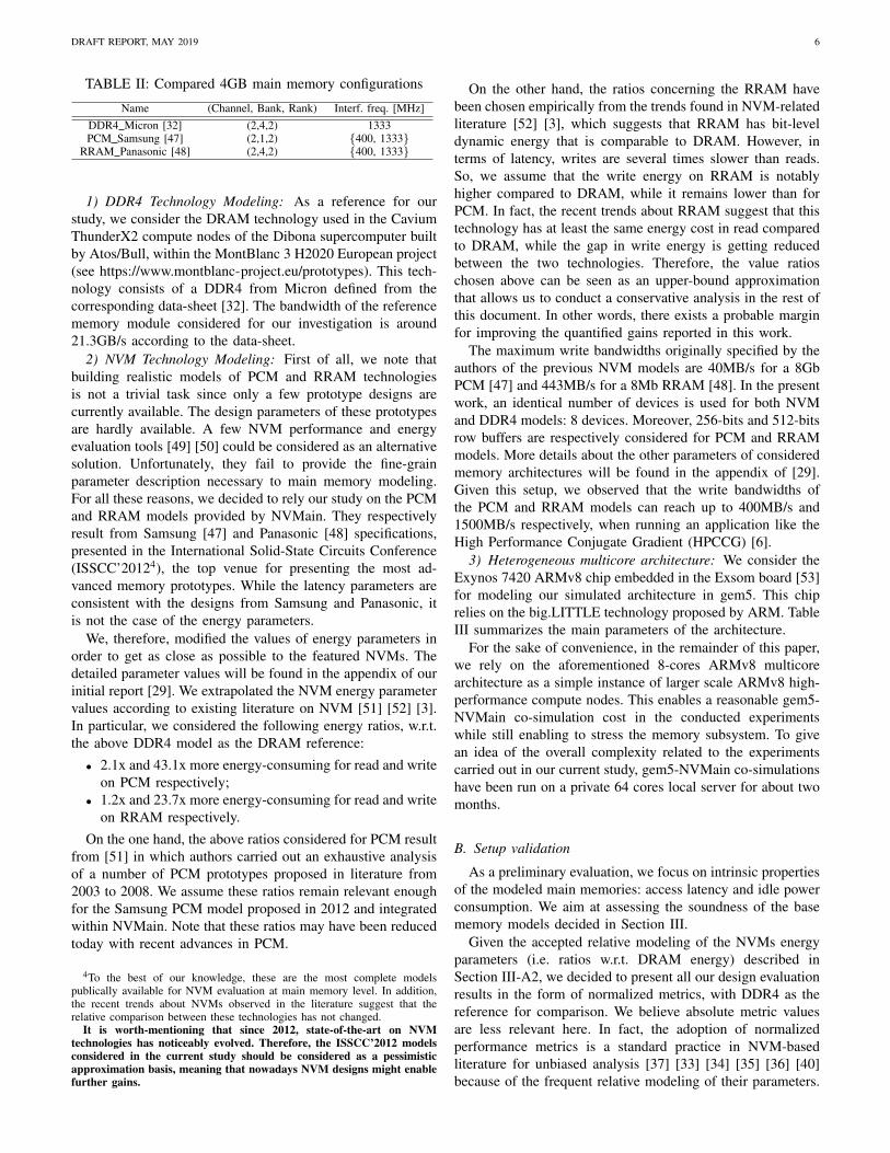
2) Idle Memory Power Consumption: An substantial ad-vantage of NVMs is that they do not require any data refreshmechanism thanks to their non-volatile nature. It is not thecase of DRAM, which can consume a non-negligible amountof energy due to refresh process and background power. Therefresh process periodically reads data from a memory areaand immediately rewrites the data to the same area, while thebackground power is due to the peripheral logic.
Given the anticipated significance of the refresh and back-ground energy consumption for DRAM, we assess its impactcompared to the considered RRAM and PCM memory models.For this purpose, we evaluate several scenarios with little-to-

DRAFT REPORT, MAY 2019 8
no access in main memory, i.e., no read, no write. In Figure4, we report the energy of a quasi-idle 4GB main memory formodified durations, varying from 1 second to 30 seconds. Thisis achieved in gem5 by executing the ”sleep” system call withdifferent input delay values in seconds. The reported valuesenable us to analyze the impact of the overhead related to thebackground power and the refresh mechanism on the DDR4memory energy consumption.
The total energy consumption computed by NVMain con-sists of the sum of four components: background energy,refresh energy, activate energy and burst energy. These param-eters are automatically produced among the output statisticsof NVMain after each simulation. This enables a fine-grainanalysis of the energy breakdown. In all experiments shownin Figure 4, we observe that with the DDR4 the energyconsumption of the main memory grows significantly withbigger input delays, due to the background and refresh energycomponents (negligible in NVMs). On the contrary, only amarginal energy increase is observed with RRAM and PCM.This shows the potential energy saving opportunity offeredby NVMs for execution scenarios where the main memoryis under-used. NVMain essentially provides two device-levelenergy models: current-mode and energy-mode [31]. Eachmode relies on a specific power estimation strategy. Thecurrent-mode uses IDD values for power calculation (as instandard DRAM simulators) and applies to DRAM systems.The energy-mode exploits energy estimations resulting fromcircuit-level simulators like NVSim [49] or CACTI [55]. Eachmemory operation increments the system energy usage, whilestandby and powerdown energies are computed from simulatedleakage values. In our experiments, the current-mode is usedfor DDR4. The energy-mode is selected for the two NVMmodels.
Fig. 5: Idle main memory energy: 4GB versus 32GB
When increasing the size of the main memory, NVMsfurther mitigate energy consumption. This is illustrated inFigure 5, where the size of the main memory is increased from4GB to 32GB while keeping unchanged the other memoryparameters. The reported results concern an execution of the”sleep” system call for 15 seconds.
The above preliminary evaluation of the NVM modelsregarding their latency and energy consumption is in linewith the existing observation from literature: refresh andbackground energy consumption has an important impact onthe global energy consumption of advanced DRAM-basedmemories [15]. This suggests the considered PCM and RRAM
models are relevant enough to be used for further investiga-tions.
In particular, provided these results, we can quantify thelatency gap between the considered NVM technologies w.r.t.a typical DDR4 model when integrated into main memory.Note that the read latencies have been determined by using abenchmark designed for this specific purpose within the streambenchmark set. It will be interesting to evaluate the impact ofNVMs application-wise.
IV. ASSESSMENT ON TYPICAL APPLICATIONS
We consider the Parsec benchmark set for evaluating theimpact of the PCM and RRAM models, compared to theMicron DDR4 model, within a 4GB main memory model.The applications provided within Parsec provide evaluationscenarios that are more representative of applications.
A. Evaluation Parsec benchmarks
1) Selected benchmarks: For the sake of simplicity, weconsider three categories of applications, each featured byone representative workload from Parsec: blackscholes, dedupand swaptions. The dedup workload is mainly memory-boundbenchmark, particularly with a high number of read transac-tions in the memory. It is dedicated to the definition of highdata stream compression ratios. The blackscholes workloadis mainly compute-intensive, with marginal memory accessescompared to the two others. It expresses an analytical pricecalculation based on the Black-Scholes partial differentialequation. Finally, the swaptions workload shows intermediatememory access properties compared to the previous two. Itapplies Monte Carlo simulation to compute prices.
These workloads are selected based on a previous charac-terization described in [56]. Their corresponding properties interms of memory access and computation load are summa-rized in Table IV. The reported values denote in billion thenumber of floating-point operations (FLOPs), read and writeinstructions.
In the rest of the document, we, therefore, consider blacksc-holes, dedup, and swaptions as the respective representativesof low memory access, high memory access, and moderatememory access applications.
TABLE IV: Breakdown of benchmark in billion instructions[56]
Benchmarks 109 FLOPs 109 Reads 109 Writesblackscholes 1.14 0.68 0.19
dedup 0 11.71 3.13swaptions 2.62 5.08 1.16
To confirm the memory access properties of the above threeworkloads with medium input sets5, we run them by consid-ering the same system setup as described in Section III-B1.The resulting profiles in terms of read and write bandwidths
5The breakdown shown in Table IV considers large input sets run on a realcomputer. At this point, it is utilized as an initial criterion for benchmarksselection w.r.t. their characteristics. In our experiments, we use rather mediuminput sets because it is more tractable with gem5 in term of simulation time.

DRAFT REPORT, MAY 2019 9
(a) blackscholes (low memory accesses)
(b) dedup (high memory access)
(c) swaptions (medium memory access)
Fig. 6: DDR4 Read/Write bandwidth for 3 benchmarks
for each of the workloads are illustrated in Figure 6. Theyare compliant with the read/write volumes characterized in[56]. Indeed the read/write bandwidth thresholds obtained withdedup and swaptions globally dominate that of blackscholessince they perform more memory accesses than blackscholes.This is distinctly visible for dedup, which has the highestmemory activity in terms of both read and write transactions,among the three benchmarks.
We notice that only a small fraction of the memory band-width is used by the three benchmarks (i.e., far from memorybandwidth saturation, which is around 21.3GB/s according tothe reference data-sheet [32]).
2) Evaluation results: Now, let us consider the executionof the three workloads by varying the memory technology in
main memory as in the previous section, i.e., DDR4, RRAM,and PCM. Medium input sets are used for the experiments.Figure 7 reports the different results. More precisely, theexecution time and the main memory energy consumption areillustrated.
On the one hand, in Figure 7a, we observe that themaximum execution slowdown between DDR4 and PCM isabout 7.2x. Between DDR4 and RRAM it is only about 1.7x.These slowdown factors of NVMs over DDR4 are obtainedwith the dedup memory-intensive workload. The high write-induced cost of NVMs, especially with PCM, exacerbatesthe slowdown compared to DDR4 as observed with dedupwhich contains more writes. Nonetheless, we can interestinglyobserve the above slowdown factors of NVMs are respectivelysmaller than the previous 11.7x and 5.5x memory latency gapobtained with the lat-mem rd benchmark (see Figure 3). Thissuggests that the detrimental impact of the intrinsic highermemory latencies of NVMs compared to DRAM, is limitedapplication-wise on corresponding execution times, even for amemory-intensive workload. For application workloads withlow and moderate memory accesses, the slowdown ratiosbetween DDR4 and NVM based scenarios are further reduced.It is the case of blackscholes and swaptions in Figure 7a.
The important overhead in execution time observed fordedup and swaptions, while using PCM in main memory, ismostly due to the write transactions. Since write latency withPCM is higher than with RRAM (see Table I), this exacerbatesthe gap between the execution times resulting in the two NVMtechnologies. The overhead in execution time observed for theswaptions workload compared to the blackscholes workloadmainly comes from the higher number of read transactionsin the former. For yet undetermined reason we observe thatfor the blackscholes workload, the PCM model unexpectedlyyields a faster execution time compared to RRAM. A possibleexplanation lies in the cache replacement policy that for thisparticular benchmark may be counter-productive, performing(unadequate) replacements faster with DDR4 and RRAM thatin turn result in higher cache miss rate.
On the other hand, the energy consumption of the mainmemory with NVMs is always smaller than with DDR4, nomatter the workload type (see Figure 7b). Of course, theenergy gap observed application-wise is more important thanwith the ”Idle Memory” scenario described formerly in Figure4, due to the dynamic activity of the memory. To appreciatethe global benefit of NVM integration in main memory, letus consider the Energy-Delay-Product (EDP) from the mainmemory perspective only. The EDP is calculated as the productof the workload execution time and the energy consumed bythe main memory during the execution time. The aim is toassess the global benefit of each design alternative. Figure7c shows the normalized EDP of all memory configurations,according to the three representative workloads. One can seethat NVMs always provide better EDP than DDR4, except forone scenario: when dedup is executed while the main memoryis in PCM. In other words, for memory-intensive applications,the energy reduction enabled by the PCM technology cannotbe compensated by its higher device-level read/write latencies.

DRAFT REPORT, MAY 2019 10
(a) Normalized system executime time (b) Normalized memory energy consumption (c) Normalized memory EDP
Fig. 7: System execution time, energy consumption and Energy-Delay-Product of main memory with DDR4 and RRAM andPCM (smaller execution time, energy consumption and EDP are better)
B. Evaluation on Typical HPC workloads
1) Memory-bound benchmarks: We further evaluate NVMintegration in main memory by considering the so-calledMontBlanc benchmarks [57], which are representative of HPCworkloads. We select four memory-bound benchmarks thatfeature various memory accesses and computational require-ments. The 3D Stencil (3dstc) benchmark, which takes asinput a 3D volume and produces an output 3D volume of theidentical size. It is a memory-bound benchmark that featuresstridden memory accesses. The N-Body (nbody) benchmarkrequires a number of input parameters including a number ofbodies including their position, mass, and initial velocity. Next,it updates these parameters based on gravitational interferencebetween bodies. It features irregular memory accesses. TheSparse Vector-Matrix Multiplication (spvm) computes a vectorresulting from the product of its input vector and sparsematrix. It features computational behaviors with potentialload imbalance. Finally, Vector Operation (vecop) computesa vector resulting from an element-wise addition of two inputvectors. It captures intensive regular computational behaviors.Note that vector-matrix multiplication and vector addition arememory-bound algorithms [58].
(a) Normalized system exectution time
(b) Normalized memory energy consumption
Fig. 8: Normalized exec. time and main memory energy ofselected Montblanc benchmarks [57]
The execution time and memory energy consumption ob-tained when executing the above HPC benchmarks are shownin Figure 8. Here, an interesting insight concerns the mainmemory energy consumption. Unlike with dedup which hasmany memory accesses, NVMs lead to worse global memoryenergy consumption with the 3dstc and vecop benchmarks.However, for the n-body and spvm benchmarks, NVMs andespecially RRAM, significantly improve memory energy con-sumption, so that the corresponding EDP remains better thanthat obtained with DDR4.
The above results motivate the need of design solutions suchas hybrid DRAM-NVM main memory designs (see SectionII). Such designs are capable of adjusting the choice of thesuitable memory target according to the energy outcome ofgiven memory-bound workloads. This will enable to mitigatethe energy penalty.
2) Representative mini-applications: Now, we evaluatethe impact of designed system models on two HPC mini-applications that can be simulated in a reasonable time.
The Livermore Unstructured Lagrangian Explicit Shock Hy-drodynamics (Lulesh) mini-application [59] encodes a discreteapproximation of the hydrodynamics equations. It partitionsthe spatial problem domain into a collection of volumetricelements defined by a mesh. It presents high instruction-level and memory-level parallelism with bursts of independentmemory accesses. We consider its implementation in OpenMP.
The High-Performance Conjugate Gradient (HPCG) mini-application [6] for a 3D chimney domain on an arbitrarynumber of processors. It has been devised with the aim ofproviding a metric for assessing HPC systems. It enables toexercise computational and data access patterns, which featurea range of applications. HPCG shares a similar goal as thepopular High-Performance LINPACK (HPL) benchmark [60].The HPCCG 1.0 OpenMP implementation is considered in theevaluation presented below. It includes three main computationkernels called waxpby (sum of two scaled vectors), ddot (dotproduct of two vectors) and sparsemv (sparse matrix vectorproduct). Its three input parameters nx, ny and nz denote thenumber of nodes in the 3D dimensional domain. Here, it willbe executed on 8-cores big.LITTLE architecture.
Analysis of execution outputs. The output correspondingto 8-threads execution of Lulesh with the previous threemain memory configurations (DDR4, RRAM, and PCM) is

DRAFT REPORT, MAY 2019 11
summarized in Table V. The main performance measurementsreported by the Lulesh application are summarized. Elapsedtime denotes how much time it takes to perform the simulation.Grind time denotes the time it takes to update a single zonefor one iteration of the time-step loop. Lower values ofthis measure mean better performance. The Lulesh Figure-Of-Merit (FOM) provides the number of updated zones persecond. These results are obtained by considering as inputs:a problem size of 153 per domain until completion, while thetotal number of elements is 3375.
TABLE V: Lulesh execution statistics w.r.t. selected memorytechnologies
DDR4 RRAM PCMElapsed time (s) 2.54 2.51 6.04
Grind time (µs / z / c) 1.88 1.86 A.47FOM (z / s) 531.08 536.82 223.45
The performance numbers obtained upon executing HPCCGwith three main memory configurations are summarized in Ta-ble VI. As expected, the configuration with DDR4 provides thebest performance in terms of mega floating point operationsper second (MFLOPS). The performance degradation inducedby RRAM is very limited compared to PCM. This is due totheir respective high memory access latencies. These results,obtained after 149 iterations, correspond to a parallel executionof 8 OpenMP threads, where the input parameters (nx, ny, nz)equal (104, 104, 104).
TABLE VI: HPCCG execution statistics w.r.t. selected mem-ory technologies
DDR4 RRAM PCM
Time (s)
DDOT 3.67 4.72 14.08WAXPBY 14.94 11.48 70.34SPARSEMV 41.27 59.78 218.28Total 59.95 76.04 302.82
Performance(MFLOPS)
DDOT 182.37 141.79 47.60WAXPBY 67.31 87.56 14.29SPARSEMV 219.27 151.39 41.46Total 178.91 141.05 35.42
From these results, the DDR4 and RRAM configurationslead to almost similar performance results with respectively531.08 and 536.82 z/s FOM values (RRAM even slightlyoutperforms DDR4). They are far better than with the PCMconfiguration, which has penalizing memory access latency.
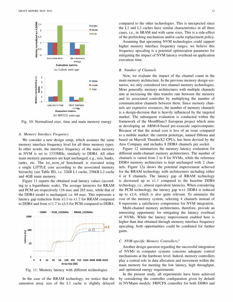
Analysis of memory activity. We focus on the mainmemory activity for the previous two mini-applications inorder to analyze the implication of the different memorytechnologies w.r.t. the performance results described above.Figure 9 presents the main memory read/write bandwidths forthe various technologies.
Overall, the Lulesh mini-application exhibits lower band-width thresholds (both for read and write) than HPCCG.Therefore, the performance penalty is expected to be morevisible with the latter. This explains why the gap in executiontimes between DDR4 configuration and NVM configurationsis more important for HPCCG, e.g., more than four timeswhen comparing DDR4 and PCM (see Figure 10b). This gap
(a) Lulesh mini-app
(b) HPCCG mini-app
Fig. 9: Main memory Read/Write bandwidth for DDR4
remains below 2.5x for these technologies when consideringLulesh (see Figure 10a). Note that for both mini-applications,the RRAM technology provides comparable execution timethan DDR4.
The main memory energy consumption shown in Figure 10for both mini-applications shows that NVMs always provideimprovements compared DDR4, despite their possible perfor-mance penalty. Nevertheless, when considering the Energy-Delay-Product (EDP) figure-of-merit, PCM never appears asefficient as DDR4 because of the high performance degrada-tion it induces. This is not the case of RRAM, which providesa better EDP than the DDR4 configuration, whatever the mini-application.
V. ANALYSIS OF A FEW MEMORY DESIGN CHOICES
The results presented in Section IV show that NVMs canimprove the energy-efficiency for typical high-performanceworkloads. Now, we explore a few design parameters thatmight have an influence on the efficient integration of NVMsin the SoC reference design introduced in Figure 1. In Sec-tion III-B, our previous experiments, we evaluated the readlatency of main memory by configuring the memory interfacefrequency of DDR4 to 1333MHz, while the memory interfacefrequencies of both PCM and RRAM is set to 400MHz (seeSection III-B1). An interesting direction is to explore thepossibility of upscaling the memory interface frequency ofNVMs so as to reduce their latency gap as observed previously.Another direction concerns the number of memory channels(see Figure 2).
DRAFT REPORT, MAY 2019 12
(a) Lulesh mini-app
(b) HPCCG mini-app
Fig. 10: Normalized exec. time and main memory energy
A. Memory Interface Frequency
We consider a new design setup, which assumes the samememory interface frequency level for all three memory types.In other words, the interface frequency of the main memoryin NVM is set to 1333MHz, similarly to DDR4. All othermain memory parameters are kept unchanged, e.g., size, banks,ranks, etc. The lat mem rd benchmark is executed usinga single LITTLE core according to the associated memoryhierarchy (see Table III), i.e. 32kB L1 cache, 256kB L2 cacheand 4GB main memory.
Figure 11 reports the obtained read latency values (accord-ing to a logarithmic scale). The average latencies for RRAMand PCM are respectively 116 nsec and 265 nsec, while that ofthe DDR4 model is unchanged, i.e. 69 nsec. This represents alatency gap reduction from x5.5 to x1.7 for RRAM comparedto DDR4 and from x11.7 to x3.8 for PCM compared to DDR4.
Fig. 11: Memory latency with different technologies
In the case of the RRAM technology, we notice that thesaturation array size of the L1 cache is slightly delayed
compared to the other technologies. This is unexpected sincethe L1 and L2 caches have similar characteristics in all threecases, i.e., in SRAM and with same sizes. This is a side-effectof the prefetching mechanism and/or cache replacement policy.
Assuming that upcoming NVM technologies could supporthigher memory interface frequency ranges, we believe thisfrequency upscaling is a potential optimization parameter formitigating the impact of NVM latency overhead on applicationexecution time.
B. Number of Channels
Now, we evaluate the impact of the channel count in themain memory architecture. In the previous memory design sce-narios, we only considered two channel memory technologies.More generally, memory architectures with multiple channelsaim at increasing the data transfer rate between the memoryand its associated controller by multiplying the number ofcommunication channels between them. Since memory chan-nels are expensive resources, the number of memory channelsis a design-decision that is heavily influenced by the targetedmarket. The subsequent evaluation is conducted within theframework of the MontBlanc3 European project which aimsat developing an ARMv8-based pre-exascale supercomputer.Because of that the actual cost is less of an issue comparedto a mobile market: the current prototype, named Dibona andbased on Marvell ThunderX2 CPUs, has been devised by theAtos Company and includes 8 DDR4 channels per socket.
Figure 12 summarizes the memory latency evaluation fordifferent multi-channel memory architectures. The number ofchannels is varied from 2 to 8 for NVMs, while the referenceDDR4 memory architecture is kept unchanged with 2 chan-nels. Figure 12a shows the potential improvement achievedfor the RRAM technology with architectures including either4 or 8 channels. The latency gap of RRAM technologyis decreased up to x1.1 compared to the baseline DDR4technology, i.e., almost equivalent latencies. When consideringthe PCM technology, the latency gap w.r.t. DDR4 is reducedup to x2.6, which is also quite relevant. To minimize thecost of the memory system, selecting 4 channels instead of8 represents a satisfactory compromise for NVM integration.
Multi-channel memory architectures, therefore, provide aninteresting opportunity for mitigating the latency overheadof NVMs. While the latency improvement enabled here ishigher than that obtained through memory interface frequencyupscaling, both opportunities could be combined for furthergains.
C. NVM-specific Memory Controllers?
Another design question regarding the successful integrationof NVMs in computer systems concerns adequate controlmechanisms at the hardware level. Indeed, memory controllersplay a central role in data allocation and movement within themain memory for meeting the low latency, high throughput,and optimized energy requirements.
In the present study, all experiments have been achievedby considering the controller configuration given by defaultin NVMaim models: FRFCFS controller for both DDR4 and

DRAFT REPORT, MAY 2019 13
(a) RRAM configurations
(b) PCM configurations
Fig. 12: Comparison of NVM memory system latencies with2, 4 and 8 channels versus the reference DDR4 configuration(zoom from L2 cache to main memory)
RRAM, and FRFCFS-WQF controller for PCM. This leavesroom for further design optimizations since the memory ac-cesses have variable costs depending on the selected controller.Typically, the average main memory latency of PCM can bereduced by 16% by selecting the FRFCFS controller instead ofFRFCFS-WQF. Furthermore, the row buffer design inside thecontroller could take into account the different latencies of hitsand misses depending on the memory technology: DRAM andPCM are known to have similar row buffer hit latency, whilethe row buffer miss latency is larger for PCM due to theirrelated higher array access latency [11].
The aforementioned controller design should exploit the het-erogeneous/homogeneous nature of the main memory. Someexisting work already addressed the case of hybrid DRAM-NVM main memory design, where row buffer locality-awaredata placement policies are proposed [61]. For instance, the au-thors observed that streaming data accesses are PCM-friendly,while other data accesses (with reuse) are rather DRAM-friendly for data placement. In the case of main memoryintegrating only NVM, as evaluated in the present work, thedesign of the memory controller is an open question thatremains to be addressed. We believe that revisiting the designprinciple of such a mechanism can improve the benefits ofNVM integration by taking their specificity into account.
VI. GAINED INSIGHTS FOR SOC INTEGRATION
From all the previous experimental results, we draw moreconcretely the envisioned most favorable NVM integration inthe memory hierarchy beyond cache levels. We briefly addressthe programmability issue of compute nodes in presence ofNVMs in main memory.
A. General observations
Our experiments show that NVM can relevantly improve themain memory energy consumption, at the expense of limitedpenalty on performance. The announced cost-effectiveness6 ofthese emerging memory technologies compared to concurrenttechnologies, such as DRAM and NAND Flash, makes thisperspective credible. Given a relative cost per bit of 1 forDRAM, it is around 0.25 for PCM and RRAM [37].
The perspective of their integration in future SoCs is par-ticularly promising with the RRAM technology, while PCMmay incur non-negligible performance degradation. The PCMtechnology rather appears as an in-between good candidatew.r.t. faster main memories and slower storage-class memories(this observation additionally holds for the recent 3D XPointtechnology from Intel and Micron [26]. It is worth-mentioningthat NVMain only enables to model and evaluate main mem-ory level technology integration. Dealing with storage levelintegration would require new simulation tools. Figure 13summarizes this idea.
Fig. 13: Memory technologies within memory hierarchy.
Note that our study does not consider alternative NVMintegration approaches, such as hybrid memory design asaddressed widely in existing literature [11]. These approachesare a complementary solution that may have an impact on theway NVM integration is seen through the memory hierarchydepicted in Figure 13.
Actually, the joint emergence of HBM and NVM technolo-gies will likely lead to revisit the junction between memoryhierarchy and storage as we know it in today’s systems.Indeed, why would designers keep on considering the DRAMtechnology for main memory, while NVM could provide allthe necessary memory capacity? On the other hand, why wouldindustry keep on deploying chips with hard drive supportswhile NVM controllers could help to fill this demand? Remov-ing all unnecessary design features has been always the pointfor the design of optimized ARM-based HPC SoCs to savepower and increase the system energy-efficiency. Therefore,for high-end server capability such as in HPC domain, a new
6https://www.computerworld.com/article/3194147/data-storage/faq-3d-xpoint-memory-nand-flash-killer-or-dram-replacement.html

DRAFT REPORT, MAY 2019 14
memory design trade-off is definitely to be found betweenDRAM, NVMs and SATA connection in the near future.
B. Impact on programming models
Beyond the above architectural design considerations, theintegration of NVMs in multicore SoCs calls for reconsideringthe entire system design stack. This concerns in particular theimpact on programming models and system software. In orderto anticipate this issue, we evaluate two parallel programmingmodels through different versions of the same applicationwhile having NVMs in main memory. These programmingmodels are supposed to involve different memory activitiesaccording to their associated runtime management systems.
We consider the OpenMP version 2.3 and OmpSs program-ming models. OpenMP7 is a popular shared-memory parallelprogramming interface. The OpenMP version 2.3 (in whichour benchmarks and mini-applications are implemented) fea-tures a thread-based fork-join task allocation model as illus-trated in Figure 14a. It consists of a set of compiler directives,library routines and environment variables for the developmentof parallel applications. OmpSs [62] is a task-based program-ming model (see Figure 14b) that improves OpenMP withsupport for irregular and asynchronous parallelism, and forheterogeneous architectures. It incorporates dataflow conceptsenabling its compiler/runtime to automatically move datawhenever necessary and to apply various useful optimizations.
(a) OpenMP (b) OmpSs
Fig. 14: OpenMP fork-join region vs OmpSs task graph
The Nanos++ runtime used with OmpSs enables anasymmetry-conscious task scheduling [63]. It incorporatesCriticality-Aware Task Scheduler (CATS) scheduling policyCATS, which exploits the criticality of generated tasks toschedule them during execution. The most critical tasks, i.e.,those appearing on the critical execution path, are executed bythe high-frequency cores. Typically, such tasks are representedin red color in Figure 14b. Less critical tasks are executed onlow-power cores. These tasks are denoted by green color inFigure 14b.
To compare both programming models, we consider twocorresponding versions of the HPCCG mini-application. Weobserve that the OmpSs version of HPCCG provides betterperformance than the OpenMP version. This is mainly dueto the CATS scheduler of the former. On the other hand, theread/write bandwidth obtained with OmpSs version, shown
7https://www.openmp.org
in Figure 15, is significantly higher than that of OpenMPversion (see Figure 9). For instance, the read bandwidth isimproved by about 4x, 3x and 1.8x for DDR4, RRAM, andPCM respectively. However, the write bandwidth is improvedmerely marginally.
Fig. 15: Main memory bandwidth for OmpSs version ofHPCCG with DDR4.
The impact of this improvement is illustrated in Figure 16.The execution time and main memory energy consumption arecompared separately for each memory technology, accordingto the two programming models for HPCCG. The OmpSs run-time enables to reduce by more than 50% the execution time ofthe OpenMP version for all three memory technologies. Thisis in-line with our previous observations when comparing bothprogramming models [64]. It additionally allows a reduction ofenergy consumption, by 60% for DDR4 and by 20% for PCM.However, it marginally increases the energy consumption forRRAM (around 2%). This is due to the notable increase inwrite bandwidth enabled by OmpSs scheduler, specifically forRRAM. Writes on NVMs are very expensive operations bothin latency and energy consumption.
VII. CONCLUDING REMARKS
In this paper, we evaluated two relevant emerging NVMtechnologies at the main memory level, to analyze their impacton both system performance and main memory energy. Keymotivation is to quantify as much as possible the impact ofNVMs in explored design scenarios. Starting from the PCMand RRAM model templates provided by the NVMain simula-tion framework, we enhanced them through some extrapolationrelying on existing literature. The NVM integration has beenevaluated with the gem5 cycle-approximate simulator whileconsidering a heterogeneous ARMv8 multicore system model(such systems are envisioned as good candidates for computenode design in HPC domain [2]). A subset of representativeParsec benchmarks and two typical mini-applications fromHPC domain have been used as evaluation workloads.
Our experiments showed RRAM represents a very goodcandidate for energy issue mitigation at the main memorylevel, while PCM would be a better candidate for storagelevel. RRAM is competitive enough compared to DDR4 fromthe viewpoint of system-level performance. Most importantly,

DRAFT REPORT, MAY 2019 15
(a) Normalized execution time
(b) Normalized energy consumption
Fig. 16: Separate comparison per memory technology forHPCCG mini-application: OpenMP vs OmpSs
it enables a reduction of main memory energy consumptionby up to 50%. While PCM does not offer such benefits atthe main memory level, it could be a more suitable candidatefor storage level. Currently, at storage level solutions for theserver market are mostly implementing SSD drives: throughCPU SATA features or through PCIe devices for NVMe disks.PCM appears a viable alternative for high-performance storageas well as for high-performance computing. Nonetheless, tosustain this gain expected from emerging NVMs, complemen-tary mechanisms (e.g., targeting wear-leveling) or technologyimprovements regarding write endurance will be helpful. Somecandidate solutions already exist [23].
It is worth-mentioning that the experiments conducted inthis study rely on NVM models published in 2012 by Samsungand Panasonic. This decision was motivated by the high-levelof confidence on these published results. These rather oldmodels can be seen as conservative approximations of thesetechnologies and their potential: the state-of-the-art on NVMtechnologies has notably improved over the last years andthe gains observed in this study might get better as NVMtechnologies progress.
ACKNOWLEDGMENT
This work was supported in part by the Mont-Blanc3 H2020project under the grant number 671697, and the CONTIN-UUM French ANR project under the grant number ANR-15-CE25-0007-01.
REFERENCES
[1] K. Bergman, S. Borkar, D. Campbell, W. Carlson, W. Dally, M. Den-neau, P. Franzon, W. Harrod, J. Hiller, S. Karp, S. Keckler, D. Klein,R. Lucas, M. Richards, A. Scarpelli, S. Scott, A. Snavely, T. Sterling,
R. S. Williams, K. Yelick, K. Bergman, S. Borkar, D. Campbell, W. Carl-son, W. Dally, M. Denneau, P. Franzon, W. Harrod, J. Hiller, S. Keckler,D. Klein, P. Kogge, R. S. Williams, and K. Yelick, “ExaScale ComputingStudy: Technology Challenges in Achieving Exascale Systems PeterKogge, Editor & Study Lead,” 2008.
[2] J. Wanza Weloli, S. Bilavarn, M. De Vries, S. Derradji, and C. Belleudy,“Efficiency modeling and exploration of 64-bit arm compute nodes forexascale,” Microprocess. Microsyst., vol. 53, no. C, pp. 68–80, Aug.2017. [Online]. Available: https://doi.org/10.1016/j.micpro.2017.06.019
[3] J. Boukhobza, S. Rubini, R. Chen, and Z. Shao, “Emerging nvm:A survey on architectural integration and research challenges,” ACMTrans. Des. Autom. Electron. Syst., vol. 23, no. 2, pp. 14:1–14:32, Nov.2017. [Online]. Available: http://doi.acm.org/10.1145/3131848
[4] J. Russell, “Cavium Announces GA for ThunderX2;Touts OEM Support,” https://www.hpcwire.com/2018/05/07/cavium-announces-ga-for-thunderx2-touts-oem-support/, [Accessed:May 7, 2018].
[5] S. M. Tam, H. Muljono, M. Huang, S. Iyer, K. Royneogi, N. Satti,R. Qureshi, W. Chen, T. Wang, H. Hsieh et al., “Skylake-sp: A 14nm28-core xeon R© processor,” in Solid-State Circuits Conference-(ISSCC),2018 IEEE International. IEEE, 2018, pp. 34–36.
[6] J. Dongarra, M. A. Heroux, and P. Luszczek, “High-performanceconjugate-gradient benchmark,” Int. J. High Perform. Comput.Appl., vol. 30, no. 1, pp. 3–10, Feb. 2016. [Online]. Available:https://doi.org/10.1177/1094342015593158
[7] S. McIntosh-Smith, J. Price, T. Deakin, and A. Poenaru, “Comparativebenchmarking of the first generation of hpc-optimised arm processorson isambard,” in Cray User Group, 5 2018.
[8] T. Yoshida, M. Hondou, T. Tabata, R. Kan, N. Kiyota, H. Kojima,K. Hosoe, and H. Okano, “Sparc64 xifx: Fujitsu’s next-generationprocessor for high-performance computing,” Micro, IEEE, vol. 35, pp.6–14, 03 2015.
[9] M. Feldman, “Fujitsu Reveals Details of Processor That WillPower Post-K Supercomputer,” https://www.top500.org/news/fujitsu-reveals-details-of-processor-that-will-power-post-k-supercomputer/,[Accessed: August 22, 2018].
[10] HUAWEI, “Huawei Unveils Industry’s Highest-Performance ARM-based CPU,” https://www.huawei.com/en/press-events/news/2019/1/huawei-unveils-highest-performance-arm-based-cpu, [Accessed: Jan07, 2019].
[11] O. Mutlu, “Opportunities and challenges of emerging memory technolo-gies,” 2017, invited Talk during ARM Research Summit.
[12] K. Lim, J. Chang, T. Mudge, P. Ranganathan, S. K. Reinhardt, andT. F. Wenisch, “Disaggregated memory for expansion and sharing inblade servers,” SIGARCH Comput. Archit. News, vol. 37, no. 3, pp.267–278, Jun. 2009. [Online]. Available: http://doi.acm.org/10.1145/1555815.1555789
[13] O. Mutlu and L. Subramanian, “Research problems and opportunitiesin memory systems,” Supercomput. Front. Innov.: Int. J., vol. 1, no. 3,pp. 19–55, Oct. 2014. [Online]. Available: http://dx.doi.org/10.14529/jsfi140302
[14] C. Lefurgy, K. Rajamani, F. Rawson, W. Felter, M. Kistler,and T. W. Keller, “Energy management for commercial servers,”Computer, vol. 36, no. 12, pp. 39–48, Dec. 2003. [Online]. Available:https://doi.org/10.1109/MC.2003.1250880
[15] I. Bhati, M.-T. Chang, Z. Chishti, S.-L. Lu, and B. Jacob, “Dramrefresh mechanisms, penalties, and trade-offs,” IEEE Trans. Comput.,vol. 65, no. 1, pp. 108–121, Jan. 2016. [Online]. Available:http://dx.doi.org/10.1109/TC.2015.2417540
[16] S. Bhatti, R. Sbiaa, A. Hirohata, H. Ohno, S. Fukami, andS. Piramanayagam, “Spintronics based random access memory:a review,” Materials Today, vol. 20, no. 9, pp. 530 – 548,2017. [Online]. Available: http://www.sciencedirect.com/science/article/pii/S1369702117304285
[17] S. Senni, L. Torres, G. Sassatelli, A. Gamatie, and B. Mussard, “Ex-ploring mram technologies for energy efficient systems-on-chip,” IEEEJournal on Emerging and Selected Topics in Circuits and Systems, vol. 6,no. 3, pp. 279–292, Sep. 2016.
[18] S. Senni, T. Delobelle, O. Coi, P. Peneau, L. Torres, A. Gamatie,P. Benoit, and G. Sassatelli, “Embedded systems to high performancecomputing using stt-mram,” in Design, Automation Test in EuropeConference Exhibition (DATE), 2017, March 2017, pp. 536–541.
[19] R. Bouziane, E. Rohou, and A. Gamatie, “Compile-time silent-storeelimination for energy efficiency: an analytic evaluation for non-volatilecache memory,” in Proceedings of the RAPIDO 2018 Workshop onRapid Simulation and Performance Evaluation: Methods and Tools,

DRAFT REPORT, MAY 2019 16
Manchester, UK, January 22-24, 2018., D. Chillet, Ed. ACM, 2018, pp.5:1–5:8. [Online]. Available: https://doi.org/10.1145/3180665.3180666
[20] F. M. Q. Pereira, G. V. Leobas, and A. Gamatie, “Static prediction ofsilent stores,” TACO, vol. 15, no. 4, pp. 44:1–44:26, 2019. [Online].Available: https://dl.acm.org/citation.cfm?id=3280848
[21] P. Peneau, D. Novo, F. Bruguier, L. Torres, G. Sassatelli, andA. Gamatie, “Improving the performance of STT-MRAM LLC throughenhanced cache replacement policy,” in Architecture of ComputingSystems - ARCS 2018 - 31st International Conference, Braunschweig,Germany, April 9-12, 2018, Proceedings, ser. Lecture Notes inComputer Science, M. Berekovic, R. Buchty, H. Hamann, D. Koch, andT. Pionteck, Eds., vol. 10793. Springer, 2018, pp. 168–180. [Online].Available: https://doi.org/10.1007/978-3-319-77610-1\ 13
[22] R. Bouziane, E. Rohou, and A. Gamatie, “Energy-efficient memorymappings based on partial wcet analysis and multi-retention timestt-ram,” in Proceedings of the 26th International Conferenceon Real-Time Networks and Systems, ser. RTNS ’18. NewYork, NY, USA: ACM, 2018, pp. 148–158. [Online]. Available:http://doi.acm.org/10.1145/3273905.3273908
[23] A. A. Garcıa, R. de Jong, W. Wang, and S. Diestelhorst, “Composinglifetime enhancing techniques for non-volatile main memories,” inProceedings of the International Symposium on Memory Systems, ser.MEMSYS ’17. New York, NY, USA: ACM, 2017, pp. 363–373.[Online]. Available: http://doi.acm.org/10.1145/3132402.3132411
[24] R. Neale, D. Nelson, and G. E. Moore, “Nonvolatile and repro-grammable, the read-mostly memory is here,” Electronics, vol. 43,no. 20, pp. 56–60, 1970.
[25] M. Stanisavljevic, H. Pozidis, A. Athmanathan, N. Papandreou, T. Mit-telholzer, and E. Eleftheriou, “Demonstration of reliable triple-level-cell (TLC) phase-change memory,” in Proceedings of the InternationalMemory Workshop (IMW), 2016, pp. 1–4.
[26] Intel, “Intel and Micron Produce Breakthrough MemoryTechnology,” https://newsroom.intel.com/news-releases/intel-and-micron-produce-breakthrough-memory-technology/,[Accessed: February-2017].
[27] H. Akinaga and H. Shima, “Resistive random access memory (reram)based on metal oxides,” Proceedings of the IEEE, vol. 98, no. 12, pp.2237–2251, 2010.
[28] E. Herald, “UMC is a foundry partner for Panasonic in making ResistiveRAM,” http://www.eeherald.com/section/news/owns20170202003.html,[Accessed: February-2017].
[29] A. Gamatie, A. Nocua, G. Sassatelli, D. Novo, M. Robert, andL. Torres, “D3.7 - Final Report on Memory Hierarchy Investigations.”https://www.montblanc-project.eu/wp-content/uploads/2019/02/MB3 D3.7-Final-Report-on-Memory-Hierarchy-Investigation-1.pdf,MontBlanc 3 project, Tech. Rep., 2018.
[30] gem5, “The gem5 simulator,” http://www.gem5.org, 2016, [Accessed:February-2017].
[31] M. Poremba, T. Zhang, and Y. Xie, “Nvmain 2.0: A user-friendlymemory simulator to model (non-)volatile memory systems,” ComputerArchitecture Letters, vol. 14, no. 2, pp. 140–143, 2015. [Online].Available: http://dx.doi.org/10.1109/LCA.2015.2402435
[32] Micron, “DDR4 SDRAM RDIMM - MTA18ASF2G72PDZ - 16GB,”https://www.google.com/url?sa=t&rct=j&q=&esrc=s&source=web&cd=1&ved=0ahUKEwif55DcxtDbAhUKVxQKHbsiBaAQFggoMAA&url=https%3A%2F%2Fwww.micron.com%2F∼%2Fmedia%2Fdocuments%2Fproducts%2Fdata-sheet%2Fmodules%2Frdimm%2Fddr4%2Fasf18c2gx72pdz.pdf&usg=AOvVaw1YvGKpxb5Aok0KYGnbhwrE,2015, online; accessed in June 2018.
[33] B. C. Lee, P. Zhou, J. Yang, Y. Zhang, B. Zhao, E. Ipek, O. Mutlu, andD. Burger, “Phase-change technology and the future of main memory,”IEEE micro, vol. 30, no. 1, 2010.
[34] J. Meza, J. Li, and O. Mutlu, “A case for small row buffers in non-volatile main memories,” in Proceedings of the International Conferenceon Computer Design (ICCD), 2012, pp. 484–485.
[35] E. Kultursay, M. Kandemir, A. Sivasubramaniam, and O. Mutlu, “Eval-uating stt-ram as an energy-efficient main memory alternative,” inProceedings of the International Symposium on Performance Analysisof Systems and Software (ISPASS). IEEE, 2013, pp. 256–267.
[36] H. Yoon, J. Meza, R. Ausavarungnirun, R. A. Harding, and O. Mutlu,“Row buffer locality aware caching policies for hybrid memories,”in Proceedings of the International Conference on Computer Design(ICCD), 2012, pp. 337–344.
[37] F. Ware, J. Bueno, L. Gopalakrishnan, B. Haukness, C. Haywood,T. Juan, E. Linstadt, S. A. McKee, S. C. Woo, K. L. Wright,C. Hampel, and G. Bronner, “Architecting a hardware-managedhybrid dimm optimized for cost/performance,” in Proceedings of the
International Symposium on Memory Systems, ser. MEMSYS ’18.New York, NY, USA: ACM, 2018, pp. 327–340. [Online]. Available:http://doi.acm.org/10.1145/3240302.3240303
[38] G. H. Loh and M. D. Hill, “Efficiently enabling conventional blocksizes for very large die-stacked dram caches,” in Proceedings of theInternational Symposium on Microarchitecture, 2011, pp. 454–464.
[39] J. Meza, J. Chang, H. Yoon, O. Mutlu, and P. Ranganathan, “Enablingefficient and scalable hybrid memories using fine-granularity dram cachemanagement,” IEEE Computer Architecture Letters, vol. 11, no. 2, pp.61–64, 2012.
[40] J. Meza, Y. Luo, S. Khan, J. Zhao, Y. Xie, and O. Mutlu, “A casefor efficient hardware/software cooperative management of storage andmemory,” in Proceedings of the Workshop on Energy-Efficient Design,2013, pp. 1–7.
[41] J. Zhao, O. Mutlu, and Y. Xie, “Firm: Fair and high-performancememory control for persistent memory systems,” in Proceedings of theInternational Symposium on Microarchitecture, 2014, pp. 153–165.
[42] A. Butko, A. Gamatie, G. Sassatelli, L. Torres, and M. Robert, “Designexploration for next generation high-performance manycore on-chipsystems: Application to big.little architectures,” in 2015 IEEE ComputerSociety Annual Symposium on VLSI, July 2015, pp. 551–556.
[43] A. Butko, F. Bruguier, A. Gamatie, G. Sassatelli, D. Novo, L. Torres, andM. Robert, “Full-system simulation of big.little multicore architecturefor performance and energy exploration,” in MCSoC. IEEE ComputerSociety, 2016, pp. 201–208.
[44] P. Rosenfeld, E. Cooper-Balis, and B. Jacob, “Dramsim2: A cycle ac-curate memory system simulator,” IEEE Computer Architecture Letters,vol. 10, no. 1, pp. 16–19, Jan 2011.
[45] M. Jung, C. Weis, and N. Wehn, “Dramsys: A flexible dram subsystemdesign space exploration framework,” IPSJ Transactions on System LSIDesign Methodology, vol. 8, pp. 63–74, 2015.
[46] Y. Kim, W. Yang, and O. Mutlu, “Ramulator: A fast and extensibledram simulator,” IEEE Computer Architecture Letters, vol. 15, no. 1,pp. 45–49, Jan 2016.
[47] Y. Choi, I. Song, M.-H. Park, H. Chung, S. Chang, B. Cho, J. Kim,Y. Oh, D. Kwon, J. Sunwoo et al., “A 20 nm 1.8 V 8 Gb PRAM with40 MB/s program bandwidth,” in Proceedings of the International Solid-State Circuits Conference, 2012, pp. 46–48.
[48] A. Kawahara, R. Azuma, Y. Ikeda, K. Kawai, Y. Katoh, K. Tanabe,T. Nakamura, Y. Sumimoto, N. Yamada, N. Nakai et al., “An 8 Mb multi-layered cross-point ReRAM macro with 443 MB/s write throughput,” inProceedings of the International Solid-State Circuits Conference, 2012,pp. 432–434.
[49] X. Dong, C. Xu, Y. Xie, and N. P. Jouppi, “Nvsim: A circuit-levelperformance, energy, and area model for emerging nonvolatile mem-ory,” Computer-Aided Design of Integrated Circuits and Systems, IEEETransactions on, vol. 31, no. 7, pp. 994–1007, 2012.
[50] S. Mittal, R. Wang, and J. Vetter, “Destiny: A comprehensive toolwith 3d and multi-level cell memory modeling capability,” Journal ofLow Power Electronics and Applications, vol. 7, no. 3, 2017. [Online].Available: http://www.mdpi.com/2079-9268/7/3/23
[51] B. C. Lee, E. Ipek, O. Mutlu, and D. Burger, “Architecting phasechange memory as a scalable dram alternative,” SIGARCH Comput.Archit. News, vol. 37, no. 3, pp. 2–13, Jun. 2009. [Online]. Available:http://doi.acm.org/10.1145/1555815.1555758
[52] M. H. Kryder and C. soo Kim, “After hard driveswhat comes next?”IEEE Transactions on Magnetics, vol. 45, pp. 3406–3413, 2009.
[53] HowChip, “Exsom board,” 2016, http://howchip.com/ExSOM7420SB.php.
[54] L. W. McVoy, C. Staelin et al., “lmbench: Portable Tools for Perfor-mance Analysis,” in USENIX annual technical conference. San Diego,CA, USA, 1996, pp. 279–294.
[55] N. Muralimanohar and R. Balasubramonian, “Cacti 6.0: A tool to modellarge caches,” 2009.
[56] C. Bienia, S. Kumar, J. P. Singh, and K. Li, “The parsec benchmarksuite: Characterization and architectural implications,” in 2008 Interna-tional Conference on Parallel Architectures and Compilation Techniques(PACT), Oct 2008, pp. 72–81.
[57] N. Rajovic, A. Rico, J. Vipond, I. Gelado, N. Puzovic, andA. Ramirez, “Experiences with mobile processors for energyefficient hpc,” in Proceedings of the Conference on Design,Automation and Test in Europe, ser. DATE ’13. San Jose, CA,USA: EDA Consortium, 2013, pp. 464–468. [Online]. Available:http://dl.acm.org/citation.cfm?id=2485288.2485400
[58] B. Schmidt, J. Gonzalez-Dominguez, C. Hundt, and M. Schlarb,“Chapter 6 - openmp,” in Parallel Programming, B. Schmidt,J. Gonzalez-Dominguez, C. Hundt, and M. Schlarb, Eds. Morgan
DRAFT REPORT, MAY 2019 17
Kaufmann, 2018, pp. 165 – 223. [Online]. Available: http://www.sciencedirect.com/science/article/pii/B978012849890300006X
[59] R. D. Hornung, J. A. Keasler, and M. B. Gokhale, “Hydrodynamicschallenge problem,” LLNL-TR-490254, Lawrence Livermore NationalLaboratory, Tech. Rep., 2011.
[60] J. J. Dongarra, P. Luszczek, and A. Petitet, “The linpack benchmark:Past, present, and future. concurrency and computation: Practice andexperience,” Concurrency and Computation: Practice and Experience,vol. 15, p. 2003, 2003.
[61] H. Yoon, “Row buffer locality aware caching policies for hybridmemories,” in Proceedings of the 2012 IEEE 30th InternationalConference on Computer Design (ICCD 2012), ser. ICCD ’12.Washington, DC, USA: IEEE Computer Society, 2012, pp. 337–344.[Online]. Available: http://dx.doi.org/10.1109/ICCD.2012.6378661
[62] A. Duran, E. Ayguade, R. M. Badia, J. Labarta, L. Martinell, X. Mar-torell, and J. Planas, “Ompss: a proposal for programming heterogeneousmulti-core architectures,” Parallel Processing Letters, vol. 21, no. 2, pp.173–193, 2011.
[63] K. Chronaki, A. Rico, R. M. Badia, E. Ayguade, J. Labarta,and M. Valero, “Criticality-aware dynamic task scheduling forheterogeneous architectures,” in Proceedings of the 29th ACM onInternational Conference on Supercomputing, ser. ICS ’15. NewYork, NY, USA: ACM, 2015, pp. 329–338. [Online]. Available:http://doi.acm.org/10.1145/2751205.2751235
[64] A. Butko, F. Bruguier, A. Gamatie, and G. Sassatelli, “EfficientProgramming for Multicore Processor Heterogeneity: OpenMP versusOmpSs,” in OpenSuCo 1 (ISC17), Frankfurt, Germany, Jun. 2017.
[Online]. Available: https://hal-lirmm.ccsd.cnrs.fr/lirmm-01723762