en / acsm1 speed and torque control program … speed and torque control program firmware manual...
TRANSCRIPT

ACSM1
Firmware ManualACSM1 Speed and Torque Control Program


ACSM1 Speed and Torque Control Program
Firmware Manual
3AFE68848261 REV GEN
EFFECTIVE: 2011-09-30
© 2011 ABB Oy. All Rights Reserved.

5
Table of contents
Table of contents
Introduction to the manual
What this chapter contains . . . . . . . . . . . . . . . . . . . . . . . . . . . . . . . . . . . . . . . . . . . . . . . . . . . . . . . 13Compatibility . . . . . . . . . . . . . . . . . . . . . . . . . . . . . . . . . . . . . . . . . . . . . . . . . . . . . . . . . . . . . . . . . . 13Safety instructions . . . . . . . . . . . . . . . . . . . . . . . . . . . . . . . . . . . . . . . . . . . . . . . . . . . . . . . . . . . . . . 13Reader . . . . . . . . . . . . . . . . . . . . . . . . . . . . . . . . . . . . . . . . . . . . . . . . . . . . . . . . . . . . . . . . . . . . . . . 13Contents . . . . . . . . . . . . . . . . . . . . . . . . . . . . . . . . . . . . . . . . . . . . . . . . . . . . . . . . . . . . . . . . . . . . . 14Product and service inquiries . . . . . . . . . . . . . . . . . . . . . . . . . . . . . . . . . . . . . . . . . . . . . . . . . . . . . 14Product training . . . . . . . . . . . . . . . . . . . . . . . . . . . . . . . . . . . . . . . . . . . . . . . . . . . . . . . . . . . . . . . . 14Providing feedback on ABB Drives manuals . . . . . . . . . . . . . . . . . . . . . . . . . . . . . . . . . . . . . . . . . . 14
Start-up
What this chapter contains . . . . . . . . . . . . . . . . . . . . . . . . . . . . . . . . . . . . . . . . . . . . . . . . . . . . . . . 15How to start up the drive . . . . . . . . . . . . . . . . . . . . . . . . . . . . . . . . . . . . . . . . . . . . . . . . . . . . . . . . . 15How to control the drive through the I/O interface . . . . . . . . . . . . . . . . . . . . . . . . . . . . . . . . . . . . . . 28
Drive programming using PC tools
What this chapter contains . . . . . . . . . . . . . . . . . . . . . . . . . . . . . . . . . . . . . . . . . . . . . . . . . . . . . . . 29General . . . . . . . . . . . . . . . . . . . . . . . . . . . . . . . . . . . . . . . . . . . . . . . . . . . . . . . . . . . . . . . . . . . . . . 29Programming via parameters . . . . . . . . . . . . . . . . . . . . . . . . . . . . . . . . . . . . . . . . . . . . . . . . . . . . . 30Application programming . . . . . . . . . . . . . . . . . . . . . . . . . . . . . . . . . . . . . . . . . . . . . . . . . . . . . . . . . 30
Function blocks . . . . . . . . . . . . . . . . . . . . . . . . . . . . . . . . . . . . . . . . . . . . . . . . . . . . . . . . . . . . . . 31User parameters . . . . . . . . . . . . . . . . . . . . . . . . . . . . . . . . . . . . . . . . . . . . . . . . . . . . . . . . . . . . . 31Application events . . . . . . . . . . . . . . . . . . . . . . . . . . . . . . . . . . . . . . . . . . . . . . . . . . . . . . . . . . . 31Program execution . . . . . . . . . . . . . . . . . . . . . . . . . . . . . . . . . . . . . . . . . . . . . . . . . . . . . . . . . . . 31Application program licensing and protection . . . . . . . . . . . . . . . . . . . . . . . . . . . . . . . . . . . . . . . 32Operation modes . . . . . . . . . . . . . . . . . . . . . . . . . . . . . . . . . . . . . . . . . . . . . . . . . . . . . . . . . . . . 32
Drive control and features
What this chapter contains . . . . . . . . . . . . . . . . . . . . . . . . . . . . . . . . . . . . . . . . . . . . . . . . . . . . . . . 35Local control vs. external control . . . . . . . . . . . . . . . . . . . . . . . . . . . . . . . . . . . . . . . . . . . . . . . . . . . 35Operating modes of the drive . . . . . . . . . . . . . . . . . . . . . . . . . . . . . . . . . . . . . . . . . . . . . . . . . . . . . 36
Speed control mode . . . . . . . . . . . . . . . . . . . . . . . . . . . . . . . . . . . . . . . . . . . . . . . . . . . . . . . . . . 36Torque control mode . . . . . . . . . . . . . . . . . . . . . . . . . . . . . . . . . . . . . . . . . . . . . . . . . . . . . . . . . 36Drive control chain for speed and torque control . . . . . . . . . . . . . . . . . . . . . . . . . . . . . . . . . . . . 37
Motor control features . . . . . . . . . . . . . . . . . . . . . . . . . . . . . . . . . . . . . . . . . . . . . . . . . . . . . . . . . . . 38Scalar motor control . . . . . . . . . . . . . . . . . . . . . . . . . . . . . . . . . . . . . . . . . . . . . . . . . . . . . . . . . . 38Autophasing . . . . . . . . . . . . . . . . . . . . . . . . . . . . . . . . . . . . . . . . . . . . . . . . . . . . . . . . . . . . . . . . 38Flux braking . . . . . . . . . . . . . . . . . . . . . . . . . . . . . . . . . . . . . . . . . . . . . . . . . . . . . . . . . . . . . . . . 40
Table of contents

6
Thermal motor protection . . . . . . . . . . . . . . . . . . . . . . . . . . . . . . . . . . . . . . . . . . . . . . . . . . . . . . 40DC voltage control features . . . . . . . . . . . . . . . . . . . . . . . . . . . . . . . . . . . . . . . . . . . . . . . . . . . . . . 44
Overvoltage control . . . . . . . . . . . . . . . . . . . . . . . . . . . . . . . . . . . . . . . . . . . . . . . . . . . . . . . . . . 44Undervoltage control . . . . . . . . . . . . . . . . . . . . . . . . . . . . . . . . . . . . . . . . . . . . . . . . . . . . . . . . . 44Voltage control and trip limits . . . . . . . . . . . . . . . . . . . . . . . . . . . . . . . . . . . . . . . . . . . . . . . . . . . 44Brake chopper . . . . . . . . . . . . . . . . . . . . . . . . . . . . . . . . . . . . . . . . . . . . . . . . . . . . . . . . . . . . . . 45Low voltage mode . . . . . . . . . . . . . . . . . . . . . . . . . . . . . . . . . . . . . . . . . . . . . . . . . . . . . . . . . . . 45
Speed control features . . . . . . . . . . . . . . . . . . . . . . . . . . . . . . . . . . . . . . . . . . . . . . . . . . . . . . . . . . 47Jogging . . . . . . . . . . . . . . . . . . . . . . . . . . . . . . . . . . . . . . . . . . . . . . . . . . . . . . . . . . . . . . . . . . . 47Speed controller tuning . . . . . . . . . . . . . . . . . . . . . . . . . . . . . . . . . . . . . . . . . . . . . . . . . . . . . . . 48
Motor feedback features . . . . . . . . . . . . . . . . . . . . . . . . . . . . . . . . . . . . . . . . . . . . . . . . . . . . . . . . . 51Motor encoder gear function . . . . . . . . . . . . . . . . . . . . . . . . . . . . . . . . . . . . . . . . . . . . . . . . . . . 51
Mechanical brake control . . . . . . . . . . . . . . . . . . . . . . . . . . . . . . . . . . . . . . . . . . . . . . . . . . . . . . . . 52Emergency stop . . . . . . . . . . . . . . . . . . . . . . . . . . . . . . . . . . . . . . . . . . . . . . . . . . . . . . . . . . . . . . . 56Miscellaneous features . . . . . . . . . . . . . . . . . . . . . . . . . . . . . . . . . . . . . . . . . . . . . . . . . . . . . . . . . . 56
Backup and restore of drive contents . . . . . . . . . . . . . . . . . . . . . . . . . . . . . . . . . . . . . . . . . . . . 56Drive-to-drive link . . . . . . . . . . . . . . . . . . . . . . . . . . . . . . . . . . . . . . . . . . . . . . . . . . . . . . . . . . . . 58
Default connections of the control unit
What this chapter contains . . . . . . . . . . . . . . . . . . . . . . . . . . . . . . . . . . . . . . . . . . . . . . . . . . . . . . . 59
Parameters and firmware blocks
What this chapter contains . . . . . . . . . . . . . . . . . . . . . . . . . . . . . . . . . . . . . . . . . . . . . . . . . . . . . . . 61Types of parameters . . . . . . . . . . . . . . . . . . . . . . . . . . . . . . . . . . . . . . . . . . . . . . . . . . . . . . . . . . . 61Firmware blocks . . . . . . . . . . . . . . . . . . . . . . . . . . . . . . . . . . . . . . . . . . . . . . . . . . . . . . . . . . . . . . . 62Group 01 ACTUAL VALUES . . . . . . . . . . . . . . . . . . . . . . . . . . . . . . . . . . . . . . . . . . . . . . . . . . . . . 63
ACTUAL VALUES . . . . . . . . . . . . . . . . . . . . . . . . . . . . . . . . . . . . . . . . . . . . . . . . . . . . . . . . . . . 63POS FEEDBACK . . . . . . . . . . . . . . . . . . . . . . . . . . . . . . . . . . . . . . . . . . . . . . . . . . . . . . . . . . . . 64
Group 02 I/O VALUES . . . . . . . . . . . . . . . . . . . . . . . . . . . . . . . . . . . . . . . . . . . . . . . . . . . . . . . . . . 66Group 03 CONTROL VALUES . . . . . . . . . . . . . . . . . . . . . . . . . . . . . . . . . . . . . . . . . . . . . . . . . . . . 72Group 06 DRIVE STATUS . . . . . . . . . . . . . . . . . . . . . . . . . . . . . . . . . . . . . . . . . . . . . . . . . . . . . . . 74Group 08 ALARMS & FAULTS . . . . . . . . . . . . . . . . . . . . . . . . . . . . . . . . . . . . . . . . . . . . . . . . . . . . 78Group 09 SYSTEM INFO . . . . . . . . . . . . . . . . . . . . . . . . . . . . . . . . . . . . . . . . . . . . . . . . . . . . . . . . 83Group 10 START/STOP . . . . . . . . . . . . . . . . . . . . . . . . . . . . . . . . . . . . . . . . . . . . . . . . . . . . . . . . . 84
DRIVE LOGIC . . . . . . . . . . . . . . . . . . . . . . . . . . . . . . . . . . . . . . . . . . . . . . . . . . . . . . . . . . . . . . 84Group 11 START/STOP MODE . . . . . . . . . . . . . . . . . . . . . . . . . . . . . . . . . . . . . . . . . . . . . . . . . . . 90
START/STOP MODE . . . . . . . . . . . . . . . . . . . . . . . . . . . . . . . . . . . . . . . . . . . . . . . . . . . . . . . . 90Group 12 DIGITAL IO . . . . . . . . . . . . . . . . . . . . . . . . . . . . . . . . . . . . . . . . . . . . . . . . . . . . . . . . . . . 93
DIO1 . . . . . . . . . . . . . . . . . . . . . . . . . . . . . . . . . . . . . . . . . . . . . . . . . . . . . . . . . . . . . . . . . . . . . 93DIO2 . . . . . . . . . . . . . . . . . . . . . . . . . . . . . . . . . . . . . . . . . . . . . . . . . . . . . . . . . . . . . . . . . . . . . 93DIO3 . . . . . . . . . . . . . . . . . . . . . . . . . . . . . . . . . . . . . . . . . . . . . . . . . . . . . . . . . . . . . . . . . . . . . 93RO . . . . . . . . . . . . . . . . . . . . . . . . . . . . . . . . . . . . . . . . . . . . . . . . . . . . . . . . . . . . . . . . . . . . . . . 95DI . . . . . . . . . . . . . . . . . . . . . . . . . . . . . . . . . . . . . . . . . . . . . . . . . . . . . . . . . . . . . . . . . . . . . . . . 95
Group 13 ANALOGUE INPUTS . . . . . . . . . . . . . . . . . . . . . . . . . . . . . . . . . . . . . . . . . . . . . . . . . . . 97AI1 . . . . . . . . . . . . . . . . . . . . . . . . . . . . . . . . . . . . . . . . . . . . . . . . . . . . . . . . . . . . . . . . . . . . . . . 97AI2 . . . . . . . . . . . . . . . . . . . . . . . . . . . . . . . . . . . . . . . . . . . . . . . . . . . . . . . . . . . . . . . . . . . . . . . 98
Group 15 ANALOGUE OUTPUTS . . . . . . . . . . . . . . . . . . . . . . . . . . . . . . . . . . . . . . . . . . . . . . . . 101AO1 . . . . . . . . . . . . . . . . . . . . . . . . . . . . . . . . . . . . . . . . . . . . . . . . . . . . . . . . . . . . . . . . . . . . . 101
Table of contents
7
AO2 . . . . . . . . . . . . . . . . . . . . . . . . . . . . . . . . . . . . . . . . . . . . . . . . . . . . . . . . . . . . . . . . . . . . . 102Group 16 SYSTEM . . . . . . . . . . . . . . . . . . . . . . . . . . . . . . . . . . . . . . . . . . . . . . . . . . . . . . . . . . . . 104Group 17 PANEL DISPLAY . . . . . . . . . . . . . . . . . . . . . . . . . . . . . . . . . . . . . . . . . . . . . . . . . . . . . . 107Group 20 LIMITS . . . . . . . . . . . . . . . . . . . . . . . . . . . . . . . . . . . . . . . . . . . . . . . . . . . . . . . . . . . . . . 108
LIMITS . . . . . . . . . . . . . . . . . . . . . . . . . . . . . . . . . . . . . . . . . . . . . . . . . . . . . . . . . . . . . . . . . . . 108Group 22 SPEED FEEDBACK . . . . . . . . . . . . . . . . . . . . . . . . . . . . . . . . . . . . . . . . . . . . . . . . . . . 111
SPEED FEEDBACK . . . . . . . . . . . . . . . . . . . . . . . . . . . . . . . . . . . . . . . . . . . . . . . . . . . . . . . . . 112Group 24 SPEED REF MOD . . . . . . . . . . . . . . . . . . . . . . . . . . . . . . . . . . . . . . . . . . . . . . . . . . . . . 117
SPEED REF SEL . . . . . . . . . . . . . . . . . . . . . . . . . . . . . . . . . . . . . . . . . . . . . . . . . . . . . . . . . . . 118SPEED REF MOD . . . . . . . . . . . . . . . . . . . . . . . . . . . . . . . . . . . . . . . . . . . . . . . . . . . . . . . . . . 119
Group 25 SPEED REF RAMP . . . . . . . . . . . . . . . . . . . . . . . . . . . . . . . . . . . . . . . . . . . . . . . . . . . . 121SPEED REF RAMP . . . . . . . . . . . . . . . . . . . . . . . . . . . . . . . . . . . . . . . . . . . . . . . . . . . . . . . . . 122
Group 26 SPEED ERROR . . . . . . . . . . . . . . . . . . . . . . . . . . . . . . . . . . . . . . . . . . . . . . . . . . . . . . 125SPEED ERROR . . . . . . . . . . . . . . . . . . . . . . . . . . . . . . . . . . . . . . . . . . . . . . . . . . . . . . . . . . . . 126
Group 28 SPEED CONTROL . . . . . . . . . . . . . . . . . . . . . . . . . . . . . . . . . . . . . . . . . . . . . . . . . . . . 129SPEED CONTROL . . . . . . . . . . . . . . . . . . . . . . . . . . . . . . . . . . . . . . . . . . . . . . . . . . . . . . . . . . 130
Group 32 TORQUE REFERENCE . . . . . . . . . . . . . . . . . . . . . . . . . . . . . . . . . . . . . . . . . . . . . . . . 136TORQ REF SEL . . . . . . . . . . . . . . . . . . . . . . . . . . . . . . . . . . . . . . . . . . . . . . . . . . . . . . . . . . . . 137TORQ REF MOD . . . . . . . . . . . . . . . . . . . . . . . . . . . . . . . . . . . . . . . . . . . . . . . . . . . . . . . . . . . 138
Group 33 SUPERVISION . . . . . . . . . . . . . . . . . . . . . . . . . . . . . . . . . . . . . . . . . . . . . . . . . . . . . . . 140SUPERVISION . . . . . . . . . . . . . . . . . . . . . . . . . . . . . . . . . . . . . . . . . . . . . . . . . . . . . . . . . . . . . 140
Group 34 REFERENCE CTRL . . . . . . . . . . . . . . . . . . . . . . . . . . . . . . . . . . . . . . . . . . . . . . . . . . . 143REFERENCE CTRL . . . . . . . . . . . . . . . . . . . . . . . . . . . . . . . . . . . . . . . . . . . . . . . . . . . . . . . . . 144
Group 35 MECH BRAKE CTRL . . . . . . . . . . . . . . . . . . . . . . . . . . . . . . . . . . . . . . . . . . . . . . . . . . 147MECH BRAKE CTRL . . . . . . . . . . . . . . . . . . . . . . . . . . . . . . . . . . . . . . . . . . . . . . . . . . . . . . . . 147
Group 40 MOTOR CONTROL . . . . . . . . . . . . . . . . . . . . . . . . . . . . . . . . . . . . . . . . . . . . . . . . . . . 150MOTOR CONTROL . . . . . . . . . . . . . . . . . . . . . . . . . . . . . . . . . . . . . . . . . . . . . . . . . . . . . . . . . 150
Group 45 MOT THERM PROT . . . . . . . . . . . . . . . . . . . . . . . . . . . . . . . . . . . . . . . . . . . . . . . . . . . 153MOT THERM PROT . . . . . . . . . . . . . . . . . . . . . . . . . . . . . . . . . . . . . . . . . . . . . . . . . . . . . . . . . 153
Group 46 FAULT FUNCTIONS . . . . . . . . . . . . . . . . . . . . . . . . . . . . . . . . . . . . . . . . . . . . . . . . . . . 157FAULT FUNCTIONS . . . . . . . . . . . . . . . . . . . . . . . . . . . . . . . . . . . . . . . . . . . . . . . . . . . . . . . . 157
Group 47 VOLTAGE CTRL . . . . . . . . . . . . . . . . . . . . . . . . . . . . . . . . . . . . . . . . . . . . . . . . . . . . . . 161VOLTAGE CTRL . . . . . . . . . . . . . . . . . . . . . . . . . . . . . . . . . . . . . . . . . . . . . . . . . . . . . . . . . . . 161
Group 48 BRAKE CHOPPER . . . . . . . . . . . . . . . . . . . . . . . . . . . . . . . . . . . . . . . . . . . . . . . . . . . . 163BRAKE CHOPPER . . . . . . . . . . . . . . . . . . . . . . . . . . . . . . . . . . . . . . . . . . . . . . . . . . . . . . . . . . 163
Group 50 FIELDBUS . . . . . . . . . . . . . . . . . . . . . . . . . . . . . . . . . . . . . . . . . . . . . . . . . . . . . . . . . . . 165FIELDBUS . . . . . . . . . . . . . . . . . . . . . . . . . . . . . . . . . . . . . . . . . . . . . . . . . . . . . . . . . . . . . . . . 165
Group 51 FBA SETTINGS . . . . . . . . . . . . . . . . . . . . . . . . . . . . . . . . . . . . . . . . . . . . . . . . . . . . . . 169Group 52 FBA DATA IN . . . . . . . . . . . . . . . . . . . . . . . . . . . . . . . . . . . . . . . . . . . . . . . . . . . . . . . . . 171Group 53 FBA DATA OUT . . . . . . . . . . . . . . . . . . . . . . . . . . . . . . . . . . . . . . . . . . . . . . . . . . . . . . . 172Group 55 COMMUNICATION TOOL . . . . . . . . . . . . . . . . . . . . . . . . . . . . . . . . . . . . . . . . . . . . . . . 173Group 57 D2D COMMUNICATION . . . . . . . . . . . . . . . . . . . . . . . . . . . . . . . . . . . . . . . . . . . . . . . . 174
D2D COMMUNICATION . . . . . . . . . . . . . . . . . . . . . . . . . . . . . . . . . . . . . . . . . . . . . . . . . . . . . 174Group 90 ENC MODULE SEL . . . . . . . . . . . . . . . . . . . . . . . . . . . . . . . . . . . . . . . . . . . . . . . . . . . . 178
ENCODER . . . . . . . . . . . . . . . . . . . . . . . . . . . . . . . . . . . . . . . . . . . . . . . . . . . . . . . . . . . . . . . . 179Group 91 ABSOL ENC CONF . . . . . . . . . . . . . . . . . . . . . . . . . . . . . . . . . . . . . . . . . . . . . . . . . . . . 183
ABSOL ENC CONF . . . . . . . . . . . . . . . . . . . . . . . . . . . . . . . . . . . . . . . . . . . . . . . . . . . . . . . . . 183Group 92 RESOLVER CONF . . . . . . . . . . . . . . . . . . . . . . . . . . . . . . . . . . . . . . . . . . . . . . . . . . . . 188
RESOLVER CONF . . . . . . . . . . . . . . . . . . . . . . . . . . . . . . . . . . . . . . . . . . . . . . . . . . . . . . . . . . 188Group 93 PULSE ENC CONF . . . . . . . . . . . . . . . . . . . . . . . . . . . . . . . . . . . . . . . . . . . . . . . . . . . . 189
Table of contents
8
PULSE ENC CONF . . . . . . . . . . . . . . . . . . . . . . . . . . . . . . . . . . . . . . . . . . . . . . . . . . . . . . . . . 189Group 95 HW CONFIGURATION . . . . . . . . . . . . . . . . . . . . . . . . . . . . . . . . . . . . . . . . . . . . . . . . . 192Group 97 USER MOTOR PAR . . . . . . . . . . . . . . . . . . . . . . . . . . . . . . . . . . . . . . . . . . . . . . . . . . . 193Group 98 MOTOR CALC VALUES . . . . . . . . . . . . . . . . . . . . . . . . . . . . . . . . . . . . . . . . . . . . . . . . 196Group 99 START-UP DATA . . . . . . . . . . . . . . . . . . . . . . . . . . . . . . . . . . . . . . . . . . . . . . . . . . . . . 197
Parameter data
What this chapter contains . . . . . . . . . . . . . . . . . . . . . . . . . . . . . . . . . . . . . . . . . . . . . . . . . . . . . . 203Terms . . . . . . . . . . . . . . . . . . . . . . . . . . . . . . . . . . . . . . . . . . . . . . . . . . . . . . . . . . . . . . . . . . . . . . 203Fieldbus equivalent . . . . . . . . . . . . . . . . . . . . . . . . . . . . . . . . . . . . . . . . . . . . . . . . . . . . . . . . . . . 204Pointer parameter format in fieldbus communication . . . . . . . . . . . . . . . . . . . . . . . . . . . . . . . . . . 204
32-bit integer value pointers . . . . . . . . . . . . . . . . . . . . . . . . . . . . . . . . . . . . . . . . . . . . . . . . . . 20432-bit integer bit pointers . . . . . . . . . . . . . . . . . . . . . . . . . . . . . . . . . . . . . . . . . . . . . . . . . . . . . 205
Actual signals (Parameter groups 1…9) . . . . . . . . . . . . . . . . . . . . . . . . . . . . . . . . . . . . . . . . . . . 206
Fault tracing
What this chapter contains . . . . . . . . . . . . . . . . . . . . . . . . . . . . . . . . . . . . . . . . . . . . . . . . . . . . . . 219Safety . . . . . . . . . . . . . . . . . . . . . . . . . . . . . . . . . . . . . . . . . . . . . . . . . . . . . . . . . . . . . . . . . . . . . . 219Alarm and fault indications . . . . . . . . . . . . . . . . . . . . . . . . . . . . . . . . . . . . . . . . . . . . . . . . . . . . . . 219How to reset . . . . . . . . . . . . . . . . . . . . . . . . . . . . . . . . . . . . . . . . . . . . . . . . . . . . . . . . . . . . . . . . . 219Fault history . . . . . . . . . . . . . . . . . . . . . . . . . . . . . . . . . . . . . . . . . . . . . . . . . . . . . . . . . . . . . . . . . 220Alarm messages generated by the drive . . . . . . . . . . . . . . . . . . . . . . . . . . . . . . . . . . . . . . . . . . . 221Fault messages generated by the drive . . . . . . . . . . . . . . . . . . . . . . . . . . . . . . . . . . . . . . . . . . . . 229
Standard function blocks
What this chapter contains . . . . . . . . . . . . . . . . . . . . . . . . . . . . . . . . . . . . . . . . . . . . . . . . . . . . . . 243Terms . . . . . . . . . . . . . . . . . . . . . . . . . . . . . . . . . . . . . . . . . . . . . . . . . . . . . . . . . . . . . . . . . . . . . . 243Alphabetical index . . . . . . . . . . . . . . . . . . . . . . . . . . . . . . . . . . . . . . . . . . . . . . . . . . . . . . . . . . . . 244Arithmetic . . . . . . . . . . . . . . . . . . . . . . . . . . . . . . . . . . . . . . . . . . . . . . . . . . . . . . . . . . . . . . . . . . . 245
ABS . . . . . . . . . . . . . . . . . . . . . . . . . . . . . . . . . . . . . . . . . . . . . . . . . . . . . . . . . . . . . . . . . . . . . 245ADD . . . . . . . . . . . . . . . . . . . . . . . . . . . . . . . . . . . . . . . . . . . . . . . . . . . . . . . . . . . . . . . . . . . . . 245DIV . . . . . . . . . . . . . . . . . . . . . . . . . . . . . . . . . . . . . . . . . . . . . . . . . . . . . . . . . . . . . . . . . . . . . . 245EXPT . . . . . . . . . . . . . . . . . . . . . . . . . . . . . . . . . . . . . . . . . . . . . . . . . . . . . . . . . . . . . . . . . . . . 246MOD . . . . . . . . . . . . . . . . . . . . . . . . . . . . . . . . . . . . . . . . . . . . . . . . . . . . . . . . . . . . . . . . . . . . 246MOVE . . . . . . . . . . . . . . . . . . . . . . . . . . . . . . . . . . . . . . . . . . . . . . . . . . . . . . . . . . . . . . . . . . . 247MUL . . . . . . . . . . . . . . . . . . . . . . . . . . . . . . . . . . . . . . . . . . . . . . . . . . . . . . . . . . . . . . . . . . . . . 247MULDIV . . . . . . . . . . . . . . . . . . . . . . . . . . . . . . . . . . . . . . . . . . . . . . . . . . . . . . . . . . . . . . . . . . 247SQRT . . . . . . . . . . . . . . . . . . . . . . . . . . . . . . . . . . . . . . . . . . . . . . . . . . . . . . . . . . . . . . . . . . . . 248SUB . . . . . . . . . . . . . . . . . . . . . . . . . . . . . . . . . . . . . . . . . . . . . . . . . . . . . . . . . . . . . . . . . . . . . 248
Bitstring . . . . . . . . . . . . . . . . . . . . . . . . . . . . . . . . . . . . . . . . . . . . . . . . . . . . . . . . . . . . . . . . . . . . 249AND . . . . . . . . . . . . . . . . . . . . . . . . . . . . . . . . . . . . . . . . . . . . . . . . . . . . . . . . . . . . . . . . . . . . . 249NOT . . . . . . . . . . . . . . . . . . . . . . . . . . . . . . . . . . . . . . . . . . . . . . . . . . . . . . . . . . . . . . . . . . . . . 249OR . . . . . . . . . . . . . . . . . . . . . . . . . . . . . . . . . . . . . . . . . . . . . . . . . . . . . . . . . . . . . . . . . . . . . . 250ROL . . . . . . . . . . . . . . . . . . . . . . . . . . . . . . . . . . . . . . . . . . . . . . . . . . . . . . . . . . . . . . . . . . . . . 250ROR . . . . . . . . . . . . . . . . . . . . . . . . . . . . . . . . . . . . . . . . . . . . . . . . . . . . . . . . . . . . . . . . . . . . . 251SHL . . . . . . . . . . . . . . . . . . . . . . . . . . . . . . . . . . . . . . . . . . . . . . . . . . . . . . . . . . . . . . . . . . . . . 251
Table of contents

9
SHR . . . . . . . . . . . . . . . . . . . . . . . . . . . . . . . . . . . . . . . . . . . . . . . . . . . . . . . . . . . . . . . . . . . . . 252XOR . . . . . . . . . . . . . . . . . . . . . . . . . . . . . . . . . . . . . . . . . . . . . . . . . . . . . . . . . . . . . . . . . . . . . 252
Bitwise . . . . . . . . . . . . . . . . . . . . . . . . . . . . . . . . . . . . . . . . . . . . . . . . . . . . . . . . . . . . . . . . . . . . . . 254BGET . . . . . . . . . . . . . . . . . . . . . . . . . . . . . . . . . . . . . . . . . . . . . . . . . . . . . . . . . . . . . . . . . . . . 254BITAND . . . . . . . . . . . . . . . . . . . . . . . . . . . . . . . . . . . . . . . . . . . . . . . . . . . . . . . . . . . . . . . . . . 254BITOR . . . . . . . . . . . . . . . . . . . . . . . . . . . . . . . . . . . . . . . . . . . . . . . . . . . . . . . . . . . . . . . . . . . . 255BSET . . . . . . . . . . . . . . . . . . . . . . . . . . . . . . . . . . . . . . . . . . . . . . . . . . . . . . . . . . . . . . . . . . . . 255REG . . . . . . . . . . . . . . . . . . . . . . . . . . . . . . . . . . . . . . . . . . . . . . . . . . . . . . . . . . . . . . . . . . . . . 256SR-D . . . . . . . . . . . . . . . . . . . . . . . . . . . . . . . . . . . . . . . . . . . . . . . . . . . . . . . . . . . . . . . . . . . . . 257
Communication . . . . . . . . . . . . . . . . . . . . . . . . . . . . . . . . . . . . . . . . . . . . . . . . . . . . . . . . . . . . . . . 258D2D_Conf . . . . . . . . . . . . . . . . . . . . . . . . . . . . . . . . . . . . . . . . . . . . . . . . . . . . . . . . . . . . . . . . . 258D2D_McastToken . . . . . . . . . . . . . . . . . . . . . . . . . . . . . . . . . . . . . . . . . . . . . . . . . . . . . . . . . . . 259D2D_SendMessage . . . . . . . . . . . . . . . . . . . . . . . . . . . . . . . . . . . . . . . . . . . . . . . . . . . . . . . . . 259DS_ReadLocal . . . . . . . . . . . . . . . . . . . . . . . . . . . . . . . . . . . . . . . . . . . . . . . . . . . . . . . . . . . . . 261DS_WriteLocal . . . . . . . . . . . . . . . . . . . . . . . . . . . . . . . . . . . . . . . . . . . . . . . . . . . . . . . . . . . . . 262
Comparison . . . . . . . . . . . . . . . . . . . . . . . . . . . . . . . . . . . . . . . . . . . . . . . . . . . . . . . . . . . . . . . . . . 263EQ . . . . . . . . . . . . . . . . . . . . . . . . . . . . . . . . . . . . . . . . . . . . . . . . . . . . . . . . . . . . . . . . . . . . . . 263GE . . . . . . . . . . . . . . . . . . . . . . . . . . . . . . . . . . . . . . . . . . . . . . . . . . . . . . . . . . . . . . . . . . . . . . 263GT . . . . . . . . . . . . . . . . . . . . . . . . . . . . . . . . . . . . . . . . . . . . . . . . . . . . . . . . . . . . . . . . . . . . . . . 263LE . . . . . . . . . . . . . . . . . . . . . . . . . . . . . . . . . . . . . . . . . . . . . . . . . . . . . . . . . . . . . . . . . . . . . . . 264LT . . . . . . . . . . . . . . . . . . . . . . . . . . . . . . . . . . . . . . . . . . . . . . . . . . . . . . . . . . . . . . . . . . . . . . . 264NE . . . . . . . . . . . . . . . . . . . . . . . . . . . . . . . . . . . . . . . . . . . . . . . . . . . . . . . . . . . . . . . . . . . . . . . 265
Conversion . . . . . . . . . . . . . . . . . . . . . . . . . . . . . . . . . . . . . . . . . . . . . . . . . . . . . . . . . . . . . . . . . . 266BOOL_TO_DINT . . . . . . . . . . . . . . . . . . . . . . . . . . . . . . . . . . . . . . . . . . . . . . . . . . . . . . . . . . . 266BOOL_TO_INT . . . . . . . . . . . . . . . . . . . . . . . . . . . . . . . . . . . . . . . . . . . . . . . . . . . . . . . . . . . . . 267DINT_TO_BOOL . . . . . . . . . . . . . . . . . . . . . . . . . . . . . . . . . . . . . . . . . . . . . . . . . . . . . . . . . . . 268DINT_TO_INT . . . . . . . . . . . . . . . . . . . . . . . . . . . . . . . . . . . . . . . . . . . . . . . . . . . . . . . . . . . . . 269DINT_TO_REALn . . . . . . . . . . . . . . . . . . . . . . . . . . . . . . . . . . . . . . . . . . . . . . . . . . . . . . . . . . . 269DINT_TO_REALn_SIMP . . . . . . . . . . . . . . . . . . . . . . . . . . . . . . . . . . . . . . . . . . . . . . . . . . . . . 270INT_TO_BOOL . . . . . . . . . . . . . . . . . . . . . . . . . . . . . . . . . . . . . . . . . . . . . . . . . . . . . . . . . . . . . 271INT_TO_DINT . . . . . . . . . . . . . . . . . . . . . . . . . . . . . . . . . . . . . . . . . . . . . . . . . . . . . . . . . . . . . 271REAL_TO_REAL24 . . . . . . . . . . . . . . . . . . . . . . . . . . . . . . . . . . . . . . . . . . . . . . . . . . . . . . . . . 272REAL24_TO_REAL . . . . . . . . . . . . . . . . . . . . . . . . . . . . . . . . . . . . . . . . . . . . . . . . . . . . . . . . . 272REALn_TO_DINT . . . . . . . . . . . . . . . . . . . . . . . . . . . . . . . . . . . . . . . . . . . . . . . . . . . . . . . . . . . 273REALn_TO_DINT_SIMP . . . . . . . . . . . . . . . . . . . . . . . . . . . . . . . . . . . . . . . . . . . . . . . . . . . . . 273
Counters . . . . . . . . . . . . . . . . . . . . . . . . . . . . . . . . . . . . . . . . . . . . . . . . . . . . . . . . . . . . . . . . . . . . 275CTD . . . . . . . . . . . . . . . . . . . . . . . . . . . . . . . . . . . . . . . . . . . . . . . . . . . . . . . . . . . . . . . . . . . . . 275CTD_DINT . . . . . . . . . . . . . . . . . . . . . . . . . . . . . . . . . . . . . . . . . . . . . . . . . . . . . . . . . . . . . . . . 275CTU . . . . . . . . . . . . . . . . . . . . . . . . . . . . . . . . . . . . . . . . . . . . . . . . . . . . . . . . . . . . . . . . . . . . . 276CTU_DINT . . . . . . . . . . . . . . . . . . . . . . . . . . . . . . . . . . . . . . . . . . . . . . . . . . . . . . . . . . . . . . . . 277CTUD . . . . . . . . . . . . . . . . . . . . . . . . . . . . . . . . . . . . . . . . . . . . . . . . . . . . . . . . . . . . . . . . . . . . 278CTUD_DINT . . . . . . . . . . . . . . . . . . . . . . . . . . . . . . . . . . . . . . . . . . . . . . . . . . . . . . . . . . . . . . . 280
Edge & bistable . . . . . . . . . . . . . . . . . . . . . . . . . . . . . . . . . . . . . . . . . . . . . . . . . . . . . . . . . . . . . . . 282FTRIG . . . . . . . . . . . . . . . . . . . . . . . . . . . . . . . . . . . . . . . . . . . . . . . . . . . . . . . . . . . . . . . . . . . . 282RS . . . . . . . . . . . . . . . . . . . . . . . . . . . . . . . . . . . . . . . . . . . . . . . . . . . . . . . . . . . . . . . . . . . . . . . 282RTRIG . . . . . . . . . . . . . . . . . . . . . . . . . . . . . . . . . . . . . . . . . . . . . . . . . . . . . . . . . . . . . . . . . . . 283SR . . . . . . . . . . . . . . . . . . . . . . . . . . . . . . . . . . . . . . . . . . . . . . . . . . . . . . . . . . . . . . . . . . . . . . . 284
Extensions . . . . . . . . . . . . . . . . . . . . . . . . . . . . . . . . . . . . . . . . . . . . . . . . . . . . . . . . . . . . . . . . . . . 285FIO_01_slot1 . . . . . . . . . . . . . . . . . . . . . . . . . . . . . . . . . . . . . . . . . . . . . . . . . . . . . . . . . . . . . . 285FIO_01_slot2 . . . . . . . . . . . . . . . . . . . . . . . . . . . . . . . . . . . . . . . . . . . . . . . . . . . . . . . . . . . . . . 286
Table of contents
10
FIO_11_AI_slot1 . . . . . . . . . . . . . . . . . . . . . . . . . . . . . . . . . . . . . . . . . . . . . . . . . . . . . . . . . . . 287FIO_11_AI_slot2 . . . . . . . . . . . . . . . . . . . . . . . . . . . . . . . . . . . . . . . . . . . . . . . . . . . . . . . . . . . 289FIO_11_AO_slot1 . . . . . . . . . . . . . . . . . . . . . . . . . . . . . . . . . . . . . . . . . . . . . . . . . . . . . . . . . . 291FIO_11_AO_slot2 . . . . . . . . . . . . . . . . . . . . . . . . . . . . . . . . . . . . . . . . . . . . . . . . . . . . . . . . . . 292FIO_11_DIO_slot1 . . . . . . . . . . . . . . . . . . . . . . . . . . . . . . . . . . . . . . . . . . . . . . . . . . . . . . . . . . 294FIO_11_DIO_slot2 . . . . . . . . . . . . . . . . . . . . . . . . . . . . . . . . . . . . . . . . . . . . . . . . . . . . . . . . . . 294
Feedback & algorithms . . . . . . . . . . . . . . . . . . . . . . . . . . . . . . . . . . . . . . . . . . . . . . . . . . . . . . . . . 296CRITSPEED . . . . . . . . . . . . . . . . . . . . . . . . . . . . . . . . . . . . . . . . . . . . . . . . . . . . . . . . . . . . . . 296CYCLET . . . . . . . . . . . . . . . . . . . . . . . . . . . . . . . . . . . . . . . . . . . . . . . . . . . . . . . . . . . . . . . . . . 297DATA CONTAINER . . . . . . . . . . . . . . . . . . . . . . . . . . . . . . . . . . . . . . . . . . . . . . . . . . . . . . . . . 297FUNG-1V . . . . . . . . . . . . . . . . . . . . . . . . . . . . . . . . . . . . . . . . . . . . . . . . . . . . . . . . . . . . . . . . . 298INT . . . . . . . . . . . . . . . . . . . . . . . . . . . . . . . . . . . . . . . . . . . . . . . . . . . . . . . . . . . . . . . . . . . . . . 299MOTPOT . . . . . . . . . . . . . . . . . . . . . . . . . . . . . . . . . . . . . . . . . . . . . . . . . . . . . . . . . . . . . . . . . 300PID . . . . . . . . . . . . . . . . . . . . . . . . . . . . . . . . . . . . . . . . . . . . . . . . . . . . . . . . . . . . . . . . . . . . . . 301RAMP . . . . . . . . . . . . . . . . . . . . . . . . . . . . . . . . . . . . . . . . . . . . . . . . . . . . . . . . . . . . . . . . . . . 303REG-G . . . . . . . . . . . . . . . . . . . . . . . . . . . . . . . . . . . . . . . . . . . . . . . . . . . . . . . . . . . . . . . . . . . 304SOLUTION_FAULT . . . . . . . . . . . . . . . . . . . . . . . . . . . . . . . . . . . . . . . . . . . . . . . . . . . . . . . . . 306
Filters . . . . . . . . . . . . . . . . . . . . . . . . . . . . . . . . . . . . . . . . . . . . . . . . . . . . . . . . . . . . . . . . . . . . . . 307FILT1 . . . . . . . . . . . . . . . . . . . . . . . . . . . . . . . . . . . . . . . . . . . . . . . . . . . . . . . . . . . . . . . . . . . . 307FILT2 . . . . . . . . . . . . . . . . . . . . . . . . . . . . . . . . . . . . . . . . . . . . . . . . . . . . . . . . . . . . . . . . . . . . 307LEAD/LAG . . . . . . . . . . . . . . . . . . . . . . . . . . . . . . . . . . . . . . . . . . . . . . . . . . . . . . . . . . . . . . . . 309
Parameters . . . . . . . . . . . . . . . . . . . . . . . . . . . . . . . . . . . . . . . . . . . . . . . . . . . . . . . . . . . . . . . . . . 310GetBitPtr . . . . . . . . . . . . . . . . . . . . . . . . . . . . . . . . . . . . . . . . . . . . . . . . . . . . . . . . . . . . . . . . . 310GetValPtr . . . . . . . . . . . . . . . . . . . . . . . . . . . . . . . . . . . . . . . . . . . . . . . . . . . . . . . . . . . . . . . . . 310PARRD . . . . . . . . . . . . . . . . . . . . . . . . . . . . . . . . . . . . . . . . . . . . . . . . . . . . . . . . . . . . . . . . . . 310PARRDINTR . . . . . . . . . . . . . . . . . . . . . . . . . . . . . . . . . . . . . . . . . . . . . . . . . . . . . . . . . . . . . . 311PARRDPTR . . . . . . . . . . . . . . . . . . . . . . . . . . . . . . . . . . . . . . . . . . . . . . . . . . . . . . . . . . . . . . . 311PARWR . . . . . . . . . . . . . . . . . . . . . . . . . . . . . . . . . . . . . . . . . . . . . . . . . . . . . . . . . . . . . . . . . . 312
Program structure . . . . . . . . . . . . . . . . . . . . . . . . . . . . . . . . . . . . . . . . . . . . . . . . . . . . . . . . . . . . . 313BOP . . . . . . . . . . . . . . . . . . . . . . . . . . . . . . . . . . . . . . . . . . . . . . . . . . . . . . . . . . . . . . . . . . . . . 313ELSE . . . . . . . . . . . . . . . . . . . . . . . . . . . . . . . . . . . . . . . . . . . . . . . . . . . . . . . . . . . . . . . . . . . . 313ELSEIF . . . . . . . . . . . . . . . . . . . . . . . . . . . . . . . . . . . . . . . . . . . . . . . . . . . . . . . . . . . . . . . . . . 313ENDIF . . . . . . . . . . . . . . . . . . . . . . . . . . . . . . . . . . . . . . . . . . . . . . . . . . . . . . . . . . . . . . . . . . . 314IF . . . . . . . . . . . . . . . . . . . . . . . . . . . . . . . . . . . . . . . . . . . . . . . . . . . . . . . . . . . . . . . . . . . . . . . 314
Selection . . . . . . . . . . . . . . . . . . . . . . . . . . . . . . . . . . . . . . . . . . . . . . . . . . . . . . . . . . . . . . . . . . . . 316LIMIT . . . . . . . . . . . . . . . . . . . . . . . . . . . . . . . . . . . . . . . . . . . . . . . . . . . . . . . . . . . . . . . . . . . . 316MAX . . . . . . . . . . . . . . . . . . . . . . . . . . . . . . . . . . . . . . . . . . . . . . . . . . . . . . . . . . . . . . . . . . . . . 316MIN . . . . . . . . . . . . . . . . . . . . . . . . . . . . . . . . . . . . . . . . . . . . . . . . . . . . . . . . . . . . . . . . . . . . . 316MUX . . . . . . . . . . . . . . . . . . . . . . . . . . . . . . . . . . . . . . . . . . . . . . . . . . . . . . . . . . . . . . . . . . . . . 317SEL . . . . . . . . . . . . . . . . . . . . . . . . . . . . . . . . . . . . . . . . . . . . . . . . . . . . . . . . . . . . . . . . . . . . . 317
Switch & Demux . . . . . . . . . . . . . . . . . . . . . . . . . . . . . . . . . . . . . . . . . . . . . . . . . . . . . . . . . . . . . . 318DEMUX-I . . . . . . . . . . . . . . . . . . . . . . . . . . . . . . . . . . . . . . . . . . . . . . . . . . . . . . . . . . . . . . . . . 318DEMUX-MI . . . . . . . . . . . . . . . . . . . . . . . . . . . . . . . . . . . . . . . . . . . . . . . . . . . . . . . . . . . . . . . . 318SWITCH . . . . . . . . . . . . . . . . . . . . . . . . . . . . . . . . . . . . . . . . . . . . . . . . . . . . . . . . . . . . . . . . . . 319SWITCHC . . . . . . . . . . . . . . . . . . . . . . . . . . . . . . . . . . . . . . . . . . . . . . . . . . . . . . . . . . . . . . . . 320
Timers . . . . . . . . . . . . . . . . . . . . . . . . . . . . . . . . . . . . . . . . . . . . . . . . . . . . . . . . . . . . . . . . . . . . . 321MONO . . . . . . . . . . . . . . . . . . . . . . . . . . . . . . . . . . . . . . . . . . . . . . . . . . . . . . . . . . . . . . . . . . . 321TOF . . . . . . . . . . . . . . . . . . . . . . . . . . . . . . . . . . . . . . . . . . . . . . . . . . . . . . . . . . . . . . . . . . . . . 322TON . . . . . . . . . . . . . . . . . . . . . . . . . . . . . . . . . . . . . . . . . . . . . . . . . . . . . . . . . . . . . . . . . . . . . 322TP . . . . . . . . . . . . . . . . . . . . . . . . . . . . . . . . . . . . . . . . . . . . . . . . . . . . . . . . . . . . . . . . . . . . . . 323
Table of contents

11
Application program template
What this chapter contains . . . . . . . . . . . . . . . . . . . . . . . . . . . . . . . . . . . . . . . . . . . . . . . . . . . . . . 325
Appendix A – Fieldbus control
What this chapter contains . . . . . . . . . . . . . . . . . . . . . . . . . . . . . . . . . . . . . . . . . . . . . . . . . . . . . . 337System overview . . . . . . . . . . . . . . . . . . . . . . . . . . . . . . . . . . . . . . . . . . . . . . . . . . . . . . . . . . . . . . 337Setting up communication through a fieldbus adapter module . . . . . . . . . . . . . . . . . . . . . . . . . . . 338Setting the drive control parameters . . . . . . . . . . . . . . . . . . . . . . . . . . . . . . . . . . . . . . . . . . . . . . . 339Basics of the fieldbus adapter interface . . . . . . . . . . . . . . . . . . . . . . . . . . . . . . . . . . . . . . . . . . . . 340
Control Word and Status Word . . . . . . . . . . . . . . . . . . . . . . . . . . . . . . . . . . . . . . . . . . . . . . . . . 340Actual values . . . . . . . . . . . . . . . . . . . . . . . . . . . . . . . . . . . . . . . . . . . . . . . . . . . . . . . . . . . . . . 341
FBA communication profile . . . . . . . . . . . . . . . . . . . . . . . . . . . . . . . . . . . . . . . . . . . . . . . . . . . . . . 341Fieldbus references . . . . . . . . . . . . . . . . . . . . . . . . . . . . . . . . . . . . . . . . . . . . . . . . . . . . . . . . . 341State diagram . . . . . . . . . . . . . . . . . . . . . . . . . . . . . . . . . . . . . . . . . . . . . . . . . . . . . . . . . . . . . . 342
Appendix B – Drive-to-drive link
What this chapter contains . . . . . . . . . . . . . . . . . . . . . . . . . . . . . . . . . . . . . . . . . . . . . . . . . . . . . . 343General . . . . . . . . . . . . . . . . . . . . . . . . . . . . . . . . . . . . . . . . . . . . . . . . . . . . . . . . . . . . . . . . . . . . . 343
Wiring . . . . . . . . . . . . . . . . . . . . . . . . . . . . . . . . . . . . . . . . . . . . . . . . . . . . . . . . . . . . . . . . . . . . 343Datasets . . . . . . . . . . . . . . . . . . . . . . . . . . . . . . . . . . . . . . . . . . . . . . . . . . . . . . . . . . . . . . . . . . . . 344Types of messaging . . . . . . . . . . . . . . . . . . . . . . . . . . . . . . . . . . . . . . . . . . . . . . . . . . . . . . . . . . . 345
Master point-to-point messaging . . . . . . . . . . . . . . . . . . . . . . . . . . . . . . . . . . . . . . . . . . . . . . . 346Read remote messaging . . . . . . . . . . . . . . . . . . . . . . . . . . . . . . . . . . . . . . . . . . . . . . . . . . . . . 346Follower point-to-point messaging . . . . . . . . . . . . . . . . . . . . . . . . . . . . . . . . . . . . . . . . . . . . . . 347Standard multicast messaging . . . . . . . . . . . . . . . . . . . . . . . . . . . . . . . . . . . . . . . . . . . . . . . . . 347Broadcast messaging . . . . . . . . . . . . . . . . . . . . . . . . . . . . . . . . . . . . . . . . . . . . . . . . . . . . . . . . 348Chained multicast messaging . . . . . . . . . . . . . . . . . . . . . . . . . . . . . . . . . . . . . . . . . . . . . . . . . . 349
Examples of using standard function blocks in drive-to-drive communication . . . . . . . . . . . . . . . 351Example of master point-to-point messaging . . . . . . . . . . . . . . . . . . . . . . . . . . . . . . . . . . . . . . 351Example of read remote messaging . . . . . . . . . . . . . . . . . . . . . . . . . . . . . . . . . . . . . . . . . . . . . 352Releasing tokens for follower-to-follower communication . . . . . . . . . . . . . . . . . . . . . . . . . . . . . 353Example of follower point-to-point messaging . . . . . . . . . . . . . . . . . . . . . . . . . . . . . . . . . . . . . 353Example of standard master-to-follower(s) multicast messaging . . . . . . . . . . . . . . . . . . . . . . . 354Example of broadcast messaging . . . . . . . . . . . . . . . . . . . . . . . . . . . . . . . . . . . . . . . . . . . . . . 354
Appendix C – Control chain and drive logic diagrams
What this chapter contains . . . . . . . . . . . . . . . . . . . . . . . . . . . . . . . . . . . . . . . . . . . . . . . . . . . . . . 355
Table of contents

12
Table of contents
13
Introduction to the manual
What this chapter containsThe chapter includes a description of the contents of the manual. In addition it contains information about the compatibility, safety and intended audience.
CompatibilityThe manual is compatible with ACSM1 Speed and Torque Control program version UMFI1600 and later. See parameter 9.04 FIRMWARE VER or PC tool (View - Properties).
Safety instructionsFollow all safety instructions delivered with the drive.
• Read the complete safety instructions before you install, commission, or use the drive. The complete safety instructions are given at the beginning of the Hardware Manual.
• Read the software function specific warnings and notes before changing the default settings of the function. For each function, the warnings and notes are given in this manual in the section describing the related user-adjustable parameters.
ReaderThe reader of the manual is expected to know the standard electrical wiring practices, electronic components, and electrical schematic symbols.
Introduction to the manual
14
ContentsThe manual consists of the following chapters:
• Start-up instructs in setting up the control program and how to control the drive through the I/O interface.
• Drive programming using PC tools introduces programming via PC tool (DriveStudio and/or DriveSPC).
• Drive control and features describes the control locations and operation modes of the drive, and the features of the application program.
• Default connections of the control unit presents the default connections of the JCU Control Unit.
• Parameters and firmware blocks describes the drive parameters and firmware function blocks.
• Parameter data contains more information on the parameters of the drive.
• Fault tracing lists the warning and fault messages with the possible causes and remedies.
• Standard function blocks
• Application program template
• Appendix A – Fieldbus control describes the communication between the drive and a fieldbus.
• Appendix B – Drive-to-drive link describes the communication between drives connected together by the drive-to-drive link.
• Appendix C – Control chain and drive logic diagrams.
Product and service inquiriesAddress any inquiries about the product to your local ABB representative, quoting the type code and serial number of the unit in question. A listing of ABB sales, support and service contacts can be found by navigating to www.abb.com/drives and selecting Drives – Sales, Support and Service network.
Product trainingFor information on ABB product training, navigate to www.abb.com/drives and select Drives – Training courses.
Providing feedback on ABB Drives manualsYour comments on our manuals are welcome. Go to www.abb.com/drives and select Document Library – Manuals feedback form (LV AC drives).
Introduction to the manual

15
Start-up
What this chapter containsThis chapter describes the basic start-up procedure of the drive and instructs in how to control the drive through the I/O interface.
How to start up the driveThe drive can be operated:
• locally from PC tool or control panel
• externally via I/O connections or fieldbus interface.
The start-up procedure presented uses the DriveStudio PC tool program. Drive references and signals can be monitored with DriveStudio (Data Logger or Monitor Window). For instructions on how to use DriveStudio, see DriveStudio User Manual [3AFE68749026 (English)].
The start-up procedure includes actions which need to be performed only when the drive is powered up for the first time (e.g. entering the motor data). After the first start-up, the drive can be powered up without using these start-up functions. The start-up procedure can be repeated later if start-up data needs to be changed.
In addition to the PC tool commissioning and drive power-up, the start-up procedure includes the following steps:
• entering the motor data and performing the motor identification run
• setting up the encoder/resolver communication
• checking the emergency stop and Safe Torque Off circuits
• setting up the voltage control
• setting the drive limits
• setting up the motor overtemperature protection
• tuning the speed controller
• setting up the fieldbus control.
If an alarm or a fault is generated during the start-up, see chapter Fault tracing for the possible causes and remedies. If problems continue, disconnect the main power and wait 5 minutes for the intermediate circuit capacitors to discharge and check the drive and motor connections.
Before you start, ensure you have the motor nameplate and encoder data (if needed) at your hand.
Start-up
16
Safety
The start-up may only be carried out by a qualified electrician.The safety instructions must be followed during the start-up procedure. See the safety instructions on the first pages of the appropriate hardware manual.
Check the installation. See the installation checklist in the appropriate hardware manual.
Check that the starting of the motor does not cause any danger. De-couple the driven machine if- there is a risk of damage in case of an incorrect direction of rotation, or- a normal ID run (99.13 IDRUN MODE = (1) Normal) is required during the drive start-up, when the load torque is higher than 20% or the machinery is not able to withstand the nominal torque transient during the ID run.
PC tool
Install the DriveStudio PC tool onto the PC. Install also DriveSPC if block programming is needed. For instructions, see DriveStudio User Manual [3AFE68749026 (English)] and DriveSPC User Manual [3AFE68836590 (English)].
Connect the drive to the PC:Connect the other end of the communication cable (OPCA-02, code: 68239745) to the panel link of the drive. Connect the other end of the communication cable via USB adapter or directly to the PC serial port.
Power up
Switch the power on. 7-segment display:
Note: The drive will indicate an alarm (2021 NO MOTOR DATA) until the motor data is entered later in this procedure. This is completely normal.
Start the DriveStudio program by clicking the DriveStudio icon on the PC desktop.
Check whether an application program exists using the DriveStudio tool. If it does, the rows SOLUTION PROGRAM (SP) and SP EMPTY TEMPLATE are displayed in drive properties (View - Properties, Software category).If an application program already exists, NOTE that some of the drive functions may have been disabled. ENSURE that the application program is suitable for your drive application.
Switch to local control to ensure that external control is disabled by clicking the Take/Release button of the DriveStudio tool control panel.
->
Start-up

17
Motor data entering
Open the parameter and signal list by selecting the Parameter Browser of the appropriate drive.
Select the language.Parameters are set as follows: Select the parameter group (in this case 99 START-UP DATA) by double-clicking it. Select the appropriate parameter by double-clicking it and set the new value.
99.01 LANGUAGE
Select the motor type: asynchronous or permanent magnet motor. 99.04 MOTOR TYPE
Select the motor control mode. DTC is suitable for most cases. For information on scalar control, see parameter 99.05 MOTOR CTRL MODE.
99.05 MOTOR CTRL MODE
Enter the motor data from the motor nameplate.Asynchronous motor nameplate example:
Permanent magnet motor nameplate example:
Note: Set the motor data to exactly the same value as on the motor nameplate. For example, if the motor nominal speed is 1470 rpm on the nameplate, setting the value of parameter 99.09 MOT NOM SPEED to 1500 rpm results in wrong operation of the drive.
With DTC control (99.05 MOTOR CTRL MODE = (0) DTC) at least parameters 99.06…99.10 must be set. Better control accuracy can be achieved by setting also parameters 99.11…99.12.
M2AA 200 MLA 4
147514751470147014751770
32.55634595459
0.830.830.830.830.830.83
3GAA 202 001 - ADA
180
IEC 34-1
6210/C36312/C3
Cat. no 35 30 30 30 30 3050
5050505060
690 Y400 D660 Y380 D415 D440 D
V Hz kW r/min A cos IA/IN t E/sIns.cl. F IP 55
NoIEC 200 M/L 55
3 motor
ABB Motors
380 Vmainsvoltage
Start-up
18
- motor nominal currentAllowed range: approximately 1/6 · I2n … 2 · I2n of the drive (0…2 · I2nd if parameter 99.05 MOTOR CTRL MODE = (1) Scalar). With multimotor drives, see section Multimotor drives on page 19.
99.06 MOT NOM CURRENT
- motor nominal voltageAllowed range: 1/6 · UN … 2 · UN
of the drive. (UN refers to the highest voltage in each of the nominal voltage range, i.e. 480 V AC for ACSM1-04).With permanent magnet motors: The nominal voltage is the BackEMF voltage (at motor nominal speed). If the voltage is given as voltage per rpm, e.g. 60 V per 1000 rpm, the voltage for 3000 rpm nominal speed is 3 × 60 V = 180 V.Note that the nominal voltage is not equal to the equivalent DC motor voltage (E.D.C.M.) value given by some motor manufactures. The nominal voltage can be calculated by dividing the E.D.C.M. voltage by 1.7 (= square root of 3).
99.07 MOT NOM VOLTAGE
- motor nominal frequencyRange: 5…500 Hz. With multimotor drives, see section Multimotor drives on page 19.
With permanent magnet motor: If the frequency is not given on the motor nameplate, it has to be calculated with the following formula:f = n × p / 60where p = number of pole pairs, n = motor nominal speed.
99.08 MOT NOM FREQ
- motor nominal speedRange: 0…10000 rpm. With multimotor drives, see section Multimotor drives on page 19.
99.09 MOT NOM SPEED
- motor nominal powerRange: 0…10000 kW. With multimotor drives, see section Multimotor drives on page 19.
99.10 MOT NOM POWER
- motor nominal cosϕ (not applicable for permanent magnet motors). This value can be set for better DTC control accuracy. If value is not given by the motor manufacturer, use value 0 (i.e. default value).Range: 0…1.
99.11 MOT NOM COSFII
- motor nominal shaft torque. This value can be set for better DTC control accuracy. If value is not given by the motor manufacturer, use value 0 (i.e. default value).Range: 0…2147483.647 Nm.
99.12 MOT NOM TORQUE
After the motor parameters have been set, alarm ID-RUN is generated to inform that the ID run needs to be performed.
Alarm:ID-RUN
Start-up
19
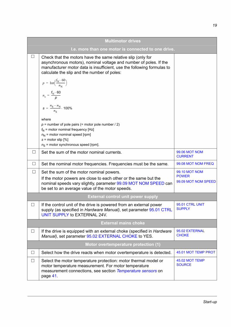
Multimotor drives
I.e. more than one motor is connected to one drive.
Check that the motors have the same relative slip (only for asynchronous motors), nominal voltage and number of poles. If the manufacturer motor data is insufficient, use the following formulas to calculate the slip and the number of poles:
wherep = number of pole pairs (= motor pole number / 2)fN = motor nominal frequency [Hz]nN = motor nominal speed [rpm]s = motor slip [%]nS = motor synchronous speed [rpm].
Set the sum of the motor nominal currents. 99.06 MOT NOM CURRENT
Set the nominal motor frequencies. Frequencies must be the same. 99.08 MOT NOM FREQ
Set the sum of the motor nominal powers.If the motor powers are close to each other or the same but the nominal speeds vary slightly, parameter 99.09 MOT NOM SPEED can be set to an average value of the motor speeds.
99.10 MOT NOM POWER99.09 MOT NOM SPEED
External control unit power supply
If the control unit of the drive is powered from an external power supply (as specified in Hardware Manual), set parameter 95.01 CTRL UNIT SUPPLY to EXTERNAL 24V.
95.01 CTRL UNIT SUPPLY
External mains choke
If the drive is equipped with an external choke (specified in Hardware Manual), set parameter 95.02 EXTERNAL CHOKE to YES.
95.02 EXTERNAL CHOKE
Motor overtemperature protection (1)
Select how the drive reacts when motor overtemperature is detected. 45.01 MOT TEMP PROT
Select the motor temperature protection: motor thermal model or motor temperature measurement. For motor temperature measurement connections, see section Temperature sensors on page 41.
45.02 MOT TEMP SOURCE
snS nN–nS
------------------ 100%⋅=
nsfN 60⋅
p----------------=
p IntfN 60⋅nN---------------⎝ ⎠
⎛ ⎞=
Start-up
20
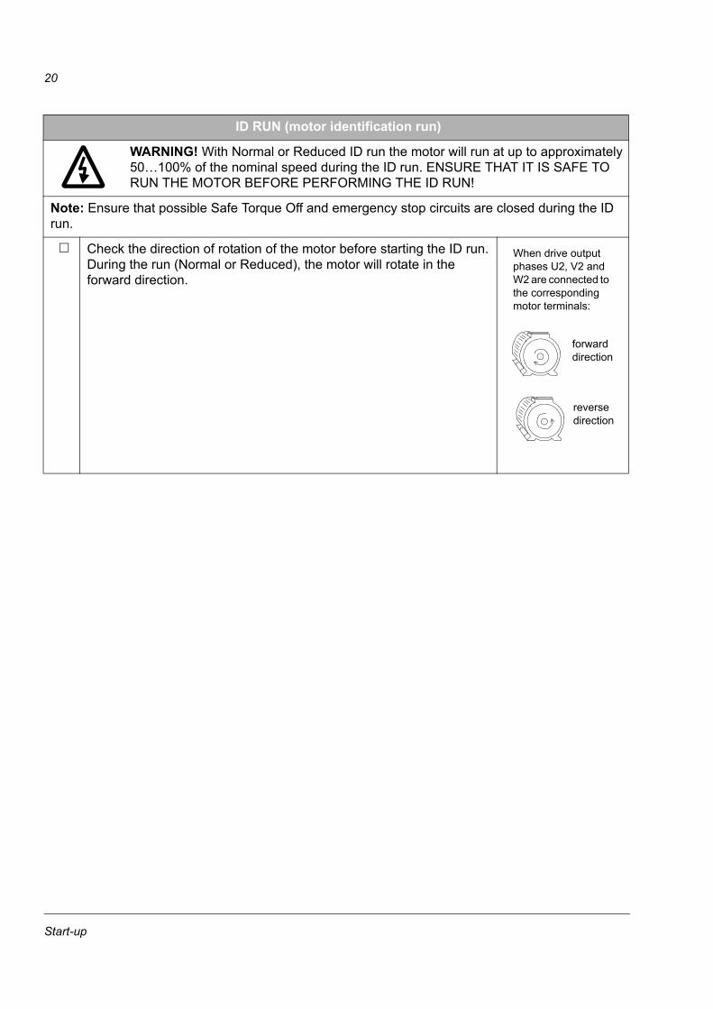
ID RUN (motor identification run)
WARNING! With Normal or Reduced ID run the motor will run at up to approximately 50…100% of the nominal speed during the ID run. ENSURE THAT IT IS SAFE TO RUN THE MOTOR BEFORE PERFORMING THE ID RUN!
Note: Ensure that possible Safe Torque Off and emergency stop circuits are closed during the ID run.
Check the direction of rotation of the motor before starting the ID run. During the run (Normal or Reduced), the motor will rotate in the forward direction.
forward direction
reverse direction
When drive output phases U2, V2 and W2 are connected to the corresponding motor terminals:
Start-up
21
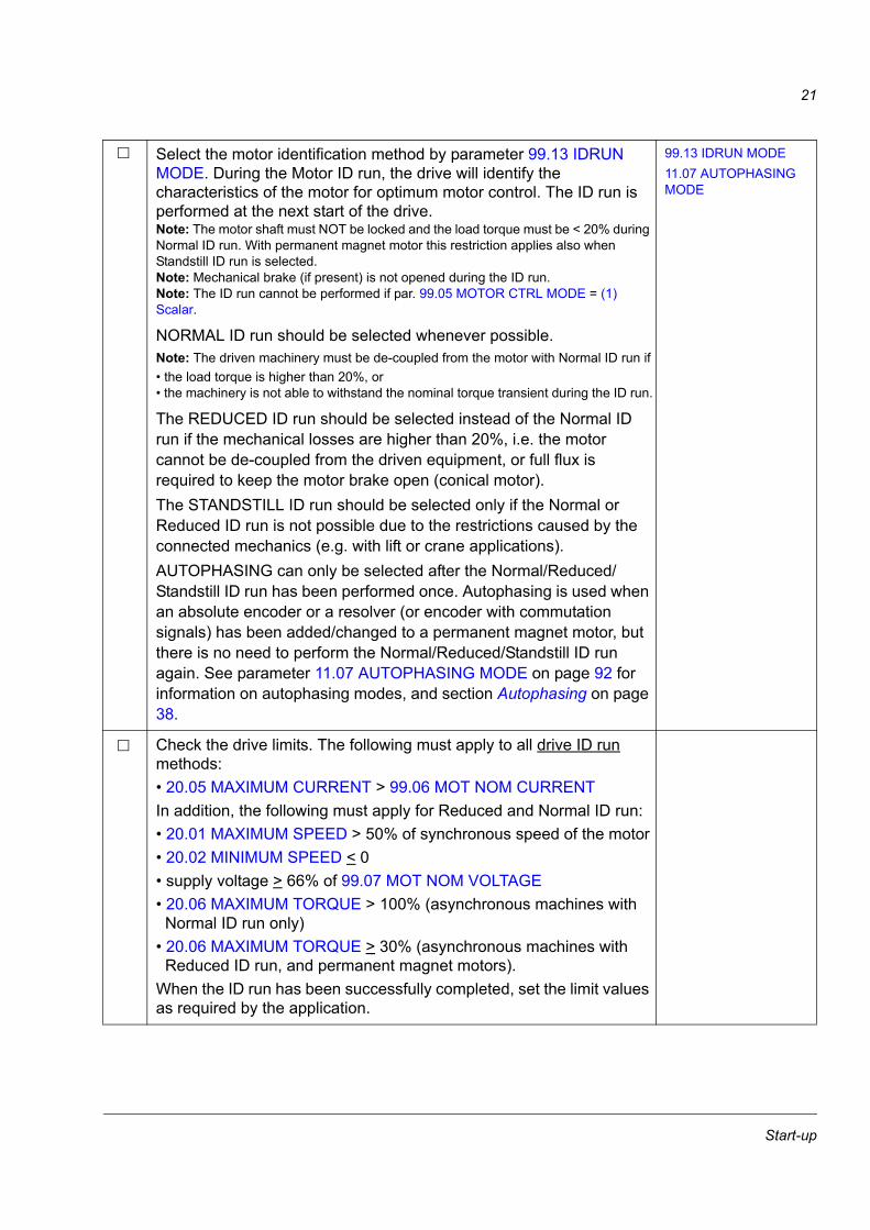
Select the motor identification method by parameter 99.13 IDRUN MODE. During the Motor ID run, the drive will identify the characteristics of the motor for optimum motor control. The ID run is performed at the next start of the drive.Note: The motor shaft must NOT be locked and the load torque must be < 20% during Normal ID run. With permanent magnet motor this restriction applies also when Standstill ID run is selected.Note: Mechanical brake (if present) is not opened during the ID run.Note: The ID run cannot be performed if par. 99.05 MOTOR CTRL MODE = (1) Scalar.
NORMAL ID run should be selected whenever possible.Note: The driven machinery must be de-coupled from the motor with Normal ID run if• the load torque is higher than 20%, or• the machinery is not able to withstand the nominal torque transient during the ID run.
The REDUCED ID run should be selected instead of the Normal ID run if the mechanical losses are higher than 20%, i.e. the motor cannot be de-coupled from the driven equipment, or full flux is required to keep the motor brake open (conical motor).The STANDSTILL ID run should be selected only if the Normal or Reduced ID run is not possible due to the restrictions caused by the connected mechanics (e.g. with lift or crane applications).AUTOPHASING can only be selected after the Normal/Reduced/Standstill ID run has been performed once. Autophasing is used when an absolute encoder or a resolver (or encoder with commutation signals) has been added/changed to a permanent magnet motor, but there is no need to perform the Normal/Reduced/Standstill ID run again. See parameter 11.07 AUTOPHASING MODE on page 92 for information on autophasing modes, and section Autophasing on page 38.
99.13 IDRUN MODE11.07 AUTOPHASING MODE
Check the drive limits. The following must apply to all drive ID run methods:• 20.05 MAXIMUM CURRENT > 99.06 MOT NOM CURRENTIn addition, the following must apply for Reduced and Normal ID run:• 20.01 MAXIMUM SPEED > 50% of synchronous speed of the motor• 20.02 MINIMUM SPEED < 0• supply voltage > 66% of 99.07 MOT NOM VOLTAGE• 20.06 MAXIMUM TORQUE > 100% (asynchronous machines with
Normal ID run only)• 20.06 MAXIMUM TORQUE > 30% (asynchronous machines with
Reduced ID run, and permanent magnet motors).When the ID run has been successfully completed, set the limit values as required by the application.
Start-up
22
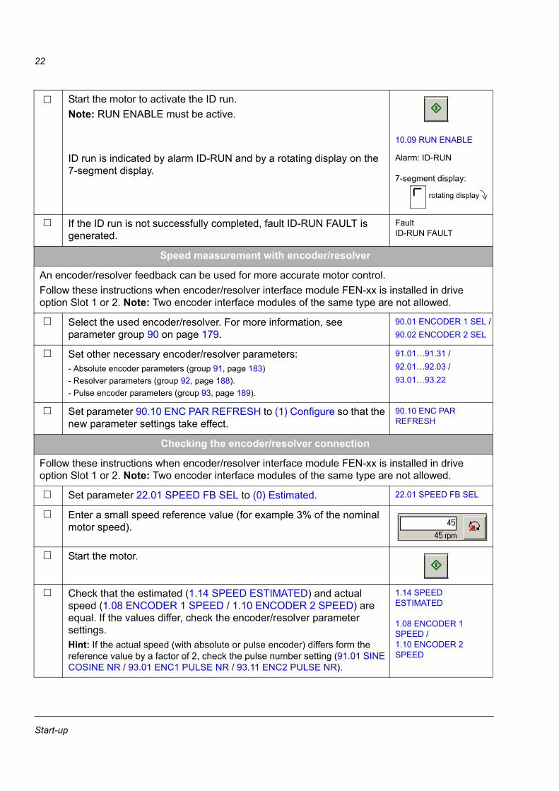
Start the motor to activate the ID run.Note: RUN ENABLE must be active.
10.09 RUN ENABLE
ID run is indicated by alarm ID-RUN and by a rotating display on the 7-segment display.
Alarm: ID-RUN
7-segment display:
If the ID run is not successfully completed, fault ID-RUN FAULT is generated.
FaultID-RUN FAULT
Speed measurement with encoder/resolver
An encoder/resolver feedback can be used for more accurate motor control.Follow these instructions when encoder/resolver interface module FEN-xx is installed in drive option Slot 1 or 2. Note: Two encoder interface modules of the same type are not allowed.
Select the used encoder/resolver. For more information, see parameter group 90 on page 179.
90.01 ENCODER 1 SEL /90.02 ENCODER 2 SEL
Set other necessary encoder/resolver parameters:- Absolute encoder parameters (group 91, page 183)- Resolver parameters (group 92, page 188).- Pulse encoder parameters (group 93, page 189).
91.01…91.31 /92.01…92.03 /93.01…93.22
Set parameter 90.10 ENC PAR REFRESH to (1) Configure so that the new parameter settings take effect.
90.10 ENC PAR REFRESH
Checking the encoder/resolver connection
Follow these instructions when encoder/resolver interface module FEN-xx is installed in drive option Slot 1 or 2. Note: Two encoder interface modules of the same type are not allowed.
Set parameter 22.01 SPEED FB SEL to (0) Estimated. 22.01 SPEED FB SEL
Enter a small speed reference value (for example 3% of the nominal motor speed).
Start the motor.
Check that the estimated (1.14 SPEED ESTIMATED) and actual speed (1.08 ENCODER 1 SPEED / 1.10 ENCODER 2 SPEED) are equal. If the values differ, check the encoder/resolver parameter settings.Hint: If the actual speed (with absolute or pulse encoder) differs form the reference value by a factor of 2, check the pulse number setting (91.01 SINE COSINE NR / 93.01 ENC1 PULSE NR / 93.11 ENC2 PULSE NR).
1.14 SPEED ESTIMATED
1.08 ENCODER 1 SPEED /1.10 ENCODER 2 SPEED
rotating display
Start-up

23
If the direction of rotation is selected as forward, check that the actual speed (1.08 ENCODER 1 SPEED / 1.10 ENCODER 2 SPEED) is positive:• If the actual direction of rotation is forward and the actual speed negative, the phasing of the pulse encoder wires is reversed.• If the actual direction of rotation is reverse and the actual speed negative, the motor cables are incorrectly connected.Changing the connection:Disconnect the main power, and wait for 5 minutes for the intermediate circuit capacitors to discharge. Do the necessary changes. Switch the power on and start the motor again. Check that the estimated and actual speed values are correct.• If the direction of rotation is selected as reverse, the actual speed must be negative.Note: Resolver autotuning routines should always be performed after resolver cable connection has been modified. Autotuning routines can be activated by setting parameter 92.02 EXC SIGNAL AMPL or 92.03 EXC SIGNAL FREQ, and then setting parameter 90.10 ENC PAR REFRESH to (1) Configure. If the resolver is used with a permanent magnet motor, an AUTOPHASING ID run should be performed as well.
1.08 ENCODER 1 SPEED /1.10 ENCODER 2 SPEED
Stop the motor.
Set parameter 22.01 SPEED FB SEL to (1) Enc1 speed or (2) Enc2 speed.If the speed feedback cannot be used in motor control: In special applications parameter 40.06 FORCE OPEN LOOP must be set to TRUE.
22.01 SPEED FB SEL
Note: Speed filtering needs to be adjusted especially when the encoder pulse number is small. See section Speed filtering on page 26.
Emergency stop circuit
If there is an emergency stop circuit in use, check that the circuit functions (emergency stop signal is connected to the digital input which is selected as the source for the emergency stop activation).
10.10 EM STOP OFF3 or 10.11 EM STOP OFF1(emergency stop control through fieldbus 2.12 FBA MAIN CW bits 2…4)
Start-up
24
Safe Torque Off
The Safe Torque Off function disables the control voltage of the power semiconductors of the drive output stage, thus preventing the inverter from generating the voltage required to rotate the motor. For Safe Torque Off wiring, see the appropriate hardware manual and Application guide - Safe torque off function for ACSM1, ACS850 and ACQ810 drives (3AFE68929814 [English]).
If there is a Safe Torque Off circuit in use, check that the circuit functions.
Selects how the drive reacts when the Safe Torque Off function is active (i.e. when the control voltage of the power semiconductors of the drive output stage is disabled).
46.07 STO DIAGNOSTIC
Voltage control
If the DC voltage drops due to input power cut off, the undervoltage controller will automatically decrease the motor torque in order to keep the voltage above the lower limit.To prevent the DC voltage from exceeding the overvoltage control limit, the overvoltage controller automatically decreases the generating torque when the limit is reached. When the overvoltage controller is limiting the generating torque, quick deceleration of the motor is not possible. Thus electrical braking (brake chopper and brake resistor) is needed in some applications to allow the drive to dissipate regenerative energy. The chopper connects the brake resistor to the intermediate circuit of the drive whenever the DC voltage exceeds the maximum limit.
Check that the overvoltage and undervoltage controllers are active. 47.01 OVERVOLTAGE CTRL47.02 UNDERVOLT CTRL
If the application requires a brake resistor (the drive has a built-in brake chopper):• Set the brake chopper and resistor settings.Note: When a brake chopper and resistor are used, the overvoltage controller must be deactivated by parameter 47.01 OVERVOLTAGE CTRL.• Check that the connection functions.For more information on the brake resistor connection, see the appropriate hardware manual.
48.01…48.0747.01 OVERVOLTAGE CTRL
Start-up

25
Start function
Select the start function.Setting 11.01 START MODE to (2) Automatic selects a general-purpose start function. This setting also makes flying start (starting to a rotating motor) possible.The highest possible starting torque is achieved when 11.01 START MODE is set to (0) Fast (automatic optimised DC magnetising) or (1) Const time (constant DC magnetising with user-defined magnetising time).Note: When 11.01 START MODE setting is (0) Fast or (1) Const time, flying start (start to a rotating motor) is not possible.
11.01 START MODE
Limits
Set the operation limits according to the process requirements.Note: If load torque is suddenly lost when the drive is operating in torque control mode, the drive will rush to the defined negative or positive maximum speed. For safe operation, ensure the set limits are suitable for your application.
20.01…20.07
Motor overtemperature protection (2)
Set the alarm and fault limits for the motor overtemperature protection. 45.03 MOT TEMP ALM LIM45.04 MOT TEMP FLT LIM
Set the typical ambient temperature of the motor. 45.05 AMBIENT TEMP
When 45.02 MOT TEMP SOURCE is set to (0) ESTIMATED, the motor thermal protection model must be configured as follows:- Set the maximum allowed operating load of the motor.- Set the zero speed load. A higher value can be used if the motor has an external motor fan to boost the cooling.- Set the break point frequency of the motor load curve.- Set the motor nominal temperature rise.- Set the time inside which the temperature has reached 63% of the nominal temperature.
45.06 MOT LOAD CURVE45.07 ZERO SPEED LOAD45.08 BREAK POINT45.09 MOTNOM TEMP RISE45.10 MOT THERM TIME
If possible, perform the motor ID run again at this point (see page 20). 99.13 IDRUN MODE
Start-up
26
Speed filtering
The measured speed always has a small ripple because of electrical and mechanical interferences, couplings and encoder resolution (i.e. small pulse number). A small ripple is acceptable as long as it does not affect the speed control chain. The interferences in the speed measurement can be filtered with a speed error filter or with an actual speed filter. Reducing the ripple with filters may cause speed controller tuning problems. A long filter time constant and fast acceleration time contradict one another. A very long filter time results in unstable control.
If the used speed reference changes rapidly (servo application), use the speed error filter to filter the possible interferences in the speed measurement. In this case the speed error filter is more suitable than the actual speed filter: - Set the filter time constant.
26.06 SPD ERR FTIME
If the used speed reference remains constant, use the actual speed filter to filter the possible interferences in the speed measurement. In this case the actual speed filter is more suitable than the speed error filter:- Set the filter time constant. If there are substantial interferences in the speed measurement, the filter time constant should be proportional to the total inertia of the load and motor, i.e. approximately 10…30% of the mechanical time constant tmech = (nnom / Tnom) × Jtot × 2π / 60, whereJtot = total inertia of the load and motor (the gear ratio between the load and the motor must be taken into account)nnom = motor nominal speedTnom = motor nominal torqueTo get a fast dynamic torque or speed response with a speed feedback value other than (0) Estimated (see parameter 22.01 SPEED FB SEL), the actual speed filter time must be set to zero.
22.02 SPEED ACT FTIME
Speed controller tuning
For the most demanding applications, the P- and I-parts of the speed controller of the drive can be tuned either manually or automatically. See parameter 28.16 PI TUNE MODE.If it is necessary to adjust acceleration (deceleration) compensation, it must be done manually.
Acceleration (deceleration) compensation can be used to improve the speed control dynamic reference change (when the speed ramp times > 0). In order to compensate inertia during acceleration, a derivative of the speed reference is added to the output of the speed controller.Set the derivation time for acceleration (deceleration) compensation. The value should be proportional to the total inertia of the load and motor, i.e. approximately 50…100% of the mechanical time constant (tmech). See the mechanical time constant equation in section Speed filtering on page 26.
26.08 ACC COMP DERTIME
Start-up
27
Fieldbus control
Follow these instructions when the drive is controlled from a fieldbus control system via fieldbus adapter Fxxx. The adapter is installed in drive Slot 3.
Enable the communication between the drive and fieldbus adapter. 50.01 FBA ENABLE
Connect the fieldbus control system to the fieldbus adapter module.
Set the communication and adapter module parameters: See section Setting up communication through a fieldbus adapter module on page 338.
Test that the communication functions.
Start-up

28
How to control the drive through the I/O interfaceThe table below instructs how to operate the drive through the digital and analogue inputs, when the default parameter settings are valid.
PRELIMINARY SETTINGS
Ensure the control connections are wired according to the connection diagram given in chapter Default connections of the control unit.
Switch to external control by clicking the Take/Release button of the PC tool control panel.
STARTING AND CONTROLLING THE SPEED OF THE MOTOR
Start the drive by switching digital input DI1 on. Digital input status can be monitored with signal 2.01 DI STATUS.
2.01 DI STATUS
Check that analogue input AI1 is used as a voltage input (selected by jumper J1).
Regulate the speed by adjusting the voltage of analogue input AI1.
Check analogue input AI1 signal scaling. AI1 values can be monitored with signals 2.04 AI1 and 2.05 AI1 SCALED.When AI1 is used as a voltage input, the input is differential and the negative value corresponds to the negative speed and the positive value to the positive speed.
13.02…13.042.04 AI12.05 AI1 SCALED
STOPPING THE MOTOR
Stop the drive by switching digital input DI1 off. 2.01 DI STATUS
Voltage:
J1
Start-up

29
Drive programming using PC tools
What this chapter containsThis chapter introduces the drive programming using the DriveStudio and DriveSPC applications. For more information, see DriveStudio User Manual [3AFE68749026 (English)] and DriveSPC User Manual [3AFE68836590 (English)].
GeneralThe drive control program is divided into two parts:
• firmware program
• application program.
The firmware program performs the main control functions, including speed and torque control, drive logic (start/stop), I/O, feedback, communication and protection functions. Firmware functions are configured and programmed with parameters. The functions of the firmware program can be extended with application programming. Application programs are built out of function blocks.
The drive supports two different programming methods:
• parameter programming
• application programming with function blocks (the blocks are based on the IEC-61131 standard).
M
Application program Firmware
E
Speed control Torque controlDrive logicI/O interfaceFieldbus interfaceProtectionsFeedback
Standard block library
Function block program
Drive control program
Technology block library
Firmware blocks (parameter and signal interface)
Drive programming using PC tools
30
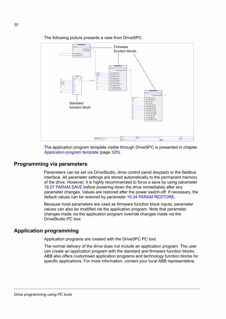
The following picture presents a view from DriveSPC.
The application program template visible through DriveSPC is presented in chapter Application program template (page 325).
Programming via parametersParameters can be set via DriveStudio, drive control panel (keypad) or the fieldbus interface. All parameter settings are stored automatically to the permanent memory of the drive. However, it is highly recommended to force a save by using parameter 16.07 PARAM SAVE before powering down the drive immediately after any parameter changes. Values are restored after the power switch-off. If necessary, the default values can be restored by parameter 16.04 PARAM RESTORE.
Because most parameters are used as firmware function block inputs, parameter values can also be modified via the application program. Note that parameter changes made via the application program override changes made via the DriveStudio PC tool.
Application programmingApplication programs are created with the DriveSPC PC tool.
The normal delivery of the drive does not include an application program. The user can create an application program with the standard and firmware function blocks. ABB also offers customised application programs and technology function blocks for specific applications. For more information, contact your local ABB representative.
SPEED REF SEL3
TL2 250 µsec (1)
24.01 SPEED REF1 SEL1
24.02 SPEED REF2 SEL0
3.01 SPEED REF1
3.02 SPEED REF2
SPEED REF MOD4
TL3 250 µsec (1)
< 24.03 SPEED REF1 INO UTPUT(44)
(6 / 44)
< 24.04 SPEED REF2 INSPEED REF2
(6 / 3.02)
< 24.05 SPD REF 1/2 SELFA LSE
24.06 SPEED SHARE1.000
< 24.07 SPD REF NEG ENAFA LSE
24.08 CONST SPEED0
rpm
< 24.09 CONST SPEED ENAFA LSE
24.10 SPEED REF JOG10
rpm
24.11 SPEED REF JOG20rpm
24.12 SPEED REFMIN ABS0rpm
3.03 SPEEDREF RAMP IN
SPEED REF RAMP31
TL7 500 µsec (18)
< 25.01 SPEED RAMP INSPEEDREF RAMP IN(6 / 3.03)
25.02 SPEED SCALING1500rpm
25.03 ACC TIME1.000
s
25.04 DEC TIME1.000
s
25.05 SHAPE TIME ACC10.000
s
25.06 SHAPE TIME ACC20.000
s
25.07 SHAPE TIME DEC10.000
s
25.08 SHAPE TIME DEC20.000
s
25.09 ACC TIME JOGGING0.000
s
25.10 DEC TIME JOGGING0.000
s
25.11 EM STOP TIME1.000s
25.12 SPEEDREF BAL0.000rpm
< 25.13 SPEEDREF BAL ENAFA LSE
3.04 SPEEDREF RAMPED
MOTPOT44
TL9 10 msec (1)
ENA BLETRUE
UPDI STATUS.4
(2 / 2.01.DI5)
DO WNDI STATUS.5
(2 / 2.01.DI6)
RAMPTIME10
MA XV A L1000
MINV AL0
RESETVA L0
RESETFA LSE
O UTPUTOUTPUT(44)
Page 6 Speed RefF irmware Library ID = 1, v er = 1.0Standard Library ID = 10000, v er = 1.0
Based onCustomer
Cust. Doc. No.Date
PreparedA pprov edProject name
Title Doc. des.
Resp. dept.Doc. No.
Standard function block
Firmwarefunction blocks
Drive programming using PC tools
31
Function blocksThe application program uses three types of function blocks: firmware function blocks, standard function blocks and technology function blocks.
Firmware function blocks
Most of the firmware functions are represented as function blocks in the DriveSPC tool. Firmware function blocks are part of the drive control firmware, and used as an interface between the application and firmware programs. Drive parameters in groups 10…99 are used as function block inputs and parameters in groups 1…9 as function block outputs. Firmware function blocks are presented in chapter Parameters and firmware blocks.
Standard function blocks (library)
Standard function blocks (e.g. ADD, AND) are used to create an executable application program. The standard function blocks available are presented in chapter Standard function blocks.
Standard function block library is always included in the drive delivery.
Technology function blocks
Several technology function block libraries (e.g. CAM) are available for different types of applications. One technology library can be used at a time. Technology blocks are used in a similar way as the standard blocks.
User parametersUser parameters can be created with the DriveSPC tool. They are inserted into the application program as blocks that can be connected to existing application blocks.
User parameters can be added to any existing parameter group; the first available index is 70. Parameter groups 5 and 75…89 are available for user parameters starting from index 1. Using attributes, the parameters can be defined as write-protected, hidden, etc.
For more information, see the DriveSPC User Manual.
Application eventsThe application programmer can create his/her own application events (alarms and faults) by adding alarm and fault blocks; these blocks are managed through the Alarm and Fault Managers of the DriveSPC tool.
The operation of alarm and fault blocks is the same: when the block is enabled (by setting the Enable input to 1), an alarm or fault is generated by the drive.
Program executionThe application program is loaded to the permanent (non-volatile) memory of the memory unit (JMU). When the loading finishes, the drive control board is automatically reset, and the downloaded program started. The program is executed in real time on the same Central Processing Unit (CPU of the drive control board) as the drive firmware. The program can be executed at the two dedicated time levels of 1 and 10 milliseconds, as well as other time levels between certain firmware tasks.
Drive programming using PC tools
32
Note: Because the firmware and application programs use the same CPU, the programmer must ensure that the drive CPU is not overloaded. See parameter 1.21 CPU USAGE.
Application program licensing and protectionNote: This functionality is only available with DriveSPC version 1.5 and later.
The drive can be assigned an application licence consisting of an ID and password using the DriveSPC tool. Likewise, the application program created in DriveSPC can be protected by an ID and password. For instructions, refer to the DriveSPC user manual.
If a protected application program is downloaded to a licensed drive, the IDs and passwords of the application and drive must match. A protected application cannot be downloaded to an unlicensed drive. On the other hand, an unprotected application can be downloaded to a licensed drive.
The ID of the application licence is displayed by DriveStudio in the drive software properties as APPL LICENCE. If the value is 0, no licence has been assigned to the drive.
The parameters that are created using the DriveSPC parameter manager with hide flags can be viewed or hidden by parameter 16.03 PASS CODE. The password code must be the same as the drive APPL LICENCE. A wrong password code will hide the visible application parameters again.
Notes:• The application licence can only be assigned to a complete drive, not a stand-
alone control unit.
• A protected application can only be downloaded to a complete drive, not a stand-alone control unit.
Operation modesThe DriveSPC tool offers the following operation modes:
Off-line
When the off-line mode is used without a drive connection, the user can
• open a application program file (if exists).
• modify and save the application program.
• print the program pages.
When the off-line mode is used with a drive(s) connection, the user can
• connect the selected drive to DriveSPC.
• upload an application program from the connected drive (an empty template which includes only the firmware blocks is available by default.)
• download the configured application program to the drive and start the program execution. The downloaded program contains the function block program and the parameter values set in DriveSPC.
Drive programming using PC tools

33
• remove the program from the connected drive.
On-line
In the on-line mode, the user can
• modify firmware parameters (changes are stored directly to the drive memory)
• modify application program parameters (i.e. parameters created in DriveSPC)
• monitor the actual values of all function blocks in real time.
Drive programming using PC tools

34
Drive programming using PC tools

35
Drive control and features
What this chapter containsThis chapter describes the control locations and operation modes of the drive, and the features of the application program.
Local control vs. external controlThe drive has two main control locations: external and local. The control location is selected with the PC tool (Take/Release button) or with the LOC/REM key on the control panel.
Local control
The control commands are given from a PC equipped with DriveStudio and/or DriveSPC, or from the control panel keypad when the drive is in local control. Speed, torque and position control modes are available for local control.
PC tool (DriveStudio/DriveSPC)or
Control panel (optional)
1) Extra inputs/outputs can be added by installing optional I/O extension modules (FIO-xx) in drive Slot 1/2.2) Incremental or absolute encoder, or resolver interface module (FEN-xx) installed in drive Slot 1/23) Two encoder/resolver interface modules of the same type are not allowed.
MOTOR
PLC (= Programmable Logic Controller)
M3~
External control
I/O 1) 3)
Drive-to-drive link
Fieldbus adapterFxxx in Slot 3
Encoder
Local control
ACSM1
2) 3)
Drive control and features

36
Local control is mainly used during commissioning and maintenance. The control panel always overrides the external control signal sources when used in local control. Changing the control location to local can be disabled by parameter 16.01 LOCAL LOCK.
The user can select by a parameter (46.03 LOCAL CTRL LOSS) how the drive reacts to a control panel or PC tool communication break.
External control
When the drive is in external control, control commands (start/stop, reset etc.) are given through the fieldbus interface (via an optional fieldbus adapter module), the I/O terminals (digital inputs), optional I/O extension modules or the drive-to-drive link.
Two external control locations, EXT1 and EXT2, are available. The user can select control signals (e.g. Group 10 START/STOP, Group 24 SPEED REF MOD and Group 32 TORQUE REFERENCE) and control modes (Group 34 REFERENCE CTRL) for both external control locations. Depending on the user selection, either EXT1 or EXT2 is active at a time. Selection between EXT1/EXT2 is done via a freely selectable bit pointer parameter 34.01 EXT1/EXT2 SEL. In addition, the EXT1 control location is divided into two parts, EXT1 CTRL MODE1 and EXT1 CTRL MODE2. Both use the EXT1 control signals for start/stop, but the control mode can be different; for example, EXT1 CTRL MODE2 can be used in homing.
Operating modes of the driveThe drive can operate in speed and torque control modes. A block diagram of the drive control chain for these modes is presented on page 37; more detailed diagrams are presented in Appendix C – Control chain and drive logic diagrams (page 355).
Speed control modeMotor rotates at a speed proportional to the speed reference given to the drive. This mode can be used either with estimated speed used as feedback, or with an encoder or resolver for better speed accuracy.
Speed control mode is available in both local and external control.
Torque control modeMotor torque is proportional to the torque reference given to the drive. This mode can be used either with estimated speed used as feedback, or with an encoder or resolver for more accurate and dynamic motor control.
Torque control mode is available in both local and external control.
Drive control and features
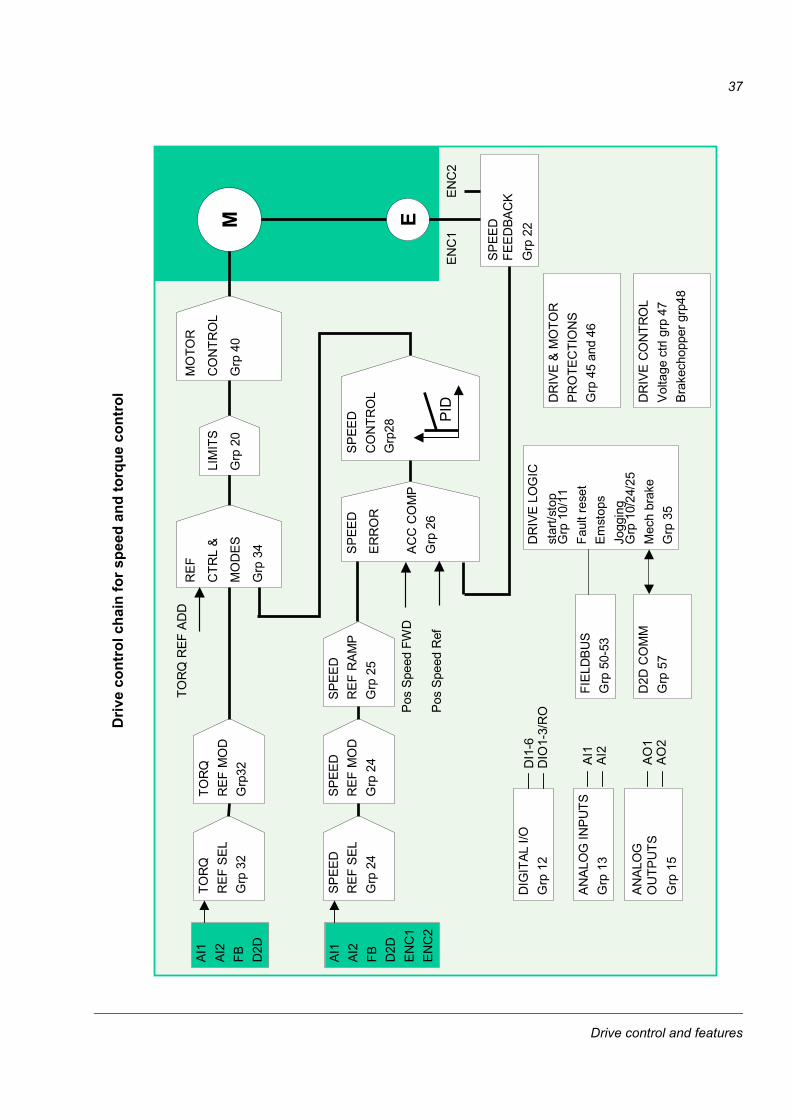
37
��
���
�
��
���
�
��
�� �
���
��
����
��
��
��
����
��
��
���
�
��
��
����
��
����
��
��
��
����
��
����
�
����
���
��
����
�
����
�
��
���
����
�
����
��
���
���
��
����
����
�����
����
��
����
���
!"���
#�#�
�$��
��
% &&
'(&�
������
���
����
�� �
�)�
#*+�
,��-
#�
���)
��
����
.��
���
���
���
���
��
�
���
)��(
/� 0
���
�
���
�.
��
���
��
��
���
�12
�
���)
�3)�
����
��
����
���
��
��)
����
��
���
��
���
���
��
��
��0
���
���
����
��
����
��
����
1��
4
����
�
���
���
��
��
�)5
���
�
����2
��
����
�
���
�
��
2��
2��
��
��)
���
30�
���3
���
�
���
���
���
���
��
����
��
���
�
� "��
&#�*
��"�&
���
5�1�
�-#*
+ ��
#��&
�� �
���
���
�1 ���
���
���
��
���
���
�1 ���
���
���
��
��
���
��
��
���
� ��
��##
/��
#6
� ��
��##
/��7
�
Driv
e co
ntro
l cha
in fo
r spe
ed a
nd to
rque
con
trol
Drive control and features

38
Motor control features
Scalar motor controlIt is possible to select scalar control as the motor control method instead of Direct Torque Control (DTC). In scalar control mode, the drive is controlled with a frequency reference. However, the performance of DTC is not achieved in scalar control.
It is recommended to activate the scalar motor control mode in the following situations:
• In multimotor drives: 1) if the load is not equally shared between the motors, 2) if the motors are of different sizes, or 3) if the motors are going to be changed after motor identification (ID run)
• If the nominal current of the motor is less than 1/6 of the nominal output current of the drive
• If the drive is used without a motor connected (for example, for test purposes)
• If the drive runs a medium-voltage motor through a step-up transformer.
In scalar control, some standard features are not available.
IR compensation for a scalar controlled drive
IR stands for voltage.
I (current) × R (resistance) = U (voltage).
IR compensation is active only when the motor control mode is scalar. When IR compensation is activated, the drive gives an extra voltage boost to the motor at low speeds. IR compensation is useful in applications that require a high break-away torque.
In direct torque control (DTC) mode, IR compensation is automatic and manual adjustment is not needed.
AutophasingAutophasing is an automatic measurement routine to determine the angular position of the magnetic flux of a permanent magnet synchronous motor. The motor control requires the absolute position of the rotor flux in order to control motor torque accurately.
Sensors like absolute encoders and resolvers indicate the rotor position at all times after the offset between the zero angle of rotor and that of the sensor has been established. On the other hand, a standard pulse encoder determines the rotor position when it rotates but the initial position is not known. However, a pulse encoder can be used as an absolute encoder if it is equipped with Hall sensors, albeit with coarse initial position accuracy. The Hall sensors generate so-called commutation pulses that change their state six times during one revolution, so it is only known within which 60° sector of a complete revolution the initial position is.
f (Hz)
Motor voltage
No compensation
IR Compensation
50% of nominal frequency
Drive control and features
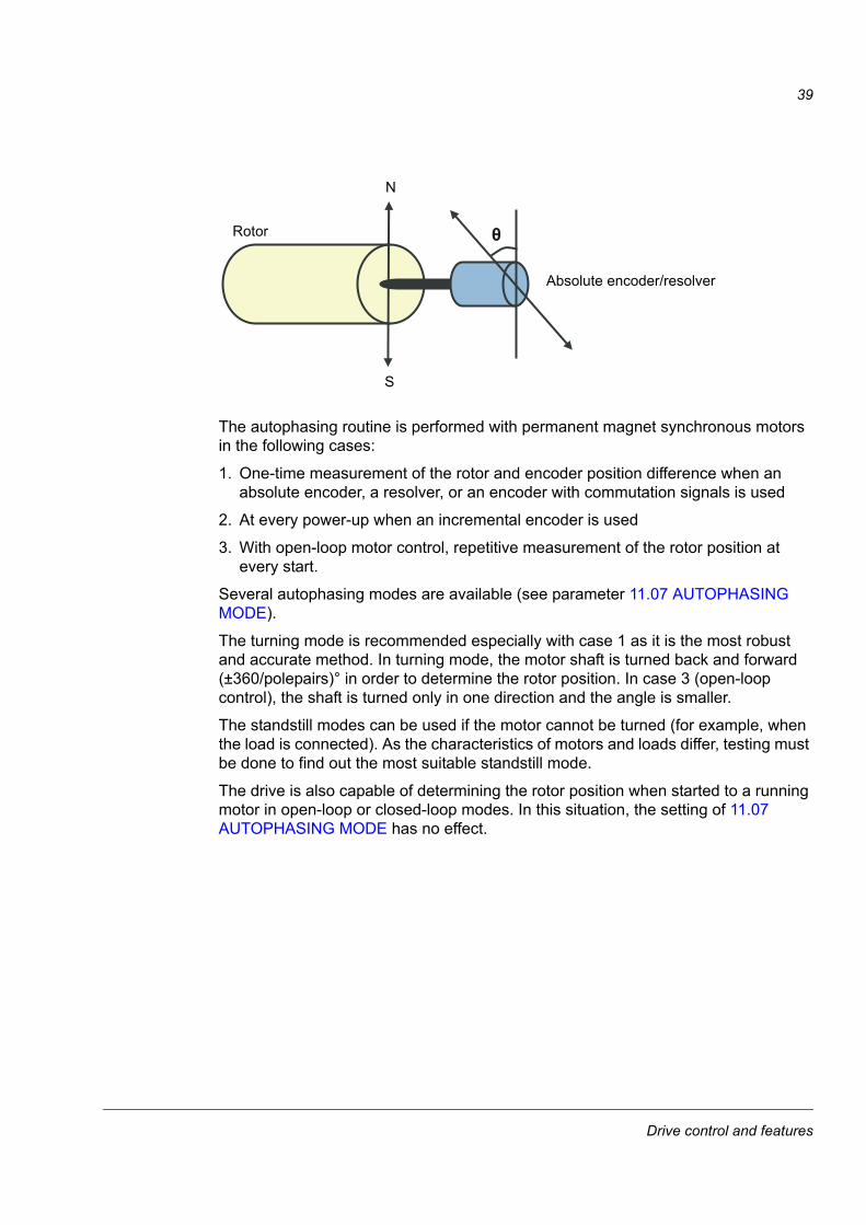
39
The autophasing routine is performed with permanent magnet synchronous motors in the following cases:
1. One-time measurement of the rotor and encoder position difference when an absolute encoder, a resolver, or an encoder with commutation signals is used
2. At every power-up when an incremental encoder is used
3. With open-loop motor control, repetitive measurement of the rotor position at every start.
Several autophasing modes are available (see parameter 11.07 AUTOPHASING MODE).
The turning mode is recommended especially with case 1 as it is the most robust and accurate method. In turning mode, the motor shaft is turned back and forward (±360/polepairs)° in order to determine the rotor position. In case 3 (open-loop control), the shaft is turned only in one direction and the angle is smaller.
The standstill modes can be used if the motor cannot be turned (for example, when the load is connected). As the characteristics of motors and loads differ, testing must be done to find out the most suitable standstill mode.
The drive is also capable of determining the rotor position when started to a running motor in open-loop or closed-loop modes. In this situation, the setting of 11.07 AUTOPHASING MODE has no effect.
�
Absolute encoder/resolver
Rotor
N
S
Drive control and features

40
Flux brakingThe drive can provide greater deceleration by raising the level of magnetization in the motor. By increasing the motor flux with 40.10 FLUX BRAKING, the energy generated by the motor during braking can be converted to motor thermal energy.
The drive monitors the motor status continuously, also during flux braking. Therefore, flux braking can be used both for stopping the motor and for changing the speed. The other benefits of flux braking are:
• The braking starts immediately after a stop command is given. The function does not need to wait for the flux reduction before it can start the braking.
• The cooling of the induction motor is efficient. The stator current of the motor increases during flux braking, not the rotor current. The stator cools much more efficiently than the rotor.
• Flux braking can be used with induction motors and permanent magnet synchronous motors.
Two braking power levels are available:
• Moderate braking provides faster deceleration compared to a situation where flux braking is disabled. The flux level of the motor is limited to prevent excessive heating of the motor.
• Full braking exploits almost all available current to convert the mechanical braking energy to motor thermal energy. Braking time is shorter compared to moderate braking. In cyclic use, motor heating may be significant.
Thermal motor protectionWith the parameters in group 45, the user can set up the motor overtemperature protection and configure motor temperature measurement (if present). This block also shows the estimated and measured motor temperature.
The motor can be protected against overheating by
• the motor thermal protection model
• measuring the motor temperature with PTC or KTY84 sensors. This will result in a more accurate motor model.
TBrTN
20
40
60
(%)Motor speed
No flux braking
Flux braking
TBr = Braking torqueTN = 100 Nm
Flux braking
No flux brakingt (s) f (Hz)
Drive control and features
41
Thermal motor protection model
The drive calculates the temperature of the motor on the basis of the following assumptions:
1) When power is applied to the drive for the first time, the motor is at ambient temperature (defined by parameter 45.05 AMBIENT TEMP). After this, when power is applied to the drive, the motor is assumed to be at the estimated temperature (value of 1.18 MOTOR TEMP EST, saved at power switch-off).
2) Motor temperature is calculated using the user-adjustable motor thermal time and motor load curve. The load curve should be adjusted in case the ambient temperature exceeds 30 °C.
It is possible to adjust the motor temperature supervision limits and select how the drive reacts when overtemperature is detected.
Note: The motor thermal model can be used when only one motor is connected to the inverter.
Temperature sensors
It is possible to detect motor overtemperature by connecting a motor temperature sensor to thermistor input TH of the drive or to optional encoder interface module FEN-xx.
The resistance of the sensor increases as the motor temperature rises over the sensor reference temperature Tref, as does the voltage over the resistor.
The figure below shows typical PTC sensor resistance values as a function of the motor operating temperature.
100
550
1330
4000
Ohm
T
Temperature PTC resistanceNormal 0…1 kohm
Excessive > 4 kohm*
*The limit for overtemperature protection is 2.5 kohm.
Drive control and features
42
The figure below shows typical KTY84 sensor resistance values as a function of the motor operating temperature.
It is possible to adjust the motor temperature supervision limits and select how the drive reacts when overtemperature is detected.
WARNING! As the thermistor input on the JCU Control Unit is not insulated according to IEC 60664, the connection of the motor temperature sensor requires double or reinforced insulation between motor live parts and the sensor. If the assembly does not fulfil the requirement,- the I/O board terminals must be protected against contact and must not be connected to other equipmentor- the temperature sensor must be isolated from the I/O terminals.
The figure below shows a motor temperature measurement when thermistor input TH is used.
1000
2000
3000ohm
T (°C)
KTY84 scaling90 °C = 936 ohm110 °C = 1063 ohm130 °C = 1197 ohm150 °C = 1340 ohm
-1000
0 100 200 300
Motor
T
JCU Control Unit
TH
AGND
10 nF
One PTC or KTY84 sensor
Motor
T
JCU Control Unit
TH
AGND
TT
Three PTC sensors
10 nF
Drive control and features

43
For encoder interface module FEN-xx connection, see the User’s Manual of the appropriate encoder interface module.
Drive control and features
44
DC voltage control features
Overvoltage controlOvervoltage control of the intermediate DC link is needed with two-quadrant line-side converters when the motor operates within the generating quadrant. To prevent the DC voltage from exceeding the overvoltage control limit, the overvoltage controller automatically decreases the generating torque when the limit is reached.
Undervoltage controlIf the incoming supply voltage is cut off, the drive will continue to operate by utilising the kinetic energy of the rotating motor. The drive will be fully operational as long as the motor rotates and generates energy to the drive. The drive can continue the operation after the break if the main contactor remained closed.
Note: Units equipped with main contactor option must be equipped with a hold circuit (e.g. UPS) which keeps the contactor control circuit closed during a short supply break.
Voltage control and trip limitsThe control and trip limits of the intermediate DC voltage regulator are relative either to a supply voltage value provided by the user or to an automatically-determined supply voltage. The actual voltage used is shown by parameter 1.19 USED SUPPLY VOLT. The DC voltage (UDC) equals 1.35 times this value.
130
260
390
520
1.6 4.8 8 11.2 14.4t(s)
UDC
fout
TM
UDC= intermediate circuit voltage of the drive, fout = output frequency of the drive,TM = motor torqueLoss of supply voltage at nominal load (fout = 40 Hz). The intermediate circuit DC voltage drops to the minimum limit. The controller keeps the voltage steady as long as the supply is switched off. The drive runs the motor in generator mode. The motor speed falls but the drive is operational as long as the motor has enough kinetic energy.
Umains
20
40
60
80
40
80
120
160
TM
(Nm)
fout
(Hz)
UDC
(VDC)
Drive control and features
45
Automatic identification of the supply voltage is performed every time the drive is powered. Automatic identification can be disabled by parameter 47.03 SUPPLVOLTAUTO-ID; the user can define the voltage manually at parameter 47.04 SUPPLY VOLTAGE.
The intermediate DC circuit is charged over an internal resistor which is bypassed when the capacitors are considered charged and the voltage has stabilized.
Brake chopperThe built-in brake chopper of the drive can be used to handle the energy generated by a decelerating motor.
When the brake chopper is enabled and a resistor connected, the chopper will start conducting when the DC link voltage of the drive reaches UDC_BR - 30 V. The maximum braking power is achieved at UDC_BR + 30 V.
UDC_BR = 1.35 × 1.25 × 1.19 USED SUPPLY VOLT.
Low voltage modeA Low voltage mode is available to extend the supply voltage range. When the mode is enabled, the drive can operate below the nominal range, for example when it needs to be powered from an emergency supply.
Low voltage mode can be activated by parameter 47.05 LOW VOLT MOD ENA. Low voltage mode introduces parameters 47.06 LOW VOLT DC MIN and 47.07 LOW VOLT DC MAX for adjustment of minimum and maximum DC voltage control levels respectively. The following rules apply:
• 47.06 LOW VOLT DC MIN = 250 to 450 V• 47.07 LOW VOLT DC MAX = 350 to 810 V• 47.07 LOW VOLT DC MAX > 47.06 LOW VOLT DC MIN + 50 V.
1.07 DC-VOLTAGE
Undervoltage control level (0.8 × UDC; 400 V min.)
Undervoltage trip level (UDC, low - 50 V; 350 V min.)
Overvoltage control level (1.25 × UDC; 810 V max.)
Overvoltage fault level (UDC, high + 70 V; 880 V max.)
UDC = 1.35 × 1.19 USED SUPPLY VOLT
UDC, high = 1.25 × UDC
UDC, low = 0.8 × UDC
Drive control and features
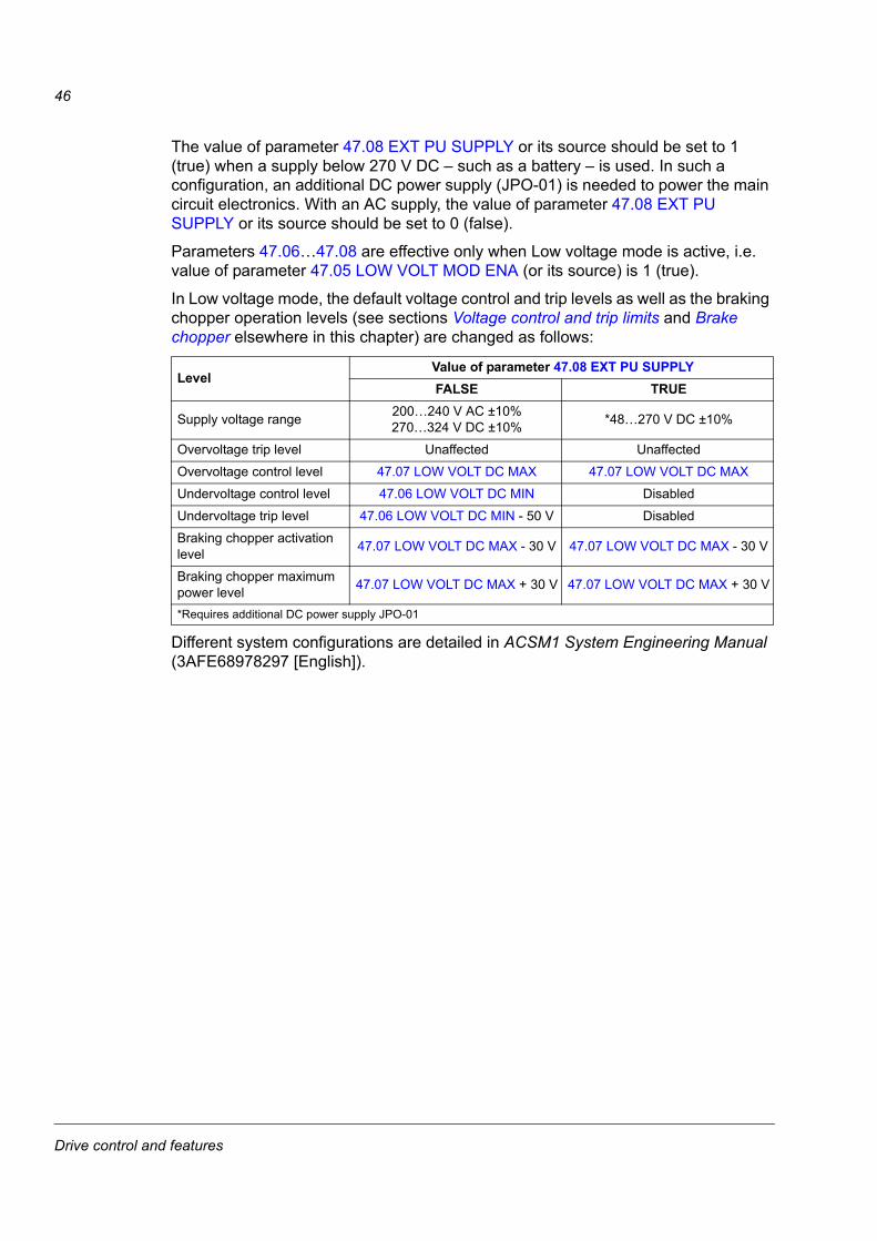
46
The value of parameter 47.08 EXT PU SUPPLY or its source should be set to 1 (true) when a supply below 270 V DC – such as a battery – is used. In such a configuration, an additional DC power supply (JPO-01) is needed to power the main circuit electronics. With an AC supply, the value of parameter 47.08 EXT PU SUPPLY or its source should be set to 0 (false).
Parameters 47.06…47.08 are effective only when Low voltage mode is active, i.e. value of parameter 47.05 LOW VOLT MOD ENA (or its source) is 1 (true).
In Low voltage mode, the default voltage control and trip levels as well as the braking chopper operation levels (see sections Voltage control and trip limits and Brake chopper elsewhere in this chapter) are changed as follows:
Different system configurations are detailed in ACSM1 System Engineering Manual (3AFE68978297 [English]).
LevelValue of parameter 47.08 EXT PU SUPPLYFALSE TRUE
Supply voltage range 200…240 V AC ±10%270…324 V DC ±10% *48…270 V DC ±10%
Overvoltage trip level Unaffected Unaffected
Overvoltage control level 47.07 LOW VOLT DC MAX 47.07 LOW VOLT DC MAX
Undervoltage control level 47.06 LOW VOLT DC MIN Disabled
Undervoltage trip level 47.06 LOW VOLT DC MIN - 50 V Disabled
Braking chopper activation level 47.07 LOW VOLT DC MAX - 30 V 47.07 LOW VOLT DC MAX - 30 V
Braking chopper maximum power level 47.07 LOW VOLT DC MAX + 30 V 47.07 LOW VOLT DC MAX + 30 V
*Requires additional DC power supply JPO-01
Drive control and features
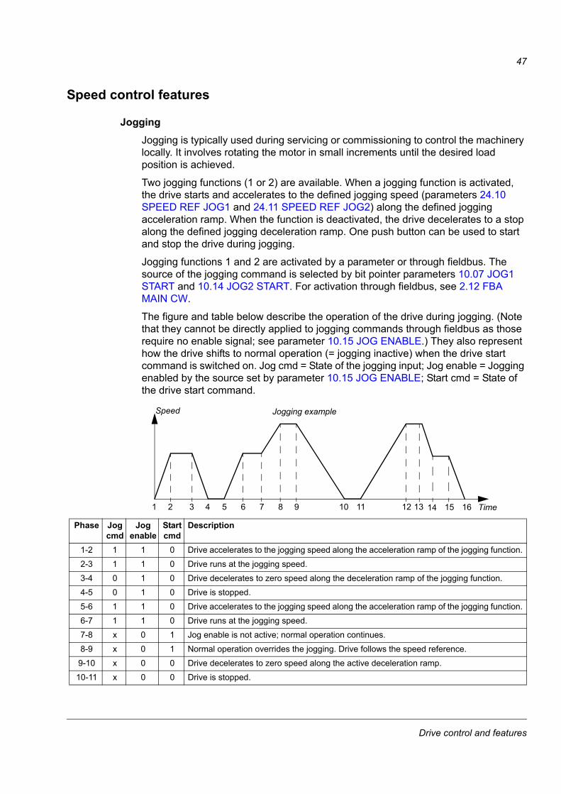
47
Speed control features
JoggingJogging is typically used during servicing or commissioning to control the machinery locally. It involves rotating the motor in small increments until the desired load position is achieved.
Two jogging functions (1 or 2) are available. When a jogging function is activated, the drive starts and accelerates to the defined jogging speed (parameters 24.10 SPEED REF JOG1 and 24.11 SPEED REF JOG2) along the defined jogging acceleration ramp. When the function is deactivated, the drive decelerates to a stop along the defined jogging deceleration ramp. One push button can be used to start and stop the drive during jogging.
Jogging functions 1 and 2 are activated by a parameter or through fieldbus. The source of the jogging command is selected by bit pointer parameters 10.07 JOG1 START and 10.14 JOG2 START. For activation through fieldbus, see 2.12 FBA MAIN CW.
The figure and table below describe the operation of the drive during jogging. (Note that they cannot be directly applied to jogging commands through fieldbus as those require no enable signal; see parameter 10.15 JOG ENABLE.) They also represent how the drive shifts to normal operation (= jogging inactive) when the drive start command is switched on. Jog cmd = State of the jogging input; Jog enable = Jogging enabled by the source set by parameter 10.15 JOG ENABLE; Start cmd = State of the drive start command.
Phase Jog cmd
Jog enable
Start cmd
Description
1-2 1 1 0 Drive accelerates to the jogging speed along the acceleration ramp of the jogging function.
2-3 1 1 0 Drive runs at the jogging speed.
3-4 0 1 0 Drive decelerates to zero speed along the deceleration ramp of the jogging function.
4-5 0 1 0 Drive is stopped.
5-6 1 1 0 Drive accelerates to the jogging speed along the acceleration ramp of the jogging function.
6-7 1 1 0 Drive runs at the jogging speed.
7-8 x 0 1 Jog enable is not active; normal operation continues.
8-9 x 0 1 Normal operation overrides the jogging. Drive follows the speed reference.
9-10 x 0 0 Drive decelerates to zero speed along the active deceleration ramp.
10-11 x 0 0 Drive is stopped.
Time
Speed
1 2 3 4 5 6 7 8 9 10 11 12 13 14 15 16
Jogging example
Drive control and features
48
Notes:• Jogging is not operational when the drive start command is on, or when the drive
is in local control.
• Normal start is inhibited when jog enable is active.
• The ramp shape time is set to zero during jogging.
Speed controller tuningThe speed controller of the drive can be automatically adjusted using the autotune function (parameter 28.16 PI TUNE MODE). Autotuning is based on the load and inertia of the motor and the machine. It is, however, also possible to manually adjust the controller gain, integration time and derivation time. Autotuning can also be performed from an external control location.
Autotuning can be performed in four different ways depending on the setting of parameter 28.16 PI TUNE MODE. The selections (1) Smooth, (2) Middle and (3) Tight define how the drive torque reference should react to a speed reference step after tuning. The selection (1) Smooth will produce a slow response; (3) Tight will produce a fast response. The selection (4) User allows customised control sensitivity adjustment through parameters 28.17 TUNE BANDWIDTH and 28.18 TUNE DAMPING. Detailed tuning status information is provided by parameter 6.03 SPEED CTRL STAT.
Once parameter 28.16 PI TUNE MODE has been set, an autotuning routine will be started when the drive modulation is started the next time. If the autotuning routine fails, the SPEED CTRL TUNE FAIL alarm will occur for approximately 15 seconds. If a stop command is given to the drive during the autotuning routine, the routine will be aborted.
11-12 x 0 1 Normal operation overrides the jogging. Drive accelerates to the speed reference along the active acceleration ramp.
12-13 1 1 1 Start command overrides the jog enable signal.
13-14 1 1 0 Drive decelerates to the jogging speed along the deceleration ramp of the jogging function.
14-15 1 1 0 Drive runs at the jogging speed.
15-16 x 0 0 Drive decelerates to zero speed along the deceleration ramp of the jogging function.
Phase Jog cmd
Jog enable
Start cmd
Description
Drive control and features
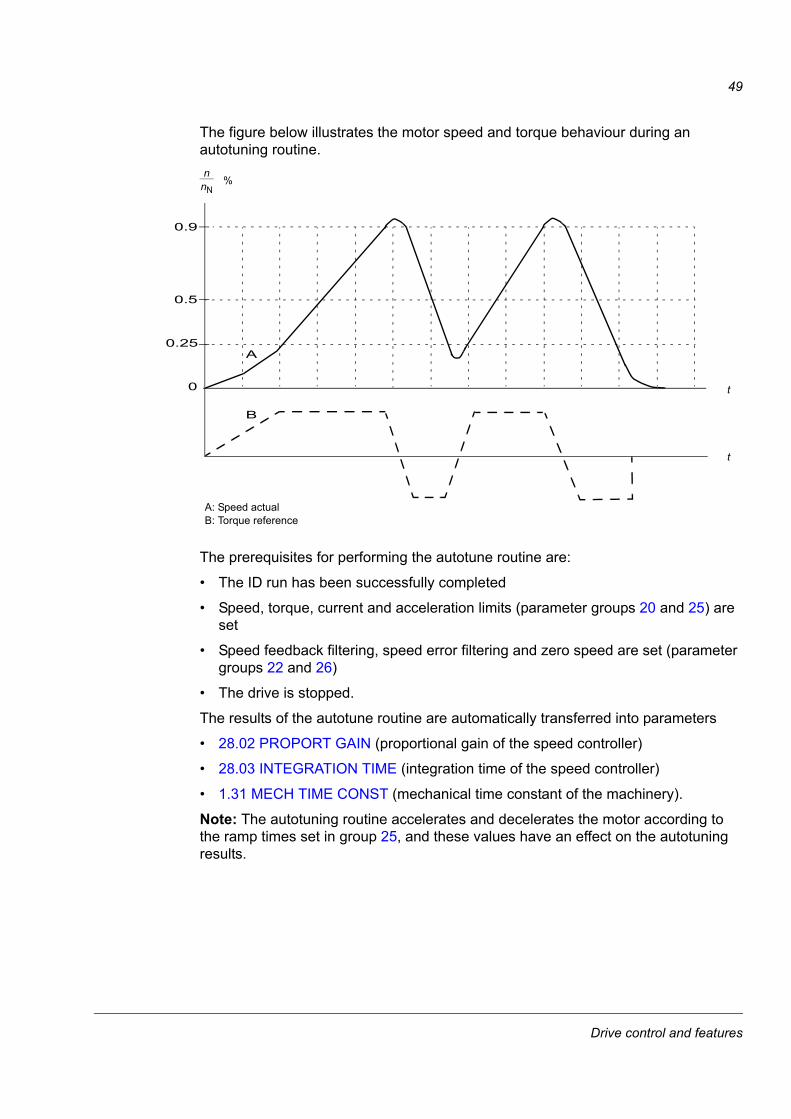
49
The figure below illustrates the motor speed and torque behaviour during an autotuning routine.
The prerequisites for performing the autotune routine are:
• The ID run has been successfully completed
• Speed, torque, current and acceleration limits (parameter groups 20 and 25) are set
• Speed feedback filtering, speed error filtering and zero speed are set (parameter groups 22 and 26)
• The drive is stopped.
The results of the autotune routine are automatically transferred into parameters
• 28.02 PROPORT GAIN (proportional gain of the speed controller)
• 28.03 INTEGRATION TIME (integration time of the speed controller)
• 1.31 MECH TIME CONST (mechanical time constant of the machinery).
Note: The autotuning routine accelerates and decelerates the motor according to the ramp times set in group 25, and these values have an effect on the autotuning results.
A: Speed actualB: Torque reference
%
t
n
B
nN
A
0
0.25
0.5
0.9
t
Drive control and features
50
The figure below shows speed responses at a speed reference step (typically 1…20%).
The figure below is a simplified block diagram of the speed controller. The controller output is the reference for the torque controller.
For more information on the use of the autotune function, see the description of parameter 28.16 PI TUNE MODE.
A: UndercompensatedB: Normally tuned (autotuning)C: Normally tuned (manually). Better dynamic performance than with BD: Overcompensated speed controller
%
t
n
CB D
nN
A
Derivative
Proportional,integral
Derivativeaccelerationcompensation
Torquereference
Speedreference
Actual speed
Errorvalue-
+ +++
Drive control and features

51
Motor feedback features
Motor encoder gear functionThe drive provides motor encoder gear function for compensating of mechanical gears between the motor shaft, the encoder and the load.
Motor encoder gear application example:
The motor encoder gear parameters 22.03 MOTOR GEAR MUL and 22.04 MOTOR GEAR DIV are set as follows:
Note: If the motor gear ratio differs from 1, the motor model uses an estimated speed instead of the speed feedback value.
M3~
Speed control uses the motor speed. If no encoder is mounted on the motor shaft, the motor encoder gear function must be applied in order to calculate the actual motor speed on the basis of the measured load speed.
ENCODERLOADGEARMOTOR
=22.03 MOTOR GEAR MUL22.04 MOTOR GEAR DIV
Actual speedEncoder 1/2 speed
Drive control and features
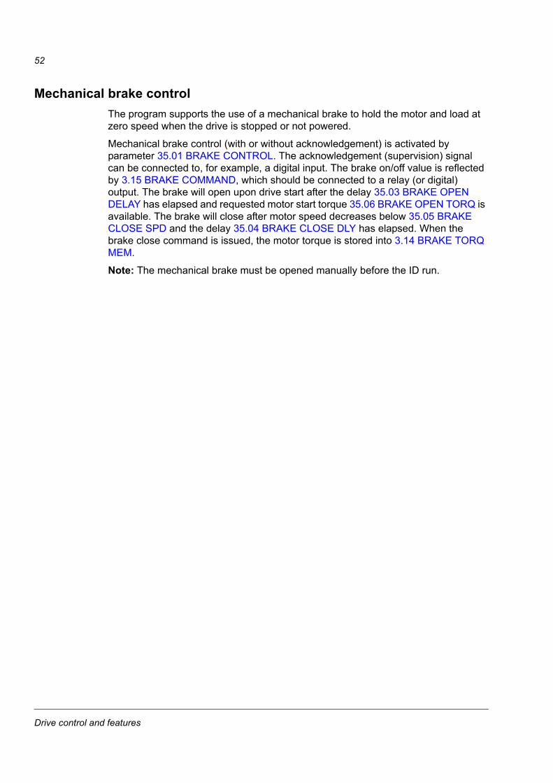
52
Mechanical brake controlThe program supports the use of a mechanical brake to hold the motor and load at zero speed when the drive is stopped or not powered.
Mechanical brake control (with or without acknowledgement) is activated by parameter 35.01 BRAKE CONTROL. The acknowledgement (supervision) signal can be connected to, for example, a digital input. The brake on/off value is reflected by 3.15 BRAKE COMMAND, which should be connected to a relay (or digital) output. The brake will open upon drive start after the delay 35.03 BRAKE OPEN DELAY has elapsed and requested motor start torque 35.06 BRAKE OPEN TORQ is available. The brake will close after motor speed decreases below 35.05 BRAKE CLOSE SPD and the delay 35.04 BRAKE CLOSE DLY has elapsed. When the brake close command is issued, the motor torque is stored into 3.14 BRAKE TORQ MEM.
Note: The mechanical brake must be opened manually before the ID run.
Drive control and features
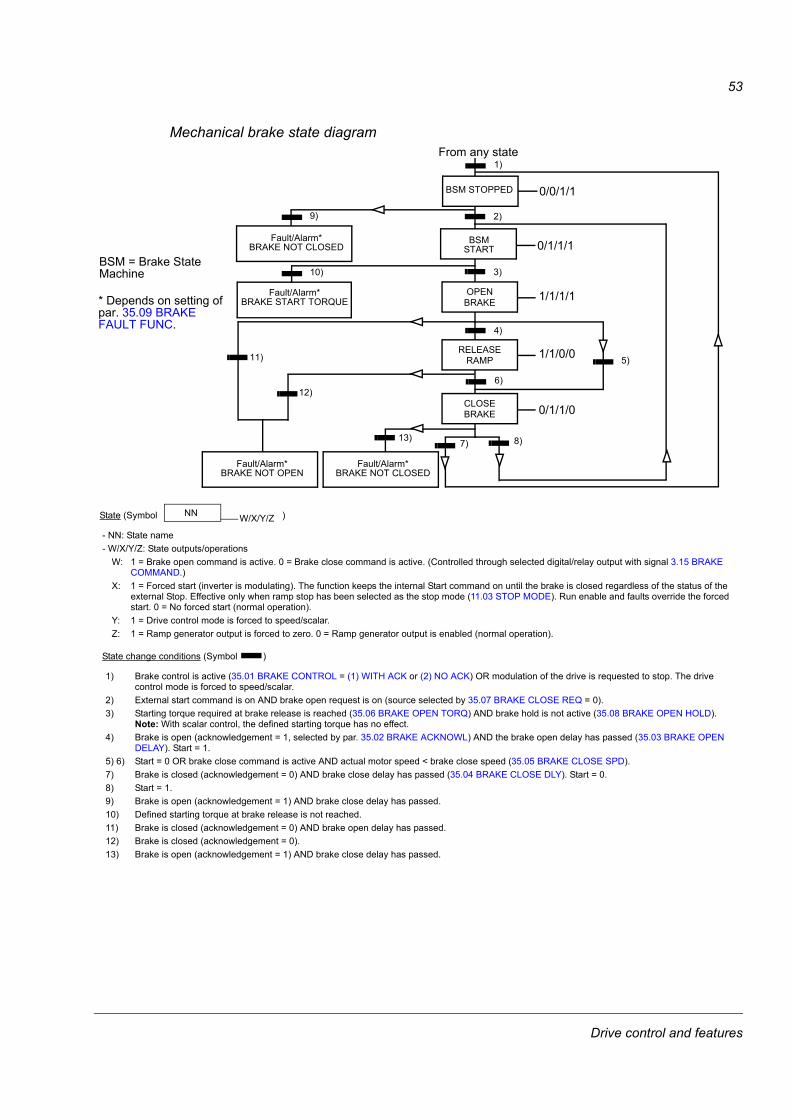
53
Mechanical brake state diagram
CLOSEBRAKE
From any state
0/1/1/0
1/1/1/1
1)
2)
3)
6)
7)
11)
12)
13)
5)
0/0/1/1
8)
State (Symbol )
- NN: State name- W/X/Y/Z: State outputs/operations
W: 1 = Brake open command is active. 0 = Brake close command is active. (Controlled through selected digital/relay output with signal 3.15 BRAKE COMMAND.)
X: 1 = Forced start (inverter is modulating). The function keeps the internal Start command on until the brake is closed regardless of the status of the external Stop. Effective only when ramp stop has been selected as the stop mode (11.03 STOP MODE). Run enable and faults override the forced start. 0 = No forced start (normal operation).
Y: 1 = Drive control mode is forced to speed/scalar.Z: 1 = Ramp generator output is forced to zero. 0 = Ramp generator output is enabled (normal operation).
NN W/X/Y/Z
State change conditions (Symbol )
1) Brake control is active (35.01 BRAKE CONTROL = (1) WITH ACK or (2) NO ACK) OR modulation of the drive is requested to stop. The drive control mode is forced to speed/scalar.
2) External start command is on AND brake open request is on (source selected by 35.07 BRAKE CLOSE REQ = 0).3) Starting torque required at brake release is reached (35.06 BRAKE OPEN TORQ) AND brake hold is not active (35.08 BRAKE OPEN HOLD).
Note: With scalar control, the defined starting torque has no effect. 4) Brake is open (acknowledgement = 1, selected by par. 35.02 BRAKE ACKNOWL) AND the brake open delay has passed (35.03 BRAKE OPEN
DELAY). Start = 1.5) 6) Start = 0 OR brake close command is active AND actual motor speed < brake close speed (35.05 BRAKE CLOSE SPD).7) Brake is closed (acknowledgement = 0) AND brake close delay has passed (35.04 BRAKE CLOSE DLY). Start = 0.8) Start = 1.9) Brake is open (acknowledgement = 1) AND brake close delay has passed. 10) Defined starting torque at brake release is not reached.11) Brake is closed (acknowledgement = 0) AND brake open delay has passed.12) Brake is closed (acknowledgement = 0).13) Brake is open (acknowledgement = 1) AND brake close delay has passed.
0/1/1/1Fault/Alarm*
BRAKE NOT CLOSED
9)
Fault/Alarm* BRAKE START TORQUE
10)
4)
BSM = Brake State Machine
* Depends on setting of par. 35.09 BRAKE FAULT FUNC.
BSM STOPPED
BSM START
1/1/0/0RELEASERAMP
OPENBRAKE
Fault/Alarm* BRAKE NOT CLOSED
Fault/Alarm* BRAKE NOT OPEN
Drive control and features
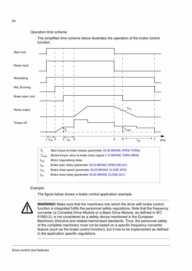
54
Operation time scheme
The simplified time scheme below illustrates the operation of the brake control function.
Example
The figure below shows a brake control application example.
WARNING! Make sure that the machinery into which the drive with brake control function is integrated fulfils the personnel safety regulations. Note that the frequency converter (a Complete Drive Module or a Basic Drive Module, as defined in IEC 61800-2), is not considered as a safety device mentioned in the European Machinery Directive and related harmonised standards. Thus, the personnel safety of the complete machinery must not be based on a specific frequency converter feature (such as the brake control function), but it has to be implemented as defined in the application specific regulations.
Ts Start torque at brake release (parameter 35.06 BRAKE OPEN TORQ)
Tmem Stored torque value at brake close (signal 3.14 BRAKE TORQ MEM)
tmd Motor magnetising delay
tod Brake open delay (parameter 35.03 BRAKE OPEN DELAY)
ncs Brake close speed (parameter 35.05 BRAKE CLOSE SPD)
tcd Brake close delay (parameter 35.04 BRAKE CLOSE DLY)
Start cmd
Modulating
Ref_Running
Brake open cmd
Ramp output
Torque ref
timetod tcd
ncs
Ts
Ramp input
tmd1 2 3 4 5 6 7
Tmem
Drive control and features
55
Motor
M
230 VAC
JCU unit
Mechanical brake
Brake control hardware
Emergency brake
X2
1 RO12 RO13 RO1
X3
11 DI5
13 +24 V
The brake on/off is controlled via signal 3.15 BRAKE COMMAND. The source for the brake supervision is selected by parameter 35.02 BRAKE ACKNOWL.The brake control hardware and wirings need to be done by the user.• Brake on/off control through selected relay/digital output.• Brake supervision through selected digital input.• Emergency brake switch in the brake control circuit.
• Brake on/off control through relay output (i.e. parameter 12.12 RO1 OUT PTR is set to P.03.15 = 3.15 BRAKE COMMAND).• Brake supervision through digital input DI5 (i.e. parameter 35.02 BRAKE ACKNOWL is set to P.02.01.04 = 2.01 DI STATUS bit 4)
Drive control and features

56
Emergency stopNote: The user is responsible for installing the emergency stop devices and all the additional devices needed for the emergency stop to fulfil the required emergency stop category classes.
The emergency stop signal is connected to the digital input which is selected as the source for the emergency stop activation (parameter 10.10 EM STOP OFF3 or 10.11 EM STOP OFF1). Emergency stop can also be activated through fieldbus (2.12 FBA MAIN CW).
Note: When an emergency stop signal is detected, the emergency stop function cannot be cancelled even though the signal is cancelled.
For more information, refer to Application Guide: Functional Safety Solutions with ACSM1 Drives (3AUA0000031517 [English]).
Miscellaneous features
Backup and restore of drive contentsGeneral
The drive offers a possibility of backing up numerous settings and configurations to external storage such as a PC file (using the DriveStudio tool) and the internal memory of the control panel. These settings and configurations can then be restored to the drive, or a number of drives.
Backup using DriveStudio includes
• Parameter settings
• User parameter sets
• Application program..
Backup using the drive control panel includes
• Parameter settings
• User parameter sets.
For detailed instructions for performing the backup/restore, refer to the DriveStudio and control panel documentation.
Limitations
A backup can be done without interfering with drive operation, but restoring a backup always resets and reboots the control unit, so restore is not possible with the drive running.
Backup/restore between different program variants (such as the Motion Control Program and the Speed and Torque Control Program) is not possible.
Restoring backup files from one firmware version to another is considered risky, so the results should be carefully observed and verified when done for the first time. The parameters and application support are bound to change between firmware versions and backups are not always compatible with other firmware versions even if
Drive control and features
57
restore is allowed by the backup/restore tool. Before using the backup/restore functions between different firmware versions, refer to the release notes of each version.
Applications should not be transferred between different firmware versions. Contact the supplier of the application when it needs to be updated for a new firmware version.
Parameter restore
Parameters are divided into three different groups that can be restored together or individually:
• Motor configuration parameters and identification (ID) run results
• Fieldbus adapter and encoder settings
• Other parameters.
For example, retaining the existing ID run results in the drive will make a new ID run unnecessary.
Restore of individual parameters can fail for the following reasons:
• The restored value does not fall within the minimum and maximum limits of the drive parameter
• The type of the restored parameter is different from that in the drive
• The restored parameter does not exist in the drive (often the case when restoring the parameters of a new firmware version to a drive with an older version)
• The backup does not contain a value for the drive parameter (often the case when restoring the parameters of an old firmware version to a drive with a newer version).
In these cases, the parameter is not restored; the backup/restore tool will warn the user and offer a possibility to set the parameter manually.
User parameter sets
The drive has four user parameter sets that can be saved to the permanent memory and recalled using drive parameters. It is also possible to use digital inputs to switch between different user parameter sets. See the descriptions of parameters 16.09…16.12.
A user parameter set contains all values of parameter groups 10 to 99 (except the fieldbus communication configuration settings).
As the motor settings are included in the user parameter sets, make sure the settings correspond to the motor used in the application before recalling a user set. In an application where different motors are used with one drive, the motor ID run needs to be performed with each motor and saved to different user sets. The appropriate set can then be recalled when the motor is switched.
Drive control and features

58
Drive-to-drive linkThe drive-to-drive link is a daisy-chained RS-485 transmission line that allows basic master/follower communication with one master drive and multiple followers. For more information, see Appendix B – Drive-to-drive link.
Drive control and features
59
Default connections of the control unit
What this chapter containsThis chapter shows the default control connections of the JCU Control Unit.
More information on the connectivity of the JCU is given in the Hardware Manual of the drive.
Default connections of the control unit

60
Notes:*Total maximum current: 200 mA
1) Selected by par. 12.01 DIO1 CONF.2) Selected by par. 12.02 DIO2 CONF.3) Selected by par. 12.03 DIO3 CONF.4) Selected by jumper J1.5) Selected by jumper J2.
X1External power input24 V DC, 1.6 A
+24VI 1GND 2
X2Relay output: Brake close/open250 V AC / 30 V DC2 A
NO 1COM 2NC 3
X3+24 V DC* +24VD 1Digital I/O ground DGND 2Digital input 1: Stop/start (par. 10.02 and 10.05) DI1 3Digital input 2: EXT1/EXT2 (par. 34.01) DI2 4+24 V DC* +24VD 5Digital I/O ground DGND 6Digital input 3: Fault reset (par. 10.08) DI3 7Digital input 4: Not connected DI4 8+24 V DC* +24VD 9Digital I/O ground DGND 10Digital input 5: Not connected DI5 11Digital input 6: Not connected DI6 12+24 V DC* +24VD 13Digital I/O ground DGND 14Digital input/output 1 1): Ready DIO1 15Digital input/output 2 2): Running DIO2 16+24 V DC* +24VD 17Digital I/O ground DGND 18Digital input/output 3 3): Fault DIO3 19
X4Reference voltage (+) +VREF 1Reference voltage (–) –VREF 2Ground AGND 3Analogue input 1 (mA or V) 4): Speed reference (par. 24.01)
AI1+ 4AI1– 5
Analogue input 2 (mA or V) 5): Torque reference (par. 32.01)
AI2+ 6AI2– 7
AI1 current/voltage selection J1AI2 current/voltage selection J2Thermistor input TH 8Ground AGND 9Analogue output 1 (mA): Output current AO1 (I) 10Analogue output 2 (V): Actual speed AO2 (U) 11Ground AGND 12
X5Drive-to-drive link termination J3
Drive-to-drive linkB 1A 2
BGND 3X6
Safe Torque Off. Both circuits must be closed for the drive to start. See the appropriate drive hardware manual.
OUT1 1OUT2 2
IN1 3IN2 4
Control panel connectionMemory unit connection
Current:
Voltage:
J1/2
J1/2
AIx
AIx
Default connections of the control unit

61
Parameters and firmware blocks
What this chapter containsThis chapter lists and describes the parameters provided by the firmware.
Types of parametersParameters are user-adjustable operation instructions of the drive (groups 10…99). There are four basic types of parameters: Actual signals, value parameters, value pointer parameters and bit pointer parameters.
Actual signal
Type of parameter that is the result of a measurement or calculation by the drive. Actual signals can be monitored, but not adjusted, by the user. Actual signals are typically contained within parameter groups 1…9.
For additional actual signal data, e.g. update cycles and fieldbus equivalents, see chapter Parameter data.
Value parameter
A value parameter has a fixed set of choices or a setting range.
Example 1: Motor phase loss supervision is activated by selecting (1) Fault from the selection list of parameter 46.04 MOT PHASE LOSS.
Example 2: The motor nominal power (kW) is set by writing the appropriate value to parameter 99.10 MOT NOM POWER, e.g. 10.
Value pointer parameter
A value pointer parameter points to the value of another parameter. The source parameter is given in format P.xx.yy, where xx = Parameter group; yy = Parameter index. In addition, value pointer parameters may have a set of pre-selected choices.
Example: Motor current signal, 1.05 CURRENT PERC, is connected to analogue output AO1 by setting parameter 15.01 AO1 PTR to value P.01.05.
Bit pointer parameter
A bit pointer parameter points to the value of a bit in another parameter, or can be fixed to 0 (FALSE) or 1 (TRUE). In addition, bit pointer parameters may have a set of pre-selected choices.
When adjusting a bit pointer parameter on the optional control panel, CONST is selected in order to fix the value to 0 (displayed as “C.FALSE”) or 1 (“C.TRUE”). POINTER is selected to define a source from another parameter.
A pointer value is given in format P.xx.yy.zz, where xx = Parameter group, yy = Parameter index, zz = Bit number.
Example: Digital input DI5 status, 2.01 DI STATUS bit 4, is used for brake supervision by setting parameter 35.02 BRAKE ACKNOWL to value P.02.01.04.
Parameters and firmware blocks
62
Note: Pointing to a nonexisting bit will be interpreted as 0 (FALSE).
For additional parameter data, e.g. update cycles and fieldbus equivalents, see chapter Parameter data.
Firmware blocksFirmware blocks accessible from the DriveSPC PC tool are described in the parameter group that contains the most of the block inputs/outputs. Whenever a block has inputs or outputs outside the current parameter group, a reference is given. Likewise, parameters have a reference to the firmware block they are included in (if any).
Note: Not all parameters are available through firmware blocks.
��������� �(
����������� ���
-��(�������������,��#�����������*�.�����
-��(���������#���,��#������#���#� ����(�.�!���
-��(�!�������#������#�������#����"�����.�����
-��(�����������������#�������������/�����.�����
����(��������������������������
����(�(��������##���� ��������������
����(�*�������/�,�"/�������������
����(�+������" ����#�� ��������������
����(�0������" ����� ��������������
!��������#���%���
!�(��������##"#�����
!�*������" ���"#1
1 Inputs
2 Outputs
3 Input parameter values
4 Pointer parameter indicator “<“
5 Parameter 26.01 is set to value P.1.1, i.e. parameter 1.01 SPEED ACT. The “7” means the parameter can be found on page 7 of DriveSPC.
6 Information of the block internal execution order (“TLF4”) and time level (“250 µsec”). Time level, i.e. update cycle, is application-specific. See the time level of the block in DriveSPC.
7 Firmware block ID number in the application program
8 Firmware block execution order for the selected update cycle ID
2
3
6
7
8
4
5
1
Parameters and firmware blocks
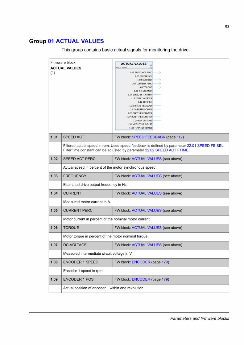
63
Group 01 ACTUAL VALUESThis group contains basic actual signals for monitoring the drive.
01Firmware block:ACTUAL VALUES(1)
1.01 SPEED ACT FW block: SPEED FEEDBACK (page 112)
Filtered actual speed in rpm. Used speed feedback is defined by parameter 22.01 SPEED FB SEL. Filter time constant can be adjusted by parameter 22.02 SPEED ACT FTIME.
1.02 SPEED ACT PERC FW block: ACTUAL VALUES (see above)
Actual speed in percent of the motor synchronous speed.
1.03 FREQUENCY FW block: ACTUAL VALUES (see above)
Estimated drive output frequency in Hz.
1.04 CURRENT FW block: ACTUAL VALUES (see above)
Measured motor current in A.
1.05 CURRENT PERC FW block: ACTUAL VALUES (see above)
Motor current in percent of the nominal motor current.
1.06 TORQUE FW block: ACTUAL VALUES (see above)
Motor torque in percent of the motor nominal torque.
1.07 DC-VOLTAGE FW block: ACTUAL VALUES (see above)
Measured intermediate circuit voltage in V.
1.08 ENCODER 1 SPEED FW block: ENCODER (page 179)
Encoder 1 speed in rpm.
1.09 ENCODER 1 POS FW block: ENCODER (page 179)
Actual position of encoder 1 within one revolution.
ACTUAL VALUES 14
MISC_3 2 msec (1)
1.02 SPEED ACT PERC
1.03 FREQUENCY
1.04 CURRENT
1.05 CURRENT PERC
1.06 TORQUE
1.07 DC-VOLTAGE
1.14 SPEED ESTIMATED
1.15 TEMP INVERTER
1.16 TEMP BC
1.20 BRAKE RES LOAD
1.22 INVERTER POWER
1.26 ON TIME COUNTER
1.27 RUN TIME COUNTER
1.28 FAN ON-TIME
1.31 MECH TIME CONST
1.38 TEMP INT BOARD
Parameters and firmware blocks

64
1.10 ENCODER 2 SPEED FW block: ENCODER (page 179)
Encoder 2 speed in rpm.
1.11 ENCODER 2 POS FW block: ENCODER (page 179)
Actual position of encoder 2 within one revolution.
Firmware block:POS FEEDBACK(60)
1.12 POS ACT FW block: POS FEEDBACK (see above)
Actual position of the encoder.
1.13 POS 2ND ENC FW block: POS FEEDBACK (see above)
Scaled actual position of encoder 2 in revolutions.
1.14 SPEED ESTIMATED FW block: ACTUAL VALUES (see above)
Estimated motor speed in rpm.
1.15 TEMP INVERTER FW block: ACTUAL VALUES (see above)
Measured temperature of the heatsink in Celsius.
1.16 TEMP BC FW block: ACTUAL VALUES (see above)
Brake chopper IGBT temperature in Celsius.
1.17 MOTOR TEMP FW block: MOT THERM PROT (page 153)
Measured motor temperature in Celsius when a KTY sensor is used. (With a PTC sensor, the value is always 0.)
1.18 MOTOR TEMP EST FW block: MOT THERM PROT (page 153)
Estimated motor temperature in Celsius.
1.19 USED SUPPLY VOLT FW block: VOLTAGE CTRL (page 161)
Either the user-given supply voltage (parameter 47.04 SUPPLY VOLTAGE), or, if auto-identification is enabled by parameter 47.03 SUPPLVOLTAUTO-ID, the automatically determined supply voltage.
1.20 BRAKE RES LOAD FW block: ACTUAL VALUES (see above)
Estimated temperature of the braking resistor. The value is given in percent of the temperature the resistor reaches when loaded with the power defined by parameter 48.04 BR POWER MAX CNT.
1.21 CPU USAGE FW block: None
Microprocessor load in percent.
POS FEEDBACK 36
POSCTR 500 μsec (1)
1.12 POS ACT
1.13 POS 2ND ENC
Parameters and firmware blocks

65
1.22 INVERTER POWER FW block: ACTUAL VALUES (see above)
Drive output power in kilowatts.
1.26 ON TIME COUNTER FW block: ACTUAL VALUES (see above)
This counter runs when the drive is powered. The counter can be reset using the DriveStudio tool.
1.27 RUN TIME COUNTER FW block: ACTUAL VALUES (see above)
Motor run time counter. The counter run when the drive modulates. The counter can be reset using the DriveStudio tool.
1.28 FAN ON-TIME FW block: ACTUAL VALUES (see above)
Running time of the drive cooling fan. Can be reset by entering 0.
1.31 MECH TIME CONST FW block: ACTUAL VALUES (see above)
Mechanical time constant of the drive and the machinery as determined by the speed controller autotune function. See parameter 28.16 PI TUNE MODE on page 135.
1.38 TEMP INT BOARD FW block: ACTUAL VALUES (see above)
Measured temperature of the interface board in degrees Celsius.
Parameters and firmware blocks

66
Group 02 I/O VALUESThis group contains information on the I/Os of the drive.
022.01 DI STATUS FW block: DI (page 95)
Status word of the digital inputs. Example: 000001 = DI1 is on, DI2 to DI6 are off.
2.02 RO STATUS FW block: RO (page 95)
Status of relay output. 1 = RO is energized.
2.03 DIO STATUS FW blocks: DIO1 (page 93), DIO2 (page 93), DIO3 (page 93)
Status word of digital inputs/outputs DIO1…3. Example: 001 = DIO1 is on, DIO2 and DIO3 are off.
2.04 AI1 FW block: AI1 (page 97)
Analogue input AI1 value in V or mA. The type is selected with jumper J1 on the JCU Control Unit.
2.05 AI1 SCALED FW block: AI1 (page 97)
Scaled value of analogue input AI1. See parameters 13.04 AI1 MAX SCALE and 13.05 AI1 MIN SCALE.
2.06 AI2 FW block: AI2 (page 98)
Analogue input AI2 value in V or mA. The type is selected with jumper J2 on the JCU Control Unit.
2.07 AI2 SCALED FW block: AI2 (page 98)
Scaled value of analogue input AI2. See parameters 13.09 AI2 MAX SCALE and 13.10 AI2 MIN SCALE.
2.08 AO1 FW block: AO1 (page 101)
Analogue output AO1 value in mA
2.09 AO2 FW block: AO2 (page 102)
Analogue output AO2 value in V
2.10 DIO2 FREQ IN FW block: DIO2 (page 93)
Scaled value of DIO2 when it is used as a frequency input. See parameters 12.02 DIO2 CONF and 12.14 DIO2 F MAX…12.17 DIO2 F MIN SCALE.
2.11 DIO3 FREQ OUT FW block: DIO3 (page 93)
Frequency output value of DIO3 when it is used as a frequency output. See parameters 12.03 DIO3 CONF and 12.08 DIO3 F MAX…12.11 DIO3 F MIN SCALE.
Parameters and firmware blocks

67
2.12 FBA MAIN CW FW block: FIELDBUS (page 165)
Control Word for fieldbus communication.Log. = Logical combination (i.e. Bit AND/OR Selection parameter). Par. = Selection parameter. See State diagram on page 342.
Bit Name Val. Information Log. Par.0 STOP* 1 Stop according to the stop mode selected by 11.03
STOP MODE or according to the requested stop mode (bits 2…6). Note: Simultaneous STOP and START commands result in a stop command.
OR 10.02,10.03,10.05,10.06
0 No operation1 START 1 Start. Note: Simultaneous STOP and START
commands result in a stop command.OR 10.02,
10.03,10.05,10.06
0 No operation
2 STPMODE EM OFF*
1 Emergency OFF2 (bit 0 must be 1): Drive is stopped by cutting off the motor power supply (the inverter IGBTs are blocked). The motor coasts to stop. The drive will restart only with the next rising edge of the start signal when the run enable signal is on.
AND -
0 No operation3 STPMODE
EM STOP*1 Emergency stop OFF3 (bit 0 must be 1): Stop within
the time defined by 25.11 EM STOP TIME.AND 10.10
0 No operation4 STPMODE
OFF1*1 Emergency stop OFF1 (bit 0 must be 1): Stop along
the currently active deceleration ramp.AND 10.11
0 No operation5 STPMODE
RAMP*1 Stop along the currently active deceleration ramp. - 11.030 No operation
6 STPMODE COAST*
1 Coast to stop. - 11.030 No operation
7 RUNENABLE
1 Activate run enable. AND 10.090 Activate run disable.
8 RESET 0->1 Fault reset if an active fault exists. OR 10.08other No operation
9 JOGGING 1 1 Activate jogging function 1. See section Jogging on page 47.
OR 10.07
0 Jogging function 1 disabled* If all stop mode bits 2…6 are 0, stop mode is selected by 11.03 STOP MODE. Coast stop (bit 6) overrides the emergency stop (bit 2/3/4). Emergency stop overrides the normal ramp stop (bit 5).
Parameters and firmware blocks
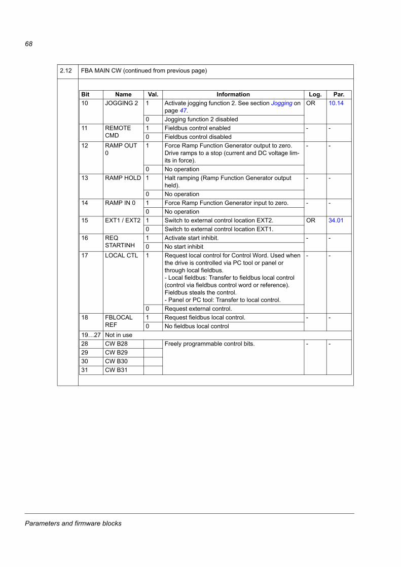
68
2.12 FBA MAIN CW (continued from previous page)
Bit Name Val. Information Log. Par.10 JOGGING 2 1 Activate jogging function 2. See section Jogging on
page 47.OR 10.14
0 Jogging function 2 disabled11 REMOTE
CMD1 Fieldbus control enabled - -0 Fieldbus control disabled
12 RAMP OUT 0
1 Force Ramp Function Generator output to zero. Drive ramps to a stop (current and DC voltage lim-its in force).
- -
0 No operation13 RAMP HOLD 1 Halt ramping (Ramp Function Generator output
held).- -
0 No operation14 RAMP IN 0 1 Force Ramp Function Generator input to zero. - -
0 No operation15 EXT1 / EXT2 1 Switch to external control location EXT2. OR 34.01
0 Switch to external control location EXT1.16 REQ
STARTINH1 Activate start inhibit. - -0 No start inhibit
17 LOCAL CTL 1 Request local control for Control Word. Used when the drive is controlled via PC tool or panel or through local fieldbus.- Local fieldbus: Transfer to fieldbus local control (control via fieldbus control word or reference). Fieldbus steals the control.- Panel or PC tool: Transfer to local control.
- -
0 Request external control.18 FBLOCAL
REF1 Request fieldbus local control. - -0 No fieldbus local control
19…27 Not in use28 CW B28 Freely programmable control bits. - -29 CW B2930 CW B3031 CW B31
Parameters and firmware blocks

69
2.13 FBA MAIN SW FW block: FIELDBUS (page 165)
Status Word for fieldbus communication. See State diagram on page 342.
Bit Name Value Information0 READY 1 Drive is ready to receive start command.
0 Drive is not ready.1 ENABLED 1 External run enable signal is received.
0 No external run enable signal is received.2 RUNNING 1 Drive is modulating.
0 Drive is not modulating.3 REF RUNNING 1 Normal operation is enabled. Drive is running and following given
reference.0 Normal operation is disabled. Drive is not following given reference
(for example, modulating during magnetization).4 EM OFF
(OFF2)1 Emergency OFF2 is active.0 Emergency OFF2 is inactive.
5 EM STOP (OFF3)
1 Emergency stop OFF3 (ramp stop) is active.0 Emergency OFF3 is inactive.
6 ACK STARTINH
1 Start inhibit is active.0 Start inhibit is inactive.
7 ALARM 1 An alarm is active. See chapter Fault tracing.0 No alarm is active.
8 AT SETPOINT 1 Drive is at setpoint. Actual value equals reference value (i.e. the difference between the actual speed and the speed reference is within the speed window defined by 26.07 SPEED WINDOW).
0 Drive has not reached setpoint.9 LIMIT 1 Operation is limited by any torque or current limit.
0 Operation is within torque/current limits.10 ABOVE LIMIT 1 Actual speed exceeds the defined limit, 22.07 ABOVE SPEED LIM.
0 Actual speed is within the defined limits.11 EXT2 ACT 1 External control location EXT2 is active.
0 External control location EXT1 is active.12 LOCAL FB 1 Fieldbus local control is active.
0 Fieldbus local control is inactive.13 ZERO SPEED 1 Drive speed is below limit set by par. 22.05 ZERO SPEED LIMIT.
0 Drive has not reached zero speed limit.14 REV ACT 1 Drive is running in reverse direction.
0 Drive is running in forward direction.15 Not in use16 FAULT 1 Fault is active. See chapter Fault tracing.
0 No fault is active.17 LOCAL PANEL 1 Local control is active, i.e. drive is controlled from PC tool or control
panel.0 Local control is inactive.
Parameters and firmware blocks

70
2.13 FBA MAIN SW (continued from previous page)
2.14 FBA MAIN REF1 FW block: FIELDBUS (page 165)
Scaled fieldbus reference 1. See parameter 50.04 FBA REF1 MODESEL.
2.15 FBA MAIN REF2 FW block: FIELDBUS (page 165)
Scaled fieldbus reference 2. See parameter 50.05 FBA REF2 MODESEL.
2.16 FEN DI STATUS FW block: ENCODER (page 179)
Status of digital inputs of FEN-xx encoder interfaces in drive option Slots 1 and 2. Examples:000001 (01h) = DI1 of FEN-xx in Slot 1 is ON, all others are OFF.000010 (02h) = DI2 of FEN-xx in Slot 1 is ON, all others are OFF.010000 (10h) = DI1 of FEN-xx in Slot 2 is ON, all others are OFF.100000 (20h) = DI2 of FEN-xx in Slot 2 is ON, all others are OFF.
2.17 D2D MAIN CW FW block: D2D COMMUNICATION (page 174)
Drive-to-drive control word received through the drive-to-drive link. See also actual signal 2.18 below.
Bit Name Value Information18…26 Not in use with Speed and Torque Control Program27 REQUEST CTL 1 Control word is requested from fieldbus.
0 Control word is not requested from fieldbus.28 SW B28 Programmable status bits (unless fixed by the used
profile). See parameters 50.08…50.11 and the user manual of the fieldbus adapter.
29 SW B2930 SW B3031 SW B31
Bit Information0 Stop.1 Start.
2…6 Reserved.7 Run enable. By default, not connected in a follower drive.8 Reset. By default, not connected in a follower drive.
9…14 Freely assignable through bit pointer parameters.15 EXT1/EXT2 selection. 0 = EXT1 active, 1 = EXT2 active. By default, not connected in a
follower drive.
Parameters and firmware blocks

71
2.18 D2D FOLLOWER CW FW block: DRIVE LOGIC (page 84)
Drive-to-drive control word sent to the followers by default. See also firmware block D2D COMMUNICATION on page 174.
2.19 D2D REF1 FW block: D2D COMMUNICATION (page 174)
Drive-to-drive reference 1 received through the drive-to-drive link.
2.20 D2D REF2 FW block: D2D COMMUNICATION (page 174)
Drive-to-drive reference 2 received through the drive-to-drive link.
Bit Information0 Stop.1 Start.
2…6 Reserved.7 Run enable.8 Reset.
9…14 Reserved.15 EXT1/EXT2 selection. 0 = EXT1 active, 1 = EXT2 active.
Parameters and firmware blocks
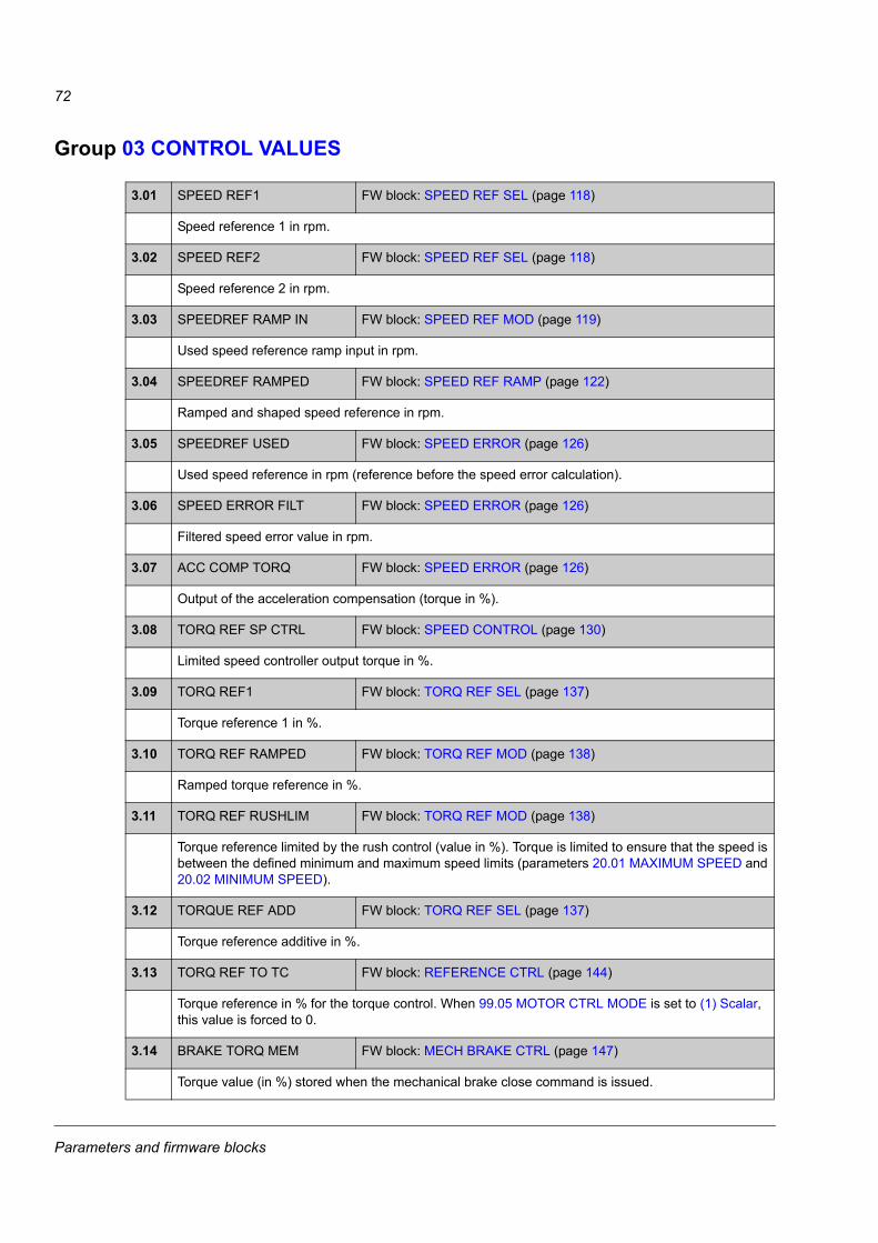
72
Group 03 CONTROL VALUES033.01 SPEED REF1 FW block: SPEED REF SEL (page 118)
Speed reference 1 in rpm.
3.02 SPEED REF2 FW block: SPEED REF SEL (page 118)
Speed reference 2 in rpm.
3.03 SPEEDREF RAMP IN FW block: SPEED REF MOD (page 119)
Used speed reference ramp input in rpm.
3.04 SPEEDREF RAMPED FW block: SPEED REF RAMP (page 122)
Ramped and shaped speed reference in rpm.
3.05 SPEEDREF USED FW block: SPEED ERROR (page 126)
Used speed reference in rpm (reference before the speed error calculation).
3.06 SPEED ERROR FILT FW block: SPEED ERROR (page 126)
Filtered speed error value in rpm.
3.07 ACC COMP TORQ FW block: SPEED ERROR (page 126)
Output of the acceleration compensation (torque in %).
3.08 TORQ REF SP CTRL FW block: SPEED CONTROL (page 130)
Limited speed controller output torque in %.
3.09 TORQ REF1 FW block: TORQ REF SEL (page 137)
Torque reference 1 in %.
3.10 TORQ REF RAMPED FW block: TORQ REF MOD (page 138)
Ramped torque reference in %.
3.11 TORQ REF RUSHLIM FW block: TORQ REF MOD (page 138)
Torque reference limited by the rush control (value in %). Torque is limited to ensure that the speed is between the defined minimum and maximum speed limits (parameters 20.01 MAXIMUM SPEED and 20.02 MINIMUM SPEED).
3.12 TORQUE REF ADD FW block: TORQ REF SEL (page 137)
Torque reference additive in %.
3.13 TORQ REF TO TC FW block: REFERENCE CTRL (page 144)
Torque reference in % for the torque control. When 99.05 MOTOR CTRL MODE is set to (1) Scalar, this value is forced to 0.
3.14 BRAKE TORQ MEM FW block: MECH BRAKE CTRL (page 147)
Torque value (in %) stored when the mechanical brake close command is issued.
Parameters and firmware blocks
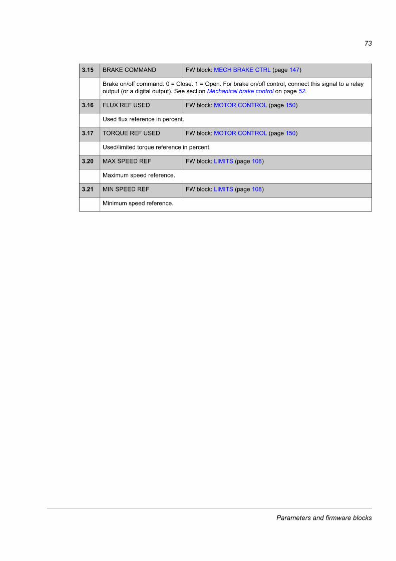
73
3.15 BRAKE COMMAND FW block: MECH BRAKE CTRL (page 147)
Brake on/off command. 0 = Close. 1 = Open. For brake on/off control, connect this signal to a relay output (or a digital output). See section Mechanical brake control on page 52.
3.16 FLUX REF USED FW block: MOTOR CONTROL (page 150)
Used flux reference in percent.
3.17 TORQUE REF USED FW block: MOTOR CONTROL (page 150)
Used/limited torque reference in percent.
3.20 MAX SPEED REF FW block: LIMITS (page 108)
Maximum speed reference.
3.21 MIN SPEED REF FW block: LIMITS (page 108)
Minimum speed reference.
Parameters and firmware blocks

74
Group 06 DRIVE STATUS066.01 STATUS WORD 1 FW block: DRIVE LOGIC (page 84)
Status word 1.
Bit Name Val. Information0 READY 1 Drive is ready to receive start command.
0 Drive is not ready.1 ENABLED 1 External run enable signal is received.
0 No external run enable signal is received.2 STARTED 1 Drive has received start command.
0 Drive has not received start command.3 RUNNING 1 Drive is modulating.
0 Drive is not modulating.4 EM OFF (OFF2) 1 Emergency OFF2 is active.
0 Emergency OFF2 is inactive.5 EM STOP
(OFF3)1 Emergency stop OFF3 (ramp stop) is active.0 Emergency OFF3 is inactive.
6 ACK STARTINH 1 Start inhibit is active.0 Start inhibit is inactive.
7 ALARM 1 An alarm is active. See chapter Fault tracing.0 No alarm
8 EXT2 ACT 1 External control EXT2 is active.0 External control EXT1 is active.
9 LOCAL FB 1 Fieldbus local control is active.0 Fieldbus local control is inactive.
10 FAULT 1 A fault is active. See chapter Fault tracing.0 No fault
11 LOCAL PANEL 1 Local control is active, i.e. drive is controlled from PC tool or control panel.
0 Local control is inactive.12 NOT FAULTED 1 No fault
0 A fault is active. See chapter Fault tracing.13…15 Reserved
Parameters and firmware blocks
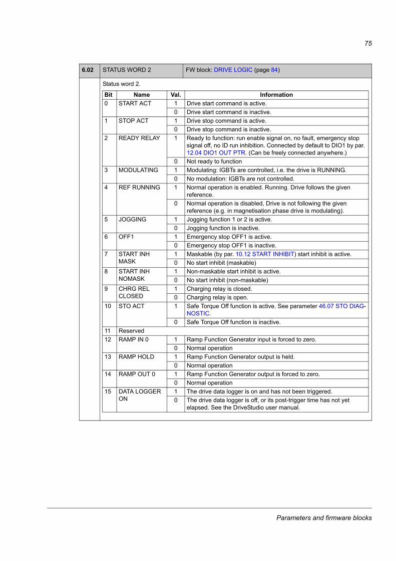
75
6.02 STATUS WORD 2 FW block: DRIVE LOGIC (page 84)
Status word 2.
Bit Name Val. Information0 START ACT 1 Drive start command is active.
0 Drive start command is inactive.1 STOP ACT 1 Drive stop command is active.
0 Drive stop command is inactive.2 READY RELAY 1 Ready to function: run enable signal on, no fault, emergency stop
signal off, no ID run inhibition. Connected by default to DIO1 by par. 12.04 DIO1 OUT PTR. (Can be freely connected anywhere.)
0 Not ready to function3 MODULATING 1 Modulating: IGBTs are controlled, i.e. the drive is RUNNING.
0 No modulation: IGBTs are not controlled.4 REF RUNNING 1 Normal operation is enabled. Running. Drive follows the given
reference.0 Normal operation is disabled, Drive is not following the given
reference (e.g. in magnetisation phase drive is modulating).5 JOGGING 1 Jogging function 1 or 2 is active.
0 Jogging function is inactive.6 OFF1 1 Emergency stop OFF1 is active.
0 Emergency stop OFF1 is inactive.7 START INH
MASK1 Maskable (by par. 10.12 START INHIBIT) start inhibit is active.0 No start inhibit (maskable)
8 START INH NOMASK
1 Non-maskable start inhibit is active.0 No start inhibit (non-maskable)
9 CHRG REL CLOSED
1 Charging relay is closed.0 Charging relay is open.
10 STO ACT 1 Safe Torque Off function is active. See parameter 46.07 STO DIAG-NOSTIC.
0 Safe Torque Off function is inactive.11 Reserved12 RAMP IN 0 1 Ramp Function Generator input is forced to zero.
0 Normal operation13 RAMP HOLD 1 Ramp Function Generator output is held.
0 Normal operation14 RAMP OUT 0 1 Ramp Function Generator output is forced to zero.
0 Normal operation15 DATA LOGGER
ON1 The drive data logger is on and has not been triggered.0 The drive data logger is off, or its post-trigger time has not yet
elapsed. See the DriveStudio user manual.
Parameters and firmware blocks
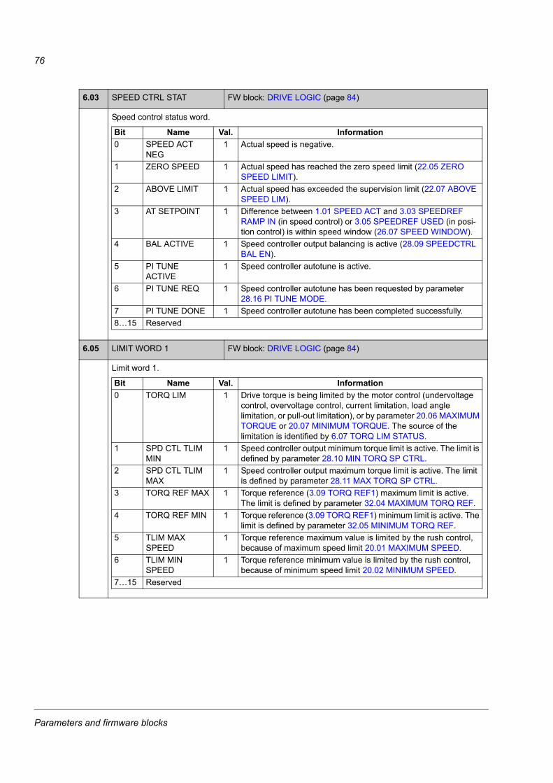
76
6.03 SPEED CTRL STAT FW block: DRIVE LOGIC (page 84)
Speed control status word.
6.05 LIMIT WORD 1 FW block: DRIVE LOGIC (page 84)
Limit word 1.
Bit Name Val. Information0 SPEED ACT
NEG1 Actual speed is negative.
1 ZERO SPEED 1 Actual speed has reached the zero speed limit (22.05 ZERO SPEED LIMIT).
2 ABOVE LIMIT 1 Actual speed has exceeded the supervision limit (22.07 ABOVE SPEED LIM).
3 AT SETPOINT 1 Difference between 1.01 SPEED ACT and 3.03 SPEEDREF RAMP IN (in speed control) or 3.05 SPEEDREF USED (in posi-tion control) is within speed window (26.07 SPEED WINDOW).
4 BAL ACTIVE 1 Speed controller output balancing is active (28.09 SPEEDCTRL BAL EN).
5 PI TUNE ACTIVE
1 Speed controller autotune is active.
6 PI TUNE REQ 1 Speed controller autotune has been requested by parameter 28.16 PI TUNE MODE.
7 PI TUNE DONE 1 Speed controller autotune has been completed successfully.8…15 Reserved
Bit Name Val. Information0 TORQ LIM 1 Drive torque is being limited by the motor control (undervoltage
control, overvoltage control, current limitation, load angle limitation, or pull-out limitation), or by parameter 20.06 MAXIMUM TORQUE or 20.07 MINIMUM TORQUE. The source of the limitation is identified by 6.07 TORQ LIM STATUS.
1 SPD CTL TLIM MIN
1 Speed controller output minimum torque limit is active. The limit is defined by parameter 28.10 MIN TORQ SP CTRL.
2 SPD CTL TLIM MAX
1 Speed controller output maximum torque limit is active. The limit is defined by parameter 28.11 MAX TORQ SP CTRL.
3 TORQ REF MAX 1 Torque reference (3.09 TORQ REF1) maximum limit is active. The limit is defined by parameter 32.04 MAXIMUM TORQ REF.
4 TORQ REF MIN 1 Torque reference (3.09 TORQ REF1) minimum limit is active. The limit is defined by parameter 32.05 MINIMUM TORQ REF.
5 TLIM MAX SPEED
1 Torque reference maximum value is limited by the rush control, because of maximum speed limit 20.01 MAXIMUM SPEED.
6 TLIM MIN SPEED
1 Torque reference minimum value is limited by the rush control, because of minimum speed limit 20.02 MINIMUM SPEED.
7…15 Reserved
Parameters and firmware blocks
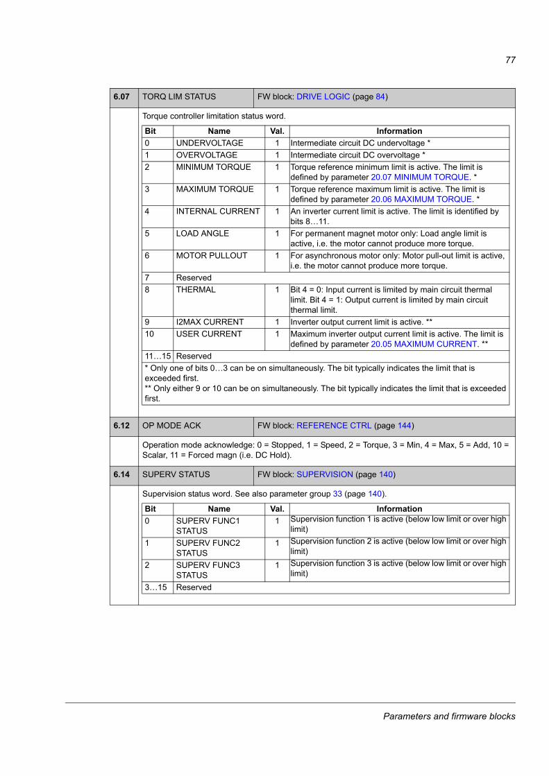
77
6.07 TORQ LIM STATUS FW block: DRIVE LOGIC (page 84)
Torque controller limitation status word.
6.12 OP MODE ACK FW block: REFERENCE CTRL (page 144)
Operation mode acknowledge: 0 = Stopped, 1 = Speed, 2 = Torque, 3 = Min, 4 = Max, 5 = Add, 10 = Scalar, 11 = Forced magn (i.e. DC Hold).
6.14 SUPERV STATUS FW block: SUPERVISION (page 140)
Supervision status word. See also parameter group 33 (page 140).
Bit Name Val. Information0 UNDERVOLTAGE 1 Intermediate circuit DC undervoltage *1 OVERVOLTAGE 1 Intermediate circuit DC overvoltage *2 MINIMUM TORQUE 1 Torque reference minimum limit is active. The limit is
defined by parameter 20.07 MINIMUM TORQUE. *3 MAXIMUM TORQUE 1 Torque reference maximum limit is active. The limit is
defined by parameter 20.06 MAXIMUM TORQUE. *4 INTERNAL CURRENT 1 An inverter current limit is active. The limit is identified by
bits 8…11.5 LOAD ANGLE 1 For permanent magnet motor only: Load angle limit is
active, i.e. the motor cannot produce more torque.6 MOTOR PULLOUT 1 For asynchronous motor only: Motor pull-out limit is active,
i.e. the motor cannot produce more torque.7 Reserved8 THERMAL 1 Bit 4 = 0: Input current is limited by main circuit thermal
limit. Bit 4 = 1: Output current is limited by main circuit thermal limit.
9 I2MAX CURRENT 1 Inverter output current limit is active. **10 USER CURRENT 1 Maximum inverter output current limit is active. The limit is
defined by parameter 20.05 MAXIMUM CURRENT. **11…15 Reserved* Only one of bits 0…3 can be on simultaneously. The bit typically indicates the limit that is exceeded first.** Only either 9 or 10 can be on simultaneously. The bit typically indicates the limit that is exceeded first.
Bit Name Val. Information0 SUPERV FUNC1
STATUS1 Supervision function 1 is active (below low limit or over high
limit)
1 SUPERV FUNC2 STATUS
1 Supervision function 2 is active (below low limit or over high limit)
2 SUPERV FUNC3 STATUS
1 Supervision function 3 is active (below low limit or over high limit)
3…15 Reserved
Parameters and firmware blocks

78
Group 08 ALARMS & FAULTS
088.01 ACTIVE FAULT FW block: FAULT FUNCTIONS (page 157)
Fault code of the latest (active) fault.
8.02 LAST FAULT FW block: FAULT FUNCTIONS (page 157)
Fault code of the 2nd latest fault.
8.03 FAULT TIME HI FW block: FAULT FUNCTIONS (page 157)
Time (real time or power-on time) at which the active fault occurred in format dd.mm.yy (=day.month.year).
8.04 FAULT TIME LO FW block: FAULT FUNCTIONS (page 157)
Time (real time or power-on time) at which the active fault occurred in format hh.mm.ss (hours.minutes.seconds).
8.05 ALARM LOGGER 1 FW block: FAULT FUNCTIONS (page 157)
Alarm logger 1. For possible causes and remedies, see chapter Fault tracing. Can be reset by entering a 0.
Bit Alarm0 BRAKE START TORQUE1 BRAKE NOT CLOSED2 BRAKE NOT OPEN3 SAFE TORQUE OFF4 STO MODE CHANGE5 MOTOR TEMP6 EMERGENCY OFF7 RUN ENABLE8 ID-RUN9 EMERGENCY STOP10 POSITION SCALING11 BR OVERHEAT12 BC OVERHEAT 13 DEVICE OVERTEMP 14 INTBOARD OVERTEMP15 BC MOD OVERTEMP
Parameters and firmware blocks
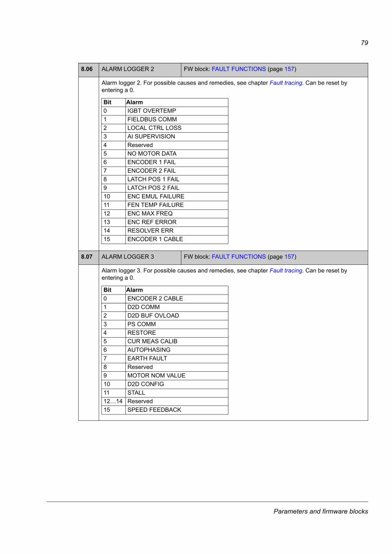
79
8.06 ALARM LOGGER 2 FW block: FAULT FUNCTIONS (page 157)
Alarm logger 2. For possible causes and remedies, see chapter Fault tracing. Can be reset by entering a 0.
8.07 ALARM LOGGER 3 FW block: FAULT FUNCTIONS (page 157)
Alarm logger 3. For possible causes and remedies, see chapter Fault tracing. Can be reset by entering a 0.
Bit Alarm0 IGBT OVERTEMP1 FIELDBUS COMM2 LOCAL CTRL LOSS3 AI SUPERVISION4 Reserved5 NO MOTOR DATA6 ENCODER 1 FAIL7 ENCODER 2 FAIL8 LATCH POS 1 FAIL9 LATCH POS 2 FAIL10 ENC EMUL FAILURE11 FEN TEMP FAILURE12 ENC MAX FREQ13 ENC REF ERROR14 RESOLVER ERR15 ENCODER 1 CABLE
Bit Alarm0 ENCODER 2 CABLE1 D2D COMM2 D2D BUF OVLOAD3 PS COMM4 RESTORE5 CUR MEAS CALIB6 AUTOPHASING7 EARTH FAULT8 Reserved9 MOTOR NOM VALUE10 D2D CONFIG11 STALL12…14 Reserved15 SPEED FEEDBACK
Parameters and firmware blocks

80
8.08 ALARM LOGGER 4 FW block: FAULT FUNCTIONS (page 157)
Alarm logger 4. For possible causes and remedies, see chapter Fault tracing. Can be reset by entering a 0.
8.09 ALARM LOGGER 5 FW block: FAULT FUNCTIONS (page 157)
Alarm logger 5. For possible causes and remedies, see chapter Fault tracing. Can be reset by entering a 0.
8.10 ALARM LOGGER 6 FW block: FAULT FUNCTIONS (page 157)
Alarm logger 6. For possible causes and remedies, see chapter Fault tracing. Can be reset by entering a 0.
Bit Alarm0 OPTION COMM LOSS1 SOLUTION ALARM2…5 Reserved6 PROT. SET PASS7…8 Reserved9 DC NOT CHARGED10 SPEED TUNE FAIL11…15 Reserved
Bit Alarm0…15 Reserved
Bit Alarm0…1 Reserved2 LOW VOLT MOD CON3…15 Reserved
Parameters and firmware blocks
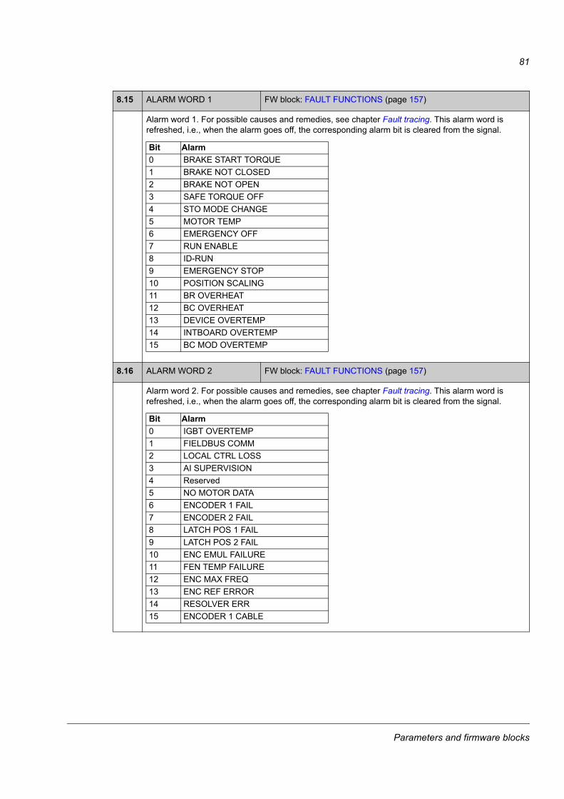
81
8.15 ALARM WORD 1 FW block: FAULT FUNCTIONS (page 157)
Alarm word 1. For possible causes and remedies, see chapter Fault tracing. This alarm word is refreshed, i.e., when the alarm goes off, the corresponding alarm bit is cleared from the signal.
8.16 ALARM WORD 2 FW block: FAULT FUNCTIONS (page 157)
Alarm word 2. For possible causes and remedies, see chapter Fault tracing. This alarm word is refreshed, i.e., when the alarm goes off, the corresponding alarm bit is cleared from the signal.
Bit Alarm0 BRAKE START TORQUE1 BRAKE NOT CLOSED2 BRAKE NOT OPEN3 SAFE TORQUE OFF4 STO MODE CHANGE5 MOTOR TEMP6 EMERGENCY OFF7 RUN ENABLE8 ID-RUN9 EMERGENCY STOP10 POSITION SCALING11 BR OVERHEAT12 BC OVERHEAT 13 DEVICE OVERTEMP 14 INTBOARD OVERTEMP15 BC MOD OVERTEMP
Bit Alarm0 IGBT OVERTEMP1 FIELDBUS COMM2 LOCAL CTRL LOSS3 AI SUPERVISION4 Reserved5 NO MOTOR DATA6 ENCODER 1 FAIL7 ENCODER 2 FAIL8 LATCH POS 1 FAIL9 LATCH POS 2 FAIL10 ENC EMUL FAILURE11 FEN TEMP FAILURE12 ENC MAX FREQ13 ENC REF ERROR14 RESOLVER ERR15 ENCODER 1 CABLE
Parameters and firmware blocks
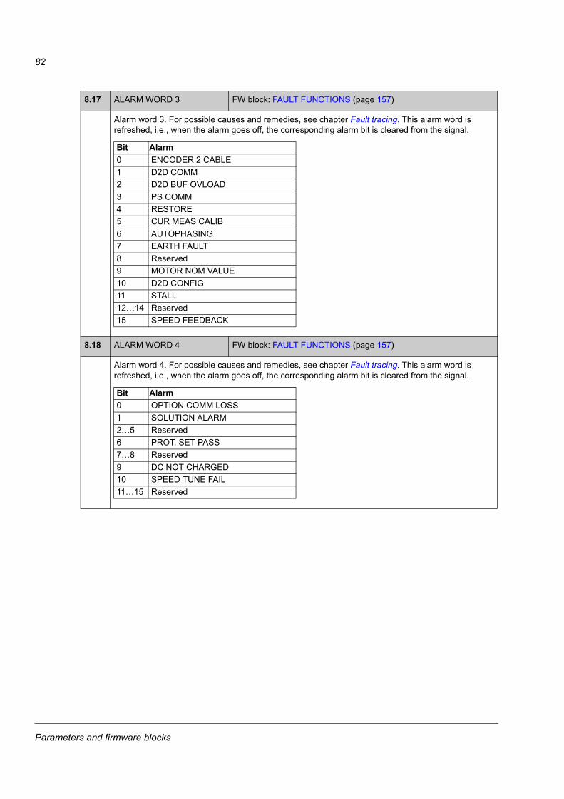
82
8.17 ALARM WORD 3 FW block: FAULT FUNCTIONS (page 157)
Alarm word 3. For possible causes and remedies, see chapter Fault tracing. This alarm word is refreshed, i.e., when the alarm goes off, the corresponding alarm bit is cleared from the signal.
8.18 ALARM WORD 4 FW block: FAULT FUNCTIONS (page 157)
Alarm word 4. For possible causes and remedies, see chapter Fault tracing. This alarm word is refreshed, i.e., when the alarm goes off, the corresponding alarm bit is cleared from the signal.
Bit Alarm0 ENCODER 2 CABLE1 D2D COMM2 D2D BUF OVLOAD3 PS COMM4 RESTORE5 CUR MEAS CALIB6 AUTOPHASING7 EARTH FAULT8 Reserved9 MOTOR NOM VALUE10 D2D CONFIG11 STALL12…14 Reserved15 SPEED FEEDBACK
Bit Alarm0 OPTION COMM LOSS1 SOLUTION ALARM2…5 Reserved6 PROT. SET PASS7…8 Reserved9 DC NOT CHARGED10 SPEED TUNE FAIL11…15 Reserved
Parameters and firmware blocks
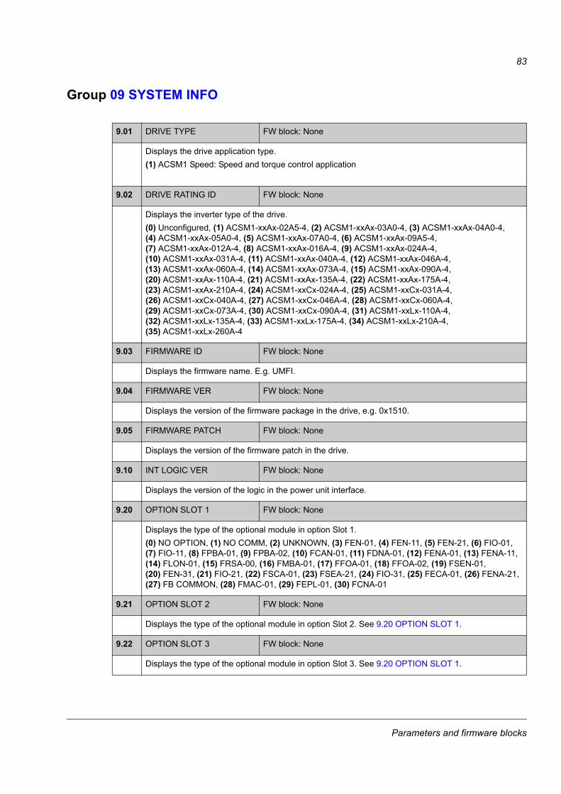
83
Group 09 SYSTEM INFO
099.01 DRIVE TYPE FW block: None
Displays the drive application type.(1) ACSM1 Speed: Speed and torque control application
9.02 DRIVE RATING ID FW block: None
Displays the inverter type of the drive.(0) Unconfigured, (1) ACSM1-xxAx-02A5-4, (2) ACSM1-xxAx-03A0-4, (3) ACSM1-xxAx-04A0-4, (4) ACSM1-xxAx-05A0-4, (5) ACSM1-xxAx-07A0-4, (6) ACSM1-xxAx-09A5-4, (7) ACSM1-xxAx-012A-4, (8) ACSM1-xxAx-016A-4, (9) ACSM1-xxAx-024A-4, (10) ACSM1-xxAx-031A-4, (11) ACSM1-xxAx-040A-4, (12) ACSM1-xxAx-046A-4, (13) ACSM1-xxAx-060A-4, (14) ACSM1-xxAx-073A-4, (15) ACSM1-xxAx-090A-4, (20) ACSM1-xxAx-110A-4, (21) ACSM1-xxAx-135A-4, (22) ACSM1-xxAx-175A-4, (23) ACSM1-xxAx-210A-4, (24) ACSM1-xxCx-024A-4, (25) ACSM1-xxCx-031A-4, (26) ACSM1-xxCx-040A-4, (27) ACSM1-xxCx-046A-4, (28) ACSM1-xxCx-060A-4, (29) ACSM1-xxCx-073A-4, (30) ACSM1-xxCx-090A-4, (31) ACSM1-xxLx-110A-4, (32) ACSM1-xxLx-135A-4, (33) ACSM1-xxLx-175A-4, (34) ACSM1-xxLx-210A-4, (35) ACSM1-xxLx-260A-4
9.03 FIRMWARE ID FW block: None
Displays the firmware name. E.g. UMFI.
9.04 FIRMWARE VER FW block: None
Displays the version of the firmware package in the drive, e.g. 0x1510.
9.05 FIRMWARE PATCH FW block: None
Displays the version of the firmware patch in the drive.
9.10 INT LOGIC VER FW block: None
Displays the version of the logic in the power unit interface.
9.20 OPTION SLOT 1 FW block: None
Displays the type of the optional module in option Slot 1.(0) NO OPTION, (1) NO COMM, (2) UNKNOWN, (3) FEN-01, (4) FEN-11, (5) FEN-21, (6) FIO-01, (7) FIO-11, (8) FPBA-01, (9) FPBA-02, (10) FCAN-01, (11) FDNA-01, (12) FENA-01, (13) FENA-11, (14) FLON-01, (15) FRSA-00, (16) FMBA-01, (17) FFOA-01, (18) FFOA-02, (19) FSEN-01, (20) FEN-31, (21) FIO-21, (22) FSCA-01, (23) FSEA-21, (24) FIO-31, (25) FECA-01, (26) FENA-21, (27) FB COMMON, (28) FMAC-01, (29) FEPL-01, (30) FCNA-01
9.21 OPTION SLOT 2 FW block: None
Displays the type of the optional module in option Slot 2. See 9.20 OPTION SLOT 1.
9.22 OPTION SLOT 3 FW block: None
Displays the type of the optional module in option Slot 3. See 9.20 OPTION SLOT 1.
Parameters and firmware blocks

84
Group 10 START/STOPSettings for
• selecting start/stop/direction signal sources for external control locations EXT1 and EXT2
• selecting sources for external fault reset, run enable and start enable signals
• selecting sources for emergency stop (OFF1 and OFF3)
• selecting source for jogging function activation signal
• enabling the start inhibit function.
See also section Jogging on page 47.
10Firmware block:DRIVE LOGIC(10)
This block• selects the sources for the start/
stop/direction signals for external control locations EXT1 and EXT2
• selects the sources for external fault reset, run enable and start enable signals
• selects the sources for emergency stop (OFF1 and OFF3)
• selects the source for jogging activation signal
• enables the start inhibit function.
DRIVE LOGIC21
TLF10 2 msec (3)
10.01 EXT1 START FUNC [ In1 ]
< 10.02 EXT1 START IN1 [ DI STATUS.0 ](2 / 2.01.DI1)
< 10.03 EXT1 START IN2 [ FALSE ]
10.04 EXT2 START FUNC [ In1 ]
< 10.05 EXT2 START IN1 [ DI STATUS.0 ](2 / 2.01.DI1)
< 10.06 EXT2 START IN2 [ FALSE ]
< 10.07 JOG1 START [ FALSE ]
< 10.08 FAULT RESET SEL [ DI STATUS.2 ](2 / 2.01.DI3)
< 10.09 RUN ENABLE [ TRUE ]
< 10.10 EM STOP OFF3 [ TRUE ]
< 10.11 EM STOP OFF1 [ TRUE ]
10.12 START INHIBIT [ Disabled ]
< 10.13 FB CW USED[ FBA MAIN CW ](4 / 2.12)
< 10.14 JOG2 START [ FALSE ]
< 10.15 JOG ENABLE [ FALSE ]
< 10.16 D2D CW USED[ D2D MAIN CW ](4 / 2.17)
< 10.17 START ENABLE [ TRUE ]
2.18 D2D FOLLOWER CW
6.01 STATUS WORD 1
6.02 STATUS WORD 2
6.03 SPEED CTRL STAT
6.05 LIMIT WORD 1
6.07 TORQ LIM STATUS
6.09 POS CTRL STATUS
6.10 POS CTRL STATUS2
6.11 POS CORR STATUS
Parameters and firmware blocks
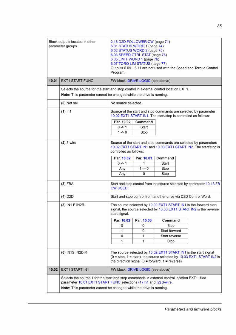
85
Block outputs located in other parameter groups
2.18 D2D FOLLOWER CW (page 71)6.01 STATUS WORD 1 (page 74)6.02 STATUS WORD 2 (page 75)6.03 SPEED CTRL STAT (page 76)6.05 LIMIT WORD 1 (page 76)6.07 TORQ LIM STATUS (page 77)Outputs 6.09…6.11 are not used with the Speed and Torque Control Program.
10.01 EXT1 START FUNC FW block: DRIVE LOGIC (see above)
Selects the source for the start and stop control in external control location EXT1. Note: This parameter cannot be changed while the drive is running.
(0) Not sel No source selected.
(1) In1 Source of the start and stop commands are selected by parameter 10.02 EXT1 START IN1. The start/stop is controlled as follows:
(2) 3-wire Source of the start and stop commands are selected by parameters 10.02 EXT1 START IN1 and 10.03 EXT1 START IN2. The start/stop is controlled as follows:
(3) FBA Start and stop control from the source selected by parameter 10.13 FB CW USED.
(4) D2D Start and stop control from another drive via D2D Control Word.
(5) IN1 F IN2R The source selected by 10.02 EXT1 START IN1 is the forward start signal, the source selected by 10.03 EXT1 START IN2 is the reverse start signal.
(6) IN1S IN2DIR The source selected by 10.02 EXT1 START IN1 is the start signal (0 = stop, 1 = start), the source selected by 10.03 EXT1 START IN2 is the direction signal (0 = forward, 1 = reverse).
10.02 EXT1 START IN1 FW block: DRIVE LOGIC (see above)
Selects the source 1 for the start and stop commands in external control location EXT1. See parameter 10.01 EXT1 START FUNC selections (1) In1 and (2) 3-wire.Note: This parameter cannot be changed while the drive is running.
Par. 10.02 Command0 -> 1 Start1 -> 0 Stop
Par. 10.02 Par. 10.03 Command0 -> 1 1 StartAny 1 -> 0 StopAny 0 Stop
Par. 10.02 Par. 10.03 Command0 0 Stop1 0 Start forward0 1 Start reverse1 1 Stop
Parameters and firmware blocks
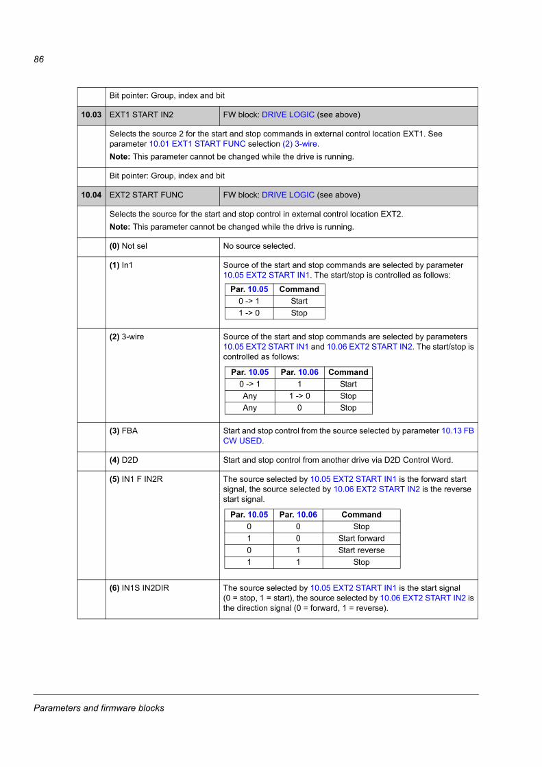
86
Bit pointer: Group, index and bit
10.03 EXT1 START IN2 FW block: DRIVE LOGIC (see above)
Selects the source 2 for the start and stop commands in external control location EXT1. See parameter 10.01 EXT1 START FUNC selection (2) 3-wire.Note: This parameter cannot be changed while the drive is running.
Bit pointer: Group, index and bit
10.04 EXT2 START FUNC FW block: DRIVE LOGIC (see above)
Selects the source for the start and stop control in external control location EXT2.Note: This parameter cannot be changed while the drive is running.
(0) Not sel No source selected.
(1) In1 Source of the start and stop commands are selected by parameter 10.05 EXT2 START IN1. The start/stop is controlled as follows:
(2) 3-wire Source of the start and stop commands are selected by parameters 10.05 EXT2 START IN1 and 10.06 EXT2 START IN2. The start/stop is controlled as follows:
(3) FBA Start and stop control from the source selected by parameter 10.13 FB CW USED.
(4) D2D Start and stop control from another drive via D2D Control Word.
(5) IN1 F IN2R The source selected by 10.05 EXT2 START IN1 is the forward start signal, the source selected by 10.06 EXT2 START IN2 is the reverse start signal.
(6) IN1S IN2DIR The source selected by 10.05 EXT2 START IN1 is the start signal (0 = stop, 1 = start), the source selected by 10.06 EXT2 START IN2 is the direction signal (0 = forward, 1 = reverse).
Par. 10.05 Command0 -> 1 Start1 -> 0 Stop
Par. 10.05 Par. 10.06 Command0 -> 1 1 StartAny 1 -> 0 StopAny 0 Stop
Par. 10.05 Par. 10.06 Command0 0 Stop1 0 Start forward0 1 Start reverse1 1 Stop
Parameters and firmware blocks
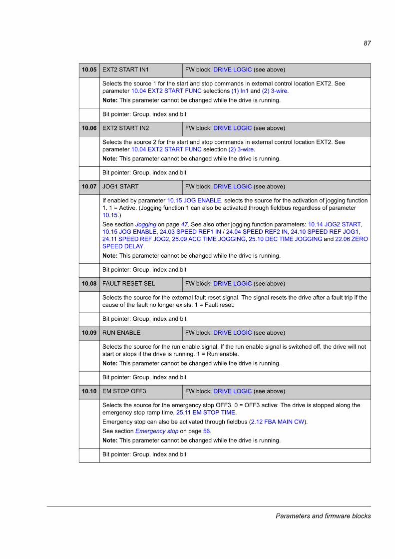
87
10.05 EXT2 START IN1 FW block: DRIVE LOGIC (see above)
Selects the source 1 for the start and stop commands in external control location EXT2. See parameter 10.04 EXT2 START FUNC selections (1) In1 and (2) 3-wire.Note: This parameter cannot be changed while the drive is running.
Bit pointer: Group, index and bit
10.06 EXT2 START IN2 FW block: DRIVE LOGIC (see above)
Selects the source 2 for the start and stop commands in external control location EXT2. See parameter 10.04 EXT2 START FUNC selection (2) 3-wire.Note: This parameter cannot be changed while the drive is running.
Bit pointer: Group, index and bit
10.07 JOG1 START FW block: DRIVE LOGIC (see above)
If enabled by parameter 10.15 JOG ENABLE, selects the source for the activation of jogging function 1. 1 = Active. (Jogging function 1 can also be activated through fieldbus regardless of parameter 10.15.)See section Jogging on page 47. See also other jogging function parameters: 10.14 JOG2 START, 10.15 JOG ENABLE, 24.03 SPEED REF1 IN / 24.04 SPEED REF2 IN, 24.10 SPEED REF JOG1, 24.11 SPEED REF JOG2, 25.09 ACC TIME JOGGING, 25.10 DEC TIME JOGGING and 22.06 ZERO SPEED DELAY.Note: This parameter cannot be changed while the drive is running.
Bit pointer: Group, index and bit
10.08 FAULT RESET SEL FW block: DRIVE LOGIC (see above)
Selects the source for the external fault reset signal. The signal resets the drive after a fault trip if the cause of the fault no longer exists. 1 = Fault reset.
Bit pointer: Group, index and bit
10.09 RUN ENABLE FW block: DRIVE LOGIC (see above)
Selects the source for the run enable signal. If the run enable signal is switched off, the drive will not start or stops if the drive is running. 1 = Run enable.Note: This parameter cannot be changed while the drive is running.
Bit pointer: Group, index and bit
10.10 EM STOP OFF3 FW block: DRIVE LOGIC (see above)
Selects the source for the emergency stop OFF3. 0 = OFF3 active: The drive is stopped along the emergency stop ramp time, 25.11 EM STOP TIME. Emergency stop can also be activated through fieldbus (2.12 FBA MAIN CW).See section Emergency stop on page 56.Note: This parameter cannot be changed while the drive is running.
Bit pointer: Group, index and bit
Parameters and firmware blocks
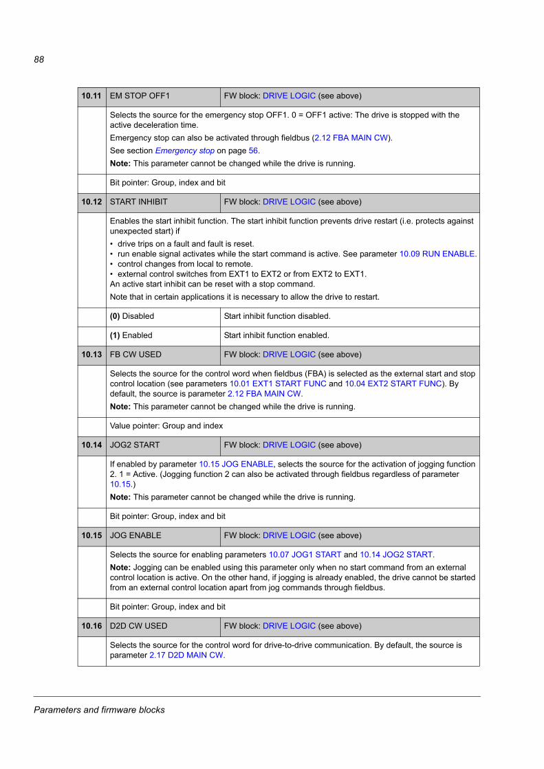
88
10.11 EM STOP OFF1 FW block: DRIVE LOGIC (see above)
Selects the source for the emergency stop OFF1. 0 = OFF1 active: The drive is stopped with the active deceleration time. Emergency stop can also be activated through fieldbus (2.12 FBA MAIN CW).See section Emergency stop on page 56.Note: This parameter cannot be changed while the drive is running.
Bit pointer: Group, index and bit
10.12 START INHIBIT FW block: DRIVE LOGIC (see above)
Enables the start inhibit function. The start inhibit function prevents drive restart (i.e. protects against unexpected start) if• drive trips on a fault and fault is reset.• run enable signal activates while the start command is active. See parameter 10.09 RUN ENABLE.• control changes from local to remote.• external control switches from EXT1 to EXT2 or from EXT2 to EXT1.An active start inhibit can be reset with a stop command.Note that in certain applications it is necessary to allow the drive to restart.
(0) Disabled Start inhibit function disabled.
(1) Enabled Start inhibit function enabled.
10.13 FB CW USED FW block: DRIVE LOGIC (see above)
Selects the source for the control word when fieldbus (FBA) is selected as the external start and stop control location (see parameters 10.01 EXT1 START FUNC and 10.04 EXT2 START FUNC). By default, the source is parameter 2.12 FBA MAIN CW.Note: This parameter cannot be changed while the drive is running.
Value pointer: Group and index
10.14 JOG2 START FW block: DRIVE LOGIC (see above)
If enabled by parameter 10.15 JOG ENABLE, selects the source for the activation of jogging function 2. 1 = Active. (Jogging function 2 can also be activated through fieldbus regardless of parameter 10.15.)Note: This parameter cannot be changed while the drive is running.
Bit pointer: Group, index and bit
10.15 JOG ENABLE FW block: DRIVE LOGIC (see above)
Selects the source for enabling parameters 10.07 JOG1 START and 10.14 JOG2 START.Note: Jogging can be enabled using this parameter only when no start command from an external control location is active. On the other hand, if jogging is already enabled, the drive cannot be started from an external control location apart from jog commands through fieldbus.
Bit pointer: Group, index and bit
10.16 D2D CW USED FW block: DRIVE LOGIC (see above)
Selects the source for the control word for drive-to-drive communication. By default, the source is parameter 2.17 D2D MAIN CW.
Parameters and firmware blocks

89
Value pointer: Group and index
10.17 START ENABLE FW block: DRIVE LOGIC (see above)
Selects the source for the start enable signal. If the start enable signal is switched off, the drive will not start or stops if the drive is running. 1 = Start enable.Note: This parameter cannot be changed while the drive is running.
Bit pointer: Group, index and bit
Parameters and firmware blocks
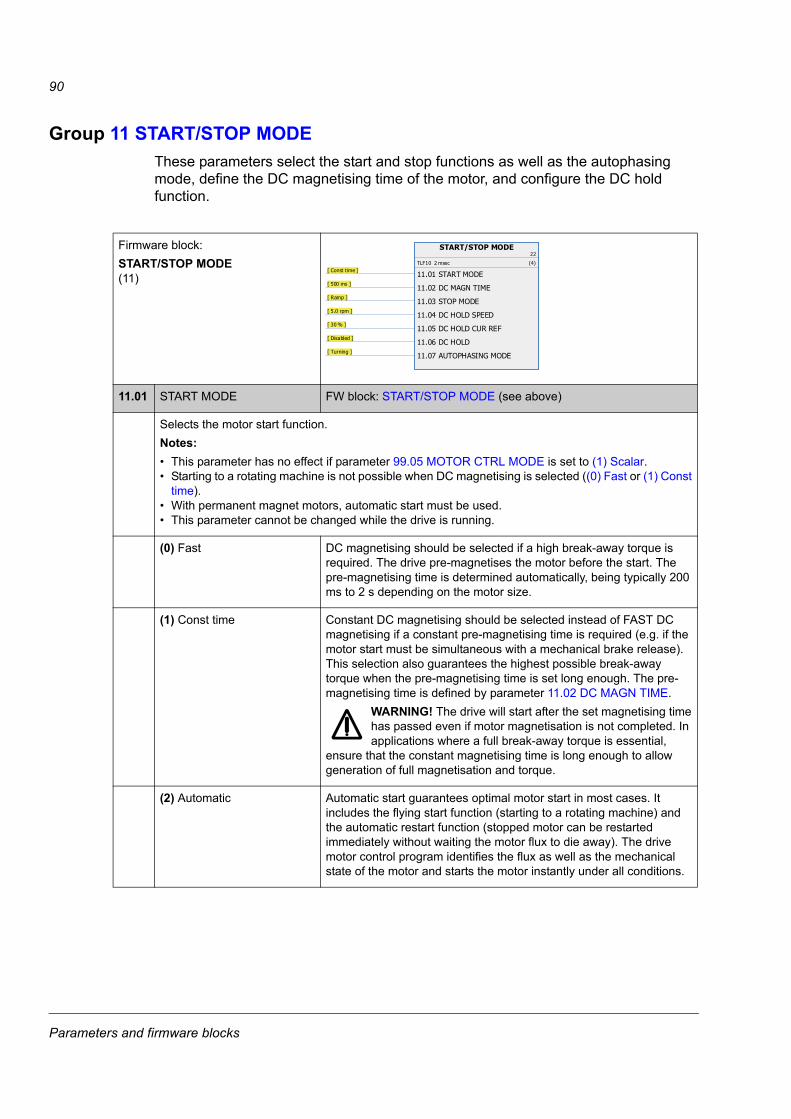
90
Group 11 START/STOP MODEThese parameters select the start and stop functions as well as the autophasing mode, define the DC magnetising time of the motor, and configure the DC hold function.
11Firmware block:START/STOP MODE(11)
11.01 START MODE FW block: START/STOP MODE (see above)
Selects the motor start function.Notes:• This parameter has no effect if parameter 99.05 MOTOR CTRL MODE is set to (1) Scalar.• Starting to a rotating machine is not possible when DC magnetising is selected ((0) Fast or (1) Const
time).• With permanent magnet motors, automatic start must be used.• This parameter cannot be changed while the drive is running.
(0) Fast DC magnetising should be selected if a high break-away torque is required. The drive pre-magnetises the motor before the start. The pre-magnetising time is determined automatically, being typically 200 ms to 2 s depending on the motor size.
(1) Const time Constant DC magnetising should be selected instead of FAST DC magnetising if a constant pre-magnetising time is required (e.g. if the motor start must be simultaneous with a mechanical brake release). This selection also guarantees the highest possible break-away torque when the pre-magnetising time is set long enough. The pre-magnetising time is defined by parameter 11.02 DC MAGN TIME.
WARNING! The drive will start after the set magnetising time has passed even if motor magnetisation is not completed. In applications where a full break-away torque is essential,
ensure that the constant magnetising time is long enough to allow generation of full magnetisation and torque.
(2) Automatic Automatic start guarantees optimal motor start in most cases. It includes the flying start function (starting to a rotating machine) and the automatic restart function (stopped motor can be restarted immediately without waiting the motor flux to die away). The drive motor control program identifies the flux as well as the mechanical state of the motor and starts the motor instantly under all conditions.
START/STOP MODE22
TLF10 2 msec (4)
11.01 START MODE [ Const time ]
11.02 DC MAGN TIME [ 500 ms ]
11.03 STOP MODE [ Ramp ]
11.04 DC HOLD SPEED [ 5.0 rpm ]
11.05 DC HOLD CUR REF [ 30 % ]
11.06 DC HOLD [ Disabled ]
11.07 AUTOPHASING MODE [ Turning ]
Parameters and firmware blocks
91
11.02 DC MAGN TIME FW block: START/STOP MODE (see above)
Defines the constant DC magnetising time. See parameter 11.01 START MODE. After the start command, the drive automatically premagnetises the motor the set time.To ensure full magnetising, set this value to the same value as or higher than the rotor time constant. If not known, use the rule-of-thumb value given in the table below:
Note: This parameter cannot be changed while the drive is running.
0…10000 ms DC magnetising time.
11.03 STOP MODE FW block: START/STOP MODE (see above)
Selects the motor stop function.
(1) Coast Stop by cutting of the motor power supply. The motor coasts to a stop.WARNING! If the mechanical brake is used, ensure it is safe to stop the drive by coasting. For more information on mechanical brake function, see parameter group 35.
(2) Ramp Stop along ramp. See parameter group 25.
11.04 DC HOLD SPEED FW block: START/STOP MODE (see above)
Defines the DC hold speed. See parameter 11.06 DC HOLD.
0…1000 rpm DC hold speed.
11.05 DC HOLD CUR REF FW block: START/STOP MODE (see above)
Defines the DC hold current in percent of the motor nominal current. See parameter 11.06 DC HOLD.
0…100% DC hold current.
Motor rated power Constant magnetising time< 1 kW > 50 to 100 ms
1 to 10 kW > 100 to 200 ms
10 to 200 kW > 200 to 1000 ms
200 to 1000 kW > 1000 to 2000 ms
Parameters and firmware blocks
92
11.06 DC HOLD FW block: START/STOP MODE (see above)
Enables the DC hold function. The function makes it possible to lock the rotor at zero speed.When both the reference and the speed drop below the value of parameter 11.04 DC HOLD SPEED, the drive will stop generating sinusoidal current and start to inject DC into the motor. The current is set by parameter 11.05 DC HOLD CUR REF. When the reference speed exceeds parameter 11.04 DC HOLD SPEED, normal drive operation continues.
Notes:• The DC hold function has no effect if the start signal is switched off.• The DC hold function can only be activated in speed control mode.• The DC hold function cannot be activated if par. 99.05 MOTOR CTRL MODE is set to (1) Scalar.• Injecting DC current into the motor causes the motor to heat up. In applications where long DC hold
times are required, externally ventilated motors should be used. If the DC hold period is long, the DC hold cannot prevent the motor shaft from rotating if a constant load is applied to the motor.
(0) Disabled DC hold function disabled.
(1) Enabled DC hold function enabled.
11.07 AUTOPHASING MODE FW block: START/STOP MODE (see above)
Selects the way the autophasing routine is performed. See also section Autophasing on page 38.
(0) Turning This mode gives the most accurate autophasing result. This mode can be used, and is recommended if it is allowed for the motor to rotate and the start-up is not time-critical. Note: This mode will cause the motor to rotate during the ID run.
(1) Standstill 1 Faster than the (0) Turning mode, but not as accurate. The motor will not rotate.
(2) Standstill 2 An alternative standstill autophasing mode that can be used if the TURNING mode cannot be used, and the (1) Standstill 1 mode gives erratic results. However, this mode is considerably slower than (1) Standstill 1.
t
t
DC HoldMotor speed
Reference
11.04 DC HOLD SPEED
Parameters and firmware blocks
93
Group 12 DIGITAL IOSettings for the digital inputs and outputs, and the relay output.
12Firmware block:DIO1(6)
Selects whether DIO1 is used as a digital input or as a digital output and connects an actual signal to the digital output. The block also shows the DIO status.
Block outputs located in other parameter groups
2.03 DIO STATUS (page 66)
Firmware block:DIO2(7)
Selects whether DIO2 is used as a digital or frequency input or as a digital output and connects an actual signal to the digital output. The block also shows the DIO status.Frequency input can be scaled with standard function blocks. See chapter Standard function blocks.
Block outputs located in other parameter groups
2.03 DIO STATUS (page 66)2.10 DIO2 FREQ IN (page 66)
Firmware block:DIO3(8)
Selects whether DIO3 is used as a digital input or as a digital/frequency output, connects an actual signal to the digital/frequency output and scales the frequency output. The block also shows the DIO status.
Block outputs located in other parameter groups
2.03 DIO STATUS (page 66)2.11 DIO3 FREQ OUT (page 66)
12.01 DIO1 CONF FW block: DIO1 (see above)
Selects whether DIO1 is used as a digital input or as a digital output.
(0) Output DIO1 is used as a digital output.
(1) Input DIO1 is used as a digital input.
DIO118
TLF7 2 msec (3)
12.01 DIO1 CONF [ Output ]
< 12.04 DIO1 OUT PTR [ STATUS WORD 2.2 ](4 / 6.02.READY RELAY)
2.03 DIO STATUS 2.03Bit 0
DIO219
TLF7 2 msec (4)
12.02 DIO2 CONF [ Output ]
< 12.05 DIO2 OUT PTR [ STATUS WORD 2.3 ](4 / 6.02.MODULATING)
12.14 DIO2 F MAX [ 1000 Hz ]
12.15 DIO2 F MIN [ 3 Hz ]
12.16 DIO2 F MAX SCALE [ 1500 ]
12.17 DIO2 F MIN SCALE [ 0 ]
2.03 DIO STATUS 2.03Bit 1
2.10 DIO2 FREQ IN
DIO320
TLF7 2 msec (5)
12.03 DIO3 CONF [ Output ]
< 12.06 DIO3 OUT PTR [ STATUS WORD 1.10 ](4 / 6.01.FAULT)
< 12.07 DIO3 F OUT PTR[ SPEED ACT ](7 / 1.01)
12.08 DIO3 F MAX [ 1000 Hz ]
12.09 DIO3 F MIN [ 3 Hz ]
12.10 DIO3 F MAX SCALE [ 1500 ]
12.11 DIO3 F MIN SCALE [ 0 ]
2.03 DIO STATUS 2.03Bit 2
2.11 DIO3 FREQ OUT
Parameters and firmware blocks
94
12.02 DIO2 CONF FW block: DIO2 (see above)
Selects whether DIO2 is used as a digital input, as a digital output or as a frequency input.
(0) Output DIO2 is used as a digital output.
(1) Input DIO2 is used as a digital input.
(2) Freq input DIO2 is used as a frequency input.
12.03 DIO3 CONF FW block: DIO3 (see above)
Selects whether DIO3 is used as a digital input, as a digital output or as a frequency output.
(0) Output DIO2 is used as a digital output.
(1) Input DIO2 is used as a digital input.
(2) Freq output DIO2 is used as a frequency output.
12.04 DIO1 OUT PTR FW block: DIO1 (see above)
Selects a drive signal to be connected to digital output DIO1 (when 12.01 DIO1 CONF is set to (0) Output).
Bit pointer: Group, index and bit
12.05 DIO2 OUT PTR FW block: DIO2 (see above)
Selects a drive signal to be connected to digital output DIO2 (when 12.02 DIO2 CONF is set to (0) Output).
Bit pointer: Group, index and bit
12.06 DIO3 OUT PTR FW block: DIO3 (see above)
Selects a drive signal to be connected to digital output DIO3 (when 12.03 DIO3 CONF is set to (0) Output).
Bit pointer: Group, index and bit
12.07 DIO3 F OUT PTR FW block: DIO3 (see above)
Selects a drive signal to be connected to frequency output (when 12.03 DIO3 CONF is set to (2) Freq output).
Value pointer: Group and index
12.08 DIO3 F MAX FW block: DIO3 (see above)
When 12.03 DIO3 CONF is set to (2) Freq output, defines the maximum DIO3 output frequency.
3…32768 Hz Maximum DIO3 output frequency.
12.09 DIO3 F MIN FW block: DIO3 (see above)
When 12.03 DIO3 CONF is set to (2) Freq output, defines the minimum DIO3 output frequency.
3…32768 Hz Minimum DIO3 output frequency.
Parameters and firmware blocks
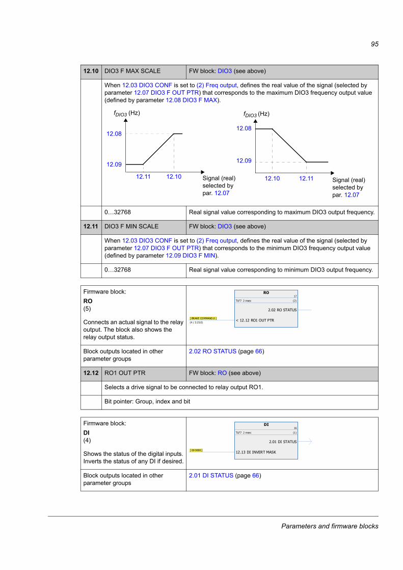
95
12.10 DIO3 F MAX SCALE FW block: DIO3 (see above)
When 12.03 DIO3 CONF is set to (2) Freq output, defines the real value of the signal (selected by parameter 12.07 DIO3 F OUT PTR) that corresponds to the maximum DIO3 frequency output value (defined by parameter 12.08 DIO3 F MAX).
0…32768 Real signal value corresponding to maximum DIO3 output frequency.
12.11 DIO3 F MIN SCALE FW block: DIO3 (see above)
When 12.03 DIO3 CONF is set to (2) Freq output, defines the real value of the signal (selected by parameter 12.07 DIO3 F OUT PTR) that corresponds to the minimum DIO3 frequency output value (defined by parameter 12.09 DIO3 F MIN).
0…32768 Real signal value corresponding to minimum DIO3 output frequency.
Firmware block:RO(5)
Connects an actual signal to the relay output. The block also shows the relay output status.
Block outputs located in other parameter groups
2.02 RO STATUS (page 66)
12.12 RO1 OUT PTR FW block: RO (see above)
Selects a drive signal to be connected to relay output RO1.
Bit pointer: Group, index and bit
Firmware block:DI(4)
Shows the status of the digital inputs. Inverts the status of any DI if desired.
Block outputs located in other parameter groups
2.01 DI STATUS (page 66)
fDIO3 (Hz)
12.08
12.09
12.10 12.1112.1012.11
12.08
12.09
Signal (real) selected by par. 12.07
fDIO3 (Hz)
Signal (real) selected by par. 12.07
RO17
TLF7 2 msec (2)
< 12.12 RO1 OUT PTR [ BRAKE COMMAND.0 ](4 / 3.15.0)
2.02 RO STATUS
DI16
TLF7 2 msec (1)
12.13 DI INVERT MASK [ 00 0000 ]
2.01 DI STATUS
Parameters and firmware blocks
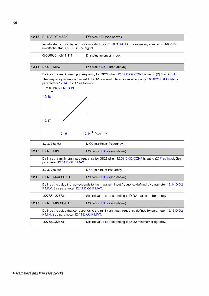
96
12.13 DI INVERT MASK FW block: DI (see above)
Inverts status of digital inputs as reported by 2.01 DI STATUS. For example, a value of 0b000100 inverts the status of DI3 in the signal.
0b000000…0b111111 DI status inversion mask.
12.14 DIO2 F MAX FW block: DIO2 (see above)
Defines the maximum input frequency for DIO2 when 12.02 DIO2 CONF is set to (2) Freq input. The frequency signal connected to DIO2 is scaled into an internal signal (2.10 DIO2 FREQ IN) by parameters 12.14…12.17 as follows:
3…32768 Hz DIO2 maximum frequency.
12.15 DIO2 F MIN FW block: DIO2 (see above)
Defines the minimum input frequency for DIO2 when 12.02 DIO2 CONF is set to (2) Freq input. See parameter 12.14 DIO2 F MAX
3…32768 Hz DIO2 minimum frequency.
12.16 DIO2 F MAX SCALE FW block: DIO2 (see above)
Defines the value that corresponds to the maximum input frequency defined by parameter 12.14 DIO2 F MAX. See parameter 12.14 DIO2 F MAX.
-32768…32768 Scaled value corresponding to DIO2 maximum frequency.
12.17 DIO2 F MIN SCALE FW block: DIO2 (see above)
Defines the value that corresponds to the minimum input frequency defined by parameter 12.15 DIO2 F MIN. See parameter 12.14 DIO2 F MAX.
-32768…32768 Scaled value corresponding to DIO2 minimum frequency.
fDIO2 (Hz)12.14
12.16
12.17
12.15
2.10 DIO2 FREQ IN
Parameters and firmware blocks
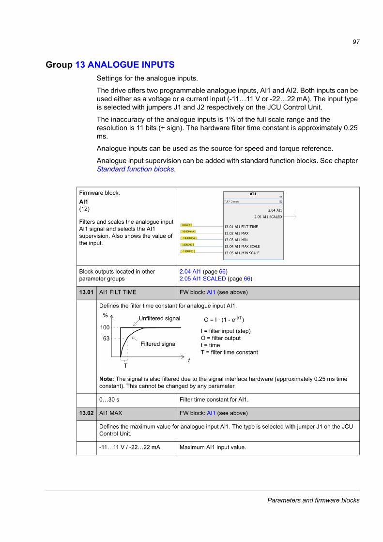
97
Group 13 ANALOGUE INPUTSSettings for the analogue inputs.
The drive offers two programmable analogue inputs, AI1 and AI2. Both inputs can be used either as a voltage or a current input (-11…11 V or -22…22 mA). The input type is selected with jumpers J1 and J2 respectively on the JCU Control Unit.
The inaccuracy of the analogue inputs is 1% of the full scale range and the resolution is 11 bits (+ sign). The hardware filter time constant is approximately 0.25 ms.
Analogue inputs can be used as the source for speed and torque reference.
Analogue input supervision can be added with standard function blocks. See chapter Standard function blocks.
13Firmware block:AI1(12)
Filters and scales the analogue input AI1 signal and selects the AI1 supervision. Also shows the value of the input.
Block outputs located in other parameter groups
2.04 AI1 (page 66)2.05 AI1 SCALED (page 66)
13.01 AI1 FILT TIME FW block: AI1 (see above)
Defines the filter time constant for analogue input AI1.
Note: The signal is also filtered due to the signal interface hardware (approximately 0.25 ms time constant). This cannot be changed by any parameter.
0…30 s Filter time constant for AI1.
13.02 AI1 MAX FW block: AI1 (see above)
Defines the maximum value for analogue input AI1. The type is selected with jumper J1 on the JCU Control Unit.
-11…11 V / -22…22 mA Maximum AI1 input value.
AI123
TLF7 2 msec (6)
13.01 AI1 FILT TIME [ 0.000 s ]
13.02 AI1 MAX [ 10.000 mA ]
13.03 AI1 MIN [ -10.000 mA ]
13.04 AI1 MAX SCALE [ 1500.000 ]
13.05 AI1 MIN SCALE [ -1500.000 ]
2.04 AI1
2.05 AI1 SCALED
63
%
100
Tt
Filtered signal
Unfiltered signal O = I · (1 - e-t/T)
I = filter input (step)O = filter outputt = timeT = filter time constant
Parameters and firmware blocks

98
13.03 AI1 MIN FW block: AI1 (see above)
Defines the minimum value for analogue input AI1. The type is selected with jumper J1 on the JCU Control Unit.
-11…11 V / -22…22 mA Minimum AI1 input value.
13.04 AI1 MAX SCALE FW block: AI1 (see above)
Defines the real value that corresponds to the maximum analogue input value defined by parameter 13.02 AI1 MAX.
-32768…32768 Real value corresponding to value of parameter 13.02.
13.05 AI1 MIN SCALE FW block: AI1 (see above)
Defines the real value that corresponds to the minimum analogue input value defined by parameter 13.03 AI1 MIN. See parameter 13.04 AI1 MAX SCALE.
-32768…32768 Real value corresponding to value of parameter 13.03.
Firmware block:AI2(13)
Filters and scales the analogue input AI2 signal and selects the AI2 supervision. Also shows the value of the input.
Block outputs located in other parameter groups
2.06 AI2 (page 66)2.07 AI2 SCALED (page 66)
13.06 AI2 FILT TIME FW block: AI2 (see above)
Defines the filter time constant for analogue input AI2. See parameter 13.01 AI1 FILT TIME.
0…30 s Filter time constant for AI2.
AI (scaled)
AI (mA / V)13.0213.03
13.05
13.04
AI224
TLF7 2 msec (7)
13.06 AI2 FILT TIME [ 0.000 s ]
13.07 AI2 MAX [ 10.000 mA ]
13.08 AI2 MIN [ -10.000 mA ]
13.09 AI2 MAX SCALE [ 100.000 ]
13.10 AI2 MIN SCALE [ -100.000 ]
2.06 AI2
2.07 AI2 SCALED
Parameters and firmware blocks
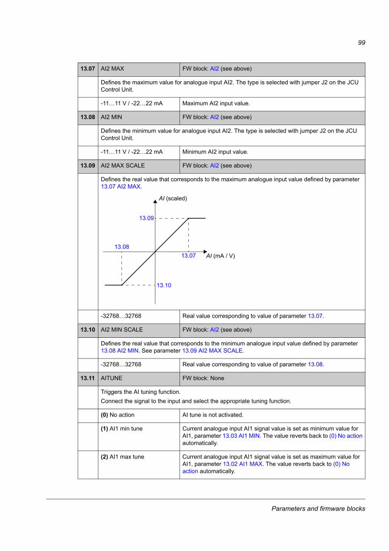
99
13.07 AI2 MAX FW block: AI2 (see above)
Defines the maximum value for analogue input AI2. The type is selected with jumper J2 on the JCU Control Unit.
-11…11 V / -22…22 mA Maximum AI2 input value.
13.08 AI2 MIN FW block: AI2 (see above)
Defines the minimum value for analogue input AI2. The type is selected with jumper J2 on the JCU Control Unit.
-11…11 V / -22…22 mA Minimum AI2 input value.
13.09 AI2 MAX SCALE FW block: AI2 (see above)
Defines the real value that corresponds to the maximum analogue input value defined by parameter 13.07 AI2 MAX.
-32768…32768 Real value corresponding to value of parameter 13.07.
13.10 AI2 MIN SCALE FW block: AI2 (see above)
Defines the real value that corresponds to the minimum analogue input value defined by parameter 13.08 AI2 MIN. See parameter 13.09 AI2 MAX SCALE.
-32768…32768 Real value corresponding to value of parameter 13.08.
13.11 AITUNE FW block: None
Triggers the AI tuning function.Connect the signal to the input and select the appropriate tuning function.
(0) No action AI tune is not activated.
(1) AI1 min tune Current analogue input AI1 signal value is set as minimum value for AI1, parameter 13.03 AI1 MIN. The value reverts back to (0) No action automatically.
(2) AI1 max tune Current analogue input AI1 signal value is set as maximum value for AI1, parameter 13.02 AI1 MAX. The value reverts back to (0) No action automatically.
AI (scaled)
AI (mA / V)13.0713.08
13.10
13.09
Parameters and firmware blocks
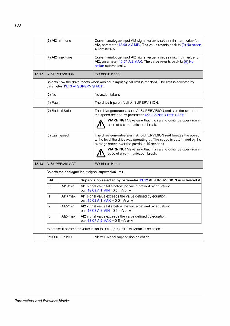
100
(3) AI2 min tune Current analogue input AI2 signal value is set as minimum value for AI2, parameter 13.08 AI2 MIN. The value reverts back to (0) No action automatically.
(4) AI2 max tune Current analogue input AI2 signal value is set as maximum value for AI2, parameter 13.07 AI2 MAX. The value reverts back to (0) No action automatically.
13.12 AI SUPERVISION FW block: None
Selects how the drive reacts when analogue input signal limit is reached. The limit is selected by parameter 13.13 AI SUPERVIS ACT.
(0) No No action taken.
(1) Fault The drive trips on fault AI SUPERVISION.
(2) Spd ref Safe The drive generates alarm AI SUPERVISION and sets the speed to the speed defined by parameter 46.02 SPEED REF SAFE.
WARNING! Make sure that it is safe to continue operation in case of a communication break.
(3) Last speed The drive generates alarm AI SUPERVISION and freezes the speed to the level the drive was operating at. The speed is determined by the average speed over the previous 10 seconds.
WARNING! Make sure that it is safe to continue operation in case of a communication break.
13.13 AI SUPERVIS ACT FW block: None
Selects the analogue input signal supervision limit.
Example: If parameter value is set to 0010 (bin), bit 1 AI1>max is selected.
0b0000…0b1111 AI1/AI2 signal supervision selection.
Bit Supervision selected by parameter 13.12 AI SUPERVISION is activated if0 AI1<min AI1 signal value falls below the value defined by equation:
par. 13.03 AI1 MIN - 0.5 mA or V
1 AI1>max AI1 signal value exceeds the value defined by equation:par. 13.02 AI1 MAX + 0.5 mA or V
2 AI2<min AI2 signal value falls below the value defined by equation:par. 13.08 AI2 MIN - 0.5 mA or V
3 AI2>max AI2 signal value exceeds the value defined by equation:par. 13.07 AI2 MAX + 0.5 mA or V
Parameters and firmware blocks

101
Group 15 ANALOGUE OUTPUTSSettings for the analogue outputs.The drive offers two programmable analogue outputs: one current output AO1 (0…20 mA) and one voltage output AO2 (-10…10 V).
The resolution of the analogue outputs is 11 bits (+ sign) and the inaccuracy is 2% of the full scale range.
The analogue output signals can be proportional to motor speed, process speed (scaled motor speed), output frequency, output current, motor torque, motor power, etc. It is possible to write a value to an analogue output through a serial communication link (e.g. fieldbus link).
15Firmware block:AO1(14)
Connects an actual signal to analogue output AO1, and filters and scales the output signal. Also shows the value of the output.
Block outputs located in other parameter groups
2.08 AO1 (page 66)
15.01 AO1 PTR FW block: AO1 (see above)
Selects a drive signal to be connected to analogue output AO1.
Value pointer: Group and index
15.02 AO1 FILT TIME FW block: AO1 (see above)
Defines the filtering time constant for analogue output AO1.
Note: The signal is also filtered due to the signal interface hardware (approximately 0.5 ms time constant). This cannot be changed by any parameter.
0…30 s Filter time constant for AO1.
15.03 AO1 MAX FW block: AO1 (see above)
Defines the maximum value for analogue output AO1.
0…22.7 mA Maximum AO1 output value.
AO125
TLF7 2 msec (8)
< 15.01 AO1 PTR[ CURRENT PERC ](1 / 1.05)
15.02 AO1 FILT TIME [ 0.100 s ]
15.03 AO1 MAX [ 20.000 mA ]
15.04 AO1 MIN [ 4.000 mA ]
15.05 AO1 MAX SCALE [ 100.000 ]
15.06 AO1 MIN SCALE [ 0.000 ]
2.08 AO1
63
%
100
Tt
Filtered signal
Unfiltered signal O = I · (1 - e-t/T)
I = filter input (step)O = filter outputt = timeT = filter time constant
Parameters and firmware blocks
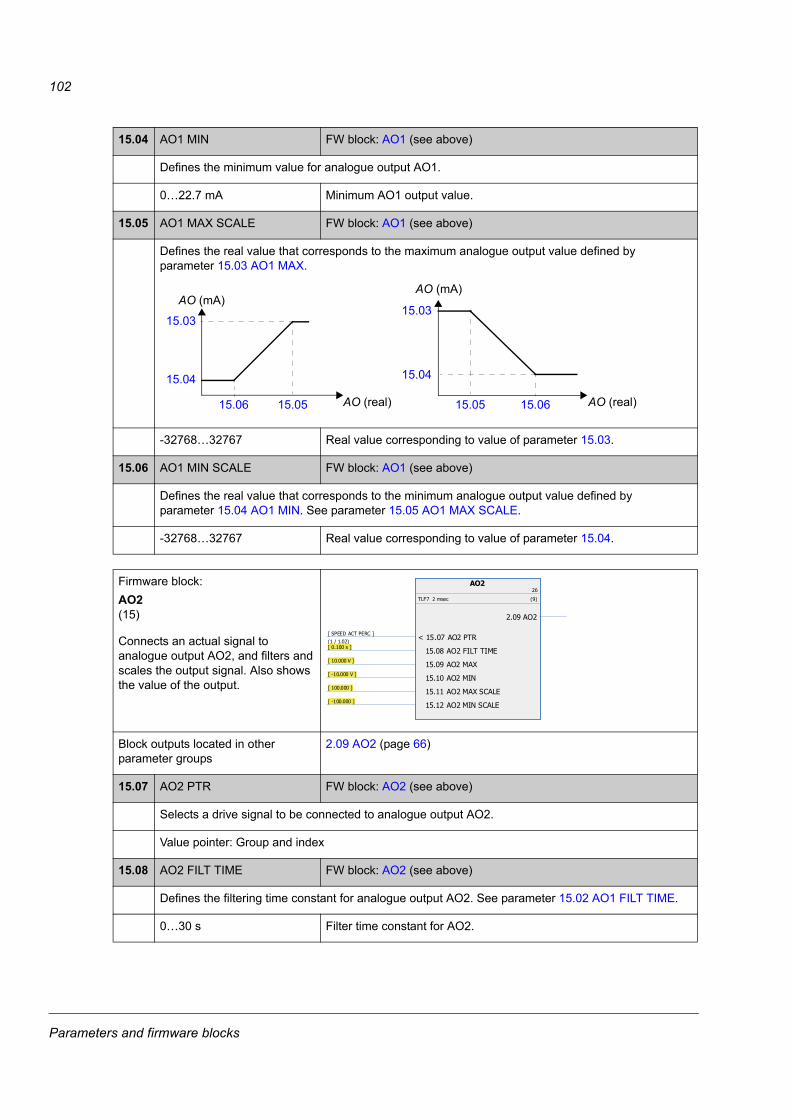
102
15.04 AO1 MIN FW block: AO1 (see above)
Defines the minimum value for analogue output AO1.
0…22.7 mA Minimum AO1 output value.
15.05 AO1 MAX SCALE FW block: AO1 (see above)
Defines the real value that corresponds to the maximum analogue output value defined by parameter 15.03 AO1 MAX.
-32768…32767 Real value corresponding to value of parameter 15.03.
15.06 AO1 MIN SCALE FW block: AO1 (see above)
Defines the real value that corresponds to the minimum analogue output value defined by parameter 15.04 AO1 MIN. See parameter 15.05 AO1 MAX SCALE.
-32768…32767 Real value corresponding to value of parameter 15.04.
Firmware block:AO2(15)
Connects an actual signal to analogue output AO2, and filters and scales the output signal. Also shows the value of the output.
Block outputs located in other parameter groups
2.09 AO2 (page 66)
15.07 AO2 PTR FW block: AO2 (see above)
Selects a drive signal to be connected to analogue output AO2.
Value pointer: Group and index
15.08 AO2 FILT TIME FW block: AO2 (see above)
Defines the filtering time constant for analogue output AO2. See parameter 15.02 AO1 FILT TIME.
0…30 s Filter time constant for AO2.
15.03
15.04
15.03
15.04
15.06 15.05 15.05 15.06 AO (real)AO (real)
AO (mA)AO (mA)
AO226
TLF7 2 msec (9)
< 15.07 AO2 PTR[ SPEED ACT PERC ](1 / 1.02)
15.08 AO2 FILT TIME [ 0.100 s ]
15.09 AO2 MAX [ 10.000 V ]
15.10 AO2 MIN [ -10.000 V ]
15.11 AO2 MAX SCALE [ 100.000 ]
15.12 AO2 MIN SCALE [ -100.000 ]
2.09 AO2
Parameters and firmware blocks

103
15.09 AO2 MAX FW block: AO2 (see above)
Defines the maximum value for analogue output AO2.
-10…10 V Maximum AO2 output value.
15.10 AO2 MIN FW block: AO2 (see above)
Defines the minimum value for analogue output AO2.
-10…10 V Minimum AO2 output value.
15.11 AO2 MAX SCALE FW block: AO2 (see above)
Defines the real value that corresponds to the maximum analogue output value defined by parameter 15.09 AO2 MAX.
-32768…32767 Real value corresponding to value of parameter 15.09.
15.12 AO2 MIN SCALE FW block: AO2 (see above)
Defines the real value that corresponds to the minimum analogue output value defined by parameter 15.10 AO2 MIN. See parameter 15.11 AO2 MAX SCALE.
-32768…32767 Real value corresponding to value of parameter 15.10.
15.09
15.10
15.09
15.10
15.12 15.11 15.11 15.12 AO (real)AO (real)
AO (V)AO (V)
Parameters and firmware blocks
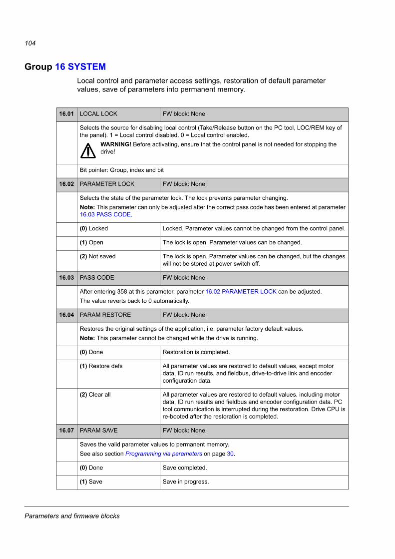
104
Group 16 SYSTEMLocal control and parameter access settings, restoration of default parameter values, save of parameters into permanent memory.
1616.01 LOCAL LOCK FW block: None
Selects the source for disabling local control (Take/Release button on the PC tool, LOC/REM key of the panel). 1 = Local control disabled. 0 = Local control enabled.
WARNING! Before activating, ensure that the control panel is not needed for stopping the drive!
Bit pointer: Group, index and bit
16.02 PARAMETER LOCK FW block: None
Selects the state of the parameter lock. The lock prevents parameter changing.Note: This parameter can only be adjusted after the correct pass code has been entered at parameter 16.03 PASS CODE.
(0) Locked Locked. Parameter values cannot be changed from the control panel.
(1) Open The lock is open. Parameter values can be changed.
(2) Not saved The lock is open. Parameter values can be changed, but the changes will not be stored at power switch off.
16.03 PASS CODE FW block: None
After entering 358 at this parameter, parameter 16.02 PARAMETER LOCK can be adjusted.The value reverts back to 0 automatically.
16.04 PARAM RESTORE FW block: None
Restores the original settings of the application, i.e. parameter factory default values.Note: This parameter cannot be changed while the drive is running.
(0) Done Restoration is completed.
(1) Restore defs All parameter values are restored to default values, except motor data, ID run results, and fieldbus, drive-to-drive link and encoder configuration data.
(2) Clear all All parameter values are restored to default values, including motor data, ID run results and fieldbus and encoder configuration data. PC tool communication is interrupted during the restoration. Drive CPU is re-booted after the restoration is completed.
16.07 PARAM SAVE FW block: None
Saves the valid parameter values to permanent memory.See also section Programming via parameters on page 30.
(0) Done Save completed.
(1) Save Save in progress.
Parameters and firmware blocks

105
16.09 USER SET SEL FW block: None
Enables the save and restoration of up to four custom sets of parameter settings.The set that was in use before powering down the drive is in use after the next power-up.Note: Any parameter changes made after loading a user set are not automatically stored into the loaded set – they must be saved using this parameter.
(1) No request Load or save operation complete; normal operation.
(2) Load set 1 Load user parameter set 1.
(3) Load set 2 Load user parameter set 2.
(4) Load set 3 Load user parameter set 3.
(5) Load set 4 Load user parameter set 4.
(6) Save set 1 Save user parameter set 1.
(7) Save set 2 Save user parameter set 2.
(8) Save set 3 Save user parameter set 3.
(9) Save set 4 Save user parameter set 4.
(10) IO mode Load user parameter set using parameters 16.11 and 16.12.
16.10 USER SET LOG FW block: None
Shows the status of the user parameter sets (see parameter 16.09 USER SET SEL). Read-only.
N/A No user sets have been saved.
(1) Loading A user set is being loaded.
(2) Saving A user set is being saved.
(4) Faulted Invalid or empty parameter set.
(8) Set1 IO act User parameter set 1 has been selected by parameters 16.11 and 16.12.
(16) Set2 IO act User parameter set 2 has been selected by parameters 16.11 and 16.12.
(32) Set3 IO act User parameter set 3 has been selected by parameters 16.11 and 16.12.
(64) Set4 IO act User parameter set 4 has been selected by parameters 16.11 and 16.12.
(128) Set1 par act User parameter set 1 has been loaded using parameter 16.09.
(256) Set2 par act User parameter set 2 has been loaded using parameter 16.09.
(512) Set3 par act User parameter set 3 has been loaded using parameter 16.09.
(1024) Set4 par act User parameter set 4 has been loaded using parameter 16.09.
Parameters and firmware blocks
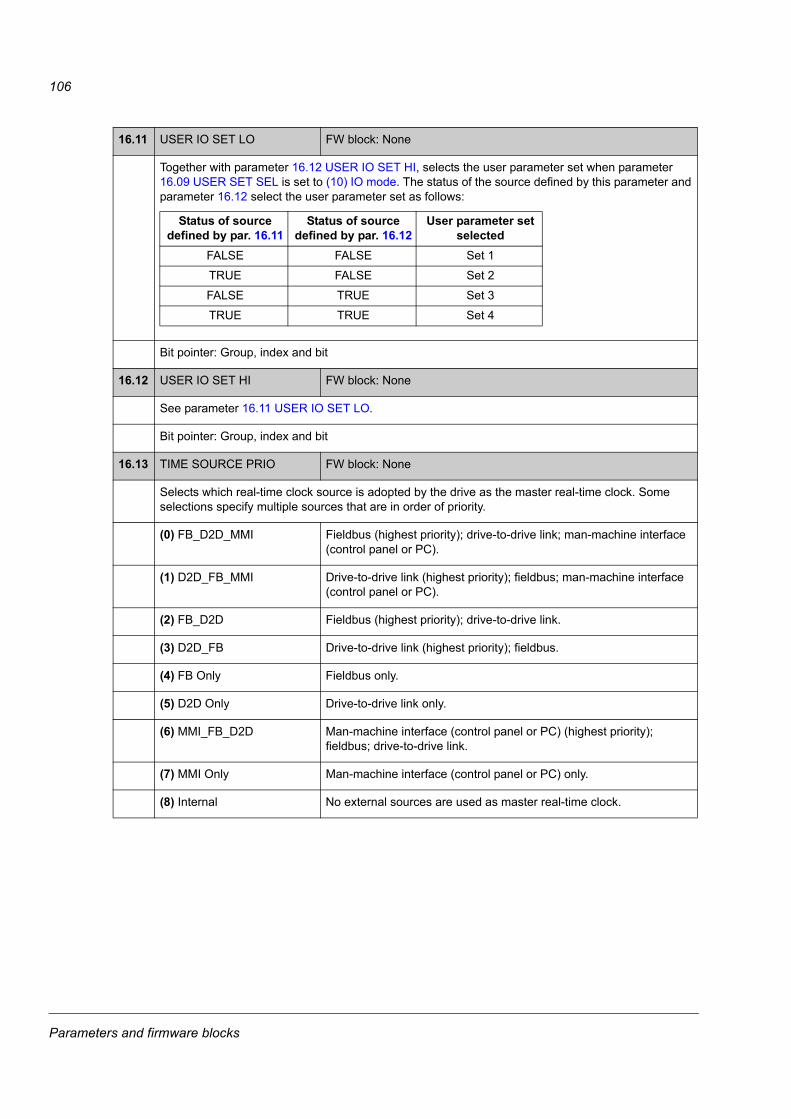
106
16.11 USER IO SET LO FW block: None
Together with parameter 16.12 USER IO SET HI, selects the user parameter set when parameter 16.09 USER SET SEL is set to (10) IO mode. The status of the source defined by this parameter and parameter 16.12 select the user parameter set as follows:
Bit pointer: Group, index and bit
16.12 USER IO SET HI FW block: None
See parameter 16.11 USER IO SET LO.
Bit pointer: Group, index and bit
16.13 TIME SOURCE PRIO FW block: None
Selects which real-time clock source is adopted by the drive as the master real-time clock. Some selections specify multiple sources that are in order of priority.
(0) FB_D2D_MMI Fieldbus (highest priority); drive-to-drive link; man-machine interface (control panel or PC).
(1) D2D_FB_MMI Drive-to-drive link (highest priority); fieldbus; man-machine interface (control panel or PC).
(2) FB_D2D Fieldbus (highest priority); drive-to-drive link.
(3) D2D_FB Drive-to-drive link (highest priority); fieldbus.
(4) FB Only Fieldbus only.
(5) D2D Only Drive-to-drive link only.
(6) MMI_FB_D2D Man-machine interface (control panel or PC) (highest priority); fieldbus; drive-to-drive link.
(7) MMI Only Man-machine interface (control panel or PC) only.
(8) Internal No external sources are used as master real-time clock.
Status of source defined by par. 16.11
Status of source defined by par. 16.12
User parameter set selected
FALSE FALSE Set 1
TRUE FALSE Set 2
FALSE TRUE Set 3
TRUE TRUE Set 4
Parameters and firmware blocks
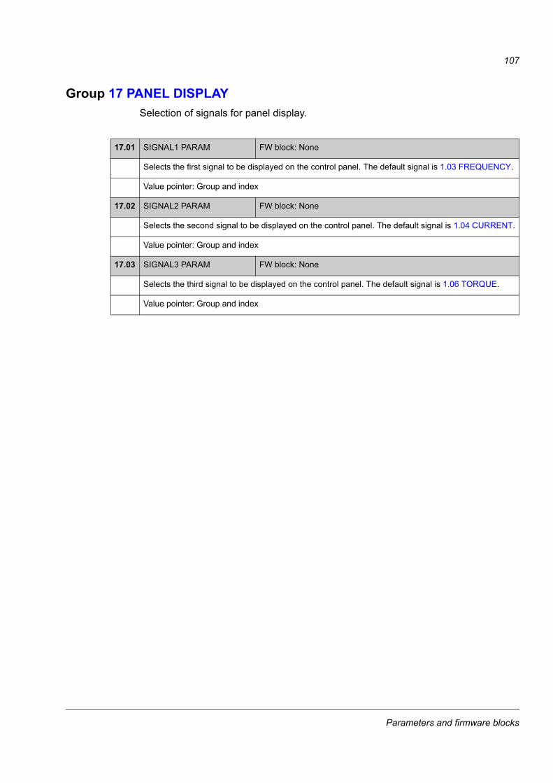
107
Group 17 PANEL DISPLAYSelection of signals for panel display.
1717.01 SIGNAL1 PARAM FW block: None
Selects the first signal to be displayed on the control panel. The default signal is 1.03 FREQUENCY.
Value pointer: Group and index
17.02 SIGNAL2 PARAM FW block: None
Selects the second signal to be displayed on the control panel. The default signal is 1.04 CURRENT.
Value pointer: Group and index
17.03 SIGNAL3 PARAM FW block: None
Selects the third signal to be displayed on the control panel. The default signal is 1.06 TORQUE.
Value pointer: Group and index
Parameters and firmware blocks
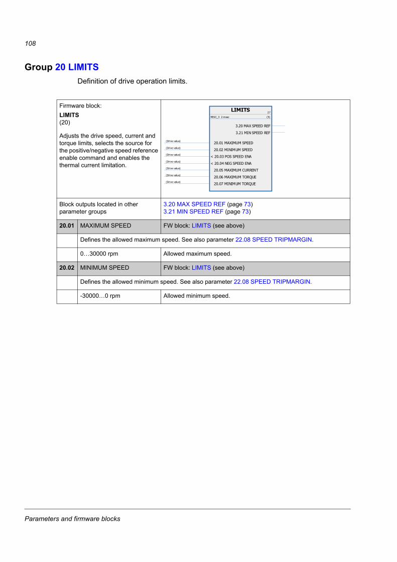
108
Group 20 LIMITSDefinition of drive operation limits.
20Firmware block:LIMITS(20)
Adjusts the drive speed, current and torque limits, selects the source for the positive/negative speed reference enable command and enables the thermal current limitation.
Block outputs located in other parameter groups
3.20 MAX SPEED REF (page 73)3.21 MIN SPEED REF (page 73)
20.01 MAXIMUM SPEED FW block: LIMITS (see above)
Defines the allowed maximum speed. See also parameter 22.08 SPEED TRIPMARGIN.
0…30000 rpm Allowed maximum speed.
20.02 MINIMUM SPEED FW block: LIMITS (see above)
Defines the allowed minimum speed. See also parameter 22.08 SPEED TRIPMARGIN.
-30000…0 rpm Allowed minimum speed.
LIMITS 27
MISC_3 2 msec (5)
20.01 MAXIMUM SPEED(Drive value)
20.02 MINIMUM SPEED(Drive value)
< 20.03 POS SPEED ENA(Drive value)
< 20.04 NEG SPEED ENA(Drive value)
20.05 MAXIMUM CURRENT(Drive value)
20.06 MAXIMUM TORQUE(Drive value)
20.07 MINIMUM TORQUE(Drive value)
3.20 MAX SPEED REF
3.21 MIN SPEED REF
Parameters and firmware blocks
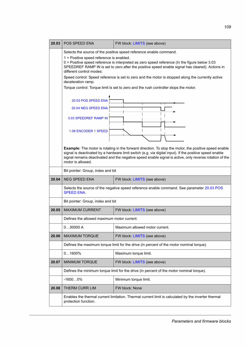
109
20.03 POS SPEED ENA FW block: LIMITS (see above)
Selects the source of the positive speed reference enable command.1 = Positive speed reference is enabled.0 = Positive speed reference is interpreted as zero speed reference (In the figure below 3.03 SPEEDREF RAMP IN is set to zero after the positive speed enable signal has cleared). Actions in different control modes:Speed control: Speed reference is set to zero and the motor is stopped along the currently active deceleration ramp.Torque control: Torque limit is set to zero and the rush controller stops the motor.
Example: The motor is rotating in the forward direction. To stop the motor, the positive speed enable signal is deactivated by a hardware limit switch (e.g. via digital input). If the positive speed enable signal remains deactivated and the negative speed enable signal is active, only reverse rotation of the motor is allowed.
Bit pointer: Group, index and bit
20.04 NEG SPEED ENA FW block: LIMITS (see above)
Selects the source of the negative speed reference enable command. See parameter 20.03 POS SPEED ENA.
Bit pointer: Group, index and bit
20.05 MAXIMUM CURRENT FW block: LIMITS (see above)
Defines the allowed maximum motor current.
0…30000 A Maximum allowed motor current.
20.06 MAXIMUM TORQUE FW block: LIMITS (see above)
Defines the maximum torque limit for the drive (in percent of the motor nominal torque).
0…1600% Maximum torque limit.
20.07 MINIMUM TORQUE FW block: LIMITS (see above)
Defines the minimum torque limit for the drive (in percent of the motor nominal torque).
-1600…0% Minimum torque limit.
20.08 THERM CURR LIM FW block: None
Enables the thermal current limitation. Thermal current limit is calculated by the inverter thermal protection function.
20.03 POS SPEED ENA
20.04 NEG SPEED ENA
3.03 SPEEDREF RAMP IN
1.08 ENCODER 1 SPEED
Parameters and firmware blocks
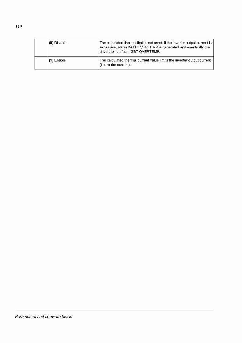
110
(0) Disable The calculated thermal limit is not used. If the inverter output current is excessive, alarm IGBT OVERTEMP is generated and eventually the drive trips on fault IGBT OVERTEMP.
(1) Enable The calculated thermal current value limits the inverter output current (i.e. motor current).
Parameters and firmware blocks
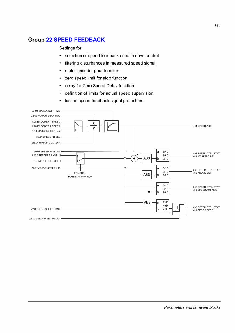
111
Group 22 SPEED FEEDBACKSettings for
• selection of speed feedback used in drive control
• filtering disturbances in measured speed signal
• motor encoder gear function
• zero speed limit for stop function
• delay for Zero Speed Delay function
• definition of limits for actual speed supervision
• loss of speed feedback signal protection.
xy
22.04 MOTOR GEAR DIV
22.03 MOTOR GEAR MUL
22.02 SPEED ACT FTIME
22.01 SPEED FB SEL
1.14 SPEED ESTIMATED
22.05 ZERO SPEED LIMIT
1.08 ENCODER 1 SPEED
1.10 ENCODER 2 SPEED 1.01 SPEED ACT
22.06 ZERO SPEED DELAY
a
b
a>ba=ba<b t 6.03 SPEED CTRL STAT
bit 1 ZERO SPEED
6.03 SPEED CTRL STATbit 0 SPEED ACT NEG
ABS
ABS
6.03 SPEED CTRL STATbit 2 ABOVE LIMIT
6.03 SPEED CTRL STATbit 3 AT SETPOINT
0
22.07 ABOVE SPEED LIM
3.03 SPEEDREF RAMP IN26.07 SPEED WINDOW
+-
a
b
a>ba=ba<b
a
b
a>ba=ba<b
a
b
a>ba=ba<b
ABS
3.05 SPEEDREF USED
OPMODE = POSITION SYNCRON
Parameters and firmware blocks
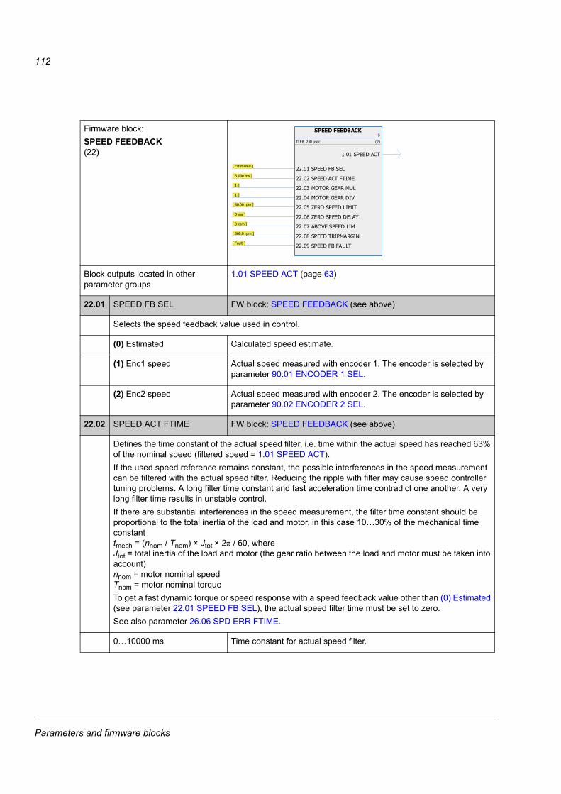
112
22Firmware block:SPEED FEEDBACK(22)
Block outputs located in other parameter groups
1.01 SPEED ACT (page 63)
22.01 SPEED FB SEL FW block: SPEED FEEDBACK (see above)
Selects the speed feedback value used in control.
(0) Estimated Calculated speed estimate.
(1) Enc1 speed Actual speed measured with encoder 1. The encoder is selected by parameter 90.01 ENCODER 1 SEL.
(2) Enc2 speed Actual speed measured with encoder 2. The encoder is selected by parameter 90.02 ENCODER 2 SEL.
22.02 SPEED ACT FTIME FW block: SPEED FEEDBACK (see above)
Defines the time constant of the actual speed filter, i.e. time within the actual speed has reached 63% of the nominal speed (filtered speed = 1.01 SPEED ACT).If the used speed reference remains constant, the possible interferences in the speed measurement can be filtered with the actual speed filter. Reducing the ripple with filter may cause speed controller tuning problems. A long filter time constant and fast acceleration time contradict one another. A very long filter time results in unstable control.If there are substantial interferences in the speed measurement, the filter time constant should be proportional to the total inertia of the load and motor, in this case 10…30% of the mechanical time constant tmech = (nnom / Tnom) × Jtot × 2π / 60, whereJtot = total inertia of the load and motor (the gear ratio between the load and motor must be taken into account)nnom = motor nominal speedTnom = motor nominal torqueTo get a fast dynamic torque or speed response with a speed feedback value other than (0) Estimated (see parameter 22.01 SPEED FB SEL), the actual speed filter time must be set to zero.See also parameter 26.06 SPD ERR FTIME.
0…10000 ms Time constant for actual speed filter.
SPEED FEEDBACK5
TLF8 250 μsec (2)
22.01 SPEED FB SEL [ Estimated ]
22.02 SPEED ACT FTIME [ 3.000 ms ]
22.03 MOTOR GEAR MUL [ 1 ]
22.04 MOTOR GEAR DIV [ 1 ]
22.05 ZERO SPEED LIMIT [ 30.00 rpm ]
22.06 ZERO SPEED DELAY [ 0 ms ]
22.07 ABOVE SPEED LIM [ 0 rpm ]
22.08 SPEED TRIPMARGIN [ 500.0 rpm ]
22.09 SPEED FB FAULT [ Fault ]
1.01 SPEED ACT
Parameters and firmware blocks
113
22.03 MOTOR GEAR MUL FW block: SPEED FEEDBACK (see above)
Defines the motor gear numerator for the motor encoder gear function.
where input speed is encoder 1/2 speed (1.08 ENCODER 1 SPEED / 1.10 ENCODER 2 SPEED) or speed estimate (1.14 SPEED ESTIMATED).Note: If the motor gear ratio differs from 1, the motor model uses an estimated speed instead of the speed feedback value.See also section Motor encoder gear function on page 51.
-231… 231 -1 Numerator for motor encoder gear. Note: A setting of 0 is changed internally to 1.
22.04 MOTOR GEAR DIV FW block: SPEED FEEDBACK (see above)
Defines the motor gear denominator for the motor encoder gear function. See parameter 22.03 MOTOR GEAR MUL.
1 … 231 -1 Denominator for motor encoder gear.
22.05 ZERO SPEED LIMIT FW block: SPEED FEEDBACK (see above)
Defines the zero speed limit. The motor is stopped along a speed ramp until the defined zero speed limit is reached. After the limit, the motor coasts to stop.Note: Too low a setting may result in the drive not stopping at all.
0…30000 rpm Zero speed limit.
22.03 MOTOR GEAR MUL22.04 MOTOR GEAR DIV ------------------------------------------------------------------------ Actual speed
Input speed ----------------------------------=
Parameters and firmware blocks
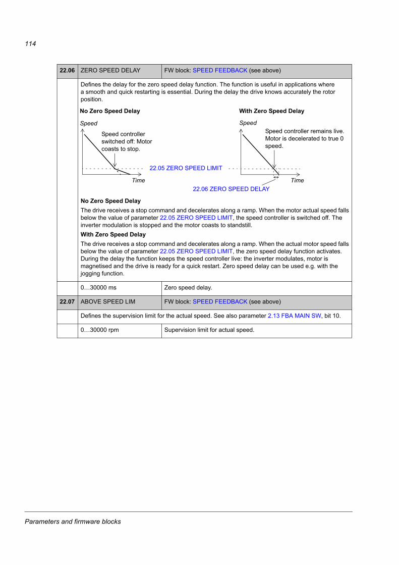
114
22.06 ZERO SPEED DELAY FW block: SPEED FEEDBACK (see above)
Defines the delay for the zero speed delay function. The function is useful in applications where a smooth and quick restarting is essential. During the delay the drive knows accurately the rotor position.
No Zero Speed DelayThe drive receives a stop command and decelerates along a ramp. When the motor actual speed falls below the value of parameter 22.05 ZERO SPEED LIMIT, the speed controller is switched off. The inverter modulation is stopped and the motor coasts to standstill.With Zero Speed DelayThe drive receives a stop command and decelerates along a ramp. When the actual motor speed falls below the value of parameter 22.05 ZERO SPEED LIMIT, the zero speed delay function activates. During the delay the function keeps the speed controller live: the inverter modulates, motor is magnetised and the drive is ready for a quick restart. Zero speed delay can be used e.g. with the jogging function.
0…30000 ms Zero speed delay.
22.07 ABOVE SPEED LIM FW block: SPEED FEEDBACK (see above)
Defines the supervision limit for the actual speed. See also parameter 2.13 FBA MAIN SW, bit 10.
0…30000 rpm Supervision limit for actual speed.
Speed controller switched off: Motor coasts to stop.
Speed controller remains live. Motor is decelerated to true 0 speed.
No Zero Speed Delay With Zero Speed Delay
Speed Speed
22.05 ZERO SPEED LIMIT
22.06 ZERO SPEED DELAYTime Time
Parameters and firmware blocks
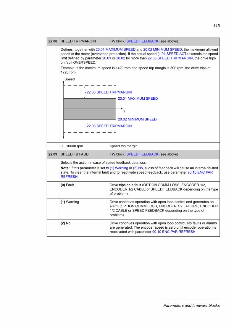
115
22.08 SPEED TRIPMARGIN FW block: SPEED FEEDBACK (see above)
Defines, together with 20.01 MAXIMUM SPEED and 20.02 MINIMUM SPEED, the maximum allowed speed of the motor (overspeed protection). If the actual speed (1.01 SPEED ACT) exceeds the speed limit defined by parameter 20.01 or 20.02 by more than 22.08 SPEED TRIPMARGIN, the drive trips on fault OVERSPEED.Example: If the maximum speed is 1420 rpm and speed trip margin is 300 rpm, the drive trips at 1720 rpm.
0…10000 rpm Speed trip margin.
22.09 SPEED FB FAULT FW block: SPEED FEEDBACK (see above)
Selects the action in case of speed feedback data loss.Note: If this parameter is set to (1) Warning or (2) No, a loss of feedback will cause an internal faulted state. To clear the internal fault and to reactivate speed feedback, use parameter 90.10 ENC PAR REFRESH.
(0) Fault Drive trips on a fault (OPTION COMM LOSS, ENCODER 1/2, ENCODER 1/2 CABLE or SPEED FEEDBACK depending on the type of problem).
(1) Warning Drive continues operation with open loop control and generates an alarm (OPTION COMM LOSS, ENCODER 1/2 FAILURE, ENCODER 1/2 CABLE or SPEED FEEDBACK depending on the type of problem).
(2) No Drive continues operation with open loop control. No faults or alarms are generated. The encoder speed is zero until encoder operation is reactivated with parameter 90.10 ENC PAR REFRESH.
t
20.01 MAXIMUM SPEED
20.02 MINIMUM SPEED
22.08 SPEED TRIPMARGIN
22.08 SPEED TRIPMARGIN
Speed
Parameters and firmware blocks
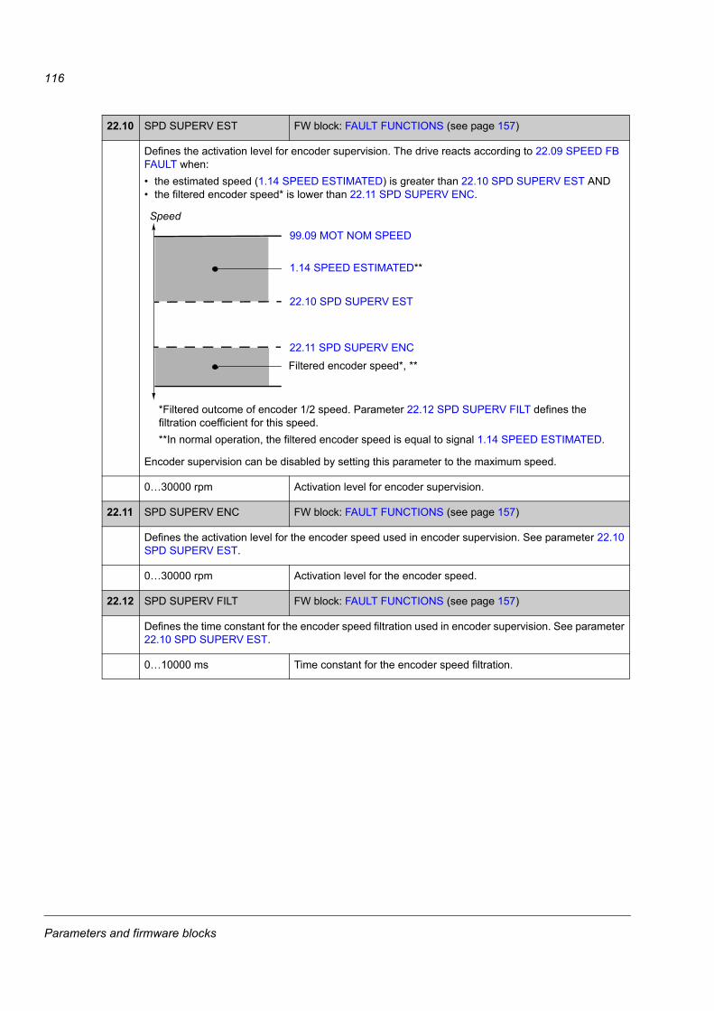
116
22.10 SPD SUPERV EST FW block: FAULT FUNCTIONS (see page 157)
Defines the activation level for encoder supervision. The drive reacts according to 22.09 SPEED FB FAULT when:• the estimated speed (1.14 SPEED ESTIMATED) is greater than 22.10 SPD SUPERV EST AND• the filtered encoder speed* is lower than 22.11 SPD SUPERV ENC.
Encoder supervision can be disabled by setting this parameter to the maximum speed.
0…30000 rpm Activation level for encoder supervision.
22.11 SPD SUPERV ENC FW block: FAULT FUNCTIONS (see page 157)
Defines the activation level for the encoder speed used in encoder supervision. See parameter 22.10 SPD SUPERV EST.
0…30000 rpm Activation level for the encoder speed.
22.12 SPD SUPERV FILT FW block: FAULT FUNCTIONS (see page 157)
Defines the time constant for the encoder speed filtration used in encoder supervision. See parameter 22.10 SPD SUPERV EST.
0…10000 ms Time constant for the encoder speed filtration.
1.14 SPEED ESTIMATED**
Speed
22.10 SPD SUPERV EST
99.09 MOT NOM SPEED
22.11 SPD SUPERV ENC
Filtered encoder speed*, **
*Filtered outcome of encoder 1/2 speed. Parameter 22.12 SPD SUPERV FILT defines the filtration coefficient for this speed.**In normal operation, the filtered encoder speed is equal to signal 1.14 SPEED ESTIMATED.
Parameters and firmware blocks
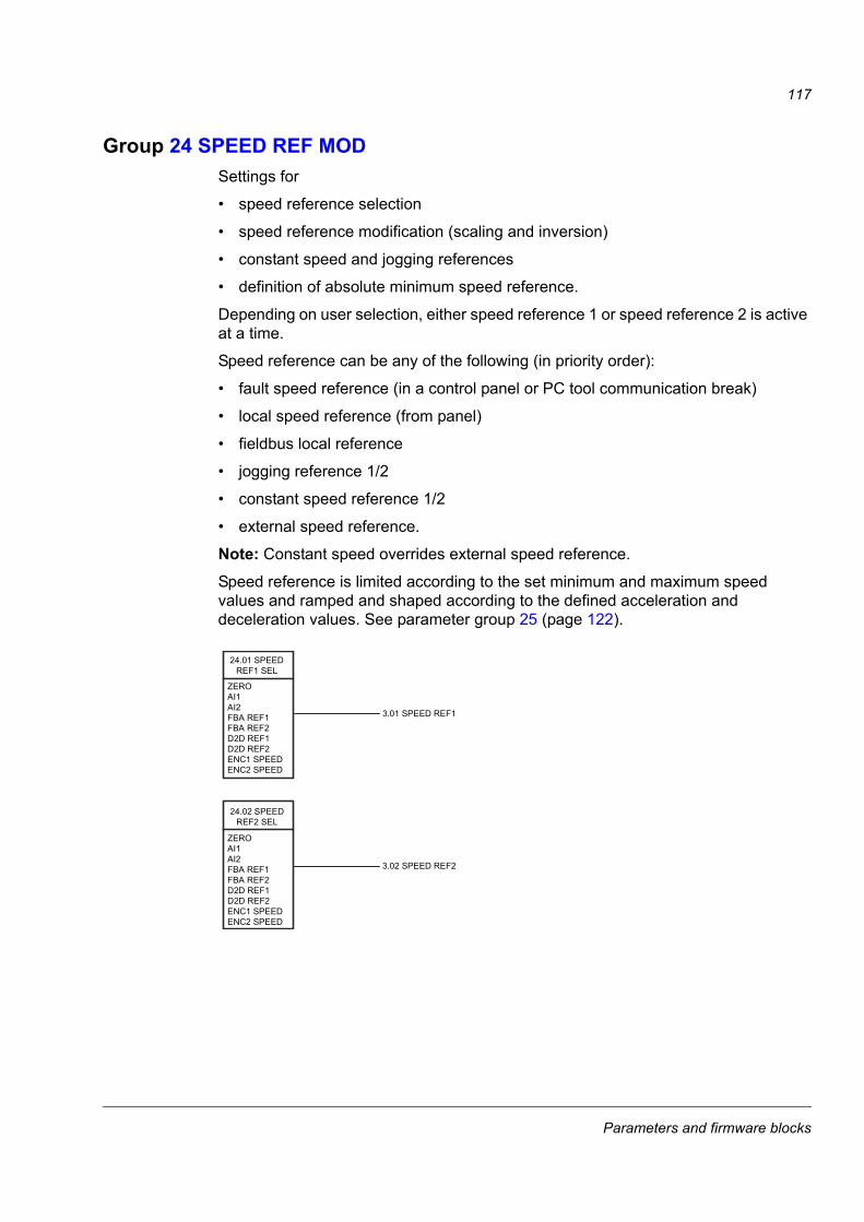
117
Group 24 SPEED REF MODSettings for
• speed reference selection
• speed reference modification (scaling and inversion)
• constant speed and jogging references
• definition of absolute minimum speed reference.
Depending on user selection, either speed reference 1 or speed reference 2 is active at a time.
Speed reference can be any of the following (in priority order):
• fault speed reference (in a control panel or PC tool communication break)
• local speed reference (from panel)
• fieldbus local reference
• jogging reference 1/2
• constant speed reference 1/2
• external speed reference.
Note: Constant speed overrides external speed reference.
Speed reference is limited according to the set minimum and maximum speed values and ramped and shaped according to the defined acceleration and deceleration values. See parameter group 25 (page 122).
3.01 SPEED REF1
3.02 SPEED REF2
ZEROAI1AI2FBA REF1FBA REF2D2D REF1D2D REF2ENC1 SPEEDENC2 SPEED
24.01 SPEED REF1 SEL
ZEROAI1AI2FBA REF1FBA REF2D2D REF1D2D REF2ENC1 SPEEDENC2 SPEED
24.02 SPEED REF2 SEL
Parameters and firmware blocks

118
24Firmware block:SPEED REF SEL(23)
Selects the sources for two speed references, REF1 or REF2, from a selection list. Also shows the values of both speed references.The sources can alternatively be selected with value pointer parameters. See firmware block SPEED REF MOD on page 119.
Block outputs located in other parameter groups
3.01 SPEED REF1 (page 72)3.02 SPEED REF2 (page 72)
24.01 SPEED REF1 SEL FW block: SPEED REF SEL (see above)
Selects the source for speed reference 1 (3.01 SPEED REF1).Source for speed reference 1/2 can also be selected by value pointer parameter 24.03 SPEED REF1 IN / 24.04 SPEED REF2 IN.
(0) ZERO Zero reference.
(1) AI1 Analogue input AI1.
(2) AI2 Analogue input AI2.
(3) FBA REF1 Fieldbus reference 1.
(4) FBA REF2 Fieldbus reference 2.
(5) D2D REF1 Drive to drive reference 1.
03.03 SPEEDREF RAMP IN
3.01 SPEED REF1
3.02 SPEED REF2
24.05 SPEED REF 1/2 SEL
24.06 SPEED SHARE
24.07 SPEEDREF NEG ENA
1
-1
24.09 CONST SPEED ENA
24.10 SPEED REF JOG1
24.11 SPEED REF JOG2
10.13 FB CW USEDbit 10 JOGGING
06.02 STATUS WORD 2bit 5 JOGGING
24.08 CONST SPEED
x
x
20.03 POS SPEED ENA
0
20.02 MINIMUM SPEED
20.04 NEG SPEED ENA
0
06.02 STATUS WORD 2 bit 12 RAMP IN 0
Local speed reference
06.01 STATUS WORD 1 bit 11 LOCAL PANEL
46.02 SPEED REF SAFE
SAFE SPEED COMMAND
06.01 STATUS WORD 1 bit 9 LOCAL FB
0
20.01 MAXIMUM SPEED
2.14 FBA MAIN REF1
24.12 SPEED REF MIN ABS
SPEED REF SEL3
TLF2 500 μsec (1)
24.01 SPEED REF1 SEL [ AI1 ]
24.02 SPEED REF2 SEL [ ZERO ]
3.01 SPEED REF1
3.02 SPEED REF2
Parameters and firmware blocks

119
(6) D2D REF2 Drive to drive reference 2.
(7) ENC1 SPEED Encoder 1 (1.08 ENCODER 1 SPEED).
(8) ENC2 SPEED Encoder 2 (1.10 ENCODER 2 SPEED).
24.02 SPEED REF2 SEL FW block: SPEED REF SEL (see above)
Selects the source for speed reference 2 (3.02 SPEED REF2).See parameter 24.01 SPEED REF1 SEL.
Firmware block:SPEED REF MOD(24)
This block• selects the sources for two speed
references, REF1 or REF2• scales and inverts the speed
reference• defines the constant speed
reference• defines the speed reference for
jogging functions 1 and 2• defines the speed reference
absolute minimum limit.
Block outputs located in other parameter groups
3.03 SPEEDREF RAMP IN (page 72)
24.03 SPEED REF1 IN FW block: SPEED REF MOD (see above)
Selects the source for speed reference 1 (overrides the setting of parameter 24.01 SPEED REF1 SEL). The default value is P.3.1, i.e. 3.01 SPEED REF1, which is the output of the SPEED REF RAMP block.
Value pointer: Group and index
24.04 SPEED REF2 IN FW block: SPEED REF MOD (see above)
Selects the source for speed reference 2 (overrides the setting of parameter 24.02 SPEED REF2 SEL). The default value is P.3.2, i.e. 3.02 SPEED REF2, which is the output of the SPEED REF RAMP block.
Value pointer: Group and index
24.05 SPEED REF 1/2SEL FW block: SPEED REF MOD (see above)
Selects between speed reference 1 or 2. Reference 1/2 source is defined by parameter 24.03 SPEED REF1 IN / 24.04 SPEED REF2 IN. 0 = Speed reference 1.
Bit pointer: Group, index and bit
24.06 SPEED SHARE FW block: SPEED REF MOD (see above)
Defines the scaling factor for speed reference 1/2 (speed reference 1 or 2 is multiplied by the defined value). Speed reference 1 or 2 is selected by parameter 24.05 SPEED REF 1/2SEL.
SPEED REF MOD4
TLF2 500 μsec (2)
< 24.03 SPEED REF1 IN [ AI1 SCALED ](3 / 2.05)
< 24.04 SPEED REF2 IN [ SPEED REF2 ](6 / 3.02)
< 24.05 SPEED REF 1/2SEL [ FALSE ]
24.06 SPEED SHARE [ 1.000 ]
< 24.07 SPEEDREF NEG ENA [ FALSE ]
24.08 CONST SPEED [ 0 rpm ]
< 24.09 CONST SPEED ENA [ FALSE ]
24.10 SPEED REF JOG1 [ 0 rpm ]
24.11 SPEED REF JOG2 [ 0 rpm ]
24.12 SPEED REFMIN ABS [ 0 rpm ]
3.03 SPEEDREF RAMP IN
Parameters and firmware blocks
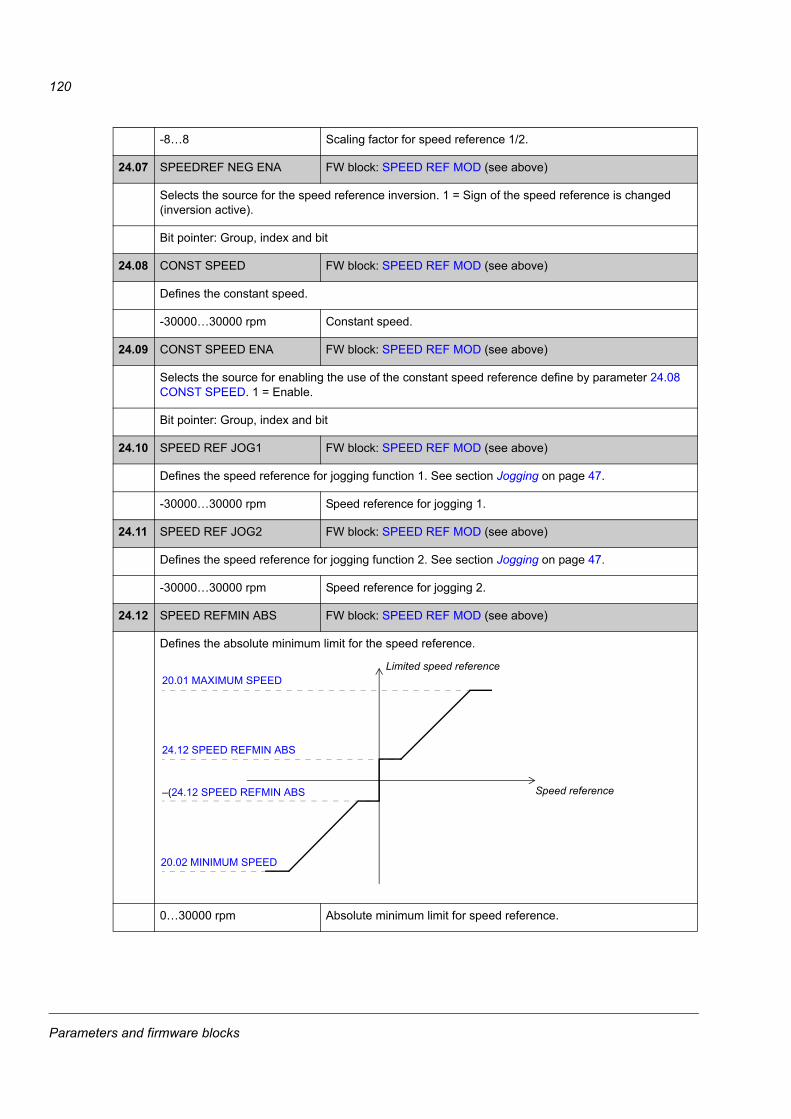
120
-8…8 Scaling factor for speed reference 1/2.
24.07 SPEEDREF NEG ENA FW block: SPEED REF MOD (see above)
Selects the source for the speed reference inversion. 1 = Sign of the speed reference is changed (inversion active).
Bit pointer: Group, index and bit
24.08 CONST SPEED FW block: SPEED REF MOD (see above)
Defines the constant speed.
-30000…30000 rpm Constant speed.
24.09 CONST SPEED ENA FW block: SPEED REF MOD (see above)
Selects the source for enabling the use of the constant speed reference define by parameter 24.08 CONST SPEED. 1 = Enable.
Bit pointer: Group, index and bit
24.10 SPEED REF JOG1 FW block: SPEED REF MOD (see above)
Defines the speed reference for jogging function 1. See section Jogging on page 47.
-30000…30000 rpm Speed reference for jogging 1.
24.11 SPEED REF JOG2 FW block: SPEED REF MOD (see above)
Defines the speed reference for jogging function 2. See section Jogging on page 47.
-30000…30000 rpm Speed reference for jogging 2.
24.12 SPEED REFMIN ABS FW block: SPEED REF MOD (see above)
Defines the absolute minimum limit for the speed reference.
0…30000 rpm Absolute minimum limit for speed reference.
Limited speed reference
Speed reference
20.01 MAXIMUM SPEED
–(24.12 SPEED REFMIN ABS
24.12 SPEED REFMIN ABS
20.02 MINIMUM SPEED
Parameters and firmware blocks
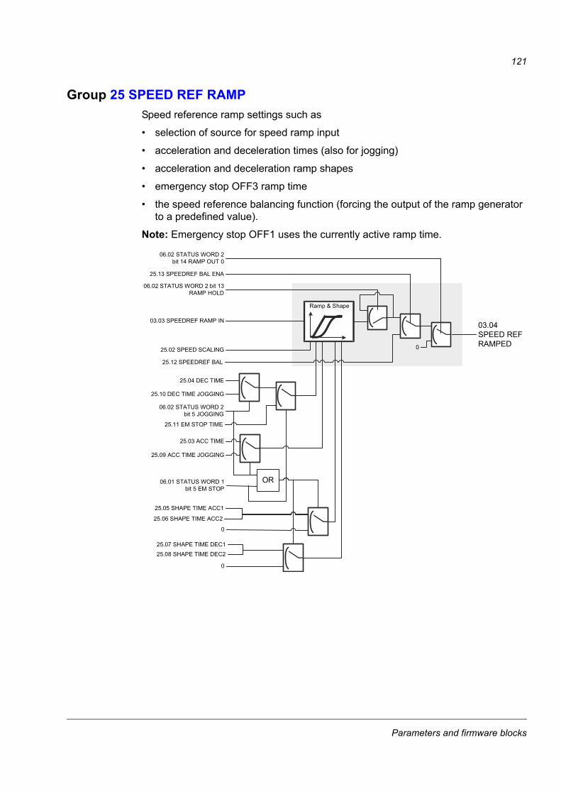
121
Group 25 SPEED REF RAMPSpeed reference ramp settings such as
• selection of source for speed ramp input
• acceleration and deceleration times (also for jogging)
• acceleration and deceleration ramp shapes
• emergency stop OFF3 ramp time
• the speed reference balancing function (forcing the output of the ramp generator to a predefined value).
Note: Emergency stop OFF1 uses the currently active ramp time.
0
Ramp & Shape
03.03 SPEEDREF RAMP IN
25.02 SPEED SCALING
25.03 ACC TIME
25.04 DEC TIME
25.05 SHAPE TIME ACC1
25.06 SHAPE TIME ACC2
25.07 SHAPE TIME DEC125.08 SHAPE TIME DEC2
25.10 DEC TIME JOGGING
25.11 EM STOP TIME
25.12 SPEEDREF BAL
25.13 SPEEDREF BAL ENA
25.09 ACC TIME JOGGING
0
06.01 STATUS WORD 1 bit 5 EM STOP
06.02 STATUS WORD 2bit 5 JOGGING
OR
06.02 STATUS WORD 2 bit 14 RAMP OUT 0
06.02 STATUS WORD 2 bit 13 RAMP HOLD
0
03.04 SPEED REF RAMPED
Parameters and firmware blocks
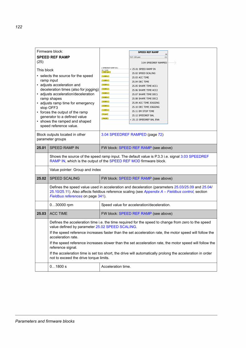
122
25Firmware block:SPEED REF RAMP(25)
This block• selects the source for the speed
ramp input• adjusts acceleration and
deceleration times (also for jogging)• adjusts acceleration/deceleration
ramp shapes• adjusts ramp time for emergency
stop OFF3• forces the output of the ramp
generator to a defined value• shows the ramped and shaped
speed reference value.
Block outputs located in other parameter groups
3.04 SPEEDREF RAMPED (page 72)
25.01 SPEED RAMP IN FW block: SPEED REF RAMP (see above)
Shows the source of the speed ramp input. The default value is P.3.3 i.e. signal 3.03 SPEEDREF RAMP IN, which is the output of the SPEED REF MOD firmware block.
Value pointer: Group and index
25.02 SPEED SCALING FW block: SPEED REF RAMP (see above)
Defines the speed value used in acceleration and deceleration (parameters 25.03/25.09 and 25.04/25.10/25.11). Also affects fieldbus reference scaling (see Appendix A – Fieldbus control, section Fieldbus references on page 341).
0…30000 rpm Speed value for acceleration/deceleration.
25.03 ACC TIME FW block: SPEED REF RAMP (see above)
Defines the acceleration time i.e. the time required for the speed to change from zero to the speed value defined by parameter 25.02 SPEED SCALING.If the speed reference increases faster than the set acceleration rate, the motor speed will follow the acceleration rate.If the speed reference increases slower than the set acceleration rate, the motor speed will follow the reference signal.If the acceleration time is set too short, the drive will automatically prolong the acceleration in order not to exceed the drive torque limits.
0…1800 s Acceleration time.
SPEED REF RAMP28
TLF3 250 μsec (1)
< 25.01 SPEED RAMP IN[ SPEEDREF RAMP IN ](6 / 3.03)
25.02 SPEED SCALING [ 1500 rpm ]
25.03 ACC TIME [ 1.000 s ]
25.04 DEC TIME [ 1.000 s ]
25.05 SHAPE TIME ACC1 [ 0.000 s ]
25.06 SHAPE TIME ACC2 [ 0.000 s ]
25.07 SHAPE TIME DEC1 [ 0.000 s ]
25.08 SHAPE TIME DEC2 [ 0.000 s ]
25.09 ACC TIME JOGGING [ 0.000 s ]
25.10 DEC TIME JOGGING [ 0.000 s ]
25.11 EM STOP TIME [ 1.000 s ]
25.12 SPEEDREF BAL [ 0 rpm ]
< 25.13 SPEEDREF BAL ENA [ FALSE ]
3.04 SPEEDREF RAMPED
Parameters and firmware blocks

123
25.04 DEC TIME FW block: SPEED REF RAMP (see above)
Defines the deceleration time i.e. the time required for the speed to change from the speed value defined by parameter 25.02 SPEED SCALING to zero.If the speed reference decreases slower than the set deceleration rate, the motor speed will follow the reference signal.If the reference changes faster than the set deceleration rate, the motor speed will follow the deceleration rate.If the deceleration time is set too short, the drive will automatically prolong the deceleration in order not to exceed drive torque limits. If there is any doubt about the deceleration time being too short, ensure that the DC overvoltage control is on (parameter 47.01 OVERVOLTAGE CTRL).Note: If a short deceleration time is needed for a high inertia application, the drive should be equipped with an electric braking option e.g. with a brake chopper (built-in) and a brake resistor.
0…1800 s Deceleration time.
25.05 SHAPE TIME ACC1 FW block: SPEED REF RAMP (see above)
Selects the shape of the acceleration ramp at the beginning of the acceleration.0.00 s: Linear ramp. Suitable for steady acceleration or deceleration and for slow ramps.0.01…1000.00 s: S-curve ramp. S-curve ramps are ideal for conveyor and lifting applications. The S-curve consists of symmetrical curves at both ends of the ramp and a linear part in between.Note: When jogging or emergency ramp stop is active, acceleration and deceleration shape times are forced to zero.
0…1000 s Ramp shape at beginning of acceleration.
25.06 SHAPE TIME ACC2 FW block: SPEED REF RAMP (see above)
Selects the shape of the acceleration ramp at the end of the acceleration. See parameter 25.05 SHAPE TIME ACC1.
0…1000 s Ramp shape at end of acceleration.
25.07 SHAPE TIME DEC1 FW block: SPEED REF RAMP (see above)
Selects the shape of the deceleration ramp at the beginning of the deceleration. See parameter 25.05 SHAPE TIME ACC1.
0…1000 s Ramp shape at beginning of deceleration.
S-curve ramp: Par. 25.06 > 0 s
Linear ramp: Par. 25.05 = 0 s
Linear ramp: Par. 25.06 = 0 s
S-curve ramp: Par. 25.05 > 0 s
S-curve ramp: Par. 25.07 > 0 s
Linear ramp: Par. 25.08 = 0 s
S-curve ramp:Par. 25.08 > 0 s
Speed
Time
Speed
Linear ramp: Par. 25.07 = 0 s
Time
Parameters and firmware blocks
124
25.08 SHAPE TIME DEC2 FW block: SPEED REF RAMP (see above)
Selects the shape of the deceleration ramp at the end of the deceleration. See parameter 25.05 SHAPE TIME ACC1.
0…1000 s Ramp shape at end of deceleration.
25.09 ACC TIME JOGGING FW block: SPEED REF RAMP (see above)
Defines the acceleration time for the jogging function i.e. the time required for the speed to change from zero to the speed value defined by parameter 25.02 SPEED SCALING.
0…1800 s Acceleration time for jogging.
25.10 DEC TIME JOGGING FW block: SPEED REF RAMP (see above)
Defines the deceleration time for the jogging function i.e. the time required for the speed to change from the speed value defined by parameter 25.02 SPEED SCALING to zero.
0…1800 s Deceleration time for jogging.
25.11 EM STOP TIME FW block: SPEED REF RAMP (see above)
Defines the time inside which the drive is stopped if an emergency stop OFF3 is activated (i.e. the time required for the speed to change from the speed value defined by parameter 25.02 SPEED SCALING to zero). Emergency stop activation source is selected by parameter 10.10 EM STOP OFF3. Emergency stop can also be activated through fieldbus (2.12 FBA MAIN CW).Emergency stop OFF1 uses the active ramp time.
0…1800 s Emergency stop OFF3 deceleration time.
25.12 SPEEDREF BAL FW block: SPEED REF RAMP (see above)
Defines the reference for the speed ramp balancing, i.e. the output of the speed reference ramp firmware block is forced to a defined value.The source for the balancing enable signal is selected by parameter 25.13 SPEEDREF BAL.
-30000…30000 rpm Speed ramp balancing reference.
25.13 SPEEDREF BAL ENA FW block: SPEED REF RAMP (see above)
Selects the source for enabling the speed ramp balancing. See parameter 25.12 SPEEDREF BAL. 1 = Speed ramp balancing enabled.
Bit pointer: Group, index and bit
Parameters and firmware blocks
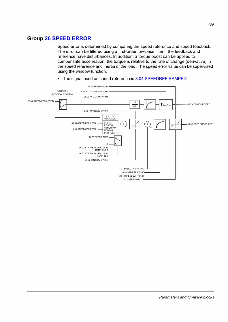
125
Group 26 SPEED ERRORSpeed error is determined by comparing the speed reference and speed feedback. The error can be filtered using a first-order low-pass filter if the feedback and reference have disturbances. In addition, a torque boost can be applied to compensate acceleration; the torque is relative to the rate of change (derivative) in the speed reference and inertia of the load. The speed error value can be supervised using the window function.
• The signal used as speed reference is 3.04 SPEEDREF RAMPED.
26.05 SPEED STEP
26.06 SPD ERR FTIME
20.01 MAXIMUM SPEED
20.02 MINIMUM SPEED
TAccCom
26.08 ACC COMP DER TIME
26.09 ACC COMP FTIME
ddt
006.02 STATUS WORD 2 bit 14
RAMP OUT 006.02 STATUS WORD 2 bit 12
RAMP IN 0
+-
26.10 SPEED WIN FUNC
26.11 SPEED WIN HI
26.12 SPEED WIN LO
4.01 SPEED REF PCTRL
26.04 SPEED FEED PCTRL
1.01 SPEED ACT NCTRL
OPMODE = POSITION SYNCRON
03.04 SPEED REF NCTRL SPEEDPOSITIONSYNCHRONHOMINGPROF VEL
6.12 OP MODE ACK
+ 3.06 SPEED ERROR FILT
3.07 ACC COMP TORQ
Parameters and firmware blocks
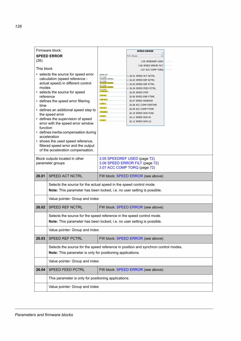
126
26Firmware block:SPEED ERROR(26)
This block• selects the source for speed error
calculation (speed reference - actual speed) in different control modes
• selects the source for speed reference
• defines the speed error filtering time
• defines an additional speed step to the speed error
• defines the supervision of speed error with the speed error window function
• defines inertia compensation during acceleration
• shows the used speed reference, filtered speed error and the output of the acceleration compensation.
Block outputs located in other parameter groups
3.05 SPEEDREF USED (page 72)3.06 SPEED ERROR FILT (page 72)3.07 ACC COMP TORQ (page 72)
26.01 SPEED ACT NCTRL FW block: SPEED ERROR (see above)
Selects the source for the actual speed in the speed control mode.Note: This parameter has been locked, i.e. no user setting is possible.
Value pointer: Group and index
26.02 SPEED REF NCTRL FW block: SPEED ERROR (see above)
Selects the source for the speed reference in the speed control mode.Note: This parameter has been locked, i.e. no user setting is possible.
Value pointer: Group and index
26.03 SPEED REF PCTRL FW block: SPEED ERROR (see above)
Selects the source for the speed reference in position and synchron control modes.Note: This parameter is only for positioning applications.
Value pointer: Group and index
26.04 SPEED FEED PCTRL FW block: SPEED ERROR (see above)
This parameter is only for positioning applications.
Value pointer: Group and index
SPEED ERROR6
TLF3 250 μsec (2)
< 26.01 SPEED ACT NCTRLSPEED ACT(7 / 1.01)
< 26.02 SPEED REF NCTRLSPEEDREF RAMPED(6 / 3.04)
< 26.03 SPEED REF PCTRLSPEEDREF RAMPED(6 / 3.04)
< 26.04 SPEED FEED PCTRLSPEEDREF RAMPED(6 / 3.04)
26.05 SPEED STEP [ 0.00 rpm ]
26.06 SPEED ERR FTIME [ 0.0 ms ]
26.07 SPEED WINDOW [ 100 rpm ]
26.08 ACC COMP DERTIME [ 0.00 s ]
26.09 ACC COMP FTIME [ 8.0 ms ]
26.10 SPEED WIN FUNC [ Disabled ]
26.11 SPEED WIN HI [ 0 rpm ]
26.12 SPEED WIN LO [ 0 rpm ]
3.05 SPEEDREF USED
3.06 SPEED ERROR FILT
3.07 ACC COMP TORQ
Parameters and firmware blocks
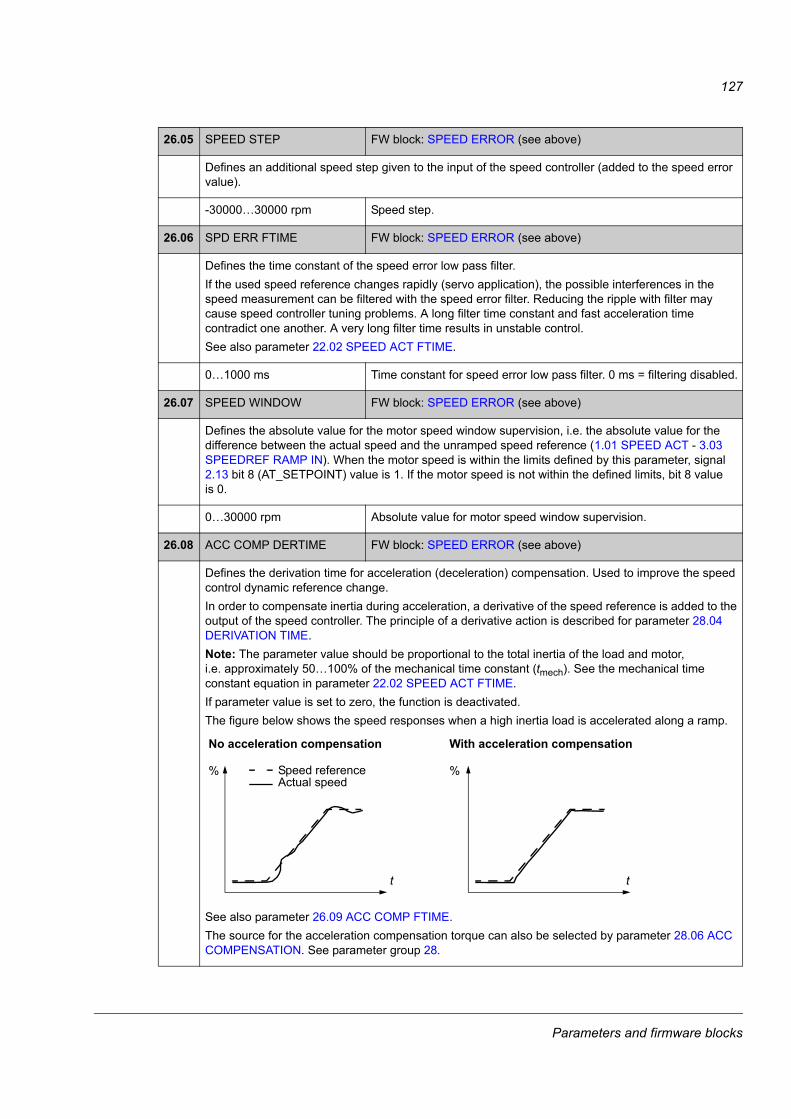
127
26.05 SPEED STEP FW block: SPEED ERROR (see above)
Defines an additional speed step given to the input of the speed controller (added to the speed error value).
-30000…30000 rpm Speed step.
26.06 SPD ERR FTIME FW block: SPEED ERROR (see above)
Defines the time constant of the speed error low pass filter. If the used speed reference changes rapidly (servo application), the possible interferences in the speed measurement can be filtered with the speed error filter. Reducing the ripple with filter may cause speed controller tuning problems. A long filter time constant and fast acceleration time contradict one another. A very long filter time results in unstable control. See also parameter 22.02 SPEED ACT FTIME.
0…1000 ms Time constant for speed error low pass filter. 0 ms = filtering disabled.
26.07 SPEED WINDOW FW block: SPEED ERROR (see above)
Defines the absolute value for the motor speed window supervision, i.e. the absolute value for the difference between the actual speed and the unramped speed reference (1.01 SPEED ACT - 3.03 SPEEDREF RAMP IN). When the motor speed is within the limits defined by this parameter, signal 2.13 bit 8 (AT_SETPOINT) value is 1. If the motor speed is not within the defined limits, bit 8 value is 0.
0…30000 rpm Absolute value for motor speed window supervision.
26.08 ACC COMP DERTIME FW block: SPEED ERROR (see above)
Defines the derivation time for acceleration (deceleration) compensation. Used to improve the speed control dynamic reference change.In order to compensate inertia during acceleration, a derivative of the speed reference is added to the output of the speed controller. The principle of a derivative action is described for parameter 28.04 DERIVATION TIME.Note: The parameter value should be proportional to the total inertia of the load and motor, i.e. approximately 50…100% of the mechanical time constant (tmech). See the mechanical time constant equation in parameter 22.02 SPEED ACT FTIME.If parameter value is set to zero, the function is deactivated.The figure below shows the speed responses when a high inertia load is accelerated along a ramp.
See also parameter 26.09 ACC COMP FTIME.The source for the acceleration compensation torque can also be selected by parameter 28.06 ACC COMPENSATION. See parameter group 28.
tt
% %
No acceleration compensation With acceleration compensation
Speed referenceActual speed
Parameters and firmware blocks
128
0…600 s Derivation time for acceleration/deceleration compensation.
26.09 ACC COMP FTIME FW block: SPEED ERROR (see above)
Defines the filter time for the acceleration compensation.
0…1000 ms Filter time for acceleration compensation. 0 ms = filtering disabled.
26.10 SPEED WIN FUNC FW block: SPEED ERROR (see above)
Enables or disables speed error window control.Speed error window control forms a speed supervision function for a torque-controlled drive. It supervises the speed error value (speed reference – actual speed). In the normal operating range, window control keeps the speed controller input at zero. The speed controller is evoked only if• the speed error exceeds the upper boundary of the window (parameter 26.11 SPEED WIN HI), or• the absolute value of the negative speed error exceeds the lower boundary of the window
(parameter 26.12 SPEED WIN LO).When the speed error moves outside the window, the exceeding part of the error value is connected to the speed controller. The speed controller produces a reference term relative to the input and gain of the speed controller (parameter 28.02 PROPORT GAIN) which the torque selector adds to the torque reference. The result is used as the internal torque reference for the drive.Example: In a load loss condition, the internal torque reference of the drive is decreased to prevent an excessive rise of the motor speed. If window control were inactive, the motor speed would rise until a speed limit of the drive were reached.
(0) Disabled Speed error window control inactive.
(1) Absolute Speed error window control active. The boundaries defined by parameters 26.11 and 26.12 are absolute.
(2) Relative Speed error window control active. The boundaries defined by parameters 26.11 and 26.12 are relative to speed reference.
26.11 SPEED WIN HI FW block: SPEED ERROR (see above)
Defines the upper boundary of the speed error window. Depending on the setting of parameter 26.10 SPEED WIN FUNC, this is either an absolute value or relative to speed reference.
0…3000 rpm Upper boundary of speed error window.
26.12 SPEED WIN LO FW block: SPEED ERROR (see above)
Defines the lower boundary of the speed error window. Depending on the setting of parameter 26.10 SPEED WIN FUNC, this is either an absolute value or relative to speed reference.
0…3000 rpm Lower boundary of speed error window.
Parameters and firmware blocks
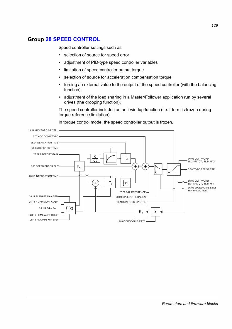
129
Group 28 SPEED CONTROLSpeed controller settings such as
• selection of source for speed error
• adjustment of PID-type speed controller variables
• limitation of speed controller output torque
• selection of source for acceleration compensation torque
• forcing an external value to the output of the speed controller (with the balancing function).
• adjustment of the load sharing in a Master/Follower application run by several drives (the drooping function).
The speed controller includes an anti-windup function (i.e. I-term is frozen during torque reference limitation).
In torque control mode, the speed controller output is frozen.
3.07 ACC COMP TORQ
Kp
Ti
Td
Kp
28.04 DERIVATION TIME
28.05 DERIV FILT TIME
28.02 PROPORT GAIN
28.07 DROOPING RATE
28.08 BAL REFERENCE
28.03 INTEGRATION TIME
3.08 TORQ REF SP CTRL
28.11 MAX TORQ SP CTRL
28.10 MIN TORQ SP CTRL
28.09 SPEEDCTRL BAL EN
+ +
+
ddt
� dt
x
28.14 P GAIN ADPT COEF
28.15 I TIME ADPT COEF
28.12 PI ADAPT MAX SPD
28.13 PI ADAPT MIN SPD
1.01 SPEED ACT F(x)
06.05 LIMIT WORD 1bit 1 SPD CTL TLIM MIN
06.05 LIMIT WORD 1bit 2 SPD CTL TLIM MAX
06.05 SPEED CTRL STATbit 4 BAL ACTIVE
3.06 SPEED ERROR FILT
Parameters and firmware blocks
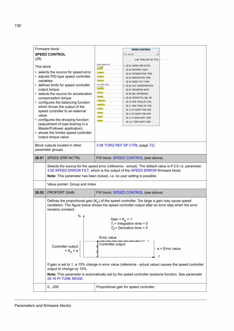
130
28Firmware block:SPEED CONTROL(28)
This block• selects the source for speed error• adjusts PID-type speed controller
variables• defines limits for speed controller
output torque• selects the source for acceleration
compensation torque• configures the balancing function
which forces the output of the speed controller to an external value
• configures the drooping function (adjustment of load sharing in a Master/Follower application)
• shows the limited speed controller output torque value.
Block outputs located in other parameter groups
3.08 TORQ REF SP CTRL (page 72)
28.01 SPEED ERR NCTRL FW block: SPEED CONTROL (see above)
Selects the source for the speed error (reference - actual). The default value is P.3.6 i.e. parameter 3.06 SPEED ERROR FILT, which is the output of the SPEED ERROR firmware block.Note: This parameter has been locked, i.e. no user setting is possible.
Value pointer: Group and index
28.02 PROPORT GAIN FW block: SPEED CONTROL (see above)
Defines the proportional gain (Kp) of the speed controller. Too large a gain may cause speed oscillation. The figure below shows the speed controller output after an error step when the error remains constant.
If gain is set to 1, a 10% change in error value (reference - actual value) causes the speed controller output to change by 10%.Note: This parameter is automatically set by the speed controller autotune function. See parameter 28.16 PI TUNE MODE.
0…200 Proportional gain for speed controller.
SPEED CONTROL7
TLF3 250 μsec (3)
< 28.01 SPEED ERR NCTRLSPEED ERROR FILT(7 / 3.06)
28.02 PROPORT GAIN [ 10.00 ]
28.03 INTEGRATION TIME [ 0.500 s ]
28.04 DERIVATION TIME [ 0.000 s ]
28.05 DERIV FILT TIME [ 8.0 ms ]
< 28.06 ACC COMPENSATIONACC COMP TORQ(7 / 3.07)
28.07 DROOPING RATE [ 0.00 % ]
28.08 BAL REFERENCE [ 0.0 % ]
< 28.09 SPEEDCTRL BAL EN [ FALSE ]
28.10 MIN TORQ SP CTRL [ -300.0 % ]
28.11 MAX TORQ SP CTRL [ 300.0 % ]
28.12 PI ADAPT MAX SPD [ 0 rpm ]
28.13 PI ADAPT MIN SPD [ 0 rpm ]
28.14 P GAIN ADPT COEF [ 1.000 ]
28.15 I TIME ADPT COEF [ 1.000 ]
3.08 TORQ REF SP CTRL
Gain = Kp = 1TI = Integration time = 0TD= Derivation time = 0
t
%
Controller output= Kp × e
Error value
Controller outpute = Error value
Parameters and firmware blocks
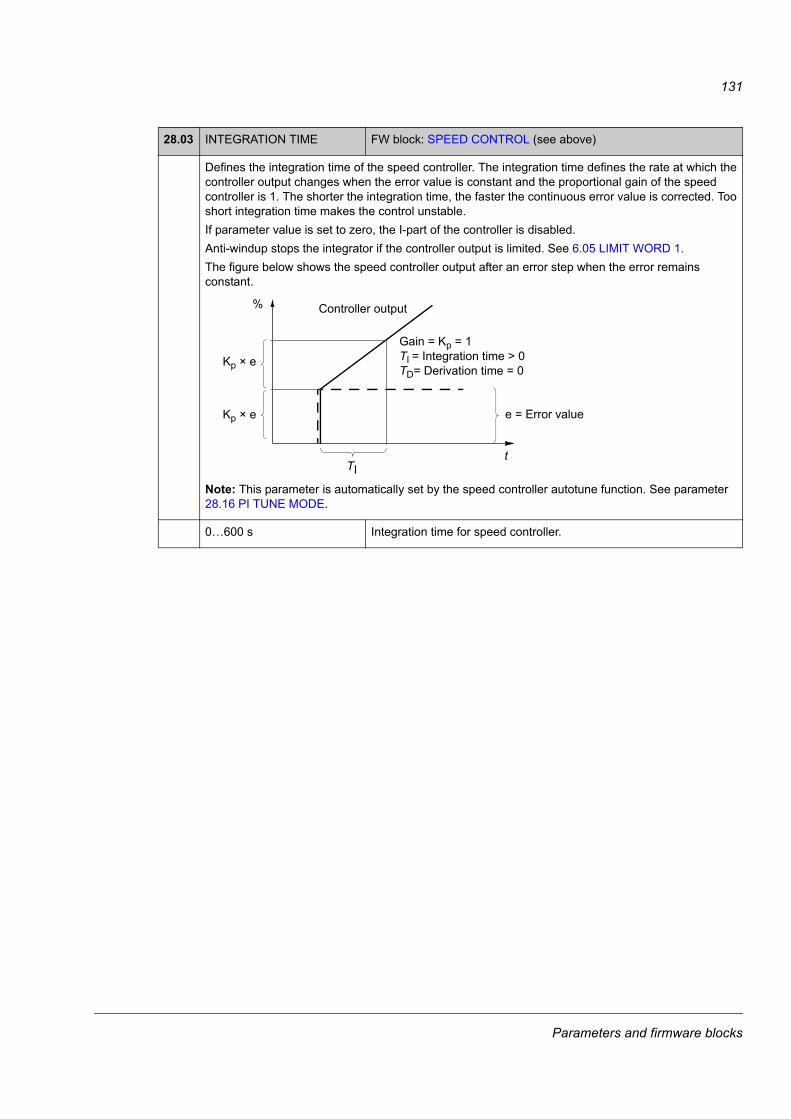
131
28.03 INTEGRATION TIME FW block: SPEED CONTROL (see above)
Defines the integration time of the speed controller. The integration time defines the rate at which the controller output changes when the error value is constant and the proportional gain of the speed controller is 1. The shorter the integration time, the faster the continuous error value is corrected. Too short integration time makes the control unstable.If parameter value is set to zero, the I-part of the controller is disabled.Anti-windup stops the integrator if the controller output is limited. See 6.05 LIMIT WORD 1.The figure below shows the speed controller output after an error step when the error remains constant.
Note: This parameter is automatically set by the speed controller autotune function. See parameter 28.16 PI TUNE MODE.
0…600 s Integration time for speed controller.
TI t
%
Gain = Kp = 1TI = Integration time > 0TD= Derivation time = 0
e = Error value
Controller output
Kp × e
Kp × e
Parameters and firmware blocks

132
28.04 DERIVATION TIME FW block: SPEED CONTROL (see above)
Defines the derivation time of the speed controller. Derivative action boosts the controller output if the error value changes. The longer the derivation time, the more the speed controller output is boosted during the change. If the derivation time is set to zero, the controller works as a PI controller, otherwise as a PID controller. The derivation makes the control more responsive for disturbances.The speed error derivative must be filtered with a low pass filter to eliminate disturbances.The figure below shows the speed controller output after an error step when the error remains constant.
Note: Changing this parameter value is recommended only if a pulse encoder is used.
0…10 s Derivation time for speed controller.
28.05 DERIV FILT TIME FW block: SPEED CONTROL (see above)
Defines the derivation filter time constant.
0…1000 ms Derivation filter time constant.
28.06 ACC COMPENSATION FW block: SPEED CONTROL (see above)
Selects the source for the acceleration compensation torque. The default value is P.3.7, i.e signal 3.07 ACC COMP TORQ, which is the output of the SPEED ERROR firmware block.Note: This parameter has been locked, i.e. no user setting is possible.
Value pointer: Group and index
TI t
%
Gain = Kp = 1TI = Integration time > 0TD= Derivation time > 0Ts= Sample time period = 250 µse = Error valueΔe = Error value change between two samples
Kp × TD × ΔeTs
Controller output
Error value
Kp × e
Kp × e
e = Error value
Parameters and firmware blocks

133
28.07 DROOPING RATE FW block: SPEED CONTROL (see above)
Defines the droop rate (in percent of the motor nominal speed). The drooping slightly decreases the drive speed as the drive load increases. The actual speed decrease at a certain operating point depends on the droop rate setting and the drive load (= torque reference / speed controller output). At 100% speed controller output, drooping is at its nominal level, i.e. equal to the value of this parameter. The drooping effect decreases linearly to zero along with the decreasing load.Drooping rate can be used e.g. to adjust the load sharing in a Master/Follower application run by several drives. In a Master/Follower application the motor shafts are coupled to each other. The correct droop rate for a process must be found out case by case in practice.
0…100% Droop rate.
28.08 BAL REFERENCE FW block: SPEED CONTROL (see above)
Defines the reference used in the speed control output balancing, i.e. an external value to be forced to the output of the speed controller. In order to guarantee smooth operation during output balancing, the speed controller D-part is disabled and the acceleration compensation term is set to zero. The source for the balancing enable signal is selected by parameter 28.09 SPEEDCTRL BAL EN.
-1600…1600% Speed control output balancing reference.
28.09 SPEEDCTRL BAL EN FW block: SPEED CONTROL (see above)
Selects the source for the speed control output balancing enable signal. See parameter 28.08 BAL REFERENCE. 1 = Enabled. 0 = Disabled.
Bit pointer: Group, index and bit
28.10 MIN TORQ SP CTRL FW block: SPEED CONTROL (see above)
Defines the minimum speed controller output torque.
-1600…1600% Minimum speed controller output torque.
28.11 MAX TORQ SP CTRL FW block: SPEED CONTROL (see above)
Defines the maximum speed controller output torque.
-1600…1600% Maximum speed controller output torque.
Driveload
Speed controlleroutput / %
Motor speed (% of nominal)
100%
Speed decrease = Speed controller output × Drooping × Max. speedExample: Speed controller output is 50%, drooping rate is 1%, maximum speed of the drive is 1500 rpm. Speed decrease = 0.50 × 0.01 × 1500 rpm = 7.5 rpm.
100% } 28.07 DROOPING RATENo drooping
Drooping
Parameters and firmware blocks
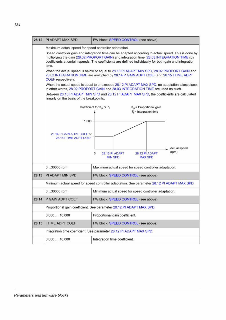
134
28.12 PI ADAPT MAX SPD FW block: SPEED CONTROL (see above)
Maximum actual speed for speed controller adaptation.Speed controller gain and integration time can be adapted according to actual speed. This is done by multiplying the gain (28.02 PROPORT GAIN) and integration time (28.03 INTEGRATION TIME) by coefficients at certain speeds. The coefficients are defined individually for both gain and integration time.When the actual speed is below or equal to 28.13 PI ADAPT MIN SPD, 28.02 PROPORT GAIN and 28.03 INTEGRATION TIME are multiplied by 28.14 P GAIN ADPT COEF and 28.15 I TIME ADPT COEF respectively.When the actual speed is equal to or exceeds 28.12 PI ADAPT MAX SPD, no adaptation takes place; in other words, 28.02 PROPORT GAIN and 28.03 INTEGRATION TIME are used as such.Between 28.13 PI ADAPT MIN SPD and 28.12 PI ADAPT MAX SPD, the coefficients are calculated linearly on the basis of the breakpoints.
0…30000 rpm Maximum actual speed for speed controller adaptation.
28.13 PI ADAPT MIN SPD FW block: SPEED CONTROL (see above)
Minimum actual speed for speed controller adaptation. See parameter 28.12 PI ADAPT MAX SPD.
0…30000 rpm Minimum actual speed for speed controller adaptation.
28.14 P GAIN ADPT COEF FW block: SPEED CONTROL (see above)
Proportional gain coefficient. See parameter 28.12 PI ADAPT MAX SPD.
0.000 … 10.000 Proportional gain coefficient.
28.15 I TIME ADPT COEF FW block: SPEED CONTROL (see above)
Integration time coefficient. See parameter 28.12 PI ADAPT MAX SPD.
0.000 … 10.000 Integration time coefficient.
Coefficient for Kp or TI Kp = Proportional gainTI = Integration time
Actual speed (rpm)
28.14 P GAIN ADPT COEF or28.15 I TIME ADPT COEF
28.13 PI ADAPT MIN SPD
28.12 PI ADAPT MAX SPD
1.000
0
Parameters and firmware blocks
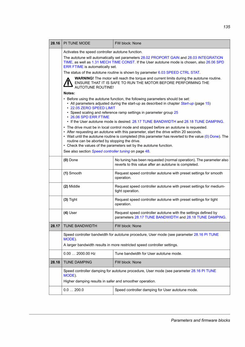
135
28.16 PI TUNE MODE FW block: None
Activates the speed controller autotune function.The autotune will automatically set parameters 28.02 PROPORT GAIN and 28.03 INTEGRATION TIME, as well as 1.31 MECH TIME CONST. If the User autotune mode is chosen, also 26.06 SPD ERR FTIME is automatically set.The status of the autotune routine is shown by parameter 6.03 SPEED CTRL STAT.
WARNING! The motor will reach the torque and current limits during the autotune routine. ENSURE THAT IT IS SAFE TO RUN THE MOTOR BEFORE PERFORMING THE AUTOTUNE ROUTINE!
Notes:• Before using the autotune function, the following parameters should be set:
• All parameters adjusted during the start-up as described in chapter Start-up (page 15)• 22.05 ZERO SPEED LIMIT• Speed scaling and reference ramp settings in parameter group 25• 26.06 SPD ERR FTIME• If the User autotune mode is desired: 28.17 TUNE BANDWIDTH and 28.18 TUNE DAMPING.
• The drive must be in local control mode and stopped before an autotune is requested.• After requesting an autotune with this parameter, start the drive within 20 seconds.• Wait until the autotune routine is completed (this parameter has reverted to the value (0) Done). The
routine can be aborted by stopping the drive.• Check the values of the parameters set by the autotune function.See also section Speed controller tuning on page 48.
(0) Done No tuning has been requested (normal operation). The parameter also reverts to this value after an autotune is completed.
(1) Smooth Request speed controller autotune with preset settings for smooth operation.
(2) Middle Request speed controller autotune with preset settings for medium-tight operation.
(3) Tight Request speed controller autotune with preset settings for tight operation.
(4) User Request speed controller autotune with the settings defined by parameters 28.17 TUNE BANDWIDTH and 28.18 TUNE DAMPING.
28.17 TUNE BANDWIDTH FW block: None
Speed controller bandwidth for autotune procedure, User mode (see parameter 28.16 PI TUNE MODE).A larger bandwidth results in more restricted speed controller settings.
0.00 … 2000.00 Hz Tune bandwidth for User autotune mode.
28.18 TUNE DAMPING FW block: None
Speed controller damping for autotune procedure, User mode (see parameter 28.16 PI TUNE MODE).Higher damping results in safer and smoother operation.
0.0 … 200.0 Speed controller damping for User autotune mode.
Parameters and firmware blocks

136
Group 32 TORQUE REFERENCEReference settings for torque control.
In torque control, the drive speed is limited between the defined minimum and maximum limits. Speed-related torque limits are calculated and the input torque reference is limited according to these limits. An OVERSPEED fault is generated if the maximum allowed speed is exceeded.
3.12 TORQUE REF ADD
3.09 TORQ REF1ZEROAI1AI2FBA REF1FBA REF2D2D REF1D2D REF2
32.01 TORQ REF1 SEL
ZEROAI1AI2FBA REF1FBA REF2D2D REF1D2D REF2
32.02 TORQ REF ADD SEL
LOCAL CONTROLLOCAL CONTROL REF
32.06 LOAD SHARE
32.04 MAXIMUM TORQ REF
32.05 MINIMUM TORQ REF
32.07 TORQ RAMP UP
32.08 TORQ RAMP DOWN
22.08 SPEED TRIP MARGIN
RUSHCTRL
1.01 SPEED ACT
20.01 MAXIMUM SPEED
20.02 MINIMUM SPEED
06.05 LIMIT WORD 1bit 5 TLIM MAX SPEEDbit 6 TLIM MIN SPEED
06.05 LIMIT WORD 1bit 3 TORQ REF MAXbit 4 TORQ REF MIN
x3.09 TORQ REF13.11 TORQ REF RUSHLIM
Parameters and firmware blocks
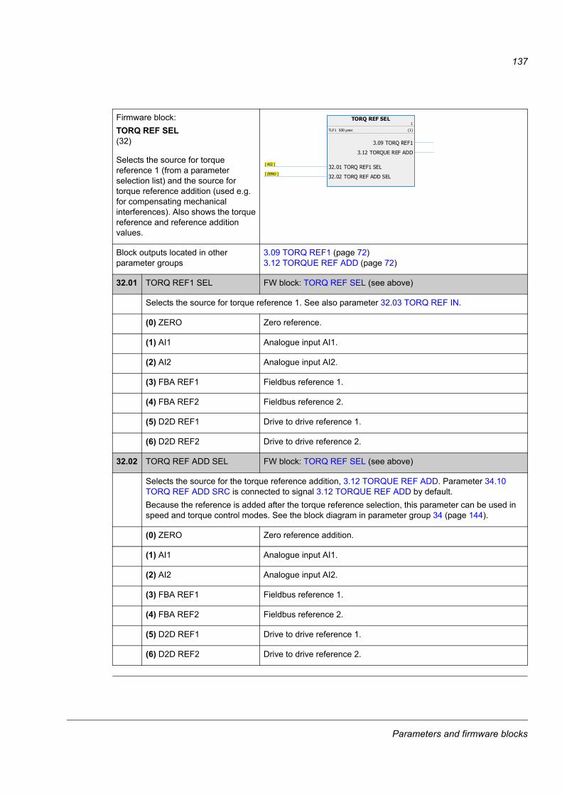
137
32Firmware block:TORQ REF SEL(32)
Selects the source for torque reference 1 (from a parameter selection list) and the source for torque reference addition (used e.g. for compensating mechanical interferences). Also shows the torque reference and reference addition values.
Block outputs located in other parameter groups
3.09 TORQ REF1 (page 72)3.12 TORQUE REF ADD (page 72)
32.01 TORQ REF1 SEL FW block: TORQ REF SEL (see above)
Selects the source for torque reference 1. See also parameter 32.03 TORQ REF IN.
(0) ZERO Zero reference.
(1) AI1 Analogue input AI1.
(2) AI2 Analogue input AI2.
(3) FBA REF1 Fieldbus reference 1.
(4) FBA REF2 Fieldbus reference 2.
(5) D2D REF1 Drive to drive reference 1.
(6) D2D REF2 Drive to drive reference 2.
32.02 TORQ REF ADD SEL FW block: TORQ REF SEL (see above)
Selects the source for the torque reference addition, 3.12 TORQUE REF ADD. Parameter 34.10 TORQ REF ADD SRC is connected to signal 3.12 TORQUE REF ADD by default.Because the reference is added after the torque reference selection, this parameter can be used in speed and torque control modes. See the block diagram in parameter group 34 (page 144).
(0) ZERO Zero reference addition.
(1) AI1 Analogue input AI1.
(2) AI2 Analogue input AI2.
(3) FBA REF1 Fieldbus reference 1.
(4) FBA REF2 Fieldbus reference 2.
(5) D2D REF1 Drive to drive reference 1.
(6) D2D REF2 Drive to drive reference 2.
TORQ REF SEL1
TLF1 500 μsec (1)
32.01 TORQ REF1 SEL [ AI2 ]
32.02 TORQ REF ADD SEL [ ZERO ]
3.09 TORQ REF1
3.12 TORQUE REF ADD
Parameters and firmware blocks
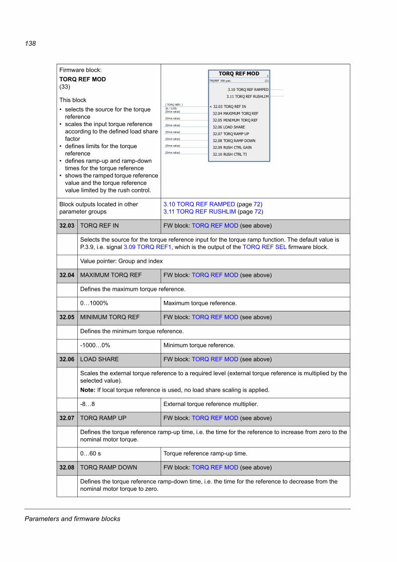
138
Firmware block:TORQ REF MOD(33)
This block• selects the source for the torque
reference• scales the input torque reference
according to the defined load share factor
• defines limits for the torque reference
• defines ramp-up and ramp-down times for the torque reference
• shows the ramped torque reference value and the torque reference value limited by the rush control.
Block outputs located in other parameter groups
3.10 TORQ REF RAMPED (page 72)3.11 TORQ REF RUSHLIM (page 72)
32.03 TORQ REF IN FW block: TORQ REF MOD (see above)
Selects the source for the torque reference input for the torque ramp function. The default value is P.3.9, i.e. signal 3.09 TORQ REF1, which is the output of the TORQ REF SEL firmware block.
Value pointer: Group and index
32.04 MAXIMUM TORQ REF FW block: TORQ REF MOD (see above)
Defines the maximum torque reference.
0…1000% Maximum torque reference.
32.05 MINIMUM TORQ REF FW block: TORQ REF MOD (see above)
Defines the minimum torque reference.
-1000…0% Minimum torque reference.
32.06 LOAD SHARE FW block: TORQ REF MOD (see above)
Scales the external torque reference to a required level (external torque reference is multiplied by the selected value).Note: If local torque reference is used, no load share scaling is applied.
-8…8 External torque reference multiplier.
32.07 TORQ RAMP UP FW block: TORQ REF MOD (see above)
Defines the torque reference ramp-up time, i.e. the time for the reference to increase from zero to the nominal motor torque.
0…60 s Torque reference ramp-up time.
32.08 TORQ RAMP DOWN FW block: TORQ REF MOD (see above)
Defines the torque reference ramp-down time, i.e. the time for the reference to decrease from the nominal motor torque to zero.
TORQ REF MOD 2
TRQREF 500 μsec (2)
< 32.03 TORQ REF IN[ TORQ REF1 ](8 / 3.09)
32.04 MAXIMUM TORQ REF(Drive value)
32.05 MINIMUM TORQ REF(Drive value)
32.06 LOAD SHARE(Drive value)
32.07 TORQ RAMP UP(Drive value)
32.08 TORQ RAMP DOWN(Drive value)
32.09 RUSH CTRL GAIN(Drive value)
32.10 RUSH CTRL TI(Drive value)
3.10 TORQ REF RAMPED
3.11 TORQ REF RUSHLIM
Parameters and firmware blocks
139
0…60 s Torque reference ramp-down time.
32.09 RUSH CTRL GAIN FW block: TORQ REF MOD (see above)
Defines the proportional gain of the rush controller.
1…10000 Proportional gain of the rush controller.
32.10 RUSH CTRL TI FW block: TORQ REF MOD (see above)
Defines the intergration time of the rush controller.
0.1…10 s Integration time of the rush controller.
Parameters and firmware blocks
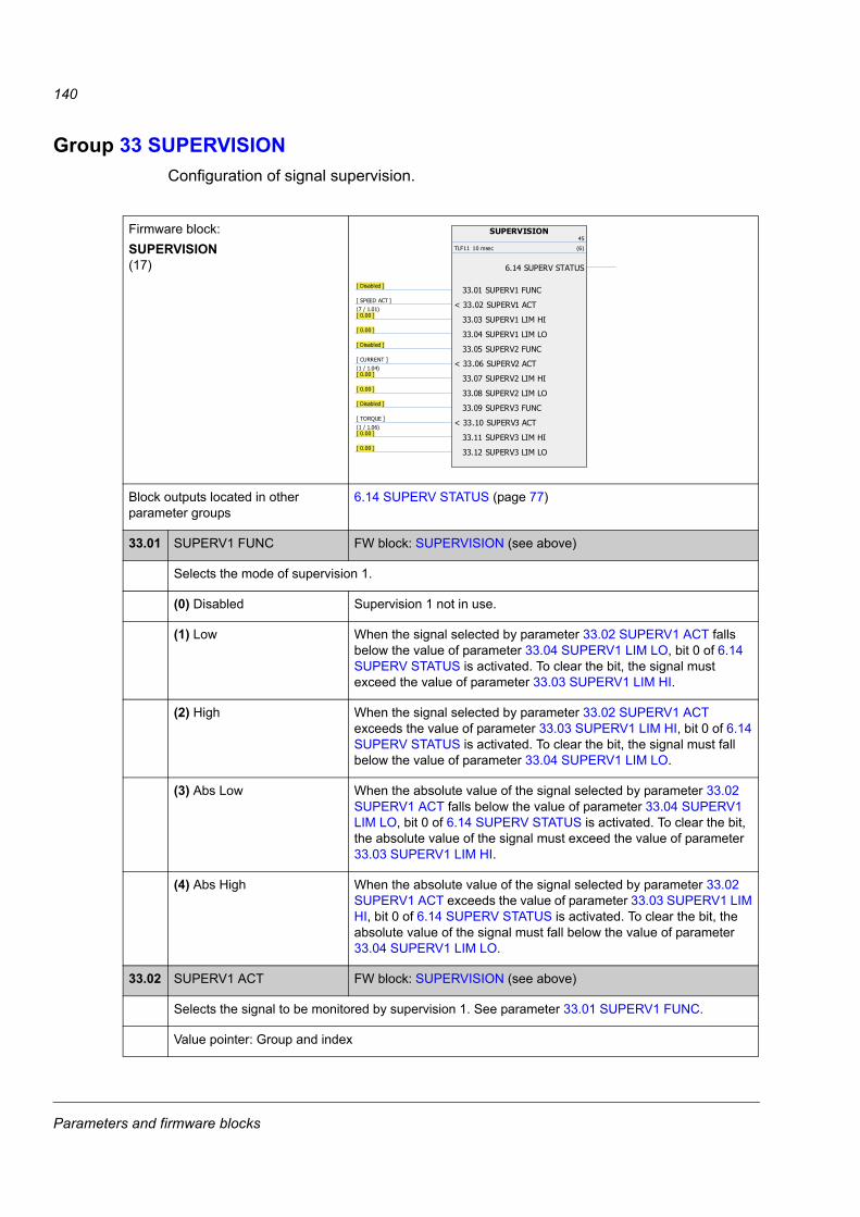
140
Group 33 SUPERVISIONConfiguration of signal supervision.
33Firmware block:SUPERVISION(17)
Block outputs located in other parameter groups
6.14 SUPERV STATUS (page 77)
33.01 SUPERV1 FUNC FW block: SUPERVISION (see above)
Selects the mode of supervision 1.
(0) Disabled Supervision 1 not in use.
(1) Low When the signal selected by parameter 33.02 SUPERV1 ACT falls below the value of parameter 33.04 SUPERV1 LIM LO, bit 0 of 6.14 SUPERV STATUS is activated. To clear the bit, the signal must exceed the value of parameter 33.03 SUPERV1 LIM HI.
(2) High When the signal selected by parameter 33.02 SUPERV1 ACT exceeds the value of parameter 33.03 SUPERV1 LIM HI, bit 0 of 6.14 SUPERV STATUS is activated. To clear the bit, the signal must fall below the value of parameter 33.04 SUPERV1 LIM LO.
(3) Abs Low When the absolute value of the signal selected by parameter 33.02 SUPERV1 ACT falls below the value of parameter 33.04 SUPERV1 LIM LO, bit 0 of 6.14 SUPERV STATUS is activated. To clear the bit, the absolute value of the signal must exceed the value of parameter 33.03 SUPERV1 LIM HI.
(4) Abs High When the absolute value of the signal selected by parameter 33.02 SUPERV1 ACT exceeds the value of parameter 33.03 SUPERV1 LIM HI, bit 0 of 6.14 SUPERV STATUS is activated. To clear the bit, the absolute value of the signal must fall below the value of parameter 33.04 SUPERV1 LIM LO.
33.02 SUPERV1 ACT FW block: SUPERVISION (see above)
Selects the signal to be monitored by supervision 1. See parameter 33.01 SUPERV1 FUNC.
Value pointer: Group and index
SUPERVISION45
TLF11 10 msec (6)
33.01 SUPERV1 FUNC [ Disabled ]
< 33.02 SUPERV1 ACT[ SPEED ACT ](7 / 1.01)
33.03 SUPERV1 LIM HI [ 0.00 ]
33.04 SUPERV1 LIM LO [ 0.00 ]
33.05 SUPERV2 FUNC [ Disabled ]
< 33.06 SUPERV2 ACT[ CURRENT ](1 / 1.04)
33.07 SUPERV2 LIM HI [ 0.00 ]
33.08 SUPERV2 LIM LO [ 0.00 ]
33.09 SUPERV3 FUNC [ Disabled ]
< 33.10 SUPERV3 ACT[ TORQUE ](1 / 1.06)
33.11 SUPERV3 LIM HI [ 0.00 ]
33.12 SUPERV3 LIM LO [ 0.00 ]
6.14 SUPERV STATUS
Parameters and firmware blocks
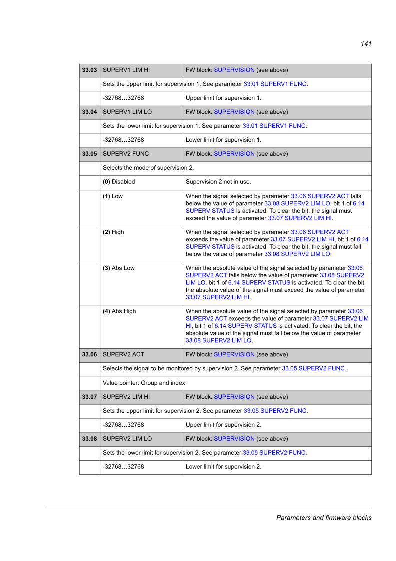
141
33.03 SUPERV1 LIM HI FW block: SUPERVISION (see above)
Sets the upper limit for supervision 1. See parameter 33.01 SUPERV1 FUNC.
-32768…32768 Upper limit for supervision 1.
33.04 SUPERV1 LIM LO FW block: SUPERVISION (see above)
Sets the lower limit for supervision 1. See parameter 33.01 SUPERV1 FUNC.
-32768…32768 Lower limit for supervision 1.
33.05 SUPERV2 FUNC FW block: SUPERVISION (see above)
Selects the mode of supervision 2.
(0) Disabled Supervision 2 not in use.
(1) Low When the signal selected by parameter 33.06 SUPERV2 ACT falls below the value of parameter 33.08 SUPERV2 LIM LO, bit 1 of 6.14 SUPERV STATUS is activated. To clear the bit, the signal must exceed the value of parameter 33.07 SUPERV2 LIM HI.
(2) High When the signal selected by parameter 33.06 SUPERV2 ACT exceeds the value of parameter 33.07 SUPERV2 LIM HI, bit 1 of 6.14 SUPERV STATUS is activated. To clear the bit, the signal must fall below the value of parameter 33.08 SUPERV2 LIM LO.
(3) Abs Low When the absolute value of the signal selected by parameter 33.06 SUPERV2 ACT falls below the value of parameter 33.08 SUPERV2 LIM LO, bit 1 of 6.14 SUPERV STATUS is activated. To clear the bit, the absolute value of the signal must exceed the value of parameter 33.07 SUPERV2 LIM HI.
(4) Abs High When the absolute value of the signal selected by parameter 33.06 SUPERV2 ACT exceeds the value of parameter 33.07 SUPERV2 LIM HI, bit 1 of 6.14 SUPERV STATUS is activated. To clear the bit, the absolute value of the signal must fall below the value of parameter 33.08 SUPERV2 LIM LO.
33.06 SUPERV2 ACT FW block: SUPERVISION (see above)
Selects the signal to be monitored by supervision 2. See parameter 33.05 SUPERV2 FUNC.
Value pointer: Group and index
33.07 SUPERV2 LIM HI FW block: SUPERVISION (see above)
Sets the upper limit for supervision 2. See parameter 33.05 SUPERV2 FUNC.
-32768…32768 Upper limit for supervision 2.
33.08 SUPERV2 LIM LO FW block: SUPERVISION (see above)
Sets the lower limit for supervision 2. See parameter 33.05 SUPERV2 FUNC.
-32768…32768 Lower limit for supervision 2.
Parameters and firmware blocks
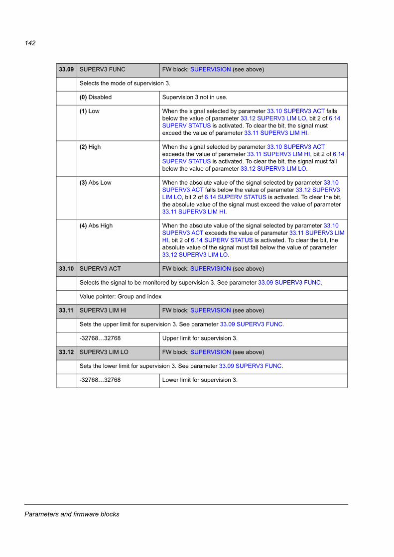
142
33.09 SUPERV3 FUNC FW block: SUPERVISION (see above)
Selects the mode of supervision 3.
(0) Disabled Supervision 3 not in use.
(1) Low When the signal selected by parameter 33.10 SUPERV3 ACT falls below the value of parameter 33.12 SUPERV3 LIM LO, bit 2 of 6.14 SUPERV STATUS is activated. To clear the bit, the signal must exceed the value of parameter 33.11 SUPERV3 LIM HI.
(2) High When the signal selected by parameter 33.10 SUPERV3 ACT exceeds the value of parameter 33.11 SUPERV3 LIM HI, bit 2 of 6.14 SUPERV STATUS is activated. To clear the bit, the signal must fall below the value of parameter 33.12 SUPERV3 LIM LO.
(3) Abs Low When the absolute value of the signal selected by parameter 33.10 SUPERV3 ACT falls below the value of parameter 33.12 SUPERV3 LIM LO, bit 2 of 6.14 SUPERV STATUS is activated. To clear the bit, the absolute value of the signal must exceed the value of parameter 33.11 SUPERV3 LIM HI.
(4) Abs High When the absolute value of the signal selected by parameter 33.10 SUPERV3 ACT exceeds the value of parameter 33.11 SUPERV3 LIM HI, bit 2 of 6.14 SUPERV STATUS is activated. To clear the bit, the absolute value of the signal must fall below the value of parameter 33.12 SUPERV3 LIM LO.
33.10 SUPERV3 ACT FW block: SUPERVISION (see above)
Selects the signal to be monitored by supervision 3. See parameter 33.09 SUPERV3 FUNC.
Value pointer: Group and index
33.11 SUPERV3 LIM HI FW block: SUPERVISION (see above)
Sets the upper limit for supervision 3. See parameter 33.09 SUPERV3 FUNC.
-32768…32768 Upper limit for supervision 3.
33.12 SUPERV3 LIM LO FW block: SUPERVISION (see above)
Sets the lower limit for supervision 3. See parameter 33.09 SUPERV3 FUNC.
-32768…32768 Lower limit for supervision 3.
Parameters and firmware blocks
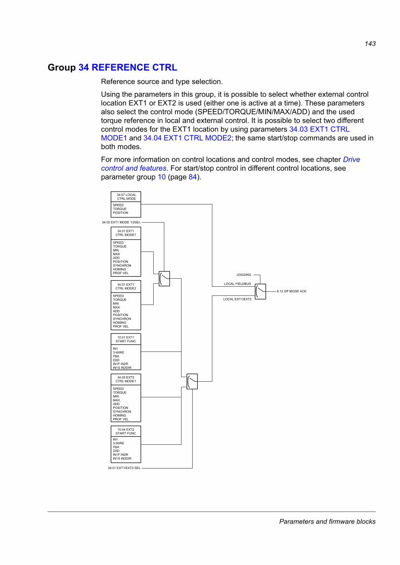
143
Group 34 REFERENCE CTRLReference source and type selection.
Using the parameters in this group, it is possible to select whether external control location EXT1 or EXT2 is used (either one is active at a time). These parameters also select the control mode (SPEED/TORQUE/MIN/MAX/ADD) and the used torque reference in local and external control. It is possible to select two different control modes for the EXT1 location by using parameters 34.03 EXT1 CTRL MODE1 and 34.04 EXT1 CTRL MODE2; the same start/stop commands are used in both modes.
For more information on control locations and control modes, see chapter Drive control and features. For start/stop control in different control locations, see parameter group 10 (page 84).
IN13-WIREFBAD2DIN1F IN2RIN1S IN2DIR
10.01 EXT1 START FUNC
34.02 EXT1 MODE 1/2SEL
SPEEDTORQUEPOSITION
34.07 LOCAL CTRL MODE
34.01 EXT1/EXT2 SEL
IN13-WIREFBAD2DIN1F IN2RIN1S IN2DIR
10.04 EXT2 START FUNC
SPEEDTORQUEMINMAXADDPOSITIONSYNCHRONHOMINGPROF VEL
34.05 EXT2 CTRL MODE1
6.12 OP MODE ACK
SPEEDTORQUEMINMAXADDPOSITIONSYNCHRONHOMINGPROF VEL
34.01 EXT1 CTRL MODE1
SPEEDTORQUEMINMAXADDPOSITIONSYNCHRONHOMINGPROF VEL
34.01 EXT1 CTRL MODE2
JOGGING
LOCAL EXT1/EXT2
LOCAL FIELDBUS
Parameters and firmware blocks
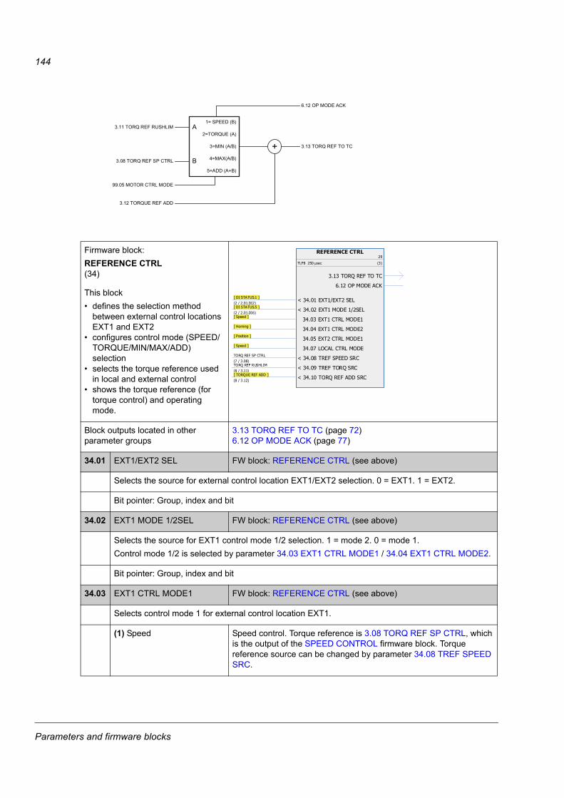
144
34Firmware block:REFERENCE CTRL(34)
This block• defines the selection method
between external control locations EXT1 and EXT2
• configures control mode (SPEED/TORQUE/MIN/MAX/ADD) selection
• selects the torque reference used in local and external control
• shows the torque reference (for torque control) and operating mode.
Block outputs located in other parameter groups
3.13 TORQ REF TO TC (page 72)6.12 OP MODE ACK (page 77)
34.01 EXT1/EXT2 SEL FW block: REFERENCE CTRL (see above)
Selects the source for external control location EXT1/EXT2 selection. 0 = EXT1. 1 = EXT2.
Bit pointer: Group, index and bit
34.02 EXT1 MODE 1/2SEL FW block: REFERENCE CTRL (see above)
Selects the source for EXT1 control mode 1/2 selection. 1 = mode 2. 0 = mode 1.Control mode 1/2 is selected by parameter 34.03 EXT1 CTRL MODE1 / 34.04 EXT1 CTRL MODE2.
Bit pointer: Group, index and bit
34.03 EXT1 CTRL MODE1 FW block: REFERENCE CTRL (see above)
Selects control mode 1 for external control location EXT1.
(1) Speed Speed control. Torque reference is 3.08 TORQ REF SP CTRL, which is the output of the SPEED CONTROL firmware block. Torque reference source can be changed by parameter 34.08 TREF SPEED SRC.
1= SPEED (B)
2=TORQUE (A)
3=MIN (A/B)
4=MAX(A/B)
5=ADD (A+B)
3.08 TORQ REF SP CTRL
99.05 MOTOR CTRL MODE
+ 3.13 TORQ REF TO TC
3.11 TORQ REF RUSHLIM
6.12 OP MODE ACK
3.12 TORQUE REF ADD
A
B
REFERENCE CTRL29
TLF8 250 μsec (3)
< 34.01 EXT1/EXT2 SEL [ DI STATUS.1 ](2 / 2.01.DI2)
< 34.02 EXT1 MODE 1/2SEL [ DI STATUS.5 ](2 / 2.01.DI6)
34.03 EXT1 CTRL MODE1 [ Speed ]
34.04 EXT1 CTRL MODE2 [ Homing ]
34.05 EXT2 CTRL MODE1 [ Position ]
34.07 LOCAL CTRL MODE [ Speed ]
< 34.08 TREF SPEED SRCTORQ REF SP CTRL(7 / 3.08)
< 34.09 TREF TORQ SRCTORQ REF RUSHLIM(8 / 3.11)
< 34.10 TORQ REF ADD SRC [ TORQUE REF ADD ](8 / 3.12)
3.13 TORQ REF TO TC
6.12 OP MODE ACK
Parameters and firmware blocks
145
(2) Torque Torque control. Torque reference is 3.11 TORQ REF RUSHLIM, which is the output of the TORQ REF MOD firmware block. Torque reference source can be changed by parameter 34.09 TREF TORQ SRC.
(3) Min Combination of selections (1) Speed and (2) Torque: Torque selector compares the torque reference and the speed controller output and the smaller of them is used.
(4) Max Combination of selections (1) Speed and (2) Torque: Torque selector compares the torque reference and the speed controller output and the greater of them is used.
(5) Add Combination of selections (1) Speed and (2) Torque: Torque selector adds the speed controller output to the torque reference.
34.04 EXT1 CTRL MODE2 FW block: REFERENCE CTRL (see above)
Selects control mode 2 for external control location EXT1.For selections, see parameter 34.03 EXT1 CTRL MODE1.
34.05 EXT2 CTRL MODE1 FW block: REFERENCE CTRL (see above)
Selects control mode for external control location EXT2. For selections, see parameter 34.03 EXT1 CTRL MODE1.
34.07 LOCAL CTRL MODE FW block: REFERENCE CTRL (see above)
Selects the control mode for local control.Note: This parameter cannot be changed while the drive is running.
(1) Speed Speed control. Torque reference is 3.08 TORQ REF SP CTRL, which is the output of the SPEED CONTROL firmware block. Torque reference source can be changed by parameter 34.08 TREF SPEED SRC.
(2) Torque Torque control. Torque reference is 3.11 TORQ REF RUSHLIM, which is an output of the TORQ REF MOD firmware block. Torque reference source can be changed by parameter 34.09 TREF TORQ SRC.
34.08 TREF SPEED SRC FW block: REFERENCE CTRL (see above)
Selects the source for the torque reference (from the speed controller). Default value is P.3.8, i.e. 3.08 TORQ REF SP CTRL, which is the output of the SPEED CONTROL firmware block.Note: This parameter has been locked, i.e. no user setting is possible.
Value pointer: Group and index
34.09 TREF TORQ SRC FW block: REFERENCE CTRL (see above)
Selects the source for the torque reference (from the torque reference chain). Default value is P.3.11, i.e. 3.11 TORQ REF RUSHLIM, which is an output of the TORQ REF MOD firmware block.Note: This parameter has been locked, i.e. no user setting is possible.
Value pointer: Group and index
Parameters and firmware blocks

146
34.10 TORQ REF ADD SRC FW block: REFERENCE CTRL (see above)
Selects the source for the torque reference added to the torque value after the torque selection. Default value is P.3.12, i.e. 3.12 TORQUE REF ADD, which is an output of the TORQ REF SEL firmware block.Note: This parameter has been locked, i.e. no user setting is possible.
Value pointer: Group and index
Parameters and firmware blocks
147
Group 35 MECH BRAKE CTRLSettings for the control of a mechanical brake. See also section Mechanical brake control on page 52.
35Firmware block:MECH BRAKE CTRL(35)
Block outputs located in other parameter groups
3.14 BRAKE TORQ MEM (page 72)3.15 BRAKE COMMAND (page 73)
35.01 BRAKE CONTROL FW block: MECH BRAKE CTRL (see above)
Activates the brake control function with or without supervision.Note: This parameter cannot be changed while the drive is running.
(0) NO Inactive.
(1) WITH ACK Brake control with supervision (supervision is activated by parameter 35.02 BRAKE ACKNOWL).
(2) NO ACK Brake control without supervision.
35.02 BRAKE ACKNOWL FW block: MECH BRAKE CTRL (see above)
Selects the source for the external brake on/off supervision activation (when par. 35.01 BRAKE CONTROL = (1) WITH ACK). The use of the external on/off supervision signal is optional. 1 = The brake is open. 0 = The brake is closed.Brake supervision is usually controlled with a digital input. It can also be controlled with an external control system, e.g. fieldbus.When brake control error is detected the drive reacts as defined by parameter 35.09 BRAKE FAULT FUNC.Note: This parameter cannot be changed while the drive is running.
Bit pointer: Group, index and bit
MECH BRAKE CTRL30
TLF10 2 msec (2)
35.01 BRAKE CONTROL [ NO ]
< 35.02 BRAKE ACKNOWL [ FALSE ]
35.03 BRAKE OPEN DELAY [ 0.00 s ]
35.04 BRAKE CLOSE DLY [ 0.00 s ]
35.05 BRAKE CLOSE SPD [ 100.0 rpm ]
35.06 BRAKE OPEN TORQ [ 0.0 % ]
< 35.07 BRAKE CLOSE REQ [ FALSE ]
< 35.08 BRAKE OPEN HOLD [ FALSE ]
35.09 BRAKE FAULT FUNC [ FAULT ]
3.14 BRAKE TORQ MEM
3.15 BRAKE COMMAND
Parameters and firmware blocks
148
35.03 BRAKE OPEN DELAY FW block: MECH BRAKE CTRL (see above)
Defines the brake open delay (= the delay between the internal open brake command and the release of the motor speed control). The delay counter starts when the drive has magnetised the motor and risen the motor torque to the level required at the brake release (parameter 35.06 BRAKE OPEN TORQ). Simultaneously with the counter start, the brake function energises the relay output controlling the brake and the brake starts opening.Set the delay the same as the mechanical opening delay of the brake specified by the brake manufacturer.
0…5 s Brake open delay.
35.04 BRAKE CLOSE DLY FW block: MECH BRAKE CTRL (see above)
Defines the brake close delay. The delay counter starts when the motor actual speed has fallen below the set level (parameter 35.05 BRAKE CLOSE SPD) after the drive has received the stop command. Simultaneously with the counter start, the brake control function de-energises the relay output controlling the brake and the brake starts closing. During the delay, the brake function keeps the motor live preventing the motor speed from falling below zero.Set the delay time to the same value as the mechanical make-up time of the brake (= operating delay when closing) specified by the brake manufacturer.
0…60 s Brake close delay.
35.05 BRAKE CLOSE SPD FW block: MECH BRAKE CTRL (see above)
Defines the brake close speed (an absolute value). See parameter 35.04 BRAKE CLOSE DLY.
0…1000 rpm Brake close speed.
35.06 BRAKE OPEN TORQ FW block: MECH BRAKE CTRL (see above)
Defines the motor starting torque at brake release (in percent of the motor nominal torque).
0…1000% Motor starting torque at brake release.
35.07 BRAKE CLOSE REQ FW block: MECH BRAKE CTRL (see above)
Selects the source for the brake close (open) request. 1 = Brake close request. 0 = Brake open request.Note: This parameter cannot be changed while the drive is running.
Bit pointer: Group, index and bit
35.08 BRAKE OPEN HOLD FW block: MECH BRAKE CTRL (see above)
Selects the source for the activation of the brake open command hold. 1 = Hold active. 0 = Normal operation.Note: This parameter cannot be changed while the drive is running.
Bit pointer: Group, index and bit
35.09 BRAKE FAULT FUNC FW block: MECH BRAKE CTRL (see above)
Defines how the drive reacts in case of mechanical brake control error. If brake control supervision has not been activated by parameter 35.01 BRAKE CONTROL, this parameter is disabled.
Parameters and firmware blocks
149
(0) FAULT The drive trips on fault BRAKE NOT CLOSED / BRAKE NOT OPEN if the status of the optional external brake acknowledgement signal does not meet the status presumed by the brake control function. The drive trips on fault BRAKE START TORQUE if the required motor starting torque at brake release is not achieved.
(1) ALARM The drive generates alarm BRAKE NOT CLOSED / BRAKE NOT OPEN if the status of the optional external brake acknowledgement signal does not meet the status presumed by the brake control function. The drive generates alarm BRAKE START TORQUE if the required motor starting torque at brake release is not achieved.
(2) OPEN FLT The drive generates alarm BRAKE NOT CLOSED (when closing the brake) and trips on fault BRAKE NOT OPEN (when opening the brake) if the status of the optional external brake acknowledgement signal does not match the status presumed by the brake control function. The drive trips on BRAKE START TORQUE if the required motor start torque at brake release is not achieved.
Parameters and firmware blocks

150
Group 40 MOTOR CONTROLMotor control settings, such as
• flux reference
• drive switching frequency
• motor slip compensation
• voltage reserve
• flux optimisation
• IR compensation for scalar control mode.
Flux optimisation
Flux optimisation reduces the total energy consumption and motor noise level when the drive operates below the nominal load. The total efficiency (motor and drive) can be improved by 1% to 10%, depending on the load torque and speed.
Note: Flux optimisation limits the dynamic control performance of the drive because with a small flux reference the drive torque cannot be increased fast.
40Firmware block:MOTOR CONTROL(40)
This block defines motor control settings such as• flux reference• drive switching frequency• motor slip compensation• voltage reserve• flux optimisation• IR compensation for scalar control
mode• flux braking.The block also shows the flux and torque reference used.
Block outputs located in other parameter groups
3.16 FLUX REF USED (page 73)3.17 TORQUE REF USED (page 73)
40.01 FLUX REF FW block: MOTOR CONTROL (see above)
Defines the flux reference.
0…200% Flux reference.
40.02 SF REF FW block: MOTOR CONTROL (see above)
Defines the switching frequency of the drive.When switching frequency exceeds 4 kHz, the allowed drive output current is limited. See switching frequency derating in the appropriate Hardware Manual.
1/2/3/4/5/8/16 kHz Switching frequency.
MOTOR CONTROL 31
MISC_3 2 msec (9)
40.01 FLUX REF(Drive value)
40.02 SF REF(Drive value)
40.03 SLIP GAIN(Drive value)
40.04 VOLTAGE RESERVE(Drive value)
40.05 FLUX OPT(Drive value)
40.06 FORCE OPEN LOOP(Drive value)
40.07 IR COMPENSATION(Drive value)
40.10 FLUX BRAKING(Drive value)
3.16 FLUX REF USED
3.17 TORQUE REF USED
Parameters and firmware blocks
151
40.03 SLIP GAIN FW block: MOTOR CONTROL (see above)
Defines the slip gain which is used to improve the estimated motor slip. 100% means full slip gain; 0% means no slip gain. The default value is 100%. Other values can be used if a static speed error is detected despite of the full slip gain.Example (with nominal load and nominal slip of 40 rpm): A 1000 rpm constant speed reference is given to the drive. Despite of the full slip gain (= 100%), a manual tachometer measurement from the motor axis gives a speed value of 998 rpm. The static speed error is 1000 rpm - 998 rpm = 2 rpm. To compensate the error, the slip gain should be increased. At the 105% gain value, no static speed error exists (2 rpm / 40 rpm = 5%).
0…200% Slip gain.
40.04 VOLTAGE RESERVE FW block: MOTOR CONTROL (see above)
Defines the minimum allowed voltage reserve. When the voltage reserve has decreased to the set value, the drive enters the field weakening area.If the intermediate circuit DC voltage Udc = 550 V and the voltage reserve is 5%, the RMS value of the maximum output voltage in steady-state operation is 0.95 × 550 V / sqrt(2) = 369 VThe dynamic performance of the motor control in the field weakening area can be improved by increasing the voltage reserve value, but the drive enters the field weakening area earlier.
-4…50% Minimum allowed voltage reserve.
40.05 FLUX OPT FW block: MOTOR CONTROL (see above)
Enables the flux optimisation function. Flux optimisation improves motor efficiency and reduces noise. Flux optimisation is used in drives that usually operate below nominal load.Note: With a permanent magnet motor, flux optimisation is always enabled regardless of this parameter.
(0) Disable Flux optimisation disabled.
(1) Enable Flux optimisation enabled.
40.06 FORCE OPEN LOOP FW block: MOTOR CONTROL (see above)
Defines the speed/position information used by the motor model.
(0) FALSE Motor model uses the speed feedback selected by parameter 22.01 SPEED FB SEL.
(1) TRUE Motor model uses the internal speed estimate (even when parameter 22.01 SPEED FB SEL setting is (1) Enc1 speed / (2) Enc2 speed).
Parameters and firmware blocks
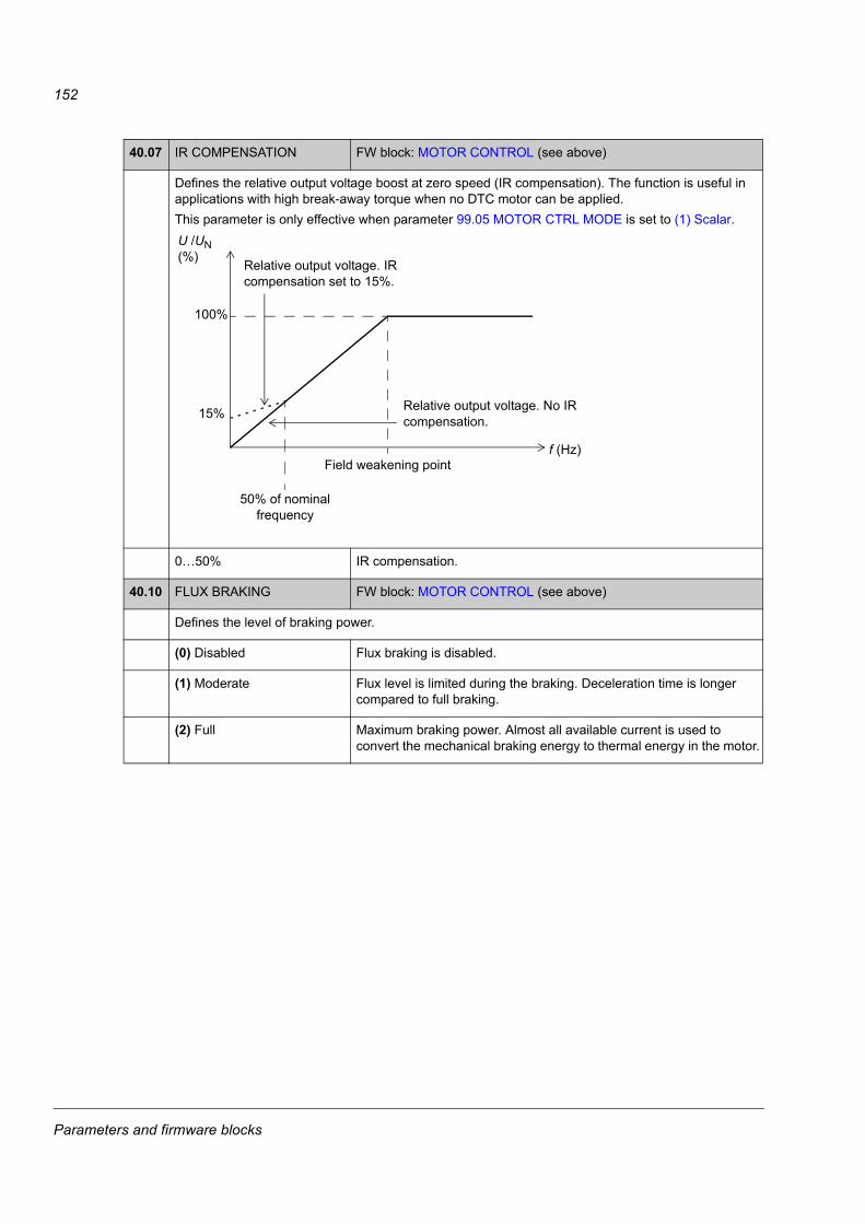
152
40.07 IR COMPENSATION FW block: MOTOR CONTROL (see above)
Defines the relative output voltage boost at zero speed (IR compensation). The function is useful in applications with high break-away torque when no DTC motor can be applied.This parameter is only effective when parameter 99.05 MOTOR CTRL MODE is set to (1) Scalar.
0…50% IR compensation.
40.10 FLUX BRAKING FW block: MOTOR CONTROL (see above)
Defines the level of braking power.
(0) Disabled Flux braking is disabled.
(1) Moderate Flux level is limited during the braking. Deceleration time is longer compared to full braking.
(2) Full Maximum braking power. Almost all available current is used to convert the mechanical braking energy to thermal energy in the motor.
U /UN(%)
f (Hz)Field weakening point
Relative output voltage. No IR compensation.
Relative output voltage. IR compensation set to 15%.
15%
100%
50% of nominal frequency
Parameters and firmware blocks
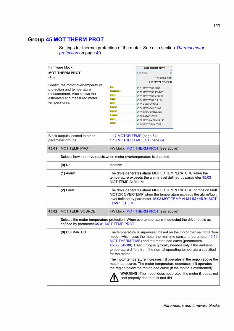
153
Group 45 MOT THERM PROTSettings for thermal protection of the motor. See also section Thermal motor protection on page 40.
45Firmware block:MOT THERM PROT(45)
Configures motor overtemperature protection and temperature measurement. Also shows the estimated and measured motor temperatures.
Block outputs located in other parameter groups
1.17 MOTOR TEMP (page 64)1.18 MOTOR TEMP EST (page 64)
45.01 MOT TEMP PROT FW block: MOT THERM PROT (see above)
Selects how the drive reacts when motor overtemperature is detected.
(0) No Inactive.
(1) Alarm The drive generates alarm MOTOR TEMPERATURE when the temperature exceeds the alarm level defined by parameter 45.03 MOT TEMP ALM LIM.
(2) Fault The drive generates alarm MOTOR TEMPERATURE or trips on fault MOTOR OVERTEMP when the temperature exceeds the alarm/fault level defined by parameter 45.03 MOT TEMP ALM LIM / 45.04 MOT TEMP FLT LIM.
45.02 MOT TEMP SOURCE FW block: MOT THERM PROT (see above)
Selects the motor temperature protection. When overtemperature is detected the drive reacts as defined by parameter 45.01 MOT TEMP PROT.
(0) ESTIMATED The temperature is supervised based on the motor thermal protection model, which uses the motor thermal time constant (parameter 45.10 MOT THERM TIME) and the motor load curve (parameters 45.06…45.08). User tuning is typically needed only if the ambient temperature differs from the normal operating temperature specified for the motor.The motor temperature increases if it operates in the region above the motor load curve. The motor temperature decreases if it operates in the region below the motor load curve (if the motor is overheated).
WARNING! The model does not protect the motor if it does not cool properly due to dust and dirt.
MOT THERM PROT32
TLF11 10 msec (5)
45.01 MOT TEMP PROT [ No ]
45.02 MOT TEMP SOURCE [ ESTIMATED ]
45.03 MOT TEMP ALM LIM [ 90 C ]
45.04 MOT TEMP FLT LIM [ 110 C ]
45.05 AMBIENT TEMP [ 20 C ]
45.06 MOT LOAD CURVE [ 100 % ]
45.07 ZERO SPEED LOAD [ 100 % ]
45.08 BREAK POINT [ 45.00 Hz ]
45.09 MOTNOM TEMP RISE [ 80 C ]
45.10 MOT THERM TIME [ 256 s ]
1.17 MOTOR TEMP
1.18 MOTOR TEMP EST
Parameters and firmware blocks

154
(1) KTY JCU The temperature is supervised using a KTY84 sensor connected to drive thermistor input TH.
(2) KTY 1st FEN The temperature is supervised using a KTY84 sensor connected to encoder interface module FEN-xx installed in drive Slot 1/2. If two encoder interface modules are used, encoder module connected to Slot 1 is used for the temperature supervision. Note: This selection does not apply for FEN-01. *
(3) KTY 2nd FEN The temperature is supervised using a KTY84 sensor connected to encoder interface module FEN-xx installed in drive Slot 1/2. If two encoder interface modules are used, encoder module connected to Slot 2 is used for the temperature supervision. Note: This selection does not apply for FEN-01. *
(4) PTC JCU The temperature is supervised using 1…3 PTC sensors connected to drive thermistor input TH.
(5) PTC 1st FEN The temperature is supervised using 1…3 PTC sensors connected to encoder interface module FEN-xx installed in drive Slot 1/2. If two encoder interface modules are used, encoder module connected to Slot 1 is used for the temperature supervision. *
(6) PTC 2nd FEN The temperature is supervised using 1…3 PTC sensors connected to encoder interface module FEN-xx installed in drive Slot 1/2. If two encoder interface modules are used, encoder module connected to Slot 2 is used for the temperature supervision. *
*Note: If one FEN-xx module is used, parameter setting must be either (2) KTY 1st FEN or (5) PTC 1st FEN. The FEN-xx module can be in either Slot 1 or Slot 2.
45.03 MOT TEMP ALM LIM FW block: MOT THERM PROT (see above)
Defines the alarm limit for the motor overtemperature protection (when par. 45.01 MOT TEMP PROT = (1) Alarm or (2) Fault).
0…200 °C Motor overtemperature alarm limit.
45.04 MOT TEMP FLT LIM FW block: MOT THERM PROT (see above)
Defines the fault limit for the motor overtemperature protection (when par. 45.01 MOT TEMP PROT = (2) Fault).
0…200 °C Motor overtemperature fault limit.
45.05 AMBIENT TEMP FW block: MOT THERM PROT (see above)
Defines the ambient temperature for the thermal protection mode.
-60…100 °C Ambient temperature.
Parameters and firmware blocks
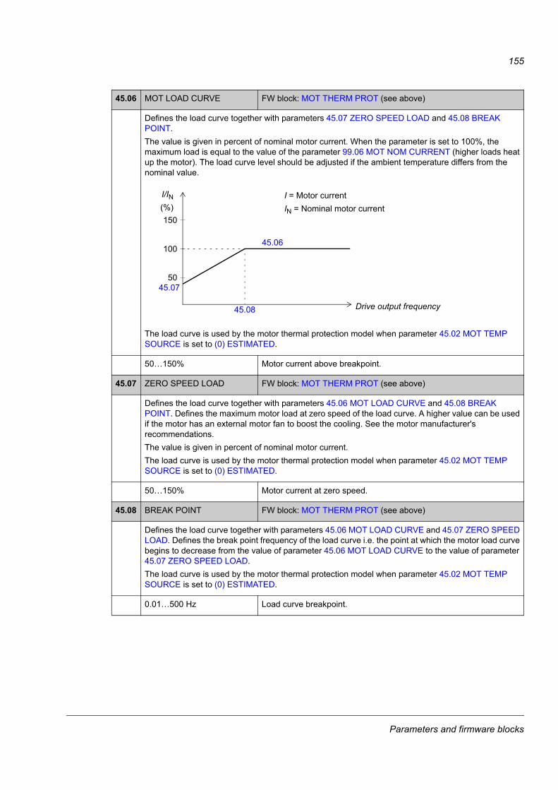
155
45.06 MOT LOAD CURVE FW block: MOT THERM PROT (see above)
Defines the load curve together with parameters 45.07 ZERO SPEED LOAD and 45.08 BREAK POINT.The value is given in percent of nominal motor current. When the parameter is set to 100%, the maximum load is equal to the value of the parameter 99.06 MOT NOM CURRENT (higher loads heat up the motor). The load curve level should be adjusted if the ambient temperature differs from the nominal value.
The load curve is used by the motor thermal protection model when parameter 45.02 MOT TEMP SOURCE is set to (0) ESTIMATED.
50…150% Motor current above breakpoint.
45.07 ZERO SPEED LOAD FW block: MOT THERM PROT (see above)
Defines the load curve together with parameters 45.06 MOT LOAD CURVE and 45.08 BREAK POINT. Defines the maximum motor load at zero speed of the load curve. A higher value can be used if the motor has an external motor fan to boost the cooling. See the motor manufacturer's recommendations. The value is given in percent of nominal motor current.The load curve is used by the motor thermal protection model when parameter 45.02 MOT TEMP SOURCE is set to (0) ESTIMATED.
50…150% Motor current at zero speed.
45.08 BREAK POINT FW block: MOT THERM PROT (see above)
Defines the load curve together with parameters 45.06 MOT LOAD CURVE and 45.07 ZERO SPEED LOAD. Defines the break point frequency of the load curve i.e. the point at which the motor load curve begins to decrease from the value of parameter 45.06 MOT LOAD CURVE to the value of parameter 45.07 ZERO SPEED LOAD. The load curve is used by the motor thermal protection model when parameter 45.02 MOT TEMP SOURCE is set to (0) ESTIMATED.
0.01…500 Hz Load curve breakpoint.
50
100
150
45.06
45.08
45.07
I/IN(%)
I = Motor currentIN = Nominal motor current
Drive output frequency
Parameters and firmware blocks
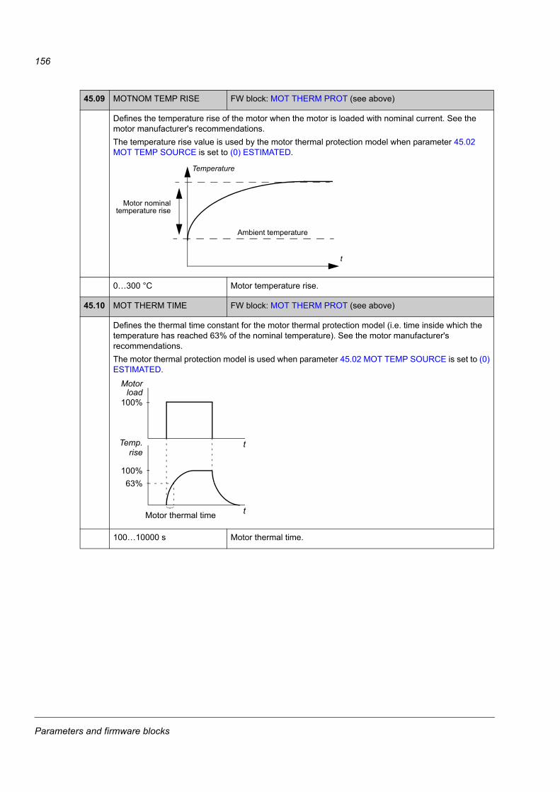
156
45.09 MOTNOM TEMP RISE FW block: MOT THERM PROT (see above)
Defines the temperature rise of the motor when the motor is loaded with nominal current. See the motor manufacturer's recommendations.The temperature rise value is used by the motor thermal protection model when parameter 45.02 MOT TEMP SOURCE is set to (0) ESTIMATED.
0…300 °C Motor temperature rise.
45.10 MOT THERM TIME FW block: MOT THERM PROT (see above)
Defines the thermal time constant for the motor thermal protection model (i.e. time inside which the temperature has reached 63% of the nominal temperature). See the motor manufacturer's recommendations.The motor thermal protection model is used when parameter 45.02 MOT TEMP SOURCE is set to (0) ESTIMATED.
100…10000 s Motor thermal time.
t
Temperature
Ambient temperature
Motor nominaltemperature rise
Motor
100%
Temp.
63%
Motor thermal time
t
t
100%load
rise
Parameters and firmware blocks

157
Group 46 FAULT FUNCTIONSDefinition of drive behaviour upon a fault situation.
An alarm or a fault message indicates abnormal drive status. For the possible causes and remedies, see chapter Fault tracing.
46Firmware block:FAULT FUNCTIONS(46)
This block• configures supervision of external
faults by defining the source (for example, a digital input) for external fault indication signal
• selects the reaction of the drive (alarm; fault; continuation at safe speed in some cases) upon situations like local control communication break, motor/supply phase loss, earth fault, or Safe Torque Off function activation
• shows the codes of the latest faults, the time at which the active fault occurred, and the alarm words.
Block inputs located in other parameter groups
22.10 SPD SUPERV EST (page 116)22.11 SPD SUPERV ENC (page 116)22.12 SPD SUPERV FILT (page 116)
Block outputs located in other parameter groups
8.01 ACTIVE FAULT (page 78)8.02 LAST FAULT (page 78)8.03 FAULT TIME HI (page 78)8.04 FAULT TIME LO (page 78)8.05 ALARM LOGGER 1 (page 78)8.06 ALARM LOGGER 2 (page 79)8.07 ALARM LOGGER 3 (page 79)8.08 ALARM LOGGER 4 (page 80)8.09 ALARM LOGGER 5 (page 80)8.10 ALARM LOGGER 6 (page 80)8.15 ALARM WORD 1 (page 81)8.16 ALARM WORD 2 (page 81)8.17 ALARM WORD 3 (page 82)8.18 ALARM WORD 4 (page 82)
FAULT FUNCTIONS 33
MISC_3 2 msec (10)
22.10 SPD SUPERV EST(Drive value)
22.11 SPD SUPERV ENC(Drive value)
22.12 SPD SUPERV FILT(Drive value)
< 46.01 EXTERNAL FAULT(Drive value)
46.02 SPEED REF SAFE(Drive value)
46.03 LOCAL CTRL LOSS(Drive value)
46.04 MOT PHASE LOSS(Drive value)
46.05 EARTH FAULT(Drive value)
46.06 SUPPL PHS LOSS(Drive value)
46.07 STO DIAGNOSTIC(Drive value)
46.08 CROSS CONNECTION(Drive value)
46.09 STALL FUNCTION(Drive value)
46.10 STALL CURR LIM(Drive value)
46.11 STALL FREQ HI(Drive value)
46.12 STALL TIME(Drive value)
8.01 ACTIVE FAULT
8.02 LAST FAULT
8.03 FAULT TIME HI
8.04 FAULT TIME LO
8.05 ALARM LOGGER 1
8.06 ALARM LOGGER 2
8.07 ALARM LOGGER 3
8.08 ALARM LOGGER 4
8.09 ALARM LOGGER 5
8.10 ALARM LOGGER 6
8.15 ALARM WORD 1
8.16 ALARM WORD 2
8.17 ALARM WORD 3
8.18 ALARM WORD 4
Parameters and firmware blocks
158
46.01 EXTERNAL FAULT FW block: FAULT FUNCTIONS (see above)
Selects an interface for an external fault signal. 0 = External fault trip. 1 = No external fault.
Bit pointer: Group, index and bit
46.02 SPEED REF SAFE FW block: FAULT FUNCTIONS (see above)
Defines the fault speed. Used as a speed reference when an alarm occurs when parameter 13.12 AI SUPERVISION / 46.03 LOCAL CTRL LOSS / 50.02 COMM LOSS FUNC setting is (2) Spd ref Safe.
-30000…30000 rpm Fault speed.
46.03 LOCAL CTRL LOSS FW block: FAULT FUNCTIONS (see above)
Selects how the drive reacts to a control panel or PC tool communication break.
(0) No No action.
(1) Fault Drive trips on LOCAL CTRL LOSS fault.
(2) Spd ref Safe The drive generates alarm LOCAL CTRL LOSS and sets the speed to the speed defined by parameter 46.02 SPEED REF SAFE.
WARNING! Make sure that it is safe to continue operation in case of a communication break.
(3) Last speed The drive generates alarm LOCAL CTRL LOSS and freezes the speed to the level the drive was operating at. The speed is determined by the average speed over the previous 10 seconds.
WARNING! Make sure that it is safe to continue operation in case of a communication break.
46.04 MOT PHASE LOSS FW block: FAULT FUNCTIONS (see above)
Selects how the drive reacts when a motor phase loss is detected.
(0) No No action.
(1) Fault Drive trips on MOTOR PHASE fault.
46.05 EARTH FAULT FW block: FAULT FUNCTIONS (see above)
Selects how the drive reacts when an earth fault or current unbalance is detected in the motor or the motor cable.
(0) No No action.
(1) Warning Drive generates alarm EARTH FAULT.
(2) Fault Drive trips on EARTH FAULT.
Parameters and firmware blocks
159
46.06 SUPPL PHS LOSS FW block: FAULT FUNCTIONS (see above)
Selects how the drive reacts when a supply phase loss is detected. This parameter is only used with an AC supply.
(0) No No reaction.
(1) Fault Drive trips on SUPPLY PHASE fault.
46.07 STO DIAGNOSTIC FW block: FAULT FUNCTIONS (see above)
Selects how the drive reacts when it detects the absence of one or both Safe Torque Off (STO) signals.Note: This parameter is for supervision only. The Safe Torque Off function can activate even when this parameter is set to (3) No.For general information on the Safe Torque Off function, see the Hardware Manual of the drive and Application guide - Safe torque off function for ACSM1, ACS850 and ACQ810 drives (3AFE68929814 [English]).
(1) Fault The drive trips on SAFE TORQUE OFF when one or both of the STO signals are lost.
(2) Alarm Drive running:The drive trips on SAFE TORQUE OFF when one or both of the STO signals is lost.Drive stopped:The drive generates a SAFE TORQUE OFF alarm if both STO signals are absent. If only one of the signals is lost, the drive trips on STO1 LOST or STO2 LOST.
(3) No Drive running:The drive trips on SAFE TORQUE OFF when one or both of the STO signals is lost.Drive stopped:No action if both STO signals are absent. If only one of the signals is lost, the drive trips on STO1 LOST or STO2 LOST.
(4) Only Alarm The drive generates a SAFE TORQUE OFF alarm if both STO signals are absent. If only one of the signals is lost, the drive trips on STO1 LOST or STO2 LOST.
46.08 CROSS CONNECTION FW block: FAULT FUNCTIONS (see above)
Selects how the drive reacts to incorrect input power and motor cable connection (i.e. input power cable is connected to drive motor connection). This parameter is only used with an AC supply.
(0) No No reaction.
(1) Fault Drive trips on CABLE CROSS CON fault.
Parameters and firmware blocks
160
46.09 STALL FUNCTION FW block: FAULT FUNCTIONS (see above)
Selects how the drive reacts to a motor stall condition. A stall condition is defined as follows:• The drive is at stall current limit (46.10 STALL CURR LIM), and• the output frequency is below the level set by parameter 46.11 STALL FREQ HI, and• the conditions above have been valid longer than the time set by parameter 46.12 STALL TIME.
46.10 STALL CURR LIM FW block: FAULT FUNCTIONS (see above)
Stall current limit in percent of the nominal current of the motor. See parameter 46.09 STALL FUNCTION.
0 …1600% Stall current limit.
46.11 STALL FREQ HI FW block: FAULT FUNCTIONS (see above)
Stall frequency limit. See parameter 46.09 STALL FUNCTION.Note: Setting the limit below 10 Hz is not recommended.
0.5…1000 Hz Stall frequency limit.
46.12 STALL TIME FW block: FAULT FUNCTIONS (see above)
Stall time. See parameter 46.09 STALL FUNCTION.
0…3600 s Stall time.
Bit Function0 Ena sup (Enable supervision)
0 = Disabled: Supervision disabled.1 = Enabled: Supervision enabled.
1 Ena warn (Enable warning)0 = Disabled1 = Enabled: Drive generates an alarm upon a stall condition.
2 Ena fault (Enable fault)0 = Disabled1 = Enabled: Drive trips on a fault upon a stall condition.
Parameters and firmware blocks
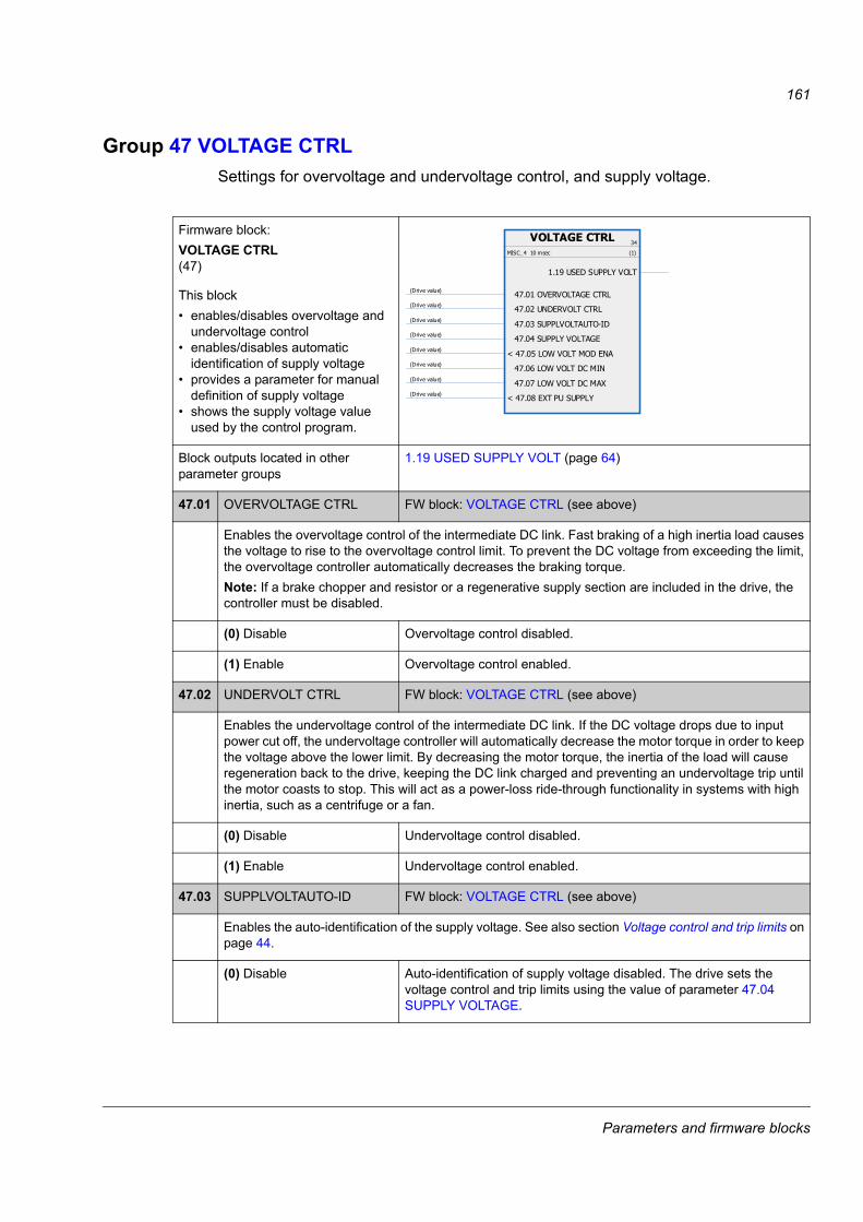
161
Group 47 VOLTAGE CTRLSettings for overvoltage and undervoltage control, and supply voltage.
47Firmware block:VOLTAGE CTRL(47)
This block• enables/disables overvoltage and
undervoltage control• enables/disables automatic
identification of supply voltage• provides a parameter for manual
definition of supply voltage• shows the supply voltage value
used by the control program.
Block outputs located in other parameter groups
1.19 USED SUPPLY VOLT (page 64)
47.01 OVERVOLTAGE CTRL FW block: VOLTAGE CTRL (see above)
Enables the overvoltage control of the intermediate DC link. Fast braking of a high inertia load causes the voltage to rise to the overvoltage control limit. To prevent the DC voltage from exceeding the limit, the overvoltage controller automatically decreases the braking torque.Note: If a brake chopper and resistor or a regenerative supply section are included in the drive, the controller must be disabled.
(0) Disable Overvoltage control disabled.
(1) Enable Overvoltage control enabled.
47.02 UNDERVOLT CTRL FW block: VOLTAGE CTRL (see above)
Enables the undervoltage control of the intermediate DC link. If the DC voltage drops due to input power cut off, the undervoltage controller will automatically decrease the motor torque in order to keep the voltage above the lower limit. By decreasing the motor torque, the inertia of the load will cause regeneration back to the drive, keeping the DC link charged and preventing an undervoltage trip until the motor coasts to stop. This will act as a power-loss ride-through functionality in systems with high inertia, such as a centrifuge or a fan.
(0) Disable Undervoltage control disabled.
(1) Enable Undervoltage control enabled.
47.03 SUPPLVOLTAUTO-ID FW block: VOLTAGE CTRL (see above)
Enables the auto-identification of the supply voltage. See also section Voltage control and trip limits on page 44.
(0) Disable Auto-identification of supply voltage disabled. The drive sets the voltage control and trip limits using the value of parameter 47.04 SUPPLY VOLTAGE.
VOLTAGE CTRL 34
MISC_4 10 msec (1)
47.01 OVERVOLTAGE CTRL(Drive value)
47.02 UNDERVOLT CTRL(Drive value)
47.03 SUPPLVOLTAUTO-ID(Drive value)
47.04 SUPPLY VOLTAGE(Drive value)
< 47.05 LOW VOLT MOD ENA(Drive value)
47.06 LOW VOLT DC MIN(Drive value)
47.07 LOW VOLT DC MAX(Drive value)
< 47.08 EXT PU SUPPLY(Drive value)
1.19 USED SUPPLY VOLT
Parameters and firmware blocks
162
(1) Enable Auto-identification of supply voltage enabled. The drive detects the supply voltage level during intermediate circuit charging and sets the voltage control and trip limits accordingly.
47.04 SUPPLY VOLTAGE FW block: VOLTAGE CTRL (see above)
Defines the nominal supply voltage. Used if auto-identification of the supply voltage is not enabled by parameter 47.03 SUPPLVOLTAUTO-ID.
0…1000 V Nominal supply voltage.
47.05 LOW VOLT MOD ENA FW block: None
Enables/disables (or selects a signal source that enables/disables) Low voltage mode. 0 = Low voltage mode disabled, 1 = Low voltage mode enabled. See section Low voltage mode on page 45.
Bit pointer: Group, index and bit
47.06 LOW VOLT DC MIN FW block: None
Minimum DC voltage for Low voltage mode. See section Low voltage mode on page 45.
250…450 V Minimum DC voltage for Low voltage mode.
47.07 LOW VOLT DC MAX FW block: None
Maximum DC voltage for Low voltage mode. See section Low voltage mode on page 45.Note: The value of this parameter must be higher than (47.06 LOW VOLT DC MIN + 50 V).
350…810 V Maximum DC voltage for Low voltage mode.
47.08 EXT PU SUPPLY FW block: None
Enables/disables (or selects a signal source that enables/disables) external power unit supply, used with low DC supply voltages such as a battery. 0 = External power unit supply disabled, 1 = External power unit supply enabled. See section Low voltage mode on page 45.
Bit pointer: Group, index and bit
Parameters and firmware blocks

163
Group 48 BRAKE CHOPPERConfiguration of internal brake chopper.
48Firmware block:BRAKE CHOPPER(48)
This block configures the brake chopper control and supervision.
48.01 BC ENABLE FW block: BRAKE CHOPPER (see above)
Enables the brake chopper control.Note: Before enabling brake chopper control, ensure the brake resistor is installed and the overvoltage control is switched off (parameter 47.01 OVERVOLTAGE CTRL). The drive has a built-in brake chopper.
(0) Disable Brake chopper control disabled.
(1) EnableTherm Enable brake chopper control with resistor overload protection.
(2) Enable Enable brake chopper control without resistor overload protection. This setting can be used, for example, if the resistor is equipped with a thermal circuit breaker that is wired to stop the drive if the resistor overheats.
48.02 BC RUN-TIME ENA FW block: BRAKE CHOPPER (see above)
Selects the source for quick run-time brake chopper control.0 = Brake chopper IGBT pulses are cut off.1 = Normal brake chopper IGBT modulation. The overvoltage control is automatically switched off.This parameter can be used to program the chopper control to function only when the drive is operating in generating mode.
Bit pointer: Group, index and bit
48.03 BRTHERMTIMECONST FW block: BRAKE CHOPPER (see above)
Defines the thermal time constant of the brake resistor for overload protection.
0…10000 s Brake resistor thermal time constant.
48.04 BR POWER MAX CNT FW block: BRAKE CHOPPER (see above)
Defines the maximum continuous braking power which will raise the resistor temperature to the maximum allowed value. The value is used in the overload protection.
0…10000 kW Maximum continuous braking power.
48.05 R BR FW block: BRAKE CHOPPER (see above)
Defines the resistance value of the brake resistor. The value is used for brake chopper protection.
BRAKE CHOPPER35
TLF10 2 msec (11)
48.01 BC ENABLE [ Disable ]
< 48.02 BC RUN-TIME ENA [ TRUE ]
48.03 BRTHERMTIMECONST [ 0 s ]
48.04 BR POWER MAX CNT [ 0.0000 kW ]
48.05 R BR [ 0.0000 Ohm ]
48.06 BR TEMP FAULTLIM [ 105 % ]
48.07 BR TEMP ALARMLIM [ 95 % ]
Parameters and firmware blocks
164
0.1…1000 ohm Resistance.
48.06 BR TEMP FAULTLIM FW block: BRAKE CHOPPER (see above)
Selects the fault limit for the brake resistor temperature supervision. The value is given in percent of the temperature the resistor reaches when loaded with the power defined by parameter 48.04 BR POWER MAX CNT.When the limit is exceeded the drive trips on fault BR OVERHEAT.
0…150% Resistor temperature fault limit.
48.07 BR TEMP ALARMLIM FW block: BRAKE CHOPPER (see above)
Selects the alarm limit for the brake resistor temperature supervision. The value is given in percent of the temperature the resistor reaches when loaded with the power defined by parameter 48.04 BR POWER MAX CNT.When limit is exceeded the drive generates alarm BR OVERHEAT.
0…150% Resistor temperature alarm limit.
Parameters and firmware blocks
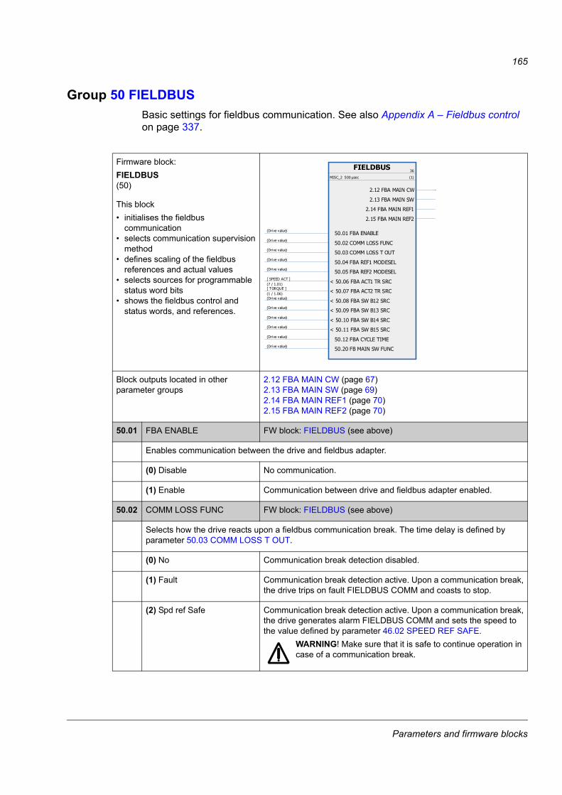
165
Group 50 FIELDBUSBasic settings for fieldbus communication. See also Appendix A – Fieldbus control on page 337.
50Firmware block:FIELDBUS(50)
This block• initialises the fieldbus
communication• selects communication supervision
method• defines scaling of the fieldbus
references and actual values• selects sources for programmable
status word bits• shows the fieldbus control and
status words, and references.
Block outputs located in other parameter groups
2.12 FBA MAIN CW (page 67)2.13 FBA MAIN SW (page 69)2.14 FBA MAIN REF1 (page 70)2.15 FBA MAIN REF2 (page 70)
50.01 FBA ENABLE FW block: FIELDBUS (see above)
Enables communication between the drive and fieldbus adapter.
(0) Disable No communication.
(1) Enable Communication between drive and fieldbus adapter enabled.
50.02 COMM LOSS FUNC FW block: FIELDBUS (see above)
Selects how the drive reacts upon a fieldbus communication break. The time delay is defined by parameter 50.03 COMM LOSS T OUT.
(0) No Communication break detection disabled.
(1) Fault Communication break detection active. Upon a communication break, the drive trips on fault FIELDBUS COMM and coasts to stop.
(2) Spd ref Safe Communication break detection active. Upon a communication break, the drive generates alarm FIELDBUS COMM and sets the speed to the value defined by parameter 46.02 SPEED REF SAFE.
WARNING! Make sure that it is safe to continue operation in case of a communication break.
FIELDBUS 36
MISC_2 500 μsec (1)
50.01 FBA ENABLE(Drive value)
50.02 COMM LOSS FUNC(Drive value)
50.03 COMM LOSS T OUT(Drive value)
50.04 FBA REF1 MODESEL(Drive value)
50.05 FBA REF2 MODESEL(Drive value)
< 50.06 FBA ACT1 TR SRC[ SPEED ACT ](7 / 1.01)
< 50.07 FBA ACT2 TR SRC[ TORQUE ](1 / 1.06)
< 50.08 FBA SW B12 SRC(Drive value)
< 50.09 FBA SW B13 SRC(Drive value)
< 50.10 FBA SW B14 SRC(Drive value)
< 50.11 FBA SW B15 SRC(Drive value)
50.12 FBA CYCLE TIME(Drive value)
50.20 FB MAIN SW FUNC(Drive value)
2.12 FBA MAIN CW
2.13 FBA MAIN SW
2.14 FBA MAIN REF1
2.15 FBA MAIN REF2
Parameters and firmware blocks
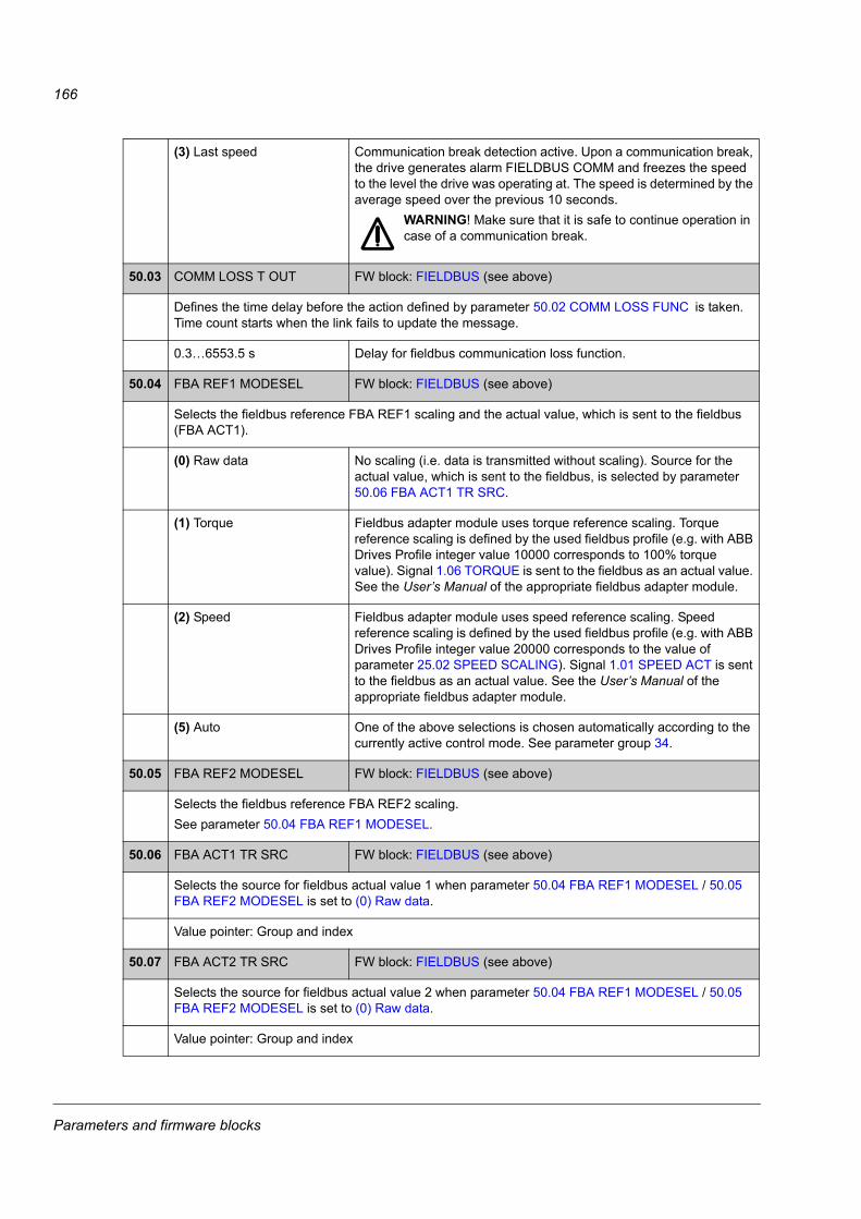
166
(3) Last speed Communication break detection active. Upon a communication break, the drive generates alarm FIELDBUS COMM and freezes the speed to the level the drive was operating at. The speed is determined by the average speed over the previous 10 seconds.
WARNING! Make sure that it is safe to continue operation in case of a communication break.
50.03 COMM LOSS T OUT FW block: FIELDBUS (see above)
Defines the time delay before the action defined by parameter 50.02 COMM LOSS FUNC is taken. Time count starts when the link fails to update the message.
0.3…6553.5 s Delay for fieldbus communication loss function.
50.04 FBA REF1 MODESEL FW block: FIELDBUS (see above)
Selects the fieldbus reference FBA REF1 scaling and the actual value, which is sent to the fieldbus (FBA ACT1).
(0) Raw data No scaling (i.e. data is transmitted without scaling). Source for the actual value, which is sent to the fieldbus, is selected by parameter 50.06 FBA ACT1 TR SRC.
(1) Torque Fieldbus adapter module uses torque reference scaling. Torque reference scaling is defined by the used fieldbus profile (e.g. with ABB Drives Profile integer value 10000 corresponds to 100% torque value). Signal 1.06 TORQUE is sent to the fieldbus as an actual value. See the User’s Manual of the appropriate fieldbus adapter module.
(2) Speed Fieldbus adapter module uses speed reference scaling. Speed reference scaling is defined by the used fieldbus profile (e.g. with ABB Drives Profile integer value 20000 corresponds to the value of parameter 25.02 SPEED SCALING). Signal 1.01 SPEED ACT is sent to the fieldbus as an actual value. See the User’s Manual of the appropriate fieldbus adapter module.
(5) Auto One of the above selections is chosen automatically according to the currently active control mode. See parameter group 34.
50.05 FBA REF2 MODESEL FW block: FIELDBUS (see above)
Selects the fieldbus reference FBA REF2 scaling. See parameter 50.04 FBA REF1 MODESEL.
50.06 FBA ACT1 TR SRC FW block: FIELDBUS (see above)
Selects the source for fieldbus actual value 1 when parameter 50.04 FBA REF1 MODESEL / 50.05 FBA REF2 MODESEL is set to (0) Raw data.
Value pointer: Group and index
50.07 FBA ACT2 TR SRC FW block: FIELDBUS (see above)
Selects the source for fieldbus actual value 2 when parameter 50.04 FBA REF1 MODESEL / 50.05 FBA REF2 MODESEL is set to (0) Raw data.
Value pointer: Group and index
Parameters and firmware blocks

167
50.08 FBA SW B12 SRC FW block: FIELDBUS (see above)
Selects the source for freely programmable fieldbus status word bit 28 (2.13 FBA MAIN SW bit 28). Note that this functionality may not be supported by the fieldbus communication profile.
Bit pointer: Group, index and bit
50.09 FBA SW B13 SRC FW block: FIELDBUS (see above)
Selects the source for freely programmable fieldbus status word bit 29 (2.13 FBA MAIN SW bit 29). Note that this functionality may not be supported by the fieldbus communication profile.
Bit pointer: Group, index and bit
50.10 FBA SW B14 SRC FW block: FIELDBUS (see above)
Selects the source for freely programmable fieldbus status word bit 30 (2.13 FBA MAIN SW bit 30). Note that this functionality may not be supported by the fieldbus communication profile.
Bit pointer: Group, index and bit
50.11 FBA SW B15 SRC FW block: FIELDBUS (see above)
Selects the source for freely programmable fieldbus status word bit 31 (2.13 FBA MAIN SW bit 31). Note that this functionality may not be supported by the fieldbus communication profile.
Bit pointer: Group, index and bit
50.12 FBA CYCLE TIME FW block: FIELDBUS (see above)
Selects the fieldbus communication speed. The default selection is (2) Fast. Lowering the speed reduces the CPU load. The table below shows the read/write intervals for cyclic and acyclic data with each parameter setting.
*Cyclic data consists of fieldbus CW and SW, Ref1 and Ref2, and Act1 and Act2.**Acyclic data consists of the parameter data mapped to parameter groups 52 and 53.
(0) Slow Slow speed selected.
(1) Normal Normal speed selected.
(2) Fast Fast speed selected.
Selection Cyclic* Acyclic*Slow 10 ms 10 msNormal 2 ms 10 msFast 500 us 2 ms
Parameters and firmware blocks
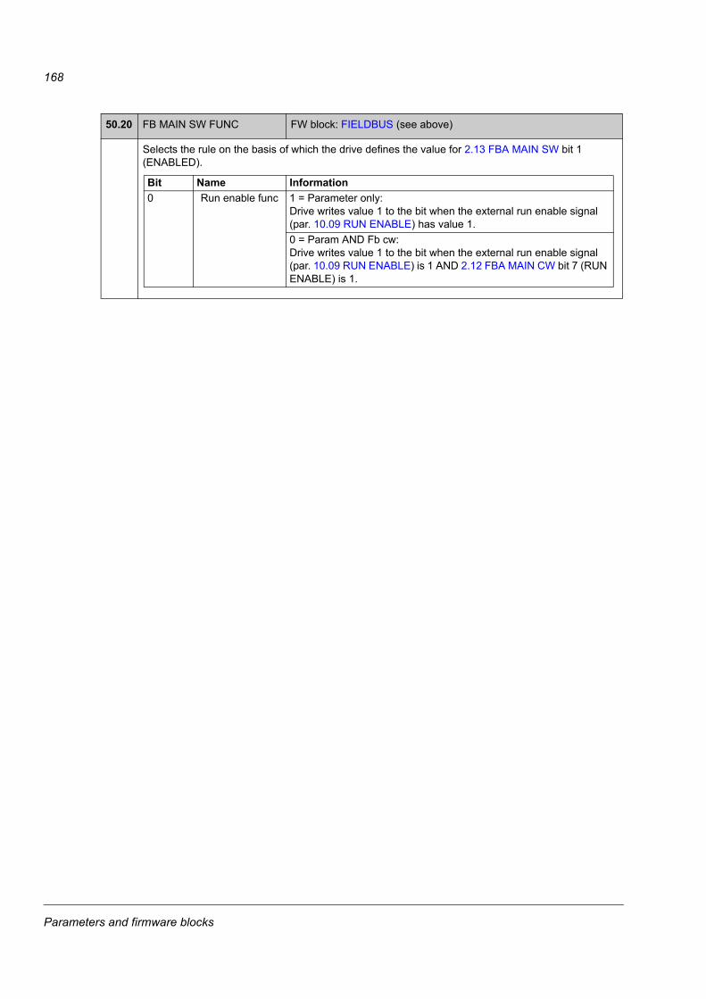
168
50.20 FB MAIN SW FUNC FW block: FIELDBUS (see above)
Selects the rule on the basis of which the drive defines the value for 2.13 FBA MAIN SW bit 1 (ENABLED).
Bit Name Information0 Run enable func 1 = Parameter only:
Drive writes value 1 to the bit when the external run enable signal (par. 10.09 RUN ENABLE) has value 1.0 = Param AND Fb cw:Drive writes value 1 to the bit when the external run enable signal (par. 10.09 RUN ENABLE) is 1 AND 2.12 FBA MAIN CW bit 7 (RUN ENABLE) is 1.
Parameters and firmware blocks
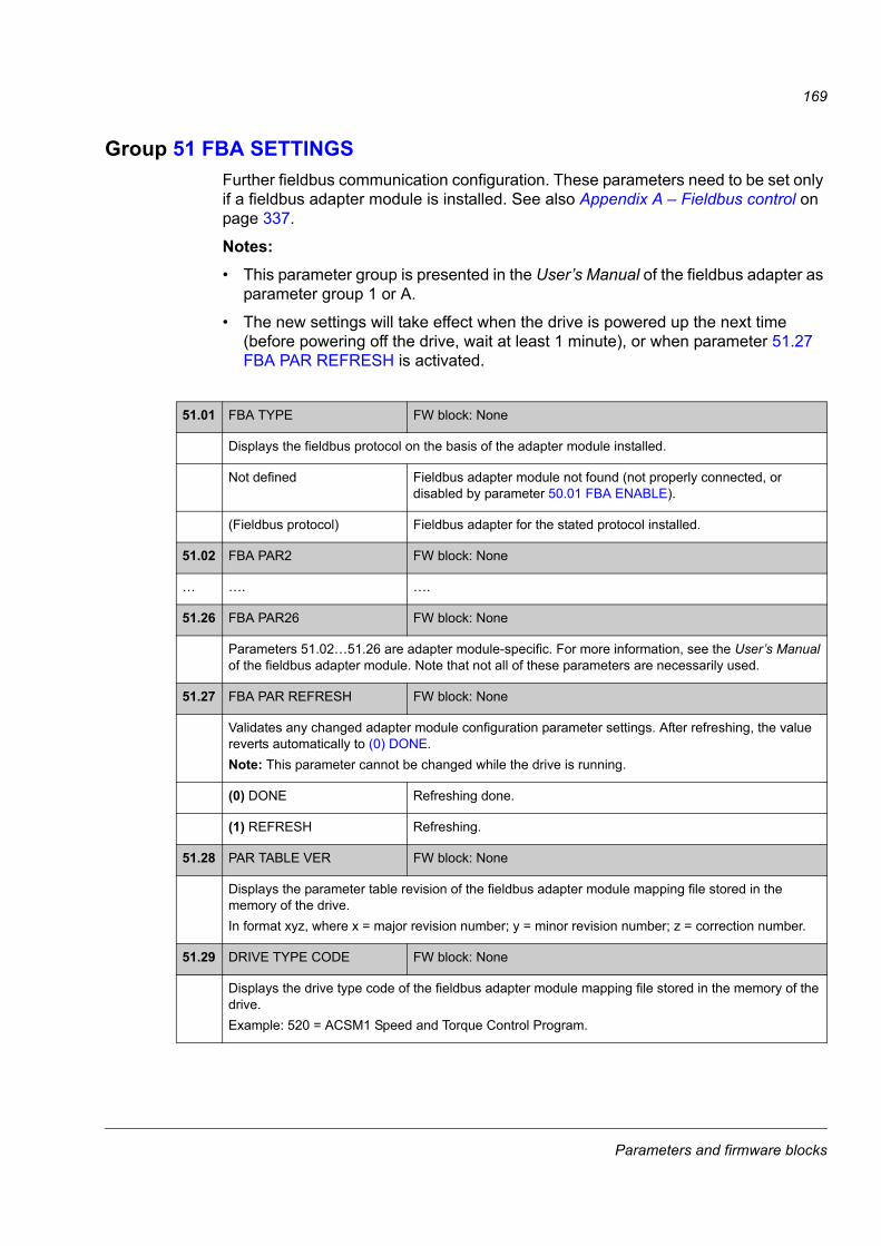
169
Group 51 FBA SETTINGSFurther fieldbus communication configuration. These parameters need to be set only if a fieldbus adapter module is installed. See also Appendix A – Fieldbus control on page 337.
Notes:• This parameter group is presented in the User’s Manual of the fieldbus adapter as
parameter group 1 or A.
• The new settings will take effect when the drive is powered up the next time (before powering off the drive, wait at least 1 minute), or when parameter 51.27 FBA PAR REFRESH is activated.
5151.01 FBA TYPE FW block: None
Displays the fieldbus protocol on the basis of the adapter module installed.
Not defined Fieldbus adapter module not found (not properly connected, or disabled by parameter 50.01 FBA ENABLE).
(Fieldbus protocol) Fieldbus adapter for the stated protocol installed.
51.02 FBA PAR2 FW block: None
… …. ….
51.26 FBA PAR26 FW block: None
Parameters 51.02…51.26 are adapter module-specific. For more information, see the User’s Manual of the fieldbus adapter module. Note that not all of these parameters are necessarily used.
51.27 FBA PAR REFRESH FW block: None
Validates any changed adapter module configuration parameter settings. After refreshing, the value reverts automatically to (0) DONE.Note: This parameter cannot be changed while the drive is running.
(0) DONE Refreshing done.
(1) REFRESH Refreshing.
51.28 PAR TABLE VER FW block: None
Displays the parameter table revision of the fieldbus adapter module mapping file stored in the memory of the drive.In format xyz, where x = major revision number; y = minor revision number; z = correction number.
51.29 DRIVE TYPE CODE FW block: None
Displays the drive type code of the fieldbus adapter module mapping file stored in the memory of the drive.Example: 520 = ACSM1 Speed and Torque Control Program.
Parameters and firmware blocks
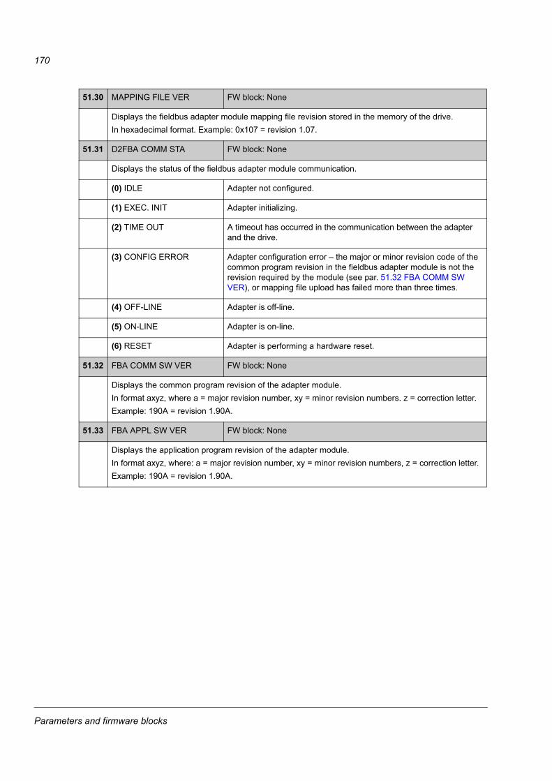
170
51.30 MAPPING FILE VER FW block: None
Displays the fieldbus adapter module mapping file revision stored in the memory of the drive. In hexadecimal format. Example: 0x107 = revision 1.07.
51.31 D2FBA COMM STA FW block: None
Displays the status of the fieldbus adapter module communication.
(0) IDLE Adapter not configured.
(1) EXEC. INIT Adapter initializing.
(2) TIME OUT A timeout has occurred in the communication between the adapter and the drive.
(3) CONFIG ERROR Adapter configuration error – the major or minor revision code of the common program revision in the fieldbus adapter module is not the revision required by the module (see par. 51.32 FBA COMM SW VER), or mapping file upload has failed more than three times.
(4) OFF-LINE Adapter is off-line.
(5) ON-LINE Adapter is on-line.
(6) RESET Adapter is performing a hardware reset.
51.32 FBA COMM SW VER FW block: None
Displays the common program revision of the adapter module.In format axyz, where a = major revision number, xy = minor revision numbers. z = correction letter.Example: 190A = revision 1.90A.
51.33 FBA APPL SW VER FW block: None
Displays the application program revision of the adapter module.In format axyz, where: a = major revision number, xy = minor revision numbers, z = correction letter.Example: 190A = revision 1.90A.
Parameters and firmware blocks
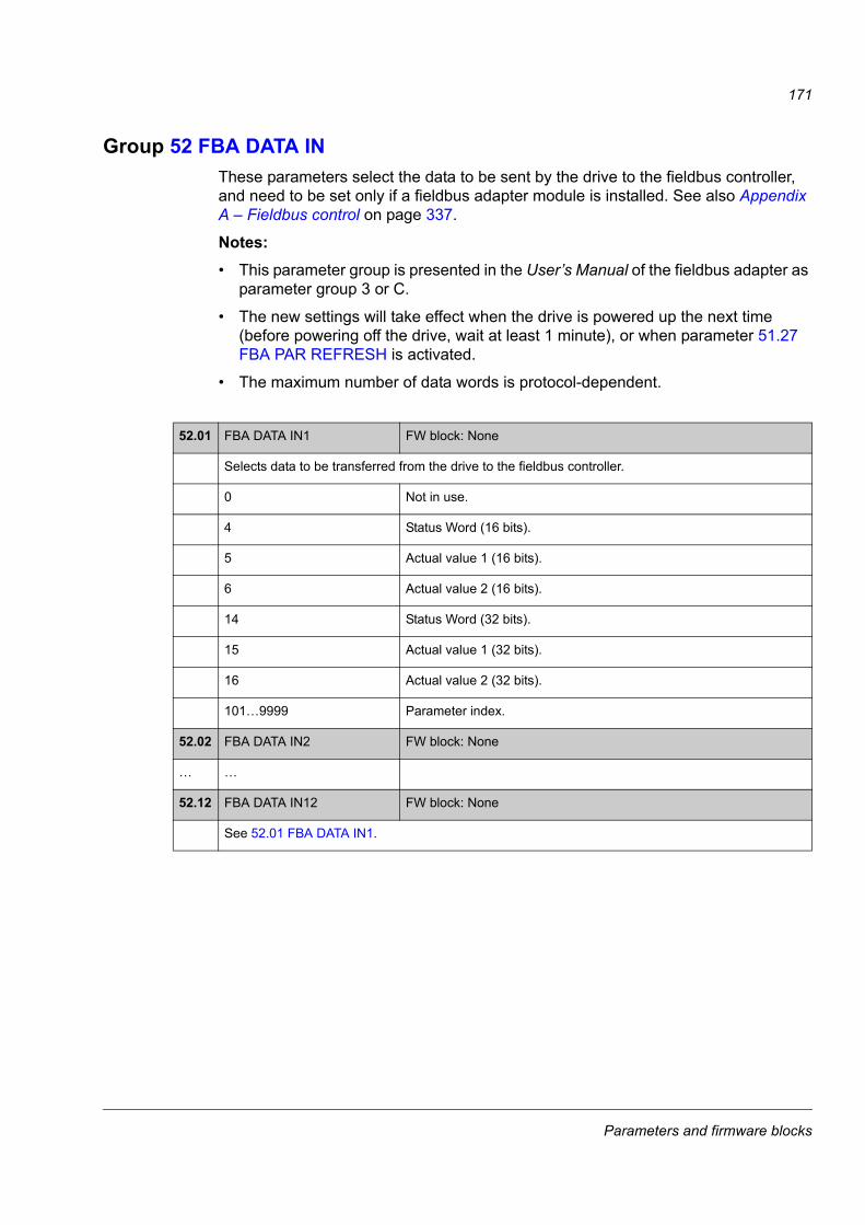
171
Group 52 FBA DATA INThese parameters select the data to be sent by the drive to the fieldbus controller, and need to be set only if a fieldbus adapter module is installed. See also Appendix A – Fieldbus control on page 337.
Notes:• This parameter group is presented in the User’s Manual of the fieldbus adapter as
parameter group 3 or C.
• The new settings will take effect when the drive is powered up the next time (before powering off the drive, wait at least 1 minute), or when parameter 51.27 FBA PAR REFRESH is activated.
• The maximum number of data words is protocol-dependent.
5252.01 FBA DATA IN1 FW block: None
Selects data to be transferred from the drive to the fieldbus controller.
0 Not in use.
4 Status Word (16 bits).
5 Actual value 1 (16 bits).
6 Actual value 2 (16 bits).
14 Status Word (32 bits).
15 Actual value 1 (32 bits).
16 Actual value 2 (32 bits).
101…9999 Parameter index.
52.02 FBA DATA IN2 FW block: None
… …
52.12 FBA DATA IN12 FW block: None
See 52.01 FBA DATA IN1.
Parameters and firmware blocks
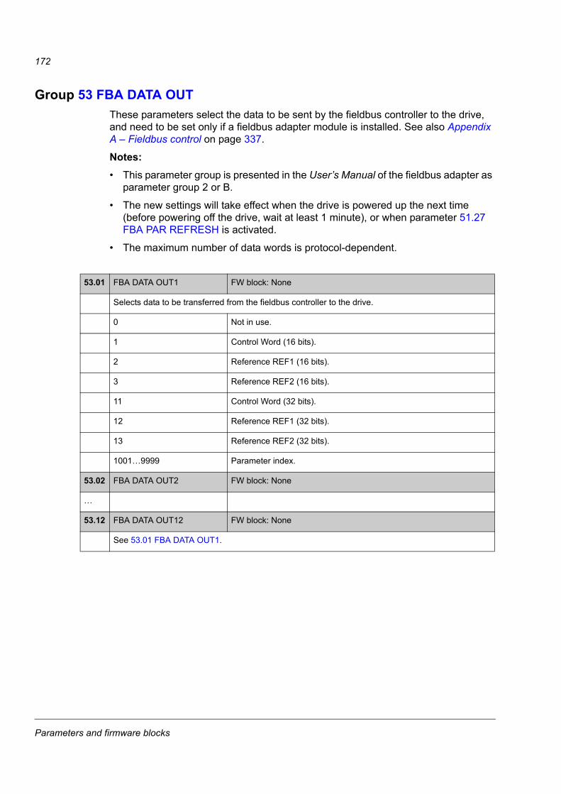
172
Group 53 FBA DATA OUTThese parameters select the data to be sent by the fieldbus controller to the drive, and need to be set only if a fieldbus adapter module is installed. See also Appendix A – Fieldbus control on page 337.
Notes:• This parameter group is presented in the User’s Manual of the fieldbus adapter as
parameter group 2 or B.
• The new settings will take effect when the drive is powered up the next time (before powering off the drive, wait at least 1 minute), or when parameter 51.27 FBA PAR REFRESH is activated.
• The maximum number of data words is protocol-dependent.
5353.01 FBA DATA OUT1 FW block: None
Selects data to be transferred from the fieldbus controller to the drive.
0 Not in use.
1 Control Word (16 bits).
2 Reference REF1 (16 bits).
3 Reference REF2 (16 bits).
11 Control Word (32 bits).
12 Reference REF1 (32 bits).
13 Reference REF2 (32 bits).
1001…9999 Parameter index.
53.02 FBA DATA OUT2 FW block: None
…
53.12 FBA DATA OUT12 FW block: None
See 53.01 FBA DATA OUT1.
Parameters and firmware blocks
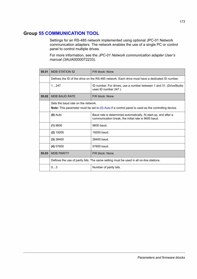
173
Group 55 COMMUNICATION TOOLSettings for an RS-485 network implemented using optional JPC-01 Network communication adapters. The network enables the use of a single PC or control panel to control multiple drives.
For more information, see the JPC-01 Network communication adapter User’s manual (3AUA0000072233).
5555.01 MDB STATION ID FW block: None
Defines the ID of the drive on the RS-485 network. Each drive must have a dedicated ID number.
1…247 ID number. For drives, use a number between 1 and 31. (DriveStudio uses ID number 247.)
55.02 MDB BAUD RATE FW block: None
Sets the baud rate on the network.Note: This parameter must be set to (0) Auto if a control panel is used as the controlling device.
(0) Auto Baud rate is determined automatically. At start-up, and after a communication break, the initial rate is 9600 baud.
(1) 9600 9600 baud.
(2) 19200 19200 baud.
(3) 38400 38400 baud.
(4) 57600 57600 baud.
55.03 MDB PARITY FW block: None
Defines the use of parity bits. The same setting must be used in all on-line stations.
0…3 Number of parity bits.
Parameters and firmware blocks
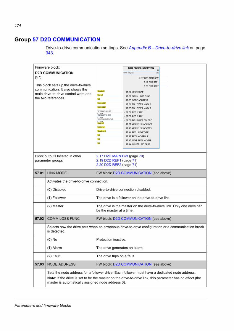
174
Group 57 D2D COMMUNICATIONDrive-to-drive communication settings. See Appendix B – Drive-to-drive link on page 343.
57Firmware block:D2D COMMUNICATION(57)
This block sets up the drive-to-drive communication. It also shows the main drive-to-drive control word and the two references.
Block outputs located in other parameter groups
2.17 D2D MAIN CW (page 70)2.19 D2D REF1 (page 71)2.20 D2D REF2 (page 71)
57.01 LINK MODE FW block: D2D COMMUNICATION (see above)
Activates the drive-to-drive connection.
(0) Disabled Drive-to-drive connection disabled.
(1) Follower The drive is a follower on the drive-to-drive link.
(2) Master The drive is the master on the drive-to-drive link. Only one drive can be the master at a time.
57.02 COMM LOSS FUNC FW block: D2D COMMUNICATION (see above)
Selects how the drive acts when an erroneous drive-to-drive configuration or a communication break is detected.
(0) No Protection inactive.
(1) Alarm The drive generates an alarm.
(2) Fault The drive trips on a fault.
57.03 NODE ADDRESS FW block: D2D COMMUNICATION (see above)
Sets the node address for a follower drive. Each follower must have a dedicated node address.Note: If the drive is set to be the master on the drive-to-drive link, this parameter has no effect (the master is automatically assigned node address 0).
D2D COMMUNICATION44
TLF9 500 μsec (2)
57.01 LINK MODE [ Disabled ]
57.02 COMM LOSS FUNC [ Alarm ]
57.03 NODE ADDRESS [ 1 ]
57.04 FOLLOWER MASK 1 [ 0000 0000 ]
57.05 FOLLOWER MASK 2 [ 0000 0000 ]
< 57.06 REF 1 SRC[ SPEEDREF RAMPED ](6 / 3.04)
< 57.07 REF 2 SRC[ TORQ REF TO TC ](8 / 3.13)
< 57.08 FOLLOWER CW SRC[ D2D FOLLOWER CW ](4 / 2.18)
57.09 KERNEL SYNC MODE [ NoSync ]
57.10 KERNEL SYNC OFFS [ 0.000 ms ]
57.11 REF 1 MSG TYPE [ Broadcast ]
57.12 REF1 MC GROUP [ 0 ]
57.13 NEXT REF1 MC GRP [ 0 ]
57.14 NR REF1 MC GRPS [ 1 ]
2.17 D2D MAIN CW
2.19 D2D REF1
2.20 D2D REF2
Parameters and firmware blocks

175
1…62 Node address.
57.04 FOLLOWER MASK 1 FW block: D2D COMMUNICATION (see above)
On the master drive, selects the followers to be polled. If no response is received from a polled follower, the action selected by parameter 57.02 COMM LOSS FUNC is taken.The least significant bit represents follower with node address 1, while the most significant bit represents follower 31. When a bit is set to 1, the corresponding node address is polled. For example, followers 1 and 2 are polled when this parameter is set to the value of 0x3.
0x00000000…0x7FFFFFFF Follower mask 1.
57.05 FOLLOWER MASK 2 FW block: D2D COMMUNICATION (see above)
On the master drive, selects the followers to be polled. If no response is received from a polled follower, the action selected by parameter 57.02 COMM LOSS FUNC is taken.The least significant bit represents follower with node address 32, while the most significant bit represents follower 62. When a bit is set to 1, the corresponding node address is polled. For example, followers 32 and 33 are polled when this parameter is set to the value of 0x3.
0x00000000…0x7FFFFFFF Follower mask 2.
57.06 REF 1 SRC FW block: D2D COMMUNICATION (see above)
Selects the source of D2D reference 1 sent to the followers. The parameter is effective on the master drive, as well as submasters (57.03 NODE ADDRESS = 57.12 REF1 MC GROUP) in a multicast message chain (see parameter 57.11 REF 1 MSG TYPE).The default value is P.03.04, i.e. 3.04 SPEEDREF RAMPED.
Value pointer: Group and index.
57.07 REF 2 SRC FW block: D2D COMMUNICATION (see above)
On the master drive, selects the source of D2D reference 2 broadcast to all followers.The default value is P.03.13, i.e. 3.13 TORQ REF TO TC.
Value pointer: Group and index.
57.08 FOLLOWER CW SRC FW block: D2D COMMUNICATION (see above)
Selects the source of the D2D control word sent to the followers. The parameter is effective on the master drive, as well as submasters in a multicast message chain (see parameter 57.11 REF 1 MSG TYPE).The default value is P.02.18, i.e. 2.18 D2D FOLLOWER CW.
Value pointer: Group and index.
57.09 KERNEL SYNC MODE FW block: D2D COMMUNICATION (see above)
Determines which signal the time levels of the drive are synchronised with. An offset can be defined by parameter 57.10 KERNEL SYNC OFFS if desired.
(0) NoSync No synchronisation.
(1) D2DSync If the drive is the master on a drive-to-drive link, it broadcasts a synchronisation signal to the follower(s). If the drive is a follower, it synchronises its firmware time levels to the signal received from the master.
Parameters and firmware blocks
176
(2) FBSync The drive synchronises its firmware time levels to a synchronisation signal received through a fieldbus adapter.
(3) FBToD2DSync If the drive is the master on a drive-to-drive link, it synchronises its firmware time levels to a synchronisation signal received from a fieldbus adapter, and broadcasts the signal on the drive-to-drive link. If the drive is a follower, this setting has no effect.
57.10 KERNEL SYNC OFFS FW block: D2D COMMUNICATION (see above)
Defines an offset between the synchronisation signal received and the time levels of the drive. With a positive value, the drive time levels will lag behind the synchronisation signal; with a negative value, the drive time levels will lead.
-4999…5000 ms Synchronisation offset.
57.11 REF 1 MSG TYPE FW block: D2D COMMUNICATION (see above)
By default, in drive-to-drive communication, the master broadcasts the drive-to-drive control word and references 1 and 2 to all followers. This parameter enables multicasting, i.e. sending the drive-to-drive control word and reference 1 to a certain drive or group of drives. The message can then be further relayed to another group of drives to form a multicast chain.In the master, as well as any submaster (i.e. follower relaying the message to other followers), the sources for the control word and reference 1 are selected by parameters 57.08 FOLLOWER CW SRC and 57.06 REF 1 SRC respectively.Note: Reference 2 is broadcast by the master to all followers.For more information, see Appendix B – Drive-to-drive link on page 343.
(0) Broadcast The control word and reference 1 are sent by the master to all followers. If the master has this setting, the parameter has no effect in the followers.
(1) Ref1 MC Grps The drive-to-drive control word and reference 1 are only sent to the drives in the multicast group specified by parameter 57.13 NEXT REF1 MC GRP. This setting can also be used in submasters (followers in which parameters 57.03 NODE ADDRESS and 57.12 REF1 MC GROUP are set to the same value) to form a multicast chain.
57.12 REF1 MC GROUP FW block: D2D COMMUNICATION (see above)
Selects the multicast group the drive belongs to. See parameter 57.11 REF 1 MSG TYPE.
0…62 Multicast group (0 = none).
57.13 NEXT REF1 MC GRP FW block: D2D COMMUNICATION (see above)
Specifies the next multicast group of drives the multicast message is relayed to. See parameter 57.11 REF 1 MSG TYPE. This parameter is effective only in the master or in submasters (followers in which parameters 57.03 NODE ADDRESS and 57.12 REF1 MC GROUP are set to the same value).
0…62 Next multicast group in message chain.
Parameters and firmware blocks
177
57.14 NR REF1 MC GRPS FW block: D2D COMMUNICATION (see above)
Sets the number of drives sending messages in the message chain. The value is typically equal to the number of multicast groups in the chain assuming that the last drive is NOT sending an acknowledgement to the master. See parameter 57.11 REF 1 MSG TYPE.Notes:• This parameter is only effective in the master.
1…62 Total number of links in multicast message chain.
57.15 D2D COMM PORT FW block: None
Defines the hardware to which the drive-to-drive link is connected. In special cases (such as harsh operating conditions), the galvanic isolation provided by the RS-485 interface of the FMBA module may make for more robust communication than the standard drive-to-drive connection.
(0) on-board Connector X5 on the JCU Control Unit is used.
(1) Slot 1 An FMBA module installed in JCU option slot 1 is used.
(2) Slot 2 An FMBA module installed in JCU option slot 2 is used.
(3) Slot 3 An FMBA module installed in JCU option slot 3 is used.
Parameters and firmware blocks
178
Group 90 ENC MODULE SELSettings for encoder activation, emulation, TTL echo, and encoder cable fault detection.
The firmware supports two encoders, encoder 1 and 2 (but only one FEN-21 Resolver Interface Module). Revolution counting is only supported for encoder 1. The following optional interface modules are available:
• TTL Encoder Interface Module FEN-01: two TTL inputs, TTL output (for encoder emulation and echo), two digital inputs for position latching, PTC temperature sensor connection
• Absolute Encoder Interface FEN-11: absolute encoder input, TTL input, TTL output (for encoder emulation and echo), two digital inputs for position latching, PTC/KTY temperature sensor connection
• Resolver Interface Module FEN-21: resolver input, TTL input, TTL output (for encoder emulation echo), two digital inputs for position latching, PTC/KTY temperature sensor connection
• HTL Encoder Interface Module FEN-31: HTL encoder input, TTL output (for encoder emulation and echo), two digital inputs for position latching, PTC/KTY temperature sensor connection.
The interface module is connected to drive option Slot 1 or 2. Note: Two encoder interface modules of the same type are not allowed.
For encoder/resolver configuration, see parameter groups 91 (page 183), 92 (page 188) and 93 (page 189).
Note: Configuration data is written into the logic registers of the interface module once after the power-up. If parameter values are changed, save values into the permanent memory using parameter 16.07 PARAM SAVE. The new settings will take effect when the drive is powered up again, or after re-configuration is forced using parameter 90.10 ENC PAR REFRESH.
Parameters and firmware blocks
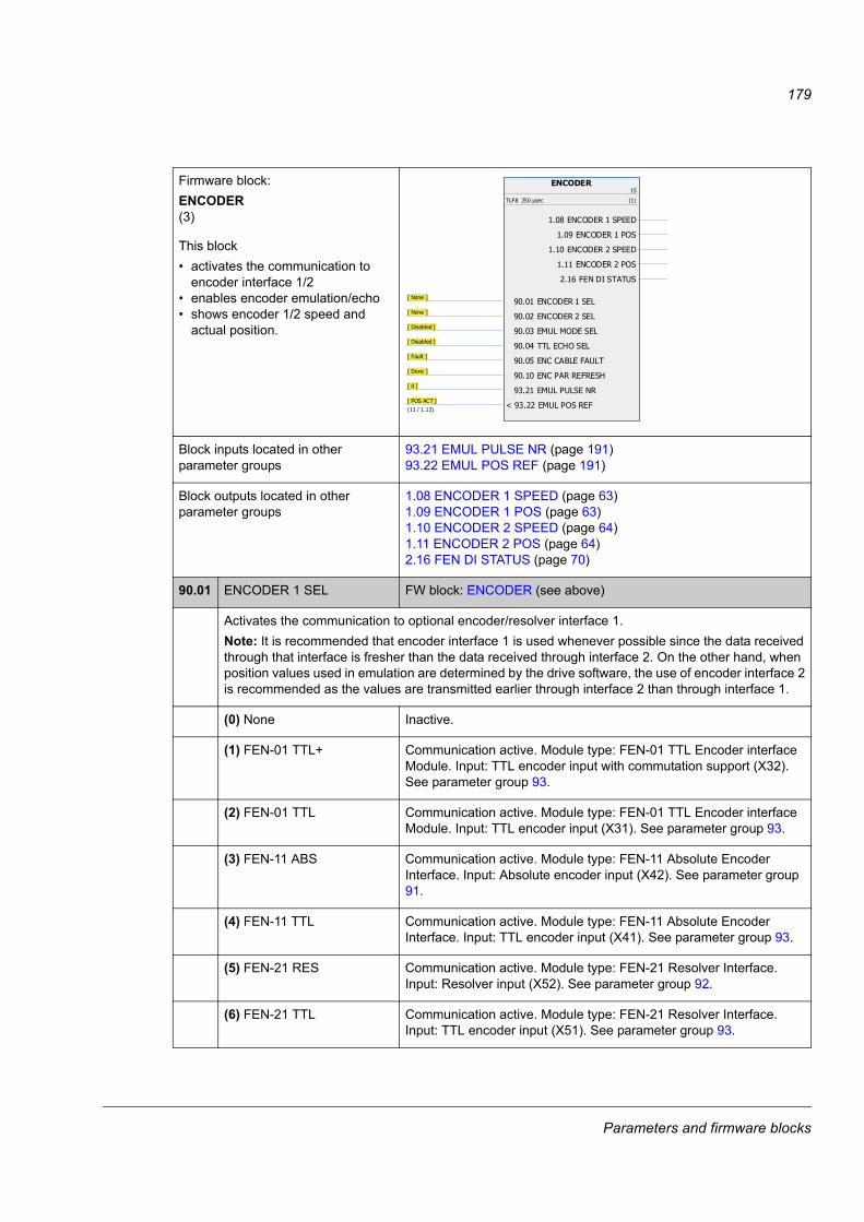
179
90Firmware block:ENCODER(3)
This block• activates the communication to
encoder interface 1/2• enables encoder emulation/echo• shows encoder 1/2 speed and
actual position.
Block inputs located in other parameter groups
93.21 EMUL PULSE NR (page 191)93.22 EMUL POS REF (page 191)
Block outputs located in other parameter groups
1.08 ENCODER 1 SPEED (page 63)1.09 ENCODER 1 POS (page 63)1.10 ENCODER 2 SPEED (page 64)1.11 ENCODER 2 POS (page 64)2.16 FEN DI STATUS (page 70)
90.01 ENCODER 1 SEL FW block: ENCODER (see above)
Activates the communication to optional encoder/resolver interface 1.Note: It is recommended that encoder interface 1 is used whenever possible since the data received through that interface is fresher than the data received through interface 2. On the other hand, when position values used in emulation are determined by the drive software, the use of encoder interface 2 is recommended as the values are transmitted earlier through interface 2 than through interface 1.
(0) None Inactive.
(1) FEN-01 TTL+ Communication active. Module type: FEN-01 TTL Encoder interface Module. Input: TTL encoder input with commutation support (X32). See parameter group 93.
(2) FEN-01 TTL Communication active. Module type: FEN-01 TTL Encoder interface Module. Input: TTL encoder input (X31). See parameter group 93.
(3) FEN-11 ABS Communication active. Module type: FEN-11 Absolute Encoder Interface. Input: Absolute encoder input (X42). See parameter group 91.
(4) FEN-11 TTL Communication active. Module type: FEN-11 Absolute Encoder Interface. Input: TTL encoder input (X41). See parameter group 93.
(5) FEN-21 RES Communication active. Module type: FEN-21 Resolver Interface. Input: Resolver input (X52). See parameter group 92.
(6) FEN-21 TTL Communication active. Module type: FEN-21 Resolver Interface. Input: TTL encoder input (X51). See parameter group 93.
ENCODER15
TLF8 250 μsec (1)
90.01 ENCODER 1 SEL [ None ]
90.02 ENCODER 2 SEL [ None ]
90.03 EMUL MODE SEL [ Disabled ]
90.04 TTL ECHO SEL [ Disabled ]
90.05 ENC CABLE FAULT [ Fault ]
90.10 ENC PAR REFRESH [ Done ]
93.21 EMUL PULSE NR [ 0 ]
< 93.22 EMUL POS REF [ POS ACT ](11 / 1.12)
1.08 ENCODER 1 SPEED
1.09 ENCODER 1 POS
1.10 ENCODER 2 SPEED
1.11 ENCODER 2 POS
2.16 FEN DI STATUS
Parameters and firmware blocks
180
(7) FEN-31 HTL Communication active. Module type: FEN-31 HTL Encoder Interface. Input: HTL encoder input (X82). See parameter group 93.
90.02 ENCODER 2 SEL FW block: ENCODER (see above)
Activates the communication to the optional encoder/resolver interface 2.For selections, see parameter 90.01 ENCODER 1 SEL.Note: The counting of full shaft revolutions is not supported for encoder 2.
90.03 EMUL MODE SEL FW block: ENCODER (see above)
Enables the encoder emulation and selects the position value and the TTL output used in the emulation process.In encoder emulation, a calculated position difference is transformed to a corresponding number of TTL pulses to be transmitted via the TTL output. The position difference is the difference between the latest and the previous position values.The position value used in emulation can be either a position determined by the drive software or a position measured by an encoder. If drive software position is used, the source for the used position is selected by parameter 93.22 EMUL POS REF. Because the software causes a delay, it is recommended that actual position is always taken from an encoder. Drive software is recommended to be used only with position reference emulation.Encoder emulation can be used to increase or decrease the pulse number when TTL encoder data is transmitted via the TTL output e.g. to another drive. If the pulse number requires no alternation, use encoder echo for data transformation. See parameter 90.04 TTL ECHO SEL. Note: If encoder emulation and echo are enabled for the same FEN-xx TTL output, the emulation overrides the echo.If an encoder input is selected as emulation source, the corresponding selection must be activated either with parameter 90.01 ENCODER 1 SEL or 90.02 ENCODER 2 SEL.The TTL encoder pulse number used in emulation must be defined by parameter 93.21 EMUL PULSE NR. See parameter group 93.
(0) Disabled Emulation disabled.
(1) FEN-01 SWref Module type: FEN-01 TTL Encoder interface Module. Emulation: Drive software position (source selected by par. 93.22 EMUL POS REF) is emulated to FEN-01 TTL output.
(2) FEN-01 TTL+ Module type: FEN-01 TTL Encoder interface Module. Emulation: FEN-01 TTL encoder input (X32) position is emulated to FEN-01 TTL output.
(3) FEN-01 TTL Module type: FEN-01 TTL Encoder interface Module. Emulation: FEN-01 TTL encoder input (X31) position is emulated to FEN-01 TTL output.
(4) FEN-11 SWref Module type: FEN-11 Absolute Encoder Interface. Emulation: Drive software position (source selected by par. 93.22 EMUL POS REF) is emulated to FEN-11 TTL output.
(5) FEN-11 ABS Module type: FEN-11 Absolute Encoder Interface. Emulation: FEN-11 absolute encoder input (X42) position is emulated to FEN-11 TTL output.
(6) FEN-11 TTL Module type: FEN-11 Absolute Encoder Interface. Emulation: FEN-11 TTL encoder input (X41) position is emulated to FEN-11 TTL output.
Parameters and firmware blocks

181
(7) FEN-21 SWref Module type: FEN-21 Resolver Interface. Emulation: Drive software position (source selected by par. 93.22 EMUL POS REF) is emulated to FEN-21 TTL output.
(8) FEN-21 RES Module type: FEN-21 Resolver Interface. Emulation: FEN-21 resolver input (X52) position is emulated to FEN-21 TTL output.
(9) FEN-21 TTL Module type: FEN-21 Resolver Interface. Emulation: FEN-21 TTL encoder input (X51) position is emulated to FEN-21 TTL output.
(10) FEN-31 SWref Module type: FEN-31 HTL Encoder Interface. Emulation: Drive software position (source selected by par. 93.22 EMUL POS REF) is emulated to FEN-31 TTL output.
(11) FEN-31 HTL Module type: FEN-31 HTL Encoder Interface. Emulation: FEN-31 HTL encoder input (X82) position is emulated to FEN-31 TTL output.
90.04 TTL ECHO SEL FW block: ENCODER (see above)
Enables and selects the interface for the TTL encoder signal echo.Note: If encoder emulation and echo are enabled for the same FEN-xx TTL output, the emulation overrides the echo.
(0) Disabled TTL echo disabled.
(1) FEN-01 TTL+ Module type: FEN-01 TTL Encoder Interface. Echo: TTL encoder input (X32) pulses are echoed to the TTL output.
(2) FEN-01 TTL Module type: FEN-01 TTL Encoder Interface. Echo: TTL encoder input (X31) pulses are echoed to the TTL output.
(3) FEN-11 TTL Module type: FEN-11 Absolute Encoder Interface. Echo: TTL encoder input (X41) pulses are echoed to the TTL output.
(4) FEN-21 TTL Module type: FEN-21 Resolver Interface. Echo: TTL encoder input (X51) pulses are echoed to the TTL output.
(5) FEN-31 HTL Module type: FEN-31 HTL Encoder Interface. Echo: HTL encoder input (X82) pulses are echoed to the TTL output.
90.05 ENC CABLE FAULT FW block: ENCODER (see above)
Selects the action in case an encoder cable fault is detected by the FEN-xx encoder interface.Notes:• This functionality is only available with the absolute encoder input of the FEN-11 based on sine/
cosine incremental signals, and with the HTL input of the FEN-31.• When the encoder input is used for speed feedback (see 22.01 SPEED FB SEL), this parameter
may be overridden by parameter 22.09 SPEED FB FAULT.
(0) No Cable fault detection inactive.
(1) Fault The drive trips on an ENCODER 1/2 CABLE fault.
Parameters and firmware blocks
182
(2) Warning The drive generates an ENCODER 1/2 CABLE warning. This is the recommended setting if the maximum pulse frequency of sine/cosine incremental signals exceeds 100 kHz; at high frequencies, the signals may attenuate enough to invoke the function. The maximum pulse frequency can be calculated as follows:
90.10 ENC PAR REFRESH FW block: ENCODER (see above)
Setting this parameter to 1 forces a reconfiguration of the FEN-xx interfaces, which is needed for any parameter changes in groups 90…93 to take effect.Note: This parameter cannot be changed while the drive is running.
(0) Done Refreshing done.
(1) Configure Reconfigure. The value will automatically revert to DONE.
Pulses per revolution (par. 91.01) × Maximum speed in rpm60
Parameters and firmware blocks
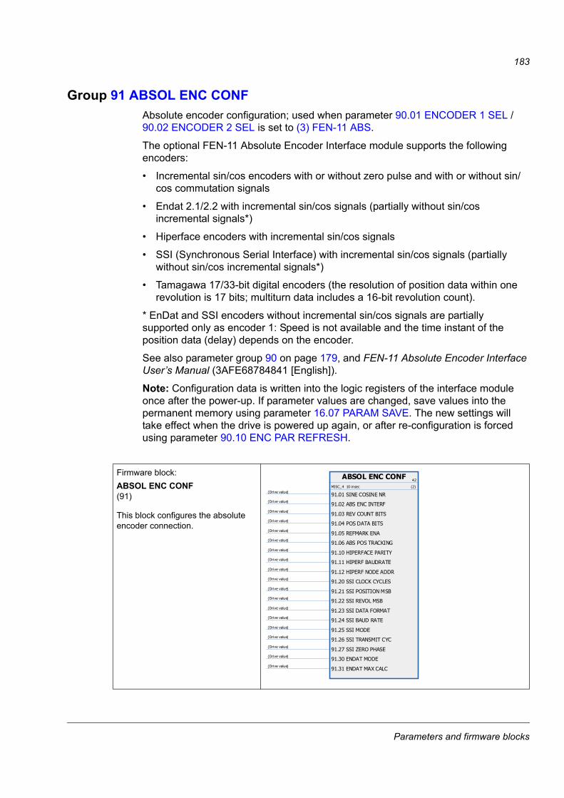
183
Group 91 ABSOL ENC CONFAbsolute encoder configuration; used when parameter 90.01 ENCODER 1 SEL /90.02 ENCODER 2 SEL is set to (3) FEN-11 ABS.
The optional FEN-11 Absolute Encoder Interface module supports the following encoders:
• Incremental sin/cos encoders with or without zero pulse and with or without sin/cos commutation signals
• Endat 2.1/2.2 with incremental sin/cos signals (partially without sin/cos incremental signals*)
• Hiperface encoders with incremental sin/cos signals
• SSI (Synchronous Serial Interface) with incremental sin/cos signals (partially without sin/cos incremental signals*)
• Tamagawa 17/33-bit digital encoders (the resolution of position data within one revolution is 17 bits; multiturn data includes a 16-bit revolution count).
* EnDat and SSI encoders without incremental sin/cos signals are partially supported only as encoder 1: Speed is not available and the time instant of the position data (delay) depends on the encoder.
See also parameter group 90 on page 179, and FEN-11 Absolute Encoder Interface User’s Manual (3AFE68784841 [English]).
Note: Configuration data is written into the logic registers of the interface module once after the power-up. If parameter values are changed, save values into the permanent memory using parameter 16.07 PARAM SAVE. The new settings will take effect when the drive is powered up again, or after re-configuration is forced using parameter 90.10 ENC PAR REFRESH.
91Firmware block:ABSOL ENC CONF(91)
This block configures the absolute encoder connection.
ABSOL ENC CONF 42
MISC_4 10 msec (2)
91.01 SINE COSINE NR(Drive value)
91.02 ABS ENC INTERF(Drive value)
91.03 REV COUNT BITS(Drive value)
91.04 POS DATA BITS(Drive value)
91.05 REFMARK ENA(Drive value)
91.06 ABS POS TRACKING(Drive value)
91.10 HIPERFACE PARITY(Drive value)
91.11 HIPERF BAUDRATE(Drive value)
91.12 HIPERF NODE ADDR(Drive value)
91.20 SSI CLOCK CYCLES(Drive value)
91.21 SSI POSITION MSB(Drive value)
91.22 SSI REVOL MSB(Drive value)
91.23 SSI DATA FORMAT(Drive value)
91.24 SSI BAUD RATE(Drive value)
91.25 SSI MODE(Drive value)
91.26 SSI TRANSMIT CYC(Drive value)
91.27 SSI ZERO PHASE(Drive value)
91.30 ENDAT MODE(Drive value)
91.31 ENDAT MAX CALC(Drive value)
Parameters and firmware blocks
184
91.01 SINE COSINE NR FW block: ABSOL ENC CONF (see above)
Defines the number of sine/cosine wave cycles within one revolution.Note: This parameter does not need to be set when EnDat or SSI encoders are used in continuous mode. See parameter 91.25 SSI MODE / 91.30 ENDAT MODE.
0…65535 Number of sine/cosine wave cycles within one revolution.
91.02 ABS ENC INTERF FW block: ABSOL ENC CONF (see above)
Selects the source for the encoder absolute position.
(0) None Not selected.
(1) Commut sig Commutation signals.
(2) EnDat Serial interface: EnDat encoder.
(3) Hiperface Serial interface: HIPERFACE encoder.
(4) SSI Serial interface: SSI encoder.
(5) Tamag. 17/33B Serial interface: Tamagawa 17/33-bit encoder.
91.03 REV COUNT BITS FW block: ABSOL ENC CONF (see above)
Defines the number of bits used in revolution counting with multiturn encoders. Used when parameter 91.02 ABS ENC INTERF is set to (2) EnDat, (3) Hiperface or (4) SSI. When 91.02 ABS ENC INTERF is set to (5) Tamag. 17/33B), setting this parameter to a non-zero value activates multiturn data requesting.
0…32 Number of bits used in revolution count. E.g. 4096 revolutions => 12 bits.
91.04 POS DATA BITS FW block: ABSOL ENC CONF (see above)
Defines the number of bits used within one revolution when parameter 91.02 ABS ENC INTERF is set to (2) EnDat, (3) Hiperface or (4) SSI. When 91.02 ABS ENC INTERF is set to (5) Tamag. 17/33B, this parameter is internally set to 17.
0…32 Number of bits used within one revolution. E.g. 32768 positions per revolution => 15 bits.
91.05 REFMARK ENA FW block: ABSOL ENC CONF (see above)
Enables the encoder zero pulse for the absolute encoder input (X42) of an FEN-11 module (if present). Zero pulse can be used for position latching.Note: With serial interfaces (i.e. when parameter 91.02 ABS ENC INTERF is set to (2) EnDat, (3) Hiperface, (4) SSI or (5) Tamag. 17/33B), the zero pulse does not exist.
(0) FALSE Zero pulse disabled.
(1) TRUE Zero pulse enabled.
Parameters and firmware blocks
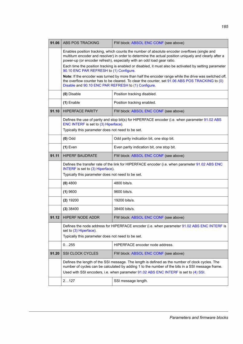
185
91.06 ABS POS TRACKING FW block: ABSOL ENC CONF (see above)
Enables position tracking, which counts the number of absolute encoder overflows (single and multiturn encoder and resolver) in order to determine the actual position uniquely and clearly after a power-up (or encoder refresh), especially with an odd load gear ratio.Each time the position tracking is enabled or disabled, it must also be activated by setting parameter 90.10 ENC PAR REFRESH to (1) Configure. Note: If the encoder was turned by more than half the encoder range while the drive was switched off, the overflow counter has to be cleared. To clear the counter, set 91.06 ABS POS TRACKING to (0) Disable and 90.10 ENC PAR REFRESH to (1) Configure.
(0) Disable Position tracking disabled.
(1) Enable Position tracking enabled.
91.10 HIPERFACE PARITY FW block: ABSOL ENC CONF (see above)
Defines the use of parity and stop bit(s) for HIPERFACE encoder (i.e. when parameter 91.02 ABS ENC INTERF is set to (3) Hiperface).Typically this parameter does not need to be set.
(0) Odd Odd parity indication bit, one stop bit.
(1) Even Even parity indication bit, one stop bit.
91.11 HIPERF BAUDRATE FW block: ABSOL ENC CONF (see above)
Defines the transfer rate of the link for HIPERFACE encoder (i.e. when parameter 91.02 ABS ENC INTERF is set to (3) Hiperface).Typically this parameter does not need to be set.
(0) 4800 4800 bits/s.
(1) 9600 9600 bits/s.
(2) 19200 19200 bits/s.
(3) 38400 38400 bits/s.
91.12 HIPERF NODE ADDR FW block: ABSOL ENC CONF (see above)
Defines the node address for HIPERFACE encoder (i.e. when parameter 91.02 ABS ENC INTERF is set to (3) Hiperface).Typically this parameter does not need to be set.
0…255 HIPERFACE encoder node address.
91.20 SSI CLOCK CYCLES FW block: ABSOL ENC CONF (see above)
Defines the length of the SSI message. The length is defined as the number of clock cycles. The number of cycles can be calculated by adding 1 to the number of the bits in a SSI message frame.Used with SSI encoders, i.e. when parameter 91.02 ABS ENC INTERF is set to (4) SSI.
2…127 SSI message length.
Parameters and firmware blocks
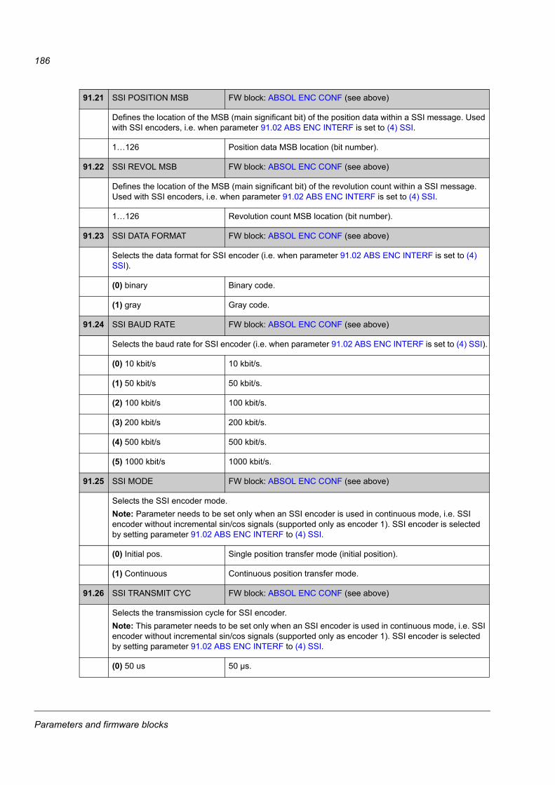
186
91.21 SSI POSITION MSB FW block: ABSOL ENC CONF (see above)
Defines the location of the MSB (main significant bit) of the position data within a SSI message. Used with SSI encoders, i.e. when parameter 91.02 ABS ENC INTERF is set to (4) SSI.
1…126 Position data MSB location (bit number).
91.22 SSI REVOL MSB FW block: ABSOL ENC CONF (see above)
Defines the location of the MSB (main significant bit) of the revolution count within a SSI message. Used with SSI encoders, i.e. when parameter 91.02 ABS ENC INTERF is set to (4) SSI.
1…126 Revolution count MSB location (bit number).
91.23 SSI DATA FORMAT FW block: ABSOL ENC CONF (see above)
Selects the data format for SSI encoder (i.e. when parameter 91.02 ABS ENC INTERF is set to (4) SSI).
(0) binary Binary code.
(1) gray Gray code.
91.24 SSI BAUD RATE FW block: ABSOL ENC CONF (see above)
Selects the baud rate for SSI encoder (i.e. when parameter 91.02 ABS ENC INTERF is set to (4) SSI).
(0) 10 kbit/s 10 kbit/s.
(1) 50 kbit/s 50 kbit/s.
(2) 100 kbit/s 100 kbit/s.
(3) 200 kbit/s 200 kbit/s.
(4) 500 kbit/s 500 kbit/s.
(5) 1000 kbit/s 1000 kbit/s.
91.25 SSI MODE FW block: ABSOL ENC CONF (see above)
Selects the SSI encoder mode.Note: Parameter needs to be set only when an SSI encoder is used in continuous mode, i.e. SSI encoder without incremental sin/cos signals (supported only as encoder 1). SSI encoder is selected by setting parameter 91.02 ABS ENC INTERF to (4) SSI.
(0) Initial pos. Single position transfer mode (initial position).
(1) Continuous Continuous position transfer mode.
91.26 SSI TRANSMIT CYC FW block: ABSOL ENC CONF (see above)
Selects the transmission cycle for SSI encoder.Note: This parameter needs to be set only when an SSI encoder is used in continuous mode, i.e. SSI encoder without incremental sin/cos signals (supported only as encoder 1). SSI encoder is selected by setting parameter 91.02 ABS ENC INTERF to (4) SSI.
(0) 50 us 50 µs.
Parameters and firmware blocks
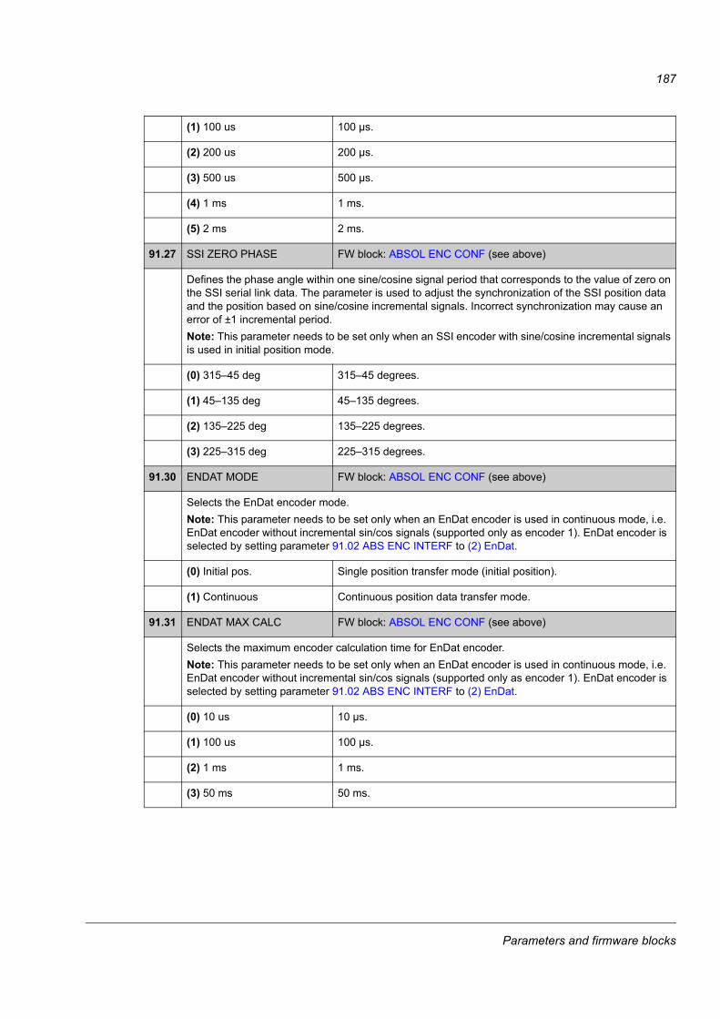
187
(1) 100 us 100 µs.
(2) 200 us 200 µs.
(3) 500 us 500 µs.
(4) 1 ms 1 ms.
(5) 2 ms 2 ms.
91.27 SSI ZERO PHASE FW block: ABSOL ENC CONF (see above)
Defines the phase angle within one sine/cosine signal period that corresponds to the value of zero on the SSI serial link data. The parameter is used to adjust the synchronization of the SSI position data and the position based on sine/cosine incremental signals. Incorrect synchronization may cause an error of ±1 incremental period.Note: This parameter needs to be set only when an SSI encoder with sine/cosine incremental signals is used in initial position mode.
(0) 315–45 deg 315–45 degrees.
(1) 45–135 deg 45–135 degrees.
(2) 135–225 deg 135–225 degrees.
(3) 225–315 deg 225–315 degrees.
91.30 ENDAT MODE FW block: ABSOL ENC CONF (see above)
Selects the EnDat encoder mode.Note: This parameter needs to be set only when an EnDat encoder is used in continuous mode, i.e. EnDat encoder without incremental sin/cos signals (supported only as encoder 1). EnDat encoder is selected by setting parameter 91.02 ABS ENC INTERF to (2) EnDat.
(0) Initial pos. Single position transfer mode (initial position).
(1) Continuous Continuous position data transfer mode.
91.31 ENDAT MAX CALC FW block: ABSOL ENC CONF (see above)
Selects the maximum encoder calculation time for EnDat encoder.Note: This parameter needs to be set only when an EnDat encoder is used in continuous mode, i.e. EnDat encoder without incremental sin/cos signals (supported only as encoder 1). EnDat encoder is selected by setting parameter 91.02 ABS ENC INTERF to (2) EnDat.
(0) 10 us 10 µs.
(1) 100 us 100 µs.
(2) 1 ms 1 ms.
(3) 50 ms 50 ms.
Parameters and firmware blocks

188
Group 92 RESOLVER CONFResolver configuration; used when parameter 90.01 ENCODER 1 SEL / 90.02 ENCODER 2 SEL is set to (5) FEN-21 RES.
The optional FEN-21 Resolver Interface module is compatible with resolvers which are excited by sinusoidal voltage (to the rotor winding) and which generate sine and cosine signals proportional to the rotor angle (to stator windings).
Note: Configuration data is written into the logic registers of the adapter once after the power-up. If parameter values are changed, save values into the permanent memory by parameter 16.07 PARAM SAVE. The new settings will take effect when the drive is powered up again, or after re-configuration is forced by parameter 90.10 ENC PAR REFRESH.
Resolver autotuning is performed automatically whenever the resolver input is activated after changes to parameters 92.02 EXC SIGNAL AMPL or 92.03 EXC SIGNAL FREQ. Autotuning must be forced after any changes in the resolver cable connection. This can be done by setting either 92.02 EXC SIGNAL AMPL or 92.03 EXC SIGNAL FREQ to its already existing value, and then setting parameter 90.10 ENC PAR REFRESH to 1.
If the resolver (or absolute encoder) is used for feedback from a permanent magnet motor, an AUTOPHASING ID run should be performed after replacement or any parameter changes. See parameter 99.13 IDRUN MODE and section Autophasing on page 38.
See also parameter group 90 on page 179, and FEN-21 Resolver Interface User’s Manual (3AFE68784859 [English]).
92Firmware block:RESOLVER CONF(92)
This block configures the resolver connection.
92.01 RESOLV POLEPAIRS FW block: RESOLVER CONF (see above)
Selects the number of pole pairs.
1…32 Number of pole pairs.
92.02 EXC SIGNAL AMPL FW block: RESOLVER CONF (see above)
Defines the amplitude of the excitation signal.
4.0…12.0 Vrms Excitation signal amplitude.
92.03 EXC SIGNAL FREQ FW block: RESOLVER CONF (see above)
Defines the frequency of the excitation signal.
1…20 kHz Excitation signal frequency.
RESOLVER CONF40
TLF11 10 msec (3)
92.01 RESOLV POLEPAIRS [ 1 ]
92.02 EXC SIGNAL AMPL [ 4.0 Vrms ]
92.03 EXC SIGNAL FREQ [ 1 kHz ]
Parameters and firmware blocks

189
Group 93 PULSE ENC CONFTTL/HTL input and TTL output configuration. See also parameter group 90 on page 179, and the appropriate encoder extension module manual.
Parameters 93.01…93.06 are used when a TTL/HTL encoder is used as encoder 1 (see parameter 90.01 ENCODER 1 SEL).
Parameters 93.11…93.16 are used when a TTL/HTL encoder is used as encoder 2 (see parameter 90.02 ENCODER 2 SEL).
Typically, only parameter 93.01/93.11 needs to be set for TTL/HTL encoders.
Note: Configuration data is written into the logic registers of the adapter once after the power-up. If parameter values are changed, save values into the permanent memory by parameter 16.07 PARAM SAVE. The new settings will take effect when the drive is powered up again, or after re-configuration is forced by parameter 90.10 ENC PAR REFRESH.
93Firmware block:PULSE ENC CONF(93)
This block configures the TTL/HTL input and TTL output.
93.01 ENC1 PULSE NR FW block: PULSE ENC CONF (see above)
Defines the pulse number per revolution for encoder 1.
0…65535 Pulses per revolution for encoder 1.
93.02 ENC1 TYPE FW block: PULSE ENC CONF (see above)
Selects the type of encoder 1.
(0) Quadrature Quadrature encoder (two channels, channels A and B).
(1) single track Single track encoder (one channel, channel A).
93.03 ENC1 SP CALCMODE FW block: PULSE ENC CONF (see above)
Selects the speed calculation mode for encoder 1.*When single track mode has been selected by parameter 93.02 ENC1 TYPE, the speed is always positive.
PULSE ENC CONF43
TLF11 10 msec (4)
93.01 ENC1 PULSE NR [ 0 ]
93.02 ENC1 TYPE [ Quadrature ]
93.03 ENC1 SP CALCMODE [ auto rising ]
93.04 ENC1 POS EST ENA [ TRUE ]
93.05 ENC1 SP EST ENA [ FALSE ]
93.06 ENC1 OSC LIM [ 4880Hz ]
93.11 ENC2 PULSE NR [ 0 ]
93.12 ENC2 TYPE [ Quadrature ]
93.13 ENC2 SP CALCMODE [ auto rising ]
93.14 ENC2 POS EST ENA [ TRUE ]
93.15 ENC2 SP EST ENA [ FALSE ]
93.16 ENC2 OSC LIM [ 4880Hz ]
Parameters and firmware blocks

190
(0) A&B all Channels A and B: Rising and falling edges are used for speed calculation. Channel B: Defines the direction of rotation. *Note: When single track mode has been selected by parameter 93.02 ENC1 TYPE, setting 0 acts like setting 1.
(1) A all Channel A: Rising and falling edges are used for speed calculation. Channel B: Defines the direction of rotation. *
(2) A rising Channel A: Rising edges are used for speed calculation. Channel B: Defines the direction of rotation. *
(3) A falling Channel A: Falling edges are used for speed calculation. Channel B: Defines the direction of rotation. *
(4) auto rising Used mode (0, 1, 2 or 3) is changed automatically depending on the pulse frequency according to the following table:
(5) auto falling
93.04 ENC1 POS EST ENA FW block: PULSE ENC CONF (see above)
Selects whether position estimation is used with encoder 1 to increase position data resolution or not.
(0) FALSE Measured position (Resolution: 4 x pulses per revolution for quadrature encoders, 2 x pulses per revolution for single track encoders.)
(1) TRUE Estimated position. (Uses position extrapolation. Extrapolated at the time of data request.)
93.05 ENC1 SP EST ENA FW block: PULSE ENC CONF (see above)
Selects whether calculated or estimated speed is used with encoder 1.
(0) FALSE Last calculated speed (calculation interval is 62.5 µs…4 ms).
(1) TRUE Estimated speed (estimated at the time of data request) Estimation increases the speed ripple in steady state operation, but improves the dynamics.
93.06 ENC1 OSC LIM FW block: PULSE ENC CONF (see above)
Activates transient filter for encoder 1. Changes of direction of rotation are ignored above the selected pulse frequency.
(0) 4880Hz Change in rotation of direction allowed below 4880 Hz.
(1) 2440Hz Change in rotation of direction allowed below 2440 Hz.
(2) 1220Hz Change in rotation of direction allowed below 1220 Hz.
(3) Disabled Change in rotation of direction allowed at any pulse frequency.
93.03 = 4 93.03 = 5Pulse frequency of the channel(s)
Used mode0 0 < 2442 Hz1 1 2442…4884 Hz2 3 > 4884 Hz
Parameters and firmware blocks

191
93.11 ENC2 PULSE NR FW block: PULSE ENC CONF (see above)
Defines the pulse number per revolution for encoder 2.
0…65535 Pulses per revolution for encoder 2.
93.12 ENC2 TYPE FW block: PULSE ENC CONF (see above)
Selects the type of encoder 2. For selections, see parameter 93.02 ENC1 TYPE.
93.13 ENC2 SP CALCMODE FW block: PULSE ENC CONF (see above)
Selects the speed calculation mode for encoder 2.For selections, see parameter 93.03 ENC1 SP CALCMODE.
93.14 ENC2 POS EST ENA FW block: PULSE ENC CONF (see above)
Selects whether measured or estimated position is used with encoder 2.For selections, see parameter 93.04 ENC1 POS EST ENA.
93.15 ENC2 SP EST ENA FW block: PULSE ENC CONF (see above)
Selects whether calculated or estimated speed is used with encoder 2.For selections, see parameter 93.05 ENC1 SP EST ENA.
93.16 ENC2 OSC LIM FW block: PULSE ENC CONF (see above)
Activates transient filter for encoder 2. Changes of direction of rotation are ignored above the selected pulse frequency.For selections, see parameter 93.06 ENC1 OSC LIM.
93.21 EMUL PULSE NR FW block: ENCODER (page 179)
Defines the number of TTL pulses per revolution used in encoder emulation.Encoder emulation is enabled by parameter 90.03 EMUL MODE SEL.
0…65535 TTL pulses used in encoder emulation.
93.22 EMUL POS REF FW block: ENCODER (page 179)
Selects the source for the position value used in encoder emulation when parameter 90.03 EMUL MODE SEL is set to (1) FEN-01 SWref, (4) FEN-11 SWref, (7) FEN-21 SWref or (10) FEN-31 SWref. See parameter group 90.The source can be any actual or reference position value (except 1.09 ENCODER 1 POS and 1.11 ENCODER 2 POS).
Value pointer: Group and index
93.23 EMUL POS OFFSET FW block: None
Defines the zero point for emulated position in relation of the zero point of the input position (within one revolution). The input position is selected by parameter 90.03 EMUL MODE SEL.For example, if the offset is 0, an emulated zero pulse is generated each time the input position moves across 0. With an offset of 0.5, an emulated zero pulse is generated each time the input position (within one revolution) moves across 0.5.
0 … 0.99998 rev Emulated zero pulse position offset.
Parameters and firmware blocks
192
Group 95 HW CONFIGURATIONMiscellaneous hardware-related settings.
9595.01 CTRL UNIT SUPPLY FW block: None
Defines the manner in which the drive control unit is powered.
(0) Internal 24V The drive control unit is powered from the drive power unit it is mounted on.
(1) External 24V The drive control unit is powered from an external power supply.
95.02 EXTERNAL CHOKE FW block: None
Defines if the drive is equipped with an AC choke or not.
(0) NO The drive is not equipped with an AC choke.
(1) YES The drive is equipped with an AC choke.
Parameters and firmware blocks
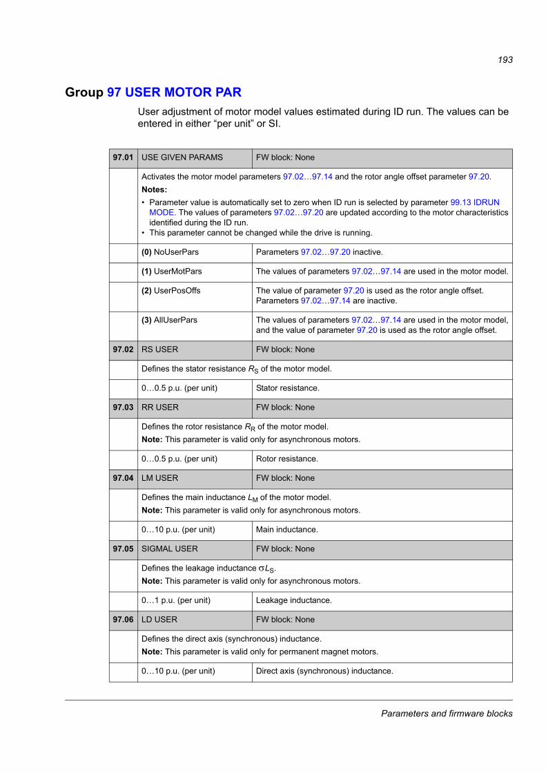
193
Group 97 USER MOTOR PARUser adjustment of motor model values estimated during ID run. The values can be entered in either “per unit” or SI.
9797.01 USE GIVEN PARAMS FW block: None
Activates the motor model parameters 97.02…97.14 and the rotor angle offset parameter 97.20.Notes:• Parameter value is automatically set to zero when ID run is selected by parameter 99.13 IDRUN
MODE. The values of parameters 97.02…97.20 are updated according to the motor characteristics identified during the ID run.
• This parameter cannot be changed while the drive is running.
(0) NoUserPars Parameters 97.02…97.20 inactive.
(1) UserMotPars The values of parameters 97.02…97.14 are used in the motor model.
(2) UserPosOffs The value of parameter 97.20 is used as the rotor angle offset. Parameters 97.02…97.14 are inactive.
(3) AllUserPars The values of parameters 97.02…97.14 are used in the motor model, and the value of parameter 97.20 is used as the rotor angle offset.
97.02 RS USER FW block: None
Defines the stator resistance RS of the motor model.
0…0.5 p.u. (per unit) Stator resistance.
97.03 RR USER FW block: None
Defines the rotor resistance RR of the motor model. Note: This parameter is valid only for asynchronous motors.
0…0.5 p.u. (per unit) Rotor resistance.
97.04 LM USER FW block: None
Defines the main inductance LM of the motor model.Note: This parameter is valid only for asynchronous motors.
0…10 p.u. (per unit) Main inductance.
97.05 SIGMAL USER FW block: None
Defines the leakage inductance σLS.Note: This parameter is valid only for asynchronous motors.
0…1 p.u. (per unit) Leakage inductance.
97.06 LD USER FW block: None
Defines the direct axis (synchronous) inductance. Note: This parameter is valid only for permanent magnet motors.
0…10 p.u. (per unit) Direct axis (synchronous) inductance.
Parameters and firmware blocks
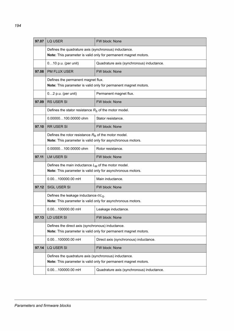
194
97.07 LQ USER FW block: None
Defines the quadrature axis (synchronous) inductance. Note: This parameter is valid only for permanent magnet motors.
0…10 p.u. (per unit) Quadrature axis (synchronous) inductance.
97.08 PM FLUX USER FW block: None
Defines the permanent magnet flux. Note: This parameter is valid only for permanent magnet motors.
0…2 p.u. (per unit) Permanent magnet flux.
97.09 RS USER SI FW block: None
Defines the stator resistance RS of the motor model.
0.00000…100.00000 ohm Stator resistance.
97.10 RR USER SI FW block: None
Defines the rotor resistance RR of the motor model. Note: This parameter is valid only for asynchronous motors.
0.00000…100.00000 ohm Rotor resistance.
97.11 LM USER SI FW block: None
Defines the main inductance LM of the motor model.Note: This parameter is valid only for asynchronous motors.
0.00…100000.00 mH Main inductance.
97.12 SIGL USER SI FW block: None
Defines the leakage inductance σLS.Note: This parameter is valid only for asynchronous motors.
0.00…100000.00 mH Leakage inductance.
97.13 LD USER SI FW block: None
Defines the direct axis (synchronous) inductance. Note: This parameter is valid only for permanent magnet motors.
0.00…100000.00 mH Direct axis (synchronous) inductance.
97.14 LQ USER SI FW block: None
Defines the quadrature axis (synchronous) inductance. Note: This parameter is valid only for permanent magnet motors.
0.00…100000.00 mH Quadrature axis (synchronous) inductance.
Parameters and firmware blocks
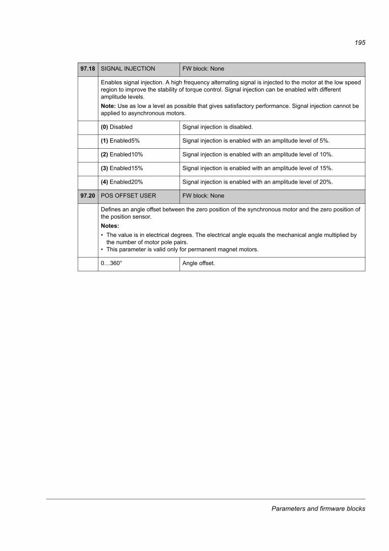
195
97.18 SIGNAL INJECTION FW block: None
Enables signal injection. A high frequency alternating signal is injected to the motor at the low speed region to improve the stability of torque control. Signal injection can be enabled with different amplitude levels.Note: Use as low a level as possible that gives satisfactory performance. Signal injection cannot be applied to asynchronous motors.
(0) Disabled Signal injection is disabled.
(1) Enabled5% Signal injection is enabled with an amplitude level of 5%.
(2) Enabled10% Signal injection is enabled with an amplitude level of 10%.
(3) Enabled15% Signal injection is enabled with an amplitude level of 15%.
(4) Enabled20% Signal injection is enabled with an amplitude level of 20%.
97.20 POS OFFSET USER FW block: None
Defines an angle offset between the zero position of the synchronous motor and the zero position of the position sensor.Notes:• The value is in electrical degrees. The electrical angle equals the mechanical angle multiplied by
the number of motor pole pairs.• This parameter is valid only for permanent magnet motors.
0…360° Angle offset.
Parameters and firmware blocks
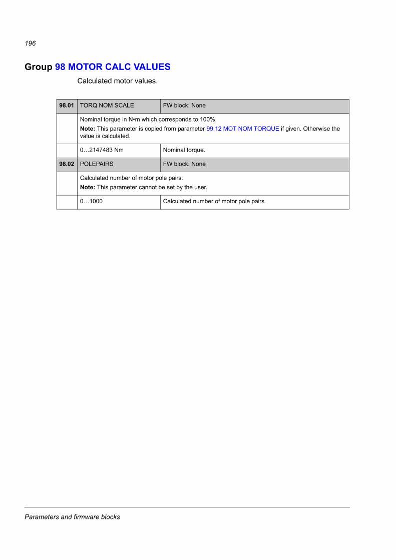
196
Group 98 MOTOR CALC VALUESCalculated motor values.
9898.01 TORQ NOM SCALE FW block: None
Nominal torque in N•m which corresponds to 100%.Note: This parameter is copied from parameter 99.12 MOT NOM TORQUE if given. Otherwise the value is calculated.
0…2147483 Nm Nominal torque.
98.02 POLEPAIRS FW block: None
Calculated number of motor pole pairs.Note: This parameter cannot be set by the user.
0…1000 Calculated number of motor pole pairs.
Parameters and firmware blocks
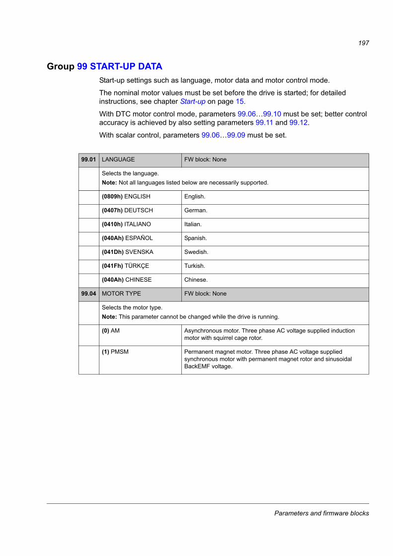
197
Group 99 START-UP DATAStart-up settings such as language, motor data and motor control mode.
The nominal motor values must be set before the drive is started; for detailed instructions, see chapter Start-up on page 15.
With DTC motor control mode, parameters 99.06…99.10 must be set; better control accuracy is achieved by also setting parameters 99.11 and 99.12.
With scalar control, parameters 99.06…99.09 must be set.
9999.01 LANGUAGE FW block: None
Selects the language.Note: Not all languages listed below are necessarily supported.
(0809h) ENGLISH English.
(0407h) DEUTSCH German.
(0410h) ITALIANO Italian.
(040Ah) ESPAÑOL Spanish.
(041Dh) SVENSKA Swedish.
(041Fh) TÜRKÇE Turkish.
(040Ah) CHINESE Chinese.
99.04 MOTOR TYPE FW block: None
Selects the motor type.Note: This parameter cannot be changed while the drive is running.
(0) AM Asynchronous motor. Three phase AC voltage supplied induction motor with squirrel cage rotor.
(1) PMSM Permanent magnet motor. Three phase AC voltage supplied synchronous motor with permanent magnet rotor and sinusoidal BackEMF voltage.
Parameters and firmware blocks
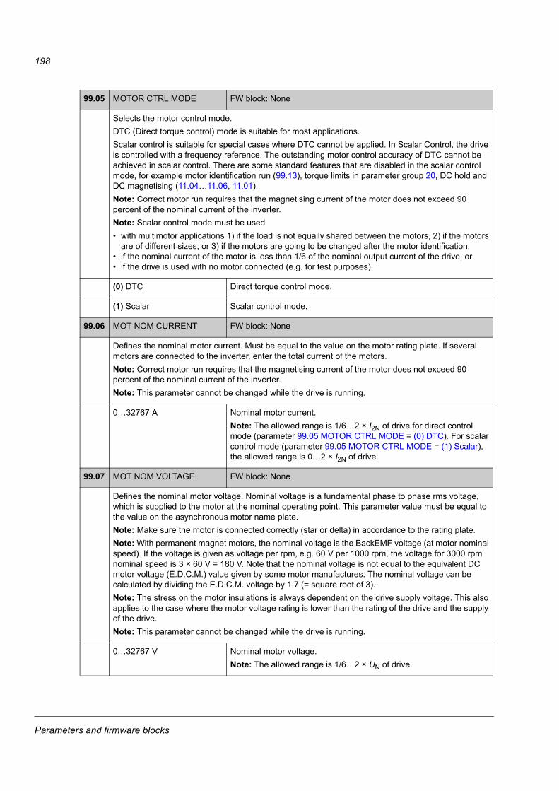
198
99.05 MOTOR CTRL MODE FW block: None
Selects the motor control mode.DTC (Direct torque control) mode is suitable for most applications.Scalar control is suitable for special cases where DTC cannot be applied. In Scalar Control, the drive is controlled with a frequency reference. The outstanding motor control accuracy of DTC cannot be achieved in scalar control. There are some standard features that are disabled in the scalar control mode, for example motor identification run (99.13), torque limits in parameter group 20, DC hold and DC magnetising (11.04…11.06, 11.01).Note: Correct motor run requires that the magnetising current of the motor does not exceed 90 percent of the nominal current of the inverter.Note: Scalar control mode must be used• with multimotor applications 1) if the load is not equally shared between the motors, 2) if the motors
are of different sizes, or 3) if the motors are going to be changed after the motor identification,• if the nominal current of the motor is less than 1/6 of the nominal output current of the drive, or• if the drive is used with no motor connected (e.g. for test purposes).
(0) DTC Direct torque control mode.
(1) Scalar Scalar control mode.
99.06 MOT NOM CURRENT FW block: None
Defines the nominal motor current. Must be equal to the value on the motor rating plate. If several motors are connected to the inverter, enter the total current of the motors.Note: Correct motor run requires that the magnetising current of the motor does not exceed 90 percent of the nominal current of the inverter.Note: This parameter cannot be changed while the drive is running.
0…32767 A Nominal motor current.Note: The allowed range is 1/6…2 × I2N of drive for direct control mode (parameter 99.05 MOTOR CTRL MODE = (0) DTC). For scalar control mode (parameter 99.05 MOTOR CTRL MODE = (1) Scalar), the allowed range is 0…2 × I2N of drive.
99.07 MOT NOM VOLTAGE FW block: None
Defines the nominal motor voltage. Nominal voltage is a fundamental phase to phase rms voltage, which is supplied to the motor at the nominal operating point. This parameter value must be equal to the value on the asynchronous motor name plate.Note: Make sure the motor is connected correctly (star or delta) in accordance to the rating plate.Note: With permanent magnet motors, the nominal voltage is the BackEMF voltage (at motor nominal speed). If the voltage is given as voltage per rpm, e.g. 60 V per 1000 rpm, the voltage for 3000 rpm nominal speed is 3 × 60 V = 180 V. Note that the nominal voltage is not equal to the equivalent DC motor voltage (E.D.C.M.) value given by some motor manufactures. The nominal voltage can be calculated by dividing the E.D.C.M. voltage by 1.7 (= square root of 3).Note: The stress on the motor insulations is always dependent on the drive supply voltage. This also applies to the case where the motor voltage rating is lower than the rating of the drive and the supply of the drive.Note: This parameter cannot be changed while the drive is running.
0…32767 V Nominal motor voltage.Note: The allowed range is 1/6…2 × UN of drive.
Parameters and firmware blocks
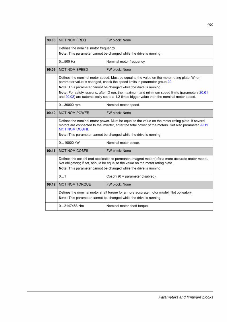
199
99.08 MOT NOM FREQ FW block: None
Defines the nominal motor frequency.Note: This parameter cannot be changed while the drive is running.
5…500 Hz Nominal motor frequency.
99.09 MOT NOM SPEED FW block: None
Defines the nominal motor speed. Must be equal to the value on the motor rating plate. When parameter value is changed, check the speed limits in parameter group 20.Note: This parameter cannot be changed while the drive is running.Note: For safety reasons, after ID run, the maximum and minimum speed limits (parameters 20.01 and 20.02) are automatically set to a 1.2 times bigger value than the nominal motor speed.
0…30000 rpm Nominal motor speed.
99.10 MOT NOM POWER FW block: None
Defines the nominal motor power. Must be equal to the value on the motor rating plate. If several motors are connected to the inverter, enter the total power of the motors. Set also parameter 99.11 MOT NOM COSFII.Note: This parameter cannot be changed while the drive is running.
0…10000 kW Nominal motor power.
99.11 MOT NOM COSFII FW block: None
Defines the cosphi (not applicable to permanent magnet motors) for a more accurate motor model. Not obligatory; if set, should be equal to the value on the motor rating plate.Note: This parameter cannot be changed while the drive is running.
0…1 Cosphi (0 = parameter disabled).
99.12 MOT NOM TORQUE FW block: None
Defines the nominal motor shaft torque for a more accurate motor model. Not obligatory.Note: This parameter cannot be changed while the drive is running.
0…2147483 Nm Nominal motor shaft torque.
Parameters and firmware blocks
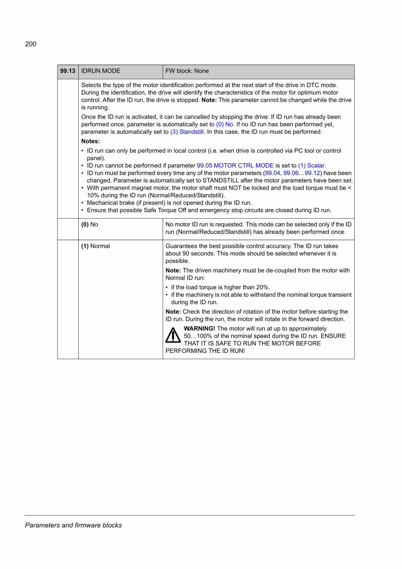
200
99.13 IDRUN MODE FW block: None
Selects the type of the motor identification performed at the next start of the drive in DTC mode. During the identification, the drive will identify the characteristics of the motor for optimum motor control. After the ID run, the drive is stopped. Note: This parameter cannot be changed while the drive is running.Once the ID run is activated, it can be cancelled by stopping the drive: If ID run has already been performed once, parameter is automatically set to (0) No. If no ID run has been performed yet, parameter is automatically set to (3) Standstill. In this case, the ID run must be performed.Notes:• ID run can only be performed in local control (i.e. when drive is controlled via PC tool or control
panel).• ID run cannot be performed if parameter 99.05 MOTOR CTRL MODE is set to (1) Scalar.• ID run must be performed every time any of the motor parameters (99.04, 99.06…99.12) have been
changed. Parameter is automatically set to STANDSTILL after the motor parameters have been set.• With permanent magnet motor, the motor shaft must NOT be locked and the load torque must be <
10% during the ID run (Normal/Reduced/Standstill).• Mechanical brake (if present) is not opened during the ID run.• Ensure that possible Safe Torque Off and emergency stop circuits are closed during ID run.
(0) No No motor ID run is requested. This mode can be selected only if the ID run (Normal/Reduced/Standstill) has already been performed once.
(1) Normal Guarantees the best possible control accuracy. The ID run takes about 90 seconds. This mode should be selected whenever it is possible.Note: The driven machinery must be de-coupled from the motor with Normal ID run:• if the load torque is higher than 20%.• if the machinery is not able to withstand the nominal torque transient
during the ID run.Note: Check the direction of rotation of the motor before starting the ID run. During the run, the motor will rotate in the forward direction.
WARNING! The motor will run at up to approximately 50…100% of the nominal speed during the ID run. ENSURE THAT IT IS SAFE TO RUN THE MOTOR BEFORE
PERFORMING THE ID RUN!
Parameters and firmware blocks
201
(2) Reduced Reduced ID Run. This mode should be selected instead of the Normal ID Run• if mechanical losses are higher than 20% (i.e. the motor cannot be
de-coupled from the driven equipment), or• if flux reduction is not allowed while the motor is running (i.e. in case
of a motor with an integrated brake supplied from the motor terminals), or
• if large speed vibrations are detected during the Normal ID Run.With Reduced ID run, the control in the field weakening area or at high torques is not necessarily as accurate as with the Normal ID run. Reduced ID run is completed faster than the Normal ID Run (< 90 seconds).Note: Check the direction of rotation of the motor before starting the ID run. During the run, the motor will rotate in the forward direction.
WARNING! The motor will run at up to approximately 50…100% of the nominal speed during the ID run. ENSURE THAT IT IS SAFE TO RUN THE MOTOR BEFORE
PERFORMING THE ID RUN!
(3) Standstill Standstill ID run. The motor is injected with DC current. With asynchronous motor, the motor shaft is not rotating (with permanent magnet motor the shaft can rotate < 0.5 revolution).Note: This mode should be selected only if the Normal or Reduced ID run is not possible due to the restrictions caused by the connected mechanics (e.g. with lift or crane applications).
(4) Autophasing During autophasing, the start angle of the motor is determined. Note that other motor model values are not updated. See also parameter 11.07 AUTOPHASING MODE, and section Autophasing on page 38.Notes:• Autophasing can only be selected after the Normal/Reduced/
Standstill ID run has been performed once. Autophasing is used when an absolute encoder, a resolver or an encoder with commutation signals has been added/changed to a permanent magnet motor and there is no need to perform the Normal/Reduced/Standstill ID run again.
• During Autophasing the motor shaft must NOT be locked and the load torque must be < 5%.
(5) Cur meas cal Current offset and gain measurement calibration. The calibration will be performed at next start.
Parameters and firmware blocks
202
(6) Advanced Advanced ID run. Guarantees the best possible control accuracy. The ID run can take a couple of minutes. This mode should be selected when top performance is needed in the whole operating area.Notes:• The driven machinery must be de-coupled from the motor because
of high torque and speed transients that are applied.• During the run, the motor may rotate both in the forward and reverse
direction.WARNING! The motor may run at up to the maximum (positive) and minimum (negative) allowed speed during the ID run. Several accelerations and decelerations are done. The
maximum torque, current and speed allowed by the limit parameters may be utilized. ENSURE THAT IT IS SAFE TO RUN THE MOTOR BEFORE PERFORMING THE ID RUN!
Parameters and firmware blocks

203
Parameter data
What this chapter containsThis chapter lists the parameters of the drive with some additional data. For the parameter descriptions, see chapter Parameters and firmware blocks.
TermsTerm Definition
Actual signal Signal measured or calculated by the drive. Can be monitored by the user. No user setting is possible.
Def Default value
enum Enumerated list, i.e. selection list
FbEq Fieldbus equivalent: The scaling between the value shown on the panel and the integer used in serial communication.
Page no. Page number for more information
INT32 32-bit integer value (31 bits + sign)
Bit pointer Bit pointer. A bit pointer points to a single bit in the value of another parameter.
Val pointer Value pointer. A value pointer points to the value of another parameter.
Parameter An operation instruction of the drive that is often user-adjustable. Parameters that are signals measured or calculated by the drive are called actual signals.
Pb Packed boolean
PT Parameter protection type. See WP, WPD and WP0.
REAL
REAL24
Save PF Parameter setting is protected against power failure.
Type Data type. See enum, INT32, Bit pointer, Val pointer, Pb, REAL, REAL24, UINT32.
UINT32 32-bit unsigned integer value
WP Write protected parameter (i.e. read only)
WPD Write protected parameter while drive is running
WP0 Parameter can only be set to zero.
16-bit value 16-bit value (31 bits + sign)
= integer value = fractional value
8-bit value 24-bit value (31 bits + sign)
= integer value = fractional value
Parameter data
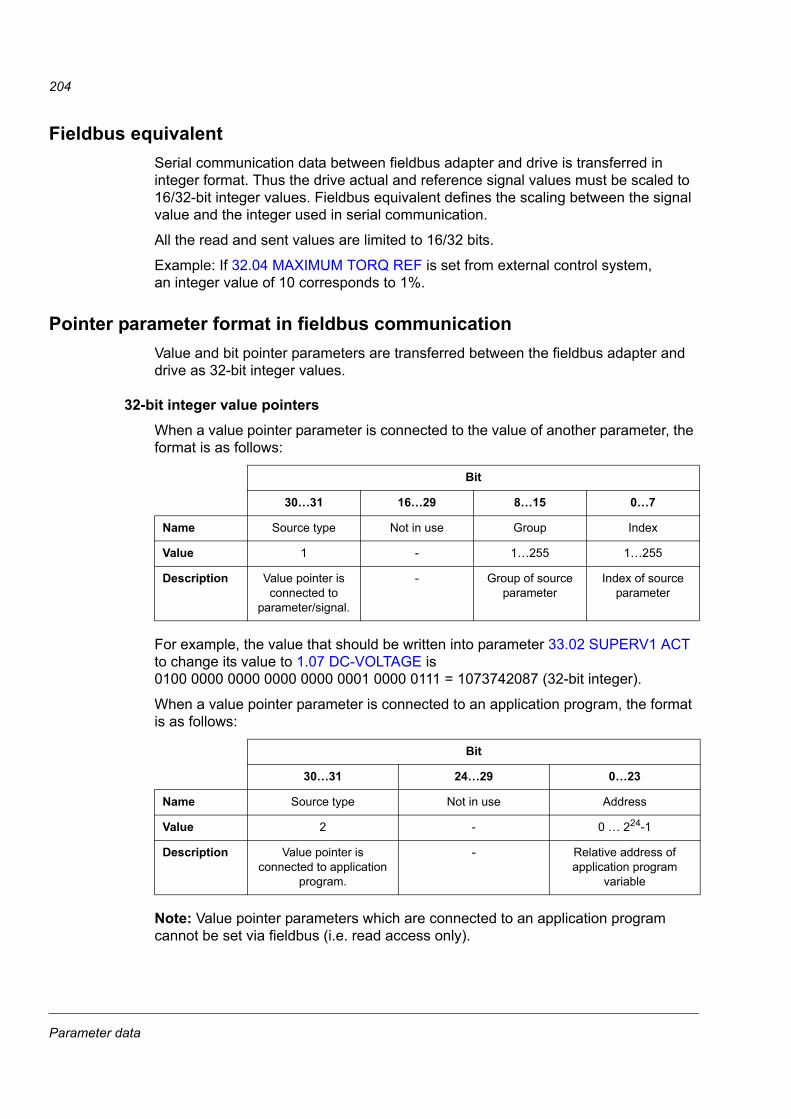
204
Fieldbus equivalentSerial communication data between fieldbus adapter and drive is transferred in integer format. Thus the drive actual and reference signal values must be scaled to 16/32-bit integer values. Fieldbus equivalent defines the scaling between the signal value and the integer used in serial communication.
All the read and sent values are limited to 16/32 bits.
Example: If 32.04 MAXIMUM TORQ REF is set from external control system, an integer value of 10 corresponds to 1%.
Pointer parameter format in fieldbus communicationValue and bit pointer parameters are transferred between the fieldbus adapter and drive as 32-bit integer values.
32-bit integer value pointersWhen a value pointer parameter is connected to the value of another parameter, the format is as follows:
For example, the value that should be written into parameter 33.02 SUPERV1 ACT to change its value to 1.07 DC-VOLTAGE is 0100 0000 0000 0000 0000 0001 0000 0111 = 1073742087 (32-bit integer).
When a value pointer parameter is connected to an application program, the format is as follows:
Note: Value pointer parameters which are connected to an application program cannot be set via fieldbus (i.e. read access only).
Bit
30…31 16…29 8…15 0…7
Name Source type Not in use Group Index
Value 1 - 1…255 1…255
Description Value pointer is connected to
parameter/signal.
- Group of source parameter
Index of source parameter
Bit
30…31 24…29 0…23
Name Source type Not in use Address
Value 2 - 0 … 224-1
Description Value pointer is connected to application
program.
- Relative address of application program
variable
Parameter data
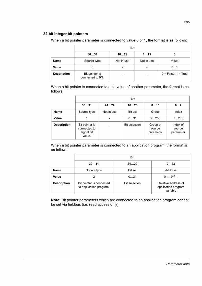
205
32-bit integer bit pointersWhen a bit pointer parameter is connected to value 0 or 1, the format is as follows:
When a bit pointer is connected to a bit value of another parameter, the format is as follows:
When a bit pointer parameter is connected to an application program, the format is as follows:
Note: Bit pointer parameters which are connected to an application program cannot be set via fieldbus (i.e. read access only).
Bit
30…31 16…29 1…15 0
Name Source type Not in use Not in use Value
Value 0 - - 0…1
Description Bit pointer is connected to 0/1.
- - 0 = False, 1 = True
Bit
30…31 24…29 16…23 8…15 0…7
Name Source type Not in use Bit sel Group Index
Value 1 - 0…31 2…255 1…255
Description Bit pointer is connected to
signal bit value.
- Bit selection Group of source
parameter
Index of source
parameter
Bit
30…31 24…29 0…23
Name Source type Bit sel Address
Value 2 0…31 0 … 224-1
Description Bit pointer is connected to application program.
Bit selection Relative address of application program
variable
Parameter data
206
01111111111111111111111111110222222222222
Actual signals (Parameter groups 1…9)Index Name Type Range Unit FbEq Update
timeData
lengthPT Save
PFPage no.
1 ACTUAL VALUES.01 SPEED ACT REAL -30000…30000 rpm 1 = 100 250 µs 32 WP 63.02 SPEED ACT PERC REAL -1000…1000 % 1 = 100 2 ms 32 WP 63.03 FREQUENCY REAL -30000…30000 Hz 1 = 100 2 ms 32 WP 63.04 CURRENT REAL 0…30000 A 1 = 100 10 ms 32 WP 63.05 CURRENT PERC REAL 0…1000 % 1 = 10 2 ms 16 WP 63.06 TORQUE REAL -1600…1600 % 1 = 10 2 ms 16 WP 63.07 DC-VOLTAGE REAL - V 1 = 100 2 ms 32 WP 63.08 ENCODER 1 SPEED REAL - rpm 1 = 100 250 µs 32 WP 63.09 ENCODER 1 POS REAL24 - rev 1=100000000 250 µs 32 WP 63.10 ENCODER 2 SPEED REAL - rpm 1 = 100 250 µs 32 WP 64.11 ENCODER 2 POS REAL24 - rev 1=100000000 250 µs 32 WP 64.12 POS ACT REAL -32768…32767 rev 1 = 1000 250 µs 32 WP 64.13 POS 2ND ENC REAL -32768…32767 revs 1 = 1 250 µs 32 WP 64.14 SPEED ESTIMATED REAL -30000…30000 rpm 1 = 100 2 ms 32 WP 64.15 TEMP INVERTER REAL24 -40…160 °C 1 = 10 2 ms 16 WP 64.16 TEMP BC REAL24 -40…160 °C 1 = 10 2 ms 16 WP 64.17 MOTOR TEMP REAL -10…250 °C 1 = 10 10 ms 16 WP 64.18 MOTOR TEMP EST INT32 -60…1000 °C 1 = 1 10 ms 16 WP x 64.19 USED SUPPLY VOLT REAL 0…1000 V 1 = 10 10 ms 16 WP 64.20 BRAKE RES LOAD REAL24 0…1000 % 1 = 1 50 ms 16 WP 64.21 CPU USAGE UINT32 0…100 % 1 = 1 100 ms 16 WP 64.22 INVERTER POWER REAL -231…231 - 1 kW 1 = 100 10 ms 32 WP 65.26 ON TIME COUNTER INT32 0…35791394.1 h 1 = 100 10 ms 32 WP0 x 65.27 RUN TIME COUNTER INT32 0…35791394.1 h 1 = 100 10 ms 32 WP0 x 65.28 FAN ON-TIME INT32 0…35791394.1 h 1 = 100 10 ms 32 WP0 x 65.31 MECH TIME CONST REAL 0…32767 s 1 = 1000 10 ms 32 WP x 65.38 TEMP INT BOARD REAL24 -40…160 °C 1 = 10 2 ms 16 WP 652 I/O VALUES.01 DI STATUS Pb 0…0x3F - 1 = 1 2 ms 16 WP 66.02 RO STATUS Pb - - 1 = 1 2 ms 16 WP 66.03 DIO STATUS Pb - - 1 = 1 2 ms 16 WP 66.04 AI1 REAL - V or mA 1 = 1000 2 ms 16 WP 66.05 AI1 SCALED REAL - - 1 = 1000 250 µs 32 WP 66.06 AI2 REAL - V or mA 1 = 1000 2 ms 16 WP 66.07 AI2 SCALED REAL - - 1 = 1000 250 µs 32 WP 66.08 AO1 REAL - mA 1 = 1000 2 ms 16 WP 66.09 AO2 REAL - V 1 = 1000 2 ms 16 WP 66.10 DIO2 FREQ IN REAL -32768…32768 - 1 = 1000 2 ms 32 WP 66.11 DIO3 FREQ OUT REAL -32768…32768 Hz 1 = 1000 2 ms 32 WP 66.12 FBA MAIN CW Pb 0 …
0xFFFFFFFF- 1 = 1 500 µs 32 WP 67
Parameter data
207
2
222222203333333333333333333066666660888888
.13 FBA MAIN SW Pb 0 … 0xFFFFFFFF
- 1 = 1 500 µs 32 WP 69
.14 FBA MAIN REF1 INT32 -231…231 - 1 - 1 = 1 500 µs 32 WP 70
.15 FBA MAIN REF2 INT32 -231…231 - 1 - 1 = 1 500 µs 32 WP 70
.16 FEN DI STATUS Pb 0…0x33 - 1 = 1 500 µs 16 WP 70
.17 D2D MAIN CW Pb 0…0xFFFF - 1 = 1 500 µs 16 WP 70
.18 D2D FOLLOWER CW Pb 0…0xFFFF - 1 = 1 2 ms 16 WP 71
.19 D2D REF1 REAL -231…231 - 1 - 1 = 1 500 µs 32 WP 71
.20 D2D REF2 REAL -231…231 - 1 - 1 = 1 2 ms 32 WP 713 CONTROL VALUES.01 SPEED REF1 REAL -30000…30000 rpm 1 = 100 500 µs 32 WP 72.02 SPEED REF2 REAL -30000…30000 rpm 1 = 100 500 µs 32 WP 72.03 SPEEDREF RAMP IN REAL -30000…30000 rpm 1 = 100 500 µs 32 WP 72.04 SPEEDREF RAMPED REAL -30000…30000 rpm 1 = 100 500 µs 32 WP 72.05 SPEEDREF USED REAL -30000…30000 rpm 1 = 100 250 µs 32 WP 72.06 SPEED ERROR FILT REAL -30000…30000 rpm 1 = 100 250 µs 32 WP 72.07 ACC COMP TORQ REAL -1600…1600 % 1 = 10 250 µs 16 WP 72.08 TORQ REF SP CTRL REAL -1600…1600 % 1 = 10 250 µs 16 WP 72.09 TORQ REF1 REAL -1000…1000 % 1 = 10 500 µs 16 WP 72.10 TORQ REF RAMPED REAL -1000…1000 % 1 = 10 500 µs 16 WP 72.11 TORQ REF RUSHLIM REAL -1000…1000 % 1 = 10 250 µs 16 WP 72.12 TORQUE REF ADD REAL -1000…1000 % 1 = 10 250 µs 16 WP 72.13 TORQ REF TO TC REAL -1600…1600 % 1 = 10 250 µs 16 WP 72.14 BRAKE TORQ MEM REAL -1000…1000 % 1 = 10 2 ms 16 WP x 72.15 BRAKE COMMAND enum 0…1 - 1 = 1 2 ms 16 WP 73.16 FLUX REF USED REAL24 0…200 % 1 = 1 2 ms 16 WP 73.17 TORQUE REF USED REAL -1600…1600 % 1 = 10 250 µs 32 WP 73.20 MAX SPEED REF REAL 0…30000 rpm 1 = 100 2 ms 16 WP 73.21 MIN SPEED REF REAL -30000…0 rpm 1 = 100 2 ms 16 WP 736 DRIVE STATUS.01 STATUS WORD 1 Pb 0…65535 - 1 = 1 2 ms 16 WP 74.02 STATUS WORD 2 Pb 0…65535 - 1 = 1 2 ms 16 WP 75.03 SPEED CTRL STAT Pb 0…31 - 1 = 1 250 µs 16 WP 76.05 LIMIT WORD 1 Pb 0…255 - 1 = 1 250 µs 16 WP 76.07 TORQ LIM STATUS Pb 0…65535 - 1 = 1 250 µs 16 WP 77.12 OP MODE ACK enum 0…11 - 1 = 1 2 ms 16 WP 77.14 SUPERV STATUS Pb 0…65535 - 1 = 1 2 ms 16 WP 778 ALARMS & FAULTS.01 ACTIVE FAULT enum 0…65535 - 1 = 1 - 16 WP 78.02 LAST FAULT enum 0…65535 - 1 = 1 - 16 WP 78.03 FAULT TIME HI INT32 -231…231 - 1 days 1 = 1 - 32 WP 78.04 FAULT TIME LO INT32 -231…231 - 1 time 1 = 1 - 32 WP 78.05 ALARM LOGGER 1 UINT32 - - 1 = 1 2 ms 16 WP0 78.06 ALARM LOGGER 2 UINT32 - - 1 = 1 2 ms 16 WP0 79
Index Name Type Range Unit FbEq Update time
Data length
PT Save PF
Page no.
Parameter data
208
888888880999999999
1111111111111111111111
Parameter groups 10…99
.07 ALARM LOGGER 3 UINT32 - - 1 = 1 2 ms 16 WP0 79
.08 ALARM LOGGER 4 UINT32 - - 1 = 1 2 ms 16 WP0 80
.09 ALARM LOGGER 5 UINT32 - - 1 = 1 2 ms 16 WP0 80
.10 ALARM LOGGER 6 UINT32 - - 1 = 1 2 ms 16 WP0 80
.15 ALARM WORD 1 UINT32 - - 1 = 1 2 ms 16 WP0 81
.16 ALARM WORD 2 UINT32 - - 1 = 1 2 ms 16 WP0 81
.17 ALARM WORD 3 UINT32 - - 1 = 1 2 ms 16 WP0 82
.18 ALARM WORD 4 UINT32 - - 1 = 1 2 ms 16 WP0 829 SYSTEM INFO.01 DRIVE TYPE INT32 0…65535 - 1 = 1 - 16 WP 83.02 DRIVE RATING ID INT32 0…65535 - 1 = 1 - 16 WP 83.03 FIRMWARE ID Pb - - 1 = 1 - 16 WP 83.04 FIRMWARE VER Pb - - 1 = 1 - 16 WP 83.05 FIRMWARE PATCH Pb - - 1 = 1 - 16 WP 83.10 INT LOGIC VER Pb - - 1 = 1 - 32 WP 83.20 OPTION SLOT 1 INT32 0…18 - 1 = 1 - 16 WP 83.21 OPTION SLOT 2 INT32 0…18 - 1 = 1 - 16 WP 83.22 OPTION SLOT 3 INT32 0…18 - 1 = 1 - 16 WP 83
Index Parameter Type Range Unit FbEq Update time
Data len.
Def PT Save PF
Page no.
0 START/STOP0.01 EXT1 START FUNC enum 0…6 - - 2 ms 16 1 WPD 850.02 EXT1 START IN1 Bit pointer - 2 ms 32 P.02.01.00 WPD 850.03 EXT1 START IN2 Bit pointer - 2 ms 32 C.False WPD 860.04 EXT2 START FUNC enum 0…6 - - 2 ms 16 1 WPD 860.05 EXT2 START IN1 Bit pointer - 2 ms 32 P.02.01.00 WPD 870.06 EXT2 START IN2 Bit pointer - 2 ms 32 C.False WPD 870.07 JOG1 START Bit pointer - 2 ms 32 C.False WPD 870.08 FAULT RESET SEL Bit pointer - 2 ms 32 P.02.01.02 870.09 RUN ENABLE Bit pointer - 2 ms 32 C.True WPD 870.10 EM STOP OFF3 Bit pointer - 2 ms 32 C.True WPD 870.11 EM STOP OFF1 Bit pointer - 2 ms 32 C.True WPD 880.12 START INHIBIT enum 0…1 - 1 = 1 2 ms 16 0 880.13 FB CW USED Val pointer - 2 ms 32 P.02.12 WPD 880.14 JOG2 START Bit pointer - 2 ms 32 C.False WPD 880.15 JOG ENABLE Bit pointer - 2 ms 32 C.False WPD 880.16 D2D CW USED Val pointer - 2 ms 32 P.02.17 WPD 880.17 START ENABLE Bit pointer - 2 ms 32 C.True WPD 891 START/STOP MODE1.01 START MODE enum 0…2 - 1 = 1 - 16 1 WPD 901.02 DC MAGN TIME UINT32 0…10000 ms 1 = 1 - 16 500 WPD 911.03 STOP MODE enum 1…2 - 1 = 1 2 ms 16 2 91
Index Name Type Range Unit FbEq Update time
Data length
PT Save PF
Page no.
Parameter data
209
1111
11111111111111111
1
111
1
1
1
11
1
1
1
11
1.04 DC HOLD SPEED REAL 0…1000 rpm 1 = 10 2 ms 16 5 911.05 DC HOLD CUR REF UINT32 0…100 % 1 = 1 2 ms 16 30 911.06 DC HOLD enum 0…1 - 1 = 1 2 ms 16 0 921.07 AUTOPHASING
MODEenum 0…2 - 1 = 1 - 16 0 92
2 DIGITAL IO2.01 DIO1 CONF enum 0…1 - 1 = 1 10 ms 16 0 932.02 DIO2 CONF enum 0…2 - 1 = 1 10 ms 16 0 942.03 DIO3 CONF enum 0…3 - 1 = 1 10 ms 16 0 942.04 DIO1 OUT PTR Bit pointer - 10 ms 32 P.06.02.02 942.05 DIO2 OUT PTR Bit pointer - 10 ms 32 P.06.02.03 942.06 DIO3 OUT PTR Bit pointer - 10 ms 32 P.06.01.10 942.07 DIO3 F OUT PTR Val pointer - 10 ms 32 P.01.01 942.08 DIO3 F MAX REAL 3…32768 Hz 1 = 1 10 ms 16 1000 942.09 DIO3 F MIN REAL 3…32768 Hz 1 = 1 10 ms 16 3 942.10 DIO3 F MAX SCALE REAL 0…32768 - 1 = 1 10 ms 16 1500 952.11 DIO3 F MIN SCALE REAL 0…32768 - 1 = 1 10 ms 16 0 952.12 RO1 OUT PTR Bit pointer - 10 ms 32 P.03.15.00 952.13 DI INVERT MASK UINT32 0…63 - 1 = 1 10 ms 16 0 962.14 DIO2 F MAX REAL 3…32768 Hz 1 = 1 10 ms 16 1000 962.15 DIO2 F MIN REAL 3…32768 Hz 1 = 1 10 ms 16 3 962.16 DIO2 F MAX SCALE REAL -32768…
32768- 1 = 1 10 ms 16 1500 96
2.17 DIO2 F MIN SCALE REAL -32768… 32768
- 1 = 1 10 ms 16 0 96
3 ANALOGUE INPUTS3.01 AI1 FILT TIME REAL 0…30 s 1 = 1000 10 ms 16 0 973.02 AI1 MAX REAL -11…11/
-22…22V or mA
1 = 1000 10 ms 16 10 97
3.03 AI1 MIN REAL -11…11/-22…22
V or mA
1 = 1000 10 ms 16 -10 98
3.04 AI1 MAX SCALE REAL -32768…32767
- 1 = 1000 10 ms 32 1500 98
3.05 AI1 MIN SCALE REAL -32768…32767
- 1 = 1000 10 ms 32 -1500 98
3.06 AI2 FILT TIME REAL 0…30 s 1 = 1000 10 ms 16 0 983.07 AI2 MAX REAL -11…11/
-22…22V or mA
1 = 1000 10 ms 16 10 99
3.08 AI2 MIN REAL -11…11/-22…22
V or mA
1 = 1000 10 ms 16 -10 99
3.09 AI2 MAX SCALE REAL -32768…32767
- 1 = 1000 10 ms 32 100 99
3.10 AI2 MIN SCALE REAL -32768…32767
- 1 = 1000 10 ms 32 -100 99
3.11 AITUNE enum 0…4 - 1 = 1 10 ms 16 0 993.12 AI SUPERVISION enum 0…3 - 1 = 1 2 ms 16 0 100
Index Parameter Type Range Unit FbEq Update time
Data len.
Def PT Save PF
Page no.
Parameter data

210
1
1
1111111111111
1
1
222222
22
3.13 AI SUPERVIS ACT UINT32 0000…1111
- 1 = 1 2 ms 32 0 100
5 ANALOGUE OUTPUTS
15.01 AO1 PTR Val pointer - - 32 P.01.05 10115.02 AO1 FILT TIME REAL 0…30 s 1 = 1000 10 ms 16 0.1 10115.03 AO1 MAX REAL 0…22.7 mA 1 = 1000 10 ms 16 20 10115.04 AO1 MIN REAL 0…22.7 mA 1 = 1000 10 ms 16 4 10215.05 AO1 MAX SCALE REAL -32768…
32767- 1 = 1000 10 ms 32 100 102
15.06 AO1 MIN SCALE REAL -32768…32767
- 1 = 1000 10 ms 32 0 102
15.07 AO2 PTR Val pointer - - 32 P.01.02 10215.08 AO2 FILT TIME REAL 0…30 s 1 = 1000 10 ms 16 0.1 10215.09 AO2 MAX REAL -10…10 V 1 = 1000 10 ms 16 10 10315.10 AO2 MIN REAL -10…10 V 1 = 1000 10 ms 16 -10 10315.11 AO2 MAX SCALE REAL -32768…
32767- 1 = 1000 10 ms 32 100 103
15.12 AO2 MIN SCALE REAL -32768…32767
- 1 = 1000 10 ms 32 -100 103
6 SYSTEM6.01 LOCAL LOCK Bit pointer - 2 ms 32 C.False 1046.02 PARAMETER LOCK enum 0…2 - 1 = 1 2 ms 16 1 1046.03 PASS CODE INT32 0…231 -1 - 1 = 1 - 32 0 1046.04 PARAM RESTORE enum 0…2 - 1 = 1 - 16 0 WPD 1046.07 PARAM SAVE enum 0…1 - 1 = 1 - 16 0 1046.09 USER SET SEL enum 1…10 - 1 = 1 - 32 1 WPD 1056.10 USER SET LOG Pb 0…0x7FF - 1 = 1 - 32 0 WP 1056.11 USER IO SET LO Bit pointer - - 32 C.False 1066.12 USER IO SET HI Bit pointer - - 32 C.False 1066.13 TIME SOURCE PRIO enum 0…8 - 1 = 1 - 16 0 1067 PANEL DISPLAY7.01 SIGNAL1 PARAM INT32 00.00…
255.255- 1 = 1 16 01.03 107
7.02 SIGNAL2 PARAM INT32 00.00…255.255
- 1 = 1 16 01.04 107
7.03 SIGNAL3 PARAM INT32 00.00…255.255
- 1 = 1 16 01.06 107
0 LIMITS0.01 MAXIMUM SPEED REAL 0…30000 rpm 1 = 1 2 ms 32 1500 1080.02 MINIMUM SPEED REAL -30000…0 rpm 1 = 1 2 ms 32 -1500 1080.03 POS SPEED ENA Bit pointer - 2 ms 32 C.True 1090.04 NEG SPEED ENA Bit pointer - 2 ms 32 C.True 1090.05 MAXIMUM CURRENT REAL 0…30000 A 1 = 100 10 ms 32 ×
[99.06]109
0.06 MAXIMUM TORQUE REAL 0…1600 % 1 = 10 2 ms 16 300 1090.07 MINIMUM TORQUE REAL -1600…0 % 1 = 10 2 ms 16 -300 109
Index Parameter Type Range Unit FbEq Update time
Data len.
Def PT Save PF
Page no.
2 2
Parameter data
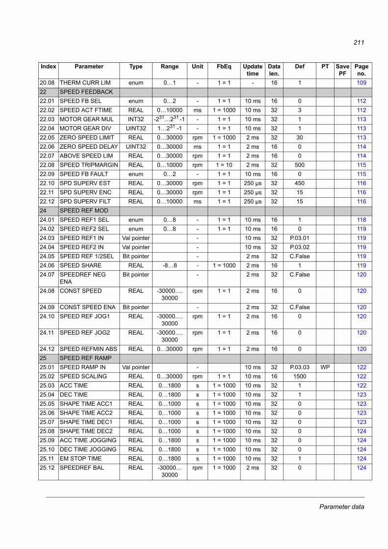
211
2222222222222222222222
2
22
2
22222222222222
0.08 THERM CURR LIM enum 0…1 - 1 = 1 - 16 1 1092 SPEED FEEDBACK2.01 SPEED FB SEL enum 0…2 - 1 = 1 10 ms 16 0 1122.02 SPEED ACT FTIME REAL 0…10000 ms 1 = 1000 10 ms 32 3 1122.03 MOTOR GEAR MUL INT32 -231…231 -1 - 1 = 1 10 ms 32 1 1132.04 MOTOR GEAR DIV UINT32 1…231 -1 - 1 = 1 10 ms 32 1 1132.05 ZERO SPEED LIMIT REAL 0…30000 rpm 1 = 1000 2 ms 32 30 1132.06 ZERO SPEED DELAY UINT32 0…30000 ms 1 = 1 2 ms 16 0 1142.07 ABOVE SPEED LIM REAL 0…30000 rpm 1 = 1 2 ms 16 0 1142.08 SPEED TRIPMARGIN REAL 0…10000 rpm 1 = 10 2 ms 32 500 1152.09 SPEED FB FAULT enum 0…2 - 1 = 1 10 ms 16 0 1152.10 SPD SUPERV EST REAL 0…30000 rpm 1 = 1 250 µs 32 450 1162.11 SPD SUPERV ENC REAL 0…30000 rpm 1 = 1 250 µs 32 15 1162.12 SPD SUPERV FILT REAL 0…10000 ms 1 = 1 250 µs 32 15 1164 SPEED REF MOD4.01 SPEED REF1 SEL enum 0…8 - 1 = 1 10 ms 16 1 1184.02 SPEED REF2 SEL enum 0…8 - 1 = 1 10 ms 16 0 1194.03 SPEED REF1 IN Val pointer - 10 ms 32 P.03.01 1194.04 SPEED REF2 IN Val pointer - 10 ms 32 P.03.02 1194.05 SPEED REF 1/2SEL Bit pointer - 2 ms 32 C.False 1194.06 SPEED SHARE REAL -8…8 - 1 = 1000 2 ms 16 1 1194.07 SPEEDREF NEG
ENABit pointer - 2 ms 32 C.False 120
4.08 CONST SPEED REAL -30000….30000
rpm 1 = 1 2 ms 16 0 120
4.09 CONST SPEED ENA Bit pointer - 2 ms 32 C.False 1204.10 SPEED REF JOG1 REAL -30000….
30000rpm 1 = 1 2 ms 16 0 120
4.11 SPEED REF JOG2 REAL -30000….30000
rpm 1 = 1 2 ms 16 0 120
4.12 SPEED REFMIN ABS REAL 0…30000 rpm 1 = 1 2 ms 16 0 1205 SPEED REF RAMP5.01 SPEED RAMP IN Val pointer - 10 ms 32 P.03.03 WP 1225.02 SPEED SCALING REAL 0…30000 rpm 1 = 1 10 ms 16 1500 1225.03 ACC TIME REAL 0…1800 s 1 = 1000 10 ms 32 1 1225.04 DEC TIME REAL 0…1800 s 1 = 1000 10 ms 32 1 1235.05 SHAPE TIME ACC1 REAL 0…1000 s 1 = 1000 10 ms 32 0 1235.06 SHAPE TIME ACC2 REAL 0…1000 s 1 = 1000 10 ms 32 0 1235.07 SHAPE TIME DEC1 REAL 0…1000 s 1 = 1000 10 ms 32 0 1235.08 SHAPE TIME DEC2 REAL 0…1000 s 1 = 1000 10 ms 32 0 1245.09 ACC TIME JOGGING REAL 0…1800 s 1 = 1000 10 ms 32 0 1245.10 DEC TIME JOGGING REAL 0…1800 s 1 = 1000 10 ms 32 0 1245.11 EM STOP TIME REAL 0…1800 s 1 = 1000 10 ms 32 1 1245.12 SPEEDREF BAL REAL -30000…
30000rpm 1 = 1000 2 ms 32 0 124
Index Parameter Type Range Unit FbEq Update time
Data len.
Def PT Save PF
Page no.
Parameter data
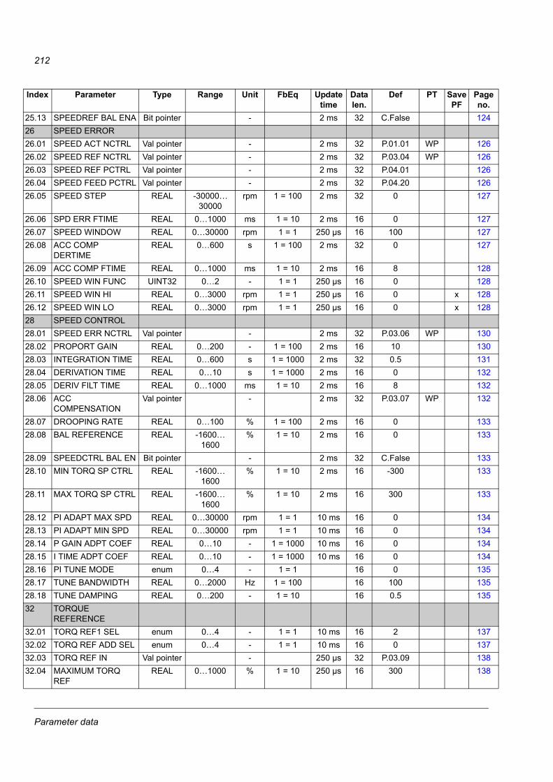
212
2222222
222
22222222222
22
22
2
22222223
3333
5.13 SPEEDREF BAL ENA Bit pointer - 2 ms 32 C.False 1246 SPEED ERROR6.01 SPEED ACT NCTRL Val pointer - 2 ms 32 P.01.01 WP 1266.02 SPEED REF NCTRL Val pointer - 2 ms 32 P.03.04 WP 1266.03 SPEED REF PCTRL Val pointer - 2 ms 32 P.04.01 1266.04 SPEED FEED PCTRL Val pointer - 2 ms 32 P.04.20 1266.05 SPEED STEP REAL -30000…
30000rpm 1 = 100 2 ms 32 0 127
6.06 SPD ERR FTIME REAL 0…1000 ms 1 = 10 2 ms 16 0 1276.07 SPEED WINDOW REAL 0…30000 rpm 1 = 1 250 µs 16 100 1276.08 ACC COMP
DERTIMEREAL 0…600 s 1 = 100 2 ms 32 0 127
6.09 ACC COMP FTIME REAL 0…1000 ms 1 = 10 2 ms 16 8 1286.10 SPEED WIN FUNC UINT32 0…2 - 1 = 1 250 µs 16 0 1286.11 SPEED WIN HI REAL 0…3000 rpm 1 = 1 250 µs 16 0 x 1286.12 SPEED WIN LO REAL 0…3000 rpm 1 = 1 250 µs 16 0 x 1288 SPEED CONTROL8.01 SPEED ERR NCTRL Val pointer - 2 ms 32 P.03.06 WP 1308.02 PROPORT GAIN REAL 0…200 - 1 = 100 2 ms 16 10 1308.03 INTEGRATION TIME REAL 0…600 s 1 = 1000 2 ms 32 0.5 1318.04 DERIVATION TIME REAL 0…10 s 1 = 1000 2 ms 16 0 1328.05 DERIV FILT TIME REAL 0…1000 ms 1 = 10 2 ms 16 8 1328.06 ACC
COMPENSATIONVal pointer - 2 ms 32 P.03.07 WP 132
8.07 DROOPING RATE REAL 0…100 % 1 = 100 2 ms 16 0 1338.08 BAL REFERENCE REAL -1600…
1600% 1 = 10 2 ms 16 0 133
8.09 SPEEDCTRL BAL EN Bit pointer - 2 ms 32 C.False 1338.10 MIN TORQ SP CTRL REAL -1600…
1600% 1 = 10 2 ms 16 -300 133
8.11 MAX TORQ SP CTRL REAL -1600…1600
% 1 = 10 2 ms 16 300 133
8.12 PI ADAPT MAX SPD REAL 0…30000 rpm 1 = 1 10 ms 16 0 1348.13 PI ADAPT MIN SPD REAL 0…30000 rpm 1 = 1 10 ms 16 0 1348.14 P GAIN ADPT COEF REAL 0…10 - 1 = 1000 10 ms 16 0 1348.15 I TIME ADPT COEF REAL 0…10 - 1 = 1000 10 ms 16 0 1348.16 PI TUNE MODE enum 0…4 - 1 = 1 16 0 1358.17 TUNE BANDWIDTH REAL 0…2000 Hz 1 = 100 16 100 1358.18 TUNE DAMPING REAL 0…200 - 1 = 10 16 0.5 1352 TORQUE
REFERENCE2.01 TORQ REF1 SEL enum 0…4 - 1 = 1 10 ms 16 2 1372.02 TORQ REF ADD SEL enum 0…4 - 1 = 1 10 ms 16 0 1372.03 TORQ REF IN Val pointer - 250 µs 32 P.03.09 1382.04 MAXIMUM TORQ
REFREAL 0…1000 % 1 = 10 250 µs 16 300 138
Index Parameter Type Range Unit FbEq Update time
Data len.
Def PT Save PF
Page no.
Parameter data
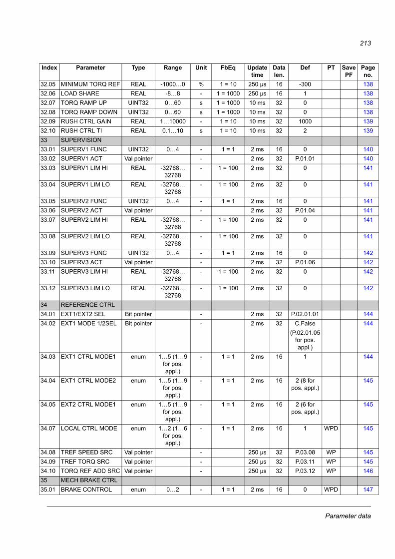
213
3333333333
3
333
3
333
3
333
3
3
3
3
33333
2.05 MINIMUM TORQ REF REAL -1000…0 % 1 = 10 250 µs 16 -300 1382.06 LOAD SHARE REAL -8…8 - 1 = 1000 250 µs 16 1 1382.07 TORQ RAMP UP UINT32 0…60 s 1 = 1000 10 ms 32 0 1382.08 TORQ RAMP DOWN UINT32 0…60 s 1 = 1000 10 ms 32 0 1382.09 RUSH CTRL GAIN REAL 1…10000 - 1 = 10 10 ms 32 1000 1392.10 RUSH CTRL TI REAL 0.1…10 s 1 = 10 10 ms 32 2 1393 SUPERVISION3.01 SUPERV1 FUNC UINT32 0…4 - 1 = 1 2 ms 16 0 1403.02 SUPERV1 ACT Val pointer - 2 ms 32 P.01.01 1403.03 SUPERV1 LIM HI REAL -32768…
32768- 1 = 100 2 ms 32 0 141
3.04 SUPERV1 LIM LO REAL -32768… 32768
- 1 = 100 2 ms 32 0 141
3.05 SUPERV2 FUNC UINT32 0…4 - 1 = 1 2 ms 16 0 1413.06 SUPERV2 ACT Val pointer - 2 ms 32 P.01.04 1413.07 SUPERV2 LIM HI REAL -32768…
32768- 1 = 100 2 ms 32 0 141
3.08 SUPERV2 LIM LO REAL -32768… 32768
- 1 = 100 2 ms 32 0 141
3.09 SUPERV3 FUNC UINT32 0…4 - 1 = 1 2 ms 16 0 1423.10 SUPERV3 ACT Val pointer - 2 ms 32 P.01.06 1423.11 SUPERV3 LIM HI REAL -32768…
32768- 1 = 100 2 ms 32 0 142
3.12 SUPERV3 LIM LO REAL -32768… 32768
- 1 = 100 2 ms 32 0 142
4 REFERENCE CTRL4.01 EXT1/EXT2 SEL Bit pointer - 2 ms 32 P.02.01.01 1444.02 EXT1 MODE 1/2SEL Bit pointer - 2 ms 32 C.False
(P.02.01.05 for pos. appl.)
144
4.03 EXT1 CTRL MODE1 enum 1…5 (1…9 for pos. appl.)
- 1 = 1 2 ms 16 1 144
4.04 EXT1 CTRL MODE2 enum 1…5 (1…9 for pos. appl.)
- 1 = 1 2 ms 16 2 (8 for pos. appl.)
145
4.05 EXT2 CTRL MODE1 enum 1…5 (1…9 for pos. appl.)
- 1 = 1 2 ms 16 2 (6 for pos. appl.)
145
4.07 LOCAL CTRL MODE enum 1…2 (1…6 for pos. appl.)
- 1 = 1 2 ms 16 1 WPD 145
4.08 TREF SPEED SRC Val pointer - 250 µs 32 P.03.08 WP 1454.09 TREF TORQ SRC Val pointer - 250 µs 32 P.03.11 WP 1454.10 TORQ REF ADD SRC Val pointer - 250 µs 32 P.03.12 WP 1465 MECH BRAKE CTRL5.01 BRAKE CONTROL enum 0…2 - 1 = 1 2 ms 16 0 WPD 147
Index Parameter Type Range Unit FbEq Update time
Data len.
Def PT Save PF
Page no.
Parameter data
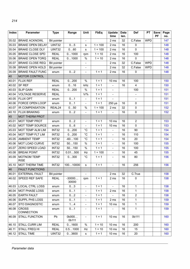
214
333333334444444444444444444
4444
444444
4
444
5.02 BRAKE ACKNOWL Bit pointer - 2 ms 32 C.False WPD 1475.03 BRAKE OPEN DELAY UINT32 0…5 s 1 = 100 2 ms 16 0 1485.04 BRAKE CLOSE DLY UINT32 0…60 s 1 = 100 2 ms 16 0 1485.05 BRAKE CLOSE SPD REAL 0…1000 rpm 1 = 10 2 ms 16 100 1485.06 BRAKE OPEN TORQ REAL 0…1000 % 1 = 10 2 ms 16 0 1485.07 BRAKE CLOSE REQ Bit pointer - 2 ms 32 C.False WPD 1485.08 BRAKE OPEN HOLD Bit pointer - 2 ms 32 C.False WPD 1485.09 BRAKE FAULT FUNC enum 0…2 - 1 = 1 2 ms 16 0 1480 MOTOR CONTROL0.01 FLUX REF REAL 0…200 % 1 = 1 10 ms 16 100 1500.02 SF REF enum 0…16 kHz 1 = 1 - 16 4 1500.03 SLIP GAIN REAL 0…200 % 1 = 1 - 100 1510.04 VOLTAGE RESERVE REAL V/% 1 = 1 - - 1510.05 FLUX OPT enum 0…1 - 1 = 1 - - 1510.06 FORCE OPEN LOOP enum 0…1 - 1 = 1 250 µs 16 0 1510.07 IR COMPENSATION REAL24 0…50 % 1 = 100 2 ms 32 0 1520.10 FLUX BRAKING enum 0…2 - 1 = 1 - 16 0 1525 MOT THERM PROT5.01 MOT TEMP PROT enum 0…2 - 1 = 1 10 ms 16 2 1535.02 MOT TEMP SOURCE enum 0…6 - 1 = 1 10 ms 16 0 1535.03 MOT TEMP ALM LIM INT32 0…200 °C 1 = 1 - 16 90 1545.04 MOT TEMP FLT LIM INT32 0…200 °C 1 = 1 - 16 110 1545.05 AMBIENT TEMP INT32 -60…100 °C 1 = 1 - 16 20 1545.06 MOT LOAD CURVE INT32 50…150 % 1 = 1 - 16 100 1555.07 ZERO SPEED LOAD INT32 50…150 % 1 = 1 - 16 100 1555.08 BREAK POINT INT32 0.01…500 Hz 1 = 100 - 16 45 1555.09 MOTNOM TEMP
RISEINT32 0…300 °C 1 = 1 - 16 80 156
5.10 MOT THERM TIME INT32 100…10000 s 1 = 1 - 16 256 1566 FAULT FUNCTIONS6.01 EXTERNAL FAULT Bit pointer - 2 ms 32 C.True 1586.02 SPEED REF SAFE REAL -30000…
30000rpm 1 = 1 2 ms 16 0 158
6.03 LOCAL CTRL LOSS enum 0…3 - 1 = 1 - 16 1 1586.04 MOT PHASE LOSS enum 0…1 - 1 = 1 2 ms 16 1 1586.05 EARTH FAULT enum 0…2 - 1 = 1 - 16 2 1586.06 SUPPL PHS LOSS enum 0…1 - 1 = 1 2 ms 16 1 1596.07 STO DIAGNOSTIC enum 1…4 - 1 = 1 10 ms 16 1 1596.08 CROSS
CONNECTIONenum 0…1 - 1 = 1 - 16 1 159
6.09 STALL FUNCTION Pb 0b000…0b111
- 1 = 1 10 ms 16 0b111 160
6.10 STALL CURR LIM REAL 0…1600 % 1 = 10 10 ms 16 200 1606.11 STALL FREQ HI REAL 0.5…1000 Hz 1 = 10 10 ms 16 15 1606.12 STALL TIME UINT32 0…3600 s 1 = 1 10 ms 16 20 160
Index Parameter Type Range Unit FbEq Update time
Data len.
Def PT Save PF
Page no.
Parameter data

215
44
44444444444
4
44455555
5
55555555
555…555
7 VOLTAGE CTRL7.01 OVERVOLTAGE
CTRLenum 0…1 - 1 = 1 10 ms 16 1 161
7.02 UNDERVOLT CTRL enum 0…1 - 1 = 1 10 ms 16 1 1617.03 SUPPLVOLTAUTO-ID enum 0…1 - 1 = 1 10 ms 16 1 1617.04 SUPPLY VOLTAGE REAL 0…1000 V 1 = 10 2 ms 16 400 1627.05 LOW VOLT MOD ENA Bit pointer - 32 C.False 1627.06 LOW VOLT DC MIN REAL 250…450 V 1 = 1 10 ms 16 250 1627.07 LOW VOLT DC MAX REAL 350…810 V 1 = 1 10 ms 16 810 1627.08 EXT PU SUPPLY Bit pointer - 32 C.False 1628 BRAKE CHOPPER8.01 BC ENABLE enum 0…2 - 1 = 1 - 16 0 1638.02 BC RUN-TIME ENA Bit pointer - 2 ms 32 P.06.01.03 1638.03 BRTHERMTIMECON
STREAL24 0…10000 s 1 = 1 - 32 0 163
8.04 BR POWER MAX CNT
REAL24 0…10000 kW 1 = 10000 - 32 0 163
8.05 R BR REAL24 0.1…1000 ohm 1 = 10000 - 32 - 1638.06 BR TEMP FAULTLIM REAL24 0…150 % 1 = 1 - 16 105 1648.07 BR TEMP ALARMLIM REAL24 0…150 % 1 = 1 - 16 95 1640 FIELDBUS0.01 FBA ENABLE enum 0…1 - 1 = 1 - 16 0 1650.02 COMM LOSS FUNC enum 0…3 - 1 = 1 - 16 0 1650.03 COMM LOSS T OUT UINT32 0.3…6553.5 s 1 = 10 - 16 0.3 1660.04 FBA REF1 MODESEL enum 0…2 (0…4
for pos. appl.)
- 1 = 1 10 ms 16 2 166
0.05 FBA REF2 MODESEL enum 0…2 (0…4 for pos. appl.)
- 1 = 1 10 ms 16 3 166
0.06 FBA ACT1 TR SRC Val pointer - 10 ms 32 P.01.01 1660.07 FBA ACT2 TR SRC Val pointer - 10 ms 32 P.01.06 1660.08 FBA SW B12 SRC Bit pointer - 500 µs 32 C.False 1670.09 FBA SW B13 SRC Bit pointer - 500 µs 32 C.False 1670.10 FBA SW B14 SRC Bit pointer - 500 µs 32 C.False 1670.11 FBA SW B15 SRC Bit pointer - 500 µs 32 C.False 1670.12 FBA CYCLE TIME enum 0…2 - 1 = 1 10 ms 16 2 1670.20 FB MAIN SW FUNC Pb 0b000…
0b111- 1 = 1 10 ms 16 0b001 168
1 FBA SETTINGS1.01 FBA TYPE UINT32 0…65536 - 1 = 1 16 0 1691.02 FBA PAR2 UINT32 0…65536 - 1 = 1 16 0 x 169
… … … … … …. …1.26 FBA PAR26 UINT32 0…65536 - 1 = 1 16 0 x 1691.27 FBA PAR REFRESH UINT32 0…1 - 1 = 1 16 0 WPD x 1691.28 PAR TABLE VER UINT32 0…65536 - 1 = 1 16 0 x 169
Index Parameter Type Range Unit FbEq Update time
Data len.
Def PT Save PF
Page no.
Parameter data
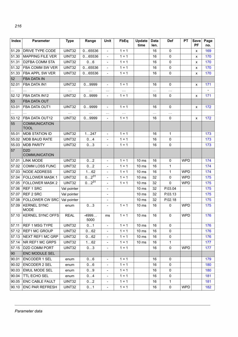
216
5555555…555…55
5555
555555555
5
555559999999
1.29 DRIVE TYPE CODE UINT32 0…65536 - 1 = 1 16 0 x 1691.30 MAPPING FILE VER UINT32 0…65536 - 1 = 1 16 0 x 1701.31 D2FBA COMM STA UINT32 0…6 - 1 = 1 16 0 x 1701.32 FBA COMM SW VER UINT32 0…65536 - 1 = 1 16 0 x 1701.33 FBA APPL SW VER UINT32 0…65536 - 1 = 1 16 0 x 1702 FBA DATA IN2.01 FBA DATA IN1 UINT32 0…9999 - 1 = 1 16 0 x 171
… … … … … … … -2.12 FBA DATA IN12 UINT32 0…9999 - 1 = 1 16 0 x 1713 FBA DATA OUT3.01 FBA DATA OUT1 UINT32 0…9999 - 1 = 1 16 0 x 172
… … … … … … …3.12 FBA DATA OUT12 UINT32 0…9999 - 1 = 1 16 0 x 1725 COMMUNICATION
TOOL5.01 MDB STATION ID UINT32 1…247 - 1 = 1 16 1 1735.02 MDB BAUD RATE UINT32 0…4 - 1 = 1 16 0 1735.03 MDB PARITY UINT32 0…3 - 1 = 1 16 0 1737 D2D
COMMUNICATION7.01 LINK MODE UINT32 0…2 - 1 = 1 10 ms 16 0 WPD 1747.02 COMM LOSS FUNC UINT32 0…2 - 1 = 1 10 ms 16 1 1747.03 NODE ADDRESS UINT32 1…62 - 1 = 1 10 ms 16 1 WPD 1747.04 FOLLOWER MASK 1 UINT32 0…231 - 1 = 1 10 ms 32 0 WPD 1757.05 FOLLOWER MASK 2 UINT32 0…231 - 1 = 1 10 ms 32 0 WPD 1757.06 REF 1 SRC Val pointer - 10 ms 32 P.03.04 1757.07 REF 2 SRC Val pointer - 10 ms 32 P.03.13 1757.08 FOLLOWER CW SRC Val pointer - 10 ms 32 P.02.18 1757.09 KERNEL SYNC
MODEenum 0…3 - 1 = 1 10 ms 16 0 WPD 175
7.10 KERNEL SYNC OFFS REAL -4999…5000
ms 1 = 1 10 ms 16 0 WPD 176
7.11 REF 1 MSG TYPE UINT32 0…1 - 1 = 1 10 ms 16 0 1767.12 REF1 MC GROUP UINT32 0…62 - 1 = 1 10 ms 16 0 1767.13 NEXT REF1 MC GRP UINT32 0…62 - 1 = 1 10 ms 16 0 1767.14 NR REF1 MC GRPS UINT32 1…62 - 1 = 1 10 ms 16 1 1777.15 D2D COMM PORT UINT32 0…3 - 1 = 1 16 0 WPD 1770 ENC MODULE SEL0.01 ENCODER 1 SEL enum 0…6 - 1 = 1 16 0 1790.02 ENCODER 2 SEL enum 0…6 - 1 = 1 16 0 1800.03 EMUL MODE SEL enum 0…9 - 1 = 1 16 0 1800.04 TTL ECHO SEL enum 0…4 - 1 = 1 16 0 1810.05 ENC CABLE FAULT UINT32 0…2 - 1 = 1 16 1 1810.10 ENC PAR REFRESH UINT32 0…1 - 1 = 1 16 0 WPD 182
Index Parameter Type Range Unit FbEq Update time
Data len.
Def PT Save PF
Page no.
Parameter data

217
9999999999999999999999999999
999999
99999
9
1 ABSOL ENC CONF1.01 SINE COSINE NR UINT32 0…65535 - 1 = 1 16 0 1841.02 ABS ENC INTERF UINT32 0…4 - 1 = 1 16 0 1841.03 REV COUNT BITS UINT32 0…32 - 1 = 1 16 0 1841.04 POS DATA BITS UINT32 0…32 - 1 = 1 16 0 1841.05 REFMARK ENA UINT32 0…1 - 1 = 1 16 0 1841.06 ABS POS TRACKING UINT32 0…1 - 1 = 1 16 0 1851.10 HIPERFACE PARITY UINT32 0…1 - 1 = 1 16 0 1851.11 HIPERF BAUDRATE UINT32 0…3 - 1 = 1 16 1 1851.12 HIPERF NODE ADDR UINT32 0…255 - 1 = 1 16 64 1851.20 SSI CLOCK CYCLES UINT32 2…127 - 1 = 1 16 2 1851.21 SSI POSITION MSB UINT32 1…126 - 1 = 1 16 1 1861.22 SSI REVOL MSB UINT32 1…126 - 1 = 1 16 1 1861.23 SSI DATA FORMAT UINT32 0…1 - 1 = 1 16 0 1861.24 SSI BAUD RATE UINT32 0…5 - 1 = 1 16 2 1861.25 SSI MODE UINT32 0…1 - 1 = 1 16 0 1861.26 SSI TRANSMIT CYC UINT32 0…5 - 1 = 1 16 1 1861.27 SSI ZERO PHASE UINT32 0…3 - 1 = 1 16 0 1871.30 ENDAT MODE UINT32 0…1 - 1 = 1 16 0 1871.31 ENDAT MAX CALC UINT32 0…3 - 1 = 1 16 3 1872 RESOLVER CONF2.01 RESOLV POLEPAIRS UINT32 1…32 - 1 = 1 16 1 1882.02 EXC SIGNAL AMPL UINT32 4…12 Vrms 1 = 10 16 4 1882.03 EXC SIGNAL FREQ UINT32 1…20 kHz 1 = 1 16 1 1883 PULSE ENC CONF3.01 ENC1 PULSE NR UINT32 0…65535 - 1 = 1 16 0 1893.02 ENC1 TYPE enum 0…1 - 1 = 1 16 0 1893.03 ENC1 SP
CALCMODEenum 0….5 - 1 = 1 16 4 189
3.04 ENC1 POS EST ENA enum 0…1 - 1 = 1 16 1 1903.05 ENC1 SP EST ENA enum 0…1 - 1 = 1 16 0 1903.06 ENC1 OSC LIM enum 0…3 - 1 = 1 16 0 1903.11 ENC2 PULSE NR UINT32 0…65535 - 1 = 1 16 0 1913.12 ENC2 TYPE enum 0…1 - 1 = 1 16 0 1913.13 ENC2 SP
CALCMODEenum 0….5 - 1 = 1 16 4 191
3.14 ENC2 POS EST ENA enum 0…1 - 1 = 1 16 1 1913.15 ENC2 SP EST ENA enum 0…1 - 1 = 1 16 0 1913.16 ENC2 OSC LIM enum 0…3 - 1 = 1 16 0 1913.21 EMUL PULSE NR UINT32 0…65535 - 1 = 1 16 0 1913.22 EMUL POS REF Val pointer - 32 P.01.12
(P.04.17 for pos. appl.)
191
3.23 EMUL POS OFFSET REAL 0 … 0.99998
rev 1 = 100000 32 0 191
Index Parameter Type Range Unit FbEq Update time
Data len.
Def PT Save PF
Page no.
Parameter data
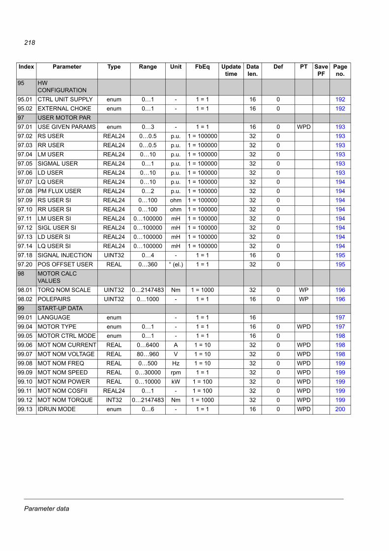
218
9
99999999999999999999
99999999999999
5 HW CONFIGURATION
5.01 CTRL UNIT SUPPLY enum 0…1 - 1 = 1 16 0 1925.02 EXTERNAL CHOKE enum 0…1 - 1 = 1 16 0 1927 USER MOTOR PAR7.01 USE GIVEN PARAMS enum 0…3 - 1 = 1 16 0 WPD 1937.02 RS USER REAL24 0…0.5 p.u. 1 = 100000 32 0 1937.03 RR USER REAL24 0…0.5 p.u. 1 = 100000 32 0 1937.04 LM USER REAL24 0…10 p.u. 1 = 100000 32 0 1937.05 SIGMAL USER REAL24 0…1 p.u. 1 = 100000 32 0 1937.06 LD USER REAL24 0…10 p.u. 1 = 100000 32 0 1937.07 LQ USER REAL24 0…10 p.u. 1 = 100000 32 0 1947.08 PM FLUX USER REAL24 0…2 p.u. 1 = 100000 32 0 1947.09 RS USER SI REAL24 0…100 ohm 1 = 100000 32 0 1947.10 RR USER SI REAL24 0…100 ohm 1 = 100000 32 0 1947.11 LM USER SI REAL24 0…100000 mH 1 = 100000 32 0 1947.12 SIGL USER SI REAL24 0…100000 mH 1 = 100000 32 0 1947.13 LD USER SI REAL24 0…100000 mH 1 = 100000 32 0 1947.14 LQ USER SI REAL24 0…100000 mH 1 = 100000 32 0 1947.18 SIGNAL INJECTION UINT32 0…4 - 1 = 1 16 0 1957.20 POS OFFSET USER REAL 0…360 ° (el.) 1 = 1 32 0 1958 MOTOR CALC
VALUES8.01 TORQ NOM SCALE UINT32 0…2147483 Nm 1 = 1000 32 0 WP 1968.02 POLEPAIRS UINT32 0…1000 - 1 = 1 16 0 WP 1969 START-UP DATA9.01 LANGUAGE enum - 1 = 1 16 1979.04 MOTOR TYPE enum 0…1 - 1 = 1 16 0 WPD 1979.05 MOTOR CTRL MODE enum 0…1 - 1 = 1 16 0 1989.06 MOT NOM CURRENT REAL 0…6400 A 1 = 10 32 0 WPD 1989.07 MOT NOM VOLTAGE REAL 80…960 V 1 = 10 32 0 WPD 1989.08 MOT NOM FREQ REAL 0…500 Hz 1 = 10 32 0 WPD 1999.09 MOT NOM SPEED REAL 0…30000 rpm 1 = 1 32 0 WPD 1999.10 MOT NOM POWER REAL 0…10000 kW 1 = 100 32 0 WPD 1999.11 MOT NOM COSFII REAL24 0…1 - 1 = 100 32 0 WPD 1999.12 MOT NOM TORQUE INT32 0…2147483 Nm 1 = 1000 32 0 WPD 1999.13 IDRUN MODE enum 0…6 - 1 = 1 16 0 WPD 200
Index Parameter Type Range Unit FbEq Update time
Data len.
Def PT Save PF
Page no.
Parameter data
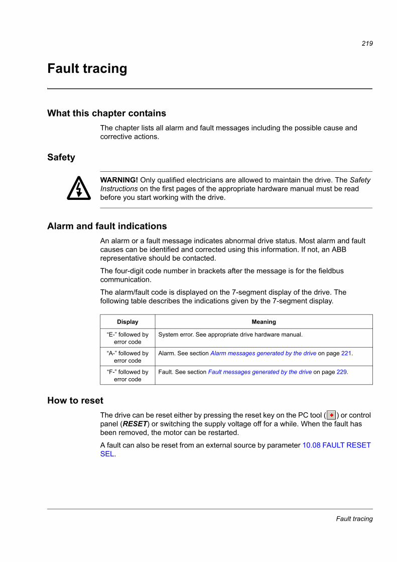
219
Fault tracing
What this chapter containsThe chapter lists all alarm and fault messages including the possible cause and corrective actions.
Safety
WARNING! Only qualified electricians are allowed to maintain the drive. The Safety Instructions on the first pages of the appropriate hardware manual must be read before you start working with the drive.
Alarm and fault indicationsAn alarm or a fault message indicates abnormal drive status. Most alarm and fault causes can be identified and corrected using this information. If not, an ABB representative should be contacted.
The four-digit code number in brackets after the message is for the fieldbus communication.
The alarm/fault code is displayed on the 7-segment display of the drive. The following table describes the indications given by the 7-segment display.
How to resetThe drive can be reset either by pressing the reset key on the PC tool ( ) or control panel (RESET) or switching the supply voltage off for a while. When the fault has been removed, the motor can be restarted.
A fault can also be reset from an external source by parameter 10.08 FAULT RESET SEL.
Display Meaning
“E-” followed by error code
System error. See appropriate drive hardware manual.
“A-” followed by error code
Alarm. See section Alarm messages generated by the drive on page 221.
“F-” followed by error code
Fault. See section Fault messages generated by the drive on page 229.
Fault tracing

220
Fault historyWhen a fault is detected, it is stored in the fault logger with a time stamp. The fault history stores information on the 16 latest faults of the drive. Three of the latest faults are stored at the beginning of a power switch off.
Signals 8.01 ACTIVE FAULT and 8.02 LAST FAULT store the fault codes of the most recent faults.
Alarms can be monitored via bit words 8.05 ALARM LOGGER 1…8.10 ALARM LOGGER 6 and 8.15 ALARM WORD 1…8.18 ALARM WORD 4. Alarm information is lost at power switch off or fault reset.
Fault tracing
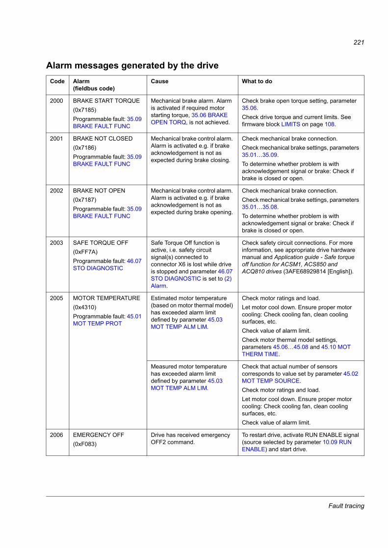
221
Alarm messages generated by the driveCode Alarm
(fieldbus code)Cause What to do
2000 BRAKE START TORQUE(0x7185)Programmable fault: 35.09 BRAKE FAULT FUNC
Mechanical brake alarm. Alarm is activated if required motor starting torque, 35.06 BRAKE OPEN TORQ, is not achieved.
Check brake open torque setting, parameter 35.06.Check drive torque and current limits. See firmware block LIMITS on page 108.
2001 BRAKE NOT CLOSED(0x7186)Programmable fault: 35.09 BRAKE FAULT FUNC
Mechanical brake control alarm. Alarm is activated e.g. if brake acknowledgement is not as expected during brake closing.
Check mechanical brake connection.Check mechanical brake settings, parameters 35.01…35.09.To determine whether problem is with acknowledgement signal or brake: Check if brake is closed or open.
2002 BRAKE NOT OPEN(0x7187)Programmable fault: 35.09 BRAKE FAULT FUNC
Mechanical brake control alarm. Alarm is activated e.g. if brake acknowledgement is not as expected during brake opening.
Check mechanical brake connection.Check mechanical brake settings, parameters 35.01…35.08.To determine whether problem is with acknowledgement signal or brake: Check if brake is closed or open.
2003 SAFE TORQUE OFF(0xFF7A)Programmable fault: 46.07 STO DIAGNOSTIC
Safe Torque Off function is active, i.e. safety circuit signal(s) connected to connector X6 is lost while drive is stopped and parameter 46.07 STO DIAGNOSTIC is set to (2) Alarm.
Check safety circuit connections. For more information, see appropriate drive hardware manual and Application guide - Safe torque off function for ACSM1, ACS850 and ACQ810 drives (3AFE68929814 [English]).
2005 MOTOR TEMPERATURE(0x4310)Programmable fault: 45.01 MOT TEMP PROT
Estimated motor temperature (based on motor thermal model) has exceeded alarm limit defined by parameter 45.03 MOT TEMP ALM LIM.
Check motor ratings and load.Let motor cool down. Ensure proper motor cooling: Check cooling fan, clean cooling surfaces, etc.Check value of alarm limit.Check motor thermal model settings, parameters 45.06…45.08 and 45.10 MOT THERM TIME.
Measured motor temperature has exceeded alarm limit defined by parameter 45.03 MOT TEMP ALM LIM.
Check that actual number of sensors corresponds to value set by parameter 45.02 MOT TEMP SOURCE.Check motor ratings and load.Let motor cool down. Ensure proper motor cooling: Check cooling fan, clean cooling surfaces, etc.Check value of alarm limit.
2006 EMERGENCY OFF(0xF083)
Drive has received emergency OFF2 command.
To restart drive, activate RUN ENABLE signal (source selected by parameter 10.09 RUN ENABLE) and start drive.
Fault tracing
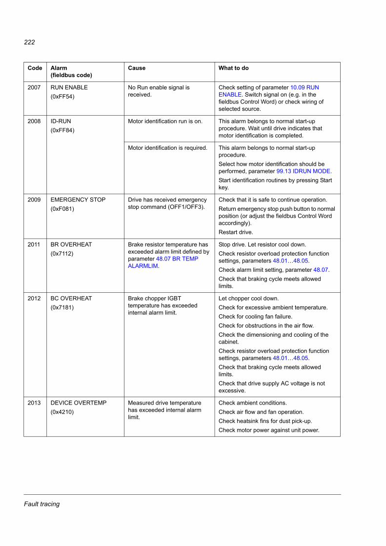
222
2007 RUN ENABLE(0xFF54)
No Run enable signal is received.
Check setting of parameter 10.09 RUN ENABLE. Switch signal on (e.g. in the fieldbus Control Word) or check wiring of selected source.
2008 ID-RUN(0xFF84)
Motor identification run is on. This alarm belongs to normal start-up procedure. Wait until drive indicates that motor identification is completed.
Motor identification is required. This alarm belongs to normal start-up procedure. Select how motor identification should be performed, parameter 99.13 IDRUN MODE.Start identification routines by pressing Start key.
2009 EMERGENCY STOP(0xF081)
Drive has received emergency stop command (OFF1/OFF3).
Check that it is safe to continue operation.Return emergency stop push button to normal position (or adjust the fieldbus Control Word accordingly).Restart drive.
2011 BR OVERHEAT(0x7112)
Brake resistor temperature has exceeded alarm limit defined by parameter 48.07 BR TEMP ALARMLIM.
Stop drive. Let resistor cool down.Check resistor overload protection function settings, parameters 48.01…48.05.Check alarm limit setting, parameter 48.07.Check that braking cycle meets allowed limits.
2012 BC OVERHEAT(0x7181)
Brake chopper IGBT temperature has exceeded internal alarm limit.
Let chopper cool down.Check for excessive ambient temperature.Check for cooling fan failure.Check for obstructions in the air flow.Check the dimensioning and cooling of the cabinet.Check resistor overload protection function settings, parameters 48.01…48.05.Check that braking cycle meets allowed limits.Check that drive supply AC voltage is not excessive.
2013 DEVICE OVERTEMP(0x4210)
Measured drive temperature has exceeded internal alarm limit.
Check ambient conditions.Check air flow and fan operation.Check heatsink fins for dust pick-up.Check motor power against unit power.
Code Alarm(fieldbus code)
Cause What to do
Fault tracing
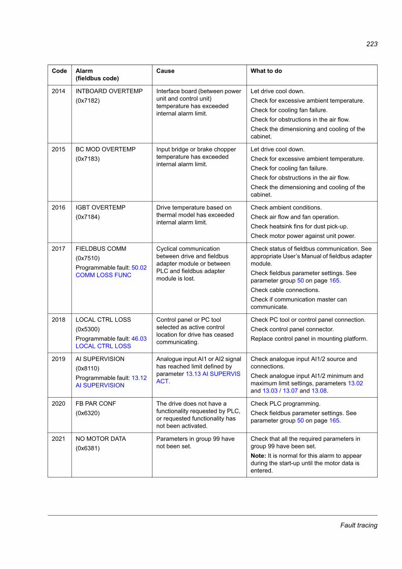
223
2014 INTBOARD OVERTEMP(0x7182)
Interface board (between power unit and control unit) temperature has exceeded internal alarm limit.
Let drive cool down.Check for excessive ambient temperature.Check for cooling fan failure.Check for obstructions in the air flow.Check the dimensioning and cooling of the cabinet.
2015 BC MOD OVERTEMP(0x7183)
Input bridge or brake chopper temperature has exceeded internal alarm limit.
Let drive cool down.Check for excessive ambient temperature.Check for cooling fan failure.Check for obstructions in the air flow.Check the dimensioning and cooling of the cabinet.
2016 IGBT OVERTEMP(0x7184)
Drive temperature based on thermal model has exceeded internal alarm limit.
Check ambient conditions.Check air flow and fan operation.Check heatsink fins for dust pick-up.Check motor power against unit power.
2017 FIELDBUS COMM(0x7510)Programmable fault: 50.02 COMM LOSS FUNC
Cyclical communication between drive and fieldbus adapter module or between PLC and fieldbus adapter module is lost.
Check status of fieldbus communication. See appropriate User’s Manual of fieldbus adapter module.Check fieldbus parameter settings. See parameter group 50 on page 165.Check cable connections.Check if communication master can communicate.
2018 LOCAL CTRL LOSS(0x5300)Programmable fault: 46.03 LOCAL CTRL LOSS
Control panel or PC tool selected as active control location for drive has ceased communicating.
Check PC tool or control panel connection.Check control panel connector.Replace control panel in mounting platform.
2019 AI SUPERVISION(0x8110)Programmable fault: 13.12 AI SUPERVISION
Analogue input AI1 or AI2 signal has reached limit defined by parameter 13.13 AI SUPERVIS ACT.
Check analogue input AI1/2 source and connections. Check analogue input AI1/2 minimum and maximum limit settings, parameters 13.02 and 13.03 / 13.07 and 13.08.
2020 FB PAR CONF(0x6320)
The drive does not have a functionality requested by PLC, or requested functionality has not been activated.
Check PLC programming.Check fieldbus parameter settings. See parameter group 50 on page 165.
2021 NO MOTOR DATA(0x6381)
Parameters in group 99 have not been set.
Check that all the required parameters in group 99 have been set.Note: It is normal for this alarm to appear during the start-up until the motor data is entered.
Code Alarm(fieldbus code)
Cause What to do
Fault tracing
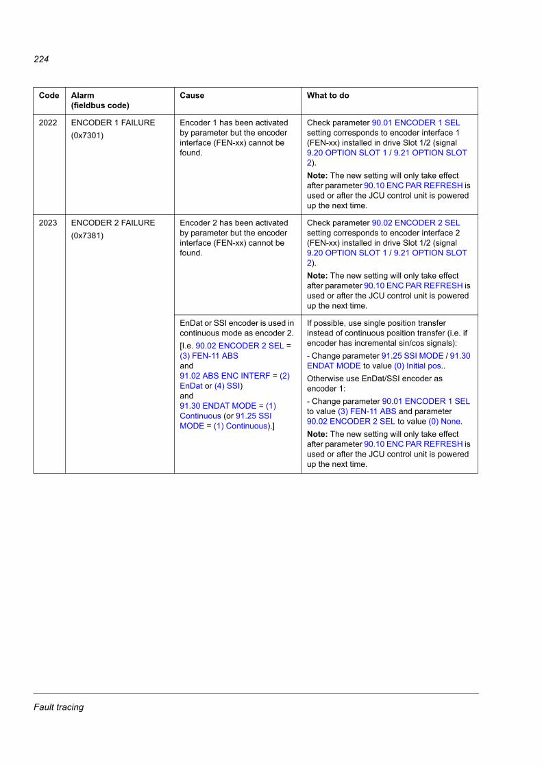
224
2022 ENCODER 1 FAILURE(0x7301)
Encoder 1 has been activated by parameter but the encoder interface (FEN-xx) cannot be found.
Check parameter 90.01 ENCODER 1 SEL setting corresponds to encoder interface 1 (FEN-xx) installed in drive Slot 1/2 (signal 9.20 OPTION SLOT 1 / 9.21 OPTION SLOT 2).Note: The new setting will only take effect after parameter 90.10 ENC PAR REFRESH is used or after the JCU control unit is powered up the next time.
2023 ENCODER 2 FAILURE(0x7381)
Encoder 2 has been activated by parameter but the encoder interface (FEN-xx) cannot be found.
Check parameter 90.02 ENCODER 2 SEL setting corresponds to encoder interface 2 (FEN-xx) installed in drive Slot 1/2 (signal 9.20 OPTION SLOT 1 / 9.21 OPTION SLOT 2).Note: The new setting will only take effect after parameter 90.10 ENC PAR REFRESH is used or after the JCU control unit is powered up the next time.
EnDat or SSI encoder is used in continuous mode as encoder 2. [I.e. 90.02 ENCODER 2 SEL = (3) FEN-11 ABSand91.02 ABS ENC INTERF = (2) EnDat or (4) SSI)and91.30 ENDAT MODE = (1) Continuous (or 91.25 SSI MODE = (1) Continuous).]
If possible, use single position transfer instead of continuous position transfer (i.e. if encoder has incremental sin/cos signals):- Change parameter 91.25 SSI MODE / 91.30 ENDAT MODE to value (0) Initial pos..Otherwise use EnDat/SSI encoder as encoder 1:- Change parameter 90.01 ENCODER 1 SEL to value (3) FEN-11 ABS and parameter 90.02 ENCODER 2 SEL to value (0) None.Note: The new setting will only take effect after parameter 90.10 ENC PAR REFRESH is used or after the JCU control unit is powered up the next time.
Code Alarm(fieldbus code)
Cause What to do
Fault tracing
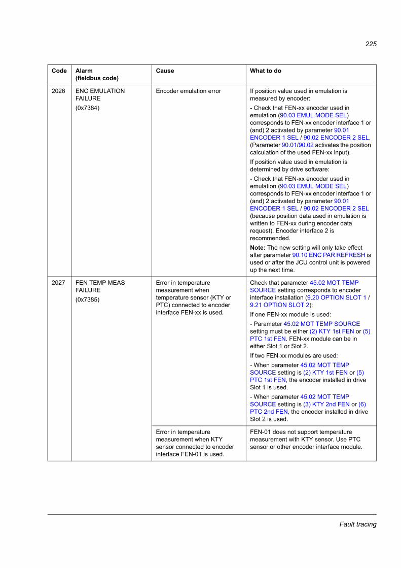
225
2026 ENC EMULATION FAILURE(0x7384)
Encoder emulation error If position value used in emulation is measured by encoder:- Check that FEN-xx encoder used in emulation (90.03 EMUL MODE SEL) corresponds to FEN-xx encoder interface 1 or (and) 2 activated by parameter 90.01 ENCODER 1 SEL / 90.02 ENCODER 2 SEL. (Parameter 90.01/90.02 activates the position calculation of the used FEN-xx input).If position value used in emulation is determined by drive software:- Check that FEN-xx encoder used in emulation (90.03 EMUL MODE SEL) corresponds to FEN-xx encoder interface 1 or (and) 2 activated by parameter 90.01 ENCODER 1 SEL / 90.02 ENCODER 2 SEL (because position data used in emulation is written to FEN-xx during encoder data request). Encoder interface 2 is recommended.Note: The new setting will only take effect after parameter 90.10 ENC PAR REFRESH is used or after the JCU control unit is powered up the next time.
2027 FEN TEMP MEAS FAILURE(0x7385)
Error in temperature measurement when temperature sensor (KTY or PTC) connected to encoder interface FEN-xx is used.
Check that parameter 45.02 MOT TEMP SOURCE setting corresponds to encoder interface installation (9.20 OPTION SLOT 1 / 9.21 OPTION SLOT 2):If one FEN-xx module is used:- Parameter 45.02 MOT TEMP SOURCE setting must be either (2) KTY 1st FEN or (5) PTC 1st FEN. FEN-xx module can be in either Slot 1 or Slot 2.If two FEN-xx modules are used: - When parameter 45.02 MOT TEMP SOURCE setting is (2) KTY 1st FEN or (5) PTC 1st FEN, the encoder installed in drive Slot 1 is used.- When parameter 45.02 MOT TEMP SOURCE setting is (3) KTY 2nd FEN or (6) PTC 2nd FEN, the encoder installed in drive Slot 2 is used.
Error in temperature measurement when KTY sensor connected to encoder interface FEN-01 is used.
FEN-01 does not support temperature measurement with KTY sensor. Use PTC sensor or other encoder interface module.
Code Alarm(fieldbus code)
Cause What to do
Fault tracing
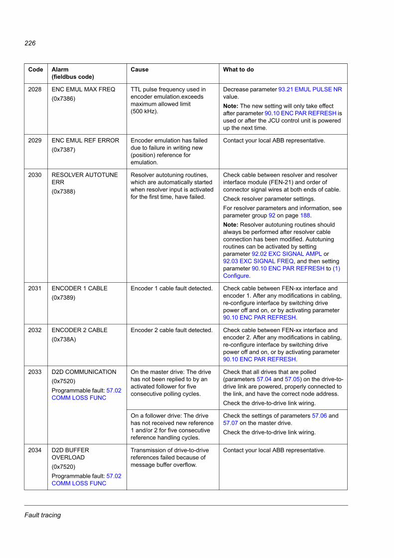
226
2028 ENC EMUL MAX FREQ(0x7386)
TTL pulse frequency used in encoder emulation.exceeds maximum allowed limit (500 kHz).
Decrease parameter 93.21 EMUL PULSE NR value. Note: The new setting will only take effect after parameter 90.10 ENC PAR REFRESH is used or after the JCU control unit is powered up the next time.
2029 ENC EMUL REF ERROR(0x7387)
Encoder emulation has failed due to failure in writing new (position) reference for emulation.
Contact your local ABB representative.
2030 RESOLVER AUTOTUNE ERR(0x7388)
Resolver autotuning routines, which are automatically started when resolver input is activated for the first time, have failed.
Check cable between resolver and resolver interface module (FEN-21) and order of connector signal wires at both ends of cable.Check resolver parameter settings.For resolver parameters and information, see parameter group 92 on page 188.Note: Resolver autotuning routines should always be performed after resolver cable connection has been modified. Autotuning routines can be activated by setting parameter 92.02 EXC SIGNAL AMPL or 92.03 EXC SIGNAL FREQ, and then setting parameter 90.10 ENC PAR REFRESH to (1) Configure.
2031 ENCODER 1 CABLE(0x7389)
Encoder 1 cable fault detected. Check cable between FEN-xx interface and encoder 1. After any modifications in cabling, re-configure interface by switching drive power off and on, or by activating parameter 90.10 ENC PAR REFRESH.
2032 ENCODER 2 CABLE(0x738A)
Encoder 2 cable fault detected. Check cable between FEN-xx interface and encoder 2. After any modifications in cabling, re-configure interface by switching drive power off and on, or by activating parameter 90.10 ENC PAR REFRESH.
2033 D2D COMMUNICATION(0x7520)Programmable fault: 57.02 COMM LOSS FUNC
On the master drive: The drive has not been replied to by an activated follower for five consecutive polling cycles.
Check that all drives that are polled (parameters 57.04 and 57.05) on the drive-to-drive link are powered, properly connected to the link, and have the correct node address.Check the drive-to-drive link wiring.
On a follower drive: The drive has not received new reference 1 and/or 2 for five consecutive reference handling cycles.
Check the settings of parameters 57.06 and 57.07 on the master drive.Check the drive-to-drive link wiring.
2034 D2D BUFFER OVERLOAD(0x7520)Programmable fault: 57.02 COMM LOSS FUNC
Transmission of drive-to-drive references failed because of message buffer overflow.
Contact your local ABB representative.
Code Alarm(fieldbus code)
Cause What to do
Fault tracing
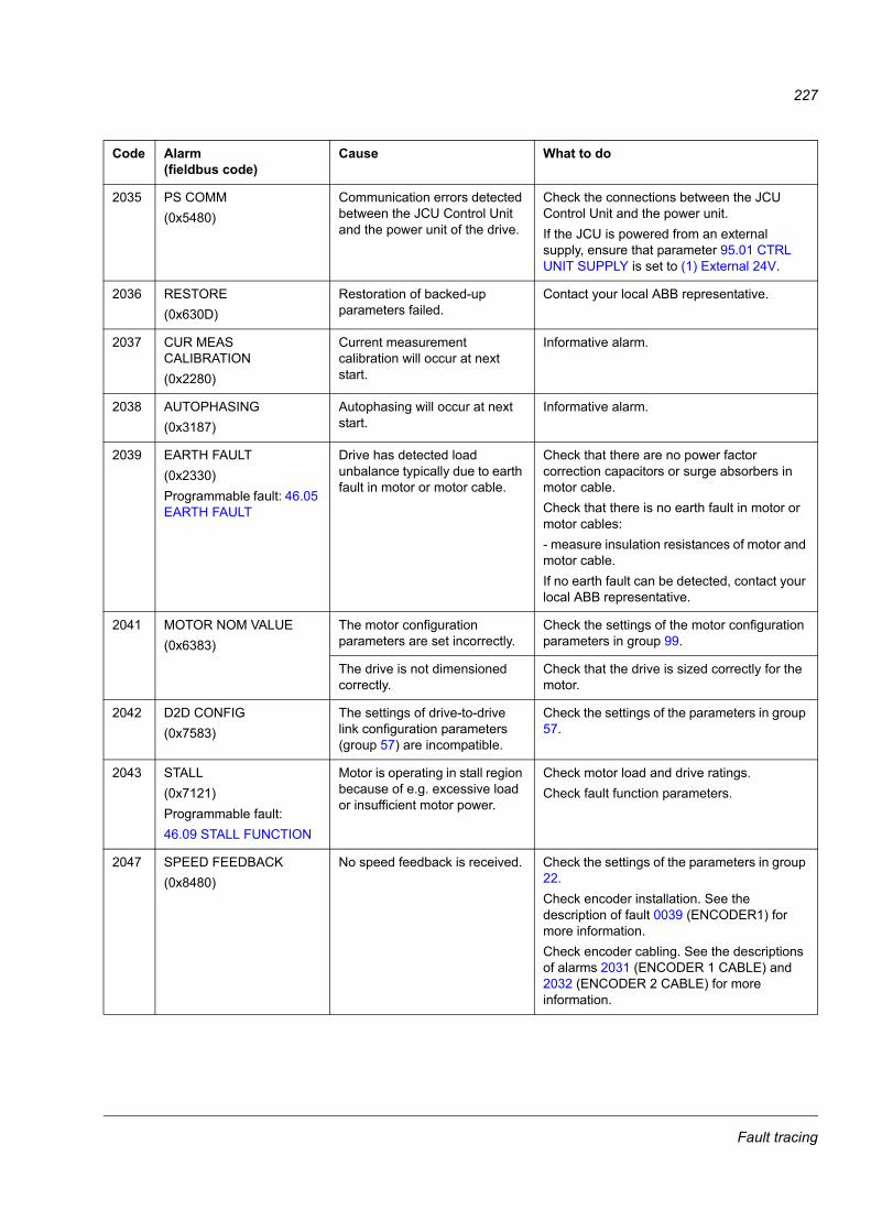
227
2035 PS COMM(0x5480)
Communication errors detected between the JCU Control Unit and the power unit of the drive.
Check the connections between the JCU Control Unit and the power unit.If the JCU is powered from an external supply, ensure that parameter 95.01 CTRL UNIT SUPPLY is set to (1) External 24V.
2036 RESTORE(0x630D)
Restoration of backed-up parameters failed.
Contact your local ABB representative.
2037 CUR MEAS CALIBRATION(0x2280)
Current measurement calibration will occur at next start.
Informative alarm.
2038 AUTOPHASING(0x3187)
Autophasing will occur at next start.
Informative alarm.
2039 EARTH FAULT(0x2330)Programmable fault: 46.05 EARTH FAULT
Drive has detected load unbalance typically due to earth fault in motor or motor cable.
Check that there are no power factor correction capacitors or surge absorbers in motor cable.Check that there is no earth fault in motor or motor cables:- measure insulation resistances of motor and motor cable.If no earth fault can be detected, contact your local ABB representative.
2041 MOTOR NOM VALUE(0x6383)
The motor configuration parameters are set incorrectly.
Check the settings of the motor configuration parameters in group 99.
The drive is not dimensioned correctly.
Check that the drive is sized correctly for the motor.
2042 D2D CONFIG(0x7583)
The settings of drive-to-drive link configuration parameters (group 57) are incompatible.
Check the settings of the parameters in group 57.
2043 STALL (0x7121)Programmable fault:46.09 STALL FUNCTION
Motor is operating in stall region because of e.g. excessive load or insufficient motor power.
Check motor load and drive ratings.Check fault function parameters.
2047 SPEED FEEDBACK(0x8480)
No speed feedback is received. Check the settings of the parameters in group 22.Check encoder installation. See the description of fault 0039 (ENCODER1) for more information.Check encoder cabling. See the descriptions of alarms 2031 (ENCODER 1 CABLE) and 2032 (ENCODER 2 CABLE) for more information.
Code Alarm(fieldbus code)
Cause What to do
Fault tracing
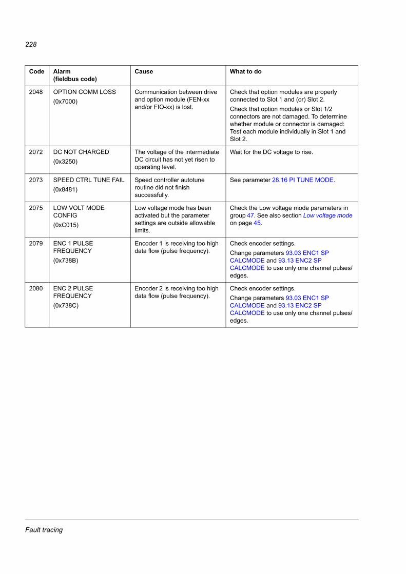
228
2048 OPTION COMM LOSS(0x7000)
Communication between drive and option module (FEN-xx and/or FIO-xx) is lost.
Check that option modules are properly connected to Slot 1 and (or) Slot 2.Check that option modules or Slot 1/2 connectors are not damaged. To determine whether module or connector is damaged: Test each module individually in Slot 1 and Slot 2.
2072 DC NOT CHARGED(0x3250)
The voltage of the intermediate DC circuit has not yet risen to operating level.
Wait for the DC voltage to rise.
2073 SPEED CTRL TUNE FAIL(0x8481)
Speed controller autotune routine did not finish successfully.
See parameter 28.16 PI TUNE MODE.
2075 LOW VOLT MODE CONFIG(0xC015)
Low voltage mode has been activated but the parameter settings are outside allowable limits.
Check the Low voltage mode parameters in group 47. See also section Low voltage mode on page 45.
2079 ENC 1 PULSE FREQUENCY(0x738B)
Encoder 1 is receiving too high data flow (pulse frequency).
Check encoder settings. Change parameters 93.03 ENC1 SP CALCMODE and 93.13 ENC2 SP CALCMODE to use only one channel pulses/edges.
2080 ENC 2 PULSE FREQUENCY(0x738C)
Encoder 2 is receiving too high data flow (pulse frequency).
Check encoder settings. Change parameters 93.03 ENC1 SP CALCMODE and 93.13 ENC2 SP CALCMODE to use only one channel pulses/edges.
Code Alarm(fieldbus code)
Cause What to do
Fault tracing
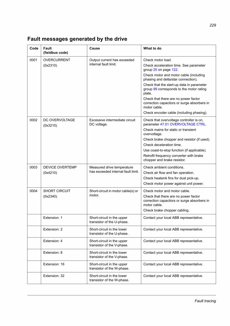
229
Fault messages generated by the driveCode Fault
(fieldbus code)Cause What to do
0001 OVERCURRENT(0x2310)
Output current has exceeded internal fault limit.
Check motor load.Check acceleration time. See parameter group 25 on page 122.Check motor and motor cable (including phasing and delta/star connection).Check that the start-up data in parameter group 99 corresponds to the motor rating plate.Check that there are no power factor correction capacitors or surge absorbers in motor cable.Check encoder cable (including phasing).
0002 DC OVERVOLTAGE(0x3210)
Excessive intermediate circuit DC voltage.
Check that overvoltage controller is on, parameter 47.01 OVERVOLTAGE CTRL.Check mains for static or transient overvoltage.Check brake chopper and resistor (if used).Check deceleration time.Use coast-to-stop function (if applicable).Retrofit frequency converter with brake chopper and brake resistor.
0003 DEVICE OVERTEMP(0x4210)
Measured drive temperature has exceeded internal fault limit.
Check ambient conditions.Check air flow and fan operation.Check heatsink fins for dust pick-up.Check motor power against unit power.
0004 SHORT CIRCUIT(0x2340)
Short-circuit in motor cable(s) or motor.
Check motor and motor cable.Check that there are no power factor correction capacitors or surge absorbers in motor cable.Check brake chopper cabling.
Extension: 1 Short-circuit in the upper transistor of the U-phase.
Contact your local ABB representative.
Extension: 2 Short-circuit in the lower transistor of the U-phase.
Contact your local ABB representative.
Extension: 4 Short-circuit in the upper transistor of the V-phase.
Contact your local ABB representative.
Extension: 8 Short-circuit in the lower transistor of the V-phase.
Contact your local ABB representative.
Extension: 16 Short-circuit in the upper transistor of the W-phase.
Contact your local ABB representative.
Extension: 32 Short-circuit in the lower transistor of the W-phase.
Contact your local ABB representative.
Fault tracing

230
0005 DC UNDERVOLTAGE(0x3220)
Intermediate circuit DC voltage is not sufficient due to missing mains phase, blown fuse or rectifier bridge internal fault.
Check mains supply and fuses.
0006 EARTH FAULT(0x2330)Programmable fault: 46.05 EARTH FAULT
Drive has detected load unbalance typically due to earth fault in motor or motor cable.
Check that there are no power factor correction capacitors or surge absorbers in motor cable.Check that there is no earth fault in motor or motor cables:- measure insulation resistances of motor and motor cable.If no earth fault can be detected, contact your local ABB representative.
0007 FAN FAULT(0xFF83)
Fan is not able to rotate freely or fan is disconnected. Fan operation is monitored by measuring fan current.
Check fan operation and connection.
0008 IGBT OVERTEMP(0x7184)
Drive temperature based on thermal model has exceeded internal fault limit.
Check ambient conditions.Check air flow and fan operation.Check heatsink fins for dust pick-up.Check motor power against unit power.
0009 BR SHORT CIRCUIT(0x7111)
Brake resistor short circuit or brake chopper control fault.
Check brake chopper and brake resistor connection.Ensure that brake resistor is not damaged.
0010 BR MISSING(0x7113)
Short circuit in brake chopper IGBT.
Ensure that brake resistor is connected and not damaged.
0011 BC OVERHEAT(0x7181)
Brake chopper IGBT temperature has exceeded internal fault limit.
Let chopper cool down.Check for excessive ambient temperature.Check for cooling fan failure.Check for obstructions in the air flow.Check the dimensioning and cooling of the cabinet.Check resistor overload protection function settings, parameters 48.03…48.05.Check that braking cycle meets allowed limits.Check that drive supply AC voltage is not excessive.
0012 BR OVERHEAT(0x7112)
Brake resistor temperature has exceeded fault limit defined by parameter 48.06 BR TEMP FAULTLIM.
Stop drive. Let resistor cool down. Check resistor overload protection function settings, parameters 48.01…48.05.Check fault limit setting, parameter 48.06.Check that braking cycle meets allowed limits.
Code Fault(fieldbus code)
Cause What to do
Fault tracing
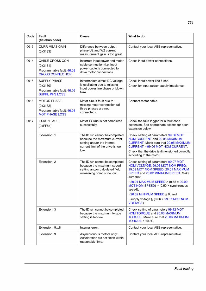
231
0013 CURR MEAS GAIN(0x3183)
Difference between output phase U2 and W2 current measurement gain is too great.
Contact your local ABB representative.
0014 CABLE CROSS CON(0x3181)Programmable fault: 46.08 CROSS CONNECTION
Incorrect input power and motor cable connection (i.e. input power cable is connected to drive motor connection).
Check input power connections.
0015 SUPPLY PHASE(0x3130)Programmable fault: 46.06 SUPPL PHS LOSS
Intermediate circuit DC voltage is oscillating due to missing input power line phase or blown fuse.
Check input power line fuses.Check for input power supply imbalance.
0016 MOTOR PHASE(0x3182)Programmable fault: 46.04 MOT PHASE LOSS
Motor circuit fault due to missing motor connection (all three phases are not connected).
Connect motor cable.
0017 ID-RUN FAULT(0xFF84)
Motor ID Run is not completed successfully.
Check the fault logger for a fault code extension. See appropriate actions for each extension below.
Extension: 1 The ID run cannot be completed because the maximum current setting and/or the internal current limit of the drive is too low.
Check setting of parameters 99.06 MOT NOM CURRENT and 20.05 MAXIMUM CURRENT. Make sure that 20.05 MAXIMUM CURRENT > 99.06 MOT NOM CURRENT.Check that the drive is dimensioned correctly according to the motor.
Extension: 2 The ID run cannot be completed because the maximum speed setting and/or calculated field weakening point is too low.
Check setting of parameters 99.07 MOT NOM VOLTAGE, 99.08 MOT NOM FREQ, 99.09 MOT NOM SPEED, 20.01 MAXIMUM SPEED and 20.02 MINIMUM SPEED. Make sure that• 20.01 MAXIMUM SPEED > (0.55 × 99.09 MOT NOM SPEED) > (0.50 × synchronous speed),• 20.02 MINIMUM SPEED < 0, and• supply voltage > (0.66 × 99.07 MOT NOM VOLTAGE).
Extension: 3 The ID run cannot be completed because the maximum torque setting is too low.
Check setting of parameters 99.12 MOT NOM TORQUE and 20.06 MAXIMUM TORQUE. Make sure that 20.06 MAXIMUM TORQUE > 100%.
Extension: 5…8 Internal error. Contact your local ABB representative.
Extension: 9 Asynchronous motors only: Acceleration did not finish within reasonable time.
Contact your local ABB representative.
Code Fault(fieldbus code)
Cause What to do
Fault tracing

232
Extension: 10 Asynchronous motors only: Deceleration did not finish within reasonable time.
Contact your local ABB representative.
Extension: 11 Asynchronous motors only: Speed dropped to zero during ID run.
Contact your local ABB representative.
Extension: 12 Permanent magnet motors only: First acceleration did not finish within reasonable time.
Contact your local ABB representative.
Extension: 13 Permanent magnet motors only: Second acceleration did not finish within reasonable time.
Contact your local ABB representative.
Extension: 14…16 Internal error. Contact your local ABB representative.
0018 CURR U2 MEAS(0x3184)
Measured offset error of U2 output phase current measurement is too great. (Offset value is updated during current calibration.)
Contact your local ABB representative.
0019 CURR V2 MEAS(0x3185)
Measured offset error of V2 output phase current measurement is too great. (Offset value is updated during current calibration.)
Contact your local ABB representative.
0020 CURR W2 MEAS(0x3186)
Measured offset error of W2 output phase current measurement is too great. (Offset value is updated during current calibration.)
Contact your local ABB representative.
0021 STO1 LOST(0x8182)
Safe Torque Off function is active, i.e. safety circuit signal 1 connected between X6:1 and X6:3 is lost while drive is at stopped state and parameter 46.07 STO DIAGNOSTIC setting is (2) Alarm or (3) No.
Check safety circuit connections. For more information, see the appropriate drive hardware manual and Application guide - Safe torque off function for ACSM1, ACS850 and ACQ810 drives (3AFE68929814 [English]).
0022 STO2 LOST(0x8183)
Safe Torque Off function is active, i.e. safety circuit signal 2 connected between X6:2 and X6:4 is lost while drive is at stopped state and parameter 46.07 STO DIAGNOSTIC setting is (2) Alarm or (3) No.
Check safety circuit connections. For more information, see the appropriate drive hardware manual and Application guide - Safe torque off function for ACSM1, ACS850 and ACQ810 drives (3AFE68929814 [English]).
Code Fault(fieldbus code)
Cause What to do
Fault tracing
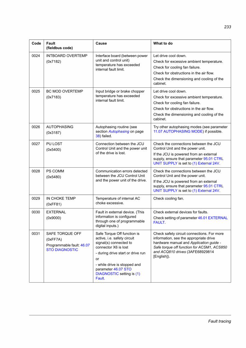
233
0024 INTBOARD OVERTEMP(0x7182)
Interface board (between power unit and control unit) temperature has exceeded internal fault limit.
Let drive cool down.Check for excessive ambient temperature.Check for cooling fan failure.Check for obstructions in the air flow.Check the dimensioning and cooling of the cabinet.
0025 BC MOD OVERTEMP(0x7183)
Input bridge or brake chopper temperature has exceeded internal fault limit.
Let drive cool down.Check for excessive ambient temperature.Check for cooling fan failure.Check for obstructions in the air flow.Check the dimensioning and cooling of the cabinet.
0026 AUTOPHASING(0x3187)
Autophasing routine (see section Autophasing on page 38) failed.
Try other autophasing modes (see parameter 11.07 AUTOPHASING MODE) if possible.
0027 PU LOST(0x5400)
Connection between the JCU Control Unit and the power unit of the drive is lost.
Check the connections between the JCU Control Unit and the power unit.If the JCU is powered from an external supply, ensure that parameter 95.01 CTRL UNIT SUPPLY is set to (1) External 24V.
0028 PS COMM(0x5480)
Communication errors detected between the JCU Control Unit and the power unit of the drive.
Check the connections between the JCU Control Unit and the power unit.If the JCU is powered from an external supply, ensure that parameter 95.01 CTRL UNIT SUPPLY is set to (1) External 24V.
0029 IN CHOKE TEMP(0xFF81)
Temperature of internal AC choke excessive.
Check cooling fan.
0030 EXTERNAL(0x9000)
Fault in external device. (This information is configured through one of programmable digital inputs.)
Check external devices for faults.Check setting of parameter 46.01 EXTERNAL FAULT.
0031 SAFE TORQUE OFF(0xFF7A)Programmable fault: 46.07 STO DIAGNOSTIC
Safe Torque Off function is active, i.e. safety circuit signal(s) connected to connector X6 is lost - during drive start or drive run or- while drive is stopped and parameter 46.07 STO DIAGNOSTIC setting is (1) Fault.
Check safety circuit connections. For more information, see the appropriate drive hardware manual and Application guide - Safe torque off function for ACSM1, ACS850 and ACQ810 drives (3AFE68929814 [English]).
Code Fault(fieldbus code)
Cause What to do
Fault tracing

234
0032 OVERSPEED(0x7310)
Motor is turning faster than highest allowed speed due to incorrectly set minimum/maximum speed, insufficient braking torque or changes in load when using torque reference.
Check minimum/maximum speed settings, parameters 20.01 MAXIMUM SPEED and 20.02 MINIMUM SPEED.Check adequacy of motor braking torque.Check applicability of torque control.Check need for brake chopper and resistor(s).
0033 BRAKE START TORQUE(0x7185)Programmable fault: 35.09 BRAKE FAULT FUNC
Mechanical brake fault. Fault is activated if required motor starting torque, 35.06 BRAKE OPEN TORQ, is not achieved.
Check brake open torque setting, parameter 35.06.Check drive torque and current limits. See parameter group 20 on page 108.
0034 BRAKE NOT CLOSED(0x7186)Programmable fault: 35.09 BRAKE FAULT FUNC
Mechanical brake control fault. Fault is activated if brake acknowledgement is not as expected during brake closing.
Check mechanical brake connection.Check mechanical brake settings, parameters 35.01…35.09.To determine whether problem is with acknowledgement signal or brake: Check if brake is closed or open.
0035 BRAKE NOT OPEN(0x7187)Programmable fault: 35.09 BRAKE FAULT FUNC
Mechanical brake control fault. Fault is activated if brake acknowledgement is not as expected during brake opening.
Check mechanical brake connection.Check mechanical brake settings, parameters 35.01…35.08.To determine whether problem is with acknowledgement signal or brake: Check if brake is closed or open.
0036 LOCAL CTRL LOSS(0x5300)Programmable fault: 46.03 LOCAL CTRL LOSS
Control panel or PC tool selected as active control location for drive has ceased communicating.
Check PC tool or control panel connection.Check control panel connector.Replace control panel in mounting platform.
0037 NVMEMCORRUPTED(0x6320)
Drive internal faultNote: This fault cannot be reset.
Check the fault logger for a fault code extension. See appropriate actions for each extension below.
Fault code extension: 2051 Total number of parameters (including unused space between parameters) exceeds firmware maximum.
Move parameters from the firmware groups to the application groups.Reduce the number of parameters.
Fault code extension: Other
Drive internal fault. Contact your local ABB representative.
0038 OPTION COMM LOSS(0x7000)
Communication between drive and option module (FEN-xx and/or FIO-xx) is lost.
Check that option modules are properly connected to Slot 1 and (or) Slot 2.Check that option modules or Slot 1/2 connectors are not damaged. To determine whether module or connector is damaged: Test each module individually in Slot 1 and Slot 2.
Code Fault(fieldbus code)
Cause What to do
Fault tracing
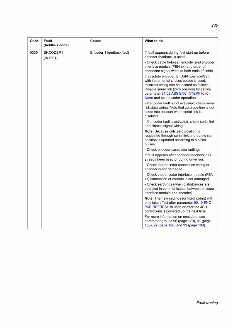
235
0039 ENCODER1(0x7301)
Encoder 1 feedback fault If fault appears during first start-up before encoder feedback is used:- Check cable between encoder and encoder interface module (FEN-xx) and order of connector signal wires at both ends of cable.If absolute encoder, EnDat/Hiperface/SSI, with incremental sin/cos pulses is used, incorrect wiring can be located as follows: Disable serial link (zero position) by setting parameter 91.02 ABS ENC INTERF to (0) None and test encoder operation:- If encoder fault is not activated, check serial link data wiring. Note that zero position is not taken into account when serial link is disabled.- If encoder fault is activated, check serial link and sin/cos signal wiring.Note: Because only zero position is requested through serial link and during run, position is updated according to sin/cos pulses. - Check encoder parameter settings.If fault appears after encoder feedback has already been used or during drive run:- Check that encoder connection wiring or encoder is not damaged. - Check that encoder interface module (FEN-xx) connection or module is not damaged. - Check earthings (when disturbances are detected in communication between encoder interface module and encoder).Note: The new settings (or fixed wiring) will only take effect after parameter 90.10 ENC PAR REFRESH is used or after the JCU control unit is powered up the next time.For more information on encoders, see parameter groups 90 (page 179), 91 (page 183), 92 (page 188) and 93 (page 189).
Code Fault(fieldbus code)
Cause What to do
Fault tracing
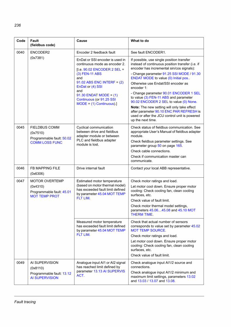
236
0040 ENCODER2(0x7381)
Encoder 2 feedback fault See fault ENCODER1.
EnDat or SSI encoder is used in continuous mode as encoder 2. [I.e. 90.02 ENCODER 2 SEL = (3) FEN-11 ABSand91.02 ABS ENC INTERF = (2) EnDat or (4) SSIand91.30 ENDAT MODE = (1) Continuous (or 91.25 SSI MODE = (1) Continuous).]
If possible, use single position transfer instead of continuous position transfer (i.e. if encoder has incremental sin/cos signals):- Change parameter 91.25 SSI MODE / 91.30 ENDAT MODE to value (0) Initial pos..Otherwise use Endat/SSI encoder as encoder 1:- Change parameter 90.01 ENCODER 1 SEL to value (3) FEN-11 ABS and parameter 90.02 ENCODER 2 SEL to value (0) None.Note: The new setting will only take effect after parameter 90.10 ENC PAR REFRESH is used or after the JCU control unit is powered up the next time.
0045 FIELDBUS COMM(0x7510)Programmable fault: 50.02 COMM LOSS FUNC
Cyclical communication between drive and fieldbus adapter module or between PLC and fieldbus adapter module is lost.
Check status of fieldbus communication. See appropriate User’s Manual of fieldbus adapter module.Check fieldbus parameter settings. See parameter group 50 on page 165.Check cable connections.Check if communication master can communicate.
0046 FB MAPPING FILE(0x6306)
Drive internal fault Contact your local ABB representative.
0047 MOTOR OVERTEMP(0x4310)Programmable fault: 45.01 MOT TEMP PROT
Estimated motor temperature (based on motor thermal model) has exceeded fault limit defined by parameter 45.04 MOT TEMP FLT LIM.
Check motor ratings and load.Let motor cool down. Ensure proper motor cooling: Check cooling fan, clean cooling surfaces, etc.Check value of fault limit.Check motor thermal model settings, parameters 45.06…45.08 and 45.10 MOT THERM TIME.
Measured motor temperature has exceeded fault limit defined by parameter 45.04 MOT TEMP FLT LIM.
Check that actual number of sensors corresponds to value set by parameter 45.02 MOT TEMP SOURCE.Check motor ratings and load.Let motor cool down. Ensure proper motor cooling: Check cooling fan, clean cooling surfaces, etc.Check value of fault limit.
0049 AI SUPERVISION(0x8110)Programmable fault: 13.12 AI SUPERVISION
Analogue input AI1 or AI2 signal has reached limit defined by parameter 13.13 AI SUPERVIS ACT.
Check analogue input AI1/2 source and connections. Check analogue input AI1/2 minimum and maximum limit settings, parameters 13.02 and 13.03 / 13.07 and 13.08.
Code Fault(fieldbus code)
Cause What to do
Fault tracing
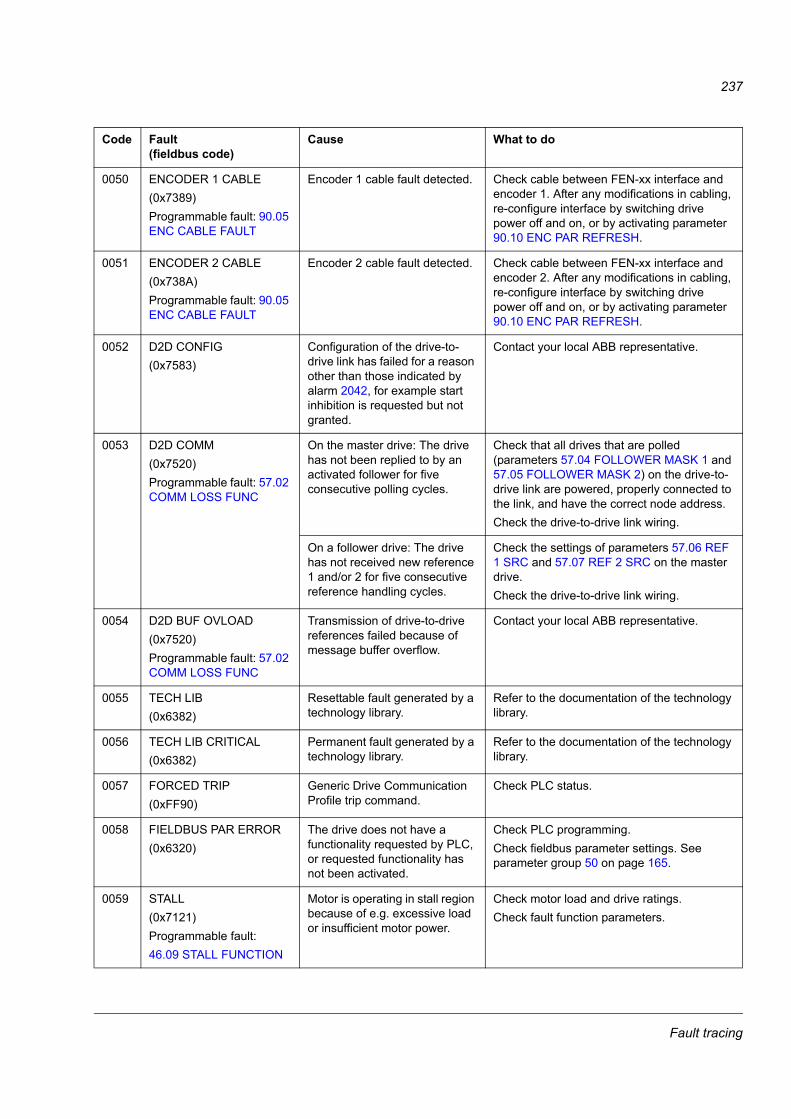
237
0050 ENCODER 1 CABLE(0x7389)Programmable fault: 90.05 ENC CABLE FAULT
Encoder 1 cable fault detected. Check cable between FEN-xx interface and encoder 1. After any modifications in cabling, re-configure interface by switching drive power off and on, or by activating parameter 90.10 ENC PAR REFRESH.
0051 ENCODER 2 CABLE(0x738A)Programmable fault: 90.05 ENC CABLE FAULT
Encoder 2 cable fault detected. Check cable between FEN-xx interface and encoder 2. After any modifications in cabling, re-configure interface by switching drive power off and on, or by activating parameter 90.10 ENC PAR REFRESH.
0052 D2D CONFIG(0x7583)
Configuration of the drive-to-drive link has failed for a reason other than those indicated by alarm 2042, for example start inhibition is requested but not granted.
Contact your local ABB representative.
0053 D2D COMM(0x7520)Programmable fault: 57.02 COMM LOSS FUNC
On the master drive: The drive has not been replied to by an activated follower for five consecutive polling cycles.
Check that all drives that are polled (parameters 57.04 FOLLOWER MASK 1 and 57.05 FOLLOWER MASK 2) on the drive-to-drive link are powered, properly connected to the link, and have the correct node address.Check the drive-to-drive link wiring.
On a follower drive: The drive has not received new reference 1 and/or 2 for five consecutive reference handling cycles.
Check the settings of parameters 57.06 REF 1 SRC and 57.07 REF 2 SRC on the master drive.Check the drive-to-drive link wiring.
0054 D2D BUF OVLOAD(0x7520)Programmable fault: 57.02 COMM LOSS FUNC
Transmission of drive-to-drive references failed because of message buffer overflow.
Contact your local ABB representative.
0055 TECH LIB(0x6382)
Resettable fault generated by a technology library.
Refer to the documentation of the technology library.
0056 TECH LIB CRITICAL(0x6382)
Permanent fault generated by a technology library.
Refer to the documentation of the technology library.
0057 FORCED TRIP(0xFF90)
Generic Drive Communication Profile trip command.
Check PLC status.
0058 FIELDBUS PAR ERROR(0x6320)
The drive does not have a functionality requested by PLC, or requested functionality has not been activated.
Check PLC programming.Check fieldbus parameter settings. See parameter group 50 on page 165.
0059 STALL (0x7121)Programmable fault:46.09 STALL FUNCTION
Motor is operating in stall region because of e.g. excessive load or insufficient motor power.
Check motor load and drive ratings.Check fault function parameters.
Code Fault(fieldbus code)
Cause What to do
Fault tracing

238
0061 SPEED FEEDBACK(0x8480)
No speed feedback is received. Check the settings of the parameters in group 22.Check encoder installation. See the description of fault 0039 (ENCODER1) for more information.Check encoder cabling. See the descriptions of faults 0050 (ENCODER1) and 0051 (ENCODER2) for more information.
0062 D2D SLOT COMM(0x7584)
Drive-to-drive link is set to use an FMBA module for communication, but no module is detected in specified slot.
Check the settings of parameters 57.01 LINK MODE and 57.15 D2D COMM PORT. Ensure that the FMBA module has been detected by checking parameters 9.20…9.22.Check that the FMBA module is correctly wired.Try installing the FMBA module into another slot. If the problem persists, contact your local ABB representative.
0067 FPGA ERROR1(0x5401)
Drive internal fault Contact your local ABB representative.
0068 FPGA ERROR2(0x5402)
Drive internal fault Contact your local ABB representative.
0069 ADC ERROR(0x5403)
Drive internal fault Contact your local ABB representative.
0073 ENC 1 PULSE FREQUENCY(0x738B)
Encoder 1 is receiving too high data flow (pulse frequency).
Check encoder settings. Change parameters 93.03 ENC1 SP CALCMODE and 93.13 ENC2 SP CALCMODE to use only one channel pulses/edges.
0074 ENC 2 PULSE FREQUENCY (0x738C)
Encoder 2 is receiving too high data flow (pulse frequency).
Check encoder settings. Change parameters 93.03 ENC1 SP CALCMODE and 93.13 ENC2 SP CALCMODE to use only one channel pulses/edges.
0201 T2 OVERLOAD(0x0201)
Firmware time level 2 overloadNote: This fault cannot be reset.
Contact your local ABB representative.
0202 T3 OVERLOAD(0x6100)
Firmware time level 3 overloadNote: This fault cannot be reset.
Contact your local ABB representative.
0203 T4 OVERLOAD(0x6100)
Firmware time level 4 overloadNote: This fault cannot be reset.
Contact your local ABB representative.
Code Fault(fieldbus code)
Cause What to do
Fault tracing
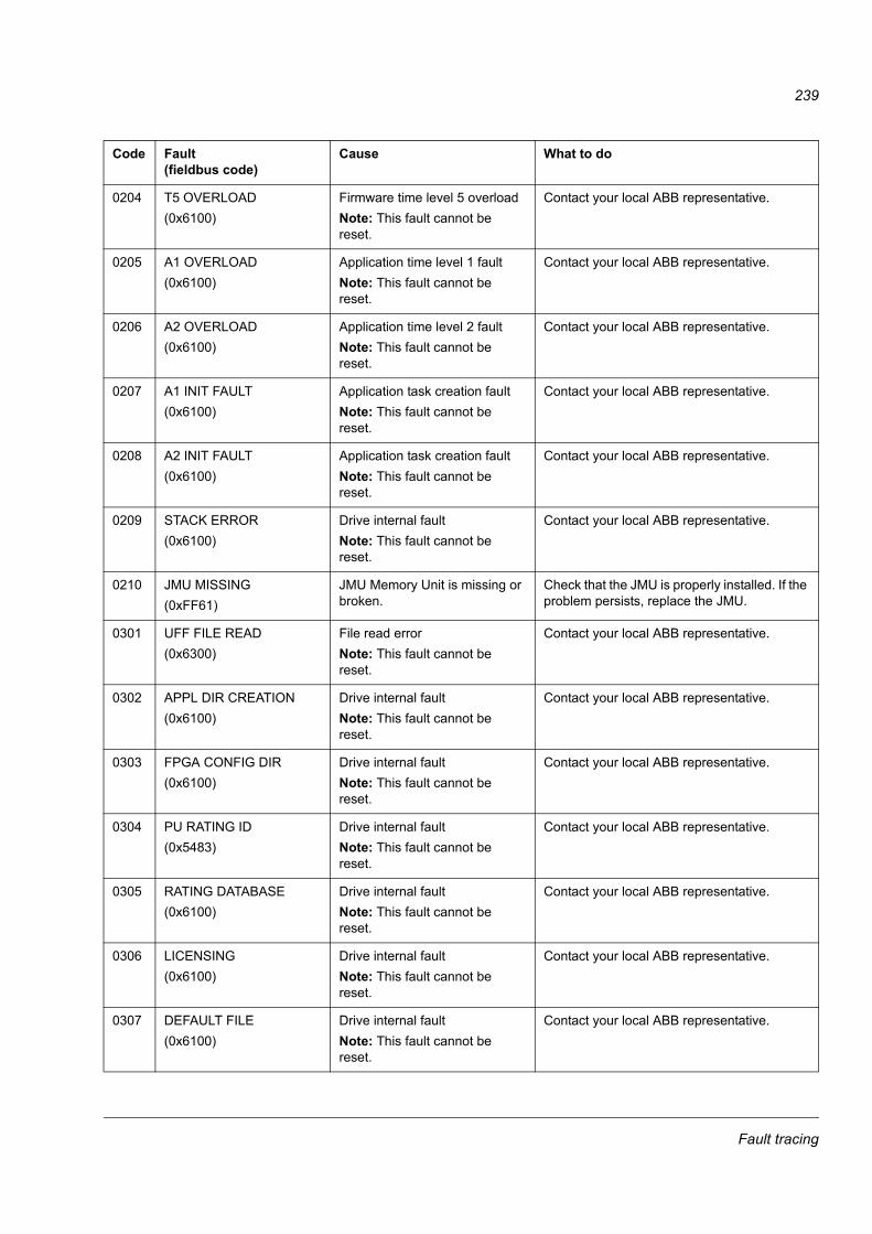
239
0204 T5 OVERLOAD(0x6100)
Firmware time level 5 overloadNote: This fault cannot be reset.
Contact your local ABB representative.
0205 A1 OVERLOAD(0x6100)
Application time level 1 faultNote: This fault cannot be reset.
Contact your local ABB representative.
0206 A2 OVERLOAD(0x6100)
Application time level 2 faultNote: This fault cannot be reset.
Contact your local ABB representative.
0207 A1 INIT FAULT(0x6100)
Application task creation faultNote: This fault cannot be reset.
Contact your local ABB representative.
0208 A2 INIT FAULT(0x6100)
Application task creation faultNote: This fault cannot be reset.
Contact your local ABB representative.
0209 STACK ERROR(0x6100)
Drive internal faultNote: This fault cannot be reset.
Contact your local ABB representative.
0210 JMU MISSING(0xFF61)
JMU Memory Unit is missing or broken.
Check that the JMU is properly installed. If the problem persists, replace the JMU.
0301 UFF FILE READ(0x6300)
File read errorNote: This fault cannot be reset.
Contact your local ABB representative.
0302 APPL DIR CREATION(0x6100)
Drive internal faultNote: This fault cannot be reset.
Contact your local ABB representative.
0303 FPGA CONFIG DIR(0x6100)
Drive internal faultNote: This fault cannot be reset.
Contact your local ABB representative.
0304 PU RATING ID(0x5483)
Drive internal faultNote: This fault cannot be reset.
Contact your local ABB representative.
0305 RATING DATABASE(0x6100)
Drive internal faultNote: This fault cannot be reset.
Contact your local ABB representative.
0306 LICENSING(0x6100)
Drive internal faultNote: This fault cannot be reset.
Contact your local ABB representative.
0307 DEFAULT FILE(0x6100)
Drive internal faultNote: This fault cannot be reset.
Contact your local ABB representative.
Code Fault(fieldbus code)
Cause What to do
Fault tracing

240
0308 APPL FILE PAR CONF (0x6300)
Corrupted application fileNote: This fault cannot be reset.
Reload application.If fault is still active, contact your local ABB representative.
0309 APPL LOADING(0x6300)
Application file incompatible or corrupted.Note: This fault cannot be reset.
Check the fault logger for a fault code extension. See appropriate actions for each extension below.
Fault code extension: 8 Template used in the application incompatible with drive firmware.
Change the template of the application in DriveSPC.
Fault code extension: 10 Parameters defined in the application conflict with existing drive parameters.
Check the application for conflicting parameters.
Fault code extension: 35 Application memory full. Contact your local ABB representative.
Fault code extension: Other
Corrupted application file Reload application.If fault is still active, contact your local ABB representative.
0310 USERSET LOAD(0xFF69)
Loading of user set is not successfully completed because:- requested user set does not exist- user set is not compatible with drive program- drive has been switched off during loading.
Reload.
0311 USERSET SAVE(0xFF69)
User set is not saved because of memory corruption.
Check the setting of parameter 95.01 CTRL UNIT SUPPLY.If the fault still occurs, contact your local ABB representative.
0312 UFF OVERSIZE(0x6300)
UFF file is too big. Contact your local ABB representative.
0313 UFF EOF(0x6300)
UFF file structure failure Contact your local ABB representative.
0314 TECH LIB INTERFACE(0x6100)
Incompatible firmware interfaceNote: This fault cannot be reset.
Contact your local ABB representative.
0315 RESTORE FILE(0x630D)
Restoration of backed-up parameters failed.
Contact your local ABB representative.The fault is reset after a successful restoration via the control panel or DriveStudio.
Code Fault(fieldbus code)
Cause What to do
Fault tracing
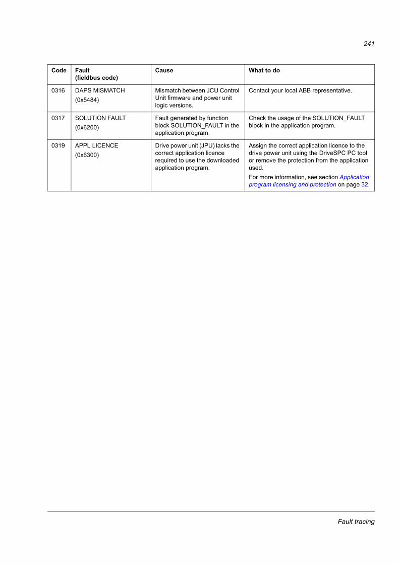
241
0316 DAPS MISMATCH(0x5484)
Mismatch between JCU Control Unit firmware and power unit logic versions.
Contact your local ABB representative.
0317 SOLUTION FAULT(0x6200)
Fault generated by function block SOLUTION_FAULT in the application program.
Check the usage of the SOLUTION_FAULT block in the application program.
0319 APPL LICENCE(0x6300)
Drive power unit (JPU) lacks the correct application licence required to use the downloaded application program.
Assign the correct application licence to the drive power unit using the DriveSPC PC tool or remove the protection from the application used. For more information, see section Application program licensing and protection on page 32.
Code Fault(fieldbus code)
Cause What to do
Fault tracing

242
Fault tracing
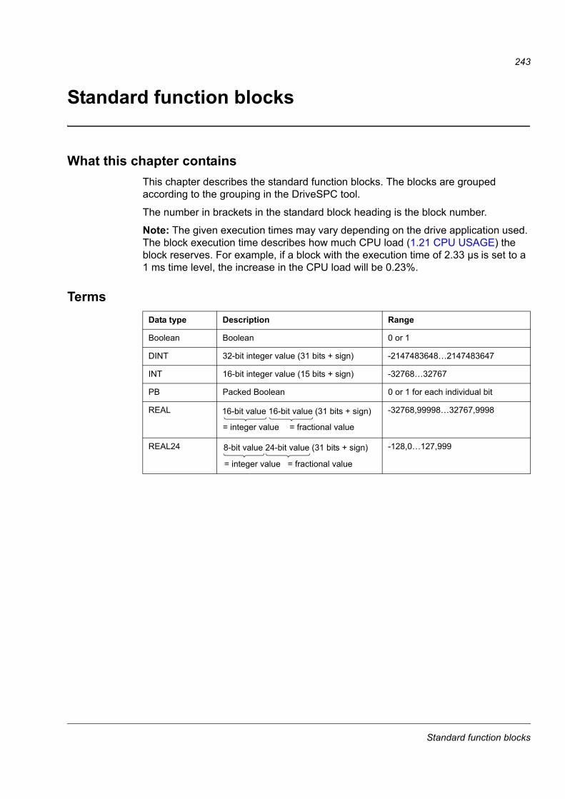
243
Standard function blocks
What this chapter containsThis chapter describes the standard function blocks. The blocks are grouped according to the grouping in the DriveSPC tool.
The number in brackets in the standard block heading is the block number.
Note: The given execution times may vary depending on the drive application used. The block execution time describes how much CPU load (1.21 CPU USAGE) the block reserves. For example, if a block with the execution time of 2.33 µs is set to a 1 ms time level, the increase in the CPU load will be 0.23%.
TermsData type Description Range
Boolean Boolean 0 or 1
DINT 32-bit integer value (31 bits + sign) -2147483648…2147483647
INT 16-bit integer value (15 bits + sign) -32768…32767
PB Packed Boolean 0 or 1 for each individual bit
REAL -32768,99998…32767,9998
REAL24 -128,0…127,999
16-bit value 16-bit value (31 bits + sign)
= integer value = fractional value
8-bit value 24-bit value (31 bits + sign)
= integer value = fractional value
Standard function blocks
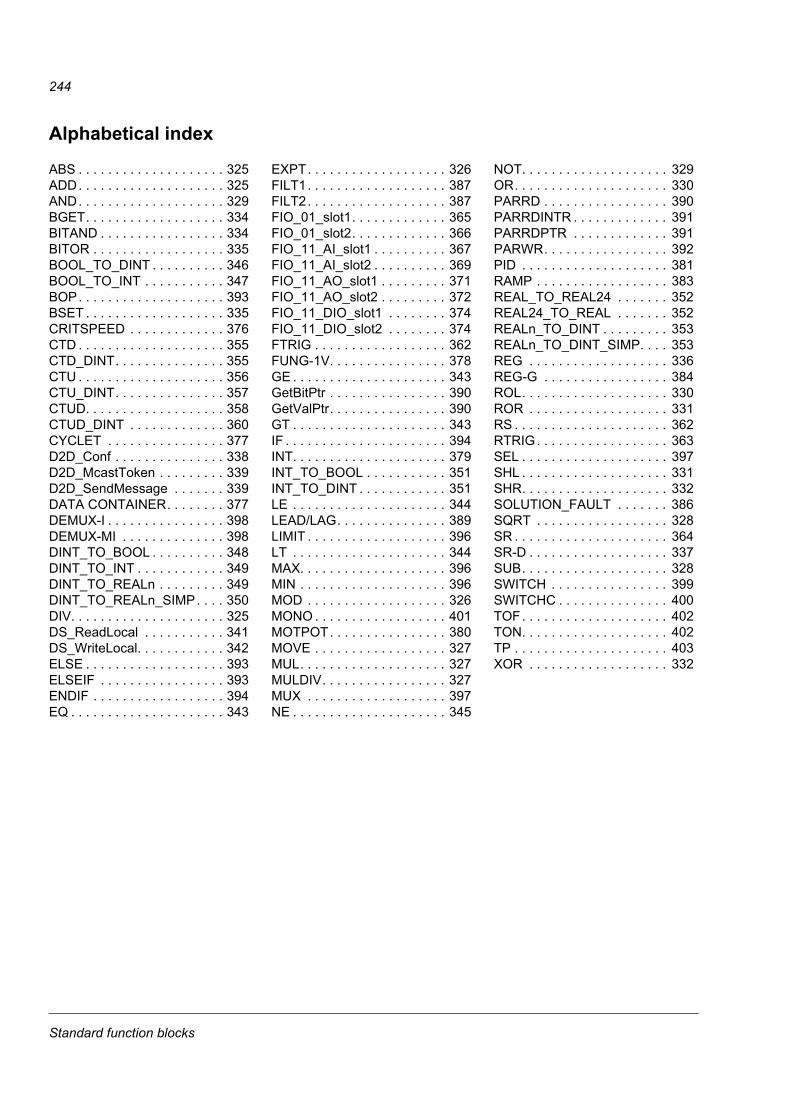
244
Alphabetical index
ABS . . . . . . . . . . . . . . . . . . . . 325ADD. . . . . . . . . . . . . . . . . . . . 325AND. . . . . . . . . . . . . . . . . . . . 329BGET. . . . . . . . . . . . . . . . . . . 334BITAND . . . . . . . . . . . . . . . . . 334BITOR . . . . . . . . . . . . . . . . . . 335BOOL_TO_DINT . . . . . . . . . . 346BOOL_TO_INT . . . . . . . . . . . 347BOP. . . . . . . . . . . . . . . . . . . . 393BSET . . . . . . . . . . . . . . . . . . . 335CRITSPEED . . . . . . . . . . . . . 376CTD . . . . . . . . . . . . . . . . . . . . 355CTD_DINT. . . . . . . . . . . . . . . 355CTU . . . . . . . . . . . . . . . . . . . . 356CTU_DINT. . . . . . . . . . . . . . . 357CTUD. . . . . . . . . . . . . . . . . . . 358CTUD_DINT . . . . . . . . . . . . . 360CYCLET . . . . . . . . . . . . . . . . 377D2D_Conf . . . . . . . . . . . . . . . 338D2D_McastToken . . . . . . . . . 339D2D_SendMessage . . . . . . . 339DATA CONTAINER. . . . . . . . 377DEMUX-I . . . . . . . . . . . . . . . . 398DEMUX-MI . . . . . . . . . . . . . . 398DINT_TO_BOOL . . . . . . . . . . 348DINT_TO_INT . . . . . . . . . . . . 349DINT_TO_REALn . . . . . . . . . 349DINT_TO_REALn_SIMP. . . . 350DIV. . . . . . . . . . . . . . . . . . . . . 325DS_ReadLocal . . . . . . . . . . . 341DS_WriteLocal. . . . . . . . . . . . 342ELSE . . . . . . . . . . . . . . . . . . . 393ELSEIF . . . . . . . . . . . . . . . . . 393ENDIF . . . . . . . . . . . . . . . . . . 394EQ . . . . . . . . . . . . . . . . . . . . . 343
EXPT. . . . . . . . . . . . . . . . . . . 326FILT1. . . . . . . . . . . . . . . . . . . 387FILT2. . . . . . . . . . . . . . . . . . . 387FIO_01_slot1. . . . . . . . . . . . . 365FIO_01_slot2. . . . . . . . . . . . . 366FIO_11_AI_slot1 . . . . . . . . . . 367FIO_11_AI_slot2 . . . . . . . . . . 369FIO_11_AO_slot1 . . . . . . . . . 371FIO_11_AO_slot2 . . . . . . . . . 372FIO_11_DIO_slot1 . . . . . . . . 374FIO_11_DIO_slot2 . . . . . . . . 374FTRIG . . . . . . . . . . . . . . . . . . 362FUNG-1V. . . . . . . . . . . . . . . . 378GE . . . . . . . . . . . . . . . . . . . . . 343GetBitPtr . . . . . . . . . . . . . . . . 390GetValPtr. . . . . . . . . . . . . . . . 390GT . . . . . . . . . . . . . . . . . . . . . 343IF . . . . . . . . . . . . . . . . . . . . . . 394INT. . . . . . . . . . . . . . . . . . . . . 379INT_TO_BOOL . . . . . . . . . . . 351INT_TO_DINT . . . . . . . . . . . . 351LE . . . . . . . . . . . . . . . . . . . . . 344LEAD/LAG. . . . . . . . . . . . . . . 389LIMIT . . . . . . . . . . . . . . . . . . . 396LT . . . . . . . . . . . . . . . . . . . . . 344MAX. . . . . . . . . . . . . . . . . . . . 396MIN . . . . . . . . . . . . . . . . . . . . 396MOD . . . . . . . . . . . . . . . . . . . 326MONO . . . . . . . . . . . . . . . . . . 401MOTPOT. . . . . . . . . . . . . . . . 380MOVE . . . . . . . . . . . . . . . . . . 327MUL. . . . . . . . . . . . . . . . . . . . 327MULDIV. . . . . . . . . . . . . . . . . 327MUX . . . . . . . . . . . . . . . . . . . 397NE . . . . . . . . . . . . . . . . . . . . . 345
NOT. . . . . . . . . . . . . . . . . . . . 329OR. . . . . . . . . . . . . . . . . . . . . 330PARRD . . . . . . . . . . . . . . . . . 390PARRDINTR . . . . . . . . . . . . . 391PARRDPTR . . . . . . . . . . . . . 391PARWR. . . . . . . . . . . . . . . . . 392PID . . . . . . . . . . . . . . . . . . . . 381RAMP . . . . . . . . . . . . . . . . . . 383REAL_TO_REAL24 . . . . . . . 352REAL24_TO_REAL . . . . . . . 352REALn_TO_DINT . . . . . . . . . 353REALn_TO_DINT_SIMP. . . . 353REG . . . . . . . . . . . . . . . . . . . 336REG-G . . . . . . . . . . . . . . . . . 384ROL. . . . . . . . . . . . . . . . . . . . 330ROR . . . . . . . . . . . . . . . . . . . 331RS . . . . . . . . . . . . . . . . . . . . . 362RTRIG. . . . . . . . . . . . . . . . . . 363SEL . . . . . . . . . . . . . . . . . . . . 397SHL . . . . . . . . . . . . . . . . . . . . 331SHR. . . . . . . . . . . . . . . . . . . . 332SOLUTION_FAULT . . . . . . . 386SQRT . . . . . . . . . . . . . . . . . . 328SR . . . . . . . . . . . . . . . . . . . . . 364SR-D . . . . . . . . . . . . . . . . . . . 337SUB. . . . . . . . . . . . . . . . . . . . 328SWITCH . . . . . . . . . . . . . . . . 399SWITCHC . . . . . . . . . . . . . . . 400TOF. . . . . . . . . . . . . . . . . . . . 402TON. . . . . . . . . . . . . . . . . . . . 402TP . . . . . . . . . . . . . . . . . . . . . 403XOR . . . . . . . . . . . . . . . . . . . 332
Standard function blocks
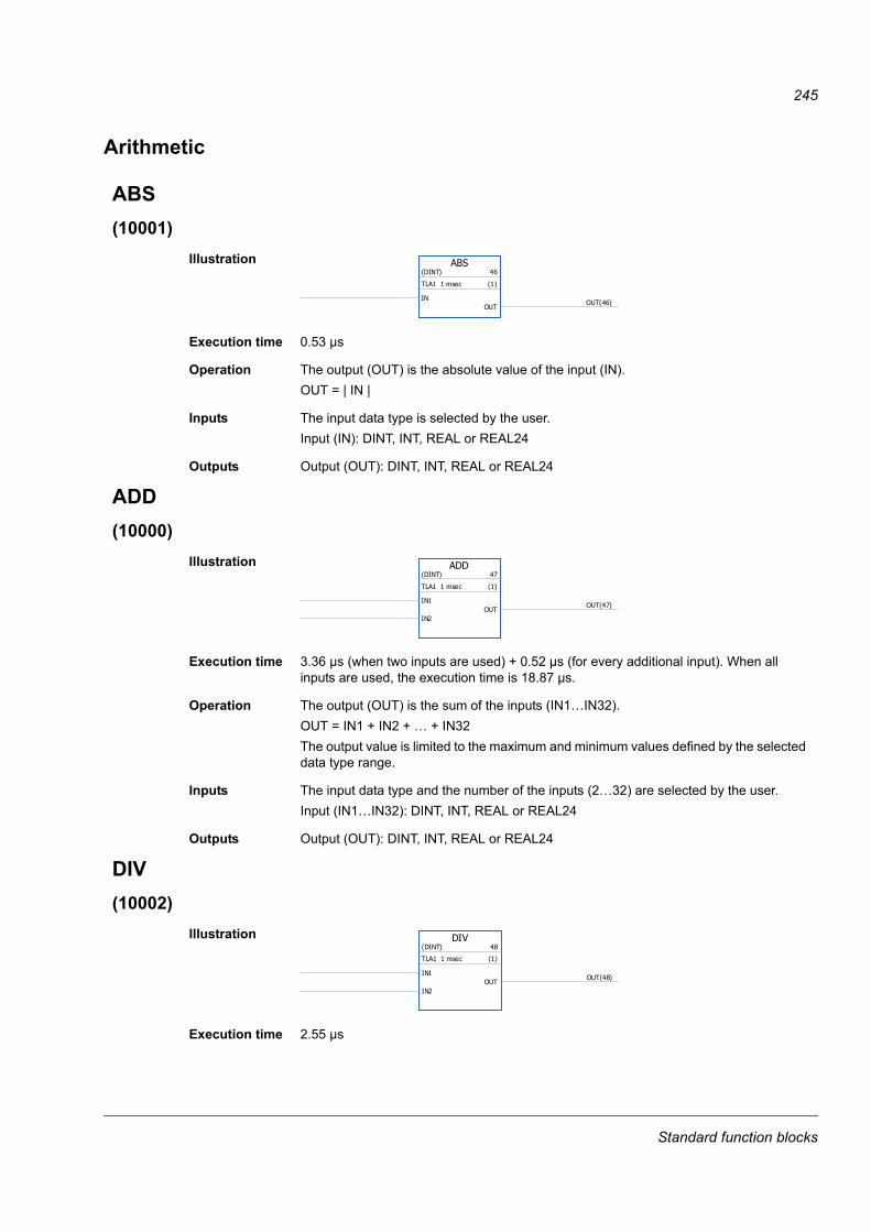
245
Arithmetic
ABS(10001)
Illustration
Execution time 0.53 µs
Operation The output (OUT) is the absolute value of the input (IN).OUT = | IN |
Inputs The input data type is selected by the user.Input (IN): DINT, INT, REAL or REAL24
Outputs Output (OUT): DINT, INT, REAL or REAL24
ADD(10000)
Illustration
Execution time 3.36 µs (when two inputs are used) + 0.52 µs (for every additional input). When all inputs are used, the execution time is 18.87 µs.
Operation The output (OUT) is the sum of the inputs (IN1…IN32).OUT = IN1 + IN2 + … + IN32The output value is limited to the maximum and minimum values defined by the selected data type range.
Inputs The input data type and the number of the inputs (2…32) are selected by the user.Input (IN1…IN32): DINT, INT, REAL or REAL24
Outputs Output (OUT): DINT, INT, REAL or REAL24
DIV(10002)
Illustration
Execution time 2.55 µs
ABS(DINT) 46
TLA1 1 msec (1)
INOUT
OUT(46)
ADD(DINT) 47
TLA1 1 msec (1)
IN1
IN2OUT
OUT(47)
DIV(DINT) 48
TLA1 1 msec (1)
IN1
IN2OUT
OUT(48)
Standard function blocks
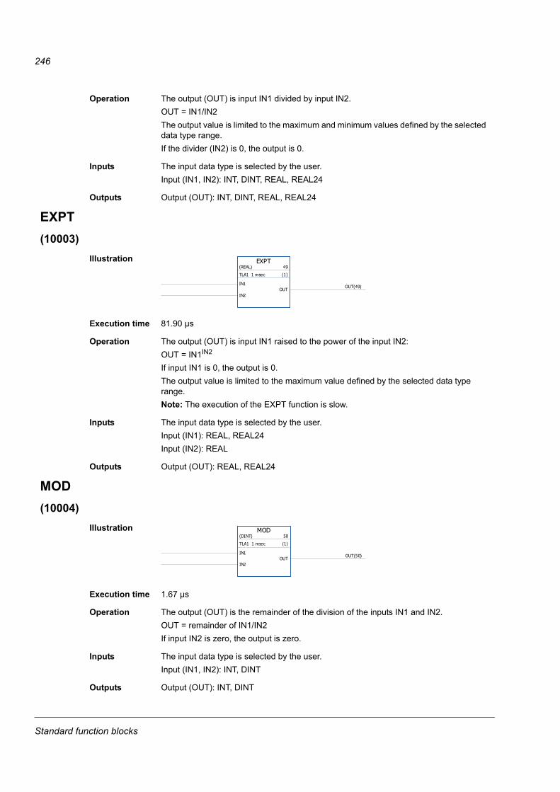
246
Operation The output (OUT) is input IN1 divided by input IN2.OUT = IN1/IN2The output value is limited to the maximum and minimum values defined by the selected data type range.If the divider (IN2) is 0, the output is 0.
Inputs The input data type is selected by the user.Input (IN1, IN2): INT, DINT, REAL, REAL24
Outputs Output (OUT): INT, DINT, REAL, REAL24
EXPT(10003)
Illustration
Execution time 81.90 µs
Operation The output (OUT) is input IN1 raised to the power of the input IN2:OUT = IN1IN2
If input IN1 is 0, the output is 0.The output value is limited to the maximum value defined by the selected data type range.Note: The execution of the EXPT function is slow.
Inputs The input data type is selected by the user.Input (IN1): REAL, REAL24Input (IN2): REAL
Outputs Output (OUT): REAL, REAL24
MOD(10004)
Illustration
Execution time 1.67 µs
Operation The output (OUT) is the remainder of the division of the inputs IN1 and IN2.OUT = remainder of IN1/IN2If input IN2 is zero, the output is zero.
Inputs The input data type is selected by the user.Input (IN1, IN2): INT, DINT
Outputs Output (OUT): INT, DINT
EXPT(REAL) 49
TLA1 1 msec (1)
IN1
IN2OUT
OUT(49)
MOD(DINT) 50
TLA1 1 msec (1)
IN1
IN2OUT
OUT(50)
Standard function blocks

247
MOVE(10005)
Illustration
Execution time 2.10 µs (when two inputs are used) + 0.42 µs (for every additional input). When all inputs are used, the execution time is 14.55 µs.
Operation Copies the input values (IN1…32) to the corresponding outputs (OUT1…32).
Inputs The input data type and number of inputs (2…32) are selected by the user.Input (IN1…IN32): INT, DINT, REAL, REAL24, Boolean
Outputs Output (OUT1…OUT32): INT, DINT, REAL, REAL24, Boolean
MUL(10006)
Illustration
Execution time 3.47 µs (when two inputs are used) + 2.28 µs (for every additional input). When all inputs are used, the execution time is 71.73 µs.
Operation The output (OUT) is the product of the inputs (IN).O = IN1 × IN2 × … × IN32The output value is limited to the maximum and minimum values defined by the selected data type range.
Inputs The input data type and the number of inputs (2…32) are selected by the user.Input (IN1…IN32): INT, DINT, REAL, REAL24
Outputs Output (OUT): INT, DINT, REAL, REAL24
MULDIV(10007)
Illustration
Execution time 7.10 µs
MOVE(BOOL) 51
TLA1 1 msec (1)
IN1
IN2OUT1
OUT1(51)
OUT2OUT2(51)
MUL(DINT) 52
TLA1 1 msec (1)
IN1
IN2OUT
OUT(52)
MULDIV53
TLA1 1 msec (1)
I
MUL
DIV
OO(53)
REMREM(53)
Standard function blocks
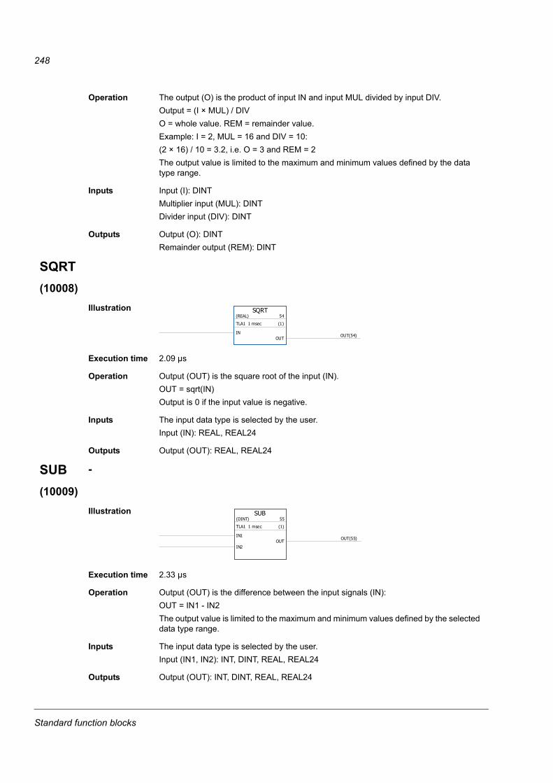
248
Operation The output (O) is the product of input IN and input MUL divided by input DIV.Output = (I × MUL) / DIVO = whole value. REM = remainder value.Example: I = 2, MUL = 16 and DIV = 10:(2 × 16) / 10 = 3.2, i.e. O = 3 and REM = 2The output value is limited to the maximum and minimum values defined by the data type range.
Inputs Input (I): DINTMultiplier input (MUL): DINTDivider input (DIV): DINT
Outputs Output (O): DINTRemainder output (REM): DINT
SQRT(10008)
Illustration
Execution time 2.09 µs
Operation Output (OUT) is the square root of the input (IN).OUT = sqrt(IN)Output is 0 if the input value is negative.
Inputs The input data type is selected by the user.Input (IN): REAL, REAL24
Outputs Output (OUT): REAL, REAL24
SUB -
(10009)Illustration
Execution time 2.33 µs
Operation Output (OUT) is the difference between the input signals (IN):OUT = IN1 - IN2The output value is limited to the maximum and minimum values defined by the selected data type range.
Inputs The input data type is selected by the user.Input (IN1, IN2): INT, DINT, REAL, REAL24
Outputs Output (OUT): INT, DINT, REAL, REAL24
SQRT(REAL) 54
TLA1 1 msec (1)
INOUT
OUT(54)
SUB(DINT) 55
TLA1 1 msec (1)
IN1
IN2OUT
OUT(55)
Standard function blocks
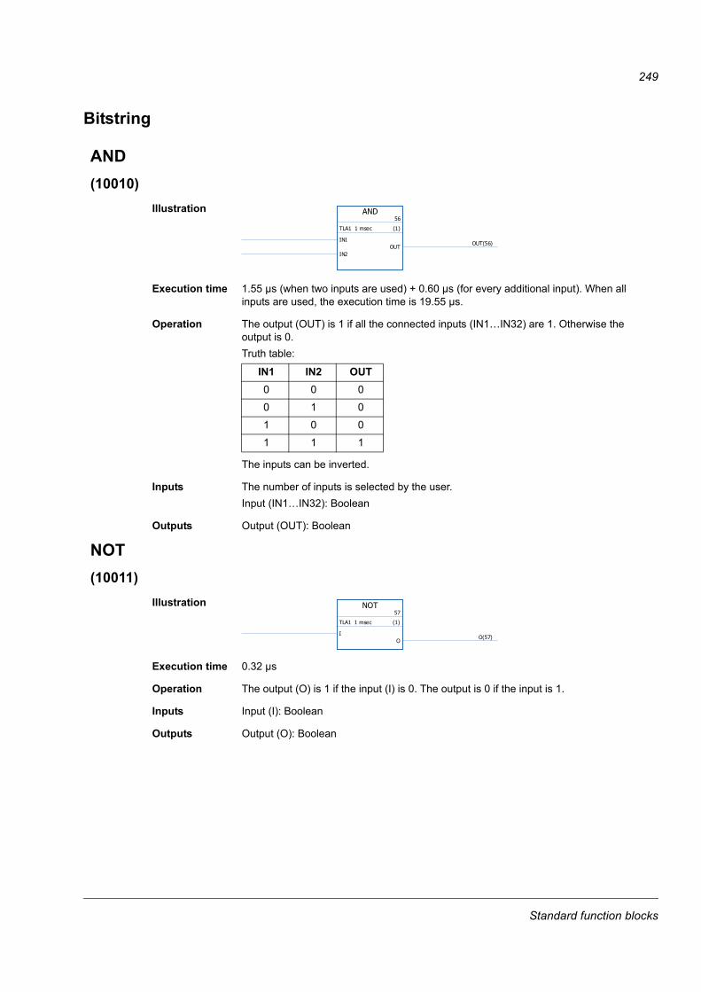
249
Bitstring
AND(10010)
Illustration
Execution time 1.55 µs (when two inputs are used) + 0.60 µs (for every additional input). When all inputs are used, the execution time is 19.55 µs.
Operation The output (OUT) is 1 if all the connected inputs (IN1…IN32) are 1. Otherwise the output is 0.Truth table:
The inputs can be inverted.
Inputs The number of inputs is selected by the user.Input (IN1…IN32): Boolean
Outputs Output (OUT): Boolean
NOT(10011)
Illustration
Execution time 0.32 µs
Operation The output (O) is 1 if the input (I) is 0. The output is 0 if the input is 1.
Inputs Input (I): Boolean
Outputs Output (O): Boolean
AND56
TLA1 1 msec (1)
IN1
IN2OUT
OUT(56)
IN1 IN2 OUT0 0 0
0 1 0
1 0 0
1 1 1
NOT57
TLA1 1 msec (1)
IO
O(57)
Standard function blocks

250
OR(10012)
Illustration
Execution time 1.55 µs (when two inputs are used) + 0.60 µs (for every additional input). When all inputs are used, the execution time is 19.55 µs.
Operation The output (OUT) is 0, if all connected inputs (IN) are 0. Otherwise the output is 1.Truth table:
The inputs can be inverted.
Inputs The number of inputs (2…32) is selected by the user.Input (IN1…IN32): Boolean
Outputs Output (OUT): Boolean
ROL(10013)
Illustration
Execution time 1.28 µs
Operation Input bits (I) are rotated to the left by the number (N) of bits defined by BITCNT. The N most significant bits (MSB) of the input are stored as the N least significant bits (LSB) of the output.Example: If BITCNT = 3
Inputs The input data type is selected by the user.Number of bits input (BITCNT): INT, DINTInput (I): INT, DINT
OR58
TLA1 1 msec (1)
IN1
IN2OUT
OUT(58)
IN1 IN2 OUT0 0 0
0 1 1
1 0 1
1 1 1
ROL(DINT) 59
TLA1 1 msec (1)
BITCNT
IO
O(59)
I 1 1 1 0 0 0 0 0 1 1 1 0 0 1 0 1 1 1 0 1 0 0 1 1 0 0 1 1 0 1 0 1
O 0 0 0 0 0 1 1 1 0 0 1 0 1 1 1 0 1 0 0 1 1 0 0 1 1 0 1 0 1 1 1 1
3 MSB
3 LSB
Standard function blocks

251
Outputs Output (O): INT, DINT
ROR(10014)
Illustration
Execution time 1.28 µs
Operation Input bits (I) are rotated to the right by the number (N) of bits defined by BITCNT. The N least significant bits (LSB) of the input are stored as the N most significant bits (MSB) of the output.Example: If BITCNT = 3
Inputs The input data type is selected by the user.Number of bits input (BITCNT): INT, DINTInput (I): INT, DINT
Outputs Output (O): INT, DINT
SHL(10015)
Illustration
Execution time 0.80 µs
Operation Input bits (I) are rotated to the left by the number (N) of bits defined by BITCNT. The N most significant bits (MSB) of the input are lost and the N least significant bits (LSB) of the output are set to 0.Example: If BITCNT = 3
ROR(DINT) 60
TLA1 1 msec (1)
BITCNT
IO
O(60)
I 1 1 1 0 0 0 0 0 1 1 1 0 0 1 0 1 1 1 0 1 0 0 1 1 0 0 1 1 0 1 0 1
O 1 0 1 1 1 1 0 0 0 0 0 1 1 1 0 0 1 0 1 1 1 0 1 0 0 1 1 0 0 1 1 0
3 MSB
3 LSB
SHL(DINT) 61
TLA1 1 msec (1)
BITCNT
IO
O(61)
I 1 1 1 0 0 0 0 0 1 1 1 0 0 1 0 1 1 1 0 1 0 0 1 1 0 0 1 1 0 1 0 1
O 0 0 0 0 0 1 1 1 0 0 1 0 1 1 1 0 1 0 0 1 1 0 0 1 1 0 1 0 1 0 0 0
3 MSB
3 LSB
Standard function blocks
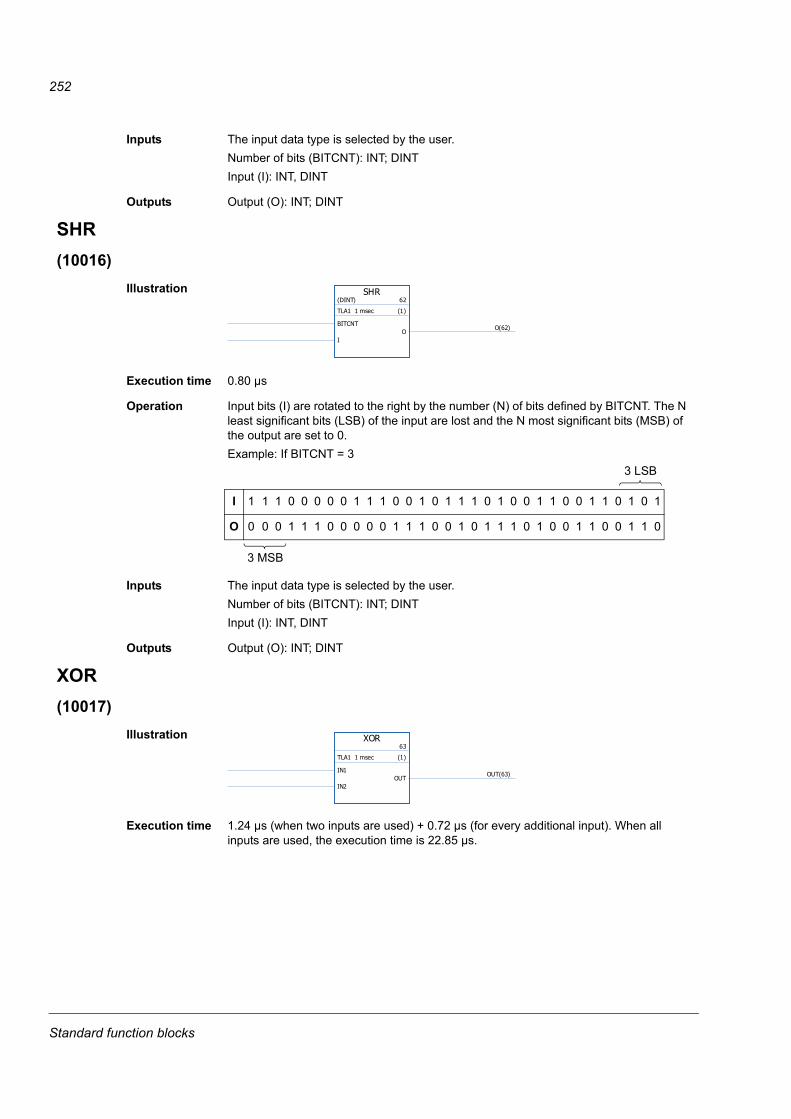
252
Inputs The input data type is selected by the user.Number of bits (BITCNT): INT; DINTInput (I): INT, DINT
Outputs Output (O): INT; DINT
SHR(10016)
Illustration
Execution time 0.80 µs
Operation Input bits (I) are rotated to the right by the number (N) of bits defined by BITCNT. The N least significant bits (LSB) of the input are lost and the N most significant bits (MSB) of the output are set to 0.Example: If BITCNT = 3
Inputs The input data type is selected by the user.Number of bits (BITCNT): INT; DINTInput (I): INT, DINT
Outputs Output (O): INT; DINT
XOR(10017)
Illustration
Execution time 1.24 µs (when two inputs are used) + 0.72 µs (for every additional input). When all inputs are used, the execution time is 22.85 µs.
SHR(DINT) 62
TLA1 1 msec (1)
BITCNT
IO
O(62)
I 1 1 1 0 0 0 0 0 1 1 1 0 0 1 0 1 1 1 0 1 0 0 1 1 0 0 1 1 0 1 0 1
O 0 0 0 1 1 1 0 0 0 0 0 1 1 1 0 0 1 0 1 1 1 0 1 0 0 1 1 0 0 1 1 0
3 MSB
3 LSB
XOR63
TLA1 1 msec (1)
IN1
IN2OUT
OUT(63)
Standard function blocks

253
Operation The output (OUT) is 1 if one of the connected inputs (IN1…IN32) is 1. Output is zero if all the inputs have the same value.Example:
The inputs can be inverted.
Inputs The number of inputs (2…32) is selected by the user.Input (IN1…IN32): Boolean
Outputs Output (OUT): Boolean
IN1 IN2 OUT0 0 0
0 1 1
1 0 1
1 1 0
Standard function blocks
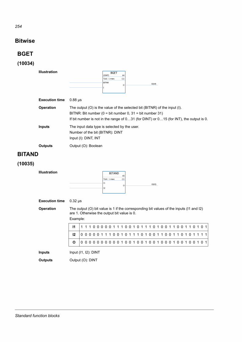
254
Bitwise
BGET (10034)
Illustration
Execution time 0.88 µs
Operation The output (O) is the value of the selected bit (BITNR) of the input (I).BITNR: Bit number (0 = bit number 0, 31 = bit number 31)If bit number is not in the range of 0…31 (for DINT) or 0…15 (for INT), the output is 0.
Inputs The input data type is selected by the user.Number of the bit (BITNR): DINT Input (I): DINT, INT
Outputs Output (O): Boolean
BITAND(10035)
Illustration
Execution time 0.32 µs
Operation The output (O) bit value is 1 if the corresponding bit values of the inputs (I1 and I2) are 1. Otherwise the output bit value is 0.Example:
Inputs Input (I1, I2): DINT
Outputs Output (O): DINT
BGET(DINT) 64
TLA1 1 msec (1)
BITNR
IO
O(64)
BITAND65
TLA1 1 msec (1)
I1
I2O
O(65)
I1 1 1 1 0 0 0 0 0 1 1 1 0 0 1 0 1 1 1 0 1 0 0 1 1 0 0 1 1 0 1 0 1
I2 0 0 0 0 0 1 1 1 0 0 1 0 1 1 1 0 1 0 0 1 1 0 0 1 1 0 1 0 1 1 1 1
O 0 0 0 0 0 0 0 0 0 0 1 0 0 1 0 0 1 0 0 1 0 0 0 1 0 0 1 0 0 1 0 1
Standard function blocks
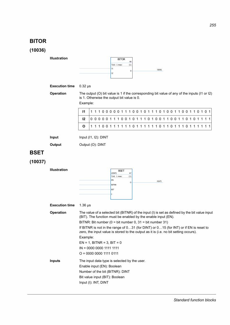
255
BITOR(10036)
Illustration
Execution time 0.32 µs
Operation The output (O) bit value is 1 if the corresponding bit value of any of the inputs (I1 or I2) is 1. Otherwise the output bit value is 0.Example:
Input Input (I1, I2): DINT
Output Output (O): DINT
BSET(10037)
Illustration
Execution time 1.36 µs
Operation The value of a selected bit (BITNR) of the input (I) is set as defined by the bit value input (BIT). The function must be enabled by the enable input (EN).BITNR: Bit number (0 = bit number 0, 31 = bit number 31)If BITNR is not in the range of 0…31 (for DINT) or 0…15 (for INT) or if EN is reset to zero, the input value is stored to the output as it is (i.e. no bit setting occurs).Example:EN = 1, BITNR = 3, BIT = 0IN = 0000 0000 1111 1111O = 0000 0000 1111 0111
Inputs The input data type is selected by the user.Enable input (EN): BooleanNumber of the bit (BITNR): DINTBit value input (BIT): BooleanInput (I): INT, DINT
BITOR66
TLA1 1 msec (1)
I1
I2O
O(66)
I1 1 1 1 0 0 0 0 0 1 1 1 0 0 1 0 1 1 1 0 1 0 0 1 1 0 0 1 1 0 1 0 1
I2 0 0 0 0 0 1 1 1 0 0 1 0 1 1 1 0 1 0 0 1 1 0 0 1 1 0 1 0 1 1 1 1
O 1 1 1 0 0 1 1 1 1 1 1 0 1 1 1 1 1 1 0 1 1 0 1 1 1 0 1 1 1 1 1 1
BSET(DINT) 67
TLA1 1 msec (1)
EN
BITNR
BIT
I
OO(67)
Standard function blocks

256
Outputs Output (O): INT, DINT
REG(10038)
Illustration
Execution time 2.27 µs (when two inputs are used) + 1.02 µs (for every additional input). When all inputs are used, the execution time is 32.87 µs.
Operation The input (I1…I32) value is stored to the corresponding output (O1…O32) if the load input (L) is set to 1 or the set input (S) is 1. When the load input is set to 1, the input value is stored to the output only once. When the set input is 1, the input value is stored to the output every time the block is executed. The set input overrides the load input.If the reset input (R) is 1, all connected outputs are 0.Example:
Inputs The input data type and number of inputs (1…32) are selected by the user.Set input (S): BooleanLoad input (L): BooleanReset input (R): Boolean Input (I1…I32): Boolean, INT, DINT, REAL, REAL24
Outputs Output (O1…O32): Boolean, INT, DINT, REAL, REAL24
REG(BOOL) 68
TLA1 1 msec (1)
S
>L
R
I1
I2
O1O1(68)
O2O2(68)
S R L I O1previous O10 0 0 10 15 15
0 0 0->1 20 15 20
0 1 0 30 20 0
0 1 0->1 40 0 0
1 0 0 50 0 50
1 0 0->1 60 50 60
1 1 0 70 60 0
1 1 0->1 80 0 0
O1previous is the previous cycle output value.
Standard function blocks

257
SR-D(10039)
Illustration
Execution time 1.04 µs
Operation When clock input (C) is set to 1, the data input (D) value is stored to the output (O). When reset input (R) is set to 1, the output is set to 0.If only set (S) and reset (R) inputs are used, SR-D block acts as an SR block:The output is 1 if the set input (S) is 1. The output will retain the previous output state if the set input (S) and reset input (R) are 0. The output is 0 if the set input is 0 and the reset input is 1.Truth table:
Inputs Set input (S): BooleanData input (D): BooleanClock input (C): BooleanReset input (R): Boolean
Outputs Output (O): Boolean
SR-D69
TLA1 1 msec (1)
S
D
>C
R
OO(69)
S R D C Oprevious O0 0 0 0 0 0 (= Previous output value)
0 0 0 0 -> 1 0 0 (= Data input value)
0 0 1 0 0 0 (= Previous output value)
0 0 1 0 -> 1 0 1 (= Data input value)
0 1 0 0 1 0 (Reset)
0 1 0 0 -> 1 0 0 (Reset)
0 1 1 0 0 0 (Reset)
0 1 1 0 -> 1 0 0 (Reset)
1 0 0 0 0 1 (= Set value)
1 0 0 0 -> 1 1 0 (= Data input value) for one execution cycle, then changes to 1 according to the set input (S = 1).
1 0 1 0 1 1 (= Set value)
1 0 1 0 -> 1 1 1 (= Data input value)
1 1 0 0 1 0 (Reset)
1 1 0 0 -> 1 0 0 (Reset)
1 1 1 0 0 0 (Reset)
1 1 1 0 -> 1 0 0 (Reset)
Oprevious is the previous cycle output value.
Standard function blocks
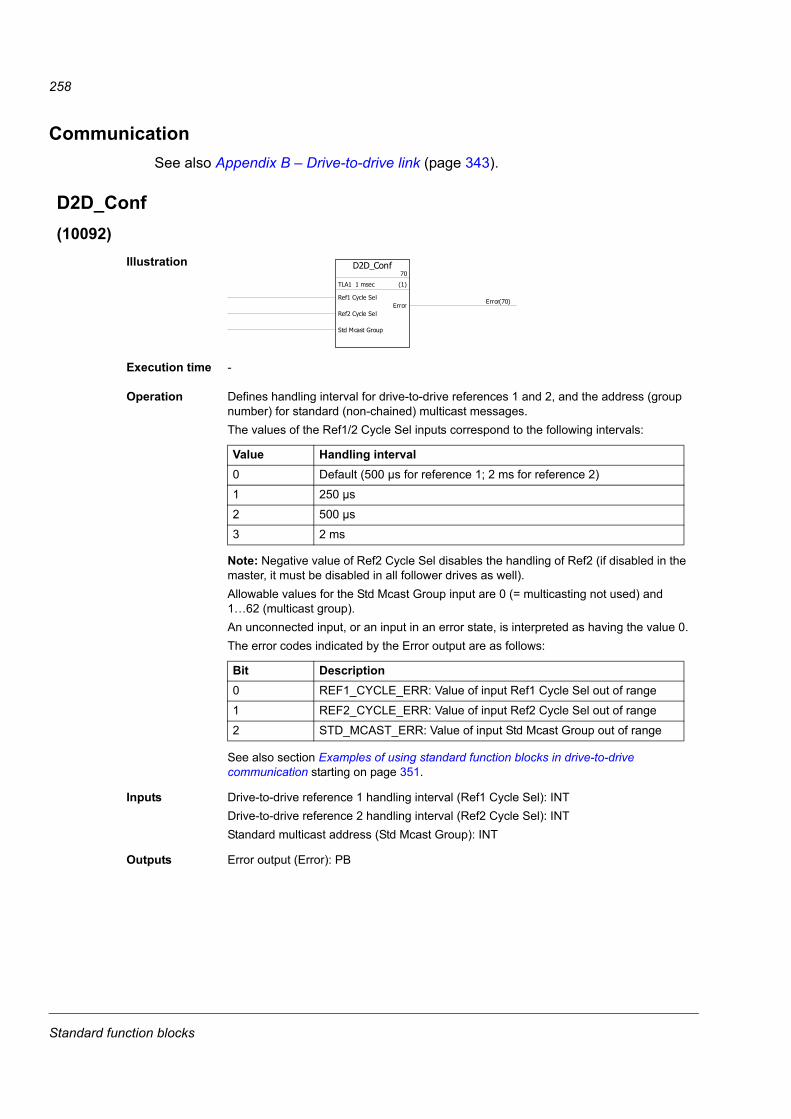
258
CommunicationSee also Appendix B – Drive-to-drive link (page 343).
D2D_Conf(10092)
Illustration
Execution time -
Operation Defines handling interval for drive-to-drive references 1 and 2, and the address (group number) for standard (non-chained) multicast messages.The values of the Ref1/2 Cycle Sel inputs correspond to the following intervals:
Note: Negative value of Ref2 Cycle Sel disables the handling of Ref2 (if disabled in the master, it must be disabled in all follower drives as well).Allowable values for the Std Mcast Group input are 0 (= multicasting not used) and 1…62 (multicast group).An unconnected input, or an input in an error state, is interpreted as having the value 0.The error codes indicated by the Error output are as follows:
See also section Examples of using standard function blocks in drive-to-drive communication starting on page 351.
Inputs Drive-to-drive reference 1 handling interval (Ref1 Cycle Sel): INTDrive-to-drive reference 2 handling interval (Ref2 Cycle Sel): INTStandard multicast address (Std Mcast Group): INT
Outputs Error output (Error): PB
D2D_Conf70
TLA1 1 msec (1)
Ref1 Cycle Sel
Ref2 Cycle Sel
Std Mcast Group
ErrorError(70)
Value Handling interval0 Default (500 µs for reference 1; 2 ms for reference 2)
1 250 µs
2 500 µs
3 2 ms
Bit Description0 REF1_CYCLE_ERR: Value of input Ref1 Cycle Sel out of range
1 REF2_CYCLE_ERR: Value of input Ref2 Cycle Sel out of range
2 STD_MCAST_ERR: Value of input Std Mcast Group out of range
Standard function blocks
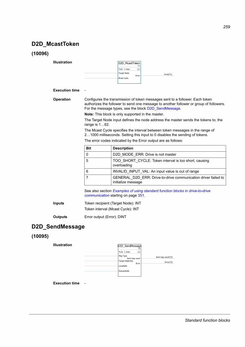
259
D2D_McastToken(10096)
Illustration
Execution time -
Operation Configures the transmission of token messages sent to a follower. Each token authorizes the follower to send one message to another follower or group of followers. For the message types, see the block D2D_SendMessage.Note: This block is only supported in the master.The Target Node input defines the node address the master sends the tokens to; the range is 1…62.The Mcast Cycle specifies the interval between token messages in the range of 2…1000 milliseconds. Setting this input to 0 disables the sending of tokens.The error codes indicated by the Error output are as follows:
See also section Examples of using standard function blocks in drive-to-drive communication starting on page 351.
Inputs Token recipient (Target Node): INTToken interval (Mcast Cycle): INT
Outputs Error output (Error): DINT
D2D_SendMessage(10095)
Illustration
Execution time -
D2D_McastToken71
TLA1 1 msec (1)
Target Node
Mcast CycleError
Error(71)
Bit Description0 D2D_MODE_ERR: Drive is not master
5 TOO_SHORT_CYCLE: Token interval is too short, causing overloading
6 INVALID_INPUT_VAL: An input value is out of range
7 GENERAL_D2D_ERR: Drive-to-drive communication driver failed to initialize message
D2D_SendMessage72
TLA1 1 msec (1)
Msg Type
Target Node/Grp
LocalDsNr
RemoteDsNr
Sent msg countSent msg count(72)
ErrorError(72)
Standard function blocks
260
Operation Configures the transmission between the dataset tables of drives.The Msg Type input defines the message type as follows:
See also section Examples of using standard function blocks in drive-to-drive communication starting on page 351.
Value Message type0 Disabled
1 Master P2P:The master sends the contents of a local dataset (specified by LocalDsNr input) to the dataset table (dataset number specified by RemoteDsNr input) of a follower (specified by Target Node/Grp input).The follower replies by sending the next dataset (RemoteDsNr + 1) to the master (LocalDsNr + 1).The node number of a drive is defined by parameter 57.03.Note: Only supported in the master drive.
2 Read Remote:The master reads a dataset (specified by RemoteDsNr input) from a follower (specified by Target Node/Grp input) and stores it into local dataset table (dataset number specified by LocalDsNr input).The node number of a drive is defined by parameter 57.03.Note: Only supported in the master drive.
3 Follower P2P:The follower sends the contents of a local dataset (specified by LocalDsNr input) to the dataset table (dataset number specified by RemoteDsNr input) of another follower (specified by Target Node/Grp input).The node number of a drive is defined by parameter 57.03.Note: Only supported in a follower drive. A token from the master drive is required for the follower to be able to send the message. See the block D2D_McastToken.
4 Standard Multicast:The drive sends the contents of a local dataset (specified by LocalDsNr input) to the dataset table (dataset number specified by RemoteDsNr input) of a group of followers (specified by Target Node/Grp input).Which multicast group a drive belongs to is defined by the Std Mcast Group input of the D2D_Conf block.A token from the master drive is required for a follower to be able to send the message. See the block D2D_McastToken.
5 Broadcast:The drive sends the contents of a local dataset (specified by LocalDsNr input) to the dataset table (dataset number specified by RemoteDsNr input) of all followers.A token from the master drive is required for a follower to be able to send the message. See the block D2D_McastToken.Note: With this message type, the Target Node/Grp input must be connected in DriveSPC even if not used.
Standard function blocks
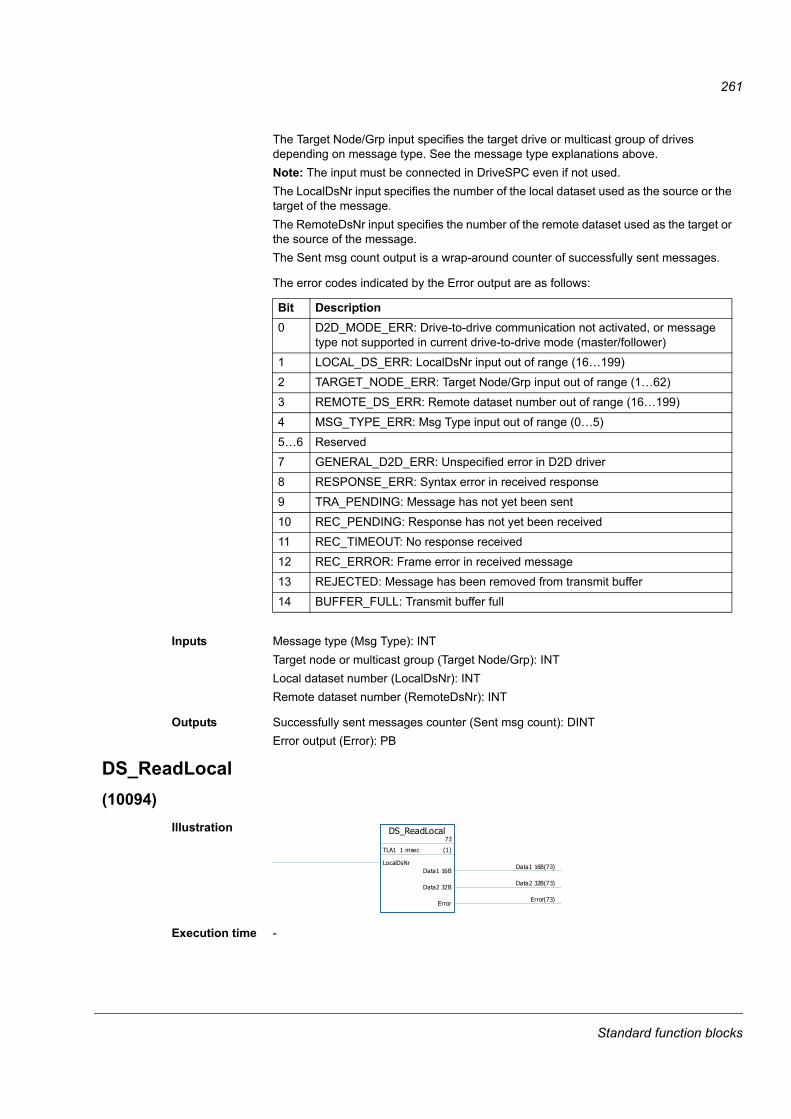
261
The Target Node/Grp input specifies the target drive or multicast group of drives depending on message type. See the message type explanations above.Note: The input must be connected in DriveSPC even if not used.The LocalDsNr input specifies the number of the local dataset used as the source or the target of the message.The RemoteDsNr input specifies the number of the remote dataset used as the target or the source of the message.The Sent msg count output is a wrap-around counter of successfully sent messages.
The error codes indicated by the Error output are as follows:
Inputs Message type (Msg Type): INTTarget node or multicast group (Target Node/Grp): INTLocal dataset number (LocalDsNr): INTRemote dataset number (RemoteDsNr): INT
Outputs Successfully sent messages counter (Sent msg count): DINTError output (Error): PB
DS_ReadLocal(10094)
Illustration
Execution time -
Bit Description0 D2D_MODE_ERR: Drive-to-drive communication not activated, or message
type not supported in current drive-to-drive mode (master/follower)
1 LOCAL_DS_ERR: LocalDsNr input out of range (16…199)
2 TARGET_NODE_ERR: Target Node/Grp input out of range (1…62)
3 REMOTE_DS_ERR: Remote dataset number out of range (16…199)
4 MSG_TYPE_ERR: Msg Type input out of range (0…5)
5…6 Reserved
7 GENERAL_D2D_ERR: Unspecified error in D2D driver
8 RESPONSE_ERR: Syntax error in received response
9 TRA_PENDING: Message has not yet been sent
10 REC_PENDING: Response has not yet been received
11 REC_TIMEOUT: No response received
12 REC_ERROR: Frame error in received message
13 REJECTED: Message has been removed from transmit buffer
14 BUFFER_FULL: Transmit buffer full
DS_ReadLocal73
TLA1 1 msec (1)
LocalDsNrData1 16B
Data1 16B(73)
Data2 32BData2 32B(73)
ErrorError(73)
Standard function blocks
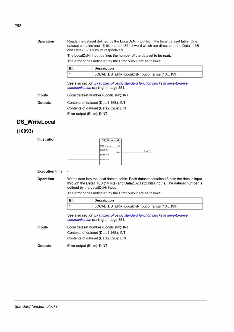
262
Operation Reads the dataset defined by the LocalDsNr input from the local dataset table. One dataset contains one 16-bit and one 32-bit word which are directed to the Data1 16B and Data2 32B outputs respectively.The LocalDsNr input defines the number of the dataset to be read.The error codes indicated by the Error output are as follows:
See also section Examples of using standard function blocks in drive-to-drive communication starting on page 351.
Inputs Local dataset number (LocalDsNr): INT
Outputs Contents of dataset (Data1 16B): INTContents of dataset (Data2 32B): DINTError output (Error): DINT
DS_WriteLocal(10093)
Illustration
Execution time -
Operation Writes data into the local dataset table. Each dataset contains 48 bits; the data is input through the Data1 16B (16 bits) and Data2 32B (32 bits) inputs. The dataset number is defined by the LocalDsNr input.The error codes indicated by the Error output are as follows:
See also section Examples of using standard function blocks in drive-to-drive communication starting on page 351.
Inputs Local dataset number (LocalDsNr): INTContents of dataset (Data1 16B): INTContents of dataset (Data2 32B): DINT
Outputs Error output (Error): DINT
Bit Description1 LOCAL_DS_ERR: LocalDsNr out of range (16…199)
DS_WriteLocal74
TLA1 1 msec (1)
LocalDsNr
Data1 16B
Data2 32B
ErrorError(74)
Bit Description1 LOCAL_DS_ERR: LocalDsNr out of range (16…199)
Standard function blocks
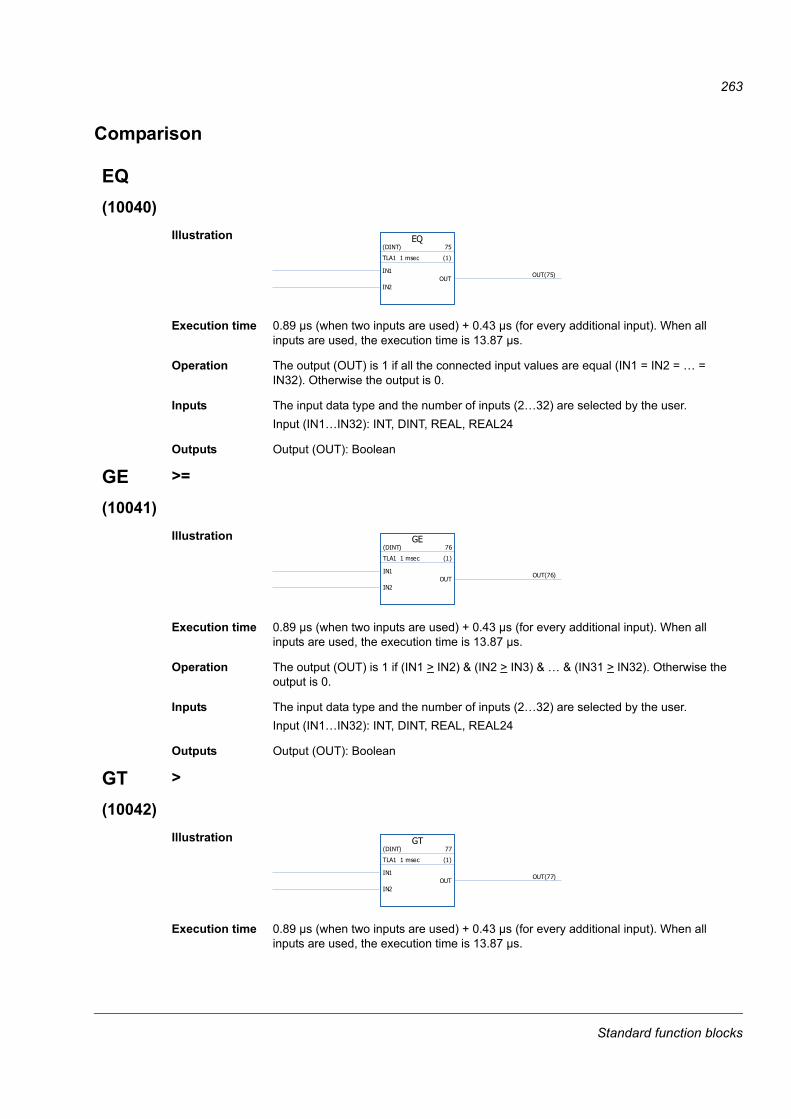
263
Comparison
EQ(10040)
Illustration
Execution time 0.89 µs (when two inputs are used) + 0.43 µs (for every additional input). When all inputs are used, the execution time is 13.87 µs.
Operation The output (OUT) is 1 if all the connected input values are equal (IN1 = IN2 = … = IN32). Otherwise the output is 0.
Inputs The input data type and the number of inputs (2…32) are selected by the user.Input (IN1…IN32): INT, DINT, REAL, REAL24
Outputs Output (OUT): Boolean
GE >=
(10041)Illustration
Execution time 0.89 µs (when two inputs are used) + 0.43 µs (for every additional input). When all inputs are used, the execution time is 13.87 µs.
Operation The output (OUT) is 1 if (IN1 > IN2) & (IN2 > IN3) & … & (IN31 > IN32). Otherwise the output is 0.
Inputs The input data type and the number of inputs (2…32) are selected by the user.Input (IN1…IN32): INT, DINT, REAL, REAL24
Outputs Output (OUT): Boolean
GT >
(10042)Illustration
Execution time 0.89 µs (when two inputs are used) + 0.43 µs (for every additional input). When all inputs are used, the execution time is 13.87 µs.
EQ(DINT) 75
TLA1 1 msec (1)
IN1
IN2OUT
OUT(75)
GE(DINT) 76
TLA1 1 msec (1)
IN1
IN2OUT
OUT(76)
GT(DINT) 77
TLA1 1 msec (1)
IN1
IN2OUT
OUT(77)
Standard function blocks
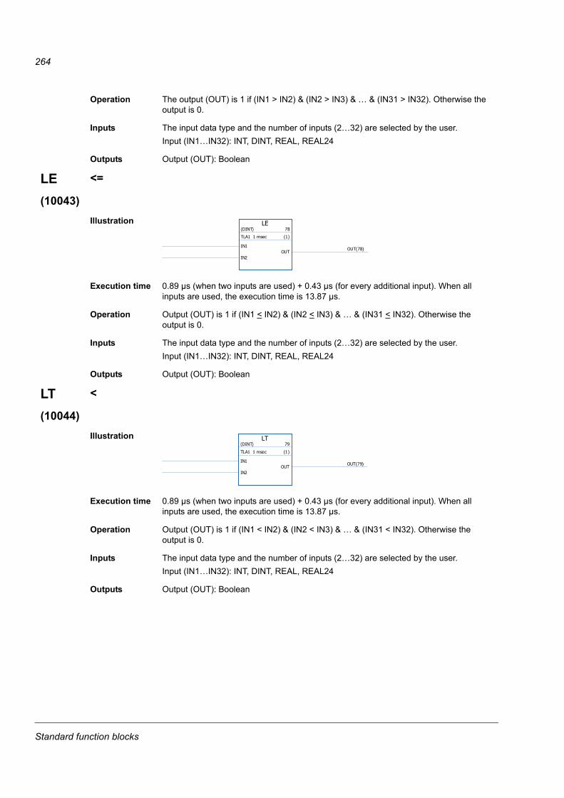
264
Operation The output (OUT) is 1 if (IN1 > IN2) & (IN2 > IN3) & … & (IN31 > IN32). Otherwise the output is 0.
Inputs The input data type and the number of inputs (2…32) are selected by the user.Input (IN1…IN32): INT, DINT, REAL, REAL24
Outputs Output (OUT): Boolean
LE <=
(10043)Illustration
Execution time 0.89 µs (when two inputs are used) + 0.43 µs (for every additional input). When all inputs are used, the execution time is 13.87 µs.
Operation Output (OUT) is 1 if (IN1 < IN2) & (IN2 < IN3) & … & (IN31 < IN32). Otherwise the output is 0.
Inputs The input data type and the number of inputs (2…32) are selected by the user.Input (IN1…IN32): INT, DINT, REAL, REAL24
Outputs Output (OUT): Boolean
LT <
(10044)Illustration
Execution time 0.89 µs (when two inputs are used) + 0.43 µs (for every additional input). When all inputs are used, the execution time is 13.87 µs.
Operation Output (OUT) is 1 if (IN1 < IN2) & (IN2 < IN3) & … & (IN31 < IN32). Otherwise the output is 0.
Inputs The input data type and the number of inputs (2…32) are selected by the user.Input (IN1…IN32): INT, DINT, REAL, REAL24
Outputs Output (OUT): Boolean
LE(DINT) 78
TLA1 1 msec (1)
IN1
IN2OUT
OUT(78)
LT(DINT) 79
TLA1 1 msec (1)
IN1
IN2OUT
OUT(79)
Standard function blocks
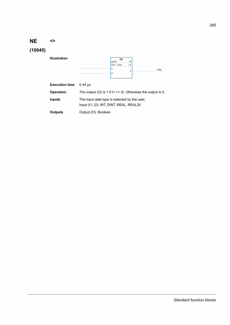
265
NE <>
(10045)Illustration
Execution time 0.44 µs
Operation The output (O) is 1 if I1 <> I2. Otherwise the output is 0.
Inputs The input data type is selected by the user.Input (I1, I2): INT, DINT, REAL, REAL24
Outputs Output (O): Boolean
NE(DINT) 80
TLA1 1 msec (1)
I1
I2O
O(80)
Standard function blocks
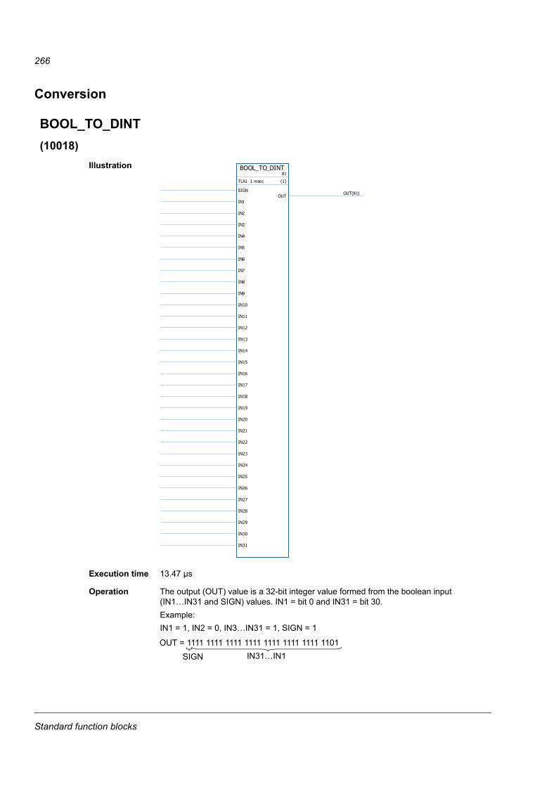
266
Conversion
BOOL_TO_DINT(10018)
Illustration
Execution time 13.47 µs
Operation The output (OUT) value is a 32-bit integer value formed from the boolean input (IN1…IN31 and SIGN) values. IN1 = bit 0 and IN31 = bit 30.Example:IN1 = 1, IN2 = 0, IN3…IN31 = 1, SIGN = 1
BOOL_TO_DINT81
TLA1 1 msec (1)
SIGN
IN1
IN2
IN3
IN4
IN5
IN6
IN7
IN8
IN9
IN10
IN11
IN12
IN13
IN14
IN15
IN16
IN17
IN18
IN19
IN20
IN21
IN22
IN23
IN24
IN25
IN26
IN27
IN28
IN29
IN30
IN31
OUTOUT(81)
OUT = 1111 1111 1111 1111 1111 1111 1111 1101IN31…IN1SIGN
Standard function blocks
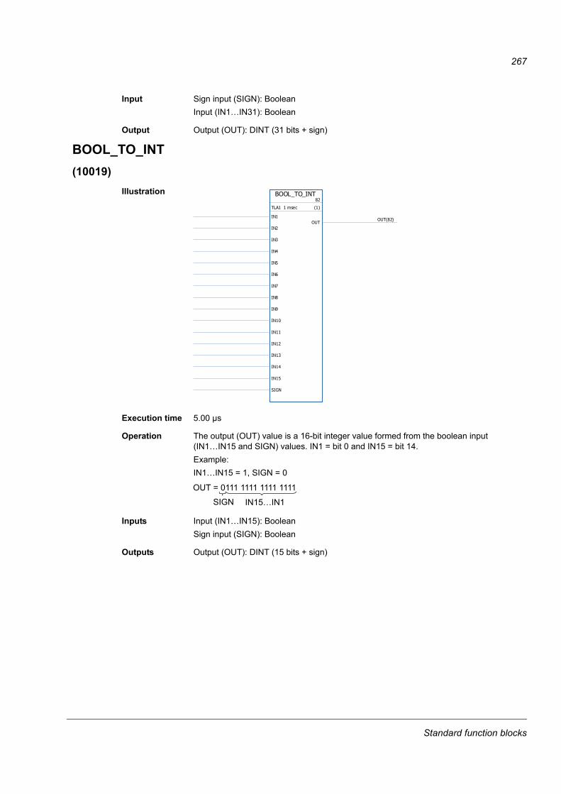
267
Input Sign input (SIGN): BooleanInput (IN1…IN31): Boolean
Output Output (OUT): DINT (31 bits + sign)
BOOL_TO_INT(10019)
Illustration
Execution time 5.00 µs
Operation The output (OUT) value is a 16-bit integer value formed from the boolean input (IN1…IN15 and SIGN) values. IN1 = bit 0 and IN15 = bit 14.Example:IN1…IN15 = 1, SIGN = 0
Inputs Input (IN1…IN15): BooleanSign input (SIGN): Boolean
Outputs Output (OUT): DINT (15 bits + sign)
BOOL_TO_INT82
TLA1 1 msec (1)
IN1
IN2
IN3
IN4
IN5
IN6
IN7
IN8
IN9
IN10
IN11
IN12
IN13
IN14
IN15
SIGN
OUTOUT(82)
OUT = 0111 1111 1111 1111
IN15…IN1SIGN
Standard function blocks

268
DINT_TO_BOOL(10020)
Illustration
Execution time 11.98 µs
Operation The boolean output (OUT1…OUT32) values are formed from the 32-bit integer input (IN) value.Example:
Inputs Input (IN): DINT
Outputs Output (OUT1…OUT32): BooleanSign output (SIGN): Boolean
DINT_TO_BOOL83
TLA1 1 msec (1)
INOUT1
OUT1(83)
OUT2OUT2(83)
OUT3OUT3(83)
OUT4OUT4(83)
OUT5OUT5(83)
OUT6OUT6(83)
OUT7OUT7(83)
OUT8OUT8(83)
OUT9OUT9(83)
OUT10OUT10(83)
OUT11OUT11(83)
OUT12OUT12(83)
OUT13OUT13(83)
OUT14OUT14(83)
OUT15OUT15(83)
OUT16OUT16(83)
OUT17OUT17(83)
OUT18OUT18(83)
OUT19OUT19(83)
OUT20OUT20(83)
OUT21OUT21(83)
OUT22OUT22(83)
OUT23OUT23(83)
OUT24OUT24(83)
OUT25OUT25(83)
OUT26OUT26(83)
OUT27OUT27(83)
OUT28OUT28(83)
OUT29OUT29(83)
OUT30OUT30(83)
OUT31OUT31(83)
OUT32OUT32(83)
SIGNSIGN(83)
IN = 0 111 1111 1111 1111 1111 1111 1111 1100OUT32…OUT1SIGN
Standard function blocks
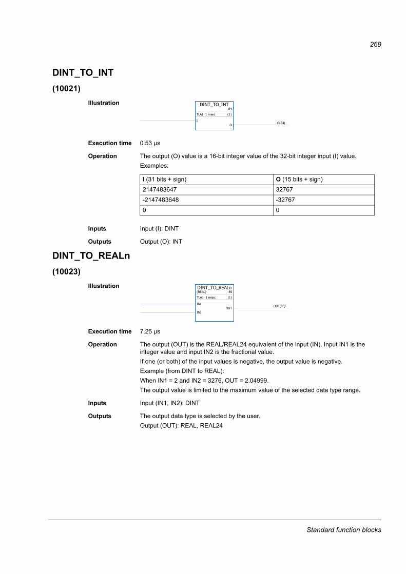
269
DINT_TO_INT(10021)
Illustration
Execution time 0.53 µs
Operation The output (O) value is a 16-bit integer value of the 32-bit integer input (I) value.Examples:
Inputs Input (I): DINT
Outputs Output (O): INT
DINT_TO_REALn(10023)
Illustration
Execution time 7.25 µs
Operation The output (OUT) is the REAL/REAL24 equivalent of the input (IN). Input IN1 is the integer value and input IN2 is the fractional value.If one (or both) of the input values is negative, the output value is negative.Example (from DINT to REAL):When IN1 = 2 and IN2 = 3276, OUT = 2.04999.The output value is limited to the maximum value of the selected data type range.
Inputs Input (IN1, IN2): DINT
Outputs The output data type is selected by the user.Output (OUT): REAL, REAL24
DINT_TO_INT84
TLA1 1 msec (1)
IO
O(84)
I (31 bits + sign) O (15 bits + sign)
2147483647 32767
-2147483648 -32767
0 0
DINT_TO_REALn(REAL) 85
TLA1 1 msec (1)
IN1
IN2OUT
OUT(85)
Standard function blocks
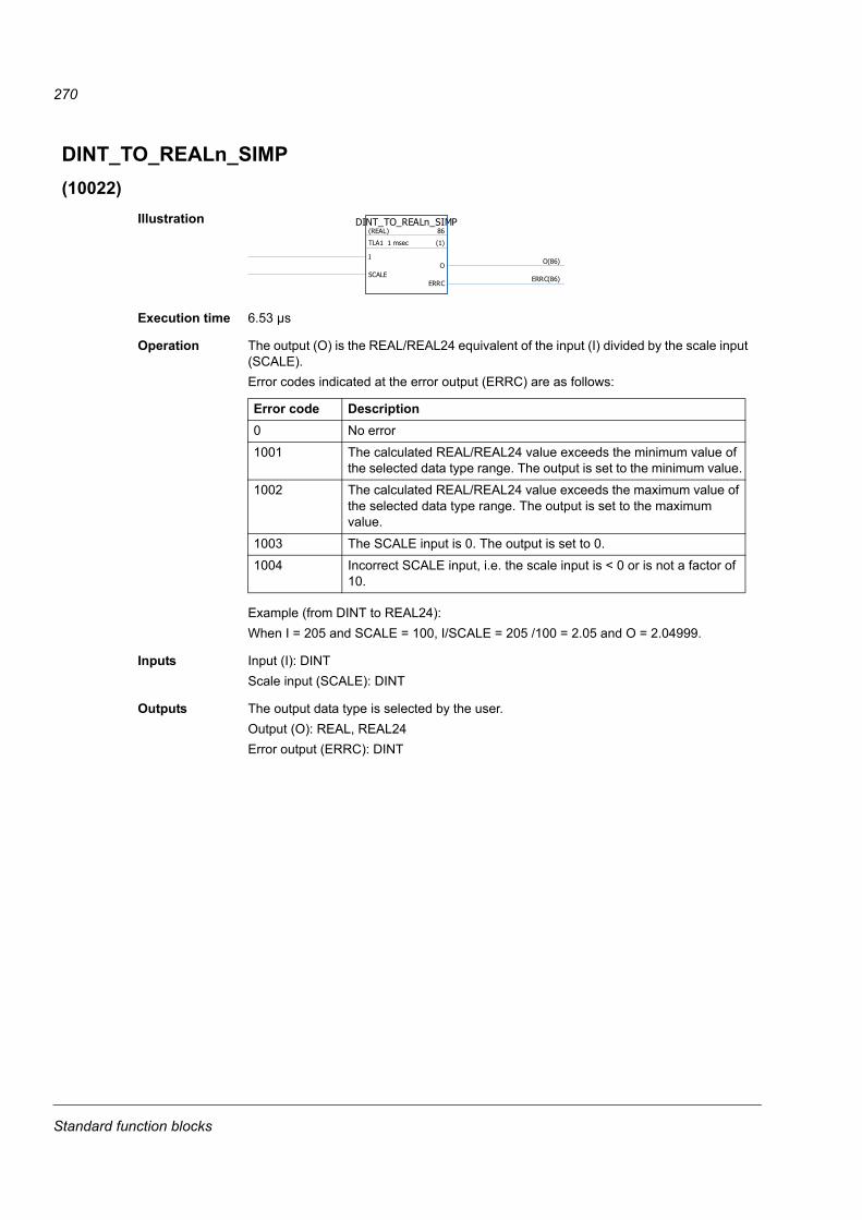
270
DINT_TO_REALn_SIMP(10022)
Illustration
Execution time 6.53 µs
Operation The output (O) is the REAL/REAL24 equivalent of the input (I) divided by the scale input (SCALE). Error codes indicated at the error output (ERRC) are as follows:
Example (from DINT to REAL24):When I = 205 and SCALE = 100, I/SCALE = 205 /100 = 2.05 and O = 2.04999.
Inputs Input (I): DINTScale input (SCALE): DINT
Outputs The output data type is selected by the user.Output (O): REAL, REAL24Error output (ERRC): DINT
DINT_TO_REALn_SIMP(REAL) 86
TLA1 1 msec (1)
I
SCALEO
O(86)
ERRCERRC(86)
Error code Description0 No error
1001 The calculated REAL/REAL24 value exceeds the minimum value of the selected data type range. The output is set to the minimum value.
1002 The calculated REAL/REAL24 value exceeds the maximum value of the selected data type range. The output is set to the maximum value.
1003 The SCALE input is 0. The output is set to 0.
1004 Incorrect SCALE input, i.e. the scale input is < 0 or is not a factor of 10.
Standard function blocks
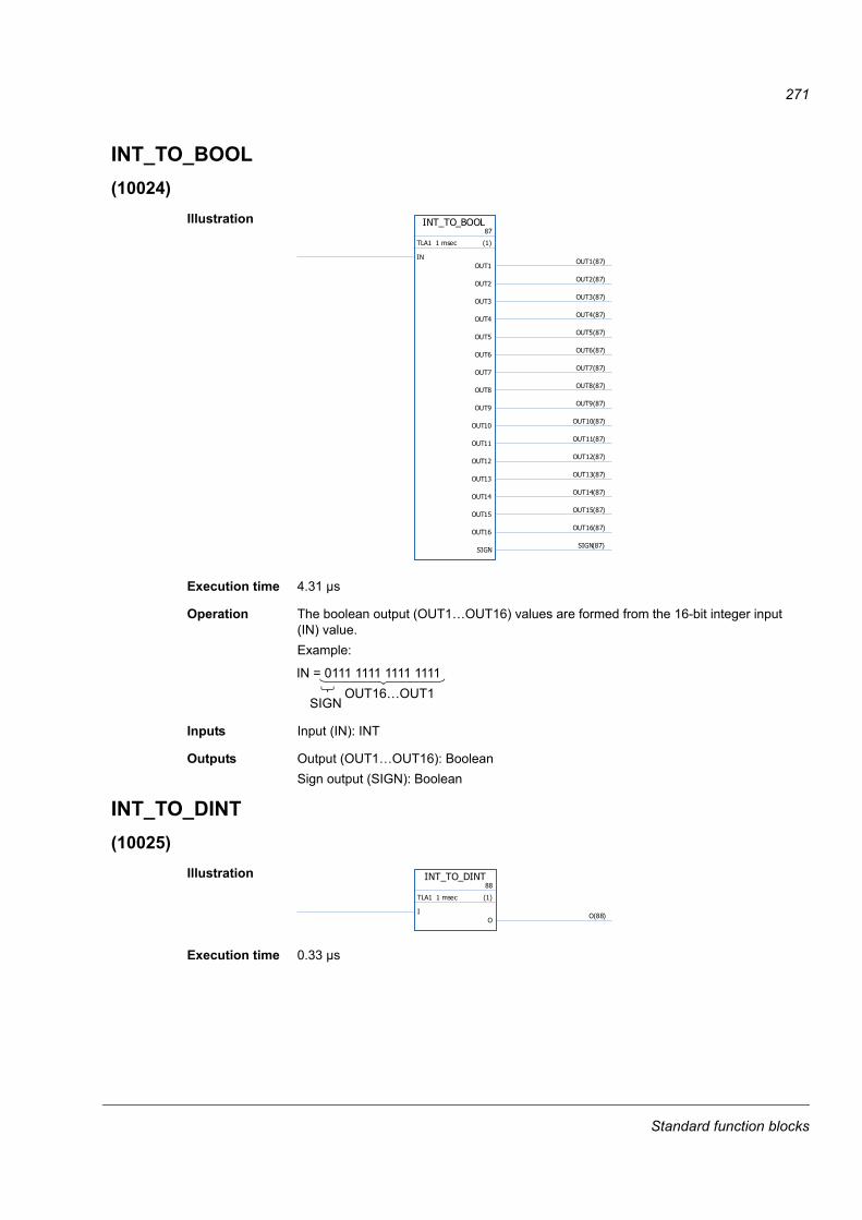
271
INT_TO_BOOL(10024)
Illustration
Execution time 4.31 µs
Operation The boolean output (OUT1…OUT16) values are formed from the 16-bit integer input (IN) value.Example:
Inputs Input (IN): INT
Outputs Output (OUT1…OUT16): BooleanSign output (SIGN): Boolean
INT_TO_DINT(10025)
Illustration
Execution time 0.33 µs
INT_TO_BOOL87
TLA1 1 msec (1)
INOUT1
OUT1(87)
OUT2OUT2(87)
OUT3OUT3(87)
OUT4OUT4(87)
OUT5OUT5(87)
OUT6OUT6(87)
OUT7OUT7(87)
OUT8OUT8(87)
OUT9OUT9(87)
OUT10OUT10(87)
OUT11OUT11(87)
OUT12OUT12(87)
OUT13OUT13(87)
OUT14OUT14(87)
OUT15OUT15(87)
OUT16OUT16(87)
SIGNSIGN(87)
IN = 0111 1111 1111 1111OUT16…OUT1
SIGN
INT_TO_DINT88
TLA1 1 msec (1)
IO
O(88)
Standard function blocks
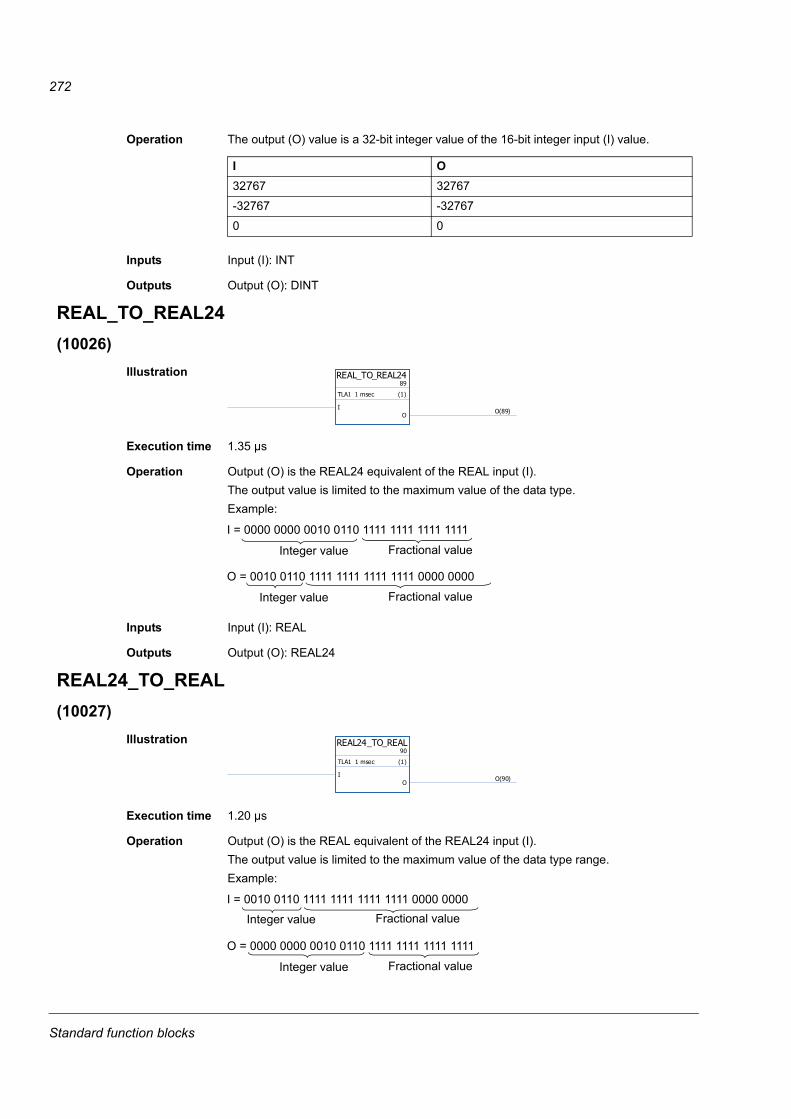
272
Operation The output (O) value is a 32-bit integer value of the 16-bit integer input (I) value.
Inputs Input (I): INT
Outputs Output (O): DINT
REAL_TO_REAL24(10026)
Illustration
Execution time 1.35 µs
Operation Output (O) is the REAL24 equivalent of the REAL input (I). The output value is limited to the maximum value of the data type.Example:
Inputs Input (I): REAL
Outputs Output (O): REAL24
REAL24_TO_REAL(10027)
Illustration
Execution time 1.20 µs
Operation Output (O) is the REAL equivalent of the REAL24 input (I). The output value is limited to the maximum value of the data type range.Example:
I O32767 32767
-32767 -32767
0 0
REAL_TO_REAL2489
TLA1 1 msec (1)
IO
O(89)
I = 0000 0000 0010 0110 1111 1111 1111 1111
Integer value Fractional value
O = 0010 0110 1111 1111 1111 1111 0000 0000
Integer value Fractional value
REAL24_TO_REAL90
TLA1 1 msec (1)
IO
O(90)
I = 0010 0110 1111 1111 1111 1111 0000 0000
Integer value Fractional value
O = 0000 0000 0010 0110 1111 1111 1111 1111
Integer value Fractional value
Standard function blocks
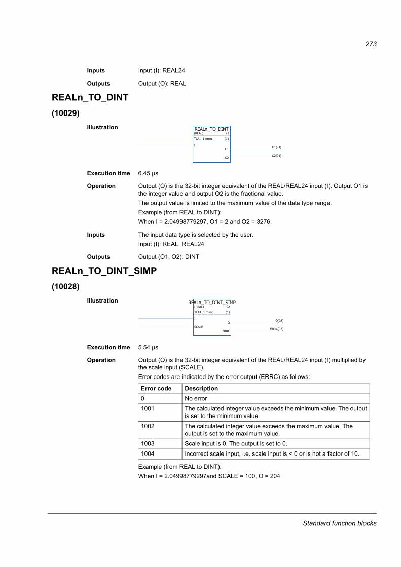
273
Inputs Input (I): REAL24
Outputs Output (O): REAL
REALn_TO_DINT(10029)
Illustration
Execution time 6.45 µs
Operation Output (O) is the 32-bit integer equivalent of the REAL/REAL24 input (I). Output O1 is the integer value and output O2 is the fractional value.The output value is limited to the maximum value of the data type range.Example (from REAL to DINT):When I = 2.04998779297, O1 = 2 and O2 = 3276.
Inputs The input data type is selected by the user.Input (I): REAL, REAL24
Outputs Output (O1, O2): DINT
REALn_TO_DINT_SIMP(10028)
Illustration
Execution time 5.54 µs
Operation Output (O) is the 32-bit integer equivalent of the REAL/REAL24 input (I) multiplied by the scale input (SCALE).Error codes are indicated by the error output (ERRC) as follows:
Example (from REAL to DINT):When I = 2.04998779297and SCALE = 100, O = 204.
REALn_TO_DINT(REAL) 91
TLA1 1 msec (1)
IO1
O1(91)
O2O2(91)
REALn_TO_DINT_SIMP(REAL) 92
TLA1 1 msec (1)
I
SCALEO
O(92)
ERRCERRC(92)
Error code Description0 No error
1001 The calculated integer value exceeds the minimum value. The output is set to the minimum value.
1002 The calculated integer value exceeds the maximum value. The output is set to the maximum value.
1003 Scale input is 0. The output is set to 0.
1004 Incorrect scale input, i.e. scale input is < 0 or is not a factor of 10.
Standard function blocks
274
Inputs The input data type is selected by the user.Input (I): REAL, REAL24Scale input (SCALE): DINT
Outputs Output (O): DINTError output (ERRC): DINT
Standard function blocks
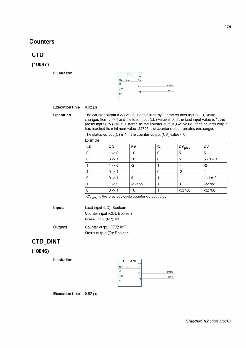
275
Counters
CTD(10047)
Illustration
Execution time 0.92 µs
Operation The counter output (CV) value is decreased by 1 if the counter input (CD) value changes from 0 -> 1 and the load input (LD) value is 0. If the load input value is 1, the preset input (PV) value is stored as the counter output (CV) value. If the counter output has reached its minimum value -32768, the counter output remains unchanged.The status output (Q) is 1 if the counter output (CV) value < 0.Example:
Inputs Load input (LD): BooleanCounter input (CD): BooleanPreset input (PV): INT
Outputs Counter output (CV): INTStatus output (Q): Boolean
CTD_DINT(10046)
Illustration
Execution time 0.92 µs
CTD93
TLA1 1 msec (1)
LD
>CD
PV
CVCV(93)
QQ(93)
LD CD PV Q CVprev CV0 1 -> 0 10 0 5 5
0 0 -> 1 10 0 5 5 - 1 = 4
1 1 -> 0 -2 1 4 -2
1 0 -> 1 1 0 -2 1
0 0 -> 1 5 1 1 1 -1 = 0
1 1 -> 0 -32768 1 0 -32768
0 0 -> 1 10 1 -32768 -32768
CVprev is the previous cycle counter output value.
CTD_DINT94
TLA1 1 msec (1)
LD
>CD
PV
CVCV(94)
QQ(94)
Standard function blocks
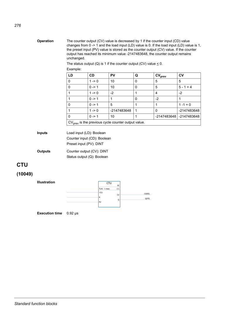
276
Operation The counter output (CV) value is decreased by 1 if the counter input (CD) value changes from 0 -> 1 and the load input (LD) value is 0. If the load input (LD) value is 1, the preset input (PV) value is stored as the counter output (CV) value. If the counter output has reached its minimum value -2147483648, the counter output remains unchanged.The status output (Q) is 1 if the counter output (CV) value < 0.Example:
Inputs Load input (LD): BooleanCounter input (CD): BooleanPreset input (PV): DINT
Outputs Counter output (CV): DINTStatus output (Q): Boolean
CTU(10049)
Illustration
Execution time 0.92 µs
LD CD PV Q CVprev CV0 1 -> 0 10 0 5 5
0 0 -> 1 10 0 5 5 - 1 = 4
1 1 -> 0 -2 1 4 -2
1 0 -> 1 1 0 -2 1
0 0 -> 1 5 1 1 1 -1 = 0
1 1 -> 0 -2147483648 1 0 -2147483648
0 0 -> 1 10 1 -2147483648 -2147483648
CVprev is the previous cycle counter output value.
CTU95
TLA1 1 msec (1)
>CU
R
PV
CVCV(95)
QQ(95)
Standard function blocks
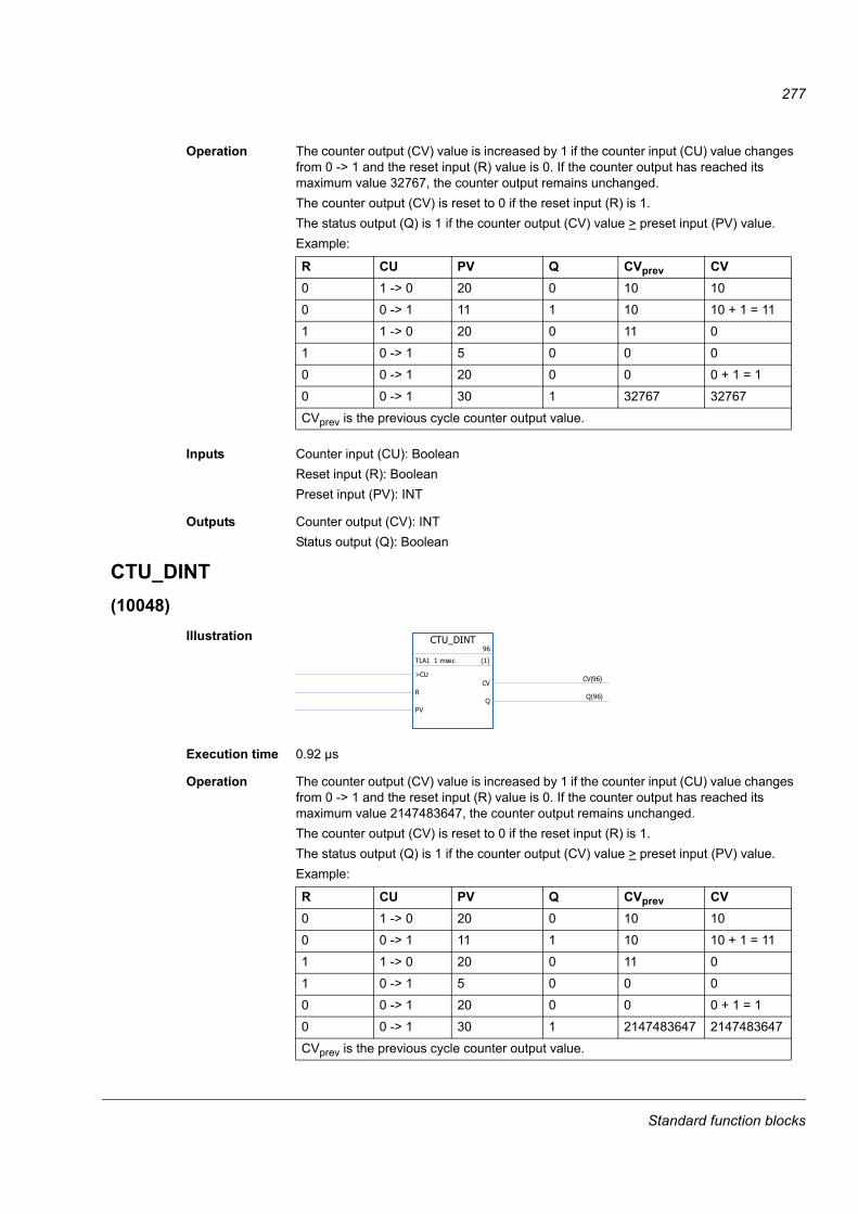
277
Operation The counter output (CV) value is increased by 1 if the counter input (CU) value changes from 0 -> 1 and the reset input (R) value is 0. If the counter output has reached its maximum value 32767, the counter output remains unchanged.The counter output (CV) is reset to 0 if the reset input (R) is 1.The status output (Q) is 1 if the counter output (CV) value > preset input (PV) value.Example:
Inputs Counter input (CU): BooleanReset input (R): BooleanPreset input (PV): INT
Outputs Counter output (CV): INTStatus output (Q): Boolean
CTU_DINT(10048)
Illustration
Execution time 0.92 µs
Operation The counter output (CV) value is increased by 1 if the counter input (CU) value changes from 0 -> 1 and the reset input (R) value is 0. If the counter output has reached its maximum value 2147483647, the counter output remains unchanged.The counter output (CV) is reset to 0 if the reset input (R) is 1.The status output (Q) is 1 if the counter output (CV) value > preset input (PV) value.Example:
R CU PV Q CVprev CV0 1 -> 0 20 0 10 10
0 0 -> 1 11 1 10 10 + 1 = 11
1 1 -> 0 20 0 11 0
1 0 -> 1 5 0 0 0
0 0 -> 1 20 0 0 0 + 1 = 1
0 0 -> 1 30 1 32767 32767
CVprev is the previous cycle counter output value.
CTU_DINT96
TLA1 1 msec (1)
>CU
R
PV
CVCV(96)
QQ(96)
R CU PV Q CVprev CV0 1 -> 0 20 0 10 10
0 0 -> 1 11 1 10 10 + 1 = 11
1 1 -> 0 20 0 11 0
1 0 -> 1 5 0 0 0
0 0 -> 1 20 0 0 0 + 1 = 1
0 0 -> 1 30 1 2147483647 2147483647
CVprev is the previous cycle counter output value.
Standard function blocks
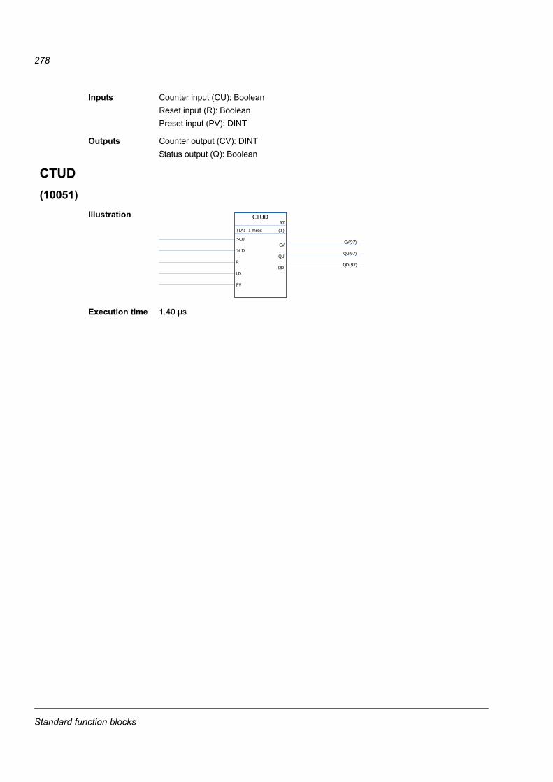
278
Inputs Counter input (CU): BooleanReset input (R): BooleanPreset input (PV): DINT
Outputs Counter output (CV): DINTStatus output (Q): Boolean
CTUD(10051)
Illustration
Execution time 1.40 µs
CTUD97
TLA1 1 msec (1)
>CU
>CD
R
LD
PV
CVCV(97)
QUQU(97)
QDQD(97)
Standard function blocks

279
Operation The counter output (CV) value is increased by 1 if the counter input (CU) value changes from 0 -> 1 and the reset input (R) is 0 and the load input (LD) is 0.The counter output (CV) value is decreased by 1 if the counter input (CD) changes from 0 -> 1 and the load input (LD) is 0 and the reset input (R) is 0.If the load input (LD) is 1, the preset input (PV) value is stored as the counter output (CV) value.The counter output (CV) is reset to 0 if the reset input (R) is 1.If the counter output has reached its minimum or maximum value, -32768 or +32767, the counter output remains unchanged until it is reset (R) or until the load input (LD) is set to 1.The up counter status output (QU) is 1 if the counter output (CV) value > preset input (PV) value.The down counter status output (QD) is 1 if the counter output (CV) value < 0.Example:
Inputs Up counter input (CU): BooleanDown counter input (CD): BooleanReset input (R): BooleanLoad input (LD): BooleanPreset input (PV): INT
Outputs Counter output (CV): INTUp counter status output (QU): BooleanDown counter status output (QD): Boolean
CU CD R LD PV QU QD CVprev CV0 -> 0 0 -> 0 0 0 2 0 1 0 0
0 -> 0 0 -> 0 0 1 2 1 0 0 2
0 -> 0 0 -> 0 1 0 2 0 1 2 0
0 -> 0 0 -> 0 1 1 2 0 1 0 0
0 -> 0 0 -> 1 0 0 2 0 1 0 0 - 1 = -1
0 -> 0 1 -> 1 0 1 2 1 0 -1 2
0 -> 0 1 -> 1 1 0 2 0 1 2 0
0 -> 0 1 -> 1 1 1 2 0 1 0 0
0 -> 1 1 -> 0 0 0 2 0 0 0 0 + 1 = 1
1 -> 1 0 -> 0 0 1 2 1 0 1 2
1 -> 1 0 -> 0 1 0 2 0 1 2 0
1 -> 1 0 -> 0 1 1 2 0 1 0 0
1 -> 1 0 -> 1 0 0 2 0 1 0 0 - 1 = -1
1 -> 1 1 -> 1 0 1 2 1 0 -1 2
1 -> 1 1 -> 1 1 0 2 0 1 2 0
1 -> 1 1 -> 1 1 1 2 0 1 0 0
CVprev is the previous cycle counter output value.
Standard function blocks
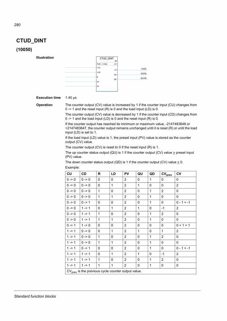
280
CTUD_DINT(10050)
Illustration
Execution time 1.40 µs
Operation The counter output (CV) value is increased by 1 if the counter input (CU) changes from 0 -> 1 and the reset input (R) is 0 and the load input (LD) is 0.The counter output (CV) value is decreased by 1 if the counter input (CD) changes from 0 -> 1 and the load input (LD) is 0 and the reset input (R) is 0.If the counter output has reached its minimum or maximum value, -2147483648 or +2147483647, the counter output remains unchanged until it is reset (R) or until the load input (LD) is set to 1.If the load input (LD) value is 1, the preset input (PV) value is stored as the counter output (CV) value.The counter output (CV) is reset to 0 if the reset input (R) is 1.The up counter status output (QU) is 1 if the counter output (CV) value > preset input (PV) value.The down counter status output (QD) is 1 if the counter output (CV) value < 0.Example:
CTUD_DINT98
TLA1 1 msec (1)
>CU
>CD
R
LD
PV
CVCV(98)
QUQU(98)
QDQD(98)
CU CD R LD PV QU QD CVprev CV0 -> 0 0 -> 0 0 0 2 0 1 0 0
0 -> 0 0 -> 0 0 1 2 1 0 0 2
0 -> 0 0 -> 0 1 0 2 0 1 2 0
0 -> 0 0 -> 0 1 1 2 0 1 0 0
0 -> 0 0 -> 1 0 0 2 0 1 0 0 - 1 = -1
0 -> 0 1 -> 1 0 1 2 1 0 -1 2
0 -> 0 1 -> 1 1 0 2 0 1 2 0
0 -> 0 1 -> 1 1 1 2 0 1 0 0
0 -> 1 1 -> 0 0 0 2 0 0 0 0 + 1 = 1
1 -> 1 0 -> 0 0 1 2 1 0 1 2
1 -> 1 0 -> 0 1 0 2 0 1 2 0
1 -> 1 0 -> 0 1 1 2 0 1 0 0
1 -> 1 0 -> 1 0 0 2 0 1 0 0 - 1 = -1
1 -> 1 1 -> 1 0 1 2 1 0 -1 2
1 -> 1 1 -> 1 1 0 2 0 1 2 0
1 -> 1 1 -> 1 1 1 2 0 1 0 0
CVprev is the previous cycle counter output value.
Standard function blocks
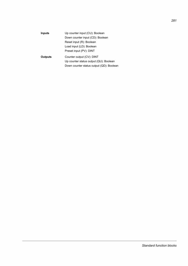
281
Inputs Up counter input (CU): BooleanDown counter input (CD): BooleanReset input (R): BooleanLoad input (LD): BooleanPreset input (PV): DINT
Outputs Counter output (CV): DINTUp counter status output (QU): BooleanDown counter status output (QD): Boolean
Standard function blocks
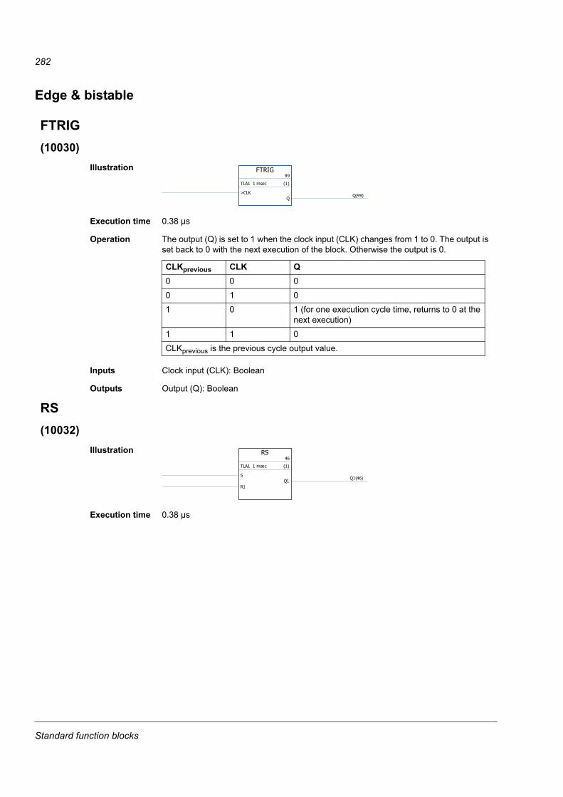
282
Edge & bistable
FTRIG(10030)
Illustration
Execution time 0.38 µs
Operation The output (Q) is set to 1 when the clock input (CLK) changes from 1 to 0. The output is set back to 0 with the next execution of the block. Otherwise the output is 0.
Inputs Clock input (CLK): Boolean
Outputs Output (Q): Boolean
RS(10032)
Illustration
Execution time 0.38 µs
FTRIG99
TLA1 1 msec (1)
>CLKQ
Q(99)
CLKprevious CLK Q0 0 0
0 1 0
1 0 1 (for one execution cycle time, returns to 0 at the next execution)
1 1 0
CLKprevious is the previous cycle output value.
RS46
TLA1 1 msec (1)
S
R1Q1
Q1(46)
Standard function blocks
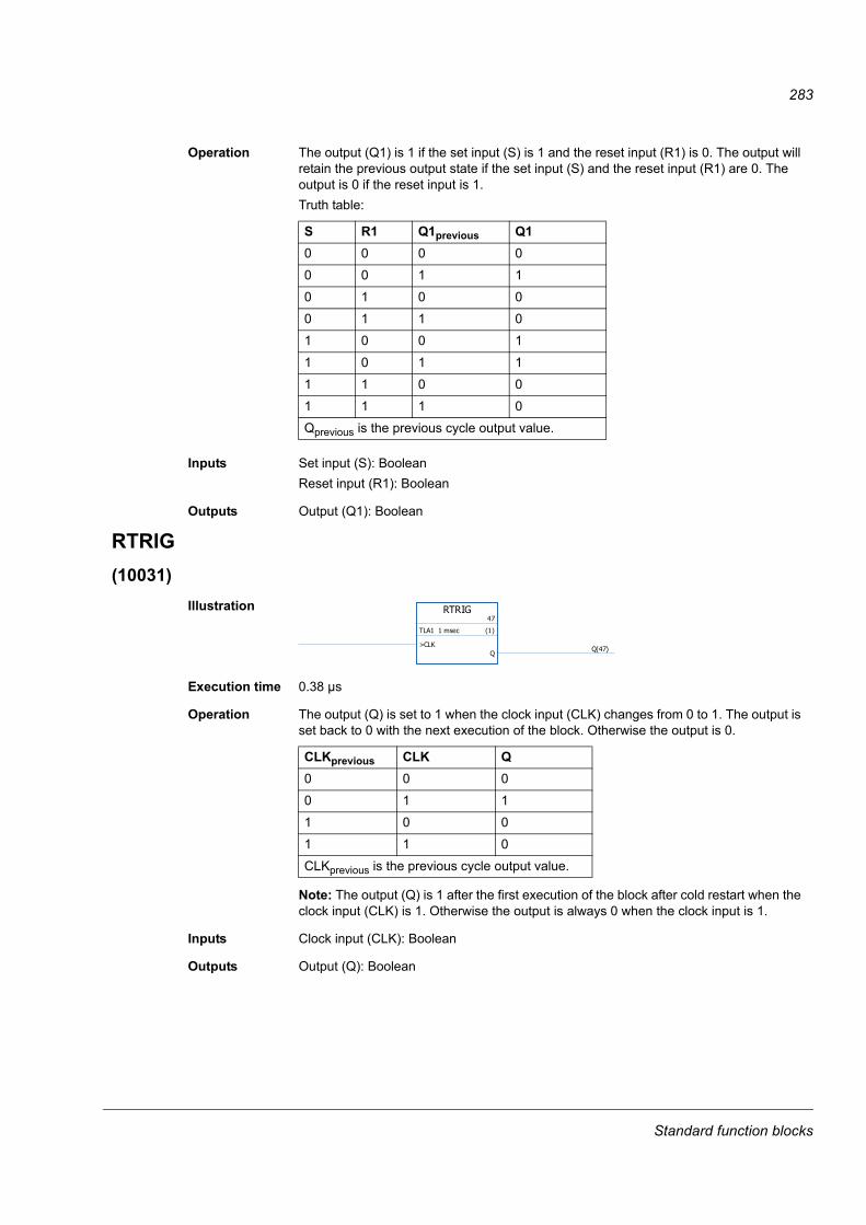
283
Operation The output (Q1) is 1 if the set input (S) is 1 and the reset input (R1) is 0. The output will retain the previous output state if the set input (S) and the reset input (R1) are 0. The output is 0 if the reset input is 1.Truth table:
Inputs Set input (S): BooleanReset input (R1): Boolean
Outputs Output (Q1): Boolean
RTRIG(10031)
Illustration
Execution time 0.38 µs
Operation The output (Q) is set to 1 when the clock input (CLK) changes from 0 to 1. The output is set back to 0 with the next execution of the block. Otherwise the output is 0.
Note: The output (Q) is 1 after the first execution of the block after cold restart when the clock input (CLK) is 1. Otherwise the output is always 0 when the clock input is 1.
Inputs Clock input (CLK): Boolean
Outputs Output (Q): Boolean
S R1 Q1previous Q10 0 0 0
0 0 1 1
0 1 0 0
0 1 1 0
1 0 0 1
1 0 1 1
1 1 0 0
1 1 1 0
Qprevious is the previous cycle output value.
RTRIG47
TLA1 1 msec (1)
>CLKQ
Q(47)
CLKprevious CLK Q0 0 0
0 1 1
1 0 0
1 1 0
CLKprevious is the previous cycle output value.
Standard function blocks

284
SR(10033)
Illustration
Execution time 0.38 µs
Operation The output (Q1) is 1 if the set input (S1) is 1. The output will retain the previous output state if the set input (S1) and the reset input (R) are 0. The output is 0 if the set input is 0 and the reset input is 1.Truth table:
Inputs Set input (S1): BooleanReset input (R): Boolean
Outputs Output (Q1): Boolean
SR48
TLA1 1 msec (1)
S1
RQ1
Q1(48)
S1 R Q1previous Q10 0 0 0
0 0 1 1
0 1 0 0
0 1 1 0
1 0 0 1
1 0 1 1
1 1 0 1
1 1 1 1
Q1previous is the previous cycle output value.
Standard function blocks
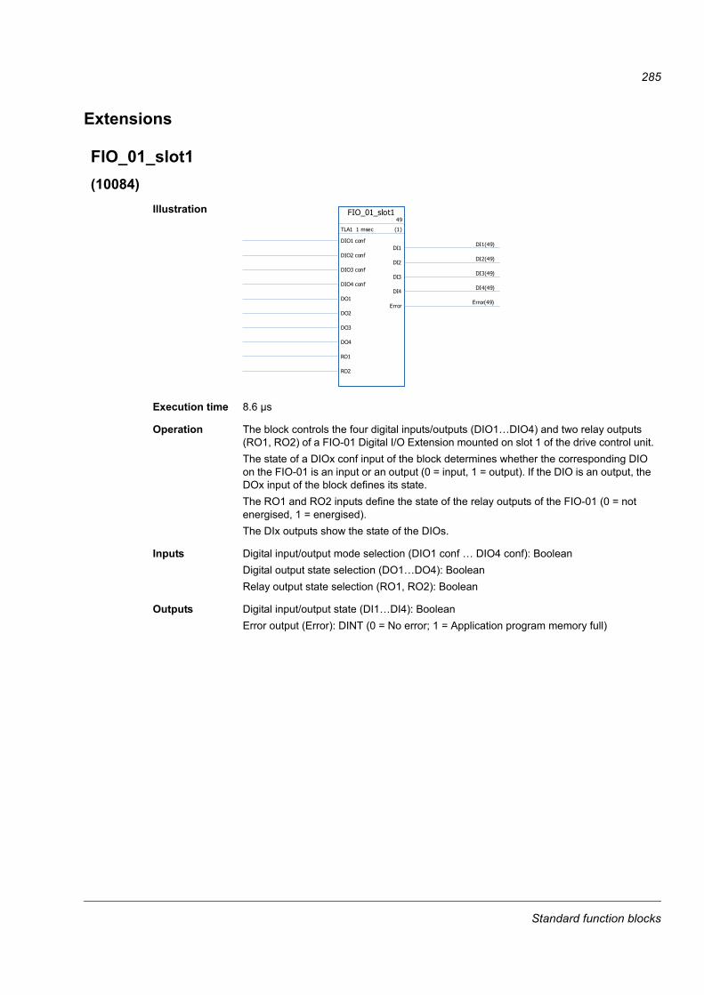
285
Extensions
FIO_01_slot1(10084)
Illustration
Execution time 8.6 µs
Operation The block controls the four digital inputs/outputs (DIO1…DIO4) and two relay outputs (RO1, RO2) of a FIO-01 Digital I/O Extension mounted on slot 1 of the drive control unit.The state of a DIOx conf input of the block determines whether the corresponding DIO on the FIO-01 is an input or an output (0 = input, 1 = output). If the DIO is an output, the DOx input of the block defines its state.The RO1 and RO2 inputs define the state of the relay outputs of the FIO-01 (0 = not energised, 1 = energised).The DIx outputs show the state of the DIOs.
Inputs Digital input/output mode selection (DIO1 conf … DIO4 conf): BooleanDigital output state selection (DO1…DO4): BooleanRelay output state selection (RO1, RO2): Boolean
Outputs Digital input/output state (DI1…DI4): BooleanError output (Error): DINT (0 = No error; 1 = Application program memory full)
FIO_01_slot149
TLA1 1 msec (1)
DIO1 conf
DIO2 conf
DIO3 conf
DIO4 conf
DO1
DO2
DO3
DO4
RO1
RO2
DI1DI1(49)
DI2DI2(49)
DI3DI3(49)
DI4DI4(49)
ErrorError(49)
Standard function blocks
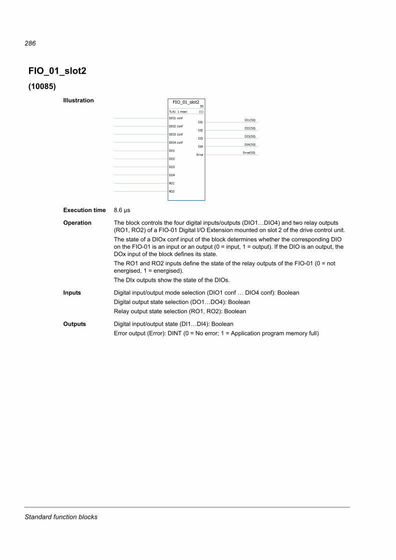
286
FIO_01_slot2(10085)
Illustration
Execution time 8.6 µs
Operation The block controls the four digital inputs/outputs (DIO1…DIO4) and two relay outputs (RO1, RO2) of a FIO-01 Digital I/O Extension mounted on slot 2 of the drive control unit.The state of a DIOx conf input of the block determines whether the corresponding DIO on the FIO-01 is an input or an output (0 = input, 1 = output). If the DIO is an output, the DOx input of the block defines its state.The RO1 and RO2 inputs define the state of the relay outputs of the FIO-01 (0 = not energised, 1 = energised).The DIx outputs show the state of the DIOs.
Inputs Digital input/output mode selection (DIO1 conf … DIO4 conf): BooleanDigital output state selection (DO1…DO4): BooleanRelay output state selection (RO1, RO2): Boolean
Outputs Digital input/output state (DI1…DI4): BooleanError output (Error): DINT (0 = No error; 1 = Application program memory full)
FIO_01_slot250
TLA1 1 msec (1)
DIO1 conf
DIO2 conf
DIO3 conf
DIO4 conf
DO1
DO2
DO3
DO4
RO1
RO2
DI1DI1(50)
DI2DI2(50)
DI3DI3(50)
DI4DI4(50)
ErrorError(50)
Standard function blocks
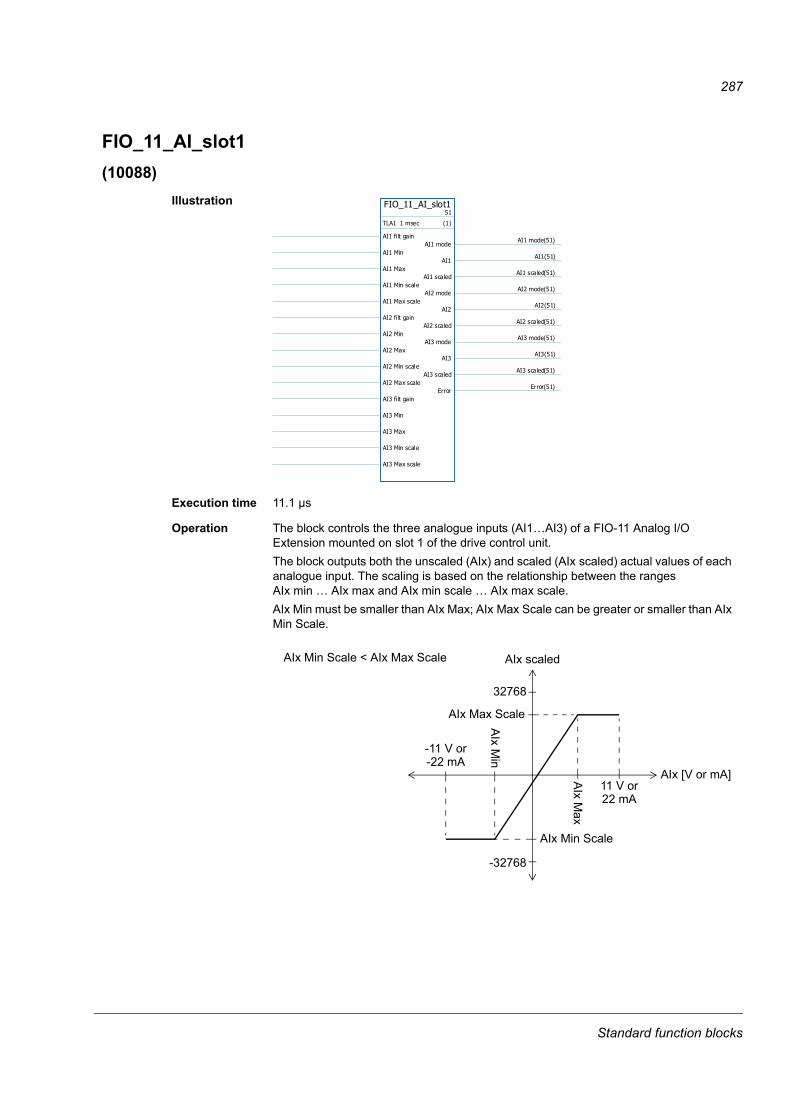
287
FIO_11_AI_slot1(10088)
Illustration
Execution time 11.1 µs
Operation The block controls the three analogue inputs (AI1…AI3) of a FIO-11 Analog I/O Extension mounted on slot 1 of the drive control unit.The block outputs both the unscaled (AIx) and scaled (AIx scaled) actual values of each analogue input. The scaling is based on the relationship between the ranges AIx min … AIx max and AIx min scale … AIx max scale.AIx Min must be smaller than AIx Max; AIx Max Scale can be greater or smaller than AIx Min Scale.
FIO_11_AI_slot151
TLA1 1 msec (1)
AI1 filt gain
AI1 Min
AI1 Max
AI1 Min scale
AI1 Max scale
AI2 filt gain
AI2 Min
AI2 Max
AI2 Min scale
AI2 Max scale
AI3 filt gain
AI3 Min
AI3 Max
AI3 Min scale
AI3 Max scale
AI1 modeAI1 mode(51)
AI1AI1(51)
AI1 scaledAI1 scaled(51)
AI2 modeAI2 mode(51)
AI2AI2(51)
AI2 scaledAI2 scaled(51)
AI3 modeAI3 mode(51)
AI3AI3(51)
AI3 scaledAI3 scaled(51)
ErrorError(51)
AIx scaled
32768
AIx [V or mA]11 V or
-11 V or
AIx Max
AIx M
in
AIx Max Scale
AIx Min Scale
-22 mA
22 mA
AIx Min Scale < AIx Max Scale
-32768
Standard function blocks

288
The AIx filt gain inputs determine a filtering time for each input as follows:
The AIx mode outputs show whether the corresponding input is voltage (0) or current (1). The voltage/current selection is made using the hardware switches on the FIO-11.
Inputs Analogue input filter gain selection (AI1 filt gain … AI3 filt gain): INTMinimum value of input signal (AI1 Min … AI3 Min): REAL (> -11 V or -22 mA)Maximum value of input signal (AI1 Max … AI3 Max): REAL (< 11 V or 22 mA)Minimum value of scaled output signal (AI1 Min scale … AI3 Min scale): REALMaximum value of scaled output signal (AI1 Max scale … AI3 Max scale): REAL
Outputs Analogue input mode (voltage or current) (AI1 mode … AI3 mode): BooleanValue of analogue input (AI1 … AI3): REALScaled value of analogue input (AI1 scaled … AI3 scaled): REALError output (Error): DINT (0 = No error; 1 = Application program memory full)
AIx scaled
32768
AIx [V or mA]
11 V or
-11 V or
AIx M
ax
AIx M
in
AIx Min Scale
AIx Max Scale
-22 mA
22 mA
AIx Min Scale > AIx Max Scale
-32768
AIx filt gain Filtering time Notes0 No filtering
1 125 µs Recommended setting
2 250 µs
3 500 µs
4 1 ms
5 2 ms
6 4 ms
7 7.9375 ms
Standard function blocks
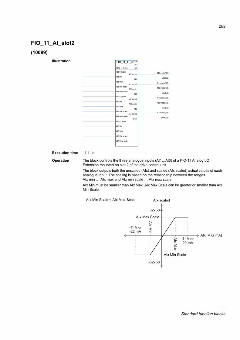
289
FIO_11_AI_slot2(10089)
Illustration
Execution time 11.1 µs
Operation The block controls the three analogue inputs (AI1…AI3) of a FIO-11 Analog I/O Extension mounted on slot 2 of the drive control unit.The block outputs both the unscaled (AIx) and scaled (AIx scaled) actual values of each analogue input. The scaling is based on the relationship between the ranges AIx min … AIx max and AIx min scale … AIx max scale.AIx Min must be smaller than AIx Max; AIx Max Scale can be greater or smaller than AIx Min Scale.
FIO_11_AI_slot252
TLA1 1 msec (1)
AI1 filt gain
AI1 Min
AI1 Max
AI1 Min scale
AI1 Max scale
AI2 filt gain
AI2 Min
AI2 Max
AI2 Min scale
AI2 Max scale
AI3 filt gain
AI3 Min
AI3 Max
AI3 Min scale
AI3 Max scale
AI1 modeAI1 mode(52)
AI1AI1(52)
AI1 scaledAI1 scaled(52)
AI2 modeAI2 mode(52)
AI2AI2(52)
AI2 scaledAI2 scaled(52)
AI3 modeAI3 mode(52)
AI3AI3(52)
AI3 scaledAI3 scaled(52)
ErrorError(52)
AIx scaled
32768
AIx [V or mA]11 V or
-11 V or
AIx Max
AIx M
in
AIx Max Scale
AIx Min Scale
-22 mA
22 mA
AIx Min Scale < AIx Max Scale
-32768
Standard function blocks
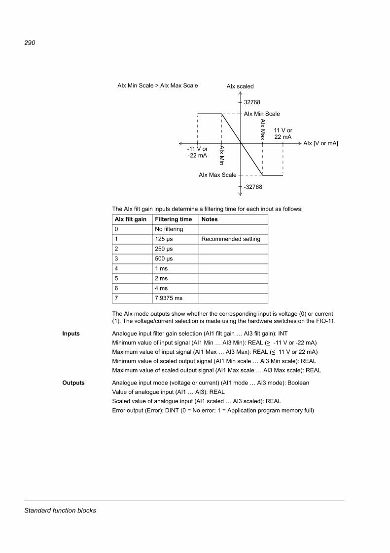
290
The AIx filt gain inputs determine a filtering time for each input as follows:
The AIx mode outputs show whether the corresponding input is voltage (0) or current (1). The voltage/current selection is made using the hardware switches on the FIO-11.
Inputs Analogue input filter gain selection (AI1 filt gain … AI3 filt gain): INTMinimum value of input signal (AI1 Min … AI3 Min): REAL (> -11 V or -22 mA)Maximum value of input signal (AI1 Max … AI3 Max): REAL (< 11 V or 22 mA)Minimum value of scaled output signal (AI1 Min scale … AI3 Min scale): REALMaximum value of scaled output signal (AI1 Max scale … AI3 Max scale): REAL
Outputs Analogue input mode (voltage or current) (AI1 mode … AI3 mode): BooleanValue of analogue input (AI1 … AI3): REALScaled value of analogue input (AI1 scaled … AI3 scaled): REALError output (Error): DINT (0 = No error; 1 = Application program memory full)
AIx scaled
32768
AIx [V or mA]
11 V or
-11 V or
AIx M
ax
AIx M
in
AIx Min Scale
AIx Max Scale
-22 mA
22 mA
AIx Min Scale > AIx Max Scale
-32768
AIx filt gain Filtering time Notes0 No filtering
1 125 µs Recommended setting
2 250 µs
3 500 µs
4 1 ms
5 2 ms
6 4 ms
7 7.9375 ms
Standard function blocks
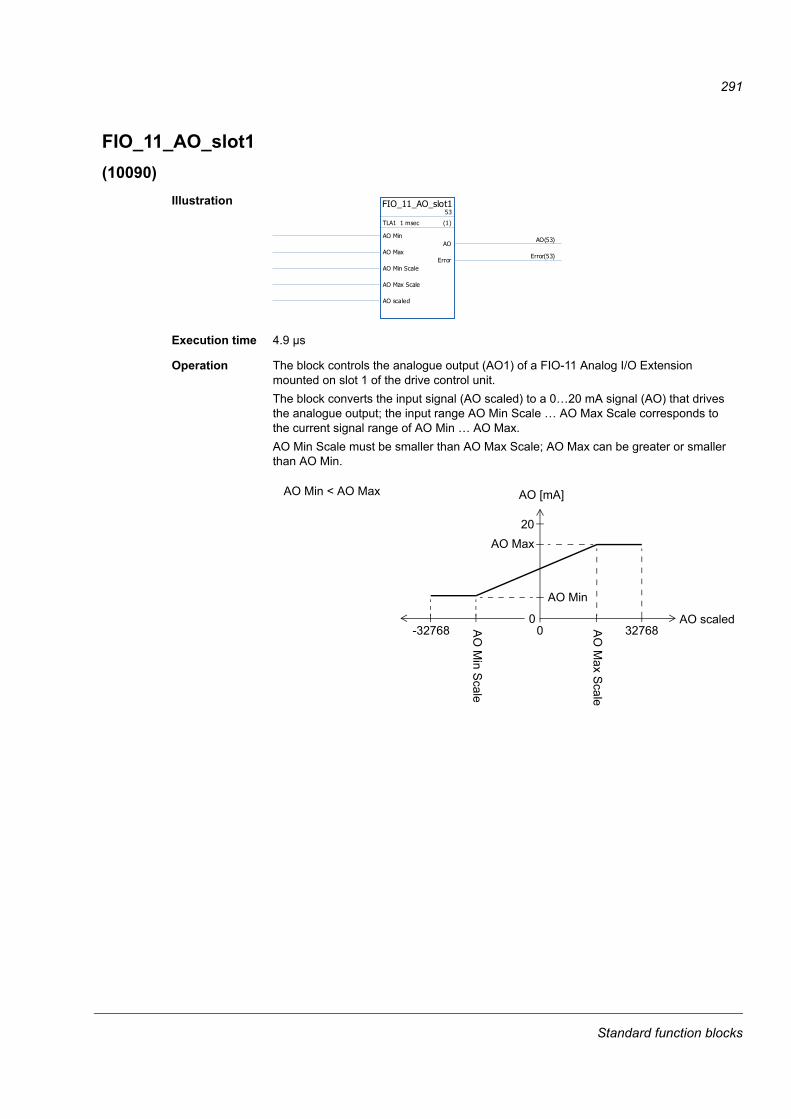
291
FIO_11_AO_slot1(10090)
Illustration
Execution time 4.9 µs
Operation The block controls the analogue output (AO1) of a FIO-11 Analog I/O Extension mounted on slot 1 of the drive control unit.The block converts the input signal (AO scaled) to a 0…20 mA signal (AO) that drives the analogue output; the input range AO Min Scale … AO Max Scale corresponds to the current signal range of AO Min … AO Max.AO Min Scale must be smaller than AO Max Scale; AO Max can be greater or smaller than AO Min.
FIO_11_AO_slot153
TLA1 1 msec (1)
AO Min
AO Max
AO Min Scale
AO Max Scale
AO scaled
AOAO(53)
ErrorError(53)
AO [mA]
0
20
AO scaled32768-32768 0 A
O M
ax Scale
AO
Min S
cale
AO Max
AO Min
AO Min < AO Max
Standard function blocks
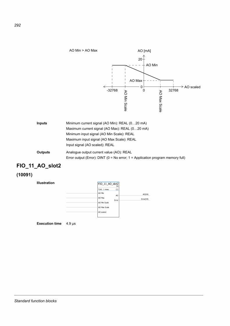
292
Inputs Minimum current signal (AO Min): REAL (0…20 mA)Maximum current signal (AO Max): REAL (0…20 mA)Minimum input signal (AO Min Scale): REALMaximum input signal (AO Max Scale): REALInput signal (AO scaled): REAL
Outputs Analogue output current value (AO): REALError output (Error): DINT (0 = No error; 1 = Application program memory full)
FIO_11_AO_slot2(10091)
Illustration
Execution time 4.9 µs
AO Min > AO Max AO [mA]
0
20
AO scaled32768-32768 0 A
O M
ax Scale
AO
Min S
cale
AO Max
AO Min
FIO_11_AO_slot254
TLA1 1 msec (1)
AO Min
AO Max
AO Min Scale
AO Max Scale
AO scaled
AOAO(54)
ErrorError(54)
Standard function blocks

293
Operation The block controls the analogue output (AO1) of a FIO-11 Analog I/O Extension mounted on slot 2 of the drive control unit.The block converts the input signal (AO scaled) to a 0…20 mA signal (AO) that drives the analogue output; the input range AO Min Scale … AO Max Scale corresponds to the current signal range of AO Min … AO Max.AO Min Scale must be smaller than AO Max Scale; AO Max can be greater or smaller than AO Min.
Inputs Minimum current signal (AO Min): REAL (0…20 mA)Maximum current signal (AO Max): REAL (0…20 mA)Minimum input signal (AO Min Scale): REALMaximum input signal (AO Max Scale): REALInput signal (AO scaled): REAL
Outputs Analogue output current value (AO): REALError output (Error): DINT (0 = No error; 1 = Application program memory full)
AO [mA]
0
20
AO scaled32768-32768 0 A
O M
ax Scale
AO
Min S
caleAO Max
AO Min
AO Min < AO Max
AO Min > AO Max AO [mA]
0
20
AO scaled32768-32768 0 A
O M
ax Scale
AO
Min S
cale
AO Max
AO Min
Standard function blocks

294
FIO_11_DIO_slot1(10086)
Illustration
Execution time 6.0 µs
Operation The block controls the two digital inputs/outputs (DIO1, DIO2) of a FIO-11 Digital I/O Extension mounted on slot 1 of the drive control unit.The state of a DIOx conf input of the block determines whether the corresponding DIO on the FIO-11 is an input or an output (0 = input, 1 = output). If the DIO is an output, the DOx input of the block defines its state.The DIx outputs show the state of the DIOs.The DIx filt gain inputs determine a filtering time for each input as follows:
Inputs Digital input/output mode selection (DIO1 conf, DIO2 conf): BooleanDigital output state selection (DO1, DO2): BooleanDigital input filter gain selection (DI1 filt gain, DI2 filt gain): INT
Outputs Digital input/output state (DI1, DI2): BooleanError output (Error): DINT (0 = No error; 1 = Application program memory full)
FIO_11_DIO_slot2(10087)
Illustration
Execution time 6.0 µs
FIO_11_DIO_slot155
TLA1 1 msec (1)
DIO1 conf
DIO2 conf
DO1
DO2
DI1 filt gain
DI2 filt gain
DI1DI1(55)
DI2DI2(55)
ErrorError(55)
DIx filt gain Filtering time0 7.5 µs
1 195 µs
2 780 µs
3 4.680 ms
FIO_11_DIO_slot256
TLA1 1 msec (1)
DIO1 conf
DIO2 conf
DO1
DO2
DI1 filt gain
DI2 filt gain
DI1DI1(56)
DI2DI2(56)
ErrorError(56)
Standard function blocks
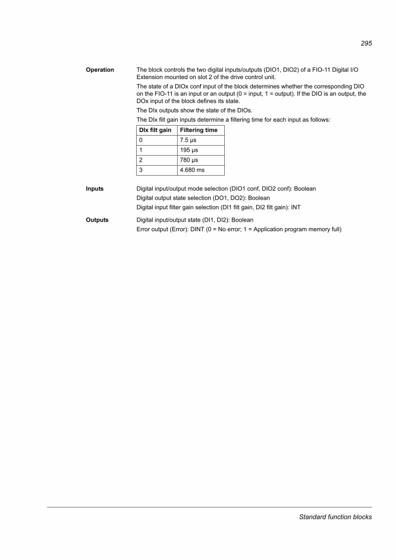
295
Operation The block controls the two digital inputs/outputs (DIO1, DIO2) of a FIO-11 Digital I/O Extension mounted on slot 2 of the drive control unit.The state of a DIOx conf input of the block determines whether the corresponding DIO on the FIO-11 is an input or an output (0 = input, 1 = output). If the DIO is an output, the DOx input of the block defines its state.The DIx outputs show the state of the DIOs.The DIx filt gain inputs determine a filtering time for each input as follows:
Inputs Digital input/output mode selection (DIO1 conf, DIO2 conf): BooleanDigital output state selection (DO1, DO2): BooleanDigital input filter gain selection (DI1 filt gain, DI2 filt gain): INT
Outputs Digital input/output state (DI1, DI2): BooleanError output (Error): DINT (0 = No error; 1 = Application program memory full)
DIx filt gain Filtering time0 7.5 µs
1 195 µs
2 780 µs
3 4.680 ms
Standard function blocks
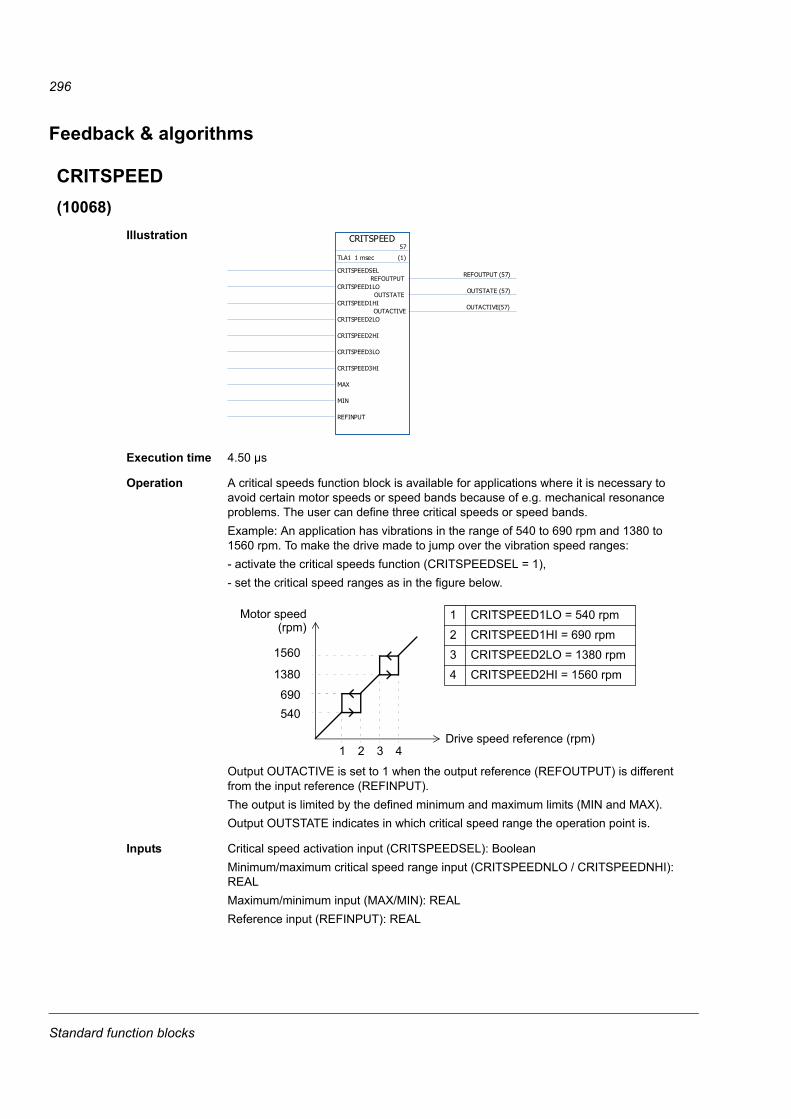
296
Feedback & algorithms
CRITSPEED(10068)
Illustration
Execution time 4.50 µs
Operation A critical speeds function block is available for applications where it is necessary to avoid certain motor speeds or speed bands because of e.g. mechanical resonance problems. The user can define three critical speeds or speed bands.Example: An application has vibrations in the range of 540 to 690 rpm and 1380 to 1560 rpm. To make the drive made to jump over the vibration speed ranges:- activate the critical speeds function (CRITSPEEDSEL = 1),- set the critical speed ranges as in the figure below.
Output OUTACTIVE is set to 1 when the output reference (REFOUTPUT) is different from the input reference (REFINPUT).The output is limited by the defined minimum and maximum limits (MIN and MAX).Output OUTSTATE indicates in which critical speed range the operation point is.
Inputs Critical speed activation input (CRITSPEEDSEL): BooleanMinimum/maximum critical speed range input (CRITSPEEDNLO / CRITSPEEDNHI): REALMaximum/minimum input (MAX/MIN): REALReference input (REFINPUT): REAL
CRITSPEED57
TLA1 1 msec (1)
CRITSPEEDSEL
CRITSPEED1LO
CRITSPEED1HI
CRITSPEED2LO
CRITSPEED2HI
CRITSPEED3LO
CRITSPEED3HI
MAX
MIN
REFINPUT
REFOUTPUT REFOUTPUT (57)
OUTSTATE OUTSTATE (57)
OUTACTIVEOUTACTIVE(57)
Drive speed reference (rpm)
540690
1380
1560
Motor speed 1 CRITSPEED1LO = 540 rpm
2 CRITSPEED1HI = 690 rpm
3 CRITSPEED2LO = 1380 rpm
4 CRITSPEED2HI = 1560 rpm
1 2 3 4
(rpm)
Standard function blocks
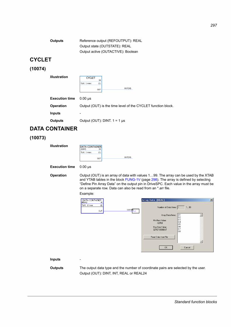
297
Outputs Reference output (REFOUTPUT): REALOutput state (OUTSTATE): REALOutput active (OUTACTIVE): Boolean
CYCLET(10074)
Illustration
Execution time 0.00 µs
Operation Output (OUT) is the time level of the CYCLET function block.
Inputs -
Outputs Output (OUT): DINT. 1 = 1 µs
DATA CONTAINER(10073)
Illustration
Execution time 0.00 µs
Operation Output (OUT) is an array of data with values 1…99. The array can be used by the XTAB and YTAB tables in the block FUNG-1V (page 298). The array is defined by selecting “Define Pin Array Data” on the output pin in DriveSPC. Each value in the array must be on a separate row. Data can also be read from an *.arr file.Example:
Inputs -
Outputs The output data type and the number of coordinate pairs are selected by the user.Output (OUT): DINT, INT, REAL or REAL24
CYCLET58
TLA1 1 msec (1)
OUTOUT(58)
DATA CONTAINER(DINT) 59
TLA1 1 msec (1)
OUTOUT(59)
Standard function blocks
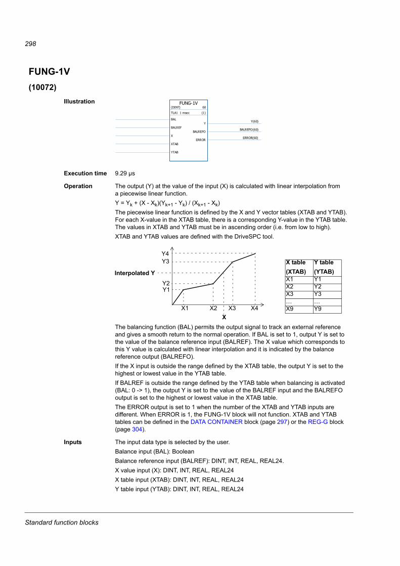
298
FUNG-1V(10072)
Illustration
Execution time 9.29 µs
Operation The output (Y) at the value of the input (X) is calculated with linear interpolation from a piecewise linear function.Y = Yk + (X - Xk)(Yk+1 - Yk) / (Xk+1 - Xk)The piecewise linear function is defined by the X and Y vector tables (XTAB and YTAB). For each X-value in the XTAB table, there is a corresponding Y-value in the YTAB table. The values in XTAB and YTAB must be in ascending order (i.e. from low to high).XTAB and YTAB values are defined with the DriveSPC tool.
The balancing function (BAL) permits the output signal to track an external reference and gives a smooth return to the normal operation. If BAL is set to 1, output Y is set to the value of the balance reference input (BALREF). The X value which corresponds to this Y value is calculated with linear interpolation and it is indicated by the balance reference output (BALREFO).If the X input is outside the range defined by the XTAB table, the output Y is set to the highest or lowest value in the YTAB table.If BALREF is outside the range defined by the YTAB table when balancing is activated (BAL: 0 -> 1), the output Y is set to the value of the BALREF input and the BALREFO output is set to the highest or lowest value in the XTAB table.The ERROR output is set to 1 when the number of the XTAB and YTAB inputs are different. When ERROR is 1, the FUNG-1V block will not function. XTAB and YTAB tables can be defined in the DATA CONTAINER block (page 297) or the REG-G block (page 304).
Inputs The input data type is selected by the user.Balance input (BAL): BooleanBalance reference input (BALREF): DINT, INT, REAL, REAL24.X value input (X): DINT, INT, REAL, REAL24X table input (XTAB): DINT, INT, REAL, REAL24Y table input (YTAB): DINT, INT, REAL, REAL24
FUNG-1V(DINT) 60
TLA1 1 msec (1)
BAL
BALREF
X
XTAB
YTAB
YY(60)
BALREFOBALREFO(60)
ERRORERROR(60)
X1 X2 X3 X4
Y1Y2
Y3Y4
X
Interpolated Y
X table(XTAB)
Y table(YTAB)
X1 Y1X2 Y2X3 Y3… …X9 Y9
Standard function blocks

299
Outputs Y value output (Y): DINT, INT, REAL, REAL24Balance reference output (BALREFO): DINT, INT, REAL, REAL24Error output (ERROR): Boolean
INT(10065)
Illustration
Execution time 4.73 µs
Operation The output (O) is the integrated value of the input (I):O(t) = K/TI (∫ I(t) dt)Where TI is the integration time constant and K is the integration gain.The step response for the integration is:O(t) = K × I(t) × t/TIThe transfer function for the integration is:G(s) = K 1/sTIThe output value is limited according to the defined minimum and maximum limits (OLL and OHL). If the value is below the minimum value, output O = LL is set to 1. If the value exceeds the maximum value, output O = HL is set to 1. The output (O) retains its value when the input signal I(t) = 0. The integration time constant is limited to value 2147483 ms. If the time constant is negative, zero time constant is used.If the ratio between the cycle time and the integration time constant Ts/TI < 1, Ts/TI is set to 1.The integrator is cleared when the reset input (RINT) is set to 1.If BAL is set to 1, output O is set to the value of the input BALREF. When BAL is set back to 0, normal integration operation continues.
Inputs Input (I): REALGain input (K): REALIntegration time constant input (TI): DINT, 0…2147483 msIntegrator reset input (RINT): BooleanBalance input (BAL): BooleanBalance reference input (BALREF): REALOutput high limit input (OHL): REALOutput low limit input (OLL): REAL
INT61
TLA1 1 msec (1)
I
K
TI
RINT
BAL
BALREF
OHL
OLL
OO(61)
O=HLO=HL(61)
O=LLO=LL(61)
Standard function blocks
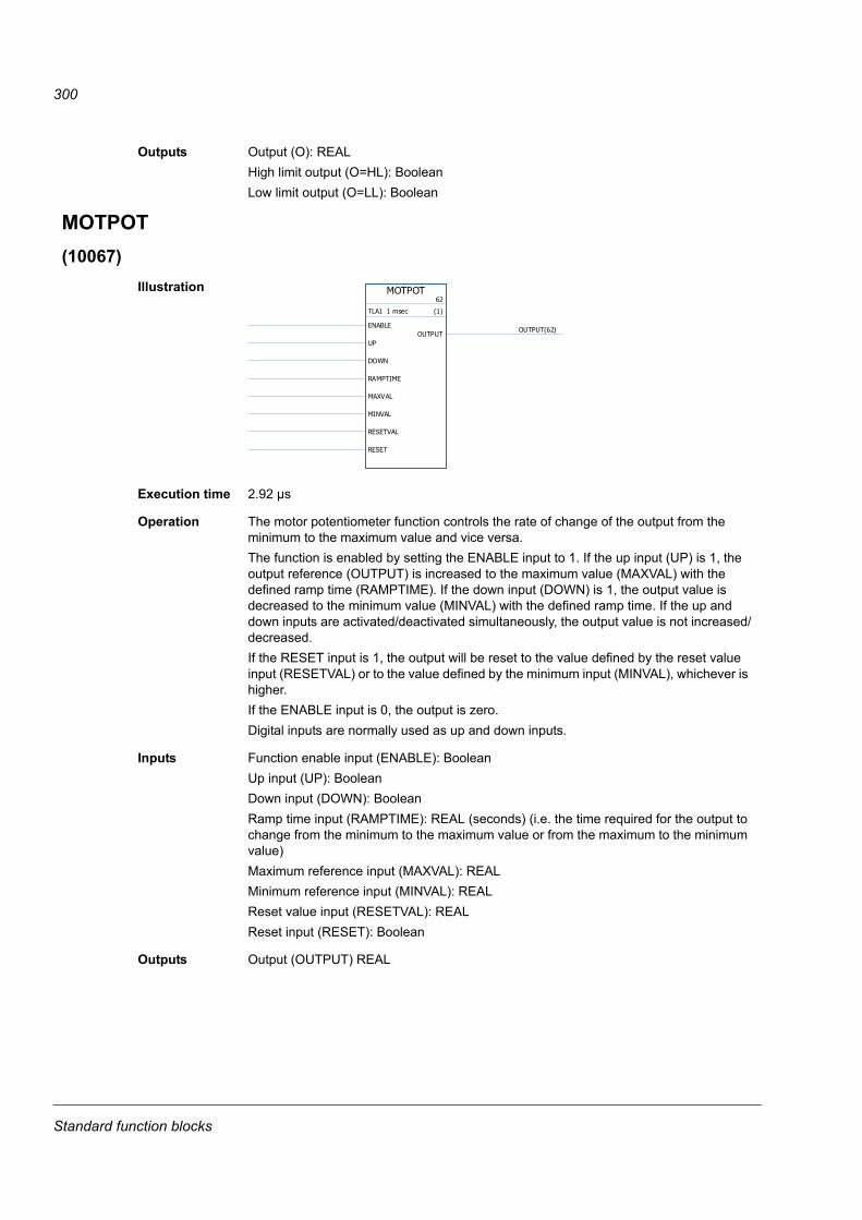
300
Outputs Output (O): REALHigh limit output (O=HL): BooleanLow limit output (O=LL): Boolean
MOTPOT(10067)
Illustration
Execution time 2.92 µs
Operation The motor potentiometer function controls the rate of change of the output from the minimum to the maximum value and vice versa.The function is enabled by setting the ENABLE input to 1. If the up input (UP) is 1, the output reference (OUTPUT) is increased to the maximum value (MAXVAL) with the defined ramp time (RAMPTIME). If the down input (DOWN) is 1, the output value is decreased to the minimum value (MINVAL) with the defined ramp time. If the up and down inputs are activated/deactivated simultaneously, the output value is not increased/decreased.If the RESET input is 1, the output will be reset to the value defined by the reset value input (RESETVAL) or to the value defined by the minimum input (MINVAL), whichever is higher.If the ENABLE input is 0, the output is zero. Digital inputs are normally used as up and down inputs.
Inputs Function enable input (ENABLE): BooleanUp input (UP): BooleanDown input (DOWN): BooleanRamp time input (RAMPTIME): REAL (seconds) (i.e. the time required for the output to change from the minimum to the maximum value or from the maximum to the minimum value)Maximum reference input (MAXVAL): REALMinimum reference input (MINVAL): REALReset value input (RESETVAL): REALReset input (RESET): Boolean
Outputs Output (OUTPUT) REAL
MOTPOT62
TLA1 1 msec (1)
ENABLE
UP
DOWN
RAMPTIME
MAXVAL
MINVAL
RESETVAL
RESET
OUTPUTOUTPUT(62)
Standard function blocks

301
PID(10075)
Illustration
Execution time 15.75 µs
PID63
TLA1 1 msec (1)
IN_act
IN_ref
P
tI
tD
tC
I_reset
BAL
BAL_ref
OHL
OLL
OutOut(63)
DevDev(63)
O=HLO=HL(63)
O=LLO=LL(63)
ERRORERROR(63)
Standard function blocks
302
Operation The PID controller can be used for closed-loop control systems. The controller includes anti-windup correction and output limitation. The PID controller output (Out) before limitation is the sum of the proportional (UP), integral (UI) and derivative (UD) terms:Outunlimited (t) = UP(t) + UI(t) + UD(t)UP(t) = P × Dev(t)UI(t) = P/tI × [∫ Dev(τ)dτ + tC × (Out(t) - Outunlimited(t))]UD(t) = P × tD × d(Dev(t))/dtIntegrator:The integral term can be cleared by setting I_reset to 1. Note that the anti-windup correction is simultaneously disabled. When I_reset is 1, the controller acts as a PD controller.If integration time constant tI is 0, the integral term will not be updated.Smooth return to normal operation is guaranteed after errors or abrupt input value changes. This is achieved by adjusting the integral term so that the output will retain its previous value during these situations.Limitation:The output is limited by the defined minimum and maximum values, OLL and OHL: If the actual value of the output reaches the specified minimum limit, output O=LL is set to 1.If the actual value of the output reaches the specified maximum limit, output O=HL is set to 1.Smooth return to normal operation after limitation is requested if and only if the anti-windup correction is not used, i.e. when tI = 0 or tC = 0.Error codes:Error codes are indicated by the error output (ERROR) as follows
Balancing:The balancing function (BAL) permits the output signal to track an external reference and gives a smooth return to the normal operation. If BAL is set to 1, the output (Out) is set to the value of the balance reference input (BAL_ref). Balance reference is limited by the defined minimum and maximum limits (OLL and OHL).Anti-windup:Anti-windup correction time constant is defined by input tC, which defines the time after which the difference between the unlimited and limited outputs is subtracted from the I-term during limitation. If tC = 0 or tI = 0, anti-windup correction is disabled.
Error code Description1 The minimum limit (OLL) exceeds the maximum limit (OHL).
2 Overflow with Up, Ui, or Ud calculation
Standard function blocks
303
Inputs Actual input (IN_act): REALReference input (IN_ref): REALProportional gain input (P): REALIntegration time constant input (tI): REAL. 1 = 1 msDerivation time constant input (tD): REAL. 1 = 1 msAntiwind-up correction time constant input (tC): IQ6. 1 = 1 msIntegrator reset input (I_reset): BooleanBalance input (BAL): Boolean Balance reference input (BAL_ref): REALOutput high limit input (OHL): REALOutput low limit input (OLL): REAL
Outputs Output (Out): REALDeviation output (Dev): REAL (= actual -reference = IN_act - IN_ref)High limit output (O=HL): BooleanLow limit output (O=LL): BooleanError code output (ERROR): INT32
RAMP(10066)
Illustration
Execution time 4.23 µs
Operation Limits the rate of the change of the signal.The input signal (IN) is connected directly to the output (O) if the input signal does not exceed the defined step change limits (STEP+ and STEP-). If the input signal change exceeds these limits, the output signal change is limited by the maximum step change (STEP+/STEP- depending on the direction of rotation). After this, the output signal is accelerated/decelerated by the defined ramp value (SLOPE+/SLOPE-) per second until the input and output signal values are equal.The output is limited by the defined minimum and maximum values (OLL and OHL). If the actual value of the output falls below the specified minimum limit (OLL), output O=LL is set to 1. If the actual value of the output exceeds the specified maximum limit (OHL), output O=HL is set to 1. If the balancing input (BAL) is set to 1, the output (O) is set to the value of the balance reference input (BAL_ref). Balancing reference is also limited by the minimum and maximum values (OLL and OHL).
RAMP64
TLA1 1 msec (1)
IN
STEP+
STEP-
SLOPE+
SLOPE-
BAL
BALREF
OHL
OLL
OO(64)
O=HLO=HL(64)
O=LLO=LL(64)
Standard function blocks

304
Inputs Input (IN): REALMaximum positive step change input (STEP+): REALMaximum negative step change input (STEP-): REALRamp-up value per second input (SLOPE+): REAL Ramp-down value per second input (SLOPE-): REALBalance input (BAL): BooleanBalance reference input (BALREF): REALOutput high limit input (OHL): REALOutput low limit input (OLL): REAL
Outputs Output (O): REALHigh limit output (O=HL): Boolean Low limit output (O=LL): Boolean
REG-G(10102)
Illustration
Execution time -
REG-G(BOOL) 65
TLA1 1 msec (1)
S
L
WR
AWR
R
EXP
I1
I2
ERRERR(65)
OO(65)
Standard function blocks
305
Operation Combines the array (group of variables) (if any) on the EXP input with the values of the I1…I32 pins to produce an output array. The data type of the arrays can be INT, DINT, REAL16, REAL24 or Boolean. The output array consists of the data from the EXP input and the values of the I1…In (in this order).When input S is 1, data is continuously assembled into the output array. The element acts as a latch when input S is 0; the latest data assembled then remains at the output.If S is 0 and L changes state from 0 to 1, the array from the EXP input and the values of the I1…In inputs are copied to output O during this program cycle. If S or R is 1, L has no effect.WR and AWR are used to change individual cells of the output array. AWR indicates the input whose value is moved to the output array. If AWR is 0, only the array from input EXP is moved to the output. If AWR is not 0, the corresponding I input is moved to the output. This is performed when WR goes from 0 to 1.When input R is 1, the output array is cleared and all further data entry is prevented. R overrides both S and L. If WR is 1, the address at AWR is checked and if it is illegal (negative or greater than the number of inputs), the error output (ERR) is set to 2. Otherwise ERR is 0.Whenever an error is detected, ERR is set within one cycle. No place in the register is affected when an error occurs.Example:
In the diagram, the DATA CONTAINER block includes an array with values [1,2,3,4]. At start, the output array is [0,0,0,0,0,0,0,0]. When WR changes to 1 and returns to 0, the AWR value of 0 means that only EXP is moved into the output array, which now reads [1,2,3,4,0,0,0,0]. After this, AWR is changed to 3, meaning that inputs EXP and I3 are moved to the output. After a WR switch, the output array is [1,2,3,4,0,0,7,0].
Inputs Set (S): Boolean, INT, DINT, REAL, REAL24Load (L): Boolean, INT, DINT, REAL, REAL24Write (WR): Boolean, INT, DINT, REAL, REAL24Write address (AWR): INTReset (R): BooleanExpander (EXP): IArrayData input (I1…I32): Boolean, INT, DINT, REAL, REAL24
Outputs Error (ERR): INTArray data output (O): OC1
Standard function blocks

306
SOLUTION_FAULT(10097)
Illustration
Execution time -
Operation When the block is enabled (by setting the Enable input to 1), a fault (F-0317 SOLUTION FAULT) is generated by the drive. The value of the Flt code ext input is recorded by the fault logger.
Inputs Fault code extension (Flt code ext): DINTGenerate fault (Enable): Boolean
Outputs -
SOLUTION_FAULT66
TLA1 1 msec (1)
Flt code ext
Enable
Standard function blocks
307
Filters
FILT1(10069)
Illustration
Execution time 7.59 µs
Operation The output (O) is the filtered value of the input (I) value and the previous output value (Oprev). The FILT1 block acts as 1st order low pass filter.Note: Filter time constant (T1) must be selected so that T1/Ts < 32767. If the ratio exceeds 32767, it is considered as 32767. Ts is the cycle time of the program in ms. If T1 < Ts, the output value is the input value.The step response for a single pole low pass filter is:O (t) = I(t) × (1 - e-t/T1)The transfer function for a single pole low pass filter is: G(s) = 1/ (1 + sT1)
Inputs Input (I): REALFilter time constant input (T1): DINT, 1 = 1 ms
Outputs Output (O): REAL
FILT2(10070)
Illustration
Execution time 6.30 µs
Operation The output (Y) is the filtered value of the input (X). The FILT2 block acts as a 2nd order low pass filter.When the RESET input value is set to 1, the input is connected to the output without filtering.Notes:• The -3 dB cutoff frequency (FRQ) is limited to its maximum value (16383 Hz).• The frequency of the input signal must be less than half of sampling frequency (fs) –
any higher frequencies are aliased to the allowable range. The sampling frequency is defined by the time level of the block; for example, 1 ms corresponds to a sampling frequency of 1000 Hz.
The following diagrams show the frequency responses for 1, 2, 5 and 10 ms time levels. The -3 dB cutoff level is represented as the horizontal line at 0.7 gain.
FILT167
TLA1 1 msec (1)
I
T1O
O(67)
FILT268
TLA1 1 msec (1)
X
FRQ
RESET
YY(68)
Standard function blocks

308
Standard function blocks
309
Inputs Input (X): REAL-3 dB cutoff frequency input (FRQ): DINT (0…16383 Hz)Reset input (RESET): Boolean
Outputs Output (Y): REAL
LEAD/LAG(10071)
Illustration
Execution time 5.55 µs
Operation The output (Y) is the filtered value of the input (X). When ALPHA > 1, the function block acts as a lead filter. When ALPHA < 1, the function block acts as a lag filter. When ALPHA = 1, no filtering occurs.The transfer function for a lead/lag filter is:(1 + ALPHATcs) / (1 + Tcs)When RESET input is 1, the input value (X) is connected to the output (Y).If ALPHA or Tc < 0, the negative input value is set to zero before filtering.
Inputs Input (X): REALLead/Lag filter type input (ALPHA): REALTime constant input (Tc): REALReset input (RESET): Boolean
Outputs Output (Y): REAL
LEAD/LAG69
TLA1 1 msec (1)
X
ALPHA
Tc
RESET
YY(69)
Standard function blocks
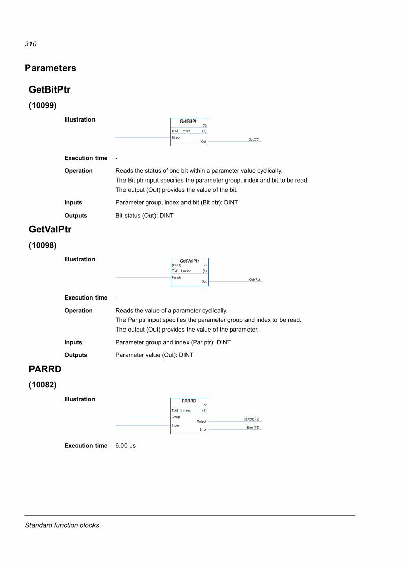
310
Parameters
GetBitPtr(10099)
Illustration
Execution time -
Operation Reads the status of one bit within a parameter value cyclically.The Bit ptr input specifies the parameter group, index and bit to be read.The output (Out) provides the value of the bit.
Inputs Parameter group, index and bit (Bit ptr): DINT
Outputs Bit status (Out): DINT
GetValPtr(10098)
Illustration
Execution time -
Operation Reads the value of a parameter cyclically.The Par ptr input specifies the parameter group and index to be read.The output (Out) provides the value of the parameter.
Inputs Parameter group and index (Par ptr): DINT
Outputs Parameter value (Out): DINT
PARRD(10082)
Illustration
Execution time 6.00 µs
GetBitPtr70
TLA1 1 msec (1)
Bit ptrOut
Out(70)
GetValPtr(DINT) 71
TLA1 1 msec (1)
Par ptrOut
Out(71)
PARRD72
TLA1 1 msec (1)
Group
IndexOutput
Output(72)
ErrorError(72)
Standard function blocks

311
Operation Reads the scaled value of a parameter (specified by the Group and Index inputs). If the parameter is a pointer parameter, the Output pin provides the number of the source parameter instead of its value.Error codes are indicated by the error output (Error) as follows:
See also blocks PARRDINTR and PARRDPTR.
Inputs Parameter group input (Group): DINTParameter index input (Index): DINT
Outputs Output (Output): DINTError output (Error): DINT
PARRDINTR(10101)
Illustration
Execution time -
Operation Reads the internal (non-scaled) value of a parameter (specified by the Group and Index inputs). The value is provided by the Output pin.Error codes are indicated by the error output (Error) as follows:
Note: Using this block may cause incompatibility issues when upgrading the application to another firmware version.
Inputs Parameter group (Group): DINTParameter index (Index): DINT
Outputs Output (Output): Boolean, INT, DINT, REAL, REAL24Error output (Error): DINT
PARRDPTR(10100)
Illustration
Execution time -
Error code Description0 No error
<> 0 Error
PARRDINTR(BOOL) 73
TLA1 1 msec (1)
Group
IndexOutput
Output(73)
ErrorError(73)
Error code Description0 No error or busy
<> 0 Error
PARRDPTR(BOOL) 74
TLA1 1 msec (1)
Group
IndexOutput
Output(74)
ErrorError(74)
Standard function blocks
312
Operation Reads the internal (non-scaled) value of the source of a pointer parameter. The pointer parameter is specified using the Group and Index inputs.The value of the source selected by the pointer parameter is provided by the Output pin.Error codes are indicated by the error output (Error) as follows:
Inputs Parameter group (Group): DINTParameter index (Index): DINT
Outputs Output (Output): Boolean, INT, DINT, REAL, REAL24Error output (Error): DINT
PARWR(10080)
Illustration
Execution time 14.50 µs
Operation The input value (IN) is written to the defined parameter (Group and Index). The new parameter value is stored to the flash memory if the store input (Store) is 1. Note: Cyclic parameter value storing can damage the memory unit. Parameter values should be stored only when necessary.Error codes are indicated by the error output (Error) as follows:
Inputs Input (IN): DINTParameter group input (Group): DINTParameter index input (Index): DINTStore input (Store): Boolean
Outputs Error output (Error): DINT
Error code Description0 No error or busy
<> 0 Error
PARWR75
TLA1 1 msec (1)
IN
Group
Index
Store
ErrorError(75)
Error code Description0 No error
<> 0 Error
Standard function blocks
313
Program structure
BOP(10105)
Illustration
Execution time -
Operation The BOP (Bundle OutPut) block collects the outputs of several different sources. The sources are connected to the B_Output pins. The B_Output pin that changed last is relayed to the Output pin.The block is intended for use with conditional IF-ENDIF structures. See the example under the IF block.
Inputs Values from different conditional branches (B_Output1…B_OutputN): INT, DINT, Boolean, REAL, REAL24
Outputs Output from currently active branch of a IF-ELSEIF structure or latest updated input value (Output): INT, DINT, Boolean, REAL, REAL24
ELSEIllustration
Execution time -
Operation See description of IF block.
Inputs -
Outputs -
ELSEIFIllustration
Execution time -
Operation See description of IF block.
Inputs Input (COND): Boolean
Outputs -
BOP(BOOL) 46
TLA2 10 msec (1)
B_Output1
B_Output2Output
Output(46)
Standard function blocks
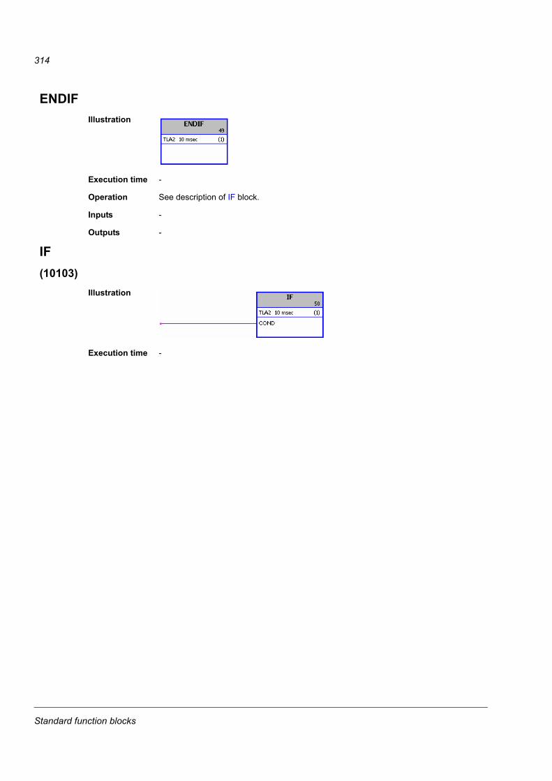
314
ENDIFIllustration
Execution time -
Operation See description of IF block.
Inputs -
Outputs -
IF(10103)
Illustration
Execution time -
Standard function blocks
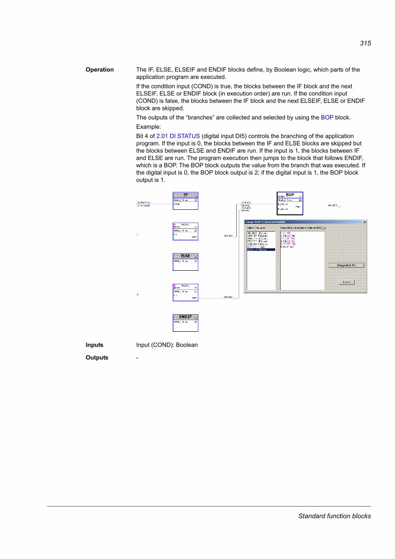
315
Operation The IF, ELSE, ELSEIF and ENDIF blocks define, by Boolean logic, which parts of the application program are executed.If the condition input (COND) is true, the blocks between the IF block and the next ELSEIF, ELSE or ENDIF block (in execution order) are run. If the condition input (COND) is false, the blocks between the IF block and the next ELSEIF, ELSE or ENDIF block are skipped.The outputs of the “branches” are collected and selected by using the BOP block.Example:Bit 4 of 2.01 DI STATUS (digital input DI5) controls the branching of the application program. If the input is 0, the blocks between the IF and ELSE blocks are skipped but the blocks between ELSE and ENDIF are run. If the input is 1, the blocks between IF and ELSE are run. The program execution then jumps to the block that follows ENDIF, which is a BOP. The BOP block outputs the value from the branch that was executed. If the digital input is 0, the BOP block output is 2; if the digital input is 1, the BOP block output is 1.
Inputs Input (COND): Boolean
Outputs -
Standard function blocks
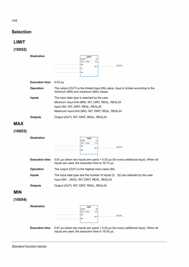
316
Selection
LIMIT(10052)
Illustration
Execution time 0.53 µs
Operation The output (OUT) is the limited input (IN) value. Input is limited according to the minimum (MN) and maximum (MX) values.
Inputs The input data type is selected by the user.Minimum input limit (MN): INT, DINT, REAL, REAL24Input (IN): INT, DINT, REAL, REAL24Maximum input limit (MX): INT, DINT, REAL, REAL24
Outputs Output (OUT): INT, DINT, REAL, REAL24
MAX(10053)
Illustration
Execution time 0.81 µs (when two inputs are used) + 0.53 µs (for every additional input). When all inputs are used, the execution time is 16.73 µs.
Operation The output (OUT) is the highest input value (IN).
Inputs The input data type and the number of inputs (2…32) are selected by the user.Input (IN1…IN32): INT, DINT, REAL, REAL24
Outputs Output (OUT): INT, DINT, REAL, REAL24
MIN(10054)
Illustration
Execution time 0.81 µs (when two inputs are used) + 0.52 µs (for every additional input). When all inputs are used, the execution time is 16.50 µs.
LIMIT(DINT) 76
TLA1 1 msec (1)
MN
IN
MX
OUTOUT(76)
MAX(DINT) 77
TLA1 1 msec (1)
IN1
IN2OUT
OUT(77)
MIN(DINT) 78
TLA1 1 msec (1)
IN1
IN2OUT
OUT(78)
Standard function blocks
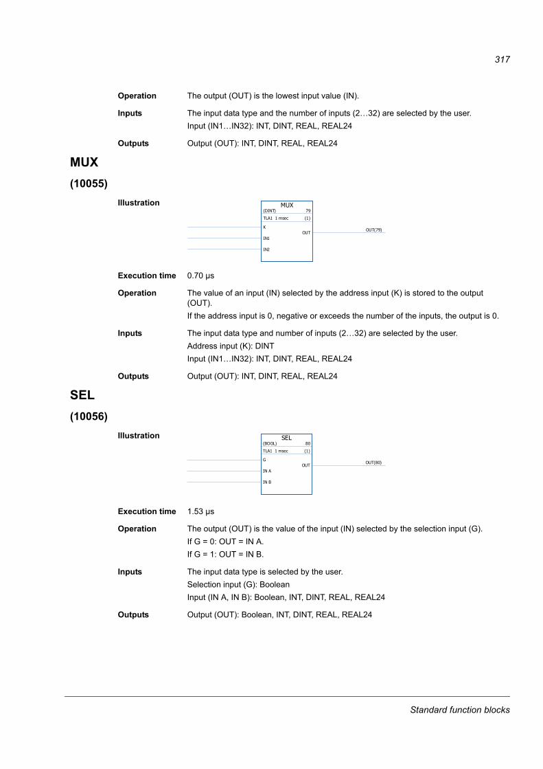
317
Operation The output (OUT) is the lowest input value (IN).
Inputs The input data type and the number of inputs (2…32) are selected by the user.Input (IN1…IN32): INT, DINT, REAL, REAL24
Outputs Output (OUT): INT, DINT, REAL, REAL24
MUX(10055)
Illustration
Execution time 0.70 µs
Operation The value of an input (IN) selected by the address input (K) is stored to the output (OUT).If the address input is 0, negative or exceeds the number of the inputs, the output is 0.
Inputs The input data type and number of inputs (2…32) are selected by the user.Address input (K): DINTInput (IN1…IN32): INT, DINT, REAL, REAL24
Outputs Output (OUT): INT, DINT, REAL, REAL24
SEL(10056)
Illustration
Execution time 1.53 µs
Operation The output (OUT) is the value of the input (IN) selected by the selection input (G).If G = 0: OUT = IN A.If G = 1: OUT = IN B.
Inputs The input data type is selected by the user.Selection input (G): BooleanInput (IN A, IN B): Boolean, INT, DINT, REAL, REAL24
Outputs Output (OUT): Boolean, INT, DINT, REAL, REAL24
MUX(DINT) 79
TLA1 1 msec (1)
K
IN1
IN2
OUTOUT(79)
SEL(BOOL) 80
TLA1 1 msec (1)
G
IN A
IN B
OUTOUT(80)
Standard function blocks

318
Switch & Demux
DEMUX-I(10061)
Illustration
Execution time 1.38 µs (when two outputs are used) + 0.30 µs (for every additional output). When all outputs are used, the execution time is 10.38 µs.
Operation Input (I) value is stored to the output (OA1…OA32) selected by the address input (A). All other outputs are 0.If the address input is 0, negative or exceeds the number of the outputs, all outputs are 0.
Inputs The input data type is selected by the user.Address input (A): DINTInput (I): INT, DINT, Boolean, REAL, REAL24
Outputs The number of the output channels (1…32) is selected by the user.Output (OA1…OA32): INT, DINT, REAL, REAL24, Boolean
DEMUX-MI(10062)
Illustration
Execution time 0.99 µs (when two outputs are used) + 0.25 µs (for every additional output). When all outputs are used, the execution time is 8.4 µs.
DEMUX-I(BOOL) 81
TLA1 1 msec (1)
A
IOA1
OA1(81)
OA2OA2(81)
DEMUX-MI(BOOL) 82
TLA1 1 msec (1)
A
R
L
S
I
OA1OA1(82)
OA2OA2(82)
Standard function blocks
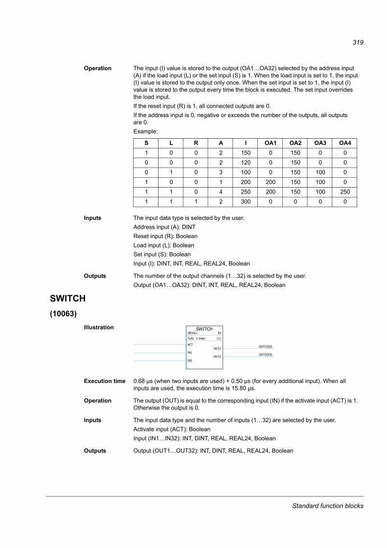
319
Operation The input (I) value is stored to the output (OA1…OA32) selected by the address input (A) if the load input (L) or the set input (S) is 1. When the load input is set to 1, the input (I) value is stored to the output only once. When the set input is set to 1, the input (I) value is stored to the output every time the block is executed. The set input overrides the load input.If the reset input (R) is 1, all connected outputs are 0.If the address input is 0, negative or exceeds the number of the outputs, all outputs are 0.Example:
Inputs The input data type is selected by the user.Address input (A): DINTReset input (R): BooleanLoad input (L): BooleanSet input (S): BooleanInput (I): DINT, INT, REAL, REAL24, Boolean
Outputs The number of the output channels (1…32) is selected by the user.Output (OA1…OA32): DINT, INT, REAL, REAL24, Boolean
SWITCH(10063)
Illustration
Execution time 0.68 µs (when two inputs are used) + 0.50 µs (for every additional input). When all inputs are used, the execution time is 15.80 µs.
Operation The output (OUT) is equal to the corresponding input (IN) if the activate input (ACT) is 1. Otherwise the output is 0.
Inputs The input data type and the number of inputs (1…32) are selected by the user.Activate input (ACT): BooleanInput (IN1…IN32): INT, DINT, REAL, REAL24, Boolean
Outputs Output (OUT1…OUT32): INT, DINT, REAL, REAL24, Boolean
S L R A I OA1 OA2 OA3 OA41 0 0 2 150 0 150 0 0
0 0 0 2 120 0 150 0 0
0 1 0 3 100 0 150 100 0
1 0 0 1 200 200 150 100 0
1 1 0 4 250 200 150 100 250
1 1 1 2 300 0 0 0 0
SWITCH(BOOL) 83
TLA1 1 msec (1)
ACT
IN1
IN2
OUT1OUT1(83)
OUT2OUT2(83)
Standard function blocks
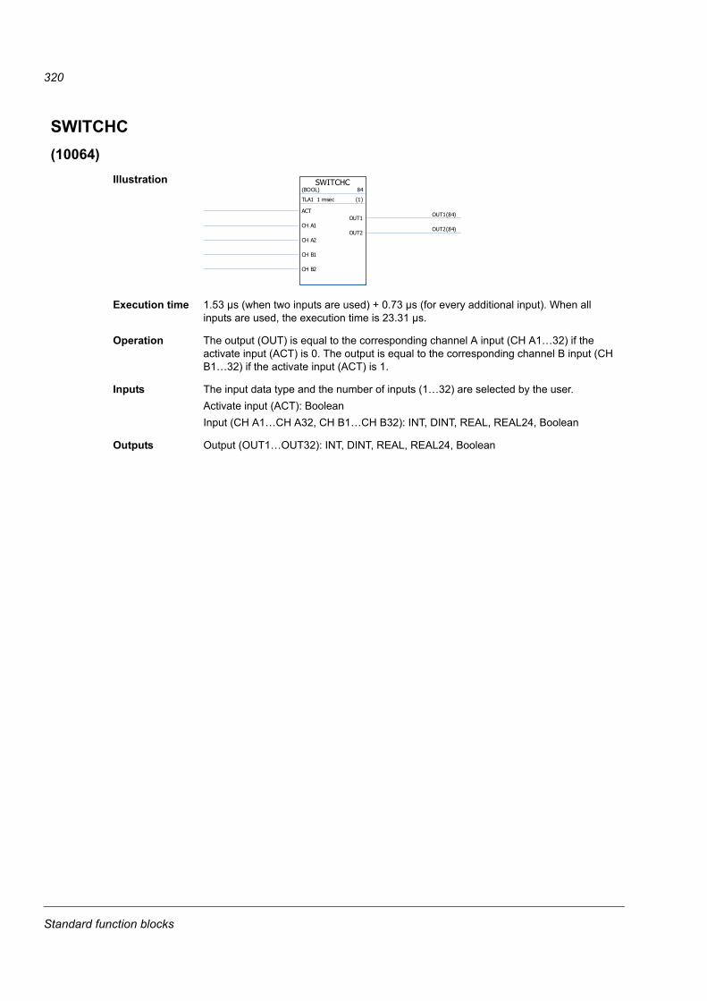
320
SWITCHC(10064)
Illustration
Execution time 1.53 µs (when two inputs are used) + 0.73 µs (for every additional input). When all inputs are used, the execution time is 23.31 µs.
Operation The output (OUT) is equal to the corresponding channel A input (CH A1…32) if the activate input (ACT) is 0. The output is equal to the corresponding channel B input (CH B1…32) if the activate input (ACT) is 1.
Inputs The input data type and the number of inputs (1…32) are selected by the user.Activate input (ACT): BooleanInput (CH A1…CH A32, CH B1…CH B32): INT, DINT, REAL, REAL24, Boolean
Outputs Output (OUT1…OUT32): INT, DINT, REAL, REAL24, Boolean
SWITCHC(BOOL) 84
TLA1 1 msec (1)
ACT
CH A1
CH A2
CH B1
CH B2
OUT1OUT1(84)
OUT2OUT2(84)
Standard function blocks
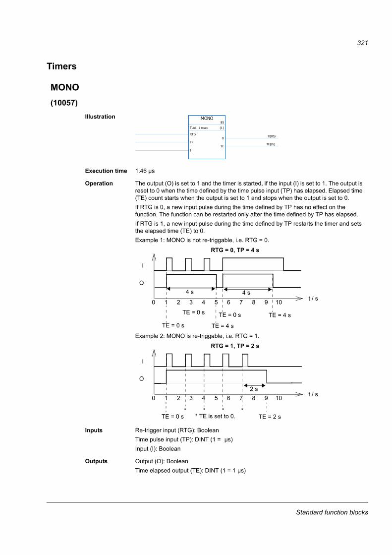
321
Timers
MONO(10057)
Illustration
Execution time 1.46 µs
Operation The output (O) is set to 1 and the timer is started, if the input (I) is set to 1. The output is reset to 0 when the time defined by the time pulse input (TP) has elapsed. Elapsed time (TE) count starts when the output is set to 1 and stops when the output is set to 0.If RTG is 0, a new input pulse during the time defined by TP has no effect on the function. The function can be restarted only after the time defined by TP has elapsed.If RTG is 1, a new input pulse during the time defined by TP restarts the timer and sets the elapsed time (TE) to 0.Example 1: MONO is not re-triggable, i.e. RTG = 0.
Example 2: MONO is re-triggable, i.e. RTG = 1.
Inputs Re-trigger input (RTG): BooleanTime pulse input (TP): DINT (1 = µs)Input (I): Boolean
Outputs Output (O): BooleanTime elapsed output (TE): DINT (1 = 1 µs)
MONO85
TLA1 1 msec (1)
RTG
TP
I
OO(85)
TETE(85)
I
O
RTG = 0, TP = 4 s
0 1 t / s2 3 4 5 6 7 8 9 104 s4 s
TE = 0 s TE = 4 s
TE = 0 s TE = 4 sTE = 0 s
I
O
RTG = 1, TP = 2 s
0 1 t / s2 3 4 5 6 7 8 9 102 s
TE = 0 s TE = 2 s* TE is set to 0.* * * *
Standard function blocks

322
TOF(10058)
Illustration
Execution time 1.10 µs
Operation The output (Q) is set to 1, when the input (IN) is set to 1. The output is reset to zero when the input has been 0 for a time defined by the pulse time input (PT).Elapsed time count (ET) starts when the input is set to 0 and stops when the input is set to 1.Example:
Inputs Input (IN): BooleanPulse time input (PT): DINT (1 = 1 µs)
Outputs Elapsed time output (ET): DINT (1 = 1 µs)Output (Q): Boolean
TON(10059)
Illustration
Execution time 1.22 µs
TOF86
TLA1 1 msec (1)
IN
PTET
ET(86)
QQ(86)
IN
Q
PT
ET ET ET
PT
TON87
TLA1 1 msec (1)
IN
PTET
ET(87)
QQ(87)
Standard function blocks
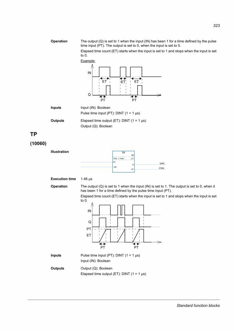
323
Operation The output (Q) is set to 1 when the input (IN) has been 1 for a time defined by the pulse time input (PT). The output is set to 0, when the input is set to 0.Elapsed time count (ET) starts when the input is set to 1 and stops when the input is set to 0.Example:
Inputs Input (IN): BooleanPulse time input (PT): DINT (1 = 1 µs)
Outputs Elapsed time output (ET): DINT (1 = 1 µs)Output (Q): Boolean
TP(10060)
Illustration
Execution time 1.46 µs
Operation The output (Q) is set to 1 when the input (IN) is set to 1. The output is set to 0, when it has been 1 for a time defined by the pulse time input (PT).Elapsed time count (ET) starts when the input is set to 1 and stops when the input is set to 0.
Inputs Pulse time input (PT): DINT (1 = 1 µs)Input (IN): Boolean
Outputs Output (Q): BooleanElapsed time output (ET): DINT (1 = 1 µs)
IN
QPTPT
ET ET ET
TP88
TLA1 1 msec (1)
PT
>INQ
Q(88)
ETET(88)
IN
Q
ET
PT
PTPT
Standard function blocks

324
Standard function blocks

325
Application program template
What this chapter containsThis chapter presents the application program template as displayed by the DriveSPC tool after empty template upload (Drive - Upload Template from Drive).
Application program template

326
PO
S F
EED
BA
CK
36
POSC
TR 5
00 μ
sec
(1)
1.12
PO
S A
CT
1.13
PO
S 2N
D E
NC
AC
TUA
L V
ALU
ES8
MIS
C_6
2 m
sec
(1)
1.02
-10
0000
1.03
FR
EQUE
NCY
1.04
CUR
RENT
1.05
CU
RREN
T PE
RC
1.06
TO
RQU
E
1.07
DC
-VO
LTA
GE
1.14
SPE
ED E
STIM
ATED
1.15
TEM
P IN
VER
TER
1.16
TEM
P B
C
1.20
BRA
KE R
ES L
OAD
1.22
INV
ERTE
R PO
WER
1.26
ON
TIM
E CO
UNTE
R
1.27
RU
N TI
ME
CO
UNTE
R
1.28
FAN
ON-
TIM
E
1.31
MEC
H T
IME
CON
ST
1.38
TEM
P IN
T BO
ARD
Page
1
Sign
als
FWA
com
patib
ility
lev
el =
1.5
1Fi
rmw
are
Libr
ary
ID =
1, v
er =
1.0
Stan
dard
Lib
rary
ID
= 1
0000
, ver
= 1
.1
Base
d on
Cust
omer
Cust
. Doc
. No.
Dat
e
Prep
ared
App
rove
dPr
ojec
t nam
e
Title
Doc
. des
.
Resp
. dep
t.D
oc. N
o.
Application program template
327
DI
16
IOCT
RL
2 m
sec
(1)
12.1
3 D
I IN
VER
T M
ASK
(Driv
e va
lue)
2.01
DI
STAT
US
RO
17
IOCT
RL
2 m
sec
(2)
< 1
2.12
RO
1 O
UT
PTR
(Driv
e va
lue)
2.02
RO
STA
TUS
DIO
118
IOCT
RL
2 m
sec
(3)
12
.01
DIO
1 C
ONF
(Driv
e va
lue)
< 1
2.04
DIO
1 O
UT
PTR
(Driv
e va
lue)
2.03
DIO
STA
TUS
2.03
Bit 0
DIO
219
IOCT
RL
2 m
sec
(4)
12
.02
DIO
2 C
ONF
(Driv
e va
lue)
< 1
2.05
DIO
2 O
UT
PTR
(Driv
e va
lue)
12
.14
DIO
2 F
MAX
(Driv
e va
lue)
12
.15
DIO
2 F
MIN
(Driv
e va
lue)
12
.16
DIO
2 F
MAX
SCA
LE(D
rive
valu
e)
12
.17
DIO
2 F
MIN
SC
ALE
(Driv
e va
lue)
2.03
DIO
STA
TUS
2.03
Bit 1
2.10
DIO
2 FR
EQ I
N
DIO
320
IOCT
RL
2 m
sec
(5)
12
.03
DIO
3 C
ONF
(Driv
e va
lue)
< 1
2.06
DIO
3 O
UT
PTR
(Driv
e va
lue)
< 1
2.07
DIO
3 F
OUT
PTR
[ SP
EED
ACT
](7
/ 1
.01)
12
.08
DIO
3 F
MAX
(Driv
e va
lue)
12
.09
DIO
3 F
MIN
(Driv
e va
lue)
12
.10
DIO
3 F
MAX
SCA
LE(D
rive
valu
e)
12
.11
DIO
3 F
MIN
SC
ALE
(Driv
e va
lue)
2.03
DIO
STA
TUS
2.03
Bit 2
2.11
DIO
3 FR
EQ O
UT
Page
2
Dig
ital I/
OFW
A co
mpa
tibili
ty lev
el =
1.5
1Fi
rmw
are
Libr
ary
ID =
1, ve
r =
1.0
Stan
dard
Lib
rary
ID
= 1
0000
, ver
= 1
.1
Base
d on
Cust
omer
Cust
. D
oc. N
o.D
ate
Prep
ared
App
rove
dPr
ojec
t nam
e
Title
Doc
. des
.
Resp
. dep
t.D
oc. N
o.
Application program template
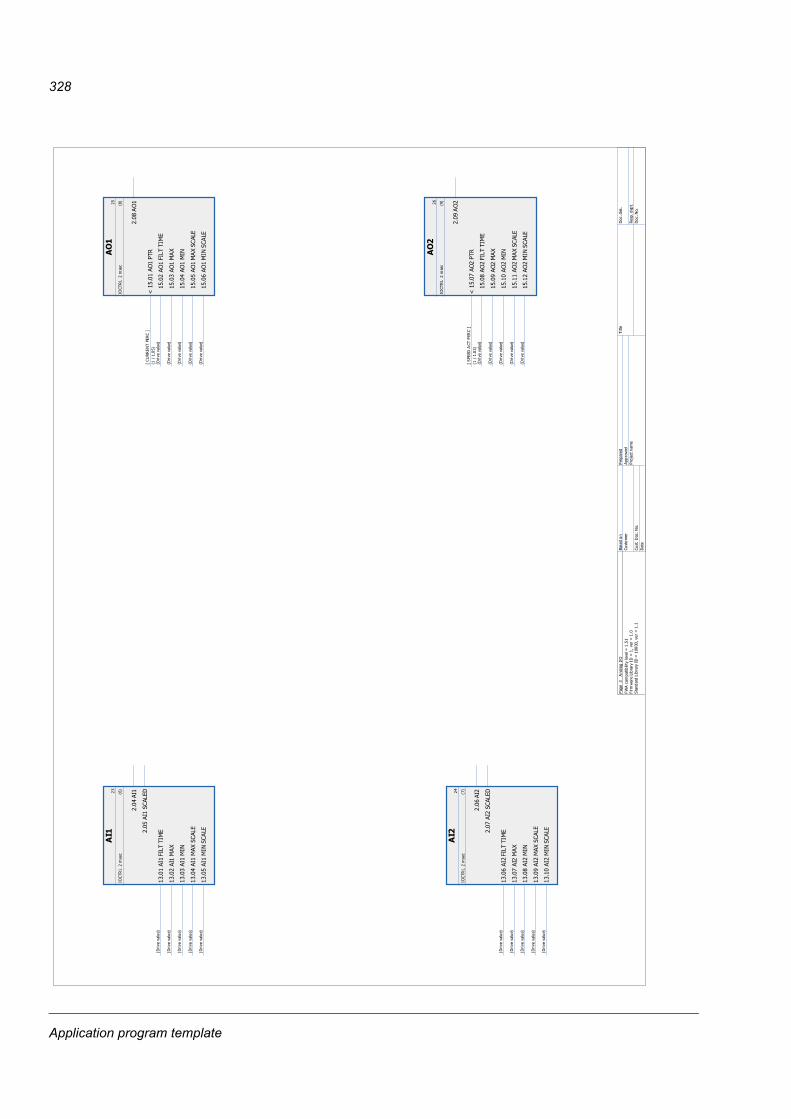
328
AI123
IOCT
RL
2 m
sec
(6)
13.0
1 AI
1 FI
LT T
IME
(Driv
e va
lue)
13.0
2 AI
1 M
AX
(Driv
e va
lue)
13.0
3 AI
1 M
IN(D
rive
valu
e)
13.0
4 AI
1 M
AX S
CALE
(Driv
e va
lue)
13.0
5 AI
1 M
IN S
CALE
(Driv
e va
lue)
2.04
AI1
2.05
AI1
SCA
LED
AI2
24
IOCT
RL
2 m
sec
(7)
13.0
6 AI
2 FI
LT T
IME
(Driv
e va
lue)
13.0
7 AI
2 M
AX
(Driv
e va
lue)
13.0
8 AI
2 M
IN(D
rive
valu
e)
13.0
9 AI
2 M
AX S
CALE
(Driv
e va
lue)
13.1
0 AI
2 M
IN S
CALE
(Driv
e va
lue)
2.06
AI2
2.07
AI2
SCA
LED
AO
125
IOCT
RL
2 m
sec
(8)
< 1
5.01
AO
1 PT
R[
CURR
ENT
PERC
](1
/ 1
.05)
15
.02
AO1
FILT
TIM
E(D
rive
valu
e)
15
.03
AO1
MA
X(D
rive
valu
e)
15
.04
AO1
MIN
(Driv
e va
lue)
15
.05
AO1
MA
X SC
ALE
(Driv
e va
lue)
15
.06
AO1
MIN
SCA
LE(D
rive
valu
e)
2.08
AO
1
AO
226
IOCT
RL
2 m
sec
(9)
< 1
5.07
AO
2 PT
R[
SPEE
D A
CT P
ERC
](1
/ 1
.02)
15
.08
AO2
FILT
TIM
E(D
rive
valu
e)
15
.09
AO2
MA
X(D
rive
valu
e)
15
.10
AO2
MIN
(Driv
e va
lue)
15
.11
AO2
MA
X SC
ALE
(Driv
e va
lue)
15
.12
AO2
MIN
SCA
LE(D
rive
valu
e)
2.09
AO
2
Page
3
Ana
log
I/O
FWA
com
patib
ility
lev
el =
1.5
1Fi
rmw
are
Libr
ary
ID =
1, ve
r =
1.0
Stan
dard
Lib
rary
ID
= 1
0000
, ver
= 1
.1
Base
d on
Cust
omer
Cust
. D
oc. N
o.D
ate
Prep
ared
App
rove
dPr
ojec
t nam
e
Title
Doc
. des
.
Resp
. dep
t.D
oc. N
o.
Application program template

329
FIEL
DB
US
36
MIS
C_2
500
μse
c(1
)
50
.01
FBA
ENAB
LE(D
rive
val
ue)
50
.02
COM
M L
OSS
FU
NC
(Dri
ve v
alue
)
50
.03
COM
M L
OSS
T O
UT
(Dri
ve v
alue
)
50
.04
FBA
REF1
MO
DES
EL(D
rive
val
ue)
50
.05
FBA
REF2
MO
DES
EL(D
rive
val
ue)
< 5
0.06
FBA
ACT
1 TR
SRC
[ SP
EED
ACT
](7
/ 1
.01)
< 5
0.07
FBA
ACT
2 TR
SRC
[ T
ORQ
UE
](1
/ 1
.06)
< 5
0.08
FBA
SW
B12
SR
C(D
rive
val
ue)
< 5
0.09
FBA
SW
B13
SR
C(D
rive
val
ue)
< 5
0.10
FBA
SW
B14
SR
C(D
rive
val
ue)
< 5
0.11
FBA
SW
B15
SR
C(D
rive
val
ue)
50
.12
FBA
CYCL
E TI
ME
(Dri
ve v
alue
)
50
.20
FB M
AIN
SW
FU
NC
(Dri
ve v
alue
)
2.12
FBA
MAI
N C
W
2.13
FBA
MAI
N S
W
2.14
FBA
MAI
N R
EF1
2.15
FBA
MAI
N R
EF2
D2D
CO
MM
UN
ICA
TIO
N 44
MIS
C_2
500
μse
c(2
)
57
.01
LIN
K M
OD
E(D
rive
valu
e)
57
.02
COM
M L
OSS
FU
NC
(Driv
e va
lue)
57
.03
NO
DE
ADD
RESS
(Driv
e va
lue)
57
.04
FOLL
OW
ER M
ASK
1(D
rive
valu
e)
57
.05
FOLL
OW
ER M
ASK
2(D
rive
valu
e)
< 5
7.06
REF
1 S
RC
[ SPE
EDRE
F RA
MPE
D ]
(6 /
3.0
4)
< 5
7.07
REF
2 S
RC
[ T
OR
Q R
EF T
O T
C ]
(8 /
3.1
3)
< 5
7.08
FO
LLO
WER
CW
SRC
[ D2D
FO
LLO
WER
CW
](4
/ 2
.18)
57
.09
KERN
EL S
YNC
MO
DE
(Driv
e va
lue)
57
.10
KERN
EL S
YNC
OFF
S(D
rive
valu
e)
57
.11
REF
1 M
SG T
YPE
(Driv
e va
lue)
57
.12
REF1
MC
GRO
UP(D
rive
valu
e)
57
.13
NEX
T RE
F1 M
C G
RP(D
rive
valu
e)
57
.14
NR
REF
1 M
C G
RPS
(Driv
e va
lue)
2.17
D2D
MAI
N CW
2.19
D2D
REF
1
2.20
D2D
REF
2
MEC
H B
RA
KE
CTR
L30
MIS
C_3
2 m
sec
(2)
35
.01
BRAK
E C
ONT
ROL
(Dri
ve v
alue
)
< 3
5.02
BRA
KE A
CKN
OW
L(D
rive
val
ue)
35
.03
BRAK
E O
PEN
DEL
AY(D
rive
val
ue)
35
.04
BRAK
E C
LOSE
DLY
(Dri
ve v
alue
)
35
.05
BRAK
E C
LOSE
SPD
(Dri
ve v
alue
)
35
.06
BRAK
E O
PEN
TO
RQ(D
rive
val
ue)
< 3
5.07
BRA
KE C
LOSE
REQ
(Dri
ve v
alue
)
< 3
5.08
BRA
KE O
PEN
HO
LD(D
rive
val
ue)
35
.09
BRAK
E FA
ULT
FU
NC
(Dri
ve v
alue
)
3.14
BRA
KE T
ORQ
MEM
3.15
BRA
KE C
OM
MA
ND
DR
IVE
LOG
IC21
MIS
C_3
2 m
sec
(3)
10
.01
EXT1
STA
RT F
UN
C(D
rive
val
ue)
< 1
0.02
EXT
1 ST
ART
IN1
(Dri
ve v
alue
)
< 1
0.03
EXT
1 ST
ART
IN2
(Dri
ve v
alue
)
10
.04
EXT2
STA
RT F
UN
C(D
rive
val
ue)
< 1
0.05
EXT
2 ST
ART
IN1
(Dri
ve v
alue
)
< 1
0.06
EXT
2 ST
ART
IN2
(Dri
ve v
alue
)
< 1
0.07
JO
G1 S
TART
(Dri
ve v
alue
)
< 1
0.08
FAU
LT R
ESET
SEL
(Dri
ve v
alue
)
< 1
0.09
RU
N E
NABL
E(D
rive
val
ue)
< 1
0.10
EM
STO
P O
FF3
(Dri
ve v
alue
)
< 1
0.11
EM
STO
P O
FF1
(Dri
ve v
alue
)
10
.12
STAR
T IN
HIB
IT(D
rive
val
ue)
< 1
0.13
FB
CW
USE
D[ F
BA M
AIN
CW
](4
/ 2
.12)
< 1
0.14
JO
G2 S
TART
(Dri
ve v
alue
)
< 1
0.15
JO
G E
NABL
E(D
rive
val
ue)
< 1
0.16
D2D
CW
USE
D[ D
2D M
AIN
CW
](4
/ 2
.17)
< 1
0.17
STA
RT E
NABL
E(D
rive
val
ue)
2.18
D2D
FO
LLO
WER
CW
6.01
STA
TUS
WO
RD
1
6.02
STA
TUS
WO
RD
2
6.03
SPE
ED C
TRL
STAT
6.05
LIM
IT W
ORD
1
6.07
TO
RQ L
IM S
TATU
S
6.09
PO
S CT
RL
STAT
US
6.10
PO
S CT
RL
STAT
US2
6.11
PO
S CO
RR
STAT
US
STA
RT/
STO
P M
OD
E22
MIS
C_3
2 m
sec
(4)
11.0
1 ST
ART
MO
DE
(Dri
ve v
alue
)
11.0
2 D
C M
AGN
TIM
E(D
rive
val
ue)
11.0
3 ST
OP
MO
DE
(Dri
ve v
alue
)
11.0
4 D
C H
OLD
SPE
ED(D
rive
val
ue)
11.0
5 D
C H
OLD
CU
R RE
F(D
rive
val
ue)
11.0
6 D
C H
OLD
(Dri
ve v
alue
)
11.0
7 AU
TOPH
ASIN
G M
OD
E(D
rive
val
ue)
Page
4
Driv
e Lo
gic
FWA
com
patib
ility
leve
l = 1
.51
Firm
war
e Li
brar
y ID
= 1
, ve
r =
1.0
Stan
dard
Lib
rary
ID
= 1
0000
, ve
r =
1.1
Base
d on
Cus
tom
er
Cus
t. D
oc.
No.
Dat
e
Prep
ared
App
rove
dPr
ojec
t nam
e
Title
Doc
. des
.
Res
p. d
ept.
Doc
. No.
Application program template
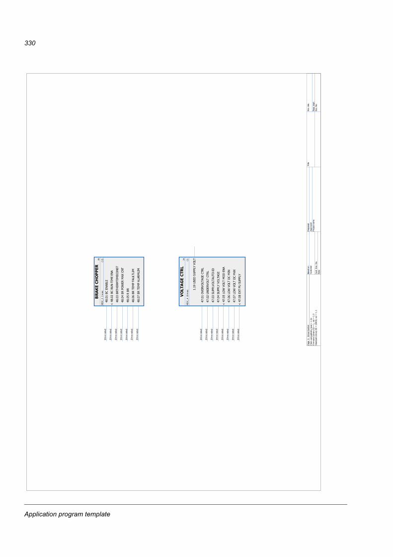
330
BR
AK
E C
HO
PP
ER35
MIS
C_3
2 m
sec
(11)
48
.01
BC E
NAB
LE(D
rive
valu
e)
< 4
8.02
BC
RUN
-TIM
E EN
A(D
rive
valu
e)
48
.03
BRTH
ERM
TIM
ECO
NST
(Driv
e va
lue)
48
.04
BR P
OW
ER M
AX C
NT
(Driv
e va
lue)
48
.05
R B
R(D
rive
valu
e)
48
.06
BR T
EMP
FAU
LTLI
M(D
rive
valu
e)
48
.07
BR T
EMP
ALA
RM
LIM
(Driv
e va
lue)
VO
LTA
GE
CTR
L34
MIS
C_4
10
mse
c(1
)
47
.01
OVE
RVO
LTAG
E CT
RL(D
rive
valu
e)
47
.02
UND
ERV
OLT
CTR
L(D
rive
valu
e)
47
.03
SUPP
LVO
LTAU
TO-I
D(D
rive
valu
e)
47
.04
SUPP
LY V
OLT
AGE
(Driv
e va
lue)
< 4
7.05
LO
W V
OLT
MO
D E
NA
(Driv
e va
lue)
47
.06
LOW
VO
LT D
C M
IN(D
rive
valu
e)
47
.07
LOW
VO
LT D
C M
AX(D
rive
valu
e)
< 4
7.08
EXT
PU
SUP
PLY
(Driv
e va
lue)
1.19
USE
D S
UPPL
Y V
OLT
Page
5
Driv
e Co
ntro
lFW
A co
mpa
tibili
ty lev
el =
1.5
1Fi
rmw
are
Libr
ary
ID =
1, ve
r =
1.0
Stan
dard
Lib
rary
ID
= 1
0000
, ver
= 1
.1
Base
d on
Cust
omer
Cust
. D
oc. N
o.D
ate
Prep
ared
App
rove
dPr
ojec
t nam
e
Title
Doc
. des
.
Resp
. dep
t.D
oc. N
o.
Application program template
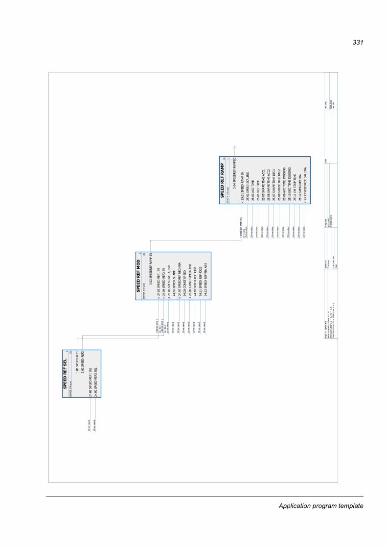
331
SPE
ED R
EF S
EL
3
SPD
REF
500
μse
c(1
)
24.0
1 SP
EED
REF
1 SE
L(D
rive
valu
e)
24.0
2 SP
EED
REF
2 SE
L(D
rive
valu
e)
3.01
SPE
ED R
EF1
3.02
SPE
ED R
EF2
SPE
ED R
EF M
OD
4
SPD
REF
500
μse
c(2
)
< 2
4.03
SPE
ED R
EF1
IN[
SPEE
D R
EF1
](6
/ 3
.01)
< 2
4.04
SPE
ED R
EF2
IN[
SPEE
D R
EF2
](6
/ 3
.02)
< 2
4.05
SPE
ED R
EF 1
/2SE
L(D
rive
valu
e)
2
4.06
SPE
ED S
HAR
E(D
rive
valu
e)
< 2
4.07
SPE
EDRE
F N
EG E
NA
(Driv
e va
lue)
2
4.08
CO
NST
SP
EED
(Driv
e va
lue)
< 2
4.09
CO
NST
SPEE
D E
NA(D
rive
valu
e)
2
4.10
SPE
ED R
EF J
OG
1(D
rive
valu
e)
2
4.11
SPE
ED R
EF J
OG
2(D
rive
valu
e)
2
4.12
SPE
ED R
EFM
IN A
BS
(Driv
e va
lue)
3.03
SPE
EDR
EF R
AMP
IN
SPE
ED R
EF R
AM
P28
SPD
CTR
25
0 μs
ec(1
)
< 2
5.01
SPE
ED R
AM
P IN
[ SP
EED
REF
RAM
P IN
](6
/ 3
.03)
25
.02
SPEE
D S
CALI
NG
(Driv
e va
lue)
25
.03
ACC
TIM
E(D
rive
valu
e)
25
.04
DEC
TIM
E(D
rive
valu
e)
25
.05
SHA
PE T
IME
ACC1
(Driv
e va
lue)
25
.06
SHA
PE T
IME
ACC2
(Driv
e va
lue)
25
.07
SHA
PE T
IME
DEC
1(D
rive
valu
e)
25
.08
SHA
PE T
IME
DEC
2(D
rive
valu
e)
25
.09
ACC
TIM
E JO
GGIN
G(D
rive
valu
e)
25
.10
DEC
TIM
E JO
GGI
NG(D
rive
valu
e)
25
.11
EM S
TOP
TIM
E(D
rive
valu
e)
25
.12
SPEE
DRE
F BA
L(D
rive
valu
e)
< 2
5.13
SPE
EDR
EF B
AL E
NA
(Driv
e va
lue)
3.04
SPE
EDRE
F RA
MPE
D
Page
6
Sp
eed
Ref
FWA
com
patib
ility
leve
l = 1
.51
Firm
war
e Li
brar
y ID
= 1
, ve
r =
1.0
Stan
dard
Lib
rary
ID =
100
00,
ver
= 1
.1
Base
d on
Cust
omer
Cust
. Doc
. No.
Dat
e
Prep
ared
App
rove
dPr
ojec
t na
me
Title
Doc
. de
s.
Resp
. dep
t.D
oc. N
o.
Application program template
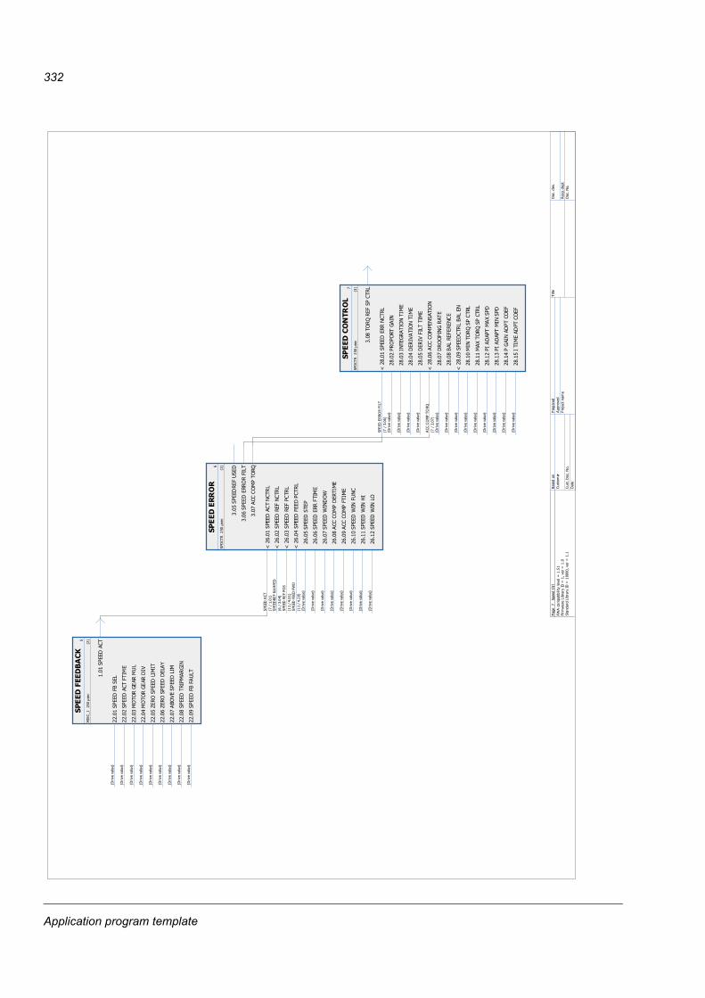
332
SPE
ED E
RR
OR
6
SPD
CTR
250
μse
c(2
)
< 2
6.01
SPE
ED A
CT
NCT
RL
SPE
ED A
CT(7
/ 1
.01)
< 2
6.02
SPE
ED R
EF N
CTR
LSP
EED
REF
RAM
PED
(6 /
3.0
4)
< 2
6.03
SPE
ED R
EF P
CTR
LSPE
ED R
EF P
OS
(11
/ 4.0
1)
< 2
6.04
SPE
ED F
EED
PCT
RL
SPE
ED F
EED
FW
D(1
1 / 4
.20)
2
6.05
SPE
ED S
TEP
(Driv
e va
lue)
2
6.06
SPE
ED E
RR F
TIM
E(D
rive
valu
e)
2
6.07
SPE
ED W
IND
OW
(Driv
e va
lue)
2
6.08
ACC
CO
MP
DER
TIM
E(D
rive
valu
e)
2
6.09
ACC
CO
MP
FTIM
E(D
rive
valu
e)
2
6.10
SPE
ED W
IN F
UN
C(D
rive
valu
e)
2
6.11
SPE
ED W
IN H
I(D
rive
valu
e)
2
6.12
SPE
ED W
IN L
O(D
rive
valu
e)
3.05
SPE
EDRE
F U
SED
3.06
SPE
ED E
RRO
R FI
LT
3.07
ACC
CO
MP
TORQ
SPE
ED C
ON
TRO
L7
SPD
CTR
25
0 μs
ec(3
)
< 2
8.01
SPE
ED E
RR N
CTRL
SPEE
D E
RRO
R FI
LT(7
/ 3
.06)
28
.02
PRO
PORT
GA
IN(D
rive
valu
e)
28
.03
INTE
GRA
TIO
N T
IME
(Driv
e va
lue)
28
.04
DER
IVA
TIO
N T
IME
(Driv
e va
lue)
28
.05
DER
IV F
ILT
TIM
E(D
rive
valu
e)
< 2
8.06
ACC
CO
MPE
NSA
TIO
NA
CC C
OM
P TO
RQ(7
/ 3
.07)
28
.07
DR
OOP
ING
RAT
E(D
rive
valu
e)
28
.08
BAL
REF
EREN
CE
(Driv
e va
lue)
< 2
8.09
SPE
EDC
TRL
BAL
EN(D
rive
valu
e)
28
.10
MIN
TO
RQ S
P C
TRL
(Driv
e va
lue)
28
.11
MAX
TO
RQ S
P CT
RL
(Driv
e va
lue)
28
.12
PI A
DAP
T M
AX
SPD
(Driv
e va
lue)
28
.13
PI A
DAP
T M
IN S
PD(D
rive
valu
e)
28
.14
P G
AIN
AD
PT C
OEF
(Driv
e va
lue)
28
.15
I TI
ME
ADPT
CO
EF(D
rive
valu
e)
3.08
TO
RQ R
EF S
P CT
RL
SPE
ED F
EED
BA
CK
5
MIS
C_1
250
μse
c(2
)
22.0
1 SP
EED
FB
SEL
(Driv
e va
lue)
22.0
2 SP
EED
ACT
FTI
ME
(Driv
e va
lue)
22.0
3 M
OTO
R GE
AR M
UL
(Driv
e va
lue)
22.0
4 M
OTO
R GE
AR D
IV(D
rive
valu
e)
22.0
5 ZE
RO S
PEED
LIM
IT(D
rive
valu
e)
22.0
6 ZE
RO S
PEED
DEL
AY
(Driv
e va
lue)
22.0
7 A
BOVE
SP
EED
LIM
(Driv
e va
lue)
22.0
8 SP
EED
TRI
PMAR
GIN
(Driv
e va
lue)
22.0
9 SP
EED
FB
FA
ULT
(Driv
e va
lue)
1.01
SPE
ED A
CT
Page
7
Sp
eed
Ctrl
FWA
com
patib
ility
leve
l = 1
.51
Firm
war
e Li
brar
y ID
= 1
, ve
r =
1.0
Stan
dard
Lib
rary
ID =
100
00,
ver
= 1
.1
Base
d on
Cust
omer
Cust
. Doc
. No.
Dat
e
Prep
ared
App
rove
dPr
ojec
t na
me
Title
Doc
. de
s.
Resp
. dep
t.D
oc. N
o.
Application program template
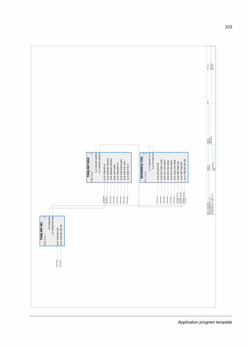
333
TOR
Q R
EF S
EL
1
TRQ
REF
500
μse
c(1
)
32.0
1 TO
RQ
REF
1 SE
L(D
rive
valu
e)
32.0
2 TO
RQ
REF
AD
D S
EL(D
rive
valu
e)
3.09
TO
RQ
REF
1
3.12
TO
RQ
UE R
EF A
DD
TOR
Q R
EF
MO
D2
TRQ
REF
500
μse
c(2
)
< 3
2.03
TO
RQ R
EF I
N[
TORQ
REF
1 ]
(8 /
3.0
9)
3
2.04
MA
XIM
UM T
ORQ
REF
(Driv
e va
lue)
3
2.05
MIN
IMUM
TO
RQ
REF
(Driv
e va
lue)
3
2.06
LO
AD S
HAR
E(D
rive
valu
e)
3
2.07
TO
RQ
RAM
P U
P(D
rive
valu
e)
3
2.08
TO
RQ
RAM
P D
OW
N(D
rive
valu
e)
3
2.09
RUS
H C
TRL
GAI
N(D
rive
valu
e)
3
2.10
RUS
H C
TRL
TI(D
rive
valu
e)
3.10
TO
RQ
REF
RAM
PED
3.11
TO
RQ
REF
RUS
HLI
M
RE
FER
ENC
E CT
RL
29
MIS
C_1
250
μse
c(3
)
< 3
4.01
EXT
1/EX
T2 S
EL(D
rive
valu
e)
< 3
4.02
EXT
1 M
OD
E 1/
2SEL
(Driv
e va
lue)
3
4.03
EXT
1 C
TRL
MO
DE1
(Driv
e va
lue)
3
4.04
EXT
1 C
TRL
MO
DE2
(Driv
e va
lue)
3
4.05
EXT
2 C
TRL
MO
DE1
(Driv
e va
lue)
3
4.07
LO
CAL
CTRL
MO
DE
(Driv
e va
lue)
< 3
4.08
TRE
F SP
EED
SR
CTO
RQ R
EF S
P CT
RL
(7 /
3.0
8)
< 3
4.09
TRE
F TO
RQ S
RCTO
RQ R
EF R
USH
LIM
(8 /
3.1
1)
< 3
4.10
TO
RQ R
EF A
DD
SRC
[ TO
RQU
E RE
F A
DD
](8
/ 3
.12)
3.13
TO
RQ R
EF T
O T
C
6.12
OP
MO
DE
ACK
Page
8
To
rque
Ref
FWA
com
patib
ility
leve
l = 1
.51
Firm
war
e Li
brar
y ID
= 1
, ve
r =
1.0
Stan
dard
Lib
rary
ID
= 1
0000
, ve
r =
1.1
Base
d on
Cust
omer
Cust
. Doc
. N
o.D
ate
Prep
ared
App
rove
dPr
ojec
t na
me
Title
Doc
. de
s.
Resp
. de
pt.
Doc
. N
o.
Application program template
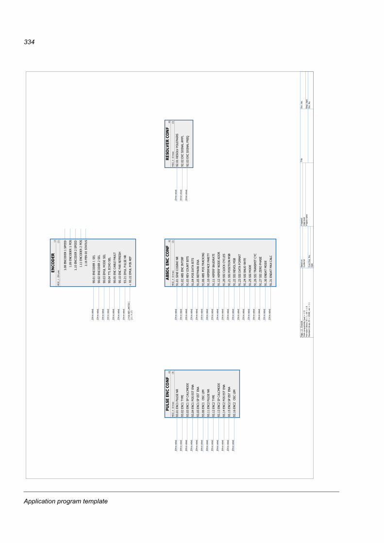
334
ENCO
DER
15
MIS
C_1
250
μse
c(1
)
90
.01
ENC
OD
ER 1
SEL
(Driv
e va
lue)
90
.02
ENC
OD
ER 2
SEL
(Driv
e va
lue)
90
.03
EMUL
MO
DE
SEL
(Driv
e va
lue)
90
.04
TTL
ECH
O S
EL(D
rive
valu
e)
90
.05
ENC
CA
BLE
FAU
LT(D
rive
valu
e)
90
.10
ENC
PA
R R
EFR
ESH
(Driv
e va
lue)
93
.21
EMUL
PUL
SE N
R(D
rive
valu
e)
< 9
3.22
EM
UL P
OS R
EF[
POS
REF
LIM
ITED
](1
1 / 4
.17)
1.08
EN
CO
DER
1 S
PEED
1.09
EN
CO
DER
1 P
OS
1.10
EN
CO
DER
2 S
PEED
1.11
EN
CO
DER
2 P
OS
2.16
FEN
DI
STAT
US
AB
SOL
ENC
CO
NF
42
MIS
C_4
10
mse
c(2
)
91.0
1 SI
NE
CO
SIN
E N
R(D
rive
valu
e)
91.0
2 AB
S EN
C IN
TERF
(Driv
e va
lue)
91.0
3 RE
V CO
UNT
BITS
(Driv
e va
lue)
91.0
4 PO
S D
ATA
BITS
(Driv
e va
lue)
91.0
5 RE
FMA
RK E
NA
(Driv
e va
lue)
91.0
6 AB
S PO
S TR
ACKI
NG(D
rive
valu
e)
91.1
0 H
IPER
FAC
E PA
RITY
(Driv
e va
lue)
91.1
1 H
IPER
F BA
UDR
ATE
(Driv
e va
lue)
91.1
2 H
IPER
F N
OD
E A
DD
R(D
rive
valu
e)
91.2
0 SS
I CL
OC
K CY
CLE
S(D
rive
valu
e)
91.2
1 SS
I PO
SITI
ON
MSB
(Driv
e va
lue)
91.2
2 SS
I RE
VOL
MSB
(Driv
e va
lue)
91.2
3 SS
I D
ATA
FO
RMA
T(D
rive
valu
e)
91.2
4 SS
I BA
UD
RA
TE(D
rive
valu
e)
91.2
5 SS
I M
OD
E(D
rive
valu
e)
91.2
6 SS
I TR
ANSM
IT C
YC(D
rive
valu
e)
91.2
7 SS
I ZE
RO P
HAS
E(D
rive
valu
e)
91.3
0 EN
DA
T M
OD
E(D
rive
valu
e)
91.3
1 EN
DA
T M
AX
CAL
C(D
rive
valu
e)
RE
SOLV
ER C
ON
F40
MIS
C_4
10
mse
c(3
)
92.0
1 R
ESO
LV P
OLE
PAIR
S(D
rive
valu
e)
92.0
2 EX
C S
IGN
AL
AMPL
(Driv
e va
lue)
92.0
3 EX
C S
IGN
AL
FREQ
(Driv
e va
lue)
PU
LSE
EN
C C
ON
F43
MIS
C_4
10
mse
c(4
)
93.0
1 EN
C1 P
ULS
E N
R(D
rive
valu
e)
93.0
2 EN
C1 T
YPE
(Driv
e va
lue)
93.0
3 EN
C1 S
P C
ALC
MO
DE
(Driv
e va
lue)
93.0
4 EN
C1 P
OS
EST
ENA
(Driv
e va
lue)
93.0
5 EN
C1 S
P ES
T EN
A(D
rive
valu
e)
93.0
6 EN
C1
OSC
LIM
(Driv
e va
lue)
93.1
1 EN
C2 P
ULS
E N
R(D
rive
valu
e)
93.1
2 EN
C2 T
YPE
(Driv
e va
lue)
93.1
3 EN
C2 S
P C
ALC
MO
DE
(Driv
e va
lue)
93.1
4 EN
C2 P
OS
EST
ENA
(Driv
e va
lue)
93.1
5 EN
C2 S
P ES
T EN
A(D
rive
valu
e)
93.1
6 EN
C2
OSC
LIM
(Driv
e va
lue)
Page
12
E
ncod
erFW
A co
mpa
tibili
ty lev
el =
1.5
1Fi
rmw
are
Libr
ary
ID =
1, ve
r =
1.0
Stan
dard
Lib
rary
ID
= 1
0000
, ver
= 1
.1
Base
d on
Cust
omer
Cust
. D
oc. N
o.D
ate
Prep
ared
App
rove
dPr
ojec
t nam
e
Title
Doc
. des
.
Resp
. dep
t.D
oc. N
o.
Application program template

335
MO
TO
R C
ON
TRO
L31
MIS
C_3
2 m
sec
(9)
40.0
1 FL
UX
REF
(Driv
e va
lue)
40.0
2 SF
REF
(Driv
e va
lue)
40.0
3 SL
IP G
AIN
(Driv
e va
lue)
40.0
4 V
OLT
AGE
RES
ERVE
(Driv
e va
lue)
40.0
5 FL
UX
OPT
(Driv
e va
lue)
40.0
6 FO
RCE
OPE
N LO
OP
(Driv
e va
lue)
40.0
7 IR
CO
MPE
NSA
TIO
N(D
rive
valu
e)
40.1
0 FL
UX
BRA
KING
(Driv
e va
lue)
3.16
FLU
X RE
F US
ED
3.17
TO
RQU
E RE
F U
SED
Page
13
M
otor
Ctrl
FWA
com
patib
ility
lev
el =
1.5
1Fi
rmw
are
Libr
ary
ID =
1, ve
r =
1.0
Stan
dard
Lib
rary
ID
= 1
0000
, ver
= 1
.1
Base
d on
Cust
omer
Cust
. D
oc. N
o.D
ate
Prep
ared
App
rove
dPr
ojec
t nam
e
Title
Doc
. des
.
Resp
. dep
t.D
oc. N
o.
Application program template
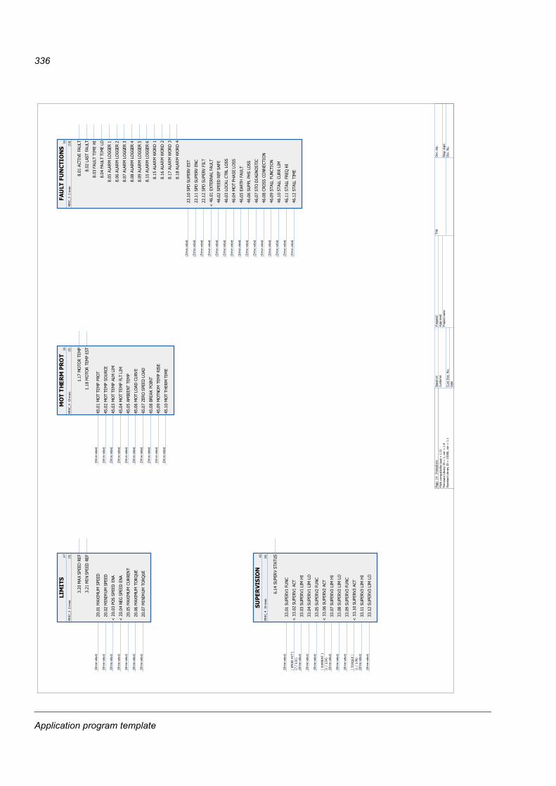
336
LIMIT
S27
MIS
C_3
2 m
sec
(5)
2
0.01
MAX
IMU
M S
PEED
(Driv
e va
lue)
2
0.02
MIN
IMUM
SPE
ED(D
rive
valu
e)
< 2
0.03
PO
S SP
EED
ENA
(Driv
e va
lue)
< 2
0.04
NEG
SPE
ED E
NA(D
rive
valu
e)
2
0.05
MAX
IMU
M C
UR
REN
T(D
rive
valu
e)
2
0.06
MAX
IMU
M T
OR
QUE
(Driv
e va
lue)
2
0.07
MIN
IMUM
TO
RQUE
(Driv
e va
lue)
3.20
MA
X SP
EED
REF
3.21
MIN
SPE
ED R
EF
FAU
LT F
UN
CTI
ON
S33
MIS
C_3
2 m
sec
(10)
22
.10
SPD
SU
PERV
EST
(Driv
e va
lue)
22
.11
SPD
SU
PERV
EN
C(D
rive
valu
e)
22
.12
SPD
SU
PERV
FIL
T(D
rive
valu
e)
< 4
6.01
EXT
ERN
AL
FAU
LT(D
rive
valu
e)
46
.02
SPEE
D R
EF S
AFE
(Driv
e va
lue)
46
.03
LOCA
L CT
RL L
OSS
(Driv
e va
lue)
46
.04
MO
T PH
ASE
LO
SS(D
rive
valu
e)
46
.05
EART
H F
AULT
(Driv
e va
lue)
46
.06
SUPP
L PH
S LO
SS(D
rive
valu
e)
46
.07
STO
DIA
GN
OST
IC(D
rive
valu
e)
46
.08
CRO
SS C
ONN
ECTI
ON
(Driv
e va
lue)
46
.09
STAL
L FU
NCT
ION
(Driv
e va
lue)
46
.10
STAL
L CU
RR L
IM(D
rive
valu
e)
46
.11
STAL
L FR
EQ H
I(D
rive
valu
e)
46
.12
STAL
L TI
ME
(Driv
e va
lue)
8.01
ACT
IVE
FAUL
T
8.02
LAS
T FA
ULT
8.03
FAU
LT T
IME
HI
8.04
FA
ULT
TIM
E LO
8.05
ALA
RM L
OG
GER
1
8.06
ALA
RM L
OG
GER
2
8.07
ALA
RM L
OG
GER
3
8.08
ALA
RM L
OG
GER
4
8.09
ALA
RM L
OG
GER
5
8.10
ALA
RM L
OG
GER
6
8.15
ALA
RM
WO
RD
1
8.16
ALA
RM
WO
RD
2
8.17
ALA
RM
WO
RD
3
8.18
ALA
RM
WO
RD
4
MO
T T
HE
RM
PR
OT
32
MIS
C_4
10
mse
c(5
)
45.0
1 M
OT
TEM
P PR
OT
(Driv
e va
lue)
45.0
2 M
OT
TEM
P SO
URC
E(D
rive
valu
e)
45.0
3 M
OT
TEM
P AL
M L
IM(D
rive
valu
e)
45.0
4 M
OT
TEM
P FL
T LI
M(D
rive
valu
e)
45.0
5 AM
BIEN
T TE
MP
(Driv
e va
lue)
45.0
6 M
OT
LOAD
CU
RVE
(Driv
e va
lue)
45.0
7 ZE
RO S
PEED
LO
AD(D
rive
valu
e)
45.0
8 BR
EAK
POIN
T(D
rive
valu
e)
45.0
9 M
OTN
OM
TEM
P RI
SE(D
rive
valu
e)
45.1
0 M
OT
THER
M T
IME
(Driv
e va
lue)
1.17
MO
TOR
TEM
P
1.18
MO
TOR
TEM
P ES
T
SUP
ERV
ISIO
N45
MIS
C_4
10
mse
c(6
)
3
3.01
SU
PER
V1 F
UN
C(D
rive
valu
e)
< 3
3.02
SU
PERV
1 AC
T[
SPEE
D A
CT ]
(7 /
1.0
1)
3
3.03
SU
PER
V1 L
IM H
I(D
rive
valu
e)
3
3.04
SU
PER
V1 L
IM L
O(D
rive
valu
e)
3
3.05
SU
PER
V2 F
UN
C(D
rive
valu
e)
< 3
3.06
SU
PERV
2 AC
T[
CURR
ENT
](1
/ 1
.04)
3
3.07
SU
PER
V2 L
IM H
I(D
rive
valu
e)
3
3.08
SU
PER
V2 L
IM L
O(D
rive
valu
e)
3
3.09
SU
PER
V3 F
UN
C(D
rive
valu
e)
< 3
3.10
SU
PERV
3 AC
T[
TORQ
UE
](1
/ 1
.06)
3
3.11
SU
PER
V3 L
IM H
I(D
rive
valu
e)
3
3.12
SU
PER
V3 L
IM L
O(D
rive
valu
e)
6.14
SUP
ERV
STAT
US
Page
14
P
rote
ctio
nsFW
A co
mpa
tibili
ty lev
el =
1.5
1Fi
rmw
are
Libr
ary
ID =
1, ve
r =
1.0
Stan
dard
Lib
rary
ID
= 1
0000
, ver
= 1
.1
Base
d on
Cust
omer
Cust
. D
oc. N
o.D
ate
Prep
ared
App
rove
dPr
ojec
t nam
e
Title
Doc
. des
.
Resp
. dep
t.D
oc. N
o.
Application program template
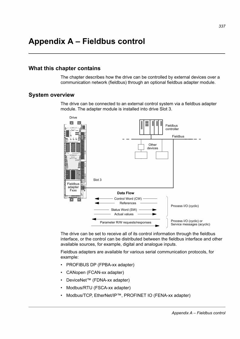
337
Appendix A – Fieldbus control
What this chapter containsThe chapter describes how the drive can be controlled by external devices over a communication network (fieldbus) through an optional fieldbus adapter module.
System overviewThe drive can be connected to an external control system via a fieldbus adapter module. The adapter module is installed into drive Slot 3.
The drive can be set to receive all of its control information through the fieldbus interface, or the control can be distributed between the fieldbus interface and other available sources, for example, digital and analogue inputs.
Fieldbus adapters are available for various serial communication protocols, for example:
• PROFIBUS DP (FPBA-xx adapter)
• CANopen (FCAN-xx adapter)
• DeviceNet™ (FDNA-xx adapter)
• Modbus/RTU (FSCA-xx adapter)
• Modbus/TCP, EtherNet/IP™, PROFINET IO (FENA-xx adapter)
Fieldbus
Otherdevices
Fieldbuscontroller
References
Data Flow
Status Word (SW)Actual values
Parameter R/W requests/responses
Drive
Slot 3
Process I/O (cyclic)
Service messages (acyclic)
Control Word (CW)
Fieldbus adapter
Fxxx
Process I/O (cyclic) or
Appendix A – Fieldbus control
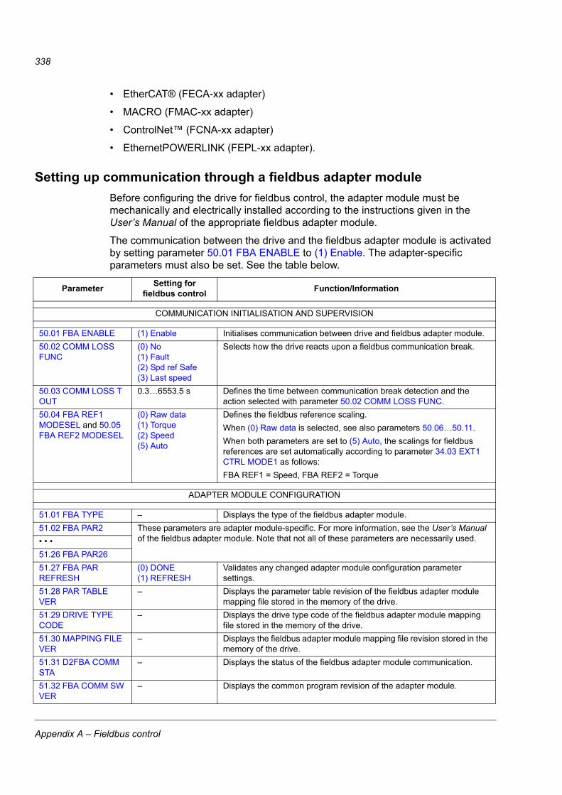
338
• EtherCAT® (FECA-xx adapter)
• MACRO (FMAC-xx adapter)
• ControlNet™ (FCNA-xx adapter)
• EthernetPOWERLINK (FEPL-xx adapter).
Setting up communication through a fieldbus adapter moduleBefore configuring the drive for fieldbus control, the adapter module must be mechanically and electrically installed according to the instructions given in the User’s Manual of the appropriate fieldbus adapter module.
The communication between the drive and the fieldbus adapter module is activated by setting parameter 50.01 FBA ENABLE to (1) Enable. The adapter-specific parameters must also be set. See the table below.
Parameter Setting for fieldbus control Function/Information
COMMUNICATION INITIALISATION AND SUPERVISION
50.01 FBA ENABLE (1) Enable Initialises communication between drive and fieldbus adapter module.50.02 COMM LOSS FUNC
(0) No(1) Fault(2) Spd ref Safe(3) Last speed
Selects how the drive reacts upon a fieldbus communication break.
50.03 COMM LOSS T OUT
0.3…6553.5 s Defines the time between communication break detection and the action selected with parameter 50.02 COMM LOSS FUNC.
50.04 FBA REF1 MODESEL and 50.05 FBA REF2 MODESEL
(0) Raw data(1) Torque(2) Speed(5) Auto
Defines the fieldbus reference scaling.When (0) Raw data is selected, see also parameters 50.06…50.11.When both parameters are set to (5) Auto, the scalings for fieldbus references are set automatically according to parameter 34.03 EXT1 CTRL MODE1 as follows:FBA REF1 = Speed, FBA REF2 = Torque
ADAPTER MODULE CONFIGURATION
51.01 FBA TYPE – Displays the type of the fieldbus adapter module.51.02 FBA PAR2 These parameters are adapter module-specific. For more information, see the User’s Manual
of the fieldbus adapter module. Note that not all of these parameters are necessarily used.• • •51.26 FBA PAR2651.27 FBA PAR REFRESH
(0) DONE(1) REFRESH
Validates any changed adapter module configuration parameter settings.
51.28 PAR TABLE VER
– Displays the parameter table revision of the fieldbus adapter module mapping file stored in the memory of the drive.
51.29 DRIVE TYPE CODE
– Displays the drive type code of the fieldbus adapter module mapping file stored in the memory of the drive.
51.30 MAPPING FILE VER
– Displays the fieldbus adapter module mapping file revision stored in the memory of the drive.
51.31 D2FBA COMM STA
– Displays the status of the fieldbus adapter module communication.
51.32 FBA COMM SW VER
– Displays the common program revision of the adapter module.
Appendix A – Fieldbus control

339
After the module configuration parameters have been set, the drive control parameters (see section Setting the drive control parameters below) must be checked and adjusted when necessary.
The new settings will take effect when the drive is powered up the next time, or when parameter 51.27 FBA PAR REFRESH is activated.
Setting the drive control parametersThe Setting for fieldbus control column gives the value to use when the fieldbus interface is the desired source or destination for that particular signal. The Function/ Information column gives a description of the parameter.
51.33 FBA APPL SW VER
– Displays the application program revision of the adapter module.
Note: In the User’s Manual of the fieldbus adapter module, the parameter group number is 1 or A for parameters 51.01…51.26.
TRANSMITTED DATA SELECTION
52.01 FBA DATA IN1 … 52.12 FBA DATA IN12
04…614…16101…9999
Defines the data transmitted from drive to fieldbus controller.Note: If the selected data is 32 bits long, two parameters are reserved for the transmission.
53.01 FBA DATA OUT1 … 53.12 FBA DATA OUT12
01…311…131001…9999
Defines the data transmitted from fieldbus controller to drive.Note: If the selected data is 32 bits long, two parameters are reserved for the transmission.
Note: In the User’s Manual of the fieldbus adapter module, the parameter group number is 2 or B for parameters 52.01…52.12 and 3 or C for parameters 53.01…53.12.
Parameter Setting for fieldbus control Function/Information
CONTROL COMMAND SOURCE SELECTION
10.01 EXT1 START FUNC
(3) FBA Selects fieldbus as the source for the start and stop commands when EXT1 is selected as the active control location.
10.04 EXT2 START FUNC
(3) FBA Selects fieldbus as the source for the start and stop commands when EXT2 is selected as the active control location.
24.01 SPEED REF1 SEL (3) FBA REF1(4) FBA REF2
Fieldbus reference REF1 or REF2 is used as speed reference 1.
24.02 SPEED REF2 SEL (3) FBA REF1(4) FBA REF2
Fieldbus reference REF1 or REF2 is used as speed reference 2.
32.01 TORQ REF1 SEL (3) FBA REF1(4) FBA REF2
Fieldbus reference REF1 or REF2 is used as torque reference 1.
32.02 TORQ REF ADD SEL
(3) FBA REF1(4) FBA REF2
Fieldbus reference REF1 or REF2 is used for torque reference addition.
SYSTEM CONTROL INPUTS
16.07 PARAM SAVE (0) Done(1) Save
Saves parameter value changes (including those made through fieldbus control) to permanent memory.
Parameter Setting for fieldbus control Function/Information
Appendix A – Fieldbus control
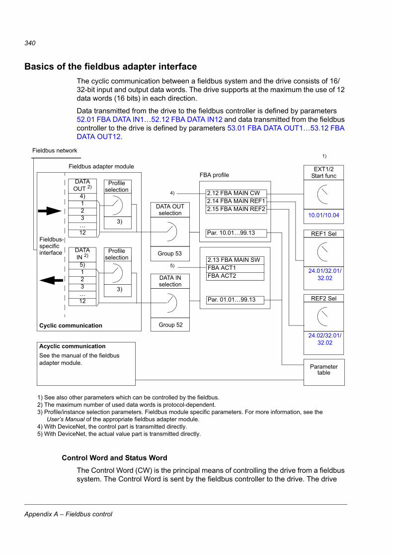
340
Basics of the fieldbus adapter interfaceThe cyclic communication between a fieldbus system and the drive consists of 16/32-bit input and output data words. The drive supports at the maximum the use of 12 data words (16 bits) in each direction.
Data transmitted from the drive to the fieldbus controller is defined by parameters 52.01 FBA DATA IN1…52.12 FBA DATA IN12 and data transmitted from the fieldbus controller to the drive is defined by parameters 53.01 FBA DATA OUT1…53.12 FBA DATA OUT12.
Control Word and Status WordThe Control Word (CW) is the principal means of controlling the drive from a fieldbus system. The Control Word is sent by the fieldbus controller to the drive. The drive
Fieldbus adapter module
Fieldbus-
Fieldbus network
specificinterface
DATAOUT 2)
4)123…12
DATAIN 2)
5)123…12
2.13 FBA MAIN SWFBA ACT1FBA ACT2
Par. 01.01…99.13
2.12 FBA MAIN CW2.14 FBA MAIN REF12.15 FBA MAIN REF2
Par. 10.01…99.13
FBA profile
1) See also other parameters which can be controlled by the fieldbus.2) The maximum number of used data words is protocol-dependent.3) Profile/instance selection parameters. Fieldbus module specific parameters. For more information, see the
User’s Manual of the appropriate fieldbus adapter module.4) With DeviceNet, the control part is transmitted directly.5) With DeviceNet, the actual value part is transmitted directly.
Profileselection
3)
Profileselection
3)
Parameter table
EXT1/2Start func
REF1 Sel
Group 53
DATA OUTselection
Group 52
DATA INselection
4)
5)
1)
Cyclic communication
Acyclic communicationSee the manual of the fieldbus adapter module.
24.01/32.01/32.02
REF2 Sel
24.02/32.01/32.02
10.01/10.04
Appendix A – Fieldbus control

341
switches between its states according to the bit-coded instructions of the Control Word.
The Status Word (SW) is a word containing status information, sent by the drive to the fieldbus controller.
Actual valuesActual values (ACT) are 16/32-bit words containing information on selected operations of the drive.
FBA communication profileThe FBA communication profile is a state machine model which describes the general states and state transitions of the drive. The State diagram on page 342 presents the most important states (including the FBA profile state names). The FBA Control Word (2.12 FBA MAIN CW, page 67) commands the transitions between these states and the FBA Status Word (2.13 FBA MAIN SW, page 69) indicates the status of the drive.
Fieldbus adapter module profile (selected by adapter module parameter) defines how the control word and status word are transmitted in a system which consists of fieldbus controller, fieldbus adapter module and drive. With transparent modes, control word and status word are transmitted without any conversion between the fieldbus controller and the drive. With other profiles (e.g. PROFIdrive for FPBA-01, AC/DC drive for FDNA-01, DS-402 for FCAN-01 and ABB Drives profile for all fieldbus adapter modules) fieldbus adapter module converts the fieldbus-specific control word to the FBA communication profile and status word from FBA communication profile to the fieldbus-specific status word.
For descriptions of other profiles, see the User’s Manual of the appropriate fieldbus adapter module.
Fieldbus referencesReferences (FBA REF) are 16/32-bit signed integers. A negative reference is formed by calculating the two’s complement from the corresponding positive reference value. The contents of each reference word can be used as speed or torque reference.
When torque or speed reference scaling is selected (by parameter 50.04 FBA REF1 MODESEL / 50.05 FBA REF2 MODESEL), the fieldbus references are 32-bit integers. The value consists of a 16-bit integer value and a 16-bit fractional value. The speed/torque reference scaling is as follows:
Reference Scaling NotesTorque reference FBA REF / 65536
(value in %)Final reference is limited by parameters 20.06 MAXIMUM TORQUE and 20.07 MINIMUM TORQUE.
Speed reference FBA REF / 65536(value in rpm)
Final reference is limited by parameters 20.01 MAXIMUM SPEED, 20.02 MINIMUM SPEED and 24.12 SPEED REFMIN ABS.
Appendix A – Fieldbus control

342
State diagramThe following presents the state diagram for the FBA communication profile. For other profiles, see the User’s Manual of the appropriate fieldbus adapter module.
MAINS OFF
Power ON
from any state
FBACommunication
Profile
(FBA SW Bit 0 = 1)
n(f)=0 / I=0
(FBA SW Bit 6 = 1)
(FBA CW Bit 16 = 1)
(FBA CW Bit 0 = 1)
OFF1 (FBA CW Bit 4 = 1
OFF1ACTIVE
C D
(FBA CW Bit 13 = 0)
RUNNING (FBA SW Bit 3 = 1)
(FBA SW Bit 5 = 1)
from any state
from any state
Emergency StopOFF3 (FBA CW Bit 3 = 1
n(f)=0 / I=0
OFF3ACTIVE
Emergency OFFOFF2 (FBA CW Bit 2 = 1
(FBA SW Bit 4 = 1)OFF2ACTIVE
RFG: OUTPUTENABLED
RFG: ACCELERATORENABLED
B
B C D
(FBA CW Bit 12 = 0)
D
(FBA CW Bit 14 = 0)
A
C
FBA CW = Fieldbus Control WordFBA SW = Fieldbus Status Wordn = SpeedI = Input Current
(FBA SW Bit 8 = 1)
RFG = Ramp Function Generatorf = Frequency
D
from any state
Fault
(FBA SW Bit 16 = 1)
(FBA CW Bit 8 = 1)
STARTINHIBITED
(FBA CW Bits 7 = 1)
READY TOSTART
Par. 10.12 = 0
from any state
and FBA CW Bit 0 = 1)
and FBA CW Bit 0 = 1)
and FBA CW Bit 0 = 1)
Par. 10.12 = 1
RUNDISABLEFAULT
OPERATING
(FBA SW Bit 1 = 0)
(FBA CW Bit 7 = 0)
(FBA CW = xxxx xxxx xxxx xxx0 xxxx 1xxx 1xxx xx10)
(FBA CW = xxxx xxxx xxxx xxx0 xxx0 1xxx 1xxx xx10)
(FBA CW = xxxx xxxx xxxx xxx0 xx00 1xxx 1xxx xx10)
(FBA CW = xxxx xxxx xxxx xxx0 x000 1xxx 1xxx xx10)
E
E
Appendix A – Fieldbus control
343
Appendix B – Drive-to-drive link
What this chapter containsThis chapter describes the wiring of, and available communication methods on the drive-to-drive link. Examples of using standard function blocks in the communication are also given starting on page 351.
GeneralThe drive-to-drive link is a daisy-chained RS-485 transmission line, constructed by connecting the X5 terminal blocks of the JCU Control Units of several drives. It is also possible to use an FMBA Modbus extension module installed into an option slot on the JCU. The firmware supports up to 63 nodes on the link.
The link has one master drive; the rest of the drives are followers. By default, the master broadcasts control commands as well as speed and torque references for all followers. The master can send 8 messages per millisecond at 100/150-microsecond intervals. Sending one message takes approximately 15 microseconds, which results in a theoretical link capacity of roughly 6 messages per 100 microseconds.
Multicasting the control data and reference 1 to a pre-defined group of drives is possible, as is chained multicast messaging. Reference 2 is always broadcast by the master to all followers. See parameters 57.11…57.14.
WiringShielded twisted-pair cable (~100 ohm, e.g. PROFIBUS-compatible cable) must be used for the wiring. The maximum length of the link is 50 metres (164 ft).
The JCU Control Unit has a jumper (J3, “T”) next to the X5 terminal block for bus termination. Termination must be ON on the drives at the ends of the drive-to-drive link; on intermediate drives, termination must be OFF.
Instead of the X5 connector, an FMBA Modbus extension module can be used.
For best immunity, high quality cable is recommended. The cable should be kept as short as possible. Unnecessary loops and running the cable near power cables (such as motor cables) must be avoided.
Note: The cable shields are to be grounded to the control cable clamp plate on the drive. Follow the instructions given in the Hardware Manual of the drive.
Appendix B – Drive-to-drive link
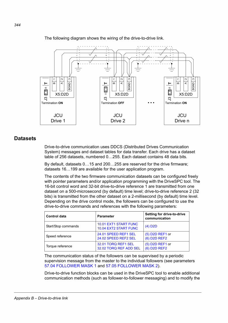
344
The following diagram shows the wiring of the drive-to-drive link.
DatasetsDrive-to-drive communication uses DDCS (Distributed Drives Communication System) messages and dataset tables for data transfer. Each drive has a dataset table of 256 datasets, numbered 0…255. Each dataset contains 48 data bits.
By default, datasets 0…15 and 200…255 are reserved for the drive firmware; datasets 16…199 are available for the user application program.
The contents of the two firmware communication datasets can be configured freely with pointer parameters and/or application programming with the DriveSPC tool. The 16-bit control word and 32-bit drive-to-drive reference 1 are transmitted from one dataset on a 500-microsecond (by default) time level; drive-to-drive reference 2 (32 bits) is transmitted from the other dataset on a 2-millisecond (by default) time level. Depending on the drive control mode, the followers can be configured to use the drive-to-drive commands and references with the following parameters:
The communication status of the followers can be supervised by a periodic supervision message from the master to the individual followers (see parameters 57.04 FOLLOWER MASK 1 and 57.05 FOLLOWER MASK 2).
Drive-to-drive function blocks can be used in the DriveSPC tool to enable additional communication methods (such as follower-to-follower messaging) and to modify the
Control data Parameter Setting for drive-to-drive communication
Start/Stop commands 10.01 EXT1 START FUNC10.04 EXT2 START FUNC (4) D2D
Speed reference 24.01 SPEED REF1 SEL24.02 SPEED REF2 SEL
(5) D2D REF1 or(6) D2D REF2
Torque reference 32.01 TORQ REF1 SEL32.02 TORQ REF ADD SEL
(5) D2D REF1 or(6) D2D REF2
X5:D2D
...
1
TJ3
Termination ON
JCUDrive 1
B
2A
3B
GN
D
X5:D2D
1
J3Termination OFF
JCUDrive 2
B
2A
3B
GN
DT
X5:D2D
1
TJ3
Termination ON
JCUDrive n
B
2A
3B
GN
D
Appendix B – Drive-to-drive link
345
use of datasets between the drives. See the function blocks under Communication (page 258).
Types of messagingEach drive on the link has a unique node address allowing point-to-point communication between two drives. The node address 0 is automatically assigned to the master drive; on other drives, the node address is defined by parameter 57.03 NODE ADDRESS.
Multicast addressing is supported, allowing the composition of groups of drives. Data sent to a multicast address is received by all drives that have that address. A multicast group can consist of 1…62 drives.
In broadcast messaging, data can be sent to all drives (actually, all followers) on the link.
Both master-to-follower(s) and follower-to-follower(s) communication is supported. A follower can send one message to another follower (or a group of followers) after receiving a token message from the master.
Type of messaging NotePoint-to-point Master point-to-point Supported only at master
Read remote Supported only at master
Follower point-to-point Supported only at followers
Standard multicast For both master and followers
Broadcast For both master and followers
Token message for follower-to-follower communication –
Chained multicast Supported only for drive-to-drive reference 1 and control word
Appendix B – Drive-to-drive link
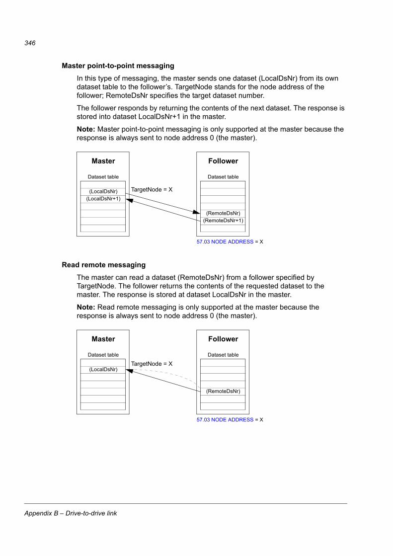
346
Master point-to-point messagingIn this type of messaging, the master sends one dataset (LocalDsNr) from its own dataset table to the follower’s. TargetNode stands for the node address of the follower; RemoteDsNr specifies the target dataset number.
The follower responds by returning the contents of the next dataset. The response is stored into dataset LocalDsNr+1 in the master.
Note: Master point-to-point messaging is only supported at the master because the response is always sent to node address 0 (the master).
Read remote messagingThe master can read a dataset (RemoteDsNr) from a follower specified by TargetNode. The follower returns the contents of the requested dataset to the master. The response is stored at dataset LocalDsNr in the master.
Note: Read remote messaging is only supported at the master because the response is always sent to node address 0 (the master).
Master
Dataset table
(LocalDsNr)(LocalDsNr+1)
TargetNode = X
57.03 NODE ADDRESS = X
Follower
Dataset table
(RemoteDsNr)(RemoteDsNr+1)
Master
Dataset table
(LocalDsNr)TargetNode = X
57.03 NODE ADDRESS = X
Follower
Dataset table
(RemoteDsNr)
Appendix B – Drive-to-drive link
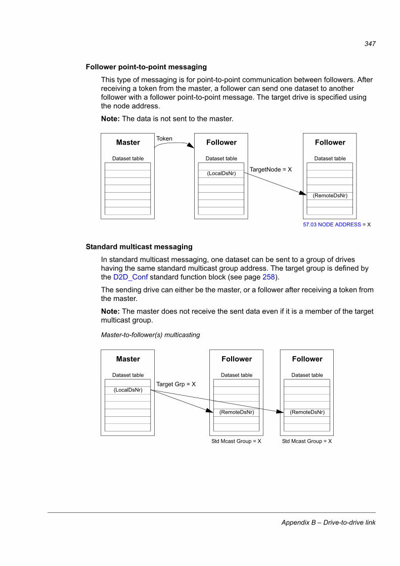
347
Follower point-to-point messagingThis type of messaging is for point-to-point communication between followers. After receiving a token from the master, a follower can send one dataset to another follower with a follower point-to-point message. The target drive is specified using the node address.
Note: The data is not sent to the master.
Standard multicast messagingIn standard multicast messaging, one dataset can be sent to a group of drives having the same standard multicast group address. The target group is defined by the D2D_Conf standard function block (see page 258).
The sending drive can either be the master, or a follower after receiving a token from the master.
Note: The master does not receive the sent data even if it is a member of the target multicast group.
Follower
Dataset table
(LocalDsNr)TargetNode = X
57.03 NODE ADDRESS = X
Follower
Dataset table
(RemoteDsNr)
Master
Dataset table
Token
Follower
Dataset table
(RemoteDsNr)
Target Grp = X
Follower
Dataset table
(RemoteDsNr)
Master
Dataset table
(LocalDsNr)
Master-to-follower(s) multicasting
Std Mcast Group = X Std Mcast Group = X
Appendix B – Drive-to-drive link
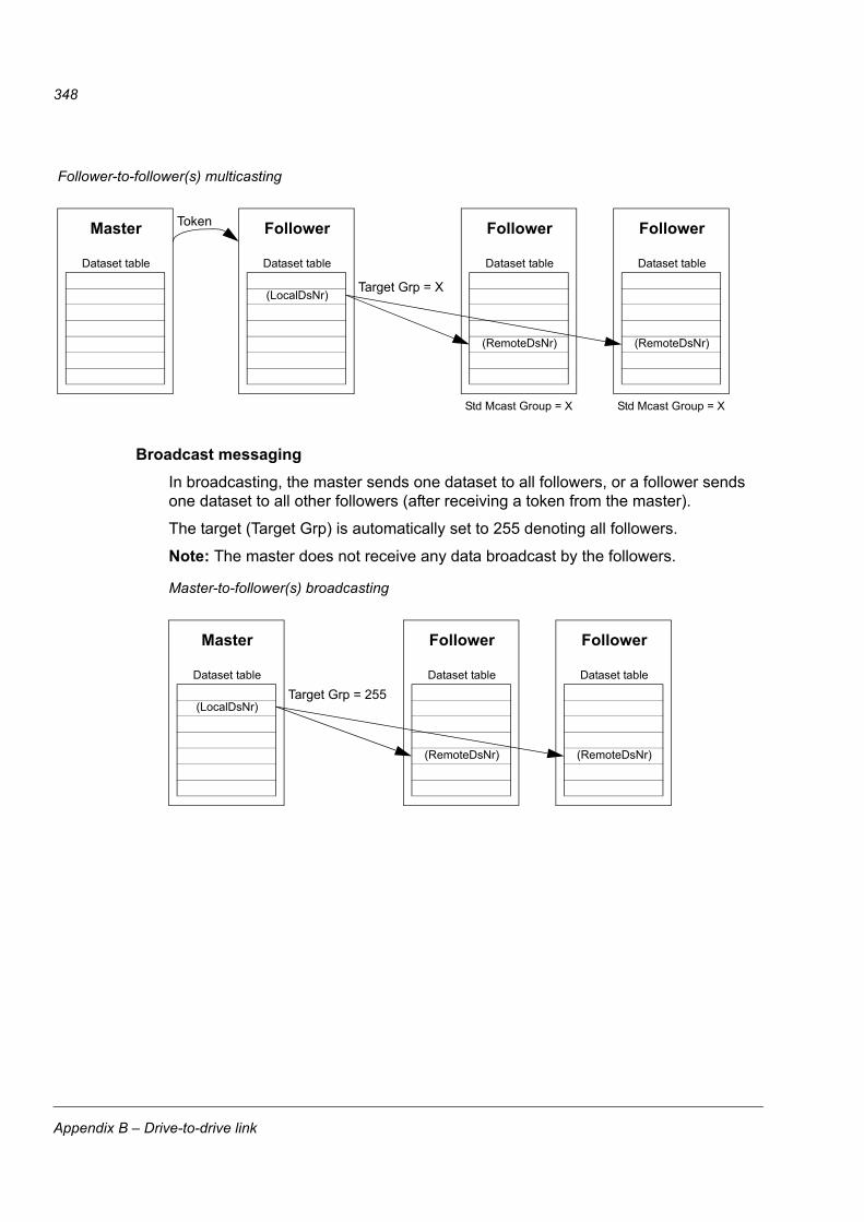
348
Broadcast messagingIn broadcasting, the master sends one dataset to all followers, or a follower sends one dataset to all other followers (after receiving a token from the master).
The target (Target Grp) is automatically set to 255 denoting all followers.
Note: The master does not receive any data broadcast by the followers.
Follower
Dataset table
(RemoteDsNr)
Target Grp = X
Follower
Dataset table
(RemoteDsNr)
Master
Dataset table
Follower-to-follower(s) multicasting
Follower
Dataset table
(LocalDsNr)
Token
Std Mcast Group = X Std Mcast Group = X
Follower
Dataset table
(RemoteDsNr)
Target Grp = 255
Follower
Dataset table
(RemoteDsNr)
Master
Dataset table
(LocalDsNr)
Master-to-follower(s) broadcasting
Appendix B – Drive-to-drive link
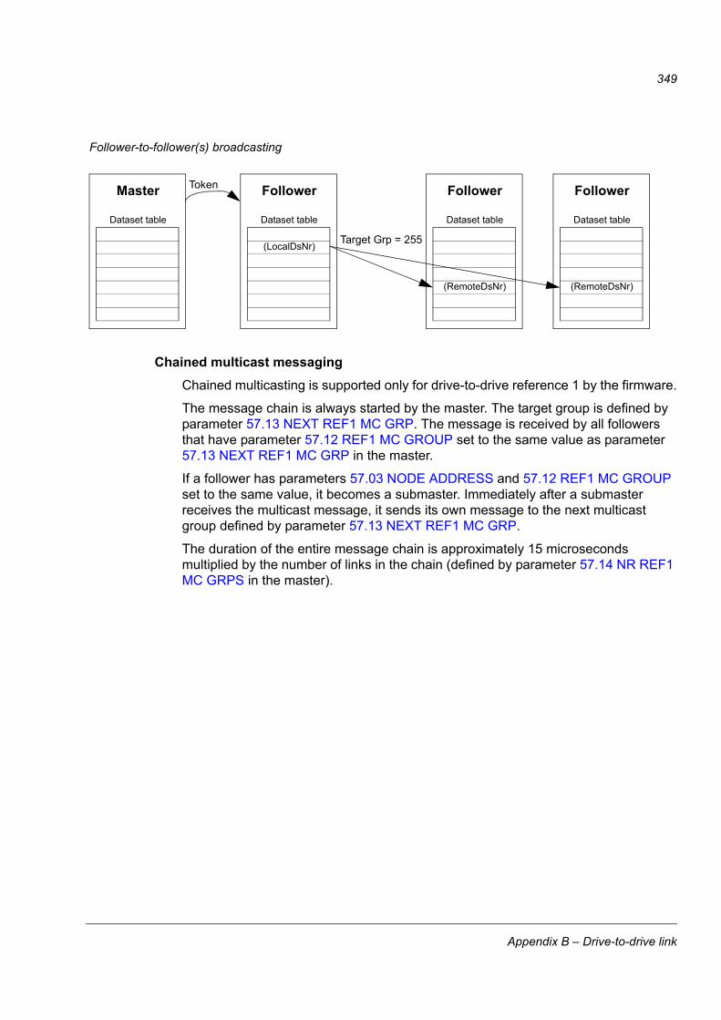
349
Chained multicast messagingChained multicasting is supported only for drive-to-drive reference 1 by the firmware.
The message chain is always started by the master. The target group is defined by parameter 57.13 NEXT REF1 MC GRP. The message is received by all followers that have parameter 57.12 REF1 MC GROUP set to the same value as parameter 57.13 NEXT REF1 MC GRP in the master.
If a follower has parameters 57.03 NODE ADDRESS and 57.12 REF1 MC GROUP set to the same value, it becomes a submaster. Immediately after a submaster receives the multicast message, it sends its own message to the next multicast group defined by parameter 57.13 NEXT REF1 MC GRP.
The duration of the entire message chain is approximately 15 microseconds multiplied by the number of links in the chain (defined by parameter 57.14 NR REF1 MC GRPS in the master).
Follower
Dataset table
(RemoteDsNr)
Target Grp = 255
Follower
Dataset table
(RemoteDsNr)
Master
Dataset table
Follower-to-follower(s) broadcasting
Follower
Dataset table
(LocalDsNr)
Token
Appendix B – Drive-to-drive link
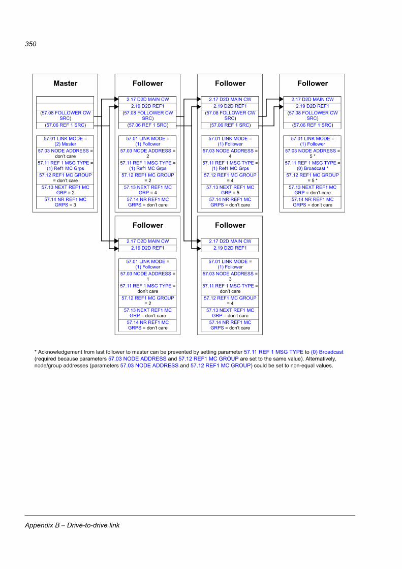
350
Master
(57.08 FOLLOWER CW SRC)
(57.06 REF 1 SRC)
57.01 LINK MODE =(2) Master
57.03 NODE ADDRESS =don’t care
57.11 REF 1 MSG TYPE =(1) Ref1 MC Grps
57.12 REF1 MC GROUP = don’t care
57.13 NEXT REF1 MC GRP = 2
57.14 NR REF1 MC GRPS = 3
Follower
2.17 D2D MAIN CW2.19 D2D REF1
57.01 LINK MODE =(1) Follower
57.03 NODE ADDRESS =1
57.11 REF 1 MSG TYPE =don’t care
57.12 REF1 MC GROUP = 2
57.13 NEXT REF1 MC GRP = don’t care
57.14 NR REF1 MC GRPS = don’t care
Follower
2.17 D2D MAIN CW2.19 D2D REF1
(57.08 FOLLOWER CW SRC)
(57.06 REF 1 SRC)
57.01 LINK MODE =(1) Follower
57.03 NODE ADDRESS =2
57.11 REF 1 MSG TYPE =(1) Ref1 MC Grps
57.12 REF1 MC GROUP = 2
57.13 NEXT REF1 MC GRP = 4
57.14 NR REF1 MC GRPS = don’t care
Follower
2.17 D2D MAIN CW2.19 D2D REF1
57.01 LINK MODE =(1) Follower
57.03 NODE ADDRESS =3
57.11 REF 1 MSG TYPE =don’t care
57.12 REF1 MC GROUP = 4
57.13 NEXT REF1 MC GRP = don’t care
57.14 NR REF1 MC GRPS = don’t care
Follower
2.17 D2D MAIN CW2.19 D2D REF1
(57.08 FOLLOWER CW SRC)
(57.06 REF 1 SRC)
57.01 LINK MODE =(1) Follower
57.03 NODE ADDRESS =4
57.11 REF 1 MSG TYPE =(1) Ref1 MC Grps
57.12 REF1 MC GROUP = 4
57.13 NEXT REF1 MC GRP = 5
57.14 NR REF1 MC GRPS = don’t care
Follower
2.17 D2D MAIN CW2.19 D2D REF1
(57.08 FOLLOWER CW SRC)
(57.06 REF 1 SRC)
57.01 LINK MODE =(1) Follower
57.03 NODE ADDRESS =5 *
57.11 REF 1 MSG TYPE =(0) Broadcast *
57.12 REF1 MC GROUP = 5 *
57.13 NEXT REF1 MC GRP = don’t care
57.14 NR REF1 MC GRPS = don’t care
* Acknowledgement from last follower to master can be prevented by setting parameter 57.11 REF 1 MSG TYPE to (0) Broadcast (required because parameters 57.03 NODE ADDRESS and 57.12 REF1 MC GROUP are set to the same value). Alternatively, node/group addresses (parameters 57.03 NODE ADDRESS and 57.12 REF1 MC GROUP) could be set to non-equal values.
Appendix B – Drive-to-drive link

351
Examples of using standard function blocks in drive-to-drive communication
See also the descriptions of the drive-to-drive function blocks starting on page 258.
Example of master point-to-point messaging
Master Follower (node 1)
1. The master sends a constant (1) and the value of the message counter into follower dataset 20. Data is prepared to and sent from dataset 16.
2. The follower sends the received counter value and a constant (21) as a reply to the master.
3. The master calculates the difference of the latest message number and received data.
Appendix B – Drive-to-drive link
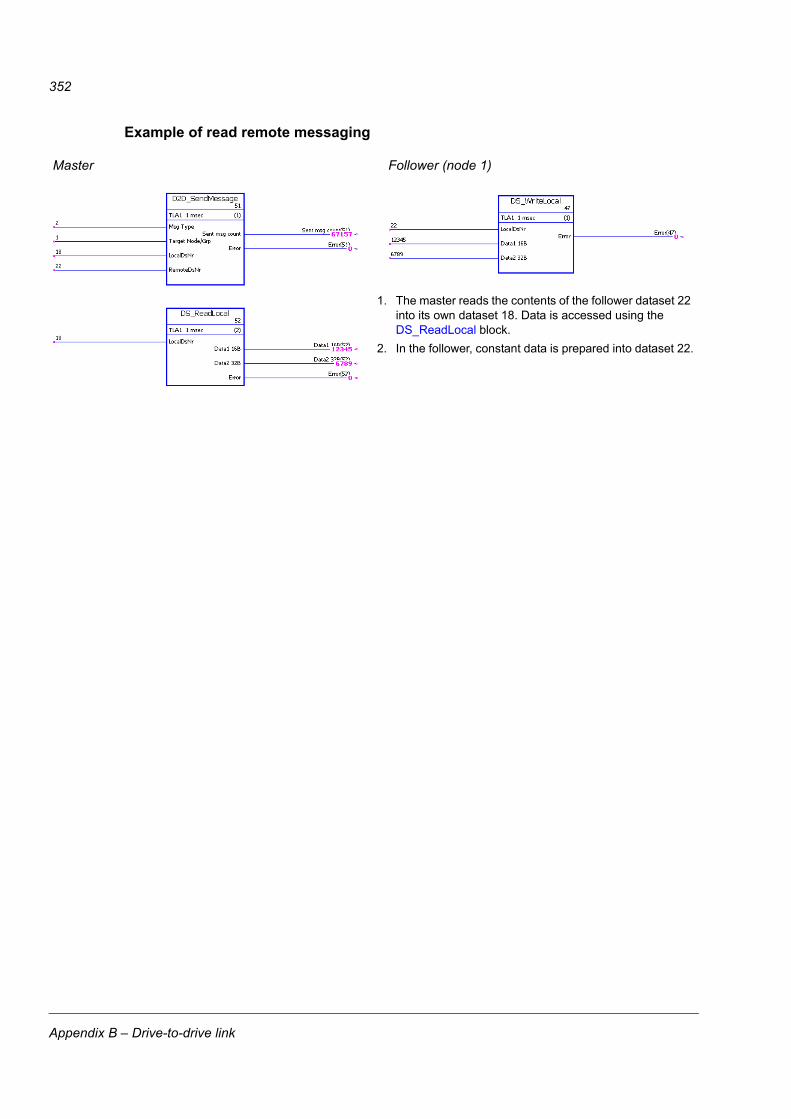
352
Example of read remote messaging
Master Follower (node 1)
1. The master reads the contents of the follower dataset 22 into its own dataset 18. Data is accessed using the DS_ReadLocal block.
2. In the follower, constant data is prepared into dataset 22.
Appendix B – Drive-to-drive link
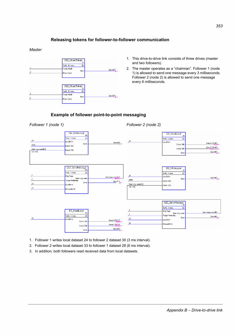
353
Releasing tokens for follower-to-follower communication
Example of follower point-to-point messaging
Master
1. This drive-to-drive link consists of three drives (master and two followers).
2. The master operates as a “chairman”. Follower 1 (node 1) is allowed to send one message every 3 milliseconds. Follower 2 (node 2) is allowed to send one message every 6 milliseconds.
Follower 1 (node 1) Follower 2 (node 2)
1. Follower 1 writes local dataset 24 to follower 2 dataset 30 (3 ms interval).2. Follower 2 writes local dataset 33 to follower 1 dataset 28 (6 ms interval).3. In addition, both followers read received data from local datasets.
Appendix B – Drive-to-drive link
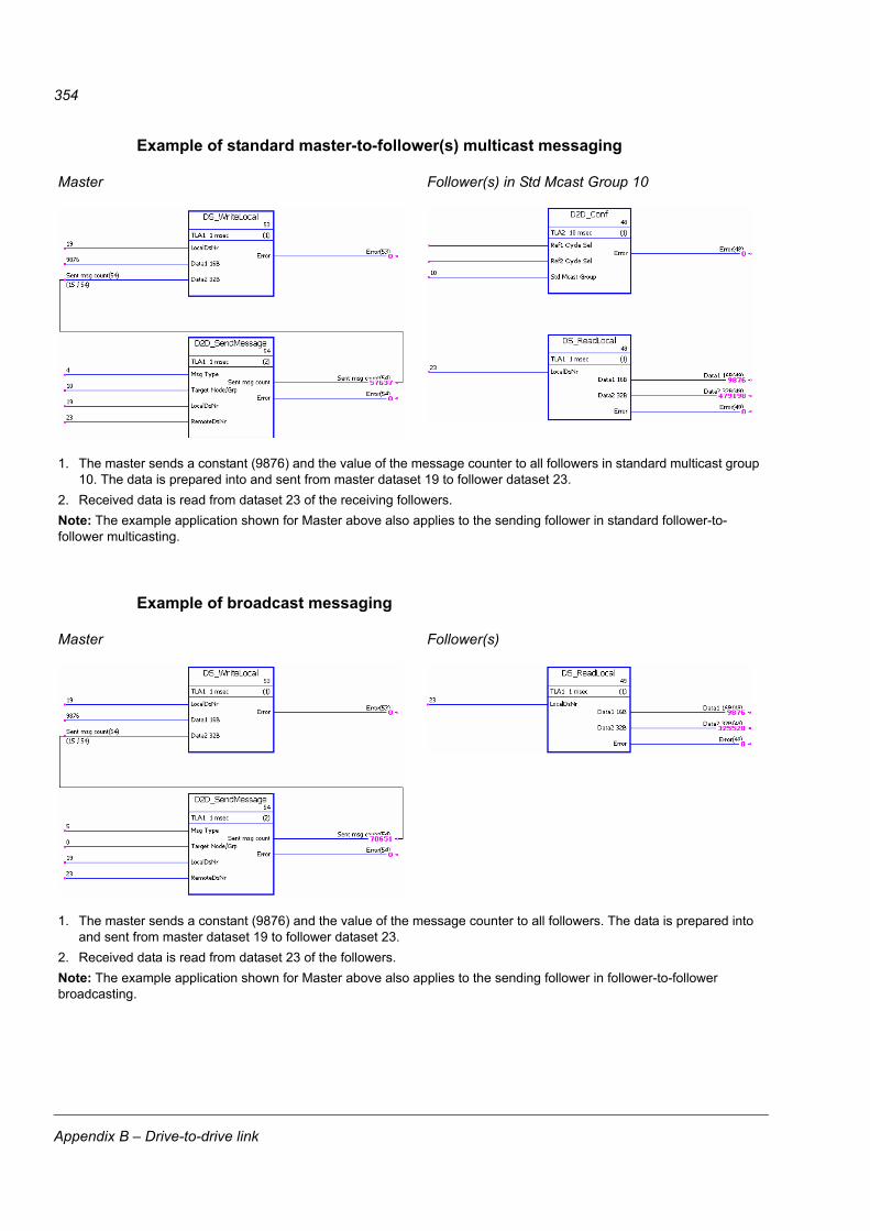
354
Example of standard master-to-follower(s) multicast messaging
Example of broadcast messaging
Master Follower(s) in Std Mcast Group 10
1. The master sends a constant (9876) and the value of the message counter to all followers in standard multicast group 10. The data is prepared into and sent from master dataset 19 to follower dataset 23.
2. Received data is read from dataset 23 of the receiving followers.Note: The example application shown for Master above also applies to the sending follower in standard follower-to-follower multicasting.
Master Follower(s)
1. The master sends a constant (9876) and the value of the message counter to all followers. The data is prepared into and sent from master dataset 19 to follower dataset 23.
2. Received data is read from dataset 23 of the followers.Note: The example application shown for Master above also applies to the sending follower in follower-to-follower broadcasting.
Appendix B – Drive-to-drive link
355
Appendix C – Control chain and drive logic diagrams
What this chapter containsThis chapter presents the drive control chain and logic.
Appendix C – Control chain and drive logic diagrams
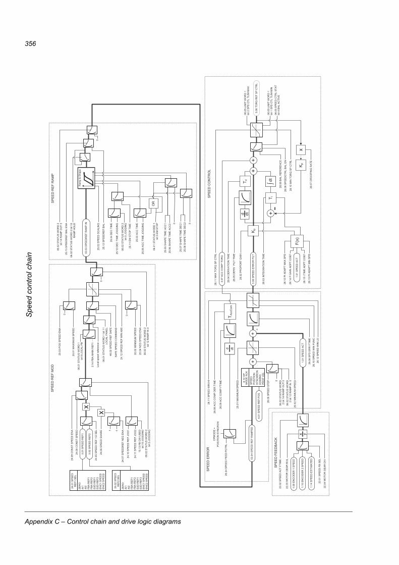
356
SP
EE
D E
RR
OR
SP
EE
D C
ON
TRO
L
SP
EE
D R
EF
RA
MP
3.01
SP
EE
D R
EF1
3.02
SP
EE
D R
EF2
24.0
5 S
PE
ED
RE
F 1/
2 S
EL
24.0
6 S
PE
ED
SH
AR
E
24.0
7 S
PE
ED
RE
F N
EG
EN
A1 -1
24.0
9 C
ON
ST
SP
EE
D E
NA
24.1
0 S
PE
ED
RE
F JO
G1
24.1
1 S
PE
ED
RE
F JO
G2
10.1
3 FB
CW
US
ED
bit 1
0 JO
GG
ING
06.0
2 S
TATU
S W
OR
D 2
bit 5
JO
GG
ING
24.0
8 C
ON
ST
SP
EE
D
SP
EE
D R
EF
MO
D
20.0
3 P
OS
SP
EE
D E
NA
0
20.0
2 M
INIM
UM
SP
EE
D
20.0
4 N
EG
SP
EE
D E
NA
0
06.0
2 S
TATU
S W
OR
D 2
bi
t 12
RA
MP
IN 0
Loca
l spe
ed re
fere
nce
06.0
1 S
TATU
S W
OR
D 1
bit
11
LOC
AL
PA
NE
L46
.02
SP
EE
D R
EF
SA
FE
SA
FE S
PE
ED
CO
MM
AN
D
06.0
1 S
TATU
S W
OR
D 1
bi
t 9 L
OC
AL
FB
0
20.0
1 M
AX
IMU
M S
PE
ED
2.14
FB
A M
AIN
RE
F1
24.1
2 S
PE
ED
RE
F M
IN A
BS
3.07
AC
C C
OM
P T
OR
Q
Kp
T i
T d
Kp
28.0
4 D
ER
IVA
TIO
N T
IME
28.0
5 D
ER
IV F
ILT
TIM
E
28.0
2 P
RO
PO
RT
GA
IN
28.0
7 D
RO
OP
ING
RA
TE
28.0
8 B
AL
RE
FER
EN
CE
28.0
3 IN
TEG
RA
TIO
N T
IME
3.08
TO
RQ
RE
F S
P C
TRL
28.1
1 M
AX
TO
RQ
SP
CTR
L
28.1
0 M
IN T
OR
Q S
P C
TRL
28.0
9 S
PE
ED
CTR
L B
AL
EN
++
+d dt
�dt
x
28.1
4 P
GA
IN A
DP
T C
OE
F
28.1
5 I T
IME
AD
PT
CO
EF
28.1
2 P
I AD
AP
T M
AX
SP
D
28.1
3 P
I AD
AP
T M
IN S
PD
1.01
SP
EE
D A
CT
F(x)
06.0
5 LI
MIT
WO
RD
1bi
t 1 S
PD
CTL
TLI
M M
IN
06.0
5 LI
MIT
WO
RD
1bi
t 2 S
PD
CTL
TLI
M M
AX
06.0
5 S
PE
ED
CTR
L S
TAT
bit 4
BA
L A
CTI
VE
3.06
SP
EE
D E
RR
OR
FIL
T
26.0
5 S
PE
ED
STE
P
26.0
6 S
PD
ER
R F
TIM
E
20.0
1 M
AX
IMU
M S
PE
ED
20.0
2 M
INIM
UM
SP
EE
D
T Acc
Com
26.0
8 A
CC
CO
MP
DE
R T
IME
26.0
9 A
CC
CO
MP
FTI
ME
d dt
006
.02
STA
TUS
WO
RD
2
bit 1
4 R
AM
P O
UT
006
.02
STA
TUS
WO
RD
2 bi
t 12
RA
MP
IN 0
+-
26.1
0 S
PE
ED
WIN
FU
NC
26.1
1 S
PE
ED
WIN
HI
26.1
2 S
PE
ED
WIN
LO
4.01
SP
EE
D R
EF
PO
S
26.0
4 S
PE
ED
FE
ED
PC
TRL
22.0
4 M
OTO
R G
EA
R D
IV
22.0
3 M
OTO
R G
EA
R M
UL
22.0
2 S
PE
ED
AC
T FT
IME
22.0
1 S
PE
ED
FB
SE
L
1.14
SP
EE
D E
STI
MA
TED
1.08
EN
CO
DE
R 1
SP
EE
D
1.10
EN
CO
DE
R 2
SP
EE
D1.
01 S
PE
ED
AC
T
OP
MO
DE
=
PO
SIT
ION
SY
NC
RO
N
x y
03.0
4 S
PE
ED
RE
F R
AM
PE
DS
PE
ED
PO
SIT
ION
SY
NC
HR
ON
HO
MIN
GP
RO
F V
EL
6.12
OP
M
OD
E A
CK
+
0
Ram
p &
Sha
pe
03.0
3 S
PE
ED
RE
F R
AM
P IN
25.0
2 S
PE
ED
SC
ALI
NG
25.0
3 A
CC
TIM
E
25.0
4 D
EC
TIM
E
25.0
5 S
HA
PE
TIM
E A
CC
1
25.0
6 S
HA
PE
TIM
E A
CC
2
25.0
7 S
HA
PE
TIM
E D
EC
1
25.0
8 S
HA
PE
TIM
E D
EC
2
25.1
0 D
EC
TIM
E J
OG
GIN
G
25.1
1 E
M S
TOP
TIM
E
25.1
2 S
PE
ED
RE
F B
AL
25.1
3 S
PE
ED
RE
F B
AL
EN
A
25.0
9 A
CC
TIM
E J
OG
GIN
G 0
06.0
1 S
TATU
S W
OR
D 1
bi
t 5 E
M S
TOP
06.0
2 S
TATU
S W
OR
D 2
bit 5
JO
GG
ING
OR
06.0
2 S
TATU
S W
OR
D 2
bi
t 14
RA
MP
OU
T 0
06.0
2 S
TATU
S W
OR
D 2
bit
13
RA
MP
HO
LD
0
SP
EE
D F
EE
DB
AC
K
ZER
OA
I1A
I2FB
A R
EF1
FBA
RE
F2D
2D R
EF1
D2D
RE
F2E
NC
1 S
PE
ED
EN
C2
SP
EE
D
24.0
1 S
PE
ED
R
EF1
SE
L
ZER
OA
I1A
I2FB
A R
EF1
FBA
RE
F2D
2D R
EF1
D2D
RE
F2E
NC
1 S
PE
ED
EN
C2
SP
EE
D
24.0
2 S
PE
ED
R
EF2
SE
L
Spe
ed c
ontro
l cha
in
Appendix C – Control chain and drive logic diagrams
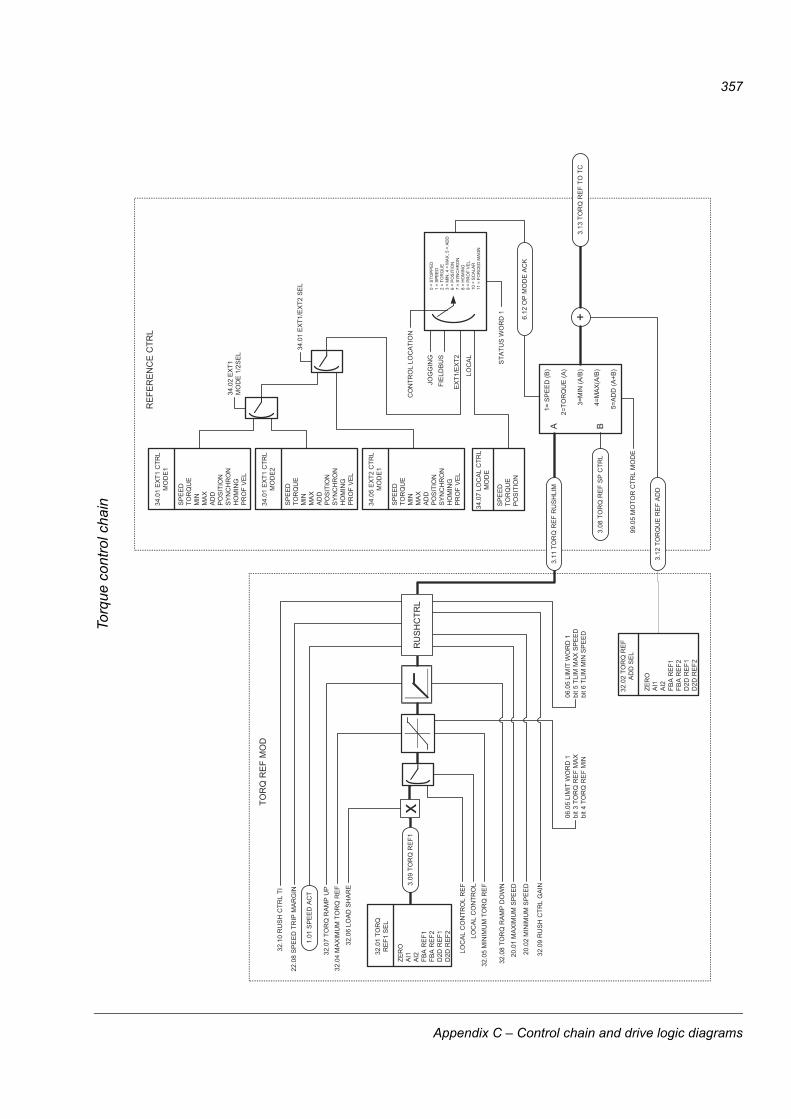
357
LOC
AL
CO
NTR
OL
LOC
AL C
ON
TRO
L R
EF
32.0
6 LO
AD S
HA
RE
32.0
4 M
AXIM
UM
TO
RQ
RE
F
32.0
5 M
INIM
UM
TO
RQ
REF
32.0
7 TO
RQ
RA
MP
UP
32.0
8 TO
RQ
RA
MP
DO
WN
22.0
8 S
PEE
D T
RIP
MAR
GIN
1.01
SPE
ED
AC
T
20.0
1 M
AXIM
UM
SP
EED
20.0
2 M
INIM
UM
SP
EED
06.0
5 LI
MIT
WO
RD
1bi
t 5 T
LIM
MAX
SP
EE
Dbi
t 6 T
LIM
MIN
SP
EED
06.0
5 LI
MIT
WO
RD
1bi
t 3 T
OR
Q R
EF
MA
Xbi
t 4 T
OR
Q R
EF
MIN
1= S
PE
ED
(B)
2=TO
RQ
UE
(A)
3=M
IN (A
/B)
4=M
AX(A
/B)
5=AD
D (A
+B)
3.08
TO
RQ
RE
F S
P C
TRL
99.0
5 M
OTO
R C
TRL
MO
DE
+3.
13 T
OR
Q R
EF
TO T
C
34.0
2 EX
T1
MO
DE
1/2
SEL
SPE
ED
TOR
QU
EP
OS
ITIO
N
34.0
7 LO
CA
L C
TRL
MO
DE
34.0
1 E
XT1/
EXT2
SE
L
SPE
EDTO
RQ
UE
MIN
MA
XAD
DPO
SIT
ION
SYN
CH
RO
NH
OM
ING
PRO
F V
EL
34.0
1 EX
T1 C
TRL
MO
DE
1
SPE
EDTO
RQ
UE
MIN
MA
XAD
DPO
SIT
ION
SYN
CH
RO
NH
OM
ING
PRO
F V
EL
34.0
1 EX
T1 C
TRL
MO
DE
2
3.09
TO
RQ
RE
F1ZE
RO
AI1
AI2
FBA
RE
F1FB
A R
EF2
D2D
REF
1D
2D R
EF2
32.0
1 TO
RQ
R
EF1
SE
L
3.11
TO
RQ
RE
F R
US
HLI
M
6.12
OP
MO
DE
AC
K
3.12
TO
RQ
UE
RE
F AD
DZE
RO
AI1
AI2
FBA
REF
1FB
A R
EF2
D2D
REF
1D
2D R
EF2
32.0
2 TO
RQ
RE
F A
DD
SE
L
TOR
Q R
EF
MO
D
RE
FER
EN
CE
CTR
L
0 =
STO
PPE
D1
= S
PEE
D2
= TO
RQ
UE
3 =
MIN
, 4 =
MAX
,5 =
AD
D6
= P
OS
ITIO
N7
= S
YNC
HR
ON
8 =
HO
MIN
G9
= P
RO
F VE
L10
= S
CAL
AR
11 =
FO
RC
ED M
AGN
STA
TUS
WO
RD
1
CO
NTR
OL
LOC
ATIO
N
JOG
GIN
GFI
ELD
BUS
LOC
AL
EX
T1/E
XT2
SPE
EDTO
RQ
UE
MIN
MA
XAD
DPO
SIT
ION
SYN
CH
RO
NH
OM
ING
PRO
F V
EL
34.0
5 EX
T2 C
TRL
MO
DE
1
A B
RU
SHC
TRL
32.0
9 R
USH
CTR
L G
AIN
32.1
0 R
USH
CTR
L TI
Torq
ue c
ontro
l cha
in
Appendix C – Control chain and drive logic diagrams

358
34.0
1 E
XT1
/EX
T2 S
EL
DR
IVE
LO
GIC
EX
T S
TAR
T
10.1
5 JO
G E
NA
BLE
10.0
9 R
UN
EN
AB
LE
10.0
8 FA
ULT
RE
SE
T10
.12
STA
RT
INH
IBIT
06.0
2 S
TATU
S W
OR
D 2
06.0
1 S
TATU
S W
OR
D 1
02.1
8 D
2D F
OLL
OW
ER
CW
D2D
CO
MM
UN
ICA
TIO
N
57.0
1 LI
NK
MO
DE
57.0
2 C
OM
M L
OS
S F
UN
C
57.0
3 N
OD
E A
DD
R
57.0
5 FO
LLO
WE
R M
AS
K2
57.0
4 FO
LLO
WE
R M
AS
K1
57.0
6 R
EF1
SR
C57
.07
RE
F2 S
RC
MA
STE
R
57.0
8 FO
LLO
WE
R C
W S
RC
57.0
9 K
ER
NE
L S
YN
C M
OD
E
57.1
0 K
ER
NE
L S
YN
C O
FFS
KE
RN
EL
SY
NC
57.1
1 R
EF1
MS
G T
YP
E57
.12
RE
F1 M
C G
RP
MU
LTIC
AS
T / C
HA
IN C
OM
M
57.1
3 N
EX
T R
EF1
MC
GR
P
57.1
4 N
R R
EF1
MC
GR
PS
CO
MM
ON
SE
TTIN
GS
FOLL
OW
ER
S
2.17
D2D
MA
IN C
W
2.19
D2D
RE
F12.
20 D
2D R
EF2
IN1
3-W
IRE
FBA
*D
2DIN
1F IN
2RIN
1S IN
2DIR
10.0
1 E
XT1
S
TAR
T FU
NC
IN1
3-W
IRE
FBA
*D
2DIN
1F IN
2RIN
1S IN
2DIR
10.0
4 E
XT2
S
TAR
T FU
NC
10.0
7 JO
G S
TAR
T 1
10.1
4 JO
G S
TAR
T 2
10.1
7 S
TAR
T E
NA
BLE
11.0
1 S
TAR
T M
OD
E
11.0
3 S
TOP
MO
DE
OR
10.1
0 E
M S
TOP
OFF
310
.11
EM
STO
P O
FF1
* S
EE
FB
A P
ICTU
RE
EM
STO
P
OFF
1/O
FF2/
OFF
3
STA
TE M
AC
HIN
E
DIS
AB
LE
STO
PP
ED
RU
NN
ING
FAU
LTE
D
NO
RM
AL
STO
P R
AM
P/
CO
AS
TE
XT
STO
P
LOC
AL
MO
DE
PC
/ P
anel
LOC
STA
RT
Driv
e lo
gic
1
Appendix C – Control chain and drive logic diagrams
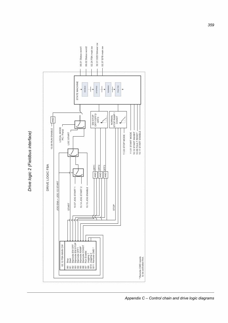
359
DR
IVE
LO
GIC
FB
A
10.1
5 JO
G E
NA
BLE
10.0
8 FA
ULT
RE
SE
T10
.12
STA
RT
INH
IBIT
NO
RM
AL
STO
P R
AM
P /
CO
AS
T
STA
TE M
AC
HIN
E
DIS
AB
LE
STO
PP
ED
RU
NN
ING
FAU
LTE
D
10.0
7 JO
G S
TAR
T 1
10.1
4 JO
G S
TAR
T 2
10.1
7 S
TA
RT
EN
AB
LE
11.0
1 S
TAR
T M
OD
E
AN
DO
FF1
OFF
2
OFF
3
AN
D
AN
D
* R
emot
e C
MD
nee
ds
to b
e ac
tivat
ed fi
rst.
EM
ST
OP
O
FF1
/OFF
2/O
FF3
11.0
3 S
TOP
MO
DE
STA
RT
LOC
AL
MO
DE
PC
/ P
anel
B0
S
top
B1
S
tart
B2
S
tpm
ode
EM
OFF
B3
S
tpm
ode
EM
STO
PB
4
Stp
mod
e O
FF1
B5
S
tpm
ode
RA
MP
B6
S
tpm
ode
CO
AS
TB
7
Run
Ena
ble
B9
Jo
ggin
g 1
B10
Jog
ging
2B
11 R
emot
e C
MD
*
02.1
2 FB
A M
AIN
CW
LOC
STA
RT
10.0
9 R
UN
EN
AB
LE
STO
P
AN
D
JOG
EN
A +
JO
G 1
/2 S
TA
RT
06.0
2 S
tatu
s w
ord2
06.0
1 S
tatu
s w
ord1
02.3
1 D
2D fo
llow
er c
w
02.2
4 F
BA
mai
n sw
02.3
7 E
FB m
ain
sw
Driv
e lo
gic
2 (F
ield
bus
inte
rface
)
Appendix C – Control chain and drive logic diagrams
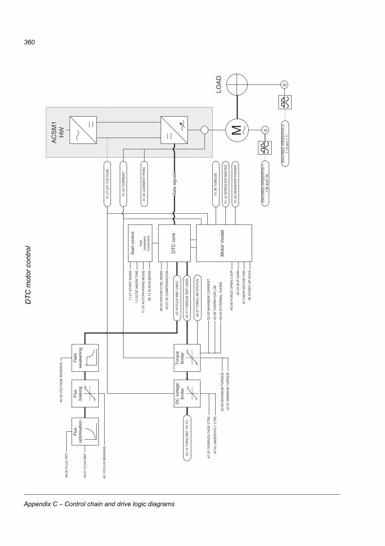
360
01.0
4 C
UR
RE
NT
01.0
5 C
UR
RE
NT
PE
RC
01.0
6 TO
RQ
UE
01.0
7 D
C-V
OLT
AG
E
01.1
4 S
PE
ED
ES
TIM
ATE
D
Gat
e si
gnal
s
20.0
8 TH
ER
M C
UR
LIM
20.0
6 M
AX
IMU
M T
OR
QU
E
20.0
7 M
INIM
UM
TO
RQ
UE
DC
vol
tage
lim
iter
Sta
rt co
ntro
l
Fast
Aut
omat
icC
onst
tim
e
11.0
1 S
TAR
T M
OD
E
11.0
2 D
C M
AG
N T
IME
40.0
1 FL
UX
RE
F
20.0
5 M
AX
IMU
M C
UR
RE
NT
Mot
or m
odel
11.0
7 A
UTO
PH
AS
ING
MO
DE
99.1
3 ID
RU
N M
OD
E
01.2
2 IN
VE
RTE
R P
OW
ER
40.0
6 FO
RC
E O
PE
N L
OO
P
40.0
3 S
LIP
GA
IN
97 U
SE
R M
OTO
R P
AR
99 S
TAR
T-U
P D
ATA
47.0
1 O
VE
RV
OLT
AG
E C
TRL
47.0
2 U
ND
ER
VO
LT C
TRL
99.0
5 M
OTO
R C
TRL
MO
DE
95.0
2 E
XTE
RN
AL
CH
OK
E
40.0
7 IR
CO
MP
EN
SA
TIO
N
40.0
4 V
OLT
AG
E R
ES
ER
VE
DTC
cor
e
40.0
5 FL
UX
OP
T
Torq
ue
limite
r
Fiel
d w
eake
ning
Flux
br
akin
gFl
ux
optim
isat
ion
03.1
6 FL
UX
RE
F U
SE
D
03.1
7 TO
RQ
UE
RE
F U
SE
D
06.0
7 TO
RQ
LIM
STA
TUS
03.1
3 TO
RQ
RE
F TO
TC
E
AC
SM
1 H
W
EN
CO
RE
D S
PE
ED
/PO
S 1
1.
08 a
nd1.
09
EN
CO
RE
D S
PE
ED
/PO
S 2
1.
10 a
nd 1
.11
LOA
D
E
40.1
0 FL
UX
BR
AK
ING
DTC
mot
or c
ontro
l
Appendix C – Control chain and drive logic diagrams

3AFE
6884
8261
RE
V G
/ E
NE
FFE
CTI
VE
: 201
1-09
-30
ABB OyDrivesP.O. Box 184FI-00381 HELSINKIFINLANDTelephone +358 10 22 11Fax +358 10 22 22681www.abb.com/drives
ABB Inc.Automation TechnologiesDrives & Motors16250 West Glendale DriveNew Berlin, WI 53151USATelephone 262 785-3200
1-800-HELP-365Fax 262 780-5135www.abb.com/drives
ABB Beijing Drive Systems Co. Ltd.No. 1, Block D, A-10 Jiuxianqiao BeiluChaoyang DistrictBeijing, P.R. China, 100015Telephone +86 10 5821 7788Fax +86 10 5821 7618www.abb.com/drives