energy and buildings - download.xuebalib.comdownload.xuebalib.com/xuebalib.com.33018.pdf ·...
TRANSCRIPT

Ss
Ya
Hb
c
2d
a
ARRA
KSVTSAT
1
aaaatp
iwdmnibc[
sT
0h
Energy and Buildings 66 (2013) 545–552
Contents lists available at ScienceDirect
Energy and Buildings
j ourna l ho me page: www.elsev ier .com/ locate /enbui ld
imulation of smart windows in the ZnO/VO2/ZnS sandwichedtructure with improved thermochromic properties
uan Zhaoa, Rui Xub, Xuanru Zhangc, Xiang Huc, Randall J. Knized, Yalin Lua,c,d,∗
CAS Key Laboratory of Materials for Energy Conversion, Department of Materials Science and Engineering, University of Science and Technology of China,efei 230026, PR ChinaDepartment of Optics and Optical Engineering, University of Science and Technology of China, Hefei 230026, PR ChinaAdvanced Applied Research Center, Hefei National Laboratory for Physical Sciences at the Microscale, University of Science and Technology of China, Anhui30026, PR ChinaLaser Optics Research Center, Physics Department, United States Air Force Academy, CO 80840, USA
r t i c l e i n f o
rticle history:eceived 16 January 2013eceived in revised form 25 June 2013ccepted 24 July 2013
a b s t r a c t
We modeled a sandwiched structure ZnO/VO2/ZnS potentially as a VO2-based smart window with a goalto increase both luminous transmittance (Tlum) and solar modulation ability (�Tsol). Compared to the pre-viously used single-layer antireflection coating, the new sandwiched structure broadens the reflectanceminimum in the visible light range and enlarges the transmission gap in the near-infrared (NIR) region,when switching between the semiconducting and the metallic states and when utilizing an intermediate
eywords:mart windowanadium dioxideransparent materialandwichntireflection
index ZnS layer imbedded between the VO2 film and substrate. The 3/4-1/4-3/4 wavelength–thicknessmodel exhibited a high solar modulation ability (�Tsol = 13.01%), and maintained a high Tlum at 63.24%and 57.39% both in semiconducting and metallic phases, respectively.
© 2013 Elsevier B.V. All rights reserved.
hin film
. Introduction
Excessive energy consumption in buildings, transportations,nd other industries have led to growing concerns on using renew-ble energy and energy saving, which are two increasing importantspects of the economy sustainable development [1,2]. Particularttention on energy saving in buildings and man-made construc-ions should be paid, since it consumes as much as 30–40% of therimary energy in the world [1,3].
One efficient way to make an effective use of solar energyn buildings is to modulate sunlight transmission through glass
indows by solar-controlling coatings, also called “smart win-ows” [4,5]. Chromogenic materials based smart windows canodulate the amount of solar irradiation in response to the exter-
al stimulus intelligently [5,6]. Common chromogenic materialsnclude electrochromic thin films varying their optical properties
y electrical voltage or discharging [7–11], photochromic onesoloring under ultraviolet irradiation or bleaching in the dark12,13] and thermochromic ones changing solar light transmission∗ Corresponding author at: CAS Key Laboratory of Materials for Energy Conver-ion, Department of Materials Science and Engineering, University of Science andechnology of China, Hefei 230026, PR China. Tel.: +86 0551 3603004.
E-mail addresses: [email protected], [email protected] (Y. Lu).
378-7788/$ – see front matter © 2013 Elsevier B.V. All rights reserved.ttp://dx.doi.org/10.1016/j.enbuild.2013.07.071
depending on the temperature [14–23]. Among them, the ther-mochromic smart windows, typically based on vanadium dioxide(VO2), have been attracting particular research interests roughlydue to the below three aspects. Firstly, VO2 has a rapid responseto the environmental temperature, switching between a near-infrared (NIR) transparent semiconducting state and an opaquemetallic state [14,22]. Secondly, during the phase transition,ultraviolet light is almost fully absorbed while the transmissionof visible light remains almost unaffected [16,24]. Thirdly, thesemiconducting-metallic phase transition temperature (Tc) couldbe reduced almost to room temperature by doping [25,26], or byreducing crystal sizes [27], from its normal phase–transition tem-perature of ∼68 ◦C [28].
However, due to VO2’s high reflectance and strong absorptionresulting from its high refractive index (RI) and large absorp-tion coefficient, low luminous transmittance (Tlum) and insufficientsolar modulation ability (�Tsol) retard the practical application ofVO2-based smart windows [14,16]. The main fabrication methodsfor VO2 films include chemical vapor deposition [29], sputter-ing deposition [15], pulsed laser deposition [30], polymer-assisteddeposition [22,24], and so on.
In order to improve Tlum and �Tsol, people have reported thatinvolving an additional antireflection layer could improve thetransmittance in set wavelength [22,31,32]. Unfortunately, con-current improvement on both Tlum and �Tsol is still a challenge.
5 d Buildings 66 (2013) 545–552
FbaivwNi
Zstldvg�cssotThamlwapw
2
di[
n
wtdr
w
T
T
wa(As
T
(o
�
46 Y. Zhao et al. / Energy an
or example, a TiO2 antireflection layer was employed in the VO2-ased smart window [22], by using the destructive interferencend reducing the interface reflectance. However, the improvementn Tlum is weak as it produced a narrow transmittance dip in theisible light region. It only improved the transmittance in a narrowavelength range. In fact, enlarging the transmittance gap in theIR region for two states is needed in order to further explore an
mprovement on �Tsol.In this work, we introduced a sandwiched structure
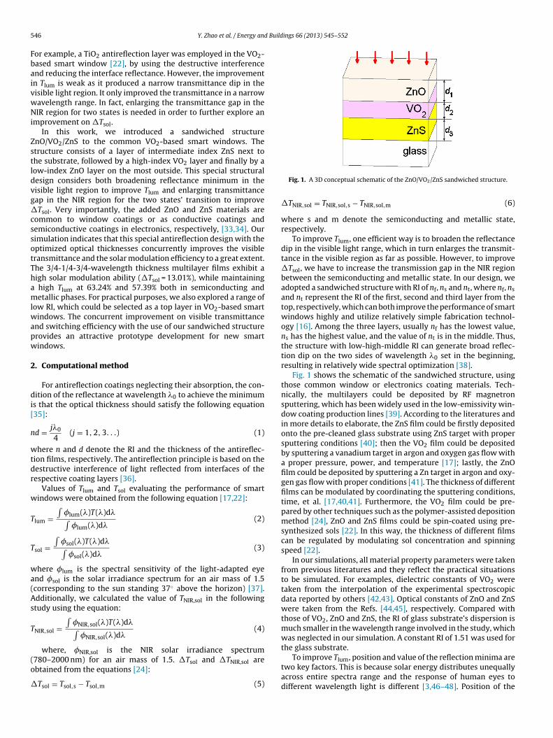
nO/VO2/ZnS to the common VO2-based smart windows. Thetructure consists of a layer of intermediate index ZnS next tohe substrate, followed by a high-index VO2 layer and finally by aow-index ZnO layer on the most outside. This special structuralesign considers both broadening reflectance minimum in theisible light region to improve Tlum and enlarging transmittanceap in the NIR region for the two states’ transition to improveTsol. Very importantly, the added ZnO and ZnS materials are
ommon to window coatings or as conductive coatings andemiconductive coatings in electronics, respectively, [33,34]. Ourimulation indicates that this special antireflection design with theptimized optical thicknesses concurrently improves the visibleransmittance and the solar modulation efficiency to a great extent.he 3/4-1/4-3/4-wavelength thickness multilayer films exhibit aigh solar modulation ability (�Tsol = 13.01%), while maintaining
high Tlum at 63.24% and 57.39% both in semiconducting andetallic phases. For practical purposes, we also explored a range of
ow RI, which could be selected as a top layer in VO2-based smartindows. The concurrent improvement on visible transmittance
nd switching efficiency with the use of our sandwiched structurerovides an attractive prototype development for new smartindows.
. Computational method
For antireflection coatings neglecting their absorption, the con-ition of the reflectance at wavelength �0 to achieve the minimum
s that the optical thickness should satisfy the following equation35]:
d = j�0
4(j = 1, 2, 3. . .) (1)
here n and d denote the RI and the thickness of the antireflec-ion films, respectively. The antireflection principle is based on theestructive interference of light reflected from interfaces of theespective coating layers [36].
Values of Tlum and Tsol evaluating the performance of smartindows were obtained from the following equation [17,22]:
lum =∫
�lum(�)T(�)d�∫
�lum(�)d�(2)
sol =∫
�sol(�)T(�)d�∫
�sol(�)d�(3)
here �lum is the spectral sensitivity of the light-adapted eyend �sol is the solar irradiance spectrum for an air mass of 1.5corresponding to the sun standing 37◦ above the horizon) [37].dditionally, we calculated the value of TNIR,sol in the followingtudy using the equation:
NIR,sol =∫
�NIR,sol(�)T(�)d�∫
�NIR,sol(�)d�(4)
where, � is the NIR solar irradiance spectrum
NIR,sol780–2000 nm) for an air mass of 1.5. �Tsol and �TNIR,sol arebtained from the equations [24]:Tsol = Tsol,s − Tsol,m (5)
Fig. 1. A 3D conceptual schematic of the ZnO/VO2/ZnS sandwiched structure.
�TNIR,sol = TNIR,sol,s − TNIR,sol,m (6)
where s and m denote the semiconducting and metallic state,respectively.
To improve Tlum, one efficient way is to broaden the reflectancedip in the visible light range, which in turn enlarges the transmit-tance in the visible region as far as possible. However, to improve�Tsol, we have to increase the transmission gap in the NIR regionbetween the semiconducting and metallic state. In our design, weadopted a sandwiched structure with RI of nf, ns and nt, where nf, ns
and nt represent the RI of the first, second and third layer from thetop, respectively, which can both improve the performance of smartwindows highly and utilize relatively simple fabrication technol-ogy [16]. Among the three layers, usually nf has the lowest value,ns has the highest value, and the value of nt is in the middle. Thus,the structure with low-high-middle RI can generate broad reflec-tion dip on the two sides of wavelength �0 set in the beginning,resulting in relatively wide spectral optimization [38].
Fig. 1 shows the schematic of the sandwiched structure, usingthose common window or electronics coating materials. Tech-nically, the multilayers could be deposited by RF magnetronsputtering, which has been widely used in the low-emissivity win-dow coating production lines [39]. According to the literatures andin more details to elaborate, the ZnS film could be firstly depositedonto the pre-cleaned glass substrate using ZnS target with propersputtering conditions [40]; then the VO2 film could be depositedby sputtering a vanadium target in argon and oxygen gas flow witha proper pressure, power, and temperature [17]; lastly, the ZnOfilm could be deposited by sputtering a Zn target in argon and oxy-gen gas flow with proper conditions [41]. The thickness of differentfilms can be modulated by coordinating the sputtering conditions,time, et al. [17,40,41]. Furthermore, the VO2 film could be pre-pared by other techniques such as the polymer-assisted depositionmethod [24], ZnO and ZnS films could be spin-coated using pre-synthesized sols [22]. In this way, the thickness of different filmscan be regulated by modulating sol concentration and spinningspeed [22].
In our simulations, all material property parameters were takenfrom previous literatures and they reflect the practical situationsto be simulated. For examples, dielectric constants of VO2 weretaken from the interpolation of the experimental spectroscopicdata reported by others [42,43]. Optical constants of ZnO and ZnSwere taken from the Refs. [44,45], respectively. Compared withthose of VO2, ZnO and ZnS, the RI of glass substrate’s dispersion ismuch smaller in the wavelength range involved in the study, whichwas neglected in our simulation. A constant RI of 1.51 was used forthe glass substrate.
To improve Tlum, position and value of the reflection minima aretwo key factors. This is because solar energy distributes unequallyacross entire spectra range and the response of human eyes todifferent wavelength light is different [3,46–48]. Position of the

Y. Zhao et al. / Energy and Build
Fig. 2. Simulated transmittance spectra for TiO2/VO2 double-layered film in semi-conducting (solid lines) and metallic (broken lines) phases, the red lines aresto
rAlpamfi�auVflttimcfawdtuaa
aifRcclwqe
wrtmaleT
imulated results and the blue lines are data from Ref. [22]. (For interpretation ofhe references to color in this figure legend, the reader is referred to the web versionf this article.)
eflection minimum determines directly the transmittance peak. small shift in transmission peak can change Tlum obviously a
ot. Moreover, the reflection minimum can reflect the transmissionroperty as the absorption is determined mainly by the materi-ls themselves [22]. Particularly, both of them can be tuned byodulating the thickness of each layer inside the structure. In the
ollowing designs, we adopt the wavelength �0 550 nm for predict-ng the thickness of antireflection layer, because both of �lum andsol are high at this wavelength [37]. At 550 nm, the RI of ZnO, VO2nd ZnS were 1.93, 3.27 and 2.37 [42–45], respectively. Here, wese the RI of the semiconducting VO2 to calculate the thickness ofO2 film due to the semiconducting phase having better antire-ection effect [15,16,22]. The simulations were performed usinghe commercial software Comsol Multiphysics, which implementshe finite element method (FEM) to solve Maxwell’s equations ands a widely accepted method in optics [49,50]. For modeling the
ultilayer structures with two infinite horizontal dimensions, theomputational domain was considered as a single unit cell. Per-ectly matched layer (PML) absorbing boundary conditions weredopted in the vertical direction and periodic boundary conditionsere adopted in the horizontal direction [51]. The light was inci-ent to the film surface and the transmittance was calculated fromhe electromagnetic field distributions. Because the solar light isn-polarized, the overall structure response can be treated as theverage of the contributions of transverse magnetic polarized lightnd transverse electric polarized light [50].
For a three-layered structure, the reflectance minimum can bechieved by adjusting the thickness or the RI of each layer as shownn Eq. (1). Moreover, different RI and thickness of materials satis-ying the requirement can attain different reflectance minima asI and thickness form a trade off when confirming �0 [52]. The RIould be modulated by changing both materials and the depositiononditions [22]. Thickness of the films could be controlled by regu-ating deposition condition or time [22,24]. In our structure designs,
e adopted the quarter-quarter-quarter-waved structure and theuarter-half-quarter-waved structure via tuning the thickness ofach layer and maintaining the RI of the used materials unchanged.
In order to confirm the feasibility of our simulation method,e compare our simulation results with the experimental data
eported in Ref. [22] by using the same structure and filmhicknesses. Fig. 2 presents the simulated and experimental trans-
ission spectra for the TiO2/VO2 double-layered structure. Solid
nd broken lines represent VO2 in the semiconducting and metal-ic phase, while red and blue lines represent simulated results andxperimental results, respectively. In both case, the thickness ofiO2 and VO2 films are 55 nm and 210 nm, respectively.ings 66 (2013) 545–552 547
It is clear that the changing trend of wavelength-dependenttransmittance is consistent with the experimental data in Ref. [22].Our transmissions are slightly higher than the reported experimen-tal results in the NIR region, which is considered to be caused bymuch stronger reflection at interfaces. However, this has almostno affect on both Tlum and �Tsol as the simulated spectra andexperimental spectra overlap in the visible light region very well,and that the �Tsol equals to the difference between Tsol,s andTsol,m. Therefore, it enables us to use the optical parameters of thematerials to practically predict the optical behavior of the smartwindows.
3. Results and discussion
3.1. The quarter-quarter-quarter-waved structure and the Tlumimprovement
Firstly, we simulated the optical properties of the quarter-quarter-quarter-waved structure. Fig. 3 shows both transmittanceand reflectance spectra for a bare VO2 film and ZnO/VO2/ZnSthree-layered film with a quarter-quarter-quarter-waved struc-ture both in VO2 semiconducting and metallic phases. Solid andbroken lines represent VO2 in the semiconducting and metal-lic phase, while red and blue lines represent bare VO2 film andZnO/VO2/ZnS three-layered structure, respectively. Both of theVO2 layer has equal thickness of 42 nm. Here, we take ZnO as anantireflection layer due to its stability and relatively lower opticalconstant [44]. Apparently, the transmittance in both semiconduct-ing and metallic phases is improved by a large margin owing to thereduction of reflectance. This structure has a good antireflectionefficiency. In detail, the 42 nm-thick VO2 film has a maximum in thereflectance spectrum at around 530 nm, whereas for ZnO/VO2/ZnSfilms, it appears a minimum reflectance at around 630 nm. Thedeviation of the reflectance minimum from �0 was due to theexistence of the extinction coefficient. The integrated luminous,solar and NIR solar transmittance and their modulation duringSMT are summarized in Table 1. As shown in Table 1, Tlum isremarkably improved, but �Tsol is too small to ensure practicalapplications.
3.2. The quarter-half-quarter-waved structure and the �Tsolimprovement
In order to improve �Tsol, we studied the quarter-half-quarter-waved structure in the following using relatively thick VO2 film.Fig. 4 shows both transmittance and reflectance spectra for a bareVO2 film and ZnO/VO2/ZnS three-layered film with a quarter-half-quarter-waved structure in semiconducting and metallic phases.Red and blue lines represent bare VO2 film and ZnO/VO2/ZnS three-layered structure, while the solid and broken lines stand for VO2in the semiconducting and metallic state, respectively. Similarly,the transmittances have an obvious improvement when comparedwith bare 84 nm VO2 film. It was attributed to a further reduc-tion on the reflectance, though 84 nm-thick VO2 film alone hasa self-antireflection function as shown in Fig. 4b. The quarter-half-quarter-waved ZnO/VO2/ZnS film structure has two reflectionminima on the either side of �0. The one on the left side at 550 nmcan improve Tlum, while the right one at 820 nm can improve �Tsol,thus leading to an increase of �Tsol to 14.94%. This is because theright reflectance dip influences transmittance weakly to the metal-lic VO2 as the absorbance playing a key role in the metallic phase.
However, in this structure, the 84 nm-thick VO2 has greater absorp-tion than 42 nm-thick VO2 film in visible light, leading to the valueof Tlum too small to apply practically. Thinner VO2 film is moresuitable for antireflection exploration.
548 Y. Zhao et al. / Energy and Buildings 66 (2013) 545–552
Fig. 3. Transmittance (a) and reflectance (b) spectra for a bare VO2 film (red lines) and ZnO/VO2/ZnS three-layered film (blue lines) with a quarter-quarter-quarter-wavedstructure in semiconducting (solid lines) and metallic (broken lines) phases, the thickness of ZnO, VO2 and ZnS are 71, 42 and 57 nm, respectively. (For interpretation of thereferences to color in this figure legend, the reader is referred to the web version of this article.)
Table 1Optical and SMT properties for a bare VO2 film and TM/VO2/ZnS films with different structures, ‘e’ stands for experimental results and ‘s’ for the simulation, respectively.
Structure Optical thickness Tlum (%) Tsol (%) �Tsol (%) TNIR,sol (%) �TNIR,sol (%)
S M S M S M
TiO2–VO2 [22] ‘e’ 58.00 53.90 54.30 43.40 10.90 – – –SiO2–VO2 [22] ‘e’ 50.60 52.10 54.40 47.20 7.20 – – –AZO–VO2 [24] ‘e’ – 52.00 52.30 51.30 45.20 6.10 – – –TiO2–VO2–FTO [31] ‘e’ 44.00 38.20 54.40 47.20 8.81 – – –SiO2/Pt/VO2 [32] ‘e’ 37.90 – – – – – – –VO2 films [6] ‘s’ 40.00 34.20 31.12 21.20 9.92 – – –
VO2 �0/4 32.81 34.88 39.54 36.63 2.91 51.13 40.44 10.69�0/2 32.90 26.44 32.07 22.56 9.51 37.09 21.02 16.07
ZnO/VO2/ZnS �0/4-�0/4-�0/4 66.71 58.79 59.05 54.14 4.91 59.66 55.82 3.84�0/4-�0/2-�0/4 42.72 33.20 48.20 32.26 15.94 57.39 34.37 23.023�0/4-�0/4-�0/4 65.31 58.94 56.26 45.60 10.66 62.23 46.30 15.93�0/4-�0/4-3�0/4 66.58 59.32 59.77 50.19 9.58 64.71 50.12 14.593�0/4-�0/4-3�0/4 63.24 57.39 56.67 43.66 13.01 68.59 42.04 26.55
ITO/VO2/ZnS 3�0/4-�0/4-3�0/4 62.21 56.25 55.84 43.31 12.53 66.74 41.53 25.2155.58.56.
3i
tdir
Fsr
IZO/VO2/ZnS 3�0/4-�0/4-3�0/4 63.32 57.46
TiO2/VO2/ZnS 3�0/4-�0/4-3�0/4 64.57 58.87
Ti2O3/VO2/ZnS 3�0/4-�0/4-3�0/4 63.54 57.69
.3. The quarter-3-quarter-quarter-waved structure and dualmprovement of Tlum and �Tsol
Considering the two situations referred above, we realized that
o improve Tlum and �Tsol simultaneously, one effective way is toesign a structure that can form two main antireflection peaks bothn the visible wavelength range and the short-wave NIR wavelengthange, because most of the solar energy is distributed in the visible
ig. 4. Transmittance (a) and reflectance (b) spectra for a bare VO2 film (red lines) andtructure in semiconducting (solid lines) and metallic (broken lines) phases, the thickneseferences to color in this figure legend, the reader is referred to the web version of this a
27 42.46 12.81 66.59 41.11 25.4819 44.54 13.65 70.19 43.53 26.6617 42.89 13.28 67.78 41.55 26.23
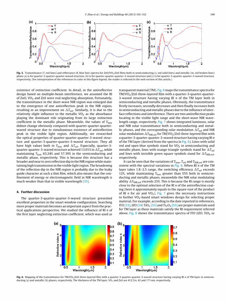
(380–780 nm) and the short-wave NIR (780–1100 nm) regions. Forthis purpose, a 3-times quarter-waved optical thickness of ZnO filmwas designed. Fig. 5a shows the transmittance and reflectance spec-tra of ZnO/VO2/ZnS films with quarter-3-quarter-quarter-waved
structured both in semiconducting and metallic phases. It can beseen that the antireflection peak didnot fall in the correspond-ing �0 and 3�0, which is because the optical constants of ZnO,VO2 and ZnS films were wavelength-dependent and due to theZnO/VO2/ZnS three-layered film (blue lines) with a quarter-half-quarter-waveds of ZnO, VO2 and ZnS are 71, 84 and 57 nm, respectively. (For interpretation of therticle.)
Y. Zhao et al. / Energy and Buildings 66 (2013) 545–552 549
Fig. 5. Transmittance (T, red lines) and reflectance (R, blue line) spectra for ZnO/VO2/ZnS films both in semiconducting (s, red solid lines) and metallic (m, red broken lines)p r-quar reader
edottrrpcdwptthqmmbtogfim
4
emtt
Fd
hase (a) is for quarter-3-quarter-quarter-waved structure, (b) is for quarter-quarteespectively. (For interpretation of the references to color in this figure legend, the
xistence of extinction coefficient. In detail, in the antireflectiveesign based on multiple-beam interference, we assumed the RIf ZnO, VO2 and ZnS were real neglecting absorption. Fortunately,he transmittance in the short-wave NIR region was enlarged dueo the emergence of one antireflection peak in the NIR region,esulting in an improvement on �Tsol. Similarly, it is due to theelatively slight influence to the metallic VO2 as the absorbancelaying the dominant role originating from its large extinctionoefficient in the metallic phase. Meanwhile, the values of Tlumidnot change obviously compared with quarter-quarter-quarter-aved structure due to simultaneous existence of antireflectioneak in the visible light region. Additionally, we researchedhe optical properties of quarter-quarter-quarter-3-waved struc-ure and quarter-3-quarter-quarter-3-waved structure. They allave high values both in Tlum and �Tsol. Especially, quarter-3-uarter-quarter-3-waved structure achieved 13.01% in �Tsol, whileaintaining Tlum 63.24% and 57.39% in the semiconducting andetallic phase, respectively. This is because this structure has a
roader and near to zero reflection dip in the NIR region while main-aining high transmission in the visible light region. The broadeningf the reflection dip in the NIR region is probably due to the leakyuide character at such a thin film, which also means that the con-nement of energy or electromagnetic field in NIR wavelength isuch weaker than that in visible wavelength [35].
. Further discussion
The quarter-3-quarter-quarter-3-waved structure presented
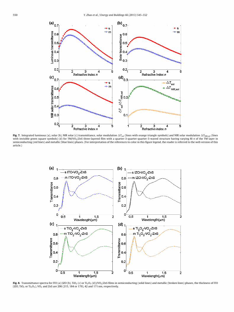
xcellent properties in the smart window configuration. Searchingore proper materials becomes an important aspect from the prac-ical applications perspective. We studied the influence of RI n ofhe first layer neglecting extinction coefficient, which was used as
ig. 6. Mapping of the transmittance for TM/VO2/ZnS three-layered film with a quarter-ucting (a) and metallic (b) phases, respectively. The thickness of the TM layer, VO2 and Z
rter-3-waved structure and (c) is for quarter-3-quarter-quarter-3-waved structure, is referred to the web version of this article.)
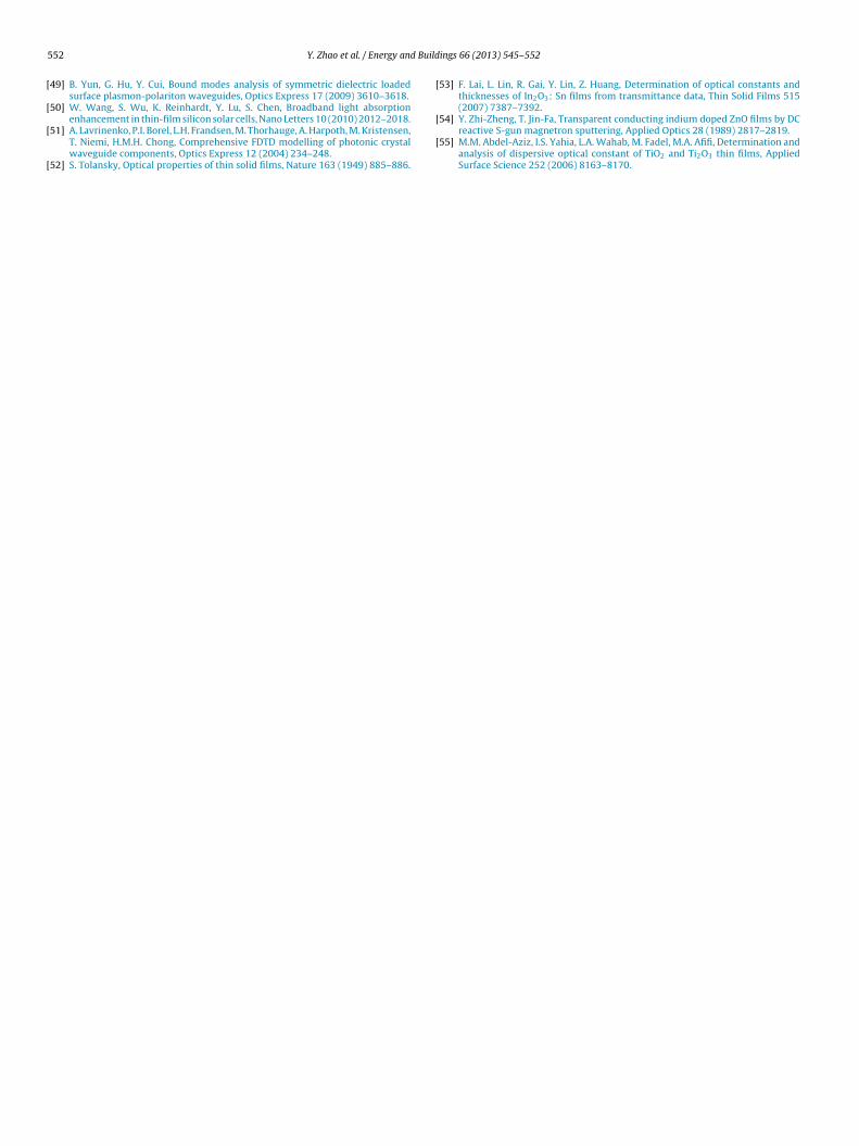
transparent material (TM). Fig. 6 maps the transmittance spectra forTM/VO2/ZnS three-layered film with a quarter-3-quarter-quarter-3-waved structure having varying RI n of the TM layer both insemiconducting and metallic phases. Obviously, the transmittancefirstly increases, secondly decreases and then finally increases bothin semiconducting and metallic phases due to the influence of inter-face reflections and interference. There are two antireflection peakslocating in the visible light range and the short-wave NIR wave-length range, respectively. Fig. 7 shows integrated luminous, solarand NIR solar transmittance both in semiconducting and metal-lic phases, and the corresponding solar modulation �Tsol and NIRsolar modulation �TNIR,sol for TM/VO2/ZnS three-layered film witha quarter-3-quarter-quarter-3-waved structure having varying RI nof the TM layer (derived from the spectra in Fig. 6). Lines with solidred and open blue symbols stand for VO2 in semiconducting andmetallic phase, lines with orange triangle symbols stand for �Tsoland lines with invisible green square symbols stand for �TNIR,sol,respectively.
It can be seen that the variations of Tlum, Tsol and TNIR,sol are con-sistent with the spectral variations in Fig. 6. When RI n of the TMlayer takes 1.8–2.5 range, the switching efficiency �Tsol exceeds12%, while maintaining Tlum greater than 55% both in semicon-ducting and metallic phases, meanwhile the NIR solar modulatingability �TNIR,sol exceeds 25%. This is because the RI range is mostlyclose to the optimal selection of the RI n of the antireflection coat-ing (here it approximately equals to the square root of the productof RI n for air and VO2). Fig. 7 gives the necessary instructionsto further VO2-based smart windows design for selecting proper
material. For example, according to the date reported in references,ITO [53], IZO [54] TiO2 [55] and Ti2O3 [55] are proper materials usedfor TM layer as these materials satisfy the RI requirement referredabove. Fig. 8 shows the transmittance spectra of ITO (IZO, TiO2 or3-quarter-quarter-3-waved structure having varying RI n of TM layer in semicon-nS are 412.5/n, 42 and 171 nm, respectively.
550 Y. Zhao et al. / Energy and Buildings 66 (2013) 545–552
Fig. 7. Integrated luminous (a), solar (b), NIR solar (c) transmittance, solar modulation �Tsol (lines with orange triangle symbols) and NIR solar modulation �TNIR,sol (lineswith invisible green square symbols) (d) for TM/VO2/ZnS three-layered film with a quarter-3-quarter-quarter-3-waved structure having varying RI n of the TM layer insemiconducting (red lines) and metallic (blue lines) phases. (For interpretation of the references to color in this figure legend, the reader is referred to the web version of thisarticle.)
Fig. 8. Transmittance spectra for ITO (a) (IZO (b), TiO2 (c) or Ti2O3 (d))/VO2/ZnS films in semiconducting (solid lines) and metallic (broken lines) phases, the thickness of ITO(IZO, TiO2 or Ti2O3), VO2 and ZnS are 206 (215, 184 or 179), 42 and 171 nm, respectively.

Build
TsaTe
5
clcZidpwso
A
CsD
R
[
[
[
[
[
[
[
[
[
[
[
[
[
[
[
[
[
[
[
[
[
[
[
[
[
[
[
[
[
[
[
[
[
[
[
[
[
Y. Zhao et al. / Energy and
i2O3)/VO2/ZnS films with the quarter-3-quarter-quarter-3-wavedtructure both in semiconducting and metallic phases. From Fig. 8nd Table 1, it can be seen that in the structure mentioned-above,lum exceeds 55% both in semiconducting and metallic phase, �Tsolxceeds 12.5%, meanwhile �TNIR,sol exceeds 25%.
. Conclusions
Optical designs based on the interference mechanism wereonducted to VO2-based three-layered film structures to improveuminous transmittance and switching efficiency. Our numericalalculations showed that the 3/4-1/4-3/4-wavelength thicknessnO/VO2/ZnS sandwiched structure could achieve a concurrentmprovement both in Tlum (63.24% and 57.39% in the semicon-ucting and metallic phase) and �Tsol (13.01%). In addition, forractical purposes, we explored a range of low refractive indices,hich could be selected as a top layer in TM/VO2/ZnS sandwiched
mart window. These results may lead to the possible applicationf VO2 in VO2-based thermochromic windows.
cknowledgments
Financial support from the National Basic Research Program ofhina (2012CB922001). Dr. R. Knize and Dr. Y. Lu appreciate theupport from Air Force Office of Scientific Research (AFOSR) andTRA (HDTRA 12221).
eferences
[1] I.P. Parkin, T.D. Manning, Intelligent thermochromic windows, Journal of Chem-ical Education 83 (2006) 393–400.
[2] Y. Rongxin, X. Peng, S. Pengyuan, Case study: energy savings from solar windowfilm in two commercial buildings in Shanghai, Energy and Buildings 45 (2012)132–140.
[3] Y. Hong, M. Xianchun, X. Bin, Theoretical discussions of perfect window, idealnear infrared solar spectrum regulating window and current thermochromicwindow, Energy and Buildings 49 (2012) 164–172.
[4] C.G. Granqvist, Solar energy materials-overview and some examples, AppliedPhysics A Solids and Surfaces 52 (1991) 83–93.
[5] C.G. Granqvist, Chromogenic windows, Advances in Science and Technology 77(2013) 108–117.
[6] S.Y. Li, G.A. Niklasson, C.G. Granqvist, Nanothermochromics with VO2-basedcore–shell structures: calculated luminous and solar optical properties, Journalof Applied Physics 109 (2011) 061102.
[7] C.G. Granqvist, A. Azens, P. Heszler, L.B. Kish, L. Osterlund, Nanomaterials forbenign indoor environments: electrochromics for “smart windows”, sensorsfor air quality, and photo-catalysts for air cleaning, Solar Energy Materials andSolar Cells 91 (2007) 355–365.
[8] R.D. Clear, V. Inkarojrit, E.S. Lee, Subject responses to electrochromic windows,Energy and Buildings 38 (2006) 758–779.
[9] A. Azens, C.G. Granqvist, Electrochromic smart windows: energy efficiency anddevice aspects, Journal of Solid State Electrochemistry 7 (2003) 64–68.
10] C.G. Granqvist, Electrochromics and smart windows, Solid State Ionics 60(1993) 213–214.
11] C.G. Granqvist, Electrochromic tungsten oxide films: review of progress1993–1998, Solar Energy Materials and Solar Cells 60 (2000) 201–262.
12] C.O. Avellaneda, L.O.S. Bulhoes, Photochromic properties of WO3 and WO3: X(X = Ti, Nb, Ta and Zr) thin films, Solid State Ionics 165 (2003) 117–121.
13] M. Irie, Diarylethenes for memories and switches, Chemical Reviews 100 (2000)1685–1716.
14] S.Y. Li, G.A. Niklasson, C.G. Granqvist, Nanothermochromics: calculations forVO2 nanoparticles in dielectric hosts show much improved luminous transmit-tance and solar energy transmittance modulation, Journal of Applied Physics108 (2010) 063525.
15] N.R. Mlyuka, G.A. Niklasson, C.G. Granqvist, Thermochromic multilayer films ofVO2 and TiO2 with enhanced transmittance, Solar Energy Materials and SolarCells 93 (2009) 1685–1687.
16] N.R. Mlyuka, G.A. Niklasson, C.G. Granqvist, Thermochromic VO2-basedmultilayer films with enhanced luminous transmittance and solar modula-tion, Physica Status Solidi A-Applications and Materials Science 206 (2009)2155–2160.
17] H. Kakiuchida, P. Jin, M. Tazawa, Control of thermochromic spectrum in vana-dium dioxide by amorphous silicon suboxide layer, Solar Energy Materials andSolar Cells 92 (2008) 1279–1284.
18] S. Jaber, S. Ajib, Thermal and economic windows design for different climatezones, Energy and Buildings 43 (2011) 3208–3215.
[
[
ings 66 (2013) 545–552 551
19] A. Piccolo, Thermal performance of an electrochromic smart window tested inan environmental test cell, Energy and Buildings 42 (2010) 1409–1417.
20] K.A. Kahn, G.A. Niklasson, C.G. Granqvist, Optical-properties at the metal-insulator-transition in thermochromic VO2−XFx thin-films, Journal of AppliedPhysics 64 (1988) 3327–3329.
21] S.M. Babulanam, T.S. Eriksson, G.A. Niklasson, C.G. Granqvist, ThermochromicVO2 films for energy-efficient windows, Solar Energy Materials 16 (1987)347–363.
22] Z. Chen, Y. Gao, L. Kang, J. Du, Z. Zhang, H. Luo, H. Miao, G. Tan, VO2-baseddouble-layered films for smart windows: optical design, all-solution prepara-tion and improved properties, Solar Energy Materials and Solar Cells 95 (2011)2677–2684.
23] Z. Zhang, Y. Gao, Z. Chen, J. Du, C. Cao, L. Kang, H. Luo, Thermochromic VO2 thinfilms: solution-based processing, improved optical properties, and loweredphase transformation temperature, Langmuir 26 (2010) 10738–10744.
24] L. Kang, Y. Gao, H. Luo, J. Wang, B. Zhu, Z. Zhang, J. Du, M. Kanehira, Y. Zhang,Thermochromic properties and low emissivity of ZnO:Al/VO2 double-layeredfilms with a lowered phase transition temperature, Solar Energy Materials andSolar Cells 95 (2011) 3189–3194.
25] N.R. Mlyuka, G.A. Niklasson, C.G. Granqvist, Mg doping of thermochromic VO2
films enhances the optical transmittance and decreases the metal-insulatortransition temperature, Applied Physics Letters 95 (2009) 171909.
26] M. Tazawa, P. Jin, S. Tanemura, Optical constants of V1−xWxO2 films, AppliedOptics 37 (1998) 1858–1861.
27] L. Dai, C. Cao, Y. Gao, H. Luo, Synthesis and phase transition behavior of undopedVO2 with a strong nano-size effect, Solar Energy Materials and Solar Cells 95(2011) 712–715.
28] F.J. Morin, Oxides which show a metal-to-insulator transition at the neel tem-perature, Physical Review Letters 3 (1959) 34–36.
29] T.D. Manning, I.P. Parkin, M.E. Pemble, D. Sheel, D. Vernardou, Intelli-gent window coatings: atmospheric pressure chemical vapor deposition oftungsten-doped vanadium dioxide, Chemistry of Materials 16 (2004) 744–749.
30] H.S. Choi, J.S. Ahn, J.H. Jung, T.W. Noh, D.H. Kim, Mid-infrared properties ofa VO2 film near the metal-insulator transition, Physical Review B 54 (1996)4621–4628.
31] Z. Zhang, Y. Gao, H. Luo, L. Kang, Z. Chen, J. Du, M. Kanehira, Y. Zhang, Z.L.Wang, Solution-based fabrication of vanadium dioxide on F:SnO2 substrateswith largely enhanced thermochromism and low-emissivity for energy-savingapplications, Energy and Environmental Science 4 (2011) 4290–4297.
32] L. Kang, Y. Gao, Z. Chen, J. Du, Z. Zhang, H. Luo, Pt/VO2 double-layered films com-bining thermochromic properties with low emissivity, Solar Energy Materialsand Solar Cells 94 (2010) 2078–2084.
33] K. Kato, P.K. Song, H. Odaka, Y. Shigesato, Study on thermochromic VO2 filmsgrown on ZnO-coated glass substrates for “smart windows”, Japanese Journalof Applied Physics 42 (2003) 6523–6531.
34] Z. Tao, C. Xian-he, C. Jun-xia, L. Hai-wei, C. Ju-yi, Study on high-performancewhole spectrum and multi-band antireflective films on ZnS optical windows,in: Proceedings of the SPIE – The International Society for Optical Engineering,7655, 2010.
35] N. Kaiser, H.K. Pulker, Optical Interference Coatings, Springer Series in OpticalSciences, vol. 88, Heidelberg GmbH & Co., Springer-Verlag, Berlin, 2003.
36] C.L. Nagendra, G.K.M. Thutupalli, Design of 3-layer antireflection coatings-ageneralized-approach, Applied Optics 27 (1988) 2320–2333.
37] Annual Book of ASTM Standards, American Society for Testing and Materials,ASTM International, vol. 12, 1987, pp. 176–832.
38] C.-C. Lee, Optical interference coatings for optics and photonics, Applied Optics52 (2013) 73–81.
39] D.V. Varaprasad, Making a Window Unit e.g. Insulating Window Unit, Com-prises Sputtering Multilayered Low-E Coating onto a Glass Substrate, ThermallyTempering Substrate with Coating, Applying Thermoplastic Composition, andPeeling Protective Sheet, 2010.
40] D.H. Hwang, J.H. Ahn, K.N. Hui, K.S. Hui, Y.G. Son, Structural and optical prop-erties of ZnS thin films deposited by RF magnetron sputtering, NanoscaleResearch Letters 7 (2012) 1–7.
41] J. Li, S.T. Wu, J.Y. Kang, ZnO films deposited by RF magnetron sputtering, in: 13thInternational Conference on Semiconducting and Insulating Materials, 2004,pp. 77–80.
42] J.B.K. Kana, J.M. Ndjaka, G. Vignaud, A. Gibaud, M. Maaza, Thermally tunableoptical constants of vanadium dioxide thin films measured by spectroscopicellipsometry, Optics Communications 284 (2011) 807–812.
43] A. Gavini, C.C.Y. Kwan, Optical properties of semiconducting VO2 films, PhysicalReview B 5 (1972) 3138–3143.
44] Y. Okuhara, T. Kato, H. Matsubara, N. Isu, M. Takata, Near-infrared reflectionfrom periodically aluminium-doped zinc oxide thin films, Thin Solid Films 519(2011) 2280–2286.
45] J.M. Siqueiros, R. Machorro, L.E. Regalado, Determination of the optical-constants of MgF2 and ZnS from spectrophotometric measurements and theclassical oscillator method, Applied Optics 27 (1988) 2549–2553.
46] S. Pal, B. Roy, S. Neogi, Heat transfer modelling on windows and glaz-ing under the exposure of solar radiation, Energy and Buildings 41 (2009)654–661.
47] S.M.A. Durrani, E.E. Khawaja, A.M. Al-Shukri, M.F. Al-Kuhaili, Dielec-tric/Ag/dielectric coated energy-efficient glass windows for warm climates,Energy and Buildings 36 (2004) 891–898.
48] S.C. Sekhar, K.L.C. Toon, On the study of energy performance and life cycle costof smart window, Energy and Buildings 28 (1998) 307–316.
5 d Build
[
[
[
[
[
52 Y. Zhao et al. / Energy an
49] B. Yun, G. Hu, Y. Cui, Bound modes analysis of symmetric dielectric loadedsurface plasmon-polariton waveguides, Optics Express 17 (2009) 3610–3618.
50] W. Wang, S. Wu, K. Reinhardt, Y. Lu, S. Chen, Broadband light absorption
enhancement in thin-film silicon solar cells, Nano Letters 10 (2010) 2012–2018.51] A. Lavrinenko, P.I. Borel, L.H. Frandsen, M. Thorhauge, A. Harpoth, M. Kristensen,T. Niemi, H.M.H. Chong, Comprehensive FDTD modelling of photonic crystalwaveguide components, Optics Express 12 (2004) 234–248.
52] S. Tolansky, Optical properties of thin solid films, Nature 163 (1949) 885–886.
[
[
ings 66 (2013) 545–552
53] F. Lai, L. Lin, R. Gai, Y. Lin, Z. Huang, Determination of optical constants andthicknesses of In2O3: Sn films from transmittance data, Thin Solid Films 515(2007) 7387–7392.
54] Y. Zhi-Zheng, T. Jin-Fa, Transparent conducting indium doped ZnO films by DCreactive S-gun magnetron sputtering, Applied Optics 28 (1989) 2817–2819.
55] M.M. Abdel-Aziz, I.S. Yahia, L.A. Wahab, M. Fadel, M.A. Afifi, Determination andanalysis of dispersive optical constant of TiO2 and Ti2O3 thin films, AppliedSurface Science 252 (2006) 8163–8170.
本文献由“学霸图书馆-文献云下载”收集自网络,仅供学习交流使用。
学霸图书馆(www.xuebalib.com)是一个“整合众多图书馆数据库资源,
提供一站式文献检索和下载服务”的24 小时在线不限IP
图书馆。
图书馆致力于便利、促进学习与科研,提供最强文献下载服务。
图书馆导航:
图书馆首页 文献云下载 图书馆入口 外文数据库大全 疑难文献辅助工具