energy efficient electronics and computing workshopcxro.lbl.gov/eeeworkshop/harrod-doe perspective...
TRANSCRIPT

Energy Efficient Electronics and Computing Workshop
Private – Public Partnerships
Bill Harrod DOE / SC
Lawrence Berkeley National Laboratory July 31, 2017
July 31, 2017 0 William Harrod

Future of High Performance Computing (HPC) - Convergence of Compute and Data-intensive Science Critical to National Security, Economic Competiveness, Scienctific Discovery
“… it would be a mistake to think of them [“big data” and “big compute”] as independent activities. Instead, their requirements are tightly intertwined since they both contribute to a shared goal of scientific discovery.” (ASCAC report on Synergistic Challenges in Data-Intensive Science and Exascale Computing page 5)
• Compute-intensive has always involved data-intensive – Can’t be decoupled even if we could
afford to do so
• Data-intensive problems face many of the same technology challenges as compute-intensive – Some are even worse for “big-data” – Energy use is the grand challenge
• Data Analytics – Machine learning
• Data movement and memory issues dominate computing, resulting in computing inefficiencies
July 31, 2017 William Harrod 1
Introduction • Computing is the backbone of national security (and the foundation of today’s world) –
there is a relentless need for increasing performance, capacities and capabilities
• We are now at a major turning point in semiconductor technology – it is unclear what directions “post-CMOS technology” will take, but … this period of flux offers the opportunity to partner with industry – CMOS lives beyond Moore’s Law
• The previously reliable advances achieved by Moore’s Law has engendered laziness in design efforts – which has made architectural innovation now ripe for exploitation
• Almost all new computing technologies are driven by the following: economic competitiveness, national security and energy efficiency
• Manufacturability and cost of new device technology are the ultimate challenges
• There is a need to strengthen the involvement of industry in the R&D of beyond Moore’s Law – Public-Private Partnerships
July 31, 2017 William Harrod 2
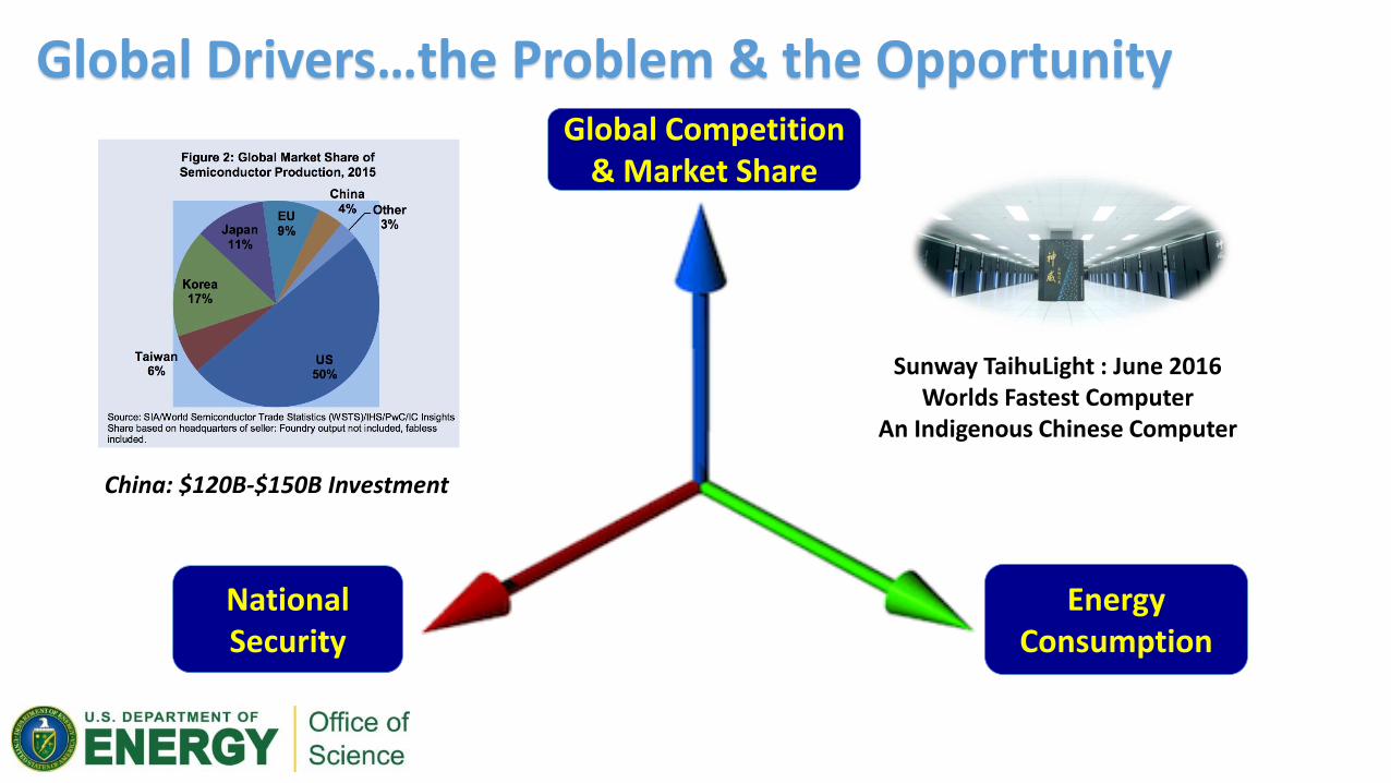
Global Drivers…the Problem & the Opportunity Global Competition
& Market Share
Energy Consumption
National Security
Sunway TaihuLight : June 2016 Worlds Fastest Computer
An Indigenous Chinese Computer
China: $120B-$150B Investment

Uncertainty Threatens US Economic Growth • The world has changed – technology is changing
at a dramatic rate –Dennard Scaling has ended –End of Moore's Law looming
• The IT marketplace is also changing dramatically –PC sales have flattened –Handhelds dominate growth, H/W and S/W – Internet of Things (IoT): explosive growth –HPC vendor uncertainty
• Semiconductors were America’s number three manufactured export over the last five years –2014 sales were $172.9 billion –51 percent of the $335.8 billion global market
• Nine out of the top 20 semiconductor companies are American
• Worldwide OEM Electronics Assembly Market 2015 - Estimated at > $1.4 Trillion
Source: Intel
2015 - Q4 update Amounts in US$M Year on Year Growth in %
2014 2015 2016 2017 2014 2015 2016 2017
Americas 69,324 68,738 69,664 71,996 12.7 -0.8 1.3 3.3
Europe 37,459 34,258 33,698 34,536 7.4 -8.5 -1.6 2.5
Japan 34,830 31,102 31,277 32,125 0.1 -10.7 0.6 2.7
Asia Pacific 194,230 201,070 201,453 207,792 11.4 3.5 0.2 3.1
Total World - $M 335,843 335,168 336,092 346,450 9.9 -0.2 0.3 3.1
July 31, 2017 William Harrod 4
Worldwide semiconductor market Source WSTS: 02/25/2016
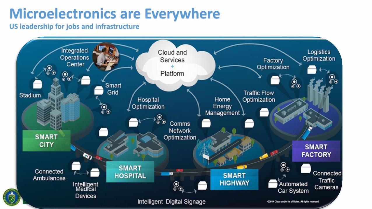
Microelectronics are Everywhere US leadership for jobs and infrastructure

Sunway TaihuLight System
6
• Developed by National Research Center of Parallel Computer Engineering & Technology
• Installed at National Supercomputing Center in Wuxi
• The system was funded from three sources, the central Chinese government, the province of Jiangsu, and the city of Wuxi for approximately $270M USD. That is the cost of the building, hardware, R&D, and software costs.
• The system, based on a homegrown processor and interconnect, demonstrates the significant progress that China has made in the domain of designing and manufacturing large-scale computation systems.
• It is capable of running real applications and is not just a “stunt machine”.
Specifcations: • ShenWei (Sunway) 26010 processor • Peak = 125.4PF (peak); 93PF LINPACK • 1.31 PB memory • 15MW power usage • Chilled water cooling • 5-level interconnection network • ~$270M for R&D + acquisition
http://www.netlib.org/utk/people/JackDongarra/PAPERS/sunway-report-2016.pdf

Technology Scaling Trends
Figure courtesy of Kunle Olukotun, Lance Hammond, Herb Sutter, and Burton Smith

From Giga to Exa, via Tera & Peta
1
10
100
1000
1986 1996 2006 2016
Rel
ativ
e Tr
ansi
sto
r Pe
rfo
rman
ce
Giga
Tera
Peta Exa
32x from transistor 32x from parallelism
8x from transistor 128x from parallelism
1.5x from transistor 670x from parallelism
Basic compute loop
Shekhar Borkar, Intel
July 31, 2017 William Harrod 8

There have been multiple recent assaults on “Moore’s Law”
Moore’s Law is an economic theory. There are ways to still scale digital technology after the end of
classical lithographic scaling
(e.g. end of Dennard Scaling in ~2004
No more exponential clock frequency scaling
Move to exponentially increasing parallelism)

Post-Lithographic Scaling Options There are other ways to continue Moore’s Scaling!
CMOSReconfigurableComputing
NewArchitecturesandPackaging
New
Device
san
dmaterials
y
x
3DStacking
TFETs
Spintronics
GeneralPurpose
CarbonNanotubesGraphene
DarkSilicon
PET
SystemonChip NTV
AttojouleSwitch
10 years scaling After 2025
20
ye
ars
scal
ing
w/1
0 y
ear
lea
d

John Shalf @ LBNL

Take the best ideas Rapidly evaluate for performance, integration,
and manufacturability
Develop and deploy
Materials • Low-D materials • Multiferroics • Non-linear optical
Devices • TFETs • Memristors • Optical logic
Architecture • Embedded memory • Optical interconnects • Non von Neumann • …
Everyone Industry
Chip Foundries • Intel • Global Foundries • TSMC Equipment Makers • AMAT • LAM • Lithography System • IBM • Dell • Google New startups • Multibeam e- • ALE
Materials
Devices
Architecture
Software
DOE National Labs
Advanced
Mfg
Executing the Multiscale CoDesign Framework

Fundamental science
Device physics
Device demonstration
System architecture
Programming paradigms
Multiscale CoDesign Framework
+++
+-
--
--
-
++
VTE
+
++
+
+
--
+
++
++
+
+
--
--
-
PtTaOxTa
On Chip Universal Memory:
Stacked ReRAM
Petabit cm-2
Densities
Replaces DRAM & flash
<1 pJ per write/read
Silicon
On Chip Memristor Accelerator:
Vector or matrix operations
fJs per operationOn Chip Photonics
Chip to chip communication
<1 pJ per bit transfer
High Performance Logic:
TFET, NcgFET
To next
node
x2
x2
x2
x2
w1,1
w2,1
w3,1
w4,1
w1,2
w2,2
w3,2
w4,2
w2,x
w2,x
w3,x
w4,x
...
...
...
...
Component integration
Mu
ltis
cale
C
oD
esi
gn
Fram
ewo
rk
Top
Do
wn
Bo
ttom
Up

The Opportunity… for DOE and the Nation Creating a Public-Private-Partnership
Fundamental Science (BES)
• From Lab to Fab • Accelerate development and
manufacturing base • Adv. manufacturing processes
• Multiscale computing benchmarking
• Heterogeneous architectures • New programming models
• Grand challenges driven research
• Scientific user facilities • Computational approaches to
materials design
Computing Science (ASCR, ASC)
Manufacturing Science (AMO, ARPAe)
Why DOE?
• Flagship HPC systems & applications • Unique scientific capabilities & tools • Multi-disciplinary expertise for co-design • History of collaborative Industry
engagements • Leadership under NSCI
Co-Design
Public – Private Partnerships
Co-Design
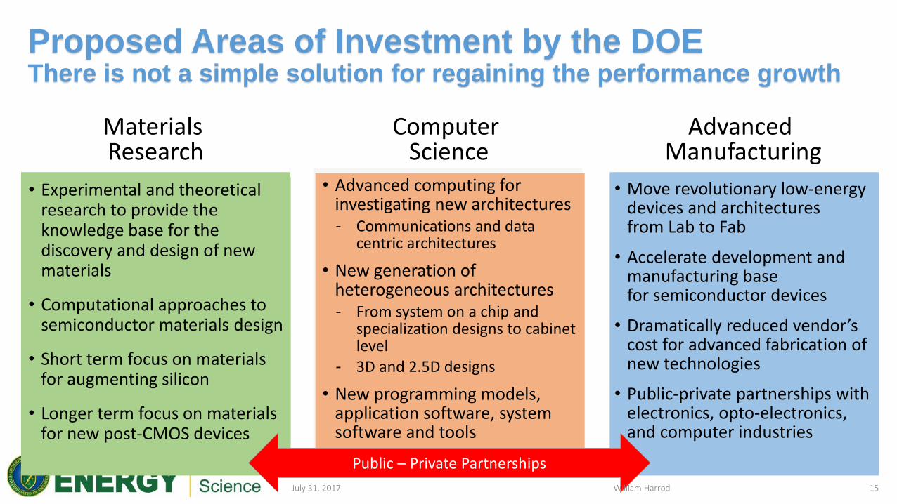
Advanced Manufacturing
Computer Science
Materials Research
• Move revolutionary low-energy devices and architectures from Lab to Fab
• Accelerate development and manufacturing base for semiconductor devices
• Dramatically reduced vendor’s cost for advanced fabrication of new technologies
• Public-private partnerships with electronics, opto-electronics, and computer industries
• Advanced computing for investigating new architectures - Communications and data
centric architectures
• New generation of heterogeneous architectures - From system on a chip and
specialization designs to cabinet level
- 3D and 2.5D designs
• New programming models, application software, system software and tools
• Experimental and theoretical research to provide the knowledge base for the discovery and design of new materials
• Computational approaches to semiconductor materials design
• Short term focus on materials for augmenting silicon
• Longer term focus on materials for new post-CMOS devices
Public – Private Partnerships
Proposed Areas of Investment by the DOE There is not a simple solution for regaining the performance growth
July 31, 2017 William Harrod 15

National Strategic Computing Initiative (NSCI) July 29, 2015
INTENT
• National - “Whole-of-government” / “whole-of-Nation” approach - Public/private partnership with industry and academia
• Strategic - Leverage beyond individual programs - Long time horizon (decade or more)
• Computing - HPC = most advanced, capable computing technology
available in a given era - Multiple styles of computing / all necessary
infrastructure - Scope: everything necessary for fully integrated
capability Theory and practice, software and hardware
• Initiative - Above baseline effort - Link and lift efforts
STRATEGIC THEMES
• Create systems that can apply exaflops of computing power to exabytes of data
• Keep the U.S. at the forefront of HPC capabilities
• Improve HPC application developer productivity
• Make HPC readily available
• Establish hardware technology for future HPC systems
July 31, 2017 William Harrod 16

NSCI Agencies
Department of Defense
Department of Energy
Department of Homeland Security
Federal Bureau of Investigation
Intelligence Advanced Research Projects Activity
National Aeronautics and Space Administration
National Institutes of Health
National Institute of Standards and Technology
National Oceanic and Atmospheric Administration
National Science Foundation
There are three lead agencies for NSCI: the Department of Energy (DOE), the Department of Defense (DOD), and the National Science Foundation (NSF).

Final Words
• The semiconductor industry is crucial to the U.S. economy – drives a > $2T/yr IT market
• What’s after CMOS? – augmented CMOS & substantially improved HW/SW architectures
• There is an exponentially increasing demand for information technology – new technologies are limited by cost to develop and manufacture, not due to a lack of innovations
• It isn’t clear what is the enabling technology for the “Post CMOS” | “Beyond Moore’s Law” epoch – requires involvement from many different organizations, demands innovations in architecture
• We need to stop trying to make tomorrow's computers look and operate like yesterday’s computers – don’t be constrained by the von Neumann paradigm
• We need to start investing in new materials, innovative architectural designs and the development of high performance, energy efficient, heterogeneous systems
• Need government-DOE laboratory-university-industry public-private partnership to attack the Beyond Moore’s Law challenges
July 31, 2017 William Harrod 18