engineering circuit analysis, 8th...
TRANSCRIPT
Engineering Circuit Analysis 8th Edition Chapter Six Exercise Solutions
Copyright ©2012 The McGraw-Hill Companies. Permission required for reproduction or display. All rights reserved.
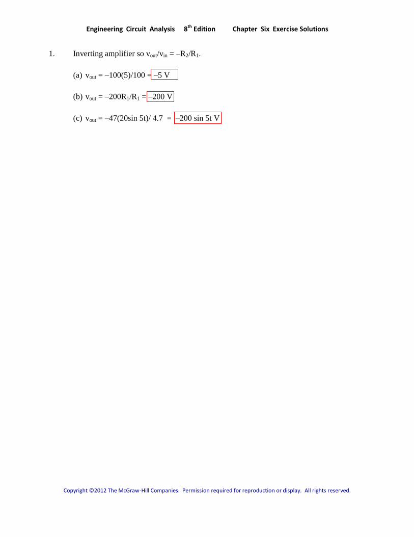
1. Inverting amplifier so vout/vin = –R2/R1.
(a) vout = –100(5)/100 = –5 V
(b) vout = –200R1/R1 = –200 V
(c) vout = –47(20sin 5t)/ 4.7 = –200 sin 5t V

Engineering Circuit Analysis 8th Edition Chapter Six Exercise Solutions
Copyright ©2012 The McGraw-Hill Companies. Permission required for reproduction or display. All rights reserved.
2. Inverting amplifier so vout/vin = –R2/R1.
P100 = (vout)2/100
R2/R1 vout (V) P100 (W)
(a) 0.5 –2 0.04
(b) 22 –88 77.44
(c) 101/100 –404/100 0.163

Engineering Circuit Analysis 8th Edition Chapter Six Exercise Solutions
Copyright ©2012 The McGraw-Hill Companies. Permission required for reproduction or display. All rights reserved.
3. Inverting op amp so vout = (1 + R2/R1)vin.
(a) vout = 10sin 10 t V
(b) vout = 30sin 10t V
(c) vout = 21(1.5 5 )te V
0 0.05 0.1 0.15 0.2 0.25 0.3 0.35 0.4 0.45 0.5-10
-8
-6
-4
-2
0
2
4
6
8
10
t (s)
va (
V)
0 0.05 0.1 0.15 0.2 0.25 0.3 0.35 0.4 0.45 0.5-30
-20
-10
0
10
20
30
t (s)
va (
V)
0 0.5 1 1.5 2 2.5 3 3.5 4 4.5 520
40
60
80
100
120
140
t (s)
va (
V)
Engineering Circuit Analysis 8th Edition Chapter Six Exercise Solutions
Copyright ©2012 The McGraw-Hill Companies. Permission required for reproduction or display. All rights reserved.
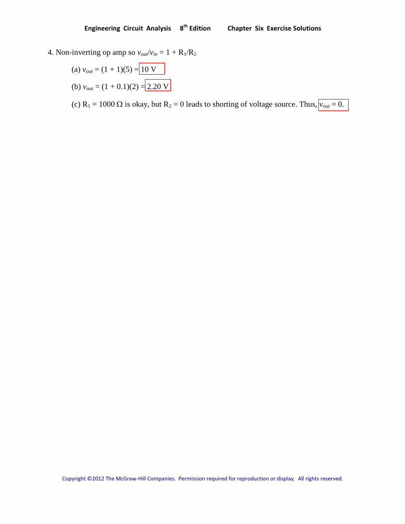
4. Non-inverting op amp so vout/vin = 1 + R1/R2
(a) vout = (1 + 1)(5) = 10 V
(b) vout = (1 + 0.1)(2) = 2.20 V
(c) R1 = 1000 is okay, but R2 = 0 leads to shorting of voltage source. Thus, vout = 0.
Engineering Circuit Analysis 8th Edition Chapter Six Exercise Solutions
Copyright ©2012 The McGraw-Hill Companies. Permission required for reproduction or display. All rights reserved.
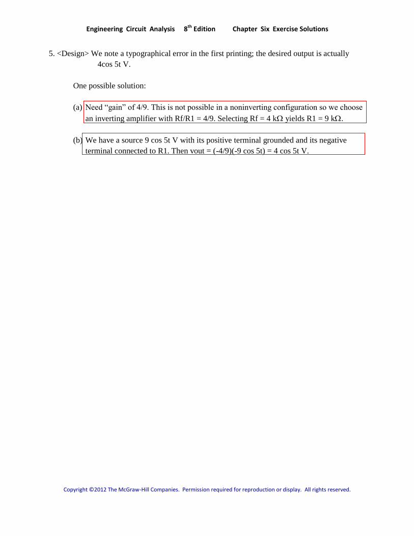
5. <Design> We note a typographical error in the first printing; the desired output is actually
4cos 5t V.
One possible solution:
(a) Need “gain” of 4/9. This is not possible in a noninverting configuration so we choose
an inverting amplifier with Rf/R1 = 4/9. Selecting Rf = 4 k yields R1 = 9 k.
(b) We have a source 9 cos 5t V with its positive terminal grounded and its negative
terminal connected to R1. Then vout = (-4/9)(-9 cos 5t) = 4 cos 5t V.

Engineering Circuit Analysis 8th Edition Chapter Six Exercise Solutions
Copyright ©2012 The McGraw-Hill Companies. Permission required for reproduction or display. All rights reserved.
6. <Design> One possible solution:
Since attenuation is required, only an inverting amplifier is appropriate. Thus, we need
Rf/R1 = 5/9. For standard 10% resistor values, selecting Rf = 10 leads to R1 = 18 .
Next, connect the negative terminal of a 9 V source to R1, and ground the positive
terminal of the source.

Engineering Circuit Analysis 8th Edition Chapter Six Exercise Solutions
Copyright ©2012 The McGraw-Hill Companies. Permission required for reproduction or display. All rights reserved.
7. The feedback resistor is R1, so vout = (1 + R1/R2)vin
We want (1 + 50/R2)2vin
2 = 250
(a) R2 = 23.12
(b) R2 = 5.241
Now we need (1 + 50/R2)2vin
2 = 110
(c) 45.55 ; 8.344
Engineering Circuit Analysis 8th Edition Chapter Six Exercise Solutions
Copyright ©2012 The McGraw-Hill Companies. Permission required for reproduction or display. All rights reserved.
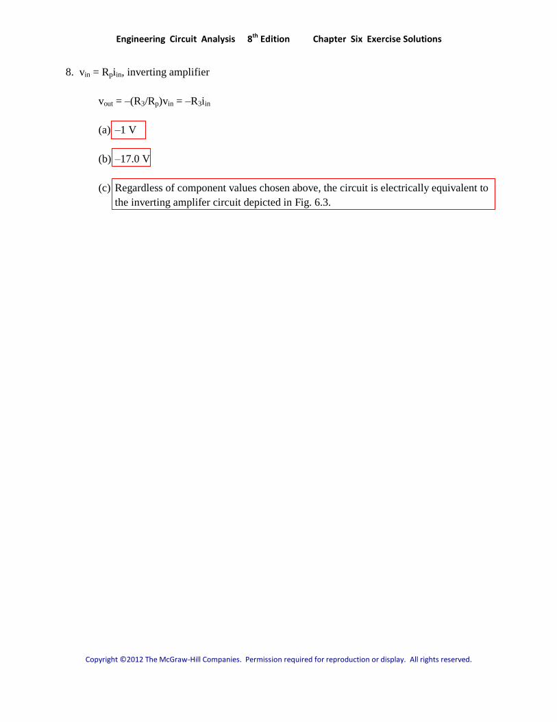
8. vin = Rpiin, inverting amplifier
vout = –(R3/Rp)vin = –R3iin
(a) –1 V
(b) –17.0 V
(c) Regardless of component values chosen above, the circuit is electrically equivalent to
the inverting amplifer circuit depicted in Fig. 6.3.
Engineering Circuit Analysis 8th Edition Chapter Six Exercise Solutions
Copyright ©2012 The McGraw-Hill Companies. Permission required for reproduction or display. All rights reserved.
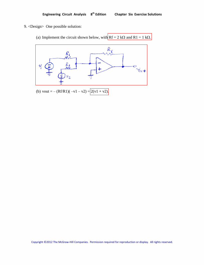
9. <Design> One possible solution:
(a) Implement the circuit shown below, with Rf = 2 k and R1 = 1 k.
(b) vout = – (Rf/R1)( –v1 – v2) = 2(v1 + v2).
Engineering Circuit Analysis 8th Edition Chapter Six Exercise Solutions
Copyright ©2012 The McGraw-Hill Companies. Permission required for reproduction or display. All rights reserved.
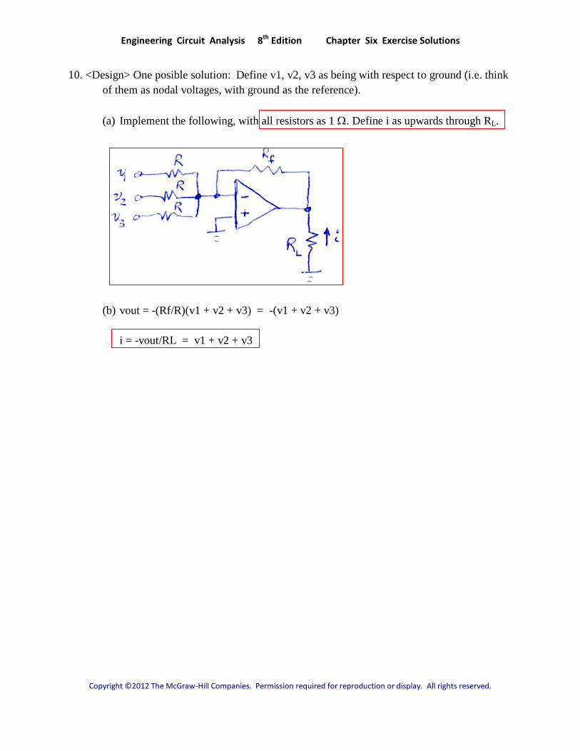
10. <Design> One posible solution: Define v1, v2, v3 as being with respect to ground (i.e. think
of them as nodal voltages, with ground as the reference).
(a) Implement the following, with all resistors as 1 . Define i as upwards through RL.
(b) vout = -(Rf/R)(v1 + v2 + v3) = -(v1 + v2 + v3)
i = -vout/RL = v1 + v2 + v3
Engineering Circuit Analysis 8th Edition Chapter Six Exercise Solutions
Copyright ©2012 The McGraw-Hill Companies. Permission required for reproduction or display. All rights reserved.
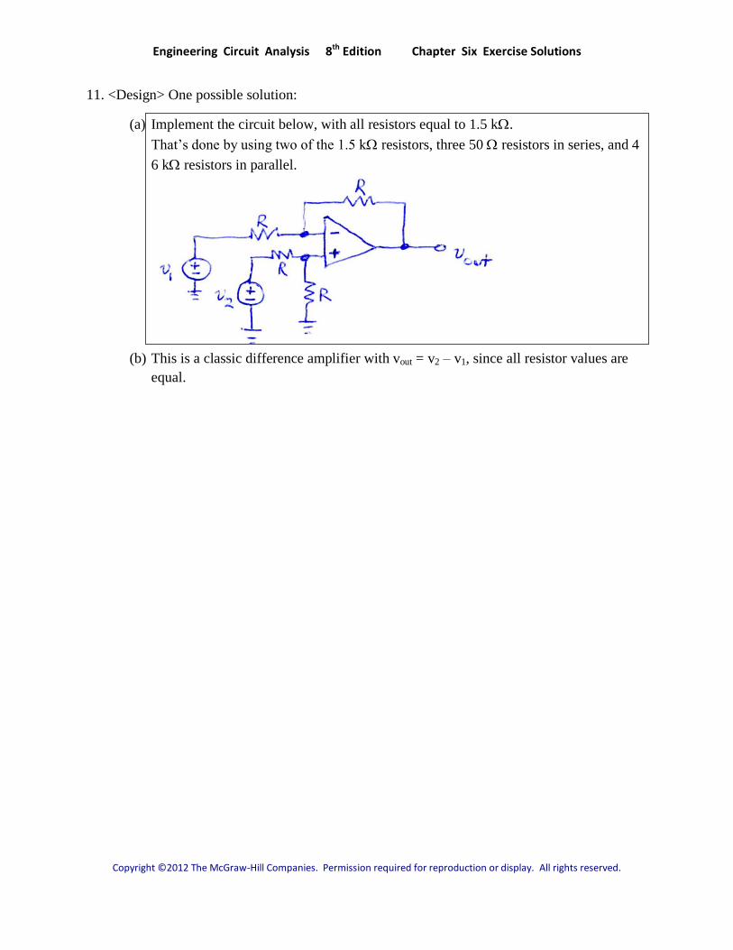
11. <Design> One possible solution:
(a) Implement the circuit below, with all resistors equal to 1.5 k.
That’s done by using two of the 1.5 k resistors, three 50 resistors in series, and 4
6 k resistors in parallel.
(b) This is a classic difference amplifier with vout = v2 – v1, since all resistor values are
equal.
Engineering Circuit Analysis 8th Edition Chapter Six Exercise Solutions
Copyright ©2012 The McGraw-Hill Companies. Permission required for reproduction or display. All rights reserved.
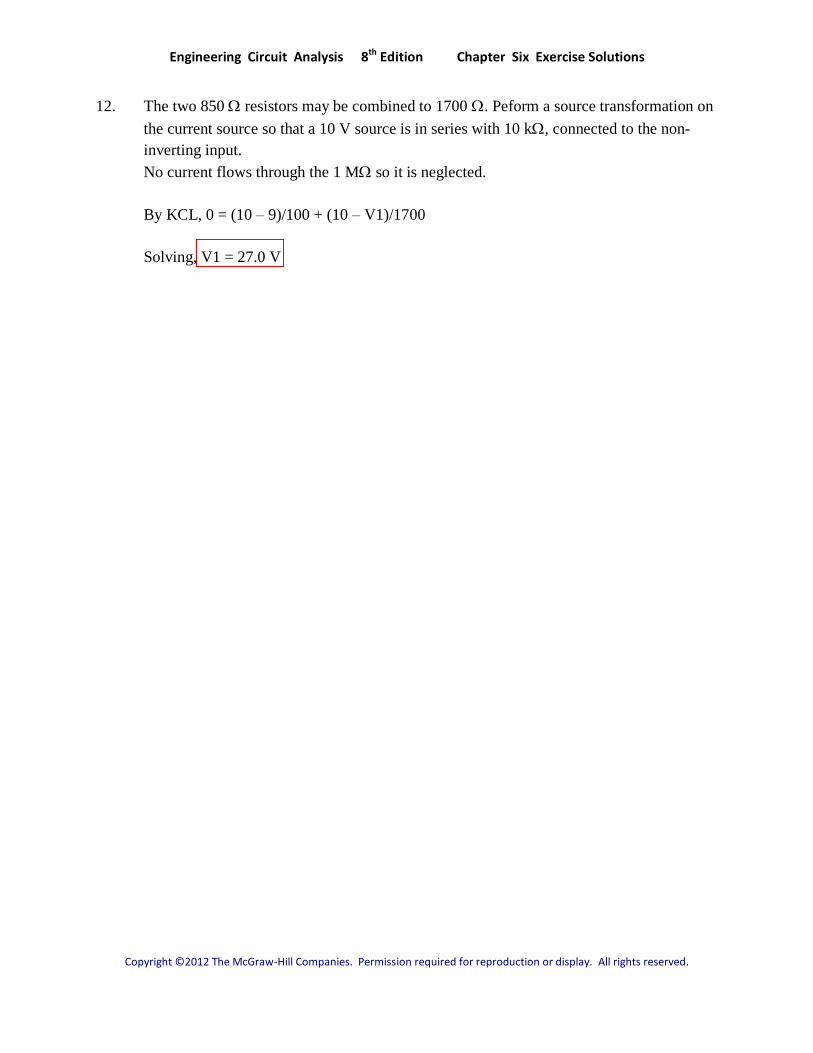
12. The two 850 resistors may be combined to 1700 . Peform a source transformation on
the current source so that a 10 V source is in series with 10 k, connected to the non-
inverting input.
No current flows through the 1 M so it is neglected.
By KCL, 0 = (10 – 9)/100 + (10 – V1)/1700
Solving, V1 = 27.0 V
Engineering Circuit Analysis 8th Edition Chapter Six Exercise Solutions
Copyright ©2012 The McGraw-Hill Companies. Permission required for reproduction or display. All rights reserved.
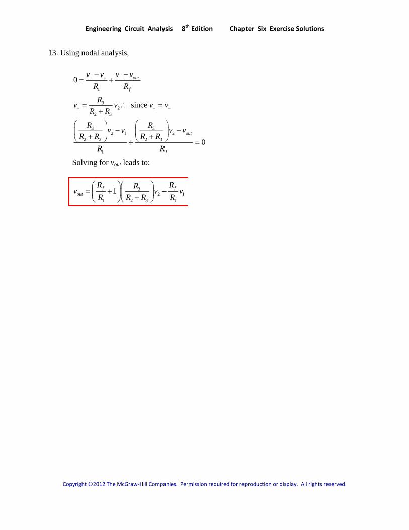
13. Using nodal analysis,
1
0 out
f
v vv v
R R
32
2 3
3 32 1 2
2 3 2 3
1
since
0
out
f
Rv v v v
R R
R Rv v v v
R R R R
R R
Solving for vout leads to:
32 1
1 2 3 1
1f f
out
R RRv v v
R R R R

Engineering Circuit Analysis 8th Edition Chapter Six Exercise Solutions
Copyright ©2012 The McGraw-Hill Companies. Permission required for reproduction or display. All rights reserved.
14. (a) No current can flow into either input pin of an ideal op amp.
(b) There can be no voltage difference between the input pins of an ideal op amp.
Engineering Circuit Analysis 8th Edition Chapter Six Exercise Solutions
Copyright ©2012 The McGraw-Hill Companies. Permission required for reproduction or display. All rights reserved.
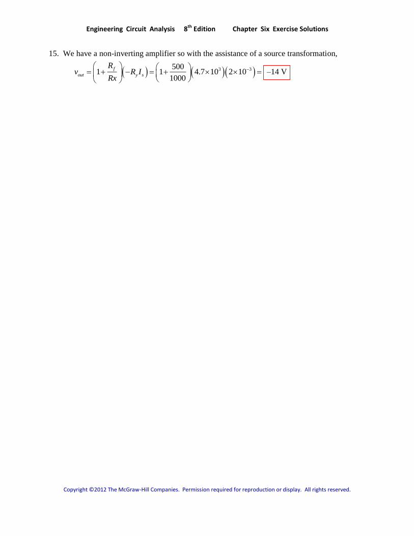
15. We have a non-inverting amplifier so with the assistance of a source transformation,
3 35001 1 4.7 10 2 10
1000
f
out y s
Rv R I
Rx
–14 V
Engineering Circuit Analysis 8th Edition Chapter Six Exercise Solutions
Copyright ©2012 The McGraw-Hill Companies. Permission required for reproduction or display. All rights reserved.
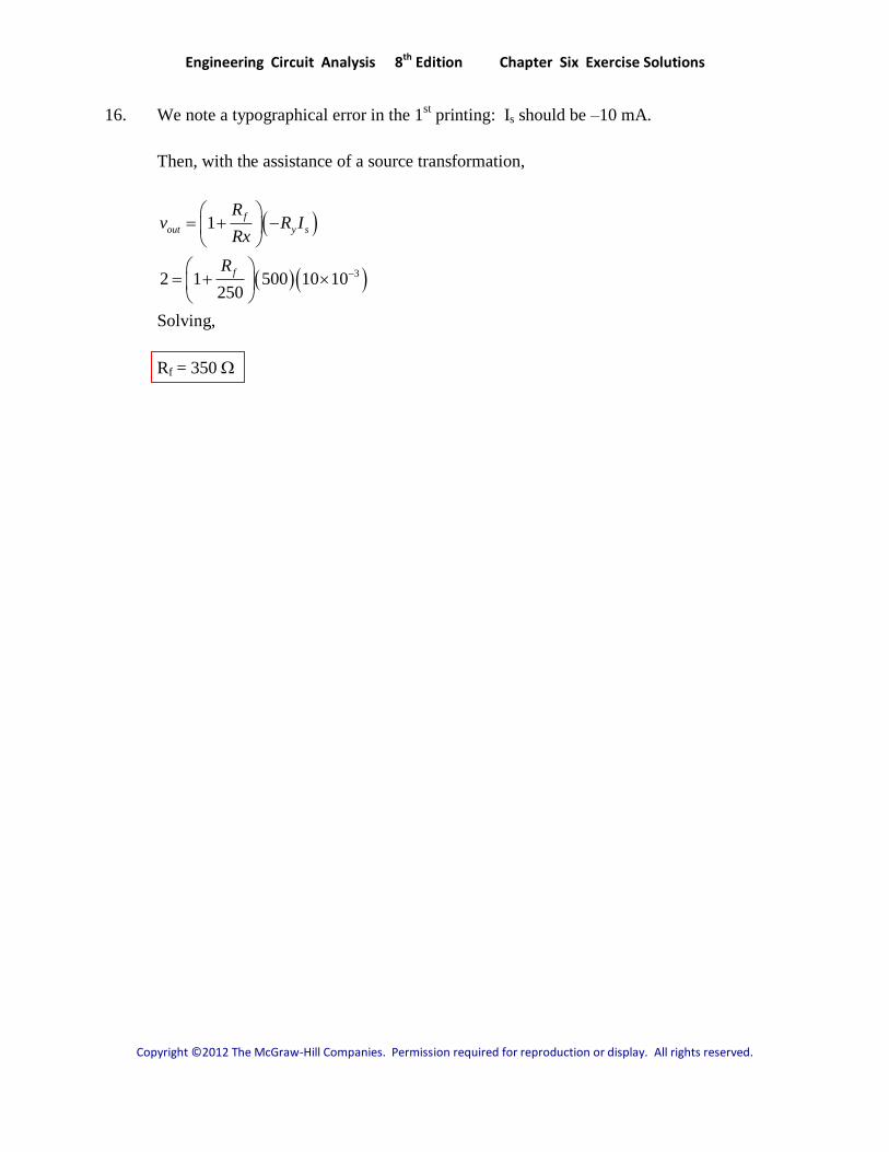
16. We note a typographical error in the 1st printing: Is should be –10 mA.
Then, with the assistance of a source transformation,
3
1
2 1 500 10 10250
f
out y s
f
Rv R I
Rx
R
Solving,
Rf = 350
Engineering Circuit Analysis 8th Edition Chapter Six Exercise Solutions
Copyright ©2012 The McGraw-Hill Companies. Permission required for reproduction or display. All rights reserved.
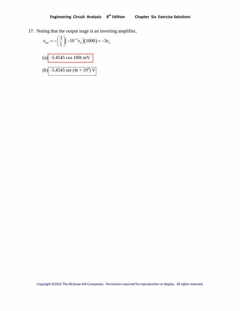
17. Noting that the output stage is an inverting amplifier,
3310 1000 3
1outv v v
(a) –5.4545 cos 100t mV
(b) –5.4545 sin (4t + 19o) V
Engineering Circuit Analysis 8th Edition Chapter Six Exercise Solutions
Copyright ©2012 The McGraw-Hill Companies. Permission required for reproduction or display. All rights reserved.
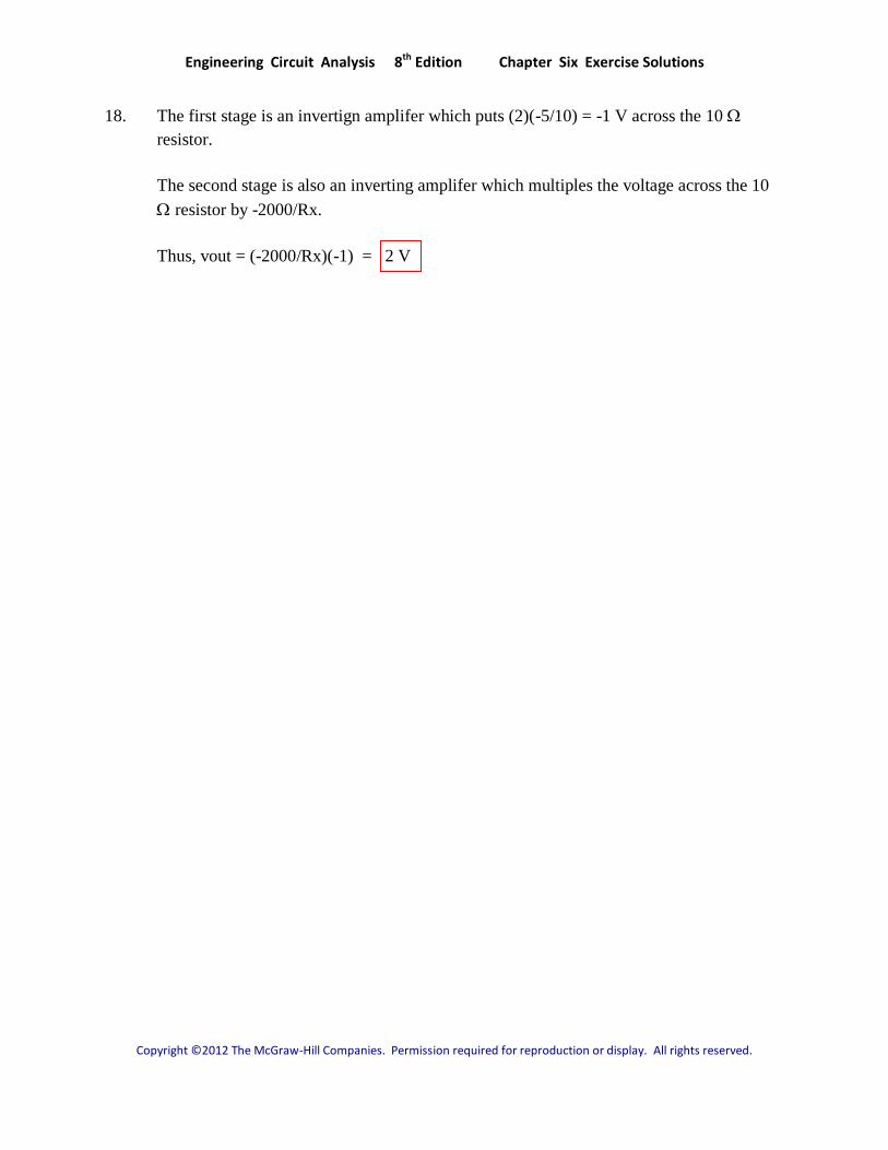
18. The first stage is an invertign amplifer which puts (2)(-5/10) = -1 V across the 10
resistor.
The second stage is also an inverting amplifer which multiples the voltage across the 10
resistor by -2000/Rx.
Thus, vout = (-2000/Rx)(-1) = 2 V

Engineering Circuit Analysis 8th Edition Chapter Six Exercise Solutions
Copyright ©2012 The McGraw-Hill Companies. Permission required for reproduction or display. All rights reserved.
19. Left stage is an inverting amplifer with gain -5/10 hence (-5/10)(2) = -1 V appears across
the 10 resistor.
The right hand stage is also an inverting amplifer, now with gain -2000/Rx (Rx in
ohms).
Thus, vout = (-1)(-2000/Rx) = 10 so Rx = 200
Engineering Circuit Analysis 8th Edition Chapter Six Exercise Solutions
Copyright ©2012 The McGraw-Hill Companies. Permission required for reproduction or display. All rights reserved.
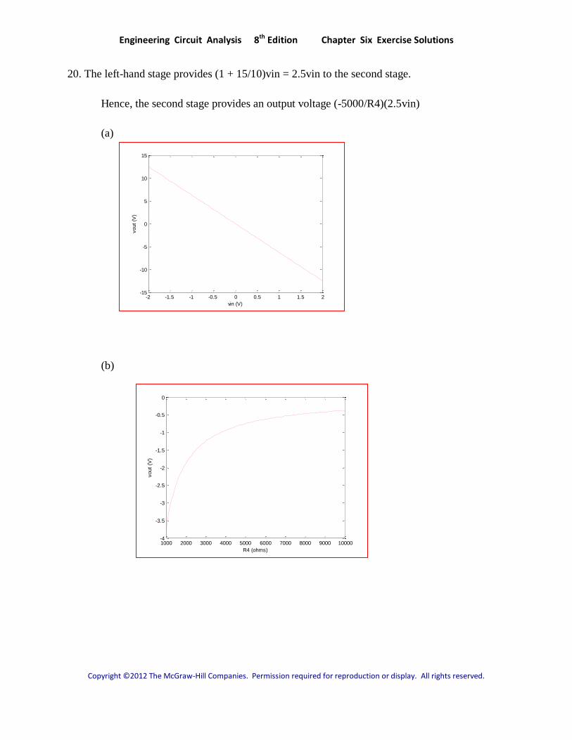
20. The left-hand stage provides (1 + 15/10)vin = 2.5vin to the second stage.
Hence, the second stage provides an output voltage (-5000/R4)(2.5vin)
(a)
(b)
-2 -1.5 -1 -0.5 0 0.5 1 1.5 2-15
-10
-5
0
5
10
15
vin (V)
vout
(V)
1000 2000 3000 4000 5000 6000 7000 8000 9000 10000-4
-3.5
-3
-2.5
-2
-1.5
-1
-0.5
0
R4 (ohms)
vout
(V)

Engineering Circuit Analysis 8th Edition Chapter Six Exercise Solutions
Copyright ©2012 The McGraw-Hill Companies. Permission required for reproduction or display. All rights reserved.
21. On the right we have a difference amplifer where vout = v1 – vleft
(vleft = output of left-hand stage).
So, vleft = (1.5)(-1500/500) = -4.5 V
Hence, vout =
(a) 0 – (-4.5) = 4.5 V
(b) 1 – (-4.5) = 5.5 V
(c) -5 – (-4.5) = -0.5 V
(d) 2sin100t + 4.5 V

Engineering Circuit Analysis 8th Edition Chapter Six Exercise Solutions
Copyright ©2012 The McGraw-Hill Companies. Permission required for reproduction or display. All rights reserved.
22. Stage 1 delivers vin(1 + 15/10) = 2.5vin to stage 2
Stage 2 delivers (-5000/2000)(2.5vin) = -6.25vin to stage 3
Stage 3 delivers (-1500/500)(-6.25vin) = 18.75vin to stage 4
Stage 4 delivers v1 – 18.75vin = vout
Thus,
(a) vout = 1 – 37.5 = -36.5 V
(b) vout = -18.75 V
(c) vout = -1 – 18.75 = -19.75 V

Engineering Circuit Analysis 8th Edition Chapter Six Exercise Solutions
Copyright ©2012 The McGraw-Hill Companies. Permission required for reproduction or display. All rights reserved.
23. The last stage is merely a buffer and has no effect on the output.
The remainder is a summing amplifier with (defining Rf = 200 k),
31 2
1 2 3
0 00 00 out
f
v vv v
R R R R
Solving, 33 31 2 1 2
1 2 3 1 2 3
200 10out f
v vv v v vv R
R R R R R R
(a) vout = -30.8 V
(b) vout = 0.8 V
Engineering Circuit Analysis 8th Edition Chapter Six Exercise Solutions
Copyright ©2012 The McGraw-Hill Companies. Permission required for reproduction or display. All rights reserved.
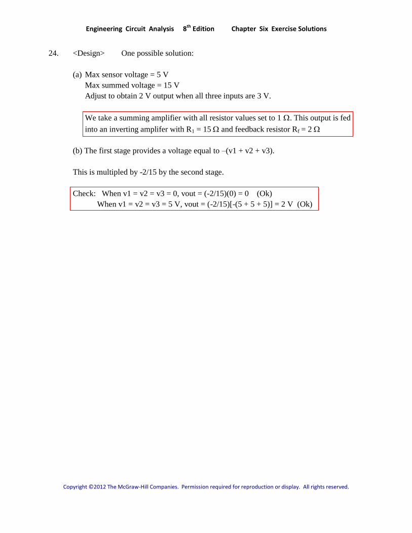
24. <Design> One possible solution:
(a) Max sensor voltage = 5 V
Max summed voltage = 15 V
Adjust to obtain 2 V output when all three inputs are 3 V.
We take a summing amplifier with all resistor values set to 1 . This output is fed
into an inverting amplifer with R1 = 15 and feedback resistor Rf = 2
(b) The first stage provides a voltage equal to –(v1 + v2 + v3).
This is multipled by -2/15 by the second stage.
Check: When v1 = v2 = v3 = 0, vout = (-2/15)(0) = 0 (Ok)
When v1 = v2 = v3 = 5 V, vout = (-2/15)[-(5 + 5 + 5)] = 2 V (Ok)
Engineering Circuit Analysis 8th Edition Chapter Six Exercise Solutions
Copyright ©2012 The McGraw-Hill Companies. Permission required for reproduction or display. All rights reserved.
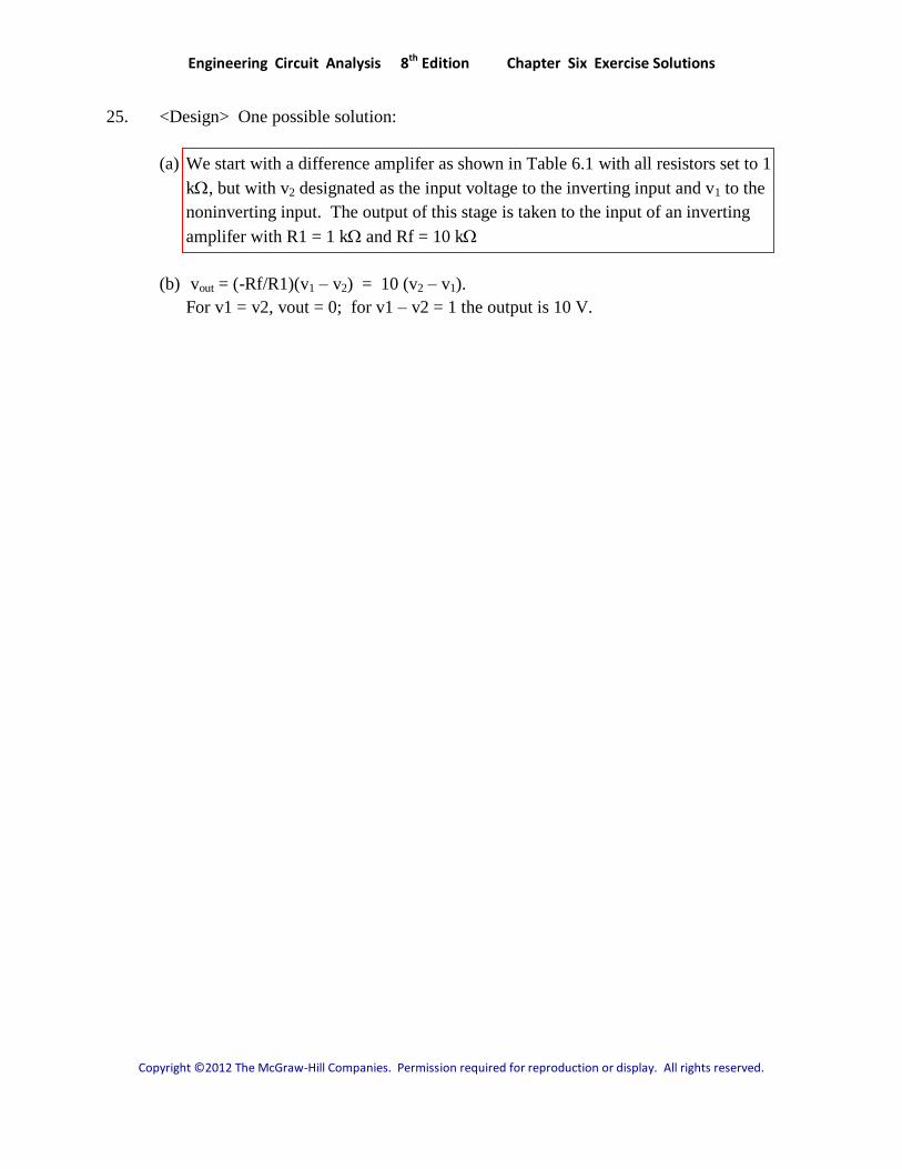
25. <Design> One possible solution:
(a) We start with a difference amplifer as shown in Table 6.1 with all resistors set to 1
k, but with v2 designated as the input voltage to the inverting input and v1 to the
noninverting input. The output of this stage is taken to the input of an inverting
amplifer with R1 = 1 k and Rf = 10 k
(b) vout = (-Rf/R1)(v1 – v2) = 10 (v2 – v1).
For v1 = v2, vout = 0; for v1 – v2 = 1 the output is 10 V.

Engineering Circuit Analysis 8th Edition Chapter Six Exercise Solutions
Copyright ©2012 The McGraw-Hill Companies. Permission required for reproduction or display. All rights reserved.
26. <Design> One possible solution:
(a) Maximum = 400,000 kg = 10 V
Sensor: 10 V = 1 kg therefore 400,000 kg on one sensor yields 4 V
We take a general summing amplifier with all resistors set to 1 k. The output of this
stage is taken as the input voltage to an inverting amplifier with R1 = 4 k and Rf = 10
k.
(b) The first stage sums the three sensor voltages v1, v2 and v3 to obtain –(v1 + v2 + v3)
at the input to the second stage. The second stage multiplies this voltage by -2.5.
If v1 + v2 + v3 = 4 V (400,000 kg total), vout = -2.5(-4) = 10 V.
Engineering Circuit Analysis 8th Edition Chapter Six Exercise Solutions
Copyright ©2012 The McGraw-Hill Companies. Permission required for reproduction or display. All rights reserved.
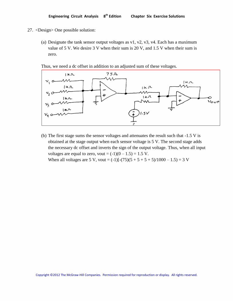
27. <Design> One possible solution:
(a) Designate the tank sensor output voltages as v1, v2, v3, v4. Each has a maximum
value of 5 V. We desire 3 V when their sum is 20 V, and 1.5 V when their sum is
zero.
Thus, we need a dc offset in addition to an adjusted sum of these voltages.
(b) The first stage sums the sensor voltages and attenuates the result such that -1.5 V is
obtained at the stage output when each sensor voltage is 5 V. The second stage adds
the necessary dc offset and inverts the sign of the output voltage. Thus, when all input
voltages are equal to zero, vout = (-1)(0 – 1.5) = 1.5 V.
When all voltages are 5 V, vout = (-1)[-(75)(5 + 5 + 5 + 5)/1000 – 1.5) = 3 V
Engineering Circuit Analysis 8th Edition Chapter Six Exercise Solutions
Copyright ©2012 The McGraw-Hill Companies. Permission required for reproduction or display. All rights reserved.
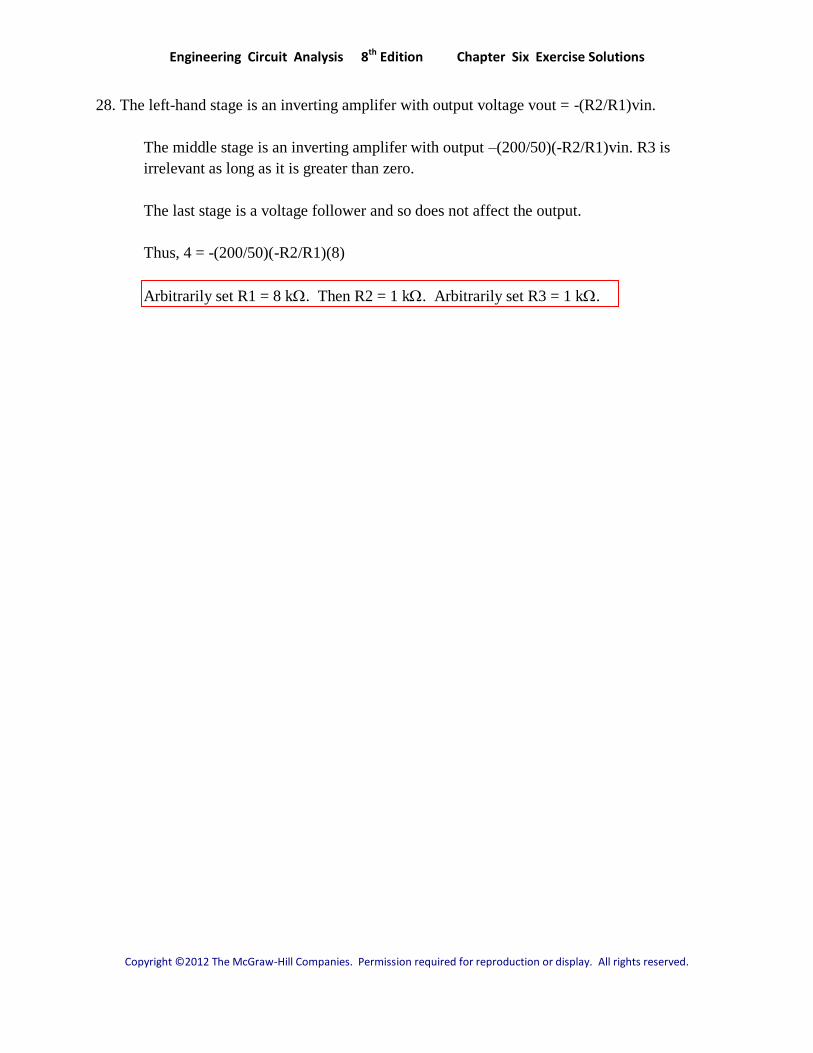
28. The left-hand stage is an inverting amplifer with output voltage vout = -(R2/R1)vin.
The middle stage is an inverting amplifer with output –(200/50)(-R2/R1)vin. R3 is
irrelevant as long as it is greater than zero.
The last stage is a voltage follower and so does not affect the output.
Thus, 4 = -(200/50)(-R2/R1)(8)
Arbitrarily set R1 = 8 k. Then R2 = 1 k. Arbitrarily set R3 = 1 k.

Engineering Circuit Analysis 8th Edition Chapter Six Exercise Solutions
Copyright ©2012 The McGraw-Hill Companies. Permission required for reproduction or display. All rights reserved.
29. The left-hand stage is a general difference amplifer. The right-hand stage is a simple
inverting amplifer which multiplies the output of the differnce amplifer by (1 + R6/R4).
Analyzing the left-hand stage then:
3
2 3
in
Rv v v
R R
So
4 1
10
out left hand stagev v v
R R
Substituting and solving for vout yields
34 6
4 1 2 3 1
1 1 1( )out in
Rv R R v
R R R R R

Engineering Circuit Analysis 8th Edition Chapter Six Exercise Solutions
Copyright ©2012 The McGraw-Hill Companies. Permission required for reproduction or display. All rights reserved.
30. <Design> One possible solution:
We use a circuit such as the one in Fig. 6.19a, but with two 9 V batteries in series for a
total of 18 V.
Then Rref = (18 – 10)/0.025 = 320

Engineering Circuit Analysis 8th Edition Chapter Six Exercise Solutions
Copyright ©2012 The McGraw-Hill Companies. Permission required for reproduction or display. All rights reserved.
31. <Design> One possible solution:
We can employ a voltage divider at the output as follows:
Then Rref = (9 – 5.1)/76×10-3
= 51.3
With 1 + Rf/R1 = 1, we set Rf= 0 and arbitrarily select R1 = 100
Finally,
1
(5.1) 1 4f L
L x
R R
R R R
With RL = 1 k, we find Rx = 275

Engineering Circuit Analysis 8th Edition Chapter Six Exercise Solutions
Copyright ©2012 The McGraw-Hill Companies. Permission required for reproduction or display. All rights reserved.
32. <Design> One possible solution:
(a) No diode is specified so we opt for the circuit of Fig. 6.20 and employ a 1N750,
which has a Zener voltage of 4.7 V. We base our design on the simulation result of
Fig. 6.19c, which shows a voltage of 4.733 V achieved at a current of 37.1 mA (Rref =
115 and 9 V source). Thus we need 1 + Rf/R1 = 5/4.8. For simplicity we select Rf
= 1 k so that R1 = 15.67 k.
(b) With an infinite load we are accurate to better than 1% of the target value (5 V).

Engineering Circuit Analysis 8th Edition Chapter Six Exercise Solutions
Copyright ©2012 The McGraw-Hill Companies. Permission required for reproduction or display. All rights reserved.
33. (a) A 1N750 Zener diode can be used to obtain a reference voltage of 4.7 V but the non-
inverting circuit of Fig. 6.20 cannot achieve a gain of less than unity. So, instead, employ
two cascaded inverting amplifiers, one to invert the sign of the voltage and one to reduce
the voltage from 4.7 V to 2.2 V. The circuit then is
With Vbat = 9 V, Rref = 115 , R1 = 1 k, Rf1 = 0, Rf2 = 1 k, and
Rf3 = (2.2/4.7)R1 = 468
(b) The evaluation version of PSpice will not allow the full circuit to be simulated, so we
omit the middle stage (used only to invert the sign) and simulate the rest, confirming
better than 1% accuracy with respect to our target value of 2.2 V.
Engineering Circuit Analysis 8th Edition Chapter Six Exercise Solutions
Copyright ©2012 The McGraw-Hill Companies. Permission required for reproduction or display. All rights reserved.
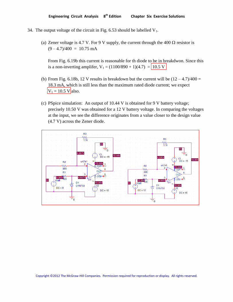
34. The output voltage of the circuit in Fig. 6.53 should be labelled V1.
(a) Zener voltage is 4.7 V. For 9 V supply, the current through the 400 resistor is
(9 – 4.7)/400 = 10.75 mA
From Fig. 6.19b this current is reasonable for th diode to be in breakdwon. Since this
is a non-inverting amplifer, V1 = (1100/890 + 1)(4.7) = 10.5 V
(b) From Fig. 6.18b, 12 V results in breakdown but the current will be (12 – 4.7)/400 =
18.3 mA, which is still less than the maximum rated diode current; we expect
V1 = 10.5 V also.
(c) PSpice simulation: An output of 10.44 V is obtained for 9 V battery voltage;
precisely 10.50 V was obtained for a 12 V battery voltage. In comparing the voltages
at the input, we see the difference originates from a value closer to the design value
(4.7 V) across the Zener diode.
Engineering Circuit Analysis 8th Edition Chapter Six Exercise Solutions
Copyright ©2012 The McGraw-Hill Companies. Permission required for reproduction or display. All rights reserved.
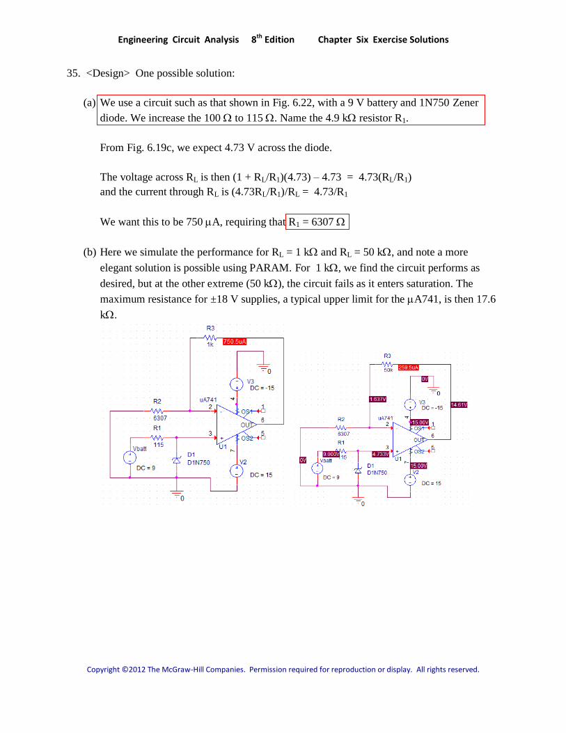
35. <Design> One possible solution:
(a) We use a circuit such as that shown in Fig. 6.22, with a 9 V battery and 1N750 Zener
diode. We increase the 100 to 115 . Name the 4.9 k resistor R1.
From Fig. 6.19c, we expect 4.73 V across the diode.
The voltage across RL is then (1 + RL/R1)(4.73) – 4.73 = 4.73(RL/R1)
and the current through RL is (4.73RL/R1)/RL = 4.73/R1
We want this to be 750 A, requiring that R1 = 6307
(b) Here we simulate the performance for RL = 1 k and RL = 50 k, and note a more
elegant solution is possible using PARAM. For 1 k, we find the circuit performs as
desired, but at the other extreme (50 k), the circuit fails as it enters saturation. The
maximum resistance for ±18 V supplies, a typical upper limit for the A741, is then 17.6
k.
Engineering Circuit Analysis 8th Edition Chapter Six Exercise Solutions
Copyright ©2012 The McGraw-Hill Companies. Permission required for reproduction or display. All rights reserved.
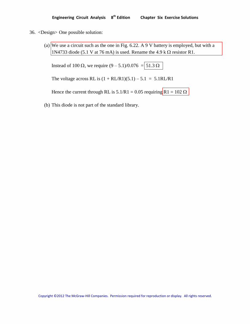
36. <Design> One possible solution:
(a) We use a circuit such as the one in Fig. 6.22. A 9 V battery is employed, but with a
1N4733 diode (5.1 V at 76 mA) is used. Rename the 4.9 k resistor R1.
Instead of 100 , we require (9 – 5.1)/0.076 = 51.3
The voltage across RL is (1 + RL/R1)(5.1) – 5.1 = 5.1RL/R1
Hence the current through RL is 5.1/R1 = 0.05 requiring R1 = 102
(b) This diode is not part of the standard library.

Engineering Circuit Analysis 8th Edition Chapter Six Exercise Solutions
Copyright ©2012 The McGraw-Hill Companies. Permission required for reproduction or display. All rights reserved.
37. (a) We design a circuit based on that shown in Fig. 6.22 but using the specified diode
instead. With a battery voltage of 24 V, assuming 20 V across the Zener diode and a
diode current of 50% its maximum (12.5 mA), we compute
Rref = (24 – 20)/0.00625 = 640
Then, since Is = Vref/R1, we require R1 = 20/10×10-3
= 2 k
(b) This diode is not part of the standard library.

Engineering Circuit Analysis 8th Edition Chapter Six Exercise Solutions
Copyright ©2012 The McGraw-Hill Companies. Permission required for reproduction or display. All rights reserved.
38. Define nodeal voltages v- and v+ at the op amp input terminals. Then
2
1 2
0 outv vv v
R R
1
3 4
0 out
L
v vv v v
R R R
With an ideal op amp, v- = v+.
Solving, 1 4 2 4 1 2 3 4 2 3 2 4 2
1 3 4 1 4 2 3
( )L L L L
out
L L
R R R R R R v R R R R R R R R R vv
R R R R R R R R R
And 1 4 1 2 3 2
1 3 4 1 4 2 3
L
L L L
R R v R R vvI
R R R R R R R R R R

Engineering Circuit Analysis 8th Edition Chapter Six Exercise Solutions
Copyright ©2012 The McGraw-Hill Companies. Permission required for reproduction or display. All rights reserved.
39. Define two nodal voltages vm and vp at the inverting and non-inverting input terminals,
respectively. For an ideal op amp, vm = vp. Then,
01000 500
p p outv v v [1]
1
01000 100 500
p p p outv v v v v [2]
Solving, vp = v1/10 and IL = vp/100 = v1/1000 (independent of RL)
Engineering Circuit Analysis 8th Edition Chapter Six Exercise Solutions
Copyright ©2012 The McGraw-Hill Companies. Permission required for reproduction or display. All rights reserved.
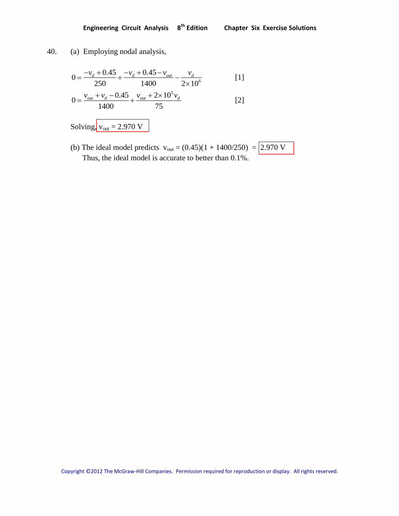
40. (a) Employing nodal analysis,
6
0.45 0.450
250 1400 2 10
d d out dv v v v
[1]
50.45 2 10
01400 75
out d out dv v v v [2]
Solving, vout = 2.970 V
(b) The ideal model predicts vout = (0.45)(1 + 1400/250) = 2.970 V
Thus, the ideal model is accurate to better than 0.1%.
Engineering Circuit Analysis 8th Edition Chapter Six Exercise Solutions
Copyright ©2012 The McGraw-Hill Companies. Permission required for reproduction or display. All rights reserved.
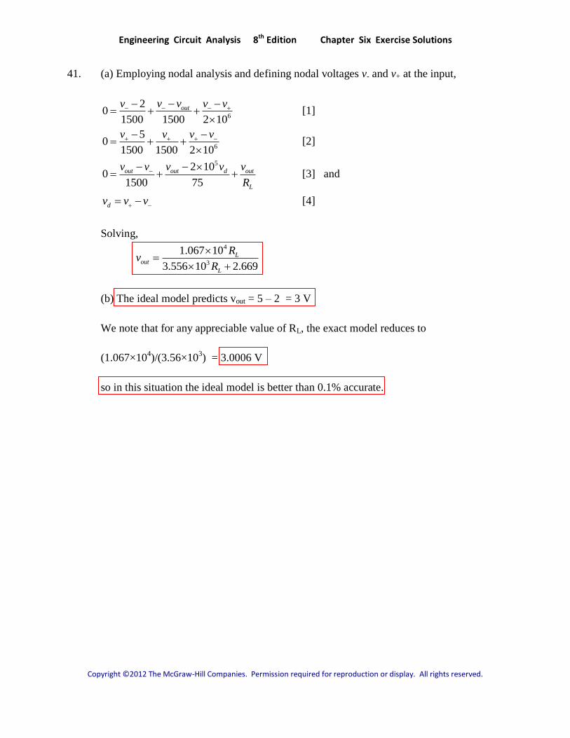
41. (a) Employing nodal analysis and defining nodal voltages v- and v+ at the input,
6
20
1500 1500 2 10
outv vv v v
[1]
6
50
1500 1500 2 10
v v v v
[2]
52 100
1500 75
out out d out
L
v v v v v
R
[3] and
dv v v [4]
Solving,
4
3
1.067 10
3.556 10 2.669
Lout
L
Rv
R
(b) The ideal model predicts vout = 5 – 2 = 3 V
We note that for any appreciable value of RL, the exact model reduces to
(1.067×10⁴)/(3.56×10
3) = 3.0006 V
so in this situation the ideal model is better than 0.1% accurate.

Engineering Circuit Analysis 8th Edition Chapter Six Exercise Solutions
Copyright ©2012 The McGraw-Hill Companies. Permission required for reproduction or display. All rights reserved.
42. (a) CMRR is the ratio of differential mode gain to common mode gain. If the same signal
is applied to both input terminals, ideally no output is generated. In reality, any
common component of the input voltages will be amplified slightly.
(b) Slew rate is the rate at which the output voltage can respond to changes in the input
voltage. This real limitation leads to distortion of the waveform above some
frequency.
(c) Saturation refers to the inability of an op amp circuit to generate an ouptutp voltage
larger than the supply voltage(s). If the input is too large, further increases do not lead
to correspondingly larger output.
(d) Feedback refers to routing some portion of the output to the input. Negative fedback
helps stabilize a circuit. Positive feedback can lead to oscillation.
Engineering Circuit Analysis 8th Edition Chapter Six Exercise Solutions
Copyright ©2012 The McGraw-Hill Companies. Permission required for reproduction or display. All rights reserved.
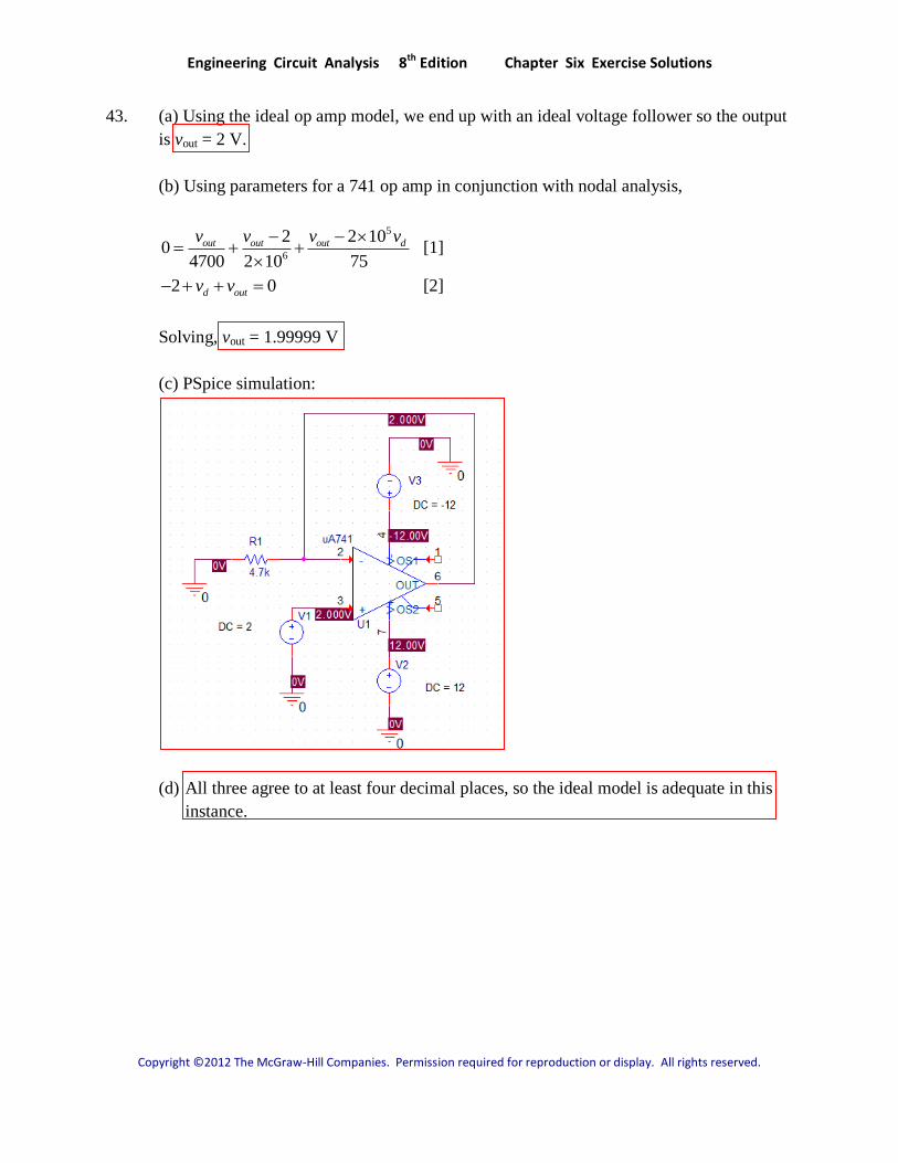
43. (a) Using the ideal op amp model, we end up with an ideal voltage follower so the output
is vout = 2 V.
(b) Using parameters for a 741 op amp in conjunction with nodal analysis,
5
6
2 2 100
4700 2 10 75
out out out dv v v v
[1]
2 0d outv v [2]
Solving, vout = 1.99999 V
(c) PSpice simulation:
(d) All three agree to at least four decimal places, so the ideal model is adequate in this
instance.
Engineering Circuit Analysis 8th Edition Chapter Six Exercise Solutions
Copyright ©2012 The McGraw-Hill Companies. Permission required for reproduction or display. All rights reserved.
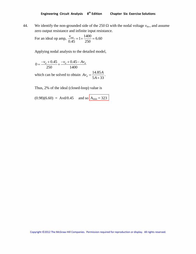
44. We identify the non-grounded side of the 250 with the nodal voltage vm., and assume
zero output resistance and infinite input resistance.
For an ideal op amp, 1400
1 6.600.45 250
outv
Applying nodal analysis to the detailed model,
0.45 0.45
0250 1400
d d dv v Av
which can be solved to obtain 14.85
5 33d
AAv
A
.
Thus, 2% of the ideal (closed-loop) value is
(0.98)(6.60) = Avd/0.45 and so Amin = 323
Engineering Circuit Analysis 8th Edition Chapter Six Exercise Solutions
Copyright ©2012 The McGraw-Hill Companies. Permission required for reproduction or display. All rights reserved.
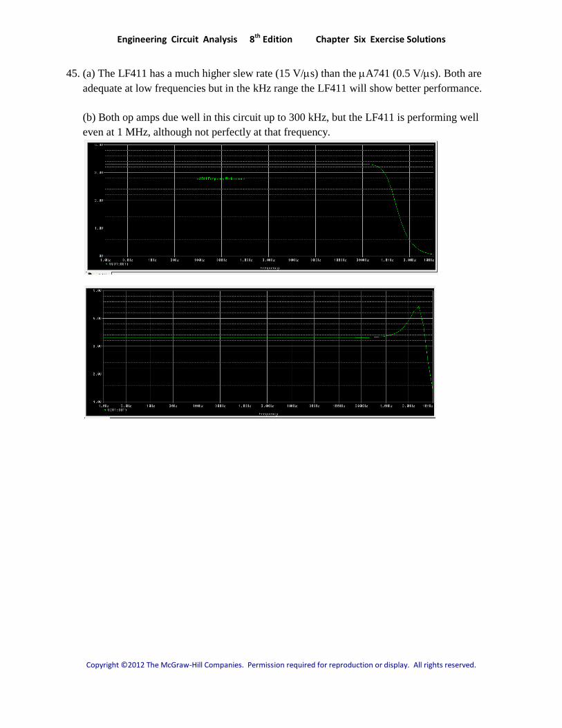
45. (a) The LF411 has a much higher slew rate (15 V/s) than the A741 (0.5 V/s). Both are
adequate at low frequencies but in the kHz range the LF411 will show better performance.
(b) Both op amps due well in this circuit up to 300 kHz, but the LF411 is performing well
even at 1 MHz, although not perfectly at that frequency.

Engineering Circuit Analysis 8th Edition Chapter Six Exercise Solutions
Copyright ©2012 The McGraw-Hill Companies. Permission required for reproduction or display. All rights reserved.
46. (a) This non-inverting amplifer has a gain of 1 + 470/4700 = 1.1
We therefore expect an output of (1.1)(2) = 2.2 V
The output voltage cannot exceed the supply voltage, or 9 V in this case.
Thus, (1 + Rf/4700)(2.2) = 9
Solving, Rfmax = 14.5 k
(b) Summary, using LF411: For Rf = 14.5 k, ideal model predicts 8.17 V, PSpice
yields 8.099 V, so we’re just barely in saturation with this value of resistance.
For Rf = 14 k, vout = 7.957 V as expected from the ideal model.
Engineering Circuit Analysis 8th Edition Chapter Six Exercise Solutions
Copyright ©2012 The McGraw-Hill Companies. Permission required for reproduction or display. All rights reserved.
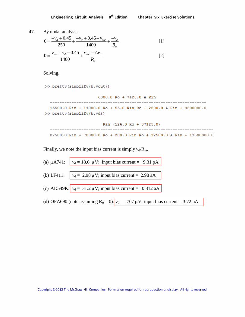
47. By nodal analysis,
0.45 0.45
0250 1400
d d out d
in
v v v v
R
[1]
0.45
01400
out d out d
o
v v v Av
R
[2]
Solving,
Finally, we note the input bias current is simply vd/Rin.
(a) A741: vd = 18.6 V; input bias current = 9.31 pA
(b) LF411: vd = 2.98 V; input bias current = 2.98 aA
(c) AD549K: vd = 31.2 V; input bias current = 0.312 aA
(d) OPA690 (note assuming Ro = 0): vd = 707 V; input bias current = 3.72 nA

Engineering Circuit Analysis 8th Edition Chapter Six Exercise Solutions
Copyright ©2012 The McGraw-Hill Companies. Permission required for reproduction or display. All rights reserved.
48. CMRRdb = 20logCM
A
A dB
where A = differential mode gain and ACM = common mode gain.
Solving, 2010
dBCM CMRR
AA
Device A CMRRdb ACM (V/V)
A741 2×10⁵ 90 6.3
LM324 105 85 5.6
LF411 2×10⁵ 100 2.0
AD549K 106 100 10.
OPA690 2800 65 1.6
Engineering Circuit Analysis 8th Edition Chapter Six Exercise Solutions
Copyright ©2012 The McGraw-Hill Companies. Permission required for reproduction or display. All rights reserved.
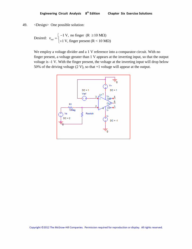
49. <Design> One possible solution:
Desired: 1 V, no finger (R 10 M )
1 V, finger present (R < 10 M )outv
We employ a voltage divider and a 1 V reference into a comparator circuit. With no
finger present, a voltage greater than 1 V appears at the inverting input, so that the output
voltage is -1 V. With the finger present, the voltage at the inverting input will drop below
50% of the driving voltage (2 V), so that +1 voltage will appear at the output.

Engineering Circuit Analysis 8th Edition Chapter Six Exercise Solutions
Copyright ©2012 The McGraw-Hill Companies. Permission required for reproduction or display. All rights reserved.
50. <Design> One possible solution:
We build a two-stage circuit where a comparator has vin applied to its non-inverting
input, and a 1 V reference to the inverting input. The output of this stage is 0 V when vin
> 1 V and -1.3 V otherwise. This is summed with a -1.2 V reference source, the output of
which is inverted and so is either +2.5 V for vin > 1 V or +1.2 V otherwise.
vin

Engineering Circuit Analysis 8th Edition Chapter Six Exercise Solutions
Copyright ©2012 The McGraw-Hill Companies. Permission required for reproduction or display. All rights reserved.
51. From Eq. [23],
4 2 1 2
3 4 3 1
1
1out
R R R Rv v v
R R R R
The differential input is v v and hence the differential gain is
4 2 1 2
3 4 3 1
1
1out
dm
R R R Rv v
R R R RvA
v v v v
[1]
For common mode components we must average the inputs, and hence the common-
mode gain is
4 2 1 2
3 4 3 1
1
12 2out
cm
R R R Rv v
R R R RvA
v v v v
[2]
CMRR is defined as the absolute value of their ratio: CMRR = dm
cm
A
A.
(a) 1 3 2 4 and R R R R . Eq. [1] above reduces to R2/R1.
Eq. [2] above reduces to 2
1
2cm
R v vA
R v v
. Thus, CMRR =
2
v v
v v
.
(b) All resistors are different. Then the above reduces to CMRR = 2
v v
v v

Engineering Circuit Analysis 8th Edition Chapter Six Exercise Solutions
Copyright ©2012 The McGraw-Hill Companies. Permission required for reproduction or display. All rights reserved.
53. Since the reference voltage v1 is applied to the inverting terminal, we expect the output to
follow the negative supply voltage (0 V, here) until vactive > vref at which point it follows
the positive voltage supply.
(a) Transition at vactive = -3 V
(b) Transition at vactive = +3 V
-5 -4 -3 -2 -1 0 1 2 3 4 50
2
4
6
8
10
12
14
16
18
vactive (V)
vout
(V)
-5 -4 -3 -2 -1 0 1 2 3 4 50
2
4
6
8
10
12
14
16
18
vactive (V)
vout
(V)
Engineering Circuit Analysis 8th Edition Chapter Six Exercise Solutions
Copyright ©2012 The McGraw-Hill Companies. Permission required for reproduction or display. All rights reserved.
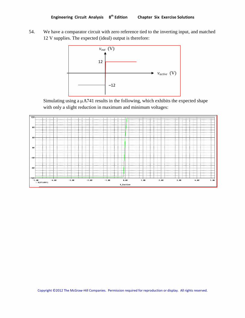
54. We have a comparator circuit with zero reference tied to the inverting input, and matched
12 V supplies. The expected (ideal) output is therefore:
Simulating using a A741 results in the following, which exhibits the expected shape
with only a slight reduction in maximum and minimum voltages:
vout (V)
vactive (V)
12
–12
Engineering Circuit Analysis 8th Edition Chapter Six Exercise Solutions
Copyright ©2012 The McGraw-Hill Companies. Permission required for reproduction or display. All rights reserved.
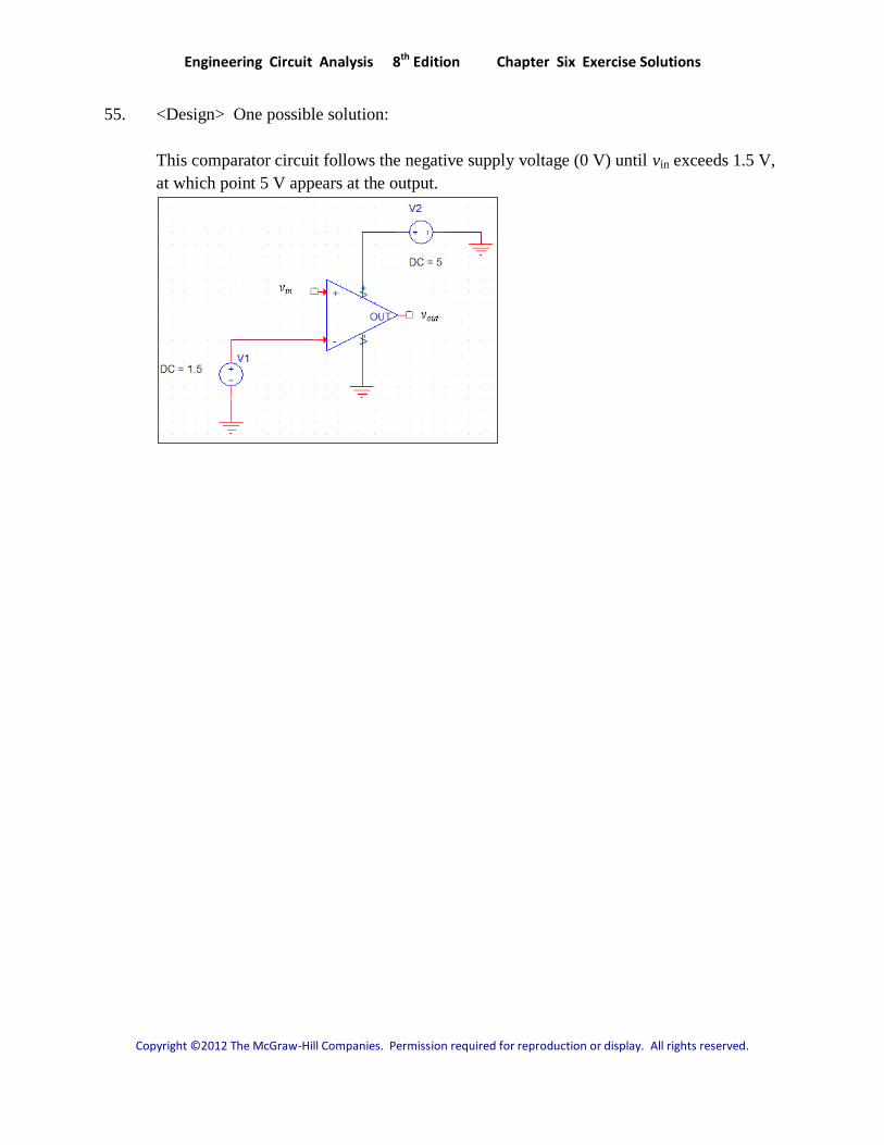
55. <Design> One possible solution:
This comparator circuit follows the negative supply voltage (0 V) until vin exceeds 1.5 V,
at which point 5 V appears at the output.
Engineering Circuit Analysis 8th Edition Chapter Six Exercise Solutions
Copyright ©2012 The McGraw-Hill Companies. Permission required for reproduction or display. All rights reserved.
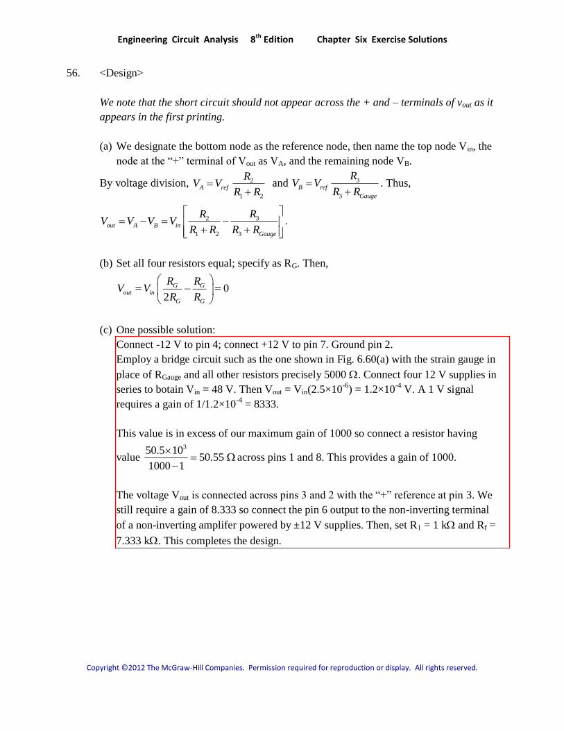
56. <Design>
We note that the short circuit should not appear across the + and – terminals of vout as it
appears in the first printing.
(a) We designate the bottom node as the reference node, then name the top node Vin, the
node at the “+” terminal of Vout as VA, and the remaining node VB.
By voltage division, 2
1 2
A ref
RV V
R R
and 3
3
B ref
Gauge
RV V
R R
. Thus,
32
1 2 3
out A B in
Gauge
RRV V V V
R R R R
.
(b) Set all four resistors equal; specify as RG. Then,
02
G Gout in
G G
R RV V
R R
(c) One possible solution:
Connect -12 V to pin 4; connect +12 V to pin 7. Ground pin 2.
Employ a bridge circuit such as the one shown in Fig. 6.60(a) with the strain gauge in
place of RGauge and all other resistors precisely 5000 . Connect four 12 V supplies in
series to botain Vin = 48 V. Then Vout = Vin(2.5×10⁻⁶
) = 1.2×10⁻⁴
V. A 1 V signal
requires a gain of 1/1.2×10-4
= 8333.
This value is in excess of our maximum gain of 1000 so connect a resistor having
value 350.5 10
50.55 1000 1
across pins 1 and 8. This provides a gain of 1000.
The voltage Vout is connected across pins 3 and 2 with the “+” reference at pin 3. We
still require a gain of 8.333 so connect the pin 6 output to the non-inverting terminal
of a non-inverting amplifer powered by ±12 V supplies. Then, set R1 = 1 k and Rf =
7.333 k. This completes the design.

Engineering Circuit Analysis 8th Edition Chapter Six Exercise Solutions
Copyright ©2012 The McGraw-Hill Companies. Permission required for reproduction or display. All rights reserved.
57. <Design> One possible solution:
(a) RTH of the switch = 5/1×10-3
= 5 k
We thus need a circuit with minimum gain 5/0.25 = 20
Select a non-inverting amplifer circuit. Connect the microphone to the non-inverting
input terminal, select R1 = 1 k and so Rf = 19 k.
(b) Although general speaking may not correspond to peak microphone voltage, we are
not provided sufficient information to address this, and not that he gain may need
adjusting in the final circuit.
Thus, we should connect the feedback resistor Rf in series with a variable 20 k
resistor, initially set to 0 . This will allow us to vary the actual gain between 1 +
Rf/R1 = 1 + 19/1 = 20 and 1 + 39/1 = 40.
Engineering Circuit Analysis 8th Edition Chapter Six Exercise Solutions
Copyright ©2012 The McGraw-Hill Companies. Permission required for reproduction or display. All rights reserved.
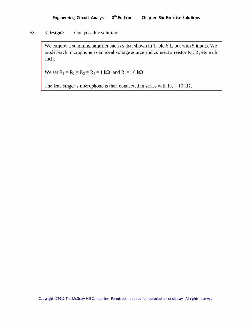
58. <Design> One possible solution:
We employ a summing amplifer such as that shown in Table 6.1, but with 5 inputs. We
model each microphone as an ideal voltage source and connect a reistor R1, R2 etc with
each.
We set R1 = R2 = R3 = R4 = 1 k and Rf = 10 k
The lead singer’s microphone is then connected in series with R5 = 10 k.

Engineering Circuit Analysis 8th Edition Chapter Six Exercise Solutions
Copyright ©2012 The McGraw-Hill Companies. Permission required for reproduction or display. All rights reserved.
59. <Design> One possible solution:
Rf(dark) = 100 k; Rf(light) = 10 k, measured at 6 candela.
Deliver 1.5 V to RL
Arbitrarily, select Vs = 1 V.
Assume the resistance scales linearly with light intensity, so
3 3
3100 10 10 102 candela (2) 100 10 70 k
0 6fR
With Rf = 70 k and vout = (1 + Rf/R1)Vs = 1.5, R1 = 2Rf = 140 k
Check:
0 candela leads to Rf = 100 k, so vout = (1 + 100/140)(1) = 1.7 V and it will not
activate.
6 candela leads to Rf = 10 k so vout = (1 + 10/140)(1) = 1.07 V and it will
activate.
Engineering Circuit Analysis 8th Edition Chapter Six Exercise Solutions
Copyright ©2012 The McGraw-Hill Companies. Permission required for reproduction or display. All rights reserved.
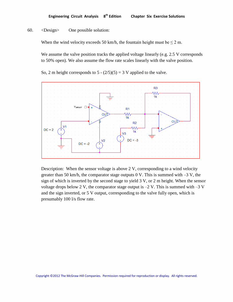
60. <Design> One possible solution:
When the wind velocity exceeds 50 km/h, the fountain height must be ≤ 2 m.
We assume the valve position tracks the applied voltage linearly (e.g. 2.5 V corresponds
to 50% open). We also assume the flow rate scales linearly with the valve position.
So, 2 m height corresponds to 5 - (2/5)(5) = 3 V applied to the valve.
Description: When the sensor voltage is above 2 V, corresponding to a wind velocity
greater than 50 km/h, the comparator stage outputs 0 V. This is summed with –3 V, the
sign of which is inverted by the second stage to yield 3 V, or 2 m height. When the sensor
voltage drops below 2 V, the comparator stage output is –2 V. This is summed with –3 V
and the sign inverted, or 5 V output, corresponding to the valve fully open, which is
presumably 100 l/s flow rate.

Engineering Circuit Analysis 8th Edition Chapter Six Exercise Solutions
Copyright ©2012 The McGraw-Hill Companies. Permission required for reproduction or display. All rights reserved.
61. By nodal analysis,
10 m m outv v v v
R R
[1]
22
2 2m
vRv v
R [2]
Consequently,
22 10.50.5
0 outv vv v
R R
and vout = v2 – v1. Thus, the resistor value is unimportant.
(a) (b)
(c)
0 0.1 0.2 0.3 0.4 0.5 0.6 0.7 0.8 0.9 1-8
-6
-4
-2
0
2
4
6
8
t (s)
vout
(V)
0 0.5 1 1.5 2 2.5 3 3.5 4 4.5 5-2
-1.9
-1.8
-1.7
-1.6
-1.5
-1.4
-1.3
-1.2
-1.1
-1
t (s)
vout
(V)
0 0.5 1 1.5 2 2.5 3 3.5 4 4.5 5-0.8
-0.6
-0.4
-0.2
0
0.2
0.4
0.6
0.8
1
t (s)
vout
(V)