engineering electromagnetics-...
TRANSCRIPT
Department of Semiconductor Systems Engineering SoYoung Kim
Engineering Electromagnetics- 1 Lecture 15: Capacitance
SoYoung Kim
Department of Semiconductor Systems Engineering
College of Information and Communication Engineering
Sungkyunkwan University
Department of Semiconductor Systems Engineering SoYoung Kim
Outline
Midterm results
Capacitance - Applications
Calculating Capacitance
Capacitance and Resistance
Method of Images

Department of Semiconductor Systems Engineering SoYoung Kim
Capacitance Applications

Department of Semiconductor Systems Engineering SoYoung Kim
Why Capacitance?
Delay
RC delay determines the timing and clock speed of a layout
Noise
Coupling cap causes noise to adjacent signal lines

Department of Semiconductor Systems Engineering SoYoung Kim
Cap Extraction in VLSI Design Flow
Cap Extraction step generates RC network netlist file
STA tool calculates from the given RC network:
Interconnect delay
Path delay
Signal integrity
Cap extraction is a critical step for timing closure.

Department of Semiconductor Systems Engineering SoYoung Kim
Basic Theory
The famous equation:
Q = CV
The potential of a conductor(V) is proportional to the total charge(Q), i.e., the capacitance(C) is constant.
C depends on the geometry of conductors and on the permittivity of the medium between them.

Department of Semiconductor Systems Engineering SoYoung Kim
Analytic Cap Calculation

Department of Semiconductor Systems Engineering SoYoung Kim
Analytic Cap Calculation
Department of Semiconductor Systems Engineering SoYoung Kim
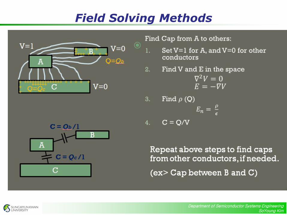
Field Solving Methods

Department of Semiconductor Systems Engineering SoYoung Kim
Field-Solving Method
Volume-Based Method Finite element method (FEM)…
Mesh is created in space surrounding conductors
Problem is represented by a large sparse matrix
Raphael 2D, Raphael 3D
Surface-Based Method Boundary element method (BEM)…
Mesh points are placed on surface of conductors, and boundary between different dielectric materials
Representing matrices are smaller than FEM’s, but dense.
Raphael BEM 2D, Raphael BEM 3D
Random-Walk Method Randomly pick points, starting from a conductor and ending
on other conductors (random walk)
No mesh needed – much more efficient than FEM or BEM
QuickCap, Rapid3d(ranxt)

Department of Semiconductor Systems Engineering SoYoung Kim
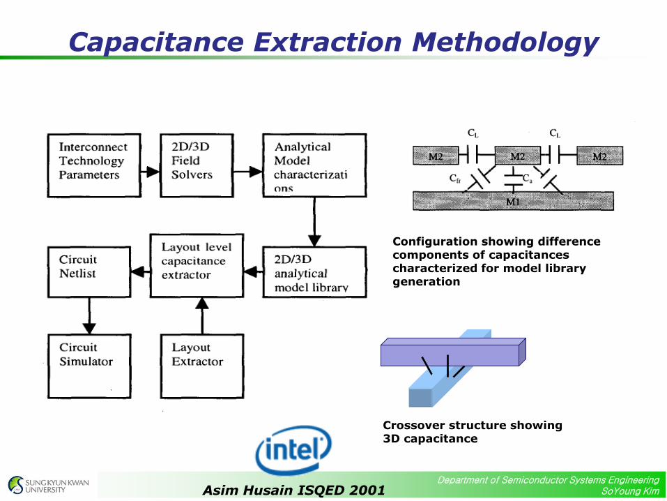
Capacitance Extraction Methodology
Field-Solver (FEM, BEM based)
Field-Solver (Randow walk based)
Department of Semiconductor Systems Engineering SoYoung Kim
Capacitance Extraction Methodology
Asim Husain ISQED 2001
Configuration showing difference components of capacitances characterized for model library generation
Crossover structure showing 3D capacitance
Department of Semiconductor Systems Engineering SoYoung Kim
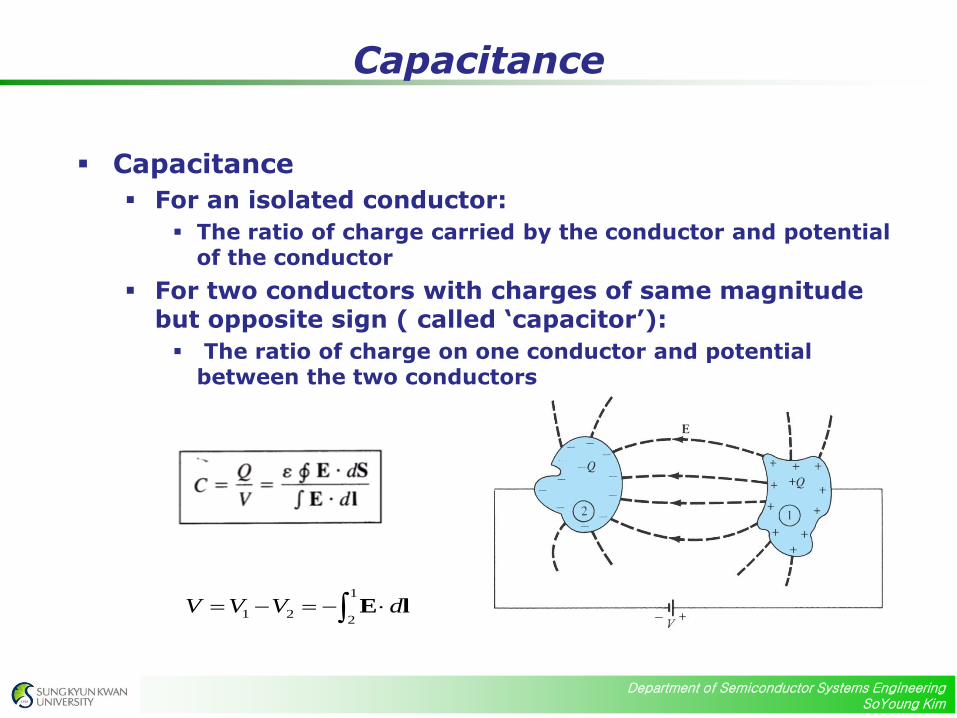
Capacitance
Capacitance
For an isolated conductor:
The ratio of charge carried by the conductor and potential of the conductor
For two conductors with charges of same magnitude but opposite sign ( called ‘capacitor’):
The ratio of charge on one conductor and potential between the two conductors
1
1 22
V V V d E l

Department of Semiconductor Systems Engineering SoYoung Kim
Procedures of Obtaining Capacitance
Methods of obtaining capacitance
Assuming Q and determining V in terms of Q (use Gauss’s law)
Assuming V and determining Q in terms of V (use Laplace’s equation)
Procedures for obtaining capacitance
Method #1
1. Choose a suitable coordinate system
2. Let the two conductors carry charges +Q and -Q
3. Determine E by Coulomb or Gauss’s law and find V.
4. Obtain C as Q/V
Method #2
1. Choose a suitable coordinate system
2. Let the two conductors have potential difference V0
3. Determine V by Laplace’s law, and find Q
4. Obtain C as Q/V

Department of Semiconductor Systems Engineering SoYoung Kim
Parallel-Plate Capacitor - Method #1
Potential between two plates
Capacitance
Energy stored in the capacitor
In general,
)
1
2 0
(
S
Sx x
d
x x
Q
S
Q
S
Q QdV d dx
S S
E a a
E l a a
Q SC
V d
2 2 2 2
2 2 2 2
1 1
2 2 2 2 2E
v
Q Q Sd Q d QW dv QV
S S S C
221 1
2 2 2E
QW CV QV
C
1
2E
vW dv D E

Department of Semiconductor Systems Engineering SoYoung Kim
– Laplace’s equation
– Boundary conditions
– Capacitance
Parallel-Plate Capacitor - Method #2
22
20
d VV
dx
V Ax B
0, 0 0 0
, 0o o
x V B
x d V V V Ad

Department of Semiconductor Systems Engineering SoYoung Kim
Coaxial Capacitor
Department of Semiconductor Systems Engineering SoYoung Kim
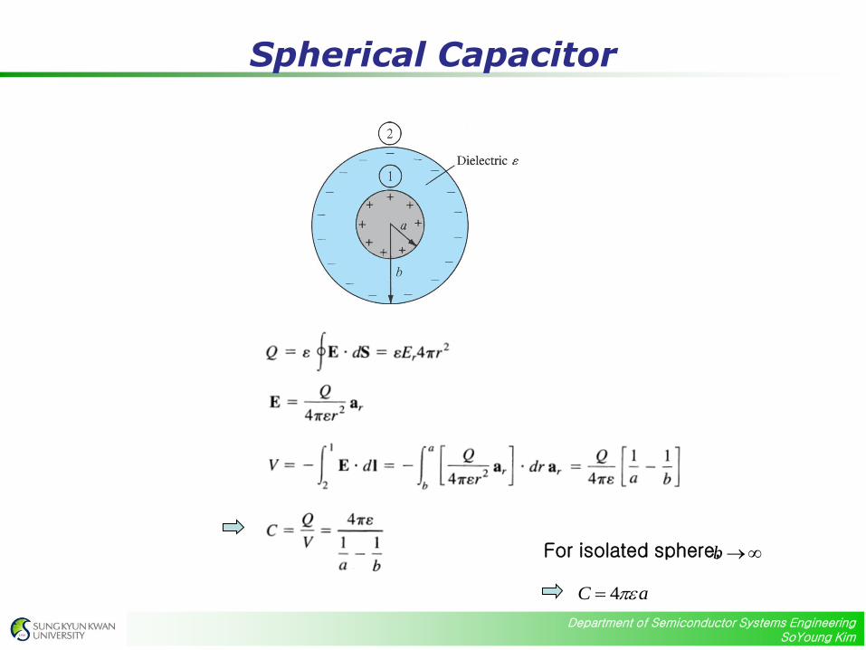
Spherical Capacitor
For isolated sphere, b
4C a

Department of Semiconductor Systems Engineering SoYoung Kim
– Laplace’s equation
– Boundary conditions
– Capacitance
Spherical Capacitor - Method #2
2 2
2
10
d dVV r
r dr dr
AV B
r
, 0 0 or
1 1, o o
A Ar b V B B
b b
r a V V V Ab a
22
22
0 02
1 1
1 1 1 1
4 4sin
1 11 1 1 1
oo r r r
o r o o r o
o
VdV Ar bV V V
dr rr
a b a b
V V QQ d r d d C
Vr
a ba b a b
E a a a
E S
Department of Semiconductor Systems Engineering SoYoung Kim
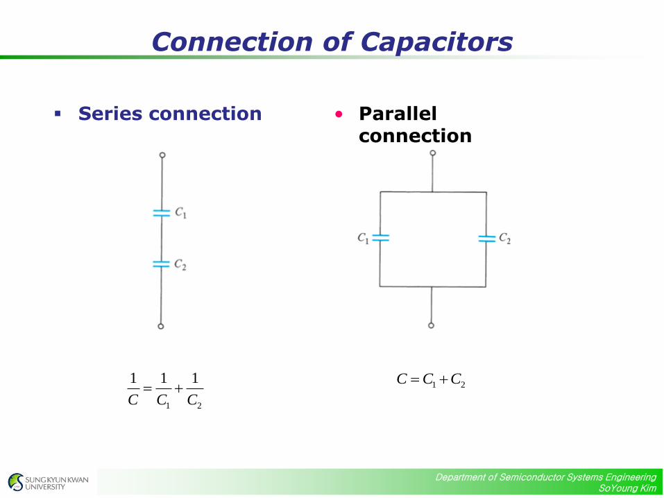
Connection of Capacitors
Series connection • Parallel connection
1 2
1 1 1
C C C 1 2C C C
Department of Semiconductor Systems Engineering SoYoung Kim
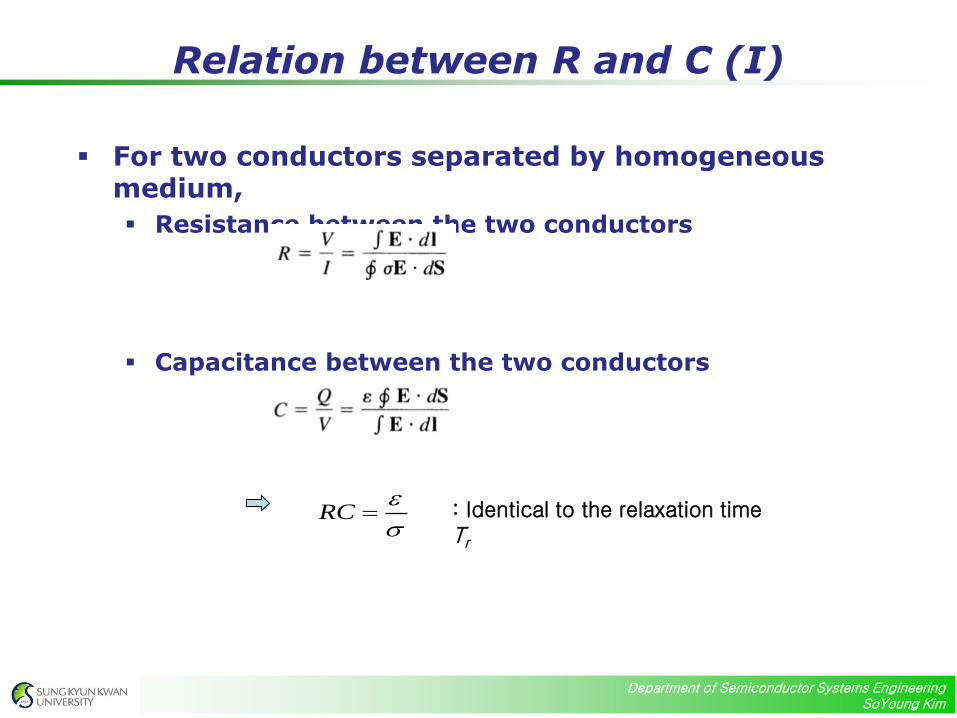
Relation between R and C (I)
For two conductors separated by homogeneous medium,
Resistance between the two conductors
Capacitance between the two conductors
: Identical to the relaxation time Tr
RC

Department of Semiconductor Systems Engineering SoYoung Kim
Relation between R and C (II)
Examples
Parallel capacitor
Cylindrical capacitor
Spherical capacitor
Isolated spherical capacitor
, S d
C Rd S
1n2 L
, 2
1n
b
aC Rb L
a
1 1
4,
1 1 4
a bC R
a b
14 ,
4C a R
a

Department of Semiconductor Systems Engineering SoYoung Kim
Method of Image
“A given charge configuration above an infinite grounded
perfect conducting plane may be replaced by the charge configuration itself, its image, and an equipotential surface in place of the conducting plane.”

Department of Semiconductor Systems Engineering SoYoung Kim
Method of Image
Two conditions need to be satisfied when method of image is used:
The image charge must be located in the conducting region
The potential on the conducting surface must be zero or constant

Department of Semiconductor Systems Engineering SoYoung Kim
Example 1
A point charge above a grounded conducting plane
Electric field
1 2
3 3
1 24 4o o
Q Q
r r
r rE E E
1
2
( , , ) (0,0, ) ( , , )
( , , ) (0,0, ) ( , , )
x y z h x y z h
x y z h x y z h
r
r
0z

Department of Semiconductor Systems Engineering SoYoung Kim
Example 1 (Cont’d)
Potential
Surface induced charge
1 2
1/2 1/22 2 2 2 2 2
4 4
1 1
4 ( ) ( )
o o
o
Q QV V V
r r
Q
x y z h x y z h
Department of Semiconductor Systems Engineering SoYoung Kim
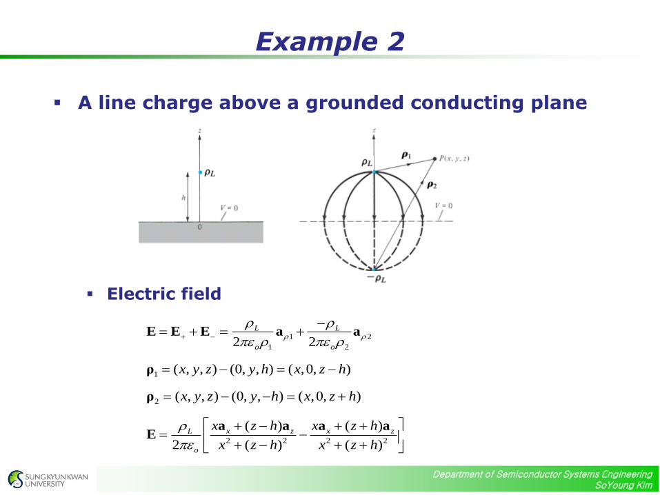
Example 2
A line charge above a grounded conducting plane
Electric field
1 2
1 2
1
2
2 2 2 2
2 2
( , , ) (0, , ) ( ,0, )
( , , ) (0, , ) ( ,0, )
( ) ( )
2 ( ) ( )
E E E a a
ρ
ρ
a a a aE
L L
o o
x z x zL
o
x y z y h x z h
x y z y h x z h
x z h x z h
x z h x z h

Department of Semiconductor Systems Engineering SoYoung Kim
Example 2 (Cont’d)
Potential
Surface induced charge
11 2
2
1/22 2
2 2
1n 1n 1n2 2 2
( ) or 1n
2 ( )
L L L
o o o
L
o
V V V
x z hV
x z h
0 2 2
2 2
LS n o z z
Li S
hD E
x h
h dxdx
x h
/2
/2
Li
L
h d
h
By letting tanx h

Department of Semiconductor Systems Engineering SoYoung Kim
Example 3
A point charge between two orthogonal semi-infinite conducting planes
Potential
29
1 2 3 4
1 1 1 1
4 o
QV
r r r r
1/22 2 2
1
1/22 2 2
2
1/22 2 2
3
1/22 2 2
4
( ) ( )
( ) ( )
( ) ( )
( ) ( )
r x a y z b
r x a y z b
r x a y z b
r x a y z b