enhanced near-field resolution in midinfrared using metamaterials
TRANSCRIPT

1Mcpaetlieetmmsspcotccdr
imtist�v(olssi
468 J. Opt. Soc. Am. B/Vol. 23, No. 3 /March 2006 Korobkin et al.
Enhanced near-field resolution in midinfraredusing metamaterials
Dmitriy Korobkin, Yaroslav Urzhumov, and Gennady Shvets
Department of Physics, The University of Texas at Austin, Austin, Texas 78712
Received July 21, 2005; accepted August 21, 2005
We demonstrate that a negative-permittivity material (silicon carbide) sandwiched between two layers ofpositive-permittivity material (silicon oxide) can be used for enhancement of the resolution of near-field imag-ing via the superlensing effect. The resulting three-layer metamaterial is also shown to exhibit an enhancedtransmission when its effective dielectric permittivity matches that of the vacuum. Experimental far-field di-agnostics of the superlensing based on measuring transmission coefficients through the metal-coated superlensis implemented using Fourier-transformed infrared microscopy. Superlensing is shown to be a highly resonantphenomenon manifested in a narrow frequency range. © 2006 Optical Society of America
OCIS codes: 310.6860, 240.6690.
mawpt
msbcqta�mettSoi
2RDooshpltlsf�=a
. INTRODUCTIONetamaterials is a general term referring to manmade
omposites of natural materials that have the desirableroperties unavailable in the naturally occurring materi-ls themselves. There has been a particular interest inngineering electromagnetic properties of metamaterialshat enable unconventional approaches to controllingight propagation. For example, metal-dielectric compos-tes have been used to enhance light intensity for nonlin-ar spectroscopic applications,1 enhance nonlinearffects,2 and design highly reflective3 or selectivelyransmissive4,5 mirrors. Even more exotic negative-indexaterials (NIMs)6–9 have been developed using theetamaterials approach, i.e., combining within the same
tructure various resonant elements10,11 that are respon-ible for the negative dielectric permittivity and magneticermeability of NIMs. One of the most fascinating appli-ations of NIMs is the so-called “superlens”12 capable ofvercoming the diffraction limit imposed by the wave na-ure of light on the smallest spot to which light can be fo-used. Although NIMs have been demonstrated in the mi-rowave part of the spectrum, they have not beenemonstrated in the highly desirable optical frequencyange, despite numerous13–15 theoretical suggestions.
The most fascinating metamaterials contain naturalngredients with both positive and negative dielectric per-
ittivity �. For example, a subwavelength diffraction pat-ern of a periodic slits array has been reproduced in themaging plane (on a photoresist) using a dielectric–silvertack.16,17 Enhanced transmission through a slab of nega-ive � material sandwiched between two layers of positivematerial has been recently demonstrated.5 Here we in-
estigate electromagnetic properties in the midinfraredmid-IR) frequency range of a metamaterial that consistsf a polar crystal (SiC) with ��0 sandwiched between twoayers of a conventional dielectric �SiO2� with �d�0. Thechematic of the metamaterial, with a point radiationource placed at the edge of SiO2, is shown in Fig. 1. Us-ng transmission–reflection measurements through the
0740-3224/06/030468-11/$15.00 © 2
etamaterial, we demonstrate that (a) transmission peaknd reflection drop are observed at the wavelength forhich the effective permittivity of the metamaterial ap-roaches unity and (b) that a � /9 spatial resolution is ob-ained using this metamaterial as a superlens.
This work breaks the new ground for developingetamaterials in the mid-IR part of the electromagnetic
pectrum that is of considerable interest for medicine andiology.18 Strong interest in mid-IR free-space communi-ations coupled with the recent breathtaking progress inuantum-cascade lasers19 provides yet another incentiveo the development of metamaterials in mid-IR. Anotherttraction of using polaritonic materials with the negativein mid-IR (e.g., SiC, ZnSe, TiO2) is that their electro-agnetic properties can be readily tuned by applying an
xternal electric field.20,21 We have used the Fourier-ransform-infrared (FTIR) microspectroscopy to charac-erize the dielectric permittivity of an ultrathin �400 nm�iC film grown heteroepitaxially22 on a Si wafer and dem-nstrated that it exhibits a negative dielectric permittiv-ty in mid-IR, with low losses.
. BACKGROUND: IMPROVING SPATIALESOLUTION WITH A SUPERLENSiffraction of light sets a natural limit on the resolutionf any conventional far-field imaging system. This limit isften referred to as the Abbe resolution limit of a micro-cope; features of an imaged object that are smaller thanalf wavelength of light � cannot be resolved in the imagelane. Another well-known example of the resolutionimit due to diffraction of light is a subwavelength diffrac-ion grating with a period D in the y direction. When il-uminated by a laser beam with the wavelength ��D,uch a diffraction grating produces only one (zeroth) dif-raction order in the far field. All other diffraction ordersm��1 are evanescent with the decay constants �v
m
2��m� /D. That implies that after a distance x�D /2�ll information about the diffraction grating is lost, and a
006 Optical Society of America

hputtitasadf
plwltwsttfioPefTn�i(
plnpwsfitltsttffi
lfcd�dbentroa
wFfibnkir
tttctpthsptfstvispma
3TsaxatlPBd
Fli�flsll
Korobkin et al. Vol. 23, No. 3 /March 2006/J. Opt. Soc. Am. B 469
ypothetical light-sensitive screen placed in the imagelane at a distance x behind the grating is going to beniformly illuminated. Mathematically, this blurring ofhe image is described by the spatial exponential decay ofhe transverse wavenumbers ky
�m�=2m� /D. Restoring thenformation about the grating (or, equivalently, makinghe intensity in the image plane nonuniform) requiresmplifying evanescent diffraction orders. It was recentlyuggested that such amplification can indeed beccomplished12 using metamaterials with the negative in-ex of refraction n=��, where ��0 and �0 are neededor n�0.
Unfortunately, NIMs in mid-IR have not yet been ex-erimentally demonstrated. Even more significantly,osses severely limit23–25 the thickness of a superlens. Itas recently demonstrated25 that, when realistic material
osses are accounted for, the resolution enhancement byhe superlens is limited to the near-field zone: d��,here d is the thickness of the superlens and � is the free-
pace wavelength of light. In the near-field zone the twoypes of waves, P polarized (with a magnetic field parallelo the NIM interface) and S polarized (with an electriceld parallel to the NIM interface) decouple from eachther. Electrostatics largely governs the behavior of the-polarized waves,12 and the value of becomes irrel-vant to excitation of the surface wave that is responsibleor the amplification of otherwise evanescent waves.herefore one does not need to employ NIMs for making aear-field superlens. Naturally occurring materials with�0 can be used instead. Low-loss negative � materialsnclude metals (mostly Ag and Au) and polar crystalsZnSe, GaP, SiC).26
The original proposal for a “perfect lens,”12 and the im-roved calculations27 advanced the idea of using a low-oss metal with ��−1 for significant improvement of theear-field resolution. We refer to the phenomenon of im-roving the near-field resolution by a slab of materialith ��0 as near-field superlensing. The significance of a
uperlens is that it improves spatial resolution of near-eld imaging. In other words, for a given distance be-ween the imaged object and the imaging plane, a super-ens creates a sharper (higher spatial resolution) imagehan that created without its assistance. Conversely, theuperlens enables the increasing of the distance betweenhe source and the imaging plane while maintaining spa-ial resolution. A realistic superlens does not “beat the dif-raction limit,” because such a limit exists only in the fareld.Resistive losses is not the only factor limiting the reso-
ution of a near-field superlens. Another importantactor27 is retardation, i.e., the finite thickness of the lensompared with the wavelength of light. Retardation effectominates over losses whenever the inequality � /�d�d�2d2 /c2 is satisfied,28 where ��−�d+ i� is the complex
ielectric permittivity of a negative � material surroundedy a regular dielectric with permittivity �d. Several recentxperiments16,17 used a relatively low-loss silver as aegative � material and were securely within the limits ofhis inequality. Therefore retardation was the dominantesolution-limiting factor. Theoretical calculations 27 dem-nstrate that, in the retardation-limited case, uniformmplification of a broad range of transverse wavenumbers
orks properly only for very thin superlenses, �d /c�0.3.or thicker superlenses there is still a significant ampli-cation coefficient T�ky� of the large transverse wavenum-ers ky in the image in comparison with the unassistedear-field image. However, T�ky� is not a flat function ofy. Therefore such a superlens can be used only for imag-ng objects of small transverse feature size that are sepa-ated from each other by a much larger distance.
Experimental results presented below demonstrate, forhe first time, submicrometer superlensing (or �� /9) athe mid-IR frequency. Thanks to our choice of the rela-ively long operating wavelength, we were able to fabri-ate an ultrathin SiO2–SiC–SiO2 superlens that satisfieshe small retardation condition.27 This demonstrationaves the way for various nanolithographic applicationshat can take advantage of the widely available andighly efficient CO2 laser. We have devised a spectro-copic far-field diagnostic of superlensing by producingeriodic arrays of submicrometer slits on both surfaces ofhe superlens, as shown in Fig. 5(a). One set of image-orming slits creates localized sources, whereas the otheret of diagnostic slits is used for collecting the transmit-ed light. Spatial localization of the image is confirmed byarying the lateral position of the diagnostic slits. By us-ng a broadly tunable FTIR microscope, we also demon-trated that near-field superlensing is a highly resonanthenomenon; it occurs for the frequency corresponding toatching dielectric permittivities of the polar material, �,
nd the surrounding dielectric substrate, �d: ��−�d.
. THEORY AND SIMULATIONShe principle of operation of a near-field superlens ishown in Fig. 1. A single subwavelength slit (or a periodicrray of slits spaced by D �) of width y � located at=0 is illuminated by a normally incident laser and is im-ged onto the focal plane behind the film. The focal dis-ance of a superlens is equal to the thickness of the po-aritonic material d. We assume that the imaging wave is
polarized, i. e., the nonvanishing field components arez, Ex, and Ey. Magnetic field Bz in the object plane can beecomposed into planar waves:
ig. 1. Schematic of a near-field superlens. A thin film of a po-aritonic material with a negative dielectric permittivity ��−�ds sandwiched between two layers of a regular dielectric with �d
0. The front side of the superlens is covered by a perfectly re-ecting metallic screen. A narrow (subwavelength) slit in acreen illuminated by a planar electromagnetic wave defines theight source. An image of the slit is formed on the back side of theens.
womi�
B=
T=
am−f�tm
wt�̄l�Bd
�as=mctptptdtud=ccu�
AEFfi=ittssisenmtmcFiE
Fpamtitjfa
470 J. Opt. Soc. Am. B/Vol. 23, No. 3 /March 2006 Korobkin et al.
Bz�x = 0,y� =�−�
+�
dkA�k�exp�iky�,
here A�k� is the wave amplitude. In the case of a peri-dic array of slits the integral turns into a sum of the har-onics of kD=2� /D: A�k�=�m=−�
+� Am��k−mkD�, where ms the diffractive order. It will be assumed that all �m�
1 diffractive orders are nonpropagating (evanescent).Given the magnetic-field distribution at the slit
z�y ,x=0�, the magnetic field in the image plane Bz�y ,x2d� is given by
Bz�y,x = 2d� =�−�
+�
dy�Bz�y�,x = 0�G�y − y��. �1�
he Green’s function G�y−y�� is given by23–25,28 G�2��−1−�
+�dkT�k�exp �iky�, where
T�k� =4��d/�d���p/��exp�− �dd�
��p/� + �d/�d�2 exp��pd� − ��p/� − �d/�d�2 exp�− �pd�,
�2�
nd the evanescence constants in the regular and polaraterials are, respectively, �d= �k2−�d�2 /c2� and �p= �k2
��2 /c2�. Perfect restoration of the image is possible onlyor �=−�d and �p=�d. For nonmagnetic materials �=1�p��d. Therefore T�k� cannot be equal to unity for all kerms. The expression for T�k� can be simplified in theost relevant limit of �k�� ��d�� /c and �=−�d+ i�:
T�k� �4exp�− 2kd�
��̄ − i�d�2/k2c2� + 4 exp�− 2kd�, �3�
here �̄=� /�d characterizes losses in the negative � ma-erial. If both positive and negative � materials are lossy,
is the sum of the losses in both materials. Note thatosses (proportional to �̄) and retardation (proportional tod�2 /k2c2) cumulatively cause T�k� to deviate from unity.ecause the highest resolved wavenumber k�1/d, retar-ation dominates when �̄ �d�2d2 /c2.As was earlier demonstrated,29 SiO2 and SiC have �d4 and �p�−4+0.25i at �=11 m. For an object to be im-
ged onto the focal plane, we have chosen a periodic set oflits of the width y=500 nm spaced by a period D2.5 m. Because the first evanescent diffraction maxi-um decays by one e-folding after a distance L=D /2�, a
onvincing demonstration of superlensing requires thathe lens’ thickness 2d�L. In the absence of near-field su-erlensing, an electromagnetic wave transmitted throughhe periodic array of slits in the object plane turns into alanar wave propagating normally to the lens after a dis-ance L behind the object plane. We ensure that this con-ition is satisfied by choosing the thickness of the SiC filmo be d=400 nm. Thus the focal plane is expected to beniformly illuminated if the laser frequency �=2�c /�oes not satisfy the superlensing condition Re�����−Re�d�. Nonuniform illumination can occur under twoonditions: (a) superlensing considered below and (b) ex-itation of the slab resonances30 of the slab superlens. Wese computer simulations to demonstrate superlensing at=11.0 m.
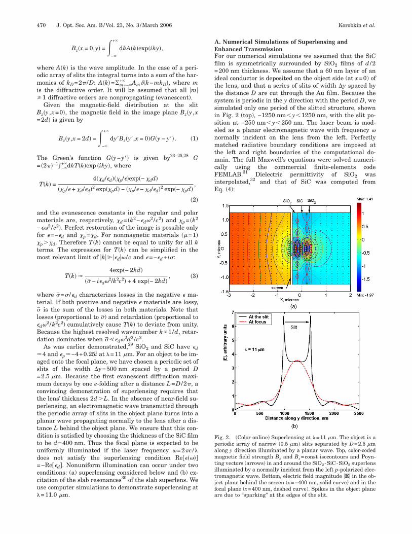
. Numerical Simulations of Superlensing andnhanced Transmissionor our numerical simulations we assumed that the SiClm is symmetrically surrounded by SiO2 films of d /2200 nm thickness. We assume that a 60 nm layer of an
deal conductor is deposited on the object side (at x=0) ofhe lens, and that a series of slits of width y spaced byhe distance D are cut through the Au film. Because theystem is periodic in the y direction with the period D, weimulated only one period of the slitted structure, shownn Fig. 2 (top), −1250 nm�y�1250 nm, with the slit po-ition at −250 nm�y�250 nm. The laser beam is mod-led as a planar electromagnetic wave with frequency �ormally incident on the lens from the left. Perfectlyatched radiative boundary conditions are imposed at
he left and right boundaries of the computational do-ain. The full Maxwell’s equations were solved numeri-
ally using the commercial finite-elements codeEMLAB.31 Dielectric permittivity of SiO2 was
nterpolated,32 and that of SiC was computed fromq. (4):
ig. 2. (Color online) Superlensing at �=11 m. The object is aeriodic array of narrow �0.5 m� slits separated by D=2.5 mlong y direction illuminated by a planar wave. Top, color-codedagnetic field strength Bz and Bz=const isocontours and Poyn-
ing vectors (arrows) in and around the SiO2-SiC-SiO2 superlenslluminated by a normally incident from the left p-polarized elec-romagnetic wave. Bottom, electric field magnitude �E� in the ob-ect plane behind the screen (x=−400 nm, solid curve) and in theocal plane (x=400 nm, dashed curve). Spikes in the object planere due to “sparking” at the edges of the slit.

w=iSttfi(imriproa
cestBf=srtapleitf
ticnePttlttpdt�sl
FSD=gamfi-S�
Fve0e+p�d
Korobkin et al. Vol. 23, No. 3 /March 2006/J. Opt. Soc. Am. B 471
� = ��
�2 − �LO2 + i��
�2 − �TO2 + i��
, �4�
here �LO=972 cm−1, �TO=796 cm−1, ��=6.5, and �5 cm−1.39 Superlensing at �=�0=11 m is demonstrated
n Fig. 2. Strong field enhancement at the right SiO2-iC boundary is indicative of evanescent wave amplifica-ion by the superlens. An image of the slit is formed onhe back side of the lens (SiO2–vacuum boundary). Pro-les of the electric-field amplitude behind the screensolid curve) and in the focal plane (curve line) are shownn Fig. 2 (bottom). While the sharp sparks behind the
etal screen are not resolved in the focal plane [they areepresented by a very large wavenumber k, such that T�k�s small], the overall width of the slit is captured. It is ap-arent from Fig. 2 (bottom) that the adjacent slits sepa-ated by D=2.5 m are well resolved. The actual FWHMf the slit image is better than D /2, which corresponds tospatial resolution better than � /8.Because superlensing is intimately related to amplifi-
ation of evanescent waves, we have studied the spatialvolution of the several harmonics of the imaged periodicet of slits inside the superlens. Magnetic field Bz insidehe superlens was decomposed into its spatial harmonics:z�x ,y�=�m=−�
+� Am�x�exp�imkDy�. The amplitudes of theour lowest spatial harmonics Am (A0, A−q+Aq, where q1,2,3) are plotted in Fig. 3. Clearly, the first and secondpatial harmonics are amplified by the SiC slab. The ze-oth harmonic responsible for the uniform illumination ofhe image plane is almost unchanged by SiC. The thirdnd higher harmonics are not amplified. This lack of am-lification for the higher harmonics sets the resolutionimit of our near-field superlens. To our knowledge, thisxperimental setup is the only superlens demonstrationn which a significant contribution of more than one spa-ial harmonic of a periodic object participates in the imageormation.
ig. 3. (Color online) Numerical simulation. Evolution of trans-erse Fourier harmonics along the optical axis x in a superlensxcited by a screen with a periodic array �D=2.5 m� of slits (.5 m wide), at the superlensing frequency ��=10.972 m�. Di-lectric constants used are �SiC=−3.76+0.24i and �SiO2
=3.760.17i. The first and second harmonics are dominated by the ex-onentially growing terms in the negative dielectric slab �−200x�200 nm�. The boundaries of the SiC and SiO2 layers are in-
icated by thick solid lines.
We have also simulated transmission of mid-IR radia-ion through the SiO2–SiC–SiO2 superlens without themage-forming metal screen. The purpose of this numeri-al experiment is to verify the recent prediction5 that aegative-� material can become totally transmissive whenncased inside a positive-� dielectric. Although Fabry–erot resonances of dielectric slabs, resulting in 100%
ransmission, are very well known, it is quite remarkablehat total transmission can be achieved with subwave-ength sandwich-like structures. The key to this effect ishat an electromagnetic wave propagating normally tohe material interface of a subwavelength structure andolarized parallel to the interface experiences an averageielectric permittivity given by the effective mediumheory33 (EMT): �����= �d1�1+d2�2� / �d1+d2�. Here d1,2 and1,2 label the thicknesses and dielectric permittivities, re-pectively, of the two materials comprising the subwave-ength sandwich. Total transmission through the struc-
ig. 4. (Color online) (a) Transmission through a three-layeriO2�200 nm�-SiC�400 nm�-SiO2�200 nm� nanostructure. Theot-dashed curve indicates perfect transparency at �1931 cm−1: simulation result; losses in SiO2 and SiC are ne-lected. The solid curve indicates the simulation result; lossesre included. The dashed curve indicates experimental measure-ents using a FTIR microscope. (b) Reflection from a 400 nm SiClm (dashed curve) and a SiO2�200 nm�-SiC�400 nm�SiO2�200 nm� composite film. Addition of the 400 nm (or � /25)iO2 coating reduces the reflection coefficient by a factor of 6 at=930 cm−1.

trlltnf
a=MdgtlTtatntbiccpctttc
BSsdtmFtd(sWwptmtiptt(ip(Fstct
itttiBtirSttTttocft�T
4Of
Foffloa
472 J. Opt. Soc. Am. B/Vol. 23, No. 3 /March 2006 Korobkin et al.
ure is expected if ��=1. This phenomenon cannot beealized for most materials: If �1,2�1, then �� �1. For po-ar materials with �2�0 there exists, however, a particu-ar frequency �1 for which ����1�=1. The physical basis forhe enhanced transmission is that the reflection from theegative-� material is exactly cancelled by the reflectionrom the positive-� coating.
Enhanced transmission was numerically simulated byssuming that �1��SiO2
,32 �2��SiC from Eq. (4), and d1d2=400 nm. The results of the numerical solution of theaxwell’s equations for the electromagnetic wave inci-
ent on the three-layer structure are shown in Fig. 4. Ne-lecting material losses in SiO2 and SiC by retaining onlyhe real part of the dielectric permittivity yields a dashed-ine curve indicating total transmission at �1=930 cm−1.his transmission maximum is expected to be experimen-ally observable because, at that frequency, losses in SiCnd SiO2 are small. The other two higher-frequencyransmission maxima are located close to phonon reso-ances of SiO2, where Re��SiO2
��0 and Re��SiC��0. Theseransmission maxima are not expected to be observable,ecause of the very high losses in SiO2. Indeed, when themaginary parts of the dielectric permittivities are in-luded, the transmission curve represented by the solidurve has a single well-formed maximum at �=�1. Theeak transmission falls short of 100% to about 92% be-ause of the finite losses. The experimentally measuredransmission curve (dashed curve) indeed closely trackshe numerically simulated solid curve. The small dip nearhe expected transmission maximum appears to beaused by sample contamination, resulting in absorption.
. Far-Field Diagnostic of Superlensingimulation results presented in Section 3.A indicate thatuperlensing is a real near-field phenomenon that can beiagnosed by careful measurements of the field profile inhe focal plane. Unfortunately, these near-field measure-ents can be challenging in mid-IR part of the spectrum.or example, one cannot employ photoresist,16,17 as isypically done in UV, because low-energy infrared photonso not affect it. Near-field scanning optical microscopyNSOM) is also relatively undeveloped in the mid-IR. Ourolution is a new far-field diagnostic of image localization.e modified the original setup (a SiO2-SiC-SiO2 lens,ith the front side covered by a thin metal screen, and aeriodic set of image-forming slits cut through the screen)o enable a far-field diagnostic of superlensing. A secondetallic screen was added on the back side (focal plane) of
he SiO2-SiC-SiO2 lens. A periodic set of diagnostic slitss cut in the screen. The slits are identical in width y anderiod D to those on the front side of the lens. We considerwo kinds of diagnostic slits: in-phase (cut exactly acrosshe lens from the image-forming slits) and out-of-phaselaterally displaced in the y-direction by D /2 from themage-forming slits). The SiO2-SiC-SiO2 lens with in-hase (out-of-phase) slits will be referred to as the INOUT) Samples, respectively. The IN sample is shown inig. 5(a). Let’s denote the frequency-dependent transmis-ion coefficient through the IN Sample as Tin��� andhrough the OUT Sample as the Tout���. Super-lensingan be detected by comparing Tin��� and Tout���: large ra-io of T ��� /T ��� signals superlensing.
in outThis diagnostic is based on a simple observation that,n the absence of superlensing, the transmission throughhe sample should not depend on the relative position ofhe image-forming and diagnostic slits because all diffrac-ive orders beyond m=0 are evanescent. At the superlens-ng wavelength �=�0 the situation drastically changes.ecause the superlens focuses radiation transmitted
hrough a given slit directly in front of that slit as shownn Fig. 2, the relative position of the diagnostic slits withespect to the image-forming object slits becomes crucial.pecifically, it is natural to expect that transmissionhrough the IN Sample is going to be much higher thanhrough the OUT Sample at the superlensing wavelength.he ability of a superlens to amplify evanescent diffrac-
ive orders makes the transmission coefficient throughhe structure dependent on the relative lateral positionsf the object and diagnostic slits. Numerical simulationsonfirm these simple qualitative arguments. Therequency-dependent ratio Tin /Tout is plotted as a func-ion of the laser wavelength in Fig. 5(b). A sharp peak at�10.97 m signals superlensing. Away from that pointin /Tout 1.
. EXPERIMENTAL RESULTSur experiment consisted of the following three steps: (1)
abrication of single-crystalline SiC films, (2) optical char-
ig. 5. (Color online) (a) SiO2-SiC-SiO2 superlens with two setsf slits: image-forming slits and diagnostic slits. Only Sample INor which diagnostic slits are directly opposite to the image-orming slits is shown. In the Sample OUT diagnostic slits areaterally displaced by D /2=1.25 m. (b) Theoretical calculationf the ratio of transmissions through IN and OUT samples. Peakt � �11 m indicates superlensing.
0
afi
ATngSCrstcEohdct
�woiwpKdpcaol8wSwbtdtTreg
c[(bioet=shahp
(ss
focsaewaoan1
F�abs
FmmT
Korobkin et al. Vol. 23, No. 3 /March 2006/J. Opt. Soc. Am. B 473
cterization of the manufactured SiC films, and (3) far-eld diagnostics of the constructed near-field superlens.
. Fabrication of a SiO2-SiC-SiO2 Super-Lenshe starting material for superlens fabrication is a 400m thick single crystalline 3C–SiC film heteroepitaxiallyrown on a 100 mm diameter 0.5 mm thick Si (100) wafer.iC heteroepitaxy was performed by Christian Zorman atase Western Reserve University in a rf induction-heatedeactor using a two-step, carbonization-based atmo-pheric pressure chemical vapor deposition process de-ailed elsewhere.22 Silane and propane are used as pro-ess gases and hydrogen is used as the carrier gas.pitaxial growth is performed at a susceptor temperaturef about 1330 °C. 3C–SiC films grown using this processave a uniform (100) orientation across each wafer, as in-icated by x-ray diffraction. Transmission electron mi-roscopy and selective area diffraction analysis indicateshat the films are single crystalline.
Fabrication of the superlens begins by defining 1 mm1 mm windows on the opposite to SiC film side of the Siafer by optical lithography. Initially a 6 m thick layer
f thermal SiO2 was deposited on both sides of the wafern a high-temperature furnace �600 °C�. Then samplesere coated with a 1 m layer of photoresist (AZ5209)rior to patterning by contact optical lithography in aarl Zuss mask aligner. After resist exposure (60 s) andevelopment (45 s in the AZ726 developer) samples werelaced in a buffered oxide etch solution for 2 h, whichompletely removed SiO2 from the SiC side of the wafernd made 1 mm�1 mm openings in a SiO2 mask on thepposite side. After photoresist removal in a piranha so-ution, we performed Si etching in a 35% KOH solution at0 °C for 10 h. Anisotropic etching of silicon through theafer by KOH resulted in exposing 0.35 mm�0.35 mmiC membranes. High selectivity of the KOH etching of Siith respect to SiC (260 000) ensured that SiC mem-ranes were left almost intact by the etch process. Low-emperature �200 °C� plasma-enhanced chemical-vaporeposition (PECVD) process was used to grow 200 nmhick SiO2 films on both sides of the SiC membranes.hen 60 nm thick layers of gold were thermally evapo-ated on both surfaces of the sample in a Denton thermalvaporator. Figure 6 (inset) shows the SEM picture of theold-coated superlens’ cross section.
Two periodic sets of slits (one on each side of the metal-oated superlens) were produced using a dual beamfocused-ion-beam (FIB)–/scanning electron microscopeSEM)] system. The FIB removed metal from the mem-rane surface, defining 0.5�150 m slits. The FIB wasnitially focused on the slit center, so that it was slightlyut of focus away from the center. As a result, the width ofach slit varied along its length from ~ 400 nm in the cen-er to 500 nm near the ends. With the spacing of D2.5 m between the slits, 61 slits were made on eachide of the 150�150 m structure. Two structure typesave been manufactured—the so-called “in-phase” (IN)nd “out-of-phase” (OUT) structures. The IN samplesave the slits on each side of the membrane directly op-osite to each other, as shown in Fig. 5(a). OUT samples
shown in Fig. 7) have the slits on one side laterallyhifted by 1.25 m with respect to the slits on the oppo-ite side.
To ensure the correct mutual position of the slits, theollowing procedure was used. Initially, 61 slits were cutn the inside surface of the membrane. The depth of theut was chosen to ensure that no residual metal is left in-ide the groove, and at the same time no substantialmount of SiO2 is removed. Then at the both ends of ev-ry fifth groove, feed-through holes (0.5 m diameter)ere drilled. Next, the entire structure was flipped overnd aligned using two aligning holes of either the first slitr the last slit. The angle of the sample positioning wasdjusted until the maximum mismatch of the x coordi-ates of the alignment holes was better than 100 nm with50 m distance between them. After that, the set of slits
ig. 7. (Color online) Optical transmission microscope image (100 objective) of the OUT structure with half-period shifted slit
rrays on both sides of the superlens. Darker lines betweenright lines represent the slits on the opposite side of thetructure.
ig. 6. Periodic array of slits produced in the gold film using ionilling. Inset, an SEM image of a segment of SiO2-SiC-SiO2embrane covered with a 60 nm thick gold film on both sides.he plane of view is tilted by 52°.

ogmtfo(sostlfasssetiv
BPahc1bnmSpSpaigsctiwIpSnwstsstst
sTdsms
mflbdsseS
CfTtottoiwnastmop�bt−
aoslsfdFisl
ebttTftt=f
474 J. Opt. Soc. Am. B/Vol. 23, No. 3 /March 2006 Korobkin et al.
n the other side was made. The position of the every fifthroove was corrected using the appropriate pair of align-ent holes. Figure 6 shows the SEM picture of the slits in
he IN configuration. The average spacing of the slits wasound to be 2.55 m, with 0.15 m standard deviation. Anptical microscope operated in the transmitted light modeCarl Zeiss Axioskop 2 MAT materials inspection micro-cope) was used to verify the mutual position of the slitsn both surfaces of the structure. Figure 7 shows the OUTtructure in the transmitted light using the 100� objec-ive. Both the inside (dark-looking) and outside (bright-ooking) surface slits are clearly visible. One can deducerom those pictures that the average spacing between thedjacent slits on either side is 2.46 m, with 0.18 mtandard deviation. The average mismatch between thelits on one side and the midpoint between two adjacentlits on the other side is found to be 0.2 m. The differ-nce in the slit-array period determined using these twoypes of measurements (SEM and an optical microscope)s attributed to the differences in calibration of the SEMersus the optical microscope.
. Transmission and Reflection Measurementserkin-Elmer Spectrum GX AutoImage FTIR microscopet the University of Texas at Dallas NanoTech Instituteas been used to measure the transmission and reflectionoefficients of the samples for the wavenumbers in the500 cm−1–600 cm−1 range. The following samples haveeen measured: (i) single SiC membrane of 428 nm thick-ess, (ii) SiO2�200 nm�-SiC�400 nm�-SiO2�200 nm� sym-etric superlens with IN and OUT slits positions, (iii)iO2�400 nm�-SiC�400 nm�-SiO2�400 nm� asymmetric su-erlens with IN and OUT groove positions, and (iv)iO2�200 nm�-SiC�400 nm�-SiO2�200 nm� symmetric su-erlens without metal films. Sample (i) was used to evalu-te the frequency-dependent complex dielectric permittiv-ty ���� of a sub-micron SiC film. Because the film wasrown on the Si substrate at a very high temperature, theubsequent cooling of the sample may have resulted in aonsiderable stressing of the film owing to differenthermal-expansion coefficients of Si and SiC. This stresss known34 to modify the ���� of the film. Samples (ii)ere used to compare the transmission coefficients in the
N and OUT samples and to infer superlensing, as ex-lained in Section 3.A. The asymmetric structure ofample (iii) has unequal amounts of SiC and SiO2 and isot expected to act as a superlens. Therefore Sample (iii)as used as a control experiment in which superlensing
hould not be observed at any wavelength. The results ofhe transmission measurements through the Sample (iv)hown as a dashed curve in Fig. 4, were used to demon-trate that enhanced (although not perfect) transmissionhrough such a sample at �1=930 cm−1 was caused by theample behaving as a dielectric with the effective dielec-ric permittivity ��=1.
The FTIR microscope utilized a Cassegrain opticalcheme with the angle of incidence between 9 and 35 deg.he intensity distribution of IR radiation within the inci-ence cone was assumed to be uniform for numerical-imulation purposes. The spatial resolution of the FTIRicroscope �100 m� allowed us to take data at several
patial positions of the sample. Because FTIR instru-
ents are known to give incorrect readings for highly re-ective samples,35 reflection measurements for SiC mem-rane in the vicinity of 800 cm−1 were corrected using theata from CO2 laser beam reflection from the sameample at 933.9, 921.7, 902.0, and 887.9 cm−1. The opticalcheme for such correction measurements is describedlsewhere.30 Below, we describe how FTIR microscopy ofample (i) was used to measure ���� of SiC.
. Determination of the Optical Constants of SiC Filmsrom the Transmission and Reflection Measurementshe reflection and transmission measurements through
he SiC film were used to characterize optical propertiesf the SiC samples. The purpose of this procedure waswofold: first, to verify the presence and the position ofhe optical polariton resonance in the SiC film and sec-nd, to obtain the actual values of the dielectric constantn the region of superlensing and to precisely measure theavelength at which Re�SiC�=−Re�SiO2
�. Elaborate tech-iques utilizing the Kramers–Kronig relation and en-bling determination of the complex � from the transmis-ion coefficients36 have been developed. Since we had bothhe transmission Tdata��� and reflection Rdata��� measure-ents, we used the direct and straightforward approach37
f resolving the Fresnel equations for a single parallellate of dielectric with respect to �Re � , Im ��. The solution�Rdata,Tdata� for each frequency was found numericallyy two-dimensional unconstrained nonlinear minimiza-ion (Nelder–Mead) of the difference function FD= R���Rdata�2+ T���−Tdata�2, where
R = �Rs + Rp�/2,T = �Ts + Tp�/2,
Rs,p = � rs,p + rs,p� exp�− 2inkL cos ���
1 + rs,prs,p� exp�− 2inkL cos ����2
,
Ts,p = � ts,pts,p� expikL�cos � − n cos ����
1 + rs,prs,p� exp�− 2inkL cos ����2
�5�
re the theoretical reflection and transmission coefficientsf a single slab38 with arbitrary complex dielectric con-tant �=n2 and thickness L for the case of unpolarizedight of wavelength �=2� /k incident at an angle �. Theingle-interface reflection and transmission coefficientsrom vacuum into the medium (r and t) and from the me-ium into the vacuum (r� and t�) are the well-knownresnel coefficients,38 and the complex propagation angle
nside the slab is formally determined by the Snell’s Lawin ��=sin � /n. Subscripts s and p refer to S− and P− po-arized radiation, respectively.
Each numerical solution was verified to give exactly thexperimental reflection and transmission coefficients,oth with the above-mentioned slab Fresnel formula andhe FEMLAB simulation of a single slab. There are actuallywo branches of solutions, differing by the sign of Re��.he theoretical curve of ���� gave us both the initial guess
or nonlinear minimization and the clue as to which of thewo solutions should be selected. Fresnel coefficients inhe above formulas are related by the constraint r2+ tt�1. The latter implies energy conservation on the inter-
ace; no surface losses are taken into account, and all dis-

sissrn
flrsqastoast�ausrfi
Tqsap��sn
lcca
uebos4w�psdi
DEtstS[fSmpcSShttSf
smmsstf4SlfiptSocp�
sFmcT
FsE�so
Korobkin et al. Vol. 23, No. 3 /March 2006/J. Opt. Soc. Am. B 475
ipation is assumed to occur in the bulk of the film. By us-ng the Fresnel formulas we also ignore Rayleighcattering off the rough edges of the surface, which is rea-onable, since we confirmed that the grain size of surfaceoughness of the pure SiC film did not exceed a few na-ometers.The experimental setup allowed us to measure the re-
ection and transmission of completely unpolarized infra-ed light at the angle of incidence �22° ±13° through alab of pure SiC 458 nm thick film, in the range of fre-uencies 600–1500 cm−1. In most of this range, we wereble to determine the dielectric constant from the data, ashown by a solid curve in Fig. 8. Since the reflection andransmission coefficients depend on the angle of incidencenly weakly in this range of angles, we used the averagengle of 22° to process the data. The extracted values of �uggest that the frequencies of the transverse and longi-udinal optical phonons, �TO�800 cm−1 and �LO1000 cm−1, and the damping rate ��5 cm−1, are in fair
greement with the widely referenced bulk values39 val-es that were used in our numerical simulations de-cribed in Subsections 3.A and 3.B. We also found the pa-ameters in the single-resonance Eq. (4) that give the bestt to our data by minimizing the mean-square deviation���p�� given by
���p�� = ��data − �fit��p��� = �1/N��i=1
N
��data��i� − �fit��i,�p���2.
�6�
he sum is taken over all experimentally available fre-uencies �600���1500 cm−1�, with the exception of twohort intervals where the data did not allow one to extractny meaningful values of �. A numerical minimizationrocedure yielded the best-fit parameters �p�: �TO794 cm−1, �LO�980 cm−1, ���5, and left the parameternot very well-defined. The latter fact is due to low sen-
itivity of the Re����� curve to � away from the reso-ance; the data around the very narrow region of anoma-
ig. 8. (Color online) Real part of the dielectric constant of theilicon carbide as a function of the wavenumber. Dashed curves,q. (4) with parameters �TO=796 cm−1, �LO=972 cm−1, ��=6.5,=5 cm−1; diamonds (appear as a solid curve because of highampling resolution), experimental data; dot-dashed line, best fitf the experimental data to Eq. (4).
ous dispersion would be required to determine � withertainty. Assuming the bulk value of the damping coeffi-ient �=5 cm−139, the rms deviation between data pointsnd the best-fit curve was less than 0.4.Experimentally extracted dielectric permittivity was
sed for predicting the frequency at which superlensing isxpected. It was found to be slightly (by about 10 cm−1)lueshifted from the value obtained using the bulk valuef �SiC. This shift is consistent with the experimentaltudies of the superlens structure described in Subsection.D. The agreement of the extracted � with Eq. (4) isorse for frequencies below the polaritonic resonance at800 cm−1 than for frequencies above it. This can be ex-
lained by two unfavorable (for the experiment) circum-tances: (a) the sensitivity of the FTIR microscope dropsown quickly for frequencies below 750 cm−1 and (b) thencident signal is very weak.
. Experimental Study of the Mid-IR Superlensxperimental studies of the transmission and reflection
hrough the superlens structures were carried out. In thiseries of experiments we have investigated three sampleypes: the symmetric superlens consisting of aiO2�200 nm�-SiC�400 nm�-SiO2�200 nm� multilayer film
Sample (iv)]; the symmetric superlens with image-orming and diagnostic slits consisting of a Au�60 nm�-iO2�200 nm�-SiC�400 nm�-SiO2�200 nm�-Au�60 nm�ultilayer film [Sample (ii)]; and the nonsymmetric su-
erlens with image-forming and diagnostic slitsonsisting of a Au�60 nm�-SiO2�400 nm�-SiC�400 nm�-iO2�400 nm�-Au�60 nm� multilayer film [Sample (iii)].amples (ii) and (iii) came in pairs; one member of the setad diagnostic slits from a FIB milled directly opposite tohe image forming slits (IN structure) and the other hadhe diagnostic slits laterally displaced by D /2=1.25 m.uperlensing behavior is expected for Sample (ii) but not
or Sample (iii).First, we conducted reflection and transmission mea-
urements on Sample (iv). The purpose of those experi-ents was to demonstrate the concept of enhanced trans-ission when the effective permittivity of the layered
ample is ��=15. Numerical simulations described in Sub-ection 3.A demonstrate that, in the absence of losses,ransmission through the sample is exactly 100% at therequency �1 for which ��=1 [dash-dotted curve in Fig.(a)]. Note that without the SiO2 layers surrounding theiC film, transmission through SiC would be obviously
ess that 100% because of the finite reflection from thelm. Addition of the SiO2 layers around SiC serves theurpose of cancelling that reflection by the finite reflec-ion from the SiO2 layers. Reflections from the SiO2 andiC layers cancel each other because of the opposite signsf the dielectric polarization P1,2= ��1,2−1�E /4�. Such aancellation is possible only if one of the two dielectricermittivities is less that unity. That is indeed the case at1, because �SiC�0.Including realistic losses in both SiO2 and SiC pre-
erves the location transmission maximum [solid curve inig. 4(a)] at �1�930 cm−1 while reducing the peak trans-ission to 92%. Our experimental measurement [dashed
urve in Fig. 4(a)] closely tracks the simulated curve.here is, however, a small dip right at the expected trans-

mbgrwfiFtbf(oa
bnt
SSapt(1lb�bidilt�Si�ll
lmmfotpnScsgsttptshtq
lmaadTA-aca
Fmc-tat=
FtS-tAs
476 J. Opt. Soc. Am. B/Vol. 23, No. 3 /March 2006 Korobkin et al.
ission maximum frequency �1. We interpret this dip toe the contamination of SiO2 film during its PECVDrowth. To verify that SiO2 does indeed play its essentialole in enhanced transmission by suppressing reflection,e have measured the reflection from a 458 nm thick SiClm [dashed curve, Fig. 4(b)] and Sample (iv) [solid curve,ig. 4(b)]. In the vicinity of �1=930 cm−1 we measured
hat the addition of the SiO2 caused a reduced reflectiony a factor of 6. It can be noted from Fig. 4(b) that the ef-ect of reflection reduction disappears for high frequenciese.g., ��1000 cm−1), because the dielectric permittivitiesf both materials become positive. Reflection reduction islso insignificant for low frequencies (e.g., ��850 cm−1),
ig. 9. (Color online) FTIR measurements of trans-ission through the IN (solid curve) and OUT (dashed
urve) Au�60 nm� -SiO2�200 nm� -SiC�400 nm�-SiO2�200 nm�Au�60 nm� superlenses. A FIB-milled gold film is used to definehe image and to collect transmitted light. In the IN sample di-gnostic slits are directly opposite to the image forming slits. Inhe OUT sample diagnostic slits are laterally shifted by D /21.25 m with respect to image forming slits.
ig. 10. (Color online) Ratio of the transmission coefficientshrough the IN and OUT samples as a function of the frequency.olid curve, the symmetric superlens [Sample (ii), Au�60 nm�SiO2�200 nm�-SiC�400 nm�-SiO2�200 nm�-Au�60 nm�] struc-ure; dashed curve, the nonsymmetric superlens [Sample (iii),u�60 nm� -SiO2�400 nm�-SiC�400 nm�-SiO2�400 nm�-Au�60 nm�]tructure.
ecause the polarization of SiC near optical phonon reso-ance is very high and cannot be cancelled by the addi-ion of SiO2 films.
Next, we have carried out transmission studies ofample (ii), the Au�60 nm�-SiO2�200 nm�-SiC�400 nm�-iO2�200 nm�-Au�60 nm� symmetric superlens with INnd OUT slits positions, to experimentally establish su-erlensing. An optical microscope image of the OUT struc-ure is shown in Fig. 7. Because the structure is so thinjust under 1 m), it is possible to see the displaced (by.25 m) diagnostic slits on the opposite side of the super-ens. Transmission coefficients Tin��� and Tout��� haveeen measured in the frequency interval 750��1050 cm−1 with the frequency step of ��=1 cm−1 for
oth sample types. Plots of Tin��� and Tout��� are shownn Fig. 9 as the solid and dashed curves, respectively. Asiscussed in Subsection 3.B, in the absence of superlens-ng the two transmission coefficients must be very simi-ar. Indeed, these two experimentally measured quanti-ies closely track each other for ��800 cm−1 and �950 cm−1. In those frequency intervals both SiO2 and
iC have positive dielectric permittivities, and superlens-ng is not expected. However, Tout����Tin��� for 870��
950 cm−1. This decrease in Tout is caused by the super-ensing that takes place, according to the numerical simu-ation in Fig. 5(b), at about ��914 cm−1.
To make a direct connection with the numerical simu-ation, we plotted Tin/Tout in Fig. 10 for Sample (ii) (sym-
etric superlens, solid curve) and Sample (iii) (nonsym-etric superlens, dashed curve) as a function of the
requency. For the symmetric superlens there is a clearrder-of-magnitude peak at �=924±0.5 cm−1. Althoughhe height of this peak is not as high as was theoreticallyredicted, we conjecture that the difference is due to sig-ificantly higher damping coefficient � in highly stressediC films grown on Si. Residual stress is known to de-rease the phonon lifetime. Fortunately, the amount oftress can be controlled by changing the speed of the filmrowth.34 The experimentally determined position of theuperlensing peak is also blueshifted by 10 cm−1 fromhat calculated using the bulk �SiC���. We also attributehat to the stress-related difference between the dielectricermittivities of the bulk SiC and the ultrathin heteroepi-axially grown film. Our experiment not only confirms theuperlensing effect in mid-IR but also demonstrates itsighly resonant nature. None of the earlier demonstra-ions of superlensing16,17 demonstrated the strong fre-uency dependence of superlensing.As a control experiment, we demonstrated that super-
ensing in its originally conceived form12 requires a sym-etric superlens, i.e., that the amounts of the positive
nd negative � materials must be the same. When themounts of SiO2 and SiC are not equal, the superlensoes not work. To demonstrate that we have measuredin��� and Tout��� for Sample (iii), which consists of theu�60 nm�-SiO2�400 nm�-SiC�400 nm�-SiO2�400 nm�
Au�60 nm� layers. The ratio Tin/Tout that serves as a di-gnostics of superlensing is plotted in Fig. 10 as a dashedurve. The difference between the cases of the symmetricnd nonsymmetric superlenses is dramatic: The non-

sw
5IamtpSsufico�htRocbpwefTdsmc
ATt0UtHac
R
1
1
1
1
1
1
1
1
1
1
2
2
2
2
2
2
2
2
Korobkin et al. Vol. 23, No. 3 /March 2006/J. Opt. Soc. Am. B 477
ymmetric superlens does not exhibit the spike associatedith the superlensing.
. CONCLUSIONSn conclusion, we have experimentally demonstrated thatnanoscale metamaterial consisting of SiC (negative per-ittivity crystal) and SiO2 (positive permittivity dielec-
ric) can be used as a near-field superlens in mid-IR ca-able of significantly enhancing near-field resolution.uperlensing manifests itself in imaging a submicrometerlit cut in a metal screen with a resolution exceeding thesual near-field resolution. We have implemented a far-eld diagnostic of superlensing based on FTIR micros-opy. By studying transmission through the superlensver a broad range of mid-IR frequencies �600��1500 cm−1�, we demonstrated that superlensing is a
ighly resonant phenomenon occurring in the vicinity ofhe frequency �0 for which the resonance conditione �SiC��0�=−Re �SiO2
��0� is satisfied. We have also dem-nstrated that a three-layer subwavelength structureonsisting of positive and negative permittivity materialsehaves as a metamaterial with an effective dielectricermittivity given by the effective medium theory. Thisas experimentally proven by us by demonstrating thenhanced transmission through the structure whose ef-ective dielectric permittivity is tuned to that of vacuum.his work paves the way to designing metamaterials withesirable electromagnetic properties in mid-IR. We envi-ion, for example, using electrically tunable negative-�aterials, such as TiO2, as ingredients for electrically
ontrolled metamaterials.
CKNOWLEDGMENTShis work is supported by the National Science Founda-ions Nanoscale Exploratory Research Contract DMI-304660, the Army Research Office Multidisciplinaryniversity Research Initiative W911NF-04-01-0203, and
he Defense Advanced Research Projects Agency contractR0011-05-C-0068. We gratefully acknowledge A. Alievnd A. A. Zakhidov for their assistance with FTIR micros-opy and C. Zorman for growing silicon carbide films.
EFERENCES1. V. M. Shalaev, Nonlinear Optics of Random Media: Fractal
Composites and Metal–Dielectric Films, Springer Tracts inModern Physics (Springer, 2000), Vol.158.
2. R. S. Benninnk, Y.-K. Yoon, R. W. Boyd, and J. E. Sipe,“Accessing the optical nonlinearity of metals withmetal–dielectric photonic bandgap structures,” Opt. Lett.24, 1416–1418 (1999).
3. A. J. Ward, J. B. Pendry, and W. J. Stewart, “Photonicdispersion surfaces,” J. Phys. Condens. Matter 7,2217–2224 (1995).
4. M. J. Bloemer and M. Scalora, “Transmissive properties ofAg-MgF2 photonic band gaps,” Appl. Phys. Lett. 72,1676–1678 (1998).
5. L. Zhou, W. Wen, C. T. Chan, and P. Sheng,“Electromagnetic wave tunneling through negativepermittivity media with high magnetic fields,” Phys. Rev.Lett. 94, 243905 (2005).
6. D. R. Smith, W. J. Padilla, D. C. Vier, S. C. Nemat-Nasser,
and S. Schultz, “Composite medium with simultaneouslynegative permeability and permittivity,” Phys. Rev. Lett.84, 4184–4187 (2000).
7. R. A. Shelby, D. R. Smith, and S. Schultz, “Experimentalverification of a negative index of refraction,” Science 292,77–79 (2001).
8. C. G. Parazzoli, R. B. Greegor, K. Li, B. E. C. Koltenbah,and M. Tanielian, “Experimental verification andsimulation of negative index of refraction using Snell’sLaw,” Phys. Rev. Lett. 90, 107401 (2003).
9. A. A. Houck, J. B. Brock, and I. L. Chuang, “Experimentalobservations of a left-handed material that obeys Snell’sLaw,” Phys. Rev. Lett. 90, 137401 (2003).
0. J. B. Pendry, A. J. Holden, W. J. Stewart, and I. Youngs,“Extremely low frequency plasmons in metallicmesostructures,” Phys. Rev. Lett. 76, 4773–4776(1996).
1. J. B. Pendry, A. J. Holden, D. J. Robbins, and W. J.Stewart, “Magnetism from conductors and enhancednonlinear phenomena,” IEEE Trans. Microwave TheoryTech. 47, 2075–2084 (1999).
2. J. B. Pendry, “Negative refraction makes a perfect lens,”Phys. Rev. Lett. 85, 3966–3969 (2000).
3. G. Shvets, “Photonic approach to making a material with anegative index of refraction,” Phys. Rev. B 67, 035109(2003).
4. V. A. Podolskiy, A. K. Sarychev, and V. M. Shalaev,“Plasmon modes and negative refraction in metal nanowirecomposites,” Opt. Express 11, 735–745 (2003).
5. G. Shvets and Y. Urzhumov, “Engineering theelectromagnetic properties of periodic nanostructures usingelectrostatic resonances,” Phys. Rev. Lett. 93, 243902(2004).
6. D. O. S. Melville, R. J. Blaikie, and C. R. Wolf, “Submicronimaging with a planar silver lens,” Appl. Phys. Lett. 84,4403–4405 (2004).
7. N. Fang, H. Lee, C. Sun, and X. Zhang, “Sub-diffraction-limited optical imaging with a silver superlens,” Science308, 534–537 (2005).
8. R. W. Waynant, I. K. Ilev, and I. Gannot, “Mid-infraredlaser applications in medicine and biology,” Philos. Trans.R. Soc. London, Ser. A 359, 635–644 (2001).
9. F. Capasso R. Paiella, R. Martini, R. Colombelli, C. Gmachl,T. L. Myers, M. S. Taubman, R. M. Williams, C. G. Bethea,K. Unterrainer, H. Y. Hwang, D. L. Sivco, A. Y. Cho, A. M.Sergent, H. C. Liu, and E. A. Whittaker, “Quantum cascadelasers: ultrahigh-speed operation, optical wirelesscommunication, narrow linewidth, and far-infraredemission,” Int. J. Quantum Chem. 38, 511–532 (2002).
0. X. Tang, K. G. Irvine, D. Zhang, and M. G. Spencer, “Linearelectro-optic effect in cubic silicon carbide,” Appl. Phys.Lett. 59, 1938–1940 (1991).
1. Z. Q. Li, G. M. Wang, K. J. Mikolaitis, D. Moses, A. J.Heeger, and D. N. Basov, “An infrared probe of tunabledielectrics in metal-oxide-semiconductor structures,” Appl.Phys. Lett. 86, 223506–223508 (2005).
2. C. A. Zorman, A. J. Fleischman, A. S. Dewa, M.Mehregany, C. Jacob, and P. Pirouz, “Epitaxial growth of3C-SiC films on 4 in. diam (100) silicon wafers byatmospheric pressure chemical vapor deposition,” J. Appl.Phys. 78, 5136–5138 (1995).
3. D. R. Smith D. Schurig, M. Rosenbluth, S. Schultz, S. A.Ramakrishna, and J. B. Pendry, “Limitations onsubdiffraction imaging with a negative refractive indexslab,” Appl. Phys. Lett. 82, 1506–1508 (2003).
4. R. Merlin, “Analytical solution of the almost-perfect-lensproblem,” Appl. Phys. Lett. 84, 1290–1292 (2004).
5. V. A. Podolskiy and E. E. Narimanov, “Near-sightedsuperlens,” Opt. Lett. 30, 75–77 (2005).
6. C. Kittel, Introduction to Solid-State Physics, 8th Ed.(Wiley, 2005).
7. J. T. Shen and P. M. Platzman, “Near-field imaging withnegative dielectric constant lenses,” Appl. Phys. Lett. 80,
3286–3288 (2002).
2
2
3
3
3
3
3
3
3
3
3
3
478 J. Opt. Soc. Am. B/Vol. 23, No. 3 /March 2006 Korobkin et al.
8. G. Shvets, “Applications of surface plasmon and phononpolaritons to developing left-handed materials andnanolithography,” Proc. SPIE 5221, 124–132 (2003).
9. G. Shvets and Y. Urzhumov, “Polariton-enhanced near fieldlithography and imaging with infrared light,” Mater. Res.Soc. Symp. Proc. 820, R1.2.1 (2004).
0. D. Korobkin, Y. Urzhumov, and G. Shvets, “Far-fielddetection of the superlensing effect in mid-infrared: theoryand experiment,” J. Mod. Opt. 52, 2351–2364 (2005).
1. FEMLAB Reference Manual 2003 Version 2.3, Comsol AB,Sweden.
2. E. D. Palik, ed., Handbook of Optical Constants of Solids(Academic, 1985).
3. D. E. Aspnes, “Local field effects and effective mediumtheory: a microscopic perspective,” Am. J. Phys. 50,704–709 (1982).
4. S. Rohmfeld, M. Hundhausen, L. Ley, C. A. Zorman, andM. Mehregany, “Quantitative evaluation of biaxial strain
in epitaxial 3C-SiC layers on Si(100) substrates by Ramanspectroscopy,” J. Appl. Phys. 91, 1113–1117 (2002).
5. J R. Birch and F. J. J. Clarke, “Interreflection errors inFourier transform spectroscopy: a preliminary appraisal,”Anal. Chim. Acta 380, 369–378 (1999).
6. E. J. Singley, K. S. Burch, R. Kawakami, J. Stephens, D. D.Awschalom, and D. N. Basov, “Electronic structure andcarrier dynamics of the ferromagnetic semiconductorGa1−xMnxAs,” Phys. Rev. B 69, 165204 (2003).
7. P.-O. Nilsson, “Determination of optical constants fromintensity measurements at normal incidence,” Appl. Opt. 7,435–442 (1968).
8. M. Born and E. Wolf, Principles of Optics, 7th ed.(Cambridge U. Press, 1999.)
9. W. G. Spitzer, D. Kleinman, and D. Walsh, “Infraredproperties of hexagonal silicon carbide,” Phys. Rev. 113,127–132 (1959).