enhanced performance of flexible zno nanowire based … · · 2013-06-03©2013 wiley-vch verlag...
TRANSCRIPT

www.advmat.dewww.MaterialsViews.com
CO
MM
UN
ICATI
Simiao Niu , Youfan Hu , Xiaonan Wen , Yusheng Zhou , Fang Zhang , Long Lin , Sihong Wang , and Zhong Lin Wang *
Enhanced Performance of Flexible ZnO Nanowire Based Room-Temperature Oxygen Sensors by Piezotronic Effect
ON
Monitoring oxygen gas is of great importance in various fi elds such as biology, medicine, transportation, agriculture, chemical processing, and environmental monitoring. Oxygen sensors are widely used in deep sea and space exploration, underground mines, and oil fi elds for life protection. In automobile engines and furnaces of steel plants, oxygen sensors are utilized to con-trol the air/fuel ratio to improve combustion effi ciency and reduce pollution. Compared with traditional potentiometric or amperometric oxygen sensors, nanowire (NW)-based oxygen sensors offer many advantages such as high sensitivity, short Debye length comparable to the target molecules, and low power consumption. [ 1–7 ] However, most traditional NW-based oxygen sensors require to use silicon substrates, [ 2–7 ] which can not be used in fl exible electronic devices nor fl exible integrated systems, such as bio-integrated/implantable applications and systems with epidermal electronics, where mechanical deforma-tion is unavoidable. In addition, some of them require to work at high temperatures such as 100 to 300 ° C. [ 2 , 6 ] Furthermore, their sensitivity is relatively low even at high temperatures.
Recently, our group showed that by utilizing a Schottky contact instead of an Ohmic contact, the gas sensitivity could be improved by orders of magnitude, [ 8 ] but such a sensor still worked at high temperature (175–300 ° C) on a silicon substrate. In addition, the Schottky barrier height (SBH) is closely related to the sensitivity and it is determined during the sensor fab-rication. The electric current would be extremely low, and the signal-to-noise ratio is low if the SBH is too high; alternatively, the transport would be similar to that for Ohmic contact and the sensitivity is low if the SBH is too low. Therefore, it is nec-essary to seek an approach to tune the SBH after the device fab-rication to optimize the barrier height for achieving maximized sensitivity. In this paper, we fi rst fabricate an oxygen sensor using an individual ZnO NW on a fl exible and transparent sub-strate with high sensitivity at room temperature. Furthermore, we show that the sensor sensitivity can be enhanced by tuning the SBH utilizing the piezotronic effect.
© 2013 WILEY-VCH Verlag Gm
DOI: 10.1002/adma.201301262
S. Niu, Dr. Y. Hu, X. Wen, Y. Zhou, F. Zhang, L. Lin, S. Wang, Prof. Z. L. WangSchool of Materials Science and EngineeringGeorgia Institute of TechnologyAtlanta, GA 30332-0245, USA E-mail: [email protected] Prof. Z. L. WangBeijing Institute of Nanoenergy and NanosystemsChinese Academy of SciencesBeijing, P. R. China
Adv. Mater. 2013, DOI: 10.1002/adma.201301262
Due to its non-central symmetric crystal structure, a piezo-electric potential (piezopotential) is created in ZnO NWs by applying a strain. The piezoelectric polarization charges cre-ated in the ZnO NWs has a strong effect on the carrier trans-port properties at the interface/junction region and can be used effectively to tune the SBH, which is the origin of the piezotronic effect. [ 9 , 10 ] Utilizing this effect, high performance strain, [ 11 ] protein, [ 12 ] and pH sensors [ 13 ] have been demonstrated simply by applying a static strain to the fabricated devices. In this work, we demonstrated the fi rst application of the piezo-tronic effect on gas sensing.
ZnO NWs were grown by a vapor–solid method at 1465 ° C. [ 14 ] Figure 1 a shows a typical scanning electron microscopy (SEM) image of the as-grown ZnO NWs. Their length can reach several hundred micrometers, and their diameters vary from hundreds of nanometers to several micrometers. An enlarged SEM image of an individual ZnO NW is shown as an inset in Figure 1 a to reveal the hexagonal cross section. To fabricate an oxygen sensor device, a long ZnO NW (100–300 μ m in length and around 800 nm in diameter) was chosen and transferred onto a fl ex-ible poly ethylene terephthalate (PET) substrate (1 cm × 5 cm, 220 μ m in thickness). The axis of the NW was kept parallel to the long edge of the substrate. Both ends of the NW were then fi xed with silver paste. The silver paste also served as electrodes and the entire device formed a metal–semiconductor–metal (M-S-M) structure. A typical optical image of an as-fabricated oxygen sensor is shown in Figure 1 b. A schematic of the measurement setup is sketched in Figure 1 c. One end of the as-fabricated device was tightly fi xed on a bracket inside a gas chamber. Strain was introduced by moving a positioner to bend the device at the other end. The positioner can be controlled out-side of the chamber with a displacement resolution of 0.5 mm. A UV lamp (central wavelength = 254 nm, power = 23 W) was placed facing the quartz window outside of the chamber. Before the measurement, the device was fi rst maintained under vacuum for 10 min. A 254 nm UV light was then applied on the device for half an hour for pre-removal of oxygen on the device. [ 15 ] Finally, the electrical measurement of this device was performed after the UV light was turned off for about 1 h.
Systematic measurements of the oxygen sensor were per-formed in a pure oxygen atmosphere under different oxygen pressures and different strain conditions at room tempera-ture. Figure 2 a and b show the oxygen sensor performance at 0 strain and 0.2% tensile strain conditions at different oxygen pressures. The device shows a typical non-linear non-symmetrical I – V curve, which indicates that the two Schottky barriers at the two contacts have different heights. As for the M-S-M structure, these two Schottky barriers are connected
bH & Co. KGaA, Weinheim 1wileyonlinelibrary.com

2
www.advmat.dewww.MaterialsViews.com
CO
MM
UN
ICATI
ON
Figure 1 . a) SEM of ZnO NWs. The inset is a high-magnifi cation image of an individual wire. b) Optical microscopy image of a typical ZnO NW oxygen sensor device. c) Schematic of the measurement set-ups for studying the piezotronic effect in a ZnO NW oxygen sensor.
back to back through the NW. Under positive or negative bias voltage, only the reversely biased Schottky barrier will domi-nantly control the transport properties. Taking the device at a 0 strain condition as an example, the current under 1 V bias voltage of this device drops from 899 to 401 nA (by 55.4%) when the oxygen pressure increases from 16 to 700 Torr. Under a − 1 V bias condition, its current drops from − 106 to − 7.92 nA (by 92.5%) with the same oxygen pressure change. The cur-rent drops under both bias conditions when the oxygen pres-sure increases, which agrees with our former work and can be explained by the following reasons. [ 8 ] First, due to the adsorp-tion of oxygen, the electron depletion layer is formed on the
wileyonlinelibrary.com © 2013 WILEY-VCH Verlag GmbH & Co. KGaA, Wein
Figure 2 . I – V curves of the oxygen sensor under different strain and oxygen pressure condi-tions: a) Under 0% strain and different oxygen pressure from 16 to 700 Torr. b) Under 0.2% tensile strain and different oxygen pressure from 16 to 700 Torr. c) Under 16 Torr oxygen pres-sure and different tensile strain from 0 to 0.2%. d) Under 500 Torr oxygen pressure and different tensile strain from 0 to 0.2%.
ZnO NW surface, which reduces the carrier density in the NW. In particular, the oxygen adsorption around the Schottky contact area raises the SBH and thus reduces the overall current. [ 8 ] While under − 1 V bias condition, the current drops even more. These distinctly different responses under positive and nega-tive bias voltage indicate that this relative cur-rent change depends on the SBH. Figure 2 c and d show the oxygen sensor performance at 16 Torr oxygen pressure and 500 Torr oxygen pressure under different strain conditions. We take the device at an oxygen pressure of 16 Torr as an example. Under the 1 V bias condition, the current of the oxygen sensor drops from 899 to 495 nA (by 45%) as the applied tensile strain rises from 0 to 0.2%. While under the − 1 V bias condition, the cur-rent of the oxygen sensor drops as well, but
the change is much smaller, from –106 to –88.2 nA (by 16.8%) with the increase of tensile strain from 0 to 0.2%. The obviously non-symmetric change of current under positive and negative bias voltage is due to the piezotronic effect, as reported in our previous research. [ 11 , 12 ] For the piezotronic effect, the SBH at the contact with positive piezocharges decreased, while the SBH at the other contact with negative piezocharges increased. While for the conventional pieozoresistive effect, the change in resistance is a symmetric effect under both forward and reverse bias. These two effects combine together and generate a non-symmetric decrease of current at two sides. Similar trends have also been observed at other oxygen pressure and strain condi-
tions for this device, as shown in Figure S1 in the Supporting information.
The response of the devices can be divided into two groups. One group behaves like the data shown in Figure 2 . For the other group, the current under negative bias voltage reduces at a larger magnitude than that under positive bias voltage, as shown in Figure S2 in the Supporting Information. The presence of the two groups corresponds to the two possible choices of orientations of the c -axis (growth direction of the NW) with respect to the defi nition of source and drain for the M-S-M device (e.g., positive or negative bias). This result proves again that the piezotronic effect is responsible for the non-symmetric drop of current under different biases.
To show the oxygen sensor's performance, the currents under the bias of 1 V and − 1 V as shown in Figure 2 and Figure S1 were pro-cessed and plotted in a 3D graph, as shown in Figure 3 a and c, respectively. As previously presented, the current drops with the increase of either oxygen pressure or tensile strain. The relative current change of this oxygen sensor under both bias conditions is calcu-lated utilizing the following defi nition, as shown in Figure 3 b and d.
heim Adv. Mater. 2013, DOI: 10.1002/adma.201301262

www.advmat.dewww.MaterialsViews.com
CO
MM
UN
ICATIO
N
Figure 3 . Piezotronic effect on the performance of an individual ZnO NW-based room tem-perature oxygen sensor. a) 3D graph depicting the current response of the ZnO NW oxygen sensor under different strains and oxygen pressures at a bias voltage equal to 1 V. b) Magni-tude of relative current change with oxygen pressure under different tensile strain from 0% to 0.2% at a bias voltage equal to 1 V. c,d) corresponding results of fi gure (a,b) at bias voltage equaling to − 1 V.
�I/I = (Ioxygen pressure − I16Torr
)/I16Torr (1)
Under 0 strain and − 1 V applied bias, this device can show a relative current change of − 87.3% from 16 to 500 Torr. This sensitivity is much better than the existing ZnO oxygen sensor that can work at room temperature, such as the sensor devel-oped by Lu et al. whose relative current change can only reach about − 33% when the oxygen pressure changed from 5 to 500 Torr, [ 4 ] or the sensor developed by Wu et al. whose relative current change can only reach about − 36% when the oxygen pressure changed from 10 to 1000 Torr, [ 16 ] or the sensor devel-oped by Liu et al. whose relative current change can only reach about − 3.17% when the oxygen pressure changed from 0.1 Pa (7.52 × 10 − 4 Torr) to 1 atm (760Torr). [ 17 ] The comparison of sen-sitivity of these sensors is summarized in Table 1 . The high sensitivity of our device is mainly due to two reasons. First, the Schottky barrier formed between the ZnO NW and silver can signifi cantly enhance the sensitivity. [ 8 ] In a Schottky diode
© 2013 WILEY-VCH Verlag GmbH & Co. KGaA, Wei
Table 1 . Sensitivity comparison with previously reported room-tempera-ture ZnO oxygen sensors.
Sensors Oxygen pressure
change [Torr]
Relative current
change [%]
Our result 16–500 − 87.3
Sensor developed by Lu et al [ 4 ] 5–500 − 33
Sensor developed by Wu et al [ 16 ] 10–1000 − 36
Sensor developed by Liu et al [ 17 ] 7.52 × 10 − 4 –760 − 3.17
Adv. Mater. 2013, DOI: 10.1002/adma.201301262
under moderate reverse bias, the current den-sity is given by: [ 18 ]
J =A∗T
√π E00
k×
√q (V − ξ ) +
ψ
cosh2 E00kT
)
× exp(
− ψ
E0
)× exp
(q V
kT− q V
E0
)
(2)
where ψ is the effective SBH, V is the applied bias, ξ is the distance between the Fermi level to the bottom of the conduction band, T is temperature, and A * is the Richardson constant. The constants E 0 and E 00 are given by: [ 18 ]
E0 = E00 coth
(E00
kT
)
(3)
E00 = �q
2×
√Nd
m∗εsε0 (4)
where m * is the effective mass, N d is the doping concentration and ε s and ε 0 are the relative permittivity of the ZnO NW and the absolute permittivity of free space. From Equation (2) , the current of the reverse-biased Schottky diode has an exponential relation-
ship with the SBH. Thus, utilizing a Schottky diode can greatly enhance the sensitivity. This sensitivity enhancement has also been observed for bio-sensors [ 19 ] and UV detectors. [ 20 ] Second, the pre-removal of oxygen by UV light improves the adsorb-ability of oxygen on ZnO NW surfaces. The UV light can gen-erate electron–hole pairs at the ZnO NW surface. [ 15 ] The holes can combine with O 2 − and form an oxygen molecule. There-fore, the O 2 − ions at the ZnO NW surface can be effectively removed by UV light. Once the UV light is off, the UV-treated ZnO NW surface is more favorable for adsorbing oxygen, which improves the sensitivity. However, if the ZnO NWs are grown by a hydrothermal method or the UV light pre-treatment is car-ried out in the atmosphere with high humidity (which is not the case in our experiment), the UV light pre-treatment may produce hydroxy groups which may repel further adsorption of O 2 − ions on the surface of the ZnO NW. [ 21 ]
This relative current change is further enhanced by applying a tensile strain. Under the positive bias, the relative current change at oxygen pressures from 16 to 700 Torr enhances from − 55.4% to − 75.4%, respectively, as the applied tensile strain increases from 0 to 0.2%. Under the negative bias, the relative current change at oxygen pressures from 16 to 700 Torr increases from − 87.3% to − 93%, respectively, as the applied tensile strain increases from 0 to 0.2%. This enhancement of sensitivity is mainly due to the changed SBH by applying ten-sile strain.
To understand the behavior of this gas sensor, an equivalent circuit model is built and quantitative fi tting of the I – V curves presented in Figure 2 is carried out to extract some critical
3wileyonlinelibrary.comnheim

www.advmat.dewww.MaterialsViews.com
CO
MM
UN
ICATI
ON
Figure 4 . Equivalent circuit model and quantitative fi tting result of an individual ZnO NW-based oxygen sensor. a) Quantitative fi tting result and corresponding experimental result under 16 Torr and 0.2% tensile strain condition. The inset is the equivalent circuit model used in this fi t-ting. b) The fi tting results of the two Schottky barrier height changes with oxygen pressure from 16 to 700 Torr under the condition of 0.2% tensile strain. c) The fi tting results of the two Schottky barrier height changes with tensile strain from 0 to 0.2% under the condition of 16 Torr oxygen pressure.
parameters. As shown in the inset of Figure 4 a, two back to back diodes and shunt resistance are utilized to model the two Ag–ZnO NW Schottky diodes. Another series resistance is added to model the resistance of the ZnO NW itself. [ 18 ] Based on the equivalent circuit model, fi tting of these I – V curves under different oxygen pressure and different strain conditions is carried out by utilizing a GUI program developed by Liu et al. and the SBHs under each circumstance are extracted. [ 18 ]
4 wileyonlinelibrary.com © 2013 WILEY-VCH Verlag G
The fi tting result of the I–V curve at 16 Torr and 0.2% tensile strain condition is given in Figure 4 a together with the experi-mental result. The fi tting agrees well with the experimental data, showing this equivalent circuit model can characterize the device performance. Figure 4 b presents the SBH extracted from the device at 0.2% tensile strain under different oxygen pressures, corresponding to the experiment data in Figure 2 b. When the oxygen pressure is raised from 16 to 700 Torr, the SBH1 rises from 0.414 to 0.519 eV, and the SBH2 rises from 0.527 to 0.686 eV. The change of SBH1 and SBH2 is in the same direction when the device is exposed to more oxygen. The SBH at 16 Torr under different strain conditions is presented in Figure 4 c, corresponding to the experiment data in Figure 2 c. Unlike Figure 4 b, the SBH1 rises from 0.354 to 0.414 eV when the tensile strain increases from 0% to 0.2%, while the SBH2 decreases from 0.611 to 0.527 eV. The changed directions of SBH1 and SBH2 are opposite to each other, which clearly shows the impact of the non-symmetrical piezotronic effect on the two contacts of the ZnO NWs.
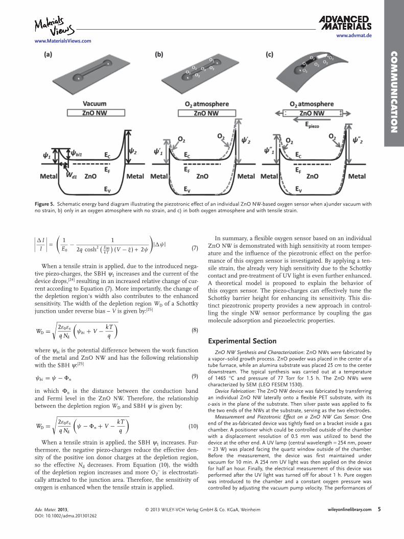
A possible explanation of the results presented in Figures 2 , 3 , and 4 can be interpreted by the piezotronic effect and gas adsorption on the ZnO NW, as shown in Figure 5 a–c. At thermal equilibrium, two Schottky barriers form at the con-tacts between the ZnO NW and the silver electrodes. Near the junctions, there are two depletion regions with positive donor ions. When oxygen is introduced into the chamber, at room temperature, the chemisorbed oxygen species on the ZnO NW are mainly O 2 − , accompanied by the electron transfer process given below: [ 22 , 23 ]
O2 + e− → O−2 (5)
This process forms an electron depletion layer at the NW surface and reduces the ZnO NW conductance. Furthermore, due to the electrostatic interaction, there is more chemisorbed O 2 − in the silver–ZnO Schottky junction area, where the posi-tive donor ions are present. [ 8 ] Therefore the SBH of each junc-tion increases and the overall current decreases, as shown in Figures 2 a, 2 b and 5 b.
When a strain is applied to this structure, owing to the non-central symmetric crystal structure of ZnO, a piezoelectric potential is created inside the ZnO NW. The piezopotential dis-tributes along the c -axis of the ZnO NW and net piezo-charges are presented at two ends of the ZnO NW. For the M-S-M structure, under positive or negative bias voltage, the transport properties are controlled only by the reversely biased Schottky junction. Take the device under positive bias as an example. The Schottky junction 1 is reversely biased and dominates the transport p roperty of the whole device. Therefore, Equation (2) is utilized to describe the performance of this device. According to Equation (2) , at a constant bias voltage, the change of current of this device due to exposure to oxygen is given by:
�I = S × �J = S × J
×(
1
2q cosh2 E00kT
)(V − ξ ) + 2ψ
− 1
E0
)�ψ
(6)
where S is the cross section area of this NW. Therefore, the magnitude of the relative change of current is given by:
mbH & Co. KGaA, Weinheim Adv. Mater. 2013, DOI: 10.1002/adma.201301262
www.advmat.dewww.MaterialsViews.com
CO
MM
UN
ICATIO
N
Figure 5 . Schematic energy band diagram illustrating the piezotronic effect of an individual ZnO NW-based oxygen sensor when a)under vacuum with no strain, b) only in an oxygen atmosphere with no strain, and c) in both oxygen atmosphere and with tensile strain.
I
I=
1
E0− 1
2q cosh2 E00kT
(V − ξ ) + 2| |
ψ
(7)
When a tensile strain is applied, due to the introduced nega-tive piezo-charges, the SBH ψ 1 increases and the current of the device drops, [ 24 ] resulting in an increased relative change of cur-rent according to Equation (7) . More importantly, the change of the depletion region's width also contributes to the enhanced sensitivity. The width of the depletion region W D of a Schottky junction under reverse bias – V is given by: [ 25 ]
WD =
√2ε0εs
q Nd
(ψbi + V − kT
q
)
(8)
where ψ bi is the potential difference between the work function of the metal and ZnO NW and has the following relationship with the SBH ψ : [ 25 ]
ψbi = ψ − �n (9)
in which Φ n is the distance between the conduction band and Fermi level in the ZnO NW. Therefore, the relationship between the depletion region W D and SBH ψ is given by:
WD =√
2ε0εs
q Nd
(ψ − �n + V − kT
q
)
(10)
When a tensile strain is applied, the SBH ψ 1 increases. Fur-thermore, the negative piezo-charges reduce the effective den-sity of the positive ion donor charges at the depletion region, so the effective N d decreases. From Equation (10) , the width of the depletion region increases and more O 2 − is electrostati-cally attracted to the junction area. Therefore, the sensitivity of oxygen is enhanced when the tensile strain is applied.
© 2013 WILEY-VCH Verlag GAdv. Mater. 2013, DOI: 10.1002/adma.201301262
In summary, a fl exible oxygen sensor based on an individual ZnO NW is demonstrated with high sensitivity at room temper-ature and the infl uence of the piezotronic effect on the perfor-mance of this oxygen sensor is investigated. By applying a ten-sile strain, the already very high sensitivity due to the Schottky contact and pre-treatment of UV light is even further enhanced. A theoretical model is proposed to explain the behavior of this oxygen sensor. The piezo-charges can effectively tune the Schottky barrier height for enhancing its sensitivity. This dis-tinct piezotronic property provides a new approach in control-ling the single NW sensor performance by coupling the gas molecule adsorption and piezoelectric properties.
Experimental Section ZnO NW Synthesis and Characterization : ZnO NWs were fabricated by
a vapor–solid growth process. ZnO powder was placed in the center of a tube furnace, while an alumina substrate was placed 25 cm to the center downstream. The typical synthesis was carried out at a temperature of 1465 ° C and pressure of 77 Torr for 1.5 h. The ZnO NWs were characterized by SEM (LEO FESEM 1530).
Device Fabrication : The ZnO NW device was fabricated by transferring an individual ZnO NW laterally onto a fl exible PET substrate, with its c -axis in the plane of the substrate. Then silver paste was applied to fi x the two ends of the NWs at the substrate, serving as the two electrodes.
Measurement and Piezotronic Effect on a ZnO NW Gas Sensor : One end of the as-fabricated device was tightly fi xed on a bracket inside a gas chamber. A positioner which could be controlled outside of the chamber with a displacement resolution of 0.5 mm was utilized to bend the device at the other end. A UV lamp (central wavelength = 254 nm, power = 23 W) was placed facing the quartz window outside of the chamber. Before the measurement, the device was fi rst maintained under vacuum for 10 min. A 254 nm UV light was then applied on the device for half an hour. Finally, the electrical measurement of this device was performed after the UV light was turned off for about 1 h. Pure oxygen was introduced to the chamber and a constant oxygen pressure was controlled by adjusting the vacuum pump velocity. The performances of
5wileyonlinelibrary.commbH & Co. KGaA, Weinheim

www.advmat.dewww.MaterialsViews.com
CO
MM
UN
ICATI
ON
the device under different strains and different oxygen pressures weremeasured by a computer-controlled measurement system.
Supporting Information Supporting Information is available from the Wiley Online Library or from the author.
Acknowledgements Research was supported by Airforce, U.S. Department of Energy, Offi ce of Basic Energy Sciences under Award DEFG02- 07ER46394, NSF, and the Knowledge Innovation Program of the Chinese Academy of Sciences (Grant KJCX2-YW-M13).
Received: March 20, 2013 Revised: April 22, 2013
Published online:
[ 1 ] N. S. Ramgir , Y. Yang , M. Zacharias , Small 2010 , 6 , 1705 . [ 2 ] A. Kolmakov , Y. X. Zhang , G. S. Cheng , M. Moskovits , Adv. Mater.
2003 , 15 , 997 . [ 3 ] Q. H. Li , Y. X. Liang , Q. Wan , T. H. Wang , Appl. Phys. Lett. 2004 , 85 ,
6389 . [ 4 ] C. Y. Lu , S. P. Chang , S. J. Chang , T. J. Hsueh , C. L. Hsu , Y. Z. Chiou ,
C. Chen , IEEE Sens. J. 2009 , 9 , 485 . [ 5 ] Z. Y. Fan , D. W. Wang , P. C. Chang , W. Y. Tseng , J. G. Lu , Appl. Phys.
Lett. 2004 , 85 , 5923 .
6 wileyonlinelibrary.com © 2013 WILEY-VCH Verlag
[ 6 ] Z. F. Liu , T. Yamazaki , Y. Shen , T. Kikuta , N. Nakatani , Y. X. Li , Sens. Actuators B 2008 , 129 , 666 .
[ 7 ] X. Y. Xue , P. Feng , Y. G. Wang , T. H. Wang , Appl. Phys. Lett. 2007 , 91 . [ 8 ] T. Y. Wei , P. H. Yeh , S. Y. Lu , Z. Lin-Wang , J. Am. Chem. Soc. 2009 ,
131 , 17690 . [ 9 ] Z. L. Wang , Nano Today 2010 , 5 , 540 . [ 10 ] Z. L. Wang , Adv. Mater. 2012 , 24 , 4632 . [ 11 ] J. Zhou , Y. D. Gu , P. Fei , W. J. Mai , Y. F. Gao , R. S. Yang , G. Bao ,
Z. L. Wang , Nano Lett. 2008 , 8 , 3035 . [ 12 ] R. M. Yu , C. F. Pan , Z. L. Wang , Energ. Environ. Sci. 2013 , 6 , 494 . [ 13 ] C. F. Pan , R. M. Yu , S. M. Niu , G. Zhu , Z. L. Wang , ACS Nano 2013 ,
7 , 1803 . [ 14 ] Z. W. Pan , Z. R. Dai , Z. L. Wang , Science 2001 , 291 , 1947 . [ 15 ] Y. F. Hu , Y. Liu , W. L. Li , M. Gao , X. L. Liang , Q. Li , L. M. Peng , Adv.
Funct. Mater. 2009 , 19 , 2380 . [ 16 ] L. M. Wu , F. F. Song , X. X. Fang , Z. X. Guo , S. Liang , Nanotech-
nology 2010 , 21 . [ 17 ] K. W. Liu , M. Sakurai , M. Aono , Sens. Actuators B 2011 , 157 , 98 . [ 18 ] Y. Liu , Z. Y. Zhang , Y. F. Hu , C. H. Jin , L. M. Peng , J. Nanosci. Nano-
technol. 2008 , 8 , 252 . [ 19 ] P. H. Yeh , Z. Li , Z. L. Wang , Adv. Mater. 2009 , 21 , 4975 . [ 20 ] J. Zhou , Y. D. Gu , Y. F. Hu , W. J. Mai , P. H. Yeh , G. Bao , A. K. Sood ,
D. L. Polla , Z. L. Wang , Appl. Phys. Lett. 2009 , 94 . [ 21 ] H. Q. Wang , N. Koshizaki , L. Li , L. C. Jia , K. Kawaguchi , X. Y. Li ,
A. Pyatenko , Z. Swiatkowska-Warkocka , Y. Bando , D. Golberg , Adv. Mater. 2011 , 23 , 1865 .
[ 22 ] D. H. Yoon , G. M. Choi , Sens. Actuators B 1997 , 45 , 251 . [ 23 ] M. Takata , D. Tsubone , H. Yanagida , J. Am. Ceram. Soc. 1976 , 59 , 4 . [ 24 ] Y. Zhang , Y. Liu , Z. L. Wang , Adv. Mater. 2011 , 23 , 3004 . [ 25 ] S. M. Sze , K. K. Ng , Physics of Semiconductor Devices , Wiley-Intersci-
ence , Hoboken, N.J. 2007 .
GmbH & Co. KGaA, Weinheim Adv. Mater. 2013, DOI: 10.1002/adma.201301262