enhancement of near-field radiative heat transfer using ... · enhancement of near-field radiative...
TRANSCRIPT

Enhancement of near-field radiative heat transferusing polar dielectric thin filmsBai Song1†, Yashar Ganjeh1†, Seid Sadat1†, Dakotah Thompson1, Anthony Fiorino1,Víctor Fernández-Hurtado2, Johannes Feist2, Francisco J. Garcia-Vidal2,3, Juan Carlos Cuevas2,Pramod Reddy1,4* and Edgar Meyhofer1*
Thermal radiative emission from a hot surface to a cold surfaceplays an important role in many applications, including energyconversion, thermal management, lithography, data storageand thermal microscopy1,2. Recent studies3–5 on bulk materialshave confirmed long-standing theoretical predictions indicatingthat when the gap between the surfaces is reduced to tens ofnanometres, well below the peak wavelength of the blackbodyemission spectrum, the radiative heat flux increases byorders of magnitude. However, despite recent attempts6,whether such enhancements can be obtained in nanoscaledielectric films thinner than the penetration depth of thermalradiation, as suggested by theory, remains experimentallyunknown. Here, using an experimental platform that comprisesa heat-flow calorimeter with a resolution of about 100 pW(ref. 7), we experimentally demonstrate a dramatic increasein near-field radiative heat transfer, comparable to thatobtained between bulk materials, even for very thin dielectricfilms (50–100 nm) when the spatial separation betweenthe hot and cold surfaces is comparable to the film thickness.We explain these results by analysing the spectral character-istics and mode shapes of surface phonon polaritons, whichdominate near-field radiative heat transport in polar dielectricthin films.
To experimentally study near-field radiative heat transfer(NFRHT) for a broad range of film thicknesses we developed anultra-sensitive, micro-fabricated calorimetric platform that enablesquantitative studies of gap-size-dependent heat currents from aspherical hot surface (the emitter) to a planar, colder surface (thereceiver) (Fig. 1). Understanding NFRHT is key to developingnovel technologies such as heat-assisted magnetic recording8 andlithography9 as well as near-field-based thermal management10–14.Despite long-standing theoretical predictions2,9,15–18, only recentlyhave measurements from bulk materials using either scanningprobes with integrated thermal sensors5 or bimaterial cantilever-based calorimeters3,4 provided experimental support of strikingenhancements in radiative heat transfer at the nanoscale. In spiteof this important progress, one of the most interesting theoreticalpredictions, which suggests that NFRHT in nanoscale gaps isdramatically enhanced by even nanometre-thick polar dielectricfilms18–21, has remained experimentally untested. In a recentexperimental report6 NFRHT was studied between a Au tip and aAu surface coated with a monolayer of NaCl, but the results wereinconclusive and seemed to defy theoretical interpretation, in partbecause an accurate measurement of heat currents could not becarried out.
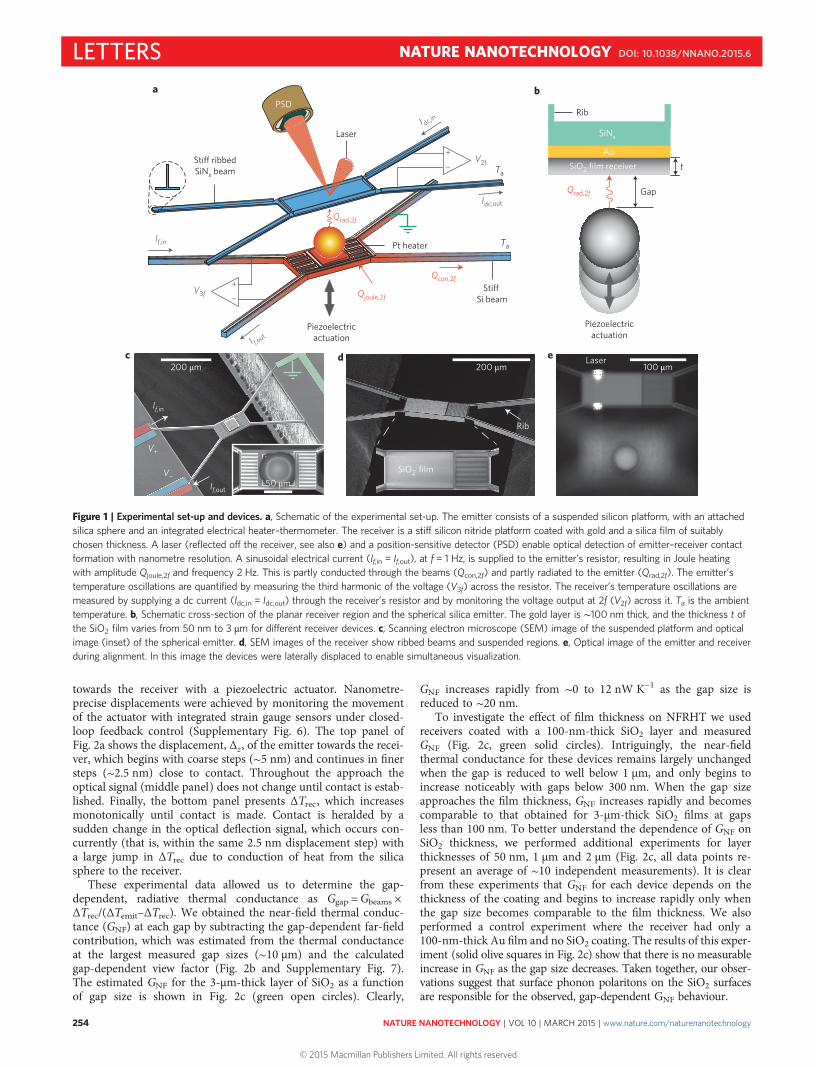
The experimental platform used in this work to study the filmthickness dependence of NFRHT is shown in Fig. 1. We preciselycontrolled the gap size between the spherical emitter and theplanar receiver to be as small as 20 nm to as large as 10 µm usinga custom-built nanopositioning platform22, while simultaneouslymeasuring heat currents between them to obtain the thermal con-ductance as a function of gap size. Contact between the emitterand the receiver was optically monitored (Fig. 1a). More specifically,the emitter device (Fig. 1a) consisted of a suspended silicon regiononto which a 53-μm-diameter silica (SiO2) sphere was attached(see Methods). The emitter also featured a platinum resistanceheater–thermometer through which a sinusoidal electric current( f = 1 Hz) was supplied to locally modulate the temperature of thesuspended region and the sphere at 2f (Supplementary Fig. 3).
The receiver (Fig. 1a,d) was made from silicon nitride (SiNx) andwas suspended via thin, long beams to achieve a thermal con-ductance (Gbeams) of ∼2 µW K−1. The planar suspended regionwas coated with SiO2 layers of varying thickness (50 nm–3 µm),deposited on a 100-nm-thick gold film (Fig. 1b,d). The receiveralso featured an integrated platinum resistance thermometer,which could resolve small temperature changes (∼50 µK, in a5 mHz bandwidth, when modulated at 2 Hz), enabling the detectionof small heat currents of ∼100 pW (2 µW K−1 × 50 µK).
Our experimental technique contributes several improvementsfor NFRHT measurements over previously used bimaterial cantile-ver-based approaches3,4, where the deflection of the bimaterial can-tilever is potentially affected by both temperature changes and forces(such as electrostatic or Casimir), posing challenges to the interpret-ation of experiments23. In contrast, in the present technique, mech-anical motion (detected optically) does not affect temperaturemeasurements that are performed independently with a resistancethermometer. Moreover, we are able to modulate the temperatureof the emitter and thus employ lock-in based techniques thatenhance7 the heat flow resolution to about 100 pW.
We began measurements with receivers coated with 3-μm-thicklayers of SiO2, which we expected to behave in a manner similar tobulk devices given their comparatively large thickness. After align-ing a receiver and emitter with a gap size of ∼10 µm in our nano-positioning platform22 (Fig. 1e), we moved the nanopositionerinto a vacuum chamber (<10−6 torr, room temperature) and modu-lated the emitter temperature (ΔTemit) sinusoidally at 2 Hz with a10 K amplitude. The resulting radiative heat currents were quanti-fied by measuring the temperature oscillations of the receiver(ΔTrec) using the integrated resistance thermometer. To measurethe gap dependence of the heat transfer we displaced the emitter
1Department of Mechanical Engineering, University of Michigan, Ann Arbor, Michigan 48109, USA. 2Departamento de Física Teórica de la MateriaCondensada and Condensed Matter Physics Center (IFIMAC), Universidad Autónoma de Madrid, Madrid 28049, Spain. 3Donostia InternationalPhysics Center (DIPC), Donostia/San Sebastián 20018, Spain. 4Department of Materials Science and Engineering, University of Michigan, Ann Arbor,Michigan 48109, USA. †These authors contributed equally to this paper. *e-mail: [email protected]; [email protected]
LETTERSPUBLISHED ONLINE: 23 FEBRUARY 2015 | DOI: 10.1038/NNANO.2015.6
NATURE NANOTECHNOLOGY | VOL 10 | MARCH 2015 | www.nature.com/naturenanotechnology 253
© 2015 Macmillan Publishers Limited. All rights reserved
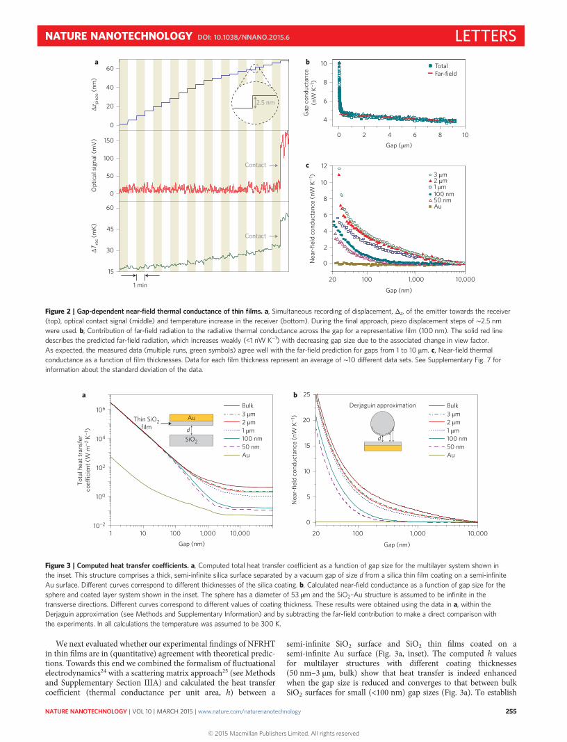
towards the receiver with a piezoelectric actuator. Nanometre-precise displacements were achieved by monitoring the movementof the actuator with integrated strain gauge sensors under closed-loop feedback control (Supplementary Fig. 6). The top panel ofFig. 2a shows the displacement, Δz , of the emitter towards the recei-ver, which begins with coarse steps (∼5 nm) and continues in finersteps (∼2.5 nm) close to contact. Throughout the approach theoptical signal (middle panel) does not change until contact is estab-lished. Finally, the bottom panel presents ΔTrec , which increasesmonotonically until contact is made. Contact is heralded by asudden change in the optical deflection signal, which occurs con-currently (that is, within the same 2.5 nm displacement step) witha large jump in ΔTrec due to conduction of heat from the silicasphere to the receiver.
These experimental data allowed us to determine the gap-dependent, radiative thermal conductance as Ggap =Gbeams ×ΔTrec/(ΔTemit–ΔTrec). We obtained the near-field thermal conduc-tance (GNF) at each gap by subtracting the gap-dependent far-fieldcontribution, which was estimated from the thermal conductanceat the largest measured gap sizes (∼10 µm) and the calculatedgap-dependent view factor (Fig. 2b and Supplementary Fig. 7).The estimated GNF for the 3-µm-thick layer of SiO2 as a functionof gap size is shown in Fig. 2c (green open circles). Clearly,
GNF increases rapidly from ∼0 to 12 nW K−1 as the gap size isreduced to ∼20 nm.
To investigate the effect of film thickness on NFRHT we usedreceivers coated with a 100-nm-thick SiO2 layer and measuredGNF (Fig. 2c, green solid circles). Intriguingly, the near-fieldthermal conductance for these devices remains largely unchangedwhen the gap is reduced to well below 1 µm, and only begins toincrease noticeably with gaps below 300 nm. When the gap sizeapproaches the film thickness, GNF increases rapidly and becomescomparable to that obtained for 3-μm-thick SiO2 films at gapsless than 100 nm. To better understand the dependence of GNF onSiO2 thickness, we performed additional experiments for layerthicknesses of 50 nm, 1 µm and 2 µm (Fig. 2c, all data points re-present an average of ∼10 independent measurements). It is clearfrom these experiments that GNF for each device depends on thethickness of the coating and begins to increase rapidly only whenthe gap size becomes comparable to the film thickness. We alsoperformed a control experiment where the receiver had only a100-nm-thick Au film and no SiO2 coating. The results of this exper-iment (solid olive squares in Fig. 2c) show that there is no measurableincrease in GNF as the gap size decreases. Taken together, our obser-vations suggest that surface phonon polaritons on the SiO2 surfacesare responsible for the observed, gap-dependent GNF behaviour.
200 μm
Rib
SiO2 film
Laser200 μm
c
If,in
V+
V−If,out
Piezoelectricactuation
Stiff Si beam
V3f
If,in
Idc,out
Pt heater
PSD
Laser
Stiff ribbedSiNx beam
+−
V2f
a
I dc,in
I f,out
Qjoule,2f
Qrad,2f
Qcon,2f
Ta
Ta
+−
b
tSiO2 film receiverAu
SiNx
Rib
Qrad,2f
Piezoelectricactuation
d e
50 μm
100 μm
Gap
Figure 1 | Experimental set-up and devices. a, Schematic of the experimental set-up. The emitter consists of a suspended silicon platform, with an attachedsilica sphere and an integrated electrical heater–thermometer. The receiver is a stiff silicon nitride platform coated with gold and a silica film of suitablychosen thickness. A laser (reflected off the receiver, see also e) and a position-sensitive detector (PSD) enable optical detection of emitter–receiver contactformation with nanometre resolution. A sinusoidal electrical current (If,in = If,out), at f = 1 Hz, is supplied to the emitter’s resistor, resulting in Joule heatingwith amplitude Qjoule,2f and frequency 2 Hz. This is partly conducted through the beams (Qcon,2f) and partly radiated to the emitter (Qrad,2f). The emitter’stemperature oscillations are quantified by measuring the third harmonic of the voltage (V3f) across the resistor. The receiver’s temperature oscillations aremeasured by supplying a dc current (Idc,in = Idc,out) through the receiver’s resistor and by monitoring the voltage output at 2f (V2f) across it. Ta is the ambienttemperature. b, Schematic cross-section of the planar receiver region and the spherical silica emitter. The gold layer is ∼100 nm thick, and the thickness t ofthe SiO2 film varies from 50 nm to 3 µm for different receiver devices. c, Scanning electron microscope (SEM) image of the suspended platform and opticalimage (inset) of the spherical emitter. d, SEM images of the receiver show ribbed beams and suspended regions. e, Optical image of the emitter and receiverduring alignment. In this image the devices were laterally displaced to enable simultaneous visualization.
LETTERS NATURE NANOTECHNOLOGY DOI: 10.1038/NNANO.2015.6
NATURE NANOTECHNOLOGY | VOL 10 | MARCH 2015 | www.nature.com/naturenanotechnology254
© 2015 Macmillan Publishers Limited. All rights reserved
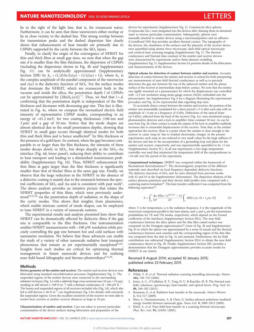
We next evaluated whether our experimental findings of NFRHTin thin films are in (quantitative) agreement with theoretical predic-tions. Towards this end we combined the formalism of fluctuationalelectrodynamics24 with a scattering matrix approach25 (see Methodsand Supplementary Section IIIA) and calculated the heat transfercoefficient (thermal conductance per unit area, h) between a
semi-infinite SiO2 surface and SiO2 thin films coated on asemi-infinite Au surface (Fig. 3a, inset). The computed h valuesfor multilayer structures with different coating thicknesses(50 nm–3 µm, bulk) show that heat transfer is indeed enhancedwhen the gap size is reduced and converges to that between bulkSiO2 surfaces for small (<100 nm) gap sizes (Fig. 3a). To establish
Nea
r-fie
ld c
ondu
ctan
ce (n
W K
−1)
20 100 1,000 10,000
Gap (nm)
12
10
8
6
4
2
0
Au50 nm100 nm1 μm2 μm3 μm
c
Gap
con
duct
ance
(nW
K−1
)
b
2 4 6 8 10
Gap (μm)
10
8
6
4
0
a
Δzpi
ezo (
nm)
Opt
ical
sig
nal (
mV
)ΔT
rec
(mK)
1 min
2.5 nm
60
40
20
0
150
100
50
0
60
45
30
15
TotalFar-field
Contact
Contact
Figure 2 | Gap-dependent near-field thermal conductance of thin films. a, Simultaneous recording of displacement, Δz, of the emitter towards the receiver(top), optical contact signal (middle) and temperature increase in the receiver (bottom). During the final approach, piezo displacement steps of ∼2.5 nmwere used. b, Contribution of far-field radiation to the radiative thermal conductance across the gap for a representative film (100 nm). The solid red linedescribes the predicted far-field radiation, which increases weakly (<1 nW K−1) with decreasing gap size due to the associated change in view factor.As expected, the measured data (multiple runs, green symbols) agree well with the far-field prediction for gaps from 1 to 10 µm. c, Near-field thermalconductance as a function of film thicknesses. Data for each film thickness represent an average of ∼10 different data sets. See Supplementary Fig. 7 forinformation about the standard deviation of the data.
100 1,000
0
5
10
15
20
25
Nea
r-fie
ld c
ondu
ctan
ce (n
W K
−1)
Gap (nm)
Derjaguin approximation
d
1 10 100 1,000 10,00010−2
100
102
104
106
Tota
l hea
t tra
nsfe
r co
effici
ent (
W m
−2 K
−1)
Gap (nm)
dSiO2
Au
a b
Thin SiO2film
10,000
Au50 nm100 nm1 μm2 μm3 μmBulk
Au50 nm100 nm1 μm2 μm3 μmBulk
20
Figure 3 | Computed heat transfer coefficients. a, Computed total heat transfer coefficient as a function of gap size for the multilayer system shown inthe inset. This structure comprises a thick, semi-infinite silica surface separated by a vacuum gap of size d from a silica thin film coating on a semi-infiniteAu surface. Different curves correspond to different thicknesses of the silica coating. b, Calculated near-field conductance as a function of gap size for thesphere and coated layer system shown in the inset. The sphere has a diameter of 53 µm and the SiO2–Au structure is assumed to be infinite in thetransverse directions. Different curves correspond to different values of coating thickness. These results were obtained using the data in a, within theDerjaguin approximation (see Methods and Supplementary Information) and by subtracting the far-field contribution to make a direct comparison withthe experiments. In all calculations the temperature was assumed to be 300 K.
NATURE NANOTECHNOLOGY DOI: 10.1038/NNANO.2015.6 LETTERS
NATURE NANOTECHNOLOGY | VOL 10 | MARCH 2015 | www.nature.com/naturenanotechnology 255
© 2015 Macmillan Publishers Limited. All rights reserved

a direct comparison with our experimental results, we computed thenear-field conductance between a 53-μm-diameter silica sphere andthin film-coated surfaces (Fig. 3b) via the Derjaguin approxi-mation26 (see Methods). The predicted conductances, as a functionof gap size and film thickness, are in good overall agreement withour measurements (cf. Figs 2c and 3b), although the calculated con-ductances consistently overestimate the measured thermal conduc-tance (see Supplementary Fig. 12 for a direct comparison). As wedemonstrate in Supplementary Section IIIC and SupplementaryFig. 13, these deviations are not due to the use of the Derjaguinapproximation, which provides accurate results for the NFRHT inour systems in spite of the nanometre-scale roughness of thefilms. Instead, we attribute this comparatively small discrepancy tothe inevitable uncertainties associated with the microstructure andoptical properties of the integrated thin films. Overall, the observedagreement between measurements and theoretical predictionssuggests that fluctuational electrodynamics successfully capturesthe key aspects of the gap-dependent NFRHT in these thin-film
structures and raises the key question: what is the origin of thefilm thickness dependence of GNF?
To elucidate the origin of the thickness dependence of the NFRHTwe compared (for two multilayer configurations with 100-nm- and3-µm-thick SiO2 films and 20 nm gaps) the calculated spectral heattransfer coefficients hs(ω) and hp(ω) for the transverse electric (TE)and transverse magnetic (TM) modes, respectively (Fig. 4a andSupplementary Fig. 9). It can be seen that TM modes dominateheat transfer at small gap sizes, with major contributions from twonarrow energy ranges centred around ∼0.06 eV and ∼0.14 eV. Todetermine which modes dominate the heat flux we plot in Fig. 4bthe transmission probability (see Methods) for the TM modes,which depends on both the frequency (ω) and the magnitude (k)of the parallel component of the wavevector.We also overlay the com-puted dispersion relationship for cavity surface phonon polaritons(CSPhPs, dashed line) and the light line (solid line) on this plot. Itcan be seen that the transmission probability is largest in the afore-mentioned energy ranges (Fig. 4b) and occurs for wavevectors that
0.75
0.50
0.25
0.00
1.00
0 1 2 3 4 5 6 7
0.06
0.08
0.10
0.12
0.14
0.16
0.0
0.5
1.0
Nor
mal
ized
IEI2
Nor
mal
ized
IEI2
Nor
mal
ized
IEI2
Nor
mal
ized
IEI2
0.0
0.5
1.0
0.0
0.5
1.0
0.0
0.5
1.0
20 nm
20 nm
SiO2 SiO2 (3 μm)
SiO2SiO2 Au AuSiO2
SiO2
SiO2
SiO2
100 nm
100 nm
c d
Spec
tral
hea
t tra
nsfe
r co
effici
ent (
W e
V−1
m−2
K−1
)
100 nm, TE100 nm, TM3 μm, TE3 μm, TM
a b
0.02
10−2
100
102
104
106
0.08 0.14 0.20
k (107 m−1)
−150 −100 −50 0 50 100 150
Z (nm)
−150 −100 −50 0 50 100 150
Z (nm)
−300 −200 −100 0 100 200 300
Z (nm)
−300 −200 −100 0 100 200 300
Z (nm)
Light line
(3 μm)
(100 nm)(100 nm)
ħω (eV)
ħω (e
V)
τp (ω, k)
Figure 4 | Role of surface phonon polaritons in near-field radiative heat transfer. a, Spectral heat transfer coefficient for TE and TM modes as a function ofradiation energy for the multilayer system in Fig. 3a with coating thicknesses of t= 100 nm (solid lines) and t= 3 µm (dashed lines) at a gap of 20 nm. Theheat transfer is dominated by TM modes and their contribution is almost identical for both thicknesses. Z represents the distance from the centre of the gap.b, Corresponding transmission probability for TM modes, τp(ω, k), as a function of radiation energy and magnitude of the parallel wavevector for t = 100 nmand d = 20 nm. The white dashed line corresponds to the analytical dispersion relation of the cavity surface phonon polaritons, and the pink solid line next tothe y-axis represents the light line, that is, ω = kc. The maxima of the transmission appear largely to the right of the light line and therefore correspond toevanescent waves. c, Normalized electric field intensity of a representative cavity surface phonon polariton (CSPhP) mode (ħω = 61.2 meV) for a gap of20 nm and thicknesses of t= 3 µm (upper panel) and t= 100 nm (lower panel), normalized to peak intensity. Grey regions correspond to SiO2 and theyellow region represents Au. d, As in c, but for a gap of 100 nm.
LETTERS NATURE NANOTECHNOLOGY DOI: 10.1038/NNANO.2015.6
NATURE NANOTECHNOLOGY | VOL 10 | MARCH 2015 | www.nature.com/naturenanotechnology256
© 2015 Macmillan Publishers Limited. All rights reserved
lie to the right of the light line, that is, for evanescent waves.Furthermore, it can be seen that these wavevectors either overlap orlie in close vicinity to the dashed line. This strong overlap betweenthe transmission peaks and the dashed dispersion line clearlyshows that enhancements of heat transfer are primarily due toCSPhPs supported by the cavity between the SiO2 layers.
Finally, to clarify the origin of the convergence of NFRHT forthin and thick films at small gap sizes, we note that when the gapsize d is smaller than the film thickness, the dispersion of CSPhPs(including the dispersions shown in Fig. 4b and SupplementaryFig. 11) can be analytically approximated (SupplementarySection IIIB) by kC = (1/d) ln ((ε(ω) − 1)/(ε(ω) + 1)), where kC isthe complex amplitude of the parallel component of the wavevectorand ε(ω) is the dielectric function of SiO2. For the surface modesthat dominate the NFRHT, which are evanescent both in thevacuum and inside the silica, the penetration depth l of CSPhPscan be approximated by [2Re{kC(ω)}]
−1. Thus, we find that l ≈ d,confirming that the penetration depth is independent of the filmthickness and decreases with decreasing gap size. This fact is illus-trated in Fig. 4c, where we compare the normalized electric fieldintensity of representative CSPhP modes, corresponding to anenergy of ∼61.2 meV, for two coating thicknesses (100 nm and3 µm) and a gap of 20 nm. Notice that the mode shapes arealmost identical due to the small penetration depths, showing thatNFRHT in small gaps occurs through identical modes for boththin and thick films and is hence unaffected27 by film thickness orthe presence of a gold layer. In contrast, when the gap becomes com-parable to or larger than the film thickness, the intensity of thesemodes decays slowly in SiO2, but drops sharply at the SiO2–Auinterface (Fig. 4d, lower panel), reducing their ability to contributeto heat transport and leading to a diminished transmission prob-ability (Supplementary Fig. 10). Thus, NFRHT enhancement forthin films at gaps larger than the film thickness is significantlysmaller than that of thicker films at the same gap size. Finally, weobserve that the large reduction in the NFRHT in the absence ofa dielectric coating is mainly due to the mismatch between the spec-tral coefficients of SiO2 and Au and is consistent with past work4.The above analysis provides an intuitive picture that relates theNFRHT properties of thin films, which were previously under-stood19,21,28 via the penetration depth of radiation, to the shape ofthe cavity modes. This shows that insights from plasmonics,which enable intricate control of mode shapes, can be employedto tune NFRHT in a variety of nanoscale systems.
The experimental results and analysis presented here show thatNFRHT can be dramatically affected by dielectric films if the gapsize is comparable to the film thickness. Our instrumentationenables NFRHT measurements with ∼100 pW resolution while pre-cisely controlling the gap size between hot and cold surfaces withnanometre resolution. We believe that these advances can enablethe study of a variety of other nanoscale radiative heat transportphenomena that remain as yet experimentally unexplored14,29.Insights from such studies are critical for optimizing thermalmanagement in future nanoscale devices and for realizingnear-field-based lithography and thermo-photovoltaics9,12,30.
MethodsDevice geometry of the emitter and receiver. The emitter and receiver devices werefabricated using standard microfabrication processes (Supplementary Fig. 1). Thesuspended regions of the emitter devices were connected to the surroundingsubstrate via beams (Fig. 1c) with a relatively large cross-sectional area (10 µm × 10 µm),resulting in stiff devices (∼500 N m−1) with a thermal conductance of ∼180 µW K−1.The beams and suspended regions of all receivers included ribs (Fig. 1d), which alsoled to stiff devices (∼66 N m−1; see Supplementary Fig. 4 for details) with extremelyflat suspended regions. Given the excellent sensitivity of the receiver we were able toresolve heat currents at emitter–receiver distances as large as 10 µm.
Characterization of emitter and receiver. Care was taken to prevent particulatecontamination of the device surfaces during fabrication and preparation of the
devices for experiments (Supplementary Fig. 2). Commercial silica spheres(Corpuscular Inc.) were integrated into the devices after cleaning them in deionizedwater to remove particulate contamination. Subsequently, spheres weremanually attached to emitter devices using a micromanipulator and an adhesive(Crystalbond 509) that provides excellent thermal contact. The topography ofthe devices, the cleanliness of the surfaces and the planarity of the receiver devicewere quantified using atomic force microscopy, dark-field optical microscopyand confocal laser scanning imaging (Supplementary Fig. 5). The thermalconductance and thermal time constant of the emitter and receiver deviceswere characterized by experiments and/or finite-element modelling(Supplementary Fig. 3). Supplementary Section IA presents details of the fabricationand characterization of the devices.
Optical scheme for detection of contact between emitter and receiver. Accuratedetection of contact between the emitter and receiver is critical for both interpretingour measurements of near-field thermal conductance as well as to preciselydetermine the gap size between the top of the spherical emitter and the planarsurface of the receiver at intermediate steps before contact. We note that the emitterwas rigidly mounted on a piezoactuator for which the displacement was controlledwith ∼2.5 nm resolution using strain-gauge sensors (SGSs) embedded into thepiezoactuator. See Supplementary Fig. 6 for a diagram illustrating the experimentalprocedure and Fig. 2a for experimental data regarding step sizes.
To accurately detect contact between the emitter and receiver, the position of theemitter was sinusoidally modulated for a short period (∼5 s) after each step with anamplitude of ∼4 nm at a frequency of 4 kHz. Deflections of the optical beam(at 4 kHz), reflected from the back of the receiver (Fig. 1a), were monitored using aphotosensitive detector and a lock-in amplifier (time constant 30 ms). As can beseen from Fig. 2b, when contact is made the output of the lock-in amplifier suddenlyincreases due to sinusoidal displacements of the receiver. Note that, as the emitterapproaches the receiver, there is a point where the emitter is close enough to thereceiver to cause ‘snap-in’ due to residual electrostatic charges. In the presentexperiments, such snap-in was reduced to very small values by the large stiffness ofthe devices and due to the incorporation of a grounding loop and plane for theemitter and receiver, respectively, and was experimentally quantified to be <5 nm(Supplementary Section IC). In all our experiments a two-stage temperaturecontroller was used that minimized the temperature drift of the nanopositioner to<10 mK over the period of the experiment.
Computational techniques. NFRHT was computed within the framework offluctuational electrodynamics24. The electromagnetic properties of the differentmaterials were described via local frequency-dependent dielectric functions.The dielectric functions of SiO2 and Au were obtained from previous works(refs 42 and 43 in the Supplementary Information). The dispersion relations of thesurface phonon polaritons and their electric field profiles were computed with ascattering matrix formalism25. The heat transfer coefficient h was computed from thefollowing expression19:
h =∫∞0
dω4π2
∂[h�ω / (eh�ω/kBT − 1)]∂T
∫∞0dkk[τs(ω, k) + τp(ω, k)] (1)
where T is the temperature, ω is the radiation frequency, k is the magnitude of thewavevector component parallel to the layer planes, and τs and τp are the transmissionprobabilities for TE and TM modes, respectively, which depend on the Fresnelcoefficients of the interfaces (Supplementary Section IIIA). The near-fieldconductance between the silica sphere and the thin film-coated surface wascomputed via the Derjaguin approximation26 (inset of Fig. 3b and SupplementaryFig. 8) in which the sphere was approximated by a series of annuli and the thermalconductance between each annulus and the corresponding region of the thin filmwas computed from the data in Fig. 3a and summed. Furthermore, the far-fieldcontribution was subtracted (Supplementary Section IIIA) to obtain the near-fieldconductance shown in Fig. 3b. Finally, Supplementary Section IIIC provides ademonstration that the Derjaguin approximation provides accurate results forNFRHT in our system.
Received 8 August 2014; accepted 10 January 2015;published online 23 February 2015
References1. Wilde, Y. D. et al. Thermal radiation scanning tunnelling microscopy. Nature
444, 740–743 (2006).2. Jones, A. C., O’Callahan, B. T., Yang, H. U. & Raschke, M. B. The thermal near-
field: coherence, spectroscopy, heat-transfer, and optical forces. Prog. Surf. Sci.88, 349–392 (2013).
3. Rousseau, E. et al. Radiative heat transfer at the nanoscale. Nature Photon.3, 514–517 (2009).
4. Shen, S., Narayanaswamy, A. & Chen, G. Surface phonon polaritons mediatedenergy transfer between nanoscale gaps. Nano Lett. 9, 2909–2913 (2009).
5. Kittel, A. et al. Near-field heat transfer in a scanning thermal microscope.Phys. Rev. Lett. 95, 224301 (2005).
NATURE NANOTECHNOLOGY DOI: 10.1038/NNANO.2015.6 LETTERS
NATURE NANOTECHNOLOGY | VOL 10 | MARCH 2015 | www.nature.com/naturenanotechnology 257
© 2015 Macmillan Publishers Limited. All rights reserved

6. Worbes, L., Hellmann, D. & Kittel, A. Enhanced near-field heat flow of amonolayer dielectric island. Phys. Rev. Lett. 110, 134302 (2013).
7. Sadat, S., Meyhofer, E. & Reddy, P. Resistance thermometry-based picowatt-resolution heat-flow calorimeter. Appl. Phys. Lett. 102, 163110 (2013).
8. Challener, W. A. et al. Heat-assisted magnetic recording by a near-fieldtransducer with efficient optical energy transfer. Nature Photon. 3,220–224 (2009).
9. Pendry, J. B. Radiative exchange of heat between nanostructures. J. Phys.Condens. Matter 11, 6621–6633 (1999).
10. Otey, C., Lau, W. T. & Fan, S. Thermal rectification through vacuum. Phys. Rev.Lett. 104, 154301 (2010).
11. Rodriguez, A. W. et al. Frequency-selective near-field radiative heat transferbetween photonic crystal slabs: a computational approach for arbitrarygeometries and materials. Phys. Rev. Lett. 107, 114302 (2011).
12. Guha, B., Otey, C., Poitras, C. B., Fan, S. H. & Lipson, M. Near-field radiativecooling of nanostructures. Nano Lett. 12, 4546–4550 (2012).
13. Van Zwol, P. J., Ranno, L. & Chevrier, J. Tuning near field radiative heatflux through surface excitations with a metal insulator transition. Phys. Rev. Lett.108, 234301 (2012).
14. Ben-Abdallah, P. & Biehs, S. A. Near-field thermal transistor. Phys. Rev. Lett.112, 044301 (2014).
15. Polder, D. & Hove, M. A. V. Theory of radiative heat transfer between closelyspaced bodies. Phys. Rev. B 4, 3303–3314 (1971).
16. Joulain, K., Mulet, J-P., Marquier, F., Carminati, R. & Greffet, J-J. Surfaceelectromagnetic waves thermally excited: radiative heat transfer, coherenceproperties and Casimir forces revisited in the near field. Surf. Sci. Rep.57, 59–112 (2005).
17. Volokitin, A. I. & Persson, B. N. J. Near-field radiative heat transfer andnoncontact friction. Rev. Mod. Phys. 79, 1291–1329 (2007).
18. Basu, S., Zhang, Z. & Fu, C. Review of near-field thermal radiation and itsapplication to energy conversion. Int. J. Energ. Res. 33, 1203–1232 (2009).
19. Biehs, S. A. Thermal heat radiation, near-field energy density and near-fieldradiative heat transfer of coated materials. Eur. Phys. J. B 58, 423–431 (2007).
20. Francoeur, M., Menguc, M. P. & Vaillon, R. Coexistence of multiple regimes fornear-field thermal radiation between two layers supporting surface phononpolaritons in the infrared. Phys. Rev. B 84, 075436 (2011).
21. Basu, S. & Zhang, Z. M. Ultrasmall penetration depth in nanoscale thermalradiation. Appl. Phys. Lett. 95, 133104 (2009).
22. Ganjeh, Y. et al. A platform to parallelize planar surfaces and control their spatialseparation with nanometer resolution. Rev. Sci. Instrum. 83, 105101 (2012).
23. Cahill, D. G. et al. Nanoscale thermal transport. II. 2003–2012. Appl. Phys. Rev.1, 011305 (2014).
24. Rytov, S. M., Kravtsov, I. A. & Tatarskii, V. I. Principles of Statistical Radiophysics2nd edn, Vol. 3 (Springer-Verlag, 1987).
25. Whittaker, D. M. & Culshaw, I. S. Scattering-matrix treatment of patternedmultilayer photonic structures. Phys. Rev. B 60, 2610–2618 (1999).
26. Derjaguin, B. V., Abrikosova, I. I. & Lifshitz, E. M. Direct measurement ofmolecular attraction between solids separated by a narrow gap. Q. Rev. Chem.Soc. 10, 295–329 (1956).
27. Biehs, S. A., Rousseau, E. & Greffet, J. J. Mesoscopic description of radiative heattransfer at the nanoscale. Phys. Rev. Lett. 105, 234301 (2010).
28. Francoeur, M., Menguc, M. P. & Vaillon, R. Near-field radiative heat transferenhancement via surface phonon polaritons coupling in thin films. Appl. Phys.Lett. 93, 043109 (2008).
29. Rodriguez, A. W. et al. Anomalous near-field heat transfer between a cylinderand a perforated surface. Phys. Rev. Lett. 110, 014301 (2013).
30. Lenert, A. et al. A nanophotonic solar thermophotovoltaic device. NatureNanotech. 9, 126–130 (2014).
AcknowledgementsP.R. and E.M. acknowledge support from the Army Research Office (W911NF-12-1-0612;device fabrication) and the National Science Foundation (CBET 1235691; instrumentationand measurements). J.C.C. acknowledges financial support from the Spanish MICINN(contract no. FIS2011-28851-C02-01) and thanks E. Moreno for helpful discussions.V.F-H. acknowledges financial support from ‘la Caixa’ Foundation. F.J.G-V. and J.F.acknowledge support from the European Research Council (ERC-2011-AdG proposal no.290981). The authors acknowledge the Lurie Nanofabrication Facility (LNF) for facilitatingthe nanofabrication of devices.
Author contributionsThe work was conceived by P.R. and E.M. The experiments were performed by B.S., Y.G.and A.F. under supervision by E.M. and P.R. The devices were designed and fabricated byS.S., D.T. and B.S. Modelling was performed by V.F-H. and J.F. under the supervision ofF.J.G-V. and J.C.C. The manuscript was written by P.R., E.M. and J.C.C. with commentsand input from all authors.
Additional informationSupplementary information is available in the online version of the paper. Reprints andpermissions information is available online at www.nature.com/reprints. Correspondence andrequests for materials should be addressed to P.R. and E.M.
Competing financial interestsThe authors declare no competing financial interests.
LETTERS NATURE NANOTECHNOLOGY DOI: 10.1038/NNANO.2015.6
NATURE NANOTECHNOLOGY | VOL 10 | MARCH 2015 | www.nature.com/naturenanotechnology258
© 2015 Macmillan Publishers Limited. All rights reserved