enhancement of ultrahigh rate chargeability by interfacial
TRANSCRIPT
Enhancement of Ultrahigh Rate Chargeability by Interfacial NanodotBaTiO3 Treatment on LiCoO2 Cathode Thin Film BatteriesSou Yasuhara,†,∥ Shintaro Yasui,*,†,∥ Takashi Teranishi,‡,∥ Keisuke Chajima,‡ Yumi Yoshikawa,‡
Yutaka Majima,† Tomoyasu Taniyama,†,§ and Mitsuru Itoh*,†
†Laboratory for Materials and Structures, Tokyo Institute of Technology, Yokohama 226-8503, Japan‡Graduate School of Natural Science and Technology, Okayama University, Okayama 700-8530, Japan§Department of Physics, Nagoya University, Nagoya 464-8601, Japan
*S Supporting Information
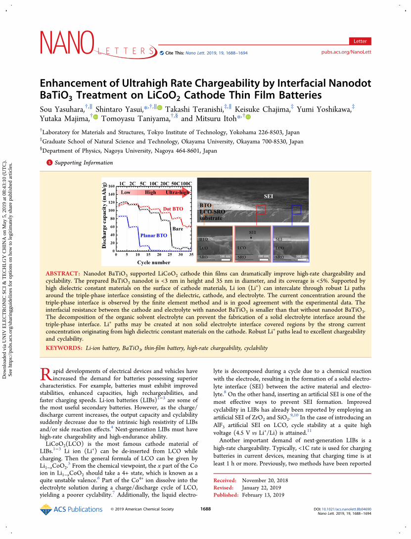
ABSTRACT: Nanodot BaTiO3 supported LiCoO2 cathode thin films can dramatically improve high-rate chargeability andcyclability. The prepared BaTiO3 nanodot is <3 nm in height and 35 nm in diameter, and its coverage is <5%. Supported byhigh dielectric constant materials on the surface of cathode materials, Li ion (Li+) can intercalate through robust Li pathsaround the triple-phase interface consisting of the dielectric, cathode, and electrolyte. The current concentration around thetriple-phase interface is observed by the finite element method and is in good agreement with the experimental data. Theinterfacial resistance between the cathode and electrolyte with nanodot BaTiO3 is smaller than that without nanodot BaTiO3.The decomposition of the organic solvent electrolyte can prevent the fabrication of a solid electrolyte interface around thetriple-phase interface. Li+ paths may be created at non solid electrolyte interface covered regions by the strong currentconcentration originating from high dielectric constant materials on the cathode. Robust Li+ paths lead to excellent chargeabilityand cyclability.
KEYWORDS: Li-ion battery, BaTiO3, thin-film battery, high-rate chargeability, cyclability
Rapid developments of electrical devices and vehicles haveincreased the demand for batteries possessing superior
characteristics. For example, batteries must exhibit improvedstabilities, enhanced capacities, high rechargeabilities, andfaster charging speeds. Li-ion batteries (LIBs)1−3 are some ofthe most useful secondary batteries. However, as the charge/discharge current increases, the output capacity and cyclabilitysuddenly decrease due to the intrinsic high resistivity of LIBsand/or side reaction effects.4 Next-generation LIBs must havehigh-rate chargeability and high-endurance ability.LiCoO2(LCO) is the most famous cathode material of
LIBs.1−3 Li ion (Li+) can be de-inserted from LCO whilecharging. Then the general formula of LCO can be given byLi1−xCoO2.
5 From the chemical viewpoint, the x part of the Coion in Li1−xCoO2 should take a 4+ state, which is known as aquite unstable valence.6 Part of the Co4+ ion dissolve into theelectrolyte solution during a charge/discharge cycle of LCO,yielding a poorer cyclability.7 Additionally, the liquid electro-
lyte is decomposed during a cycle due to a chemical reactionwith the electrode, resulting in the formation of a solid electro-lyte interface (SEI) between the active material and electro-lyte.8 On the other hand, inserting an artificial SEI is one of themost effective ways to prevent SEI formation. Improvedcyclability in LIBs has already been reported by employing anartificial SEI of ZrO2 and SiO2.
9,10 In the case of introducing anAlF3 artificial SEI on LCO, cycle stability at a quite highvoltage (4.5 V vs Li+/Li) is attained.11
Another important demand of next-generation LIBs is ahigh-rate chargeability. Typically, <1C rate is used for chargingbatteries in current devices, meaning that charging time is atleast 1 h or more. Previously, two methods have been reported
Received: November 20, 2018Revised: January 22, 2019Published: February 13, 2019
Letter
pubs.acs.org/NanoLettCite This: Nano Lett. 2019, 19, 1688−1694
© 2019 American Chemical Society 1688 DOI: 10.1021/acs.nanolett.8b04690Nano Lett. 2019, 19, 1688−1694
Dow
nloa
ded
via
UN
IV E
LE
CT
RO
NIC
SC
I &
TE
CH
LG
Y C
HIN
A o
n M
ay 5
, 201
9 at
08:
43:1
0 (U
TC
).
See
http
s://p
ubs.
acs.
org/
shar
ingg
uide
lines
for
opt
ions
on
how
to le
gitim
atel
y sh
are
publ
ishe
d ar
ticle
s.

to improve the high-rate characteristic in the cathodematerials: the grain size reduction method and the surface
modification method. The former (e.g., use of nanoparticlecathodes)12 can realize shorter Li+ diffusion lengths and larger
Figure 1. (a) Schematic of the calculated model structure of BTO-LCO with ANSYS HFSS. (b) Calculated current density mapping on an LCOsurface. (c) Schematic three-dimensional images of Bare, Planar BTO, and Dot BTO. (d−f) Surface SEM images of Bare (d), Planar BTO (e), andDot BTO (f). (g) Cross-sectional STEM images. Inset is an expansion of the red dashed square. (h) Height scan result of 1 BTO dot with DotBTO by AFM.
Nano Letters Letter
DOI: 10.1021/acs.nanolett.8b04690Nano Lett. 2019, 19, 1688−1694
1689

surface areas in nanoparticle cathodes. The latter (e.g., atomiclayered Al2O3 decoration on the cathode surface)13 canprevent the elution of cobalt ion into an electrolyte. Recently,Teranishi et al. reported a high-rate capability in an LCOcathode supported ferroelectric BaTiO3 (BTO).14 Thedischarge capacity of BTO supported LCO after 10C is 150mAh/g, which is approximately 80% of the value at 0.1C. Thehigh rate performance was enhanced by modifying the cathodeusing high dielectric constant materials.15 However, thedetailed mechanism of this improvement, especially theinterfacial conditions under charge/discharge, remains unclear.In the present study, we focused on the BTO−LCO interfaceto investigate the effect of ferroelectric modifications on thehigh-rate chargeability in cathode materials using the finiteelement method (FEM) and the preparation of thin-filmbatteries.We calculated the current density at the LCO surface, on
which one BTO dot was deposited, using ANSYS HFSSsoftware. The structure model is composed of LCO,
electrolyte, and BTO as well as SEI (Figure 1a). The materialparameters are shown in Figure S1. As a result, the currentconcentration around the BTO−LCO−electrolyte interface(triple-phase interface, TPI) is observed (Figure 1b),indicating that the existence of TPI may enhance high-ratechargeability. To experimentally support this calculation, weprepared three types of model cathodes: without BTO bare-type (Bare), planar-type (Planar BTO), and dot-type (DotBTO) ferroelectric BTO decorated LCO epitaxial thin films, asillustrated in Figure 1c. Epitaxial thin films were employedbecause the difference of crystal planes (for instance,polycrystalline case) and grain size is negligible when thethicknesses are the same. Additionally, epitaxial thin films areappropriate for modeling experiments. Comparisons of thehigh-rate chargeabilities in these films allow the effect of TPI tobe evaluated. TPI improves the high-rate chargeability becauseDot BTO has TPI but not Planar BTO and Bare. All films werefabricated via pulsed laser deposition (PLD) using the fourthharmonic of a Nd:YAG Laser (266 nm wavelength). The
Figure 2. (a) Discharge capacities as a function of C-rate, which increases from low 1C to ultrahigh 100C in a five-repeated measurement sequencefor each C-rate. Black, blue, and red circles correspond to Bare, Planar BTO, and Dot BTO, respectively. (b) Nyquist plots of Bare and Dot BTObefore and after charge at 1C. Black open circle, black solid circle, red open circle, and red solid circle correspond to Bare before charge, Bare aftercharge, Dot BTO before charge, and after Dot BTO after charge, respectively. (c) Discharge capacities of Bare at 5C, Dot BTO at 5C, and DotBTO at 50C repeating to 800 times. (d) Schematic of lithium intercalation and de-intercalation in Bare and Dot BTO thin films at a low C-rate andultrahigh C-rate.
Nano Letters Letter
DOI: 10.1021/acs.nanolett.8b04690Nano Lett. 2019, 19, 1688−1694
1690

stacking structure was BTO/LCO/SrRuO3(SRO)/(100)-SrTiO3(STO) in which STO single crystal was used as thesubstrate for epitaxial growth of all the films on the substrate.16
SRO was used as a current collector. A Li 60% excess ceramic(Li1.6CoO2) target was used for deposition because it is well-known that Li evaporates during deposition under vacuumconditions.17,18 We controlled the two types of BTO growthon LCO thin films by adjusting oxygen partial pressure, p(O2),during deposition: layer-by-layer growth under p(O2) of 200mTorr and island growth under p(O2) of 2 Torr. Layer-by-layer growth realizes the thin-film form (Planar BTO), whereasthe island BTO was grown with nanodots (Dot BTO). FigureS2 shows the X-ray diffraction (XRD) measurements of thesefilms. From the XRD out-of-plane 2θ−θ patterns, all diffractionpeaks are attributed to LCO 104, SRO 00lc (pseudocubicsymmetry), and STO 00l. No secondary phases or differentorientations are observed. XRD reciprocal space mapping(RSM) measured along the in-plane direction of STO [110] isshown in Figure S3. φ-Scans measured at LCO{003} andSTO{111} present four-fold symmetry peaks at the same φangle (Figure S4). According to the XRD results, the LCO filmhas a typical rhombohedral structure, which has already beenreported.19 It should be noted that BTO diffraction peaks arenot observed in the samples of Dot and Planar BTO due to thevery thin BTO layer with a subnm thickness.To evaluate deposited BTO on LCO films, we measured the
plan-view and cross-sectional scanning electron microscope(SEM) images. Figure 1d−f shows the LCO surface images ofBare, Planar BTO, and Dot BTO, respectively. Comparing thesurfaces, it is clear that the thin film of Planar BTO hasdomains in the layer (Figure 1e) and white dots, which areBTO (red arrows in Figure 1f). In contrast, neither grains nordots are observed on Bare (Figure 1d). Therefore, these dotsmight correspond to BTO. The LCO surface is fully coveredby BTO grains. To confirm the crystal structure and chemicalcomposition of the deposited films, we observed STEM cross-sectional views, HAADF-STEM images, and EDX mappingimages of Planar BTO. Figure 1g shows cross sectional views ofLCO, SRO layers, and STO substrate. The film thicknesses inthe LCO and SRO layers are approximately 130 and 50 nm,respectively. The inset in Figure 1g shows the high-resolutionHAADF-STEM image measured around the interface betweenthe BTO and LCO layers, as indicated by the red dashedsquare. The upper layer is BTO, and the bottom layer is LCO.Clear bright and dark spots corresponding to Ba and Ti atomswith a cubic-like unit cell are observed. However, spots are notobserved in LCO because the LCO layer is bound to the BTOlayer with tilting due to the symmetry differences in therhombohedral structure in LCO and the tetragonal or cubicone in BTO. We adjusted the zone axis to the BTO crystal.The epitaxial relationships of the prepared thin films agree wellwith the XRD results. The BTO layer consists of eight stackedunit cells, indicating BTO has a thickness of ∼3 nm. Figure S5shows the EDX mapping images of the Planar BTO thin film.The interfaces between each layer are very clear, indicating thatthere is little diffusion around the interface. To evaluate thethickness and size of BTO dots in Dot BTO, we performedatomic force microscopy (AFM). Figure 1h, which shows thecross-sectional height image of one BTO dot, indicates that theheight of a BTO dot is <3 nm. From the viewpoint of thecurvature factor of the cantilever, we cannot obtaininformation about dot diameters because the cantilever tiphas ∼15 nm diameter and the in-plane resolution is insufficient
to measure the dot diameters. Although the measured diameteris around 35 nm, the real value is expected to be smaller thanthe measurement one. The average diameter of a BTO dotobtained from the SEM image in Figure 1f is approximately 10nm. Accordingly, the surface coverage by BTO nanodots is<5%. Thus, we obtained objective films, as illustrated in Figure1c.Electrochemical performances on Planar BTO and Dot BTO
were compared with Bare. Figure 2a shows the variations in thedischarge capacities with the cycle number. The dischargecapacity in Bare monotonously decreases as the C-rateincreases followed by a capacity drop to almost null at ahigher rate after 50C. The discharge capacity in Planar BTOdecreases precipitously and reaches almost null under 10C. Itis noteworthy that Planar BTO and Bare do not work asrechargeable cathodes at 50C and 100C of the ultrahigh rate.This is because uniformly coated BTO thin films prevent Li+
intercalation/de-intercalation through BTO layer. However,small amounts of the Li+ intercalation/de-intercalation path(e.g., grain boundaries observed in Figure 1e and/or latticedefects) may exist in BTO thin films. Li+ can intercalatethrough these paths at lower C-rates, but not at higher C-ratesdue to the higher grain boundary resistivity. On the otherhand, the discharge capacities of Dot BTO at 1C and 2C arealmost the same as those of Bare. Although the dischargecapacity slightly decreases with the increasing C-rate at 50Cand 100C, the values remain 67% and 50% of that at 1C,respectively. The charge/discharge profiles of fifth cycle at eachC-rate were shown in Figure S6. The polarization of charge/discharge curves increases with an increase of C-rate. Largepolarization was observed even at 1C in Planar BTO due to thedifficulty of Li+ penetration into BTO layer. On the otherhand, the voltage plateau even at 50C or 100C charge/discharge curves was observed at Dot BTO, meaning thatelectrochemical reaction was going well in this system.Consequently, the C-rate performance is superior to that ofBare. Note that discharge capacity at ultrahigh rate 50C and100C was hardly observed in conventional bulk battery cellwith/without BaTiO3 support.14 From the SEM images(Figure 1d,f), the difference between Bare and Dot BTO isonly the presence of BTO nanodots at the LCO surface. DotBTO thin films can realize ultrahigh-speed charge/discharge,indicating that the role of BTO nanodots on the LCO surfaceshould be elucidated. Dudney et al. reported the effect of rate-limiting steps in LCO film battery.20 The same effect isexpected in epitaxial LCO thin film. Concerning diffusionlength, maximum length may be about 140 nm, as shown inFigure S7, which is almost enough to diffuse in LCO film ofour study. However, we used Bare, Planar BTO, and Dot BTOsamples which have only surface differences. Therefore, thedifference of electrochemical properties is caused by the effectof the charge-transfer limiting steps.Figure 2b shows the Nyquist plots of Bare and Dot BTO
thin films measured before and after charging at 1C. Thismeasurement was carried out after 5 cycles under 1C. Twosemicircles corresponding to anode−electrolyte and cathode−electrolyte are observed after charging in both Bare and DotBTO, although one semicircle and one spike are observed priorto charging. The semicircles with different diameterscorrespond to the Li+-transfer resistance, charge-transferresistance (Rct), at the electrolyte−cathode interface. Rct =650 Ω of Dot BTO at the charge state is smaller than Rct =2000 Ω of Bare, indicating that BTO nanodots decrease Rct
Nano Letters Letter
DOI: 10.1021/acs.nanolett.8b04690Nano Lett. 2019, 19, 1688−1694
1691

and assist the Li+ motion around TPI among BTO, LCO, andelectrolyte.Figure 2c shows the discharge capacities of the endurance
cycling test at 5C of Bare and Dot BTO. The dischargecapacity of Bare (black line) decreases dramatically as the cyclenumber increases, reaching 10% of the first discharge capacityat 800 cycles. In contrast, the discharge capacity of Dot BTOslightly decreases as the cycle number increases, reaching 90%of the first discharge capacity at 800 cycles. These resultsclearly demonstrate that decorating BTO nanodots play animportant role in improving cyclability.The impedance measurements suggest that Li+ motion
around TPI may be accelerated by the existence of BTOnanodots. At first, the results of the charge/discharge
measurements in Planar BTO indicate that Li+ intercalationis practically unable to penetrate into BTO layer at every C-rate. Li+ can pass through the grain boundary and/or latticedefects at lower C-rates, but can rarely pass through at higherC-rates. Planar BTO cannot be charged and discharged athigher C-rates due to the limited LCO surfaces and the Li+
reaction paths of the BTO grain boundary. Dot BTO exhibits ahigher C-rate chargeability than those in Bare and Planar BTO.Basically, the condition of Li+ intercalation/de-intercalation atthe LCO surface of Bare and Dot BTO may be the same.Concerning the geometry of the LCO surface in Dot BTO, aspecial Li+ intercalation/de-intercalation path should begenerated near BTO nanodots, as illustrated in Figure 1c.The chargeabilities in Bare and Dot BTO are almost the same
Figure 3. (a) Schematic of the designed measurement sample, which has 100 μm square BTO pads on an LCO epitaxial thin-film surface. (b)Surface picture of 10C-Mask taken by optical microscopy. Squares correspond to the BTO pad. (c) Surface thickness measurement of As-depo and10C-Mask near the BTO pad. (d) Birds-eye view SEM image near the BTO pad, which was expanded by pasting the overlapped area with someSEM images. (e) Cross-sectional SEM images near the red dashed squares shown in (d).
Nano Letters Letter
DOI: 10.1021/acs.nanolett.8b04690Nano Lett. 2019, 19, 1688−1694
1692

at lower C-rates. However, the chargeabilities at higher C-ratesexhibit a completely different behavior, suggesting that a robustpath around BTO nanodots can work dominantly for Li+
intercalation/de-intercalation over 50C. Notably, this robustpath is constituted by TPI composed of BTO, LCO, andelectrolyte. Hence, we assume that the current concentrationaround BTO is due to TPI, especially the high dielectricconstant of BTO. High dielectric constant materials lead to anelectric field concentration. This system includes ionconductor materials. Therefore, Li+ motion should beaccelerated by a high electric field, as shown in Figure 2d.From experimental results, high-rate chargeabilities in LiCoO2cathode battery were clearly tuned by supporting of (Ba,Sr)-TiO3 with different dielectric constants.15 Furthermore, weinvestigated the effect of the TPI length in BTO films. FigureS8 shows plan-view SEM images of prepared thin film withvarious BTO dots, TPI length vs deposition time and 50Cnormalized discharge capacity vs deposition time. BTO dotdensity was controlled by deposition time. 50C normalizeddischarge capacity increased with increasing of TPI length, andthen it was kept at ∼70% after 2−6 min deposition. At 30 sdeposition, BTO dots are not clearly observed in the SEMimage, but a few dots existed on the surface because capacitywas increased as compared to that of Bare. From this result,saturated discharge capacity was obtained in the sample withTPI length above ∼1000 nm/104 nm2.To investigate TPI roles to enhance the high rate
performance, we focused on SEM measurements of TPI withafter-charged/discharged specimens. However, Dot BTO isnot suitable for this experiment because its small size preventsdirect observations. To clearly find the TPI area, epitaxial BTOpads with 100 μm square areas and 50 nm thicknesses weredeposited on LCO through shadow masks, as illustrated inFigure 3a. After assembling coin cells, charge/discharge cyclingwith a gradually increasing C-rate until 10C was performed(Figure S9 shows the discharge capacities). After cycling 10C,the coin cell was disassembled, and the cathode film waspicked up after washing by DEC organic solvent (10C-Mask).An as-deposited sample was also prepared for the controlexperiment (As-depo). Figure 3b shows an optical microscopeimage of 10C-Mask. The BTO covered area is clearly separatedfrom the noncovered area. The detail of 10C Mask samplepreparation and characterization is described in the SupportingInformation.Figure 3c shows the thicknesses and widths of BTO pads for
10C-Mask and As-depo. In fact, the transcribed BTO padshave about a 130 μm square due to the wraparound of BTO inthe vicinity of the mask edge during deposition. A designed 50nm thick BTO is confirmed. It is strongly noted that 200−300nm thick films are observed only on the LCO bare surface in10C-Mask and not for As-depo. Observed SEI thickness inBare films was almost 100 nm, which was thinner than that in10C Mask film (shown in Figure S10). These results indicatethat SEI is formed on the LCO surface in direct contact withthe electrolyte. The sub-nm thickness of SEI was alreadyreported by using LCO powder electrode.8 However, thisstudy observed 200−300 nm thick SEI. Generally, thicker SEIis formed on the anode surface.21−23 In the case of a powderelectrode, the electrode is composed of active materials withaddictive PVDF and conductive carbon. The mixedcomponents of the cathode, which are densely in contacteach other, should suppress SEI formation, although SEIformation in the thin-film case is estimated not to be
suppressed during charge/discharge since the bare surface ofLCO is directly in contact with the electrolyte. An existence ofBTO on the surface accelerates SEI formation on LCO baresurface. To observe SEI directly, the birds-eye view and cross-sectional SEM images of 10C-Mask were obtained (Figures3d,e). A wide range SEM image is composed of fourindependent SEM images, which overlap with each other.The white pad corresponds to BTO. Mountain-like SEIs areobserved at only the LCO bare area. Here, the thickness ofSEIs increases gradually from TPI. Additionally, it is confirmedthat SEI formation is suppressed near the BTO pad.Considering the results in Figure 3c−e, it is concluded thatSEI cannot be formed around TPI. In general, the cellresistivity dramatically increases with SEI formation.24 Thesuppressed SEI formation by the existence of TPI should keepa robust Li+ intercalation/de-intercalation path on an LCObare surface, leading to enhanced high-rate chargeability andcyclability. It is well-known that SEI thickness is nanometers,however observed SEI thicknesses in film form were too thick(100−300 nm). In this case, a conventional electron tunnelingmechanism25 is not adopted to explain. The thicker SEIformation may be explained by the near-shore aggregationmechanism.26 However, the mechanism of few SEI formationat TPI is still unclear. It could be understood that SEIformation is occurring under an inhomogeneous system inthin film system with TPI model.In summary, we demonstrate high-rate chargeability and
cyclability of nanodot BTO supported LCO cathode thin-filmbatteries. Modeled structures of Dot BTO, Planar BTO, andBare are prepared by PLD method to investigate the role ofnanodot BTO at TPI. The finite element method indicates thata strong current concentration is observed around a highdielectric constant material, suggesting that Li+ intercalation/de-intercalation may be enhanced in the vicinity of TPI. As aresult of C-rate chargeability for three types of cathode films,smaller and higher capacity values are obtained for Planar andDot BTOs, respectively, compared with those of Bare. Inaddition, the capacity of Dot BTO after 800 cycles at 5C ismore than 90% that of the first cycle. From the Nyquist plot,the interfacial resistivity of Dot BTO is approximately one-third that of Bare. SEI is not formed around TPI, regardless ofthickness of SEI on the LCO bare surface. These resultsindicate that robust Li+ intercalation/de-intercalation paths areformed by depositing high dielectric constant materials onLCO, which results in high-rate chargeability and excellentcyclability of the cell.
■ ASSOCIATED CONTENT*S Supporting InformationThe Supporting Information is available free of charge on theACS Publications website at DOI: 10.1021/acs.nano-lett.8b04690.
Finite element method, preparation of cathode epitaxialthin films, coin-cell assembly and electrochemicalmeasurement, preparation and characterization of 10CMask films, XRD analyses, HAADS-STEM, EDXmapping, charge/discharge curves and Dot densitydependence (PDF)
■ AUTHOR INFORMATIONCorresponding Authors*E-mail: [email protected]. Phone: +81-45-924-5626.
Nano Letters Letter
DOI: 10.1021/acs.nanolett.8b04690Nano Lett. 2019, 19, 1688−1694
1693

*E-mail: [email protected]. Phone: +81-45-924-5354.
ORCIDShintaro Yasui: 0000-0003-0524-9318Yutaka Majima: 0000-0002-5108-1934Mitsuru Itoh: 0000-0001-6457-9152Author Contributions∥So.Y., Sh.Y., and Ta.T. contributed equally to this study.Sh.Y., Ta.T., To.T., and M.I. guided this research. So.Y., Sh.Y.,Ta.T., and M.I. wrote the manuscript. So.Y. and Sh.Y. preparedthin films and analyzed the crystal structure by XRD. So.Y.,Ta.T., K.C., and Y.Y. performed STEM experiments, electro-chemical measurements, and calculations using the finiteelement method. So.Y, Sh.Y., and Y.M carried out SEMexperiments.
NotesThe authors declare no competing financial interest.
■ ACKNOWLEDGMENTS
This study was partially supported by JSPS KAKENHI Grants-in-Aid for young scientist (B) (Sh.Y., 15K18212), for scientificresearch (A) (M.I., 15H02292), for scientific research (B)(Ta.T., 15H04126, 18H01707), Challenging Research (Pio-neering) (M.I., 17H06240) and (Exploratory) (Sh.Y.,18K19126, Ta.T., 16K14094), and MEXT Elements StrategyInitiative to form Core Research Center, CollaborativeResearch Project of Laboratory for Materials and Structures,Institute of Innovative Research, Tokyo Institute of Techonl-ogy and the BK Plus program, Basic Science Research program(NRF-2014R1A6A1030419) as well as the Hattori HokokaiFoundation and the Murata Science Foundation. We wouldlike to thank Ms. M. Miyakawa for the technical supportregarding SEM measurements and Dr. Hideki Hashimoto fromKogakuin University for the technical support regarding STEMmeasurements.
■ REFERENCES(1) Tarascon, J.-M.; Armand, M. Nature 2001, 414, 359−367.(2) Whittingham, M. S. Chem. Rev. 2004, 104, 4271−4302.(3) Goodenough, J. B.; Kim, Y. Chem. Mater. 2010, 22, 587−603.(4) Arora, P.; White, R. E.; Doyle, M. J. Electrochem. Soc. 1998, 145,3647−3667.(5) Ohzuku, T.; Ueda, A. J. Electrochem. Soc. 1994, 141, 2972−2977.(6) Motohashi, T.; Katsumata, Y.; Ono, T.; Kanno, R.; Karppinen,M.; Yamauchi, H. Chem. Mater. 2007, 19, 5063−5066.(7) Amatucci, G. G.; Tarascon, J. M.; Klein, L. C. Solid State Ionics1996, 83, 167−173.(8) Liu, N.; Li, H.; Wang, Z.; Huang, X.; Chen, L. Electrochem. Solid-State Lett. 2006, 9, A328−A331.(9) Takamatsu, D.; Mori, S.; Orikasa, Y.; Nakatsutsumi, T.; Koyama,Y.; Tanida, H.; Arai, H.; Uchimoto, Y.; Ogumi, Z. J. Electrochem. Soc.2013, 160, A3054−A3060.(10) Yu, Y.; Shui, J. L.; Jin, Y.; Chen, C. H. Electrochim. Acta 2006,51, 3292−3296.(11) Sun, Y.-K.; Han, J.-M.; Myung, S.-T.; Lee, S.-W.; Amine, K.Electrochem. Commun. 2006, 8, 821−826.(12) Okubo, M.; Hosono, E.; Kim, J.; Enomoto, M.; Kojima, N.;Kudo, T.; Zhou, H.; Honma, I. J. Am. Chem. Soc. 2007, 129, 7444−7452.(13) Scott, I. D.; Jung, Y. S.; Cavanagh, A. S.; Yan, Y.; Dillon, A. C.;George, S. M.; Lee, S.-H. Nano Lett. 2011, 11, 414−418.(14) Teranishi, T.; Yoshikawa, Y.; Sakuma, R.; Hashimoto, H.;Hayashi, H.; Kishimoto, A.; Fujii, T. Appl. Phys. Lett. 2014, 105,143904.
(15) Teranishi, T.; Katsuji, N.; Chajima, K.; Yasuhara, S.; Inohara,M.; Yoshikawa, Y.; Yasui, S.; Hayashi, H.; Kishimoto, A.; Itoh, M. Adv.Electron. Mater. 2018, 4, 1700413.(16) Takeuchi, S.; Tan, H.; Bharathi, K. K.; Stafford, G. R.; Shin, J.;Yasui, S.; Takeuchi, I.; Bendersky, L. A. ACS Appl. Mater. Interfaces2015, 7, 7901−7911.(17) Ohnishi, T.; Takada, K. Appl. Phys. Express 2012, 5, 055502.(18) Ohnishi, T.; Hang, B. T.; Xu, X.; Osada, M.; Takada, K. J.Mater. Res. 2010, 25, 1886−1889.(19) Li, Z.; Yasui, S.; Takeuchi, S.; Creuziger, A.; Maruyama, S.;Herzing, A. A.; Takeuchi, I.; Bendersky, L. A. Thin Solid Films 2016,612, 472−482.(20) Dudney, N. J.; Jang, Y. J. J. Power Sources 2003, 119−121, 300−304.(21) An, S. J.; Li, J.; Daniel, C.; Mohanty, D.; Nagpure, S.; Wood, D.L. Carbon 2016, 105, 52−76.(22) Agubra, V. A.; Fergus, J. W. J. Power Sources 2014, 268, 153−162.(23) Li, N.-W.; Yin, Y.-X.; Yang, C.-P.; Guo, Y.-G. Adv. Mater. 2016,28, 1853−1858.(24) Wu, M.-S.; Chiang, P.-C. J.; Lin, J.-C. J. Electrochem. Soc. 2005,152, A47−A52.(25) Li, D.; Danilov, D.; Zhang, Z.; Chen, H.; Yang, Y.; Notten, P.H. L. ECS Trans. 2014, 62, 1−8.(26) Ushirogata, K.; Sodeyama, K.; Futera, Z.; Tateyama, Y.; Okuno,Y. J. Electrochem. Soc. 2015, 162, A2670−A2678.
Nano Letters Letter
DOI: 10.1021/acs.nanolett.8b04690Nano Lett. 2019, 19, 1688−1694
1694