esd mm-wave-circuit protection: 3-db couplers
TRANSCRIPT

HAL Id: hal-03371300https://hal.archives-ouvertes.fr/hal-03371300
Submitted on 11 Oct 2021
HAL is a multi-disciplinary open accessarchive for the deposit and dissemination of sci-entific research documents, whether they are pub-lished or not. The documents may come fromteaching and research institutions in France orabroad, or from public or private research centers.
L’archive ouverte pluridisciplinaire HAL, estdestinée au dépôt et à la diffusion de documentsscientifiques de niveau recherche, publiés ou non,émanant des établissements d’enseignement et derecherche français ou étrangers, des laboratoirespublics ou privés.
Distributed under a Creative Commons Attribution - NonCommercial| 4.0 InternationalLicense
ESD mm-wave-circuit protection: 3-dB couplersMarc Margalef-Rovira, Géraldine Pelletier, Vanessa Avramovic, SylvieLepilliet, Johan Bourgeat, Jean-Marc Duchamp, Manuel J. Barragan,
Emmanuel Pistono, Sylvain Bourdel, Christophe Gaquière, et al.
To cite this version:Marc Margalef-Rovira, Géraldine Pelletier, Vanessa Avramovic, Sylvie Lepilliet, Johan Bourgeat, et al..ESD mm-wave-circuit protection: 3-dB couplers. IEEE Transactions on Electron Devices, Instituteof Electrical and Electronics Engineers, 2021, 68 (12), pp.5989-5994. 10.1109/TED.2021.3115990.hal-03371300
M. Margalef-Rovira et al.: ESD mm-Wave-Circuit Protection : 3-dB Couplers 1
Abstract—This paper presents an innovative architecture
for the implementation of an Electrostatic Discharge (ESD) protection for mm-wave devices. The proposed architecture is based on the use of 3-dB couplers, whose coupled outputs have been shorted to the ground node. In order to reduce the physical dimensions of the 3-dB coupler and to reach the high coupling required for this application, the Coupled Slow-wave CoPlanar Waveguides (CS-CPW) architecture was favored. The demonstrator of the proposed system was fabricated in the ST Microelectronics 55-nm BiCMOS technology, demonstrating a return loss greater than 10 dB across the 50 to 160 GHz frequency range, an attenuation greater than 18 dB below 5 GHz and a minimum insertion loss at 90 GHz of 0.55 dB. To prove the performance of the proposed solution, HBM and CDM events were simulated at the input of the 3-dB coupler, showing that the proposed architecture effectively protects against these events while minimally impacting the RF path.
Index Terms— ESD protection, couplers, slow-wave, mm-wave, BiCMOS, CMOS.
I. INTRODUCTION HE relentless reduction of the technological node in
(Bi)CMOS technologies has greatly increased the maximum frequencies of operation for transistors and allowed to achieve greater levels of integration. This has been one of the main contributions to raise the working frequencies of modern transceivers, to increase their data-rate and to reduce the cost per transistor.
In addition, the reduction of the technology features in advanced integration nodes has also come along with the reduction of the power supply voltage for MOS transistors. This has been proven to be a very effective approach to reduce the power consumption. However, this reduction, mainly achieved by the reduction of the gate oxide, is not free of drawbacks. Arguably, one of the main drawbacks of advanced technologies is the reduced voltages that the MOSFETs can withstand before breakdown.
This work was supported in part by the European Union through
Toward Advanced BiCMOS NanoTechnology Platforms for RF Applications, TARANTO, under the Project ECSEL JU GA 737454 and in part by the General Directorate for Enterprises (DGA), France.”
M. Margalef-Rovira, V. Avramovic, S. Lepilliet and C. Gaquiere are with Univ. Lille, CNRS, Centrale Lille, Univ. Polytechnique Hauts-de-France, UMR 8520 – IEMN, F-59000 Lille, France (e-mail: [email protected]; [email protected]; [email protected]; [email protected]).
G. Pelletier, E. Pistono, S. Bourdel, and P. Ferrari are with Universite Grenoble Alpes, Grenoble INP, RFIC-Lab, 38000 Grenoble, France (e-
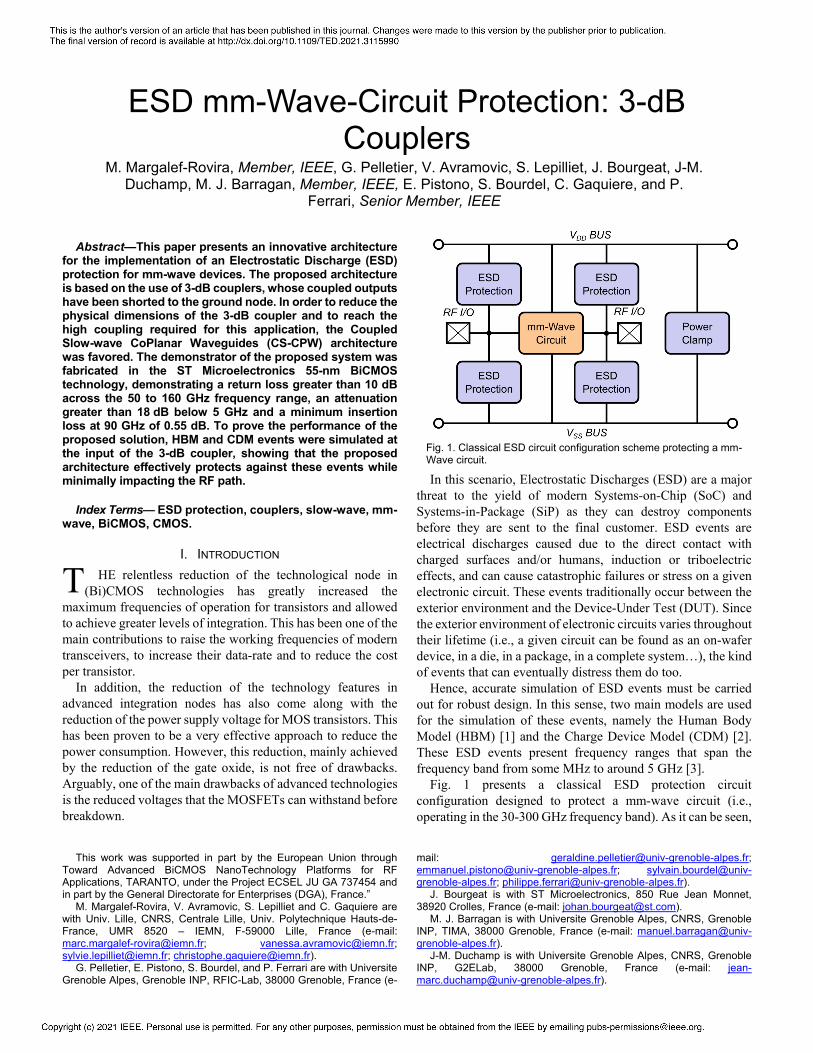
In this scenario, Electrostatic Discharges (ESD) are a major threat to the yield of modern Systems-on-Chip (SoC) and Systems-in-Package (SiP) as they can destroy components before they are sent to the final customer. ESD events are electrical discharges caused due to the direct contact with charged surfaces and/or humans, induction or triboelectric effects, and can cause catastrophic failures or stress on a given electronic circuit. These events traditionally occur between the exterior environment and the Device-Under Test (DUT). Since the exterior environment of electronic circuits varies throughout their lifetime (i.e., a given circuit can be found as an on-wafer device, in a die, in a package, in a complete system…), the kind of events that can eventually distress them do too. Hence, accurate simulation of ESD events must be carried out for robust design. In this sense, two main models are used for the simulation of these events, namely the Human Body Model (HBM) [1] and the Charge Device Model (CDM) [2]. These ESD events present frequency ranges that span the frequency band from some MHz to around 5 GHz [3]. Fig. 1 presents a classical ESD protection circuit configuration designed to protect a mm-wave circuit (i.e., operating in the 30-300 GHz frequency band). As it can be seen,
mail: [email protected]; [email protected]; [email protected]; [email protected]).
J. Bourgeat is with ST Microelectronics, 850 Rue Jean Monnet, 38920 Crolles, France (e-mail: [email protected]).
M. J. Barragan is with Universite Grenoble Alpes, CNRS, Grenoble INP, TIMA, 38000 Grenoble, France (e-mail: [email protected]).
J-M. Duchamp is with Universite Grenoble Alpes, CNRS, Grenoble INP, G2ELab, 38000 Grenoble, France (e-mail: [email protected]).
M. Margalef-Rovira, Member, IEEE, G. Pelletier, V. Avramovic, S. Lepilliet, J. Bourgeat, J-M. Duchamp, M. J. Barragan, Member, IEEE, E. Pistono, S. Bourdel, C. Gaquiere, and P.
Ferrari, Senior Member, IEEE
ESD mm-Wave-Circuit Protection: 3-dB Couplers
T
Fig. 1. Classical ESD circuit configuration scheme protecting a mm-Wave circuit.

M. Margalef-Rovira et al.: ESD mm-Wave-Circuit Protection : 3-dB Couplers 2
the ESD protections are placed in a shunt configuration. This approach is usually favored, as placing the protections in a series configuration, as shown in Fig. 2, requires time-consuming co-design strategies and usually presents unacceptable insertion loss. Hence, in such a configuration, the ESD protections must ideally present a null impedance to the ESD event while presenting an infinite impedance at the working frequency of the mm-wave circuit. However, ESD circuity, as any other electronic device, presents parasitic effects. In particular, capacitive effects tend to be predominant since diode-based protections are usually favored. Knowing that the protection that these ESD circuits is directly related to their size, and thus their parasitic capacitance, the well-known expression of the impedance of a capacitor (i.e., 𝑍𝑍𝑐𝑐𝑐𝑐𝑐𝑐𝑐𝑐𝑐𝑐𝑐𝑐𝑐𝑐𝑐𝑐𝑐𝑐 = −𝑗𝑗/(𝜔𝜔 ⋅ 𝐶𝐶), where 𝜔𝜔 and 𝐶𝐶 represent the angular frequency and the capacitance, respectively), makes it increasingly difficult to design ESD protections as the frequency increases. In this scenario, the design of circuits allowing to protect the mm-wave circuits and systems against ESDs while reducing their impact in the mm-wave design is a subject of major interest in the RF community. Several solutions have been studied in recent years [4]–[8]. Baluns have been cited [4], which allows relatively natural isolation, or the use of compensation circuits based either on an inductance or on a transmission line [5]–[8]. However, in all cases, the solutions proposed turn out to be narrow band, which obliges the designers to design protection for each considered frequency band.
In that context, this paper proposes an innovative architecture composed of a 3-dB coupler whose coupled ports have been connected to ground as a solution to protect mm-wave devices against ESD events. The proposed solution has the advantages of being broadband and presenting low insertion loss. This paper is organized as follows: section II describes the proposed architecture together with a theoretical analysis describing its principle of operation. Then, section III presents a practical realization of the proposed circuit in the ST Microelectronics 55-nm technology, and simulations showing the protection level against CDM and HBM ESD events. Finally, section IV discusses the main conclusions of this work.
II. PROPOSED ARCHITECTURE The proposed architecture differs from current designs of
ESD protections as it is a suitable approach for a wide variety of mm-wave circuits in terms of bandwidth. It is placed in a series configuration between the RF I/O and the RF input of the mm-wave circuit, as shown in Fig. 2.
As previously introduced, the proposed protection is composed of a 3-dB coupler whose coupled outputs have been connected to GND, creating a discharge path for the ESD event. In order to fully understand the working principle of this approach, let us consider a 3-dB coupler whose coupled ports are connected to an impedance 𝑍𝑍𝑙𝑙𝑐𝑐𝑐𝑐𝑙𝑙 that will ultimately be assimilated to an ideal short-circuit (i.e., 𝑍𝑍𝑙𝑙𝑐𝑐𝑐𝑐𝑙𝑙 = 0 Ω).
In integrated circuits two main topologies are used for the
implementation of 3-dB couplers (i) the branch line coupler and (ii) the coupled-line coupler [9]. It can be demonstrated that the performance of an ideal branch line coupler, in terms of coupling and phase imbalance, and return loss and isolation bandwidth, degrades faster as the operating frequency moves away from the operating frequency of the coupler. Hence, in order to obtain a more versatile solution in a broad range of frequencies, the coupled-line coupler architecture must be favored. Thus, this paper assumes that a coupled-line coupler is used. Nevertheless, the analysis carried out would also be valid at the operating frequency of a branch line coupler.
A. Principle of Operation Under these considerations, a wave analysis can be carried
out. For that purpose, let us analyze the 3-dB coupler depicted in Fig. 3, which is loaded at its coupled ports (i.e., ports II and III) by 𝑍𝑍𝑙𝑙𝑐𝑐𝑐𝑐𝑙𝑙. First, let us consider the general definition of the S-Parameters of a perfectly matched and isolated coupler to the 𝑍𝑍0 impedance:
𝑏𝑏1𝑏𝑏2𝑏𝑏3𝑏𝑏4
=
⎣⎢⎢⎡
0 𝑆𝑆𝐼𝐼𝐼𝐼,𝐼𝐼 𝑆𝑆𝐼𝐼𝐼𝐼𝐼𝐼,𝐼𝐼 0𝑆𝑆𝐼𝐼𝐼𝐼,𝐼𝐼 0 0 𝑆𝑆𝐼𝐼𝐼𝐼𝐼𝐼,𝐼𝐼𝑆𝑆𝐼𝐼𝐼𝐼𝐼𝐼,𝐼𝐼 0 0 𝑆𝑆𝐼𝐼𝐼𝐼,𝐼𝐼
0 𝑆𝑆𝐼𝐼𝐼𝐼𝐼𝐼,𝐼𝐼 𝑆𝑆𝐼𝐼𝐼𝐼,𝐼𝐼 0 ⎦⎥⎥⎤⋅
𝑎𝑎1𝑎𝑎2𝑎𝑎3𝑎𝑎4
(1)
where 𝑎𝑎𝑐𝑐 and 𝑏𝑏𝑐𝑐 represent the incident and reflected power waves of the coupler. In their turn, 𝑆𝑆𝐼𝐼,𝐽𝐽 represent the S-Parameters of the coupler. When the coupler is perfectly matched to 𝑍𝑍0, 𝑎𝑎4 presents a null value. Hence:
⎩⎨
⎧𝑏𝑏1 = 𝑆𝑆𝐼𝐼𝐼𝐼,𝐼𝐼 ⋅ 𝑎𝑎2 + 𝑆𝑆𝐼𝐼𝐼𝐼𝐼𝐼,𝐼𝐼 ⋅ 𝑎𝑎3𝑏𝑏2 = 𝑆𝑆𝐼𝐼𝐼𝐼,𝐼𝐼 ⋅ 𝑎𝑎1𝑏𝑏3 = 𝑆𝑆𝐼𝐼𝐼𝐼𝐼𝐼,𝐼𝐼 ⋅ 𝑎𝑎1𝑏𝑏4 = 𝑆𝑆𝐼𝐼𝐼𝐼𝐼𝐼,𝐼𝐼 ⋅ 𝑎𝑎2 + 𝑆𝑆𝐼𝐼𝐼𝐼,𝐼𝐼 ⋅ 𝑎𝑎3
(2)
Fig. 2. Coupler-based ESD protection circuit configuration scheme protecting a mm-Wave circuit.
Fig. 3. 3-dB coupler loaded by an impedance 𝒁𝒁𝒍𝒍𝒍𝒍𝒍𝒍𝒍𝒍 to its coupled ports (i.e., ports 2 and 3).
M. Margalef-Rovira et al.: ESD mm-Wave-Circuit Protection : 3-dB Couplers 3
Next, let us consider the reflection coefficient at the interface between 𝑍𝑍𝑙𝑙𝑐𝑐𝑐𝑐𝑙𝑙 and the coupled ports of the coupler. This reflection coefficient Γ𝐿𝐿 can be written as:
Γ𝐿𝐿 =𝑍𝑍𝑙𝑙𝑐𝑐𝑐𝑐𝑙𝑙 − 𝑍𝑍0𝑍𝑍𝑙𝑙𝑐𝑐𝑐𝑐𝑙𝑙 + 𝑍𝑍0
.
(3)
Hence:
𝑎𝑎2 = Γ𝐿𝐿 ⋅ 𝑏𝑏2
(4)
and:
𝑎𝑎3 = Γ𝐿𝐿 ⋅ 𝑏𝑏3.
(5)
Then, 𝑎𝑎2 and 𝑎𝑎3 in (2) can be substituted by (4) and (5), leading to:
⎩⎨
⎧𝑏𝑏1 = 𝑆𝑆𝐼𝐼𝐼𝐼,𝐼𝐼 ⋅ Γ𝐿𝐿 ⋅ 𝑏𝑏2 + 𝑆𝑆𝐼𝐼𝐼𝐼𝐼𝐼,𝐼𝐼 ⋅ Γ𝐿𝐿 ⋅ 𝑏𝑏3𝑏𝑏2 = 𝑆𝑆𝐼𝐼𝐼𝐼,𝐼𝐼 ⋅ 𝑎𝑎1𝑏𝑏3 = 𝑆𝑆𝐼𝐼𝐼𝐼𝐼𝐼,𝐼𝐼 ⋅ 𝑎𝑎1𝑏𝑏4 = 𝑆𝑆𝐼𝐼𝐼𝐼𝐼𝐼,𝐼𝐼 ⋅ Γ𝐿𝐿 ⋅ 𝑏𝑏2 + 𝑆𝑆𝐼𝐼𝐼𝐼,𝐼𝐼 ⋅ Γ𝐿𝐿 ⋅ 𝑏𝑏3
(6)
Substituting the expressions of 𝑏𝑏2 and 𝑏𝑏3 in (6) into the expressions of 𝑏𝑏1 and 𝑏𝑏4 in (6) yields:
𝑏𝑏1 = Γ𝐿𝐿𝑆𝑆𝐼𝐼𝐼𝐼,𝐼𝐼2 + 𝑆𝑆𝐼𝐼𝐼𝐼𝐼𝐼,𝐼𝐼2 𝑎𝑎1,
(7)
and
𝑏𝑏4 = 2Γ𝐿𝐿 ⋅ 𝑆𝑆𝐼𝐼𝐼𝐼,𝐼𝐼 ⋅ 𝑆𝑆𝐼𝐼𝐼𝐼𝐼𝐼,𝐼𝐼 ⋅ 𝑎𝑎1, (8)
Hence, 𝑆𝑆11, which represents the 𝑆𝑆𝐼𝐼,𝐼𝐼 of the coupler loaded by 𝑍𝑍𝑙𝑙𝑐𝑐𝑐𝑐𝑙𝑙, can be expressed as:
𝑆𝑆11 =𝑏𝑏1𝑎𝑎1
= Γ𝐿𝐿𝑆𝑆𝐼𝐼𝐼𝐼,𝐼𝐼2 + 𝑆𝑆𝐼𝐼𝐼𝐼𝐼𝐼,𝐼𝐼2 ,
(9)
and 𝑆𝑆21, which represents the 𝑆𝑆𝐼𝐼𝐼𝐼,𝐼𝐼 of the coupler loaded by 𝑍𝑍𝑙𝑙𝑐𝑐𝑐𝑐𝑙𝑙, as:
𝑆𝑆21 =𝑏𝑏4𝑎𝑎1
= 2Γ𝐿𝐿 ⋅ 𝑆𝑆𝐼𝐼𝐼𝐼,𝐼𝐼 ⋅ 𝑆𝑆𝐼𝐼𝐼𝐼𝐼𝐼,𝐼𝐼 . (10)
It can be demonstrated that the expression of 𝑆𝑆𝐼𝐼𝐼𝐼,𝐼𝐼 and 𝑆𝑆𝐼𝐼𝐼𝐼𝐼𝐼,𝐼𝐼 in a lossless, perfectly-matched coupler are [10]:
𝑆𝑆𝐼𝐼𝐼𝐼,𝐼𝐼 =𝑗𝑗𝑗𝑗 sin𝜃𝜃
√1 − 𝑗𝑗2 cos𝜃𝜃 + 𝑗𝑗 sin𝜃𝜃.
(11)
𝑆𝑆𝐼𝐼𝐼𝐼𝐼𝐼,𝐼𝐼 =√1 − 𝑗𝑗2
√1 − 𝑗𝑗2 cos𝜃𝜃 + 𝑗𝑗 sin𝜃𝜃.
(12)
where 𝜃𝜃 represents the electrical length of the coupler and 𝑗𝑗 the coupling coefficient, respectively. As the coupler is considered to present a 3-dB coupling coefficient, then 𝑗𝑗 = 1/√2.
Under these considerations, at the frequency for which the coupler presents 𝜃𝜃 = 𝜋𝜋/2 radians (i.e., the operating frequency of the coupler) 𝑆𝑆11 is null (because 𝑆𝑆𝐼𝐼𝐼𝐼,𝐼𝐼2 = −𝑆𝑆𝐼𝐼𝐼𝐼𝐼𝐼,𝐼𝐼2 ) and 𝑆𝑆21 =−𝑗𝑗 ⋅ Γ𝐿𝐿. Hence, if 𝑍𝑍𝑙𝑙𝑐𝑐𝑐𝑐𝑙𝑙 = 0 Ω, (i.e., a short-circuit) |𝑆𝑆21| = 1 This leads to a total transmission between port 1 and 4, and hence, ideally to a zero-loss transmission between the input and the isolated output of the coupler.
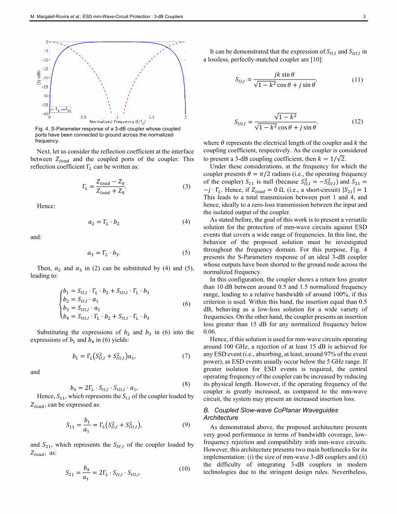
As stated before, the goal of this work is to present a versatile solution for the protection of mm-wave circuits against ESD events that covers a wide range of frequencies. In this line, the behavior of the proposed solution must be investigated throughout the frequency domain. For this purpose, Fig. 4 presents the S-Parameters response of an ideal 3-dB coupler whose outputs have been shorted to the ground node across the normalized frequency.
In this configuration, the coupler shows a return loss greater than 10 dB between around 0.5 and 1.5 normalized frequency range, leading to a relative bandwidth of around 100%, if this criterion is used. Within this band, the insertion equal than 0.5 dB, behaving as a low-loss solution for a wide variety of frequencies. On the other hand, the coupler presents an insertion loss greater than 15 dB for any normalized frequency below 0.06. Hence, if this solution is used for mm-wave circuits operating around 100 GHz, a rejection of at least 15 dB is achieved for any ESD event (i.e., absorbing, at least, around 97% of the event power), as ESD events usually occur below the 5 GHz range. If greater isolation for ESD events is required, the central operating frequency of the coupler can be increased by reducing its physical length. However, if the operating frequency of the coupler is greatly increased, as compared to the mm-wave circuit, the system may present an increased insertion loss.
B. Coupled Slow-wave CoPlanar Waveguides Architecture
As demonstrated above, the proposed architecture presents very good performance in terms of bandwidth coverage, low-frequency rejection and compatibility with mm-wave circuits. However, this architecture presents two main bottlenecks for its implementation: (i) the size of mm-wave 3-dB couplers and (ii) the difficulty of integrating 3-dB couplers in modern technologies due to the stringent design rules. Nevertheless,
Fig. 4. S-Parameter response of a 3-dB coupler whose coupled ports have been connected to ground across the normalized frequency.

M. Margalef-Rovira et al.: ESD mm-Wave-Circuit Protection : 3-dB Couplers 4
both of these issues can be dealt with by using the Coupled Slow-wave CoPlanar Waveguides (CS-CPW) architecture.
This architecture, shown in Fig. 5, was first presented in [11]. Then, a complete parametric model was proposed together with two demonstrators, showing the capabilities of this architecture [12]. Thanks to the slow-wave effect, firstly presented in [13] for CPWs, this architecture presents a reduced footprint, as compared to traditional coupled CPWs. The added floating shield produces the slow-wave effect, which allows the electrical coupling to be adjusted independently from the magnetic coupling. This independent adjustment enables higher coupling that would otherwise be difficult. High isolation is also achieved when the electric and magnetic coupling is equalized. These features make the CS-CPW architecture very suitable for the implementation of the proposed ESD protection.
III. EXPERIMENTAL RESULTS The demonstrator was designed and fabricated in the ST
Microelectronics BiCMOS 55-nm technology. This technology features an 8-metal Back-End-Of-Line (BEOL) with a thick upper metal. For this design, metals 7 and 8 were stacked using vias for the design of the signal and ground strips. The fingers were placed in the fifth metallic layer of the BEOL. The rest of the geometrical variables of the coupler were set to 𝑊𝑊𝑆𝑆 = 2 µm, , 𝑆𝑆 = 1.8 µm, 𝐺𝐺 = 20 µm, 𝑊𝑊𝐺𝐺 = 15 µm, 𝑆𝑆𝑆𝑆 = 𝑆𝑆𝑆𝑆 = 0.5 µm, a cut on the ribbon side, 𝐶𝐶𝑆𝑆, of 2 µm, respectively, for a total length of 255 µm. Ports 2 and 3 of the coupler were grounded using vias from the metal strips placed in metals 7 and 8 to the ground in metal 1 brought by the access lines that were designed using a microstrip topology. These dimensions led to an
effective footprint of 0.02 mm2. A microphotograph of the circuit is shown in Fig. 6.
A. S-Parameter Measurement The fabricated circuit was measured using two different
Vector Network Analyzers (VNAs): (i) a R&S ZVA67 with ZVA-Z110E extenders from 10 MHz to 110 GHz and (ii) a R&S ZVA24 with ZC220 extenders from 140 to 220 GHz. In order to set the measurement reference planes at the input of the DUT, an on-wafer Thru-Reflect-Line (TRL) calibration was performed [14]. For this purpose, two Line standards were used, a first Line with 315 µm of additional length, as compared to the Through standard, and a second Line presenting 150 µm of additional length.
The first Line was used for the lower frequency band as it showed an additional 90 degrees of phase shift around 110 GHz. The second band was calibrated using the Line standard that presented 315 µm of additional length, since it presented 90 degrees of additional phase shift at around 220 GHz. Fig. 6 shows a microphotograph of the fabricated device and the reference planes after the on-wafer calibration.
The circuit was subsequently measured under this setup. The measurement results are shown in Fig. 7 together with a 3D electromagnetic simulation carried out with ANSYS HFSS. Simulation and measurement results show good agreement. Some divergence is observed at the end of the measured band. This can probably be explained by the addition of dummy metals beneath the 3-dB coupler, needed to meet the density rules of the technology, which could not be simulated due to the computational requirements that this would represent.
If the bandwidth is defined as those frequencies showing a return loss greater than 10 dB, this device shows a bandwidth spanning from around 50 GHz to 160 GHz. Hence, if the central frequency of the device is considered to be placed at the median between those frequencies (i.e., 105 GHz), the system shows a relative bandwidth greater than 100%, as predicted by the theoretical study carried out in the previous section.
On the other hand, within this large frequency band, the system shows an insertion loss with a relatively low magnitude variation, ranging from a minimum of 0.55 dB, at around 90 GHz, to a maximum of 2 dB at 160 GHz.
Concerning the signal rejection at low frequencies, the system shows an insertion loss greater than 18 dB for frequencies below 5 GHz, leading to an efficient protection for ESD events, as shown in the next section.
Fig. 6. Microphotograph of the fabricated circuit and the reference planes after the on-wafer TRL calibration.
Fig. 7. Measured (solid line) and simulated (dashed line) S-Parameter response of the proposed structure.
Fig. 5. CS-CPW layout and its geometrical magnitudes.

M. Margalef-Rovira et al.: ESD mm-Wave-Circuit Protection : 3-dB Couplers 5
B. ESD Protection In the previous sections, the promising behavior of the
proposed circuit was shown. However, an accurate analysis of its performance against ESD events must be carefully studied. For this purpose, HBM and CDM events were simulated using the measured data shown in Fig. 7. 1) HBM event
Firstly, the former was studied using the setup shown in Fig. 8. To generate this event, a 100-pF capacitor is loaded with a voltage of 2 kV that is released through a series RL network (i.e., with an inductor of 7.2 µH and a resistor of 1.5 kΩ) and a 10-kΩ resistor placed in a parallel configuration to the DUT [1]. This configuration leads to a discharge with a time constant 𝜏𝜏 of 110 ns.
Using this setup, the time domain behavior of the signal injected by the circuit in Fig. 8 is studied up to 50 ns (i.e., around 𝜏𝜏/2), where the most critical part of the discharge occurs. In this time domain span, a peak current of 1.2 A is reached at around 15 ns at the input of the 3-dB coupler. A useful ESD protection against HBM events ensures that, ideally, none of this input current is transmitted to the fragile RF circuitry. Fig. 9 displays the ouptut current when this kind of event occurs. Note that a reduced – with a peak value of 2 mA – current is drawn by the event. As it can be seen, most of the current is dissipated in the via placed in the Thru port (i.e., port 3 in Fig. 3). To further investigate the protection offerred by the architecture proposed hereby, the voltages across it were also studied. These voltages are shown in Fig. 10. Note that, at the output of the protection circuit, a peak voltage with a reduced magnitude of 0.1 V is observed at around 15 ns. Hence, we can conclude that the proposed ESD protection circuit effectively protects against HBM-type events. 2) CDM event
The architecture proposed hereby can practically be considered as a global solution against ESD events if it protects against the other most common electrostatic discharge, the CDM event. This event presents rising times in the order of
300 ps, and hence shows a response shifted to greater frequencies, as compared to HBM events.
As seen in Fig. 7, in the frequency band where ESD events occur, the insertion loss of the coupler reduces as frequency increases. Hence, it is expected that the proposed protection behaves worse for CDM events than for HBM ones.
To analyze the effect of CDM discharges, a simulation bench was designed. The design of this CDM ESD synthesizer is cumbersome and out of the scope of this paper. The interested reader can find further information in [2].
In our analysis, the CDM event was generated to reach 5 A (i.e., an extreme case of these events at 350 V CDM). This configuration yielded, at the input of the protection circuit, to the current shown in Fig. 11. The time constant 𝜏𝜏 in the rising edge of the event’s current is equal to 170 ps.
CDM discharges usually damage circuits by generating a high-voltage at the input of the RF circuitry. Hence, to analyze the protection offered by the grounded 3-dB coupler the voltage at the output of the coupler must be studied.
Fig. 8. Used circuit to generate an HBM event.
Fig. 9. Currents at the different ports of the protection circuit under a HBM event. The input and output currents were obtained using the measured S-Parameters while the currents at the Thru and Coupled ports were obtained using the S-Parameters obtained using the EM simulation.
Fig. 10. Voltages across the proposed ESD protection under a HBM event.
Fig. 11. Current at the input of the protection circuit under a CDM event.
Fig. 12. Voltages across the proposed ESD protection under a CDM event.

M. Margalef-Rovira et al.: ESD mm-Wave-Circuit Protection : 3-dB Couplers 6
Fig. 12 presents the voltages at the different nodes of the 3-dB coupler during a CDM event. The proposed solution effectively reduces the voltage at the output of the protection circuit, which reaches a maximum of 4.3 V at 150 ps. This peak value represents a reduction of around 55% as compared to the voltage of the CDM event. In addition, note that the voltage decreases rapidly with time (i.e., the power of the ESD event is rapidly dissipated). As for the HBM event, most of the current is dissipated in the Thru port of the coupler due to its reduced electrical length at the frequencies at which the ESD events occur.
In a practical application, this voltage does not present a threat for most technological nodes, as the one used hereby. However, the most advanced technological nodes may still be sensitive to this voltage level. Nevertheless, as most of the ESD event energy is evacuated by the proposed solution, a small secondary CDM protection [15] would present a sufficient degree of robustness to ensure a proper protection. In this scenario, given that the physical size of the additional protection is considerably reduced, when compared to a classical protection, its parasitic capacitance would too.
To put the presented results into perspective, Table I presents a comparison with the current state-of-the-art literature. As introduced previously, the proposed approach qualifies as a suitable protection for HBM and CDM events while presenting the minimum insertion loss among the cited works and a reduced footprint. In addition, the proposed approach presents the largest bandwidth among the considered works.
TABLE 1 COMPARISON TO THE STATE-OF-THE-ART
Ref. Tech. Freq. (GHz)
|𝑆𝑆21| (dB)†
HBM Level (kV)
CDM Level (kV)
Area (mm2)
[4] 0.13-µm BiCMOS 90 -2.9 N/A N/A 0.03
[5] ‡ 65-nm CMOS 60 -1 2.5 N/A 0.027
[6] 65-nm CMOS 60 -2 2 N/A N/A
[7] 65-nm CMOS 77 -0.9 4.05 N/A 0.01
[8] 65-nm CMOS 60 -1.6 2.25 N/A 0.015
This work
55-nm BiCMOS 90 -0.55 2 0.35 0.02
†At central frequency. ‡Simulation-based results.
IV. CONCLUSIONS This paper has presented an innovative architecture for the
integration of broadband ESD protections for mm-wave circuits. The proposed architecture is composed of a 3-dB coupler, whose coupled outputs have been connected to the ground node. This architecture can be placed in the path of the RF signal with a relatively low impact to the protected mm-wave circuit.
The CS-CPW architecture was proposed for the integration of the 3-dB coupler as it leads to a reduced footprint while increasing the performance of the coupler.
A demonstrator was fabricated in the ST Microelectronics 55-nm BiCMOS technology and experimental results were reported hereby. The integrated device requires a surface of 0.02 mm2 for its integration. The protection reported a return
loss greater than 10 dB within the 50 GHz to 160 GHz band while only reporting 0.55-2 dB of insertion loss within this band. On the other hand, the rejection of the proposed system is greater than 18 dB for frequencies below 5 GHz and greater than 30 dB for frequencies below 1.2 GHz.
A detailed analysis of the performance of the proposed solution against HBM and CDM events was also carried out based on the measurement results of the protection circuit. This analysis shows that the proposed solution presents an alternative approach to protect mm-wave circuits against HBM and CDM events while minimally perturbing the RF path. In the case of CDM events, an additional protection may be required to protect the most advanced nanometric nodes. However, the approach proposed hereby drastically reduces the requirements of such ESD protections.
In addition, the rejection to the ESD events can be easily tuned by changing the electrical length of the 3-dB coupler with a minimal impact on the insertion loss of the ESD protection, thanks to the reduced magnitude variation shown in the 50-160 GHz frequency band.
REFERENCES [1] “ANSI/ESDA/JEDEC JS-001-2017 Human Body Model (HBM) Testing
of Integrated Circuits,” 2017. [2] “ANSI/ESDA/JEDEC JS-002-2018 - Charged Device Model (CDM) -
Device Level,” 2018. [3] S. H. Voldman, “ESD Design Synthesis,” in Esd, John Wiley & Sons, Ltd,
2011, pp. 1–51. [4] A. Mariano, B. Leite, T. Taris, and J. B. Bégueret, “Co-design of a
wideband double-balanced active mixer and transformer-based baluns for 77 GHz radar applications,” Microelectronics J., vol. 45, no. 11, pp. 1566–1574, 2014, doi: 10.1016/j.mejo.2014.09.008.
[5] M. H. Tsai and S. S. H. Hsu, “ESD protection design for microwave/millimeter wave low-noise amplifiers,” in 2014 IEEE International Wireless Symposium, IWS 2014, 2014, pp. 1–4, doi: 10.1109/IEEE-IWS.2014.6864242.
[6] L.-W. Chu et al., “Compact and low-loss ESD protection design for V-band RF applications in a 65-nm CMOS technology,” in 2012 IEEE International Symposium on Circuits and Systems (ISCAS), 2012, pp. 2127–2130, doi: 10.1109/ISCAS.2012.6271706.
[7] R. Berenguer, G. Liu, and Y. Xu, “A Low Power 77 GHz Low Noise Amplifier With an Area Efficient RF-ESD Protection in 65 nm CMOS,” IEEE Microw. Wirel. Components Lett., vol. 20, no. 12, pp. 678–680, 2010, doi: 10.1109/LMWC.2010.2087015.
[8] C.-Y. Lin et al., “ESD protection structure with inductor-triggered SCR for RF applications in 65-nm CMOS process,” in 2012 IEEE International Reliability Physics Symposium (IRPS), 2012, p. EL.3.1-EL.3.5, doi: 10.1109/IRPS.2012.6241893.
[9] D. M. Pozar, Microwave engineering, vol. 8, no. 2. John Wiley & Sons, 1989.
[10] R. K. Mongia, J. Hong, P. Bhartia, and I. J. Bahl, RF and microwave coupled-line circuits. Artech house, 2007.
[11] J. Lugo-Alvarez, A. Bautista, F. Podevin, and P. Ferrari, “High-directivity compact slow-wave CoPlanar waveguide couplers for millimeter-wave applications,” in European Microwave Week 2014: Connecting the Future, EuMW 2014 - Conference Proceedings; EuMC 2014: 44th European Microwave Conference, 2014, pp. 1072–1075, doi: 10.1109/EuMC.2014.6986624.
[12] M. Margalef-Rovira et al., “Design of mm-Wave Slow-Wave-Coupled Coplanar Waveguides,” IEEE Trans. Microw. Theory Tech., vol. 68, no. 12, pp. 5014–5028, 2020, doi: 10.1109/TMTT.2020.3015974.
[13] T. S. D. Cheung et al., “On-chip interconnect for mm-wave applications using an all-copper technology and wavelength reduction,” in Digest of Technical Papers - IEEE International Solid-State Circuits Conference, 2003, pp. 396–501 vol.1, doi: 10.1109/isscc.2003.1234353.
[14] G. F. Engen and C. A. Hoer, “Thru-Reflect-Line: An Improved Technique for Calibrating the Dual Six-Port Automatic Network Analyzer,” IEEE Trans. Microw. Theory Tech., vol. 27, no. 12, pp. 987–993, 1979, doi:

M. Margalef-Rovira et al.: ESD mm-Wave-Circuit Protection : 3-dB Couplers 7
10.1109/TMTT.1979.1129778. [15] Y. Morishita et al., “An investigation of input protection for CDM
robustness in 40nm CMOS technology,” in 2009 31st EOS/ESD Symposium, 2009, pp. 1–6.