esf eurocores programme fundamentals of...
TRANSCRIPT

ESF EUROCORES Programme
Fundamentals of NanoElectronics (FoNE)Highlights

European Science Foundation (ESF)
The European Science Foundation (ESF) is an independent, non-governmental organisation, the members of which are 78 national funding agencies, research performing agencies, academies and learned societies from 30 countries. The strength of ESF lies in its influential membership and in its ability to bring together the different domains of European science in order to meet the challenges of the future. Since its establishment in 1974, ESF, which has its headquarters in Strasbourg with offices in Brussels and Ostend, has assembled a host of organisations that span all disciplines of science, to create a common platform for cross-border cooperation in Europe. ESF is dedicated to promoting collaboration in scientific research, funding of research and science policy across Europe. Through its activities and instruments ESF has made major contributions to science in a global context. ESF covers the following scientific domains:
• Humanities• Life, Earth and Environmental Sciences• Medical Sciences• Physical and Engineering Sciences• Social Sciences• Marine Sciences • Materials Science and Engineering• Nuclear Physics• Polar Sciences• Radio Astronomy
• Space Sciences
www.esf.org
Cover Image: Artistic view of the image-potential states above a cobalt island on a gold surface. Courtesy of Professor Chris Van Haesendonck
Physical and Engineering Sciences (PESC)
The Physical and Engineering Sciences are key drivers for research and innovation, providing fundamental insights and creating new applications for mankind.The goal of the ESF Standing Committee for Physical and Engineering Sciences (PESC) is to become the pan-European platform for innovative research and competitive new ideas while addressing societal issues in a more effective and sustainable manner. The Committee is a unique cross-disciplinary group, with networking activities comprising a good mix of experimental and theoretical approaches. It distinguishes itself by focusing on fundamental research and engineering. PESC covers the following broad spectrum of fields: chemistry, mathematics, informatics and the computer sciences, physics, fundamental engineering sciences and materials sciences.
Editorial Board• Professor Vladimir Falko, Project Leader,
Lancaster University, Lancaster, United Kingdom• Professor Giuseppe Iannaccone, Project Leader,
IEIIT-CNR sezione di Pisa, Pisa, Italy• Professor Andrew Briggs, Project Leader,
Oxford University, Oxford, United Kingdom• Dr Christopher Marrows, Project Leader,
University of Leeds, Leeds, United Kingdom• Professor Bogdan Bulka, Project Leader,
Polish Academy of Sciences, Poznan, Poland• Mr Neil Williams, PESC Head of Unit, ESF, France• Dr Ana Helman, EUROCORES Programme
Coordinator, ESF, France• Dr Isabel Van De Keere, Junior Science Officer –
EUROCORES, ESF, France• Dr Hilary J. Crichton, Junior Science Officer –
EUROCORES, ESF, France• Ms Catherine Lobstein, EUROCORES Administrator,
ESF, France

Contents
Foreword 3
1. Governing Bodies 5
1.1 Management Committee 5
1.2 Scientific Committee 5
1.3 International Review Panel 5
1.4 Funding Organisations 6
1.5 Support Team at the ESF 7
2. Description of the FoNE Programme 9
2.1 Rationale and Objectives 9
2.2 Scientific Themes and Research Objectives of the Call for Proposals 9
2.3 List of Projects 11
2.4 EUROCORES Selection Process 12
2.5 EUROCORES Acknowledgements 13
3. Highlights of the FoNE Collaborative Research Projects (CRPs) 15
3.1 Spin-Coherent Transport and Control in Quantum Nanostructures (SpiCo) 15
3.2 Device Electronics Based on Nanowires and Nanotubes (DEWINT) 17
3.3 Intra-Molecular Propagation of Electron Spin States (IMPRESS) 19
3.4 Domain Walls and Spin-Polarised Currents (SPINCURRENT) 21
3.5 Spin-dependent Transport and Electronic Correlations in Nanostructures (SPINTRA) 23
4. Networking and Dissemination Activities 27
5. Outreach Activities 33
6. Related ESF Activities 35
6.1 Research Networking Programmes 35
6.2 EUROCORES Programme: EuroGRAPHENE 37
Annex: FoNE Review Panel Consensus Report 39


Fun
dam
enta
ls o
f N
an
oEle
ctro
nic
s (F
oNE)
3FoNE was one of the early EUROCORES pro-grammes that were launched in 2005, recognising the need for basic research on nanoelectronics in Europe. The goal of FoNE was to generate funda-mental knowledge within the field of nanoscale electronics and to create a synergy between the activities of world-leading, European research groups through real scientific collaborations and networking activities.
Over the course of the past three years, signifi-cant scientific achievements have been made by the synergistic efforts of five Collaborative Research Projects, resulting in the development of common tools and producing many high-level publications. Several advances were made in the field: the realisa-tion of fullerenes functionalised with spin chains encapsulated in carbon nanotubes (peapods) and measurement of the spin properties; demonstra-tion of a frequency-dependent spin torque resonator based on current-threshold magnetic domain-wall pinning physics; creation of a quantum resistance standard using graphene on silicon carbide; creation of a non-magnetic spin-photovoltaic polarimeter that provides a direct electrical measurement of light polarisation.
Through its successful conference series and joint workshops, FoNE fostered innovative and multidisciplinary collaborations among the pro-ject investigators and their laboratories. New project ideas were developed, tools and know-how exchanged, and young postdoctoral and PhD stu-dents had the opportunity to present their research to leaders in the field.
The aim of this report is to illustrate the high-lights in terms of scientific results, and networking and dissemination activities during the duration of the programme. The collaborations that have started will hopefully continue and strengthen in order to contribute to the international endeavour to address the many remaining questions and chal-lenges in this exciting field.
With this I would like to thank the five Project Leaders and all scientists and ESF colleagues involved for their high-level contribution and com-mitment.
Mr Neil WilliamsHead of UnitPhysical and Engineering Sciences Unit (PESC)
Forewordl l l


Fun
dam
enta
ls o
f N
an
oEle
ctro
nic
s (F
oNE)
5
1.Governing Bodiesl l l
1.1 Management Committee Mrs Karolina BonkovaCzech Science Foundation, Czech Republic
Dr Paul BurkhardSwiss National Science Foundation, Natural and Engineering Sciences, Division Mathematics, Switzerland
Dr Anna D’AmatoConsiglio Nazionale delle Ricerche,National Research Council, Dipartimento per le Attivita’ Internazionali Servizio I Roma, Italy
Dr Severino Falcón MoralesMinisterio de Ciencia e Innovación, Subdirección General de Programas Europeos, Dirección General de Cooperación Internacional, Spain
Dr Benno HinnekintFonds voor Wetenschappelijk Onderzoek – Vlaanderen, Belgium
Dr Jaroslav HorvatInstitut Ruder Boskovic, Croatia
Professor Jeno KürtiEötvös Loránd University, Department of Biological Physics, Hungary
Professor Stefan LubySlovak Academy of Sciences, Slovak Republic
Ms Constantina MakriResearch Promotion Foundation, European Research Programmes and International Cooperation Unit, Cyprus
Professor Ivan NedkovBulgarian Academy of Sciences, Institute of Electronics, Bulgaria
Dr Doris RakoczyFonds zur Förderung der Wissenschaftlichen Forschung, Austria
Professor Jozef SpalekMarian Smoluchowski Institute of Physics, Jagiellonian University, Faculty of Physics, Astronomy and Applied Computer Science, Department Condensed Matter Theory, Poland
Professor Sigitas TamuleviciusKaunas University of Technology, Institute of Physical Electronics, Department of Optical Technologies, Lithuania
Ms Rita WardEnterprise Ireland, International Technology Programmes, Ireland
Dr Jonathan WilliamsEngineering and Physical Sciences Research Council, United Kingdom
1.2 Scientific CommitteeProfessor Andrew Briggs (IMPRESS)University of Oxford, Department of Materials, United Kingdom
Professor Bogdan Bulka (SPINTRA)Institute of Molecular Physics, Polish Academy of Sciences, Poznan, Poland
Professor Vladimir Falko (SpiCo)Physics Department, Lancaster University, United Kingdom
Professor Giuseppe Iannaccone (DEWINT)IEIIT-CNR sezione di Pisa, c/o Dipartimento di Ingegneria dell’Informazione, Pisa, Italy
Dr Christopher Marrows (SPINCURRENT)University of Leeds, Faculty of Mathematics and Physical Sciences, United Kingdom
1.3 International Review PanelProfessor Renato BozioDepartment of Chemical Sciences, University of Padova, Italy
Professor Yvan BruynseraedeLaboratorium voor Vaste-Stoffysica en Magnetisme, K.U. Leuven, Belgium
Dr Arvaidas GaldikasPhysics Department, Kaunas University of Technology, Lithuania
Fun
dam
enta
ls o
f N
an
oEle
ctro
nic
s (F
oNE)
6
Professor Mieczyslaw JalochowskyInstitute of Physics, Marie Curie-Slodowska University, Poland
Professor John H. JeffersonQinetiQ Malvern, Sensors and Electronic Division, United Kingdom
Professor Georgy MladenovBulgarian Academy of Sciences, Institute of Electronics, Bulgaria
Professor Joan Ramòn MoranteDepartament d‘Electrònica, Facultat de Física, Universitat de Barcelona, Spain
Professor Martyn E. PembleAdvanced Materials and Surfaces Group, Tyndall National Institute, University College Cork, Ireland
Dr Marc SanquerCommissariat à l’Énergie Atomique/Direction des Sciences de la Matière (CEA), DRFMC/SPSMS, France
Professor Wolf-Dieter SchneiderLPS - IPN - SB - EPF, Laboratoire de Physique des Surfaces, Université de Lausanne, Switzerland
Dr Ludvik SmrckaInstitute of Physics, ASCR, Czech Republic
Professor Mark TuominenDepartment of Physics, 411 Hasbrouck Laboratory, University of Massachusetts, United States
Dr Milan TyslerInstitute of Measurement Science, SAS, Slovak Republic
Professor Tamas UngarDepartment of General Physics, Eötvös Lorand University, Hungary
Professor Magnus WillanderPhysical Electronics and Photonics, Department of Physics, Chalmers University of Technology and Gothenburg University, Sweden
1.4 Funding Organisations (actual funding received from organisations marked with *)
Austria: Fonds zur Förderung der Wissenschaftlichen Forschung *
Belgium: Fonds voor Wetenschappelijk Onderzoek - Vlaanderen *
Bulgaria: Bulgarian Academy of Sciences
Croatia: Croatian Academy of Sciences and Arts
Cyprus: Cyprus Research Promotion Foundation
Czech Republic: Czech Science Foundation*
France: Commissariat à l’Énergie Atomique/Direction des Sciences de la Matière*
Hungary: Hungarian Academy of Sciences
Ireland: Enterprise Ireland*
Fun
dam
enta
ls o
f N
an
oEle
ctro
nic
s (F
oNE)
7
Italy: National Research Council*
Lithuania: Lithuanian State Science and Studies Foundation
Poland: Polish Academy of Sciences*
Slovak Republic: Slovak Academy of Sciences
Spain: Interministerial Committee on Science and Technology*
Switzerland: Swiss National Science Foundation*
United Kingdom: Engineering and Physical Sciences Research Council*
1.5 Support Team at the ESF
Physical and Engineering Sciences UnitMr Neil Williams: Head of the PESC Unit (2009-11)Dr Patrick Bressler: Head of the PESC Unit (2004-09)
Dr Ana Helman: EUROCORES Coordinator (2008-11)Dr Isabel Van De Keere: Junior Science Offi cer – EUROCORES (2010)Dr Hilary J. Crichton: Junior Science Offi cer – EUROCORES (2011)Dr Antonella Di Trapani: EUROCORES Coordinator (2005-08)Dr Josefa Limeres: EUROCORES Coordinator (2004-05)Ms Catherine Lobstein: EUROCORES Administrator (2004-11)
Chief Executive Offi ceDr Farzam Ranjbaran: EUROCORES Scheme Coordinator (2008-11)Dr Svenje Mehlert: EUROCORES Scheme Coordinator (2004-08)Ms Päivi McIntosh: EUROCORES Scheme Administrator (2010)Ms Eléonore Piémont: EUROCORES Scheme Administrator (2009-11)Ms Stephanie Pery: EUROCORES Scheme Administrator (2006-2008)
CommunicationMs Sabine Schott: Publications Offi cerDr Michiko Hama: Communications Offi cer
Finance Mr David Weber: Director of Finance and AdministrationMs Philippa Rowe: Finance Controller

Fun
dam
enta
ls o
f N
an
oEle
ctro
nic
s (F
oNE)
9
2. Description of the FoNE Programmel l l
2.1 Rationale and Objectives
The main motivation to launch the FoNE pro-gramme came from the need to enhance the basic understanding of physical phenomena in nanoscale devices and therefore create the necessary knowl-edge for a society in which microelectronics is gradually replaced by nanoelectronics.
FoNE was a three-year research programme, which recognised that a comprehensive understand-ing of the above phenomena is crucial to the future development of nanoscale electronics. It aimed to accelerate the pace of European research by concen-trating the activities of and facilitating networking between world-leading, European research groups.
The goal was to bring together the hitherto distinct fields of nanoscale physics, magnetism, superconductivity and molecular electronics, and explore a range of new physical phenomena involving quantum dots, quantum wires, carbon nanotubes and molecular point contacts. Many of these share generic properties arising from the pres-ence of phase-coherent dynamics and correlations. By studying these phenomena in different contexts, FoNE provided a forum for the cross-fertilisation of techniques and the exploration of emerging fields such as graphene.
2.2 Scientific Themes and Research Objectives of the Call for Proposals
The text below summarises the scientific objectives and research topics as stated in the FoNE Call for proposals issued in 2004.
To realise the immense potential of nanoscale electronics, it is necessary to understand and con-
trol size, interface scattering and proximity effects in a wide variety of hybrid nanostructures. At a fundamental level, proximity effects in hybrid nano-structures, such as ferromagnetic superconducting point contacts, arise from the interplay between cor-related systems with different broken symmetries. At a practical level they lead to new and unexpected device and sensor capabilities. When contacting a single molecule to a metallic reservoir, the physics of the contact can dominate transport characteristics of the resulting hybrid structure. Therefore stud-ies of the interplay between conventional metallic transport and the level structure of isolated mol-ecules are crucial. Single molecules are also a means of communicating electron correlations from one contact to another and therefore provide a new opportunity for discovering novel proximity effects.
The ongoing miniaturisation of electronic devices and sensors also brings nanomechanical degrees of freedom into play, because mechanical and electri-cal degrees of freedom as a rule are strongly coupled on this scale. Nanoelectromechanical phenomena will therefore be important for future materials and devices. Similarly current-induced magneti-sation reversal also poses a major challenge to our fundamental understanding of electronics proper-ties of ferromagnets. This phenomenon might be used as a mechanism for writing information in magnetic random access memories. The poten-tial of nano-spintronics and hybrid devices with integrated superconducting, semiconducting and magnetic functionalities is only just beginning to be explored, but will surely impact on coming technologies on a ten-year timescale. Unlike their metallic counterparts, ferromagnetic semicon-ductors represent a new and relatively unexplored field of materials and basic physics research.
Fun
dam
enta
ls o
f N
an
oEle
ctro
nic
s (F
oNE)
10
Ferromagnetic-semiconductor nanostructures are also of fundamental importance for the understand-ing of collective magnetic phenomena in nanoscale solid-state systems and at the same time they add new degrees of freedom to future device designs.
The primary focus of the FoNE EUROCORES programme is on fundamental nanoscale phenom-ena affecting electron transport and can be naturally structured into four related topics:
Topic 1. Quantum transport, noise and correlations in quantum dots, wires and other novel structuresThe aim here is to generate new theoretical and experimental breakthroughs concerning the fun-damentals of electron transport in quantum wires and quantum dots based on semiconductor hetero-structures. Systems with non-zero electron density that are beyond the phenomenological Fermi liq-uid model, such as the Luttinger liquid, will also be considered.
Quantum shot noise in small mesoscopic or nanoscale systems is concerned with problems like quantum detectors where noise plays a central role. Areas of theoretical interest will include differ-ent approaches to counting statistics, the probing and manipulating of entangled states and prob-ing non-local coherence. Systems of interest are superconductor-normal systems, superconductor-ferromagnetic systems and quantum dots, along with noise signatures of systems with interactions (correlations), including Luttinger liquid carriers like carbon nanotubes. Experimental problems include the extension of present day measurement techniques to increase sensitivity and higher fre-quencies, and include challenges in the fabrication of samples, especially hybrid structures.
The ongoing miniaturisation of electronic devices and sensors brings new physics into play associated with nanoelectromechanical properties. This research topic will be a platform for examin-ing such effects, including the question of how the accuracy of nanoelectromechanical single-electron devices can be enhanced substantially compared to ordinary single-electron transistors.
Topic 2. Molecular-scale electronics and atomic contactsThis activity will investigate possibilities for using atoms or molecules as basic electronic building blocks. It was realised some time ago that organic molecules are very attractive for building electronic circuits in view of the rich variety of properties that can be introduced by use of chemical synthesis.
Rapid advances are now being made in the labora-tory and European laboratories need a coordinated activity in this area if they are to remain competi-tive.
Also included will be common experimental and theoretical investigations of the electronic and electromechanical properties of carbon nanotube hybrid structures. Carbon nanotubes represent a prominent class of molecular quantum wires, which exhibit a variety of unique features such as very unusual transport properties. Fundamental phys-ics (e.g. Luttinger liquid behaviour) as well as their potential as building blocks for future electronics on molecular scales will be investigated.
Topic 3. Nanoscale spin-dependent transport and controlThis topic will aim at optimising spin injection and detection, to find novel physics in the manipulation of spins, and to reach a more thorough understand-ing of spin-current induced magnetisation reversal in metals and semiconductors. Activities are likely to include:a. The interface properties of metals with oxides,
and both metals and oxides with semiconductors, in order to understand the process of electrical spin injection and detection and how these are best achieved.
b. Studies of the manipulation of spins in these structures by external fields and forces such as electric fields (through gated structures), mag-netic fields, currents and optical methods.
c. Studies of spin-current-induced magnetisation reversal, which has potential application particu-larly for magnetic random access memory.
d. Studies of nanoscale ferromagnetic semiconduc-tors.
Topic 4. Proximity effects and hybrid nanostructuresThe increasing possibilities afforded by modern nanoscale fabrication techniques now make it possi-ble to answer some major conceptual questions, long ago posed theoretically, regarding superconductor-ferromagnetic hybrid nanostructured devices. These concern the interaction of a Cooper pair with the exchange field of a ferromagnet, and the behaviour of (single) spins in a superconductor. The richness of the questions derives from the large parameter space of the problem, and the different issues in different corners. Spin polarisation, diffusion constants, mag-netic dipole fields, ferromagnetic domain walls, and electronic structure of the interfaces are all part of experimental reality, and it takes careful and well-

Fun
dam
enta
ls o
f N
an
oEle
ctro
nic
s (F
oNE)
11
controlled experiments to disentangle them.Studies are expected of NS and SNS junctions,
where N is either a very thin metal, or a nanotube, or a semiconductor and S is superconductor. A com-mon feature of these compounds is their low density of carriers, which could be modulated by field effect and is easily brought out of equilibrium. Moreover many of them (carbon nanotubes and 2- dimen-sional electron gases) exhibit a very high mobility. The study of such NS and SNS junctions is a prereq-uisite for developing systems and devices where the superconducting proximity effect is controlled by gates, where the ballistic nature of carriers is cru-cial or where coherent entangled Andreev pairs are manipulated.
Facts and Figures
Deadline for Applications: 15 May 2005
Funded Collaborative Research Projects (CRPs): 5, consisting of 25 Individual Research Projects in 10 different countries
Duration of the programme: November 2006 – March 2010
Budget for research: 4.9 M€
2.3 List of Projects
Spin-Coherent Transport and Control in Quantum Nanostructures (SpiCo)
Principal Investigators:
•Vladimir Falko (Project Leader) Lancaster University, IENS, Physics Department,
Lancaster, United Kingdom•Silvano De Franceschi Laboratorio Nazionale TASC, CNR-INFM,
Basovizza, Italy•Klaus Ensslin Eidgenössische Technische Hochschule
Hönggerberg, Laboratorium für Festkörperphysik, Zürich, Switzerland
•Tomas Jungwirth Academy of Sciences of the Czech Republic,
Institute of Physics, Department of Surface and Interfaces, Prague, Czech Republic
•Daniel Loss University of Basel, Department of Physics,
Basel, Switzerland
Device Electronics Based on Nanowires and Nanotubes (DEWINT)
Principal Investigators:
•Giuseppe Iannaccone (Project Leader) IEIIT-CNR sezione di Pisa, c/o Dipartimento di
Ingegneria dell Informazione, Pisa, Italy•Merlyne De Souza De Montfort University, Leicester,
United Kingdom and University of Sheffield, Department of
Electronic & Electrical Engineering, Sheffield, United Kingdom
•Hans Kosina Vienna University of Technology, Institute
for Microelectronics, Vienna, Austria•Bill Milne University of Cambridge, Department of
Engineering, Cambridge, United Kingdom
Intra-Molecular Propagation of Electron Spin States (IMPRESS)
Principal Investigators:
•Andrew Briggs (Project Leader) Oxford University, Division of Mathematics
and Physical Sciences, Department of Materials, Oxford, United Kingdom

Fun
dam
enta
ls o
f N
an
oEle
ctro
nic
s (F
oNE)
12
•Laszlo Forro École Polytechnique Fédérale de Lausanne,
Institute of Physics of Complex Matter, Lausanne, Switzerland
•Herwig Peterlik Universität Wien, Institut für Materialphysik,
Vienna, Austria
Domain Walls and Spin-Polarised Currents (SPINCURRENT)
Principal Investigators:
•Christopher Marrows (Project Leader) University of Leeds, Faculty of Mathematics
and Physical Sciences, School of Physics and Astronomy, Leeds, United Kingdom
•Rolf Allenspach IBM Research Division, Rüschlikon, Switzerland•Michael Coey Trinity College, School of Physics, Dublin,
Ireland•Vladimir Falko Lancaster University, IENS, Physics Department,
Lancaster, United Kingdom
Associated Partners:
•Michel Viret CEA Saclay, Gif-sur-Yvette, France •David Williams Hitachi Cambridge Laboratory, Cambridge,
United Kingdom
Collaborator:
•Dafiné Ravelosona Institut d’Électronique Fondamental,
Université de Paris Sud, Orsay, France
Spin-dependent Transport and Electronic Correlations in Nanostructures (SPINTRA)
Principal Investigators:
•Bogdan Bulka (Project Leader) Polish Academy of Sciences, Institute
of Molecular Physics, Poznan, Poland•Farkhad Aliev Universidad Autónoma de Madrid, Facultad
de Ciencias, Depto Fisica de la Materia Condensada, C III, Madrid, Spain
•Jozef Barnaś Adam Mickiewicz University, Department
of Physics, Poznan, Poland•Tomasz Dietl Polish Academy of Sciences, Institute of Physics
and College of Science, Warszawa, Poland
•Vit Novák Institute of Physics ASCR, Prague,
Czech Republic•Gunther Springholz Johannes Kepler Universität Linz, Institut für
Halbleiter- und Festkörperphysik, Linz, Austria •Arturo Tagliacozzo Universita’ di Napoli “Federico II” Facoltà
di Scienze, Dipartimento di Scienze Fisiche, Napoli, Italy
•Chris Van Haesendonck Katholieke Universiteit Leuven, Laboratory
of Solid-State Physics and Magnetism, Department of Physics, Leuven, Belgium
Associated Partners:
•Bryan Gallagher University of Nottingham, School of Physics
and Astronomy, Nottingham, United Kingdom•Joerg Wunderlich Hitachi Cambridge Laboratory, Cavendish
Laboratory, Cambridge, United Kingdom
2.4 EUROCORES Selection Process
2.4.1 Theme SelectionNew and challenging ideas for EUROCORES pro-grammes are invited from the scientific community through an annual Call for Theme Proposals. In addition to criteria including scientific quality, nov-elty and feasibility, the proposals are evaluated on the basis of the requirement for European collabora-tion: why it is necessary to conduct the programme at a European level and how will the programme strengthen and advance Europe’s scientific position in a global context. Each proposal is sent for written external assessment to at least three referees. Based on these reviews, the Science Advisory Board recom-mends which themes are to be further developed, a decision which is then ratified by the Governing Council.
2.4.2 Project SelectionThe peer review of the Collaborative Research Project (CRP) proposals in a EUROCORES programme like FoNE is a multi-stage process, including the establishment of an international and independent Review Panel. In response to an open Call for proposals, outline proposals of about three pages are submitted by a team of applicants (minimum three from three different countries). At that stage, the Review Panel is responsible for the sifting of outline proposals prior to the invitation
Fun
dam
enta
ls o
f N
an
oEle
ctro
nic
s (F
oNE)
13
of full proposals. At the full proposals stage, each proposal is sent for written external assessments to at least three referees, including referees from outside Europe. Applicants are given an opportu-nity to reply to the anonymous referee reports.
Written referees’ assessments and replies by applicants are then considered by the Review Panel with scientific quality being the main selection cri-terion. The Review Panel makes recommendations for funding of CRPs, with prioritisation, which ESF communicates to the EUROCORES Funding Organisations (EFOs).
After the international peer review process managed by the ESF, and the subsequent funding decisions by the EFOs, five CRPs were selected for FoNE and launched in 2006. These five CRPs con-sisted of 25 individual research projects based in 10 different European countries. In Chapter 3, the results of the five FoNE research teams’ work are highlighted with respect to both the programme aims and to the field of nanoelectronics and con-densed matter physics in general.
2.4.3 Management CommitteeAt the time that the Call for proposals is published, a Management Committee (MC) is established (see page 5 for the FoNE MC).•The MC has overall responsibility for the
EUROCORES programme within the guidelines of the EUROCORES Scheme;
•TheMC can request expert advice from theEUROCORES Scientific Committee, Review Panel or any other ad hoc advisory group;
•Members support the EUROCORES reviewprocess by nominating potential Review Panel members and external expert referees on behalf of their funding organisation;
•EachMCmemberisresponsibleforliaisingwiththeir funding organisation, including supervision of the funding process for EUROCORES projects within their organisation;
•Members may attend all meetings of theEUROCORES programme as observers.
2.4.4 Mid-Term and Final ReviewsEach EUROCORES programme undergoes two comprehensive reviews to evaluate its progress at the mid- and final stages. The aim is to assess scientific cooperation and interactions among the investiga-tors and provide recommendations for the future.
The assessment is carried out by remote evalua-tion where the project leaders are asked to report on the progress using the listed criteria:•Novelty/Originality:Mostinnovative/original
scientific contribution of each CRP to the pro-gramme and to the relevant field of research;
•MultidisciplinaryResearch:HowiseachCRPworking towards (or achieving) multidisciplinary research;
•CollaborativeResearch:Resultsobtainedwithinthe CRP during this reporting period that would not have been achieved (or would have taken longer to achieve) in an individual project;
•European-addedValue:Europeandimensiongiven to national funding (e.g., building up ERA; developing a critical mass of expertise; address-ing issues of scale and scope). For CRPs involving partners outside Europe: a clear example illustrat-ing their added value to the programme and their contribution to the relevant field of research in Europe;
•RelevancetotheCall:Achievementmostrelevantto the Call.
Based on these reports, the Review Panel is then asked to examine the scientific achievements; net-working, training and dissemination activities; and assess the overall potential of the programme.
FoNE had positive mid-term and final reviews by the Review Panel, who commented in the final report that ‘the five CRPs contributed significantly to progress in nanoscale electronics, with a sig-nificant number of publications, including in high impact journals. The major strength of the pro-gramme was in establishing collaborations in the various subfields within the nanoelectronics area, uniting laboratories from different countries and disciplines, leading to more publications and qual-ity high-profile studies’. The detailed report of the FoNE Review Panel is available in the Annex.
2.5 EUROCORES Acknowledgements
To promote the EUROCORES programme and the national funding organisations who support it (and prior to 2008, the European Commission), all publications, posters, websites and other dissemina-tion outputs are required to be clearly identified as being programme-funded or co-funded. This is an important indicator for monitoring the output of the programmes, particularly peer-reviewed pub-lications.
For FoNE, the acknowledgement until 2008 was:The European Science Foundation (ESF) provides scientific coordination and support for network-ing activities of funded scientists currently through

Fun
dam
enta
ls o
f N
an
oEle
ctro
nic
s (F
oNE)
14
the EC FP6 Programme, under contract no. ERAS-CT-2003-980409. Research funding is provided by participating organisations. FoNE is managed by the Physical and Engineering Sciences Committee (PESC) at the ESF.
From 2009 onwards the acknowledgement is:The aim of the European Collaborative Research (EUROCORES) Scheme is to enable researchers in different European countries to develop collaboration and scientific synergy in areas where European scale and scope are required to reach the critical mass neces-sary for top class science in a global context.
The scheme provides a flexible framework which allows national basic research funding and perform-ing organisations to join forces to support excellent European research in and across all scientific areas.
Until the end of 2008, scientif ic coordina-tion and networking was funded through the EC FP6 Programme, under contract no. ERAS-CT-2003-980409. As of 2009, the national funding organisations will provide the funding for the scientific coordination and networking in addition to the research funding.

Fun
dam
enta
ls o
f N
an
oEle
ctro
nic
s (F
oNE)
15
3. Highlights of the FoNE Collaborative Research Projects (CRPs)l l l
3.1 Spin-coherent Transport and Control in Quantum Nanostructures (SpiCo)
Principal Investigators
•Vladimir Falko (Project Leader)•SilvanoDeFranceschi•KlausEnsslin•TomasJungwirth•DanielLoss
Funding Organisations
•Czech Republic: Czech Science Foundation•Italy: National Research Council •Switzerland: Swiss National Science Foundation•United Kingdom: Engineering and Physical
Sciences Research Council
The SpiCo project aimed at performing a system-atic investigation of spin-related quantum transport phenomena in semiconductor wires and dots of new and recently developed materials in order to iden-tify the relevant physics underlying coherent spin transport and control in low-dimensional systems.
The objectives of the project were:– to investigate spin-dependent transport in mes-
oscale semiconductor structures with a view to designing methods of characterisation of spin-related parameters in new materials;
– to find materials and conditions suitable for incoherent and coherent transfer of spin in nano- and micro-cir-cuits and to develop methods to detect spin currents;
– to investigate fundamental aspects of electron spin dynamics in quantum dots and dot circuits, and mechanisms of spin relaxation and de-coher-ence, in order to identify materials and devices suitable for quantum information processing.
The main overlapping interests and complementary expertise of the participating researchers enabled quantum transport studies to be extended to new types of nanostructures, such as semiconductor nanowires; quantum dots embedded in nanowires; graphene-based devices and nanostructures; and magnetic semiconductors.
Research on quantum dots in the groups led by De Franceschi and Ensslin resulted in the observation of an electrically tuneable singlet-triplet degeneracy in an InGaAs/GaAs single quantum dot at zero mag-netic field. Theoretical studies on quantum dots included examining electron spins in InAs nanow-ire-based quantum dots placed inside a transmission line resonator by the group of Loss. Collaborative work between the research groups headed by Falko and Loss produced a theory for hyperfine interac-tion effects in quantum dots leading to nuclear spin polarisation control and polarisation bistability in optically pumped quantum dots.
De Franceschi’s group performed an experimen-tal study of the quantum transport phenomena in InAs and InP nanowires connected to superconduct-ing electrodes. The behaviour was seen to depend on the tunnel coupling strength between the nanowire and superconductor: Coulomb blockade dominates when the coupling is weak whereas for strong cou-pling the transport is governed by Andreev reflection. They were also the first to study low-temperature transport in p-type GaAs nanowires grown from Mn-based catalytic nanoparticles, while Ensslin’s group was the first to investigate the manufactur-ing of quantum devices in p-type GaAs with strong spin-orbit interactions.
A theoretical investigation of anisotropic mag-neto-resistance and magneto-thermopower in

Fun
dam
enta
ls o
f N
an
oEle
ctro
nic
s (F
oNE)
16
magnetic semiconductors was performed by the groups of Jungwirth and Falko. In collaboration with the experimental groups from Nottingham and Lausanne, Jungwirth’s team demonstrated the non-volatile control of ferromagnetism in the sem-iconductor material (Ga,Mn)As by a ferroelectric gate electrode. Along with this, they theoretically explained the gating effects on a semi-quantitative level. The result represents the first of its kind and makes substantial progress towards the fabrication of a multiferroic system (combining ferromagnetism and ferroelectricity) in a semiconductor device. Additional research by the group led by Jungwirth gave rise to the discovery of critical behaviour of the temperature derivative of the conductivity of the dilute moment ferromagnetic semiconductor (Ga,Mn)As. Analysis of the experimental results led the team to explain the physical origin of the phenomenon in terms of wavevector scattering of carriers from spin fluctuations. Continuing their work on GaAs materials, the team collaborated with SPINTRA researchers; they discovered and theoretically described the spin-injection Hall effect in a non-magnetic material. The effect was observed
in a photovoltaic cell allowing electrical, scalable, local detection of the spin polarisation of electrons injected into a semiconductor.
Responding quickly to the discovery of graphene, Ensslin’s team developed the technology to manu-facture graphene quantum dots and wires. This enabled them to fabricate a fully tuneable graphene-based single electron transistor. The groups led by Falko and Loss developed a theory of quantum transport and spin manipulation in graphene-based nanostructures. Further research on graphene by Falko’s team was carried out in a new collaboration with the National Physical Laboratory, UK. They established a quantum Hall resistance quantisa-tion accuracy of a few parts in a billion at 300 mK in a large-area epitaxial graphene sample. Several more devices have been studied at low temperature (4.2 K), confirming the robustness of the quantum Hall effect in graphene synthesised on the silicon-terminated face of SiC, making significant steps towards the development of a fundamental quan-tum resistance standard.
7 mm
I drainI source
V3-
V3+
V2+
V2-
V1-
V1+
L
WGraphene
SiC
I source I drain
V2- V3-V1-
V2+ V3+V1+
y: 15 m m
z: 14.2 nm
x: 15� �
m
0 nm
8 nm
4 nmm
00
5
5
10
10
�
�
Gra
phene
V1-
V2-
V2+
V1+
a
b
c
a, AFM image of large flat terraces of graphene on the surface of the Si-face of a SiC substrate; b, Graphene patterned in the Hall bar configuration on top of the terraced substrate; c, Layout of a 7×7 mm2 wafer with 20 patterned devices. The contact configuration for one of the devices is shown in the enlarged image. Tzalenchuk, A. et al. Nature Nanotech. 5, 186 (2010).
Fun
dam
enta
ls o
f N
an
oEle
ctro
nic
s (F
oNE)
17
Selected Publications
Doh, Y. J., De Franceschi, S., Bakkers, E. P. A. M. and Kouwenhoven, L. P., Andreev Reflection versus Coulomb Blockade in semiconductor nanowire devices. Nano Lett. 8, 4098 (2008).
Fischer, J., Trauzettel, B. and Loss, D., Hyperfine interaction and electron-spin decoherence in graphene and carbon nanotube quantum dots. Phys. Rev. B 80, 155401 (2009).
Gustavsson, S., Leturcq, R., Studer, M., Ihn, T., Ensslin, K., Driscoll, D. C. and Gossard, A. C., Time-resolved detection of single-electron interference. Nano Lett. 8, 2547 (2008).
Novák, V., Olejník, K., Wunderlich, J., Cukr, M., Výborný, K., Rushforth, A. W., Edmonds, K. V., Campion, R. P., Gallagher, B. L., Sinova, J., Jungwirth, T., Curie point singularity in the temperature derivative of resistivity in (Ga,Mn)As. Phys. Rev. Lett. 101, 077201 (2008).
Pfund, A., Shorubalko, I., Ensslin, K. and Leturcq, R., Dynamics of coupled spins in quantum dots with strong spin-orbit interaction. Phys. Rev. B 79, 121306R (2009).
Stampfer, C., Schurtenberger, E., Molitor, F., Gttinger, J., Ihn, T. and Ensslin, K., Tunable graphene single electron transistor. Nano Lett. 8, 2378 (2008).
Stolichnov, I., Riester, S. W. E., Trodahl, H. J., Setter, N., Rushforth, A. W., Edmonds, K. W., Campion, R. P., Foxon, C. T., Gallagher, B. L. and Jungwirth, T., Non-volatile ferroelectric control of ferromagnetism in (Ga,Mn)As. Nature Mater. 7, 464 (2008).
Tzalenchuk, A., Lara-Avila, S., Kalaboukhov, A., Paolillo, S., Syväjärvi, M., Yakimova, R., Kazakova, O., Janssen, T., Falko, V. and Kubatkin, S., Towards a quantum resistance standard based on epitaxial graphene. Nature Nanotech. 5, 186 (2010).
Wunderlich, J., Irvine, A. C., Sinova, J., Park, B. G., Zarbo, L. P., Xu, X. L., Kaestner, B., Novák, V. and Jungwirth, T., Spin-injection Hall effect in a planar photovoltaic cell. Nature Phys. 5, 675 (2009).
3.2 Device Electronics Based on Nanowires and Nanotubes (DEWINT)
Principal Investigators
•Giuseppe Iannaccone (Project Leader)•MerlyneDeSouza•HansKosina•BillMilne
Funding Organisations
•Austria: Austrian Science Fund•Italy: National Research Council•United Kingdom: Engineering and Physical
Sciences Research Council
The DEWINT CRP looked at both the intrinsic physical properties of materials and structures, and their application in electronics. It combined experimental and theoretical research into trans-port and noise in electronic devices based on carbon nanotubes (CNTs) and silicon nanowires (SiNWs). The project aimed at acquiring fundamental knowl-edge of promising building blocks for integrated nanoscale circuits beyond the present International Technology Roadmap for Semiconductors that drives world-wide research and development in the semiconductor industry, and evaluating their potential performance as a replacement of current technology. More specifically, the goal was to sys-tematically explore the properties of silicon- and carbon-based devices in view of their possible exploitation in large-scale integrated nanoelec-tronics. This required a group of researchers with a combined expertise and proficiency in fabrication techniques, basic physics and electrical engineering which has indeed characterised DEWINT.
The main objectives of the project were:– to raise the degree of integration between experi-
mental and theoretical activities to boost the understanding of the role of contacts, tempera-ture, defects and transport mechanisms on the electrical properties of SiNW and CNT devices and structures;
– to develop models and accurate simulation tools that can address realistic three-dimensional structures, taking into account the relevant phys-ics, including the nature of contacts, defects and non-ideal behaviour;
– to improve our understanding of shot noise and other sources of excess noise in SiNW and CNT devices, to gain additional insights into the trans-port mechanisms and defects through theory and measurements down to 30 mK;
– to conduct a comprehensive analysis linking the-

Fun
dam
enta
ls o
f N
an
oEle
ctro
nic
s (F
oNE)
18
ory to experiment to generate some fundamental design rules for fabrication of such technologies in future.
The most interesting results obtained from the experimental research performed as part of the project stem from the work on top-gate SiNW transistors. In particular, the group headed by Milne established a way to fabricate these in a single step using dose-modulation electron-beam lithography. The method negates the need for time-consuming alignment of multiple patterns and thus significantly reduces the length of production time required for their construction.
De Souza and co-workers have made other advances in device fabrication. Based on the latest developments in chirality separated DNA wrapped CNTs, they have devised an in-house process to construct field effect transistors (FETs). These FETs have unipolar characteristics and show a marked improvement of device performance. The team is currently in the process of implementing a self-assembled nanodielectric to achieve high performance technology with zero hysteresis cur-rent-voltage characteristics which conventionally hinders the performance of silicon dioxide/high-k gated CNT-FETs. Short-term visits to the group of Dr Laurent Simon, CNRS, Mulhouse enabled by the CRP produced several interesting results, including a self-assembly technique to generate nanometre-sized superlattices in graphene without using lithography.
Of the theoretical outcomes, the atomistic simu-lation of devices with structures based on carbon nanotubes and graphene nanoribbons represents significant progress with respect to the state-of-the-art at the beginning of the project. Markedly, the possibility of using graphene as a channel for FETs received significant attention from the nanoelectronics community and was presented by Iannaccone at a special session on graphene nano-electronics at the International Electron Devices Meeting, 2009 in Baltimore. The group also devel-oped an approach to quantitatively evaluate shot noise in quasi one-dimensional conductors and used it to study the phenomenon in CNT- and SiNW-FETs. The work revealed the importance of including the effects of electron-electron interac-tions when examining shot noise behaviour.
De Souza and Milne used ab-initio calculations to investigate the role of hybridisation on the height of Schottky barriers for holes at the metal/nanotube contact in CNT-FETs. Temperature-dependent transport measurements conducted on CNT-FETs
fabricated by Milne’s group, combined with trans-port calculations, gave a quantitative assessment of the barrier height and revealed anomalous n-type transport behaviour in a palladium-contacted (6,1) CNT. The small bandgap, ~0.39 eV, and high hole to effective mass ratio, 0.4, unique to the (6,1) nanotube, facilitates n-type transport even without doping and makes it an ideal candidate for main-stream complementary metal-oxide semiconductor (CMOS) applications. Achieving n-type transport in CNT-FETs is considerably more challenging than p-type transport and the team led by De Souza has filed a patent based on this concept.
Theoretical work on CNT-FETs was also car-ried out by Kosina and co-workers; consequently a clear optimum for the gate-source spacer width has been identified. Research into the effects of pho-non scattering on the electronic transport in CNTs
a-f, Process to simultaneously fabricate source, drain and gate terminals on a Si nanowire via single-pattern e-beam exposure; g, SEM image of a long-channel (3 µm) top-gated Si nanowire FET, scale bar: 1 µm; h, SEM image of a short-channel (400 nm) top-gated Si nanowire FET, scale bar: 200 nm. Reprinted from Colli, A. et al. ACS Nano 3, 1587 (2009). Copyright 2009 American Chemical Society.
Fun
dam
enta
ls o
f N
an
oEle
ctro
nic
s (F
oNE)
19
showed that the dynamic response of CNT-FETs is effectively degraded by scattering as opposed to the static characteristics which remain near the ballistic limit. The device simulator developed by the group has been used to study various carbon-based devices, including tunnelling CNT-FETs and CNT infrared photo detectors. The group’s work on SiNW devices included using the sp3d5s* tight-binding model to calculate the electronic structure of SiNWs and investigating engineering techniques for optimisa-tion of their thermoelectric performance.
Selected Publications
Betti, A., Fiori, G. and Iannaccone, G., Statistical theory of shot noise in quasi-one-dimensional field-effect transistors in the presence of electron-electron interaction. Phys. Rev. B 81, 035329 (2010).
Casterman, D., De Souza, M. M., Tahraouhi, A. and Milne, W. I., Role of hybridization on the Schottky barrier height of CNT field effect transistors. Phys. Rev. B 79, 125407 (2009).
Colli, A., Tahraoui, A., Fasoli, A., Kivioja, J. M., Milne, W. I. and Ferrari, A. C., Top-gated silicon nanowire transistors in a single fabrication step. ACS Nano 3, 1587 (2009).
Cranney, M., Vonau, F., Premlal, B., Denys, E., Aubel, D., De Souza, M. M. and Simon, L., Superlattice of resonators on monolayer graphene created by intercalated gold nanoclusters. Europhys. Lett. 91, 66004 (2010).
Fiori, G. and Iannaccone, G., Ultralow-voltage bilayer graphene tunnel FET. IEEE Electron. Device Lett. 30, 1096 (2009).
Jejurikar, S., Casterman, D., Pillai, P. B., De Souza, M. M., Tahroui, A., Durkan, C. and Milne, W. I., Anomalous n-type electrical behaviour in Pd-contacted CNTFET fabricated on small-diameter nanotube. Nanotechnology 21, 215202 (2010).
Neophytou, N., Wagner, M., Kosina, H. and Selberherr, S., Analysis of thermoelectric properties of scaled silicon nanowires using an atomistic tight-binding model. J. Electron. Mater. 39, 1902 (2010).
Pourfath, M. and Kosina, H., The effect of phonon scattering on the switching response of carbon nanotube field effect transistors. Nanotechnology 18, 424036 (2007).
Pourfath, M., Kosina, H. and Selberherr, S., Geometry optimization for carbon nanotube transistors. Solid-State Electron. 51, 1565 (2007).
Pourfath, M., Kosina, H. and Selberherr, S., Tunneling CNTFETs. J. Comput. Electron. 6, 243 (2007).
3.3 Intra-Molecular Propagation of Electron Spin States (IMPRESS)
Principal Investigators
• Andrew Briggs (Project Leader)•LaszloForro•HerwigPeterlik
Funding Organisations
•Austria: Austrian Science Fund•Switzerland: Swiss National Science
Foundation•United Kingdom: Engineering and Physical
Sciences Research Council
The project IMPRESS dealt with the electron spin states within individual carbon nanotube peapods (carbon nanotubes filled with fullerenes). The goal of the project was to understand the spin-spin interactions between spin-active metallofullerenes and the interaction between spin-active metallof-ullerenes and single- or multi-walled nanotubes in peapods. This knowledge is invaluable for spin-dependent transport in nanomaterials and it paves the way for future experiments to control these interactions and develop molecular scale electron-ics and nanoscale devices.
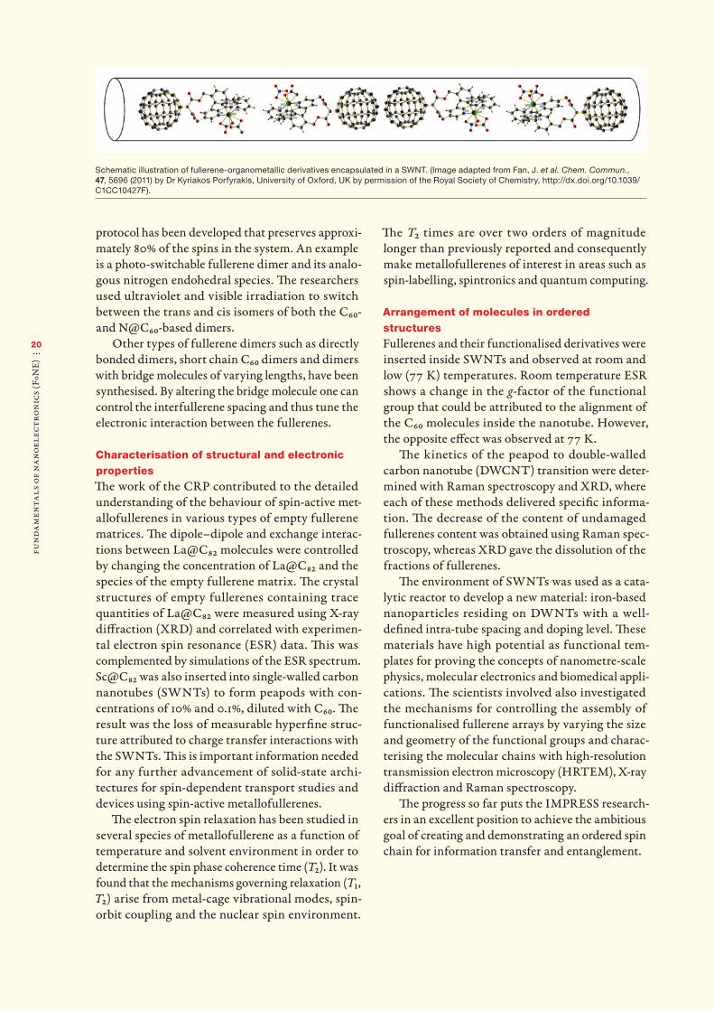
The scientific output spans three main experi-mental strands of research: the synthesis and chemistry of endohedral fullerenes, the characteri-sation of their structural and electronic properties and the arrangement of these molecules in ordered structures. Experimental work has been comple-mented by advanced quantum theory and molecular modelling.
Synthesis and chemistry of endohedral fullerenesWithin this CRP a whole series of new func-tionalised ful lerene derivatives, including endohedral fullerene derivatives, has been synthe-sised. (Endohedral fullerenes are fullerenes that have additional atoms, ions or clusters enclosed within their inner spheres. For example, N@C60 stands for a C60 fullerene with a nitrogen atom inside.) By tuning the conditions of the reactions, a
Fun
dam
enta
ls o
f N
an
oEle
ctro
nic
s (F
oNE)
20
protocol has been developed that preserves approxi-mately 80% of the spins in the system. An example is a photo-switchable fullerene dimer and its analo-gous nitrogen endohedral species. Th e researchers used ultraviolet and visible irradiation to switch between the trans and cis isomers of both the C60- and N@C60-based dimers.
Other types of fullerene dimers such as directly bonded dimers, short chain C60 dimers and dimers with bridge molecules of varying lengths, have been synthesised. By altering the bridge molecule one can control the interfullerene spacing and thus tune the electronic interaction between the fullerenes.
Characterisation of structural and electronic propertiesTh e work of the CRP contributed to the detailed understanding of the behaviour of spin-active met-allofullerenes in various types of empty fullerene matrices. Th e dipole–dipole and exchange interac-tions between La@C82 molecules were controlled by changing the concentration of La@C82 and the species of the empty fullerene matrix. Th e crystal structures of empty fullerenes containing trace quantities of La@C82 were measured using X-ray diff raction (XRD) and correlated with experimen-tal electron spin resonance (ESR) data. Th is was complemented by simulations of the ESR spectrum. Sc@C82 was also inserted into single-walled carbon nanotubes (SWNTs) to form peapods with con-centrations of 10% and 0.1%, diluted with C60. Th e result was the loss of measurable hyperfi ne struc-ture attributed to charge transfer interactions with the SWNTs. Th is is important information needed for any further advancement of solid-state archi-tectures for spin-dependent transport studies and devices using spin-active metallofullerenes.
Th e electron spin relaxation has been studied in several species of metallofullerene as a function of temperature and solvent environment in order to determine the spin phase coherence time (T2). It was found that the mechanisms governing relaxation (T₁, T2) arise from metal-cage vibrational modes, spin-orbit coupling and the nuclear spin environment.
Th e T2 times are over two orders of magnitude longer than previously reported and consequently make metallofullerenes of interest in areas such as spin-labelling, spintronics and quantum computing.
Arrangement of molecules in ordered structuresFullerenes and their functionalised derivatives were inserted inside SWNTs and observed at room and low (77 K) temperatures. Room temperature ESR shows a change in the g-factor of the functional group that could be attributed to the alignment of the C60 molecules inside the nanotube. However, the opposite eff ect was observed at 77 K.
Th e kinetics of the peapod to double-walled carbon nanotube (DWCNT) transition were deter-mined with Raman spectroscopy and XRD, where each of these methods delivered specifi c informa-tion. Th e decrease of the content of undamaged fullerenes content was obtained using Raman spec-troscopy, whereas XRD gave the dissolution of the fractions of fullerenes.
Th e environment of SWNTs was used as a cata-lytic reactor to develop a new material: iron-based nanoparticles residing on DWNTs with a well-defi ned intra-tube spacing and doping level. Th ese materials have high potential as functional tem-plates for proving the concepts of nanometre-scale physics, molecular electronics and biomedical appli-cations. Th e scientists involved also investigated the mechanisms for controlling the assembly of functionalised fullerene arrays by varying the size and geometry of the functional groups and charac-terising the molecular chains with high-resolution transmission electron microscopy (HRTEM), X-ray diff raction and Raman spectroscopy.
Th e progress so far puts the IMPRESS research-ers in an excellent position to achieve the ambitious goal of creating and demonstrating an ordered spin chain for information transfer and entanglement.
Schematic illustration of fullerene-organometallic derivatives encapsulated in a SWNT. (Image adapted from Fan, J. et al. Chem. Commun., 47, 5696 (2011) by Dr Kyriakos Porfyrakis, University of Oxford, UK by permission of the Royal Society of Chemistry, http://dx.doi.org/10.1039/C1CC10427F).
Fun
dam
enta
ls o
f N
an
oEle
ctro
nic
s (F
oNE)
21
Selected Publications
Buitelaar, M. R., Fransson, J., Cantone, A. L., Smith, C. G., Anderson, D., Jones, G. A. C., Ardavan, A., Khlobystov, A. N., Watt, A. A. R., Porfyrakis, K. and Briggs, G. A. D., Pauli spin blockade in carbon nanotube double quantum dots. Phys. Rev. B 77, 245439 (2008).
Cantone, A. L., Buitelaar, M. R., Smith, C. G., Anderson, D., Jones, G. A. C., Chorley, S. J., Casiraghi, C., Lombardo, A., Ferrari, A. C., Shinohara, H., Ardavan, A., Warner, J., Watt, A. A. R., Porfyrakis, K. and Briggs, G. A. D., Electronic transport characterization of Sc@C82 single-wall carbon nanotube peapods. J. Appl. Phys. 104, 083717 (2008).
Chamberlain, T. W., Pfeiffer, R., Peterlik, H., Kuzmany, H., Zerbetto, F., Melle-Franco, M., Staddon, L., Champness, N. R., Briggs, G. A. D. and Khlobystov, A. N., Polyarene-functionalized fullerenes in carbon nanotubes: towards controlled geometry of molecular chains. Small 4, 2262 (2008).
Gimenez-Lopez, M. C., Gardener, J., Iwasiewicz-Wabnig, A., Porfyrakis, K., Balmer, C., Dantelle, G., Shaw, A. Q., Hadjipanayi, M., Crossley, A., Champness, N. R., Castell, M. R., Briggs, G. A. D. and Khlobystov, A. N., Endohedral metallofullerenes in self-assembled monolayers. Phys. Chem. Chem. Phys. 12, 123 (2010).
Ito, Y., Warner, J. H., Brown, R., Zaka, M., Pfeiffer, R., Aono, T., Izumi, N., Okimoto, H., Morton, J. J. L., Ardavan, A., Shinohara, H., Kuzmany, H., Peterlik, H. and Briggs, G. A. D., Controlling intermolecular spin interactions of La@C82 in empty fullerene matrices. Phys. Chem. Chem. Phys. 12, 1618 (2010).
Robertson, J., Zhong, G., Telg, H., Thomsen, C., Warner, J. H., Briggs, G. A. D., Dettlaff-Weglikowska, U. and Roth, S., Growth and characterization of high-density mats of single-walled carbon nanotubes for interconnects. Appl. Phys. Lett. 93, 163111 (2008).
Shiozawa, H., Pichler, T., Grüneis, A., Pfeiffer, R., Kuzmany, H., Liu, Z., Suenaga, K. and Kataura, H., Catalytic reaction inside a single-wall carbon nanotube. Adv. Mater. 20, 1443 (2008).
Warner, J. H., Ito, Y., Rümmeli, M. H., Büchner, B., Shinohara, H. and Briggs, G. A. D., Capturing the motion of novel molecular nanomaterials encapsulated within carbon nanotubes with ultrahigh temporal resolution. ACS Nano 3, 3037 (2009).
Warner, J. H., Ito, Y., Rümmeli, M. H., Gemming, T., Büchner, B., Shinohara, H. and Briggs, G. A. D., One-dimensional confined motion of single metal atoms inside double-walled carbon nanotubes. Phys. Rev. Lett. 102, 195504 (2009).
Zaka, M., Warner, J. H., Ito, Y., Morton, J. J. L., Rümmeli, M. H., Pichler, T., Ardavan, A., Shinohara, H. and Briggs, G. A. D., Exchange interactions of spin-active metallofullerenes in solid-state carbon networks. Phys. Rev. B 81, 075424 (2010).
3.4 Domain Walls and Spin-Polarised Currents (SPINCURRENT)
Principal Investigators
•Christopher Marrows (Project Leader)•RolfAllenspach•MichaelCoey•VladimirFalko
Associated Partners
•MichelViret•DavidWilliams
Collaborator
•DafinéRavelosona
Funding Organisations
•Ireland: Enterprise Ireland•Switzerland: Swiss National Science Foundation•United Kingdom: Engineering and Physical
Sciences Research Council
The SPINCURRENT project was designed to investigate and exploit the transfer of spin angular momentum from a polarised current to a domain wall (a naturally occurring magnetic nanostructure) in metallic and semiconducting magnetic hetero-structures. The main focus was the nucleation and propagation of magnetic domain walls, and their interactions with spin-polarised currents. As well as being interesting from a fundamental point of view, this effect could be useful for writing data to high density non-volatile memories and performing switching operations in domain wall logic schemes.
The main aims of the project were:– to gain an understanding of how a domain
wall is moved by a spin-polarised current flow-ing through it, e.g., by spin-transfer torques and momentum transfer forces;
– to make use of this knowledge to find candidate materials and sample geometries that would make the effect suitable for technological exploitation;
Fun
dam
enta
ls o
f N
an
oEle
ctro
nic
s (F
oNE)
22
– to improve our understanding of how a domain wall in a nanometre-scale structure scatters spin-polarised carriers passing through it, and assess the usefulness of these effects for applications.
The researchers in this CRP have made significant advances in understanding the way that a magnetic domain wall is pinned in a confining potential provided by a notch in a nanowire. By combining nanofabrication, state-of-the-art magnetic imaging and ultrasensitive magnetotransport measurements, the groups led by Marrows and Allenspach have been able to quantify the force experienced by a domain wall during its depinning. The teams went on to show how to control this force by lithographic engineering of the shape and profile of the notch, and how to use this restoring force to provide high quality factor, well-defined resonances that yield a frequency-selective mode of operation for domain wall based spintronic technologies. The experi-mental and theoretical results produced in this work show that a domain wall can be treated to a good approximation as a quasiparticle acted on by a restoring force that may be derived from the notch shape in a physically transparent manner.
With today’s computing power, micromagnetic simulations are able to complement experiments with realistic models. The spin-transfer torque terms have been incorporated into the most widely used simulation tool, the freely available Object Oriented MicroMagnetic Framework (OOMMF) code. The new code extension allows users of the code to model current-induced domain wall motion. The work led – jointly with two other groups who also implemented their approach to spin-transfer torque into micromagnetic codes – to the proposal for a so-called “standard problem” in micromagnetism. This is a scheme which serves the community as a test bed for micromagnetic simulations. The work was published in the Journal of Applied Physics, and the code can be downloaded freely at http://www.zurich.ibm.com/st/magnetism/spintevolve.html.
The field of spintronics is naturally one that combines condensed matter physics, materials sci-ence and electronic engineering. SPINCURRENT was therefore intrinsically interdisciplinary, and brought together academics and industrial scientists with expertise spanning the range of fundamen-tal research to that closely linked to applications. The project created valuable collaborative links between world-class experimenters and theorists with diverse skills and expertise which are now producing high-quality scientific output, in the form of publications in high-impact journals and
conference talks. Regular meetings have led to the frequent exchange of ideas, students and know-how. Hence, whilst some work has been independently published, none of the work has taken place in isola-tion from other groups.
Selected Publications
Diao, Z., Nowak, E. R., Feng, G. and Coey, J. M. D., Magnetic noise in structured hard magnets. Phys. Rev. Lett. 104, 047202 (2010).
Feng, J. F., Diao, Z., Feng, G., Nowak, E. R. and Coey, J. M. D., Magnetic noise in MgO-based magnetic tunnel junction rings. Appl. Phys. Lett. 96, 052504 (2010).
Kuzmenko, I. and Falko, V., Canted magnetization texture in ferromagnetic tunnel junctions. Phys. Rev. B 78, 184425 (2008).
Lepadatu, S., Claydon, J. S., Kinane, C. J., Charlton, T. R., Langridge, S., Potenza, A., Dhesi, S. S., Keatley, P. S., Hicken, R. J., Hickey, B. J. and Marrows, C. H., Domain-wall pinning, nonadiabatic spin-transfer torque, and spin-current polarization in permalloy wires doped with vanadium. Phys. Rev. B 81, 020413 (2010).
Lepadatu, S., Hickey, M. C., Potenza, A., Marchetto, H., Charlton, T. R., Langridge, S., Dhes, S. S. and Marrows, C. H., Experimental determination of spin-transfer torque nonadiabaticity parameter and spin polarization in permalloy. Phys. Rev. B 79, 094402 (2009).
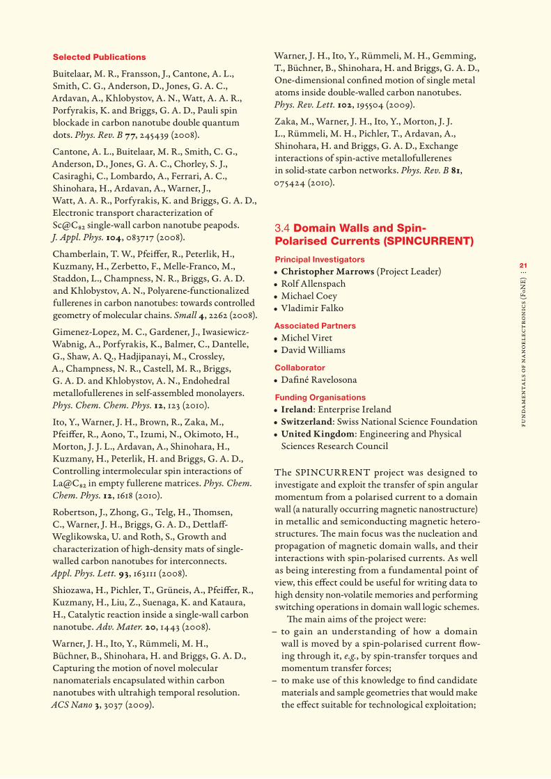
Domain wall pinning position at zero magnetic field after reversal from saturation, as a function of notch angle determined using micromagnetic simulations (top) and spin-SEM imaging (bottom). The spin-SEM images show the magnetisation direction along the length of the wire. From Lepadatu, S. et al. Phys. Rev. Lett. 102, 127203 (2009). Copyright (2009) by the American Physical Society.

Fun
dam
enta
ls o
f N
an
oEle
ctro
nic
s (F
oNE)
23
Lepadatu, S., Vanhaverbeke, A., Atkinson, D., Allenspach, R. and Marrows, C. H., Dependence of domain-wall depinning threshold current on pinning profile. Phys. Rev. Lett. 102, 127203 (2009).
Lepadatu, S., Wessely, O., Vanhaverbeke, A., Allenspach, R., Potenza, A., Marchetto, H., Charlton, T. R., Langridge, S., Dhesi, S. S. and Marrows, C. H., Domain-wall spin-torque resonators for frequency-selective operation. Phys. Rev. B 81, 060402 (2010).
Najafi, M., Krüger, B., Bohlens, S., Franchin, M., Fangohr, H., Vanhaverbeke, A., Allenspach, R., Bolte, M., Merkt, U., Pfannkuche, D., Möller D. P. F. and Meier, G., Proposal for a standard problem for micromagnetic simulations including spin-transfer torque. J. Appl. Phys. 105, 113914 (2009).
San Emeterio Alvarez, L., Wang, K. Y., Landi, S., Bending, S. and Marrows, C. H., Spin-transfer torque assisted domain wall creep in a Co/Pt multilayer wire. Phys. Rev. Lett. 104, 137205 (2010).
Vanhaverbeke, A., Bischof, A. and Allenspach, R., Control of domain wall polarity by current pulses, Phys. Rev. Lett. 101, 107202 (2008).
3.5 Spin-dependent Transport and Electronic Correlations in Nanostructures (SPINTRA)
Principal Investigators
•Bogdan Bulka (Project Leader)•FarkhadAliev•JozefBarnaś•TomaszDietl•VitNovák•GuntherSpringholz•ArturoTagliacozzo•ChrisVanHaesendonck
Associated Partners
•BryanGallagher•JoergWunderlich
Funding Organisations
•Austria: Austrian Science Fund•Belgium: Fonds voor Wetenschappelijk
Onderzoek – Vlaanderen •Czech Republic: Czech Science Foundation•Italy: National Research Council •Poland: Polish Academy of Sciences•Spain: Interministerial Committee on Science
and Technology
SPINTRA focused on fundamental aspects of spin-dependent transport and electronic correlations, and on effects which could lead to new devices for nanoelectronics. The team comprised experts in fabrication of magnetic nanodevices, measure-ments of spin-dependent transport and calculations of electronic transport, noise and current-induced switching effects.
Spin-polarised transport in hybrid nanostructuresOne aim of this CRP was to exploit the favourable properties of superconductor-semiconductor (Sc-Sm) junction compounds, e.g., very high dielectric constants and large effective g-factors, to construct spin filter devices. Low-temperature transport measurements in three-terminal devices showed unique characteristics at the PbTe/In interface unseen in other Sc-Sm systems. The devices revealed a superconducting transition at 6 K and supercon-ductivity persisted in the magnetic fields as high as 7 T. Additionally, it was shown that the In/PbTe interface is extremely transparent (96%), making it possible to observe pronounced conductance max-ima associated with the Andreev reflection.
The groups of Wunderlich, Gallagher and Novák designed an experiment to detect the inverse spin
Fun
dam
enta
ls o
f N
an
oEle
ctro
nic
s (F
oNE)
24
Hall effect (ISHE) of an optically excited spin-polarised current in a two-dimensional electron and hole gas system with variable Rashba-type spin-orbit coupling and a tuneable Fermi-level. This allowed them to study the presence of intrinsic and extrinsic sources of the ISHE and the transition between these two regimes. Moreover, a planar p–n diode microdevice was constructed and used to demonstrate that polarised injection of carri-ers can be detected by transverse electrical signals directly along the semiconducting channel, both inside and outside the injection area, without dis-turbing the spin-polarised current or employing magnetic elements. The device is a nonmagnetic spin-photovoltaic polarimeter that directly con-verts polarisation of light into transverse voltage signals. The spin Hall conductivity was also stud-ied in Tagliacozzo’s group. They investigated clean InGaAs samples by means of linear response theory. A new type of spin filter was proposed based on a quantum interference effect in an InGaAs ring in the presence of Rashba spin-orbit interaction and an external magnetic field orthogonal to the ring plane.
The groups led by Novák and Gallagher studied the epitaxial growth conditions of ferromagnetic GaMnAs in order to improve the magnetic and
transport properties of this spintronic material. By applying a special annealing technique to opti-mally grown GaMnAs layers the current world record Curie temperature of 187 K was achieved. Springholz’s group developed the growth of epitax-ial layers of another ferromagnetic semiconductor: GeMnTe with Mn concentrations from 0.5–100% (and Curie temperatures up to 190 K). The trans-port properties were studied in detail using anomalous and planar Hall effect and anisotropic magnetoresistance measurements, demonstrating spin-polarised free carriers in the samples.
Correlated electronic transport and current induced magnetic switching in nanoscale devicesAn important achievement by Van Haesendonck’s team is the identification of the “training effect” in the magnetic hysteresis loops of Co/CoO bilayers. This can be explained in terms of a model that takes into account that the CoO antiferromagnet consists of nanometre size grains, where the orientation of the anisotropy axes varies randomly from one grain to the other. The restoration of the untrained state can be directly visualised by magnetic force micros-copy at low temperatures and in the presence of a magnetic field.
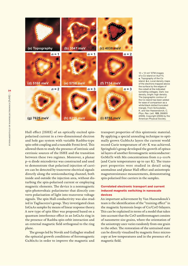
12 × 12 nm2 STM images of a Co island on Au(111). a, Topography of the Co island. b-i, Local density maps of the electrons trapped above the surface by the edges of the cobalt at the indicated tunnelling voltages. Dark: low density, bright: high density. The topographic contour of the Co island has been added for ease of comparison as a white/black dotted truncated triangle. From Schouteden, K. and Van Haesendonck, C. Phys. Rev. Lett. 103, 266805 (2009). Copyright (2009) by the American Physical Society.

Fun
dam
enta
ls o
f N
an
oEle
ctro
nic
s (F
oNE)
25
Among other successes, the project has high-lighted the fact that the electrical conductance of devices and nanostructured metal contacts repre-sents a powerful tool to detect nanomagnetism. A collaboration between the Polish groups resulted in the fabrication and low-temperature transport measurements of T-shaped three-terminal devices. By comparing the data to conductance modelling, it was confirmed experimentally that the T-shape is particularly well suited for studying and employing quantum effects which determine transport proper-ties of mesoscopic devices.
Current-induced switching and dynamics in spin valves were investigated – important effects for applications in spintronic devices such as micro-wave generators, magnetoresistive random access memory cells. Magnetic switching was shown to be a more general phenomenon, which appears in other magnetic systems, e.g., in magnetic mol-ecules attached to ferromagnetic leads. The problem of charge and spin correlations in electronic shot noise was studied experimentally by Aliev and theo-reticallybyBarnaśandBulka.Noisemeasurementsprovided a bridge between microscopic quantum properties of devices and macroscopic properties in the dynamics of domain walls, one of the major topics of other FoNE projects: SPINCURRENT and SpiCo.
The most recent achievement of SPINTRA used scanning tunnelling microscopy to detect confined image potential states trapped above magnetic Co islands on a Au(111) surface. Previous work estab-lished that electron clouds can escape from a metal surface and move freely above it; the team led by Van Haesendonck has now shown that the clouds can get trapped above a small nanometre-sized metal island. The team’s images revealed triangu-lar clouds trapped by the edges of a triangular Co island. The fuzzy edges of the clouds reflect the
“uncertainty” that is imposed by quantum mechan-ics, implying that the clouds can leak out from the triangular confinement.
Selected Publications
Acbas, G., Kim, M. H., Cukr, M., Novak, V., Scarpulla, M. A., Dubon, O. D., Jungwirth, T., Sinova, J. and Cerne, J., Electronic structure of ferromagnetic semiconductor Ga1-xMnxAs probed by subgap magneto-optical spectroscopy. Phys. Rev. Lett. 103, 137201 (2009).
Bonanni, A., Navarro-Quezada, A., Li, T., Wegscheider, M., Matej, Z., Holy, V., Lechner, R. T., Bauer, G., Rovezzi, M., D’Acapito, F., Kiecana, M., Sawicki, M. and Dietl, T., Controlled aggregation of magnetic ions in a semiconductor: An experimental demonstration. Phys. Rev. Lett. 101, 135502 (2008).
Brems, S., Temst, K. and Van Haesendonck, C., Origin of the training effect and asymmetry of the magnetization in polycrystalline exchange bias systems. Phys. Rev. Lett. 99, 067201 (2007).
Gmitra,M.andBarnaś,J.,Thermallyassistedcurrent-driven bistable precessional regimes in asymmetric spin valves. Phys. Rev. Lett. 99, 097205 (2007).
Grabecki, G., Kolwas, K. A., Wróbel, J., Kapcia, K., Puźniak, R., Jakieła, R., Aleszkiewicz, M., Dietl, T., Springholz, G. and Bauer, G., Contact superconductivity in In-PbTe junctions. J. Appl. Phys. 108, 053714 (2010).
Guerrero, R., Aliev, F. G., Villar, R., Santos, T.,Moodera,J.,Dugaev,V.K.andBarnaś,J.,Conductance in Co/Al2O3<Si>Al2O3 permalloy with asymmetrically doped barrier. Phys. Rev. B 81, 014404 (2010).
Lucignano, P., Giuliano, D. and Tagliacozzo, A., Quantum rings with Rashba spin-orbit coupling: a path integral approach. Phys. Rev. B 76, 045324 (2007).
Owen, M. H. S., Wunderlich, J., Novák, V., Olejník, K., Zemen, J., Výborný, K., Ogawa, S., Irvine, A. C., Ferguson, A. J., Sirringhaus, H. and Jungwirth, T., Low voltage control of ferromagnetism in a semiconductor p-n junction, New J. Phys. 11, 023008 (2009).
Schouteden, K. and Van Haesendonck, C., Quantum confinement of hot image-potential state electrons. Phys. Rev. Lett. 103, 266805 (2009).
Wrobel, J., Zagrajek, P., Czapkiewicz, M., Bek, M., Sztenkiel, D., Fronc, K., Hey, R., Ploog, K. H. and Bulka, B. R., Quantum effects in linear and nonlinear transport of T-shaped ballistic junction patterned from GaAs/AlxGa1-xAs heterostructures. Phys. Rev. B 81, 233306 (2010).


Fun
dam
enta
ls o
f N
an
oEle
ctro
nic
s (F
oNE)
27Networking and dissemination activities are key characteristics of a EUROCORES programme like FoNE. Their aim is to encourage and facili-tate scientific collaboration and diffusion across the Collaborative Research Projects within a given domain or, if appropriate, across different domains and programmes. These activities are flexible and can be tailored to the needs of a given programme.
Networking activities
These are collaborative activities bringing together scientists from EUROCORES programmes and col-leagues from other relevant programmes in order to discuss, plan and implement future collaboration and interaction.
Typical examples are:•Workinggroupmeetings,seminars,workshops,
symposia, conferences;•Summerschools (targetedtomembersofaca-
demia, the private sector and governmental or non-governmental organisations);
•Trainingprogrammesandspecialisedcourses(graduate-level and continuing-education);
•Shortvisits.
Dissemination activities
These are all the activities that are carried out with the aim of raising awareness and diffusing results of the EUROCORES programme. They include:• Leaflets, posters, publications, books, exhibition
booth or stand at a conference;•Invitedsessionsatlargerconferences(whenthe
EUROCORES programme is not directly involved in the conference as a main or co-organiser of the event;
•Disseminationtravelgrants,tosupportactivepar-ticipation at conferences (organised outside the EUROCORES programme), while promoting the EUROCORES Scheme in general and dis-seminating the achievements of the programme in particular.
For FoNE, the principal networking activity was a series of conferences, workshops and international schools that focused on various aspects of nanoelec-tronics. Among the dissemination activities were brochure publications, presentations by the princi-pal investigators as invited speakers at conferences and press releases. This section provides an over-view of the main networking and dissemination activities of FoNE.
4.Networking and Dissemination Activitiesl l l

Fun
dam
enta
ls o
f N
an
oEle
ctro
nic
s (F
oNE)
28
•Windsor Summer School: Quantum Transport and Dynamics in Nanostructures
Windsor, United Kingdom, 6-18 August 2007 http://www.lancs.ac.uk/users/esqn/windsor07/
This summer school reviewed the state-of-the-art in the theory of, and experiments on, quantum nano-systems and nano-structured materials. The course was designed to acquaint postgraduate and postdoctoral researchers with the recent progress in the following areas: •Electronicpropertiesoftherecentlydiscovered
new two-dimensional material, graphene, and the recent progress in the quantum Hall effect and spin-Hall effect in novel semiconductor struc-tures;
•The bosonisation technique and functionalrenormalisation group methods in application to Luttinger liquid in quantum wires and carbon nanotubes, and the theory of the Kondo effect;
•Theoryofquantuminformationprocessing,phasecoherence and de-coherence in qubits, coherent exciton dynamics and optical properties of quan-tum dots in microcavities;
•Adiabaticandnon-adiabaticdynamicsofquan-tum condensates of finite dimensions.
Lectures in theoretical methods were complemented by reviews of advanced experiments and research seminars. 29 researchers participated in the sum-mer school and students were encouraged to present their own work at poster sessions (preceded by brief introductory talks) and to compete for an Institute of Physics prize.
•Workshop: Quantum Transport, Magnetic Nanodevices and Spintronics
Naples, Italy, 10-13 December 2007 http://fone-cuma07.na.infm.it/
This cross-disciplinary workshop on quantum transport, magnetic nanodevices and spintronics brought together 68 researchers from three FoNE CRPs, SpiCo, SPINCURRENT and SPINTRA. The workshop aimed to cover state-of-the-art problems regarding the fabrication of spintronic devices, the interpretation of the physics involved in quantum electron transport of these systems and control with external sources. In particular, the very high possibility of coherent quantum manipula-tion of the spin; this requires a diffuse knowledge of the dissipation mechanisms involved and noise measurements could provide this information. Efficient spintronic devices should achieve control of magnetic domain walls or vortices by means of the spin current carried by the electrons, better than by a magnetic field. The workshop consisted of 28 lectures from invited speakers and research-ers from the CRPs. Among the invited experts in the field of nanoelectronics were Boris Altshuler (NEC-Columbia), Gerrit Bauer (TU Delft), Giancarlo Faini (Marcoussis), Yves Henry (LPMSM, Vandœuvre), Teruo Ono (Kyoto University), Dafiné Ravelosona (CNRS-Orsay), Maurice Skolnick (University of Sheffield) and Gen Tatara (Tokyo Metropolitan University). The workshop was very informal, offering space for debate, scientific exchange and diffusion of know-how.
More specifically, the following topics were addressed:•Magnetic semiconductorsand layeredmateri-
als, hybrid systems hetero-nano-structures, band structure and carriers, spin-orbit interaction, mag-netoconductance, anomalous Hall effect;
•Spincurrentsandmagneticdomainwalls,current-induced magnetic switching and dynamics in spin valves, spin torque, spin filtering, superconductor/ferromagnet proximity;

Fun
dam
enta
ls o
f N
an
oEle
ctro
nic
s (F
oNE)
29
•Quantum(spindependent)transportinconfinedgeometries, spin relaxation and spin manipulation in dots, wires and rings. Charge sensing, Kondo resonant tunnelling.
•Spring School: 4th Capri Spring School on Transport on Nanostructures
Naples, Italy, 30 March - 5 April 2008 http://tfp1.physik.uni-freiburg.de/Capri08/
This one-week Capri spring school on transport in nanostructures provided several five-hour lectures by leading experts supplemented by a few shorter seminars on transport in nanostructures. Electronic nanostructures are of considerable technologi-cal interest. With the decrease of the feature size of state-of-the-art electronic devices, nanostruc-tures will become more and more relevant to the semiconductor industry. The school had a special focus on graphene and electronic correlations in one- and two-dimensional materials. The speakers gave graduate-level presentations, introducing stu-dents to state-of-the-art methods and techniques used to describe non-equilibrium phenomena in low dimensional electronic devices. The number of par-ticipants in the spring school was limited to 35 and while the school was primarily aimed at instruct-ing PhD students and young postdocs, more senior scientists who wanted to acquaint themselves with the subject of the school were also welcome. 20 par-ticipants belonged to the FoNE programme and the school was seen to strengthen European physical sciences in this promising area of research.
•1st FoNE Conference on Nanoelectronics 2008 Taormina, Italy, 29 June - 3 July 2008
http://www.esf.org/fone
The 1st FoNE conference, Nanoelectronics 2008, took place mid-way through the programme and attracted 56 participants. It gathered physicists, chemists and electrical engineers together for three days to discuss and present research results in nano-electronics in the broadest sense. This included both the investigation of the unique properties of matter at the nanoscale, and the quest for a technology to realise terascale integrated systems.
All topics relevant to FoNE projects were addressed, so that the conference was an oppor-tunity to put activities in FoNE in the context of international research on nanoelectronics. Among the invited speakers in the field were Professor Rolf Haug (University of Hannover), Professor Jonathan Bird (State University of New York), Professor Guido Meier (University of Hamburg), Professor Joerg Appenzeller (Purdue University) and Dr Jamie Warner (University of Oxford).
•SpiCo, SPINCURRENT and SPINTRA Workshop Palermo, Italy, 14-17 December 2008
http://www.esf.org/fone
The FoNE projects SpiCo, SPINCURRENT and SPINTRA recognised that added value to their action could come from a joint meeting; this was held in Palermo in December 2008. 33 researchers participated in the workshop with interests spanning state-of-the-art problems regarding the fabrication of spintronic devices, the interpretation of the phys-ics involved in quantum electron transport of these systems and control with external sources.
The workshop included key-note talks from lead-ing scientists in the field, presentations by FoNE scientists covering the latest results and a poster session with contributions from junior researchers. It was an opportunity for the scientists to network, exchange results and develop new collaborations.
Fun
dam
enta
ls o
f N
an
oEle
ctro
nic
s (F
oNE)
30
•International School and Conference: Spintronics and Quantum Information Technology (SPINTECH)
Krakow, Poland, 7-11 July 2009 http://info.ifpan.edu.pl/spintech5/
Akin to the previously successful SPINTECH con-ferences, SPINTECH 5 highlighted fundamental physical phenomena related to spin-dependent effects in semiconductors and advances in the devel-opment of new semiconductor spintronic materials, structures and devices. This included quantum information hardware and concepts. The school took place during the first half of the week to orient students in this emerging field, and was followed by a conference aimed at stimulating progress in the fabrication, measurement and theory of semicon-ductor spintronic systems.
•FoNE Final Conference Madrid, Spain, 9-13 September 2009
www.uam.es/otros/foneconf/
The 2nd and final FoNE conference in Miraflores (Madrid) was organised by Professor Farkhad Aliev (SPINTRA member), and co-organised by Professor Christopher Marrows (SPINCURRENT mem-ber) and Professor Merlyne de Souza (DEWINT member). It formed an excellent platform for dis-semination of some of the latest developments in the fields of spintronics and nanoelectronics, and discussed means of continuing activity beyond the end of the FoNE EUROCORES programme.
The main goals of the final FoNE conference in Madrid were two-fold:•Dissemination of results and activities. All
five main collaborative projects which formed FoNE, i.e., SPINTRA, SPINCURRENT, SpiCo, IMPRESS and DEWINT, each organised a half-day scientific session. In these, in addition to 20-30 minute talks summarising project outcomes, invited external speakers (about one for each of the projects) gave more extended expert overviews. In this aspect, the final FoNE conference was simi-lar to the first one held in Taormina, Italy, in 2008.
•Discussionof (i) thecontinuationofnetworkactivities beyond the end of the projects and (ii) final reporting. In addition to local project meet-ings, joint meetings of principal investigators/project leaders from all research groups were organised to discuss plans for further research collaboration.
The research groups participating in this conference came from distinct fields of nanoscale physics, mag-netism, superconductivity and molecular electronics. This meant that the final ESF-FoNE conference pro-vided a forum for further cross-fertilisation between leading European research groups working in fun-damentals of nanoelectronics and the exploration of emerging themes. Additionally, the organising committee invited several experts from industry to
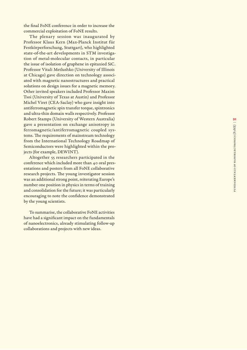
Fun
dam
enta
ls o
f N
an
oEle
ctro
nic
s (F
oNE)
31
the final FoNE conference in order to increase the commercial exploitation of FoNE results.
The plenary session was inaugurated by Professor Klaus Kern (Max-Planck Institut für Festkörperforschung, Stuttgart), who highlighted state-of-the-art developments in STM investiga-tion of metal-molecular contacts, in particular the issue of isolation of graphene in epitaxied SiC. Professor Vitali Metlushko (University of Illinois at Chicago) gave direction on technology associ-ated with magnetic nanostructures and practical solutions on design issues for a magnetic memory. Other invited speakers included Professor Maxim Tsoi (University of Texas at Austin) and Professor Michel Viret (CEA-Saclay) who gave insight into antiferromagnetic spin transfer torque, spintronics and ultra-thin domain walls respectively. Professor Robert Stamps (University of Western Australia) gave a presentation on exchange anisotropy in ferromagnetic/antiferromagnetic coupled sys-tems. The requirements of mainstream technology from the International Technology Roadmap of Semiconductors were highlighted within the pro-jects (for example, DEWINT).
Altogether 55 researchers participated in the conference which included more than 40 oral pres-entations and posters from all FoNE collaborative research projects. The young investigator session was an additional strong point, reiterating Europe’s number one position in physics in terms of training and consolidation for the future; it was particularly encouraging to note the confidence demonstrated by the young scientists.
To summarise, the collaborative FoNE activities have had a significant impact on the fundamentals of nanoelectronics, already stimulating follow-up collaborations and projects with new ideas.

Fun
dam
enta
ls o
f N
an
oEle
ctro
nic
s (F
oNE)
335.1 Royal Society Summer Science Exhibition 2008 “Wonder in carbon land: how do you hold a molecule” (London, 30 June – 3 July 2008)
The annual Summer Science Exhibition of The Royal Society is the Society’s main public event of the year and is open to members of the general public as well as students, teachers, scientists, policymakers and the media. It brings together members of the pub-lic and teams of researchers at the cutting-edge of science and technology and therefore provides a unique opportunity for the public to interact with scientists and ask them questions about their work.
Professor Andrew Briggs (IMPRESS) along with researchers from both the University of Oxford and the University of Nottingham organised Wonder in carbon land: how do you hold a molecule, one of 23 science exhibits at the 2008 event. Structural models at the event helped the team explain the advanced technology of carbon nanotubes and nanocages, and they have produced several worksheets that are available to download.
> More information at:•http://royalsociety.org/Wonder-in-carbon-land-
how-do-you-hold-a-molecule/•http://www.nottingham.ac.uk/nanocarbon/
freestuff.html
5.2 Interviews in printed and online newspapers/journals
•Professor Jozef Barnaś (SPINTRA) gave aninterview on his contribution to spintron-ics to a national newspaper, Gazeta Wyborcza, 12-13th April 2008, written by Adam Kompowski.
•ProfessorArturoTagliacozzo(SPINTRA)gaveaninterview on spintronics to the national newspaper, Il Mattino, on the occasion of the EUROCORES FoNE Workshop ‘Cuma: Quantum Transport, Magnetic Nanodevices and Spintronics’, 9-13th December 2007, Pozzuoli, Italy. The article appeared on 8th December 2007, page 50.
•ProfessorBogdanBułka (SPINTRA)gaveaninterview on spintronics to a local newspaper, Wyspiarz, number 45 (327), 6-12th November 2007, page 13.
5. Outreach Activities l l l
From Britz, D. A and Khlobystov, A. N. Chem. Soc. Rev. 35, 637 (2006), http://dx.doi.org/10.1039/b507451g. Reproduced by permission of the Royal Society of Chemistry.
Fun
dam
enta
ls o
f N
an
oEle
ctro
nic
s (F
oNE)
34
•BilayerGrapheneforTFETs,byBelleDumé,26 June 2009
http://nanotechweb.org/cws/article/tech/39595 (DEWINT).
•Graphene makes transistors tunable, by Neil Savage, IEEE Spectrum, September 2009 (in print and online:
http://spectrum.ieee.org/semiconductors/materials/graphene-makes-transistors-tunable) (DEWINT).
•Warner,J.H.,Schaffel,F.,Zhang,G.,Rümmeli,M. H., Büchner, B., Robertson, J. and Briggs, G. A. D. Investigating the diameter-dependent stability of single-walled carbon nanotubes. ACS Nano 3, 1557 (2009).
Nanowerk Spotlight 25 June 2009. www.nanowerk.com/spotlight/spotid=11356.php
(IMPRESS).
•JointLeeds/IBMpressrelease‘Beatingtheback-upblues’ (http://www.leeds.ac.uk/news/article/59/beating_the_back-up_blues), which was widely syndicated on online technology news websites. (SPINCURRENT).
•ScientifichighlightsattheDiamondLightSourcesynchrotron (SPINCURRENT)
http://www.diamond.ac.uk/Home/Beamlines/I06/casestudies/magnetic_devices.html
http://www.diamond.ac.uk/Home/Beamlines/I06/casestudies/magnetism.html.
•ProfessorFarkhadAliev,‘Nanociencia:Elfuturode detectores ultrasensibles de campo magnético’, Unidad de Cultura Científica de la Universidad Autónoma de Madrid.
http://www.madrimasd.org/informacionidi/noti-cias/noticia.asp?id=39003&tipo=g
http://www.universia.es/html_estatico/portada/actualidad/noticia_actualidad/param/noticia/jjiai.html
http://www.navarrainnova.com/es/acercate/actu-alidad/2009/04/20/15347.php
http://www.fys.es/fys/cm_view_tnoticia.asp?id= 2005495 (SPINTRA).
•RaulVillar,‘Lossecretosqueaúnescondenlossuperconductores’, Unidad de Cultura Científica de la Universidad Autónoma de Madrid.
http://www.uam.es/ss/Satellite/es/12348863444 85/1242648658587/notcientifica/notCientific/ 1242648658587.htm (SPINTRA).
5.3 Public websites
•Theprojectleadershavetheirownwebpages,wherethegoals and the activities of their projects are presented (e.g., SPINTRA: www.ifmpan.poznan.pl/spintra/). The most interesting achievements of all five CRPs are also presented on the ESF web page devoted to the EUROCORES FoNE programme (www.esf.org/fone).
•FerromagneticSemiconductorSpintronicsWebProject: Free international database of semicon-ductor spintronics publications, theoretical and experimental data.
> More information at:http://unix12.fzu.cz/ms/index.phphttp://unix12.fzu.cz/msold/index.php
5.4 Other outreach activities
•Patent:pending “Proximity Josephson sensor”, presented at The
National Board of Patents and Registration of Finland (www.prh.fi) on 15th February 2008 (application number FI20080124).
•Inventors:F.Giazotto(NESTCNR-INFMPisa),G. P. Pepe (CNR-INFM Coherentia, Napoli), T. Hekkila (TKK, LT Lab, Finland), P. Helistu (VTT IT, Finland), E. A. Luukanen (VTT MilliLab, Finland). (http://patent.prh.fi/patinfo/default.asp).
•TheOxfordarc-dischargereactorforsynthesisof carbon nanomaterials features in a Nanoseries video clip about carbon nanotubes that can be seen at the following address:
http://www.youtube.com/watch?v=B4VTfgaKLAM&feature=related (IMPRESS).
•DrBenjamin,withinputfromDrMorton,hasproduced four podcasts on Nanotechnology on http://itunes.ox.ac.uk/ (IMPRESS).

Fun
dam
enta
ls o
f N
an
oEle
ctro
nic
s (F
oNE)
35This section provides a summary of five activities at the ESF – either recently completed or currently ongoing – in the field of condensed matter phys-ics. Where possible, information is disseminated between these activities and those of FoNE in order to promote links between them.
6.1 Research Networking Programmes
Research Networking Programmes are another instrument of the ESF, which comprise networking activities of four to five years to lay the foundations for nationally funded research groups to address major scientific and research infrastructure issues. They can involve:•Sciencemeetings (workshops, conferencesor
schools);•Grantsforbothshortvisitsandlongerexchange
visits;•Publicationofinformationbrochuresandleaflets;•Creationandmaintenanceofscientificdatabases
at the European level.
6.1.1 Arrays of Quantum Dots and Josephson Junctions (AQDJJ)AQDJJ was an interdisciplinary Research Network-ing Programme aimed at identifying frontiers and future needs in condensed matter, low tempera-ture and nonlinear physics. In particular, special attention was given to novel photonic methods of optical and microwave characterisation of these arrays which are contactless, fast, informa-tive and, therefore, efficient and simple to use.
AQDJJ joined both theoretical and experimental efforts with the aim:•Toexploreandunderstand thestructureand
dynamics of low energy excitations in these sys-tems, with special emphasis on the physics of various complex Josephson systems, such as Josephson ladders, long Josephson junctions and others in different geometries and types of back-ground;
•Tocontinueintensiveinvestigationsonthegrowthof arrays of nanoparticles and quantum dots, and other properties of nanostructures;
•Todevelopacompletepictureoflowandhighenergy excitations of Josephson junction arrays and other nanostructures by focusing on three topics:– physics of the interaction of light and micro-
wave radiation with nanoparticles, quantum dots and Josephson arrays, characterisation of these arrays and optical manipulation of their properties especially in the quantum regime;
– structure and excitations in quantum dots and Josephson arrays, pattern formation and self-organisation;
– physics of the growth and self-organisation of arrays of quantum dots and nanoparticles within organic matrices.
The ESF AQDJJ Research Networking Programme ran for five years from June 2004 to June 2009.
> More information at: www.esf.org/aqdjj.
6. Related ESF Activities l l l
Fun
dam
enta
ls o
f N
an
oEle
ctro
nic
s (F
oNE)
36
6.1.2 Interdisciplinary Statistical and Field Theory Approaches to Nanophysics and Low-Dimensional Systems (INSTANS)INSTANS was an interdisciplinary Research Networking Programme aimed at identifying frontiers and future needs in condensed matter, quantum field theory and statistical physics.
INSTANS aimed: •Tostudyelectronicsystems,suchasnanotubes,
quantum dots and quantum Hall effect devices, as well as specific devices featuring cold atoms. These systems are dominated by quantum effects and strong interactions, which give rise to non-perturbative effects, such as spin-charge separation or fractionally charged excitations;
•Tosharpenanewsetofpowerfulnon-pertur-bative theoretical methods recently developed within the area of statistical field theory;
•Tosetupanewtheoreticalframeworktoanswerthe fundamental questions encountered in the modern physics of nanoscopic and low-dimen-sional systems.
The ESF INSTANS Research Networking Pro-gramme ran for five years from October 2005 to October 2010.
> More information at: www.esf.org/instans.
6.1.3 Nanoscience and Engineering in Superconductivity (NES)NES is a Research Networking Programme aimed at identifying the fundamental relations between quantised confined states and the physical prop-erties of superconducting quantum coherent systems.
NES aims: •Toinvestigateconfinedcondensateandfluxin
superconductors at the nanoscale by using vari-ous confinement patterns introduced artificially in the form of individual nanoplaquettes, their clusters and huge arrays;
•Tostudythedependenceofthequantisationeffects on the confinement length scale and the geometry;
•Totunetheboundaryconditions,definingtheconfinement potential, by using the hybrid super-conductor/normal and superconductor/magnet interfaces in superconducting nanosystems;
•To reveal the evolution of superconductiv-ity at the nanoscale by determining the size dependence of the superconducting critical tem-perature and the gap in mass selected clusters
and nanograins and also by studying superfluid-ity in different restricted geometries;
•Toinvestigatethefluxconfinementbymagneticdipoles and other periodic pinning arrays in super-conductors.
The ESF NES Research Networking Programme will run for five years from May 2007 to May 2012.
> More information at: www.esf.org/nes.
6.1.4 Quantum Spin Coherence and Electronics (QSpiCE)QSpiCE is a Research Networking Programme aimed at identifying frontiers and future needs in quantum information processing, coherent quan-tum transport and correlation phenomena.
QSpiCE aims:•Toinvestigatequantumspin-dependenteffects
and transport in nanoscale structures such as semiconducting nanowires, carbon nanotubes, quantum dots and graphene nanoribbons;
•Toimprovethemanipulationandthecontrolofthe electron or hole spin in nanostructures and at analysing and harnessing the various mecha-nisms leading to relaxation and decoherence of spin in nanoscale objects;
•TostrengthennetworkingbetweentheleadingEuropean groups in the field and thus increase their influence in this important and popular field of modern condensed matter physics.
The ESF QSpiCE Research Networking Programme will run for five years from June 2009 to June 2014.
> More information at: www.esf.org/qspice.

Fun
dam
enta
ls o
f N
an
oEle
ctro
nic
s (F
oNE)
37
6.2 EUROCORES Programme: EuroGRAPHENE
EuroGRAPHENE is a three-year programme, which recognises that there is a clear need for European-wide cooperation to tackle the chal-lenges of deepening current understanding of the physical properties of graphene; expanding research into new areas of chemically modifying the material and searching for methods to design its electronic properties; investigating its mechanical and electro-mechanical properties, broadly studying kinetic processes in graphene aiming at understanding optoelectronic eff ects; and modelling graphene-based devices for any functional applications.
EuroGRAPHENE provides the framework for bringing together the complementary expertise of technologists, experimentalists and theorists within small and medium-size consortia of world-leading European research groups. In doing so it aims to accelerate the pace of European research in gra-phene and its applications by concentrating and networking the activities.
Th e EuroGRAPHENE EUROCORES programme will run for three years from June 2010 to June 2013.
> More information at: www.esf.org/eurographene
The physical structure of graphene consists of a single layer of carbon atoms densely packed in a honeycomb crystal lattice (Courtesy of V. Palermo, ISOF, Bologna, Italy).
The physical structure of graphene consists of a
EUROCORES Programme
EuroGRAPHENEMaximising the Impact of Graphene Research in Science and Innovation


Fun
dam
enta
ls o
f N
an
oEle
ctro
nic
s (F
oNE)
39
Annex

Fun
dam
enta
ls o
f N
an
oEle
ctro
nic
s (F
oNE)
40
FoNE Review Panel Consensus ReportStrasbourg, 11 May 2010
The Fundamentals of Nanoelectronics (FoNE) pro-gramme has been a success in producing world-class scientific achievements, augmented by the added European dimension.
There was good progress throughout the three years achieving many of the originally proposed objectives. Major publications appeared in high quality journals spanning the duration of the program. ESF networking activities played an important role in facilitating collaboration and information sharing.
The five Collaborative Research Projects (CRPs) covered most scientific activities within the area of fundamental nanoelectronics. Although major projects on nanoscale photonics and superconduc-tivity could not be included explicitly, due to limited resources, they were indirectly addressed within some projects.
1. Specific scientific achievements
There were several internationally-competitive highlights from the CRPs. Notable examples, with potential for future applications, include:•Realisationofspinchainsonfullerenes,encap-
sulated in carbon nanotubes (peapods) and measurement of spin properties.
•Demonstrationofafrequency-dependentspintorque resonator based on current-threshold mag-netic domain-wall pinning physics.
•Creationofaquantumresistancestandardusinggraphene on silicon carbide.
•Realisationofnon-volatilecontrolofferromag-netism with a ferroelectric gate – a new kind of multiferroic system.
•Theoreticaldemonstrationofachannelfieldeffecttransistor using a graphene nanoribbon.
•WorldrecordCurietemperature(188K)forafer-romagnetic semiconductor.
•Creationofanon-magneticspin-photovoltaicpolarimeter that provides a direct electrical meas-urement of light polarisation.
2. Networking, training and dissemination
Nanoelectronics is a broad and worldwide rapidly developing field of research. Effective networking and broad dissemination of research results is vital to maintain momentum and to avoid duplication of research activities. The main achievements of the collaboration as a whole had been made pos-sible through exchanges, sharing of resources and complementary expertise.
Networking has generally been good, though by no means consistent throughout the five consor-tia, varying from essentially (only) preparation and attendance at the FoNE conferences (DEWINT) to multiple bi-partite exchanges within the most actively networking collaborations (SPINTRA).
Examples of the networking activities are the various workshops, schools, and conferences organ-ised in the framework of the FoNE programme:•The1st FoNE conference “Nanoelectronics” (July
2008) in Taormina, Sicily, organised by the 5 CRP’s participating in the EUROCORES FoNE programme.
•ThePozzuoliworkshop(December2007)on“Quantum Transport, Magnetic Nanodevices, and Spintronics” run jointly by SPINTRA, SpiCo, and SPINCURRENT.
•TheSPINTRAworkshoporganisedinPoznan(January 2007).
•The4th and 5th Windsor Summer Schools (August 2007, August 2010) organised by V. Falko (SpiCo).
•The Capri Spring School on “Transport inNanostructures” (March-April 2008) organised by A. Tagliacozzo (SPINTRA) and C. Marrows (SpinCurrent).
•The“FifthInternationalschoolandConferenceon Spintronics and Quantum Information Technology” (SPINTECH V) organised in Cracow (July 2009) by T. Dietl (SPINTRA) and D. Loss (SpiCo).
•ThefinalFoNeconferenceatMirafloresde laSierra (September 2009) organised by F. Aliev (SPINTRA) and co-organised by C. Marrows (SPINCURRENT) and M. de Souza (DEWINT) confirmed the importance and impact of the FoNE programme.
Fun
dam
enta
ls o
f N
an
oEle
ctro
nic
s (F
oNE)
41
Training was generally excellent, with students and early-stage researchers benefitting substantially from the opportunities to visit other groups and to attend the conferences and workshops which have been organised, both within and outside FoNE.
Dissemination of research results was generally very good although variable as might be expected from projects that are mainly very fundamental ori-ented. Researchers targeted high impact journals, whilst also giving an impressive number of confer-ence presentations, invited talks and posters.
The recipients of dissemination should include as much as possible a wider audience for the public understanding of science, but this was not always the case. There were a few examples where the excitement of nanoelectronics and quantum infor-mation was presented to a more general audience through newspaper articles and public demonstra-tions. Two notable examples of video lectures and podcasts have clearly struck a chord with the general public considering the number of downloads. More of these outreach activities would be welcome if we are to gain and maintain the support of European taxpayers.
To summarise, the collaborative FoNE activities have had a significant impact on the fundamentals of nanoelectronics, already stimulating follow-up collaborations and projects with new ideas.
3. Realisation of the FoNE programme’s potential
Enhanced interaction between research teamsThe EUROCORES FoNE programme has stimu-lated much activity among the project partners. The impact on the various research domains, in view of the relatively modest funding level, was very positive, initiating many innovative ideas. In this respect, a focused programme such as FoNE, is capable of making a significant contribution to the European research portfolio.
Most important was the activation of collabo-ration between the partners within the projects, combining theoretical and experimental research in order to lay the foundations for new nanoelec-tronic devices.
In general, all participants made good use of the FoNE programme which impacted very positively the various areas under examination. However, there was a wide variation in the level of collabora-tion within each CRP. In SPINCURRENT, SpiCo and SPINTRA, the level of collaboration was excel-lent, contributing much to their scientific success.
The FoNE programme provided the oppor-tunity to recruit PhD students and postdoctoral researchers, enabling the transfer of experimental and theoretical methods between different research laboratories. It also stimulated the dissemination of results, ideas and triggered new projects.
FoNE brought together leading European researchers creating a fertile ground for the fur-ther development of innovative ideas enhancing the dynamics and reputation of EUROCORES programmes. This stimulated proposals for new national and EU programmes as well as interna-tional collaborations.
The programme enabled different communi-ties, each with their own expertise, to pool and enhance their resources. This created conditions for the stimulation of research activities through-out Europe.
4. Suggestions to achieve optimal use of the EUROCORES programme’s experiences in potential future initiatives in this area
General•Theprogrammecouldbebetteradvertised.In
order to develop scientific research uniformly throughout Europe, strong research groups should be encouraged to integrate researchers from new member countries of the EU. Participation in EUROCORES programmes opens this possibility.
•TheroleofPanelMemberscouldbemoreactive,not only in evaluating proposals, midterm and final reports, but also in additional activities dur-ing the networking phase of the programme. Panel members were only invited to one FoNE confer-ence (Taormina 2008).
Specifica) Aims of the programme
•Moreemphasisshouldbegiveninthereportto the main objectives of the CRP e.g. how the research performed fitted within those goals of the programme.
•Both in reports and particularly at theEUROCORES programme conferences, the project leaders should provide a summary to remind the audience/reader of the aims of their CRP. This sets the scene of what progress has been made.
b) Benefit of the programme
•Itwouldbeinterestingtoreportinmoredetail
Fun
dam
enta
ls o
f N
an
oEle
ctro
nic
s (F
oNE)
42
how the programme is beneficial for the start of new initiatives (projects, collaborations), and for the future career of the researcher.
•Moreencouragementofuseoftheweblectures/demonstrations/podcasts/youtube would be wel-come. This is becoming increasingly important for the public understanding of science with a potentially massive European audience.
•ThePIsshouldsendshortresearchsummaries,say every 6 months, to the programme manager, summarising progress highlights, problems, next steps, new opportunities, etc. The template would be provided by the ESF.
c) Scientific output
•Itshouldbemadeclearfromthelistofpublica-tions in the report if: i) the list contains the total number of papers published by the partners in the consortium; ii) the list is restricted to papers directly related to the programme; iii) the list is restricted to those papers acknowledging the FoNE programme.
d) Collaborations
•It isgenerallydifficult toevaluatefromthereports the quality and quantity of collabora-tions. All CRPs should clearly report on the papers which include at least two different part-ners within the consortium. On presentations at conferences it would help to know which of these were collaborative with at least one other group.
•Inordertoinitiateeffectiveinteractions,afirstmeeting with all CRPs should be held within the first 6 months.
Final remarkThe evaluation panel would like to point out that the programme is effectively managed by the ESF staff, who are professional, receptive and very well organised.


European Science Foundation1 quai Lezay-Marnésia • BP 9001567080 Strasbourg cedex • FranceTel: +33 (0)3 88 76 71 00Fax: +33 (0)3 88 37 05 32www.esf.org
ISBN: 978-2-918428-44-2June 2011 – Print run: 500