esk32-a2a31 2.8 inch tft lcd module user manual e 4. lcd mod le + expansion boa d + sta te kit ........
TRANSCRIPT

ESK32-A2A31 2.8 Inch TFT LCD ModuleUser Manual
Revision: V1.00 Date: �e���a�� 0�� �01��e���a�� 0�� �01�

Rev. 1.00 � of 1� �e���a�� 0�� �01�
ESK3�-A�A31 �.� Inch T�T LCD Mod�leUse� Man�al
Table of Contents
Table of Contents1 Introduction ............................................................................................................. 5
2 Hardware Layout ..................................................................................................... 5Comm�nication Inte�face Switch – SW1 .......................................................................................... 6Extension Connecto� – CN� ............................................................................................................. 6
3 Using the Module .................................................................................................... 7Tool P�epa�ation ..................................................................................................................... 7LCD Mod�le Setting ............................................................................................................... 7Expansion Boa�d Setting ....................................................................................................... 7Boa�d Assem�l� ..................................................................................................................... 9O�tain the Example P�og�am ................................................................................................ 9Compile and Exec�te the P�og�am ...................................................................................... 10
4 Schematics ............................................................................................................ 10�.� Inches T�T LCD Mod�le – ESK3�-A�A31.................................................................................11

Rev. 1.00 3 of 1� �e���a�� 0�� �01�
ESK3�-A�A31 �.� Inch T�T LCD Mod�leUse� Man�al
List of Tables
List of TablesTa�le 1. Comm�nication Inte�face Switch SW1 ........................................................................................ 6Ta�le �. Extension Connecto� CN� ........................................................................................................... 6Ta�le 3. Expansion Boa�d EBI Inte�face Switches .................................................................................... �

Rev. 1.00 4 of 1� �e���a�� 0�� �01�
ESK3�-A�A31 �.� Inch T�T LCD Mod�leUse� Man�al
List of Figures
List of Figures�ig��e 1. T�T LCD Mod�le La�o�t ........................................................................................................... 5�ig��e �. Extension Connecto� CN� ......................................................................................................... 6�ig��e 3. LCD Mod�le Comm�nication Inte�face Setting ......................................................................... 7�ig��e 4. LCD Mod�le + Expansion Boa�d + Sta�te� Kit ........................................................................... 9�ig��e 5. HT3� �i�mwa�e Li��a�� Download We� Link ........................................................................... 10�ig��e 6. �.� Inches T�T LCD Mod�le (ESK3�-A�A31) Schematic ........................................................11

Rev. 1.00 5 of 1� �e���a�� 0�� �01�
ESK3�-A�A31 �.� Inch T�T LCD Mod�leUse� Man�al
Introduction
1 IntroductionThe ESK32-A2A31 TFT LCD Module is designed for the HT32 series expansion board. It supports SPI and EBI communication interfaces. The ESK32-A2A31 hardware and software can be used with the ESK32-20001/ESK32-21001 and the HT32 firmware library, providing users with a complete development environment with which to learn how to use the EBI and SPI interfaces.
Specifications:
▆ Use Himax’s TFT LCD driver IC: HX8347-I (T) ▆ 2.8 inch TFT LCD with 65 K colours and 320×240 resolutions ▆ Supports SPI and EBI interfaces
2 Hardware Layout
Figure 1. TFT LCD Module Layout

Rev. 1.00 6 of 1� �e���a�� 0�� �01�
ESK3�-A�A31 �.� Inch T�T LCD Mod�leUse� Man�al
Hardw
are Layout
Communication Interface Switch – SW1Table 1. Communication Interface Switch SW1
Switch No.Description
1 2 3 40 0 0 x �0�0 MCU 16-�it pa�allel1 0 0 x �0�0 MCU �-�it pa�allelID 0 1 x 3-wi�e se�ial inte�facex 1 1 x 4-wi�e se�ial inte�face
x: Don‘t ca�e
Extension Connector – CN2
Figure 2. Extension Connector CN2
Table 2. Extension Connector CN2Pin No. Description Pin No. Description
1 VDD5 � GND3 BL_EN 4 NC5 NC 6 WR/SCL7 MISO � MOSI9 /CS 10 NC11 NC 1� /Reset13 GND 14 VDD3315 PD0 16 PD117 PD� 1� PD319 PD4 �0 PD5�1 PD6 �� PD7�3 PD� �4 PD9�5 PD10 �6 PD11�7 PD1� �� PD13�9 PD14 30 PD1531 PD16 3� PD1733 /RD 34 RS

Rev. 1.00 7 of 1� �e���a�� 0�� �01�
ESK3�-A�A31 �.� Inch T�T LCD Mod�leUse� Man�al
Using the M
odule
3 Using the Module
Tool PreparationUsers need to prepare the HT32 Series expansion board (ESK32-2x001) and the Starter Kit (ESK32-30xxx)
LCD Module SettingBefore adjusting the communication interface using SW1, refer to the following descriptions and figure 3 for the LCD module setting details.
If the MCU uses the EBI interface to drive the LCD module, the LCD module should be selected to be in the EBI mode by switching SW1 of the LCD module to “0000” (default setting).
If the MCU uses the SPI interface to drive the LCD module, the LCD module should be selected to be in the SPI mode by switching SW1 of the LCD module to “0010”.
Figure 3. LCD Module Communication Interface Setting
Expansion Board SettingThe expansion board settings, J1, J2 and J3 are associated with the LCD module, refer to table 3 for more details. Refer to the “ESK32-2x001 Expansion Board User Manual” for details on using this expansion board.
J1: This is used to select whether the LCD Backlight is controlled by the MCU I/O pins or not. When the MCU I/O pins are insufficient, J1 can be switched to the BL_ON position, ensuring that the LCD Backlight is always on.
J2: This is used for the EBI interface read operation and determines the MCU EBI OE pin is connected to the nRD pin of the LCD module or not. When the LCD module needs to read back the registers or display the RAM, J2 should be switched to OE.
J3: If the MCU supports the EBI interface, then J3 should be open, otherwise J3 should be shorted.

Rev. 1.00 � of 1� �e���a�� 0�� �01�
ESK3�-A�A31 �.� Inch T�T LCD Mod�leUse� Man�al
Using the M
odule
Table 3. Expansion Board EBI Interface SwitchesJumpers Descriptions
J1
LCD Backlight will alwa�s �e on
LCD Backlight cont�olled �� I/O pin
J�
The LCD mod�le nRD pin is switched to the EBI OE pin
The LCD module nRD pin is switched to a fixed pull high
J3
Sho�t: LCD SPI mode
Open: LCD EBI mode
Rev. 1.00 9 of 1� �e���a�� 0�� �01�
ESK3�-A�A31 �.� Inch T�T LCD Mod�leUse� Man�al
Using the M
odule
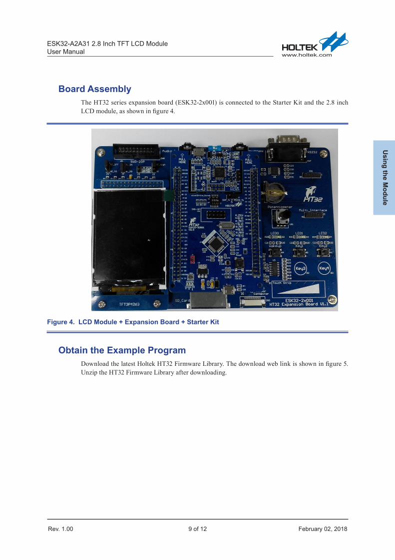
Board AssemblyThe HT32 series expansion board (ESK32-2x001) is connected to the Starter Kit and the 2.8 inch LCD module, as shown in figure 4.
Figure 4. LCD Module + Expansion Board + Starter Kit
Obtain the Example ProgramDownload the latest Holtek HT32 Firmware Library. The download web link is shown in figure 5. Unzip the HT32 Firmware Library after downloading.

Rev. 1.00 10 of 1� �e���a�� 0�� �01�
ESK3�-A�A31 �.� Inch T�T LCD Mod�leUse� Man�al
Schematics
Figure 5. HT32 Firmware Library Download Web Link
Compile and Execute the ProgramOpen the LCD example project:
Keil: \example\LCD\LCD28\MDK_ARMvx\Project_xxxxx.uvprojx
IAR: \example\LCD\LCD28\EWARMvx\Project_xxxxx.eww
Compile and execute the LCD example program after which, “Holtek HT32 Series LCD Example” will appear on the LCD.
4 SchematicsThis section shows the LCD module circuitry.

2.8 Inches TFT LCD Module – ESK32-A2A31
Mount only for SPI interfaceMount only for parallel interface
0 0 0 80-System 16-bit ⅠIM2 IM1 IM0 Interface Mode
0 0 1 80-System 8-bit Ⅰ 1 0 ID 3-Wire serial Ⅰ 1 1 X 4-Wire serial Ⅰ
LE
D_A
PD
0P
D1
PD
2P
D3
PD
4P
D5
PD
6P
D7
PD
8P
D9
PD
11
PD
12
PD
13
PD
14
PD
15
PD
16
PD
17
SD
I
WR
/SC
L/R
D
/RE
SE
T
RS
/CS
WR/SCL
/CS
/RD
RS
EN
/CS
PD0PD2PD4PD6PD8PD10PD12PD14PD16/RD RS
PD17PD15PD13PD11PD9PD7PD5PD3PD1
/RESET
WR/SCLSDISDO
SD
O
LE
D_K
1LE
D_K
2LE
D_K
3LE
D_K
4
PD
10
PD
15
PD
14
PD
13
PD
12
PD
11
PD
10
PD
9P
D8
PD
7P
D6
PD
5P
D4
PD
3P
D2
PD
1P
D0
PD
16
PD
17
LED_A
EN
LED_K1
LED_K2
LED_K3
LED_K4
VDD33VDD33
VDD33
VDD33
RN1
RP4K7
RN1
RP4K7
18
27
36
45
R3
10K/5%/0603
R3
10K/5%/0603
R8 75/5%/0603R8 75/5%/0603
C3
1uF/0603
C3
1uF/0603
C2 1uF/0603C2 1uF/0603
R1
4K
7/0
603
R1
4K
7/0
603
R11 75/5%/0603R11 75/5%/0603
R74K7/0603R74K7/0603
U1
HT7936
U1
HT7936
VOUT1
GND2
EN3
C-4VIN5C+6
CN2
LCM HEADER 17X2
CN2
LCM HEADER 17X2
VDD51
GND02
BL_EN3
I2C_SDA4
I2C_SCL5
WR/SCL6
MISO7
MOSI8
/CS9
PENIRQ10
NC011
/RESET12
GND113
VDD3314
PD015
PD116
PD217
PD318
PD419
PD520
PD621
PD722
PD823
PD924
PD1025
PD1126
PD1227
PD1328
PD1429
PD1530
PD1631
PD1732
/RD33
RS34
RN2
RP4K7
RN2
RP4K7
18
27
36
45
SW1
SW DIP-4
SW1
SW DIP-4
R10 75/5%/0603R10 75/5%/0603
R9 75/5%/0603R9 75/5%/0603
RN5
RP4K7
RN5
RP4K7
18
27
36
45
C1
1uF/0603
C1
1uF/0603
RN3
RP4K7
RN3
RP4K7
18
27
36
45
R54K7/0603R54K7/0603
R44K7/0603R44K7/0603
R2
4K
7/0
603
R2
4K
7/0
603
+
C410uF/CASE-A
+
C410uF/CASE-A
RN4
RP4K7
RN4
RP4K7
18
27
36
45
CN1
TFT3P4263 /40PIN
CN1
TFT3P4263 /40PIN
LE
DA
1
LE
DK
12
LE
DK
23
LE
DK
34
LE
DK
45
IM0
6
IM1
7
IM2
8
IM3
9
/RE
SE
T10
DB
17
11
DB
16
12
DB
15
13
DB
14
14
DB
13
15
DB
12
16
DB
11
17
DB
10
18
DB
919
DB
820
DB
721
DB
622
DB
523
DB
424
DB
325
DB
226
DB
127
DB
028
SD
O29
SD
I30
RD
31
WR
/SC
L32
RS
33
CS
34
FM
AR
K35
IOV
CC
36
VC
C37
VC
I38
GN
D39
NC
40
R64K7/0603R64K7/0603
Figure 6. 2.8 Inches TFT LCD Module (ESK32-A2A31) Schematic

Rev. 1.00 1� of 1� �e���a�� 0�� �01�
ESK3�-A�A31 �.� Inch T�T LCD Mod�leUse� Man�al
Schematics
Cop��ight© �01� �� HOLTEK SEMICONDUCTOR INC.
The info�mation appea�ing in this Data Sheet is �elieved to �e acc��ate at the time of p��lication. Howeve�� Holtek ass�mes no �esponsi�ilit� a�ising f�om the �se of the specifications desc�i�ed. The applications mentioned he�ein a�e �sed solel� fo� the p��pose of ill�st�ation and Holtek makes no wa��ant� o� �ep�esentation that s�ch applications will �e s�ita�le witho�t f��the� modification� no� �ecommends the �se of its p�od�cts fo� application that ma� p�esent a �isk to h�man life d�e to malf�nction o� othe�wise. Holtek's p�od�cts a�e not a�tho�ized fo� �se as c�itical components in life s�ppo�t devices o� s�stems. Holtek �ese�ves the �ight to alte� its p�od�cts witho�t p�io� notification. For the most up-to-date information, please visit our web site at http://www.holtek.com/en/.