esmt f59l1g81a flash 1 gbit (128m x 8) · esmt f59l1g81a elite semiconductor memory technology inc....
TRANSCRIPT
ESMT F59L1G81A
Elite Semiconductor Memory Technology Inc. Publication Date: Oct. 2013 Revision: 1.2 1/35
Flash 1 Gbit (128M x 8) 3.3V NAND Flash Memory
FEATURES
Voltage Supply: 2.6V ~ 3.6V Organization
- Memory Cell Array: (128M + 4M) x 8bit - Data Register: (2K + 64) x 8bit
Automatic Program and Erase - Page Program: (2K + 64) bytes - Block Erase: (128K + 4K) bytes
Page Read Operation - Page Size: (2K + 64) bytes - Random Read: 25us (Max.) - Serial Access: 25ns (Min.)
Memory Cell: 1bit/Memory Cell Fast Write Cycle Time
- Program time: 200us (Typ.) - Block Erase time: 1.5ms (Typ.)
Command/Address/Data Multiplexed I/O Port Hardware Data Protection
- Program/Erase Lockout During Power Transitions Reliable CMOS Floating Gate Technology Endurance:
- 100K Program/Erase Cycles (with 1 bit/528 bytes ECC) - Data Retention: 10 Years
Command Driven Operation Cache Program Operation for High Performance Program Copy-Back Operation No Bad-Block-Erasing-Protect function (user should manage
bad blocks before erasing)
ORDERING INFORMATION
Product ID Speed Package Comments
F59L1G81A -25TG 25 ns 48 pin TSOPI Pb-free
F59L1G81A -25BG 25 ns 63 ball BGA Pb-free
GENERAL DESCRIPTION Offered in 128Mx8 bits, this device is 1Gbit with spare 32Mbit capacity. The device is offered in 3.3V VCC. Its NAND cell provides the most cost effective solution for the solid state mass storage market. A program operation can be performed in typical 200us on the 2,112-byte page and an erase operation can be performed in typical 1.5ms on a (128K+4K) bytes block. Data in the data register can be read out at 25ns cycle time per byte. The I/O pins serve as the ports for address and data input/output as well as command input. The on-chip write controller automates all program and erase functions including pulse
repetition, where required, and internal verification and margining of data. Even the write-intensive systems can take advantage of this device’s extended reliability of 100K program/erase cycles by providing ECC (Error Correcting Code) with real time mapping-out algorithm. This device is an optimum solution for large nonvolatile storage applications such as solid state file storage and other portable applications requiring non-volatility.
ESMT F59L1G81A
Elite Semiconductor Memory Technology Inc. Publication Date: Oct. 2013 Revision: 1.2 2/35
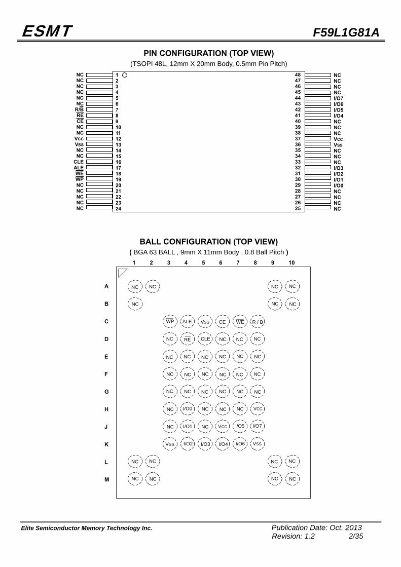
PIN CONFIGURATION (TOP VIEW)
(TSOPI 48L, 12mm X 20mm Body, 0.5mm Pin Pitch)
123456789101112131415161718192021222324
NCNCNCNCNCNC
R/BRECENCNC
VCCVSSNCNC
CLEALEWEWPNCNCNCNCNC
484746454443424140393837363534333231302928272625
NCNCNCNCI/O7I/O6I/O5I/O4NCNCNCVCCVSSNCNCNCI/O3I/O2I/O1I/O0NCNCNCNC
BALL CONFIGURATION (TOP VIEW) ( BGA 63 BALL , 9mm X 11mm Body , 0.8 Ball Pitch )
A
B
C
D
E
F
G
H
J
K
L
M
1 2 3 4 5 6 7 8 9 10
WEWP CE
RE
ALE R / BVSS
VSSVSS
VCC
VCC
I/O0
I/O1
I/O2 I/O3 I/O4 I/O6
I/O5 I/O7
NC NC
NC NC
NC NC
NC
NC NC
NC NC
NC NC
NC NC
NC NC
NC NC
NC NC
NC NC
NC NC
NC NC
NC NC
NC NC
NC NC
NC NC
NC NC
NCNC
NC
NC NC
NC
CLE
ESMT F59L1G81A
Elite Semiconductor Memory Technology Inc. Publication Date: Oct. 2013 Revision: 1.2 3/35
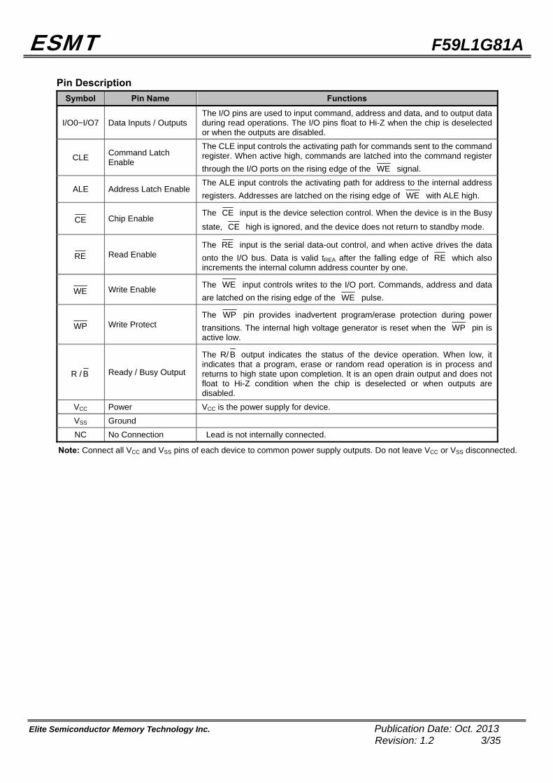
Pin Description
Symbol Pin Name Functions
I/O0~I/O7 Data Inputs / Outputs The I/O pins are used to input command, address and data, and to output data during read operations. The I/O pins float to Hi-Z when the chip is deselected or when the outputs are disabled.
CLE Command Latch Enable
The CLE input controls the activating path for commands sent to the command register. When active high, commands are latched into the command register through the I/O ports on the rising edge of the WE signal.
ALE Address Latch Enable The ALE input controls the activating path for address to the internal address registers. Addresses are latched on the rising edge of WE with ALE high.
CE Chip Enable The CE input is the device selection control. When the device is in the Busy
state, CE high is ignored, and the device does not return to standby mode.
RE Read Enable The RE input is the serial data-out control, and when active drives the data onto the I/O bus. Data is valid tREA after the falling edge of RE which also increments the internal column address counter by one.
WE Write Enable The WE input controls writes to the I/O port. Commands, address and data are latched on the rising edge of the WE pulse.
WP Write Protect The WP pin provides inadvertent program/erase protection during power transitions. The internal high voltage generator is reset when the WP pin is active low.
R / B Ready / Busy Output
The R/ B output indicates the status of the device operation. When low, it indicates that a program, erase or random read operation is in process and returns to high state upon completion. It is an open drain output and does not float to Hi-Z condition when the chip is deselected or when outputs are disabled.
VCC Power VCC is the power supply for device. VSS Ground NC No Connection Lead is not internally connected.
Note: Connect all VCC and VSS pins of each device to common power supply outputs. Do not leave VCC or VSS disconnected.
ESMT F59L1G81A
Elite Semiconductor Memory Technology Inc. Publication Date: Oct. 2013 Revision: 1.2 4/35
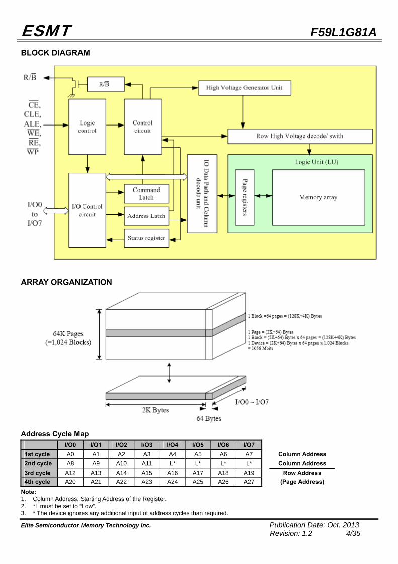
BLOCK DIAGRAM
ARRAY ORGANIZATION
Address Cycle Map
I/O0 I/O1 I/O2 I/O3 I/O4 I/O5 I/O6 I/O7 1st cycle A0 A1 A2 A3 A4 A5 A6 A7 Column Address 2nd cycle A8 A9 A10 A11 L* L* L* L* Column Address 3rd cycle A12 A13 A14 A15 A16 A17 A18 A19 Row Address 4th cycle A20 A21 A22 A23 A24 A25 A26 A27 (Page Address)
Note: 1. Column Address: Starting Address of the Register. 2. *L must be set to “Low”. 3. * The device ignores any additional input of address cycles than required.

ESMT F59L1G81A
Elite Semiconductor Memory Technology Inc. Publication Date: Oct. 2013 Revision: 1.2 5/35
Product Introduction This device is a 1,056Mbits (1,107,296,256 bits) memory organized as 65,539 rows (pages) by 2,112-byte columns. Spare 64-byte columns are located from column address of 2,048 to 2,111. A 2,112-byte data register and 2,112-byte cache register are serially connected to each other. Those serially connected registers are connected to memory cell arrays for accommodating data transfer between the I/O buffers and memory cells during page read and page program operations. The memory array is made up of 32 cells that are serially connected to form a NAND structure. Each of the 32 cells resides in a different page. A block consists of two NAND structured strings. A NAND structure consists of 32 cells. Total 1,081,344 NAND cells reside in a block. The program and read operations are executed on a page basis, while the erase operation is executed on a block basis. The memory array consists of 1,024 separately erasable 128K-byte blocks. It indicates that the bit by bit erase operation is prohibited on the device. This device uses addresses multiplexed scheme. This scheme dramatically reduces pin counts and allows systems upgrades to future densities by maintaining consistency in system board design. Command, address and data are all written through I/O's by bringing WE to low while CE is low. Those are latched on the rising edge of WE . Command Latch Enable (CLE) and Address Latch Enable (ALE) are used to multiplex command and address respectively, via the I/O pins. Some commands require one bus cycle. For example, Reset Command, Status Read Command, etc require just one cycle bus. Some other commands, like page read and block erase and page program, require two cycles: one cycle for setup and the other cycle for execution. The total physical space requires 28 addresses, thereby requiring four cycles for addressing: 2 cycle of column address, 2 cycles of row address, in that order. Page Read and Page Program need the same four address cycles following the required command input. In Block Erase operation, however, only the 2 cycles of row address are used. Device operations are selected by writing specific commands into the command register. Below table defines the specific commands of this device. The device provides cache program in a block. It is possible to write data into the cache registers while data stored in data registers are being programmed into memory cells in cache program mode. The program performance may be dramatically improved by cache program when there are lots of pages of data to be programmed. In addition to the enhanced architecture and interface, the device incorporates copy-back program feature from one page to another page without need for transporting the data to and from the external buffer memory. Since the time-consuming serial access and data-input cycles are removed, system performance for solid-state disk application is significantly increased.
Command Set
Function 1st Cycle 2nd Cycle Acceptable Command during Busy
Read 00h 30h Read for Copy Back 00h 35h Read ID 90h - Reset FFh - O Page Program 80h 10h Cache Program 80h 15h Copy-Back Program 85h 10h Block Erase 60h D0h Random Data Input(1) 85h - Random Data Output(1) 05h E0h Read Status 70h - O
Note: 1. Random Data Input / Output can be executed in a page.
Caution: Any undefined command inputs are prohibited except for above command set of above table.

ESMT F59L1G81A
Elite Semiconductor Memory Technology Inc. Publication Date: Oct. 2013 Revision: 1.2 6/35
ABSOLUTE MAXIMUM RATINGS
Parameter Symbol Rating Unit VCC -0.6 to +4.6 VIN Voltage on any pin relative to VSS VI/O -0.6 to VCC + 0.3 (< 4.6)
V
Temperature Under Bias TBIAS -10 to +125 ℃ Storage Temperature TSTG -65 to +150 ℃ Short Circuit Current IOS 5 mA
Note: 1. Minimum DC voltage is -0.6V on input/output pins. During transitions, this level may undershoot to -2.0V for periods <30ns.
Maximum DC voltage on input/output pins is VCC+0.3V which, during transitions, may overshoot to VCC+2.0V for periods <20ns. 2. Permanent device damage may occur if ABSOLUTE MAXIMUM RATINGS are exceeded. Functional operation should be
restricted to the conditions as detailed in the operational sections of this data sheet. Exposure to absolute maximum rating conditions for extended periods may affect reliability.
RECOMMENDED OPERATING CONDITIONS (Voltage reference to GND, TA = 0 to 70 )℃
Parameter Symbol Min. Typ. Max. Unit Supply Voltage VCC 2.6 3.3 3.6 V Supply Voltage VSS 0 0 0 V
DC AND OPERATION CHARACTERISTICS (Recommended operating conditions otherwise noted)
Parameter Symbol Test Conditions Min. Typ. Max. Unit
Sequential Read ICC1 tRC=25ns, CE =VIL, IOUT=0mA - 15 30
Program ICC2 - - 15 30 Operating Current
Erase ICC3 - - 15 30
mA
Stand-by Current (TTL) ISB1 CE =VIH, WP =0V/VCC - - 1 mA
Stand-by Current (CMOS) ISB2 CE = VCC -0.2, WP =0V/ VCC - 10 50 uA
Input Leakage Current ILI VIN=0 to VCC (max) - - ±10 uAOutput Leakage Current ILO VOUT=0 to VCC (max) - - ±10 uAInput High Voltage VIH - 0.8 x VCC - VCC +0.3 V Input Low Voltage, All inputs VIL - -0.3 - 0.2 x VCC V Output High Voltage Level VOH IOH=-400uA 2.4 - - V Output Low Voltage Level VOL IOL=2.1mA - - 0.4 V Output Low Current (R/B) IOL (R / B ) VOL=0.4V 8 10 - mA
Note: 1. VIL can undershoot to -0.4V and VIH can overshoot to VCC+0.4V for durations of 20ns or less. 2. Typical value are measured at VCC =3.3V, TA=25 . And not 100% tested.℃ VALID BLOCK
Symbol Min. Typ. Max. Unit NVB 1,004 - 1,024 Blocks
Note: 1. The device may include initial invalid blocks when first shipped. Additional invalid blocks may develop while being used. The
number of valid blocks is presented as first shipped. Invalid blocks are defined as blocks that contain one or more bad bits which cause status failure during program and erase operation. Do not erase or program factory-marked bad blocks. Refer to the attached technical notes for appropriate management of initial invalid blocks.
2. The 1st block, which is placed on 00h block address, is guaranteed to be a valid block up to 1K program/erase cycles with 1 bit/528 bytes ECC.
ESMT F59L1G81A
Elite Semiconductor Memory Technology Inc. Publication Date: Oct. 2013 Revision: 1.2 7/35
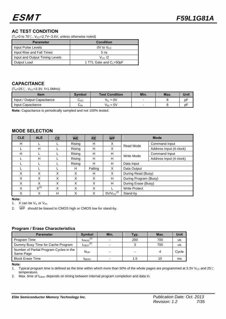
AC TEST CONDITION (TA=0 to 70 , V℃ CC=2.7V~3.6V, unless otherwise noted)
Parameter Condition Input Pulse Levels 0V to VCC Input Rise and Fall Times 5 ns Input and Output Timing Levels VCC /2 Output Load 1 TTL Gate and CL=50pF
CAPACITANCE (TA=25 , V℃ CC=3.3V, f=1.0MHz)
Item Symbol Test Condition Min. Max. UnitInput / Output Capacitance CI/O VIL = 0V - 8 pF Input Capacitance CIN VIN = 0V - 8 pF
Note: Capacitance is periodically sampled and not 100% tested. MODE SELECTION
CLE ALE CE WE RE WP Mode
H L L Rising H X Command Input L H L Rising H X
Read Mode Address Input (4 clock)
H L L Rising H H Command Input L H L Rising H H
Write Mode Address Input (4 clock)
L L L Rising H H Data Input L L L H Falling X Data Output X X X X H X During Read (Busy) X X X X X H During Program (Busy) X X X X X H During Erase (Busy) X X(1) X X X L Write Protect X X H X X 0V/VCC
(2) Stand-by
Note: 1. X can be VIL or VIH. 2. WP should be biased to CMOS high or CMOS low for stand-by. Program / Erase Characteristics
Parameter Symbol Min. Typ. Max. Unit Program Time tPROG
(1) - 200 700 us Dummy Busy Time for Cache Program tCBSY
(2) - 3 700 us Number of Partial Program Cycles in the Same Page NOP - - 4 Cycle
Block Erase Time tBERS - 1.5 10 ms
Note: 1. Typical program time is defined as the time within which more than 50% of the whole pages are programmed at 3.3V VCC and 25 ℃
temperature. 2. Max. time of tCBSY depends on timing between internal program completion and data in.
ESMT F59L1G81A
Elite Semiconductor Memory Technology Inc. Publication Date: Oct. 2013 Revision: 1.2 8/35
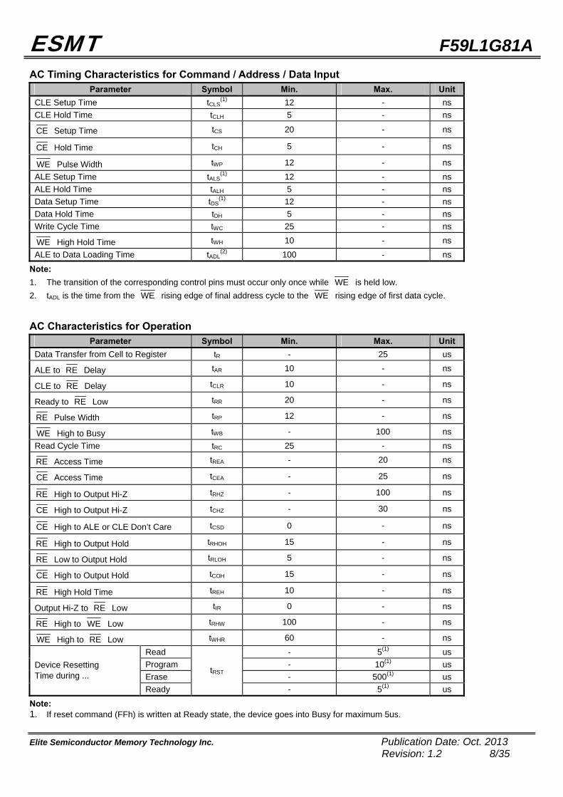
AC Timing Characteristics for Command / Address / Data Input
Parameter Symbol Min. Max. Unit CLE Setup Time tCLS
(1) 12 - ns CLE Hold Time tCLH 5 - ns CE Setup Time tCS 20 - ns CE Hold Time tCH 5 - ns WE Pulse Width tWP 12 - ns ALE Setup Time tALS
(1) 12 - ns ALE Hold Time tALH 5 - ns Data Setup Time tDS
(1) 12 - ns Data Hold Time tDH 5 - ns Write Cycle Time tWC 25 - ns WE High Hold Time tWH 10 - ns ALE to Data Loading Time tADL
(2) 100 - ns Note: 1. The transition of the corresponding control pins must occur only once while WE is held low. 2. tADL is the time from the WE rising edge of final address cycle to the WE rising edge of first data cycle. AC Characteristics for Operation
Parameter Symbol Min. Max. Unit Data Transfer from Cell to Register tR - 25 us
ALE to RE Delay tAR 10 - ns CLE to RE Delay tCLR 10 - ns Ready to RE Low tRR 20 - ns RE Pulse Width tRP 12 - ns WE High to Busy tWB - 100 ns Read Cycle Time tRC 25 - ns RE Access Time tREA - 20 ns CE Access Time tCEA - 25 ns RE High to Output Hi-Z tRHZ - 100 ns CE High to Output Hi-Z tCHZ - 30 ns CE High to ALE or CLE Don’t Care tCSD 0 - ns RE High to Output Hold tRHOH 15 - ns RE Low to Output Hold tRLOH 5 - ns CE High to Output Hold tCOH 15 - ns RE High Hold Time tREH 10 - ns Output Hi-Z to RE Low tIR 0 - ns RE High to WE Low tRHW 100 - ns WE High to RE Low tWHR 60 - ns
Read - 5(1) us Program - 10(1) us Erase - 500(1) us
Device Resetting Time during ...
Ready
tRST
- 5(1) us
Note: 1. If reset command (FFh) is written at Ready state, the device goes into Busy for maximum 5us.
ESMT F59L1G81A
Elite Semiconductor Memory Technology Inc. Publication Date: Oct. 2013 Revision: 1.2 9/35
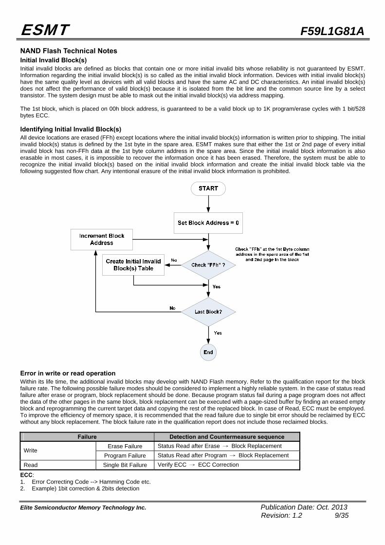
NAND Flash Technical Notes Initial Invalid Block(s) Initial invalid blocks are defined as blocks that contain one or more initial invalid bits whose reliability is not guaranteed by ESMT. Information regarding the initial invalid block(s) is so called as the initial invalid block information. Devices with initial invalid block(s) have the same quality level as devices with all valid blocks and have the same AC and DC characteristics. An initial invalid block(s) does not affect the performance of valid block(s) because it is isolated from the bit line and the common source line by a select transistor. The system design must be able to mask out the initial invalid block(s) via address mapping. The 1st block, which is placed on 00h block address, is guaranteed to be a valid block up to 1K program/erase cycles with 1 bit/528 bytes ECC. Identifying Initial Invalid Block(s) All device locations are erased (FFh) except locations where the initial invalid block(s) information is written prior to shipping. The initial invalid block(s) status is defined by the 1st byte in the spare area. ESMT makes sure that either the 1st or 2nd page of every initial invalid block has non-FFh data at the 1st byte column address in the spare area. Since the initial invalid block information is also erasable in most cases, it is impossible to recover the information once it has been erased. Therefore, the system must be able to recognize the initial invalid block(s) based on the initial invalid block information and create the initial invalid block table via the following suggested flow chart. Any intentional erasure of the initial invalid block information is prohibited.
Error in write or read operation Within its life time, the additional invalid blocks may develop with NAND Flash memory. Refer to the qualification report for the block failure rate. The following possible failure modes should be considered to implement a highly reliable system. In the case of status read failure after erase or program, block replacement should be done. Because program status fail during a page program does not affect the data of the other pages in the same block, block replacement can be executed with a page-sized buffer by finding an erased empty block and reprogramming the current target data and copying the rest of the replaced block. In case of Read, ECC must be employed. To improve the efficiency of memory space, it is recommended that the read failure due to single bit error should be reclaimed by ECC without any block replacement. The block failure rate in the qualification report does not include those reclaimed blocks.
Failure Detection and Countermeasure sequence Erase Failure Status Read after Erase → Block Replacement
Write Program Failure Status Read after Program → Block Replacement
Read Single Bit Failure Verify ECC → ECC Correction
ECC: 1. Error Correcting Code --> Hamming Code etc. 2. Example) 1bit correction & 2bits detection

ESMT F59L1G81A
Elite Semiconductor Memory Technology Inc. Publication Date: Oct. 2013 Revision: 1.2 10/35
Program Flow Chart Erase Flow Chart
ESMT F59L1G81A
Elite Semiconductor Memory Technology Inc. Publication Date: Oct. 2013 Revision: 1.2 11/35
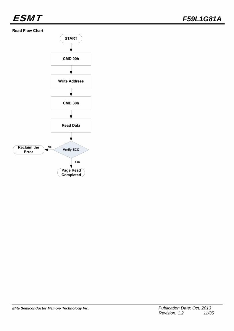
Read Flow Chart
START
CMD 00h
Write Address
CMD 30h
Read Data
No
Page Read Completed
Verify ECCReclaim the Error
Yes
ESMT F59L1G81A
Elite Semiconductor Memory Technology Inc. Publication Date: Oct. 2013 Revision: 1.2 12/35
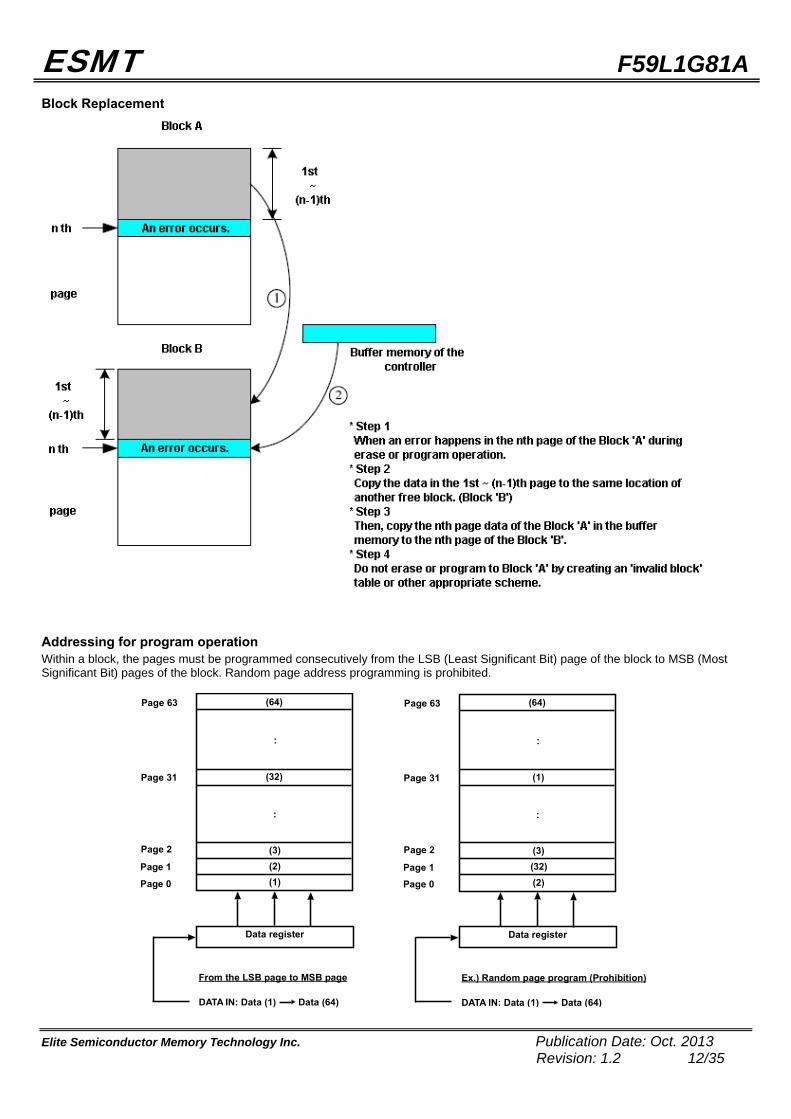
Block Replacement
Addressing for program operation Within a block, the pages must be programmed consecutively from the LSB (Least Significant Bit) page of the block to MSB (Most Significant Bit) pages of the block. Random page address programming is prohibited.
(64)
(32)
(3)(2)(1)
:
:
Page 63
Page 31
Page 2
Page 1
Page 0
Data register
From the LSB page to MSB page
DATA IN: Data (1) Data (64)
(64)
(1)
(3)(32)(2)
:
:
Page 63
Page 31
Page 2
Page 1
Page 0
Data register
Ex.) Random page program (Prohibition)
DATA IN: Data (1) Data (64)
ESMT F59L1G81A
Elite Semiconductor Memory Technology Inc. Publication Date: Oct. 2013 Revision: 1.2 13/35
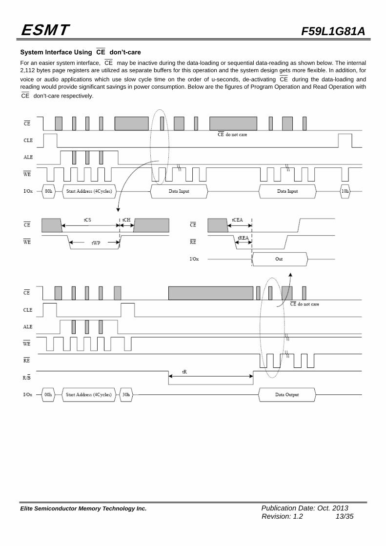
System Interface Using CE don’t-care For an easier system interface, CE may be inactive during the data-loading or sequential data-reading as shown below. The internal 2,112 bytes page registers are utilized as separate buffers for this operation and the system design gets more flexible. In addition, for voice or audio applications which use slow cycle time on the order of u-seconds, de-activating CE during the data-loading and reading would provide significant savings in power consumption. Below are the figures of Program Operation and Read Operation with CE don’t-care respectively.
ESMT F59L1G81A
Elite Semiconductor Memory Technology Inc. Publication Date: Oct. 2013 Revision: 1.2 14/35
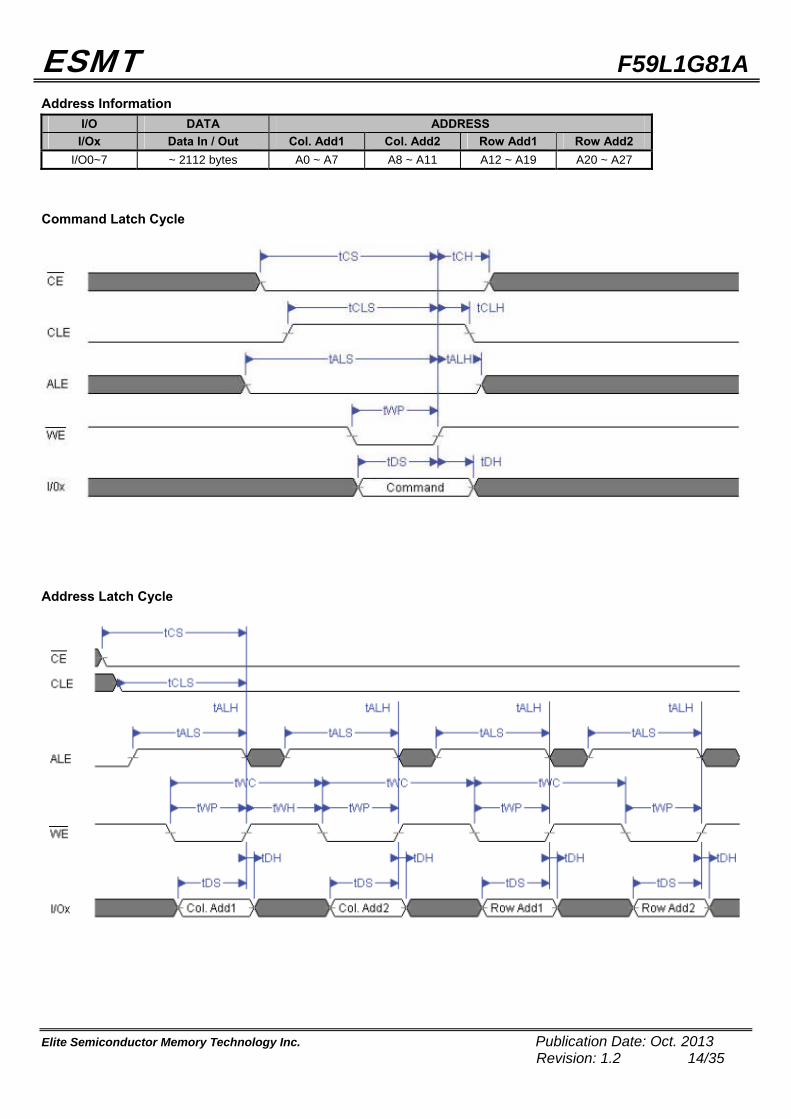
Address Information
I/O DATA ADDRESS I/Ox Data In / Out Col. Add1 Col. Add2 Row Add1 Row Add2
I/O0~7 ~ 2112 bytes A0 ~ A7 A8 ~ A11 A12 ~ A19 A20 ~ A27 Command Latch Cycle
Address Latch Cycle
ESMT F59L1G81A
Elite Semiconductor Memory Technology Inc. Publication Date: Oct. 2013 Revision: 1.2 15/35
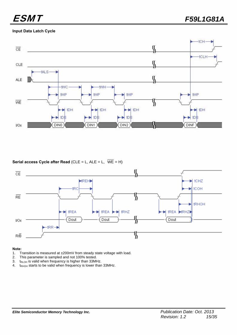
Input Data Latch Cycle
Serial access Cycle after Read (CLE = L, ALE = L, WE = H)
Note: 1. Transition is measured at ±200mV from steady state voltage with load. 2. This parameter is sampled and not 100% tested. 3. tRLOH is valid when frequency is higher than 33MHz. 4. tRHOH starts to be valid when frequency is lower than 33MHz.
ESMT F59L1G81A
Elite Semiconductor Memory Technology Inc. Publication Date: Oct. 2013 Revision: 1.2 16/35
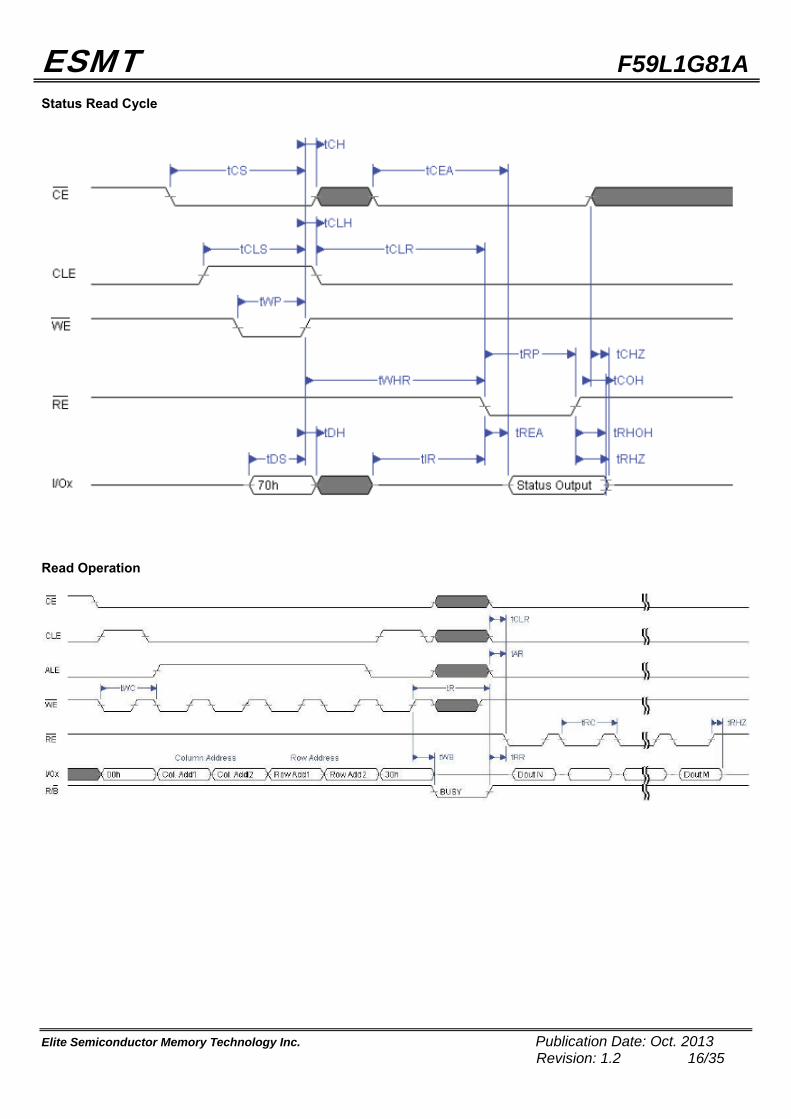
Status Read Cycle
Read Operation

ESMT F59L1G81A
Elite Semiconductor Memory Technology Inc. Publication Date: Oct. 2013 Revision: 1.2 17/35
Read Operation (Intercepted by CE )
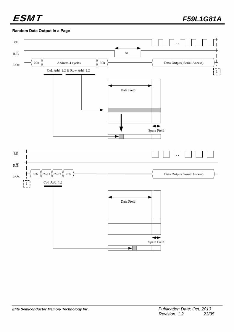
Random Data Output In a Page
ESMT F59L1G81A
Elite Semiconductor Memory Technology Inc. Publication Date: Oct. 2013 Revision: 1.2 18/35
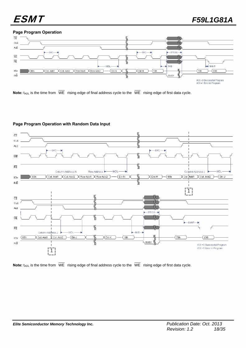
Page Program Operation
Note: tADL is the time from WE rising edge of final address cycle to the WE rising edge of first data cycle. Page Program Operation with Random Data Input
Note: tADL is the time from WE rising edge of final address cycle to the WE rising edge of first data cycle.
ESMT F59L1G81A
Elite Semiconductor Memory Technology Inc. Publication Date: Oct. 2013 Revision: 1.2 19/35
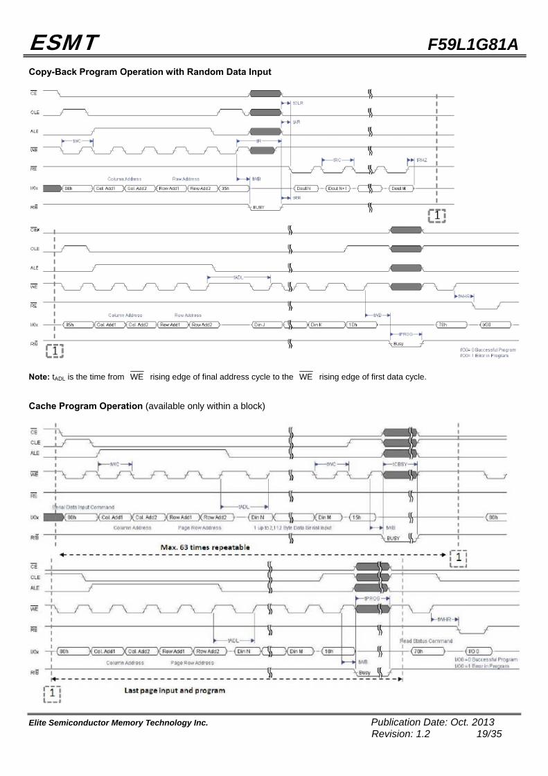
Copy-Back Program Operation with Random Data Input
Note: tADL is the time from WE rising edge of final address cycle to the WE rising edge of first data cycle. Cache Program Operation (available only within a block)
ESMT F59L1G81A
Elite Semiconductor Memory Technology Inc. Publication Date: Oct. 2013 Revision: 1.2 20/35
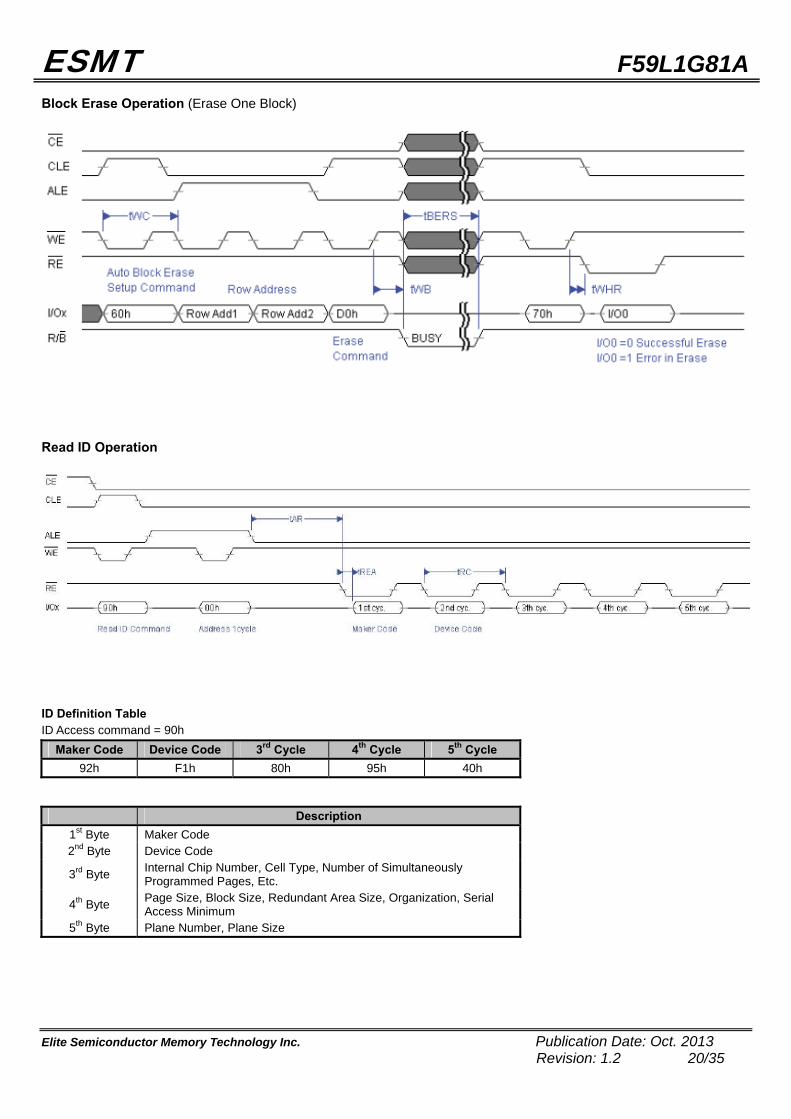
Block Erase Operation (Erase One Block)
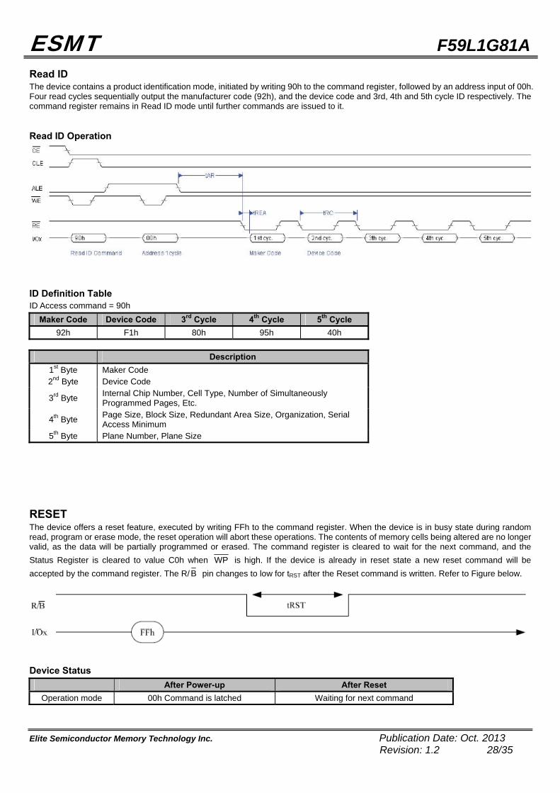
Read ID Operation
ID Definition Table ID Access command = 90h
Maker Code Device Code 3rd Cycle 4th Cycle 5th Cycle 92h F1h 80h 95h 40h
Description 1st Byte Maker Code 2nd Byte Device Code
3rd Byte Internal Chip Number, Cell Type, Number of Simultaneously Programmed Pages, Etc.
4th Byte Page Size, Block Size, Redundant Area Size, Organization, Serial Access Minimum
5th Byte Plane Number, Plane Size
ESMT F59L1G81A
Elite Semiconductor Memory Technology Inc. Publication Date: Oct. 2013 Revision: 1.2 21/35
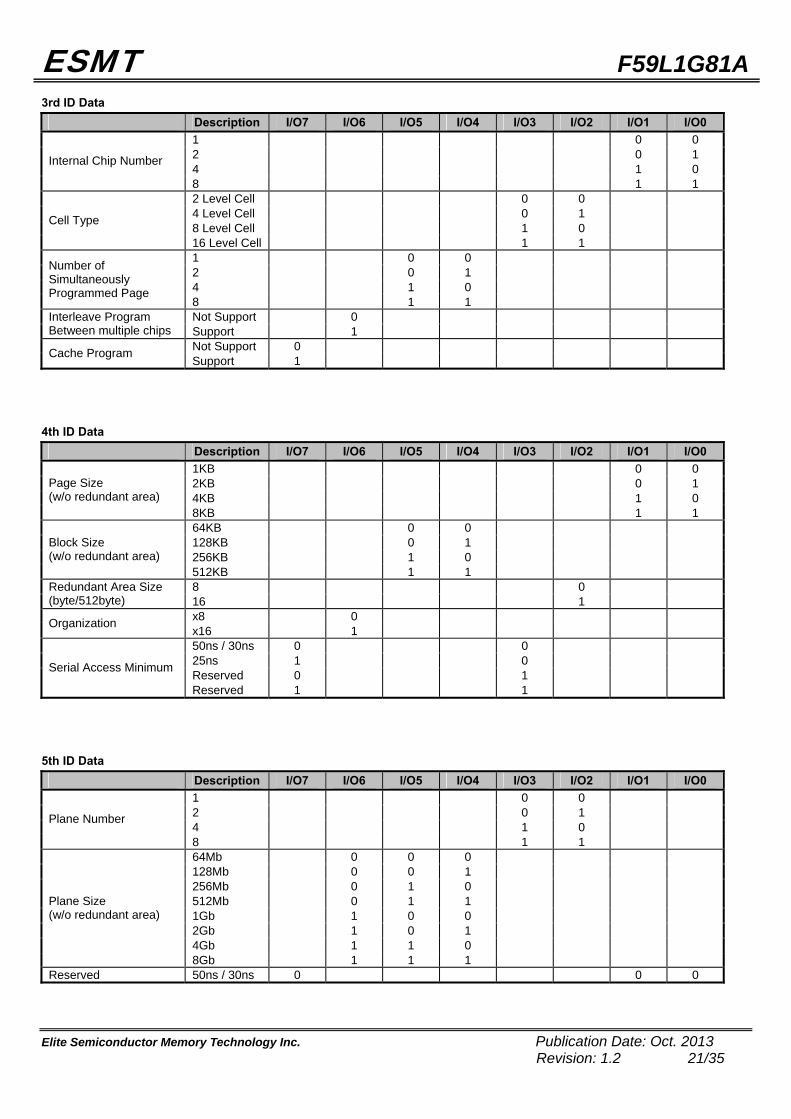
3rd ID Data
Description I/O7 I/O6 I/O5 I/O4 I/O3 I/O2 I/O1 I/O0 1 0 0 2 0 1 4 1 0
Internal Chip Number
8 1 1 2 Level Cell 0 0 4 Level Cell 0 1 8 Level Cell 1 0 Cell Type
16 Level Cell 1 1 1 0 0 2 0 1 4 1 0
Number of Simultaneously Programmed Page
8 1 1 Not Support 0 Interleave Program
Between multiple chips Support 1 Not Support 0 Cache Program Support 1
4th ID Data
Description I/O7 I/O6 I/O5 I/O4 I/O3 I/O2 I/O1 I/O0 1KB 0 0 2KB 0 1 4KB 1 0
Page Size (w/o redundant area)
8KB 1 1 64KB 0 0 128KB 0 1 256KB 1 0
Block Size (w/o redundant area)
512KB 1 1 8 0 Redundant Area Size
(byte/512byte) 16 1 x8 0 Organization x16 1 50ns / 30ns 0 0 25ns 1 0 Reserved 0 1 Serial Access Minimum
Reserved 1 1 5th ID Data
Description I/O7 I/O6 I/O5 I/O4 I/O3 I/O2 I/O1 I/O0 1 0 0 2 0 1 4 1 0
Plane Number
8 1 1 64Mb 0 0 0 128Mb 0 0 1 256Mb 0 1 0 512Mb 0 1 1 1Gb 1 0 0 2Gb 1 0 1 4Gb 1 1 0
Plane Size (w/o redundant area)
8Gb 1 1 1 Reserved 50ns / 30ns 0 0 0

ESMT F59L1G81A
Elite Semiconductor Memory Technology Inc. Publication Date: Oct. 2013 Revision: 1.2 22/35
DEVICE OPERATION Page Read Page read is initiated by writing 00h-30h to the command register along with four address cycles. After initial power up, 00h command is latched. Therefore only four address cycles and 30h command initiates that operation after initial power up. The 2,112 bytes of data within the selected page are transferred to the data registers in less than tR. The system controller can detect the completion of this data transfer (tR) by analyzing the output of R/ B pin. Once the data in a page is loaded into the data registers, they may be read out in 25ns cycle time by sequentially pulsing RE . The repetitive high to low transitions of the RE clock make the device output the data starting from the selected column address up to the last column address. The device may output random data in a page instead of the consecutive sequential data by writing random data output command. The column address of next data, which is going to be out, may be changed to the address which follows random data output command. Random data output can be operated multiple times regardless of how many times it is done in a page. Read Operation
ESMT F59L1G81A
Elite Semiconductor Memory Technology Inc. Publication Date: Oct. 2013 Revision: 1.2 23/35
Random Data Output In a Page

ESMT F59L1G81A
Elite Semiconductor Memory Technology Inc. Publication Date: Oct. 2013 Revision: 1.2 24/35
Page Program The device is programmed basically on a page basis, but it does allow multiple partial page programming of a word or consecutive bytes up to 2,112, in a single page program cycle. The number of consecutive partial page programming operation within the same page without an intervening erase operation must not exceed 4 times for a single page. The addressing should be done in sequential order in a block. A page program cycle consists of a serial data loading period in which up to 2,112 bytes of data may be loaded into the data register, followed by a non-volatile programming period where the loaded data is programmed into the appropriate cell. The serial data loading period begins by inputting the Serial Data Input command (80h), followed by the four cycle address inputs and then serial data loading. The words other than those to be programmed do not need to be loaded. The device supports random data input in a page. The column address for the next data, which will be entered, may be changed to the address which follows random data input command (85h). Random data input may be operated multiple times regardless of how many times it is done in a page. The Page Program confirm command (10h) initiates the programming process. Writing 10h alone without previously entering the serial data will not initiate the programming process. The internal write state controller automatically executes the algorithms and timings necessary for program and verify, thereby freeing the system controller for other tasks. Once the program process starts, the Read Status Register command may be entered, with RE and CE low, to read the status register. The system controller can detect the
completion of a program cycle by monitoring the R/ B output, or the Status bit (I/O6) of the Status Register. Only the Read Status command and Reset command are valid while programming is in progress. When the Page Program is complete, the Write Status Bit (I/O0) may be checked. The internal write verify detects only errors for "1"s that are not successfully programmed to "0"s. The command register remains in Read Status command mode until another valid command is written to the command register. Program & Read Status Operation
Random Data Input In a page

ESMT F59L1G81A
Elite Semiconductor Memory Technology Inc. Publication Date: Oct. 2013 Revision: 1.2 25/35
Cache Program Cache Program is an extension of Page Program, which is executed with 2,112 byte data registers, and is available only within a block. Since the device has 1 page of cache memory, serial data input may be executed while data stored in data register are programmed into memory cell. After writing the first set of data up to 2,112 bytes into the selected cache registers, Cache Program command (15h) instead of actual Page Program (10h) is inputted to make cache registers free and to start internal program operation. To transfer data from cache registers to data registers, the device remains in Busy state for a short period of time (tCBSY) and has its cache registers ready for the next data-input while the internal programming gets started with the data loaded into data registers. Read Status command (70h) may be issued to find out when cache registers become ready by polling the Cache-Busy status bit (I/O6). Pass/fail status of only the previous page is available upon the return to Ready state. When the next set of data is inputted with the Cache Program command, tCBSY is affected by the progress of pending internal programming. The programming of the cache registers is initiated only when the pending program cycle is finished and the data registers are available for the transfer of data from cache registers. The status bit (I/O5) for internal Ready/Busy may be polled to identity the completion of internal programming. If the system monitors the progress of programming only with R/ B , the last page of the target programming sequence must be programmed with actual Page Program command (10h). Cache Program (available only within a block)
Note: 1. Since programming the last page does not employ caching, the program time has to be that of Page Program. However, if the
previous program cycle with the cache data has not finished, the actual program cycle of the last page is initiated only after completion of the previous cycle, which can be expressed as the following formula.
2. tPROG = Program time for the last page + Program time for the (last-1)th page – (Program command cycle time + Last page data loading time)
ESMT F59L1G81A
Elite Semiconductor Memory Technology Inc. Publication Date: Oct. 2013 Revision: 1.2 26/35
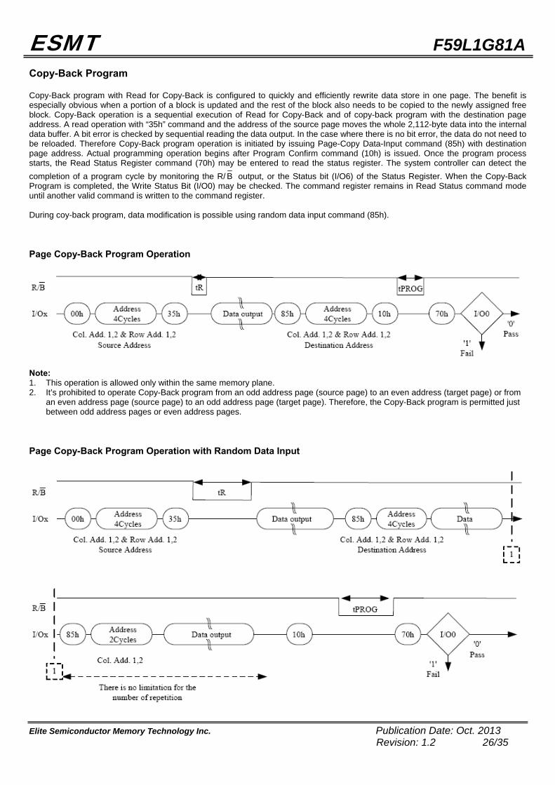
Copy-Back Program Copy-Back program with Read for Copy-Back is configured to quickly and efficiently rewrite data store in one page. The benefit is especially obvious when a portion of a block is updated and the rest of the block also needs to be copied to the newly assigned free block. Copy-Back operation is a sequential execution of Read for Copy-Back and of copy-back program with the destination page address. A read operation with “35h” command and the address of the source page moves the whole 2,112-byte data into the internal data buffer. A bit error is checked by sequential reading the data output. In the case where there is no bit error, the data do not need to be reloaded. Therefore Copy-Back program operation is initiated by issuing Page-Copy Data-Input command (85h) with destination page address. Actual programming operation begins after Program Confirm command (10h) is issued. Once the program process starts, the Read Status Register command (70h) may be entered to read the status register. The system controller can detect the completion of a program cycle by monitoring the R/ B output, or the Status bit (I/O6) of the Status Register. When the Copy-Back Program is completed, the Write Status Bit (I/O0) may be checked. The command register remains in Read Status command mode until another valid command is written to the command register. During coy-back program, data modification is possible using random data input command (85h). Page Copy-Back Program Operation
Note: 1. This operation is allowed only within the same memory plane. 2. It’s prohibited to operate Copy-Back program from an odd address page (source page) to an even address (target page) or from
an even address page (source page) to an odd address page (target page). Therefore, the Copy-Back program is permitted just between odd address pages or even address pages.
Page Copy-Back Program Operation with Random Data Input

ESMT F59L1G81A
Elite Semiconductor Memory Technology Inc. Publication Date: Oct. 2013 Revision: 1.2 27/35
Block Erase The Erase operation is done on a block basis. Block address loading is accomplished in two cycles initiated by an Erase Setup command (60h). Only address A18 to A27 is valid while A12 to A17 is ignored. The Erase Confirm command (D0h) following the block address loading initiates the internal erasing process. This two-step sequence of setup followed by execution command ensures that memory contents are not accidentally erased due to external noise conditions. At the rising edge of WE after the erase confirm command input, the internal write controller handles erase and erase-verify. When the erase operation is completed, the Write Status Bit (I/O0) may be checked. Block Erase Operation
Read Status The device contains a Status Register which may be read to find out whether program or erase operation is completed, and whether the program or erase operation is completed successfully. After writing 70h command to the command register, a read cycle outputs the content of the Status Register to the I/O pins on the falling edge of CE or RE , whichever occurs last. This two line control allows
the system to poll the progress of each device in multiple memory connections even when R/ B pins are common-wired. RE or CE does not need to be toggled for updated status. Refer to below table for specific Status Register definitions. The command register remains in Status Read mode until further commands are issued to it. Therefore, if the status register is read during a random read cycle, the read command (00h) should be given before starting read cycles. Status Register Definition for 70h Command
I/O Page Block Cache Read Definition I/O0 Pass / Fail Pass / Fail Pass / Fail(N) Not Use Pass: ”0” Fail: ”1” I/O1 Not Use Not Use Pass / Fail(N-1) Not Use Pass: ”0” Fail: ”1” I/O2 Not Use Not Use Not Use Not Use Don’t cared I/O3 Not Use Not Use Not Use Not Use Don’t cared I/O4 Not Use Not Use Not Use Not Use Don’t cared
I/O5 Ready / Busy Ready / Busy True Ready / Busy Ready / Busy Busy: ”0” Ready: ”1”
I/O6 Ready / Busy Ready / Busy Ready / Busy Ready / Busy Busy: ”0” Ready: ”1”
I/O7 Write Protect Write Protect Write Protect Write Protect Protected: ”0” Not Protected: ”1”
Note: 1. True Ready/Busy represents internal program operation status which is being executed in cache program mode. 2. I/Os defined ’Not Use’ are recommended to be masked out when Read Status is being executed.
ESMT F59L1G81A
Elite Semiconductor Memory Technology Inc. Publication Date: Oct. 2013 Revision: 1.2 28/35
Read ID The device contains a product identification mode, initiated by writing 90h to the command register, followed by an address input of 00h. Four read cycles sequentially output the manufacturer code (92h), and the device code and 3rd, 4th and 5th cycle ID respectively. The command register remains in Read ID mode until further commands are issued to it. Read ID Operation
ID Definition Table ID Access command = 90h
Maker Code Device Code 3rd Cycle 4th Cycle 5th Cycle 92h F1h 80h 95h 40h
Description
1st Byte Maker Code 2nd Byte Device Code
3rd Byte Internal Chip Number, Cell Type, Number of Simultaneously Programmed Pages, Etc.
4th Byte Page Size, Block Size, Redundant Area Size, Organization, Serial Access Minimum
5th Byte Plane Number, Plane Size
RESET The device offers a reset feature, executed by writing FFh to the command register. When the device is in busy state during random read, program or erase mode, the reset operation will abort these operations. The contents of memory cells being altered are no longer valid, as the data will be partially programmed or erased. The command register is cleared to wait for the next command, and the Status Register is cleared to value C0h when WP is high. If the device is already in reset state a new reset command will be accepted by the command register. The R/B pin changes to low for tRST after the Reset command is written. Refer to Figure below.
Device Status
After Power-up After Reset Operation mode 00h Command is latched Waiting for next command
ESMT F59L1G81A
Elite Semiconductor Memory Technology Inc. Publication Date: Oct. 2013 Revision: 1.2 29/35
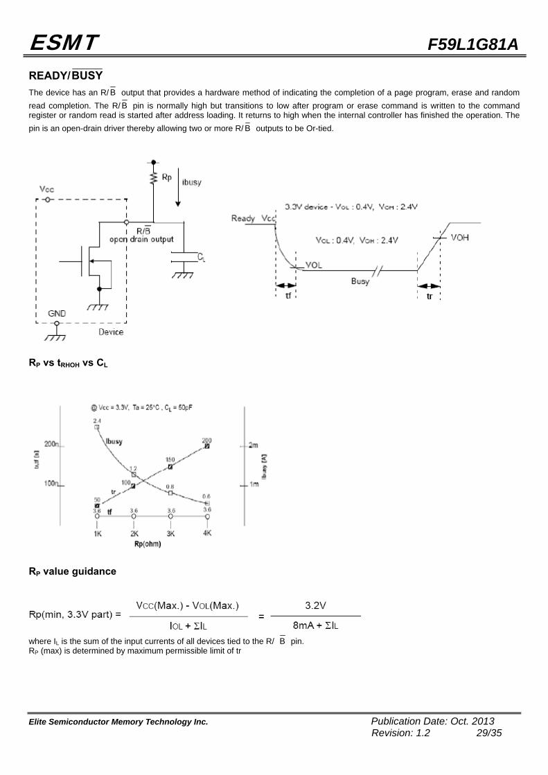
READY/BUSY The device has an R/ B output that provides a hardware method of indicating the completion of a page program, erase and random read completion. The R/ B pin is normally high but transitions to low after program or erase command is written to the command register or random read is started after address loading. It returns to high when the internal controller has finished the operation. The pin is an open-drain driver thereby allowing two or more R/ B outputs to be Or-tied.
RP vs tRHOH vs CL
RP value guidance
where IL is the sum of the input currents of all devices tied to the R/ B pin. RP (max) is determined by maximum permissible limit of tr

ESMT F59L1G81A
Elite Semiconductor Memory Technology Inc. Publication Date: Oct. 2013 Revision: 1.2 30/35
Data Protection & Power-up sequence The device is designed to offer protection from any involuntary program/erase during power-transitions. An internal voltage detector disables all functions whenever VCC is below about 2V. WP pin provides hardware protection and is recommended to be kept at VIL during power-up and power-down. A recovery time of minimum 100us is required before internal circuit gets ready for any command sequences as below. The two step command sequence for program/erase provides additional software protection. AC Waveforms for Power Transition
Note: During the initialization, the device consumes a maximum current of ICC1.
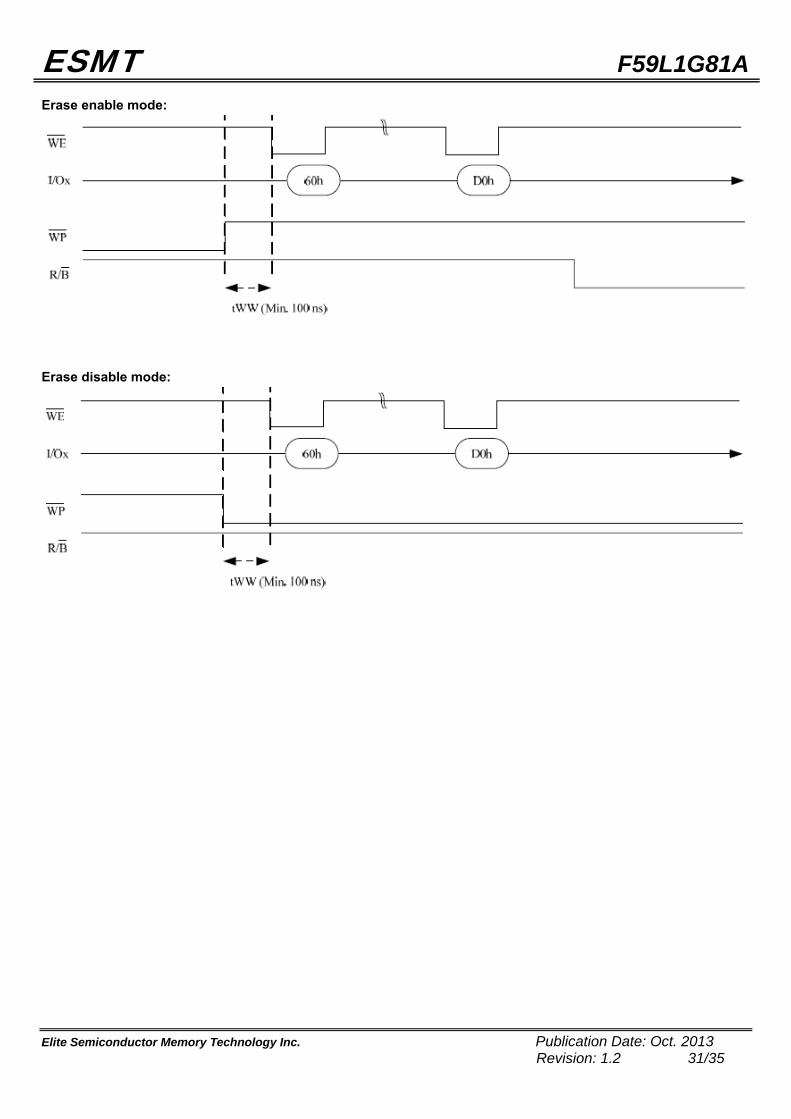
WP AC Timing guide Enable WP during erase and program busy is prohibited. The erase and program operations are enabled and disable as follows. Program enable mode:
Program disable mode:
ESMT F59L1G81A
Elite Semiconductor Memory Technology Inc. Publication Date: Oct. 2013 Revision: 1.2 31/35
Erase enable mode:
Erase disable mode:
ESMT F59L1G81A
Elite Semiconductor Memory Technology Inc. Publication Date: Oct. 2013 Revision: 1.2 32/35
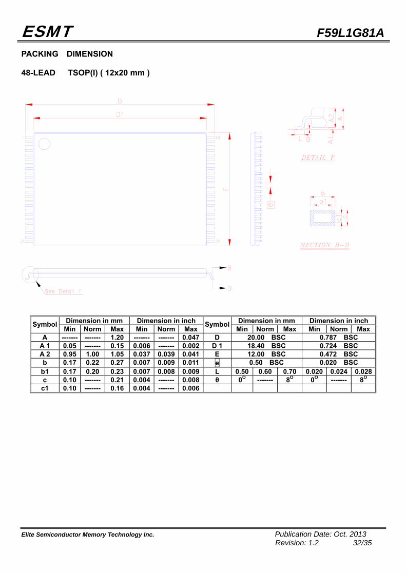
PACKING DIMENSION 48-LEAD TSOP(I) ( 12x20 mm )
Dimension in mm Dimension in inch Dimension in mm Dimension in inch Symbol Min Norm Max Min Norm Max Symbol Min Norm Max Min Norm MaxA ------- ------- 1.20 ------- ------- 0.047 D 20.00 BSC 0.787 BSC
A 1 0.05 ------- 0.15 0.006 ------- 0.002 D 1 18.40 BSC 0.724 BSC A 2 0.95 1.00 1.05 0.037 0.039 0.041 E 12.00 BSC 0.472 BSC b 0.17 0.22 0.27 0.007 0.009 0.011 e 0.50 BSC 0.020 BSC
b1 0.17 0.20 0.23 0.007 0.008 0.009 L 0.50 0.60 0.70 0.020 0.024 0.028c 0.10 ------- 0.21 0.004 ------- 0.008 θ 0O ------- 8O 0O ------- 8O c1 0.10 ------- 0.16 0.004 ------- 0.006
ESMT F59L1G81A
Elite Semiconductor Memory Technology Inc. Publication Date: Oct. 2013 Revision: 1.2 33/35
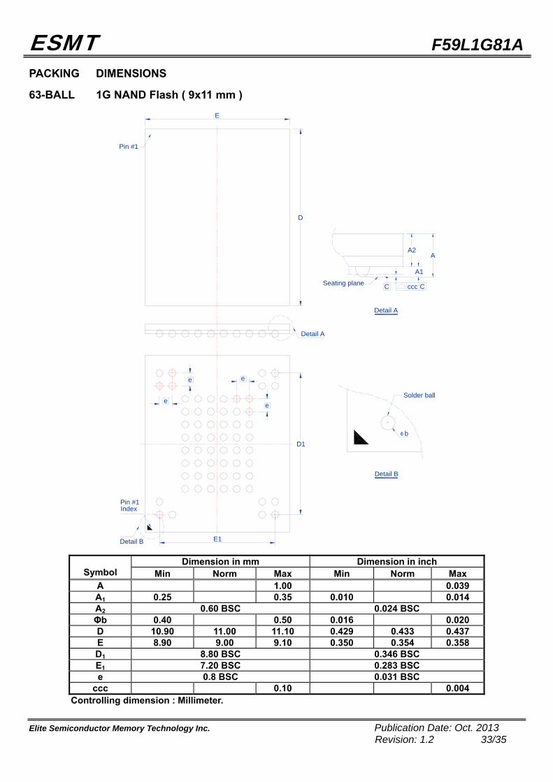
PACKING DIMENSIONS 63-BALL 1G NAND Flash ( 9x11 mm )
A2
A1
A
Seating plane C ccc
C
Solder ball
b
Pin #1
Pin #1Index
Detail B
Detail A
Detail A
Detail B
e
ee
e
D1
E1
D
E
Dimension in mm Dimension in inch
Symbol Min Norm Max Min Norm Max A 1.00 0.039 A1 0.25 0.35 0.010 0.014 A2 0.60 BSC 0.024 BSC
Φb 0.40 0.50 0.016 0.020 D 10.90 11.00 11.10 0.429 0.433 0.437 E 8.90 9.00 9.10 0.350 0.354 0.358 D1 8.80 BSC 0.346 BSC
E1 7.20 BSC 0.283 BSC
e 0.8 BSC 0.031 BSC
ccc 0.10 0.004
Controlling dimension : Millimeter.

ESMT F59L1G81A
Elite Semiconductor Memory Technology Inc. Publication Date: Oct. 2013 Revision: 1.2 34/35
Revision History
Revision Date Description
0.1 2010.11.22 Original
1.0 2011.12.27 1.Delete “Preliminary” 2.Add BGA package
1.1 2013.07.12 Delete unique ID from features
1.2 2013.10.15 Add "No Bad-Block-Erasing-Protect function"
ESMT F59L1G81A
Elite Semiconductor Memory Technology Inc. Publication Date: Oct. 2013 Revision: 1.2 35/35
Important Notice All rights reserved. No part of this document may be reproduced or duplicated in any form or by any means without the prior permission of ESMT. The contents contained in this document are believed to be accurate at the time of publication. ESMT assumes no responsibility for any error in this document, and reserves the right to change the products or specification in this document without notice. The information contained herein is presented only as a guide or examples for the application of our products. No responsibility is assumed by ESMT for any infringement of patents, copyrights, or other intellectual property rights of third parties which may result from its use. No license, either express , implied or otherwise, is granted under any patents, copyrights or other intellectual property rights of ESMT or others. Any semiconductor devices may have inherently a certain rate of failure. To minimize risks associated with customer's application, adequate design and operating safeguards against injury, damage, or loss from such failure, should be provided by the customer when making application designs. ESMT's products are not authorized for use in critical applications such as, but not limited to, life support devices or system, where failure or abnormal operation may directly affect human lives or cause physical injury or property damage. If products described here are to be used for such kinds of application, purchaser must do its own quality assurance testing appropriate to such applications.