esmt/emp preliminary ad83582 - micro bridgemicro-bridge.com/data/emp/ad83582.pdf · z short-circuit...
TRANSCRIPT

ESMT/EMP Preliminary AD83582
Elite Semiconductor Memory Technology Inc./Elite MicroPower Inc. Publication Date: Sep. 2011 Revision: 0.2 1/57
10Wx2 +20W 2.1CH Digital Audio Amplifier with EQ Functions and Sub-Woofer PWM out
Features
16/18/20/24-bits input with I2S, Left-alignment and Right-alignment data format PSNR & DR(A-weighting) Loudspeaker: 98dB (PSNR), 108dB (DR) @24V Multiple sampling frequencies (Fs) 32kHz / 44.1kHz / 48kHz and 64kHz / 88.2kHz / 96kHz and 128kHz / 176.4kHz / 192kHz System clock = 64x, 128x, 192x, 256x, 384x, 512x, 576x, 768x, 1024x Fs 64x~1024x Fs for 32kHz / 44.1kHz / 48kHz 64x~512x Fs for 64kHz / 88.2kHz / 96kHz 64x~256x Fs for 128kHz / 176.4kHz / 192kHz Supply voltage 3.3V for digital circuit 12V~24V for loudspeaker driver Loudspeaker output power for 24V 10W x 2CH into 8Ω @0.2% THD+N for stereo 15W x 2CH into 8Ω @0.25% THD+N for stereo 20W x 1CH into 4Ω @0.25% THD+N for mono 30W x 1CH into 4Ω @0.3% THD+N for mono Sound processing including: 8 bands parametric EQ Volume control (+24dB~-103dB, 0.5dB/step), Dynamic range control 3D surround sound Channel mixing Automatic Zero-detection mute Bass/Treble tone control Bass management crossover filter DC-blocking high-pass filter Anti-pop design Over-temperature protection I2C control interface with selectable device address Support hardware and software reset Internal PLL Subwoofer PWM output Under-voltage shutdown Short-circuit protection
Applications CD and DVD TV audio Car audio Boom-box MP3 docking systems Powered speaker Wireless audio
Description AD83582 is a digital audio amplifier capable of
driving a pair of 8Ω, 10W and 4Ω SE, 10W or a single 4Ω, 20W speaker operating at 24V supply without external heat-sink or fan requirement. It’s also capable of driving a pair of 8Ω, 15W or a single 4Ω, 30W speaker operating at a 24V supply with proper cooling method.
AD83582 can provide advanced audio processing
capabilities, such as volume control, 8 EQ bands, audio mixing, 3D surround and Dynamic Range Control(DRC).These functions are fully programmable via a simple I2C control interface. Robust protection circuits are provided to protect AD83582 from damage due to accidental erroneous operating condition. AD83582 is more tolerant to noise and PVT (Process, Voltage, and Temperature) variation than the analog class-AB or class-D audio amplifier counterpart implemented by analog circuit design. AD83582 is pop free during instantaneous power switch because of its built-in, robust anti-pop circuit.
The output stage is flexibly configurable for stereo or mono applications. In addition, AD83582 provides a sub-woofer PWM output port for the increasingly popular 2.1 channel applications. The programmable audio bass content of this subwoofer PWM output port can drive an external, low cost digital amplifier power stage (such as ESMT’s AD9256H, AD92580, ..). Furthermore, it is possible to use three pieces of AD83582 to realize 5.1 channels for home theater applications.

ESMT/EMP Preliminary AD83582
Elite Semiconductor Memory Technology Inc./Elite MicroPower Inc. Publication Date: Sep. 2011 Revision: 0.2 2/57
Pin Assignment
Pin Description
PIN NAME TYPE DESCRIPTION CHARACTERISTICS
1 VDDLA P Left channel supply A
2 N.C. NC
3 N.C. NC
4 N.C. NC
5 N.C. NC
6 PLL I PLL enable, low active Schmitt trigger TTL input buffer
7 MCLK I Master clock input Schmitt trigger TTL input buffer
8 CLK_OUT O Clock output from PLL TTL output buffer
9 DGND P Digital Ground
10 DVDD P Digital Power
11 DEF I Default volume setting
(1:Un-Mute ; 0:Mute) Schmitt trigger TTL input buffer
12 SDATA I Serial audio data input Schmitt trigger TTL input buffer
13 CFG0 I Stereo/Mono configuration pin
(1:Stereo ; 0: Mono) Schmitt trigger TTL input buffer

ESMT/EMP Preliminary AD83582
Elite Semiconductor Memory Technology Inc./Elite MicroPower Inc. Publication Date: Sep. 2011 Revision: 0.2 3/57
14 CFG1 I Sub-woofer PWM output enable, high
active Schmitt trigger TTL input buffer
15 LRCIN I Left/Right clock input (Fs) Schmitt trigger TTL input buffer
16 BCLK I Bit clock input (64Fs) Schmitt trigger TTL input buffer
17 PD I Power down, low active Schmitt trigger TTL input buffer
18 ERROR O Error status, low active Open-drain output
19 RESET I Reset, low active Schmitt trigger TTL input buffer
20 SA0 I I2C select address 0 Schmitt trigger TTL input buffer
21 SA1 I I2C select address 1 Schmitt trigger TTL input buffer
22 SUBA O Sub-Woofer PWM output A
23 SUBB O Sub-Woofer PWM output B
24 SCL I I2C serial clock input Schmitt trigger TTL input buffer
25 SDA I/O I2C bi-directional serial data Schmitt trigger TTL input buffer
26 DGND P Digital Ground
27 DVDD P Digital Power
28 LREX I Left/Right channel exchange Schmitt trigger TTL input buffer
29 SUB_SDATAO O Sub-woofer serial audio data output
30 N.C. NC
31 N.C. NC
32 N.C. NC
33 TEST_1 O Reserved pin for testing purpose
34 TEST_2 O Reserved pin for testing purpose
35 N.C. NC
36 VDDRA P Right channel supply A
37 RA O Right channel output A
38 N.C. NC
39 GNDRA P Right channel ground
40 GNDRB P
41 RB O Right channel output B
42 VDDRB P Right channel supply B
43 VDDLB P Left channel supply B
44 LB O Left channel output B
45 GNDLB P
46 GNDLA P Left channel ground
47 N.C. NC
48 LA O Left channel output A
ESMT/EMP Preliminary AD83582
Elite Semiconductor Memory Technology Inc./Elite MicroPower Inc. Publication Date: Sep. 2011 Revision: 0.2 4/57
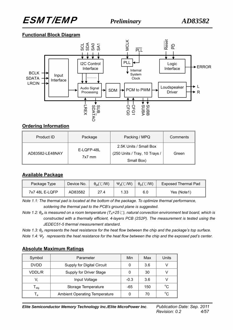
Functional Block Diagram
SA1
InputInterface
I2C ControlInterface
PCM to PWM LoudspeakerDriver
LR
BCLKSDATALRCIN
ERROR
Audio Signal Processing SDM
CFG
1
Res
et
PD
PLL
InternalSystem Clock
PLL
LogicInterface
SA0
SD
AS
CL
MC
LK
CFG
0
LRE
X
SU
BAS
UBB
SU
B_S
DATA
O
Ordering Information
Product ID Package Packing / MPQ Comments
AD83582-LE48NAY E-LQFP-48L
7x7 mm
2.5K Units / Small Box
(250 Units / Tray, 10 Trays /
Small Box)
Green
Available Package
Package Type Device No. θja( /W) Ψjt( /W) θjc( /W) Exposed Thermal Pad
7x7 48L E-LQFP AD83582 27.4 1.33 6.0 Yes (Note1)
Note 1.1: The thermal pad is located at the bottom of the package. To optimize thermal performance, soldering the thermal pad to the PCB’s ground plane is suggested.
Note 1.2: θja is measured on a room temperature (TA=25 ), natural convection environment test board, which is
constructed with a thermally efficient, 4-layers PCB (2S2P). The measurement is tested using the JEDEC51-5 thermal measurement standard.
Note 1.3: θjc represents the heat resistance for the heat flow between the chip and the package’s top surface. Note 1.4: Ψjt represents the heat resistance for the heat flow between the chip and the exposed pad’s center. Absolute Maximum Ratings
Symbol Parameter Min Max Units
DVDD Supply for Digital Circuit 0 3.6 V
VDDL/R Supply for Driver Stage 0 30 V
Vi Input Voltage -0.3 3.6 V
Tstg Storage Temperature -65 150 oC
Ta Ambient Operating Temperature 0 70 oC

ESMT/EMP Preliminary AD83582
Elite Semiconductor Memory Technology Inc./Elite MicroPower Inc. Publication Date: Sep. 2011 Revision: 0.2 5/57
Recommended Operating Conditions
Digital Characteristics
Symbol Parameter Min Typ Max Units
VIH High-Level Input Voltage 2.0 V
VIL Low-Level Input Voltage 0.8 V
VOH High-Level Output Voltage 2.4 V
VOL Low-Level Output Voltage 0.4 V
CI Input Capacitance 6.4 pF
General Electrical Characteristics
Symbol Parameter Condition Min Typ Max Units
IPD(HV) PVDD Supply Current during Power Down PVDD=24V 10 uA
IPD(LV) DVDD Supply Current during Power Down DVDD=3.3V 10 uA
Junction Temperature for Driver Shutdown 160 oCTSENSOR
Temperature Hysteresis for Recovery from Shutdown 40 oC
UVH Under Voltage Disabled (For DVDD) 2.8 V
UVL Under Voltage Enabled (For DVDD) 2.7 V
Static Drain-to-Source On-state Resistor, PMOS 295 m Rds-on
Static Drain-to-Source On-state Resistor, NMOS PVDD=24V, Id=500mA 185 m
L(R) Channel Over-Current Protection (Note 2) PVDD=24V 5 A ISC
Mono Channel Over-Circuit Protection (Note 2) PVDD=24V 10 A
Note 2: Loudspeaker over-current protection is only effective when loudspeaker drivers are properly
connected with external LC filters. Please refer to the application circuit example for recommended
LC filter configuration.
Marking Information
AD83582
Line 1 : LOGO
Line 2 : Product no.
Line 3 : Tracking Code
Line 4 : Date Code
Symbol Parameter Typ Units
DVDD Supply for Digital Circuit 3.15~3.45 V
VDDL/R Supply for Driver Stage 10~26 V
Ta Ambient Operating Temperature 0~70 oC
PIN1 DOT
ESMTAD83582Tracking Code
Date Code

ESMT/EMP Preliminary AD83582
Elite Semiconductor Memory Technology Inc./Elite MicroPower Inc. Publication Date: Sep. 2011 Revision: 0.2 6/57
Application Circuit Example for Stereo

ESMT/EMP Preliminary AD83582
Elite Semiconductor Memory Technology Inc./Elite MicroPower Inc. Publication Date: Sep. 2011 Revision: 0.2 7/57
Application Circuit Example for Stereo (Economic type, moderate EMI suppression)
ESMT/EMP Preliminary AD83582
Elite Semiconductor Memory Technology Inc./Elite MicroPower Inc. Publication Date: Sep. 2011 Revision: 0.2 8/57
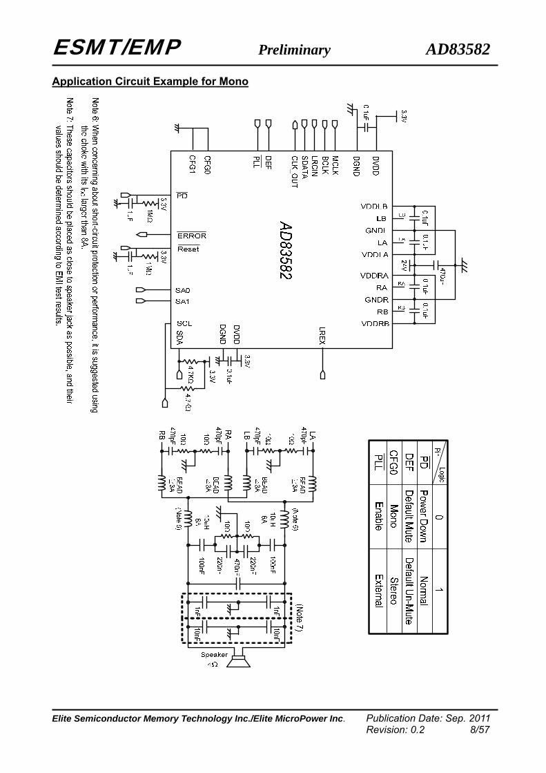
Application Circuit Example for Mono

ESMT/EMP Preliminary AD83582
Elite Semiconductor Memory Technology Inc./Elite MicroPower Inc. Publication Date: Sep. 2011 Revision: 0.2 9/57
Application Circuit Example for Single Chip 2.1CH (SEx2 + BTLx1)
ESMT/EMP Preliminary AD83582
Elite Semiconductor Memory Technology Inc./Elite MicroPower Inc. Publication Date: Sep. 2011 Revision: 0.2 10/57
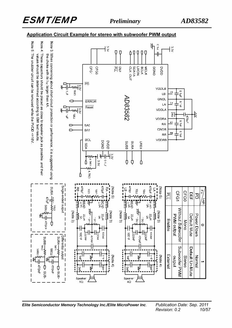
Application Circuit Example for stereo with subwoofer PWM output

ESMT/EMP Preliminary AD83582
Elite Semiconductor Memory Technology Inc./Elite MicroPower Inc. Publication Date: Sep. 2011 Revision: 0.2 11/57
Electrical Characteristics and Specifications for Loudspeaker BTL output for stereo Condition: DVDD =3.3V, VDDL=VDDR=24V, FS=48kHz, Load=8 with passive LC lowpass filter (L=22μH
with RDC=0.12Ω, C=470nF); Input is 1kHz sinewave. Volume is 0dB unless otherwise specified.
Symbol Parameter Condition Input Level Min Typ Max Units
RMS Output Power (THD+N=10%) +8dB volume -6dB 35 WPO
(Note 9) RMS Output Power (THD+N=1%) +8dB volume -7.8dB 28 W
THD+N Total Harmonic Distortion + Noise Po=21.8W -1dB 0.37 %
SNR Signal to Noise Ratio(Note 8) Po=21.8W -1dB 98 dB
DR Dynamic Range(Note 8) -60dB 108 dB
PSRR Power Supply Rejection Ratio -60dB 60 dB
Channel Separation 1W @1kHz -1dB 60 dB
Efficiency 85 η Efficiency at Power Saving Mode
THD+N=10% -6dB 88.5
%
Note 8: Measured with A-weighting filter.
Note 9: Thermal dissipation is limited by package type and PCB design. The external heat-sink or system
cooling method should be adopted for maximum power output.
Total Harmonic Distortion + Noise vs. Output Power (Stereo)
ESMT/EMP Preliminary AD83582
Elite Semiconductor Memory Technology Inc./Elite MicroPower Inc. Publication Date: Sep. 2011 Revision: 0.2 12/57
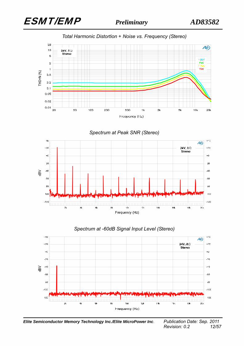
Total Harmonic Distortion + Noise vs. Frequency (Stereo)
Spectrum at Peak SNR (Stereo)
Spectrum at -60dB Signal Input Level (Stereo)

ESMT/EMP Preliminary AD83582
Elite Semiconductor Memory Technology Inc./Elite MicroPower Inc. Publication Date: Sep. 2011 Revision: 0.2 13/57
Efficiency (Stereo)
Efficiency vs. Output Power (Stereo)
0
10
20
30
40
50
60
70
80
90
100
0 10 20 30 40 50 60 702CH Output Power(W)
Effic
ienc
y(%
)
12V15V18V24V
Efficiency (Stereo) for Power Saving Mode
Efficiency vs. Output Power (Stereo)
0
10
20
30
40
50
60
70
80
90
100
0 10 20 30 40 50 60 702CH Output Power(W)
Effic
ienc
y(%
)
24V Power Saving Mode24V

ESMT/EMP Preliminary AD83582
Elite Semiconductor Memory Technology Inc./Elite MicroPower Inc. Publication Date: Sep. 2011 Revision: 0.2 14/57
Electrical Characteristics and Specifications for Loudspeaker (cont.) BTL output for mono Condition: DVDD= 3.3V, VDDL=VDDR=24V, FS=48kHz, Load=4 with passive LC lowpass filter (L=10μH
with RDC=0.12Ω, C=470nF); Input is 1kHz sinewave. Volume is 0dB unless otherwise specified.
Symbol Parameter Condition Input Level Min Typ Max Units
RMS Output Power (THD+N=10%) +8dB volume -5.8dB 69 WPO
(Note 9) RMS Output Power (THD+N=1%) +8dB volume -7.8dB 56 W
THD+N Total Harmonic Distortion + Noise Po=44W -1dB 0.4 %
SNR Signal to Noise Ratio(Note 8) Po=44W -1dB 97 dB
DR Dynamic Range(Note 8) -60dB 106 dB
PSRR Power Supply Rejection Ratio -60dB 60 dB
Efficiency 86 η Efficiency at Power Saving Mode
THD+N=10% 0dB 86.5
%
Note 8: Measured with A-weighting filter.
Note 9: Thermal dissipation is limited by package type and PCB design. The external heat-sink or system
cooling method should be adopted for maximum power output.
Total Harmonic Distortion + Noise vs. Output Power (Mono)

ESMT/EMP Preliminary AD83582
Elite Semiconductor Memory Technology Inc./Elite MicroPower Inc. Publication Date: Sep. 2011 Revision: 0.2 15/57
Total Harmonic Distortion + Noise vs. Frequency (Mono)
Spectrum at Peak SNR (Mono)
Spectrum at -60dB Signal Input Level (Mono)

ESMT/EMP Preliminary AD83582
Elite Semiconductor Memory Technology Inc./Elite MicroPower Inc. Publication Date: Sep. 2011 Revision: 0.2 16/57
Efficiency (Mono)
Efficiency vs. Output Power (Mono)
0
10
20
30
40
50
60
70
80
90
100
0 10 20 30 40 50 60 70
Output Power(W)
Effi
cien
cy(%
)
12V15V18V24V
4Mono
Efficiency (Mono) for Power Saving Mode
Efficiency vs. Output Power (Mono)
0
10
20
30
40
50
60
70
80
90
100
0 10 20 30 40 50 60
Output Power(W)
Effi
cien
cy(%
)
24V Power Saving Mode24V
ESMT/EMP Preliminary AD83582
Elite Semiconductor Memory Technology Inc./Elite MicroPower Inc. Publication Date: Sep. 2011 Revision: 0.2 17/57
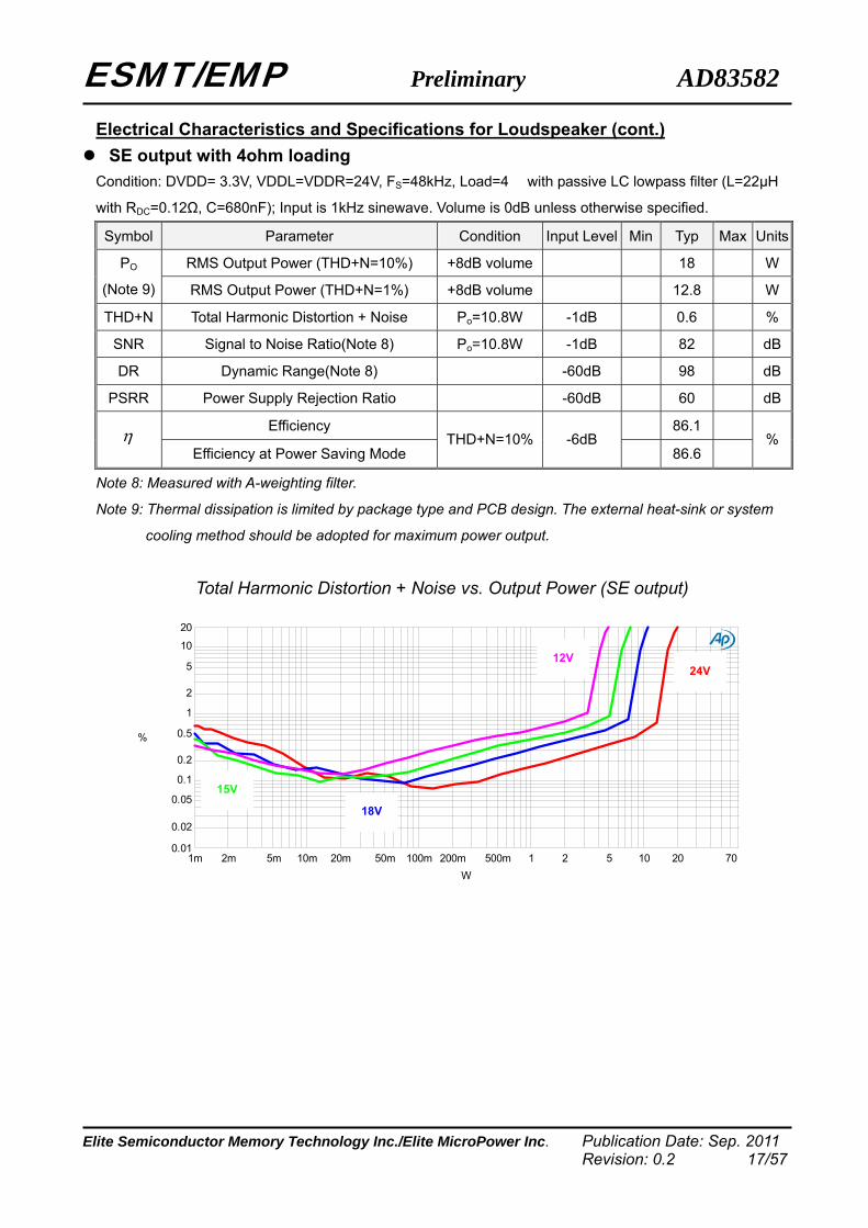
Electrical Characteristics and Specifications for Loudspeaker (cont.) SE output with 4ohm loading Condition: DVDD= 3.3V, VDDL=VDDR=24V, FS=48kHz, Load=4 with passive LC lowpass filter (L=22μH
with RDC=0.12Ω, C=680nF); Input is 1kHz sinewave. Volume is 0dB unless otherwise specified.
Symbol Parameter Condition Input Level Min Typ Max Units
RMS Output Power (THD+N=10%) +8dB volume 18 WPO
(Note 9) RMS Output Power (THD+N=1%) +8dB volume 12.8 W
THD+N Total Harmonic Distortion + Noise Po=10.8W -1dB 0.6 %
SNR Signal to Noise Ratio(Note 8) Po=10.8W -1dB 82 dB
DR Dynamic Range(Note 8) -60dB 98 dB
PSRR Power Supply Rejection Ratio -60dB 60 dB
Efficiency 86.1 η Efficiency at Power Saving Mode
THD+N=10% -6dB 86.6
%
Note 8: Measured with A-weighting filter.
Note 9: Thermal dissipation is limited by package type and PCB design. The external heat-sink or system
cooling method should be adopted for maximum power output.
Total Harmonic Distortion + Noise vs. Output Power (SE output)
0.01
20
0.02
0.05
0.1
0.2
0.5
1
2
5
10
%
1m 702m 5m 10m 20m 50m 100m 200m 500m 1 2 5 10 20W
24V
18V
15V
12V

ESMT/EMP Preliminary AD83582
Elite Semiconductor Memory Technology Inc./Elite MicroPower Inc. Publication Date: Sep. 2011 Revision: 0.2 18/57
Total Harmonic Distortion + Noise vs. Frequency (SE output)
0.01
20
0.02
0.05
0.1
0.2
0.5
1
2
5
10
%
20 20k50 100 200 500 1k 2k 5k 10kHz
5W
2.5W
1W
0.5W
24V, 4Ohm2.1CH
0.01
20
0.02
0.05
0.1
0.2
0.5
1
2
5
10
%
20 20k50 100 200 500 1k 2k 5k 10kHz
5W
2.5W
1W
0.5W
24V, 4Ohm2.1CH
Spectrum at Peak SNR (SE output)
-120
+40
-100
-80
-60
-40
-20
+0
+20
dBV
2k 20k4k 6k 8k 10k 12k 14k 16k 18kHz
Spectrum at -60dB Signal Input Level (SE output)
-120
+40
-100
-80
-60
-40
-20
+0
+20
dBV
2k 20k4k 6k 8k 10k 12k 14k 16k 18kHz
ESMT/EMP Preliminary AD83582
Elite Semiconductor Memory Technology Inc./Elite MicroPower Inc. Publication Date: Sep. 2011 Revision: 0.2 19/57
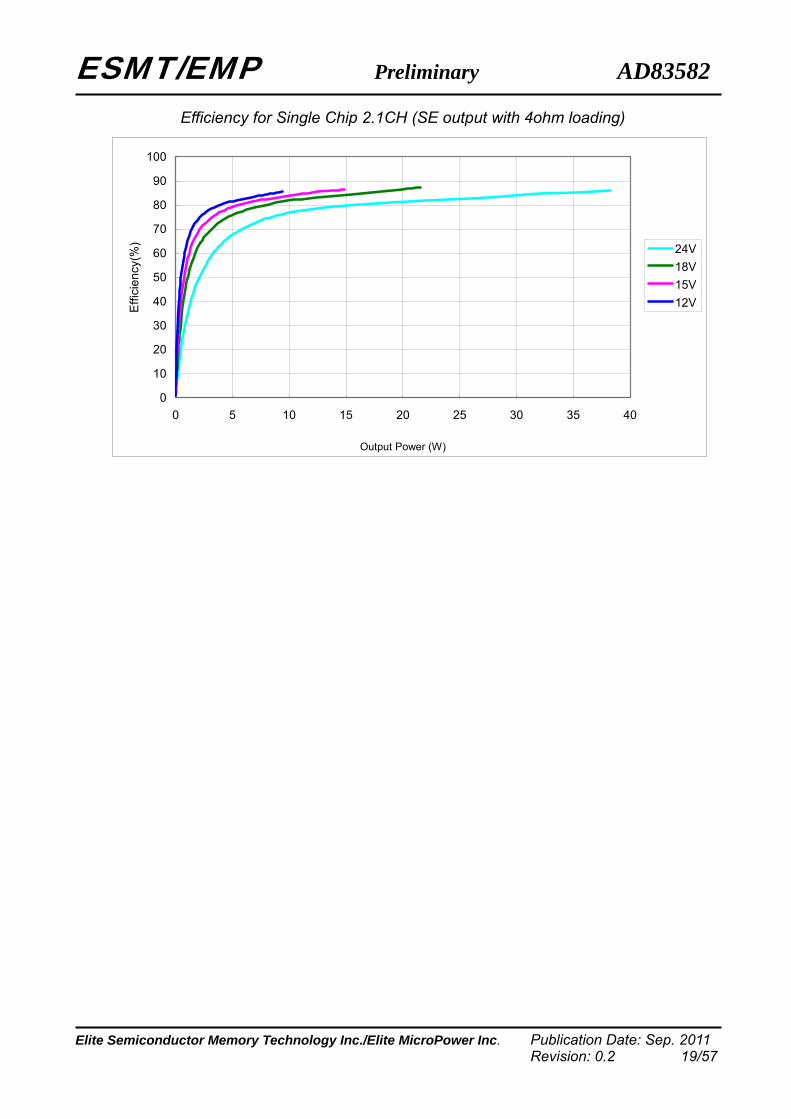
Efficiency for Single Chip 2.1CH (SE output with 4ohm loading)
0
10
20
30
40
50
60
70
80
90
100
0 5 10 15 20 25 30 35 40
Output Power (W)
Effi
cien
cy(%
) 24V18V15V12V

ESMT/EMP Preliminary AD83582
Elite Semiconductor Memory Technology Inc./Elite MicroPower Inc. Publication Date: Sep. 2011 Revision: 0.2 20/57
Electrical Characteristics and Specifications for Loudspeaker (cont.) SE output with 8ohm loading Condition: DVDD= 3.3V, VDDL=VDDR=24V, FS=48kHz, Load=8 with passive LC lowpass filter (L=22μH
with RDC=0.12Ω, C=680nF); Input is 1kHz sinewave. Volume is 0dB unless otherwise specified.
Symbol Parameter Condition Input Level Min Typ Max Units
RMS Output Power (THD+N=10%) +8dB volume 10 WPO
(Note 9) RMS Output Power (THD+N=1%) +8dB volume 8 W
THD+N Total Harmonic Distortion + Noise Po=6.1W -1dB 0.3 %
SNR Signal to Noise Ratio(Note 8) Po=6.1W -1dB 85 dB
DR Dynamic Range(Note 8) -60dB 98 dB
PSRR Power Supply Rejection Ratio -60dB 60 dB
Efficiency 89 η Efficiency at Power Saving Mode
THD+N=10% -6dB 89.9
%
Note 8: Measured with A-weighting filter.
Note 9: Thermal dissipation is limited by package type and PCB design. The external heat-sink or system
cooling method should be adopted for maximum power output.
Total Harmonic Distortion + Noise vs. Output Power (SE output)
0.01
20
0.02
0.05
0.1
0.2
0.5
1
2
5
10
%
1m 602m 5m 10m 20m 50m 100m 200m 500m 1 2 5 10 20W
24V
18V
15V
12V

ESMT/EMP Preliminary AD83582
Elite Semiconductor Memory Technology Inc./Elite MicroPower Inc. Publication Date: Sep. 2011 Revision: 0.2 21/57
Total Harmonic Distortion + Noise vs. Frequency (SE output)
0.01
20
0.02
0.05
0.1
0.2
0.5
1
2
5
10
%
20 20k50 100 200 500 1k 2k 5k 10kHz
Spectrum at Peak SNR (SE output)
-120
+40
-100
-80
-60
-40
-20
+0
+20
dBV
2k 20k4k 6k 8k 10k 12k 14k 16k 18kHz
Spectrum at -60dB Signal Input Level (SE output)
-120
+40
-100
-80
-60
-40
-20
+0
+20
dBV
2k 20k4k 6k 8k 10k 12k 14k 16k 18kHz
2W
1W
0.5W 0.25W
ESMT/EMP Preliminary AD83582
Elite Semiconductor Memory Technology Inc./Elite MicroPower Inc. Publication Date: Sep. 2011 Revision: 0.2 22/57
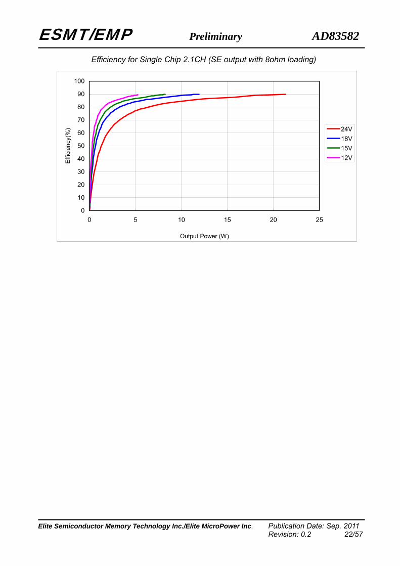
Efficiency for Single Chip 2.1CH (SE output with 8ohm loading)
0
10
20
30
40
50
60
70
80
90
100
0 5 10 15 20 25
Output Power (W)
Effi
cien
cy(%
) 24V18V15V12V
ESMT/EMP Preliminary AD83582
Elite Semiconductor Memory Technology Inc./Elite MicroPower Inc. Publication Date: Sep. 2011 Revision: 0.2 23/57
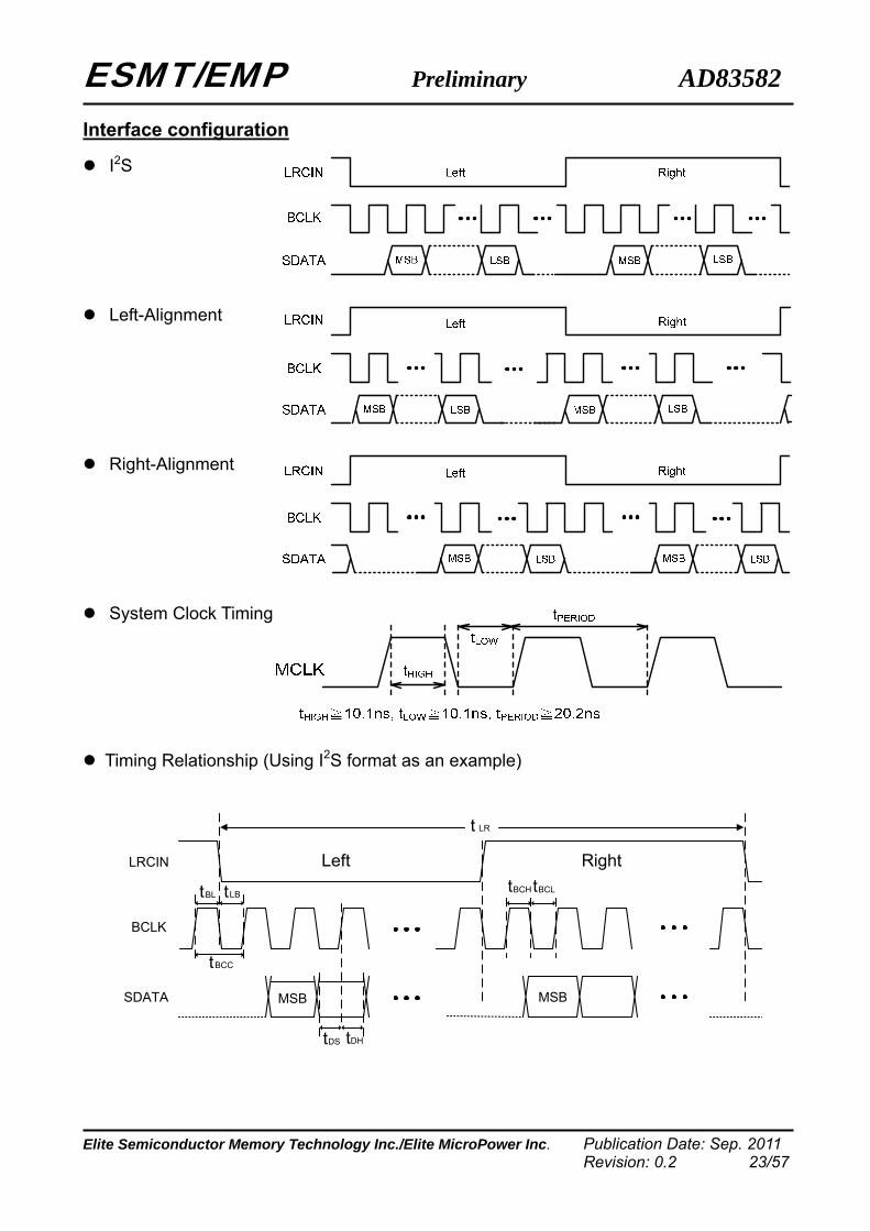
Interface configuration
I2S
Left-Alignment
Right-Alignment
System Clock Timing
Timing Relationship (Using I2S format as an example)
LRCIN
BCLK
SDATA
Left Right
MSB MSB
t LR
tBL tLB
tBCC
tDS tDH
tBCHtBCL
ESMT/EMP Preliminary AD83582
Elite Semiconductor Memory Technology Inc./Elite MicroPower Inc. Publication Date: Sep. 2011 Revision: 0.2 24/57
Symbol Parameter Min Typ Max Units
tLR LRCIN Period (1/FS) 10.41 31.25 s
tBL BCLK Rising Edge to LRCIN Edge 50 ns
tLB LRCIN Edge to BCLK Rising Edge 50 ns
tBCC BCLK Period (1/64FS) 162.76 488.3 ns
tBCH BCLK Pulse Width High 81.38 244 ns
tBCL BCLK Pulse Width Low 81.38 244 ns
tDS SDATA Set-Up Time 50 ns
tDH SDATA Hold Time 50 ns
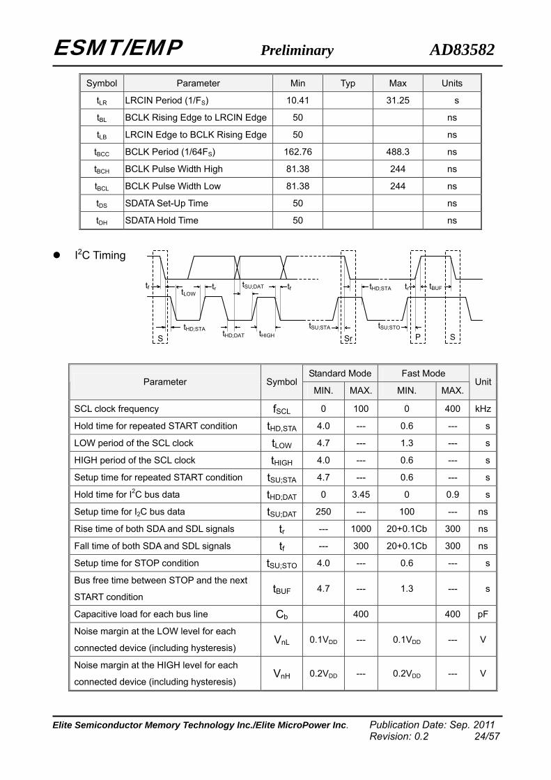
I2C Timing
tf
tHD;STA
tLOWtr
tHD;DAT
tSU;DAT tf
tHIGH
tSU;STA
tHD;STA
tSU;STO
tr tBUF
S Sr P S
Standard Mode Fast Mode
Parameter SymbolMIN. MAX. MIN. MAX.
Unit
SCL clock frequency fSCL 0 100 0 400 kHz
Hold time for repeated START condition tHD,STA 4.0 --- 0.6 --- s
LOW period of the SCL clock tLOW 4.7 --- 1.3 --- s
HIGH period of the SCL clock tHIGH 4.0 --- 0.6 --- s
Setup time for repeated START condition tSU;STA 4.7 --- 0.6 --- s
Hold time for I2C bus data tHD;DAT 0 3.45 0 0.9 s
Setup time for I2C bus data tSU;DAT 250 --- 100 --- ns
Rise time of both SDA and SDL signals tr --- 1000 20+0.1Cb 300 ns
Fall time of both SDA and SDL signals tf --- 300 20+0.1Cb 300 ns
Setup time for STOP condition tSU;STO 4.0 --- 0.6 --- s
Bus free time between STOP and the next
START condition tBUF 4.7 --- 1.3 --- s
Capacitive load for each bus line Cb 400 400 pF
Noise margin at the LOW level for each
connected device (including hysteresis) VnL 0.1VDD --- 0.1VDD --- V
Noise margin at the HIGH level for each
connected device (including hysteresis) VnH 0.2VDD --- 0.2VDD --- V
ESMT/EMP Preliminary AD83582
Elite Semiconductor Memory Technology Inc./Elite MicroPower Inc. Publication Date: Sep. 2011 Revision: 0.2 25/57
Operation Description Operation modes
(i) Without I2C control
The default settings, Bass, Treble, EQ, Volume, DRC, PLL, Subwoofer Bandwidth, …, and Sub-woofer
gain are applied to register table content when using AD83582 without I2C control. The more information
about default settings, please refer to the highlighted column of register table section.
(ii) With I2C control
When using I2C control, user can program suitable parameters into AD83582 for their specific applications.
Please refer to the register table section to get the more detail.
Reset
When the RESET pin is lowered, AD83582 will clear the stored data and reset the register table to default
values. AD83582 will exit reset state at the 256th MCLK cycle after the RESET pin is raised to high.
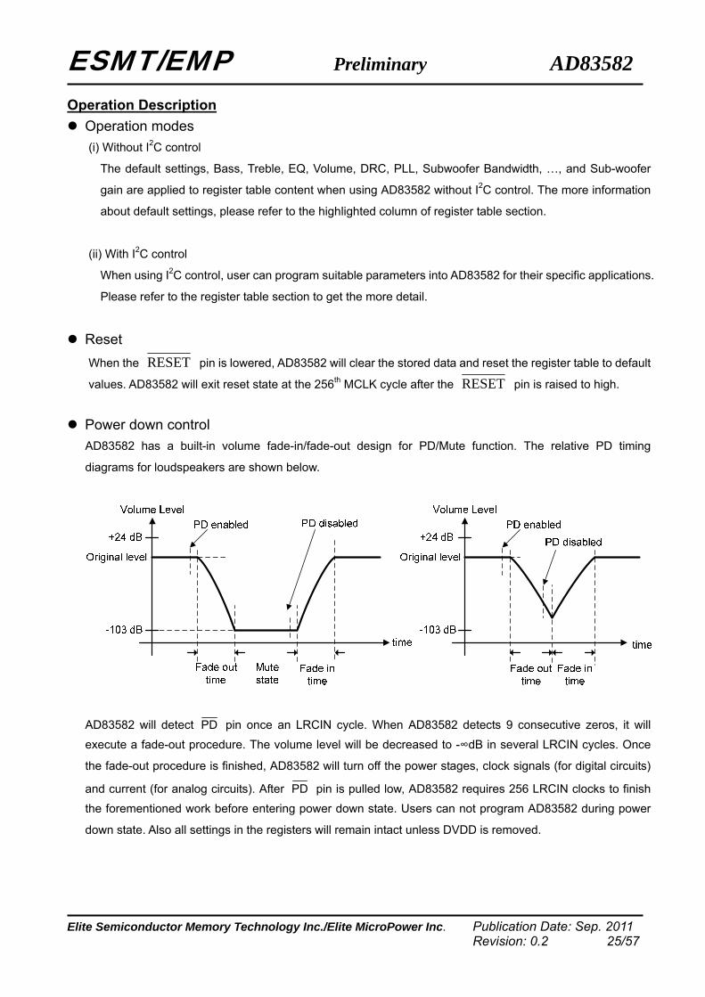
Power down control
AD83582 has a built-in volume fade-in/fade-out design for PD/Mute function. The relative PD timing
diagrams for loudspeakers are shown below.
AD83582 will detect PD pin once an LRCIN cycle. When AD83582 detects 9 consecutive zeros, it will execute a fade-out procedure. The volume level will be decreased to -∞dB in several LRCIN cycles. Once
the fade-out procedure is finished, AD83582 will turn off the power stages, clock signals (for digital circuits)
and current (for analog circuits). After PD pin is pulled low, AD83582 requires 256 LRCIN clocks to finish the forementioned work before entering power down state. Users can not program AD83582 during power
down state. Also all settings in the registers will remain intact unless DVDD is removed.
ESMT/EMP Preliminary AD83582
Elite Semiconductor Memory Technology Inc./Elite MicroPower Inc. Publication Date: Sep. 2011 Revision: 0.2 26/57
When AD83582 detect 9 consecutive ones from PD pin, the PD function will be disabled and a fade-in procedure is then executed. If the PD signal is removed during the fade-out procedure (above, right figure),
AD83582 will still execute the fade-in procedure. In addition, AD83582 will establish the analog circuits’ bias
current and send the clock signals to digital circuits. Afterwards, AD83582 will return to its normal status.
Internal PLL (PLL )
AD83582 has a built-in PLL internally. When the external MCLK clock is high quality enough, you can bypass
the PLL function by pulling the PLL pin is high. Otherwise, the internal PLL with an external reference MCLK
is highly recommended.
Self-protection circuits
AD83582 has built-in protection circuits including thermal, short-circuit and under-voltage detection circuits.
(i) When the internal junction temperature is higher than 160 , power stages will be turned off and
AD83582 will return to normal operation once the temperature drops to 120 . The temperature values
may vary around 10%.
(ii) The short-circuit protection circuit protects the output stage when the wires which are connected to
loudspeakers are shorted to each other or GND/VDD. For normal 24V operations, the current flowing
through the power stage will be less than 5Afor stereo configuration or less than 10A for mono
configuration. Otherwise, the short-circuit detectors may pull the ERROR pin to DGND, disabling the
output stages. When the over-temperature or short-circuit condition occurs, the open-drain ERROR
pin will be pulled low and latched into ERROR state.
Once the over-temperature or short-circuit condition is removed, AD83582 will exit ERROR state when
one of the following conditions is met: (1) RESET pin is pulled low, (2)PD pin is pulled low, (3) Master mute is enabled through the I2C interface.
(iii) Once the DVDD voltage is lower than 2.7V, AD83582 will turn off its loudspeaker power stages and
cease the operation of digital processing circuits. When DVDD becomes larger than 2.8V, AD83582 will
return to normal operation.

ESMT/EMP Preliminary AD83582
Elite Semiconductor Memory Technology Inc./Elite MicroPower Inc. Publication Date: Sep. 2011 Revision: 0.2 27/57
Anti-pop design AD83582 will generate appropriate control signals to suppress pop sounds during initial power on/off, power
down/up, mute, and volume level changes.
Power on sequence Hereunder is AD82581’s power on sequence. Please note that we suggested users set DEF pin at low state
initially, and than give a de-mute command via I2C when the whole system is stable.
PVDD
DVDD
MCLK
RESET
SCL
SDA
de-mute
Note. Set DEF pin at low state initially
3D surround sound AD83582 provides the virtual surround sound technology with greater separation and depth voice quality for
stereo signals.

ESMT/EMP Preliminary AD83582
Elite Semiconductor Memory Technology Inc./Elite MicroPower Inc. Publication Date: Sep. 2011 Revision: 0.2 28/57
Output configuration CFG0 and CFG1 define the configuration mode. AD83582 can be configured to stereo, mono, 2.1CH and
stereo with subwoofer output mode. Table1 provides a reference of available configuration.
Table 1.
CFG1 CFG0 Configuration Mode
0 0 Mono
0 1 Stereo
1 0 2.1CH
1 1 Stereo with subwoofer output
Configuration figures:

ESMT/EMP Preliminary AD83582
Elite Semiconductor Memory Technology Inc./Elite MicroPower Inc. Publication Date: Sep. 2011 Revision: 0.2 29/57
I2C-Bus Transfer Protocol
Introduction AD83582 employs I2C-bus transfer protocol. Two wires, serial data and serial clock carry information
between the devices connected to the bus. Each device is recognized by a unique 7-bit address and can
operate as either a transmitter or a receiver. The master device initiates a data transfer and provides the
serial clock on the bus. AD83582 is always an I2C slave device.
Protocol
START and STOP condition START is identified by a high to low transition of the SDA signal.. A START condition must precede
any command for data transfer. A STOP is identified by a low to high transition of the SDA signal. A
STOP condition terminates communication between AD83582 and the master device on the bus. In
both START and STOP, the SCL is stable in the high state.
Data validity The SDA signal must be stable during the high period of the clock. The high or low change of SDA only
occurs when SCL signal is low. AD83582 samples the SDA signal at the rising edge of SCL signal.
Device addressing The master generates 7-bit address to recognize slave devices. When AD83582 receives 7-bit
address matched with 0110x0y (where x and y can be selected by external SA0 and SA1 pins,
respectively), AD83582 will acknowledge at the 9th bit (the 8th bit is for R/W bit). The bytes following
the device identification address are for AD83582 internal sub-addresses.
Data transferring Each byte of SDA signaling must consist of 8 consecutive bits, and the byte is followed by an
acknowledge bit. Data is transferred with MSB first, as shown in the figure below. In both write and
read operations, AD83582 supports both single-byte and multi-byte transfers. Refer to the figure
below for detailed data-transferring protocol.

ESMT/EMP Preliminary AD83582
Elite Semiconductor Memory Technology Inc./Elite MicroPower Inc. Publication Date: Sep. 2011 Revision: 0.2 30/57
Register Table
The AD83582’s audio signal processing data flow is shown below. Users can control these functions by
programming appropriate settings in the register table. In this section, the register table is summarized first. The
definition of each register follows in the next section.
Address Name B[7] B[6] B[5] B[4] B[3] B[2] B[1] B[0]
0X00 SCTL1 IF[2] IF[1] IF[0] Reserved LREXC
0X01 SCTL2 Reserved FS[1] FS[0] PMF[3] PMF[2] PMF[1] PMF[0]
0X02 SCTL3 EN_CLKO Reserved MMUTE CM1 CM2 CM3
0X03 MVOL MV[7] MV[6] MV[5] MV[4] MV[3] MV[2] MV[1] MV[0]
0X04 C1VOL C1V[7] C1V[6] C1V[5] C1V[4] C1V[3] C1V[2] C1V[1] C1V[0]
0X05 C2VOL C2V[7] C2V[6] C2V[5] C2V[4] C2V[3] C2V[2] C2V[1] C2V[0]
0X06 C3VOL C3V[7] C3V[6] C3V[5] C3V[4] C3V[3] C3V[2] C3V[1] C3V[0]
0X07 BTONE Reserved BTC[4] BTC[3] BTC[2] BTC[1] BTC[0]
0X08 TTONE Reserved TTC[4] TTC[3] TTC[2] TTC[1] TTC[0]
0X09 AUTO1 Reserved XO[3] XO[2] XO[1] XO[0]
0X0A SCTL4 SRBP BTE Reserved ZDE EQL PSL DSPB HPB
0X0B C1CFG Reserved C1DRCBP C1HPFBP C1VBP
0X0C C2CFG Reserved C2DRCBP C2HPFBP C2VBP
0X0D C3CFG Reserved C3DRCBP C3HPFBP C3VBP

ESMT/EMP Preliminary AD83582
Elite Semiconductor Memory Technology Inc./Elite MicroPower Inc. Publication Date: Sep. 2011 Revision: 0.2 31/57
0X0E LAR LA[3] LA[2] LA[1] LA[0] LR[3] LR[2] LR[1] LR[0]
0X0F LATRT LAT[3] LAT[2] LAT[1] LAT[0] LRT[3] LRT[2] LRT[1] LRT[0]
0X10 ERDLY Reserved
0X11 SCTL5 Reserved SW_RSTB Reserved DIS_MCLK_DET QT_EN PWM_SEL
0X12 HVUV Reserved HV_UVSEL [3] HV_UVSEL [2] HV_UVSEL [1] HV_UVSEL [0]
0X13 ZDCFG Reserved ZD_LEVEL[1] ZD_LEVEL[0] ZD_GAIN[1] ZD_GAIN[0]
0X14 CFADDR Reserved CFA[6] CFA[5] CFA[4] CFA[3] CFA[2] CFA[1] CFA[0]
0X15 A1CF1 C1B[23] C1B[22] C1B[21] C1B[20] C1B[19] C1B[18] C1B[17] C1B[16]
0X16 A1CF2 C1B[15] C1B[14] C1B[13] C1B[12] C1B[11] C1B[10] C1B[9] C1B[8]
0X17 A1CF3 C1B[7] C1B[6] C1B[5] C1B[4] C1B[3] C1B[2] C1B[1] C1B[0]
0X18 A2CF1 C2B[23] C2B[22] C2B[21] C2B[20] C2B[19] C2B[18] C2B[17] C2B[16]
0X19 A2CF2 C2B[15] C2B[14] C2B[13] C2B[12] C2B[11] C2B[10] C2B[9] C2B[8]
0X1A A2CF3 C2B[7] C2B[6] C2B[5] C2B[4] C2B[3] C2B[2] C2B[1] C2B[0]
0X1B B1CF1 C3B[23] C3B[22] C3B[21] C3B[20] C3B[19] C3B[18] C3B[17] C3B[16]
0X1C B1CF2 C3B[15] C3B[14] C3B[13] C3B[12] C3B[11] C3B[10] C3B[9] C3B[8]
0X1D B1CF3 C3B[7] C3B[6] C3B[5] C3B[4] C3B[3] C3B[2] C3B[1] C3B[0]
0X1E B2CF1 C4B[23] C4B[22] C4B[21] C4B[20] C4B[19] C4B[18] C4B[17] C4B[16]
0X1F B2CF2 C4B[15] C4B[14] C4B[13] C4B[12] C4B[11] C4B[10] C4B[9] C4B[8]
0X20 B2CF3 C4B[7] C4B[6] C4B[5] C4B[4] C4B[3] C4B[2] C4B[1] C4B[0]
0X21 A0CF1 C5B[23] C5B[22] C5B[21] C5B[20] C5B[19] C5B[18] C5B[17] C5B[16]
0X22 A0CF2 C5B[15] C5B[14] C5B[13] C5B[12] C5B[11] C5B[10] C5B[9] C5B[8]
0X23 A0CF3 C5B[7] C5B[6] C5B[5] C5B[4] C5B[3] C5B[2] C5B[1] C5B[0]
0X24 CFUD Reserved RA R1 WA W1
0X25 FDCFG Reserved
0X26 MBIST Reserved
0X27 Status Reserved
0X28 PWM_CT
RL Reserved
0X29 TM_CTR
L Reserved
0X2A QT_SW_LE
VEL Reserved
QT_SW_LEVEL
[4]
QT_SW_LEVEL
[3]
QT_SW_LEVEL
[2]
QT_SW_LEVEL
[1]
QT_SW_LEVEL
[0]

ESMT/EMP Preliminary AD83582
Elite Semiconductor Memory Technology Inc./Elite MicroPower Inc. Publication Date: Sep. 2011 Revision: 0.2 32/57
Detail Description for Register Note that the highlighted columns are default values of these tables. If there is no highlighted value, the default
setting of this bit is determined by the external pin.
Address 0 : State control 1 AD83582 supports multiple serial data input formats including I2S, Left-alignment and Right-alignment.
These formats is selected by users via bit7~bit5 of address 0. The left/right channels can be exchanged to
each other by programming to address 0/bit0, LREXC.
BIT NAME DESCRIPTION VALUE FUNCTION
000 I2S 16-24 bits
001 Left-alignment 16-24 bits
010 Right-alignment 16 bits
011 Right-alignment 18 bits
100 Right-alignment 20 bits
B[7:5] IF[2:0] Input Format
101 Right-alignment 24 bits
B[4] Reserved
B[3] Reserved
B[2] Reserved
B[1] Reserved
0 No exchanged B[0] LREXC
Left/Right (L/R)
Channel exchanged 1 L/R exchanged
Address 1 : State control 2 AD83582 has a built-in PLL which can be bypassed by pulling the PLL pin High. When PLL is bypassed,
AD83582 only supports 1024x, 512x and 256x MCLK/Fs ratio for Fs is 32/44.1/48kHz, 64/88.2/96kHz, and
128/176.4/192kHz respectively. When PLL is enabled, multiple MCLK/Fs ratios are supported. Detail setting
is shown in the following table.
BIT NAME DESCRIPTION VALUE FUNCTION
B[7:6] Reserved
00 32/44.1/48kHz
01 64/88.2/96kHz B[5:4] FS[1:0] Sampling Frequency
1x 128/176.4/192kHz
ESMT/EMP Preliminary AD83582
Elite Semiconductor Memory Technology Inc./Elite MicroPower Inc. Publication Date: Sep. 2011 Revision: 0.2 33/57
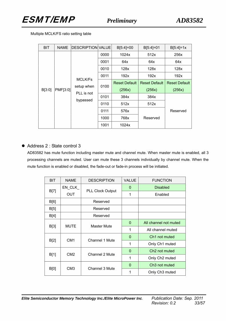
Multiple MCLK/FS ratio setting table
BIT NAME DESCRIPTION VALUE B[5:4]=00 B[5:4]=01 B[5:4]=1x
0000 1024x 512x 256x
0001 64x 64x 64x
0010 128x 128x 128x
0011 192x 192x 192x
0100Reset Default
(256x)
Reset Default
(256x)
Reset Default
(256x)
0101 384x 384x
0110 512x 512x
0111 576x
1000 768x
B[3:0] PMF[3:0]
MCLK/Fs
setup when
PLL is not
bypassed
1001 1024x
Reserved
Reserved
Address 2 : State control 3 AD83582 has mute function including master mute and channel mute. When master mute is enabled, all 3
processing channels are muted. User can mute these 3 channels individually by channel mute. When the
mute function is enabled or disabled, the fade-out or fade-in process will be initiated.
BIT NAME DESCRIPTION VALUE FUNCTION
0 Disabled B[7]
EN_CLK_
OUT PLL Clock Output
1 Enabled
B[6] Reserved
B[5] Reserved
B[4] Reserved
0 All channel not muted B[3] MUTE Master Mute
1 All channel muted
0 Ch1 not muted B[2] CM1 Channel 1 Mute
1 Only Ch1 muted
0 Ch2 not muted B[1] CM2 Channel 2 Mute
1 Only Ch2 muted
0 Ch3 not muted B[0] CM3 Channel 3 Mute
1 Only Ch3 muted

ESMT/EMP Preliminary AD83582
Elite Semiconductor Memory Technology Inc./Elite MicroPower Inc. Publication Date: Sep. 2011 Revision: 0.2 34/57
Address 3 : Master volume control AD83582 supports both master-volume (Address 3) and channel-volume control (Address 4, 5 and 6) modes.
Both volume control settings range from +12dB ~ -103dB and 0.5dB per step. Note that the master volume
control is added to the individual channel volume control as the total volume control. For example, if the
master volume level is set at, Level A (in dB unit) and the channel volume level is set at Level B (in dB unit),
the total volume control setting is equal to Level A plus with Level B.
-103dB Total ≦ volume ( Level A + Level B ) +24dB.≦
BIT NAME DESCRIPTION VALUE FUNCTION
00000000 +12.0dB
00000001 +11.5dB
00000010 +11.0dB
︰ ︰
00010111 +0.5dB
00011000 0.0dB
00011001 -0.5dB
︰ ︰
11100110 -103.0dB
11100111 -∞dB
︰ ︰
BIT[7:0] MV[7:0] Master Volume
11111111 -∞dB
Address 4 : Channel 1 volume
BIT NAME DESCRIPTION VALUE FUNCTION
00000000 +12.0dB
00000001 +11.5dB
00000010 +11.0dB
︰ ︰
00010111 +0.5dB
00011000 0.0dB
00011001 -0.5dB
︰ ︰
11100110 -103.0dB
11100111 -∞dB
︰ ︰
BIT[7:0] C1V[7:0] Channel1 Volume
11111111 -∞dB

ESMT/EMP Preliminary AD83582
Elite Semiconductor Memory Technology Inc./Elite MicroPower Inc. Publication Date: Sep. 2011 Revision: 0.2 35/57
Address 5 : Channel 2 volume
BIT NAME DESCRIPTION VALUE FUNCTION
00000000 +12.0dB
00000001 +11.5dB
00000010 +11.0dB
︰ ︰
00010111 +0.5dB
00011000 0.0dB
00011001 -0.5dB
︰ ︰
11100110 -103.0dB
11100111 -∞dB
︰ ︰
BIT[7:0] C2V[7:0] Channel2 Volume
11111111 -∞dB
Address 6 : Channel 3 volume
BIT NAME DESCRIPTION VALUE FUNCTION
00000000 +12.0dB
00000001 +11.5dB
00000010 +11.0dB
︰ ︰
00010111 +0.5dB
00011000 0.0dB
00011001 -0.5dB
︰ ︰
11100110 -103.0dB
11100111 -∞dB
︰ ︰
BIT[7:0] C3V[7:0] Channel3 Volume
11111111 -∞dB
ESMT/EMP Preliminary AD83582
Elite Semiconductor Memory Technology Inc./Elite MicroPower Inc. Publication Date: Sep. 2011 Revision: 0.2 36/57
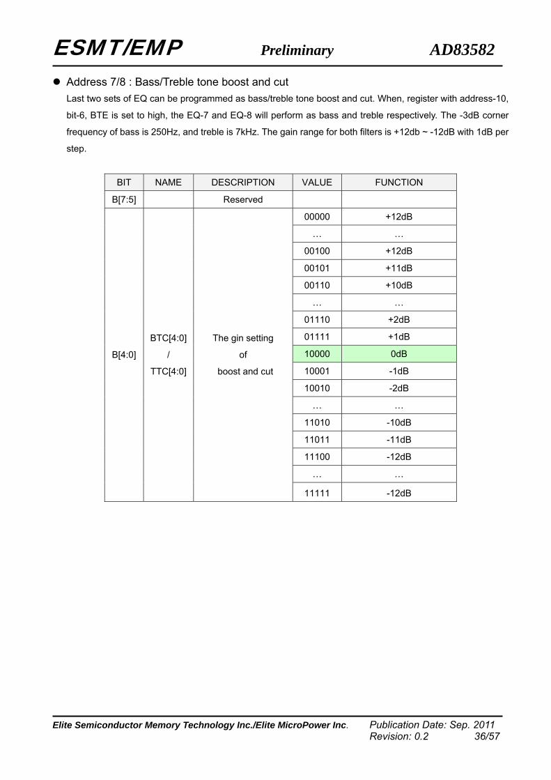
Address 7/8 : Bass/Treble tone boost and cut Last two sets of EQ can be programmed as bass/treble tone boost and cut. When, register with address-10,
bit-6, BTE is set to high, the EQ-7 and EQ-8 will perform as bass and treble respectively. The -3dB corner
frequency of bass is 250Hz, and treble is 7kHz. The gain range for both filters is +12db ~ -12dB with 1dB per
step.
BIT NAME DESCRIPTION VALUE FUNCTION
B[7:5] Reserved
00000 +12dB
… …
00100 +12dB
00101 +11dB
00110 +10dB
… …
01110 +2dB
01111 +1dB
10000 0dB
10001 -1dB
10010 -2dB
… …
11010 -10dB
11011 -11dB
11100 -12dB
… …
B[4:0]
BTC[4:0]
/
TTC[4:0]
The gin setting
of
boost and cut
11111 -12dB

ESMT/EMP Preliminary AD83582
Elite Semiconductor Memory Technology Inc./Elite MicroPower Inc. Publication Date: Sep. 2011 Revision: 0.2 37/57
Address 9 : Bass management crossover frequency The AD83582 provides bass management crossover frequency selection. A 1st order high-pass filter
(channel 1 and 2) and a 2nd order low-pass filter (channel 3) at selected frequency are performed.
BIT NAME DESCRIPTION VALUE FUNCTION
B[7:4] Reserved
0000 80Hz
0001 100Hz
0010 120Hz
0011 140Hz
0100 160Hz
0101 180Hz
0110 200Hz
0111 220Hz
1000 240Hz
1001 260Hz
1010 280Hz
1011 300Hz
1100 320Hz
1101 340Hz
1110 360Hz
B[3:0] XO[3:0] Bass management
crossover frequency
1111 ---

ESMT/EMP Preliminary AD83582
Elite Semiconductor Memory Technology Inc./Elite MicroPower Inc. Publication Date: Sep. 2011 Revision: 0.2 38/57
Address 10 : State control 4 The AD83582 provides this register to configure the audio processing enable or bypass and channel link.
The DC blocking high pass and EQ can be enabled of bypass. During the link bit is set to logic high, the
post-scale scaling factor or EQ for all of channel can be mapped to channel-1. This provides much simple
audio sound processing setup. An automatic zeros detection mute is built-in. If a channel receives 2048
consecutive zero value sample, then this channel is muted when the function is enabled.
BIT NAME DESCRIPTION VALUE FUNCTION
0 Surround enable B[7] SRBP Surround bypass
1 Surround bypass
0 Bass/Treble Disable B[6] BTE
Bass/Treble Selection
bypass 1 Bass/Treble Enable
B[5] Reserved.
0 Zero detection disable B[4] ZDE
Automatic zero
detection mute enable 1 Zero detection enable
0 Each channel uses individual EQB[3] EQL EQ Link
1 Use channel-1 EQ
0 Each channel uses individual
post-scale B[2] PSL Post-scale link
1 Use channel-1 post-scale
0 Pre-scale and EQ enable B[1] DSPB
Pre-scale and EQ
bypass 1 Pre-scale and EQ bypass
0 HPF enable B[0] HPB
DC blocking HPF
bypass 1 HPF bypass

ESMT/EMP Preliminary AD83582
Elite Semiconductor Memory Technology Inc./Elite MicroPower Inc. Publication Date: Sep. 2011 Revision: 0.2 39/57
Address 11, 12 and 13 : Channel configuration registers The AD83582 can configure each channel to enable or bypass EQ and channel volume and select the limiter
set.
Address 11 and 12; where x=1 or 2 BIT NAME DESCRIPTION VALUE FUNCTION
B[7] Reserved
B[6] Reserved
B[5] Reserved
B[4] Reserved
0 Channel PC Enable B[3] CXPCBP
Channel X Power
Clipping Bypass 1 Channel PC Bypass
0 Channel x DRC enable B[2] CxDRCBP Channel x DRC bypass
1 Channel x DRC bypass
0 Channel x HPF enable
B[1] CxHPFBP
Channel x bass
management HPF
bypass 1 Channel x HPF bypass
0 Channel x’s master volume operationB[0] CxVBP
Channel x Volume
bypass 1 Channel x’s master volume bypass
Address 13
BIT NAME DESCRIPTION VALUE FUNCTION
B[7] Reserved
B[6] Reserved
B[5] Reserved
B[4] Reserved
0 Channel PC Enable B[3] C3PCBP
Channel 3 Power Clipping
Bypass 1 Channel PC Bypass
1 Channel3 DRC bypass B[2] C3DRCBP Channel 3 DRC bypass
1 Channel3 DRC bypass
0 Channel3 LPF enable B[1] C3HPFBP
Channel 3 bass
management LPF bypass 1 Channel3 LPF bypass
0 Channel3 master volume
operation B[0] C3VBP
Channel 3 Volume
bypass 1
Channel3 master volume
bypass
ESMT/EMP Preliminary AD83582
Elite Semiconductor Memory Technology Inc./Elite MicroPower Inc. Publication Date: Sep. 2011 Revision: 0.2 40/57
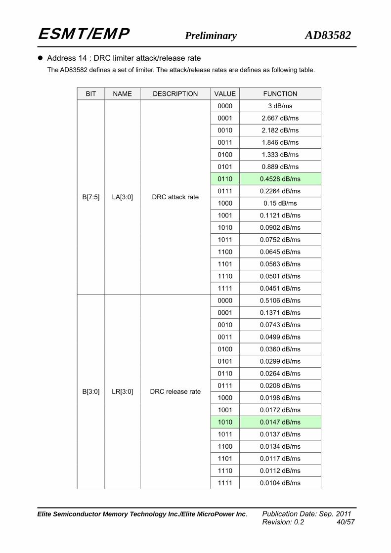
Address 14 : DRC limiter attack/release rate The AD83582 defines a set of limiter. The attack/release rates are defines as following table.
BIT NAME DESCRIPTION VALUE FUNCTION
0000 3 dB/ms
0001 2.667 dB/ms
0010 2.182 dB/ms
0011 1.846 dB/ms
0100 1.333 dB/ms
0101 0.889 dB/ms
0110 0.4528 dB/ms
0111 0.2264 dB/ms
1000 0.15 dB/ms
1001 0.1121 dB/ms
1010 0.0902 dB/ms
1011 0.0752 dB/ms
1100 0.0645 dB/ms
1101 0.0563 dB/ms
1110 0.0501 dB/ms
B[7:5] LA[3:0] DRC attack rate
1111 0.0451 dB/ms
0000 0.5106 dB/ms
0001 0.1371 dB/ms
0010 0.0743 dB/ms
0011 0.0499 dB/ms
0100 0.0360 dB/ms
0101 0.0299 dB/ms
0110 0.0264 dB/ms
0111 0.0208 dB/ms
1000 0.0198 dB/ms
1001 0.0172 dB/ms
1010 0.0147 dB/ms
1011 0.0137 dB/ms
1100 0.0134 dB/ms
1101 0.0117 dB/ms
1110 0.0112 dB/ms
B[3:0] LR[3:0] DRC release rate
1111 0.0104 dB/ms
ESMT/EMP Preliminary AD83582
Elite Semiconductor Memory Technology Inc./Elite MicroPower Inc. Publication Date: Sep. 2011 Revision: 0.2 41/57
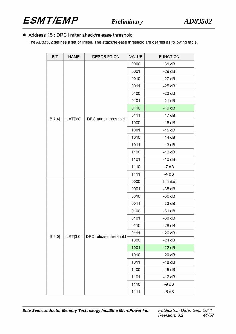
Address 15 : DRC limiter attack/release threshold The AD83582 defines a set of limiter. The attack/release threshold are defines as following table.
BIT NAME DESCRIPTION VALUE FUNCTION
0000 -31 dB
0001 -29 dB
0010 -27 dB
0011 -25 dB
0100 -23 dB
0101 -21 dB
0110 -19 dB
0111 -17 dB
1000 -16 dB
1001 -15 dB
1010 -14 dB
1011 -13 dB
1100 -12 dB
1101 -10 dB
1110 -7 dB
B[7:4] LAT[3:0] DRC attack threshold
1111 -4 dB
0000 Infinite
0001 -38 dB
0010 -36 dB
0011 -33 dB
0100 -31 dB
0101 -30 dB
0110 -28 dB
0111 -26 dB
1000 -24 dB
1001 -22 dB
1010 -20 dB
1011 -18 dB
1100 -15 dB
1101 -12 dB
1110 -9 dB
B[3:0] LRT[3:0] DRC release threshold
1111 -6 dB
ESMT/EMP Preliminary AD83582
Elite Semiconductor Memory Technology Inc./Elite MicroPower Inc. Publication Date: Sep. 2011 Revision: 0.2 42/57
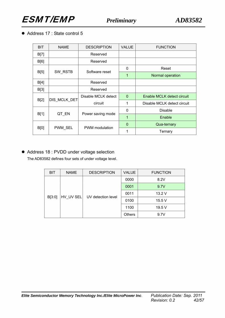
Address 17 : State control 5
BIT NAME DESCRIPTION VALUE FUNCTION
B[7] Reserved
B[6] Reserved
0 Reset B[5] SW_RSTB Software reset
1 Normal operation
B[4] Reserved
B[3] Reserved
0 Enable MCLK detect circuit B[2] DIS_MCLK_DET
Disable MCLK detect
circuit 1 Disable MCLK detect circuit
0 Disable B[1] QT_EN Power saving mode
1 Enable
0 Qua-ternary B[0] PWM_SEL PWM modulation
1 Ternary
Address 18 : PVDD under voltage selection The AD83582 defines four sets of under voltage level.
BIT NAME DESCRIPTION VALUE FUNCTION
0000 8.2V
0001 9.7V
0011 13.2 V
0100 15.5 V
1100 19.5 V
B[3:0] HV_UV SEL UV detection level
Others 9.7V

ESMT/EMP Preliminary AD83582
Elite Semiconductor Memory Technology Inc./Elite MicroPower Inc. Publication Date: Sep. 2011 Revision: 0.2 43/57
Address 19 : Zero detection level selection This register is to define zero detection level selection.
BIT NAME DESCRIPTION VALUE FUNCTION
B[7] Reserved
B[6] Reserved
B[5] Reserved
B[4] Reserved
00 signal = 0
01 signal <-110dB
10 Signal < -100dB B[3:2] ZD_LEVEL[1:0] Zero detection level
11 Signal < -90dB
00 x1/8
01 x1/4
10 x1/2 B[1:0] ZD_GAIN[1:0]
Zero detection gain
level
11 Mute
Address 20~36 : User-defined coefficients registers An on-chip RAM in AD83582 stores user-defined EQ and mixing coefficients. The content of this coefficient
RAM is indirectly accessed via coefficient registers, which consist of one base address register (address 20),
five sets of registers (address 21 to 35) of three consecutive 8-bit entries for each 24-bit coefficient, and one
control register (address 36) to control access of the coefficients in the RAM..
Address 20 BIT NAME DESCRIPTION VALUE FUNCTION
B[7] Reserved
B[6:0] CFA[6:0] Coefficient RAM base
address 0000000
Address 21, A1cf1 BIT NAME DESCRIPTION VALUE FUNCTION
B[7:0] C1B[23:16] Top 8-bits of
coefficients A1

ESMT/EMP Preliminary AD83582
Elite Semiconductor Memory Technology Inc./Elite MicroPower Inc. Publication Date: Sep. 2011 Revision: 0.2 44/57
Address 22, A1cf2
BIT NAME DESCRIPTION VALUE FUNCTION
B[7:0] C1B[15:8] Middle 8-bits of
coefficients A1
Address 23, A1cf3 BIT NAME DESCRIPTION VALUE FUNCTION
B[7:0] C1B[23:16] Bottom 8-bits of
coefficients A1
Address 24, A2cf1 BIT NAME DESCRIPTION VALUE FUNCTION
B[7:0] C2B[23:16] Top 8-bits of
coefficients A2
Address 25, A2cf2 BIT NAME DESCRIPTION VALUE FUNCTION
B[7:0] C2B[15:8] Middle 8-bits of
coefficients A2
Address 26, A2cf3 BIT NAME DESCRIPTION VALUE FUNCTION
B[7:0] C2B[7:0] Bottom 8-bits of
coefficients A2
Address 27, B1cf1 BIT NAME DESCRIPTION VALUE FUNCTION
B[7:0] C3B[23:16] Top 8-bits of
coefficients B1
Address 28, B1cf2 BIT NAME DESCRIPTION VALUE FUNCTION
B[7:0] C3B[15:8] Middle 8-bits of
coefficients B1

ESMT/EMP Preliminary AD83582
Elite Semiconductor Memory Technology Inc./Elite MicroPower Inc. Publication Date: Sep. 2011 Revision: 0.2 45/57
Address 29, B1cf3 BIT NAME DESCRIPTION VALUE FUNCTION
B[7:0] C3B[7:0] Bottom 8-bits of
coefficients B1
Address 30, B2cf1 BIT NAME DESCRIPTION VALUE FUNCTION
B[7:0] C4B[23:16] Top 8-bits of
coefficients B2
Address 31, B2cf2 BIT NAME DESCRIPTION VALUE FUNCTION
B[7:0] C4B[15:8] Middle 8-bits of
coefficients B2
Address 32, B2cf3 BIT NAME DESCRIPTION VALUE FUNCTION
B[7:0] C4B[7:0] Bottom 8-bits of
coefficients B2
Address 33, A0cf1 BIT NAME DESCRIPTION VALUE FUNCTION
B[7:0] C5B[23:16] Top 8-bits of
coefficients A0
Address 34, A0cf2 BIT NAME DESCRIPTION VALUE FUNCTION
B[7:0] C5B[15:8] Middle 8-bits of
coefficients A0
Address 35, A0cf3 BIT NAME DESCRIPTION VALUE FUNCTION
B[7:0] C5B[7:0] Bottom 8-bits of
coefficients A0

ESMT/EMP Preliminary AD83582
Elite Semiconductor Memory Technology Inc./Elite MicroPower Inc. Publication Date: Sep. 2011 Revision: 0.2 46/57
Address 36, CfRW BIT NAME DESCRIPTION VALUE FUNCTION
B[7:4] Reserved
0 Read complete B[3] RA
Enable of reading a set of
coefficients from RAM 1 Read enable
0 Read complete B[2] R1
Enable of reading a single
coefficients from RAM 1 Read enable
0 Write complete B[1] WA
Enable of writing a set of
coefficients to RAM 1 Write enable
0 Write complete B[0] W1
Enable of writing a single
coefficient to RAM 1 Write enable

ESMT/EMP Preliminary AD83582
Elite Semiconductor Memory Technology Inc./Elite MicroPower Inc. Publication Date: Sep. 2011 Revision: 0.2 47/57
Address 42 : Power saving mode switching level If the PWM exceeds the programmed switching power level (default 26*40ns), the modulation algorithm will
change from quaternary into power saving mode. It results in higher power efficiency during larger power
output operations. If the PWM drops below the programmed switching power level, the modulation algorithm
will change back to quaternary modulation.
BIT NAME DESCRIPTION VALUE FUNCTION
B[7] Reserved
B[6] Reserved
B[5] Reserved
11111 62
11110 60
: :
01111 30
01110 28
01101 26
: :
00010 4
00001 4
B[4:0] QT_SW_LEVEL Switching level
00000 4
Total Harmonic Distortion + Noise vs. Output Power
0.04
2
0.060.08
0.2
0.3
0.5
0.7
1
%
2 203 4 5 6 7 8 9 10W
Quaternary Switching level 20 Switching level 30 Switching level 40 Switching level 46
24V, 8Ω

ESMT/EMP Preliminary AD83582
Elite Semiconductor Memory Technology Inc./Elite MicroPower Inc. Publication Date: Sep. 2011 Revision: 0.2 48/57
The procedure to read/write coefficient(s) from/to RAM is as followings:
Read a single coefficient from RAM:
1. Write 7-bis of address to I2C address-20
2. Write 1 to R1 bit in address-36
3. Read top 8-bits of coefficient in I2C address-21
4. Read middle 8-bits of coefficient in I2C address-22
5. Read bottom 8-bits of coefficient in I2C address-23
Read a set of coefficients from RAM:
1. Write 7-bits of address to I2C address-20
2. Write 1 to RA bit in address-36
3. Read top 8-bits of coefficient in I2C address-21
4. Read middle 8-bits of coefficient in I2C address-22
5. Read bottom 8-bits of coefficient in I2C address-23
6. Read top 8-bits of coefficient A2 in I2C address-24
7. Read middle 8-bits of coefficient A2 in I2C address-25
8. Read bottom 8-bits of coefficient A2 in I2C address-26
9. Read top 8-bits of coefficient B1 in I2C address-27
10. Read middle 8-bits of coefficient B1 in I2C address-28
11. Read bottom 8-bits of coefficient B1 in I2C address-29
12. Read top 8-bits of coefficient B2 in I2C address-30
13. Read middle 8-bits of coefficient B2 in I2C address-31
14. Read bottom 8-bits of coefficient B2 in I2C address-32
15. Read top 8-bits of coefficient A0 in I2C address-33
16. Read middle 8-bits of coefficient A0 in I2C address-34
17. Read bottom 8-bits of coefficient A0 in I2C address-35
Write a single coefficient from RAM:
1. Write 7-bis of address to I2C address-20
2. Write top 8-bits of coefficient in I2C address-21
3. Write middle 8-bits of coefficient in I2C address-22
4. Write bottom 8-bits of coefficient in I2C address-23
5. Write 1 to W1 bit in address-36

ESMT/EMP Preliminary AD83582
Elite Semiconductor Memory Technology Inc./Elite MicroPower Inc. Publication Date: Sep. 2011 Revision: 0.2 49/57
Write a set of coefficients from RAM:
1. Write 7-bits of address to I2C address-20
2. Write top 8-bits of coefficient in I2C address-21
3. Write middle 8-bits of coefficient in I2C address-22
4. Write bottom 8-bits of coefficient in I2C address-23
5. Write top 8-bits of coefficient A2 in I2C address-24
6. Write middle 8-bits of coefficient A2 in I2C address-25
7. Write bottom 8-bits of coefficient A2 in I2C address-26
8. Write top 8-bits of coefficient B1 in I2C address-27
9. Write middle 8-bits of coefficient B1 in I2C address-28
10. Write bottom 8-bits of coefficient B1 in I2C address-29
11. Write top 8-bits of coefficient B2 in I2C address-30
12. Write middle 8-bits of coefficient B2 in I2C address-31
13. Write bottom 8-bits of coefficient B2 in I2C address-32
14. Write top 8-bits of coefficient A0 in I2C address-33
15. Write middle 8-bits of coefficient A0 in I2C address-34
16. Write bottom 8-bits of coefficient A0 in I2C address-35
17. Write 1 to WA bit in address-36
Note that: the read and write operation on RAM coefficients works only if LRCIN (pin-15) switching on rising
edge. And, before each writing operation, it is necessary to read the address-36 to confirm whether RAM is
writable current in first. If the logic of W1 or WA is high, the coefficient writing is prohibited.

ESMT/EMP Preliminary AD83582
Elite Semiconductor Memory Technology Inc./Elite MicroPower Inc. Publication Date: Sep. 2011 Revision: 0.2 50/57
User-defined equalizer The AD83582 has built-in 8-bands parametric EQ for each channel. Each EQ, Users can program suitable
coefficients via I2C control interface to get the required audio band frequency response. The transfer
function of EQ is:
The data format of 2’s complement binary code for EQ coefficient is 4.20. i.e., 4-bits for integer (MSB is sign
bit) and 20-bits for mantissa. The each coefficient range is from 0x800000 (-8) to 0x7FFFFF
(+7.999999046325684). These coefficients are stored in User Defined RAM and are referenced in following
manner:
where x and y represents the number of channel and the band number of EQ biquard respectively.
By default, all user-defined filters are path-through where all coefficients are set to 0, except the A0 is set to
0x100000 (represents 1).
Mixer The AD83582 provides mixers to generate the extra audio source from input left/right channels. The
coefficients of mixers are defined in range from 0x800000 (-1) to 0x7FFFFF (0.9999998808). The function
block diagram is as following:
M12
M11
M22
M21
M32
M31
LCH
RCH
SUB
L
R
22
11
22
110
1)( −−
−−
++++
=zBzBzAzAAzH
2211
221100
BCHxEQyBBCHxEQyB
ACHxEQyAACHxEQyAACHxEQyA
−=−=
===
ESMT/EMP Preliminary AD83582
Elite Semiconductor Memory Technology Inc./Elite MicroPower Inc. Publication Date: Sep. 2011 Revision: 0.2 51/57
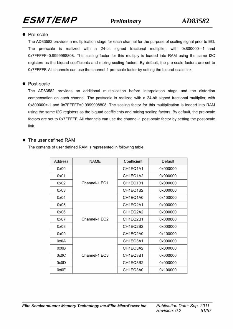
Pre-scale The AD83582 provides a multiplication stage for each channel for the purpose of scaling signal prior to EQ.
The pre-scale is realized with a 24-bit signed fractional multiplier, with 0x800000=-1 and
0x7FFFFF=0.9999998808. The scaling factor for this multiply is loaded into RAM using the same I2C
registers as the biquad coefficients and mixing scaling factors. By default, the pre-scale factors are set to
0x7FFFFF. All channels can use the channel-1 pre-scale factor by setting the biquad-scale link.
Post-scale The AD83582 provides an additional multiplication before interpolation stage and the distortion
compensation on each channel. The postscale is realized with a 24-bit signed fractional multiplier, with
0x800000=-1 and 0x7FFFFF=0.9999998808. The scaling factor for this multiplication is loaded into RAM
using the same I2C registers as the biquad coefficients and mixing scaling factors. By default, the pre-scale
factors are set to 0x7FFFFF. All channels can use the channel-1 post-scale factor by setting the post-scale
link.
The user defined RAM The contents of user defined RAM is represented in following table.
Address NAME Coefficient Default
0x00 CH1EQ1A1 0x000000
0x01 CH1EQ1A2 0x000000
0x02 CH1EQ1B1 0x000000
0x03 CH1EQ1B2 0x000000
0x04
Channel-1 EQ1
CH1EQ1A0 0x100000
0x05 CH1EQ2A1 0x000000
0x06 CH1EQ2A2 0x000000
0x07 CH1EQ2B1 0x000000
0x08 CH1EQ2B2 0x000000
0x09
Channel-1 EQ2
CH1EQ2A0 0x100000
0x0A CH1EQ3A1 0x000000
0x0B CH1EQ3A2 0x000000
0x0C CH1EQ3B1 0x000000
0x0D CH1EQ3B2 0x000000
0x0E
Channel-1 EQ3
CH1EQ3A0 0x100000

ESMT/EMP Preliminary AD83582
Elite Semiconductor Memory Technology Inc./Elite MicroPower Inc. Publication Date: Sep. 2011 Revision: 0.2 52/57
Address NAME Coefficient Default
0x0F CH1EQ4A1 0x000000
0x10 CH1EQ4A2 0x000000
0x11 CH1EQ4B1 0x000000
0x12 CH1EQ4B2 0x000000
0x13
Channel-1 EQ4
CH1EQ4A0 0x100000
0x14 CH1EQ5A1 0x000000
0x15 CH1EQ5A2 0x000000
0x16 CH1EQ5B1 0x000000
0x17 CH1EQ5B2 0x000000
0x18
Channel-1 EQ5
CH1EQ5A0 0x100000
0x19 CH1EQ6A1 0x000000
0x1A CH1EQ6A2 0x000000
0x1B CH1EQ6B1 0x000000
0x1C CH1EQ6B2 0x000000
0x1D
Channel-1 EQ6
CH1EQ6A0 0x100000
0x1E CH1EQ7A1 0x000000
0x1F CH1EQ7A2 0x000000
0x20 CH1EQ7B1 0x000000
0x21 CH1EQ7B2 0x000000
0x22
Channel-1 EQ7
CH1EQ7A0 0x100000
0x23 CH1EQ8A1 0x000000
0x24 CH1EQ8A2 0x000000
0x25 CH1EQ8B1 0x000000
0x26 CH1EQ8B2 0x000000
0x27
Channel-1 EQ8
CH1EQ8A0 0x100000
0x28 Reserved
0x29 Reserved
0x2A Reserved
0x3B Reserved
0x2C Reserved

ESMT/EMP Preliminary AD83582
Elite Semiconductor Memory Technology Inc./Elite MicroPower Inc. Publication Date: Sep. 2011 Revision: 0.2 53/57
Address NAME Coefficient Default
0x2D CH2EQ1A1 0x000000
0x2E CH2EQ1A2 0x000000
0x2F CH2EQ1B1 0x000000
0x30 CH2EQ1B2 0x000000
0x31
Channel-2 EQ1
CH2EQ1A0 0x100000
0x32 CH2EQ2A1 0x000000
0x33 CH2EQ2A2 0x000000
0x34 CH2EQ2B1 0x000000
0x35 CH2EQ2B2 0x000000
0x36
Channel-2 EQ2
CH2EQ2A0 0x100000
0x37 CH2EQ3A1 0x000000
0x38 CH2EQ3A2 0x000000
0x39 CH2EQ3B1 0x000000
0x3A CH2EQ3B2 0x000000
0x3B
Channel-2 EQ3
CH2EQ3A0 0x100000
0x3C CH2EQ4A1 0x000000
0x3D CH2EQ4A2 0x000000
0x3E CH2EQ4B1 0x000000
0x3F CH2EQ4B2 0x000000
0x40
Channel-2 EQ4
CH2EQ4A0 0x100000
0x41 CH2EQ5A1 0x000000
0x42 CH2EQ5A2 0x000000
0x43 CH2EQ5B1 0x000000
0x44 CH2EQ5B2 0x000000
0x45
Channel-2 EQ5
CH2EQ5A0 0x100000
0x46 CH2EQ6A1 0x000000
0x47 CH2EQ6A2 0x000000
0x48 CH2EQ6B1 0x000000
0x49 CH2EQ6B2 0x000000
0x4A
Channel-2 EQ6
CH2EQ6A0 0x100000

ESMT/EMP Preliminary AD83582
Elite Semiconductor Memory Technology Inc./Elite MicroPower Inc. Publication Date: Sep. 2011 Revision: 0.2 54/57
Address NAME Coefficient Default
0x4B CH2EQ7A1 0x000000
0x4C CH2EQ7A2 0x000000
0x4D CH2EQ7B1 0x000000
0x4E CH2EQ7B2 0x000000
0x4F
Channel-2 EQ7
CH2EQ7A0 0x100000
0x50 CH2EQ8A1 0x000000
0x51 CH2EQ8A2 0x000000
0x52 CH2EQ8B1 0x000000
0x53 CH2EQ8B2 0x000000
0x54
Channel-2 EQ8
CH2EQ8A0 0x100000
0x55 Reserved
0x56 Reserved
0x57 Reserved
0x58 Reserved
0x59 Reserved
0x5A Channel-1 Mixer1 M11 0x7FFFFF
0x5B Channel-1 Mixer2 M12 0x000000
0x5C Channel-2 Mixer1 M21 0x000000
0x5D Channel-2 Mixer2 M22 0x7FFFFF
0x5E Channel-3 Mixer1 M31 0x400000
0x5F Channel-3 Mixer2 M32 0x400000
0x60 Channel-1 Prescale C1PRS 0x7FFFFF
0x61 Channel-2 Prescale C2PRS 0x7FFFFF
0x62 Channel-1 Postscale C1POS 0x7FFFFF
0x63 Channel-2 Postscale C2POS 0x7FFFFF
0x64 Channel-3 Postscale C3POS 0x7FFFFF
0x65 Channel-1 Power
clipping PC1 0x200000
0x66 Channel-2 Power
clipping PC2 0x200000
0x67 Channel-3 Power
clipping PC3 0x200000

ESMT/EMP Preliminary AD83582
Elite Semiconductor Memory Technology Inc./Elite MicroPower Inc. Publication Date: Sep. 2011 Revision: 0.2 55/57
Package Dimensions 7mm x 7mm 48-pin E-LQFP
b
D2
E2
e
D1
D
E1
E
DIMENSIONS IN MILLIMETERSSymbols
MIN. NOM. MAX.
A 1.60
A1 0.05 0.15
b 0.17 0.22 0.27
D 9.00 BSC
D1 7.00 BSC
D2 4.5 5.0 5.5
E 9.00 BSC
E1 7.00 BSC
E2 4.5 5.0 5.5
e 0.50 BSC
L 0.45 0.60 0.75
L1 1.00 BSC
θ 0° 3.5° 7°
A
A1
Θ
L1L

ESMT/EMP Preliminary AD83582
Elite Semiconductor Memory Technology Inc./Elite MicroPower Inc. Publication Date: Sep. 2011 Revision: 0.2 56/57
Revision History
Revision Date Description
0.1 2011.06.09 Original
0.2 2011.09.26
1) Changed PVDD range from 12V~24V to 10V~26V. 2) Changed PVDD absolute maximum rating from 26V to
30V. 3) Updated the application circuit that the snubber circuit
can be removed while the PVDD <=18V for stereo. 4) Added the application circuit for economic type,
moderate EMI suppression. 5) Added power on sequence flow. 6) Updated MPQ description.
ESMT/EMP Preliminary AD83582
Elite Semiconductor Memory Technology Inc./Elite MicroPower Inc. Publication Date: Sep. 2011 Revision: 0.2 57/57
Important Notice All rights reserved. No part of this document may be reproduced or duplicated in any form or by any means without the prior permission of ESMT. The contents contained in this document are believed to be accurate at the time of publication. ESMT assumes no responsibility for any error in this document, and reserves the right to change the products or specification in this document without notice. The information contained herein is presented only as a guide or examples for the application of our products. No responsibility is assumed by ESMT for any infringement of patents, copyrights, or other intellectual property rights of third parties which may result from its use. No license, either express , implied or otherwise, is granted under any patents, copyrights or other intellectual property rights of ESMT or others. Any semiconductor devices may have inherently a certain rate of failure. To minimize risks associated with customer's application, adequate design and operating safeguards against injury, damage, or loss from such failure, should be provided by the customer when making application designs. ESMT's products are not authorized for use in critical applications such as, but not limited to, life support devices or system, where failure or abnormal operation may directly affect human lives or cause physical injury or property damage. If products described here are to be used for such kinds of application, purchaser must do its own quality assurance testing appropriate to such applications.