european roadmap on superconductor electronics · european roadmap on superconductor electronics,...
TRANSCRIPT

European Roadmap
on
Superconductor Electronics
Status and Perspectives
Edited by
H.-G. Meyer, J. Niemeyer, and H. Rogalla
Version June 2010
Deliverable of European Project S-PULSE (FP7-215297)

European Roadmap on Superconductor Electronics, Version June 2010
Contents
List of Authors 1
Executive Summary 2
1. Society needs and vision, industrial impact 3
2. Basics of Superconductor Electronics 11
3. Application of Superconductor Electronics
3.1 Radiation Detectors 18
3.2 Digital Electronics 27
3.3 Magnetic Field Sensors 37
3.4 Fundamental Metrology 46
3.5 Artificial Atoms 52
3.6 Passive Microwave Devices 54
4. Materials and Fabrication Technology for Superconductor Electronics 55
5. Enabling Technologies 68
6. European SE Research Vision 80
Acknowledgements 87
1

European Roadmap on Superconductor Electronics, Version June 2010
1
List of Authors
Anders, S. IPHT, Jena, Germany Blamire, M. Univ. Cambridge, United Kingdom Buchholz, F.-Im. PTB, Braunschweig, Germany Crete, D. THALES Research and Technology, Paris, France Cristiano, R. CNR, Italy Febvre, P. Univ. Savoie, France
IPHT, Jena, Germany Fritzsch, L. Herr, A. Univ. Chalmers, Sweden Ili’chev, E. IPHT, Jena, Germany Kohlmann, J. PTB, Braunschweig, Germany
IPHT, Jena, Germany Kunert, J. Meyer, H.-G. IPHT, Jena, Germany Niemeyer, J. PTB, Braunschweig, Germany Ortlepp, T. Univ. Ilmenau, Germany Rogalla, H. Univ. Twente, The Netherlands Schurig, T. PTB, Berlin, Germany Siegel, M. Univ. Karlsruhe, Germany
IPHT, Jena, Germany Stolz, R. Tarte, E. Univ. Birmingham, United Kingdom Ter Brake, M. Univ. Twente, The Netherlands Töpfer, H. Univ. Ilmenau, Germany Villegier, J.-C. CEA, Grenoble, France Zagorskin, A.M. Univ. British Columbia, Canada Zorin, A.B PTB, Braunschweig, Germany
1
Executive Summary 2
Executive Summary
For four decades semiconductor electronics has followed Moore's law: with each generation of integration the circuit features became smaller, more complex and faster. This development is now reaching a wall so that smaller is no longer any faster. The clock-rate has saturated at about 3 to 5 GHz and the parallel processor approach will soon reach its limit. The prime reason for the limitation the semiconductor electronics experiences is not the switching speed of the individual transistor, but its power dissipation and thus heat.
Digital Superconductive Electronics is a circuit- and device-technology that is inherently faster at much less power dissipation than semiconductor electronics. It makes use of superconductors and Josephson junctions as circuit elements, which can provide extremely fast digital devices in a frequency range – dependent on the material – of hundreds of GHz: for example a flip-flop has been demonstrated that operated at 750 GHz. This digital technique is scalable and follows similar design rules as semiconductor devices. Its very low power dissipation of only 0.1 µWatt per gate at 100 GHz opens the possibility of three dimensional integration. Circuits like microprocessors and analog-to-digital converters for commercial and military applications have been demonstrated. In contrast to semiconductor circuits, the operation of superconducting circuits is based on naturally standardized digital pulses the area of which is exactly the flux quantum Φ0. The flux quantum is also the natural quantization unit for digital-to-analog and analog-to-digital converters. The latter application is so precise, that it is being used as voltage standard and that the physical unit 'Volt' is defined by means of this standard.
Apart from its outstanding features for digital electronics, Superconductive Electronics provides also the most sensitive sensor for magnetic fields: the Superconducting Quantum Interference Device (SQUID). Amongst many other applications SQUIDs are used as sensors for magnetic heart and brain signals in medical applications, as sensor for geological surveying and food-processing and for non-destructive testing. As amplifiers of electrical signals, SQUIDs can nearly reach the theoretical limit given by Quantum Mechanics.
A further important field of application is the detection of very week signals by 'transition-edge' bolometers and superconductive tunnel junctions. Their application as radiation detectors in a wide frequency range, from microwaves to x-rays is now standard. The very low losses of superconductors have led to commercial microwave filter designs that are now widely used in the USA in base-stations for cellular phones and in military communication applications. The number of demonstrated applications is continuously increasing and there is no area in professional electronics, in which Superconductive Electronics cannot be applied and surpasses the performance of classical devices.
Superconductive Electronics has to be cooled to very low temperatures. Whereas this was a bottleneck in the past, cooling techniques have made a huge step forward in recent years: very compact systems with high reliability and a wide range of cooling power are available commercially, from microcoolers of match-box size with milli-Watt cooling power to high-reliability coolers of many Watts of cooling power for satellite applications. Superconductive Electronics will not replace semiconductor electronics and similar room-temperature techniques in standard applications, but for those applications which require very high speed, low power consumption, extreme sensitivity or extremely high precision, Superconductive Electronics is superior to all other available techniques.
To strengthen the European competitiveness in superconductor electronics research projects have to be set-up in the following field: - Ultra-sensitive sensing and imaging, - Quantum measurement instrumentation, - Advanced analog-to-digital converters, - Superconductive electronics technology.

European Roadmap on Superconductor Electronics, Version June 2010 3
1. Social and economic impact of superconductive electronics
1.1. Society Needs and Vision
After a century of unlimited resources and dramatic successes of science and technology, which resulted in fundamental changes in practically all societies of the world, we are now approaching limitations on a number of fronts:
The freedom of the individual is counterbalanced more and more by the need of the society for security against international crime and global terrorism.
The big ‘old’ industrial countries face serious technological and economical competition from emerging markets.
Fossil energy sources are becoming rarer and less accepted because of the CO2-related danger of global warming.
Alternative energies like solar power are not yet available to a sufficient degree in most industrial societies, but are especially productive in areas of more or less political instability.
The growth of the information infrastructure and processing power for our information based society is slowing down because of speed limitations of computers and data networks and the increasing immense investment costs for faster and faster technologies.
Moore’s law and the rule ‘smaller is faster’ dominated the semiconductor industry in the last decennia and are breaking down now.
The globalization of research, industrial production, and trade require to a high degree uniformity of measures and measuring instrumentation.
This list is far from complete. It covers social and industrial aspects as well as scientific and technological developments. In the technical sector one can observe three major developments: higher speed (or equivalently larger bandwidth), better sensitivity of instrumentation, the demand of ever less invasive techniques and in the social sector there is an increasing pressure towards environmental compatibility and sustainable energy and resources.
Although these developments are not yet deeply interwoven, political and economical pressure will very likely enforce their fusion in the next decennia.
To solve these problems, many techniques developed in the last 100 years will play an increasingly important role in the future. Superconductivity is one of them. Found in 1911 by Kammerling Onnes it has seen an incredible development since then. Not only has the maximum temperature below which one finds electronic transport without resistance been increased from 4.3K in mercury to more than 150K in ceramic materials, but also many new effects have been found, such as the quantization of magnetic flux in superconducting topologies, the Josephson effect, d-wave superconductivity, superconductivity in ceramics, interface of different oxides and exotic materials, for which the mechanism leading to superconductivity is not yet understood, non-equilibrium superconductivity and many more. All these effects have resulted in techniques that can be applied to electronics and led to new electronic devices – in analogue electronics as well as in digital electronics. Superconductive electronics often plays the role of a pathfinder for new electronic applications. In many cases there is no competitive alternative in conventional electronics.
Superconducting devices need cooling to quite low temperatures. For practical applications cooling with liquid helium is not adequate because the handling is too error prone. In the last decade a lot of progress has been made with cryocoolers in terms of reliability and ease of operation. These cooling devices are available in a wide range of cooling powers, temperatures and reliabilities. They are already adequate for cooling the majority of current applications. Nevertheless, a lot needs still to be done in this area to meet the need of the society for energy efficiency: whereas cryocoolers for large cooling power are quite close to the theoretically predicted efficiency, coolers with small cooling power only reach an unacceptable low efficiency of a few percent of the theoretical value. Improvement in this area would also help to meet expectations in the superconducting electronics concerning size and integration into existing frame works, e.g. of the telecommunication industry.

1. Social and economic impact of superconductive electronics 4
Superconducting electronics can already now contribute significantly to the needs of our society. It has the potential to play a major role as a key technology in the future. The realization is primarily dependent on the investment society will make in this technology and not on the performance of this technology itself. Some fields where superconductive electronics is covering or will cover important society needs are described in the following part:
1.1.1. Resources and Environment (Energy awareness, geophysical prospection and access to natural resources)
Superconductive Interference Device (SQUID) Gradiometers with their relatively large sampling rate and high sensitivity enable airborne mapping of extended magnetic structures on the surface of the earth for the detection of raw material reservoirs. Similar systems have proven very useful in finding extended archeological structures. Successful tests of intrinsic planar full-tensor LTS (low-temperature superconductor) SQUID gradiometers were conducted by towing the system from a helicopter as well as for a stinger-mounted configuration in a Cessna 208 aircraft.
By measuring both the component of the magnetic field parallel to the surface and the resistivity of the surface, the impedance of the earth’s surface can be determined with a SQUID sensor, valuable information can be obtained for the detection of environmental problem sites, the exploration of ground water resources, the analysis of construction sites etc.
Superconductive AC voltage synthesizers can be used to test and calibrate the low frequency (5 - 40 Hz) seismic equipment for petroleum and natural gas detection, for the exploration of geothermal energy, and for providing large scale surveys of the earth crust to minimize hazards by earthquake prediction. The most important technical specification of these instruments is their nonlinear distortion of harmonic signals. For the inharmonic content typical values of 0.0005% are given. Up to now there is no legal measuring tool to prove such values. Only superconductive quantum AC synthesizers would be able to calibrate such instruments and improve the geophysical signal analysis.
As the superconducting systems for geophysical exploration are more sensitive and faster than conventional coil systems or even without any conventional competitor, they will enable to detect new hidden repositories of minerals. With the increasing demand for natural resources this will be of great economic relevance.
1.1.2. Security and mobility Mobility is the key requirement for a global
society, and at the same time it is one of their megatrends. People travel around the world, and they do exchange ideas, goods, and services. cross-border transportation is a boom market: for example European air traffic grows 5.2% every year resulting in a doubling of throughput by 2025.
This liberty is jeopardised by the menace of international terrorism. Mobility is nothing without the guarantee of security. Admittedly, these two basic social values – mobility and security – are not fully compatible. Security screening measures interfere with a person’s privacy, so they are commonly disliked and mistrusted. Moreover, some existing security technologies like x-ray or active millimetre wave scanner, disregard not only privacy, but also health. From an economic point of view, keeping a secure travel means high costs (technology and personnel) and a loss of valuable time.
The market of products for security applications is booming since the 9/11 disaster. Growth rate around 30% are predicted by market analysts. E.g. products for biometry and forensic amounts to 1.8 billion US$ in 2007 (BBC research), and instruments for the screening of persons are predicted to amount to 1.85 billion US$ in 2010 (“2003 -2010 Industry Market & Products Report”, Security Research Corp. 2004). These two fields value over 20 billion US$ in 2015.
International security research has originated a lot of promising technologies, which are already in use at some places. The concept of personal screening using x-rays is not acceptable for health reasons, although it provides excellent results. So, the typical screening procedure remains as it is: metal detectors (which obviously can not detect non-metallic hazards like ceramic knifes) in combination with manual scanning. The recently developed millimetre wave imagers already pose a considerable advantage, although their performance is already at the limit

European Roadmap on Superconductor Electronics, Version June 2010 5
since they are based on conventional microwave technology. Typically they lack sensitivity for indoor operation, which restricts their use to cabins with artificial signal enhancement.
As its successor, superconducting technology will allow to improve these portals. As already demonstrated they will result in terahertz cameras, which can be deployed in various environments. The heart of such cameras is a superconducting detector, which allows to passively record terahertz emissions at video rates. This spectral range contains a variety of information about the person being investigated (hazardous materials, hidden objects etc.). Because of the very weak signals, passive mode makes huge demands on the detector which only can be achieved by superconductor technology. In the next few years superconductive terahertz cameras with video frame rate will be one major target for further research and development.
Carry-on luggage control is another similar example. Conventional systems are based on x-ray imaging. They can display only the shape of the packed objects whereas the recent SQUID-based low filed NMR scanner allows simultaneously both imaging of objects and identification of substances contained inside bottles, aerosol cans, cream jars etc. This is a groundbreaking new technology for airport security. First such systems are already under test at airports in the US. Europe with its overwhelming lead in SQUID technology could and should definitely target this security market.
1.1.3. Information and production In the current era of the Internet ”explosion” and
the convergence of different communication services (for example, global wide-area-networks, wireless communication, and digital multimedia) the most serious concerns of society are quality of service, unification of interfaces and communication security. These three factors taken together place an enormous pressure on the development of electronic systems.
In the field of conventional digital electronics, the ‘need for speed’ and the ever-decreasing energy per bit/second has reached a limit. Integrated processors with a complexity of some 106 transistors per chip are limited to processor clock-frequencies of a few Gigahertz. Even slightly higher clock rates would require major investments in cooling. Clock rates of
50GHz or higher seem to be impossible for complex circuits. The industry has found an intermediate solution in putting more processors on a chip, which allows for parallel processing of information. This technique will again hit a limit when the overhead for the organization of the parallel processing takes a significant proportion of the processing power. Such a slow down is already expected for 16 parallel processors. In addition software verification becomes nearly impossible in real-time applications. A number of the limitations of semiconductor digital electronics can be overcome by superconducting digital electronics. A major advantage is the much lower switching energy by about 4 orders of magnitude combined with an intrinsic switching delay of picoseconds or even less. Superconducting electronics can supply digital circuits as well as analogue circuits and interfaces. Analogue-to-digital and digital-to-analogue converters have the potential to outperform the equivalent semiconductor circuits in speed, accuracy (they have a built-in natural quantum standard) and power consumption. Also interfacing to devices for quantum computing (qubits) and ultra-sensitive magnetic sensors (SQUIDs) can be realized in a natural way. In combination with much slower, but higher integration semiconductor techniques and optical techniques for the data transfer, the superconducting digital electronics has all ingredients to meet the needs of a future society for computational speed and integration density at low energy consumption and at limited software complexity.
To support and improve production processes, extremely sensitive superconductive magnetometers or magnetometer arrays are very useful for non-destructive evaluation of safety relevant metal parts like airplane wheels, rivet joints at airplanes or construction parts like steel enforcement in bridges and buildings. Such instruments permit the characterization of small, irregular-shaped stainless steel samples containing pinch welds as well as the analysis of the current flow in solar cells. SQUIDS may detect smaller failures and production problems in an earlier state. Facing the enormous costs of a breakdown of a safety relevant part or failures in a mass production process, it would be very cost effective to use superconductive electronics for preventing such events.

1. Social and economic impact of superconductive electronics 6
1.1.4. Food security and health care Sensitive SQUID magnetometers are able to detect
impurities in food during production or packaging without interrupting the manufacturing processes or opening the packages.
Another area of technological development in our society is in medicine. Increasing cost for medical analysis and treatment in a society with an ageing population makes it now already impossible to apply state-of-the-art medical techniques to all patients of need. Superconducting electronics can contribute in this field with sensors such as ultra-sensitive magnetic field sensors (SQUIDs) eventually with superconducting digital readout, and radiation detectors, thus with an easy-to-use and non-invasive technique that can enhance the productivity of medical techniques. SQUIDs can be used to detect e.g. anomalies in the information processing in the brain or anomalies in the heart function, the distribution of magnetically marked medicine in the body of a patient for immuno-assays and bio-assays. Superconductive detectors can be applied to significantly reduce the radiation dose a patient is exposed to during x-ray picture taking. All these techniques are non-invasive. They also can help to reduce the need for research on animals by non-invasive monitoring effects of magnetically marked medication, e.g. during the treatment of melanomas.
1.1.5. Standardization and measurement The presence of an infrastructure of measuring
facilities combined with measurement knowledge forms the basis for the competitiveness of European industry. It is often difficult to quantitatively link a measurement capability to the profit of a particular industry. However, the importance of (high quality) industrial measurements is clear from the fact that the cost of industrial measurements is an estimated 5% of the European Gross National Product. Traceable measurements give industry the opportunity to improve their products and to improve their position with respect to their competitors, both within and outside Europe. Accurate measurements are important for quality. It is in this aspect, quality, that European industry has to distinguish itself from other global regions like East Asia and the USA.
In the field of scientific instrumentation, Superconductive Electronics has already shown its
incredible potential and has penetrated this field widely. Superconducting sensors are being used with a sensitivity approaching the quantum limit; its fast response and the possibility to integrate it with a superconducting readout electronics simplifies the interface between superconducting electronics and the digital post-processing of the sensor data. The sensors are fabricated with thin-film deposition methods, in general from refractory materials, resulting in rigid devices compatible with the packaging requirements of the semiconductor industry. Application areas range from magnetic microscopes, infrared and optical detectors for astronomic cameras to ultra-sensitive amplifiers for e.g. gravitational wave detection, absolute magnetic field detectors (SQIFs) and extremely precise oscillators.
Since Josephson junction based Superconducting Electronics incorporates an intrinsic quantum standard (h/2e), it is also very successful in the world of standards. Superconductive DC voltage standards have improved the reproducibility of DC voltage measurements by about four orders of magnitude and made it possible to develop digital voltmeters with seven to eight digits. The present development of superconductive AC voltmeters, AC voltage standards, arbitrary waveform synthesizers and AC power standards will revolutionize AC voltage and power metrology in the same way as it happened for the DC voltage. Voltage calibrations are most frequently required by industry and provide an important basis for highly developed industrial production. More precise AC power calibrations will be of great economical importance.
To improve the accuracy of the Watt balance by superconductive electronics will have a strong impact in the redefinition of the SI system of units by replacing the artifact “kilogram” as the unit for mass by electrical units which are all based on quantum effects.
Beside the single flux quantum based instrumentation a set of cold electronic devices based on charge quantization is challenging conventional instruments for measuring the electric charge with unprecedented sensitivity (the flux based analogue is the SQUID) and to generate quantum currents by counting single electrons or Cooper pairs for DC current standards (the flux based analogue is the
European Roadmap on Superconductor Electronics, Version June 2010 7
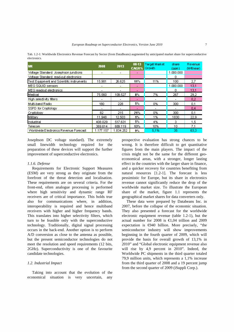
Tab. 1.2-1: Worldwide Electronics Revenue Forecast by Sector (from DataBeans) augmented by anticipated market share for superconductive electronics.
Josephson DC voltage standard). The extremely small linewidth technology required for the preparation of these devices will support the further improvement of superconductive electronics.
1.1.6. Defense Requirements for Electronic Support Measures
(ESM) are very strong as they originate from the forefront of the threat detection and localisation. These requirements are on several criteria. For the front-end, often analogue processing is performed where high sensitivity and dynamic range RF receivers are of critical importance. This holds true also for communications where, in addition, interoperability is required and hence multiband receivers with higher and higher frequency bands. This translates into higher selectivity filters, which turn to be feasible only with the superconductive technology. Traditionally, digital signal processing occurs in the back-end. Another option is to perform A/D conversion as close to the antenna as possible, but the present semiconductor technologies do not meet the resolution and speed requirements (12 bits, 2GHz). Superconductivity is one of the favourite candidate technologies.
1.2. Industrial Impact
Taking into account that the evolution of the economical situation is very uncertain, any
prospective evaluation has strong chances to be wrong. It is therefore difficult to get quantitative figures from the main players. The impact of the crisis might not be the same for the different geo-economical areas, with a stronger, longer lasting effect in the countries with the larger share in finance, and a quicker recovery for countries benefiting from natural resources [1.2-1]. The forecast is less pessimistic for Europe, but its share in electronics revenue cannot significantly reduce the drop of the worldwide market size. To illustrate the European share of the market, figure 1.1 represents the geographical market shares for data converters only.
These data were prepared by Databeans Inc. in 2007, before the collapse of the economic situation. They also presented a forecast for the worldwide electronic equipment revenue (table 1.2-1), but the actual number for 2008 is €1,04 trillion and 2009 expectation is €940 billion. More precisely, “the semiconductor industry will show improvements beginning in the fourth quarter of 2009, which will provide the basis for overall growth of 13,1% in 2010” and “Global electronic equipment revenue also will rise by 4,9 percent in 2010”. Indeed, the Worldwide PC shipments in the third quarter totaled 79,9 million units, which represents a 1,1% increase from the third quarter of 2008 and a 19 percent jump from the second quarter of 2009 (iSuppli Corp.).

1. Social and economic impact of superconductive electronics 8
Fig. 1-1: 2008 worldwide data converter revenue share by region (Databeans 2007).
However, if we disregard the effect of the crisis,
we can use the worldwide industrial electronics revenue forecast in 2013 from Databeans Inc. to estimate the market share for superconductive electronics. This is presented table 1.2-1 with a resulting market size estimate in the 50M€/year range. ISTEC is estimating an annual revenue for superconductivity (including the Energy, Medical and Transport domains) of more than $3 billion. The average growth over 2008-2013 for market segments of interest for superconductive electronics is about 5%, which is less than the overall market growth rate (9%). However, the SIPRI group quotes [1.2-4] that the worldwide expenditure for arms has been increasing at an average (1998-2007) yearly rate of almost 4%. With the new profile of the world leaders, we may suspect that the growth rate for electronics in the military domain will be larger than the Databeans forecast of 1%. These estimates would apply to packaged components, but do not include the market share for cryocoolers. Although the amount is not very appealing, some of the products such as the voltage standard are only feasible in this technology, which cannot be dropped altogether.
With all the applications listed above, what will be the industrial infrastructure required to meet the potential market ?
The applications reviewed in 1.1 will probably open the market for several technologies: we try here to estimate what will be the share of each technology, i.e. the volume of circuits to be produced for each technology.
The presently most mature technology, i.e. the Nb/Al, has been used to produce a wide variety of
demonstrators and can be used for virtually all the superconducting circuits (although in some specific cases, other technologies are preferred). But the 4K cooling requirement is presently limiting the appli-cation field, for either financial or technical grounds. The development of the application field essentially depends on the operational advantage over non-superconductive technologies, i.e. partly due to the functionality of the circuit, partly due to the cryo-cooler performance at the temperature of operation.
The functionality of a superconducting circuit might be increased by increasing its complexity. As this development is foreseen for the mature Nb/Al technology, it will increase the number of superconducting circuits in future systems. A few industrial foundries are already existing for Nb/Al circuits (Cf. §4.1), but there are reasons why other Nb/Al foundries might be necessary : strategic (specialised applications), political (European competitiveness), technological (backup source), etc.
The cryocooler performance is gradually improving, but there is little hope that a breakthrough will radically change the potential application domain for a given temperature of operation (equivalently to a given superconducting technology). Refer to the discussion §5.1 for more details.
Other technologies are being developed for specific applications, either where a lower tempe-rature is required (e.g. quantum computation), or for higher temperature of operation when cooling at 4 K is not mandatory or not acceptable (onboard applications). Higher Tc superconducting materials, such as NbN, MgBB2 and/or YBCO (cf. §4.2, 4.3, 4.4), can be used to reduce the cooling power and operation cost. However, this holds only for the moderate to low complexity circuits for technology maturity reasons (cf. 3.2.1).
In the “Superconducting Technology Assessment” for High End Computing [1.2-3] in 2005, the NSA concluded that there were no significant outstanding research issues for RSFQ technologies, that reliable projections could be made and that risks have been identified (e.g. memories). But the development of RSFQ technologies based on Niobium would require a comprehensive and sustained government funded program of approximately $100M/yr, as the private sector alone would not support the development and industrialization. Once the technology is developed,

European Roadmap on Superconductor Electronics, Version June 2010 9
These different technologies required for the range of applications, involving specific – or at least dedicated equipment – will probably be produced in different foundries. The concentration of a single technology at a single place, while this may be economically optimal from a supplier point of view, might be desirable only for the secondary technologies. It is not recommended to confine the mature process in a single foundry. This is risky for the customer in particular because there is no competition, also for technical reasons: it is safer to have a secondary source; and finally, political reasons may prevent access to the products (e.g. ITAR classified products). In Europe, small companies have spun-off from publicly-funded research targeting the market with SQUID-based small systems: this illustrates the difficulty encountered with super-conductors: components need expertise in cryogenics in addition to special expertise in packaging to insert them in a system. The level of expertise required for superconducting devices is higher than for semi-conductor electronics; it is safer to design the whole system in a collaborative way than to just handle products from supplier to customer as is the case in semiconductor industry.
it will find applications for other governmental bodies, and may eventually develop commercial applications as well.
The European Nanoelectronics Advisory Council (ENIAC) claims that intelligent systems combining ‘More Moore’ (higher speed for digital circuits) and ‘More than Moore’ (diverse analog functions) are required. They come to the conclusion that high speed data converters are crucial. This will increase the demand for superconductive ADCs in professional electronics, or quoting ITRS 2005, in “several important specific applications that are beyond the scope of ITRS". The more recent comment of ITRS (2007) on "Emerging Research Devices" is clearly restricted to Low-Tc super-conductivity: "RSFQ devices, systems and circuits have been developed, prototyped, and fabricated. They could become an important technology if the correct market driver emerges. Design and fabrication lines for RSFQ systems exist. Cryogenic operation, cost and material integration issues limit application space". It is true that neither LTS and HTS will ever penetrate the consumer electronics market, but the important specific applications (identified table 1.2-1) justify the research and development effort also proposed by NSA. Moreover, other technologies will also benefit from these developments, e.g. in data signal transmission (mainly optoelectronics).
For the simpler devices, such as passive microwave components, material can be grown in one place, while device is processed in another. This is usually done for HTS thin films and hetero-structures, fabricated on order within Europe. In this case, the need for another source is not clear: on one hand, the market is presently too small, and on another hand, material quality is more critical with Copper oxide perovskytes than with metals such as Nb. HTS device processing unit might exist in Eastern Asia for electronic devices and in Europe but probably only for power applications.
Another application domain is telecom-munications either onboard satellites or earth-based stations. While the requirement for earth-based stations might be comparable to those for High End Computing (cf. above), the situation is very different for satellites. Here, a 4 K cryocooler is not acceptable and technologies with a higher operating temperature might be preferred. The gain for a 128-channel receiver/transmitter operating at 9 K over its equivalent using standard technologies may not be sufficient to justify the choice of superconducting technology. The scaling is also important for ground-based communications, as when 100 Tbits/s router become necessary, the power dissipation with semiconductor technology is estimated to be larger than 300kW, where RSFQ circuits together with cryocooler dissipation will be about 10 kW [1.2-5].
For detectors and RSFQ circuits, FLUXONICS, a European initiative is presently responding to the demand for research and development: it is a distributed foundry with essentially academic partners involved in LTS, MTS and HTS circuit design and fabrication. But it is not structured/meant for volume production when this is required. Already existing SMEs might be able to grow with the demand of these products within their area of expertise (e.g. SQUIDs). In the coming years, other fields such as encrypted communications might
Structure of industrial network:
1. Social and economic impact of superconductive electronics 10
develop, with a demand of single photon super-conducting detectors for which nearly only one supplier exists.
Superconductor electronics are used by telecom operators (microwave filters), calibration laboratories (voltage standard) and for magnetometry (medical, geomagnetism…). Research infrastructures have long been using superconductor electronics also as detectors, mixers, photon counters… Most appli-cations of superconducting electronics correspond to a specialised market: as for any physics R&D domain, it requests specialised suppliers with a very good knowledge of the physics involved, accepting some innovation rate [1.2-2]. Supplier and customer have mostly R&D partners relationship which help to maintain the necessary industrial and technical expertise in a fluctuating market. The innovation generated may open new markets. As the technology matures, more regular customer/supplier relationship will develop. Additionally, market fluctuation will smoothen. Another impact stems from the fact that the high level of technicity developed in industry gives a positive image to address other markets.
Reference
1.2-1]“Global Europe Anticipation Bulletin” n°30, from LEAP/Europe2020 (http://www.leap2020.eu)
[1.2-2] ERID-Watch Conference, Prague, Oct. 2008. [1.2-3] “Superconducting Technology Assessment” NSA 2005,
http://stinet.dtic.mil/cgibin/GetTRDoc?AD=ADA464659 [1.2-4] SIPRI YEARBOOK 2008, SUMMARY: http://www.
sipri.org/contents/milap/milex/mex_database1.html [1.2-5] M.Hidaka, Superconductivity Web21, Winter 2009.
European Roadmap on Superconductor Electronics, Version June 2010
11
2. Basics of Superconductor Electronics
2.1. Superconductivity
By applying a voltage to a metal, the electrons drift as electrical current under the influence of the electric field. As the current flow reaches a steady state the electrons must meet a resistance to their passage through the metal. The resistance is caused by diverse mechanisms of inelastic electron scattering which leads to a linear temperature dependence of the resistance at higher temperatures. At room temperature the scattering process is generally dominated by quantized modes of lattice vibrations, the phonons and, at very low temperatures, electron-electron scattering and impurity scattering become relevant.
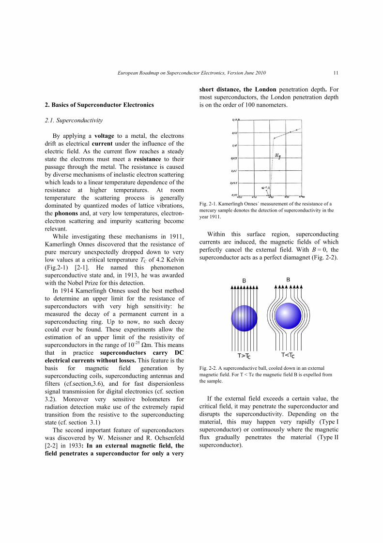
While investigating these mechanisms in 1911, Kamerlingh Onnes discovered that the resistance of pure mercury unexpectedly dropped down to very low values at a critical temperature TC of 4.2 Kelvin (Fig.2-1) [2-1]. He named this phenomenon superconductive state and, in 1913, he was awarded with the Nobel Prize for this detection.
In 1914 Kamerlingh Onnes used the best method to determine an upper limit for the resistance of superconductors with very high sensitivity: he measured the decay of a permanent current in a superconducting ring. Up to now, no such decay could ever be found. These experiments allow the estimation of an upper limit of the resistivity of superconductors in the range of 10-25 Ωm. This means that in practice superconductors carry DC electrical currents without losses. This feature is the basis for magnetic field generation by superconducting coils, superconducting antennas and filters (cf.section,3.6), and for fast dispersionless signal transmission for digital electronics (cf. section 3.2). Moreover very sensitive bolometers for radiation detection make use of the extremely rapid transition from the resistive to the superconducting state (cf. section 3.1)
The second important feature of superconductors was discovered by W. Meissner and R. Ochsenfeld [2-2] in 1933: In an external magnetic field, the field penetrates a superconductor for only a very
short distance, the London penetration depth. For most superconductors, the London penetration depth is on the order of 100 nanometers.
Fig. 2-1. Kamerlingh Onnes´ measurement of the resistance of a mercury sample denotes the detection of superconductivity in the year 1911.
Within this surface region, superconducting
currents are induced, the magnetic fields of which perfectly cancel the external field. With B = 0, the superconductor acts as a perfect diamagnet (Fig. 2-2).
Fig. 2-2. A superconductive ball, cooled down in an external magnetic field. For T < Tc the magnetic field B is expelled from the sample.
If the external field exceeds a certain value, the
critical field, it may penetrate the superconductor and disrupts the superconductivity. Depending on the material, this may happen very rapidly (Type I superconductor) or continuously where the magnetic flux gradually penetrates the material (Type II superconductor).
2. Basics of Superconductor Electronics 12
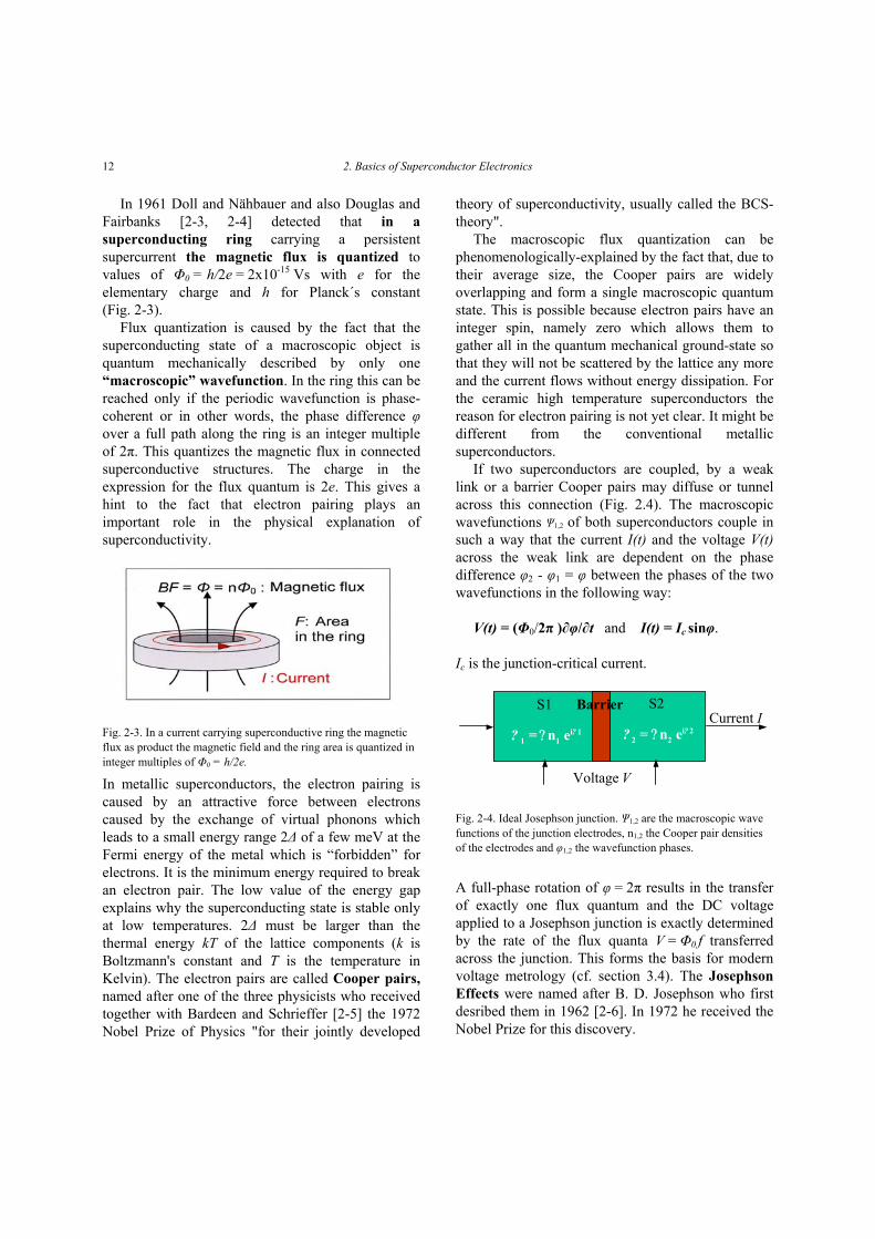
In 1961 Doll and Nähbauer and also Douglas and Fairbanks [2-3, 2-4] detected that in a superconducting ring carrying a persistent supercurrent the magnetic flux is quantized to values of Φ0 = h/2e = 2x10-15 Vs with e for the elementary charge and h for Planck´s constant (Fig. 2-3).
Flux quantization is caused by the fact that the superconducting state of a macroscopic object is quantum mechanically described by only one “macroscopic” wavefunction. In the ring this can be reached only if the periodic wavefunction is phase-coherent or in other words, the phase difference φ over a full path along the ring is an integer multiple of 2π. This quantizes the magnetic flux in connected superconductive structures. The charge in the expression for the flux quantum is 2e. This gives a hint to the fact that electron pairing plays an important role in the physical explanation of superconductivity.
Fig. 2-3. In a current carrying superconductive ring the magnetic flux as product the magnetic field and the ring area is quantized in integer multiples of Φ0 = h/2e.
In metallic superconductors, the electron pairing is caused by an attractive force between electrons caused by the exchange of virtual phonons which leads to a small energy range 2Δ of a few meV at the Fermi energy of the metal which is “forbidden” for electrons. It is the minimum energy required to break an electron pair. The low value of the energy gap explains why the superconducting state is stable only at low temperatures. 2Δ must be larger than the thermal energy kT of the lattice components (k is Boltzmann's constant and T is the temperature in Kelvin). The electron pairs are called Cooper pairs, named after one of the three physicists who received together with Bardeen and Schrieffer [2-5] the 1972 Nobel Prize of Physics "for their jointly developed
theory of superconductivity, usually called the BCS-theory".
The macroscopic flux quantization can be phenomenologically-explained by the fact that, due to their average size, the Cooper pairs are widely overlapping and form a single macroscopic quantum state. This is possible because electron pairs have an integer spin, namely zero which allows them to gather all in the quantum mechanical ground-state so that they will not be scattered by the lattice any more and the current flows without energy dissipation. For the ceramic high temperature superconductors the reason for electron pairing is not yet clear. It might be different from the conventional metallic superconductors.
If two superconductors are coupled, by a weak link or a barrier Cooper pairs may diffuse or tunnel across this connection (Fig. 2.4). The macroscopic wavefunctions Ψ1,2 of both superconductors couple in such a way that the current I(t) and the voltage V(t) across the weak link are dependent on the phase difference φ2 - φ1 = φ between the phases of the two wavefunctions in the following way:
V(t) = (Φ0/2π )∂φ/∂t and I(t) = Ic sinφ.
Ic is the junction-critical current.
Fig. 2-4. Ideal Josephson junction. Ψ1,2 are the macroscopic wave functions of the junction electrodes, n1,2 the Cooper pair densities of the electrodes and φ1,2 the wavefunction phases.
A full-phase rotation of φ = 2π results in the transfer of exactly one flux quantum and the DC voltage applied to a Josephson junction is exactly determined by the rate of the flux quanta V = Φ0 f transferred across the junction. This forms the basis for modern voltage metrology (cf. section 3.4). The Josephson Effects were named after B. D. Josephson who first desribed them in 1962 [2-6]. In 1972 he received the Nobel Prize for this discovery.
S1 S2
? 1 = ?n1 ei? 1 ? 2 = ?n2 ei? 2
BarrierCurrent I
Voltage V

European Roadmap on Superconductor Electronics, Version June 2010
13
By combining one or two Josephson junctions and a superconducting ring, extremly sensitive magnetic field detectors, Superconducting Quantum Interference Devices or SQUIDs can be established. The junctions allow to enter flux quanta to the ring in a controlled manner. (for more details cf. section 3.3 and [2-7] and for a general introduction cf. [2-8, 2-9]).
An introduction to superconductivity and more details can be found in many textbooks, e.g. [2-10, 2-11].
2.2. Superconductive Materials
Conventional superconductors, such as pure metals and metal alloys, exhibit superconductivity at temperatures up to about 23 K. The most widely used superconductor, niobium, for example, has a critical temperature of 9.26 K. Their behaviour is well understood with the BCS theory. These materials are named in general low-temperature superconductors (LTS).
The highest critical temperature found for a conventional superconductor is 39 K for magnesium diboride (MgB2) discovered in 2001. This material has been identified as two-band superconductor in which each band behaves like a conventional BCS-superconductor.
High-temperature superconductors (high-Tc or HTS) are materials that have superconducting transition temperatures above 30 K. The first superconductor of this type was discovered in 1986 by K. Müller and J. Bednorz [2-12], for which they were awarded the Nobel Prize in Physics in 1987. These HTS materials (often referred to as cuprates) are quasi-two-dimensional materials with their superconducting properties characterized by electron or hole pairs moving within weakly coupled copper-oxide (CuO2) layers. Neighbouring layers contain ions like La, Ba, Sr, or other atoms. They stabilize the structure and dope electrons or holes onto the copper-oxide layers. Cuprate superconductors have high critical temperatures compared with LTS: YBa2Cu3O7, one of the first cuprate superconductors to be discovered, has a critical temperature of 92 K. The best known high-temperature superconductors are bismuth strontium calcium copper oxide, BSCCO and yttrium barium copper oxide, YBCO.
The highest superconducting transition temperature (Tc) so far obtained is for a material where the charge reservoir consists of mercury oxide; here Tc is with more than 130 K, 50 % higher than in YBCO.
Recently a number of superconductors with HTS were found which are not based on copper oxide layers. The most recent type is a iron–arsenide superconductor discovered in 2008 which shows a Tc of about 55 K and better isotropic current carrying characteristics than the cooper oxide superconductors. These materials are currently being investigated for electronics and power applications.
Two decades of intense experimental and theoretical research, have highlighted many common features in the properties of high-temperature superconductors, but as of 2009 there is no generally-accepted theory to explain their properties.
As ceramics are not ductile like metals it is rather difficult to form wires and electronic components like Josephson junctions with high reproducibility and reliability. While for the wire fabrication acceptable solutions have been found, the manufacture of integrated HTS electronic circuits is still restricted to a low number of junctions. Complex electronic compounds with more than 100 circuit elements are exclusively made of conventional superconductors like Nb or NbN.
Most of the physical properties of superconductors vary from material to material, such as the heat capacity and the critical temperature at which superconductivity is destroyed. Superconductivity does not occur in noble metals like gold and silver, nor in ferromagnetic metals such as iron. An overview on material properties of superconductors can be found e.g. [2-13, 2-14].
2.3. Power Application and Challenges
Today, high field magnets are the main application for conventional superconductors. At a given field, superconducting magnets are much smaller than their conventional counterpart, because the windings can carry large currents with no energy loss. Superconducting magnets are already crucial components of several technologies. Magnetic resonance imaging (MRI) is fully established in diagnostic medicine and plays an even increasing role. They are used for NMR systems, mass

2. Basics of Superconductor Electronics 14
spectrometers, and magnetic separation, where weakly magnetic particles are extracted from a background of non-magnetic particles. The intense constant magnetic fields which are needed for these instruments are a perfect application for superconductors. Particle accelerators like the LHC in CERN require high-field superconducting magnets for the control of the particle beam. In the same sector only superconductive resonators have a sufficiently high quality factor for the generation of the accelerating microwave fields. The ITER project for power generation with nuclear fusion would be unthinkable without the huge toroidal magnet that captures the ultra-hot high-pressure plasma which is to ignite the fusion .
Most of the large scale applications are not realized because of saving energy but because superconductivity is the only way to reach the objectives. Superconductivity is of fundamental importance in research.
At present most of the large scale applications employ the well-understood conventional superconductors. But it is expected that high-temperature superconductors will soon become more cost-effective in many cases due to the possibility of liquid nitrogen cooling. Both the US and Japan have plans to replace underground copper power cables with superconducting BSCCO cable-in-conduit cooled with liquid nitrogen. By doing this, more current can be routed through existing cable tunnels. In one instance 250 pounds of superconducting wire replaced 18,000 pounds of vintage copper wire, making it over 7000 % more space-efficient. Promising future applications include high-performance transformers, power storage devices, electric power transmission, electric motors (e.g. for vehicle propulsion, as in vactrains or maglev trains), magnetic levitation devices, and fault current limiters. Recently, power utilities have begun to use superconductor-based transformers and fault current limiters . The use of superconductors for transportation has already been established using liquid helium as a refrigerant. Also liquid nitrogen cooled high-TC magnets for levitation are currently investigated. In Japan prototype levitated trains have been constructed and tested which are planned to connect Tokyo and Osaka with a high speed connection within a few years
However in contrast to DC currents, alternating currents are not completely lossless in superconductive wires, so that AC applications like transformers will be more difficult to develop than those instruments that rely upon DC. AC losses can be minimized by splitting the wires into a large number of tiny filaments. It is real challenge to transfer this fabrication process from the well understood NbTi-process to HTS brittle ceramic materials. At present it is not possible to fabricate 100 km long high quality wires which are needed for the generation of very high fields.
Markets will arise where the relative efficiency, size and weight advantages of devices based on HTS outweigh the additional costs involved.
2.4. Electronics Application and Challenges
Superconductive Electronics are planar integrated circuits consisting of passive circuit elements like superconductive wiring, resistors, inductors, capacitors and active components like Josephson junctions and SQUIDs. The technology applied for realizing superconductive circuitry depends on the degree of complexity. At present, practically all applied circuits of high complexity are made of Nb or NbN. An introduction to the physics of superconductive electronics is given in [2-15]
In the simplest case suitably patterned superconductive thin films are as used highly efficient microwave antennas or filters for mobile communication. Nanometre-sized thin film structures are serving as ultra-sensitive particle or single photon detectors. Superconductive detectors cover the whole frequency range from radio waves to X-rays. Transition edge sensors (TES) where the radiation to be detected drives a small superconductor, biased close to the transition point, to the normal state, reach a noise equivalent power of 5×10-20 W/√Hz. The Atacama Cosmology Telescope features in its millimetre bolometer array camera one of the largest TES array sets currently in production or in use. With three arrays of 1,024 pixels each, it has only recently been operated in its complete configuration. Another important field of TES is THz imaging for security applications. A detailed overview of different detectors and multiple application fields is given in Section 3.1.

European Roadmap on Superconductor Electronics, Version June 2010
15
The next level of complexity is reached by integrating one or two Josephson junctions in a superconducting ring. The superconducting ring can pick-up external magnetic fields inducing a circulating current inside the ring. The voltage amplitude of the interference pattern depends on this current and can be used to measure weak magnetic fields or currents. This topology is called Superconducting Quantum Interference Device SQUID. SQUIDs permit the detection of magnetic fields as small as 1 fT/√Hz. SQUID magnetometers are used worldwide to measure magnetic signals from the heart, brain, and other organs. They have proven their excellent features in non-destructive material evaluation like crack detection in aircraft wheels. An airborne full-tensor magnetic gradiometer SQUID using liquid-helium-based thin-film technology together with system electronics, data acquisition system, and cryogenics has been developed and extensively tested. Successful field investigations
were conducted by towing the system from a helicopter as well as for a stinger-mounted configuration in a Cessna 208 aircraft. While a SQUID clearly is an accepted and productive research instrument, the application of this technology in routine clinical diagnosis is only now beginning. The majority of the effort in the field has been by university and national-laboratory researchers and by small, high-technology companies, and has been directed towards the development and promotion of this technology. Fig. 2-5 shows the advanced status of the circuit technology.
The introduction of HTS materials has led to enormous efforts to transfer the experiences with LTS devices into a technology based on HTS and by this make use of the much easier cooling. This was successful for passive devices like microwave filters and antennas in mobile phone base stations which are commercially available and in practical use in the USA. Similar trends are evident in the use of SQUIDs for the non-destructive evaluation (NDE) of aircraft parts and other materials: most of the effort is directed towards instrumentation development and demonstrations in simple systems. HTS SQUIDs can achieve a white noise level as low as 10 fT/√Hz at 77 K, which only marginally exceeds the noise of commercial niobium-based SQUIDs operating at 4.2 K. Section 3.3 provides an overview of possible applications for extremely sensitive analogue sensors based on SQUIDs.
The highest level of complexity is required for digital circuits, where signal propagation and logic operation is based on the dynamic manipulation of single flux quanta. For digital signal processing, highly integrated multi-level circuits are required which combine Josephson junctions, SQUIDs, resistors, inductors and superconductive wiring to Rapid Single Flux Quantum (RSFQ) electronics [2-16]. Discrete switching between the states is performed by pulses of the Josephson junctions. The suitable parameters given, a SQUID provides two stable flux states which denote flux “0” and flux”1”. As each pulse corresponds to the transfer of a single flux quantum, SE provides an intrinsic digitization on an exact quantum basis. The complete switching cycle takes about 5 picoseconds with a total energy consumption of about 10-18 Joule. The optimum operation frequency is determined by characteristic voltage, a product of the critical current and the normal state of the Josephson junction. A voltage of 1 millivolt corresponds to an oscillation frequency of about 500 GHz (cf. section 2.1). The outstanding advantage of RSFQ electronics is the extremely low power consumption at very high speed operation. A good example is a reconfigurable-data-path processor prototype with 23 GHz clock frequency and a total power consumption of only 4.1 mW [2-18]. In comparison to standard semiconductor state-of-the-art processors, this is an operation speed about 10 times faster at a power consumption about 10,000
Fig. 2-5: 4-inch silicon wafer with niobium SQUID sensors in magnetometer and gradiometer configuration (IPHT).

2. Basics of Superconductor Electronics 16
times less. For small circuits high speed operation up to 750 GHz was shown [2-19]. Fig. 2-6 shows a 2 x 3 reconfigurable-data-path processor with 14,040 Josephson junctions and designed for an operation speed of 23 GHz.
Fig. 2-6 Photograph of 6.8 x 6.7 mm2 2 x 3 reconfigurable-data-path processor with 14,040 Josephson junctions [2-17] with courtesy of A. Fujimaki.
The on-chip communication in superconducting
circuits provides an important advantage in comparison to all other existing integrated circuit technologies. Transient data pulses can be transferred on lossless interconnects with an ultimate delay of only 8 picoseconds per millimetre. No degradation caused by dispersion disturbs the on-chip communication at high-speed. An extensive assessment of RSFQ electronics, its potential and an estimate of the costs of development are given in [2-20]
The digital application mentioned as examples are demonstrators in the research community. Fully established in legal metrology and commercially available as DC and AC voltage standards are special Digital to Analogue Converters with up to 70000 junctions and more which make use of the Josephson junction feature to convert a flux quantum transfer rate into a DC voltage (cf. Section 2.1 and section 3.4) (Fig. 2-7). Transferring and counting the flux quanta by means of a precise frequency control can
be done with fundamental precision. Such devices can also be used as voltage controlled high frequency oscillators.
Fig. 2-7. 3 inch wafer with standard chips for AC and DC voltage standards (PTB).
Nearly all the described application fields require
complex circuitry or very small and thin structures. To further improve the circuit performance, a higher degree of integration at decreasing linewidths is required. At present this can be reached only with metallic superconductors like Nb and NbN. Cooling to 4.2 K is performed by liquid Helium or small cryocoolers. In many cases the low temperatures are required to reduce the thermal noise. This is the case for ultra-sensitive SQUIDs and detectors. To bring superconductive electronics to commercial applications adapted low-cost and reliable cooling systems must be developed. The required degree of integration can be reached only by implementing a stable infrastructure for circuit fabrication.
By preparing small digital HTS circuits it has been shown that all logic functions can be realized. A 125 GHz RSFQ sampler system for observing ultra-fast signals and a high temperature superconducting sigma-delta A/D converter with ramp edge junctions and an internal clock of up to 174 GHz has been successfully tested. The large energy gap of HTS opens the potential of reaching extremely high operation frequencies up to THz.

European Roadmap on Superconductor Electronics, Version June 2010
17
The main obstacle for manufacturing more complex HTS and MgB2 circuits is the lack of a junction and multi-layer circuit technology which allows the connection of more than a few hundred Josephson junctions. The junctions still have a parameter spread too large for high speed RSFQ circuits.
Reference [2-21] gives a broad overview on the status of all applications fields.
References
[2-1] H. Kamerlingh Onnes, Akad. Van Wetenschappen (Amsterdam) 14, 113, 818, (1911)
[2-2] W. Meißner, R. Ochsenfeld, Naturwiss. 21, 787 (1933) [2-3] R. Doll, M. Näbauer, Phys. Rev. Lett. 7, 51 (1961) [2-4] B.S. Deaver Jr., W.M. Fairbank, Phys. Rev. Lett. 7, 43
(1961) [2-5] J. Bardeen, L.N. Cooper, J.R. Schrieffer, Phys. Rev. 108,
1175 (1957) [2-6] B.D. Josephson, “Possible new effects in superconductive
tunneling” Phys. Rev. Lett. 1, 251 (1962) [2-7] J. Clarke, A.I. Braginsky (eds.), “ The SQUID Handbook”
Wiley-VCH, Weinheim, 2006 ISBN-13: 978-3-527-40408-7, ISBN-10: 3-527-40408-2
[2-8] A.Barone, G. Paternó, Physics and Applications of the Josephson Effect, John Wiley & Sons, 1982, ISBN 0-471-01469-9
[2-9] K.K. Likharev, Dynamics of Josephson junctions and circuits, Gordon and Breach Publ., New York 1986
[2-10] Tinkham, Michael (2004). Introduction to Superconductivity (2nd ed. ed.). Dover Books on Physics. ISBN 0-486-43503-2 (Paperback).
[2-11] W. Buckel, R. Kleiner, “Superconductivity”, Wiley-VCH, Berlin , 2004, ISBN-13: 978-3-527-40349-3
[2-12] J.G. Bednorz and K.A. Mueller, "Possible high TC superconductivity in the Ba-La-Cu-O system". Z. Phys. B64 (2), 189–193 (1986)
[2-13] J. Evett, “Concise Encyclopedia of Magnetic and Superconducting Materials”, Elsevier publishers, 1992, ISBN: 9780080347226, ISBN-10: 0080347223
[2-14] Frontiers in Superconducting MaterialsNarlikar, Anant V. (Ed.) 2005, XXXII, 1104 p., Hardcover ISBN: 978-3-540-24513-1
[2-15] T. Van Duzer, C.W. Turner, Principes of Superconductive Devices and Circuits, 2nd Edition, Year of Publication: 1998, ISBN:0-13-262742-6 Prentice Hall PTR Upper Saddle River, NJ, USA
[2-16] K.K.Likharev, V.K.Semenov, “RSFQ logic/memory family”, IEEE Trans. Appl. Supercond. 1, 3-28 (1991)
[2-17] Fujimaki, A. and Tanaka, M. and Yamada, T. and Yamanashi, Y. and Park, H. and Yoshikawa, N., “Bit-Serial Signle Flux Quantum Microprocessor CORE”, IEICE Trans. Electron. Vol. E91-C, pp. 342-349, March 2008
[2-18] Will be published in ISEC 2009 as SP-O4: "Demonstration of 2x3 Reconfigurable-data-path Processors with 14000 Josephson Junctions", by Akira Fujimaki, Ryo Kasagi, Katsumi Takagi, Irina Kataeva, Hiroyuki Akaike, Masamitsu Tanaka, Naofumi Takagi, Nobuyuki Yoshikawa, and Kazuaki Murakami.
[2-19] T. Van Duzer, C. W. Turner, “Principles of superconductive devices and circuits”. New York, Elsevier, 1981. 369 p. QC612.S8V36
[2-20] http://www.nitrd.gov/pubs/nsa/sta.pdf [2-21] “Applications of Superconductivity” Proceedings of the
IEEE, Vol. 92, no. 10, October 2004
3. Application of Superconductor Electronics, Radiation Detectors 18
3. Application of Superconductor Electronics
3.1. Radiation Detectors
Superconducting photon and particle detectors are operated at temperatures close to absolute zero are being developed because of the extremely high performance that low temperature operation enables. The very low thermal budget for cooling puts strong limitations in detector size, number and count rates.
Research on ultra-low temperature photon detectors has traditionally been driven by the need for high energy resolution in X-ray astronomy and fundamental physics. This work has produced a good understanding of most of the basic detector science. Current research focuses on building detector arrays to increase area, count rate and imaging capabilities. More recently, applications have been extended to biophysics, quantum optics and material science. This research is more diverse and thus less coordinated. It is now desirable to expand the use of cryogenic photon detectors beyond the astrophysics applications they were initially developed for, and adapt their use for broader scientific and societal needs.
This document describes the current status of superconducting detector research, and suggest areas for future development.
3.1.1. Superconducting Detector Technologies A common way to detect electromagnetic
radiation is to absorb incoming photons to an appropriate absorber, where its energy causes a temperature rise. Usually it is differentiated whether the detector can discriminate single events, giving the opportunity to derive the energy of the impacting photon (“calorimeter mode” or “Geiger mode”), or if a constant flux of many photons sum up, resulting in a measure of the power (“bolometer mode”).
Transition-Edge Bolometer (TES) In a bolometer, equilibrium between incoming
radiation power and cooling by a weak thermal link arises at a temperature above the cold bath.
Fluctuation in the thermal transport with the thermal conductance G limits the power sensitivity.
Superconducting detector technology in both cases relies on the use of a superconductor operated close its transition point to measure the temperature signal. This implies two consequences: Firstly, one needs a superconducting material with a transition point at the chosen working temperature, and secondly, this operating temperature has to be extremely stable. In practice, due to the sharp increase of detector resistance and dissipation during detection, this would make the concept almost unfeasible.
TES microcalorimeters use a bilayer of normal metal and superconductor films whose thicknesses are small compared with the coherence length in the metal, producing a proximity effect that lowers the superconducting transition temperature and normal state resistance of the bilayer [3.1-2]. One can reliably choose a convenient transition temperature by varying the relative thickness of the two films. Because this superconducting transition is narrow (<1 mK), these films are very sensitive thermometers. Their sensitivity can be up to two orders of magnitude higher than that of other thermometer technologies [3.1-3].
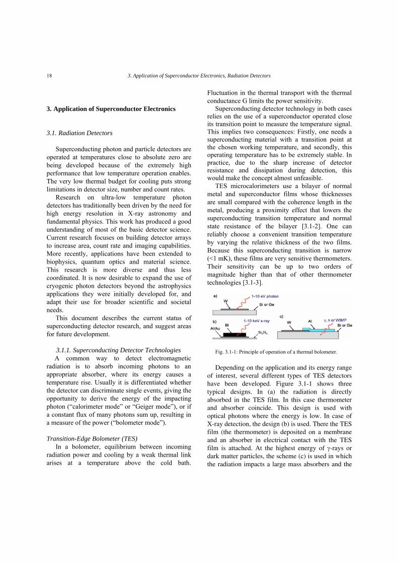
Fig. 3.1-1: Principle of operation of a thermal bolometer. Depending on the application and its energy range
of interest, several different types of TES detectors have been developed. Figure 3.1-1 shows three typical designs. In (a) the radiation is directly absorbed in the TES film. In this case thermometer and absorber coincide. This design is used with optical photons where the energy is low. In case of X-ray detection, the design (b) is used. There the TES film (the thermometer) is deposited on a membrane and an absorber in electrical contact with the TES film is attached. At the highest energy of γ-rays or dark matter particles, the scheme (c) is used in which the radiation impacts a large mass absorbers and the

European Roadmap on Superconductor Electronics, Version June 2010 19
resulting high frequency phonons generate quasiparticles in a superconducting film which diffuse to the TES film.
Because the TES has low impedance, it couples well to SQUID (Superconducting Quantum Interference Device) amplifiers and has low susceptibility to micro-phonics. SQUIDS also have the advantage of naturally operating at low temperatures and having extremely low (-nW) power requirements.
Detectors are read-out by applying a voltage bias across the TES and measuring the current through the sensor with a SQUID [Fig. 3.1-2]. Voltage biasing has the advantage of a phenomenon known as “negative electro-thermal feedback.” The resistance of a TES drops as it is cooled through its transition, leading to an increase in the V2/R Joule heating of the film. This heating leads to a stable equilibrium temperature, depending upon the voltage applied and the thermal conductivity of the link between the TES and its heat bath. If the bath temperature is significantly lower than this equilibrium temperature, the equilibrium becomes independent of the bath temperature. In addition, response times in the TES are shortened by the electro-thermal feedback: when a TES is heated by an incident photon radiation, its resistance increases, leading to lower Joule heating and thus to a more rapid return to equilibrium temperature. The resulting pulses are up to two orders of magnitude shorter than the natural time constant of the device [3.1-1]. TES is the detector of choice when energy resolution is the requested factor-of-merit and moderate detector speed can be tolerated. Since both the energy resolution and sensitivity improve at very low temperature, TES is operated in the millikelvin region.
Superconducting Nanowire Single-Photon Detector (SSPD)
Thermal bolometers and calorimeters, as described in the paragraphs above, rely on the conversion of the absorbed energy to lattice vibrations. This process is relatively slow and restricts the time constant of such detectors to be of order of µs and slower.
This speed limitation can be circumvented in case of a very small absorber volume. In that case, excited electrons which are created in the hot spot of photon impact can be read out before they relax to the lattice.
Fig.3.1- 2: 288-pixel TES Array with SQUID multiplexer applied to the project LABOCA [3.1-3].
The ability to discriminate the impact of single
photons obviously depends on the wavelength of the photon, i.e. its energy. The crossover from bolometer to calorimeter mode for low TC superconducting detectors typically can be found at short infrared wavelengths. For higher energy photons (visible, UV), most of the used detector types can work as single-photon detectors for specific wavelengths.
One particular concept is tailored to the detection of single photons only. In literature it is referred to as superconducting (Nanowire) single-photon detectors or SSPD.
Basically an SSPD consists of a very thin superconducting film (thickness about 6 nm), which is patterned into a narrow strip typically below 0.5 µm wide. The operation regime in the absence of an external magnetic field is to bias the device by a direct current that has a value very close to the critical current value. An impacting photon which is absorbed in the film will create a hotspot, where the superconducting state is locally destroyed. The
3. Application of Superconductor Electronics, Radiation Detectors 20
consequence is a short voltage pulse, which disappears whilst the narrow strip cools back to superconductivity and as the bias current inductively reset.
Fig. 3.1-3 A 10 µm diameter, 0.1 µm line-width spiral NbN Nanowire SSPD and its centre detail, patterned on 4-inch sapphire [3.1-5]
The development of such detectors requires ultra-
thin superconducting films that would allow one to reach the ultimate response-speed of these devices. Niobium nitride film with thickness of 4 nm and superconducting transition temperature TC ≈ 10 K after processing is the most popular material for SSPD applications in the 2 K-4 K operating temperature range with extremely low noise (NEP~10-20 W Hz-1/2). This sets the liquid-helium operation temperature of modern detectors, e.g. superconducting single-photon detector (SSPD) and hot-electron bolometer (HEB) mixer close to 0.5 TC. In numerous electronic applications of superconductivity, a combination of narrow strips made from thin superconducting films is the most frequently used device layout. A typical operation regime, e.g. for superconducting radiation sensors
working in the absence of an external magnetic field, is when the device is biased by a direct current that often has a value very close to the critical current value. The development of ultra-sensitive superconductive detectors and mixers, whose response is based on radiation induced heating of electrons, requires ultra-thin superconducting films that would allow one to reach the ultimate response-speed of these devices. However, the detection mechanism in these devices and subsequently the requirements for the superconducting structures differ significantly.
A comparison of superconducting and semi-conducting single-photon detectors is given in Table 3.1-1.
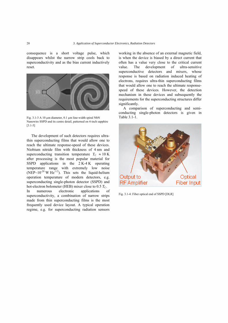
Fig. 3.1-4: Fiber optical end of SSPD [DLR]
European Roadmap on Superconductor Electronics, Version June 2010 21
Tab. 3.1-1: Comparison of photon counting SSPD and semiconducting APD [3.1-6]
Semiconducting APD Superconducting SPD
Detectors Si InGaAs SSPD TES
Temperature (K) 300 200 2 – 4.2 0.1
Wavelength (µm) 0.4 – 1.1 0.9 – 1.7 0.4 – 5.6 0.1 - 5
Time resolution 300 ps 300 ps 18 ps 300 ns
Quantum efficiency 70% @ 630 nm 25% @ 1.55 µm >10% @ 1.55 µm >92% @ 1.55 µm
Dark-count rate (Hz) < 100 < 104 < 0.1 < 0.001
Maximum count rate 10 MHz 4 MHz 250 MHz 20 kHz
Photon number resolution Very limited No Yes (limited) Yes
Superconducting-Tunnel Junctions Superconducting tunnel junctions (STJs) consist
of two superconducting films separated by a thin insulating tunnel barrier and often include a quasiparticle trapping layer. Photon absorption creates free charge carriers by breaking up Cooper pairs and the magnitude of the subsequent temporary increase in tunnelling current can be measured to determine the photon energy Ex. The small superconducting energy gap Δ in the order of meV allows high energy resolution, and short excess charge life times of order µs allow comparably high count rates. Fluctuations in the charge generation and tunnelling processes limit the energy resolution of STJs.
Superconductor-Insulator-Superconductor (SIS) quantum mixers provide an approach to millimeter wave mixing - potentially offering conversion gain, a low local oscillator power demand, and potential mixer noise temperatures near the quantum limit [3.1-7]. The hope of using Niobium Nitride with a higher gap energy for achieving the same performance as the Niobium junctions, even above 1 THz, has not been fulfilled due to the difficulties of working with the NbN material. Initial experiments with Niobium-Titanium-Nitride, however, are strong indicators that this material will allow noise 4 hν/k temperatures as low as to be achieved even at frequencies as high as 900 GHz and beyond [3.1-8].
Niobium SIS devices for routine use in millimeter and submillimeter-receivers are currently fabricated at a few dedicated laboratories, including several
European laboratories, among them IRAM, SRON, KOSMA and (in the near future) OSO. Worldwide, they are very competitive.
It is hard to conceive how this very specialized fabrication can be transferred to industry in a cost-effective way. At least, the development work necessary to achieve the goals for the LSA/MMA mixers (SSB operation, wide IF bandwidth, sensitivity) can only be done in the laboratories. The current device fabrication techniques are low volume and are aimed at specialized production runs with widely varying designs.
Hot-Electron Bolometer Mixer Superconducting hot-electron bolometer (HEB)
mixers are becoming the heterodyne receiver of choice for high-sensitivity and high-spectrum-resolution (ν/Δν > 106) detection in astronomy and atmospheric studies 1.5 THz [3.1-9]. The noise performance of phonon-cooled superconducting NbN HEB mixers has approached ten times the quantum limit (10 hν/k) in the THz range. Another important parameter of superconducting HEB mixers is the intermediate frequency (IF) bandwidth, which needs to be sufficiently large for spectral observations since the continuous frequency tuning of THz local oscillator (LO) sources is very limited even impossible for optically pumped far infrared gas lasers. Phonon-cooled superconducting NbN HEB mixers on the silicon substrate have a gain bandwidth of about 3 GHz, which can be increased to approximately 5 GHz with an MgO buffer layer

3. Application of Superconductor Electronics, Radiation Detectors 22
introduced, satisfying the needs of astronomical and atmospheric observations [3.1-11].
Fig. 3.1-5.: THz-mixer block with Silicon lens [3.1-10].
Table 3.1-2: Evaluation summary of superconducting particle detectors
Technology Development status today
Low risk deve- lopment steps
General limits (for 1 pixel)
Open questions Expected impact
TES γ- and X-ray detectors
Small arrays; Prototypes in operation
European foun-dry desirable,
1 eV resolution at up to 10 keV; >1000 counts/s
Can array technology be scaled to >>1000 pixels? Is crosstalk in large arrays managable?
High-profile X-ray astronomy, Ground-based mm- and µ-wave telescopes, nuclear safeguards
STJ X-ray detectors
Small arrays; Prototypes in operation
Reliable STJ fabrication
5 eV resolution at up to 10 keV; >100.000 cts/s
Can STJs be built with high performance at several keV? Can low-noise ASICs be built?
Improved µ-analysis for semicon-ductors and nanotechnology;
SSPD Small arrays; Prototypes in operation
Reliable SSPD fabrication
0,1 Hz dark cts., 1 Gbit/s count rate
Can SSPDs be built with high Energy resolution, increase of Quantum efficiency
Improved optical tomography and microscopy analysis and spectroscopy, improved time resolution
SIS and HEB Single devices; Prototypes
Reliable SIS fabrication
SIS close to 5x quantum limit
Can HEB built with high performance for arrays?
Improved low noise receivers for radioastronomy and security applications
3.1.2. Important Applications
Gamma and X-Ray Detection Even un-cooled detectors for high energy photons
like gamma ray or x-ray usually can discriminate single events and in doing so create a statistics of the energy distribution of all incoming photons. In this sense they record a spectrum of the radiation of interest. Using superconducting detectors the spectral resolution is unprecedented. Most of the applications make use of this feature, which enables an identification of the material of the source.
Astrophysical science acts as precursor, so high budget projects like the proposed ESA cornerstone space mission XEUS accelerate the development of such detectors. On earth a variety of applications can benefit. TES has to compete with semiconductor micro-calorimeters. The development of TES micro-calorimeter arrays and their multiplexed readout is mostly driven by the need for extremely high energy resolution in X-ray astronomy. Characteristic X-rays indicate elemental abundance, and an energy resolution of 2 eV at 6 keV will resolve different ionic charge states and line broadening to infer temperature, density and velocity structure of supernova remnants, stellar coronae, intergalactic

European Roadmap on Superconductor Electronics, Version June 2010 23
plasmas and black holes. TES are also used as bolometers for cosmic-microwave back-ground
studies of cosmological inflation, dark energy and the evolution of the universe.
Lower energies, especially X-rays emitted by accelerated electrons in solid state contain a lot of spectroscopic information on the actual material. As an example, a superconducting calorimeter which detects the secondary X-ray radiation caused by the electron beam in a scanning electron microscope can enhance the microscopic image by material information allocated to the actual position in the image. TES have also been proposed for microanalysis of small defects on semiconductor wafers [3.1-12]. Defects below a few tens of nm are too small to be efficiently excited by high-energy electron microscopes, and require the use of low-energy electrons and thus soft X-rays for elemental analysis. TESs are then required to overcome line overlap, although their slow speed has so far keep them from widespread use in the semiconductor industry. Such an add-on x-ray spectrometer is commercially available for instance by Vericold Technology (Germany). The Polaris spectrometer is laid out as an inspection tool in fabs for semi conducting technology.
On the high end of the energy scale, the identification of radioactive material by recording its gamma or x-ray spectrum can clarify its origin, which is important for instance for security applications. Moreover, the high sensitivity of superconducting
detectors can help to trace such dangerous materials at border controls. Microcalorimeters are used in high-resolution Gamma (γ) [3.1-13, 14] and fast-neutron [3.1-15] spectrometers. TES γ-spectrometers can improve the precision of non-destructive isotope analysis of nuclear materials by an order of magnitude, which is important for nuclear safeguards and forensics [3.1-19].
Photon or particle absorption increases the absorber temperature, which is measured with the thermometer before both parts cool back down to the cryostat temperature through the weak thermal link. Thermal energy fluctuations across the weak link limit the energy resolution of calorimeters.
STJs are less appropriate for γ- or neutron spectrometry since they cannot be made large. Additionally they are inefficient for high-energy operation. Fig. 3.1-6 Analytic System Polaris [3.1-21].
The success of TES microcalorimeters has limited the need for superconducting tunnel junctions (STJs) in astronomy to optical wavelengths [3.1-17], where high count rate capabilities are more important than for X-rays. This has reduced the STJ fabrication facilities worldwide. Nevertheless, the higher speed has made STJ preferred in synchrotron research for chemical analysis of dilute samples by high-resolution soft X-ray analysis [3.1-18]. They have e.g. been used to study protein reaction mechnisms by X-ray spectroscopy on active metal sites, and to examine dopants in semiconductors. STJs could also overcome the count rate problem that TES detectors face for non-destructive analysis of small defects on semiconductor wafers [3.1-19].
STJs and calorimeters have been used to detect ion impacts and extend mass spectrometry to heavy molecules, although this work has slowed down recently. In the X-ray energy region (keV) a mention should be deserved to the detection of non photonic radiation, like heavy ions and molecules (fragment of DNA, proteins, polymers) [3.1-20]. The use of superconducting detectors for molecule mass spectrometry (STJ & SSPD) and X-ray fluorescence measurements (TES) on SEM for material elemental analysis are applications with potential for wide dissemination of superconductive sensors technology. For the application in ToF mass spectrometry, the energy range is in the X-ray (5-30 keV) region. Here four merit factors are important at mass values above

3. Application of Superconductor Electronics, Radiation Detectors 24
40 kiloamu, 1) efficiency, 2) time discrimination (<ns), 3) energy spectroscopy (100 eV), and 4) large area coverage (mm, cm). Two superconducting detectors are under R&D: first, STJ which fulfils all the requirements apart the
large area coverage, but at the cost of using millikelvin refrigerators; second, SSPD which at the moment does not have energy resolution and sufficient large area coverage.
Tab. 3.1-3: Comparison of standard and superconducting X-ray detectors [3.1-22].
Ultraviolet/Visible/Near infrared Spectral range The field of detection of ultraviolet, visible and
near-infrared light is covered by the established technologies of photoconductive detectors and CCDs. Superconducting detectors can do even better, however the need for this improvement is not yet well addressed.
Superconducting detectors have found some exclusive niches, where the ability to count single photons plays a substantial role, in combination with an extremely low false alarm rate (so called “dark counts”) and high speed. Quantum cryptography is the most prominent application example, where a secure transmission of confidential data is based on the transfer of a quantum key by single photons, which can not be intercepted without revealing the eavesdropper. For this application, SSPDs are best suited.
Detecting extremely small signals on a very short timescale (e.g. nanoseconds) becomes also important for analyzing biochemical processes by means of modern spectroscopic methods like Raman. The applications of such methods range from pharmaceutical industry to human medicine. Again
this would be the domain of SSPDs, which can be designed for different wavelengths ranging from ultraviolet down to near-infrared.
Requirements for new detectors are spectral-resolution and time-resolved detection capabilities, simultaneous measurements of fluores-cence photons, faster reading for time resolved imaging, improved quantum efficiency and shorten the time spread and large-pixels arrays.
Application drivers are diagnostics and testing of chemical and biological materials, long-distance optical communications (increasing the sensitivity would allow longer transmission links and release the need for amplification), and quantum cryptography at 1550 nm wavelengths. Optical quantum information processing (including IR and visible light) is at the frontier of modern physics and optics. Other applications are biomedical imaging techniques with ultrafast single-photon detection in the visible or near-IR, for example for time-correlated fluorescence spectroscopy and time-of-flight techniques such as optical tomography.
The fast time response of SSPD should allow access the dynamics of physical, chemical and biological processes with 10 ps temporal resolution

European Roadmap on Superconductor Electronics, Version June 2010 25
and single-photon sensitivity with an impact in the fields of nanotechnology, single-molecule spectroscopy and surveillance applications as well.
Far-infrared / Terahertz Detection Whereas, conventional photoconductors are
competitive for near-infrared and shorter wavelengths, the situation changes for longer waves. Already in infrared bands it becomes usual to cool the detector to decrease its thermal noise, and bolometers are amongst the most sensitive devices.
Fig. 3.1-7: System for Quantum cryptography [paper R Hadfield APL]. 3 K cooler from Symphonia project for Quantum cryptography.
For wavelengths longer than 10 µm,
superconducting detectors have their domain, up to the radio band of several millimeters, where electronic devices take over as best detectors. In the terahertz band, often defined between 0.1 and 10 THz, superconducting detectors are unsurpassed by any other existing technology.
Again, astrophysics enabled many of the current applications. Most of the sensor concepts described above have emerged due to demand for ultimate sensitivity needed for the research on the origins of our universe. Ambitious projects like the search for dark matter, or the measurement of the polarization of the cosmic microwave background advance the technology of superconducting detectors to new levels of complexity and sensitivity.
On earth, sensor technology is currently maturing from lab experiments to the first industrial applications. As an example, terahertz security cameras based on superconducting detectors are under development by a few groups, and they are on the cusp to be introduced to market. However, this constitutes only the very first implementation. The
whole expertise of ultra-sensitive detection even of spectral information can be applied to detect for instance explosives or drugs.
Fig. 3.1-8: THz Videocamera [3.1-3].
Alongside the security solutions, imaging applications at far-infrared or terahertz wavelengths will be boosted by the availability of array sensors. One can think of medical imaging, e.g. to trace skin cancer at early stages, enhanced night vision devices and so on. Similar to infrared imaging, the market will grow because of the ability to identify new applications, which are not yet obvious.
3.1.3. Conclusions for Detector Development Observing current trends it becomes obvious that
the main technology drivers are imaging applications, which require large arrays of sensors to fill the focal plane of an appropriate optics. Therefore a large effort has to be put on maturing single detectors to devices, which combine a large number of superconducting detectors and their readout whilst enhancing the manufacturing technology to make such focal plane array manageable and economically feasible. Due to the sophisticated sensors, this involves not only a pure chip design but the implementation of such devices into an adapted cryo environment, meaning a cryogen-free cooler and a low noise readout / data acquisition chain.

3. Application of Superconductor Electronics, Radiation Detectors 26
Table 3.1-4: Timeline for Radiation Detector Development
SE Radiation Detectors
Basic R&D
Basic R&D
Basic R&D
Basic R&D
Basic R&D
Basic R&D
Applied R&D
Applied R&D
Applied R&D
Applied R&D
Applied R&D
Applied R&D
First Appl.
First Appl.
First Appl.
First Appl.
First Appl.
First Appl.
Mature Appl.
Mature Appl.
Mature Appl.
Mature Appl.
Mature Appl.
Mature Appl.
2010 2011 2012 2013 2014 2015 2016 2017 2018 2019 2020
THz detectors and receivers
Medium SSPD Arrays
SSPD
Large TES Arrays
Small TES Arrays
TES
Besides, physics of detectors is not yet fully exploited. There is room for improvement regarding sensitivity, speed and response of all detector types. Especially fundamental research on quantum physics most certainly will advance the performance of superconducting sensors. In the first place such quantum limited detectors will be useful for scientific applications. Nevertheless, also future industrial applications will benefit from these advancements.
[3.1-7] G. Chattopadhyay et. al. 10th Intern. Conf. On Space THz Technology, March 16-18, 1999
[3.1-8] M.C. Gaidis et. Al., IEEE Trans. Microwave Theory Techn., Vol. MTT-44, 7, pp. 1130-1139, 1996
[3.1-9] H. Richter, A.D. Semenov, S. Pavlov, H.W. Hübers, L. Mahler, A. Tredicucci, H.E. Beere, D.A. Ritchie, K. Il’in, and M. Siegel, Appl. Phys. Lett. 93, 141108 (2008)
[3.1-10] A.D. Semenov, H. Richter, H.W. Hübers, B. Gunther, A. Smirnov, K. Il'in, M. Siegel, and J.P. Karamarkovic, IEEE Transactions on Microwave Theory and Techniques 55, 239 (2007).
[3.1-11] A.D. Semenov, K. Il’in, M. Siegel, A. Smirnov, S. Pavlov H. Richter, and H.W. Hübers, Supercond. Sci. Technol. 19, 1051 (2006). References
[3.1-12] D. A. Wollman et al., J. Microscopy 188 (1997) 196 [3.1-13] W. B. Doriese et al., Appl. Phys. Lett. 90 (2007) 193508
[3.1-1] K.D.Irwin, G.C.Hilton, D.A.Wollman, and John M. Martinis, Appl.Phys.Lett.69(13) ,23 September 1996, 1945-1947
[3.1-14] M. F. Cunningham et al., Appl. Phys. Lett. 81, (2002) 159 [3.1-15] J. A. Chervenak, et al., Appl. Phys. Lett. 74 (1999) 4043 [3.1-16] O. B. Drury, S. F. Terracol, S. Friedrich, Phys. Stat. Solidi
C5 (2005) 1468 [3.1-2] K.D. Irwin, S.W. Nam, D.E. Newbury, G.C. Hilton, N.F. Bergren, S. Deiker, D.A Rudtnao, J.M. Martinis, D.A. Wollman, Nuclear Inst. And Methods A, vol. 444pp. 184-187, Apr. 2000.
[3.1-17] P. Verhoeve, J. Low Temp. Phys. 151 (2008) 675 [3.1-18] S. Friedrich, J Low Temp Phys (2008) 151: 277–286 [3.1-19] P. Fons et al., Phys. Rev. Lett. 96 (2006) 045504
[3.1-3] IPHT Jena, Private Communications [3.1-20] M. Ohkubo, IEICE Trans. Electr. E90-C (2007) 550-555 [3.1-2] LeGros, E.Silver, N.Madden, J.Beeman, F.Goulding,
D.Landis, and E.Haller, Nucl.Instrum.MethodsPhys.Res .A345, 49
[3.1-21] R. Cristiano, A. Casaburi, C. Santagata, K. Phelan, M. Bühler, J. Höhne, IEEE Trans. on Appl. Supercond. Vol. 17 (2007) 625-628
[3.1-5] R. Espiau de Lamaëstre et al, ‘Superconducting single photon detectors for ultrasensitive visible and IR detection’, Proceedings of SPIE Vol. 7249, 72490Q, (2009).
[3.1-22] Private communication
[3.1-6] Private Communications

European Roadmap on Superconductive Electronics, Version June 2010 27
3.2. Digital Electronics
Currently, mainstream superconducting digital technology is based on the Rapid Single Flux Quantum (RSFQ) logic initially proposed in mid- 1980s [3.2-1]. The superconducting RSFQ technology offers several distinct advantages over silicon, among them are: unprecedented speed, quantum accuracy and sensitivity in combination with low power dissipation. Current figure of merits for this technology are summarized below: • Fast operating speed of 700 Gbit/s for a single
cell [3.2-2] and up to 100 Gbit/s for a medium scale integration circuits [3.2-3];
• Low power dissipation [3.2-4] in the range of mW;
• Chip-to-chip communication bandwidth up to 60 Gbps [3.2-5,3.2-31];
• Simple fabrication process that supports high integration density with up to 104 active elements per chip [3.2-6];
• Mature packaging and cooling techniques with demonstrated prototypes [3.2-7, 3.2-32];
There are several key factors that make this technology so efficient. First of all, it uses a quantum accurate representation of the digital information in the form of single quanta. Secondly, it relies on the extremely fast switching speed of the Josephson junctions used as active elements, of the order of the picosecond, that depends on the nature of the Josephson junction barrier. The last but not least important factor is availability of lossless interconnects that allow to transmit data pulse on a long distance at the speed of light and with very little dispersion. This makes the speed of RSFQ superconducting electronics circuits relatively independent from the size of the devices and from interconnects.
There are three main application niches for superconducting digital technology. The speed factor in combination with quantum accuracy of the digital information is essential for telecommunications. For the applications of this field, RSFQ technology offers a solution for direct signal digitization at the carrier and advanced adaptive signal processing. Both problems are very challenging if not to say impossible to solve in any other way. The low power
dissipation of the superconducting circuit comes into play for large systems like supercomputers and back-bone routers where integration density and parallelism of the semiconductor circuits reach the “heat wall”. The fact that RSFQ circuits are the only complex digital circuits capable of operating below 4 K makes them a unique solution for interfacing with cryo-sensors and superconducting quantum bits (qubits). These three application niches are described in the following sections.
3.2.1. Superconducting digital circuits for telecommunication systems
In telecommunication electronics performance requirements are strongly market driven. They are achieved by careful optimization and the use of leading edge technology in all the system components from antennas and displays to overall system architecture. Mixed-signal and digital signal processing components are vital elements of this chain and must meet very tough requirements on the information/processing rate and throughput. Their performance has a far reaching effect on the overall system architecture, the quality of the products and their price. In these areas the RSFQ technology provides solutions that have been recognized as critical but are currently unsolvable with existing technology: direct digitization of wideband signals at microwave RF carrier frequency and digital signal processing for adaptive filtering.
Application of direct digital down-conversion has two major impacts on future communication and surveillance receivers: it makes the RF front-end of the receivers’ multichannel and programmable; it drastically reduces the receiver noise figure. Critical to this approach is the existence of wideband high linearity Analog-to-Digital converters (ADC) capable of continuously sampling at the signal’s Nyquist rate of several gigahertz or higher. RSFQ ADCs target bandpass Σ-Δ oversampling ADC with 16 bits resolution at 60 MHz bandwidth and 40 Gsample/s. Extrapolation of present technology indicates that conventional A/D converters with this performance will not exist at least within the next 10 years.
RSFQ circuits not only offer unique hardware solutions for front-ends of the telecommunication receivers but also for the baseband Digital Signal

3. Applications of Superconductor Electronics, Digital Electronics 28
Processing (DSP). In particular, RSFQ provides solution for such challenging problem as adaptive filtering.
The applications of adaptive filters are numerous and include system identification, channel equalization, and signal prediction. For example, adaptive Kalman filters are used in radar, wherein tracking of a target with noisy location, speed, and acceleration readings is improved when the ballistics of the target are known [3.2-8]. The most advocated applications of adaptive filtering to modern wireless communication systems are: Successive Interference Cancellers (SIC) for 3G Code Division Multiple Access (CDMA) [3.2-9], channel equalizers and precoders for 4G Multiple Input Multiple Output (MIMO) systems [3.2-10], and general blind signal detectors [3.2-11].
The main problem with practical implementation of the recursive adaptive algorithms in telecommunication comes from the combination of computational complexity of about 100 Giga Operations Per Second (GOPS) and extremely low feed-back latency of the algorithms to make total computation time significantly less than the duration of the transmitted symbols. No existing hardware signal processing solution is able to satisfy both requirements on throughput and latency. RSFQ circuits are very well suited to fill the performance gap needed for implementation of adaptive filters. The high clock rate, the high-performance signal processing capability through gate-level pipelining, and near speed-of-light delay between processors using superconducting interconnect are critical to minimize the algorithm's inherent feedback time, and cannot be compensated using conventional DSPs. Superconducting ADCs
High performance oversampling Σ-Δ data converters require high clock rates and accurate feedback of the digital output to the analog regime. Superconductor electronics would seem to have all the advantages for Delta-Sigma data conversion. Josephson comparators are sensitive and very fast. In 1.5 μm technology, there is very small probability, 10−14, that the decision time of a balanced comparator, modelled with thermal noise, will be greater than 20 ps. Feedback is in the form of the
superconductor flux quantum. The SFQ has units of volt-seconds, which produces invariant voltage impulse feedback. Whereas normal electronic feedback relies on an uncountable and therefore approximate number of electrons, superconductor feedback relies on the quantum accuracy of the magnetic flux. This same principle forms the basis of the metrological Josephson voltage standard.
The best superconducting ADCs developed by Hypres Inc. have achieved performance comparable to the state-of-the-art [3.2-12, 3.2-13]. The All Digital Receiver (ADR) chips comprise either a low-pass or band-pass single loop delta modulator with phase modulation–demodulation architecture together with digital in-phase and quadrature mixer and digital decimation filters.
Hypres Inc. developed a family of the ADRs for different bands and with different digital filtering [3.2-14]. Fig. 3.2-1 shows an example of the low-pass ADR with 12,000 Josephson junctions on chip clocked at 29.44 GHz. The best results reported today are 15 bits SNR for low pass [3.2-15] and 6.4 bits SNR for X-band band-pass [3.2-7] ADCs measured over a 10 MHz signal bandwidth.
Fig. 3.2-1. Microphotograph of the low-pass ADR 1 cm2 chip (Hypres Inc.) containing 12,000 Josephson junctions clocked at 29.44 GHz. In the Nyquist band of 10 MHz, this chip shows 75.7 dB signal-to-noise-and-distortion ratio (SINAD) [3.2-12].
The immediate future improvements of the
superconducting ADCs are in the advanced architectures [3.2-15] and increasing order of the modulators [3.2-16]. The first approach involves multi-rate ADC where the modulator sampling frequency is increased in multiples of the decimation

European Roadmap on Superconductive Electronics, Version June 2010 29
filter clock. ADC with decimation filter modified to accept two de-serialized data streams at half the sample rate clocked at 29.44 GHz has 83.93 dB SNR in a 10 MHz bandwidth [3.2-15]. Further improvement by employing quarter rate ADC with eight channel synchronizer is expected to give a 12 dB performance enhancement compared to the single junction quantizer ADC with a two channel synchronizer.
High-order modulators are the most efficient but challenging solutions for ADC performance increase. In standard Delta-Sigma modulators, signal isolation and directionality are provided by op-amps; lacking such a device, the RSFQ modulator instead relies on relatively large signal amplitudes in the first loop. A second-order superconductor low-pass ADC with has been developed by Northrop Grumman Inc. USA [3.2-16]. The experimental performance agrees perfectly with the linearized quantization noise model [3.2-17]. The model projects much higher performance simply by changing circuit parameter values, using a similar circuit schematic.
The theoretical limit for performance of the superconducting ADCs is bounded only by stability of the reference sampling clock. This fact is true for any high resolution ADCs. However contrary to the semiconductor ADCs that relay on bulky and expensive external clock generators, superconductor ADCs potentially can use the on-chip stable clock generators. First demonstration of the on chip superconducting clock generator with sub fs resolution has been reported by Hypres Inc. [3.2-18]. Complete integrated system solutions [3.2-14] that include ADCs represent a versatile and powerful application of RSFQ electronics. To illustrate this, the ADR systems developed by Hypres Inc. were assembled following the hybrid-technology-hybrid-temperature (ht2) system integration approach. The systems are integrated with commercial 4-Kelvin cryo-coolers (Sumitomo), and equipped them with room-temperature interface electronics controlled by graphical user interface.
The future of the superconducting telecommunication front-ends is in an All-Digital-RF Transceiver (ADT). The overall goal of the ADT is to provide direct RF digitization of the whole bandwidth for all incoming signal carriers from the antenna and consolidate all digital-RF distributions from the
antenna into a single all-digital software-defined platform from RF to baseband. In terms of increased capability, this will allow one to have programmable and flexible multi-band multi-mode communications across multiple RF sources simultaneously. In terms of increased performance, this will allow one to have greater gain over noise temperature improvement on the receive-side and greater power efficiency on the transmit side. In terms of cost, this should eliminate significant amount of legacy equipment, such as intermediate frequency (IF) cablings, analog RF switch panels, analog IF up/down converters, and analog IF modems. Superconducting baseband digital processing
Currently, the hybrid DSP-architecture is the right choice to take advantage of the strengths of superconducting logic, while sidestepping the limited complexity realizable in today fabrication process. It consists of both semiconductor and superconductor parts. The heart of the system is a high-speed superconductor RSFQ digital core enabling ultra-fast data feedback. The semiconductor part of the processor is responsible for programmability, mass input data storage, and the I/O interface.
Multiply-Accumulate Units (MAC) and serial cache memory are main components of a RSFQ digital core [3.2-18]. The MACs are used for computing the filter matrix and for performing recursive operation on the input signals. It admits the possibility of adjusting filter coefficients during the iterations, as is required by the most general case of adaptive filtering. The DSP uses single multipliers with an accumulator to implement the recursive filter sequentially.
With operating clock speed of MACs of 30 GHz the local RSFQ cache is unavoidable. The cache is used to buffer data from high capacity but slow room temperature memory. Because data remains in the cache memory only until used, additional data can be loaded from external memory to accommodate array dimensions larger than internal storage would allow. The RSFQ implementation of the parallel multiplier has the well-known structure of a parallel array of full adders. The data flow from one row to the next is in the vertical direction, and there are no horizontal connections between cells of the same row. The

3. Applications of Superconductor Electronics, Digital Electronics 30
VHDL clock frequency of the RSFQ parallel MAC is equal to 26 GHz for Hypres 4.5 kA/cm2 process [3.2-20] and does not depend on the size of the circuit. The main limitation on clock speed comes from the thermal jitter that requires significant widening of the gates timing windows. The circuit is designed to have 10-20 BER, which is acceptable for the DSP applications.
The hardware complexity in terms of a bit-precision and a number of processors depends on the application. For example, in a particular case of interference cancellation in WCDMA wireless systems DSP core consists of 10 x 10 parallel MAC with convergent rounding to 12-bits and an 18-bit accumulator, and the serial 12 x 1 MAC [3.2-21]. This gives total system complexity of approximately 70000 Josephson junctions. Implementation of the DSP core would benefit from partitioning onto several chips on a Multi-Chip-Module (MCM) [3.2-22]. Such packaging is a key technology for practical implementation of large scale RSFQ circuits, as it allows increased yield of the final devices by reduction of the chip size, and functional flexibility without compromising individual chip performance.
Fig. 3.2-2 Microphotograph of the 1 cm2 chip with RSFQ 4-bit parallel MAC with rounding to 5 bits and integrated on chip 17 x 6 bits serial cache.
Several components of RSFQ DSP have been
implemented at the Hypres 4.5 kA/cm2 process [3.2-14]: the 4 x 4 two's complement parallel multiplier (2800 JJ), 5-bit accumulator (350 JJ),
20 x 5 and 4 x 15 serial cache memory blocks. A simplified version of the complete MAC consisting of a 4 x 4 Multiply-Accumulate Unit with rounding of the final product to 5 bits, and two 17 x 6 and 17 x 5 memory caches has been also designed [3.2-15]. It contains 10,320 Josephson junctions with an occupied area of 1.9 x 4.5 mm2 and average design density of 1,200 JJ/mm2 (Fig. 3.2-2). Chalmers group in collaboration with Hypres Inc. is in the last phase of completing the DSP prototype packaged and mounted on the Sumitomo cryocooler RDK-101DP (Fig. 3.2-3).
Fig. 3.2-3 Photograph of the RSFQ DSP cryopackage mounted on Sumitomo RDK-101DP cryocooler. The system supports DC bias of a total 2.5 A, up to 40 Gbps I/O channels, and 40 GHz clock lines.
The architecture of the RSFQ DSP is scalable in
various ways: memory, bit-precision and speed. On a circuit level further development of the RSFQ DSPs is only dependent on improved performance of the fabrication process. By increasing speed and integration density more computational power will be available for execution of the more complex algorithms. For current immediate application in 3G WCDMA and 4G OFDM MIMO receivers the
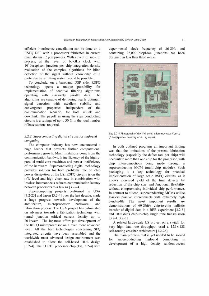
European Roadmap on Superconductive Electronics, Version June 2010 31
efficient interference cancellation can be done on a RSFQ DSP with 4 processors fabricated in current main stream 1.5 μm process. With advent of sub-μm process, at the level of 60 GHz clock with 105 Josephson junction per chip integration density realization of the complex algorithms for blind detection of the signal without knowledge of a particular transmitting system would be possible.
To conclude, on a baseband DSP side, RSFQ technology opens a unique possibility for implementation of adaptive filtering algorithms operating with massively parallel data. The algorithms are capable of delivering nearly optimum signal detection with excellent stability and convergence properties independent of the communication scenario, for both uplink and downlink. The payoff in using the superconducting circuits is a savings of up to 30 % in the total number of base stations required.
3.2.2. Superconducting digital circuits for high-end computing
The computer industry has now encountered a huge barrier that prevents further computational performance growth. Main limitations come from the communication bandwidth inefficiency of the highly-parallel multi-core machines and power inefficiency of the hardware. Superconducting digital technology provides solution for both problems: the on chip power dissipation of the LSI RSFQ circuits is on the mW level and high clock rate in combination with lossless interconnects reduces communication latency between processors to a few ns [3.2-24].
Supercomputing projects performed in USA [3.2-25] and Japan [3.2-4] over the last decade, made a huge progress towards development of the architecture, microprocessor hardware, and fabrication process. The USA project has culminated on advances towards a fabrication technology with tunnel junction critical current density up to 20 kA/cm2. The Japanese effort put development of the RSFQ microprocessor on a even more advanced level. All the best technologies concerning SFQ integrated circuits have been assembled and the worldwide most advanced design environment was established to allow the cell-based HDL design [3.2-4]. The CORE1 processor chip (Fig. 3.2-4) with
experimental clock frequency of 26 GHz and containing 22,000 Josephson junctions has been designed in less than three weeks.
Fig. 3.2-4 Photograph of the 8 bit serial microprocessor Core1γ [3.2-4] (photo - courtesy of A. Fujimaki).
In both outlined programs an important finding
was that the limitations of the present fabrication technology (especially the defect rate per chip) will necessitate more than one chip for the processor, with chip interconnections being made through a superconducting MCM (multi-chip module). Such packaging is a key technology for practical implementation of large scale RSFQ circuits, as it allows increased yield of the final devices by reduction of the chip size, and functional flexibility without compromising individual chip performance. In contrast to silicon, superconducting MCMs utilize lossless passive interconnects with extremely high bandwidth. The most important results are demonstrations of 60 Gbit/s chip-to-chip ballistic transfer of digital data in a BER experiment [3.2-5] and 100 Gbit/s chip-to-chip single tone transmission [3.2-4, 3.2-31].
A related large-scale US project on a switch for very high data rate throughput used a 128 x 128 self-routing crossbar architecture [3.2-26].
The main problem that is yet needed to be solved for superconducting high-end computing is development of a high density random-access

3. Applications of Superconductor Electronics, Digital Electronics 32
memory with speed adequately close to the speed of the logic circuits. All current solutions for the superconducting memory utilize large inductance loops with Josephson junction where information is stored as magnetic flux quanta [3.2-27, 3.2-28, 3.2-29]. This basic principle allows reaching fast memory operation. Switching times in the ps-range, cycle times of 100 ps, and power dissipations of ≈ 120 nW per memory cell have been obtained in 4-kbit RAM blocks based on the RSFQ concept [3.2-27]. However inherit limitation of the memory cell inductance limits the density. The largest superconducting memory chips reported are only 16 kbits.
Current status and future development of the RSFQ circuits for high-end computing are fully covered by the recent Superconducting Technology Assessment published by USA National Security Agency (NSA) [3.2-30]. This assessment is an in-depth examination of RSFQ technologies with the singular objective of determining if a comprehensive roadmap for technology development is possible, aiming for industrial maturity in the 2010-2012 time frame. Main conclusion of the STA report is that there are no significant research issues that need to be resolved on a way towards superconducting supercomputer. The progress in the field will solely depend on aggressive governmental funding.
3.2.3. Interfacing with superconducting detectors and quantum circuits
Because of the ultra low power consumption, the ultra-fast digital superconductive electronics can be integrated on-chip with detectors and superconductive quantum circuits. However, they have resistors as dissipative and noisy elements. The effect of this noise is much smaller than for any other digital electronic family and in some cases, it can be even reduced to meet special requirement of some applications operating in quantum regime.
Detector readout and multiplexing The development of superconducting detectors as
described in section 3.3 has moved toward multi-pixel devices with several hundred active elements,
with the aim of having cameras with resolution that is useful for astronomical observation mapping. The requirement for an ultra low noise and fast readout has raised the problem of integrating lots of SQUID current sensors to realize a multi-pixel device. No other electronics can provide the required circuit complexity and has the potential to work in close vicinity with ultra sensitive sensor elements. The main problems, which have to be addressed, are the complexity of the set-up, and the cost. The systems are currently limited by thermal load and analogue noise, both caused by the readout electronics. Each single pixel requires about 10 wires for control and readout, which limits the total system complexity to less than 100 pixels.
A multiplexed readout seems to be the most promising solution. Both, time-division multiplexing (TDM) and frequency-division multiplexing (FDM) have their advantages [3.2-33, 3.2-34]. Multi-chip modules (MCM), as suggested by NIST [3.2-33], provide an opportunity to test individual bolometers and the multiplexer chip, and thereby increase the yield of assembled cameras.
Fig. 3.2-5 Combination of a 32 SQUID readout multiplexer chip with an 8 × 8 pixel detector array. Only one column of the array is connected. (figure - courtesy of K. D. Irwin)
The superconducting multiplexer chip reduces the
overall system complexity significantly, because of the massive reduction of parallel detector wiring. Fig. 3.2-5 shows a possible MCM configuration suggest by NIST. However, the setup is more

European Roadmap on Superconductive Electronics, Version June 2010 33
Manipulation and readout of quantum circuits complex and additional interferences can degrade the system performance. On the way towards a reliable and scalable
quantum computer, superconducting qubits are promising candidates. On-chip control and readout is a key component to obtain the requested performance. Ideally, the qubits must operate at very low temperature, in an environment with low dissipation to preserve the coherent behaviour, with control and readout circuit placed as close as possible, preferably integrated on-chip [3.2-36]. These requirements are fulfilled by single-flux-quantum digital circuits, which are fast, scalable, require a very low power and share the same Josephson junctions as the same active elements [3.2-37].
The integration of the readout SQUID and the bolometer on the same wafer simplifies the wiring drastically [3.2-34] and the complete device is smaller because of the better integration of all components. Fig. 3.2-6 shows a layout of a hybrid implementation combining the detector and the readout SQUID, developed at IPHT Jena. Additionally, merging the manufacturing technologies promises to simplify the fabrication process. Since the total power dissipation should be less than 1 mW, it might even be possible to fabricate a complete monolithic IC that incorporates both the detector focal plane array and the superconducting readout electronics. Such a chip would normally operate at T = 4.2 K, although it should operate equally well at the reduced temperatures below 1 K, typical for many detectors.
Fig. 3.2-7 Concept for RSFQ control and readout circuits for interfacing a flux qubit [3.2-37].
At very low temperature the tolerable dissipated
power is severely limited by the low refrigerating power of dilution refrigerators close to the base temperature. As a result, building an on-chip RSFQ circuit to control and read out qubits requires a new optimization procedure, a new layout design and a new fabrication process [3.2-38].
Fig. 3.2-6 Layout of one bolometer pixel with the integrated first-stage SQUID on the right hand side. This cell fits on a hexagonal grid of about 4 mm side length (IPHT).
3.2.4. Impact of superconducting digital circuits and outlook on future development
The optimal solution would be a digital multiplexer and digital readout electronics for superconducting sensor arrays, digitizing the signal in the cryogenic environment. This concept offers significant advantages in terms of reduced noise and increased flexibility, particularly as the arrays become larger. Similar to present digital cameras CCD sensors, the data interface of such a system will be a serialized digital output for an array of many detectors.
Due to the necessity of cooling to 4 K, application of RSFQ technology is only motivated for tasks that are impossible or ineffective using semiconductors. Currently even with the moderate integration density available in today's fabrication technology, low-power signal and data processors and switches with

3. Applications of Superconductor Electronics, Digital Electronics 34
Tab. 3.2-1 Evaluation summary of one particular application field
Open questions Expected impact Development status today Low risk development steps
General physical limits
700 GHz clock frequency of a static divider
Advanced process100 GHz
Nb gap of 700 GHz
High density memory Quality of service improve in telecommunication systems
Bias current recycling 35 GHz clock frequency of LSI circuit 9 metal layers Flux trapping 104 Josephson junction yieldable integration density
0.5 μm feature size
Thermal jitter Petaflop computing
60 GHz chip-to-chip communication
no research issues required
how can existing question marks be removed
All Digital Receiver, Hypres Inc USA New architectures and devices
speed equivalent to 20 to 40 GHz clock frequency appear realistic. This technology status makes possible demonstrations and various niche applications in (predominantly military) communications, and perhaps also in signal processing and switching for commercial wireless networks. Were it possible to penetrate the commercial wireless communication community, a sizable niche market could develop. Massive serial computing and data switching appears possible in principle, but would require a dramatic increase in the level of resources, both manpower and funding, compared to what this technology enjoyed in the past. This would lead to the creation of the necessary professional infrastructure and thus to the removal of existing technological obstacles.
RSFQ outperforms all existing digital technology in speed and power. However, RSFQ technology also has several limitations. Some arise from the relative immaturity of the technology, and some are inherent. The major maturity-related problem is yieldable integration density.
In all applications advanced processing technology will allow more complex circuits on the chips. Still larger circuits must use the multi/chip module (MCM) technique. Regarding supercomputing, only technological breakthroughs and the infusion of sizable and stable financing could enable true VLSI on chip.
Inherent limitations of superconducting digital circuits include flux trapping, bias current distribution, noise-induced jitter and heavy use of
active elements for signal propagation. Altogether these factors limit complexity of reliable circuits. Architectures and logic most suitable for processing SFQ pulse should be further explored.
Hybrid technologies, e.g., involving CMOS, should be chosen to take advantage of the strengths of superconducting logic, while sidestepping the weaknesses. Further work is needed on two-way hybrid interfaces with room temperature circuitry, and on integration with suitable 4 Kelvin cryo-coolers.

European Roadmap on Superconductive Electronics, Version June 2010 35
Tab. 3.2- 2. Timeline for Digital Electronics Development
Digital SE
Basic R&D
Basic R&D
Basic R&D
Basic R&D
Applied R&D
Applied R&D
Applied R&D
Applied R&D
Applied R&D
First Appl.
First Appl.
First Appl.
First Appl.
First Appl.
Mature Appl.
Mature Appl.
Mature Appl.
Mature Appl.
2010 2011 2012 2013 2014 2015 2016 2017 2018 2019 2020
Sensor Interface
Memory
Microprocessor
DSP
ADCs
[3.2-12] I. V. Vernik, D. E. Kirichenko, T. V. Filippov, A. Talalaevskii, A. Sahu, A. Inamdar, A. F. Kirichenko, D. Gupta, O. A. Mukhanov, IEEE Trans. Appl. Supercond, vol. 17, no. 2, pp. 442, 2007.
[3.2-13] D. Gupta, T. V. Filippov, A. F. Kirichenko, D. E. Kirichenko, I. V. Vernik, A. Sahu, et al, IEEE Trans. Appl. Supercond, vol. 17, no. 2, pp. 430, 2007.
References
[3.2-14] O.A. Mukhanov, D. Kirichenko, I.V. Vernik, T.V. Filippov, A. Kirichenko, R. Webber, V. Dotsenko, A. Talalaevskii, J.C. Tang, A. Sahu, P. Schevchenko, R. Miller, S.B. Kaplan, S. Sarwana, D. Gupta, IEICE Trans. Electron. 91E-C, 293-305, 2008.
[3.2-1] K.K. Likharev and V.K. Semenov, IEEE Trans. On Appl. Supercond., vol.1, no.1, p.3, 1991.
[3.2-2] W. Chen, A. V. Rylyakov, Vijay Patel, J. E. Lukens, K. K. Likharev, Appl. Phys. Lett., vol. 73, pp. 2817, 1998.
[3.2-3] Y. Hashimoto, S. Yorozu, and T. Satoh, Appl. Phys. Lett., vol. 87, no. 022502, pp. 022 502:2-3, July 2005 [3.2-15] A. Inamdar, A. Talalaevskii, A. Sahu, D. E. Kirichenko,
T. V. Filippov, D. Gupta, to be published in IEEE Trans. Appl. Supercond, 2008.
. [3.2-4] S. Yorozu, Y. Kameda, Y. Hashimoto, and S. Tahara, IEEE
Trans. Appl. Supercond., vol. 13, no. 2, pp. 450-453, June 2003. [3.2-16] Q. P. Herr, D. L. Miller, A. A. Pesetski, J. X. Przybysz, to
be published in IEEE Trans. Appl. Supercond, 2009. [3.2-5] Q. Herr, A. Smith, and M. Wire, Applied Physics Letters., vol. 80, no. 2, pp. 3210-12, 2002. [3.2-17] A. A. Pesetski, Q. P. Herr, D. L. Miller, J. X. Przybysz, to
be published in IEEE Trans. Appl. Supercond, 2009. [3.2-6] H. Hayakawa, N. Yoshikawa, S. Yorozu, and A. Fujimaki, Proceedings of the IEEE, vol.92, no.10, pp.1549-1563, Oct. 2004.
[3.2-18] D. Gupta, Y. Zhang, Appl. Phys. Lett. 76, 3819, 2000. [3.2-19] I. Kataeva, H. Zhao, H. Engseth, E. Tolkacheva, and A.
Kidiyarova-Shevchenko, IEEE. Trans. Appl. Supercond., vol.15, no.2, p.405, 2005.
[3.2-7] I. V. Vernik, D. E. Kirichenko, V. V. Dotsenko, R. Miller, R. J. Webber, P. Shevchenko, A. Talalaevskii, D. Gupta, and O. A. Mukhanov, Supercond. Sci. Technol., vol. 20, no. 11, pp. S323-S327, November 2007.
[3.2-20] www.hypres.com[3.2-21] H. Zhao, T. Ottosson, E. Strom, and A. Kidiyarova-
Shevchenko, Vehicular Technology Conference, 2004. VTC2004-Fall. 2004 IEEE 60th, vol.3, pp.1919-923, 2004.
[3.2-8] K.V. Ramachandra, CRC Press, 2000. [3.2-9] A.Y. Kidiyarova-Shevchenko, K. Platov, T. Ottosson, and
E. Strom, Supercond. Sci. and Technol., vol.15, pp.126-132, 2002.
[3.2-22] I. Kataeva, H. Engseth, and A. Kidiyarova-Shevchenko, IEEE. Trans. Appl. Supercond., vol.17, p.486, 2007.
[3.2-23] H. Engseth, R. Webber, and S. Kaplan, “Cryocooler interface for the RSFQ DSP," EXT. Abs. ISEC'07, 2007.
[3.2-10] C. Windpassinger, R.F.H. Fischer, T. Vencel, and J.B. Huber, IEEE Tran. on Wireless Commun., vol.3, p.1305, 2004. [3.2-24] K. Likharev, M. Dorozevets, P. Bunyk, D. Zinoviev,
Physica B: Condensed Matter, vol. 280, no. 1-4, pp. 495-496, 2000.
[3.2-11] Z. Xu and M. Tsatsanis, IEEE Tran. on Commun., vol.49, no.1, pp.180-194, 2001.

3. Applications of Superconductor Electronics, Digital Electronics 36
[3.2-25] M. Dorozevets, P. Bunyk, IEEE. Trans. Appl. Supercond., vol.13, p.446, 2003.
[3.2-26] R.D. Sandell, J.W. Spargo, M. Leung, S.R. Whiteley, IEEE. Trans. Appl. Supercond., vol.9, p.2985, 1999.
[3.2-27] A.F. Kirichenko, S. Sarwana, D.K. Brock, M. Radpavar, IEEE. Trans. Appl. Supercond., vol.11, p.537, 2001.
[3.2-28] S. Nagasawa, H. Hasegawa, T. Hashimoto, H. Suzuki, Supercond. Sci. Technol., vol. 12, pp. 933–936, 1999.
[3.2-29] Q.P. Herr, L. Eaton, Supercond. Sci. Technol., vol. 12, pp. 929–936, 1999.
[3.2-30] NSA Superconducting Technology Assesment available at http://www.nitrd.gov/pubs/nsa/sta.pdf
[3.2-31] Y. Hashimoto, S. Yorozu, T. Satoh and T. Miyazaki, "Demonstration of chip-to-chip transmission of single-flux-quantum pulses at throughputs beyond 100 Gbps," Appl. Phys. Lett., 87, 022502, 2005.
[3.2-32] Y Hashimoto, S Yorozu, Y Kameda, "Development of Cryopackaging and I/O Technologies for High-Speed Superconductive Digital Systems," IEICE Trans. on Electronics, pp. 325-332, 2008.
[3.2-33] J. Yoon, J. Clarke, J.M. Gildenmeister, A.T. Lee, M.J. Myers, P.L. Richards, and J.T. Skidmore, Single “SQUID multiplexer for arrays of low-temperature sensors”, Appl. Phys. Lett. 78, 371, 2001.
[3.2-34] K. D. Irwin, “SQUID multiplexers for transition edge sensors,” Physica C, vol. 368, pp. 203–210, 2002
[3.2-35] T. May, V. Zakosarenko, E. Kreysa,W. Esch, S. Anders, L. Fritzsch, R. Boucher, R. Stolz, J. Kunert, and H.-G. Meyer, “On-Chip Integrated SQUID Readout for Superconducting Bolometers”, IEEE Trans. Appl. Supercond. Vol 15, No. 2, June 2005
[3.2-36] A. Fedorov, A. Shnirman, and G. Schön, “Reading out the state of a flux qubit by Josephson transmission line solitons”, PHYSICAL REVIEW B 75, 224504, (2007)
[3.2-37] M.G. Castellano, L. Grönberg, P. Carelli, F. Chiarello, C. Cosmelli, R. Leoni, S. Poletto, G. Torrioli, J. Hassel and P. Helistö, “Characterization of a fabrication process for the integration of superconducting qubits and rapid-single-flux-quantum circuits“, Supercond. Sci. Technol. 19 (2006) 860–864
[3.2-38] J. Hassel, P. Helisto, H. Seppa, J. Kunert, L. Fritzsch, and H. G. Meyer, “Rapid single flux quantum devices with selective dissipation for quantum information processing“, Appl. Phys. Lett. 89, 182514 (2006)

European Roadmap on Superconductor Electronics, Version June 2010 37
3.3. Magnetic Field Sensors and ultra-low Noise Amplifiers
3.3.1. Introduction Superconducting quantum interference devices
(SQUIDs) are the most sensitive detectors of magnetic flux variations. In principle, every physical quantity which can be converted into magnetic flux can be measured with SQUIDs, e.g. magnetic induction or electrical current. SQUIDs are fabricated using sophisticated thin-film deposition and patterning techniques and have to be cooled to operational temperatures of about 4 K (Low-Tc SQUIDs, LTS SQUIDs) or about 77 K (High-Tc SQUIDs, HTS SQUIDs), which correspond to the boiling temperatures of liquid helium or liquid nitrogen, respectively. To operate the SQUIDs, sensitive and sometimes complex read-out electronics are required. Several different SQUID read-out schemes have been developed. Their limits and trends will be discussed briefly in this section.
Because of the high sensitivity of SQUIDs their full potential can be exploited only if electromagnetic interference is suppressed effectively. SQUID magnetometer systems including noise suppression and cryogenics are fairly expensive and, therefore, they will be utilized only in those applications where ultimate sensitivity is needed. The main application fields are described in this chapter, with a focus on novel measuring techniques. For a more detailed description of applications mentioned in this roadmap please see [3.3-1].
3.3.2. SQUID devices and concepts
3.3.2.1. Dc and rf SQUIDs Dc SQUIDs consisting of a superconducting loop
with two Josephson junctions are magnetic flux (Φ)-to-voltage (V) converters with a non-linear, periodic V-Φ characteristic. Rf SQUIDs with only one junction in the loop have a similar characteristic but the output voltage is in the MHz or even GHz regime. Although in the past rf SQUIDs were widely used, more recently dc SQUIDs have become the most (commercially) exploited SQUID type, especially in
multichannel systems. For systems where a high dynamic range and a wide bandwidth are required dc SQUIDs dominate the field.
An overview of SQUID research and development in Europe has recently been published by Braginski and Donaldson [3.3-2]
3.3.2.2. Relaxation Oscillation SQUIDs Relaxation Oscillation SQUIDs (ROSs) or Double
ROSs (DROSs) based on dc SQUIDs with hysteretic I-V characteristics are an alternative to standard dc SQUIDs. They exhibit very high transfer coefficients ∂V/∂Φ allowing the use of simplified direct-coupled read-out electronics. DROSs have been developed and intensively investigated by the Twente group and are used e.g. in biomagnetic multi-channel systems and gravitational wave detectors [3.3.-3]. The Korean metrology institute KRISS manufactures a considerable number of magnetoencephalography systems using this SQUID type [3.3.-4] which are widely distributed in Asia.
3.3.2.3. Digital SQUIDs In today’s SQUID systems, the output signal of
analog SQUID read-out electronics is digitized using high-resolution A/D converters. A lot of research has focused on developing completely digitized feedback loops where the error signal of the SQUID is digitized, then integrated by means of a digital signal processor and fed back into the SQUID via high-resolution D/A conversion. Furthermore, the dynamic range of the SQUID system can be increased easily by implementing a flux quanta counting procedure in the digital SQUID electronics utilizing the periodicity of the SQUID magnetic flux-to-voltage transfer function. It should be mentioned here, that flux quanta counting can be used for analog SQUID feedback loops as well.
The digital SQUID concept is particularly attractive if it is combined with RSFQ techniques. In this case the feedback loop can be set up on chip at cryogenic temperatures avoiding the transmission line delay between SQUID and room temperature electronics, enabling very fast SQUID systems [3.3.-5]. Low-temperature FLL schemes allowing for wide bandwidth operation have been recently realized using analog SQUIDs (see chapter 3.3.4).

3. Application of Superconductor Electronics, Magnetic Field Sensors and ultra-low Noise Amplifiers 38
3.3.2.4. SQIFs Superconducting Quantum Interference Filters
(SQIFs) are novel devices consisting of arrays of individual SQUID loops of statistically varying loop size. In contrast to conventional dc SQUIDs, the voltage-flux characteristics of such a SQIF is no longer a periodic one but has a single peak which allows absolute magnetic flux measurements. This opens novel applications in magnetometry [3.3-16]. It has been demonstrated that these devices can be realized even with HTS technology on bicrystal substrates [3.3-17]. Furthermore, these devices are attractive for low-noise amplifiers. Following on from the concept of superposition of SQUID characteristics with different periodicity in a SQIF, SQUID arrays with different signal coupling to the individual SQUID loops of equal size have been used in absolute dc current sensors [3.3-18].
3.3.2.5. HTS and LTS SQUIDs As mentioned above, HTS and LTS SQUIDs use
different superconducting materials in the SQUID fabrication process. In the 90s a lot of effort was put worldwide into the development of an appropriate junction technology using HTS thin-films. Although industrial fabrication of high quality HTS thin-films could be realized even on large substrates (THEVA), an adequate junction fabrication process allowing the reproducible fabrication of a number of junctions in any location on a (cheap) wafer is still missing. The combination of thin-film devices with superconducting wire-wound antennas or leads, which is routinely used in Nb-based LTS technology, is not available for HTS which is a serious restriction for a number of applications. Aging of HTS sensors is still a problem.
The operation of HTS SQUIDs even in a moderately noisy environment (as opposed to one with realistic noise levels) is much more challenging than with LTS SQUIDs because of flux trapping in the films. More complicated read-out schemes (e.g. ac biasing techniques for dc SQUIDs) have to be applied. In contrast to the situation for LTS SQUID where dc SQUIDs dominate the field, the rf SQUID concept is very attractive for HTS SQUIDs because of its design simplicity – only one junction, no bonding wires. Despite the fact, that most aspects of
the properties of HTS SQUIDs (in particular if they are based on YBCO) have been intensively investigated and that the magnetic field resolution demonstrated is sufficient for many applications, HTS SQUIDs have not reached the performance initially predicted. A magnetic field sensitivity of <50 fT/Hz is typically achieved for single layer SQUIDs fabricated on 10 mm x 10 mm substrates and values <30 fT/Hz have been demonstrated. For comparison, with LTS SQUIDs values of. around 1 fT/Hz can be routinely achieved on the same chip size using Nb-based multilayer techniques. Currently, only measuring systems equipped with one or a few sensors seem to make sense, e.g. for NDE. HTS SQUIDs are offered commercially only by a few companies (e.g. dc SQUIDs: [3.3-6], rf SQUIDs: [3.3.-7]). A good overview of HTS SQUID applications can be found in [3.3-8]. The recent development of alternative more or less competitive sensors (e.g. optical magnetometers) is also affecting this situation.
Nowadays, LTS SQUID microfabrication is usually based on an all refractory Nb/AlOx/Nb thin-film technology. There are some companies fabricating thin-films or complete superconducting devices to costumer’s specifications. In Europe the Fluxonics Foundry provides such services for the community [3.3-9].
Standard integrated dc SQUID magnetometers or gradiometers with high sensitivity are commercially available. In contrast to HTS SQUIDs, LTS SQUID current sensors offer the possibility to build magnetometers and gradiometers of high flexibility using wire-wound pick-up coils. Superconducting LTS bonding technology is routinely mastered.
3.3.2.6. SQUID amplifiers The SQUID amplifier is an enabling technology
for a number of basic research experiments, e.g. read-out of radiation detectors, the detection of gravitational waves, highly sensitive NMR and susceptometry at low and ultra-low temperatures. When detecting extremely small amounts of energy in such experiments, SQUIDs have to be operated in complex low-temperature cryostats. This requires sensors which are very robust against electromagnetic interference. Meanwhile, extremely balanced

European Roadmap on Superconductor Electronics, Version June 2010 39
gradiometric designs enable unshielded operation of SQUID current sensors, which can be mounted for exampledirectly on the low-temperature platform of mK-cryostats [3.3-10].
In general, one sensor type cannot fit all these applications. For very specific experiments, SQUIDs have to be developed and designed for the particular experimental setup. State-of-the-art SQUID amplifiers are complex devices with up to several hundred of single SQUIDs and a number of auxiliary components and supporting circuits such as filters and current limiters integrated on chip offering unique performance (see Figure 3.3-1).
Customized devices such as these are commercially available, from European [3.3-11, 3.3-12] and North American [3.3-6, 3.3-28, 3.3-29] suppliers.
So, it is of great importance for future research activities or projects in the European Society to have a superconducting technology available which enables the fabrication of such elaborate SQUID designs (see also [3.3-9]).
Fig. 3.3-1. Layout (a) and basic circuit diagram (b) of an integrated 2-stage LTS SQUID current sensor (PTB) .
3.3.2.7. Parametric SQUID amplifiers Development activities for the readout of large-
format arrays of radiation detectors have triggered renewed interest in non-hysteretic rf SQUIDs or microwave SQUIDs, sometimes called ac SQUIDs, which can be used as parametric amplifiers. Its concept - a flux-variable, non-hysteretic inductor formed by an undamped Josephson junction interrupting a superconducting loop - was originally described by K.Likharev [3.3-13]. In particular, in the context of low-temperature superconducting detector readout, parametric SQUID amplifiers are an appealing approach [3.3-14, 3.3-15]. Like traditional rf SQUIDs, an ac SQUID is read out in a resonant tank circuit, enabling parametric amplification at
microwave frequencies. In doing so, the parametric SQUID amplifier benefits from the excellent noise and dynamics performance of state-of-the-art high electron mobility transitor (HEMT) amplifiers. Moreover, frequency domain multiplexing is natural. The parametric SQUID amplifier is purely reactive, i.e., signals can be sensed without dissipating any power in the SQUID itself. This is of practical importance as cooling power at very low operating temperatures is limited.
3.3.3. SQUID Applications
3.3.3.1. Medical and biochemical diagnostics The ultimate sensitivity of SQUID magnetometers
enabling detection of magnetic fields as weak as a few fT gives rise to research activities in biomagnetism, nuclear magnetic resonance imaging, magnetic marker based methods and others. Although biomagnetic measurements, mainly magneto-cardiography (MCG) and magnetoencephalography (MEG), can be performed using (commercially available) multi-channel SQUID systems, novel techniques like low-frequency nuclear magnetic resonance imaging (lf-MRI) and magnetic marker based methods require novel SQUID sensors which are extremely robust against interfering magnetic fields. Therefore, the development of these methods and adequate instrumentation must be accompanied by developing novel SQUID sensors as well in order to become of practical clinical importance.
Biomagnetism Magnetocardiography A lot of work has focussed on the introduction of
MCG to clinical practice. However, although it has been demonstrated that MCG provides at least the same information obtained by electrocardiography (ECG) and additional information can be obtained, MCG is yet to become a widely accepted clinical tool. A major problem is the availability of reasonably priced, easy to use and high throughput imaging systems that would e.g. allow for accurate cardiac risk analysis.
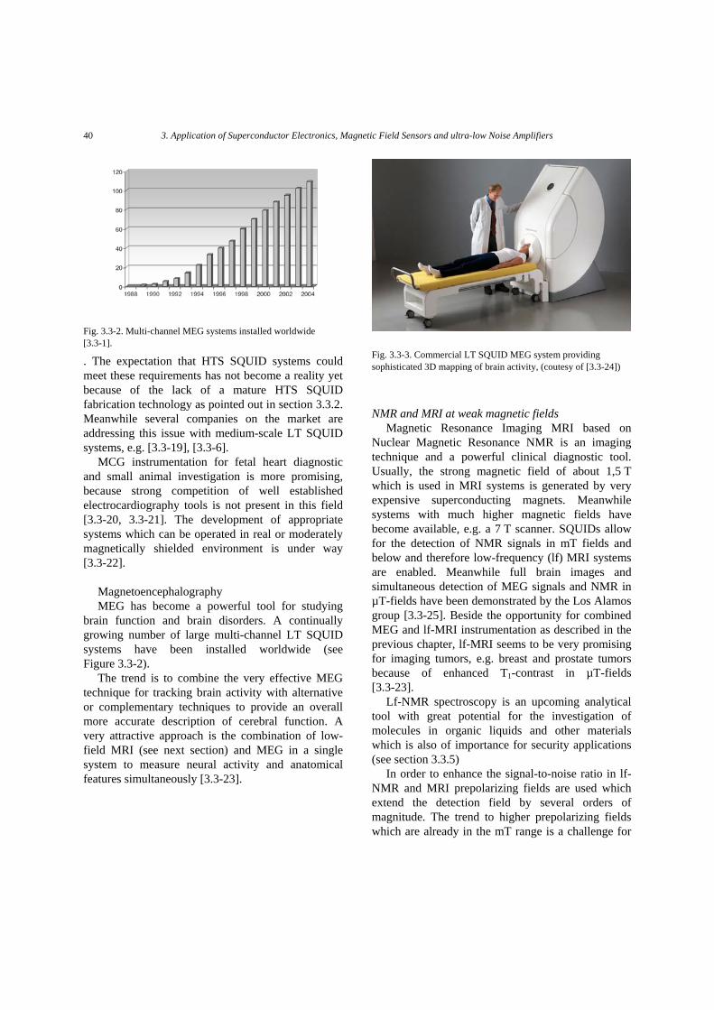
3. Application of Superconductor Electronics, Magnetic Field Sensors and ultra-low Noise Amplifiers 40
Fig. 3.3-2. Multi-channel MEG systems installed worldwide [3.3-1].
. The expectation that HTS SQUID systems could meet these requirements has not become a reality yet because of the lack of a mature HTS SQUID fabrication technology as pointed out in section 3.3.2. Meanwhile several companies on the market are addressing this issue with medium-scale LT SQUID systems, e.g. [3.3-19], [3.3-6].
MCG instrumentation for fetal heart diagnostic and small animal investigation is more promising, because strong competition of well established electrocardiography tools is not present in this field [3.3-20, 3.3-21]. The development of appropriate systems which can be operated in real or moderately magnetically shielded environment is under way [3.3-22].
Magnetoencephalography MEG has become a powerful tool for studying
brain function and brain disorders. A continually growing number of large multi-channel LT SQUID systems have been installed worldwide (see Figure 3.3-2).
The trend is to combine the very effective MEG technique for tracking brain activity with alternative or complementary techniques to provide an overall more accurate description of cerebral function. A very attractive approach is the combination of low-field MRI (see next section) and MEG in a single system to measure neural activity and anatomical features simultaneously [3.3-23].
Fig. 3.3-3. Commercial LT SQUID MEG system providing sophisticated 3D mapping of brain activity, (coutesy of [3.3-24])
NMR and MRI at weak magnetic fields Magnetic Resonance Imaging MRI based on
Nuclear Magnetic Resonance NMR is an imaging technique and a powerful clinical diagnostic tool. Usually, the strong magnetic field of about 1,5 T which is used in MRI systems is generated by very expensive superconducting magnets. Meanwhile systems with much higher magnetic fields have become available, e.g. a 7 T scanner. SQUIDs allow for the detection of NMR signals in mT fields and below and therefore low-frequency (lf) MRI systems are enabled. Meanwhile full brain images and simultaneous detection of MEG signals and NMR in µT-fields have been demonstrated by the Los Alamos group [3.3-25]. Beside the opportunity for combined MEG and lf-MRI instrumentation as described in the previous chapter, lf-MRI seems to be very promising for imaging tumors, e.g. breast and prostate tumors because of enhanced T1-contrast in µT-fields [3.3-23].
Lf-NMR spectroscopy is an upcoming analytical tool with great potential for the investigation of molecules in organic liquids and other materials which is also of importance for security applications (see section 3.3.5)
In order to enhance the signal-to-noise ratio in lf-NMR and MRI prepolarizing fields are used which extend the detection field by several orders of magnitude. The trend to higher prepolarizing fields which are already in the mT range is a challenge for

European Roadmap on Superconductor Electronics, Version June 2010 41
the design and technology of the SQUID based sensors used in these experiments because flux trapping in superconducting structures and superconducting thin films are limiting factors. The sensors are not required to operate during the application of the prepolarizing field but have to be switched to the sensing mode as quick as possible immediately after the prepolarizing field is switched off.
Fig. 3.3-4. Low-field NMR setup (PTB). The polarization field generated magnetization along the y axis by the large Helmholtz coils. After switching off the polarization field ,sample magnetization begins to precess about the z axis of the detection field which is produced by a small field coil containing the sample below the cryostat. The LF-NMR setup is operated in a magnetically shielded room.
Magnetic Shielding Another limiting factor especially for high
resolution lf-NMR and MRI is the suppression of magnetic interference. Usually magnetically shielded rooms consisting of several layers of mu-metal are used. There some European suppliers and very heavily shielded rooms available for experiments, but not only the shielding factor is of importance. For high-resolution spectroscopy where the natural line-width of molecules will be exploited the residual field in the shielding has to be very homogeneous. This requires a very sophisticated knowledge about the
magnetization processes in mu-metal and the development of effective demagnetization procedures.
Heavily shielded mu-metal rooms are very expensive and have high demands on the construction site. So, the development of alternative shielding methods is essential for commercial systems. Active field compensation and superconducting shields are possible approaches in combination with effective electronical and software noise reduction [3.3-22].
Magnetic Nanoparticles In recent years, there has been an increasing
interest in investigating the potential of magnetic nanoparticles that are dressed with bio-molecules such as antibodies or antigens for Immunoassays [3.3-29, 3.3-30]. Different magnetic relaxation (MRX) phenomena which are detected with the SQUID magnetometers can determine if there has been a reaction or not with a resolution that is presently a factor of 10 better than the commonly used ELISA (Enzyme-Linked Immunosorbent Assay). The expected performance of these and other SQUID based systems have a resolution of maybe two orders of magnitude better than ELISA. Furthermore, it is proposed to use SQUIDs to determine the possible spread of cancer cells in the lymphatic system by using tagged magnetic nanoparticles and one could envision drug delivery agents tagged by magnetic particles where the drug accumulation could be verified by SQUID detection once they reach their targets. Both, LTS and HTS devices are of interest here, because such measurement systems require only a small number of sensors. The trend goes to high-throughput systems and instrumentation which can achieve a spatial resolution of MRX Even for those applications sensors that can resist large prepolarizing magnetic fields are required.
Currently, the bottleneck to the application of this diagnostic technique is not the status of the magnetic sensors but the availability of adequate functionalized magnetic nanoparticles.
3.3.3.2. Read-out of Radiation Detectors SQUIDs are widely used to read out a certain class
of highly sensitive detectors for cryogenic photon
3. Application of Superconductor Electronics, Magnetic Field Sensors and ultra-low Noise Amplifiers 42
detection. These detectors are namely super-conducting transition edge sensors (TESs), magnetic microcalorimeters (MMCs) and hot-electron bolometers (HEBs) [3.3-31]. Here, SQUIDs are used as sensitive and fast low-power current sensors which are compatible with the very low (< 1 K) operating temperatures of TESs and MMCs. Furthermore, a SQUID current sensor with a superconducting input coil is very well suited to obtain impedance-matching to the typically low impedance TESs and MMCs.
Large ground based, air-borne, and space telescopes will be equipped with large multi-pixel sensor arrays of up to several thousands elements which requires SQUID-multiplexing techniques. Several multiplexing schemes are currently under test. Sensor systems for sub-millimeter, infrared and X-ray detection are under construction.
These applications are strong drivers for the development of integrated SQUID read-out circuits with increasing complexity. Novel concepts are under investigation to meet the extreme requirements regarding the dynamic range of the SQUID based read-out of superconducting photon detectors, e.g. TESs. One approach is to operate conventional semiconductor based electronics near the amplifier SQUID at low-temperature. The drawback of this solution is the increased power dissipation at the low-temperature level which has to be compensated by cooling, typically about 10 mW per channel, but even values below 1 mW could be achieved with cryogenic bipolar transistor amplifiers [3.3-32]. This is in particular a limiting factor when using cryocoolers. A more recent approach is a SQUID based linearization scheme. When this so-called current-sampling feedback [3.3-33] or output current feedback [3.3-34] is integrated on the amplifier SQUID chip, a drastically increased dynamic range is obtained at the expense of a moderate increase in power dissipation (ca. 10 nW).
3.3.3.3. Security applications THz cameras similar to the astrophysical
instrumentation described in the previous chapter are promising tools for industrial and security applications.
Another extremely sensitive future screening technology is based on ultra-low field magnetic
resonance imaging (MRI), which detects the magnetic changes of individual materials at the molecular level. The data are compared with a database and allows the differentiation and identification of many materials that may be packaged together or separately for instance in carry on luggage. The goal is rapid hazard and narcotics identification even if they are enclosed in luggage or closed containers as well as increased automation of luggage inspection at transport centres and airports [3.3-35].
It is very important to initiate European research activities or projects to develop this enabling technology which will be tested for the first time at Albuquerque airport in 2009.
3.3.3.4. Geophysical Sounding and Archeology SQUIDs and their extreme sensitivity to magnetic
field and its gradients have important applications in geophysics. Two main techniques have been developed to date. Of these, passive methods map the Earth’s magnetic field and anomalies. These anomalies are directly (e.g. iron, chromium, diamonds) or indirectly (e.g. platinum, gold) related to minerals, natural oil and gas deposits, volcanic dykes and other structures and the knowledge is used for exploration and mine planning and improves the efficiency of natural resources usage. In addition, unexploded ordnances, shallow underground landfill or ancient remains (archeology) can also be detected [3.3-36].
The goal of active methods is to provide information about conductive layers below the surface for depths of up to a few kilometers. Excitations in different frequency ranges (e.g. MT, TEM, AMT, CSAMT) are used to determine the electrical conductivity of Earth’s rocks and sediments in order to understand tectonic processes and geologic structures as well as other environmental aspects like ground water and shallow disposal sites. Customized LTS and HTS SQUID TEM systems are commercially available [3.3-11].
LTS SQUID sensors play an important role in the field of portable gravity gradiometers as detectors for movement of test masses, and this is of great interest in geophysics today as a way of measuring density

European Roadmap on Superconductor Electronics, Version June 2010 43
differences in the surface. Worldwide there are no appropriate systems available today.
Fig. 3.3-4. Air borne SQUID system for geophysical sounding (IPHT Jena).
3.3.3.5. Nondestructive evaluation Nondestructive evaluation of materials, e.g.
aircraft parts, nuclear plants, steel reinforced concrete structures, electronic chips, is a challenging field for SQUID based instruments. The high sensitivity and wide dynamic range of SQUIDs permit faults, cracks, electrical defects, impurities etc to be detected; the presence of which can cause malfunction or even catastrophic fatigue failures. Active techniques, such as eddy current scanning methods and passive detection techniques such as detection of metallic particles in food are being investigated [3.3-37].
HTS SQUIDs have been intensively tested in these applications because such NDE systems are equipped only with a few sensors. Nevertheless, the need of cryogenic equipment is still an obstacle for practical use. Practical LTS SQUID based eddy current NDE systems and services are meanwhile provided on a commercial basis [e.g. 3.3-38].
3.3.3.6. SQUIDs for nanoscience and microscopy Science and industry demand ever more sensitive
measurements on objects in the micro- and nanoscale, as exemplified by spintronics, nanoelectromechanical systems, spin-based quantum information processing, where single electron spin detection poses a grand
challenge. NanoSQUIDs are being investigated to address these issues but it is quite difficult to realize such structures because the well established Josephson junction techniques exploited in state-of-the-art SQUIDs cannot be easily adopted to these nano-scaled devices [3.3-45].
The passive detection of the magnetization of the smallest structures, or actively generated magnetic fields in micro- and sub-micro-structures, by small SQUID devices is called SQUID microscopy [3.3-39]. If the sample under investigation is at room temperature, these instruments require sophisticated cryostats which allow for a small sensor-to-sample distance. This distance is the limiting factor for spatial resolution even if micro-SQUIDs are used. HTS SQUIDs are well suited for microscopes because the cooling of these devices in small distance to the room temperature sample is much easier compared to LTS SQUIDs. They have great potential in particular for magnetic nanoparticle characterization using MRX (see chapter Magnetic nanoparticles).
Fig. 3.3-5. Commercial LT SQUID NDE system for defect inspection of materials (courtesy of [3.3-38])
3.3.3.7. Measurement techniques and metrology Precise measurements have been the domain of
SQUIDs for many years and the current progress in nanoscale science and technology will open the door for new applications of these sensors. A detailed discussion of the limitations placed by the SQUID on
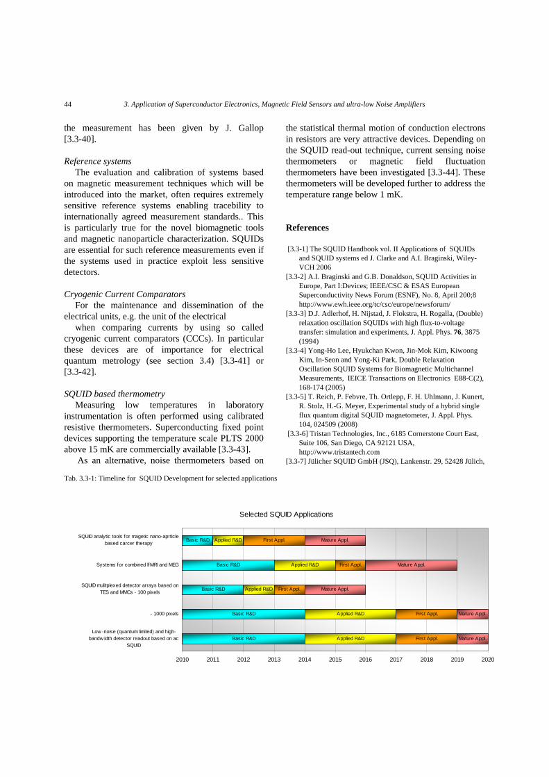
3. Application of Superconductor Electronics, Magnetic Field Sensors and ultra-low Noise Amplifiers 44
the measurement has been given by J. Gallop [3.3-40].
Reference systems The evaluation and calibration of systems based
on magnetic measurement techniques which will be introduced into the market, often requires extremely sensitive reference systems enabling tracebility to internationally agreed measurement standards.. This is particularly true for the novel biomagnetic tools and magnetic nanoparticle characterization. SQUIDs are essential for such reference measurements even if the systems used in practice exploit less sensitive detectors.
Cryogenic Current Comparators For the maintenance and dissemination of the
electrical units, e.g. the unit of the electrical when comparing currents by using so called
cryogenic current comparators (CCCs). In particular these devices are of importance for electrical quantum metrology (see section 3.4) [3.3-41] or [3.3-42].
SQUID based thermometry Measuring low temperatures in laboratory
instrumentation is often performed using calibrated resistive thermometers. Superconducting fixed point devices supporting the temperature scale PLTS 2000 above 15 mK are commercially available [3.3-43].
As an alternative, noise thermometers based on
the statistical thermal motion of conduction electrons in resistors are very attractive devices. Depending on the SQUID read-out technique, current sensing noise thermometers or magnetic field fluctuation thermometers have been investigated [3.3-44]. These thermometers will be developed further to address the temperature range below 1 mK.
References
[3.3-1] The SQUID Handbook vol. II Applications of SQUIDs and SQUID systems ed J. Clarke and A.I. Braginski, Wiley-VCH 2006
[3.3-2] A.I. Braginski and G.B. Donaldson, SQUID Activities in Europe, Part I:Devices; IEEE/CSC & ESAS European Superconductivity News Forum (ESNF), No. 8, April 200;8
http://www.ewh.ieee.org/tc/csc/europe/newsforum/ [3.3-3] D.J. Adlerhof, H. Nijstad, J. Flokstra, H. Rogalla, (Double)
relaxation oscillation SQUIDs with high flux-to-voltage transfer: simulation and experiments, J. Appl. Phys. 76, 3875 (1994)
[3.3-4] Yong-Ho Lee, Hyukchan Kwon, Jin-Mok Kim, Kiwoong Kim, In-Seon and Yong-Ki Park, Double Relaxation Oscillation SQUID Systems for Biomagnetic Multichannel Measurements, IEICE Transactions on Electronics E88-C(2), 168-174 (2005)
[3.3-5] T. Reich, P. Febvre, Th. Ortlepp, F. H. Uhlmann, J. Kunert, R. Stolz, H.-G. Meyer, Experimental study of a hybrid single flux quantum digital SQUID magnetometer, J. Appl. Phys. 104, 024509 (2008)
[3.3-6] Tristan Technologies, Inc., 6185 Cornerstone Court East, Suite 106, San Diego, CA 92121 USA, http://www.tristantech.com
[3.3-7] Jülicher SQUID GmbH (JSQ), Lankenstr. 29, 52428 Jülich,
Tab. 3.3-1: Timeline for SQUID Development for selected applications
Selected SQUID Applications
Basic R&D
Basic R&D
Basic R&D
Basic R&D
Basic R&D
Applied R&D
Applied R&D
Applied R&D
Applied R&D
Applied R&D
First Appl.
First Appl.
First Appl.
First Appl.
First Appl.
Mature Appl.
Mature Appl.
Mature Appl.
Mature Appl.
Mature Appl.
Low -noise (quantum limited) and high-bandw idth detector readout based on ac
SQUID
- 1000 pixels
SQUID mulitplexed detector arrays based onTES and MMCs - 100 pixels
Systems for combined lfMRI and MEG
SQUID analytic tools for magetic nano-aprticlebased carcer therapy
2010 2011 2012 2013 2014 2015 2016 2017 2018 2019 2020

European Roadmap on Superconductor Electronics, Version June 2010 45
[3.3-28] Quantum Design, http://www.jsquid.com 6325 Lusk BoulevardGermany ,San Diego, CA 92121-3733, USA; htttp://www.qdusa.com [3.3-8] High Temperature Superconductivity 2, ed. A.V. Narlikar,
Springer 2004 [3.3-29] E.R. Flynn, H.C. Bryant, A biomagnetic system for in vivo cancer imaging, Phys. Med. Biol. 50 (2005) 1273–1293 [3.3-9] The Fluxonics Foundry, http://www.fluxonics-foundry.de
[3.3-30] L. Trahms, Biomedical applications of magnetic nanoparticles. In: Colloidal Magnetic Fluids, Lecture Notes in Physics 763 (ed. by S. Odenbach), Springer, pp 327-358.(2009)
[3.3-10] D. Drung, C. Assmann, J. Beyer, A. Kirste, M. Peters, F. Ruede, and Th. Schurig; Highly sensitive and easy-to-use SQUID sensors ; IEEE Trans. Appl. Supercond. 17, 699 (2007)
[3.3-31] Ch Enss (Ed.), Cryogenic Particle Detection Topics Appl.. Phys. 9, 63-149 (Berlin Heidelberg: Springer) 2005
[3.3-11]Supracon AG, Wildenbruchstr. 15, 07745 Jena Germany, http://www.supracon.de
[3.3-32] M. Kiviranta, Use of SiGe bipolar transistors for cryogenic readout of SQUIDs, Supercond. Sci. Technol. 19 1297 (2006)
[3.3-12] Magnicon GbR, Lemsahler Landstr. 171, 22397 Hamburg, Germany; http://www.magnicon.de
[3.3-613 K. Likharev, Dynamics of Josephson Junctions and Circuits (Gordon and Breach, 1996). [3.3-33] M. Kiviranta, SQUID linearization by current-sampling
feedback, Supercond Sci. Technol. 21, 045009 (2008) [3.3-14] K.W.Lehnert, K.D.Irwin, M.A.Castellano-Beltran, J.A.B.Mates, L.R.Vale, Evaluation of a Microwave Multiplexer Prototype; IEEE Trans.Appl.Supercond. 17, 705 (2007)
[3.3-34] D. Drung, J. Beyer, M.Peters, J. Storm, T. Schurig, Novel SQUID current sensors with high linearity at high frequencies, IEEE Trans. Appl. Supercond. 19, in press
[3.3-15] J. A. B. Mates, G. C. Hilton, K. D. Irwin, L. R; Vale, Demonstration of a multiplexer of disspationless superconducting quantum interference devices; Appl. Phys. Lett 92, 023514 (2008)
[3.3-35] J. Straw, New views on airport screening, http://www.securitymanagement.com/magazine/2008/09
[3.3-36] R. Stolz, V. Zakosarenko, M. Schulz, A. Chwala, L. Fritzsch, H.-G. Meyer and E.O. Köstlin, Magnetic full-tensor SQUID gradiometer system for geophysical applications The Leading Edge 25;.178-180 (2006)
[3.3-16] P. Caputo, J. Oppenländer, Ch. Häussler, J. Tomes, A. Friesch, T. Träuble, N. Schopohl, High performance magnetic field sensor based on superconducting quantum nterference filters, Appl. Phys. Lett. 85 1389 (2004)
[3.3-37] H.-J. Krausea,, M.v. Kreutzbruck, Recent developments in SQUID NDE, Physica C 368, 70–79 (2002)
[3.3-17] V. Schultze, R. Ijselsteijn, H.-G. Meyer, How to puzzle out a good high-Tc superconducting quantum interference filter, Supercond. Sci. Technol. 19, S411 (2206)
[3.3-38] ez SQUID Mess- und Analysesysteme, Herborner Str. 9, 35764 Sinn, Germany, htttp://www.ez-SQUID.de
[3.3-39] J.R. Kirtley,J.P. Wikswo,Scanning SQUID microscopy, Annual Review of Materials Science V.29, pp.117-148, 1999 [3.3-18] J. Beyer and D. Drung, SQUID series array dc current
sensor, Supercond. Sci. Technol. 21, 095012 (2008) [3.3-40] J. Gallop; SQUIDs: some limits to measurement, Supercond. Sci. Technol. 16 (2003) 1575-1582 [3.3-19] BMDSys GmbH, Wildenbruchstr. 15, 07745 Jena,
Germany, http:// [3.3-41] www.bmdsys.com www.lne.eu/en/r_and_d/electrical_metrology/quantum-electrical-metrology-research.asp[3.3-20] Quartero, H.W.P. and Stinstra, J.G. and Golbach, E.G.M.
and Meijboom, E.J. and Peters, M.J., Clinical implications of fetal magnetocardiography. Ultrasound in Obstetrics and Gynecology, 20 (2), 142-153 (2002)
[3.3-42] www.ptb.de/en/org/2/26/_index.htm [3.3-43] HDL Hightech Development Leiden, Zeeforel 4
2318 MP Leiden, The Netherlands, http://[3.3-21] M. Miyamoto, J. Kawai, M. Kawabata, T. Shimozu, Y.
Adachi, G. Uehara, K. Komamura, N. Tsuyuguchi, Y. Haruta, H. Ogata, Development of a biomagnetism measurement system for small animals; Int. Congress Series 1300, 586 (2007)
www.xs4all.nl/~hdleiden[3.3-44] www.ph.rhul.ac.uk/lowtemp/CSNT.html[3.3-45] www.npl.co.uk/server.php?show=ConWebDoc.1171
[3.3-22] R. Ackermann, F. Wiekhorst, D. Gutkelch, .F.Ruede, A. Schnabel, U. Steinhoff, D. Drung, J. Beyer, L. Trahms, H. Koch, Th. Schurig, R. Fischer, M. Bader, H. Ogata, H. Kado, Multichannel SQUID system with integrated magnetic shielding for magnetocardiography of mice, IEEE Trans. Appl. Supercond. 17, 846-849 (2007).
[3.3-23] J. Clarke M. Hatridge M. Mößle; SQUID detected MRI in µT Fields, Annu. Rev. Biomed. Eng. 2007.9, 389-413
[3.3-24] Elekta Neuromag, Siltasaarenkatu 18-20A, FI-00530 Helsinki, Finland, http://www.elekta.com
[3.3-25] Neil Savage A Weaker, Cheaper MRI, IEEE Spectrum (2008-01-01)
[3.3-26] http://www.eu-biodiagnostics.org[3.3-27] Star Cryoelectronics, 25-A Bisbee Court
Santa Fe, NM 87508-1412 USA, http://www.starcryo.com

3. Application of Superconductor Electronics, Fundamental Metrology 46
3.4. Fundamental Metrology
The transfer of quanta across suitable junctions enables important applications of superconductor electronics in metrology, i.e. for high-precision me-asurements. In particular, the magnetic flux quantum Φ0 and the single charge e (or 2e for Cooper pairs) are of unique interest due to their relations to voltages and currents, respectively. Some fundamentals and applications of these macroscopic quantum phenom-ena are described in the following sections.
3.4.1. Quantum standards for voltage and power Voltage metrology is based on the AC Josephson
effect [3.4-1]. Constant-voltage steps are generated in the current-voltage characteristic of Josephson junctions under microwave irradiation. The voltage levels of these steps Vn = n · Φ0 · f are determined by the microwave frequency f, the flux quantum Φ0, which is composed of the ratio of two fundamental constants (Planck’s constant h and the elementary charge e), and an integer n for the order of the step. The voltage V is nothing more than the transfer rate of flux quanta across the Josephson junction, which shows the quantum nature of the voltage generated. Because frequencies can be measured with extreme precision by atomic clocks, Josephson junctions enable the generation of reference voltages at a similar level of precision.
A single Josephson junction operated at 73 GHz generates a voltage of 150 µV for the first order constant-voltage step. Large series arrays containing thousands of junctions have been developed within the last two decades to realize modern Josephson voltage standards having output voltages up to 10 V for practical applications [3.4-2 – 3.4-6]. The tech-nology used to fabricate these devices is described in section 4.
Conventional Josephson voltage standards Conventional Josephson voltage standards aim for
DC applications. The series arrays consist of up to 20,000 under-damped Josephson junctions with a strongly hysteretic current-voltage characteristic and overlapping current ranges of the constant-voltage steps. The junctions used are SIS tunnel junctions (S: Superconductor, I: Insulator). The uncertainty of
voltage measurements is below 1 nV (i.e. a relative uncertainty below 10-10 at 10 V) for a direct comparison of two Josephson voltage standards at room temperature [3.4-7]. High-precision measure-ments of constant-voltage steps generated by two Josephson junctions have validated the Josephson voltage to frequency relation down to a relative uncertainty of about 3 × 10-19, making this one of the most accurately determined relationships in physics [3.4-8]. The relative uncertainty for calibrations is typically above 5 x 10⁻⁸, determined by the quality of the device under test, i.e. the calibrated instrument. Conventional Josephson voltage standards are now-adays routinely used by more than 50 laboratories world-wide for DC calibrations and related applications (cf. Fig. 5.6).
Programmable Josephson voltage standards The increasing demand, not only for DC voltages
with fundamental precision, but also for highly precise AC voltages has stimulated the development of other kinds of Josephson junctions. As the overlapping constant-voltage steps of conventional Josephson voltage standards prevent fast and specific switching between steps, which is required for applications of precision AC voltage metrology, overdamped Josephson junctions have been increasingly investigated in the last decade. Due to their non-hysteretic current-voltage characteristics, single-valued constant-voltage steps are generated by microwave irradiation. Overdamped SNS or SINIS Josephson junctions are widely used for these applications (S: Superconductor, I: Insulator, N: Normal metal).
Suitable external bias electronics enable rapid switching between the different constant-voltage steps of the junctions. If the series arrays of N junctions is divided into segments containing numbers of junctions belonging e.g. to a binary sequence and the junctions are operated on the zeroth and first order steps, any number of junctions between –N and +N can be active at a given instant and add to the desired reference voltage. This type of binary-divided series arrays based on overdamped Josephson junctions is the main feature of a programmable voltage standard.
While conventional Josephson voltage standards are typically operated using microwaves around

European Roadmap on Superconductor Electronics, Version June. 2010 47
Josephson Arbitrary Waveform Synthesizer 70 GHz, 1-V circuits for programmable voltage standards have been constructed for two frequency ranges containing 32,768 SNS junctions for operation around 15 GHz [3.4-9] and 8,192 SINIS junctions for operation around 70 GHz [3.4-10], respectively. Besides these 1-V circuits, the first 10-V circuits have been developed and operated successfully at PTB [3.4-11]. As the fabrication of 10-V series arrays is very complicated due to the enormous number of about 70,000 sensitive SINIS junctions, only single 70-GHz chip devices were successfully used to generate 10 V AC voltages for metrological purposes [3.4-11]. An improved junction technology based on SNS junctions is under development for achieving a better fabrication yield (cf. Fig. 3.4-1 and 3.4-2 and section 4) [3.4-12]. The first 10-V SNS series arrays based on NbN for operation at 10 K were realized in Japan [3.4-13].
The Josephson arrays described in the previous sections are biased with sinusoidal microwaves. A more fundamental approach for an AC Josephson voltage standard is a series array of overdamped Josephson junctions (typically SNS) biased with a coded train of short current pulses [3.4-16]. While a sinusoidal microwave drive allows correct operation only close to the characteristic junction frequency, the pulse operation is not subject to a restriction con-cerning the pulse repetition rate. The train of pulses controls the number of flux quanta transferred across the Josephson junctions at any time and thus the output voltage and its time dependence. Pulse-driven Josephson arrays enable the synthesis of arbitrary waveforms. The most promising versions of this Josephson Arbitrary Waveform Synthesizer generate bipolar voltages that require bipolar drive pulses, which can be generated using different methods [3.4-17 – 3.4-21]. A second-order sigma-delta modulator is typically used to generate the pulse code for the desired waveforms. The most developed version has demonstrated RMS voltages up to 275 mV [3.4-22]. The frequency spectrum of synthesized arbitrary waveforms is limited only by the digitization algorithm; the AC voltages are intrinsically accurate, just as for DC voltage standards.
Fig. 3.4-1. Current-voltage characteristic of a 10-V series array consisting of 69,632 SNS Josephson junctions under 70-GHz microwave irradiation. The width of the constant-voltage step is above 1 mA, which guarantees correct AC operations [3.4-12].
The first important applications of binary divided arrays have been successfully demonstrated. The most promising ones are based on sampling methods, because they avoid the limitations of synthesized waveforms because they are designed to act as a digital-to-analog converter (i.e. non-quantized voltage levels during switching on and off between different segments and a frequency spectrum containing higher harmonics). Examples are the AC quantum voltmeter [3.4-14] and the primary power standard [3.4-15].
Fig. 3.4-2. 1-V (top) and 10-V Josephson series array consisting of 8,192 and 69,632 SNS junctions, respectively.
First applications have been successfully
demonstrated, such as calibration of thermal voltage

3. Application of Superconductor Electronics, Fundamental Metrology 48
converters [3.4-23], the characterization of the stabil-ity of a commercial calibration source [3.4-22] or the use for Johnson noise thermometry systems [3.4-24].
3.4.2. Quantum standard for current and capacitance Single charge, i.e. single electron tunneling (SET)
and single Cooper pair (SCP) devices driven by ex-ternal ac signal of frequency f allow the generation of electric currents of magnitude I = n⋅e⋅f, where n = 1 for SET devices and n = 2 for SCP devices. This possibility is important for metrology, because it opens the way to definition of the electric current via the electronic charge e and frequency f. Conventional metallic SET devices, the so-called electron pumps, comprising a serial array of 5-7 small identical metallic tunnel junctions in the normal state, possibly with on-chip resistor, enable currents of magnitude not higher than several picoamps. The accuracy in achieving the relation I = e⋅f, can meet the present requirements of metrology, i.e. to be about 10 parts in 109. Although this value of current is insufficient for carrying out comparison of currents (using, for example, a cryogenic current comparator) at sufficient accuracy, the circuit can be used in the quantum standard capacitance setup. In this setup a stable cryogenic capacitor is charged by a well-defined large number (N ~ 107) of electrons, corre-sponding to N cycles of the periodic drive, and the voltage V across this capacitor makes it possible to
define the capacitance via the relation C = N⋅e/V. Larger values of single charge current can be achieved in metallic circuits including supercon-ductor components. The recently proposed SNS- and NSN-type turnstiles based on hybrid single electron transistors with tunnel junctions having supercon-ductor (S) and normal metal (N) electrodes. The speed of operation of these devices can be made one order of magnitude higher than in traditional SET pumps, which results in values of current in the range from 10 pA to 100 pA. Further increase of current may be achieved in the single Cooper pair device, i.e. the array of small Josephson junctions enabling a driven motion of 2e-solitons, or in the microwave-frequency driven quantum phase slip device (see Fig. 3.4-3).
3.4.3. Impact of quantum standards and outlook on future developments
In the field of metrology, i.e. in high-precision measurements, quantum phenomena have increasingly gained in importance in recent years. Reference of units to artefacts (i.e. tools created by humans) has been replaced by reference to funda-mental constants. These quantum standards provide uniform measuring capabilities independent from space and time. Nowadays, two of the most important electrical units are already reproduced very success-fully by quantum standards: the unit of voltage, the
Fig. 3.4-3. The ranges of constant electric current sustained by frequency-driven single-charge devices and suitable for quantum standards of capacitance and current. The metallic single-charge circuits enabling currents of gradually increasing magnitude are single electron R-pump [3.4-25], SNS and NSN turnstiles [3.4-26], Cooper-pair solitons array [3.4-27], and superconducting quantum phase slip device (QPS) [3.4-28].
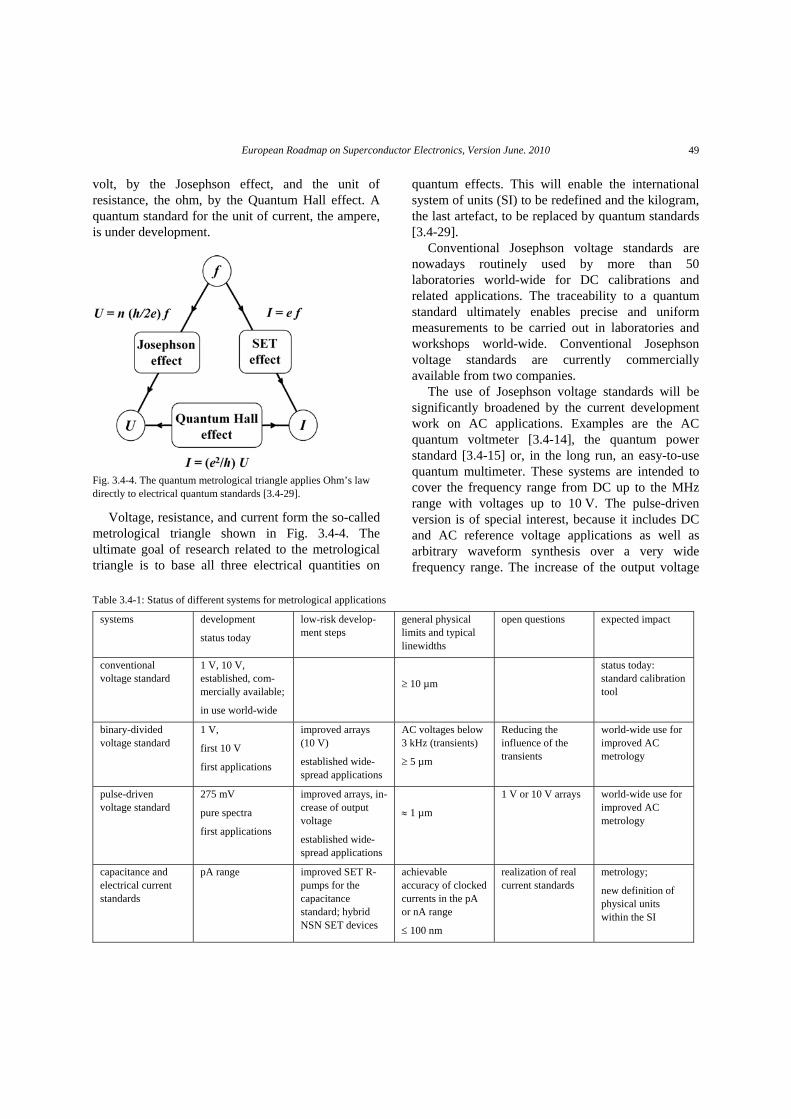
European Roadmap on Superconductor Electronics, Version June. 2010 49
volt, by the Josephson effect, and the unit of resistance, the ohm, by the Quantum Hall effect. A quantum standard for the unit of current, the ampere, is under development.
Voltage, resistance, and current form the so-called metrological triangle shown in Fig. 3.4-4. The ultimate goal of research related to the metrological triangle is to base all three electrical quantities on
quantum effects. This will enable the international system of units (SI) to be redefined and the kilogram, the last artefact, to be replaced by quantum standards [3.4-29].
Conventional Josephson voltage standards are nowadays routinely used by more than 50 laboratories world-wide for DC calibrations and related applications. The traceability to a quantum standard ultimately enables precise and uniform measurements to be carried out in laboratories and workshops world-wide. Conventional Josephson voltage standards are currently commercially available from two companies.
The use of Josephson voltage standards will be significantly broadened by the current development work on AC applications. Examples are the AC quantum voltmeter [3.4-14], the quantum power standard [3.4-15] or, in the long run, an easy-to-use quantum multimeter. These systems are intended to cover the frequency range from DC up to the MHz range with voltages up to 10 V. The pulse-driven version is of special interest, because it includes DC and AC reference voltage applications as well as arbitrary waveform synthesis over a very wide frequency range. The increase of the output voltage
Fig. 3.4-4. The quantum metrological triangle applies Ohm’s law directly to electrical quantum standards [3.4-29].
Table 3.4-1: Status of different systems for metrological applications
open questions expected impact systems development low-risk develop-ment steps
general physical limits and typical linewidths
status today
conventional voltage standard
1 V, 10 V, established, com-mercially available;
status today: standard calibration tool
≥ 10 µm
in use world-wide
world-wide use for improved AC metrology
AC voltages below 3 kHz (transients)
Reducing the influence of the transients
binary-divided voltage standard
1 V, improved arrays (10 V) first 10 V
≥ 5 µm established wide-spread applications
first applications
1 V or 10 V arrays world-wide use for improved AC metrology
pulse-driven voltage standard
275 mV improved arrays, in-crease of output voltage
≈ 1 µm pure spectra
first applications established wide-spread applications
realization of real current standards
metrology; achievable accuracy of clocked currents in the pA or nA range
pA range improved SET R-pumps for the capacitance standard; hybrid NSN SET devices
capacitance and electrical current standards
new definition of physical units within the SI
≤ 100 nm

3. Application of Superconductor Electronics, Fundamental Metrology 50
to levels of 1 V or even 10 V is the main challenge of this development due to the requirement of homo-geneously supplying a large number of Josephson junctions with a complex pulse drive.
A promising alternative for the pulse pattern generator is the use of SE circuits for the pulse drive [3.4-31]. This so-called Quantum Synthesizer was recently investigated and realized in a multi-chip configuration consisting of an RSFQ pattern generator in LTS Nb technology, an amplifier in semiconductor technology, a Josephson junction series array as a quantizer, and a cryo-cooler. Circular shift registers serve as memory devices. A 128-bit circular RSFQ shift register memory for digitizing, memory, and further processing was designed to have signal processing speeds higher than 10 GHz, fabricated and tested [3.4-21].
The first quantum current standards are able to provide quantum currents in the range of a few pA. But even these small reference currents have already been used for calibrating current standards based upon charging capacitors.
Superconductor electronics is playing an important role for fundamental metrology and high-precision measurements as shown in Table 3.4-1. Devices based on superconductivity have resulted in quantum standards, which permit measurements at an accuracy level that can not be reached using room temperature instrumentation. Tab. 3.4-2 shows some expected developments in the field of high-precision measure-ments and their timeline. In particular, improved
Josephson voltage standards for low-frequency AC applications and improvements of capacitance standards are expected within the next 2 years. Goals for the next 5 years are improved pulse-driven voltage standards for output voltages up to 1 V and first real electrical current standards. The quantum multimeter, pulse-driven voltage standards for output voltages up to 10 V, and improved electrical current standards are expected within the next 5 to 10 years.
References
[3.4-1] B.D. Josephson, Phys. Lett. 1 (1962) 251. [3.4-2] J. Niemeyer, J.H. Hinken, and R.L. Kautz, Appl. Phys.
Lett. 45 (1984) 478. [3.4-3] J. Kohlmann, R. Behr, and T. Funck, Meas. Sci. Techn. 14
(2003) 1216. [3.4-4] C.A. Hamilton, Rev. Sci. Instrum. 71 (2000) 3611. [3.4-5] H. Yoshida, IEICE Trans. Electron. E78-C (2000) 20. [3.4-6] G. Wende, M. Schubert, T. May, L. Fritzsch, H.-G. Meyer,
G. Thummes, Y. Kücükkaplan, L.M. Qiu, J. Kohlmann, J. Niemeyer, H. Hofmeister, and J. Scheerer, IEEE Trans. Appl. Supercond. 13 (2003) 915.
[3.4-7] D. Reymann, T. Witt, G. Eklund, H. Pajander, H. Nilsson, R. Behr, T. Funck, and F. Müller, IEEE Trans. Instrum. Meas. 48 (1999) 257.
[3.4-8] A.K. Jain, J.E. Lukens, and J.-S. Tsai, Phys. Rev. Lett. 58 (1987) 1165.
[3.4-9] C.J. Burroughs, S.P. Benz, P.D. Dresselhaus, B.C. Waltrip, T.L. Nelson, Y. Chong, J.M. Williams, D. Henderson, P. Patel, L. Palafox, and R. Behr, IEEE Trans. Instrum. Meas. 56 (2007) 289.
[3.4-10] O. Kieler, R. Behr, F. Müller, H. Schulze, J. Kohlmann, and J. Niemeyer, Physica C 372-376 (2002) 309.
Tab. 3.4-2: Expected developments in the field of high-precision measurements and their timeline.
SE High-Precision Measurement
Basic R&D
Basic R&D
Basic R&D
Basic R&D
Applied R&D
Applied R&D
Applied R&D
Applied R&D
Applied R&D
First Appl.
First Appl.
First Appl.
First Appl.
First Appl.
Mature Appl.
Mature Appl.
Mature Appl.
Mature Appl.
2010 2011 2012 2013 2014 2015 2016 2017 2018 2019 2020
Quantum Multimeter
Electric Current Standards
Capacitance Standards
AC-Josephson Voltage Standard (f<1MHz)
Low -Frequency AC Josephson VoltageStandard

European Roadmap on Superconductor Electronics, Version June. 2010 51
[3.4-11] F. Müller, R. Behr, L. Palafox, J. Kohlmann, R. Wendisch, and I. Krasnopolin, IEEE Trans. Appl. Supercond. 17 (2007) 649.
[3.4-12] F. Mueller, R. Behr, T. Weimann, L. Palafox, D. Olaya, P. D. Dresselhaus, and S. P. Benz, IEEE Trans. Appl. Supercond. 19 (2009) 981.
[3.4-13] M. Ishizaki, H. Yamamori, A. Shoji, P. Dresselhaus, and S. Benz, IEEE Trans. Instrum. Meas. 54 (2005) 620.
[3.4-14] R. Behr, L. Palafox, G. Ramm, H. Moser, and J. Melcher, IEEE Trans. Instrum. Meas. 56 (2007) 235.
[3.4-15] L. Palafox, G. Ramm, R. Behr, W.G.K. Ihlenfeld, and H. Moser, IEEE Trans. Instrum. Meas. 56 (2007) 534.
[3.4-16] S.P. Benz and C.A. Hamilton, Appl. Phys. Lett. 68 (1996) 3171.
[3.4-17] S.P. Benz, C.A. Hamilton, C.J. Burroughs, and T.E. Harvey, IEEE Trans. Instrum. Meas. 48 (1999) 266.
[3.4-18] J.M. Williams, T.J.B.M. Janssen, L. Palafox, D.A. Humphreys, R. Behr, J. Kohlmann, and F. Müller, Supercond. Sci. Technol. 17 (2004) 815.
[3.4-19] H.E. van den Brom, E. Houtzager, B.E.R. Brinkmeier, and O.A. Chevtchenko, IEEE Trans. Instrum. Meas. 57 (2008) 428.
[3.4-20] O.F. Kieler, R. Iuzzolino, and J. Kohlmann, IEEE Trans. Appl. Supercond. 19 (2009) 230.
[3.4-21] Final Report of BMBF project Quantum Synthesizer: F.-Im. Buchholz, J. Kohlmann, M. Khabipov, C.M. Brandt, D. Hagedorn, D. Balashov, F. Maibaum, E. Tolkacheva, and J.
Niemeyer, “Integrierte digitale supraleitende Logik-schaltungen für den Quanten-Synthesizer - Bericht über das BMBF-Vorhaben 13N8412“, PTB-Bericht PTB-E-93, Braunschweig 2006, ISBN 3-86509-619-0 (in German).
[3.4-22] S.P. Benz, P.D. Dresselhaus, A. Rüfenacht, N.F. Bergren, J.P. Kinard, and R.P. Landim, IEEE Trans. Instrum. Meas. 58 (2009) 838.
[3.4-23] T.E. Lipe, J.R. Kinard, Yi-hua Tang, S.P. Benz, C.J. Burrroughs, and P.D. Dresselhaus, Metrologia 45 (2008) 275.
[3.4-24] S.P. Benz, J. Qu, H. Rogalla, D.R. White, P.D. Dresselhaus, W.L. Tew, and S.W. Nam, IEEE Trans. Instrum. Meas. 58 (2009), 884.
[3.4-25] S.V. Lotkhov, S.A. Bogoslovsky, A.B. Zorin, and J. Niemeyer, Appl. Phys. Lett. 78 (2001) 946.
[3.4-26] J.P. Pekola, J.J. Vartiainen, M. Mottonen, O.-P. Saira, M. Meschke, and D.V. Averin, Nature Phys. 4 (2008) 120.
[3.4-27] S. Lotkhov, V.A. Krupenin, and A.B. Zorin, IEEE Trans. Instrum. Meas. 56 (2007) 491.
[3.4-28] J.E. Mooij and Yu.V. Nazarov, Nature Phys. 2 (2006) 169.
[3.4-29] I.M. Mills, P.J. Mohr, T.J. Quinn, B.N. Taylor, and E.R Williams, Metrologia 43 (2006) 227.
[3.4-30] K.K. Likharev and A.B. Zorin, J. Low Temp. Phys. 59 (1985) 347
[3.4-31] M. Khabipov, F.-Im. Buchholz, J. Niemeyer, G. Wende, and H.-G. Meyer, IOP Conf. Ser. 181 (2004) 3459.

3. Application of Superconductor Electronics, Artificial Atoms 52
3.5. Artificial Atoms
Quantum computing went from a purely theoretical concept to successful building of few-qubit prototypes in rather short time. Wild hopes and profound skepticism often went hand-in-hand. A number of elegant proposals, feasible in principle, have run into technological difficulties (e.g., The Kane quantum computer [3.5-1]). Quantum error correction ensures that quantum computation is possible in principle, but it requires a large overhead in terms of additional qubits and operations. The scale of this overhead is extremely sensitive to uncontrollable assumptions about the character of decoherence in the system, and even in the best-case scenario, a practical realization of even small demonstration prototypes is not yet feasible [3.5-2]. On the bright side, one- and two-qubit quantum gates were successfully performed in solid-state based systems, in particular, in superconducting structures [3.5-3]. Superconducting structures are attractive due to their intrinsic protection against decoherence, compared to normal structures of comparable size, well-understood physics, and well developed design, fabrication and measurement techniques [3.5-4].
Successful realization of superconducting qubits, with a path to scalability and realization of quantum error correction (therefore “standard” gate-based quantum computing) requires substantial improvement of the qubit coherence times. On the one hand, intrinsic imperfections of the materials
used for qubit fabrication induce decoherence. That is why the development of a new fabrication process based on low noise, high quality materials becomes one of the central themes for further research. On the other hand, the read-out of the quantum state by means of classical electronics is the second source of decoherence. This feedback should be minimized by choosing a proper detector. However, even with currently available techniques, there are less demanding approaches to quantum computing: so called adiabatic quantum computing [3.5-5] and approximate adiabatic quantum computing [3.5-6]. In these approaches, the system always remains in or close to the ground state, and its precise time evolution is not important (unlike gate-based quantum computing, which demands precise time-domain control of each qubit’s operation). We therefore suggest that the research should be conducted in the direction of study decoherence mechanisms in the superconducting structures, improvement their measurements procedure as well as investigation multuqubit circuits and their operation in adiabatic or quasiadiabatic regime. Such quantum-coherent structures may be also useful outside the field of quantum computing (e.g., as quantum metamaterials [3.5-7]). The experience which European research institutions have in the theory of such structures, their design, fabrication and manipulation, ensures a high probability of success.
Table 3.5-1: Status of Artificial Atoms
development status today
low risk development steps
general physical limits
open questions expected impact
new generation of the information processing devices
Existence of fundamental limits to scaling up quantum coherent circuits
no fundamental limits to scaling up exist in accepted theory; none were so far found on experiment
materials issues to improve qubits characteristics
demonstrated physical principle
Quantum-classical transition
new quantum coherent metamaterials
measurement issues to minimize feedback from a detector to qubit
Limits of validity of quantum mechanics
control issues to minimize feedback from control circuits/need in control circuits
Corrections to quantum mechanics

European Roadmap on Superconductor Electronics, Version June 2010 53
Reference
[3.5-1] B.E. Kane, Nature 393, 1331 (1998). [3.5-2] D. Aharonov, A. Kitaev, and J. Preskill, Phys. Rev. Lett.
96, 050504 (2006). [3.5-3] M. Steffen et al., Science 313, 1423 (2006); A.O. Niskanen
et al., Science 316, 723 (2007) ; J. H. Plantenberg, P. C. de Groot, C. J. P. M. Harmans and J. E. Mooij, Nature 447, 836 (2007).
[3.5-4] A.M. Zagoskin and A. Blais, Physics in Canada 63, No.4, 215 (2007); M.R. Geller et al., in: M.E. Flatte and I. Tifrea (eds.), Manipulating Quantum Coherence in Solid State Systems, NATO Science Series II, Springer, Dordrecht (2007); F.K. Wilhelm et al., ibid.; G. Wendin and V.S. Shumeiko, in M. Rieth and W. Schommers (eds.), Handbook of Theoretical and Computational Nanotechnology, vol.3, American Scientific Publishers (2006); J.Q. You and F. Nori, Physics Today, No.11, 42 (2005).
[3.5-5] E. Farhi et al., Science 292, 472 (2001); A. Mizel, D.A. Lidar, and M. Mitchell, Phys. Rev. Lett. 99, 070502 (2007).
[3.5-6] A.M. Zagoskin, S. Savel’ev, and F. Nori, Phys. Rev. Lett. 98, 120503 (2007).
[3.5-7] A.L. Rakhmanov, A.M. Zagoskin, S. Savel'ev, and F. Nori, Phys. Rev. B 77, 144507 (2008).
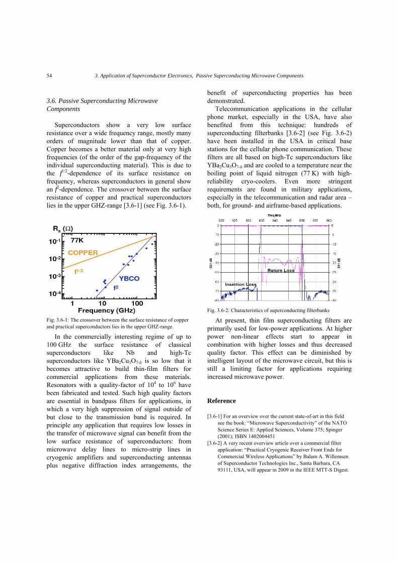
3. Application of Superconductor Electronics, Passive Superconducting Microwave Components 54
3.6. Passive Superconducting Microwave Components
Superconductors show a very low surface resistance over a wide frequency range, mostly many orders of magnitude lower than that of copper. Copper becomes a better material only at very high frequencies (of the order of the gap-frequency of the individual superconducting material). This is due to the f1/2-dependence of its surface resistance on frequency, whereas superconductors in general show an f2-dependence. The crossover between the surface resistance of copper and practical superconductors lies in the upper GHZ-range [3.6-1] (see Fig. 3.6-1).
In the commercially interesting regime of up to 100 GHz the surface resistance of classical superconductors like Nb and high-Tc superconductors like YBa2Cu3O7-δ is so low that it becomes attractive to build thin-film filters for commercial applications from these materials. Resonators with a quality-factor of 104 to 106 have been fabricated and tested. Such high quality factors are essential in bandpass filters for applications, in which a very high suppression of signal outside of but close to the transmission band is required. In principle any application that requires low losses in the transfer of microwave signal can benefit from the low surface resistance of superconductors: from microwave delay lines to micro-strip lines in cryogenic amplifiers and superconducting antennas plus negative diffraction index arrangements, the
benefit of superconducting properties has been demonstrated.
Telecommunication applications in the cellular phone market, especially in the USA, have also benefited from this technique: hundreds of superconducting filterbanks [3.6-2] (see Fig. 3.6-2) have been installed in the USA in critical base stations for the cellular phone communication. These filters are all based on high-Tc superconductors like YBa2Cu3O7-δ and are cooled to a temperature near the boiling point of liquid nitrogen (77 K) with high-reliability cryo-coolers. Even more stringent requirements are found in military applications, especially in the telecommunication and radar area – both, for ground- and airframe-based applications.
Fig. 3.6-2: Characteristics of superconducting filterbanks
At present, thin film superconducting filters are primarily used for low-power applications. At higher power non-linear effects start to appear in combination with higher losses and thus decreased quality factor. This effect can be diminished by intelligent layout of the microwave circuit, but this is still a limiting factor for applications requiring increased microwave power.
Fig. 3.6-1: The crossover between the surface resistance of copper and practical superconductors lies in the upper GHZ-range.
Reference
[3.6-1] For an overview over the current state-of-art in this field see the book: “Microwave Superconductivity” of the NATO Science Series E: Applied Sciences, Volume 375; Spinger (2001); ISBN 1402004451
[3.6-2] A very recent overview article over a commercial filter application: “Practical Cryogenic Receiver Front Ends for Commercial Wireless Applications” by Balam A. Willemsen of Superconductor Technologies Inc., Santa Barbara, CA 93111, USA, will appear in 2009 in the IEEE MTT-S Digest.

European Roadmap on Superconductor Electronics, Version June 2010 55
4. Materials and Fabrication Technology for Superconductor Electronics
Since the discovery of the Josephson Effect in 1962, the application of superconductivity to electronics has been a challenging field of work for both physicists and engineers.
The Nb-AlOX-Nb junction process was invented in 1983 [4-1] and has since then become the principal technology for superconductor electronics on the liquid helium level (4.2 K). Digital electronics achieved relevance when the Rapid Single Flux Quantum (RSFQ) logic, first reported in 1985, became popular in the late 1980’s [4-3]. Public funding in the 1990’s, in particular in Japan and in the U.S., has enabled rapid progress in this field and as a result several RSFQ IC foundries were established worldwide and are operating to this day. In Japan there are fabrication facilities at ISTEC/SRL, in the U.S. at HYPRES, NIST, and TRW, and in Europe at IPHT [4-4] and PTB [4-5], both in Germany, at VTT in Finland [4-6], [4-7], and at CNR in Italy. Linewidth reduction and phase engineering are currently the major fields of research for Josephson junction.
On the system level, cooling is a major issue. Therefore, other materials were considered that allow higher operation temperatures. Early developments in this direction are based on Josephson junctions of the type NbN-MgO-NbN with operation temperatures in the range of 10 K. High expectations were raised when in 1986 high temperature superconductivity (HTS) was discovered. For electronic application YBCO became the standard material for cooling on the liquid nitrogen level (77 K). The research activities for YBCO digital circuits were mainly focused on freely positionable ramp-type Josephson junctions. Since in 2001 another superconductor, MgB2 (magnesium diboride) was discovered this material is under discussion for superconductor electronics with an operation temperature of 20 K.
Superconducting radiation detectors are based on either application-specifically designed Josephson junctions (e.g. STJ) or single superconducting thin films (e.g. TES).
4.1. Nb Josephson Junctions and Circuits
Compared to the other superconductor circuits and sensors, digital RSFQ logic has the fabrication process with the highest complexity. Currently, the niobium-based Nb-AlOX-Nb junction technology is the only candidate for VLSI superconductor digital electronics circuits.
The Nb-AlOX-Nb Josephson junction is a superconductor-insulator-superconductor (SIS) junction. The electronic behaviour of the unshunted (underdamped) SIS junction is a hysteretic function. The shunted (damped) SIS junction is a parallel connection with a resistor (shunt). The nonhysteretic function of such a shunted SIS junction is necessary for the RSFQ logic. Another possibility to avoid the hysteresis is the integration of a resistive barrier into the Josephson junction. Such established junction types are superconductor-normal metal-superconductor (SNS) or superconductor-insulator-normal metal-insulator-superconductor (SINIS). Their implementation in digital circuits is in discussion.
Basically, the Nb-AlOX-Nb standard technology utilizes a sandwich structure of successively processed superconducting Nb and insulating SiO2 layers. The Nb layers are used to wire the Josephson junctions and to shield them from magnetic fields. The number of stacked superconducting layers differs in the various foundry processes. For resistors, a normal metal layer is included.
The Josephson junctions are integrated in this process as the so-called trilayer, which is a sequence of the layers Nb-Al-AlOX-Nb deposited in situ in order to obtain clean interfaces. AlOX acts as the tunnel barrier. The critical current density jC of the Josephson junction is a major issue for both fabrication technology and application. This parameter depends exponentially on the thickness of the AlOX tunnelling barrier and is set during fabrication process by the oxygen exposure [4-9] (see Fig. 4-1).
The barrier is quite thin, typically only a few nanometres. It is technologically challenging to obtain perfectly leakage-free AlOX layers. The standard value ranges of jC are for digital electronics 1 kA/cm2, for SQUID sensors 100 A/cm2, and for

4. Materials and Fabrication Technology for Superconductor Electronics 56
metrology circuitry 10 A/cm2. For some applications at ultra-low temperatures even lower critical current densities are considered.
As described elsewhere, the intrinsic switching
time of superconductor electronics is very short, of the order of a few picoseconds. In addition, their power dissipation is very low, below one microwatt per junction, which is a thousand times less than for CMOS. The switching time is determined by the gap voltage Vg (which is a material parameter) of 1.4 mV and jC (which is a process parameter). To benefit from the unique features of superconductor electronics the fabrication technology has to be modified to increase jC as the junction sizes decrease.
The shrinkpath for LSI or VLSI superconductor electronic circuitry is governed by two scaling rules which are shown in Fig. 4-2 [4-10]. The clock rate of complex circuits can be increased with the square root of critical current density while the junction size has to be reduced by the reciprocal of the same square root. Apart from the fact that the thermal budget would not permit highly integrated semiconductor circuits to operate at several tens of gigahertz clock rate, it should be noted here that superconductor circuits can achieve such clock rates using a lithography resolution of a few microns.
Fig. 4-2: Shrink path for superconductor electronics. Scaling the junction size down to 0.3 µm the clock speed of integrated circuits can be increased well-above 100 GHz.
A 100 kA/cm2 sub micrometer Josephson junction
process would give access to complex digital circuitries with clock rates far above one hundred gigahertz. More details about this exciting possibility are shown in Tab. 4-1.
Currently, the most important application of superconductor electronics is the SQUID sensor. The SQUID fabrication can be considered as simplified variant of the RSFQ process.
Tab. 4-1: Basic figures of merit for niobium-trilayer RSFQ circuits for different minimum feature sizes as described in [4-10].
Josephson junction size
Integrated circuit density
Integra-tion Level
RSFQ pulse width
Maximum Clock rate
Minimum power dissipation
[μm] [cells per cm²]
[ps] [GHz] [μW per cell]
3.5 10,000 LSI 4 10-40 0.03
1.5 30,000 VLSI 2 40-80 0.06
0.8 100,000 ULSI 1 70-130 0.1
0.4 1,000,000 SLSI 0.8(?) 100-200(?) 0.15(?)
Other Nb-based, junction types such as
superconductor-normal metal-superconductor (SNS) or superconductor-insulator-normal metal-insulator-superconductor (SINIS) are discussed for digital
Fig. 4-1: Critical current density as a function of oxygen exposition; ultra-violet light-assisted oxidation allows to reach very low values of the critical current density (triangles).
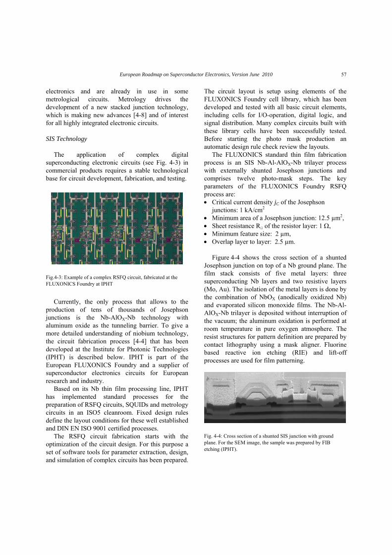
European Roadmap on Superconductor Electronics, Version June 2010 57
electronics and are already in use in some metrological circuits. Metrology drives the development of a new stacked junction technology, which is making new advances [4-8] and of interest for all highly integrated electronic circuits.
SIS Technology The application of complex digital
superconducting electronic circuits (see Fig. 4-3) in commercial products requires a stable technological base for circuit development, fabrication, and testing.
Currently, the only process that allows to the
production of tens of thousands of Josephson junctions is the Nb-AlOX-Nb technology with aluminum oxide as the tunneling barrier. To give a more detailed understanding of niobium technology, the circuit fabrication process [4-4] that has been developed at the Institute for Photonic Technologies (IPHT) is described below. IPHT is part of the European FLUXONICS Foundry and a supplier of superconductor electronics circuits for European research and industry.
Based on its Nb thin film processing line, IPHT has implemented standard processes for the preparation of RSFQ circuits, SQUIDs and metrology circuits in an ISO5 cleanroom. Fixed design rules define the layout conditions for these well established and DIN EN ISO 9001 certified processes.
The RSFQ circuit fabrication starts with the optimization of the circuit design. For this purpose a set of software tools for parameter extraction, design, and simulation of complex circuits has been prepared.
The circuit layout is setup using elements of the FLUXONICS Foundry cell library, which has been developed and tested with all basic circuit elements, including cells for I/O-operation, digital logic, and signal distribution. Many complex circuits built with these library cells have been successfully tested. Before starting the photo mask production an automatic design rule check review the layouts.
The FLUXONICS standard thin film fabrication process is an SIS Nb-Al-AlOX-Nb trilayer process with externally shunted Josephson junctions and comprises twelve photo-mask steps. The key parameters of the FLUXONICS Foundry RSFQ process are: • Critical current density jC of the Josephson
junctions: 1 kA/cm2 • Minimum area of a Josephson junction: 12.5 µm2, • Sheet resistance R of the resistor layer: 1 Ω, • Minimum feature size: 2 µm, • Overlap layer to layer: 2.5 µm.
Figure 4-4 shows the cross section of a shunted Josephson junction on top of a Nb ground plane. The film stack consists of five metal layers: three superconducting Nb layers and two resistive layers (Mo, Au). The isolation of the metal layers is done by the combination of NbOX (anodically oxidized Nb) and evaporated silicon monoxide films. The Nb-Al-AlOX-Nb trilayer is deposited without interruption of the vacuum; the aluminum oxidation is performed at room temperature in pure oxygen atmosphere. The resist structures for pattern definition are prepared by contact lithography using a mask aligner. Fluorine based reactive ion etching (RIE) and lift-off processes are used for film patterning.
Fig.4-3: Example of a complex RSFQ circuit, fabricated at the FLUXONICS Foundry at IPHT
Fig. 4-4: Cross section of a shunted SIS junction with ground plane. For the SEM image, the sample was prepared by FIB etching (IPHT).

4. Materials and Fabrication Technology for Superconductor Electronics 58
The function and thickness of the different layers are shown in Tab. 4-2.
SINIS and SNS Technology Another application of superconductor electronics
is the quantum Josephson voltage standard. For the more recent programmable Josephson voltage standards arrays of Josephson junctions with intrinsic damping are employed. Two different junction technologies are currently well established: SINIS junctions for operation about 70 GHz and SNS junctions for operation about 15 GHz. A new metrology application is the arbitrary waveform synthesizers based on pulse-driven SNS junction arrays.
A particular requirement for all kinds of Josephson voltage standard arrays is the uniform supply of all junctions with microwave power. The junctions are therefore integrated into suitable high-frequency transmission lines. Different types of lines like low-impedance microstrip lines [4-11], [4-12], [4-13], coplanar waveguide transmission lines (CPW) [4-12], or coplanar striplines (CPS) [4-14] are used mainly depending on the required frequency range. Typical thicknesses of the layers are compiled in Tab. 4-3. The metallic layers are deposited by sputtering, the dielectrics by sputtering, CVD or
PECVD. Patterning is done by optical photolitho-graphy or electron-beam lithography and fluorine based dry etching processes.
SINIS junctions (see Fig. 4-5) are very sensitive to
process parameter stability due to the extremely thin oxide barriers. Therefore, a few junctions of the arrays are often accidentally shorted. The fabrication of arrays containing a large number of junctions is challenging.
The use of SNS junctions would overcome these difficulties as these are more robust. Several different materials for the normal metal in these junctions have been investigated, i.e. PdAu, MoSi2, and NbxSi1-x [4-15] of which the latter is very promising. The first 10-V SNS arrays were successfully fabricated without single junction failures [4-16].
To reduce the substrate area and to increase the
integration density, stacks of up to 9 junctions for
Tab. 4-2: Functionality and thickness of the different layers of the FLUXONICS Foundry RSFQ process.
Name Function Material Thickness (nm)
M0 Ground plane Nb 250
I0A Isolation Nb2O5
SiO
50
100
I0B Isolation SiO 100
M1 Wiring 1 Nb 250
T1 Trilayer Nb/Al-AlOX/Nb 60/12/30
I1A Isolation Nb2O5 70
I1B Isolation SiO 180
R1 Shunt Mo 80
I2 Isolation SiO 170
M2 Wiring 2 Nb 350
R2 Bond Au 45
Table 4-3: Typical thicknesses of the different layers for voltage tandard applications (cf. [4-11, 4-12]). s base electrode 150 nm – 200 nm
Aluminium layer (SIS) 10 nm (1 nm – 2 nm Al2O3)
Aluminium layer (SINIS) 3 x 10 nm (< 1 nm each Al2O3)
Normal metal (SNS) 10 nm – 30 nm
top electrode 80 nm – 200 nm
insulating layer 250 nm – 350 nm
wiring layer 300 nm – 600 nm
dielectric layer for microstrip lines
1 µm – 2 µm
ground plane 150 nm – 300 nm
Fig. 4-5: Schematic cross section of a low-impedance microstrip line.with SINIS junctions.

European Roadmap on Superconductor Electronics, Version June 2010 59
small series arrays [4-17] have been fabricated. Junction sizes about 1 µm typically are used for arbitrary waveform synthesizers based on pulse-driven junction arrays.
Typical parameters of SINIS [4-18] and SNS [4-19], [4-20] series arrays are summarized in Table 4-4.
Methods of achieving nanometre Josephson Junction size
The necessity for reducing Josephson junction size
to submicron dimensions arises from the need to increase clock frequency, reduce capacitances and increase integration density for superconducting digital electronic circuits. It is also important for special applications in metrology, e.g. qubits or single charge tunnelling (SET) devices.
In RSFQ circuits the critical current IC is fixed by design considerations. Therefore an increase of the critical current density jC in order to increase the clock frequency means reduction of junction size and that allows higher integration densities. So e.g. at a current density of 100 kA/cm2 the junction area has to be in the range of 0.1 um2 compared to 10um2 at 1 kA/cm2. The nonhysteretic I-V characteristic of the SIS-type junctions is obtained by external shunting, but these shunt resistors consume chip area. In the case of very high jC (>100 kA/cm2) the junctions become nonhysteretic without the need of external shunt resistors [4-63], [4-64]. Thus such junctions seem to give ideal device performance for digital circuit applications. However there are strong
technological problems with process reproducibility and stability which arise in the preparation of the extremely thin (in the range of one monolayer) oxide tunnelling barriers.
SINIS or SNS junctions are intrinsically shunted. SNS junctions might be an alternative to high jC SIS-junctions. They allow high current densities at relative thick N-layers, but suffer from lower ICRN products compared to SIS junctions. With SINIS-junctions only low current densities can be obtained, which are outside the range of interest for digital superconducting circuits.
The first submicron SIS-type tunnel junctions were prepared by an aluminium shadow evaporation technique [4-65], [4-66], which currently has a renaissance in the preparation of qubit and SET devices [4-67]. After the invention of the Nb trilayer process [4-1] several modified processes were developed in order to fabricate Josephson junctions with submicron tunneling areas [4-68]-[4-73]. The problem of reliable junction sidewall isolation becomes dominant at lateral junction dimensions smaller than 1 µm. The introduction of the chemical-mechanical polishing (CMP) technique [4-73] was an important step to solve this isolation problem and to strongly improve the quality of wiring connections by minimizing the step heights in circuits with a large number of layers.
As example a process, developed for the
fabrication of pulse-driven SNS series arrays, combines e-beam lithography and chemical-mechanical polishing (CMP), cf. Fig. 4-6 allows the fabrication of sub-µm junctions [4-18], [4-20].
Fig. 4-6: Schematic cross section of SNS junctions prepared by multilayer Nb technology using CMP
The total capacitance of the Josephson junctions depends not only on the junction area and barrier material, but also on the immediate surroundings of the junction, which adds parasitic capacitance. Especially in the case of extremely small junction areas this parasitic capacitance can dominate the total capacitance. Therefore the cross-type junction design
Table 4-4: Parameters of SINIS and SNS junctions for programmable and pulse-driven Josephson voltage standards.
SINIS
programmable
SNS
programmable
SNS
pulse-driven
number of junctions
8,192 (1 V), 69,632 (10 V)
8,192 (1 V), 69,632 (10 V)
1,000 – 12,000
length of junctions
10 µm-20 µm 6 µm 0.7 µm-2.5 µm
width of junctions
30 µm-50 µm 20 µm 0.7µm-2.5 µm
critical current density
100 A/cm2 – 500 A/cm2
2.5 kA/cm2 50 kA/cm2 – 100 kA/cm2
Nb
NbSiO2
Substrate

4. Materials and Fabrication Technology for Superconductor Electronics 60
[4-71], [4-72] is of particular interest for the fabrication of circuits with extremely low parasitic junction capacitances [4-74] in addition to the advantage of better lithographical junction area definition.
4.2. Complementary Superconductive Materials
For many applications, Nb based fabrication technologies are a natural choice due to their ability to construct complex circuits containing large numbers of junctions with a high degree of reproducibility. However some alternative materials like NbN, YBaCuO7-x (YBCO) and MgBB2 do provide capabilities not available with the basic Nb based process and the fabrication of Josephson devices can also provide a deeper understanding of superconductivity itself.
NbN Josephson Junctions and Circuits NbN films have attracted significant attention for
application in superconductive electronics because of their attractive material parameters like the high critical temperature Tc of about 15 K and the large gap voltage Vg of 5 mV. These parameters make NbN very promising for higher operation temperatures and high frequency high-speed applications in superconducting electronic devices. However NbN has a larger magnetic penetration depth and a shorter superconducting coherence length than niobium [4-21], [4-22], [4-23], [4-24] (cf. Tab. 4-5).
Tab. 4-5: Comparison of characteristic material parameters of NbN and Nb films.
Parameter NbN Nb
polycrystalline epitaxial polycryst.
Tc / K 12..15 15.4…17.8 9.2
2Δ /mV 5 5.0…5.8 2.8…3.2
λ / nm 300…600 90…100 85
ξ / nm 3…5 7 35 These properties are undesirable for electronics
applications because of increasing parasitic inductances and decreasing quality of all-NbN
Josephson junctions caused by the low coherence length.
All-NbN technologies ([4-25], [4-26], [4-27], [4-28]) were developed for the preparation of Josephson junctions and complex superconducting logic circuits, pushed especially by the expectations for high operation temperatures with decreased cooling demands. There are no substantial differences between the NbN- and Nb-processes concerning the types of Josephson junctions (SIS, SNS, SINIS), the structure sizes or the number of layers in complex circuits. But the parameter spreads and functional complexity of all-NbN integrated circuit technologies has not reached the quality and yield level of established Nb technologies. This may be caused by the fabrication process of so-called artificial type [4-29] tunneling barriers, which are prepared by direct deposition of the barrier material (MgO, AlN, NbNx,…). Any deviation in film thickness or homogeneity strongly influences the wafer to wafer or chip to chip spread of junction current density. Tunnel barrier preparation is a technological challenge, especially for the case of high current densities, which are required for high clock frequencies in integrated digital circuits. E.g. the thickness of the directly deposited MgO barrier for jc = 50 kA/cm2 in NbN/MgO/NbN junctions is only 0.4 nm! [4.27]. Further, the NbN films are deposited usually by reactive processes which are more sensitive to parameter deviations. This influences the film stoichiometry and parameter reproducibility. The deposition of single-crystalline NbN films is a possible method to minimize the drawbacks of the values of the penetration depth and coherence length [4-21], [4-22]. Epitaxial NbN films can be deposited at high substrate temperatures or by using MgO single crystal substrates or MgO buffer layers on silicon substrates for room temperature deposition. High substrate temperatures cannot be used in multilayer processes for superconducting electronic circuits because of degradation effects.
Presently, high quality NbN films are used for high frequency detector applications. NbN tunnel junctions are operating in SIS-mixers in the sub-millimeter wavelength range because of their high gap frequency of 1.4 THz [4-30], [4-31], [4-32]. For superconducting single photon detectors epitaxial NbN films deposited onto MgO substrates are of

European Roadmap on Superconductor Electronics, Version June 2010 61
growing interest [4-33], [4-34]. They show high quantum efficiencies at fast response time at moderate cooling needs of 4 K. Despite the particular technological difficulties of the all-NbN process for large scale integration digital circuits, NbN has the potential to offer improved clock frequency and bit error rates. If the technological requirements and the related practical restrictions are under control, then all-NbN electronic circuits could advance beyond the limitations of Nb devices.
Table 4-6: Pros and cons for an all-NbN fabrication process for highly integrated superconducting digital electronic circuits compared to all-Nb technologies
Pro Con
higher Tc:
higher operating temperature
higher penetration depth: higher parasitic inductances
higher gap energy:
lower bit error rate
lower coherence length:
lower quality and reproducibility of JJ
higher gap frequency:
higher clock frequencies
lower Hc:
higher sensitivity to flux trapping
lower development status of fabrication technologies for highly integrated circuits
MgB2 devices
For superconductor electronics, the main interest in MgBB2 is the 40 K transition temperature. In addition, there have been a number of proposals for bolometric detectors [4-36]. Production of devices from this material is challenging both at the level of thin film deposition and junction fabrication. Mg and B have very different vapour pressures, both elements oxidize easily and at temperatures above 300 °C, the sticking coefficient of Mg is very low. There is much work still to do in the development of junction technologies suitable for this material, but there has been some success in the production of tunnel junctions [4-38] and with the use of ion beams to fabricate junctions [4-39], [4-40], [4-41]. In particular, bridges created using Focused Ion beam systems have been used to construct SQUIDs and magnetometers by damaging the material [4-40] or
making nanoconstrictions [4-41]. Excellent performance has also been achieved using MgB2B bridges in mixers for THz applications [4-36]
YBCO devices. YBCO is a ceramic oxide material and therefore
the high quality thin films needed for electronics applications can only be fabricated by epitaxial growth on well lattice matched substrates. This is achieved using a number of processes including reactive co-evaporation, sputtering and pulsed laser deposition [4-42].
Josephson junctions can be fabricated using all of these techniques and whilst there have been a number of prototype devices, the two most successful types are based upon artificial grain boundaries induced in the oxide thin film or multilayer junctions fabricated on sloped (ramped) edges etched into a YBCO base electrode. These technologies and others have been used to fabricate SQUIDs [4-43] and digital circuits [4-44], [4-45] with operating at temperatures well above those at which Nb based devices operate.
Devices based on intrinsic π− phase shift junctions
The effect of the π phase shift on a superconducting loop is shown in Fig. 4-7 [4-50]. Here we see that for a SQUID with junctions directed at right angles, the critical current is a minimum when no flux is applied, whereas, for a device with the junctions parallel to one another, the usual behaviour is observed. In particular loops which spontaneously generate flux were incorporated in a toggle flip flop as memory storage elements [4-51]. This eliminated the need to bias part of the circuit into a half flux quantum state and increases the tolerance of the circuit to variations in device parameters. In the area of quantum computing, there have been a number of proposals which employ π junctions or the effect of the vanishing of the critical current at the boundary between 0 and π behavior [4-52] [4-53].

4. Materials and Fabrication Technology for Superconductor Electronics 62
Fig. 4-7. Upper part: π SQUID. Lower part 0 SQUID
The use of YBCO as a superconductor allows one
to construct devices with built in π phase shifts and hence superconducting loops which spontaneously generate fractional flux quanta. These devices rely on the dx2-y2 pairing of the YBCO and Josephson devices based on artificial grain boundaries provided some of the earliest definitive evidence of this [4-46], [4-47]. Two techniques have been developed for fabricating devices which make use of the YBCO pairing state. The Twente ramp junction process [4-48] and the Naples/Chalmers process [4-49].
The π phase shifts can also be induced in superconducting loops by inserting a thin ferromagnetic layer next to the oxide barrier of a Nb tunnel junction or using a SFS superconductor-ferromagnet-superconductor junction. When the ferromagnet is placed in contact with the superconductor, a superconducting order parameter is induced, just as it is with a non magnetic metal, however not only does the magnitude of this order parameter decay with distance from the interface, it also oscillates. Hence for ferromagnet layers thicker than a critical value, the order parameter at the free
surface has the opposite sign and is π out of phase with the order parameter in the superconductor. This enables one to construct a π junction.
Fig. 4-8 Critical current versus magnetic field for a 0-p junction
This has been demonstrated with both strong ferromagnets such as Co [4-54] and alloy ferromagnets such as PdNi [4-55]. Weides et al [4-56] confirmed the π phase shift above the critical ferromagnet thickness, by fabricating a junction with two different thicknesses of NiCu in side by side in the barrier. The critical current of this device was small in zero applied magnetic fields and increased to a maximum before decreasing again for both positive and negative fields. (See Fig. 4-8). Ferromagnetic layers can also be used to construct a range of novel devices. One example is the use of a pseudo spin valve between Nb electrodes to give a junction with a controllable critical current [4-57].
4.3. Radiation Detector Technology
New applications of superconducting technology in areas like sub-millimeter astronomy, security screening and x-ray microanalysis are advancing rapidly. The need to detect weak photonic signals and

European Roadmap on Superconductor Electronics, Version June 2010 63
even single photons has given considerable stimulus to the development of very sensitive instruments. Various types of superconductive radiation detectors like micro calorimeters, transition edge sensors (TES), superconducting tunnel junctions (STJ), and superconducting single photon detectors (SSPD) were developed in the past. Their fabrication technology, functionality, and application fields are described elsewhere.
In contrast to superconductive electronic circuits, where a wide variety of functionality can be achieved within a single technology by a combination of only a few basic elements such as Josephson junctions, inductances, capacitors, and resistors, radiation detectors rely on application-specific fabrication technologies. Depending on the wavelength and energy of radiation detectors, either very special material properties of superconducting thin films or particular physical properties of Josephson junctions are exploited. Because of this great variety there exists no general detector fabrication technology, but a lot of demanding tasks in terms of thin film preparation for such detectors in combination with advanced micro- and nanomechanical fabrication techniques are required.
For the next couple of years detector applications will focus on complete imaging systems. This requires large focal plane arrays of radiation detectors with more than 1,000 pixels. The further implementation of detector technologies must follow up this development. Aside from the improvement of the single detector parameters, the reproducibility of the fabrication processes is a major issue. Moreover, large arrays require on-chip integration of electronic signal processing capabilities as well as reliable nanomechanical processes on wafer scale. The challenge for the future will be the implementation of detector technologies together with the fabrication of the sensors, which combines superconductive electronic circuits with nanomechanical functional components.
4.4. Status and Outlook
Currently, the niobium-based SIS junction technology is the only candidate for LSI superconductor electronics circuits with the potential to be further developed to the very large scale
integration (VLSI) level necessary for practical applications.
Apart from their useful physical properties SNS and SINIS junctions are so-called intrinsically shunted junctions and need no extra shunt resistors to be processed. This simplification of technology is of great importance from a fabrication point of view. However, more research effort is needed to make them ready for use, especially for digital circuitry. Robust SNS technologies might be an important alternative to the SIS technology for further reduction of the line width to values smaller than 1 µm.
So far, all the efforts to qualify superconductors with higher critical temperatures for electronics applications did not fully succeed as operating circuits on MSI level could not be demonstrated. The reason for this situation is the material itself. The conventional superconductors such as niobium and aluminum are simple stable metals with a superconducting coherence length of about 80 nm. They are easy to process using thin film deposition and patterning methods, whereas the other above mentioned materials are more complex and more difficult to work with. YBCO for instance is a ceramic material with a comparatively complicated lattice structure and coherence length of only a few nanometres, a value which is close to the reproducibility limit of the YBCO thin film processes. This makes it hard to obtain a reliable fabrication processes for LSI YBCO-based electronic circuits.
A basic overview on the worldwide niobium fabrication facilities for digital superconducting electronic circuits based on niobium SIS junctions and their main process parameters is given in Tab. 4-7. In addition to these facilities, there are worldwide a lot of capabilities for the fabrication of sophisticated superconducting sensors and circuitry. In Europe for example there is. VTT in Finland (SQUID; RSFQ), CNR in Italy (SQUID, SSPD), in Germany PTB (metrological circuits, SQUID, RSFQ), Univ. Karlsruhe (SSPD), IPHT (SQUID, RSFQ, TES, STJ).
Although there are some attempts to obtain higher current density processes for digital circuits, currently most of these containing several thousand Josephson junctions are fabricated by means of the standard 1 kA/cm2 process.

4. Materials and Fabrication Technology for Superconductor Electronics 64
On the present-day technological level digital circuits with up to 10,000 Josephson junctions per chip can be fabricated with a junction failure rate of about 0.01 % at the standard value for the critical current density of 1 kA/cm
Tab. 4-7: Manufacturing facilities for niobium-based digital superconducting electronic circuits on costumer request.
Japan USA EU
Institution ISTEC/SRL Hypres IPHT 2. For the less complex technology of metrology circuits the latter holds even up to 70,000 junctions. For digital electronics however, the 10,000 junction level is useful for demonstration purposes only.
[4-58], [4-59], [4-60]
[4-61], [4-62] [4-4]
Process SDP ADP2 1000-1 4500-1 rsfq1d
A real breakthrough of superconductor electronics necessarily requires more complex circuitry on the 100,000 Josephson junction scale. This is not only true for purely digital circuits in computing. Also the very promising mixed-signal superconductor circuits for telecommunication or for sensor readout would need significantly more complex circuitry. The same arguments hold for the clock speed, where clock rates beyond 100 GHz are of considerable interest for a several real-world applications outside the superconductor community. From a technological point of view the last demand is a true challenge, because at current densities beyond 10 kA/cm
Current density [kA/cm
2.5 10 1 4.5 1 2]
Minimum lateral JJ dimension [um]
2 1 3 1.5 3.5
Nb layers 3 6…10 4 4 3
2 the much stronger dependence on the oxygen exposure (see Fig.4-1) may cause problems in terms of reproducibility of the aluminum oxide barrier. Therefore, the 10 kA/cm2 process is an important next intermediate step in developing the technology to higher clock rates.
From this the main goals for the shrinkpath strategy of superconductor electronics technology for technology-related research can be derived very clearly:
• high jC leakage-free tunneling barriers on a six
inch-wafer scale by improved process control, • reliable deep submicrometer lithography for
Josephson junctions including the required planarization processes,
• increased number of superconducting wiring and screening layers,
• achievement of the VLSI level for the superconductor electronics chips at significant yield.
In conclusion, in a five year term, the efforts for
technology-related research and development for the European FLUXONICS Foundry must be focused on the following topics.
For the next two years: update of the standard process • implementation of 5:1 projection lithography for
reducing layer overlap and parameter spread within the wafer.
• junction size (2.5 μm)2 with jC = 2 kA/cm2. For the next five years: development of an advanced fabrication process • junction size (1 μm)2, • current density jC = 10 kA/cm2, • planarization by CMP, • increased number of niobium layers (four to six).
It should be noted here that the implementation of a VLSI level of niobium technology requires such a high complexity in processing equipment, process control, and process maintenance that it is in some respect comparable with that of the state-of-the-art semiconductor production facilities. The installation of such a new, highly specialised foundry for niobium technology on the VLSI level could be unacceptably expensive. Possibly, it is more promising to develop such a process in an existing semiconductor facility in parallel to semiconductor process. Whatever the right way is, in any case it is worth doing, as the potential of superconductor electronics is amazing.
Complexity 23.5k 12k...15k 5k

European Roadmap on Superconductor Electronics, Version June 2010 65
Tab 4-8. Timescale for the technology-related R&D in the European FLUXONICS Foundry
FLUXONICS Foundry Technology for SE
Basic R&D
Basic R&D
Basic R&D
Basic R&D
Applied R&D
Applied R&D
Applied R&D
Applied R&D
Applied R&D
First Appl.
First Appl.
First Appl.
First Appl.
First Appl.
Mature Appl.
Mature Appl.
Mature Appl.
Mature Appl.
Mature Appl.
2010 2011 2012 2013 2014 2015 2016 2017 2018 2019 2020
Nb Digital: VLSI Complexity
Nb Digital: 6-10 Wiring Layer
Current Density (10kA/cm2)
Smaller Structures (1 micron)
Smaller Structures (2.5 micron)
[4-8] H. Yamamori, M .Ishizaki, H. Sasaki, and A. Shoji, Operating Margins of a 10 V Programmable Josephson Voltage Standard Circuit using NbN/TiNx/NbN/TiNx/NbN Double-Junction Stacks, IEEE Trans. Appl. Supercond., Volume 17, pp. 858-863, 2007.
References [4-9] W.H.Mallison et al.; Effect of growth conditions on the
electrival properties of Nb/Al-oxide/Nb tunnel junctions ; IEEE Trans. Appl. Supercond. 5(1995)2, 2330-2333.
[4-1] M. Gurvitch, M. Washington and H. Higgins; High quality
refractory Josephson tunnel junctions utilizing thin aluminum layers, Appl. Phys. Lett. 42 (1983), 472
[4-10] A.M. Kadin, C.A. Mancini, M. J. Feldman, and D. K. Brock, Can RSFQ Logic Circuits be Scaled to Deep Submicron Junctions?, IEEE Transactions on Applied Superconductivity, Volume 11, Issue 1, March 2001, pp.1050 - 1055.
[4-2] H. Hayakawa, S. Kotani, Josephson Digital Devices, in Compound and Josephson High-Speed Devices, T. Misugi and A. Shibatomi (Eds.), Plenum Press, New York and London, 1993. [4-11] J. Kohlmann, R. Behr, and T. Funck, Meas. Sci. Techn. 14
(2003) 1216. [4-3] K.K. Likharev, O.A. Mukhanov, V.K.Semenov; Resistive single flux quantum logic for the Josephson junction technology; in “SQUID’85-Superconducting Quantum Interference Devices and their Applications”, W. de Gruyter, Ed. Berlin, 1985, p.1103-1108.
[4-12] C.A. Hamilton, Rev. Sci. Instrum. 71 (2000) 3611. [4-13] H. Yoshida, IEICE Trans. Electron. E78-C (2000) 20 [4-14] G. Wende, M. Schubert, T. May, L. Fritzsch, H.-G.
Meyer, G. Thummes, Y. Kücükkaplan, L.M. Qiu, J. Kohlmann, J. Niemeyer, H. Hofmeister, and J. Scheerer, IEEE Trans. Appl. Supercond. 13 (2003) 915.
[4-4] IPHT RSFQ Design Rules: Process rsfq-1d, http://www.fluxonics-foundry.de
[4-5] M. Khabibov, R. Dolata, F.-I. Buchholz, and J. Niemeyer; Experimental investigation of RSFQ logic circuits realized by a Nb/Al2O3-Al/Nb technology process, ISEC ’95 Sept. 18-21, 1995, Nagoya, Japan
[4-15] B. Baek, P.D. Dresselhaus, and S.P. Benz, IEEE Trans. Appl. Supercond. 16 (2006) 1966.
[4-16] F. Mueller, R. Behr, T. Weimann, L. Palafox, D. Olaya, P. D. Dresselhaus, and S. P. Benz, IEEE Trans. Appl. Supercond. 19 (2009), in press. [4-6] L. Grönberg, J. Hassel, P. Helistö and M. Yliammi;
Fabrication process for RSFQ/Qubit systems; IEEE Trans. Appl. Supercond. 17(2007)2, 952-954
[4-17] N. Hadacek, P.D. Dresselhaus, Y. Chong, S.P. Benz, and J.E. Bonevich, IEEE Trans. Appl. Supercond. 15 (2005) 110. [4-7] G. Castellano, L. Grönberg et al., Characterization of a
fabrication process for the integration of superconducting qubits and rapid- single-flux quantum circuits, Supercond. Sc. Technol. 19(2006), 860-864
[4-19] F. Mueller, R. Behr, T. Weimann, L. Palafox, D. Olaya, P. D. Dresselhaus, and S. P. Benz, IEEE Trans. Appl. Supercond. 19 (2009), in press.
4. Materials and Fabrication Technology for Superconductor Electronics 66
[4-20] O.F. Kieler, J. Kohlmann, and F. Müller, Supercond. Sci. Technol. 20 (2007) S318.
[4-21] A. Shoji, S.Kiryu and S. Kohjiro, Superconducting properties and normal.state resistivity of single.crystal Nbn-films preparedby areactive rf-magnetron sputtering method; Appl. Phys. Lett. 60(1992), 1624-1626
[4-22] A. Kawakami, Z. Wang and S. Miki, Low-Loss Epitaxial NbN/MgO/NbN Trilayers for THz Applications; IEEE Trans. Appl. Supercond 11(2001)1, 525-528
[4-23] A. Shoji, Fabrication of all-NbN Josephson tunnel juinctions using single-crystal NbN films for the base elctrodes; IEEE Trans. .Magn. MAG-27 (1991)2, 3184-3187
[4-24] L. Kang, P.H.Wu, J.R.Sh, W.X.Chai, S.Z.Yang, Z.M.Ji, and Z.Wang, Fabrication and charakterization of NbN, AlN and NbN/AlN/NbN on MgO substrates; Supercond. Sc. Technol. 16(2003), 1417-1421
[4-25] M. Radparvar, M.J.Berry, R.E. Drake, S.M.Faris, S.R.Whitley and L.S.Yu, Fabrication and Performance of All NbN Josephson Junction Circuits; IEEE Trans. .Magn. MAG-23 (1987)2, 1480-1483
[4-26] M.Aoyagi, H. Nakagawa, I.Kurosawa, S. Takada, Josephson LSI Fabrication technology using NbN/MgO/NbN Tunnel Junctions; IEEE Trans. .Magn. MAG-27 (1991)2, 3180-3183
[4-27] G.L.Kerber, L.A.Abelson,R.N.Elmadjian, G.Hanaya and E.G.Ladizinsky, An Improved NbN Integrated Circuit Process featuring Thick NbN Groundplane and Lower Parasitic Circuit Inductances; IEEE Trans. Appl. Supercond 7(1997)2, 2638-2643
[4-28] H. Terai and Z. Wang, 9K Operation of RSFQ Logic Cells Fabricated by NbN Integrated Circuit Technology; IEEE Trans. Appl. Supercond 11(2001)1, 80-83
[4-29] S. Ruggiero, Artificial Tunnel Barriers in: Superconducting Devices, Eds. S.T.Ruggiero and D.A. Rudman, Academic Press, Inc. San Diego 1990
[4-30] Z. Wang, Y. Uzawa and A. Kawakami, High Current density NbN/AlN/NbN Tunnel Junctions for Submillimeter Wave SIS Mixers; ., IEEE Trans. Appl. Supercond. 7(1997)2, 2797-2800
[4-31] B. Plathner, M. Schicke. T. Lehnert and K.H.Gundlach, NbN-MgO-NbN junctions prepared at room-temperature quartz substrates for quasiparticle mixers ; IEEE Trans. Appl. Supercond. 7(1997)2, 2603-2606
[4-32] K. Smirnov et al, Ultrathin NbN film superconducting single-photon detector array ; J. Phys.:Conf. series 61(2007),1081-1085
[4-33] S. Miki, M. Fujiwara, M.Sasaki and Z. Wang, NbN Suoerconducting Single-Photon Dtectors Prepared on Single-Crystal MgO Substrates; IEEE Trans. Appl. Supercond. 17(2007)2, 285-288
[4-34] G. Goltsman et al., Middle-Infrared to Visible-Light Ultrafast Superconducting Single-Photon Detectors, IEEE Trans. Appl. Supercond. 17(2007)2, 246-251
[4-35] R. Dolata, H. Scherer, A. B. Zorin, and J. Niemeyer, J. Appl. Phys. 97 (2005) 054501.
[4-36].S Cherednichenko and V Drakinskiy, Low noise hot-electron bolometer mixers for terahertz frequencies; Journal of Low Temperature Physics, (2008), 151.
[4-37] A Brinkman and JM Rowell, MgB2 tunnel junctions and SQUIDs. Physica C-Superconductivity and Its Applications, (2007), 456.
[4-38] M van Zalk, A Brinkman, AA Golubov, H Hilgenkamp, TH Kim, JS Moodera, and H Rogalla. Fabrication of multiband MgB2 tunnel junctions for transport measurements; in 10th International Superconductive Electronics Conference (ISEC 2005). 2005. Noordwijkerhout, NETHERLANDS: Iop Publishing Ltd.
[4-39] DJ Kang, NH Peng, R Webb, C Jeynes, JH Yun, SH Moon, B Oh, G Burnell, EJ Tarte, DF Moore, and MG Blamire, Realization and properties of MgB2 metal-masked ion damage junction;. Applied Physics Letters, (2002), 81.
[4-40] G Burnell, DJ Kang, DA Ansell, HN Lee, SH Moon, EJ Tarte, and MG Blamire, Directly coupled superconducting quantum interference device magnetometer fabricated in magnesium diboride by focused ion beam; Applied Physics Letters, (2002), 81.
[4-41] D Mijatovic, A Brinkman, D Veldhuis, H Hilgenkamp, H Rogalla, G Rijnders, DHA Blank, AV Pogrebnyakov, JM Redwing, SY Xu, Q Li, and XX Xi, SQUID magnetometer operating at 37 K based on nanobridges in epitaxial MgB2 thin films; Applied Physics Letters, 2005. 87.
[4-42] R Wordenweber, Growth of high-T-c thin films. Superconductor Science & Technology, 1999. 12.
[4-43] D Koelle, R Kleiner, F Ludwig, E Dantsker, and J Clarke, High-transition-temperature superconducting quantum interference devices ;. Rev. Mod. Phys. 71 (1999), 631.
[4-44] RJ Wiegerink, GJ Gerritsma, E Reuvekamp, MAJ Verhoeven, and H Rogalla, An Hts Quasi-One Junction Squid-Based Periodic Threshold Comparator for a 4-Bit Superconductive Flash a/D Converter. IEEE Transactions on Applied Superconductivity, (1995), 5.
[4-45] B Ruck, B Oelze, R Dittmann, A Engelhardt, E Sodtke, WE Booij, and MG Blamire, Measurement of the dynamic error rate of a high temperature superconductor rapid single flux quantum comparator. Applied Physics Letters; (1998); 72.
[4-46] RR Schulz, B Chesca, B Goetz, CW Schneider, A Schmehl, H Bielefeldt, H Hilgenkamp, J Mannhart, and CC Tsuei, Design and realization of an all d-wave dc pi-superconducting quantum interference device. Applied Physics Letters; (2000), 76.
[4-47] CC Tsuei, JR Kirtley, CC Chi, LS Yujahnes, A Gupta, T Shaw, JZ Sun, and MB Ketchen, Pairing Symmetry and Flux-Quantization in a Tricrystal Superconducting Ring of Yba2cu3o7-Delta; Phys. Rev. Lett.. (1994), 73.
[4-48].HJH Smilde, H Hilgenkamp, G Rijnders, H Rogalla, and DHA Blank, Enhanced transparency ramp-type Josephson contacts through interlayer deposition. Applied Physics Letters (2002), 80.
[4-49] F Lombardi, F Tafuri, F Ricci, FM Granozio, A Barone, G Testa, E Sarnelli, JR Kirtley, and CC Tsuei, Intrinsic d-wave

European Roadmap on Superconductor Electronics, Version June 2010 67
effects in YBa2Cu3O7-delta grain boundary Josephson junctions. Phys. Rev. Lett., 2002. 89.
[4-50] HJH Smilde, Ariando, DHA Blank, H Hilgenkamp, and H Rogalla, pi-SQUIDs based on Josephson contacts between high-T-c and low-T-c superconductors; Phys. Rev. B, (2004), 70.
[4-51] T Ortlepp, Ariando, O Mielke, CJM Verwijs, KFK Foo, A Andreski, H Rogalla, FH Uhlmann, and H Hilgenkamp. RSFQ circuitry using intrinsic pi-phase shifts. in Applied Superconductivity Conference 2006. 2006. Seattle, WA: Ieee-Inst Electrical Electronics Engineers Inc.
[4-52] MHS Amin, AY Smirnov, AM Zagoskin, T Lindstrom, SA Charlebois, T Claeson, and AY Tzalenchuk, Silent phase qubit based on d-wave Josephson junctions; Phys. Rev. B (2005), 71.
[4-53] T Bauch, F Lombardi, F Tafuri, A Barone, G Rotoli, P Delsing, and T Claeson, Macroscopic quantum tunneling in d-wave YBa2Cu3O7-delta Josephson junctions; Phys. Rev. Lett. (2005), 94.
[4-54] Robinson JWA, Piano S, Burnell G, Bell C, and B MG., Zero to pi transition in superconductor-ferromagnet-superconductor junctions; Phys. Rev. B (2007), 76.
[4-55].T Kontos, M Aprili, J Lesueur, and X Grison, Inhomogeneous superconductivity induced in a ferromagnet by proximity effect; Physical Review Letters (2001), 86.
[4-56] MK Weides, M. Goldobin, E. Kohlstedt, H. Waser, R. Koelle, D. Kleiner, R., 0-pi Josephson tunnel junctions with ferromagnetic barrier; arxiv.org/abs/cond-mat/0605656v3, 2008.
[4-57] C Bell, G Burnell, CW Leung, EJ Tarte, DJ Kang, and MG Blamire, Controllable Josephson current through a pseudospin-valve structure. Applied Physics Letters (2004), 84.
[4-58] M. Hidaka et al.; Improvements in fabrication process for Nb-based single flux quantum circuits in Japan ; IEICE Trans. Electron., E91-C (2008)3, 318
[4-59] S. Nagasawa et al.: Development of advanced Nb process for SFQ circuits; Physica C 412-414 (2004), 1429-1436.
4-60] K. Tanabe, M. Hidaka; Recent progress in SFQ device technology in Japan; IEEE Trans. Appl. Supercond. 17(2007)2, 494-499
[4-61] Hypres Nb Fabrication Design Rules: Process #100-1000-2500-1 and Process #4500-1, http://www.hypres.com
[4-62] S.K. Tolpygo et al.; 20 kA/cm2 process development for superconducting integrated circuits with 80 GHz clock frequency; IEEE Trans. Appl. Supercond. 17(2007)2, 946-951.
[4-63] R.E. Miller, W.H.Mallison, A.W.Kleinsasser, K.A.Delin, E.M.Macedo; Niobium trilayer Josephson tunnel junctions with ultrahigh critical current densities; Appl. Phys. Lett. 63(1993),10, 1423-1425
[4-64] V. Patel and J.E.Lukens; Self-shunted Nb/AlOx/Nb Josephson junctions; IEEE Trans. Appl. Supercond. 9(1999)2, 3247-3250
[4-65] J. Niemeyer; Eine einfache Methode zur Herstellung kleiner Josephson Elemente; PTB-Mitt. 84(1974)251
[4-66] G.J.Dolan, Offset masks for lift-off photoprocessing; Appl. Phys. Lett. 31(1977)5, 337-339
[4-67] R. Dolata, H. Scherer, A.B.Zorin and J. Niemeyer; Single electron transistors with Nb/AlOx/Nb junctions; J. Vac. Sc, Technol. B21(2003)2, 775-780
[4-68] T.Imamura and S.Hasuo; A submicrometer Nb/AlOx/Nb Josephson junctions; J. Appl. Phys. 64(1988)3, 1586-1588
[4-69] L.P.S. Lee, E.R.Arambula, G. Hanaya, C.Dang, R. Sandell and H. Chan; RHEA process for fine.geometry Josephson junction formation; IEEE Trans. Magn. 27(1991)2, 3133-3136
[4-70] M. Podt, J. Flokstra and H. Rogalla; Low-TC ramp-type superconductor-insilator-superconductor Josephson junctions; Supercond. Sci. Technol. 16(2003), 1394-1398
[4-71] H. Dang and M.Radparvar; A process for fabricating sub-micron all-refractory Josephson tunnel junction circuits; IEEE Trans. Magn. 27(1991)2, 3157-3160
[4-72] M.Voss, A. Karpov and K.H.Gundlach; Submicron Nb-Al-oxide-Nb junctions for frequency mixers; Supercond. Sci. Technol. 6(1993), 373-377
[4-73] M.B.Ketchen et al.; Sub-µm, planarized, Nb-AlOx-Nb Josephson process for 125 mm wafers developed in partnership with Si technology; Appl. Phys. Lett.59(1991)20, 2609-2611
[4-74]S. Anders, M. Schmelz, L. Fritzsch, R. Stolz, V. Zakasarenko, T. Schönau and H.-G. Meyer; Sub-micron-sized, cross-type Nb-AlOx-Nb tunnel junctions with low parasitic capacitances; to be published in Supercond. Sci. Technol. (2009).

5. Enabling Technologies 68
5. Enabling Technologies
5.1. Device Modelling and Design
The Josephson junction is an active switching element which can be integrated with resistors, inductors and capacitors. Signal representation in semiconductor electronics is based on well defined voltage levels and a specific quantity of electric charge is used to store analogue and digital information. In contrast, superconductive digital circuits are voltage pulse driven. Each pulse has a length of a few picoseconds and a quantized area of exactly one flux quantum. The information is stored in small inductors as magnetic flux quanta. The storing inductors are closed superconductive structures, flux transfer to the inductors is controlled by Josephson junctions. In this way, logic elements and transmission lines can be realized. For circuit design, mathematical models of the circuit elements are required. In semiconductor technology transistor models are based on empirical data. For Josephson junctions the model can be based on a small number of fundamental, yet exact equations. This simplifies the transient circuit simulation of digital Josephson devices. Capacitors are modelled in the same way as for semiconductor circuits. Inductors need a different treatment if they are fabricated from superconductive materials because the expulsion of the magnetic flux creates an inhomogeneous current distribution which in thin films can lead to additional kinetic inductance. There are tools available that calculate the inductances of superconductive structures (Fasthenry, Sonnet-EM and Lmeter).
Fig. 5.1 shows the standard design shells from the physical description of integrated circuits to the structural description of systems. The logic level shell is almost identical to standard digital circuit design and does not require any custom tools. Since the pulse driven nature of RSFQ circuits is completely different to CMOS level logic, the structural synthesis of complex circuits is a challenging new field and requires further research and development in the field of information science [5.1-1].
Fig. 5-1. Y-diagram for behaviour, structural and geometry levels in superconductor circuit design.
Parameter variations caused by the fabrication process are difficult to control and require high circuit reliability. The yield of a certain chip design can be increased by either reducing the defects and tolerances in the fabrication process or changing the design so it is less susceptible to those defects. The interaction of the fabrication process and the circuit design is the key for yield improvements. We use the design for a yield (DFY) driven optimization process [5.1-2, 5.1-3, 5.1-4].]. Superconductive circuits have a very low impedance, which keeps parasitic interactions between gates strong. The present process is yield driven and focused on an optimum robustness of the circuit design. Using the DFY approach, the FLUXONICS Foundry has developed a library of standard logic and interface cells, which has been experimentally tested [5.1-5]. A circuit design kit, design support and the basic cells are provided to ease the Foundry access. Fig. 5-2 shows a cell layout and the realized flip-flop circuit fabricated at the FLUXONICS Foundry.
At the Chalmers University in Sweden a specific cell library for a complex telecommunication digital signal processor has been implemented [5.1-6]. The USA and Japan have developed own RSFQ cell libraries [5.1-7], [5.1-8] [5.1-9].
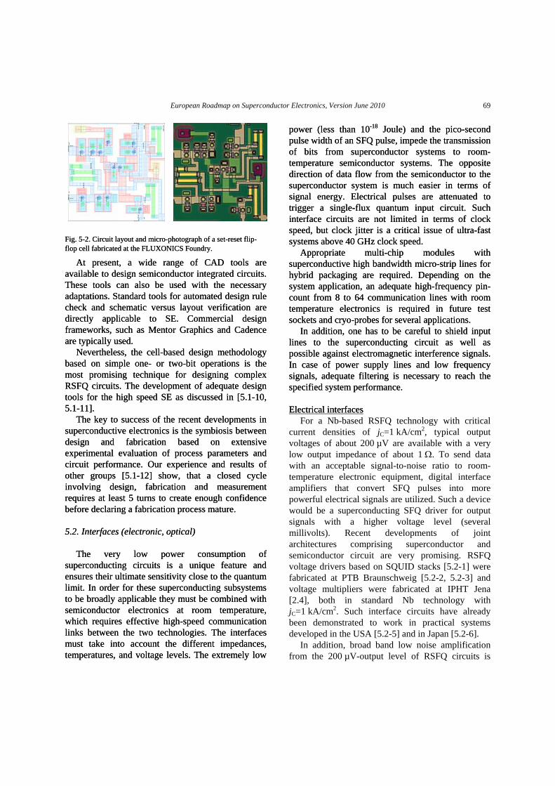
European Roadmap on Superconductor Electronics, Version June 2010 69
Fig. 5-2. Circuit layout and micro-photograph of a set-reset flip-flop cell fabricated at the FLUXONICS Foundry. Fig. 5-2. Circuit layout and micro-photograph of a set-reset flip-flop cell fabricated at the FLUXONICS Foundry.
At present, a wide range of CAD tools are available to design semiconductor integrated circuits. These tools can also be used with the necessary adaptations. Standard tools for automated design rule check and schematic versus layout verification are directly applicable to SE. Commercial design frameworks, such as Mentor Graphics and Cadence are typically used.
At present, a wide range of CAD tools are available to design semiconductor integrated circuits. These tools can also be used with the necessary adaptations. Standard tools for automated design rule check and schematic versus layout verification are directly applicable to SE. Commercial design frameworks, such as Mentor Graphics and Cadence are typically used.
Nevertheless, the cell-based design methodology based on simple one- or two-bit operations is the most promising technique for designing complex RSFQ circuits. The development of adequate design tools for the high speed SE as discussed in [5.1-10, 5.1-11].
Nevertheless, the cell-based design methodology based on simple one- or two-bit operations is the most promising technique for designing complex RSFQ circuits. The development of adequate design tools for the high speed SE as discussed in [5.1-10, 5.1-11].
The key to success of the recent developments in superconductive electronics is the symbiosis between design and fabrication based on extensive experimental evaluation of process parameters and circuit performance. Our experience and results of other groups [5.1-12] show, that a closed cycle involving design, fabrication and measurement requires at least 5 turns to create enough confidence before declaring a fabrication process mature.
The key to success of the recent developments in superconductive electronics is the symbiosis between design and fabrication based on extensive experimental evaluation of process parameters and circuit performance. Our experience and results of other groups [5.1-12] show, that a closed cycle involving design, fabrication and measurement requires at least 5 turns to create enough confidence before declaring a fabrication process mature.
5.2. Interfaces (electronic, optical) 5.2. Interfaces (electronic, optical)
The very low power consumption of superconducting circuits is a unique feature and ensures their ultimate sensitivity close to the quantum limit. In order for these superconducting subsystems to be broadly applicable they must be combined with semiconductor electronics at room temperature, which requires effective high-speed communication links between the two technologies. The interfaces must take into account the different impedances, temperatures, and voltage levels. The extremely low
power (less than 10-18 Joule) and the pico-second pulse width of an SFQ pulse, impede the transmission of bits from superconductor systems to room-temperature semiconductor systems. The opposite direction of data flow from the semiconductor to the superconductor system is much easier in terms of signal energy. Electrical pulses are attenuated to trigger a single-flux quantum input circuit. Such interface circuits are not limited in terms of clock speed, but clock jitter is a critical issue of ultra-fast systems above 40 GHz clock speed.
The very low power consumption of superconducting circuits is a unique feature and ensures their ultimate sensitivity close to the quantum limit. In order for these superconducting subsystems to be broadly applicable they must be combined with semiconductor electronics at room temperature, which requires effective high-speed communication links between the two technologies. The interfaces must take into account the different impedances, temperatures, and voltage levels. The extremely low
power (less than 10
Appropriate multi-chip modules with superconductive high bandwidth micro-strip lines for hybrid packaging are required. Depending on the system application, an adequate high-frequency pin-count from 8 to 64 communication lines with room temperature electronics is required in future test sockets and cryo-probes for several applications.
Appropriate multi-chip modules with superconductive high bandwidth micro-strip lines for hybrid packaging are required. Depending on the system application, an adequate high-frequency pin-count from 8 to 64 communication lines with room temperature electronics is required in future test sockets and cryo-probes for several applications.
In addition, one has to be careful to shield input lines to the superconducting circuit as well as possible against electromagnetic interference signals. In case of power supply lines and low frequency signals, adequate filtering is necessary to reach the specified system performance.
In addition, one has to be careful to shield input lines to the superconducting circuit as well as possible against electromagnetic interference signals. In case of power supply lines and low frequency signals, adequate filtering is necessary to reach the specified system performance. Electrical interfaces
-18 Joule) and the pico-second pulse width of an SFQ pulse, impede the transmission of bits from superconductor systems to room-temperature semiconductor systems. The opposite direction of data flow from the semiconductor to the superconductor system is much easier in terms of signal energy. Electrical pulses are attenuated to trigger a single-flux quantum input circuit. Such interface circuits are not limited in terms of clock speed, but clock jitter is a critical issue of ultra-fast systems above 40 GHz clock speed.
Electrical interfaces For a Nb-based RSFQ technology with critical
current densities of jC=1 kA/cm2, typical output voltages of about 200 µV are available with a very low output impedance of about 1 Ω. To send data with an acceptable signal-to-noise ratio to room-temperature electronic equipment, digital interface amplifiers that convert SFQ pulses into more powerful electrical signals are utilized. Such a device would be a superconducting SFQ driver for output signals with a higher voltage level (several millivolts). Recent developments of joint architectures comprising superconductor and semiconductor circuit are very promising. RSFQ voltage drivers based on SQUID stacks [5.2-1] were fabricated at PTB Braunschweig [5.2-2, 5.2-3] and voltage multipliers were fabricated at IPHT Jena [2.4], both in standard Nb technology with jC=1 kA/cm2. Such interface circuits have already been demonstrated to work in practical systems developed in the USA [5.2-5] and in Japan [5.2-6].
In addition, broad band low noise amplification from the 200 µV-output level of RSFQ circuits is

5. Enabling Technologies 70
required in several steps. Most important is the performance of the first preamplifier stage at 4.2 K. They must provide a high bandwidth (above 10 GHz), ultra-low noise, and extremely low-power consumption (below 2 mW).
A multi stage amplifier hierarchy with two or more temperature stages is most promising to meet the system specifications, e.g. total cooling power and data-rate. Fig. 5-3 shows the most advanced interface configuration of the superconducting network switch developed by ISTEC-SRL in Japan [5.2-9].
Fig. 5-3. Multi-stage interface configuration including superconducting voltage drivers and cryogenic semiconductor amplifiers (figure- courtesy of Y. Hashimoto [5.2-9]).
The bit-error rate (BER) is the most important measure for the quality of a digital data transmission system. Since the BER is related to signal-to-noise ratio, we should be able to reduce the BER by using larger signal amplitude. This is especially important in high-speed systems because the noise power increases with the bandwidth [5.2-7]. The most advanced electrical interface circuits today can provide data rates up to 25 gigabits per second with a BER lower than 10-13 errors per second [5.2-8]. This speed would enable the transfer of an entire movie DVD within only 1.5 seconds.
Electro/Optical interfaces
The most attractive signal transfer for both
directions would be the application of optical fibres, because of the extremely high data rates, low signal
losses, no electromagnetic interference and almost no heat load. Special hermetically sealed optical connectors are required and uni-traveling carrier photodiodes (UTC-PDs) [5.2-9] have been demonstrated to operate at low temperature of 4 Kelvin. Signal communication between room temperature electronics and superconductor circuits with data rates up to 40 gigabit per second has been demonstrated recently [5.2-10]. In future, for input lines WDM (Wavelength Division Multiplexed) optical technology may be used, which provides the best electro-thermal isolation.
The principal problem is the output-signal circuitry. Since there is not enough power in an SFQ data bit to directly drive ambient or cryogenic semiconductor electronics, interface circuits are required to amplify the SFQ voltage pulse. Semiconductor drive circuits consume more power than can be tolerated at the 4-Kelvin stage. One option is to communicate SFQ signals up to an intermediate temperature stage and then optically up to room temperature. There is currently a strong demand for research, but no solution known.
5.3. Cryocooling
This section considers firstly the developments in cryocooler user communities followed by a comparison of the cryocooling state-of-the-art with the targets set in the 2006 roadmap [5.3-1]. Then, the requirements as imposed by present-day super-conducting electronics are summarized and compared to the state-of-art on cryocooling. Finally, trends are reviewed, followed by a subsection on cryogenic packaging issues and a concluding discussion.
5.3.1. Cryocooler user communities In the previous roadmap, three user communities were identified (for cryocoolers with a cooling power in the range of 1 W or below): Infrared detectors, cryopumping, and space. A new cryocooler market that has developed in the last few years is the cooling of high-temperature superconducting filters in base stations for cellular phone telecommunication, mostly in USA [5.3-2]. These filters provide better filtering performance, improved gain, and less losses compared to conventional filters. The required cooling power is about 5 W @ 80 K, mostly
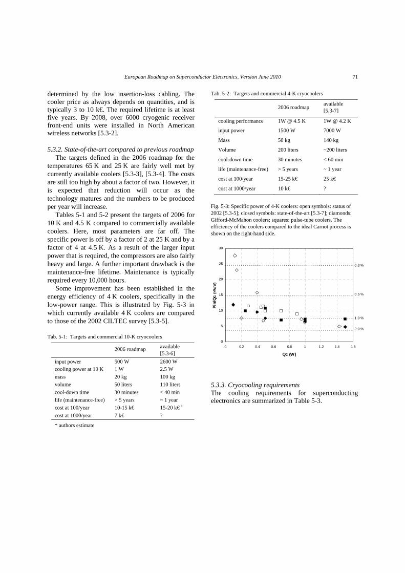
European Roadmap on Superconductor Electronics, Version June 2010 71
determined by the low insertion-loss cabling. The cooler price as always depends on quantities, and is typically 3 to 10 k€. The required lifetime is at least five years. By 2008, over 6000 cryogenic receiver front-end units were installed in North American wireless networks [5.3-2].
5.3.2. State-of-the-art compared to previous roadmap The targets defined in the 2006 roadmap for the
temperatures 65 K and 25 K are fairly well met by currently available coolers [5.3-3], [5.3-4]. The costs are still too high by about a factor of two. However, it is expected that reduction will occur as the technology matures and the numbers to be produced per year will increase.
Tables 5-1 and 5-2 present the targets of 2006 for 10 K and 4.5 K compared to commercially available coolers. Here, most parameters are far off. The specific power is off by a factor of 2 at 25 K and by a factor of 4 at 4.5 K. As a result of the larger input power that is required, the compressors are also fairly heavy and large. A further important drawback is the maintenance-free lifetime. Maintenance is typically required every 10,000 hours.
0
5
10
15
20
25
30
0 0.2 0.4 0.6 0.8 1 1.2 1.4 1.6
Qc (W)
Pin/
Qc (k
W/W
)
0.3 %
2.0 %
1.0 %
0.5 %Some improvement has been established in the
energy efficiency of 4 K coolers, specifically in the low-power range. This is illustrated by Fig. 5-3 in which currently available 4 K coolers are compared to those of the 2002 CILTEC survey [5.3-5].
Tab. 5-1: Targets and commercial 10-K cryocoolers
2006 roadmap available [5.3-6]
input power 500 W 2600 W cooling power at 10 K 1 W 2.5 W mass 20 kg 100 kg volume 50 liters 110 liters cool-down time 30 minutes < 40 min life (maintenance-free) > 5 years ~ 1 year cost at 100/year 10-15 k€ 15-20 k€ 1
cost at 1000/year 7 k€ ?
* authors estimate
Tab. 5-2: Targets and commercial 4-K cryocoolers
2006 roadmap available [5.3-7]
cooling performance 1W @ 4.5 K 1W @ 4.2 K
input power 1500 W 7000 W
Mass 50 kg 140 kg
Volume 200 liters ~200 liters
cool-down time 30 minutes < 60 min
life (maintenance-free) > 5 years ~ 1 year
cost at 100/year 15-25 k€ 25 k€
cost at 1000/year 10 k€ ? Fig. 5-3: Specific power of 4-K coolers: open symbols: status of 2002 [5.3-5]; closed symbols: state-of-the-art [5.3-7]; diamonds: Gifford-McMahon coolers; squares: pulse-tube coolers. The efficiency of the coolers compared to the ideal Carnot process is shown on the right-hand side.
5.3.3. Cryocooling requirements The cooling requirements for superconducting electronics are summarized in Table 5-3.

5. Enabling Technologies 72
Tab. 5-3: Cooling requirements for superconducting electronics
tempe-rature
cooling power SE application
10 - 100 mW
small HTS SQUIDs (mm2) 10 - 20 mW; larger SQUIDs (cm2) 50 - 100 mW; 70 - 80
K 2-10 W HTS filters for telecom
30 - 40 K
10 – 20 mW
digital HTS circuits with small complexity and failure tolerant, e.g. sampler and DigiSQUID
20 K ? MgB2 devices, however, junction technology not yet available
8 - 10 K 0.1 – 0.2 W
NbN, ADC, voltage standards, perhaps detectors
4 – 5 K 0.1 – 0.2 W
Nb-based RSFQ and voltage standards*
3 – 5 K 0.3 - 3 mW
LTS SQUIDs, SIS mixers, hot-electron bolometers, single-photon detectors.
0.1 -0.3 K
20-100 μW transition edge sensors
50 mK 10 μW micro bolometers
10 mK μW qubits (quantum computing)
* The cooling power required for RSFQ may be reduced by more advanced circuit design, see text.
On-chip power consumption
The electrical power consumption of superconducting electronics cooled at 4.2 K can be estimated quite accurately from recent developments of the most complex digital circuits fabricated to date in the world, in particular in Japan. State-of-the-art is 180-350 nW/junction [5.3-8 to 5.3-10]. The most optimistic expectations in the near future are of the order of 10 nW/junction [5.3-11].
In the case of low- to medium-complexity circuits (≈ 100 to ≈ 1000 junctions), the maximum power that is dissipated on-chip is lower than 300 µW. This corresponds to a wide range of circuits, concerning most of detectors and specific digital electronics circuits for dedicated tasks, like digital SQUIDs. For more complex circuits, like supercomputer chips, readout of detectors, routers for telecommunications, the currently expected on-chip power dissipation is of the order of 1.5-3 mW for complex chips (104
junctions) to 15-30 mW for highly integrated chips (105 junctions).
For operations of circuits at higher temperatures like 20 to 80 K, the bias current of digital circuits should increase linearly with temperature in the most pessimistic case to stay higher than the thermal noise. Nevertheless, no high-complexity circuits are expected to work at these temperatures in the near future. Consequently, the maximum value of 300 µW given above will likely not increase above 6 mW at 80 K. Off-chip power consumption
Concerning off-chip power dissipation, one can separate applications in two main categories: a) the ones that require only dc wiring and low-frequency signals, and b) the ones that require microwave frequencies and/or high data rates. For the first kind, the amplifiers and transducers that carry the data from the inside of the cooler to room temperature will consume a low power. Consequently, on-chip power consumption will dominate. For the second kind of applications, things are really different: the simple use of one microwave amplification channel will lead to a power consumption of several mW, 2 mW for a reasonable 20 dB gain in the best case, 10 mW as a more typical value. Nevertheless, even complex circuits will not require many channels since most of the data processing is done on-chip. A reasonable estimate of 10 input/output channels corresponds to 100 mW of power consumption, that should be enough to meet a large part of the needs. Cooler interference
A further important point is the issue of cooler interference (temperature stability, vibrations, EMI). Currently, SE electronics can be operated with 4 K coolers and first demonstrations were made with voltage standards. However, cooler interference appears to be the limiting factor with respect to the overall system noise levels.
5.3.4. Trends in cryocooling Lifetime and reliability
Long-life compressors incorporating flexure bearings and clearance seals are now available in mechanical coolers for the HTS temperature range. Lifetimes of at least 5 years are specified. In order to
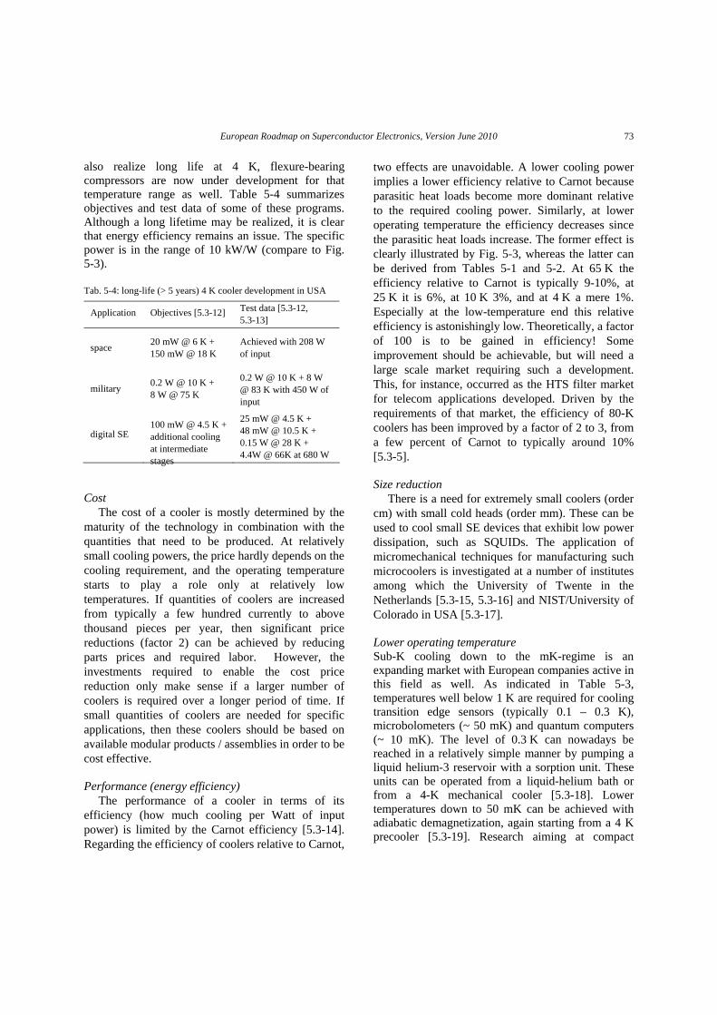
European Roadmap on Superconductor Electronics, Version June 2010 73
also realize long life at 4 K, flexure-bearing compressors are now under development for that temperature range as well. Table 5-4 summarizes objectives and test data of some of these programs. Although a long lifetime may be realized, it is clear that energy efficiency remains an issue. The specific power is in the range of 10 kW/W (compare to Fig. 5-3). Tab. 5-4: long-life (> 5 years) 4 K cooler development in USA
Application Objectives [5.3-12] Test data [5.3-12, 5.3-13]
space 20 mW @ 6 K + 150 mW @ 18 K
Achieved with 208 W of input
military 0.2 W @ 10 K + 8 W @ 75 K
0.2 W @ 10 K + 8 W @ 83 K with 450 W of input
digital SE 100 mW @ 4.5 K + additional cooling at intermediate stages
25 mW @ 4.5 K + 48 mW @ 10.5 K + 0.15 W @ 28 K + 4.4W @ 66K at 680 W i
Cost
The cost of a cooler is mostly determined by the maturity of the technology in combination with the quantities that need to be produced. At relatively small cooling powers, the price hardly depends on the cooling requirement, and the operating temperature starts to play a role only at relatively low temperatures. If quantities of coolers are increased from typically a few hundred currently to above thousand pieces per year, then significant price reductions (factor 2) can be achieved by reducing parts prices and required labor. However, the investments required to enable the cost price reduction only make sense if a larger number of coolers is required over a longer period of time. If small quantities of coolers are needed for specific applications, then these coolers should be based on available modular products / assemblies in order to be cost effective. Performance (energy efficiency)
The performance of a cooler in terms of its efficiency (how much cooling per Watt of input power) is limited by the Carnot efficiency [5.3-14]. Regarding the efficiency of coolers relative to Carnot,
two effects are unavoidable. A lower cooling power implies a lower efficiency relative to Carnot because parasitic heat loads become more dominant relative to the required cooling power. Similarly, at lower operating temperature the efficiency decreases since the parasitic heat loads increase. The former effect is clearly illustrated by Fig. 5-3, whereas the latter can be derived from Tables 5-1 and 5-2. At 65 K the efficiency relative to Carnot is typically 9-10%, at 25 K it is 6%, at 10 K 3%, and at 4 K a mere 1%. Especially at the low-temperature end this relative efficiency is astonishingly low. Theoretically, a factor of 100 is to be gained in efficiency! Some improvement should be achievable, but will need a large scale market requiring such a development. This, for instance, occurred as the HTS filter market for telecom applications developed. Driven by the requirements of that market, the efficiency of 80-K coolers has been improved by a factor of 2 to 3, from a few percent of Carnot to typically around 10% [5.3-5]. Size reduction
There is a need for extremely small coolers (order cm) with small cold heads (order mm). These can be used to cool small SE devices that exhibit low power dissipation, such as SQUIDs. The application of micromechanical techniques for manufacturing such microcoolers is investigated at a number of institutes among which the University of Twente in the Netherlands [5.3-15, 5.3-16] and NIST/University of Colorado in USA [5.3-17]. Lower operating temperature Sub-K cooling down to the mK-regime is an expanding market with European companies active in this field as well. As indicated in Table 5-3, temperatures well below 1 K are required for cooling transition edge sensors (typically 0.1 – 0.3 K), microbolometers (~ 50 mK) and quantum computers (~ 10 mK). The level of 0.3 K can nowadays be reached in a relatively simple manner by pumping a liquid helium-3 reservoir with a sorption unit. These units can be operated from a liquid-helium bath or from a 4-K mechanical cooler [5.3-18]. Lower temperatures down to 50 mK can be achieved with adiabatic demagnetization, again starting from a 4 K precooler [5.3-19]. Research aiming at compact

5. Enabling Technologies 74
adiabatic demagnetization coolers, mostly for space applications, is carried out in USA [5.3-20] as well as in Europe [5.3-21, 5.3-22]. It should, however, be realized that with this technique most SE applications will require substantial magnetic shielding [5.3-21]. In order to arrive at 10 mK, as required for quantum computing, a dilution refrigerator is required [5.3-19, 5.3-23]. Low-noise coolers
Vibrations can be drastically reduced by using back-to-back compressors, active vibration control, and pulse-tube cold heads with no moving parts in the cold end. Extremely low levels of vibrations are achievable by using thermally operated sorption compressors combined with Joule-Thomson expansion stages [5.3-24].
5.3.5. Cryogenic packaging Packaging issues strongly depend on the specific
application. In general, the aim is to have compact and low-cost coolers to be integrated with the superconducting system. In addition, specific SE applications may require very low interference levels. Size (mass and volume)
As a rough indication, it is felt acceptable for the SE community if the cooler takes 10% of the system volume and similarly it may cost 10% of the whole system. In order to realize these small and cheap coolers, it is essential to operate at higher temperatures and/or at lower cooling powers.
At a given operating temperature, the volume of a cooler increases with the required heat lift as a power law in which the exponent e.g. at 65 K is about 0.7 [5.3-5]. Twice the cooling power, therefore, will result in a cooler volume increase of 60%. Size also reduces dramatically as the operating temperature is increased. Within the temperatures and power ranges relevant to SE, the mass decreases by about 5% for every K increase in operating temperature! [5.3-5]. Operating temperature
There is no general answer to the question how to realize a higher operating temperature; it is strongly depending on the application. Nevertheless, one can set up some global guideline, unfortunately indicating that there is not much margin to increase the operating temperature:
(1) In digital applications, if many junctions are used and a very low bit-error rate is required, it typically comes down to a maximum operating temperature of around 50% of Tc, e.g. 40-50 K for YBCO, 4-5 K for Nb, 8-10 K for NbN. (2) SQUIDs can be operated up to 80-90% of Tc. At higher temperatures, all parameters become too temperature dependent, and any temperature fluctuation immediately translates in a significant change of the electrical parameters. (3) Detectors: superconducting devices are used in this field only for measurements with maximum resolution: thus the temperature should be kept as low as possible. Required cooling power A lower on-chip consumption can be obtained by reducing the critical current (and consequently the size) of the Josephson junctions. At 4 K, a maximum reduction of on-chip consumption of 4 to 16 can be expected in the best case, departing from a critical current in the range 100-200 µA to reach 50 µA.
A lower off-chip consumption can be realized by reducing the current flowing through the connecting lines. This can be established by recycling as much as possible the current in the superconducting circuit. A reduction of power dissipation by a factor of 100 can be expected in bias wires from first encouraging experimental results [5.3-25].
Furthermore, parasitics can be reduced mostly by reducing the conductive heat load through the wiring. In digital systems operating at temperatures below about 20 K, HTS may be used for bias wiring up to fairly high currents [5.3-26]. The most difficult part of the dissipated power to reduce is the one consumed by the amplifiers or optoelectronic transducers used at the output of the superconducting chip, e.g. by interfaces to the external room-temperature world. The choice of the temperature of operation of these transducers or amplifiers is crucial with regards to the thermal budget.
Moreover, for microwave communication and associated signal processing, an important aspect is low-loss signal coupling of the outside world to the cryogenic inside. Usually, low insertion losses are required implying high thermal losses in case of straightforward electric connections. Alternative connecting schemes will have to be developed, e.g. by capacitive and/or inductive coupling facilitating a thermal interrupt. First experimental results with

European Roadmap on Superconductor Electronics, Version June 2010 75
antennas used in near-field configuration are encouraging for transmitting through the cryocooler stages, with no thermal conductive loss, narrow-band 10 GHz microwave signals with losses lower than 2 dB over a 1 GHz bandwidth [5.3-27].
The required cooling power can also be reduced by incorporating multi-stage coolers. Heat can be removed more efficiently at higher temperatures, and thus the heat load to the coldest stage can be significantly reduced. In addition, when using low-frequency pulse-tube coolers down to 4 K or below, some “free” cooling can be recovered at temperature levels between 20 K and 4 K using heat intercepts thermally anchored to the regenerator and/or the pulse tube [5.3-28 to 5.3-30]. Low-interference interfacing
In many cases, coolers generate noise: electromagnetic interference (EMI), mechanical vibrations and/or temperature fluctuations. Correct mounting of the compressor in the application is very important in this respect.
The simplest approach for the suppression of cooler interference is to switch off the cooler at the moment the superconducting device is to be used. There are two problems: firstly, the cooler should not be switched off too frequently because that will seriously limit its lifetime, and secondly, the temperature of the device will slowly increase (thermal drift). Both problems can be solved by incorporating a sufficiently large thermal buffer. To stabilize the temperature it is best to apply a buffer with a phase change material involved [5.3-31].
Besides separation in time, cooler and device can also be separated in space. A large separation can be realized by using a forced circulation of helium [5.3-32].
5.3.6. Discussion Cryocoolers, allowing for cryogen-free operation
of superconducting electronics (SE), are now available on the market for the whole temperature range relevant to SE (0.3 – 80 K). The reliability of these coolers has been dramatically improved over the last decade and nowadays lifetimes of over 5 years are specified. Cost has been reduced but should decrease by another factor of two in order to reach a price level that is considered acceptable compared to the overall system costs. This further reduction in
price is expected to occur as technology matures and numbers produced increase.
The main drawbacks of commercially available cryocoolers are their poor efficiency at low temperatures and at low cooling powers, and the interference they cause in SE applications. Energy efficiency not only is relevant from a power input point of view, it also directly relates to mass, size and cost of the system. At relatively high temperatures (> 20 K), the available cooler efficiencies are quite acceptable, whereas at lower temperatures there is quite some room for improvement. At 4 K, cryocoolers typically operate at only 1% of their thermodynamic limit. Obviously, parasitic heat loads are important especially at lower temperatures, but the performance gap between high-power coolers (e.g. helium liquefiers) that operate around 30% of the thermodynamic limit and SE coolers is far too big.
Performance at low powers and at low temperatures seems to be limited by the technology used (e.g. regenerator performance). In that respect, a technology breakthrough is needed.
Interference is mostly caused by the mechanical principle of operation (mechanical compressors and often moving displacers in the cold head). Vibrations are generated and the driving currents and moving magnetic material cause electromagnetic interference. Specifically for sensitive SE applications (detectors, SQUIDs) low-noise coolers are needed. These can be realized by incorporating noise-cancellation techniques in mechanical operation, or by developing non-mechanical cryogenic cooling techniques. Table 5-5 shows the cryocooler development timeline in which the applications considered in Table 5-3 are reduced to five main types. Coolers for passive HTS applications, such as filters, that can tolerate “some” cooler noise, are close to maturity already. Further development mainly is on cost. The required development of the other cooler types towards maturity directly results from the timelines of the various SE applications as presented in the other sections of this roadmap.
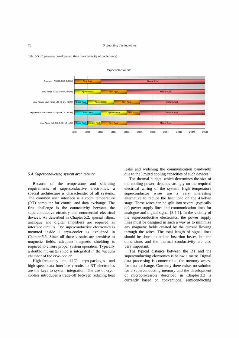
5. Enabling Technologies 76
5.4. Superconducting system architecture
Because of the temperature and shielding requirements of superconductive electronics, a special architecture is characteristic of all systems. The common user interface is a room temperature (RT) computer for control and data exchange. The first challenge is the connectivity between the superconductive circuitry and commercial electrical devices. As described in Chapter 5.2, special filters, analogue and digital amplifiers are required as interface circuits. The superconductive electronics is mounted inside a cryo-cooler as explained in Chapter 5.3. Since all these circuits are sensitive to magnetic fields, adequate magnetic shielding is required to ensure proper system operation. Typically a double mu-metal shied is integrated in the vacuum chamber of the cryo-cooler.
High-frequency multi-I/O cryo-packages and high-speed data interface circuits to RT electronics are the keys to system integration. The use of cryo-coolers introduces a trade-off between reducing heat
leaks and widening the communication bandwidth due to the limited cooling capacities of such devices.
The thermal budget, which determines the size of the cooling power, depends strongly on the required electrical wiring of the system. High temperature superconductor wires are a very interesting alternative to reduce the heat load on the 4 kelvin stage. These wires can be split into several (typically dc) power supply lines and communication lines for analogue and digital signal [5.4-1]. In the vicinity of the superconductive electronics, the power supply lines must be designed in such a way as to minimize any magnetic fields created by the current flowing through the wires. The total length of signal lines should be short, to reduce insertion losses, but the dimensions and the thermal conductivity are also very important.
The typical distance between the RT and the superconducting electronics is below 1 metre. Digital data processing is connected to the memory access for data exchange. Currently there exists no solution for a superconducting memory and the development of microprocessors described in Chapter 3.2 is currently based on conventional semiconducting
Tab. 5-5: Cryocooler development time line (maturity of cooler only)
Cryocooler for SE
Basic R&D
Basic R&D
Basic R&D
Applied R&D
Applied R&D
Applied R&D
Applied R&D
First Appl.
First Appl.
First Appl.
First Appl.
First Appl.
Mature Appl.
Mature Appl.
Mature Appl.
Mature Appl.
Mature Appl.
2010 2011 2012 2013 2014 2015 2016 2017 2018 2019 2020
Low -Noise Sub-K (<0.3K, <0.1mW)
High-Pow er Low -Noise LTS (4-5K, 0.1-0.2W)
Low -Pow er Low -Noise LTS (3-5K, <3mW)
Low -Noise HTS (70-80K, <0.1W)
Standard HTS (70-80K, 2-10W)

European Roadmap on Superconductor Electronics, Version June 2010 77
memory at RT. To reduce access time and latency, the distance between memory and processor needs to be small, which can be solved by cryogenic CMOS implementations of memory directly connected to RSFQ chips [5.4-3].
As mentioned in Chapter 5.2, the use of optical fibers together with hermetically sealed optical connectors relaxes the restrictions caused by high speed communication lines.
Fig. 5-6 shows a fully operational example of a cyro-cooled digital switch system demonstrated at NEC in Japan [5.4-4]. The system utilizes a two stage GM cryo-cooler from Sumitomo Ltd. with a cooling power of 1 W at 4.2 K and 31 W at 40 K. The 32 signal and supply lines are semi-rigid coaxial cables with a bandwidth of more than 25 GHz. The probe head carries a MCM sample carrier and is equipped with a two layer magnetic shield.
Fig. 5-6 Cryo-cooled system configuration for the switch system developed at NEC in Japan [5.4-3]
As an example, a Josephson voltage standard
made by Supracon AG is shown in Fig. 5.7. The system is integrated with a commercial 4 Kelvin cryo-cooler, and equipped them with room-temperature interface electronics controlled by graphical user interface. This metrological standard demonstrates the maturity of fully cryo-cooled superconductor technology operating at 4 Kelvin.
Fig. 5-7. The cryo-cooled Josephson voltage standard, fabricated ad Supracon AG. The system comsists of the following components: 1: pulse tube cooler with a SIS Josephson junction array and the 75 GHz microwave electronics installed in the 19” rack, 2: control electronics, 3: source looking counter, 4: null detector, 5: 3-channel polarity reversal switch, 6: sensors for temperature, pressure and humidity, 7: computer control, 8: 2 kW compressor unit.
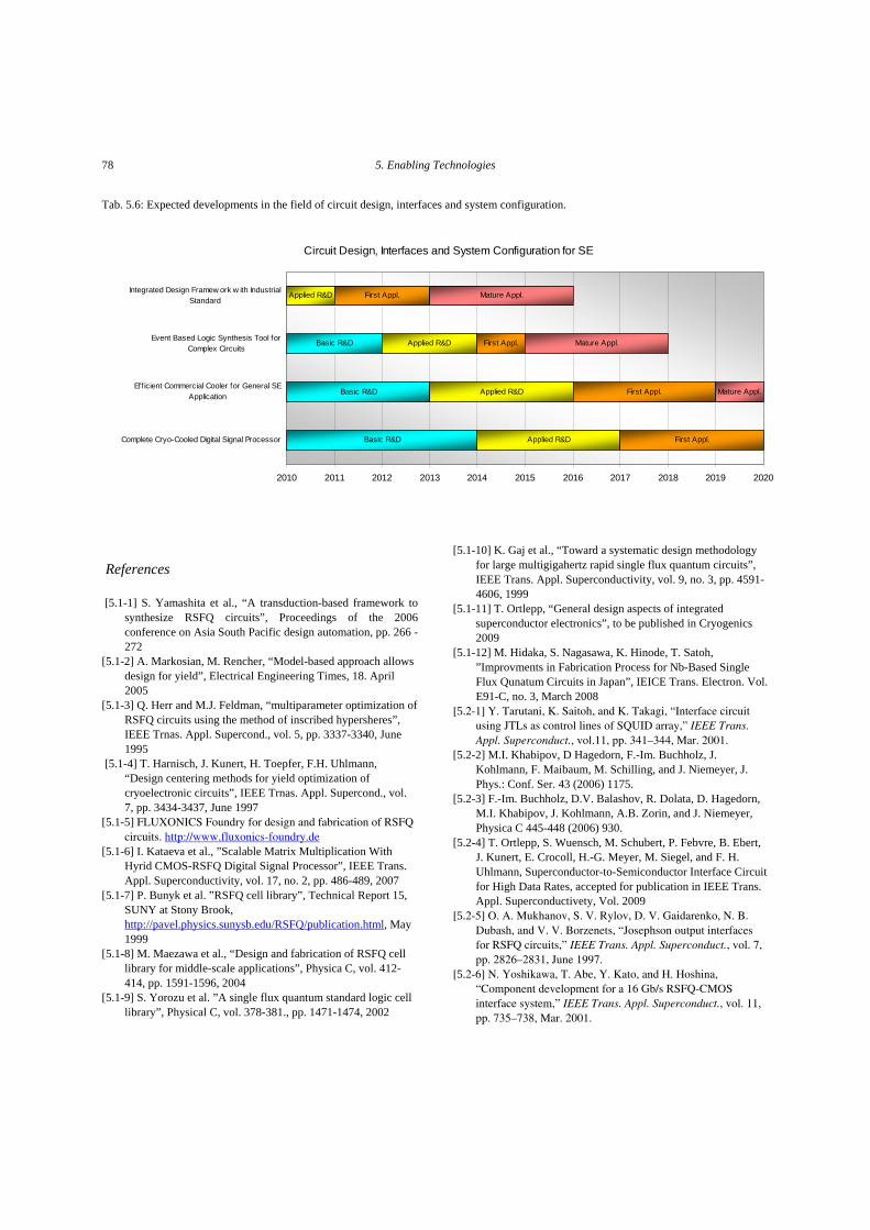
5. Enabling Technologies 78
Circuit Design, Interfaces and System Configuration for SE
Basic R&D
Basic R&D
Basic R&D
Applied R&D
Applied R&D
Applied R&D
Applied R&D
First Appl.
First Appl.
First Appl.
First Appl.
Mature Appl.
Mature Appl.
Mature Appl.
2010 2011 2012 2013 2014 2015 2016 2017 2018 2019 2020
Complete Cryo-Cooled Digital Signal Processor
Eff icient Commercial Cooler for General SEApplication
Event Based Logic Synthesis Tool forComplex Circuits
Integrated Design Framew ork w ith IndustrialStandard
References
[5.1-1] S. Yamashita et al., “A transduction-based framework to synthesize RSFQ circuits”, Proceedings of the 2006 conference on Asia South Pacific design automation, pp. 266 - 272
[5.1-2] A. Markosian, M. Rencher, “Model-based approach allows design for yield”, Electrical Engineering Times, 18. April 2005
[5.1-3] Q. Herr and M.J. Feldman, “multiparameter optimization of RSFQ circuits using the method of inscribed hypersheres”, IEEE Trnas. Appl. Supercond., vol. 5, pp. 3337-3340, June 1995
[5.1-4] T. Harnisch, J. Kunert, H. Toepfer, F.H. Uhlmann, “Design centering methods for yield optimization of cryoelectronic circuits”, IEEE Trnas. Appl. Supercond., vol. 7, pp. 3434-3437, June 1997
[5.1-5] FLUXONICS Foundry for design and fabrication of RSFQ circuits. http://www.fluxonics-foundry.de
[5.1-6] I. Kataeva et al., ”Scalable Matrix Multiplication With Hyrid CMOS-RSFQ Digital Signal Processor”, IEEE Trans. Appl. Superconductivity, vol. 17, no. 2, pp. 486-489, 2007
[5.1-7] P. Bunyk et al. ”RSFQ cell library”, Technical Report 15, SUNY at Stony Brook, http://pavel.physics.sunysb.edu/RSFQ/publication.html, May 1999
[5.1-8] M. Maezawa et al., “Design and fabrication of RSFQ cell library for middle-scale applications”, Physica C, vol. 412-414, pp. 1591-1596, 2004
[5.1-9] S. Yorozu et al. ”A single flux quantum standard logic cell library”, Physical C, vol. 378-381., pp. 1471-1474, 2002
[5.1-10] K. Gaj et al., “Toward a systematic design methodology for large multigigahertz rapid single flux quantum circuits”, IEEE Trans. Appl. Superconductivity, vol. 9, no. 3, pp. 4591-4606, 1999
[5.1-11] T. Ortlepp, “General design aspects of integrated superconductor electronics”, to be published in Cryogenics 2009
[5.1-12] M. Hidaka, S. Nagasawa, K. Hinode, T. Satoh, ”Improvments in Fabrication Process for Nb-Based Single Flux Qunatum Circuits in Japan”, IEICE Trans. Electron. Vol. E91-C, no. 3, March 2008
[5.2-1] Y. Tarutani, K. Saitoh, and K. Takagi, “Interface circuit using JTLs as control lines of SQUID array,” IEEE Trans. Appl. Superconduct., vol.11, pp. 341–344, Mar. 2001.
[5.2-2] M.I. Khabipov, D Hagedorn, F.-Im. Buchholz, J. Kohlmann, F. Maibaum, M. Schilling, and J. Niemeyer, J. Phys.: Conf. Ser. 43 (2006) 1175.
Tab. 5.6: Expected developments in the field of circuit design, interfaces and system configuration.
[5.2-3] F.-Im. Buchholz, D.V. Balashov, R. Dolata, D. Hagedorn, M.I. Khabipov, J. Kohlmann, A.B. Zorin, and J. Niemeyer, Physica C 445-448 (2006) 930.
[5.2-4] T. Ortlepp, S. Wuensch, M. Schubert, P. Febvre, B. Ebert, J. Kunert, E. Crocoll, H.-G. Meyer, M. Siegel, and F. H. Uhlmann, Superconductor-to-Semiconductor Interface Circuit for High Data Rates, accepted for publication in IEEE Trans. Appl. Superconductivety, Vol. 2009
[5.2-5] O. A. Mukhanov, S. V. Rylov, D. V. Gaidarenko, N. B. Dubash, and V. V. Borzenets, “Josephson output interfaces for RSFQ circuits,” IEEE Trans. Appl. Superconduct., vol. 7, pp. 2826–2831, June 1997.
[5.2-6] N. Yoshikawa, T. Abe, Y. Kato, and H. Hoshina, “Component development for a 16 Gb/s RSFQ-CMOS interface system,” IEEE Trans. Appl. Superconduct., vol. 11, pp. 735–738, Mar. 2001.
European Roadmap on Superconductor Electronics, Version June 2010 79
[5.3-17] P.E. Bradley et al., in: S.D. Miller and R.G. Ross jr. (Eds.), Cryocoolers 15 ICC Press Boulder, USA. isbn. 13-978-1-934021-01-9. (2009, pp. 425-432).
[5.2-7] Naoki Harada, Nobuyuki Yoshikawa, Akira Yoshida, and Naoki Yokoyama, Josephson Latching Driver With a Low Bit-Error Rate, IEEE Trans. Appl. Supercond., Vol. 14, no. 4, 2004 [5.3-18] L. Duband, L. Clerc, A. Ravex, SOCOOL: Adv Cryo Eng
47B, AIP Conf proc. 613, (2002) 1233-1237. [5.2-8] H. Ito, T. Furuta, S. Kodama, and T. Ishibashi, “InP/InGaAs unitravelling- carrier photodiode with 310 GHz bandwidth,” Electron. Lett., vol.36, no.21, pp.1809–1810, Oct. 2000.
[5.3-19] www.vericold.com [5.3-20] P. Shirron et al., Cryogenics 44 (2004) 581-588. [5.3-21] I.D. Hepburn et al., “Design and development of a space
engineering model cryogen free ADR for future ESA space missions”, proceedings ICEC 21, 2006, 323-326
[5.2-9] Y. Hashimoto et al.,” Implementation and Experimental Evaluation of a Cryo-cooled System Prototype for High throughput SFQ Digital Applications”, IEEE Trans. Appl. Superconductivity, vol. 17, no. 2, pp. 546-551, 2007
[5.3-22] J.M. Duval, N. Luchier, L. Duband, A. Sirbi, in: S.D. Miller and R.G. Ross jr. (Eds.), Cryocoolers 15 ICC Press Boulder, USA. isbn. 13-978-1-934021-01-9. (2009, pp. 505-512).
[5.2-10] Y. Hashimoto, S. Yorozu, Y. Kameda, “Development of Cryopackaging and I/OTechnologies for High-SpeedSuperconductive Digital Systems”, IEICE Trnas. Electron., Vol. E91-C, no. 3, March 2008
[5.3-23] www.leidencryogenics.com [5.3-24] J.F. Burger et al, (2007), Rev. Sci. Instrum. 78 (6) 2007
065102. [5.3-1] H.J.M. ter Brake et al., Physica C, 439 (2006), 1-41. [5.3-2] B.A. Willemsen, “Practical Cryogenic Receiver Front Ends
for Commercial Wireless Applications”, to be published in IEEE MTT-S Digest, 2009.
[5.3-25] T.V. Filippov, A. Sahu, S. Sarwana, D. Gupta, “Serially biased components for digital-RF receiver”, Proc. Appl. Supercond. Conf., 2008, to be publ. in IEEE T-Mag.
[5.3-3] Based on data of Thales Cryogenics LSF 9320 split Stirling cooler and Sunpower Cryotel MT integral Stirling cooler. Pulse-tube coolers typically have a 20% higher mass and 25% lower efficiency.
[5.3-26] R.J. Webber, J. Delmas, B.H. Moeckly, “Ultra-low heat leak YBCO superconducting leads for cryoelectronic applications”, Proc. Appl. Supercond. Conf., 2008 to be publ.in IEEE T-Mag.
[5.3-4] Based on data of AIM SL400 split Stirling cooler and Sunpower Cryotel LT integral Stirling cooler
[5.3-27] D. Bouis, P. Febvre, Int. J. Infrared and Millimeter Waves 29 (2008) 1156-1162.
[5.3-5] H.J.M. ter Brake, G.F.M. Wiegerinck, Cryogenics, 42, (2002) 705-718.
[5.3-28] Patent: US 6,915,642 B2 Jul.12,2005 [5.3-29] A. Ravex et al., in: S.D. Miller and R.G. Ross jr. (Eds.),
Cryocoolers 14, ICC Press Boulder, USA. isbn. 1-934021-00-8, (2007, pp. 157-162).
[5.3-6] Based on data of Sumitomo model DE-204 SL 6.5K Lab [5.3-7] Based on data of Cryomech model PT 410 and Sumitomo
model SRDK-408D2 [5.3-30] Wang C, Cryogenics 48 (2008) 154-59) [5.3-8] H. Park et al. "Design, Implementation, and On-Chip High-
Speed Test of an SFQ Half-Precision Floating-Point Adder," IEEE/CSC and ESAS News Forum, No. 6, October 2008; submitted to IEEE Trans. Appl. Supercond.
[5.3-31] A.P. Rijpma et al. Cryogenics 45 (2005) 231-239. [5.3-32] A.P. Rijpma et al., Cryogenics, 48 (2008) 61-67. [5.4-1] F. Futura and K. Saitoh, “A Study for an Improved Design
of Front-End Circuit of Superconducting Analog-to-Digital Converter”, IEEE Trans. Appl. Superconductivity, vol. 15, no. 2, pp. 445-448, 2005
[5.3-9] O. Mukhanov et al. IEICE Trans. Electron. E91-C, No. 3 (2008) 306-317.
[5.3-10] A. Herr, IEICE Trans. Electron. E91-C, No. 3 (2008) 293-305.
[5.4-2] O.A. Mukhanov, D. Kirichenko, I.V. Vernik, T.V. Filippov, A. Kirichenko, R. Webber, V. Dotsenko, A. Talalaevskii, J.C. Tang, A. Sahu, P. Schevchenko, R. Miller, S.B. Kaplan, S. Sarwana, D. Gupta, IEICE Trans. Electron. 91E-C, 293-305, 2008
[5.3-11] N. Takagi et. al., IEICE Trans. Electron. E91-C, No. 3 (2008) 350-355.
[5.3-12] T. Nast et al. in: S.D. Miller and R.G. Ross jr. (Eds.), Cryocoolers 14, ICC Press Boulder, USA. isbn. 1-934021-00-8, (2007, pp. 33-40).
[5.4-3] Q. Liu et al., “Latency and Power Measurements on a 64-kb Hybrid Josephson-CMOS Memory “, IEEE Trans. Appl. Superconductivity, vol. 17, no. 2, pp. 526-529, 2007 [5.3-13] R.J. Webber et al. “Integration of a 4-stage 4K pulse-tube
cryocooler laboratory prototype with a superconducting IC”, Proc. Appl. Supercond. Conf., 2008, to be publ. in IEEE T-Mag.
[5.4-4] Y. Hashimotol., “Cryopackaging and I/O Technologies for High-Speed Superconductive Digital Systems“,IEICE Transactions on Electronics, vol. E91-C(3), 325-332, 2008
[5.3-14] H.J.M. ter Brake (2000), in: H. Weinstock (Ed.), Applications of Superconductivity Amsterdam, the Netherlands: Kluwer Academic Publishes. isbn. 0-7923-6113-X. 2000, 561-639.
[5.3-15] P.P.P.M. Lerou et al., J. Micromech. and Microeng. 16 (2006) 1919-1925.
[5.3-16] P.P.P.M. Lerou et al., J. Micromech. and Microeng. 17 (2007) 1956-1960.

80 European SE Research Vision 8
6. European SE Research Vision
6.1. Assessment of the current status
Superconductivity already plays a very important role in scientific measurement techniques and ultra-sensitive detectors or on the large scale for experiments like the Large Hadron Collider or the development of fusion reactors. Such experiments would not even be feasible without superconductor technology. In the future, a growing number of superconductor applications in science and industry can be expected.
The European expertise in basic science concerning superconductivity and in material science is strong. Also in the area of applying superconductivity in high energy technology, health care, prospecting, standardization and measurement, Europe is still competitive. But with the current level of support, Europe is in danger to loose ground in the areas of health care and prospecting relative to the competitors in the USA and Japan.
In the important area of information and communication technology, Europe has already lost ground and urgently needs to close the gap to the USA and Japan. These countries have continuously maintained research programs for exploiting the unique features of Superconductive Electronics (SE). In Europe, only the FLUXONICS platform – implemented by means of the European Community - aims at bringing together actors from industry, SMEs, and research organizations such as universities in the field of superconductive electronics
As has been outlined in the previous sections, superconductive electronics is of potential impact in a variety of fields which determine the contemporary way of life as well as its quality: - Resources and Environment, - Security and mobility, - Information and Communication Technology, - Improved Production Processes, - Health Care, - Standardization and measurement.
With the appropriate support, the European position can be transformed into leadership in all of these fields. It would be an effective contribution to strengthening the future position of the European industry.
In the following, the R&D targets for Europe are specified and necessary steps on the road towards these aims are outlined. With research and development in the identified topics, Europe can reach the international status of SE.
6.2. Superconductive Electronics Research Domains
In order to turn the advantages of superconductivity into effective applications, research on different levels is necessary. These levels range from fundamental considerations to high-tech fabrication, from training of engineers to the dissemination of knowledge. It includes work in the field of applied research where phenomena are investigated under real-life conditions.
Essential research domains for SE are identified as: - Basics and Fundamentals, - Materials, - Process and Design Technology, - System Cooling, - System Interfacing. - SE Applications (Radiation Detection, Digital
Electronics, Magnetic-Field Sensing, Metrology, Passive Microwave Techniques).
6.3. Superconductive Electronics Application Domains
Superconductive Electronics is of societal impact in the following application domains: - Industrial, - Scientific/Governmental, - Medical, - Infrastructural. The next sections describe a projection of beneficial impact in the domains. Industrial One of the goals of research under the EU’s research programs consists in improving the competitiveness

European Roadmap on Superconductive Electronic, Version June 2010 81
of European industry. SE can support this aim by enabling - high-speed ICT components with low energy
consumption, - non-destructive material evaluation for quality
assurance, - IR and THz imaging technology for security,
pharmaceutical and chemical industry, - quality assurance by means of standardization /
measurements, - communication and cryptography. Scientific / governmental Both sectors of this domain can benefit from the advances SE offers through its unique capabilities of measuring physical quantities, controlling processes, and perceiving responsibilities of public administration. The impact is already strong in important fields such as - scientific instrumentation, - passive security screening, - identification of substances. Medical Medical applications are strongly connected with the superior features of measuring tiny and faint signals. The particular application potential in the medical domain, given in: - imaging of objects and markers, - new instrumentation for genomics and
proteomics, - diagnostics of brain and heart signals, - identification of substances including low-field
MRI, - cell and drug spectroscopy. Many of these methods are non-invasive and allow enhancing the productivity of medical diagnosis, which is a unique advantage of SE. Infrastructural In the domain of infrastructure, essential effects can be expected by a wide exploitation of the data sensing capabilities of SE. One example is given by avoiding accidents by preventive - non-destructive material evaluation for safety. In the field of information infrastructure which is known to “underpin economic development in all EU
regions” [6-1], the high speed processing capabilities of digital SE will enable - components for broadband communication as
routers and switches, - A/D and D/A converters, - Concerning the search for resources, SE today
contributes significantly in the - geological exploration, - detection of raw materials, minerals, ground
water, - environmental protection, - imaging of archaeological objects.
6.4. R&D Objectives of SE - meeting Europe’s major Challenges
R&D work, directed towards applications, will inevitably be of benefit for European Society in all the application domains described above. From today’s view, the effects will contribute to meet the general goals and challenges of the European Society which are outlined e.g. in [6-2]. In the following paragraphs, this is briefly illustrated. Competitiveness of European Industry The introduction of SE will have impact on production issues mainly, but not only, through superior diagnostics will it enable the highest level quality assurance and precision. Broad-band Communication Tomorrow’s networks as well as the desired ubiquitous access to digital content and the “Access for All”-initiative is based on the existence of a powerful infrastructure for data transmission. SE can provide high-speed digital electronics with high throughput. Energy efficiency and environmental sustainability Besides improving the performance of ICT infrastructures, technology has to address environmental concerns. Here, the unique combination of high processing speed and lowpower-consumption of the circuits themselves may pave a way for processing data with reduced dissipation of energy.

82 European SE Research Vision 8
Improving the quality of life Safety and security have become an important societal issue. In these fields the outstanding capabilities of SE components may be used for detecting faint signatures, e.g. in explosives and drugs or even safety screening of food. Health systems One of the challenges to be addressed by EU R&D is given by sustaining the healthcare system [6-1]. Besides providing the technical backbone for coping with the data traffic in this information-intensive field, especially the possibilities for biomedical analysis and clinical diagnostics offered by SE are to be mentioned.
6.5. R&D Projects for Superconductive Electronics as proposed by the European Network
Project Planning
To reach the international level of SE, collaborative European R&D is seen as an important issue. To increase the coherence of the present SE research work on the European level is seen as a key element for the fast implementation of promising SE applications. Based upon the assessment of the status of the research on SE in Europe and upon the projections of the future research work both described in the previous chapters, three main research projects can be identified:
- Ultra-sensitive sensing and imaging, - Quantum measurement instrumentation, - Advanced analog-to-digital converters. These projects are defined according to the expected strengthening of the European competitiveness in SE so that real-world applications in this technology with societal and industrial impact become viable. All three projects require an advanced fabrications technology. This leads to the definition of an additional integrating research project: - Superconductive electronics technology.
This project forms the link between the other project areas. Figure 6-1 shows how the research projects are to be integrated to a common European research effort.
Research Projects
Fig. 6-1. European superconductive electronics research matrix.
The matrix shows how the defined projects are to be integrated that the entire innovation chain from basic research to system implementation is covered. The described organization scheme avoids doubling of R&D effort and increases effectiveness by combining European research and fabrication capabilities.
The identified four research projects are described in more detail subsequently.
Project: Ultra-sensitive sensing and imaging Superconductive radiation and photon detectors cover a very wide spectral range from millimetre to nanometre wavelengths or in the energy scale between meV and keV. Superconducting detectors are also emerging as detector-of-choice in mass identification with high throughput of macromolecules such as proteins and virus. In the next years all the different types of detectors should be improved and optimized to reach the ultimate quantum limit in the respective spectral range for applications in instruments for fundamental research in astronomy, material science, security, chemistry and biology. There is room for improvement regarding sensitivity, speed and response of all detector types. Especially fundamental research on quantum physics most certainly will advance the
Superconductive electronics technology
Ultra-sensitive sensing and
imaging
Quantum measurement
instrumentation
Advanced analog-to-digital
converters
Basics and Fundamentals
Process- and Design-Technology
Materials
System Cooling
System Interfacing
Superconductive Electronics Applications (Radiation Detection, Digital Electronics, Magnetic-Field Sensing, Metrology, Passive Microwave Techniques)
Res
earc
h D
omai
ns
European Roadmap on Superconductive Electronic, Version June 2010 83
performance of superconducting sensors. In the first place such quantum limited detectors will be useful for scientific applications. Nevertheless, also future industrial applications will benefit from these advancements. Observing current trends, it becomes obvious that the main technology drivers are imaging and high throughput applications, which require large arrays of sensors to fill the focal plane of an appropriate photon or ion beam. Therefore a large effort has to be put on maturing single detectors to devices which combine a large number of superconducting detectors and their readout whilst enhancing the manufacturing technology to make such focal plane array manageable and economically feasible. Due to the sophisticated sensors, this involves not only a pure chip design but the implementation of such devices into an adapted cryo-environment, meaning a cryogen-free cooler and a low noise readout / data acquisition chain. Some applications with large impact to societal needs like imaging of X-ray, optical and THz signals in the fields of security, telecommunications at high bit rate, materials and health will require a mature thin film nanotechnology to fabricate large-area detectors and large number of single pixel detectors or even small and large arrays. This technology should be able to fabricate up-to a million detectors on a chip with nm-size dimensions of the active devices embedded in a complex microwave wiring environment with several metallic layers. In addition, large detector arrays will require an integrated ultra-low power readout circuitry with sufficiently high bit rate capability and very low back-action to the detectors. Obviously, such a new readout technology can be realized with an ultra-low power RSFQ technology. The power dissipation of the actual existing RSFQ technology should be reduced by a factor of 1000. Therefore an appropriate RSFQ technology should be developed. In the next years feasibility studies will demonstrate the functionality of this approach and will lead to a new complex design of arrays and readout electronics.
goals for the next two years: - For mm- and sub-mm-applications, Transition-
Edge Sensors (TES) single pixel detectors will be optimized and integrated in small arrays.
- For the same spectral range, especially for the THz for coherent receivers Nanowire Hot-Electron Bolometers (HEB) will be improved.
- For IR and Visible spectral range Superconducting Nanowire Superconducting Single Photon Detectors (SNSPD) will be optimized at the single pixel and array stage to achieve large area coverage and imaging.
- For heavy ions and macromolecules, Superconducting StripLine Detectors (SSLD) will be implemented for subnanosecond response time at few mm pixel size and ≥ 5K operating temperature for 100% efficient detection of massive proteins.
- New devices like Kinetic-Inductance Detectors (KID) will be placed in first demonstrators.
- First ultra-low power RSFQ circuits, Frequency-Domain (FDM) and Code-Division Multiplexer (CDM) will be developed and demonstrated for detector readout.
- The nanotechnology for detector and RSFQ fabrication will be optimized with a focus on nm-sized dimensions for multi-pixel arrays and integration with ultra-low power RSFQ devices.
goals for the next five years: - Imaging applications of X-ray, optical and THz
signals with large arrays up-to 1000x1000 pixel demonstrated in laboratory.
- Small TES arrays will be implemented in real systems, e.g. for THz scanners.
- First arrays with Single-Photon and Single-Molecule Detectors will be demonstrated in real applications for biology, chemistry and quantum communication.
- First practical readout circuits with ulta-low power RSFQ, FDM and CDM will be demonstrated.
Project: Quantum measurement instrumentation
Superconductive devices are playing an important role for fundamental metrology and high-precision measurements by means of quantum standards, which enable the reference of units to fundamental

84 European SE Research Vision 8
constants. These quantum standards provide uniform measuring capabilities independently from space and time at an accuracy level that can not be reached using room temperature instrumentation. While quantum standards are presently well-established for DC applications and only at national metrology institutes, future activities strongly aim for simple and user-friendly instruments for AC applications, which are to be routinely used not only at special laboratories but at the workshop floor of industrial and private companies. As metrology based on quantum standards is of outstanding relevance for the society, specific metrology-aimed developments are presently funded by the EC within the European Metrology Research Programme (EMRP). This programme is focused on the metrological aspects of new developments, which are mainly performed at national metrology institutes. The proposed activities here do not overlap with the EMRP, but are to push forward such developments which enable the implementation and distribution of quantum-based measuring capabilities onto a broad and user-friendly measurement instrumentation platform in Europe as mentioned above. The envisaged goals for the next two and five years are listed below. A promising approach for future developments is here the integration of adapted superconducting digital electronics into novel quantum measurement instrumentation.
Improved fabrication technologies will play a key role in reaching these ambitious goals. The technological developments have to be focused on two main directions: First, improved superconductor, normal metal and dielectric materials as well as Josephson junctions with a wide range of dimensions on their basis will be needed for the realization of robust and adapted circuits for quantum voltage and quantum current measurement instruments. An envisaged goal for the next two years is here the development of more robust junctions for electrical current standards in the sub-nanoampere range. Secondly, the fabrication of large series arrays will require the VLSI integration level especially for voltage standards at the 10-V level. In addition, the improved fabrication technology will strongly push forward the development of detectors for electrical quantities and with sensitivity approaching the limits
imposed by quantum mechanics as for example SQUIDs or electrometers.
An important goal in the field of quantum measurement instrumentation is the development of a quantum multimeter being a user-friendly multimeter for measuring voltages, resistances, and currents directly referenced to quantum standards. A first prototype version of this top-level instrument will probably be demonstrated within 5 years. This multi-purpose instrument will be used at national metrology institutes and in the long term for on-site calibrations and precision measurements in university and industry laboratories, respectively.
goals for the next two years: - concept of a modified 1-V quantum synthesizer, - concept of a quantum mulitmeter. goals for the next five years: - modified 1-V quantum synthesizer, - first version of a quantum multimeter
demonstrated. Project: Advanced analog-to-digital converters One of the important stakes of future generations of ground- or space-based telecommunication networks relies on the possibility to introduce flexibility in the payloads through configuration by software. This is called software-defined radio (SDR). The main objective is to propose systems to operators and users for which parameters like frequency bands, modulation formats, and number of channels per carrier can be modified after the system is built and during its entire life. This objective is particularly important for satellites that are now built with a 15-year life expectancy, but also for related ground systems that need to adapt to the rapidly changing telecommunication field for a minimal cost. The general trend is to address a higher number of final users with a broader individual bandwidth, of the order of tens of Mbits/s. Associated services range from phone, mobile TV, professional mobile internet and interactive TV, point-to-point connection for large files [6-3]. Nevertheless, the SDR technique requires ultrafast analogue-to-digital converters (ADC). The currently available semiconductor ADCs only offer a bandwidth of a few GHz with no more than 8 effective bits. The state-of-the-art and future

European Roadmap on Superconductive Electronic, Version June 2010 85
expectations of semiconductors lead to an improvement of performance of only 1.5 bit every 7 years, with a constant sampling rate. Consequently the expected performances of semiconductors in this particular field are very far from what is needed, even in a time frame of 10 to 15 years. The direct digitization of radiofrequency signals at microwave sampling rates is the most promising way of introducing the flexibility in future telecommunication systems. The all-digital technique is the main trend in this field, allowing to filter or reconfigure modulated formats of received signals in specific frequency bands, to reprogram signal processing algorithms, or even to modify the radiation pattern of software-controlled agile antennas, all this on-the-fly. To achieve these tasks, Superconducting Digital Electronics has two key advantages on other technologies: - the already demonstrated possibility to sample
signals at frequencies in the 100 GHz range with the RSFQ technique, with negligible power consumption;
- the possibility of obtaining extremely high dynamic range due to the fundamental quantum accuracy of the digital bit in multiples of the magnetic flux quantum h/2e, based on quantum mechanics. The quantum accuracy is not available in the semiconductor circuits digitization principle. This greatly limits their linearity. Thus, complex architecture and circuits to overcome the issue are required.
To achieve the goals required by SDR, it is necessary to develop extremely sensitive ADCs having the high desired dynamic range. Since the circuits need to be cooled at cryogenic temperatures, it is advisable to perform as many tasks as possible on the ADC chip, like on-chip direct signal processing, for the same cryogenic price since the power consumption of complex RSFQ chips is in the 500 mW range at maximum. This requires circuits with about 10000 logic gates, which fit on a 1 cm2 chip, that need to be fabricated with a low-Tc technology, as a necessary step to gain knowledge on designs and architectures since the technology is mature, before envisoning higher-Tc superconductors.
goals for the next two years: - prove ADC design with current 1 kA/cm2 low-Tc
technology. goals for the next five years: - prove ADC design with entire signal processing
with current 1 kA/cm2 low-Tc technology; - prove ADC design with current 10 kA/cm2 low-
Tc technology. Project: Superconductive electronics technology Superconductive electronics technology comprises the device and circuit design as well as the corresponding fabrication process.
The SE technology must be focused to reach VLSI integration level as fast as possible. Only this level of integration allows getting access to real-world applications being of significance for the society and the industry as well. Furthermore, only this level of circuit complexity allows to fully emphasizing the unique features of SE. Therefore, the research goals in this field have to follow strictly the shrink path: to downsize the junctions, to increase the critical current density through improved lithography and to increase the number of metallization layers. For this, it is necessary to improve the lithographic process, to include CMP and finally, to reach a new level in process control.
goals for the next two years SE technology: - 5:1 projection lithography, - 2.5 µm Josephson junction size, - jC=2 kA/cm2, - robust technology for large SNS circuits, - Noise-optimized extremely thin films and
structures down to nm size. goals for the next five years SE technology: - planarization by CMP, - 1.0 µm Josephson junctions size, - jC=10 kA/cm2, - 6-10 wiring / screening layers, - nanostructures on wafer-scale demonstrated, - process control and simulation demonstrated - VLSI circuits demonstrated.
The design infrastructure is seen as the enabler for
intentionally introducing functionality into technological structures. In order to get best
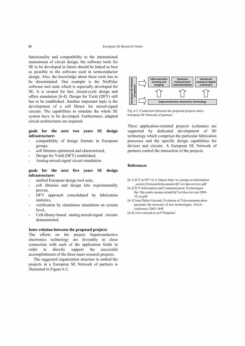
86 European SE Research Vision 8
functionality and compatibility to the international mainstream of circuit design, the software tools for SE to be developed in future should be linked as best as possible to the software used in semiconductor design. Also, the knowledge about these tools has to be disseminated. One example is the NioPulse software tool suite which is especially developed for SE. It is created for fast, closed-cycle design and offers simulation [6-4]. Design for Yield (DFY) still has to be established. Another important topic is the development of a cell library for mixed-signal circuits. The capabilities to simulate the whole SE system have to be developed. Furthermore, adapted circuit architectures are required. goals for the next two years SE design infrastructure: - compatibility of design formats in European
groups, - cell libraries optimized and characterized, - Design for Yield (DFY) established, - Analog-mixed-signal circuit simulation. goals for the next five years SE design infrastructure: - unified European design tool suite, - cell libraries and design kits experimentally
proven, - DFY approach consolidated by fabrication
statistics, - verification by simulation simulation on system
level, - Cell-library-based analog-mixed-signal circuits
demonstrated.
Inter-relation between the proposed projects The efforts on the project Superconductive electronics technology are favorably in close connection with each of the application fields in order to directly support the successful accomplishment of the three main research projects.
The suggested organization structure to embed the projects in a European SE Network of partners is illustrated in Figure 6-2.
Euro
pean
SE
Net
wor
k of
Ultra-sensitive sensing and
imaging
Quantum measurement
instrumentation
Advanced analog-to-digital
converters
Fig. 6-2. Connection between the proposed projects and a European SE Network of partners.
Three application-oriented projects (columns) are supported by dedicated development of SE technology which comprises the particular fabrication processes and the specific design capabilities for devices and circuits. A European SE Network of partners control the interaction of the projects.
References
[6-1] ICT in FP7 At A Glance http://ec.europa.eu/information
_society/tl/research/documents/fp7-ict-4poverview.pdf [6-2] ICT-Information and Communication Technologies
ftp://ftp.cordis.europa.eu/pub/fp7/ict/docs/ict-wp-2009-10_en.pdf
[6-3] Jean Didier Gayrard, Evolution of Telecommunication payloads: the necessity of new technologies. AIAA- conference 2002-1848
[6-4] www.niocad.co.za/#/Niopulse/
Superconductive electronics technology
part
ners

European Roadmap on Superconductor Electronics, Version June 2010 87
Acknowledgments
Gratefully acknowledge for fruitful and helpful discussions with D. Drung, L. Trahms, J. Beyer, PTB, Berlin, Germany, R. Behr, R. Dolata, M. Khabipov, O.F. Kieler, F. Müller, PTB, Braunschweig, Germany, S. Friedrich, LLNL, Livermore, USA, T. May, G. Zieger, IPHT, Jena, Germany, A. Ravex, Air Liquide, France, M. Maignan, Thales Alenia Space, France, T. Benschop, THALES, The Netherlands. N. Yoshikawa, Yokohama National University, Japan S. Hasuo, ISTEC/SRL, Japan S. Benz, NIST, Boulder, USA M. Nisenoff, Navy Research Laboratory (NRL) Washington, USA
87