evaluating and programming the 29k risc family third
TRANSCRIPT
Evaluating and Programming the29K RISC Family
Third Edition – DRAFT
A D V A N C E D M I C R O D E V I C E S

IF YOU HAVE QUESTIONS, WE’RE HERE TO HELP YOU.
Customer Service
AMD’s customer service network includes U.S. offices, international offices, anda customer training center. Expert technical assistance is available to answer 29KFamily hardware and software development questions from AMD’s worldwidestaff of field application engineers and factory support staff.
Hotline, Bulletin Board, and eMail Support
For answers to technical questions, AMD provides a toll-free number for directaccess to our engineering support staff. For overseas customers, the easiest way toreach the engineering support staff with your questions is via fax with a shortdescription of your question. Also available is the AMD bulletin board service,which provides the latest 29K product information, including technical informa-tion and data on upcoming product releases. AMD 29K Family customers alsoreceive technical support through electronic mail. This worldwide service is avail-able to 29K product users via the International UNIX eMail service. To access theservice, use the AMD eMail address: “[email protected].”
Engineering Support Staff:(800) 292-9263 ext. 2 toll free for U.S.(512) 602-4118 local for U.S.0800-89-1455 toll free for UK0031-11-1163 toll free for Japan(512) 602-5031 FAX for overseas
Bulletin Board:(800) 292-9263 ext. 1 toll free for U.S.(512) 602-4898 worldwide and local for U.S.
Documentation and Literature
The 29K Family Customer Support Group responds quickly to information andliterature requests. A simple phone call will get you free 29K Family informationsuch as data books, user’s manuals, data sheets, application notes, the Fusion29KPartner Solutions Catalog and Newsletter, and other literature. Internationally,contact your local AMD sales office for complete 29K Family literature.
Customer Support Group:(800) 292-9263 ext. 3 toll free for U.S.(512) 602-5651 local for U.S.(512) 602-5051 FAX for U.S.

Evaluating and Programming the 29K RISC Family
Third Edition – DRAFT
Daniel Mann
Advanced Micro Devices
� 1995 Daniel Mann
Advanced Micro Devices reserves the right to make changes in its productswithout notice in order to improve design or performance characteristics.
This publication neither states nor implies any warranty of any kind, including butnot limited to implied warrants of merchantability of fitness for a particular applica-tion. AMD assumes no responsibility for the use of any circuit other than the circuitin an AMD product.
The author and publisher of this book have used their best efforts in preparing thisbook. Although the information presented has been carefully reviewed and is be-lieved to be reliable, the author and publisher make no warranty of any kind, ex-pressed or implied, with regard to example programs or documentation contained inthis book. The author and publisher shall not be liable in any event for accidental orconsequential damages in connection with, or arising out of, the furnishing, perfor-mance, or use of these programs.
Trademarks
29K, Am29005, Am29027, Am29050, Am29030, Am29035, Am29040, Am29200,Am29205, Am29240, Am29243, Am29245, EZ030, SA29200, SA29240,SA29040, MiniMON29K, XRAY29K, ASM29K, ISS, SIM29, Scalable Clocking,Traceable Cache and UDI are a trademark of Advanced Micro Devices, Inc.Fusion29K is a registered service trademark of Advanced Micro Devices, Inc.AMD and Am29000 are registered trademarks of Advanced Micro Devices, Inc.PowerPC is a trademark of International Buisness Machines Corp.MRI and XRAY are trademarks of Microtec Reasearch Inc.High C is a registered trade mark of MetaWare Inc.i960 is a trademarks of Intel, Inc.MC68020 is a trademark of Motorola Inc.UNIX is a trademark of AT&T.NetROM is a trademark of XLNT Designs, Inc.UDB and UMON are trademarks of CaseTools Inc.Windows is a trademarks of Microsoft Corp.
Product names used in this publication are for identification purposes only and maybe trademarks of their respective companies.

To my wifeAudrey
and my sonGeoffrey

vii
Contents
Preface xxi. . . . . . . . . . . . . . . . . . . . . . . . . . . . . . . . . . . . . . . . . . . . . . . . . . . . .
Chapter 1Architectural Overview 1. . . . . . . . . . . . . . . . . . . . . . . . . . . . . . . . . . . 1.1 A RISC DEFINITION 3. . . . . . . . . . . . . . . . . . . . . . . . . . . . . . . . . . . . . . . . . . . . . 1.2 FAMILY MEMBER FEATURES 5. . . . . . . . . . . . . . . . . . . . . . . . . . . . . . . . . . . . 1.3 THE Am29000 3–BUS MICROPROCESSOR 7. . . . . . . . . . . . . . . . . . . . . . . .
1.3.1 The Am29005 11. . . . . . . . . . . . . . . . . . . . . . . . . . . . . . . . . . . . . . . . . . . . 1.4 THE Am29050 3–BUS FLOATING–POINT MICROPROCESSOR 11. . . . . . 1.5 THE Am29030 2–BUS MICROPROCESSOR 13. . . . . . . . . . . . . . . . . . . . . . . .
1.5.1 Am29030 Evaluation. 16. . . . . . . . . . . . . . . . . . . . . . . . . . . . . . . . . . . . . 1.5.2 The Am29035 16. . . . . . . . . . . . . . . . . . . . . . . . . . . . . . . . . . . . . . . . . . . .
1.6 THE Am29040 2–BUS MICROPROCESSOR 17. . . . . . . . . . . . . . . . . . . . . . . . 1.6.1 Am29040 Evaluation. 19. . . . . . . . . . . . . . . . . . . . . . . . . . . . . . . . . . . . .
1.7 A SUPERSCALAR 29K PROCESSOR 20. . . . . . . . . . . . . . . . . . . . . . . . . . . . . . 1.7.1 Instruction Issue and Data Dependency 21. . . . . . . . . . . . . . . . . . . . . 1.7.2 Reservation Stations 25. . . . . . . . . . . . . . . . . . . . . . . . . . . . . . . . . . . . . . 1.7.3 Register Renaming 27. . . . . . . . . . . . . . . . . . . . . . . . . . . . . . . . . . . . . . . 1.7.4 Branch Prediction 30. . . . . . . . . . . . . . . . . . . . . . . . . . . . . . . . . . . . . . . . .
1.8 THE Am29200 MICROCONTROLLER 33. . . . . . . . . . . . . . . . . . . . . . . . . . . . . . 1.8.1 ROM Region 35. . . . . . . . . . . . . . . . . . . . . . . . . . . . . . . . . . . . . . . . . . . . . 1.8.2 DRAM Region 36. . . . . . . . . . . . . . . . . . . . . . . . . . . . . . . . . . . . . . . . . . . . 1.8.3 Virtual DRAM Region 37. . . . . . . . . . . . . . . . . . . . . . . . . . . . . . . . . . . . . 1.8.4 PIA Region 37. . . . . . . . . . . . . . . . . . . . . . . . . . . . . . . . . . . . . . . . . . . . . . 1.8.5 DMA Controller 37. . . . . . . . . . . . . . . . . . . . . . . . . . . . . . . . . . . . . . . . . . . 1.8.6 16–bit I/O Port 38. . . . . . . . . . . . . . . . . . . . . . . . . . . . . . . . . . . . . . . . . . . 1.8.7 Parallel Port 38. . . . . . . . . . . . . . . . . . . . . . . . . . . . . . . . . . . . . . . . . . . . . 1.8.8 Serial Port 39. . . . . . . . . . . . . . . . . . . . . . . . . . . . . . . . . . . . . . . . . . . . . . .

viii Contents
1.8.9 I/O Video Interface 39. . . . . . . . . . . . . . . . . . . . . . . . . . . . . . . . . . . . . . . . 1.8.10 The SA29200 Evaluation Board 39. . . . . . . . . . . . . . . . . . . . . . . . . . . . 1.8.11 The Prototype Board 40. . . . . . . . . . . . . . . . . . . . . . . . . . . . . . . . . . . . . . 1.8.12 Am29200 Evaluation 40. . . . . . . . . . . . . . . . . . . . . . . . . . . . . . . . . . . . . 1.8.13 The Am29205 Microcontroller 40. . . . . . . . . . . . . . . . . . . . . . . . . . . . . .
1.9 THE Am29240 MICROCONTROLLER 41. . . . . . . . . . . . . . . . . . . . . . . . . . . . . . 1.9.1 The Am29243 Microcontroller 44. . . . . . . . . . . . . . . . . . . . . . . . . . . . . . 1.9.2 The Am29245 Microcontroller 44. . . . . . . . . . . . . . . . . . . . . . . . . . . . . . 1.9.3 The Am2924x Evaluation 45. . . . . . . . . . . . . . . . . . . . . . . . . . . . . . . . . .
1.10 REGISTER AND MEMORY SPACE 46. . . . . . . . . . . . . . . . . . . . . . . . . . . . . . . . 1.10.1 General Purpose Registers 47. . . . . . . . . . . . . . . . . . . . . . . . . . . . . . . . 1.10.2 Special Purpose Registers 49. . . . . . . . . . . . . . . . . . . . . . . . . . . . . . . . . 1.10.3 Translation Look–Aside Registers 61. . . . . . . . . . . . . . . . . . . . . . . . . . . 1.10.4 External Address Space 62. . . . . . . . . . . . . . . . . . . . . . . . . . . . . . . . . . .
1.11 INSTRUCTION FORMAT 64. . . . . . . . . . . . . . . . . . . . . . . . . . . . . . . . . . . . . . . . . 1.12 KEEPING THE RISC PIPELINE BUSY 65. . . . . . . . . . . . . . . . . . . . . . . . . . . . . 1.13 PIPELINE DEPENDENCIES 67. . . . . . . . . . . . . . . . . . . . . . . . . . . . . . . . . . . . . . 1.14 ARCHITECTURAL SIMULATION, sim29 70. . . . . . . . . . . . . . . . . . . . . . . . . . . .
1.14.1 The Simulation Event File 75. . . . . . . . . . . . . . . . . . . . . . . . . . . . . . . . . . 1.14.2 Analyzing the Simulation Log File 83. . . . . . . . . . . . . . . . . . . . . . . . . . .
Chapter 2Applications Programming 89. . . . . . . . . . . . . . . . . . . . . . . . . . . . . . . 2.1 C LANGUAGE PROGRAMMING 90. . . . . . . . . . . . . . . . . . . . . . . . . . . . . . . . . . .
2.1.1 Register Stack 91. . . . . . . . . . . . . . . . . . . . . . . . . . . . . . . . . . . . . . . . . . . 2.1.2 Activation Records 92. . . . . . . . . . . . . . . . . . . . . . . . . . . . . . . . . . . . . . . . 2.1.3 Spilling And Filling 93. . . . . . . . . . . . . . . . . . . . . . . . . . . . . . . . . . . . . . . . 2.1.4 Global Registers 94. . . . . . . . . . . . . . . . . . . . . . . . . . . . . . . . . . . . . . . . . . 2.1.5 Memory Stack 95. . . . . . . . . . . . . . . . . . . . . . . . . . . . . . . . . . . . . . . . . . . .
2.2 RUN–TIME HIF ENVIRONMENT 95. . . . . . . . . . . . . . . . . . . . . . . . . . . . . . . . . . 2.2.1 OS Preparations before Calling start In crt0 97. . . . . . . . . . . . . . . . . . 2.2.2 crt0 Preparations before Calling main() 100. . . . . . . . . . . . . . . . . . . . . . 2.2.3 Run–Time HIF Services 101. . . . . . . . . . . . . . . . . . . . . . . . . . . . . . . . . . . 2.2.4 Switching to Supervisor Mode 103. . . . . . . . . . . . . . . . . . . . . . . . . . . . . .
2.3 C LANGUAGE COMPILER 106. . . . . . . . . . . . . . . . . . . . . . . . . . . . . . . . . . . . . . . . 2.3.1 Compiler Optimizations 106. . . . . . . . . . . . . . . . . . . . . . . . . . . . . . . . . . . . 2.3.2 Metaware High C 29K Compiler 110. . . . . . . . . . . . . . . . . . . . . . . . . . . . 2.3.3 Free Software Foundation, GCC 112. . . . . . . . . . . . . . . . . . . . . . . . . . . . 2.3.4 C++ Compiler Selection 113. . . . . . . . . . . . . . . . . . . . . . . . . . . . . . . . . . . 2.3.5 Executable Code and Source Correspondence 113. . . . . . . . . . . . . . . 2.3.6 Linking Compiled Code 116. . . . . . . . . . . . . . . . . . . . . . . . . . . . . . . . . . . .
2.4 LIBRARY SUPPORT 119. . . . . . . . . . . . . . . . . . . . . . . . . . . . . . . . . . . . . . . . . . . . . 2.4.1 Memory Allocation 119. . . . . . . . . . . . . . . . . . . . . . . . . . . . . . . . . . . . . . . .

ixContents
2.4.2 Setjmp and Longjmp 120. . . . . . . . . . . . . . . . . . . . . . . . . . . . . . . . . . . . . . 2.4.3 Support Libraries 122. . . . . . . . . . . . . . . . . . . . . . . . . . . . . . . . . . . . . . . . .
2.5 C LANGUAGE INTERRUPT HANDLERS 123. . . . . . . . . . . . . . . . . . . . . . . . . . . 2.5.1 An Interrupt Context Cache with High C 29K 127. . . . . . . . . . . . . . . . . 2.5.2 An Interrupt Context Cache with GNU 128. . . . . . . . . . . . . . . . . . . . . . . 2.5.3 Using Signals to Deal with Interrupts 131. . . . . . . . . . . . . . . . . . . . . . . . 2.5.4 Interrupt Tag Words 134. . . . . . . . . . . . . . . . . . . . . . . . . . . . . . . . . . . . . . . 2.5.5 Overloaded INTR3 140. . . . . . . . . . . . . . . . . . . . . . . . . . . . . . . . . . . . . . . . 2.5.6 A Signal Dispatcher 143. . . . . . . . . . . . . . . . . . . . . . . . . . . . . . . . . . . . . . . 2.5.7 Minimizing Interrupt Latency 152. . . . . . . . . . . . . . . . . . . . . . . . . . . . . . . 2.5.8 Signal Processing Without a HIF Operating System 153. . . . . . . . . . . 2.5.9 An Example Am29200 Interrupt Handler 153. . . . . . . . . . . . . . . . . . . . .
2.6 SUPPORT UTILITY PROGRAMS 156. . . . . . . . . . . . . . . . . . . . . . . . . . . . . . . . . . 2.6.1 Examining Object Files (Type .o And a.Out) 156. . . . . . . . . . . . . . . . . . 2.6.2 Modifying Object Files 158. . . . . . . . . . . . . . . . . . . . . . . . . . . . . . . . . . . . . 2.6.3 Getting a Program into ROM 159. . . . . . . . . . . . . . . . . . . . . . . . . . . . . . .
Chapter 3Assembly Language Programming 161. . . . . . . . . . . . . . . . . . . . . . . . 3.1 INSTRUCTION SET 162. . . . . . . . . . . . . . . . . . . . . . . . . . . . . . . . . . . . . . . . . . . . . .
3.1.1 Integer Arithmetic 162. . . . . . . . . . . . . . . . . . . . . . . . . . . . . . . . . . . . . . . . . 3.1.2 Compare 164. . . . . . . . . . . . . . . . . . . . . . . . . . . . . . . . . . . . . . . . . . . . . . . . 3.1.3 Logical 165. . . . . . . . . . . . . . . . . . . . . . . . . . . . . . . . . . . . . . . . . . . . . . . . . . 3.1.4 Shift 165. . . . . . . . . . . . . . . . . . . . . . . . . . . . . . . . . . . . . . . . . . . . . . . . . . . . 3.1.5 Data Movement 168. . . . . . . . . . . . . . . . . . . . . . . . . . . . . . . . . . . . . . . . . . 3.1.6 Constant 172. . . . . . . . . . . . . . . . . . . . . . . . . . . . . . . . . . . . . . . . . . . . . . . . 3.1.7 Floating–point 173. . . . . . . . . . . . . . . . . . . . . . . . . . . . . . . . . . . . . . . . . . . . 3.1.8 Branch 173. . . . . . . . . . . . . . . . . . . . . . . . . . . . . . . . . . . . . . . . . . . . . . . . . . 3.1.9 Miscellaneous Instructions 175. . . . . . . . . . . . . . . . . . . . . . . . . . . . . . . . . 3.1.10 Reserved Instructions 176. . . . . . . . . . . . . . . . . . . . . . . . . . . . . . . . . . . . .
3.2 CODE OPTIMIZATION TECHNIQUES 177. . . . . . . . . . . . . . . . . . . . . . . . . . . . . . 3.3 AVAILABLE REGISTERS 178. . . . . . . . . . . . . . . . . . . . . . . . . . . . . . . . . . . . . . . . .
3.3.1 Useful Macro–Instructions 180. . . . . . . . . . . . . . . . . . . . . . . . . . . . . . . . . 3.3.2 Using Indirect Pointers and gr0 181. . . . . . . . . . . . . . . . . . . . . . . . . . . . . 3.3.3 Using gr1 182. . . . . . . . . . . . . . . . . . . . . . . . . . . . . . . . . . . . . . . . . . . . . . . . 3.3.4 Accessing Special Register Space 183. . . . . . . . . . . . . . . . . . . . . . . . . . 3.3.5 Floating–point Accumulators 184. . . . . . . . . . . . . . . . . . . . . . . . . . . . . . .
3.4 DELAYED EFFECTS OF INSTRUCTIONS 185. . . . . . . . . . . . . . . . . . . . . . . . . . 3.5 TRACE–BACK TAGS 186. . . . . . . . . . . . . . . . . . . . . . . . . . . . . . . . . . . . . . . . . . . . . 3.6 INTERRUPT TAGS 188. . . . . . . . . . . . . . . . . . . . . . . . . . . . . . . . . . . . . . . . . . . . . . 3.7 TRANSPARENT ROUTINES 190. . . . . . . . . . . . . . . . . . . . . . . . . . . . . . . . . . . . . . 3.8 INITIALIZING THE PROCESSOR 190. . . . . . . . . . . . . . . . . . . . . . . . . . . . . . . . . . 3.9 ASSEMBLER SYNTAX 191. . . . . . . . . . . . . . . . . . . . . . . . . . . . . . . . . . . . . . . . . . .

x Contents
3.9.1 The AMD Assembler 191. . . . . . . . . . . . . . . . . . . . . . . . . . . . . . . . . . . . . . 3.9.2 Free Software Foundation (GNU), Assembler 192. . . . . . . . . . . . . . . .
Chapter 4Interrupts and Traps 195. . . . . . . . . . . . . . . . . . . . . . . . . . . . . . . . . . . . . . 4.1 29K PROCESSOR FAMILY INTERRUPT SEQUENCE 196. . . . . . . . . . . . . . . . 4.2 29K PROCESSOR FAMILY INTERRUPT RETURN 197. . . . . . . . . . . . . . . . . . 4.3 SUPERVISOR MODE HANDLERS 199. . . . . . . . . . . . . . . . . . . . . . . . . . . . . . . . .
4.3.1 The Interrupt Environment 199. . . . . . . . . . . . . . . . . . . . . . . . . . . . . . . . . 4.3.2 Interrupt Latency 200. . . . . . . . . . . . . . . . . . . . . . . . . . . . . . . . . . . . . . . . . 4.3.3 Simple Freeze-mode Handlers 201. . . . . . . . . . . . . . . . . . . . . . . . . . . . . 4.3.4 Operating in Freeze mode 202. . . . . . . . . . . . . . . . . . . . . . . . . . . . . . . . . 4.3.5 Monitor mode 203. . . . . . . . . . . . . . . . . . . . . . . . . . . . . . . . . . . . . . . . . . . . 4.3.6 Freeze-mode Clock Interrupt Handler 204. . . . . . . . . . . . . . . . . . . . . . . 4.3.7 Removing Freeze mode 205. . . . . . . . . . . . . . . . . . . . . . . . . . . . . . . . . . . 4.3.8 Handling Nested Interrupts 208. . . . . . . . . . . . . . . . . . . . . . . . . . . . . . . . . 4.3.9 Saving Registers 210. . . . . . . . . . . . . . . . . . . . . . . . . . . . . . . . . . . . . . . . . 4.3.10 Enabling Interrupts 212. . . . . . . . . . . . . . . . . . . . . . . . . . . . . . . . . . . . . . . . 4.3.11 Restoring Saved Registers 214. . . . . . . . . . . . . . . . . . . . . . . . . . . . . . . . . 4.3.12 An Interrupt Queuing model 216. . . . . . . . . . . . . . . . . . . . . . . . . . . . . . . . 4.3.13 Making Timer Interrupts Synchronous 221. . . . . . . . . . . . . . . . . . . . . . .
4.4 USER-MODE INTERRUPT HANDLERS 222. . . . . . . . . . . . . . . . . . . . . . . . . . . . 4.4.1 Supervisor mode Code 223. . . . . . . . . . . . . . . . . . . . . . . . . . . . . . . . . . . . 4.4.2 Register Stack Operation 226. . . . . . . . . . . . . . . . . . . . . . . . . . . . . . . . . . 4.4.3 SPILL and FILL Trampoline 228. . . . . . . . . . . . . . . . . . . . . . . . . . . . . . . . 4.4.4 SPILL Handler 229. . . . . . . . . . . . . . . . . . . . . . . . . . . . . . . . . . . . . . . . . . . 4.4.5 FILL Handler 230. . . . . . . . . . . . . . . . . . . . . . . . . . . . . . . . . . . . . . . . . . . . . 4.4.6 Register File Inconsistencies 231. . . . . . . . . . . . . . . . . . . . . . . . . . . . . . . 4.4.7 Preparing the C Environment 234. . . . . . . . . . . . . . . . . . . . . . . . . . . . . . . 4.4.8 Handling Setjmp and Longjmp 236. . . . . . . . . . . . . . . . . . . . . . . . . . . . . .
Chapter 5Operating System Issues 239. . . . . . . . . . . . . . . . . . . . . . . . . . . . . . . . . 5.1 REGISTER CONTEXT 240. . . . . . . . . . . . . . . . . . . . . . . . . . . . . . . . . . . . . . . . . . . 5.2 SYNCHRONOUS CONTEXT SWITCH 242. . . . . . . . . . . . . . . . . . . . . . . . . . . . .
5.2.1 Optimizations 245. . . . . . . . . . . . . . . . . . . . . . . . . . . . . . . . . . . . . . . . . . . . 5.3 ASYNCHRONOUS CONTEXT SWITCH 249. . . . . . . . . . . . . . . . . . . . . . . . . . . . 5.4 INTERRUPTING USER MODE 250. . . . . . . . . . . . . . . . . . . . . . . . . . . . . . . . . . . .
5.4.1 Optimizations 253. . . . . . . . . . . . . . . . . . . . . . . . . . . . . . . . . . . . . . . . . . . . 5.5 PROCESSING SIGNALS IN USER MODE 254. . . . . . . . . . . . . . . . . . . . . . . . . . 5.6 INTERRUPTING SUPERVISOR MODE 258. . . . . . . . . . . . . . . . . . . . . . . . . . . . .
5.6.1 Optimizations 260. . . . . . . . . . . . . . . . . . . . . . . . . . . . . . . . . . . . . . . . . . . . 5.7 USER SYSTEM CALLS 261. . . . . . . . . . . . . . . . . . . . . . . . . . . . . . . . . . . . . . . . . . .

xiContents
5.8 FLOATING–POINT ISSUES 264. . . . . . . . . . . . . . . . . . . . . . . . . . . . . . . . . . . . . . . 5.9 DEBUGGER ISSUES 265. . . . . . . . . . . . . . . . . . . . . . . . . . . . . . . . . . . . . . . . . . . . 5.10 RESTORING CONTEXT 266. . . . . . . . . . . . . . . . . . . . . . . . . . . . . . . . . . . . . . . . . . 5.11 INTERRUPT LATENCY 268. . . . . . . . . . . . . . . . . . . . . . . . . . . . . . . . . . . . . . . . . . . 5.12 ON–CHIP CACHE SUPPORT 270. . . . . . . . . . . . . . . . . . . . . . . . . . . . . . . . . . . . . 5.13 INSTRUCTION CACHE MAINTENANCE 270. . . . . . . . . . . . . . . . . . . . . . . . . . .
5.13.1 Cache Locking and Invalidating 273. . . . . . . . . . . . . . . . . . . . . . . . . . . . . 5.13.2 Instruction Cache Coherence 275. . . . . . . . . . . . . . . . . . . . . . . . . . . . . . 5.13.3 Branch Target Cache 275. . . . . . . . . . . . . . . . . . . . . . . . . . . . . . . . . . . . . . 5.13.4 Am29030 2–bus Microprocessor 276. . . . . . . . . . . . . . . . . . . . . . . . . . . . 5.13.5 Am29240 and Am29040 Processors 277. . . . . . . . . . . . . . . . . . . . . . . .
5.14 DATA CACHE MAINTENANCE 277. . . . . . . . . . . . . . . . . . . . . . . . . . . . . . . . . . . . 5.14.1 Am29240 Microcontroller 279. . . . . . . . . . . . . . . . . . . . . . . . . . . . . . . . . . 5.14.2 Am29040 2–bus Microprocessor 283. . . . . . . . . . . . . . . . . . . . . . . . . . . . 5.14.3 Cache Locking and Invalidating 288. . . . . . . . . . . . . . . . . . . . . . . . . . . . . 5.14.4 Cache Consistency 288. . . . . . . . . . . . . . . . . . . . . . . . . . . . . . . . . . . . . . .
5.15 SELECTING AN OPERATING SYSTEM 290. . . . . . . . . . . . . . . . . . . . . . . . . . . . 5.16 SUMMARY 294. . . . . . . . . . . . . . . . . . . . . . . . . . . . . . . . . . . . . . . . . . . . . . . . . . . . . .
Chapter 6Memory Management Unit 295. . . . . . . . . . . . . . . . . . . . . . . . . . . . . . . . 6.1 SRAM VERSUS DRAM PERFORMANCE 296. . . . . . . . . . . . . . . . . . . . . . . . . . . 6.2 TRANSLATION LOOK–ASIDE BUFFER (TLB) OPERATION 300. . . . . . . . . .
6.2.1 Dual TLB Processors 305. . . . . . . . . . . . . . . . . . . . . . . . . . . . . . . . . . . . . 6.2.2 Taking a TLB Trap 307. . . . . . . . . . . . . . . . . . . . . . . . . . . . . . . . . . . . . . . .
6.3 PERFORMANCE EQUATION 308. . . . . . . . . . . . . . . . . . . . . . . . . . . . . . . . . . . . . 6.4 SOFTWARE CONTROLLED CACHE MEMORY ARCHITECTURE 310. . . . .
6.4.1 Cache Page Maintenance 313. . . . . . . . . . . . . . . . . . . . . . . . . . . . . . . . . 6.4.2 Data Access TLB Miss 315. . . . . . . . . . . . . . . . . . . . . . . . . . . . . . . . . . . . 6.4.3 Instruction Access TLB Miss 318. . . . . . . . . . . . . . . . . . . . . . . . . . . . . . . 6.4.4 Data Write TLB Protection 319. . . . . . . . . . . . . . . . . . . . . . . . . . . . . . . . . 6.4.5 Supervisor TLB Signal Handler 320. . . . . . . . . . . . . . . . . . . . . . . . . . . . . 6.4.6 Copying a Page into the Cache 322. . . . . . . . . . . . . . . . . . . . . . . . . . . . . 6.4.7 Copying a Page Out of the Cache 323. . . . . . . . . . . . . . . . . . . . . . . . . . 6.4.8 Cache Set Locked 325. . . . . . . . . . . . . . . . . . . . . . . . . . . . . . . . . . . . . . . . 6.4.9 Returning from Signal Handler 326. . . . . . . . . . . . . . . . . . . . . . . . . . . . . 6.4.10 Support Routines 327. . . . . . . . . . . . . . . . . . . . . . . . . . . . . . . . . . . . . . . . . 6.4.11 Performance Gain 328. . . . . . . . . . . . . . . . . . . . . . . . . . . . . . . . . . . . . . . .
Chapter 7Software Debugging 331. . . . . . . . . . . . . . . . . . . . . . . . . . . . . . . . . . . . . . 7.1 REGISTER ASSIGNMENT CONVENTION 331. . . . . . . . . . . . . . . . . . . . . . . . . . 7.2 PROCESSOR DEBUG SUPPORT 333. . . . . . . . . . . . . . . . . . . . . . . . . . . . . . . . .
xii Contents
7.2.1 Execution Mode 333. . . . . . . . . . . . . . . . . . . . . . . . . . . . . . . . . . . . . . . . . . 7.2.2 Memory Access Protection 334. . . . . . . . . . . . . . . . . . . . . . . . . . . . . . . . . 7.2.3 Trace Facility 334. . . . . . . . . . . . . . . . . . . . . . . . . . . . . . . . . . . . . . . . . . . . . 7.2.4 Program Counter register PC2 335. . . . . . . . . . . . . . . . . . . . . . . . . . . . . 7.2.5 Monitor Mode 336. . . . . . . . . . . . . . . . . . . . . . . . . . . . . . . . . . . . . . . . . . . . 7.2.6 Instruction Breakpoints 336. . . . . . . . . . . . . . . . . . . . . . . . . . . . . . . . . . . . 7.2.7 Data Breakpoints 338. . . . . . . . . . . . . . . . . . . . . . . . . . . . . . . . . . . . . . . . .
7.3 THE MiniMON29K DEBUGGER 338. . . . . . . . . . . . . . . . . . . . . . . . . . . . . . . . . . . 7.3.1 The Target MiniMON29K Component 339. . . . . . . . . . . . . . . . . . . . . . . 7.3.2 Register Usage 340. . . . . . . . . . . . . . . . . . . . . . . . . . . . . . . . . . . . . . . . . . . 7.3.3 The DebugCore 341. . . . . . . . . . . . . . . . . . . . . . . . . . . . . . . . . . . . . . . . . . 7.3.4 DebugCore installation 342. . . . . . . . . . . . . . . . . . . . . . . . . . . . . . . . . . . . 7.3.5 Advanced DBG and CFG Module Features 347. . . . . . . . . . . . . . . . . . 7.3.6 The Message System 348. . . . . . . . . . . . . . . . . . . . . . . . . . . . . . . . . . . . . 7.3.7 MSG Operation 349. . . . . . . . . . . . . . . . . . . . . . . . . . . . . . . . . . . . . . . . . . 7.3.8 MSG Virtual Interrupt Mechanism 349. . . . . . . . . . . . . . . . . . . . . . . . . . .
7.4 THE OS–BOOT OPERATING SYSTEM 350. . . . . . . . . . . . . . . . . . . . . . . . . . . . . 7.4.1 Register Usage 351. . . . . . . . . . . . . . . . . . . . . . . . . . . . . . . . . . . . . . . . . . . 7.4.2 OS–boot Operation 351. . . . . . . . . . . . . . . . . . . . . . . . . . . . . . . . . . . . . . . 7.4.3 HIF Services 352. . . . . . . . . . . . . . . . . . . . . . . . . . . . . . . . . . . . . . . . . . . . . 7.4.4 Adding New Device Drivers 353. . . . . . . . . . . . . . . . . . . . . . . . . . . . . . . . 7.4.5 Memory Access Protection 354. . . . . . . . . . . . . . . . . . . . . . . . . . . . . . . . . 7.4.6 Down Loading a New OS 358. . . . . . . . . . . . . . . . . . . . . . . . . . . . . . . . . .
7.5 UNIVERSAL DEBUG INTERFACE (UDI) 359. . . . . . . . . . . . . . . . . . . . . . . . . . . . 7.5.1 Debug Tool Developers 360. . . . . . . . . . . . . . . . . . . . . . . . . . . . . . . . . . . . 7.5.2 UDI Specification 361. . . . . . . . . . . . . . . . . . . . . . . . . . . . . . . . . . . . . . . . . 7.5.3 P–trace 363. . . . . . . . . . . . . . . . . . . . . . . . . . . . . . . . . . . . . . . . . . . . . . . . . 7.5.4 The GDB–UDI Connection 364. . . . . . . . . . . . . . . . . . . . . . . . . . . . . . . . . 7.5.5 The UDI–MiniMON29K Monitor Connection, MonTIP 365. . . . . . . . . . 7.5.6 The MiniMON29K User–Interface, MonDFE 366. . . . . . . . . . . . . . . . . 7.5.7 The UDI – Instruction Set Simulator Connection, ISSTIP 368. . . . . . 7.5.8 UDI Benefits 369. . . . . . . . . . . . . . . . . . . . . . . . . . . . . . . . . . . . . . . . . . . . . 7.5.9 Getting Started with GDB 370. . . . . . . . . . . . . . . . . . . . . . . . . . . . . . . . . . 7.5.10 GDB and MiniMON29K Summary 373. . . . . . . . . . . . . . . . . . . . . . . . . . .
7.6 SIMPLIFYING ASSEMBLY CODE DEBUG 374. . . . . . . . . . . . . . . . . . . . . . . . . . 7.7 SOURCE LEVEL DEBUGGING USING A WINDOW INTERFACE 377. . . . . . 7.8 TRACING PROGRAM EXECUTION 383. . . . . . . . . . . . . . . . . . . . . . . . . . . . . . . . 7.9 Fusion3D TOOLS 397. . . . . . . . . . . . . . . . . . . . . . . . . . . . . . . . . . . . . . . . . . . . . . . .
7.9.1 NetROM ROM Emulator 397. . . . . . . . . . . . . . . . . . . . . . . . . . . . . . . . . . . 7.9.2 HP16500B Logic Analyzer 400. . . . . . . . . . . . . . . . . . . . . . . . . . . . . . . . . 7.9.3 Selecting Trace Signals 404. . . . . . . . . . . . . . . . . . . . . . . . . . . . . . . . . . . 7.9.4 Corelis PI – Am29040 Preprocessor 406. . . . . . . . . . . . . . . . . . . . . . . . 7.9.5 Corelis PI – Am29460 Preprocessor 408. . . . . . . . . . . . . . . . . . . . . . . .

xiiiContents
Chapter 8Selecting a Processor 418. . . . . . . . . . . . . . . . . . . . . . . . . . . . . . . . . . . . 8.1 THE 29K FAMILY 419. . . . . . . . . . . . . . . . . . . . . . . . . . . . . . . . . . . . . . . . . . . . . . . .
8.1.1 Selecting a Microcontroller 423. . . . . . . . . . . . . . . . . . . . . . . . . . . . . . . . . 8.1.2 Moving up to an Am2920x Microcontroller 431. . . . . . . . . . . . . . . . . . . 8.1.3 Selecting a Microprocessor 434. . . . . . . . . . . . . . . . . . . . . . . . . . . . . . . . 8.1.4 Reducing the Register Window Size 443. . . . . . . . . . . . . . . . . . . . . . . .
Appendix AHIF Service Calls 450. . . . . . . . . . . . . . . . . . . . . . . . . . . . . . . . . . . . . . . . .
A.1 Service Call Numbers And Parameters 450. . . . . . . . . . . . . . . . . . . . . . A.2 Error Numbers 505. . . . . . . . . . . . . . . . . . . . . . . . . . . . . . . . . . . . . . . . . . .
Appendix BHIF Signal Processing 512. . . . . . . . . . . . . . . . . . . . . . . . . . . . . . . . . . . .
B.1 User Trampoline Code 512. . . . . . . . . . . . . . . . . . . . . . . . . . . . . . . . . . . . B.2 Library Glue Routines to HIF Signal Services 518. . . . . . . . . . . . . . . . . B.3 The Library signal() Routine for Registering a Handler 519. . . . . . . . .
Appendix CSoftware Assigned Trap Numbers 522. . . . . . . . . . . . . . . . . . . . . . . . .
Appendix DDebugCore 2.0 Specification 526. . . . . . . . . . . . . . . . . . . . . . . . . . . . . . D.1 INTRODUCTION 526. . . . . . . . . . . . . . . . . . . . . . . . . . . . . . . . . . . . . . . . . . . . . . . . D.2 REGISTER USAGE 527. . . . . . . . . . . . . . . . . . . . . . . . . . . . . . . . . . . . . . . . . . . . . . D.3 DEBUGCORE 1.0 ENHANCEMENTS 527. . . . . . . . . . . . . . . . . . . . . . . . . . . . . .
D.3.1 Executing OS Service Functions 528. . . . . . . . . . . . . . . . . . . . . . . . . . . . D.3.2 Per–Process Breakpoints 529. . . . . . . . . . . . . . . . . . . . . . . . . . . . . . . . . . D.3.3 Current PID 530. . . . . . . . . . . . . . . . . . . . . . . . . . . . . . . . . . . . . . . . . . . . . . D.3.4 Virtual or Physical Breakpoints 530. . . . . . . . . . . . . . . . . . . . . . . . . . . . . D.3.5 Breakpoint Functions 531. . . . . . . . . . . . . . . . . . . . . . . . . . . . . . . . . . . . . .
D.4 MODULE INTERCONNECTION 531. . . . . . . . . . . . . . . . . . . . . . . . . . . . . . . . . . . D.4.1 The DebugCore 2.0 531. . . . . . . . . . . . . . . . . . . . . . . . . . . . . . . . . . . . . . . D.4.2 The Message System 1.0 536. . . . . . . . . . . . . . . . . . . . . . . . . . . . . . . . . . D.4.3 The DebugCore 2.0 Configuration 539. . . . . . . . . . . . . . . . . . . . . . . . . .
References and Bibliography 542. . . . . . . . . . . . . . . . . . . . . . . . . . . . . . . .
Index 544. . . . . . . . . . . . . . . . . . . . . . . . . . . . . . . . . . . . . . . . . . . . . . . . . . . . . . .

xiv Contents

xv
Figures
Figure 1-1. RISC Pipeline 3. . . . . . . . . . . . . . . . . . . . . . . . . . . . . . . . . . . . . . . . . . . . . . . . . . .
Figure 1-2. CISC Pipeline 4. . . . . . . . . . . . . . . . . . . . . . . . . . . . . . . . . . . . . . . . . . . . . . . . . .
Figure 1-3. Processor Price–Performance Summary 6. . . . . . . . . . . . . . . . . . . . . . . . . . . . . .
Figure 1-4. Am29000 Processor 3–bus Harvard Memory System 9. . . . . . . . . . . . . . . . . . . .
Figure 1-5. The Instruction Window for Out–of–Order Instruction Issue 24. . . . . . . . . . . . . .
Figure 1-6. A Function Unit with Reservation Stations 26. . . . . . . . . . . . . . . . . . . . . . . . . . . .
Figure 1-7. Register Dependency Resolved by Register Renaming 28. . . . . . . . . . . . . . . . . . .
Figure 1-8. Circular Reorder Buffer Format 28. . . . . . . . . . . . . . . . . . . . . . . . . . . . . . . . . . . .
Figure 1-9. Multiple Function Units with a Reorder Buffer 29. . . . . . . . . . . . . . . . . . . . . . . . .
Figure 1-10. Instruction Decode with No Branch Prediction 31. . . . . . . . . . . . . . . . . . . . . . . .
Figure 1-11. Four–Instruction Decoder with Branch Prediction 32. . . . . . . . . . . . . . . . . . . . .
Figure 1-12. Am29200 Microcontroller Address Space Regions 35. . . . . . . . . . . . . . . . . . . . .
Figure 1-13. Am29200 Microcontroller Block Diagram 36. . . . . . . . . . . . . . . . . . . . . . . . . . .
Figure 1-14. General Purpose Register Space 48. . . . . . . . . . . . . . . . . . . . . . . . . . . . . . . . . . .
Figure 1-15. Special Purpose Register Space for the Am29000 Microprocessor 51. . . . . . . .
Figure 1-16. Am29000 Processor Program Counter 55. . . . . . . . . . . . . . . . . . . . . . . . . . . . . .
Figure 1-17. Additional Special Purpose Registers for the Monitor Mode Support 56. . . . . .
Figure 1-18. Additional Special Purpose Registers for the Am29050 Microprocessor 57. . .
Figure 1-19. Additional Special Purpose Registers for Breakpoint Control 57. . . . . . . . . . . .
Figure 1-20. Additional Special Purpose Registers for On–Chip Cache Control 58. . . . . . . .
Figure 1-21. Additional Special Purpose Register for the Am29050 Microprocessor 61. . . . .
Figure 1-22. Instruction Format 64. . . . . . . . . . . . . . . . . . . . . . . . . . . . . . . . . . . . . . . . . . . . . . .
Figure 1-23. Frequently Occurring Instruction–Field Uses 66. . . . . . . . . . . . . . . . . . . . . . . . . .
Figure 1-24. Pipeline Stages for BTC Miss 68. . . . . . . . . . . . . . . . . . . . . . . . . . . . . . . . . . . . .

xvi Figures
Figure 1-25. Pipeline Stages for a BTC Hit 69. . . . . . . . . . . . . . . . . . . . . . . . . . . . . . . . . . . . .
Figure 1-26. Data Forwarding and Bad–Load Scheduling 69. . . . . . . . . . . . . . . . . . . . . . . . .
Figure 1-27. Register Initialization Performed by sim29 74. . . . . . . . . . . . . . . . . . . . . . . . . . .
Figure 2-1. Cache Window 92. . . . . . . . . . . . . . . . . . . . . . . . . . . . . . . . . . . . . . . . . . . . . . . . . .
Figure 2-2. Overlapping Activation Record Registers 94. . . . . . . . . . . . . . . . . . . . . . . . . . . . .
Figure 2-3. 29K Microcontroller Interrupt Control Register 141. . . . . . . . . . . . . . . . . . . . . . . .
Figure 2-4. Processing Interrupts with a Signal Dispatcher 146. . . . . . . . . . . . . . . . . . . . . . . .
Figure 3-1. The EXTRACT Instruction uses the Funnel Shifter 166. . . . . . . . . . . . . . . . . . . . .
Figure 3-2. LOAD and STORE Instruction Format 170. . . . . . . . . . . . . . . . . . . . . . . . . . . . . . .
Figure 3-3. General Purpose Register Usage 179. . . . . . . . . . . . . . . . . . . . . . . . . . . . . . . . . . .
Figure 3-4. Global Register gr1 Fields 182. . . . . . . . . . . . . . . . . . . . . . . . . . . . . . . . . . . . . . . .
Figure 3-5. Trace–Back Tag Format 187. . . . . . . . . . . . . . . . . . . . . . . . . . . . . . . . . . . . . . . . . .
Figure 3-6. Walking Back Through Activation Records 188. . . . . . . . . . . . . . . . . . . . . . . . . . . .
Figure 3-7. Interrupt Procedure Tag Words 189. . . . . . . . . . . . . . . . . . . . . . . . . . . . . . . . . . . . .
Figure 4-1. Interrupt Handler Execution Stages 196. . . . . . . . . . . . . . . . . . . . . . . . . . . . . . . . .
Figure 4-2. The Format of Special Registers CPS and OPS 197. . . . . . . . . . . . . . . . . . . . . . . .
Figure 4-3. Interrupted Load Multiple Instruction 209. . . . . . . . . . . . . . . . . . . . . . . . . . . . . . .
Figure 4-4. Am29000 Processor Interrupt Enable Logic 213. . . . . . . . . . . . . . . . . . . . . . . . . .
Figure 4-5. Interrupt Queue Entry Chaining 216. . . . . . . . . . . . . . . . . . . . . . . . . . . . . . . . . . . .
Figure 4-6. An Interrupt Queuing Approach 218. . . . . . . . . . . . . . . . . . . . . . . . . . . . . . . . . . . .
Figure 4-7. Queued Interrupt Execution Flow 220. . . . . . . . . . . . . . . . . . . . . . . . . . . . . . . . . . .
Figure 4-8. Saved Registers 224. . . . . . . . . . . . . . . . . . . . . . . . . . . . . . . . . . . . . . . . . . . . . . . . .
Figure 4-9. Register and Stack Cache 227. . . . . . . . . . . . . . . . . . . . . . . . . . . . . . . . . . . . . . . . .
Figure 4-10. Stack Upon Interrupt 231. . . . . . . . . . . . . . . . . . . . . . . . . . . . . . . . . . . . . . . . . . . .
Figure 4-11. Stack After Fix–up 235. . . . . . . . . . . . . . . . . . . . . . . . . . . . . . . . . . . . . . . . . . . . . .
Figure 4-12. Long–Jump to Setjmp 237. . . . . . . . . . . . . . . . . . . . . . . . . . . . . . . . . . . . . . . . . . . .
Figure 5-1. A Consistent Register Stack Cache 241. . . . . . . . . . . . . . . . . . . . . . . . . . . . . . . . . .
Figure 5-2. Current Procedures Activation Record 242. . . . . . . . . . . . . . . . . . . . . . . . . . . . . . .
Figure 5-3. Overlapping Activation Records Eventual Spill Out of the Register Stack Cache 247. . . . . . . . . . . . . . . . . . . . . . . . . . . . . . . . . . . . . . . . . . . .
Figure 5-4. Context Save PCB Layout 248. . . . . . . . . . . . . . . . . . . . . . . . . . . . . . . . . . . . . . . .
Figure 5-5. Register Stack Cut–Across 263. . . . . . . . . . . . . . . . . . . . . . . . . . . . . . . . . . . . . . . . .
Figure 5-6. Instruction Cache Tag and Status bits 272. . . . . . . . . . . . . . . . . . . . . . . . . . . . . . . .
Figure 5-7. Am29240 Microcontroller Cache Data Flow 281. . . . . . . . . . . . . . . . . . . . . . . . . .
Figure 5-8. Am29240 Data Cache Tag and Status bits 281. . . . . . . . . . . . . . . . . . . . . . . . . . . .
Figure 5-9. Am29040 2–bus Microprocessor Cache Data Flow 284. . . . . . . . . . . . . . . . . . . . .
xviiFigures
Figure 5-10. Am29040 Data Cache Tag and Status bits 285. . . . . . . . . . . . . . . . . . . . . . . . . . .
Figure 6-1. Average Cycles per Instruction Using DRAM 297. . . . . . . . . . . . . . . . . . . . . . . . . .
Figure 6-2. Average Cycles per Instruction Using SRAM 298. . . . . . . . . . . . . . . . . . . . . . . . . . .
Figure 6-3. Block Diagram of Example Joint I/D System 299. . . . . . . . . . . . . . . . . . . . . . . . . .
Figure 6-4. Average Cycles per Instruction 300. . . . . . . . . . . . . . . . . . . . . . . . . . . . . . . . . . . . .
Figure 6-5. Probability of a TLB Access per Instruction 301. . . . . . . . . . . . . . . . . . . . . . . . . . .
Figure 6-6. TLB Field Composition for 4K Byte Page Size 302. . . . . . . . . . . . . . . . . . . . . . . . .
Figure 6-7. Block Diagram of Am29000 processor TLB Layout 303. . . . . . . . . . . . . . . . . . . . .
Figure 6-8. Am29000 Processor TLB Register Format 304. . . . . . . . . . . . . . . . . . . . . . . . . . . .
Figure 6-9. TLB Register Format for Processor with Two TLBs 306. . . . . . . . . . . . . . . . . . . . .
Figure 6-10. TLB Miss Ratio for Joint I/D 2–1 SRAM System 309. . . . . . . . . . . . . . . . . . . . . . .
Figure 6-11. Average Cycles Required per TLB Miss 310. . . . . . . . . . . . . . . . . . . . . . . . . . . . . .
Figure 6-12. PTE Mapping to Cache Real Page Numbers 312. . . . . . . . . . . . . . . . . . . . . . . . . .
Figure 6-13. Software Controlled Cache, K bytes paged–in 314. . . . . . . . . . . . . . . . . . . . . . . .
Figure 6-14. Probability of a Page–in Given a TLB Miss 314. . . . . . . . . . . . . . . . . . . . . . . . . .
Figure 6-15. TLB Signal Frame 318. . . . . . . . . . . . . . . . . . . . . . . . . . . . . . . . . . . . . . . . . . . . . .
Figure 6-16. Cache Performance Gains with the Assembly Utility 328. . . . . . . . . . . . . . . . . . .
Figure 6-17. Cache Performance Gains with NROFF Utility 329. . . . . . . . . . . . . . . . . . . . . . .
Figure 6-18. Comparing Cache Based Systems with DRAM Only Systems 329. . . . . . . . . . . . .
Figure 7-1. 29K Development and Debug Tools 332. . . . . . . . . . . . . . . . . . . . . . . . . . . . . . . . .
Figure 7-2. MinMON29k Debugger Components 338. . . . . . . . . . . . . . . . . . . . . . . . . . . . . . . .
Figure 7-3. 29K Target Software Module Configuration 340. . . . . . . . . . . . . . . . . . . . . . . . . . .
Figure 7-4. Vector Table Assignment for DebugCore 2.0 343. . . . . . . . . . . . . . . . . . . . . . . . . . .
Figure 7-5. Processor Initialization Code Sequence 344. . . . . . . . . . . . . . . . . . . . . . . . . . . . . .
Figure 7-6. Operating System Information Passed to dbg_control() 345. . . . . . . . . . . . . . . . . .
Figure 7-7. Return Structure from dbg_control() 346. . . . . . . . . . . . . . . . . . . . . . . . . . . . . . . . .
Figure 7-8. Typical OS–boot Memory Layout 355. . . . . . . . . . . . . . . . . . . . . . . . . . . . . . . . . . .
Figure 7-9. Currently Available Debugging Tools that Conform to UDI Specification 362. . . .
Figure 7-10. The UDB to 29K Connection via the GIO Process 378. . . . . . . . . . . . . . . . . . . . .
Figure 7-11. UDB Main Window Showing Source Code 380. . . . . . . . . . . . . . . . . . . . . . . . . . .
Figure 7-12. UDB Window Showing the Assembly Code Associated with the Previous Source Code Window 382. . . . . . . . . . . . . . . . . . . . . . . . . . . . . . . . . . . . .
Figure 7-13. UDB Window Showing Global Registers 384. . . . . . . . . . . . . . . . . . . . . . . . . . . . . .
Figure 7-14. HP16500B Logic Analyzer Window Showing State Listing 386. . . . . . . . . . . . . . . .
Figure 7-15. Path Taken By Am29040 Recursive Trace Processing Algorithm 390. . . . . . . . . . .
Figure 7-16. UDB Console Window Showing Processed Trace Information 395. . . . . . . . . . . . .
xviii Figures
Figure 7-17. UDB Trace Window Showing Processed Trace Information 396. . . . . . . . . . . . . .
Figure 7-18. PI–Am29460 Preprocessor Trace Capture Scheme 409. . . . . . . . . . . . . . . . . . . . .
Figure 7-19. PI–Am29460 Preprocessor Trace Capture Timing 410. . . . . . . . . . . . . . . . . . . . .
Figure 7-20. Slave Data Supporting Am29460 Traceable Cache 412. . . . . . . . . . . . . . . . . . . .
Figure 7-21. RLE Output Queue From Reorder Buffer 412. . . . . . . . . . . . . . . . . . . . . . . . . . . .
Figure 8-1. 29K Microcontrollers Running the LAPD BenchmarkWith 16 MHz Memory Systems 424. . . . . . . . . . . . . . . . . . . . . . . . . . . . . . . . . . . . .
Figure 8-2. 29K Microcontrollers Running the LAPD BenchmarkWith 20 MHz Memory Systems 428. . . . . . . . . . . . . . . . . . . . . . . . . . . . . . . . . . . . .
Figure 8-3. 29K Microcontrollers Running the LAPD BenchmarkWith 25 MHz Memory Systems 430. . . . . . . . . . . . . . . . . . . . . . . . . . . . . . . . . . . . .
Figure 8-4. 29K Microcontrollers Running the LAPD BenchmarkWith 33 MHz Memory Systems 431. . . . . . . . . . . . . . . . . . . . . . . . . . . . . . . . . . . . .
Figure 8-5. Am2920x Microcontrollers Running the LAPD Benchmark with 8–bit and 16–bit Memory Systems Operating at 12 and 16 MHz 432. . . . . . . . . . .
Figure 8-6. 29K Microprocessors Running the LAPD Benchmarkwith 16 MHz Memory systems 437. . . . . . . . . . . . . . . . . . . . . . . . . . . . . . . . . . . . .
Figure 8-7. 29K Microprocessors Running the LAPD Benchmarkwith 20 MHz Memory Systems 439. . . . . . . . . . . . . . . . . . . . . . . . . . . . . . . . . . . . .
Figure 8-8. 29K Microprocessors Running the LAPD Benchmarkwith 25 MHz Memory Systems 440. . . . . . . . . . . . . . . . . . . . . . . . . . . . . . . . . . . . .
Figure 8-9. 29K Microprocessors Running the LAPD Benchmarkwith 33 MHz Memory Systems 442. . . . . . . . . . . . . . . . . . . . . . . . . . . . . . . . . . . . .
Figure 8-10. Am29040 Microprocessors Running the LAPD Benchmarkwith Various Register Stack Window Sizes 443. . . . . . . . . . . . . . . . . . . . . . . . . . . .
Figure 8-11. Am29200 Microcontroller Running the LAPD Benchmarkwith Various Register Stack Window Sizes 444. . . . . . . . . . . . . . . . . . . . . . . . . . . .
Figure 8-12. Am29040 Microprocessors Running the Stanford Benchmarkwith Various Register Stack Window Sizes 445. . . . . . . . . . . . . . . . . . . . . . . . . . . .
Figure 8-13. Reduction In Worst–Case Asynchronous Task Context Switch Timeswith Various Register Stack Window Sizes 447. . . . . . . . . . . . . . . . . . . . . . . . . . . .
Figure A-1. HIF Register Preservation for Signals 497. . . . . . . . . . . . . . . . . . . . . . . . . . . . . . . .
Figure D-1. 29K Target Software Module configuration 527. . . . . . . . . . . . . . . . . . . . . . . . . . .
Figure D-2. Data Structure Shared by Operating System and DebugCore 2.0 529. . . . . . . . . .
Figure D-3. DebugCore 2.0 Module 532. . . . . . . . . . . . . . . . . . . . . . . . . . . . . . . . . . . . . . . . . . .
Figure D-4. OS Information Passed to dbg_control() 533. . . . . . . . . . . . . . . . . . . . . . . . . . . . .
Figure D-5. Return Structure from dbg_control() 533. . . . . . . . . . . . . . . . . . . . . . . . . . . . . . . .
Figure D-6. DebugCore 2.0 Receive Messages 537. . . . . . . . . . . . . . . . . . . . . . . . . . . . . . . . . .
Figure D-7. Message System 1.0 Module 537. . . . . . . . . . . . . . . . . . . . . . . . . . . . . . . . . . . . . . .
Figure D-8. Configuration Module 539. . . . . . . . . . . . . . . . . . . . . . . . . . . . . . . . . . . . . . . . . . . .

xix
Tables
Table 1-1. Pin Compatible 3–bus 29K Family Processors 8. . . . . . . . . . . . . . . . . . . . . . . . .
Table 1-2. Pin Compatible 2–bus 29K Family Processors 14. . . . . . . . . . . . . . . . . . . . . . . . .
Table 1-3. Am2920x Microcontroller Members of 29K Processor Family 34. . . . . . . . . . . . . .
Table 1-4. Am2924x Microcontroller Members of 29K Processor Family 42. . . . . . . . . . . . . .
Table 1-5. 3–bus Processor Memory Modeling Parameters for sim29 76. . . . . . . . . . . . . . . .
Table 1-6. 3–bus Processor DRAM Modeling Parameters for sim29 (continued) 77. . . . . . . .
Table 1-7. 3–bus Processor Static Column Modeling Parameters for sim29 (continued) 77. .
Table 1-8. 3–bus Processor Memory Modeling Parameters for sim29 (continued) 78. . . . . . .
Table 1-9. 2–bus Processor Memory Modeling Parameters for older sim29 78. . . . . . . . . . . .
Table 1-10. 2–bus Processor Memory Modeling Parameters for newer sim29 79. . . . . . . . . .
Table 1-11. Microcontroller Memory Modeling Parameters for sim29 81. . . . . . . . . . . . . . . .
Table 1-12. Microcontroller Processor Memory Modeling Parameters for newer sim29 83. .
Table 2-1. Trap Handler Vectors 99. . . . . . . . . . . . . . . . . . . . . . . . . . . . . . . . . . . . . . . . . . . . . .
Table 2-2. HIF Service Calls 102. . . . . . . . . . . . . . . . . . . . . . . . . . . . . . . . . . . . . . . . . . . . . . . . .
Table 2-3. HIF Service Call Parameters 104. . . . . . . . . . . . . . . . . . . . . . . . . . . . . . . . . . . . . . .
Table 2-4. HIF Service Call Parameters (Concluded) 105. . . . . . . . . . . . . . . . . . . . . . . . . . . . .
Table 3-1. Integer Arithmetic Instructions 163. . . . . . . . . . . . . . . . . . . . . . . . . . . . . . . . . . . . . .
Table 3-2. Integer Arithmetic Instructions (Concluded) 164. . . . . . . . . . . . . . . . . . . . . . . . . . . .
Table 3-3. Compare Instructions 166. . . . . . . . . . . . . . . . . . . . . . . . . . . . . . . . . . . . . . . . . . . . . .
Table 3-4. Compare Instructions (Concluded) 167. . . . . . . . . . . . . . . . . . . . . . . . . . . . . . . . . . .
Table 3-5. Logical Instructions 168. . . . . . . . . . . . . . . . . . . . . . . . . . . . . . . . . . . . . . . . . . . . . . .
Table 3-6. Shift Instructions 168. . . . . . . . . . . . . . . . . . . . . . . . . . . . . . . . . . . . . . . . . . . . . . . . .
Table 3-7. Data Move Instructions 169. . . . . . . . . . . . . . . . . . . . . . . . . . . . . . . . . . . . . . . . . . . .
Table 3-8. Data Move Instructions (Concluded) 170. . . . . . . . . . . . . . . . . . . . . . . . . . . . . . . . .

xx Tables
Table 3-9. Constant Instructions 172. . . . . . . . . . . . . . . . . . . . . . . . . . . . . . . . . . . . . . . . . . . . . .
Table 3-10. Floating–Point Instructions 174. . . . . . . . . . . . . . . . . . . . . . . . . . . . . . . . . . . . . . . .
Table 3-11. Floating–Point Instructions (Concluded) 175. . . . . . . . . . . . . . . . . . . . . . . . . . . . .
Table 3-12. Branch Instructions 176. . . . . . . . . . . . . . . . . . . . . . . . . . . . . . . . . . . . . . . . . . . . . .
Table 3-13. Miscellaneous Instructions 177. . . . . . . . . . . . . . . . . . . . . . . . . . . . . . . . . . . . . . . .
Table 4-1. Global Register Allocations 199. . . . . . . . . . . . . . . . . . . . . . . . . . . . . . . . . . . . . . . . .
Table 4-2. Expanded Register Usage 223. . . . . . . . . . . . . . . . . . . . . . . . . . . . . . . . . . . . . . . . . .
Table 5-1. 29K Family Instruction and Date Cache Support 271. . . . . . . . . . . . . . . . . . . . . . . .
Table 5-2. Instruction Cache Comparison 273. . . . . . . . . . . . . . . . . . . . . . . . . . . . . . . . . . . . . .
Table 5-3. Data Cache Comparison 280. . . . . . . . . . . . . . . . . . . . . . . . . . . . . . . . . . . . . . . . . . .
Table 5-4. PGM Field of the Am29040 Microprocessor TLB 286. . . . . . . . . . . . . . . . . . . . . . . .
Table 6-1. PGM Field of the Am29040 Microprocessor TLB 307. . . . . . . . . . . . . . . . . . . . . . . .
Table 7-1. 29K Family On-chip Debug Support 337. . . . . . . . . . . . . . . . . . . . . . . . . . . . . . . . . .
Table 7-2. UDI–p Procedures (Version 1.2) 363. . . . . . . . . . . . . . . . . . . . . . . . . . . . . . . . . . . . .
Table 7-3. ptrace() Services 364. . . . . . . . . . . . . . . . . . . . . . . . . . . . . . . . . . . . . . . . . . . . . . . . .
Table 7-4. GDB Remote–Target Operations 365. . . . . . . . . . . . . . . . . . . . . . . . . . . . . . . . . . . . .
Table 7-5. PI–Am29040 Logic Analyzer Pod Assignment 407. . . . . . . . . . . . . . . . . . . . . . . . .
Table 7-6. PI–Am29460 Logic Analyzer Pod Assignment 415. . . . . . . . . . . . . . . . . . . . . . . . .
Table 8-1. Memory Access Times for Am2920x Microcontroller ROM Space 426. . . . . . . . . . .
Table 8-2. ROM and FLASH Memory Device Access Times 427. . . . . . . . . . . . . . . . . . . . . . . .
Table 8-3. Memory Access Times for Am2924x Microcontroller ROM Space 427. . . . . . . . . . .
Table 8-4. Cache Block Reload Times for Various Memory Types 436. . . . . . . . . . . . . . . . . . . .
Table A-1. HIF Open Service Mode Parameters 453. . . . . . . . . . . . . . . . . . . . . . . . . . . . . . . . .
Table A-2. Default Signals Handled by HIF 496. . . . . . . . . . . . . . . . . . . . . . . . . . . . . . . . . . . . .
Table A-3. HIF Signal Return Services 498. . . . . . . . . . . . . . . . . . . . . . . . . . . . . . . . . . . . . . . . .
Table A-4. HIF Error Numbers Assigned 505. . . . . . . . . . . . . . . . . . . . . . . . . . . . . . . . . . . . . . .
Table A-5. HIF Error Numbers Assigned (continued) 506. . . . . . . . . . . . . . . . . . . . . . . . . . . . .
Table A-6. HIF Error Numbers Assigned (continued) 507. . . . . . . . . . . . . . . . . . . . . . . . . . . . .
Table A-7. HIF Error Numbers Assigned (continued) 508. . . . . . . . . . . . . . . . . . . . . . . . . . . . .
Table A-8. HIF Error Numbers Assigned (continued) 509. . . . . . . . . . . . . . . . . . . . . . . . . . . . .
Table A-9. HIF Error Numbers Assigned (concluded) 510. . . . . . . . . . . . . . . . . . . . . . . . . . . . .
Table C-1. Software Assigned Trap Numbers 522. . . . . . . . . . . . . . . . . . . . . . . . . . . . . . . . . . . .
Table C-2. Software Assigned Trap Numbers (continued) 523. . . . . . . . . . . . . . . . . . . . . . . . . .
Table C-3. Software Assigned Trap Numbers (concluded) 524. . . . . . . . . . . . . . . . . . . . . . . . . .

xxi
Preface
The first edition of this book brought together, for the first time, acomprehensive collection of information required by the person developing softwarefor the Advanced Micro Devices 29K family of RISC microprocessors andmicrocontrollers. This second edition contains all the material from the first. Inaddition it adds many new topics such as performance evaluation and on–chip cacheoperation. Topics such as interrupt processing and software debugging are extendedwith the addition of new techniques. The book is useful to the computer professionaland student interested in the 29K family RISC implementation. It does not assumethat the reader is familiar with RISC techniques.
Although certain members of the 29K family are equally suited to theconstruction of a workstation or an embedded application, the material is mainlyapplicable for embedded application development. This slant shall be appreciated bymost readers; since early in the 29K’s introduction AMD has promoted the family asa collection of processors spanning a wide range of embedded performance.Additionally, in recent years, AMD started a range of microcontrollers, initially withthe Am29200. The inclusion of onchip peripherals in the microcontrollerimplementations resulted in this particular extension to the family being wellreceived by the embedded processor community.
The success of the 29K family, and of RISC technology in general, has createdconsiderable interest within the microprocessor industry. A growing number ofengineers are evaluating RISC, and an increasing number are selecting RISC ratherthan CISC designs for new products. Higher processor performance is the mainreason cited for adopting new RISC designs. This book describes the methods usedby the 29K family –– many of which are characteristic of the RISC–approach –– toobtain a performance gain vis–a–vis CISC processors. Many of the processor andsoftware features described will be compared with an equivalent CISC method; thisshall assist the engineer making the CISC to RISC transition.

xxii Preface
Because the 29K family architecture reveals the processor’s internal pipelineoperation much more than a CISC architecture, a better understanding of how thesoftware can control the hardware and avoid resource conflicts is required to obtainthe best performance. Up to this point, software engineers have had to gleaninformation about programming the 29K family from scattered application notes,conference proceedings and other publications. In addition much of the necessaryinformation has never been documented. This has lead to a number of difficulties,particularly where the most efficient use of the RISC design features is sought.
The material presented is practical rather than theoretical. Each chapter is in asomewhat standalone form, reducing the need to read earlier chapters before laterchapters are studied. Many of the code examples are directly usable in real embeddedsystems rather than as student exercises. Engineers planning on using the 29Kfamily will be able to extract useful code sequences from the book for integration intotheir own designs. Much of the material presented has been used by AMD, and otherindependent companies, in building training classes for computer professionalswishing to quickly gain an understanding of the 29K family.
This book is organized as follows:
Chapter 1 describes the architectural characteristics of the 29K RISCmicroprocessor and microcontroller family. The original family member, theAm29000 processor, is described first. Then the family tree evolution is dealt with interms of each member’s particular features. Although all 29K processors areapplication code compatible they are not all pin compatible. The ability of the 29Kfamily to be flexible in its memory requirements is presented. In addition, the chaptershows the importance of keeping the RISC pipeline busy if high performance is to beachieved.
Chapter 2 deals with application programming. It covers the main topicsrequired by a software developer to produce code for execution on a 29K.Application coding is done in a high level language and the chapter assumes the Clanguage is most widely used. The dual register and memory stack technique used bythe 29K procedure calling–convention is described in detail, along with the processof maintaining the processor’s local register file as a cache for the top of the registerstack. Application programs require runtime support. The library services typicallyused by developers make demands upon such operating system services. The HostInterface (HIF) specifies a set operating system services. The HIF services aredescribed and their relevance put in context.
Chapter 3 explains how to program a 29K at assembly level. Methods ofpartioning and accessing a processor’s register space are described. This includes thespecial register space which can only be reached by assembly level instructions. Thereader is shown how to deal with such topics as branch delay slots and memory accesslatency. It is not expected that application programs will be developed in assembly
xxiiiPreface
language, rather, that assembly language coding skills are required by the operatingsystem developer. Some developers may only be required to utilize assembly codingto implement, say, a small interrupt handler routine.
Chapter 4 deals with the complex subject of 29K interrupts. Because 29Kprocessors make no use of microcode, the range of interrupt handler options isextended over the typical CISC type processor. Techniques new to the reader familiarwith CISC, such as lightweight interrupts and interrupt context caching, arepresented. Most application developers are moving toward writing interrupthandlers in a high level language, such as C. This chapter describes the process ofpreparing the 29K to handle a C level signal handler after taking an interrupt or trap.
Chapter 5 deals with operating system issues. It describes, in detail, the processof performing an application task context switch. This is one of the major servicesperformed by an operating system. A detailed knowledge of the utilizedprocedural–linkage mechanism and 29K architectural features is required toimplement a high performance context switch. Also dealt with are issues concerningthe operation and maintenance of on–chip instruction and data memory cache.
Chapter 6 describes the Translation Look–Aside Buffer (TLB) which isincorporated into many of the 29K family members. Its use as a basic building blockfor a Memory Management Unit (MMU) is described. This chapter alsodemonstrates the use of the TLB to implement a software–controlled cache whichimproves overall system performance.
Chapter 7 explains the operation of popular software debugging tools such asMiniMON29K and GDB. The process of building a debug environment for anembedded application is described. Also dealt with is the Universal Debug Interface(UDI) which is used to connect the user–interface process with the processcontrolling the target hardware. The use of UDI introduces new freedom in toolchoice to the embedded product developer.
Chapter 8 helps with the sometimes difficult task of processor selection.Performance benchmarks are presented for all the current 29K family members. Theeffect on–chip cache and memory system performance have on system performanceis quantified. Systems are considered in terms of their performance and softwareprogramming requirements.
Although I am the sole author of this book, I would like to thank my colleaguesat Advanced Micro Devices for their help with reviewing early manuscripts. I amalso grateful for their thoughtful suggestions, many of which were offered during theporting of 4.3bsd UNIX to the Am29000 processor. I would also like to thank GrantMaxwell for his helpful comments and in particular his review of chapters 1, 5 and 8.Bob Brians also extensively reviewed the first edition and suggested a number ofimprovements; he also made many helpful comments when he reviewed the
xxiv Preface
manuscript for this second edition. Mike Johnson and Steve Guccione reviewed thesection introducing superscalar processors. Chip Freitag reviewed chapter 8 andhelped me improve its quality. Discussions with Leo Lozano helped resolve many ofthe issues concerning cache operation dealt with in chapter 5. Thanks also toEmbedded Systems Programming for allowing the use of material describing theGDB debugger which first appeared in their volume 5 number 12 issue. EmbeddedSystem Engineering is also thanked for allowing the reuse of material describing theAm29040 processor and Architectural Simulator. Finally, I would like to thank theProduct Marketing Department of AMD’s Embedded Processor Division, for theirencouragement to complete this second edition.
1
Chapter 1
Architectural Overview
This Chapter deals with a number of topics relevant to the selection of a 29Kfamily member. General RISC architecture characteristics are discussed before eachfamily member is described in more detail. A RISC microprocessor can achieve highperformance only if its pipeline is kept effectively busy — this is explained. Finally,the architectural simulator is described; it is an important tool in evaluating a proces-sors performance.
The instruction set of the 29K family was designed to closely match the internalrepresentation of operations generated by optimizing compilers. Instruction execu-tion times are not burdened by redundant instruction formats and options. CISC mi-croprocessors trap computational sequences in microcode. Microcode is a set of se-quences of internal processor operations combined to perform a machine instruction.A CISC microprocessor contains an on–chip microprogram memory to hold the mi-crocode required to support the complex instructions. It is difficult for a compiler toselect CISC instruction sequences which result in the microcode being efficientlyapplied to the overall computational task. The myopic microcode results in processoroperational overhead. The compiler for a CISC can not remove the overhead, it canonly reduce it by making the best selection from the array of instruction options andformats — such as addressing modes. The compiler for a 29K RISC can exploit leaninstructions whose operation is free of microcode and always visible to the compilercode–generator.
Each 29K processor has a 4–stage RISC pipeline: consisting of first, a fetchstage, followed by decode, execute and write–back stages. Instructions, with few ex-ceptions, execute in a single–cycle. Although instructions are streamlined, they stillsupport operations on two source operands, placing the result in a third operand. Reg-isters are used to supply operands for most instructions, and the processor contains a

2 Evaluating and Programming the 29K RISC Family
large number of registers to reduce the need to fetch data from off–chip memory.When external memory is accessed it is via explicit load and store operations, andnever via extended instruction addressing modes. The large number of registers,within the processor’s register file, act effectively as a cache for program data. How-ever, the implementation of a multiport register file is superior to a conventional datacache as it enables simultaneous access to multiple operands.
Parameter passing between procedure calls is supported by dynamically sizedregister windows. Each procedure’s register window is allocated from a stack of 12832–bit registers. This results in a very efficient procedure call mechanism, and is re-sponsible for considerable operational benefits compared to the typical CISC meth-od of pushing and popping procedure parameters from a memory stack.
Processors in the 29K family also make use of other techniques usuallyassociated with RISC, such as delayed branching, to keep the instruction hungryRISC fed and prevent pipeline stalling.
The freedom from microcode not only benefits the effectiveness of the instruc-tion processing stream, but also benefits the interrupt and trap mechanism required tosupport such events as external hardware interrupts. The preparations performed by29K hardware for interrupt processing are very brief, and this lightweight approachenables programmers to define their own interrupt architecture; enabling optimiza-tions to be selected which are best for, say, interrupt through put, or short latency incommencing handler processing.
The 29K family includes 3–bus Harvard memory architecture processors,2–bus processors which have simplified and flexible memory system interfaces, andmicrocontrollers with considerable on–chip system support. The range is extensive,yet User mode instruction compatibility is achieved across the entire family [AMD1993a]. Within each family–grouping, there is also pin compatibility. The familysupports the construction of a scalable product range with regard to performance andsystem cost. For example, all of the performance of the top–end processor configura-tions may not be required, or be appropriate, in a product today but it may be neces-sary in the future. Because of the range and scalability of the family, making a com-mitment to 29K processor technology is an investment supported by the ability toscale–down or scale–up a design in the future. Much of the family’s advantages areattained by the flexibility in memory architecture choice. This is significant becauseof the important impact a memory system can have on performance, overall cost, anddesign and test time [Olson 1988][Olson 1989].
The microcontroller family members contain all the necessary RAM and ROMinterface glue–logic on–chip, permitting memory devices to be directly connected tothe processor. Given that memory systems need only be 8–bit or 16–bit wide, theintroduction of these devices should hasten the selection of embedded RISC in futureproduct designs. The use of RISC need not be considered an expensive option interms of system cost or hardware and software design times. Selecting RISC is not

3Chapter 1 Architectural Overview
only the correct decision for expensive workstation designs, but increasingly for awide range of performance and price sensitive embedded products.
1.1 A RISC DEFINITION
The process of dealing with an instruction can be broken down into stages (seeFigure 1-1). An instruction must then flow through the pipeline of stages before itsprocessing is complete. Independent hardware is used at each pipeline stage. In-formation is passed to subsequent pipeline stages at the completion of each processorcycle. At any instant, the pipeline stages are processing several instructions which areeach at a different stage of completion. Pipelining increases the utilization of the pro-cessor hardware, and effectively reduces the number of processor cycles required toprocess an instruction.
Figure 1-1. RISC Pipeline
fetch decode execute write–backInstruction #1
Instruction #2
Instruction #3
fetch decode execute write–back
fetch decode execute
1–cyclecycle t t+1 t+2
With a 4–stage pipeline an instruction takes four cycles to complete, assumingthe pipeline stages are clocked at each processor cycle. However, the processor isable to start a new instruction at each new processor cycle, and the average proces-sing time for an instruction is reduced to 1–cycle. Instructions which execute in1–cycle have only 1–cycle latency as their results are available to the next instruc-tion.
The 4–stage pipeline of the 29K processor family supports a simplified executestage. This is made possible by simplifying instruction formats, limiting instructioncomplexity and operating on data help in registers. The simplified execute stagemeans that only a single processor cycle is required to complete execute–stage pro-cessing and the cycle time is also minimized.
CISC processors support a complex execution–stage which require several pro-cessor cycles to complete. When an instruction is ready for execution it is brokendown into a sequence of microinstructions (see Figure 1-2). These simplifiedinstructions are supplied by the on–chip microprogram memory. Each microinstruc-tion must be decoded and executed separately before the instruction execution–stage

4 Evaluating and Programming the 29K RISC Family
is complete. Depending on the amount of microcode needed to implement a CISCinstruction, the number of cycles required to complete instruction processing variesfrom instruction to instruction.
Figure 1-2. CISC Pipeline
fetch dec
exeInstruction #1 dec dec
exe exe
fetchInstruction #2
1–cycle
microcode program
dec
exe
dec
exe
dec dec
exe exe
dec
exe
t+1 t+2 t+3t
Because the hardware used by the execute–stage of a CISC processor is utilizedfor a number of processor cycles, the other stages of the pipeline have available addi-tional cycles for their own operation. For example, if an execute–stage requires fourprocessors cycles, the overlapping fetch–stage of the next instruction has four cyclesto complete. If the fetch–stage takes four or less cycles, then no stalling of the pipe-line due to execute–stage starvation shall occur. Starvation or pipeline stalling occurswhen a previous stage has not completed its processing and can not pass its results tothe input of the next pipeline stage.
During the evolution of microprocessors, earlier designs operated with slowermemories than are available today. Both processor and memory speeds have seengreat improvements in recent years. However, the low cost of high performancememory devices now readily available has shifted microprocessor design. Whenmemory was slow it made sense overlapping multicycle instruction fetch stages withmulticycle execute stages. Once an instruction had been fetched it was worthwhilegetting as much execute–value as possible since the cost of fetching the instructionwas high. This approach drove processor development and led to the name ComplexInstruction Set Computer.
Faster memory means that instruction processing times are no longer fetch–stage dominated. With a reduction in the number of cycles required by the fetch–stage, the execute–stage becomes the dominant factor in determining processor per-formance. Consequently attention turned to the effectiveness of the microcode se-quences used to perform CISC instruction execution. Careful analysis of CISCinstruction usage revealed that the simpler instructions were much more frequentlyused than the complex ones which required long microcode sequences. The conclu-

5Chapter 1 Architectural Overview
sion drawn was that microcode rarely provides the exact sequence of operations re-quired to support a high level language instruction.
The variable instruction execution times of CISC instructions results in com-plex pipeline management. It is also more difficult for a compiler to work out theexecution times for different combinations of CISC instructions. For that matter it isharder for the assembly level programmer to estimate the execution times of, say, aninterrupt handler code sequence compared to the equivalent RISC code sequence.More importantly, streamlining pipeline operations enables reduced processor cycletimes and greater control by a compiler of the processor’s operation. Given that theexecute–stage dominates performance, the RISC approach is to fetch more instruc-tions which can be simply executed. Although a RISC program may contain 20%more instructions than a program for a CISC, the total number of cycles required toperform a task is reduced.
A number of processor characteristics have been proposed in the press as indica-tive of RISC or CISC. Many of these proposals are made by marketing departmentswhich wish to control markets by using RISC and CISC labels as marketing ratherthan engineering expressions. I consider a processor to be RISC if it is microcode freeand has a simple instruction execute–stage which can complete in a single cycle.
1.2 FAMILY MEMBER FEATURES
Although this book is about Programming the 29K RISC Family, the followingsections are not restricted to only describing features which can be utilized by soft-ware. They also briefly describe key hardware features which affect a processor’sperformance and hence its selection.
All members of the family have User mode binary code compatibility. Thisgreatly simplifies the task of porting application code from one processor to another.Some system–mode code may need to be changed due to differences in such things asfield assignments of registers in special register space.
Given the variation between family members such as the 3–bus Am29050 float-ing–point processor and the Am29205 microcontroller, it is remarkable that there isso much software compatibility. The number of family members is expected to con-tinue to grow; but already there is a wide selection enabling systems of ranging per-formance and cost to be constructed (see Figure 1-3). If AMD continues to grow thefamily at “both ends of the performance spectrum”, we might expect to see new mi-crocontroller family members as well as superscalar microprocessors [Johnson1991]. AMD has stated that future microprocessors will be pin compatible with thecurrent 2–bus family members.
I think one of the key features of 29K family members is their ability to operatewith varying memory system configurations. It is possible to build very high perfor-mance Harvard type architectures, or low cost –– high access latency –– DRAMbased systems. Two types of instruction memory caching are supported. Branch Tar-

6 Evaluating and Programming the 29K RISC Family
10
20
30
40
cost
29KprocessorMIPS
3–bus processors
2–bus processors
microcontrollers
Figure 1-3. Processor Price–Performance Summary
get Cache (BTC) memory is used in 3–bus family members to hide memory accesslatencies. The 2–bus family members make use of more conventional bandwidth im-proving instruction cache memory.
The higher performance 2–bus processors and microcontrollers have on–chipdata cache. When cache hit ratios are high, processing speeds can be decoupled frommemory system speeds; especially when the processor is clocked at a higher speedthan the off–chip memory system.
A second key feature of processors in the 29K family is that the programmermust supply the interrupt handler save and restore mechanism. Typically a CISC typeprocessor will save the processor context, when an exception occurs, in accordancewith the on–chip microcode. The 29K family is free of microcode, making the userfree to tailor the interrupt and exception processing mechanism to suit the system.This often leads to new and more efficient interrupt handling techniques. The fast in-terrupt response time, and large interrupt handling capacity made possible by theflexible architecture, has been sited as one of the key reasons for selecting a 29K pro-cessor design.
All members of the 29K family make some use of burst–mode memory inter-faces. Burst–mode memory accesses provide a simplified transfer mechanism forhigh bandwidth memory systems. Burst–mode addressing only applies to consecu-tive access sequences, it is used for all instruction fetches and for load–multiple andstore–multiple data accesses.
7Chapter 1 Architectural Overview
The 3–bus microprocessors are dependent on burst–mode addressing to free–upthe address bus after a new instruction fetch sequence has been established. Thememory system is required to supply instructions at sequential addresses without theprocessor supplying any further address information; at least until a jump or call typeinstruction is executed. This makes the address bus free for use in data memory ac-cess.
The non 3–bus processors can not simultaneously support instruction fetchingand data access from external memory. Consequently the address bus continuallysupplies address information for the instruction or data access currently being sup-ported by the external memory. However, burst–mode access signals are still sup-plied by the processor. Indicating that the processor will require another access at thenext sequential address, after the current access is complete, is an aid in achievingmaximum memory access bandwidth. There are also a number of memory devicesavailable which are internally organized to give highest performance when accessedin burst–mode.
1.3 THE Am29000 3–BUS MICROPROCESSOR
The Am29000 processor is pin compatible with other 3–bus members of thefamily (see Table 1-1) [AMD 1989][Johnson 1987]. It was the first member of thefamily, introduced in 1987. It is the core processor for many later designs, such as thecurrent 2–bus processor product line. Much of this book describes the operation ofthe Am29000 processor as the framework for understanding the rest of the family.
The processor can be connected to separate Instruction and data memory sys-tems, thus exploiting the Harvard architectural advantages (See Figure 1-4). Alter-natively, a simplified 2–bus system can be constructed by connecting the data andaddress busses together; this enables a single memory system to be constructed.When the full potential of the 3–bus architecture is utilized, it is usually necessary toinclude in the memory system a bridge to enable instruction memory to be accessed.The processor does not support any on–chip means to transfer information on theinstruction bus to the data bus.
The load and store instructions, used for all external memory access, have anoption field (OPT2–0) which is presented to device pins during the data transfer op-eration. Option field value OPT=4 is defined to indicate the bridge should permitROM space to be read as if it were data. Instructions can be located in two separatespaces: Instruction space and ROM space. Often these spaces become the same, asthe IREQT pin (instruction request type) is not decoded so as to enable distinctionbetween the two spaces. When ROM and Instruction spaces are not common, a rangeof data memory space can be set aside for accessing Instruction space via the bridge.It is best to avoid overlapping external address spaces if high level code is to accessany memory located in the overlapping regions (see section 1.10.4).

8 Evaluating and Programming the 29K RISC Family
Instruction Cache
Processor
I–Cache Associativity
On–Chip Floating–Point
On–Chip MMU
Scalable Bus Clocking
Programmable Bus Sizing
JTAG Debugging
Am29000 Am29050 Am29005
BTC32x4 words
2 Way
No
Yes
No
No
No
BTC 64x4 or128x2 words
2 Way
Yes
Yes
No
No
No
No
N/A
No
No
No
No
No
On–Chip InterruptController Inputs
Yes6
Yes6
Yes6
Table 1-1. Pin Compatible 3–bus 29K Family Processors
Date Cache – –
D–Cache Associativity – –
Integer Multiply in h/w No Yes
DMA Channels – –
Byte Endian Big/Little Big/Little
Burst–mode Addressing Yes, up to 1K bytes Yes, up to 1K bytes
Freeze Mode Processing Yes Yes
Delayed Branching Yes Yes
On–Chip Timer Yes Yes
On–Chip Memory Controler No No
–
Big/Little
Yes, up to 1K bytes
Yes
Yes
Yes
No
–
–
No
Clock Speeds (MHz) 16,20,25,33 20,25,33,40 16
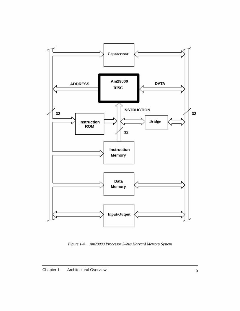
9Chapter 1 Architectural Overview
Coprocessor
Am29000
RISC
InstructionROM
INSTRUCTION
InstructionMemory
Input/Output
DATAADDRESS
32
32
32
DataMemory
Bridge
Figure 1-4. Am29000 Processor 3–bus Harvard Memory System

10 Evaluating and Programming the 29K RISC Family
All processors in the 29K family support byte and half–word size read and writeaccess to data memory. The original Am29000 (pre rev–D, 1990) only supportedword sized data access. This resulted in read–modify–write cycles to modify sub–word sized objects. The processor supports insert– and extract–byte and half–wordinstructions to assist with sub–word operations. These instructions are little usedtoday.
The processor has a Branch Target Cache (BTC) memory which is used to sup-ply the first four instructions of previously taken branches. Successful branches are20% of a typical instruction mix. Using burst–mode and interleaf techniques,memory systems can sustain the high bandwidths required to keep the instructionhungry RISC fed. However, when a branch occurs, memory systems can present con-siderable latency before supplying the first instruction of the branch target. For ex-ample, consider an instruction memory system which has a 3–cycle first access laten-cy but can sustain 1–cycle access in burst–mode. Typically every 5th instruction is abranch and for the example the branch instruction would take effectively 5–cycles tocomplete its execution (the pipeline would be stalled for 4–cycles (see section 1.13)).If all other instructions were executed in a single–cycle the average cycle time perinstruction would be 1.8 (i.e. 9/5); not the desired sustained single–cycle operation.The BTC can hide all 3–cycles of memory access latency, and enable the branchinstruction to execute in a single–cycle.
The programmer has little control over BTC operation; it is maintained internal-ly by processor hardware. There are 32 cache entries (known as cache blocks) of fourinstructions each. They are configured in a 2–way set associative arrangement. En-tries are tagged to distinguish between accesses made in User mode and Supervisormode; they are also tagged to differentiate between virtual addresses and physicaladdresses. Because the address in the program counter is presented to the BTC at thesame time it is presented to the MMU, the BTC does not operate with physical ad-dresses. Entries are not tagged with per–process identifiers; consequently the BTCcan not distinguish between identical virtual addresses belonging to different pro-cesses operating with virtual addressing. Systems which operate with multiple tasksusing virtual addressing must invalidate the cache when a user–task context switchoccurs. Using the IRETINV (interrupt return and invalidate) instruction is one con-venient way of doing this.
The BTC is able to hold the instructions of frequently taken trap handler rou-tines, but there is no means to lock code sequences into the cache. Entries are replacedin the cache on a random basis, the most recently occurring branches replacing thecurrent entries when necessary.
The 3–bus members of the the 29K family can operate the shared address bus ina pipeline mode. If a memory system is able to latch an address before an instructionor data transfer is complete, the address bus can be freed to start a subsequent access.

11Chapter 1 Architectural Overview
Allowing two accesses to be in progress simultaneously can be effectively used bythe separate instruction and data memory systems of a Harvard architecture.
1.3.1 The Am29005
The Am29005 is pin compatible with other 3–bus members of the family (seeTable 1-1). It is an inexpensive version of the Am29000 processor. The TranslationLook–Aside Buffer (TLB) and the Branch Target Cache (BTC) have been omitted. Itis available at a lower clock speed, and only in the less expensive plastic packaging. Itis a good choice for systems which are price sensitive and do not require MemoryManagement Unit support or the performance advantages of the BTC. An Am29005design can always be easily upgraded with an Am29000 replacement later. In fact thesuperior debugging environment offered by the Am29000 or the Am29050 maymake the use of one of these processor a good choice during software debugging. Thefaster processor can always be replaced by an Am29005 when production com-mences.
1.4 THE Am29050 3–BUS FLOATING–POINT MICROPROCESSOR
The Am29050 processor is pin compatible with other 3–bus members of thefamily (see Table 1-1) [AMD 1991a]. Many of the features of the Am29050 were al-ready described in the section describing its closely related relative, the Am29000.The Am29050 processor offers a number of additional performance and system sup-port features when compared with the Am29000. The most notable is the directexecution of double–precision (64–bit) and single–precision (32–bit) floating–pointarithmetic on–chip. The Am29000 has to rely on software emulation or theAm29027 floating–point coprocessor to perform floating–point operations. Theintroduction of the Am29050 eliminated the need to design the Am29027 coproces-sor into floating–point intensive systems.
The processor contains a Branch Target Cache (BTC) memory system like theAm29000; but this time it is twice as big, with 32 entries in each of the two sets ratherthan the Am29000’s 16 entries per set. BTC entries are not restricted to four instruc-tions per entry; there is an option (bit CO in the CFG register) to arrange the BTC as64 entries per set, with each entry containing two instructions rather than four. Thesmaller entry size is more useful with lower latency memory systems. For example, ifa memory system has a 2–cycle first–access start–up latency it is more efficient tohave a larger number of 2–instruction entries. After all, for this example system, thethird and fourth instructions in a four per entry arrangement could just as efficientlybe fetched from the external memory.
The Am29050 also incorporates an Instruction Forwarding path which addi-tionally helps to reduce the effects of instruction memory access latency. When a newinstruction fetch sequence commences, and the target of the sequence is not found in

12 Evaluating and Programming the 29K RISC Family
the BTC, an external memory access is performed to start filling the Instruction Pre-fetch Buffer (IPB). With the Am29000 processor the fetch stage of the processorpipeline is fed from the IPB, but the Am29050 can by–pass the fetch stage and feedthe first instruction directly into the decode pipeline stage using the instruction for-warding technique. By–passing also enables up to four cycles of external memorylatency to be hidden when a BTC hit occurs (see section 1.10).
The Am29050 incorporates a Translation Look–Aside Buffer (TLB) forMemory Management Unit support, just like the Am29000 processor. However italso has two region mapping registers. These permit large areas of memory to bemapped without using up the smaller TLB entries. They are very useful for mappinglarge data memory regions, and their use reduces the TLB software managementoverhead.
The processor can also speed up data memory accesses by making the accessaddress available a cycle earlier than the Am29000. The method is used to reducememory load operations which have a greater influence on pipeline stalling thanstore operations. Normally the address of a load appears on the address bus at the startof the cycle following the execution of the load instruction. If virtual addressing is inuse, then the TLB registers are used to perform address translation during the secondhalf of the load execute–cycle. To save a cycle, the Am29050 must make the physicaladdress of the load available at the start of the load instruction execution. It has twoways of doing this.
The access address of a load instruction is specified by the RB field of theinstruction (see Figure 1–13). A 4–entry Physical Address Cache (PAC) memory isused to store most recent load addresses. The cache entries are tagged with RB fieldregister numbers. When a load instruction enters the decode stage of the pipeline, theRB field is compared with one of the PAC entries, using a direct mapping technique,with the lower 2–bits of the register number being used to select the PAC entry. Whena match occurs the PAC supplies the address of the load, thus avoiding the delay ofreading the register file to obtain the address from the register selected by the RB fieldof the LOAD instruction. If a PAC miss occurs, the new physical address is written tothe appropriate PAC entry. The user has no means of controlling the PAC; its opera-tion is completely determined by the processor hardware.
The second method used by the Am29050 processor to reduce the effect of pipe-line stalling occurring as a result of memory load latency is the Early Address Gener-ator (EAG). Load addresses are frequently formed by preceding the load withCONST, CONSTH and ADD type instructions. These instructions prepare a generalpurpose register with the address about to be used during the load. The EAG circuitrycontinually generates addresses formed by the use of the above instructions in thehope that a load instruction will immediately follow and use the address newlyformed by the preceding instructions. The EAG must make use of the TLB addresstranslation hardware in order to make the physical address available at the start of the

13Chapter 1 Architectural Overview
load instruction. This happens when, fortunately, the RB field of the load instructionmatches with the destination register of the previous address computation instruc-tions.
Software debugging is better supported on the Am29050 processor than on anyother current 29K family member. All 29K processors have a trace facility which en-ables single stepping of processor instructions. However, prior to the Am29050 pro-cessor, tracing did not apply to the processor operation while the DA bit (disable alltraps and interrupts) was set in the current processor status (CPS) register. The DA bitis typically set while the processor is operating in Freeze mode (FZ bit set in the CPSregister). Freeze mode code is used during the entry and exit of interrupt and traphandlers, as well as other critical system support code. The introduction of Monitormode operation with the Am29050 enables tracing to be extended to Freeze modecode debugging. The processor enters Monitor mode when a synchronous trap oc-curs while the DA bit is set. The processor is equipped with a second set of PC bufferregisters, known as the shadow PC registers, which record the PC–bus activity whilethe processor is operating in Monitor mode. The first set of PC buffer registers havetheir values frozen when Freeze mode is entered.
The addition of two hardware breakpoint registers aids the Am29050 debugsupport. As instructions move into the execute stage of the processor pipeline, theinstruction address is compared with the break address values. The processor takes atrap when a match occurs. Software debug tools, such as monitors like Mini-MON29K, used with other 29K family members, typically use illegal instructions toimplement breakpoints. The use of breakpoint registers has a number of advantagesover this technique. Breakpoints can be placed in read–only memories, and break ad-dresses need not be physical but virtual, tagged with the per–process identifier.
1.5 THE Am29030 2–BUS MICROPROCESSOR
The Am29030 processor is pin compatible with other 2–bus members of thefamily (see Table 1-2) [AMD 1991b]. It was the first member of the 2–bus familyintroduced in 1991. Higher device construction densities enable it to offer high per-formance with a simplified system interface design. From a software point of viewthe main differences between it and the Am29000 processor occur as a result of re-placing the Branch Target Cache (BTC) memory with 8k bytes of instruction cache,and connecting the instruction and data busses together on–chip. However, the sys-tem interface busses have gained a number of important new capabilities.
The inclusion of an instruction cache memory reduces off–chip instructionmemory access bandwidth requirements. This enables instructions to be fetched viathe same device pins used by the data bus. Only when instructions can not be suppliedby the cache is there contention for access to external memory. Research [Hill 1987]has shown that with cache sizes above 4k bytes, a conventional instruction cache is

14 Evaluating and Programming the 29K RISC Family
Instruction Cache
Processor
I–Cache Associativity
On–Chip Floating–Point
On–Chip MMU
Narrow Memory Reads
On–Chip InterruptController Input’s
Am29030
8K bytes
2–Way
No
Yes
Yes, 8/16 bit
Yes6
Am29035
4K bytes
Direct–Mapped
No
Yes
Yes, 8/16 bit
JTAG Debugging Yes Yes
Yes6
Programmable Bus Sizing No Yes, 16/32 bit
Table 1-2. Pin Compatible 2–bus 29K Family Processors
Date Cache (Physical) – –
D–Cache Associativity – –
Integer Multiply in h/w No No
DMA Channels – –
Byte Endian Big/Little Big/Little
Scalable Clocking 1x,2x 1x,2x
Burst–mode Addressing Yes, up to 1K bytes Yes, up to 1K bytes
Freeze Mode Processing Yes Yes
Delayed Branching Yes Yes
On–Chip Timer Yes Yes
On–Chip Memory Controler No No
Clock Speeds (MHz) 20,25,33 16
Am29040
8K bytes
2–Way
No
Yes
Yes, 8/16 bit
Yes
Yes6
Yes, 16/32 bit
4K bytes
2–Way
Yes, 2–cycles
–
Big/Little
1x,2x
Yes, up to 1K bytes
Yes
Yes
Yes
No
0–33,40,50

15Chapter 1 Architectural Overview
more effective than a BTC. At these cache sizes the bandwith requirements are suffi-ciently reduced as to make a shared instruction/data bus practicable.
Each cache entry (known as a block) contains four consecutive instructions.They are tagged in a similar manner to the BTC mechanism of the Am29000 proces-sor. This allows cache entries to be used for both User mode and Supervisor modecode at the same time, and entries to remain valid during application system calls andsystem interrupt handlers. However, since entries are not tagged with per–processidentifiers, the cache entries must be invalidated when a task context switch occurs.The cache is 2–way set associative. The 4k bytes of instruction cache provided byeach set results in 256 entries per set (each entry being four instructions, i.e. 16 bytes).
When a branch instruction is executed and the block containing the targetinstruction sequence is not found in the cache, the processor fetches the missingblock and marks it valid. Complete blocks are always fetched, even if the targetinstruction lies at the end of the block. However, the cache forwards instructions tothe decoder without waiting for the block to be reloaded. If the cache is not disabledand the block to be replaced in the cache is not valid–and–locked, then the fetchedblock is placed in the cache. The 2–way cache associativity provides two possiblecache blocks for storing any selected memory block. When a cache miss occurs, andboth associated blocks are valid but not locked, a block is chosen at random for re-placement.
Locking valid blocks into the cache is not provided for on a per–block basis butin terms of the complete cache or one set of the two sets. When a set is locked, validblocks are not replaced; invalid blocks will be replaced and marked valid and locked.Cache locking can be used to preload the cache with instruction sequences critical toperformance. However, it is often difficult to use cache locking in a way that can out–perform the supported random replacement algorithm.
The processor supports Scalable Clocking which enables the processor to op-erate at the same or twice the speed of the off–chip memory system. A 33 MHz pro-cessor could be built around a 20 MHz memory system, and depending on cache uti-lization there may be little drop–off in performance compared to having constructeda 33 MHz memory system. This provides for higher system performance without in-creasing memory system costs or design complexity. Additionally, a performanceupgrade path is provided for systems which were originally built to operate at lowerspeeds. The processor need merely be replaced by a pin–compatible higher frequen-cy device (at higher cost) to realize improved system performance.
Memory system design is further simplified by enforcing a 2–cycle minimumaccess time for data and instruction accesses. Even if 1–cycle burst–mode is sup-ported by a memory system, the first access in the burst is hardwired by the processorto take 2–cycles. This is effective in relaxing memory system timing constraints andgenerally appreciated by memory system designers. The high frequency operation ofthe Am29030 processor can easily result in electrical noise [AMD1992c]. Enforcing

16 Evaluating and Programming the 29K RISC Family
2–cycle minimum access times ensures that the address bus has more time to settlebefore the data bus is driven. This reduces system noise compared with the data buschanging state during the same cycle as the address bus.
At high processor clock rates, it is likely that an interleafed memory system willbe required to obtain bandwidths able to sustain 1–cycle burst mode access. Inter-leafing requires the construction of two, four or more memory systems (known asbanks), which are used in sequence. When accessed in burst–mode, each bank is giv-en more time to provide access to its next storage location. The processor provides aninput pin, EARLYA (early address), by which a memory system can request early ad-dress generation by the processor. This can be used to simplify the implementation ofinterleaved memory systems. When requested, the processor provides early the ad-dress of even–addressed banks, allowing the memory system to begin early accessesto both even– and odd–addressed banks.
The processor can operate with memory devices which are not the full 32–bitwidth of the data bus. This is achieved using the Narrow Read capability. Memorysystems which are only 8–bit or 16–bit wide are connected to the upper bits of thedata/instruction bus. They assert the RDN (read narrow) input pin along with theRDY (ready) pin when responding to access requests. When this occurs the processorwill automatically perform the necessary sequences of accesses to assemble instruc-tions or data which are bigger than the memory system width.
The Narrow Read ability can not be used for data writing. However, it is veryuseful for interfacing to ROM which contains system boot–up code. Only a single8–bit ROM may be required to contain all the necessary system initialization code.This can greatly simplify system design, board space, and cost. The ROM can be usedto initialize system RAM memory which, due to its 32–bit width, will permit fasterexecution.
1.5.1 Am29030 Evaluation.
AMD provides a low cost evaluation board for the Am29030 at 16 MHz, knownas the EZ030 (pronounced easy–030). Like the microcontroller evaluation board, it isa standalone, requiring an external 5v power supply and connection to a remote com-puter via an RS–232 connection. The board is very small, measuring about 4 inchesby 4 inches (10x10 cm). The memory system is restricted to 16 MHz operation butwith scalable clocking the processor can run at 16 MHz or 33 MHz.
It contains 128k bytes of EPROM, which is accessed via 8–bit narrow bus proto-col. There is also 1M byte of DRAM arranged as 256kx32 bits. The DRAM is ex-pandable to 4M bytes. The EPROM is preprogrammed with the MiniMON29K de-bug monitor and the OS–boot operating system described in Chapter 7.
1.5.2 The Am29035
The Am29035 processor is pin compatible with other 2–bus members of thefamily (see Table 1-2). As would be expected, given the AMD product number, its

17Chapter 1 Architectural Overview
operation is very similar to the Am29030 processor. It is only available at lower clockfrequencies, compared with its close relative. And with half the amount of instructioncache memory, it contains one set of the two sets provided by the Am29030. That is, ithas 4k bytes of instruction memory cache which is directly mapped. Consequently itcan be expected to operate with reduced overall performance.
In all other aspects it is the same as the Am29030 processor, except it has Pro-grammable Bus Sizing which the Am29030 processor does not. Programmable BusSizing provides for lower cost system designs. The processor can be dynamicallyprogrammed (via the configuration register) to operate with a 16–bit instruction/databus, performing both read and write operations. When the option is selected, 32–bitdata is accessed by the processor hardware automatically performing two consecu-tive accesses. The ability to operate with 16–bit and 32–bit memory systems makesthe 2–bus 29K family members well suited to scalable system designs, in terms ofcost and performance.
1.6 THE Am29040 2–BUS MICROPROCESSOR
The Am29040 processor is pin compatible with other 2–bus members of thefamily (see Table 1-2). The processor was introduced in 1994 and offers higher per-formance than the 2–bus Am29030; it also has a number of additional system supportfacilities.
There is an enhanced instruction cache, now 8k bytes; which is tagged in muchthe same way as the Am29030’s instruction cache, except there are four valid bits percache block (compared to the Am29030’s one bit per block). Partially filled blocksare supported, and block reload begins with the first required instruction (target of abranch) rather than the first instruction in the block. An additional benefit of having avalid bit per–instruction rather than per–block is that load or store instructions caninterrupt cache reload. With the Am29030 processor, once cache reload had started,it could not be postponed or interrupted by a higher priority LOAD instruction.
The Am29040 was the first 29K microprocessor to have a data cache. The 4kbyte data cache is physically addressed and supports both “copy–back” and “write–through” policies. Like other 29K Family members, the data cache always operateswith physical addresses and cache blocks are only allocated on LOAD instructionswhich miss (a “read–allocate” or “load–allocate” policy). The block size is 16 bytesand there is one valid bit per block. This means that complete data blocks must befetched when data cache reload occurs. Burst mode addressing is used to reload ablock, starting with the first word in the block. The addition of a data cache makes theAm29040 particularly well–suited to high–performance data handling applications.
The default data cache policy is “copy–back”. A four word copy–back buffer isused to improve the performance of the copy–back operation. Additionally, cacheblocks have an M bit–field, which becomes set when data in the block is modified. If

18 Evaluating and Programming the 29K RISC Family
the M bit is not set when a cache block is reallocated, the out–going block is not co-pied back.
When data cache is added to a processor, there can be difficulties dealing withdata consistency. Problems arise when there is more than one processor or data con-troller (such as a DMA controller) accessing the same memory region. The Am29040processor uses bus snooping to solve this problem. The method relies on the proces-sor monitoring all accesses performed on the memory system. The processor inter-venes or updates its cache when an access is attempted on a currently cached datavalue. Cache consistency is dealt with in detail in section 5.14.4.
Via the MMU, each memory page can be separately marked as “non cached”,“copy–back”, or “write–through”. A two word write–through buffer is used to assistwith writes to memory. It enables multiple store instructions to be in–execution with-out the processor pipeline stalling. Data accesses which hit in the cache require2–cycle access times. Two cycles, rather than one, are required due to the potentiallyhigh internal clock speed. The data cache operation is explained in detail in section5.14.2. However, load instructions do not cause pipeline stalling if the instruction im-mediately following the load does not require the data being accessed.
Scalable bus clocking is supported; enabling the processor to run at twice thespeed of the off–chip memory system. Scalable Clocking was first introduced withthe Am29030 processors, and is described in the previous section describing theAm29030. If cache hit rates are sufficiently high, Scalable Clocking enables highperformance systems to be built around relatively slow memory systems. It also of-fers an excellent upgrade path when additional performance is required in the future.The maximum on–chip clock speed is 50 MHz.
The Am29040 processor supports integer multiply directly. A latency of twocycles applies to integer multiply instructions (most 29K instructions require onlyone cycle). Again, this is a result of the potentially high internal clocking speeds ofthe processor. Most 29K processors take a trap when an integer multiply is attempted.It is left to trapware to emulate the missing instruction. The ability to perform highspeed multiply makes the processor a better choice for calculation intensive applica-tions such as digital signal processing. Note, floating–point performance should alsoimprove with the Am29040 as floating–point emulation routines can make use of theinteger multiply instruction.
The Am29040 has two Translation Look–Aside Buffers (TLBs). Having twoTLBs enables a larger number of virtual to physical address translations to be cached(held in a TLB register) at any time. This reduces the TLB reload overhead. The TLBformat is similar to the arrangement used with the Am29243 microcontroller. EachTLB has 16 entries (8 sets, two entries per set). The page size used by each TLB canbe the same or different. If the TLB page sizes are the same, a four–way set associa-tive MMU can be constructed with supporting software. Alternatively one TLB canbe used for code and the second, with a larger page size, for data buffers or shared
19Chapter 1 Architectural Overview
libraries. The TLB entries have a Global Page (GLB) bit; when set the mapped pagecan be accessed by any processes regardless of its process identifier (PID). The TLBalso enables parity checking to be enabled on a per page basis; and pages can be allo-cated from 16–bit or 32–bit wide memory regions.
On–chip debug support is extended with the inclusion of two Instruction Break-point Controllers and one Data Breakpoint Controller. This enables inexpensive de-bug monitors such as the DebugCore incorporated within MiniMON29K to be usedwhen developing software. Breakpoints are supported when physical or virtual ad-dressing is in use. The JTAG test interface has also been extended over other 29Kfamily members to include several new JTAG–processed instructions. The effective-ness of the JTAG interface for hardware and software debugging is improved.
The Am29040 family grouping is implemented with a silicon process which en-ables processors to operate at 3.3–volts. However, the device is tolerant of 5–volt in-put/output signal levels. The lower power consumption achievable at 3.3–voltsmakes the Am29040 suitable for hand–held type applications. Note, the device oper-ates at a maximum clock frequency of 50 MHz.
A 29K processor enters Wait Mode when the Wait Mode bit is set in the CurrentProcessor Status (CPS) register. Wait Mode is extended to include a Snooze Modewhich is entered from Wait Mode while the interrupt and trap input lines are held in-active. An interrupt is normally used to depart Wait or Snooze Mode. While inSnooze mode, Am29040 power consumption is reduced. Returning from Snoozemode to an interrupt processing state requires approximately 256 cycles. The proces-sor can be prevented from entering Snooze Mode while in Wait Mode by holding, forexample, the INTR3 input pin active and setting the interrupt mask such as to disablethe INTR3 interrupt.
If the input clock is held high or low while the processor is in Snooze mode,Sleep Mode is entered. Minimum power consumption occurs in this mode. The pro-cessor returns to Snooze Mode when the input clock is restarted. Using Snooze andSleep modes enables the Am29040 processor to be used in applications which arevery power sensitive.
1.6.1 Am29040 Evaluation.
Like any 29K processor, the Am29040 can be evaluated using the ArchitecturalSimulator. But for those who wish for real hardware, AMD manufactures a numberof evaluation boards. The most popular being the SE29040 evaluation board. Theboard, originally constructed in rev–A form, supports 4M bytes of DRAM (expand-able to 64M bytes); DRAM timing is 3/1, i.e. 3–cycle first access then 1–cycle burst.There is also 1M byte of 32–bit wide ROM and space for 1M byte of 2/1 SRAM.Boards are typically populated with only 128K of SRAM. The memory system clockspeed is 25 MHZ and the maximum processor speed of 50 MHz is supported.
20 Evaluating and Programming the 29K RISC Family
There are connections for JTAG and a logic analyzer as well as two UARTs viaan 85C30 serial communications controller. The board requires a 5–volt power sup-ply and there is a small wire–warp area for placement of additional system compo-nents.
The later rev–B boards have an additional parallel port and Ethernet connection(10–base–T). An AMD HiLANCE is used for Ethernet communication. The rev–Bboard can also support memory system speeds up to 33 MHz.
1.7 A SUPERSCALAR 29K PROCESSOR
AMD representatives have talked at conferences and to the engineering pressabout a superscalar 29K processor. No announcements have yet been made aboutwhen such a processor will be available, but it is generally expected to be in the nearfuture. At the 1994 Microprocessor Forum, AMD presented a product overview, butmuch of the specific details about the processor architecture were not announced.However, piecing together available information, it is possible to form ideas aboutwhat a superscalar 29K would look like.
This section does not describe a specific processor, but presents the superscalartechniques which are likely to be utilized. A lead architect of the 29K family, MikeJohnson, has a text book dealing with “Superscalar Microprocessor Design” ([John-son 1991]) which covers the technology in depth. It might be expected that many ofthe conclusions drawn in Johnson’s book will appear in silicon in a future 29K pro-cessor.
AMD has stated that future microprocessors will be pin compatible with the cur-rent 2–bus family members. This indicates that a superscalar 29K will be pin compat-ible with the Am29030 and Am29040 processors. It is much more likely that the pro-cessor will take 2–bus form rather than a microcontroller. User mode instructioncompatibility can also be expected. Given the usual performance increments that ac-company a new processors introduction, it will likely sustain two–times the perfor-mance of an Am29040 processor. This may be an underestimate, as higher clock ratesor increased use of Scalable Clocking may allow for even higher performance. Theprocessor is certain to have considerable on–chip instruction and data cache. AMD’sproduct overview indicates that 2x, 3x and 4x Scalable Clocking will be supportedand there will be an 8K byte instruction cache and an 8K byte data cache. Also re-ported was an internal clock speed up to 100 MHz at 3.3–volts.
A superscalar processor achieves higher performance than a conventional sca-lar processor by executing more than one instruction per cycle. To achieve this it musthave multiple function units which can operate in parallel. AMD has indicated thatthe initial superscalar 29K processor will have six function units. And since about50% of instructions perform integer operations, there will be two integer operationunits, one integer multiplier and one funnel shifter. If a future the processor supportsfloating–point operations directly, we can expect to see a floating–point execution
21Chapter 1 Architectural Overview
unit added. Other execution units are included to deal with off–chip access via loadand store instructions; and to deal with branch instruction execution. All six functionunits, except the integer multiplier, produce their results in a single–cycle.
High speed operation can only be obtained if as many as possible of the functionunits can be kept productively busy during the same processor cycles. This will placea heavy demand on instruction decoding and operand forwarding. Several instruc-tions will have to be decoded in the same cycle and forwarded to the appropriateexecution unit. The demand for operands for these instructions shall be considerablyhigher than must be dealt with by a scalar processor. The following sections describesome of the difficulties encountered when attempting to execute more than oneinstruction per cycle. Architectural techniques which overcome the inherent difficul-ties are presented.
1.7.1 Instruction Issue and Data Dependency
The term instructions issue refers to the passing of an instruction from the pro-cessor decode stage to an execution unit. With a scalar processor, instructions are is-sued in–order. By that, I mean, in the order the decoder received the instructions fromcache or off–chip memory. Instructions naturally complete in–order. However with aRISC processor out–of–order completion is not unusual for certain instructions. Typ-ically load and store instructions are allowed to execute in parallel with other instruc-tions. These instructions are issued in–order; they don’t complete immediately butsome time (a few cycles) later. The instructions following loads or stores are issuedand execute in parallel unless there is any data dependencies. Dependencies arisewhen, for example, a load instructions is followed by an operation on the loaded data.
A superscalar processor can reduce total execution time for a code sequence if itallows all instruction types to complete out–of–order. Instruction issue need not stopafter an instruction is issued to a function unit which takes multiple cycles to com-plete. Consequently, function units with long latency may complete their operationafter a subsequent instruction issued to a low latency function unit. The Am29050processor allows long latency floating–point operations to execute in parallel withother integer operations. The processor has an additional port on it’s register file forwriting–back the results of floating–point operations. An additional port is requiredto avoid the contention which would arise with an integer operation writing back itsresult at the same time. Most instructions are issued to an integer unit which, with aRISC processor, has only one cycle latency. However, there is very likely to be morethan one integer unit, each operating in parallel.

22 Evaluating and Programming the 29K RISC Family
Write–Read Dependency
Even if a processor is able to support out–of–order instruction completion, itstill must deal with the data dependencies that flow through a program’s execution.These flow dependencies (often known as true dependencies) represent the move-ment of operands between instructions in a program.Examine the code below:
mul gr96,lr2,lr5 ;write gr96, gr96 = lr2 * lr5add gr97,gr96,1 ;read gr96, write–read dependency
The first instruction would be issued to the integermultiply unit; this will have (according to AMD’sproduct overview) two cycles of latency. The result iswritten to register gr96. The second instruction wouldbe issued to a different integer handling unit. However,it has a source operand supplied in gr96. If the secondinstruction had no data dependencies on the first, itwould be easy to issue the instruction while the first wasstill in execute. However, execution of the firstinstruction must complete before the second instructioncan start execution. Steps must be taken to deal with thedata dependency. This kind of dependency is also knowas write–read dependency, because gr96 must bewritten by an earlier instruction before a later one canread the result.
Some superscalar processors, such as the Intel i960 CA, use areduced–scoreboarding mechanism to resolve data dependances [Thorton 1970].When a register is required for a result, a one–bit flag is set to indicate the register is inuse. Currently in–execute instructions set the scoreboard bit for their result registers.Before an instruction is issued the scoreboard bit is examined. Further instructionsare not issued if the scoreboard indicates that an in–execute instruction intends towrite a register which supplies a source operand for the instruction waiting for issue.When an instruction completes, the relevant scoreboard bit is cleared. This mayresult in a currently stalled instruction being issued.
It is unlikely a 29K processor will use scoreboarding; and even less likely it willuse a reduced–scoreboarding mechanism, such as the i960 CA, which only detectsdata dependency for out–of–order instruction completion. A superscalar 29Kprocessor will support out–of–order instruction issue, which is described shortly.Scoreboarding can resolve the resulting data dependencies. However, othertechniques, such as register renaming, enable instructions to be decoded and issuedfurther ahead than is possible with scoreboarding. This will be described in moredetail as we proceed.
mul
add
gr96
lr5lr2
gr97
1
23Chapter 1 Architectural Overview
Write–Write Dependency
A second type of data dependency can complicate out–of–order instructioncompletion. Examine the code sequence shown below:
mul gr96,lr2,lr5 ;write gr96, gr96 = lr2 * lr5add gr97,gr96,1add gr96,lr5,1 ;write gr96, write–write dependency
The result of the third instruction has an output dependency on the firstinstruction. The third instruction can not complete before the first. Both instructionswrite their results to register gr96, and completing the first instruction last wouldresult in an out–of–date value being held in gr96. Steps must be taken to deal with thedata dependency. Because the completion of multiple instructions is dependent onwriting gr96 with the correct value, this kind of dependence is also known as awrite–write dependance.
Scoreboarding or reduced–scoreboarding can also resolve write–writedependences. Before an instruction is issued, the scoreboard bit for the result registeris tested. If there is a currently in–execute instruction planning on writing to the sameresult register, the scoreboard bit will be set. This information can be used to stallissuing until the result register is available.
The parallel execution possible with out–of–order completion, enables higherperformance than in–order completion, but extra logic is required to deal with datadependency checking. With in–order instruction issue, instructions can no longer beissued when a dependency is detected. If instruction issue is to continue when datadependencies are present, the processor architecture becomes yet more complicated;but the performance reward is extended beyond that of out–of–order completionwith in–order issue.
Read–Write Dependency
Instruction issuing can continue even when the write–read and write–writedependencies described above are present. The preceding discussion on datadependency was restricted to in–order instruction issue. Certainly, when a datadependency is detected, the unfortunate instruction can not be issued; but this neednot mean that future instructions can not be issued. Of course the future instructionmust be free of any dependencies. With out–of–order instruction issue, instructionsare decoded and placed in an instruction window. Instructions can be issued from thewindow when they are free of dependencies and there is an available function unit.
The processes of decoding and executing an instruction is separated by theinstruction window, see Figure 1-5. This does not add an additional pipeline stage tothe superscalar processor. The decoder places instructions into the window. When aninstruction is free of dependencies it can be issued from the window to a function unitfor execution. The register window could be implemented as a large buffer within theinstruction decode unit, but this leads to a complex architecture. When an instruction
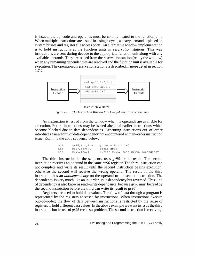
24 Evaluating and Programming the 29K RISC Family
is issued, the op–code and operands must be communicated to the function unit.When multiple instructions are issued in a single cycle, a heavy demand is placed onsystem busses and register file access ports. An alternative window implementationis to hold instructions at the function units in reservation stations. This wayinstructions are sent during decode to the appropriate function unit along with anyavailable operands. They are issued from the reservation station (really the window)when any remaining dependencies are resolved and the function unit is available forexecution. The operation of reservation stations is described in more detail in section1.7.2.
Figure 1-5. The Instruction Window for Out–of–Order Instruction Issue
InstructionDecode
Instruction Window
InstructionExecute
mul gr96,lr2,lr5
add gr97,gr96,1
add gr96,lr5,1
An instruction is issued from the window when its operands are available forexecution. Future instructions may be issued ahead of earlier instructions whichbecome blocked due to data dependencies. Executing instructions out–of–orderintroduces a new form of data dependency not encountered with in–order instructionissue. Examine the code sequence below:
mul gr96,lr2,lr5 ;gr96 = lr2 * lr5add gr97,gr96,1 ;read gr96add gr96,lr5,1 ;write gr96, read–write dependency
The third instruction in the sequence uses gr96 for its result. The secondinstruction receives an operand in the same gr96 register. The third instruction cannot complete and write its result until the second instruction begins execution;otherwise the second will receive the wrong operand. The result of the thirdinstruction has an antidependency on the operand to the second instruction. Thedependency is very much like an in–order issue dependency but reversed. This kindof dependency is also know as read–write dependance, because gr96 must be read bythe second instruction before the third can write its result to gr96.
Registers are used to hold data values. The flow of data through a program isrepresented by the registers accessed by instructions. When instructions executeout–of–order; the flow of data between instructions is restricted by the reuse ofregisters to hold different data values. In the above example we want to issue the thirdinstruction but its use of gr96 creates a problem. The second instruction is receiving,

25Chapter 1 Architectural Overview
via gr96, a data value produced by the first instruction. The register label gr96 ismerely used as an identifier for the data flow. What is intended is that data be passedfrom the first instruction to the second. If our intentions could be communicatedwithout restricting data passing to gr96, then the third instruction could be executedbefore the second.
The problem can be overcome by using register renaming, see section 1.7.3.Briefly, when the first instruction in the above example is issued, it writes its result toa temporary register identified by the name gr96. The second instruction receives itsoperand from the same temporary register used by the first instruction. Execution ofthe third instruction need not be stalled if it writes its result to a different copy ofregister gr96. So now there are multiple copies of gr96. What really happens istemporary registers are renamed to be gr96 for the duration of the data flow. Thesetemporary registers play the role of registers indicated by the instruction sequence.They are tagged to indicate the register they are duplicating.
1.7.2 Reservation Stations
Each function unit has a number of reservation stations which hold instructionsand operands waiting for execution, see Figure 1-6. All the reservation stations foreach function unit combined represent the instruction window from whichinstructions are issued. The decoder places instructions into reservation stations[Tomasulo 1967] with copies of operands, when available. Otherwise operand valuesare replaced with tags indicating the register supplying the missing data. Placing acopy of a source operand into the reservation station when an instruction is decoded,prevents the operand being updated by a future instruction; and hence eliminatesanidependency conflicts. A function unit issues instructions to its execute stage whenit is not busy and a reservation station has an instruction ready for execution. Once aninstruction is placed in a reservation station, its issue occurs regardless of anyinstruction issue occurring in another function unit. There can be any number ofreservation stations attached to a function unit. The greater the number, the larger theinstruction window; and the further ahead the processor can decode and issueinstructions. Additionally, a greater number of reservation stations prevents shortterm demands on a function unit resulting in decoder–stalling.
An instruction may be stalled in a reservation station when a data dependencycauses a tag, rather than data, to be placed in the operand field. The necessary datawill become available when some other instruction completes and the result madeavailable. The instruction producing the required data value may be in a reservationstation or in execution in the same function unit, or in another function unit. Resultvalues are tagged indicating the register they should be placed in. With a scalarprocessor, the result is always written to the instruction’s destination register. Butwhen register renaming is used by a superscalar processor, results are written to aregister which is temporarily playing the role of the destination register. These
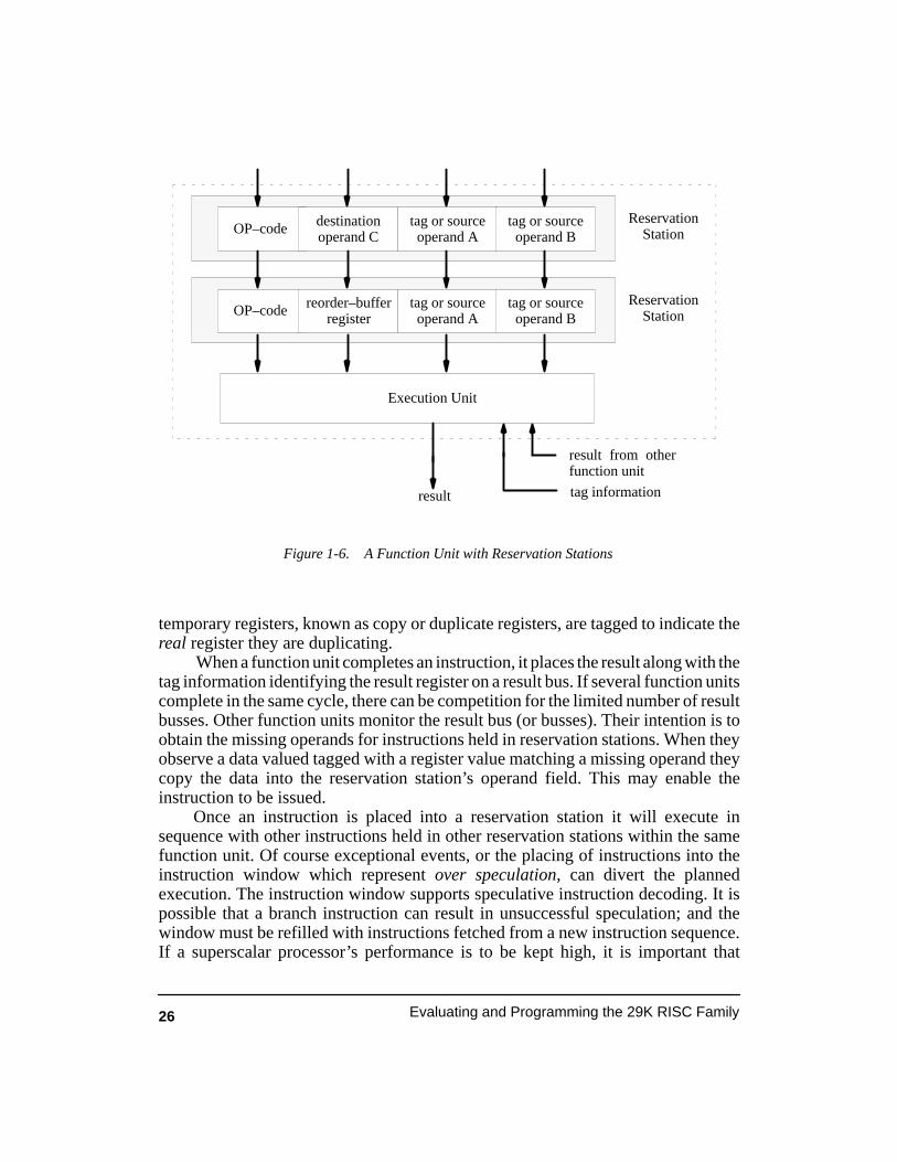
26 Evaluating and Programming the 29K RISC Family
Figure 1-6. A Function Unit with Reservation Stations
result
ReservationStation
Execution Unit
result from otherfunction unit
tag information
OP–code destinationoperand C
tag or sourceoperand A
tag or sourceoperand B
ReservationStationOP–code reorder–buffer
registertag or sourceoperand A
tag or sourceoperand B
temporary registers, known as copy or duplicate registers, are tagged to indicate thereal register they are duplicating.
When a function unit completes an instruction, it places the result along with thetag information identifying the result register on a result bus. If several function unitscomplete in the same cycle, there can be competition for the limited number of resultbusses. Other function units monitor the result bus (or busses). Their intention is toobtain the missing operands for instructions held in reservation stations. When theyobserve a data valued tagged with a register value matching a missing operand theycopy the data into the reservation station’s operand field. This may enable theinstruction to be issued.
Once an instruction is placed into a reservation station it will execute insequence with other instructions held in other reservation stations within the samefunction unit. Of course exceptional events, or the placing of instructions into theinstruction window which represent over speculation, can divert the plannedexecution. The instruction window supports speculative instruction decoding. It ispossible that a branch instruction can result in unsuccessful speculation; and thewindow must be refilled with instructions fetched from a new instruction sequence.If a superscalar processor’s performance is to be kept high, it is important that

27Chapter 1 Architectural Overview
speculation be successful. For this to be accomplished, branch prediction techniquesmust be employed; more on this is in section 1.7.4.
1.7.3 Register Renaming
It was briefly described in the previous section dealing with read–writedependency (antidependency), that register renaming can help deal with the conflictswhich arise from the reuse of the same register to hold data values. Of course thesedependencies only arise from the out–of–order instruction issue which occurs with asuperscalar processor. Also described were write–write (output) dependencies,which occur with even in–order instruction issue when more than one instructionwishes to write the same result register. Both these types of dependency can begrouped under the heading storage conflicts. Their interference with concurrentinstruction execution is only temporary. Duplication of the result register for theduration of the conflict can resolve the dependency and enable superscalarinstruction execution to continue.
The temporary result registers are allocated from a reorder buffer whichconsists of 10 registers and supporting tag information. Every new result value isallocated a new copy of the original assignment register. Copies are tagged to enablethem to be used as source operands in future instructions. Register renaming is shownfor the example code sequence below.
;original code ;code after register renamingmul gr96,lr2,lr5 mul RR1,lr2,lr5 ;gr96 = lr2 * lr5add gr97,gr96,1 add RR2,RR1,1add gr96,lr5,1 add RR3,lr5,1
The write–write dependency between the first and third instruction is resolvedby renaming register gr96 to be register RR3 in the third instruction. The renaminggr96 to be RR3 in the third instruction also resolves the read–write dependencybetween the second and third instruction Using register renaming, execution of thethird instruction need not be stalled due to storage (register) dependency. Figure 1-7shows the dependencies before and after register renaming.
Let’s look in more detail at the operation of the reorder buffer. When an instruc-tion is decoded and placed in the instruction window (in practice, a reservation sta-tion), a register in the reorder buffer is assigned to hold the instruction result.Figure 1-8 shows the format of information held in the reorder buffer. When theinstruction is issued from the reservation station and, at a later time, execution com-pleted, the result is written to the assigned reorder buffer entry.
If a future instruction refers to the result of a previous instruction, the reorderbuffer is accessed to obtain the necessary value. The reorder buffer is accessed via thecontents of the destination–tag field. This is known as a content–addressablememory access. A parallel search of the reorder buffer is performed. All memorylocations are simultaneously examined to determine if they have the requested data.
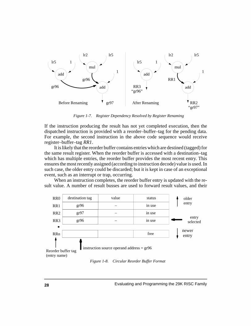
28 Evaluating and Programming the 29K RISC Family
mul
add
RR1
lr5lr2
RR2“gr97”
1add
RR3“gr96”
1lr5mul
add
gr96
lr5lr2
gr97
1add
gr96
1lr5
Figure 1-7. Register Dependency Resolved by Register Renaming
Before Renaming After Renaming
If the instruction producing the result has not yet completed execution, then thedispatched instruction is provided with a reorder–buffer–tag for the pending data.For example, the second instruction in the above code sequence would receiveregister–buffer–tag RR1.
It is likely that the reorder buffer contains entries which are destined (tagged) forthe same result register. When the reorder buffer is accessed with a destination–tagwhich has multiple entries, the reorder buffer provides the most recent entry. Thisensures the most recently assigned (according to instruction decode) value is used. Insuch case, the older entry could be discarded; but it is kept in case of an exceptionalevent, such as an interrupt or trap, occurring.
When an instruction completes, the reorder buffer entry is updated with the re-sult value. A number of result busses are used to forward result values, and their
Figure 1-8. Circular Reorder Buffer Format
destination tagRR0 value status
gr96RR1 – in use
gr97RR2 – in use
gr96RR3 – in use
RRn
instruction source operand address = gr96
entryselected
olderentry
newerentryfree
Reorder buffer tag(entry name)

29Chapter 1 Architectural Overview
associated tag information, to the reorder buffer. Function units monitor the flow ofdata along these buses in the hope of acquiring data values required by their reserva-tion stations. In this way, instructions are supplied the operands which where missingwhen the instruction was decoded. When a reorder buffer has been updated with aresult, the entry is ready for retiring. This is the term given to writing the result valueinto the real register in the register file. There is a bus for this task which connectsread ports on the reorder buffer to write ports on the register file. The number of portsassigned to this task (2) limits the number of instructions which can be retired in anyone processor cycle. A register file with two write ports supports a maximum of fourinstructions being retired during the same cycle; two instructions which modify re-sult registers, one store instruction, and one branch instruction (these last two instruc-tion types do not write to result registers). Figure 1-9 outlines the system layout.
When the reorder buffer becomes full, no further instruction decoding can occuruntil entries are made available via instruction retiring. Instructions are retired in theorder they are placed in the reorder buffer. This ensures in–order retiring ofinstructions. Should an exceptional event occur during program execution, the stateof instruction retirement specifies the precise position which execution has reachedwithin the program. Only completed instructions, without exceptions, are retired.
Figure 1-9. Multiple Function Units with a Reorder Buffer
Result and Tag Buses
FunctionUnit
FunctionUnit
FunctionUnit
ReorderBuffer
RegisterFileInstruction
Decode
Operand Buses
Instruction Bus
InstructionCache
InstructionMemory
reservationstations (2)
Retirement Bus
10 word
3 word
4 word
2 word
4 instructions
4 word

30 Evaluating and Programming the 29K RISC Family
Figure 1-9 shows the operand busses supplying source operands from thereorder buffer to the reservation stations. However, in some cases, when aninstruction is decoded and the operand register’s number presented to the reorderbuffer, no entry is found. This indicates there is currently no copy of the requiredregister. Consequently, the real register in the register file must be accessed to obtainthe data. For this reason the register file is provided with read ports (4) which supplydata to the operand bus.
1.7.4 Branch Prediction
Out–of–order instruction issue places a heavy demand on instruction decoding.If reservation stations are to be kept filled, instruction decode must proceed at a rateequal to, or greater than, instruction execution. Otherwise, performance will belimited by the ability to decode instructions. The major obstacle in the way ofachieving efficient decoder operation is branching instructions. Unfortunately,instruction sequences typically contain only about five or six instructions before afurther branch–type instruction is encountered. Compilers directed to producingcode specifically for superscalar processor execution try to increase this criticalparameter. Additionally, the fact that a target of a branch instruction need not bealigned on a cache block boundary, can further reduce the efficiency of the decodingprocesses.
The decoder fetches instructions and places them into the instruction windowfor issue by a function unit. If an average decode rate of more than two instructionsper cycle is to be achieved, it is likely that a four–instruction decoder (or better) willbe required. In fact, AMD’s product overview indicates a four–instruction decoder isused. To study this further, first examine the code below. The first target sequencebegins at address label L13. The linker need not align the L13 label at a cache blockboundary –– a cache block size of four instructions will be assumed. The samealignment issue occurs with the second target sequence beginning at label L14. Thedecoder is presented with a complete cache block rather than sequential instructionsfrom within the block. This requires a 128–bit bus between the instruction cache andthe decode unit. However, this is essential if instructions are to be decoded in parallel.Figure 1-10 shows a possible cache block assignment, assuming the target of the firstinstruction sequence begins in the second entry of the cache block. The target of thesecond sequence begins in the third instruction of the block.
L13: ;target of a branchadd gr98,gr98,10 ;gr98 = gr98 + 10sll gr99,gr99,2cpgt gr97,gr97,gr98jmpt gr97,L14 ;conditional branch to L14 add lr4,lr4,gr99 ;branch delay slot, see section 1.13
L15:load 0,0,gr97,lr4store 0,0,gr97,gr96
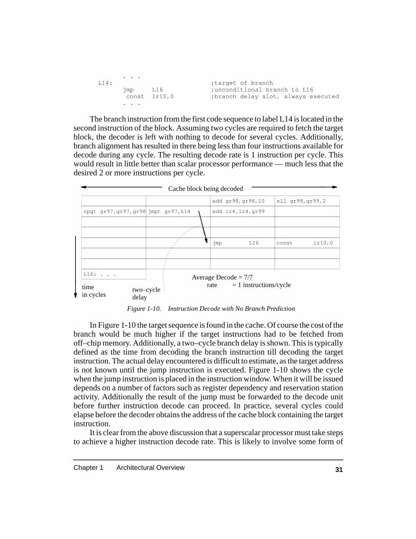
31Chapter 1 Architectural Overview
. . .L14: ;target of branch
jmp L16 ;unconditional branch to L16 const lr10,0 ;branch delay slot, always executed. . .
The branch instruction from the first code sequence to label L14 is located in thesecond instruction of the block. Assuming two cycles are required to fetch the targetblock, the decoder is left with nothing to decode for several cycles. Additionally,branch alignment has resulted in there being less than four instructions available fordecode during any cycle. The resulting decode rate is 1 instruction per cycle. Thiswould result in little better than scalar processor performance –– much less that thedesired 2 or more instructions per cycle.
Figure 1-10. Instruction Decode with No Branch Prediction
add gr98,gr98,10 sll gr99,gr99,2
cpgt gr97,gr97,gr98 jmpt gr97,L14 add lr4,lr4,gr99
jmp L16 const lr10,0
timein cycles
Average Decode = 7/7 rate = 1 instructions/cycle
L16: . . .
two–cycledelay
Cache block being decoded
In Figure 1-10 the target sequence is found in the cache. Of course the cost of thebranch would be much higher if the target instructions had to be fetched fromoff–chip memory. Additionally, a two–cycle branch delay is shown. This is typicallydefined as the time from decoding the branch instruction till decoding the targetinstruction. The actual delay encountered is difficult to estimate, as the target addressis not known until the jump instruction is executed. Figure 1-10 shows the cyclewhen the jump instruction is placed in the instruction window. When it will be issueddepends on a number of factors such as register dependency and reservation stationactivity. Additionally the result of the jump must be forwarded to the decode unitbefore further instruction decode can proceed. In practice, several cycles couldelapse before the decoder obtains the address of the cache block containing the targetinstruction.
It is clear from the above discussion that a superscalar processor must take stepsto achieve a higher instruction decode rate. This is likely to involve some form of

32 Evaluating and Programming the 29K RISC Family
branch prediction. The decoder can not wait for the outcome of the branch instructionto be know before it starts fetching the new instruction stream. It must examine theinstruction currently being decoded, and determine if a branch is present. When abranching instruction is found, the decoder must predict both if the branch will betaken and the target of the branch. This enables instructions to be fetched anddecoded along the predicted path. Of course, unconditional branches also benefitfrom early fetching of their target instruction sequence; and they do not requirebranch prediction support.
The instruction decode sequence for the previous code example is shown inFigure 1-11 using branch prediction. Without waiting for the conditional–jumpinstruction in the second entry of the cache block to execute, the decoder predicts thebranch will be taken and in the next cycle starts decoding the block containing thetarget instruction. This results in a decode rate of 2.33 instructions per cycle. If theprediction is correct, the decoder should be able to sustain a decode rate whichprevents starving the function units of instructions.
Figure 1-11. Four–Instruction Decoder with Branch Prediction
add gr98,gr98,10 sll gr99,gr99,2
cpgt gr97,gr97,gr98 jmpt gr97,L14 add lr4,lr4,gr99
jmp L16 const lr10,0
timein cycles
Average Decode = 7/3 rate = 2.33 instructions/cycle
Cache block being decoded
Branch prediction supports speculative instruction fetching. It results ininstructions being placed in the instruction window which may be speculativelydispatched and executed. If the branch is wrongly predicted, instructions still waitingin reservation stations must be cancelled. Any wrongly predicated instructions whichreach execution must not be retired. This requires considerable support circuitry. Forthis reason scoreboarding is used by some processors to support speculativeinstruction fetching. With scoreboarding the decoder sets a scoreboard bit for eachinstruction’s destination register. Since there is only one bit indicating there is apending update, there can be only one such update per register. Consequently, thedecoder stalls when encountering an instruction required to update a register whichalready has a pending update. The scoreboarding mechanism is simpler to implementthan register renaming using a reorder buffer. However, its restrictions limit thedecoder’s ability to speculatively fetch instruction further ahead of actual execution.This has been shown to result in about 21% poorer performance when afour–instruction decoder is used [Johnson 1991].

33Chapter 1 Architectural Overview
It is certain that a superscalar 29K processor will incorporate a branchprediction technique. Given that instruction compatibility is to be maintained, it islikely that a hardware prediction rather than a software prediction method will beemployed. This will require the processor to keep track of previous branch activity.An algorithm will likely help with selecting the most frequent branch paths; such asbranches to lower addresses are more often taken then not –– jump at bottom of loop.
1.8 THE Am29200 MICROCONTROLLER
The Am29200 was the first of the 29K family microcontrollers (seeTable 1-3) [AMD 1992b]. To date the Am29205 is the only other microcontrolleradded to the family. Being microcontrollers, many of the device pins are assigned I/Oand other dedicated support tasks which reduce system glue logic requirements. Forthis reason none of the devices are pin compatible. The system support facilities, in-cluded within the Am29200 package, make it ideal for many highly integrated andlow cost systems.
The processor supports a 32–bit address space which is divided into a number ofdedicated regions (see Figure 1-12). This means that ROM, for example, can only belocated in the region preallocated for ROM access. When an address value is gener-ated, the associated control–logic for the region is activated and used to control dataor instruction access for the region.
There is a 32–bit data bus and a separate 24–bit address bus. The rest of the 104pins used by the device are mainly for I/O and external peripheral control tasksassociated with each of the separate address regions.
By incorporating memory interface logic within the chip, the processor enableslower system costs and simplified designs. In fact, DRAM devices can be wired di-rectly to the microcontroller without the need for any additional circuitry.
At the core of the microcontroller is an Am29000 processor. The additional I/Odevices and region control mechanisms supported by the chip are operated by pro-grammable registers located in the control register region of memory space. Thesecontrol registers are accessible from alternate address locations –– for historical rea-sons. It is best, and essential if C code is used, to access these registers from the op-tional word–aligned addresses.
Accessing memory or peripherals located in each address region is achievedwith a dedicated region controller. While initializing the control registers for eachregion it is possible to specify the access times and, say, the DRAM refresh require-ments for memory devices located in the associated region.
Other peripheral devices incorporated in the microcontroller, such as the UART,are accessed by specific control registers. The inclusion of popular peripheral de-vices and the associated glue logic for peripheral and memory interfaces within asingle RISC chip, enables higher performance at lower costs than existing systems
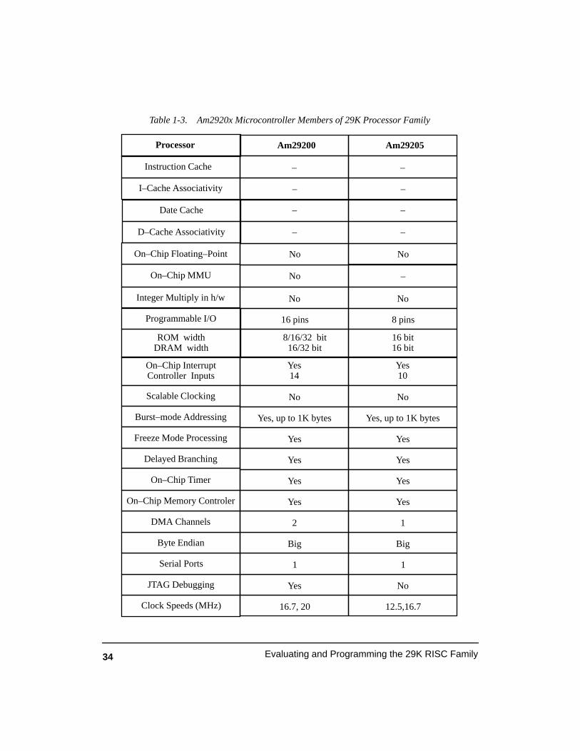
34 Evaluating and Programming the 29K RISC Family
Processor Am29200 Am29205
Programmable I/O 16 pins 8 pins
ROM widthDRAM width
8/16/32 bit16/32 bit
16 bit16 bit
Table 1-3. Am2920x Microcontroller Members of 29K Processor Family
Instruction Cache
I–Cache Associativity
On–Chip Floating–Point
On–Chip MMU
On–Chip InterruptController Inputs
–
–
No
No
Yes14
–
–
No
–
Serial Ports 1 1
Yes10
– –
D–Cache Associativity – –
Integer Multiply in h/w No No
DMA Channels 2 1
Byte Endian Big Big
Scalable Clocking No No
Burst–mode Addressing Yes, up to 1K bytes Yes, up to 1K bytes
Freeze Mode Processing Yes Yes
Delayed Branching Yes Yes
On–Chip Timer Yes Yes
On–Chip Memory Controler Yes Yes
Clock Speeds (MHz) 16.7, 20 12.5,16.7
JTAG Debugging Yes No
Date Cache

35Chapter 1 Architectural Overview
Figure 1-12. Am29200 Microcontroller Address SpaceRegions
video–DRAM
virtual–DRAM
DRAM
ROM
control regs.
reserved
PIA space
Region Allocation Address Range
0xffff,ffff
0x9600,0000
0x9000,0000
0x8000,0000
0x6000,0000
0x5000,0000
0x4000,0000
0x0
(see Figure 1-13). Let’s take a quick look at each of the region controllers and spe-cialized on–chip peripherals in turn.
1.8.1 ROM Region
First thing to realize is that ROM space is really intended for all types ofnonmultiplexed–address devices, such as ROM and SRAM. Controlling access tothese types of memories is very similar. The region is divided into four banks. Eachbank is individually configurable in width and timing characteristics. A bank can beassociated with 8–bit, 16–bit or 32–bit memory and can contain as much as 16Mbytes of memory (enabling a 64M bytes ROM region).
Bank 0, the first bank, is normally attached to ROM memory as code executionafter processor reset starts at address 0. During reset the BOOTW (boot ROM width)input pin is tested to determine the width of Bank 0 memory. Initially the memory isassumed to have 4–cycle access times (three wait states) and no burst–mode. TheSA29200 evaluation board contains an 8–bit EPROM at bank 0 (SA stands for stand–alone). Other banks may contain, say, 32–bit SRAM with different wait state require-ments. It is possible to arrange banks to form a contiguous address range.
Whenever memory in the ROM address range is accessed, the controller for theregion is activated and the required memory chip control signals such as CE (chipenable), R/W, OE (output enable) and others are generated by the microcontroller.Thus SRAM and EPROM devices are wired directly to pins on the microcontrol chip.

36 Evaluating and Programming the 29K RISC Family
Figure 1-13. Am29200 Microcontroller Block Diagram
parallelport
serialport
videointerface
I/Oport
ROMcontroller
DRAMcontroller
DMAcontroller
PIA
interruptcontroller
ROM orSRAM
Memory
DRAM
Memory
Am29000
A I D
1.8.2 DRAM Region
In a way similar to the ROM region, there is a dedicated controller for DRAMdevices which are restricted to being located in the DRAM address region. Onceagain the region is divided into four banks which may each contain as much as 16Mbytes of off–chip memory. The DRAM region controller supports 16–bit or 32–bitwide memory banks which may be arranged to appear as contiguous in addressrange.
DRAM, unlike ROM, is always assumed to have 4–cycle access times. Howev-er, if page–mode DRAM is used it is possible to achieve 2–cycle rather than 4–cycleburst–mode accesses. Burst–mode is used when consecutive memory addresses arebeing accessed, such as during instruction fetching between program branches. TheDRAM memory is often referred to as 3/2 rather than 4/2. The four cycles consist of1-cycle precharge and 3–cycles latency, under certain circumstances the 1–cycle ofprecharge can be hidden. This is explained in section 1.14.1 under the Am29200 andAm29205 subheading.
The control register associated with each DRAM bank, maintains a field forDRAM refresh support. This field indicates the number of processor cycles betweenDRAM refresh. If refresh is not disabled, “CAS before RAS” cycles are performed

37Chapter 1 Architectural Overview
when required. Refresh is overlapped in the background with non–DRAM accesswhen possible.
If a DRAM bank contains video–DRAM rather than conventional DRAM, thenit is possible to perform data transfer to the VDRAM shift register via accesses in theVDRAM address range. The VDRAM is aliased over the DRAM region. Accessingthe memory as VDRAM only changes the timing of memory control signals such asto indicate a video shift register transfer is to take place rather than a CPU memoryaccess.
1.8.3 Virtual DRAM Region
A 16–Mbyte (24 address bit) virtual address space is supported via four map-ping registers. The virtually addressed memory is divided into 64K byte (16 addressbits) memory pages which are mapped into physical DRAM. Each mapping registerhas two 8–bit fields specifying the upper address bits of the mapped memory pages.When memory is accessed in the virtual address space range, and one of the fourmapping registers contains a match for the virtually addressed page being accessed,then the access is redirected to the physical DRAM page indicated by the mappingregister.
When no mapping register contains a currently valid address translation for therequired virtual address, a processor trap occurs. In this case memory managementsupport software normally updates one of the mapping registers with a valid mappingand normal program execution is restarted.
Only DRAM can be mapped into the virtual address space. The address regionsupports functions such as image compression and decompression that yield loweroverall memory requirements and, thus, lower system costs. Images can be stored invirtually addressed space in a compressed form, and only uncompressed into physi-cally accessed memory when required for image manipulation or output video imag-ing.
1.8.4 PIA Region
The Peripheral Interface Adapter (PIA) region is divided into six banks, each of24–bit address space. Each bank can be directly attached to a peripheral device. Thecontrol registers associated with the region give extra flexibility in specifying thetiming for signal pins connecting the microcontroller and PIA peripherals. The PIAdevice–enable and control signals are again provided on–chip rather than in externalsupport circuitry.
When external DMA is utilized, transfer of data is always between DRAM orROM space and PIA space. More on DMA follows.
1.8.5 DMA Controller
When an off–chip device wishes to gain access to the microcontroller DRAM, itmakes use of the Direct Memory Access (DMA) Controller. On–chip peripherals can

38 Evaluating and Programming the 29K RISC Family
also perform DMA transfers; this is referred to as internal DMA. DMA is initiated byan external or internally generated peripheral DMA request.
The only internal peripherals which can generate DMA requests are the parallelport, the serial port and the video interface. These three devices are described shortly.There are two external DMA request pins, one for each of the two on–chip DMA con-trol units. Internal peripherals have a control register field which specifies whichDMA controller their DMA request relates to.
The DMA controllers must be initialized by software before data transfer from,or to, DRAM takes place. The associated control registers specify the DRAM startaddress and the number of transfers to take place. Once the DMA control registershave been prepared, a DMA transfer will commence immediately upon request without any further CPU intervention. Once the DMA transfer is complete the DMA con-troller may generate an interrupt. The processor may then refresh the DMA controlunit parameters for the next expected DMA transfer.
One of the DMA control units has the special feature of having a duplicate set ofDMA parameter registers. At the end of a DMA transfer, when the primary set ofDMA parameter registers have been exhausted, the duplicate set is immediately co-pied into the primary set. This means the DMA unit is instantly refreshed and pre-pared for a further DMA request. Ordinarily the DMA unit is not ready for further useuntil the support software has executed, usually via an end of DMA interrupt request.Just such an interrupt may be generated but it will now be concerned with preparingparameters for the duplicate control registers for the one–after–next DMA request.This DMA queue technique is very useful when DMA transfers are occurring to thevideo controller. In such case DMA can not be postponed as video imaging require-ments mean data must be available if image distortion is to be avoided.
External DMA can only occur between DRAM or ROM space and two of the sixPIA address space banks. DMA only supports an 8–bit address field within a PIA ad-dress bank.
One further note on DMA, the microcontroller does support an external DMAcontroller; enabling random access by the external DMA device to DRAM andROM. The external DMA unit must activate the associated control pins and place theaddress on the microcontroller address bus. In conjunction with the microcontroller,the external DMA unit must complete the single 32–bit data access.
1.8.6 16–bit I/O Port
The I/O port supports bit programmable access to 16 input or output pins. Thesepins can also be used to generate level–sensitive or edge–sensitive interrupts. Whenused as outputs, they can be actively driven or used in open collector mode.
1.8.7 Parallel Port
The parallel port is intended for connecting the microcontroller chip to a hostprocessor, where the controller acts as an intelligent high performance control unit.
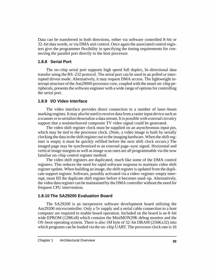
39Chapter 1 Architectural Overview
Data can be transferred in both directions, either via software controlled 8–bit or32–bit data words, or via DMA unit control. Once again the associated control regis-ters give the programmer flexibility in specifying the timing requirements for con-necting the parallel port directly to the host processor.
1.8.8 Serial Port
The on–chip serial port supports high speed full duplex, bi–directional datatransfer using the RS–232 protocol. The serial port can be used in an polled or inter-rupted driven mode. Alternatively, it may request DMA access. The lightweight in-terrupt structure of the Am29000 processor core, coupled with the smart on–chip pe-ripherals, presents the software engineer with a wide range of options for controllingthe serial port.
1.8.9 I/O Video Interface
The video interface provides direct connection to a number of laser–beammarking engines. It may also be used to receive data from a raster input device such asa scanner or to serialize/deserialize a data stream. It is possible with external circuitrysupport that a noninterleaved composite TV video signal could be generated.
The video shift register clock must be supplied on an asynchronous input pin,which may be tied to the processor clock. (Note, a video image is built by seriallyclocking the data in the shift register out to the imaging hardware. When the shift reg-ister is empty it must be quickly refilled before the next shift clock occurs.) Theimaged page may be synchronized to an external page–sync signal. Horizontal andvertical image margins as well as image scan rates are all programmable via the nowfamiliar on–chip control register method.
The video shift registers are duplicated, much like some of the DMA controlregisters. This reduces the need for rapid software response to maintain video shiftregister update. When building an image, the shift register is updated from the dupli-cate support register. Software, possibly activated via a video–register–empty inter-rupt, must fill the duplicate shift register before it becomes used–up. Alternatively,the video data register can be maintained by the DMA controller without the need forfrequent CPU intervention.
1.8.10 The SA29200 Evaluation Board
The SA29200 is an inexpensive software development board utilizing theAm29200 microcontroller. Only a 5v supply and a serial cable connection to a hostcomputer are required to enable board operation. Included on the board is an 8–bitwide EPROM (128Kx8) which contains the MiniMON29K debug monitor and theOS–boot operating system. There is also 1M byte of 32–bit DRAM (256Kx32) intowhich programs can be loaded via the on–chip UART. The processor clock rate is 16

40 Evaluating and Programming the 29K RISC Family
MHz and the DRAM operates with 4–cycle initial access and 2–cycle subsequentburst accesses. So, although the performance is good, it is not as high as other mem-bers of the 29K family.
The SA29200 board measures about 3 by 3.5 inches (9x10 cm) and has connec-tions along both sides which enable attachment to an optional hardware prototypingboard (see following section). This extension board has additional I/O interface de-vices and a small wire–wrap area for inclusion of application specific hardware.
1.8.11 The Prototype Board
The prototying board is inexpensive because it contains mainly sockets, whichcan support additional memory devices, and a predrilled wire–wrap area. The RISCmicrocontroller signals are made available on the prototyping board pins. Some ofthese signals are routed to the empty memory sockets so as to enable simple memoryexpansions for 8–bit, 16–bit or 32–bit EPROM or SRAM. There is also space for upto 16M bytes of 32–bit DRAM.
Using the wire–wrap area the microcontroller I/O signals can be connected todevices supporting specific application tasks, such as A/D conversion or peripheralcontrol. This makes the board ideal for a student project. Additionally, the accesstimes for memory devices are programmable, thus enabling the effects of memoryperformance on overall system operation to be evaluated.
1.8.12 Am29200 Evaluation
The Combination of the GNU tool chain and the low cost SA29200 evaluationboard and associated prototping board, makes available an evaluation environmentfor the industry’s leading embedded RISC. The cost of getting started with embeddedRISC is very low and additional high performance products can be selectively pur-chased from specialized tool builders. The evaluation package should be of particu-lar interest to university undergraduate and post–graduate courses studying RISC.
1.8.13 The Am29205 Microcontroller
The Am29205 is a microcontroller member of the 29K family (see Table 1-3). Itis functionally very similar to the Am29200 microcontroller. It differs as a result ofreduced system interface specifications. This reduction enables a lower device pin–count and packaging cost. The Am29205 is available in a 100–lead Plastic Quad FlatPack (PQFP) package. It is suitable for use in price sensitive systems which can oper-ate with the somewhat reduced on–chip support circuitry.
The reduction in pin count results in a 16–bit data/instruction bus. The processorgenerates two consecutive memory requests to access instructions and data largerthan 16–bits. The memory system interface has also been simplified in other ways.Only 16–bit transfers to memory are provided for; no 8–bit ROM banks are sup-

41Chapter 1 Architectural Overview
ported. The parallel port, DMA controller, and PIA, also now support transfers lim-ited to the 16–bit data width.
Generally the number of service support pins such as: programmable Input/Out-put pins (now 8, 16 for the Am29200 processor); serial communication handshakesignals DTR, DSR; DMA request signals; interrupt request pins; and number of de-coded PIA and memory banks, have all been reduced. The signal pins supporting vid-eo–DRAM and burst–mode ROM access have also been omitted. These omissionsdo not greatly restrict the suitability of the Am29205 microcontroller for many proj-ects. The need to make two memory accesses to fetch instructions, which are not sup-ported by an on–chip cache memory, will result in reduced performance. However,many embedded systems do not require the full speed performance of a 32–bit RISCprocessor.
AMD provides a low cost evaluation board known as the SA29205. The board isstandalone and very like the SA29200 evaluation board; in fact, it will fit with thesame prototype expansion board used by the SA29200. It is provided with a 256kbyte EPROM, organized as 128kx16 bits. The EPROM memory is socket upgradableto 1M byte. There is 512K byte of 16–bit wide DRAM. For debugging purposes, itcan use the MiniMON29K debug monitor utilizing the on–chip serial port.
1.9 THE Am29240 MICROCONTROLLER
The Am29240 is a follow–on to the Am29200 microcontroller (see Table 1-4).It was first introduced in 1993. The Am29240 is a member of the Am2924x familygrouping which offers increased on–chip support and greater processing power. Interms of peripherals the Am29240 has two serial ports in stead of the Am29200’s one.It also has 4 DMA controllers in stead of two.
Unlike the Am29200, all of the Am29240 DMA channels support queued datatransfer. Additionally, fly–by DMA transfers are optionally supported. NormalDMA transfers require a read stage followed by a write stage. The data being trans-ferred is temporarily held in an on–chip buffer after being read. With fly–by DMA theread and write stages occur at the same time. This results in a faster DMA transfer.However, the device being accessed must be able to transfer data at the maximumDRAM access rate.
The Am2924x family grouping, unlike the Am2920x grouping, support virtualmemory addressing. The Translation Look–Aside Buffer (TLB) used to construct anMMU scheme supports larger page sizes than the Am29000 processor. The page sizecan be up to 16M bytes. The large page size enables extensive memory regions to bemapped with only a few TLB mapping entries. For this reason only 16 TLB entriesare provided (8 sets, two entries per set). A consequence of the relatively large pagesize is pages can not be individually protected against Supervisor mode reads andexecution –– this is possible with the smaller pages used by the Am29000 processor(see section 6.2.1). This loss is outweighed by the benefits of the larger page size
42 Evaluating and Programming the 29K RISC Family
Processor Am29240 Am29243
Programmable I/O 16 pins 8 pins
ROM widthDRAM width
8/16/32 bit16/32 bit
16/32 bit8/16/32 bit (parity)
Table 1-4. Am2924x Microcontroller Members of 29K Processor Family
Instruction Cache
I–Cache Associativity
On–Chip Floating–Point
On–Chip MMU
On–Chip InterruptController Input’s
4K bytes
2–Way
No
Yes
Yes14
4K bytes
2–Way
No
Yes
Serial Ports 2 2
Yes14
Data Cache (Physical) 2K bytes 2K bytes
D–Cache Associativity 2–Way 2–Way
Integer Multiply in h/w Yes, 1–cycle Yes, 1–cycle
DMA Channels 4 4
Byte Endian Big Big
Scalable Clocking 1x,2x 1x,2x
Burst–mode Addressing Yes, up to 1K bytes Yes, up to 1K bytes
Freeze Mode Processing Yes Yes
Delayed Branching Yes Yes
On–Chip Timer Yes Yes
On–Chip Memory Controller Yes Yes
Clock Speeds (MHz) 0–20,25,33 0–20,25,33
JTAG Debugging Yes Yes
Am29245
8 pins
8/16/32 bit16/32 bit
4K bytes
2–Way
No
Yes
1
Yes14
–
–
No
2
Big
No
Yes, up to 1K bytes
Yes
Yes
Yes
Yes
0–16
Yes
43Chapter 1 Architectural Overview
which achieves virtual memory addressing with little TLB reload activity and withonly a small amount of chip area being required.
Increased performance is achieved by the inclusion of separate 4k byte instruc-tion and 2k byte data caches. As with all 29K instruction caches, address tags arebased on virtual addresses when address translation is turned on. The first processorin the 29K Family to have a conventional instruction cache was the Am29030. TheAm29240 cache is similar in operation to the Am29030’s cache. However, theAm29240 processor has four valid bits per cache entry (four instructions) in place ofthe previous one bit. This offers a performance advantage as cache blocks need onlybe partially filled and need not be fetched according to block boundaries (more onthis in section 5.13.5).
The data cache always operates with physical addresses. The block size is 16bytes and there is one valid bit per block. This means that compete data blocks mustbe fetched when data cache reload occurs. A “write–through” policy is supported bythe cache which ensures that external memory is always consistent with cache con-tents. Cache blocks are only allocated for data loaded from DRAM or ROM addressregions. Access to other address regions is not cached. A two word write–throughbuffer is used to assist with writes to memory. It enables multiple store instructions tobe in–execution without the processor pipeline stalling. Data accesses which hit inthe cache require 1–cycle access times. The data cache operation is explained in de-tail in section 5.14.
Scalable bus clocking is supported; enabling the processor to run at twice thespeed of the off–chip memory system. Scalable Clocking was first introduced withthe Am29030 processors, and is described in the previous section describing theAm29030. If cache hit rates are sufficiently high, Scalable Clocking enables highperformance systems to be built around relatively slow memory systems. It also of-fers an excellent upgrade path when addition performance is required in the future.
Initially the ROM memory region is assumed to have four cycle access times(three wait states) and no burst–mode –– same as Am29200. The four banks withinthe region can be programmed for zero wait–state read and one wait–state write, oranother combination suitable for slower memory devices.
DRAM, unlike ROM, is always assumed to have 3–cycle access times. Howev-er, if page–mode DRAM is used it is possible to achieve 1–cycle burst–mode ac-cesses. Burst–mode is used when consecutive memory addresses are being accessed,such as during instruction fetching. The Am29200 microcontroller supports 4–cycleDRAM access with 2–cycle burst. The faster DRAM interface of the Am29240should result in a substantial performance gain. Additionally, the 3–cycle initialDRAM access can be reduced to 2–cycle if the required 1–cycle precharge can behidden. This is explained in section 1.14.1 under the Am29200 and Am29205 sub-heading. Consequently the Am29240 DRAM is often referred to as 2/1 rather than3/1.

44 Evaluating and Programming the 29K RISC Family
The Am29240 processor supports integer multiply directly in a single cycle.Most 29K processors take a trap when an integer multiply is attempted. It is left totrapware to emulate the missing instruction. The ability to perform high speed multi-ply makes the processor a better choice for calculation intensive applications such asdigital signal processing. Note, floating–point performance should also improvewith the Am29240 as floating–point emulation routines can make use of the integermultiply instruction.
The Am2924x family grouping is implemented with a silicon process which en-ables processors to operate at 3.3–volts or 5–volts. The lower power consumptionachievable at 3.3–volts makes the Am29240 suitable for hand–held type applica-tions.
1.9.1 The Am29243 Microcontroller
The Am29243 is an Am29240 microcontroller enhanced to deal with commu-nication applications (see Table 1-4). For this reason the video interface is omitted.The pins used have not been reassigned, and there is a possibility they will be allo-cated in a future microcontroller for an additional communications support function.
Communication applications frequently require large amounts of DRAM, and itis often critical that no corruption of the data occur. Parity error checking is often per-formed by memory systems with the objective of detecting data corruption. It can bedifficult to built the necessary circuitry at high memory system speeds. TheAm29243 microcontroller has built–in parity generation and checking for all DRAMaccesses. When enabled by the DRAM controller, the processor will take trap num-ber 4 when a parity error is detected. Having parity handling built–in enables single–cycle DRAM accesses to be performed without any external circuitry required.
Because of the larger amounts of memory typically used in communication ap-plications, the Am29243 has a second Translation Look–Aside Buffer (TLB). Hav-ing two TLBs enables a larger number of virtual to physical address translations to becached (held in a TLB register) at any time. This reduces the TLB reload overhead.The second TLB also has 16 entries (8 sets, two entries per set), and the page size canbe the same or different. If the TLB page sizes are the same, a four–way set associa-tive MMU can be constructed with supporting software. Alternatively one TLB canbe used for code and the second, with a larger page size, for data buffers or sharedlibraries. The TLB entries have a Global Page (GLB) bit; when set the mapped pagecan be accessed by any processes regardless of its process identifier (PID).
1.9.2 The Am29245 Microcontroller
The Am29245 is a low–cost version of the Am29240 microcontroller (seeTable 1-4). To enable the lower cost, the data cache and the integer multiply unit havebeen omitted. Further, there are only two DMA channels in place of the Am29240’sfour. To further reduce cost, one of the two serial ports has also been omitted.
45Chapter 1 Architectural Overview
The Am29245 is intended for use in systems which do not need the maximumperformance of the Am29240 or all of its peripherals; and can benefit from a reducedprocessor cost. The Am29245 does not support Scalable Clocking and is only avail-able at relatively lower clock speeds.
1.9.3 The Am2924x Evaluation
AMD has a number of boards available for Am2924x evaluation. Microcontrol-lers in this family grouping all have the same pin configuration. This enables theboards to operate with any of the Am2924x processors. The least expensive board isthe SD29240 it is a very small board, similar in form to the SA29200 board; it doesnot have the expansion connector available with the SA29200. It is normally sup-plied with an Am29240 or Am29245 installed. There is 1M byte of 32–bit wideDRAM which operates at 16 MHz. When an Am29240 is used, Scalable Clockingcan enable the processor to operate at 32 MHz. The board also has a JTAG andRS–232 connector. The 1M byte of 32–bit wide EPROM supplied with the board ispreprogrammed for MiniMON29K operation.
Those with more money to spend, or requiring a more flexible evaluation board,can use the SE29240 board. It contains an Am29243 processor but can be used toevaluate an Am29240 or Am29245. Initially the board contains 1M byte of 36–bitwide DRAM. However, this can be expanded considerably. The DRAM is 36–bitswide due to the additional 4–bits required for parity checking. The maximummemory speed is 25 MHz. Scalable Clocking can be used with a 32 MHz processorwhen the memory system is configured for 16 MHz operation.
The SE29240 board has greater I/O capability than the SD29240 board. Thereare connectors for two RS–232 ports and a parallel port. Debugging can be achievedvia a serial or parallel port link to the MiniMON29K DebugCore located in EPROM.Debugging is also supported via the JTAG or Logic Analyzer connections. There is asmall wire–wrap area for additional circuitry, and extra boards can be connected viaan expansion connector.
AMD also has an evaluation board intended for certain communication applica-tions. The NET29K board has a triple processor pad–site. The board can operate witheither an Am29205, Am29200 or Am2924x (probably an Am29243) processor. Theprocessor pad site is concentric, the larger processor being at the outer position. Thesimilarity in the memory region controllers enables the construction of this unusualboard.
The memory system consists of 4M bytes of 36–bit wide DRAM, which is ex-pandable. There is also 2M bytes of 32–bit EPROM. The EPROM can be replacedwith 1M byte of Flash programmable memory. For communications there is an AMDMACE chip which provides an Ethernet capability via an 10–Base–T connector. Twoof the processors DMA channels are wired for MACE access. Once channel of an85C30 UART is connected to an RS–449 connector which supports RS–422 signal

46 Evaluating and Programming the 29K RISC Family
level communication. This enables very fast UART communication. The Mini-MON29K DebugCore and OS–boot operating system are initially installed inEPROM (or Flash); and the DebugCore communicates via an on–chip UART con-nected to an RS–232 (9–way) connector.
When the NET29K board is used with an Am29205 processor, the 16–bit pro-cessor bus enables only half of the memory system to be accessed. The board isphysically small, measuring about 5 1/2 x 5 1/2 inches (14cm x 14cm). Debugging isfurther supported by JTAG and Logic Analyzer connections. An inexpensive 9–voltpower supply is required.
1.10 REGISTER AND MEMORY SPACE
Most of the 29K instructions operate on information held in various processorregisters. Load and store type instructions are available for moving data between ex-ternal memory and processor registers. Members of the 29K family generally sup-port registers in three independent register regions which make up the 29K registerspace. These regions are the General Purpose registers, Translation Look–Aside(TLB) registers, and Special Purpose registers. Members of the 29K family which donot support Memory Management Unit operation, do not have TLB registers imple-mented.
There are currently two core processors within the 29K family, the Am29000and the Am29050. Other processors are generally derived from one of these core pro-cessors. For example, the Am29030 has an Am29000 at its core, with additional sili-con area being used to implement instruction cache memory and a 2–bus processorinterface. The differences between the core processors and their derivatives is re-flected in expansions to the special register space.
However, the special register space does appear uniform through out the 29Kfamily. Generally only those concerned with generating operating system supportcode are concerned with the details of the special register space. AMD has specified asubset of special registers which are supported on all 29K family processors. Thisaids in the development and porting of Supervisor mode code.
The core processors support a 3–bus Harvard Architecture, with instructionsand data being held in separate external memory systems. There is one 32–bit buseach for the two memory systems and a shared 32–bit address bus. Some RISC chipshave a 4–bus system, where there is an address bus for each of the two memory sys-tems. This avoids the contention for use of a shared address bus. Unfortunately, it alsoresults in increased pin–count and, consequently, processor cost. The 29K 3–bus pro-cessors avoid conflicts for the address bus by supporting burst mode addressing and alarge number of on–chip registers. It has been estimated that the Am29000 processorlosses only 5% performance as a result of the shared address bus.
All instruction fetches are directed to instruction memory; data accesses are di-rected to data memory or I/O space. These two externally accessible spaces consti-

47Chapter 1 Architectural Overview
tute two of the four external access spaces. The other two are the ROM space and thecoprocessor space. The ROM space is accessed via the instruction bus. Like theinstruction space it covers a 232 range.
1.10.1 General Purpose Registers
All members of the family have general purpose registers which are made upfrom 128 local registers and more than 64 global registers (see Figure 1-14). Theseregisters are the primary source and destination for most 29K instructions. Instruc-tions have three 8–bit operand fields which are used to supply the addresses of gener-al registers. All User mode executable instructions and code produced by high levellanguage compilers, are restricted to only directly assessing general purpose regis-ters. The fact that these registers are all 32–bit and that there is a large number ofthem, vis–a–vis CISC, reduces the need to access data held in external memory.
General purpose registers are implemented by a multiport register file. This filehas a minimum of three access ports, the Am29050 processor has an additional portfor writing–back floating–point results. Two of the three ports provide simultaneousread access to the register file; the third port is for updating a register value. Instruc-tions generally specify two general purpose register operands which are to be oper-ated on. After these operands have been presented to the execution unit, the result ofthe operation is made available in the following cycle. This allows the result of aninteger operation to be written back to the selected general purpose register in thecycle following its execution. At any instant, the current cycle is used to write–backthe result of the previous computation.
The Am29050 can execute floating–point operations in parallel with integeroperations. The latency of floating–point instructions can be more than the 1–cycleachieved by the integer operation unit. Floating–point results are written back, whenthe operation is complete, via their own write–back port, without disrupting the inte-ger units ability to write results into the general purpose register file.
Global Registers
The 8–bit operand addressing fields enable only the lower 128 of the possible256 address values to be used for direct general purpose register addressing. This isbecause the most significant address bit is used to select a register base–plus–offsetaddressing mode. When the most significant bit is zero, the accessed registers areknown as Global Registers. Only the upper 64 of the global registers are implement-ed in the register file. These registers are known as gr64–gr127. Some of the loweraddress–value global registers are assigned special support tasks and are not reallygeneral purpose registers.
The Am29050 processor supports a condition code accumulator with globalregisters gr2 and gr3. The accumulator can be used to concatenate the result of sever-al Boolean comparison operations into a single condition code. Later the accumu-
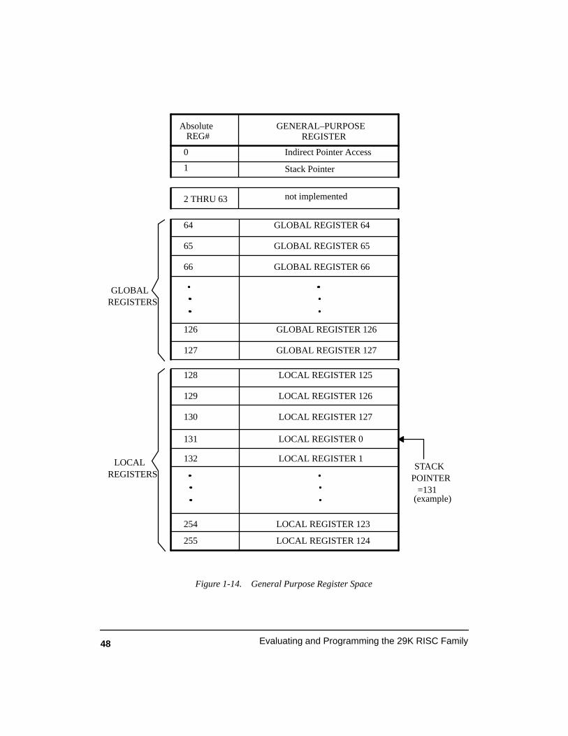
48 Evaluating and Programming the 29K RISC Family
Absolute REG#
GENERAL–PURPOSEREGISTER
0
1 Stack Pointer
Indirect Pointer Access
2 THRU 63 not implemented
64 GLOBAL REGISTER 64
65 GLOBAL REGISTER 65
66 GLOBAL REGISTER 66
126 GLOBAL REGISTER 126
127 GLOBAL REGISTER 127
128 LOCAL REGISTER 125
129 LOCAL REGISTER 126
130 LOCAL REGISTER 127
254 LOCAL REGISTER 123
255 LOCAL REGISTER 124
131 LOCAL REGISTER 0
132 LOCAL REGISTER 1
POINTERSTACK
=131
REGISTERSGLOBAL
LOCALREGISTERS
(example)
Figure 1-14. General Purpose Register Space

49Chapter 1 Architectural Overview
lated condition can be quickly tested. These registers are little used and on the wholeother, more efficient, techniques can be found in preference to their use.
Local Registers
When the most significant address bit is set, the upper 128 registers in the gener-al purpose register file are accessed. The lower 7–bits of the address are used as anoffset to a base register which points into the 128 registers. These general purposeregisters are known as the Local Registers. The base register is located at the globalregister address gr1. If the addition of the 7–bit operand address value and the registerbase value produces a results too big to be contained in the 7–bit local register addressspace, the result is rounded modulo–128. When producing a general purpose registeraddress from a local register address, the most significant bit of the general purposeregister address value is always set.
The local register base address can be read by accessing global register gr1.However, the base register is actually a register which shadows global register gr1.The shadow support circuitry requires that the base be written via an ALU operationproducing a result destined for gr1. This also requires that a one cycle delay followthe setting of the base register and any reference to local registers.
Global register address gr0 also has a special meaning. Each of the three oper-and fields has an indirect pointer register located in the special register space. Whenaddress gr0 is used in an operand field, the indirect pointer is used to access a generalpurpose register for the associated operand. Each of the three indirect pointers has an8–bit field and can point anywhere in the general purpose register space. When indi-rect pointers are used, there is no distinction made between global and local registers.
All of the general purpose registers are accessible to the processor while execut-ing in User mode unless register bank protection is applied. General purpose registersstarting with gr64 are divided into groups of 16 registers. Each group can have accessrestricted to the processor operating in Supervisor mode only. The AMD high levellanguage calling convention specifies that global registers gr64–gr95 be reserved foroperating system support tasks. For this reason it is normal to see the special registerused to support register banking set to disable User mode access to global registersgr64–gr95.
1.10.2 Special Purpose Registers
Special purpose register space is used to contain registers which are not ac-cessed directly by high level languages. Registers such as the program counter andthe interrupt vector table base pointer are located in special register space. Normallythese registers are accessed by operating system code or assembly language helperroutines. Special registers can only be accessed by move–to and move–from typeinstructions; except for the move–to–immediate case. Move–to and move–frominstructions require the use of a general purpose register. It is worth noting that

50 Evaluating and Programming the 29K RISC Family
move–to special register instructions are among a small group of instructions whichcause processor serialization. That is, all outstanding operations, such as overlappingload or store instructions, are completed before the serializing instruction com-mences.
Special register space is divided into two regions (see Figure 1-15). Those reg-isters whose address is below sr128 can only be accessed by the processor operatingin Supervisor mode. Different members of the 29K family have extensions to theglobal registers shown in Figure 1-15. However, special registers sr0–sr14 are a sub-set which appear in all family members. Certain, generally lower cost, family mem-bers such as the Am29005 processor, which have no memory management unit, donot have the relevant MMU support registers (sr13 and sr14). I shall first describe therestricted access, or protected, special registers. I shall not go into the exact bit–fieldoperations in detail, for an expansion of field meanings see later chapters or the rele-vant processor User’s Manual. The objective here is to provide a framework for bet-ter understanding the special register space.
Special registers are not generally known by their special register number. Forexample, the program counter buffer register PC1 is known as PC1 by assembly lan-guage programming tools rather than sr11.
Vector Area BaseSpecial register sr0, better known as VAB, is a pointer to the base of a table of
256 address values. Each interrupt or trap is assigned a unique vector number. Vectornumbers 0–63 are assigned to specific processor support tasks. When an interrupt ortrap exception is taken, the vector number is used to index the table of address values.The identified address value is read and used as the start address of the exceptionhandling routine. Alternatively with 3–bus members of the 29K family, the vectortable can contain 256 blocks of instructions. The VF bit (vector fetch) in the proces-sor Configuration register (CFG) is used to select the vector table configuration.Each block is limited to 64 instructions, but via this method the interrupt handler canbe reached faster as the start of, say, an interrupt handler need not be preceded by afetch of the address of the handler. In practice the table of vectors to handlers, ratherthan handlers themselves, is predominantly used due to the more efficient use ofmemory. For this reason the two later 2–bus members of the 29K family only supportthe table of vectors method; and the VF bit in the CFG register is reserved and effec-tively set.
The first 29K processor, the Am29000, has a VAB register which requires thebase of the vector table to be aligned to a 64k byte address boundary. This can be in-convenient and lead to memory wastage. More recent family members provide for a1k byte boundary. Because the 3–bus family members support instructions being lo-cated in Instruction space and ROM space (memory space is described in section1.10.4), it is possible with these processors to specify that handler routines are inROM space by setting the RV bit (ROM vector area) in the CFG register when the VF

51Chapter 1 Architectural Overview
Special PurposeReg. No. Protected Registers
Old Processor Status
Channel Data
Vector Area Base Address
Current Processor Status
Configuration
Channel Address
Channel Control
Timer Counter
Timer Reload
Register Bank Protect
Program Counter 0
Program Counter 1
LRU Recommendation
Program Counter 2
MMU Configuration
0
1
2
3
4
5
6
7
8
9
10
11
12
13
14
Unprotected Registers
Q
ALU Status
Byte pointer
Funnel Shift Count
Load/Store Count Remaining
128
129
130
131
132133
134
135
Indirect Pointer C
Indirect Pointer A
Indirect Pointer B
Figure 1-15. Special Purpose Register Space for the Am29000 Microprocessor
Floating–Point Environment
Integer Environment
Floating–Point Status
160
161
162
IPC
IPA
IPB
Q
ALUBP
FC
CR
FPE
INTE
FPS
VAB
OPS
CPS
CFG
CHA
CHD
CHC
RBP
TMC
TMR
PC0
PC1
PC2
MMU
LRU
Mnemon-ic

52 Evaluating and Programming the 29K RISC Family
bit is zero. Or, when the more typical table of vectors method is being used by, settingbit–1 of the handler address. Since handler routines all start on 4–byte instructionboundaries, bits 0 and 1 of the vector address are not required to hold address in-formation. The 2–bus and microcontroller members of the 29K family do not supportROM space and RV bit in the CFG registers is reserved.
Processor Status
Two special registers, sr1 and sr2, are provided for processor status reportingand control. The two registers OPS (old processor status) and CPS (current processorstatus) have the same bit–field format. Each bit position has been assigned a uniquetask. Some bit positions are not effective with particular family members. For exam-ple, the Am29030 processor does not use bit position 15 (CA). This bit is used to indi-cate coprocessor activity. Only the 3–bus family members support coprocessor op-eration in this way.
The CPS register reports and controls current processor operation. Supervisormode code is often involved with manipulating this register as it controls the enablingand disabling of interrupts and address translation. When a program execution ex-ception is taken, or an external event such as an interrupt occurs, the CPS registervalue is copied to the OPS register and the processor modifies the CPS register toenter Supervisor mode before execution continues in the selected exception handlingroutine. When returning from the handler routine, the interrupted program is re-started with an IRET type instruction. Execution of an IRET instruction causes theOPS register to be copied back to the CPS register, helping to restore the interruptedprogram context. Supervisor mode code often prepares OPS register contents beforeexecuting an IRET and starting User mode code execution.
Configuration
Special register sr3, known as the configuration control register (CFG), esta-blishes the selected processor operation. Such options as big or little endian byte or-der, cache enabling, coprocessor enabling, and more are selected by the CFG setting.Normally this register value is established at processor boot–up time and is infre-quently modified.
The original Am29000 (rev C and later) only used the first six bits of the CFGregister for processor configuration. Later members of the family offer the selectionof additional processor options, such as instruction memory cache and early addressgeneration. Additional options are supported by extensions to the CFG bit–field as-signment. Because there is no overlap with CFG bit–field assignment across the 29Kfamily, and family members offer a matrix of functionality, there are often reservedbit–fields in the CFG register for any particular 29K processor. The function pro-vided at each bit position is unique and if the function is not provided for by a proces-sor, the bit position is reserved.
53Chapter 1 Architectural Overview
The upper 8–bits of the CFG register are used for processor version and revisionidentification. The upper 3–bits of this field, known as the PRL (processor revisionlevel) identify the processor. The Am29000 processor is identified by processornumber 0, the Am29050 is processor number 1, and so on. The lower 5–bits of thePRL give the the revision level; a value of 3 indicates revision ‘D’. The PRL field isread–only.
Data Access ChannelThree special registers, sr4–sr6, known as CHA (channel address), CHD (chan-
nel data) and CHC (channel control), are used to control and record all access to ex-ternal data memory. Processors in the 29K family can perform data memory access inparallel with instruction execution. This offers a considerable performance boost,particularly where there is high data memory access latency. Parallel operation canonly occur if the instruction pipeline can be kept fed from the instruction prefetchbuffer (IPB), instruction memory cache, or via separate paths to data and instructionmemory (Harvard style 3–bus processors). It is an important task of a high level lan-guage compiler to schedule load and store instructions such that they can be success-fully overlapped with other nondependent instructions (see section 1.13).
When data memory access runs in parallel, its completion will occur some timeafter the instruction originally making the data access. In fact it could be severalcycles after the original request, and it may not be possible to determine the originalinstruction. On many processors, keeping track of the original instruction is requiredin case the load or store operation does not complete for some reason. The originalinstruction is restarted after the interrupting complication has been dealt with. How-ever, with the 29K family the original instruction is not restarted. All access to exter-nal memory is via the processor Data Channel. The three channel support registersare used to restart any interrupted load or store operation. Should an exception occurduring data memory access, such as an address translation fault, memory accessviolation, or external interrupt, the channel registers are updated by the processor re-porting the state of the in–progress memory access.
The channel control register (CHC) contains a number of bit–fields. The con-tents–valid bit (CV) indicates that the channel support registers currently describe avalid data access. The CV bit is normally seen set when a channel operation is inter-rupted. The ML bit indicates a load– or store–multiple operation is in progress.LOADM and STOREM instructions set this bit when commencing and clear it whencomplete. It is important to note that non–multiple LOAD and STORE instructionsdo not set or clear the ML bit. When a load– or store–multiple operation is interruptedand nested interrupt processing is supported, it is not sufficient to just clear the CV bitto temporary cancel the channel operation. If the ML bit was left set, a subsequentload or store operation would become confused with a multiple type operation. TheML bit should be cleared along with the CV bit; this is best done by writing zero intothe CHC register. (See section 4.3.8 for more information about clearing CHC.)
54 Evaluating and Programming the 29K RISC Family
Integer operations complete in a single cycle, enabling the result of the previousinteger operation to be written back to the general purpose register file in the currentcycle. Because external memory reads are likely to take several cycles to complete,and pipeline stalling is to be avoided, the accessed data value is not written back to theglobal register file during the following instruction (the write–back cycle). This re-sults in the load data being held by the processor until access to the write–back port isavailable. This is certain to occur during the execution of any future load or storeinstruction which itself can not make use of its own write–back cycle. The processormakes available via load forwarding circuitry the load data which awaits write–backto the register file.
Register Access ProtectionSpecial register sr7, known as RBP (register bank protect), provides a means to
restrict the access of general purpose registers by programs executing in User mode.General purpose registers starting with gr64 are divided into groups of 16 registers.When the corresponding bit in the RBP register is set, the associated bank of 16 regis-ters is protected from User mode access. The RBP register is typically used to preventUser mode programs from accessing Supervisor–maintained information held inglobal registers gr64–gr95. These registers are reserved by the AMD high level lan-guage calling convention for system level information.
On–Chip Timer ControlSpecial registers sr8 and sr9, known as TMC (timer counter) and TMR (timer
reload value), support a 24–bit real–time clock. The TMC register decrements at therate of the processor clock. When it reaches zero it will generate an interrupt if en-abled. In conjunction with support software these two registers can be used to imple-ment many of the functions often supported by off–chip timer circuitry.
Program CounterA 29K processor contains a Master and Slave PC (program counter) address
register. The Master PC register contains the address of the instruction currently be-ing fetched. The Slave contains the next sequentional instruction. Once an instruc-tion flows into the execution unit, unless interrupted, the following instruction, cur-rently in decode, will always flow into the execution unit. This is true for all instruc-tions except for instructions such as IRET. Even if the instruction in execute is ajump–type, the following instruction known as the delay–slot instruction is executedbefore the jump is taken. This is known as delayed branching and can be very usefulin hiding memory access latencies, as the processor pipeline can be kept busy execut-ing the delay–slot instruction while the new instruction sequence is fetched. It is animportant activity of high level language compilers to find useful instructions toplace in delay–slot locations.
The Master PC value flows along the PC–bus and the bus activity is recorded bythe PC buffer registers, see Figure 1-16. There are three buffer registers arranged in

55Chapter 1 Architectural Overview
sequence. These buffer registers are accessible within special registers’ space assr10–sr12, better known as PC0, PC1 and PC2. The PC0 register contains the addressof the instruction currently in decode; register PC1 contains the address of theinstruction currently in execute; and PC2 the instruction now in write–back.
InstructionFetch
orCache
30–bitIncrementer
Slave PC
PC MUX
B–BUS, supplies branch addresses
Branch
PC–BUS
PC 0
PC 1Master PC
ReturnAddress
R–BUS
AddressGeneration
Unit30
PC 2
Fetch address
Decode-address
Executeaddress
Write–Backaddress
Figure 1-16. Am29000 Processor Program Counter
PC–Buffer
When a program exception occurs the PC–buffer registers become frozen. Thisis signified by the FZ bit in the current processor status register being set. When fro-zen, the PC–buffer registers accumulate no new PC–bus information. The frozen PCinformation can be used later to restart program execution. An IRET instructioncauses the PC1 and PC0 register information to be copied to the Master and Slave PCregisters and instruction fetching to commence. For this reason it is important tomaintain both PC1 and PC0 values when dealing with such system level activities asnested interrupt servicing. Since the PC2 register records the address of a nowexecuted instruction, maintenance of its value is less important; but it can play an im-portant role in debugging
When a CALL instruction is executed, the B–bus supplies the Master PC withthe address of the new instruction stream. Earlier, when the CALL instruction en-tered the decode stage, the PC–bus was used to fetch the delay–slot instruction; andthe address of the instruction following the delay–slot (the return address) was pre-pared for entry into the Slave PC. On the following cycle, the CALL instruction en-
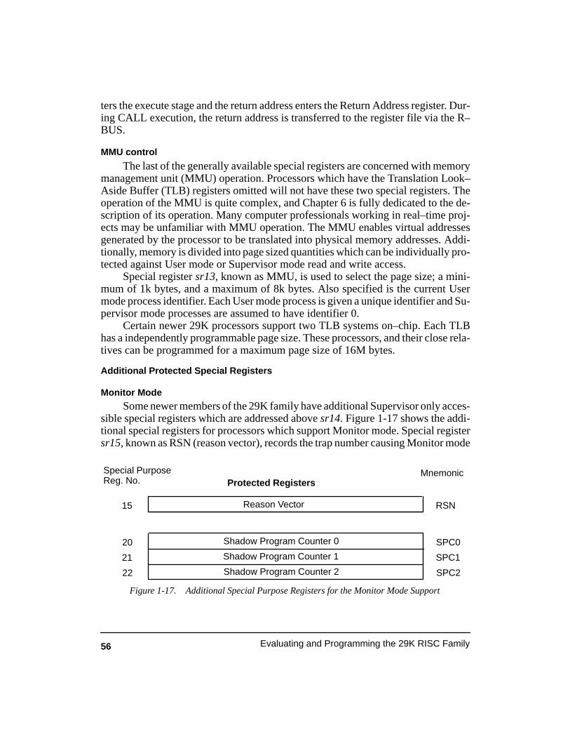
56 Evaluating and Programming the 29K RISC Family
ters the execute stage and the return address enters the Return Address register. Dur-ing CALL execution, the return address is transferred to the register file via the R–BUS.
MMU control
The last of the generally available special registers are concerned with memorymanagement unit (MMU) operation. Processors which have the Translation Look–Aside Buffer (TLB) registers omitted will not have these two special registers. Theoperation of the MMU is quite complex, and Chapter 6 is fully dedicated to the de-scription of its operation. Many computer professionals working in real–time proj-ects may be unfamiliar with MMU operation. The MMU enables virtual addressesgenerated by the processor to be translated into physical memory addresses. Addi-tionally, memory is divided into page sized quantities which can be individually pro-tected against User mode or Supervisor mode read and write access.
Special register sr13, known as MMU, is used to select the page size; a mini-mum of 1k bytes, and a maximum of 8k bytes. Also specified is the current Usermode process identifier. Each User mode process is given a unique identifier and Su-pervisor mode processes are assumed to have identifier 0.
Certain newer 29K processors support two TLB systems on–chip. Each TLBhas a independently programmable page size. These processors, and their close rela-tives can be programmed for a maximum page size of 16M bytes.
Additional Protected Special Registers
Monitor Mode
Some newer members of the 29K family have additional Supervisor only acces-sible special registers which are addressed above sr14. Figure 1-17 shows the addi-tional special registers for processors which support Monitor mode. Special registersr15, known as RSN (reason vector), records the trap number causing Monitor mode
Special PurposeReg. No. Protected Registers
Figure 1-17. Additional Special Purpose Registers for the Monitor Mode Support
Reason Vector15 RSN
Mnemonic
Shadow Program Counter 020 SPC0
Shadow Program Counter 121 SPC1
Shadow Program Counter 222 SPC2

57Chapter 1 Architectural Overview
to be entered. Monitor mode extends the software debugging capability of the pro-cessor; it was briefly described in the previous section describing the processor fea-tures, and is dealt with in detail in later chapters. The shadow Program Counter regis-ters constituted a second set of PC–buffer registers. They record the PC–bus activityand are used to support Monitor mode debugging.
Am29050
Figure 1-18 shows the additional special registers used by the Am29050 pro-cessor for region mapping. In the Am29050 case, the additional special registers sup-port two functions: debugging and region mapping. Four special registers in therange sr16–sr19 extend the virtual address mapping capabilities of the TLB registers.They support the mapping of two regions which are of programmable size. Their usereduces the demand placed on TLB registers to supply all of a systems address map-ping and memory access protection requirements.
Special PurposeReg. No. Protected Registers
Figure 1-18. Additional Special Purpose Registers for the Am29050 Microprocessor
Mnemonic
Region Mapping Address 016 RMA0
Region Mapping Control 017 RMC0
Region Mapping Address 118 RMA1
Region Mapping Control 119 RMC1
Instruction and Data Breakpoints
Figure 1-19 shows the additional special registers for processors which supportbreakpoint debugging. They facilitate the control of separate instruction access
Special PurposeReg. No. Protected Registers
Figure 1-19. Additional Special Purpose Registers for Breakpoint Control
Mnemonic
Data Breakpoint Address 027 DBA0
Date Breakpoint Control 028 DBC0
Instruction Breakpoint Address 023 IBA0
Instruction Breakpoint Control 024 IBC0
Instruction Breakpoint Address 125
Instruction Breakpoint Control 126
IPA1
IBC1

58 Evaluating and Programming the 29K RISC Family
breakpoints and data access breakpoints. Some 29K processors have instructionbreakpoints only; others support both types of breakpoint.
On–Chip Cache Control
Figure 1-20 shows the additional special registers required to access on–chipcache. There are only two additional registers, sr29 and sr30, required. Both registersare used for communicating with the instruction memory cache supported by many29K processors. If a processor also contains data cache, the memory can similarly beaccessed via the same cache interface registers. Supervisor mode support code con-trols cache operation via the processor configuration register (CFG), and is not likelyto make use of the cache interface registers. These registers may be used by debug-gers and monitors to preload and examine cache memory contents.
Special PurposeReg. No. Protected Registers
Figure 1-20. Additional Special Purpose Registers for On–Chip Cache Control
Cache Interface Register29 CIR
Mnemonic
Cache Data Register30 CDR
User Mode Accessible Special Registers
Figure 1-15 showed the special register space with its two regions. The regionaddressed above sr128 is always accessible; and below sr128, registers are only ac-cessible to the processor when operating in Supervisor mode.
The original Am29000 processor defined a subset of User mode accessible reg-isters, in fact those shown in Figure 1-15. Every 29K processor supports the use ofthese special registers, but, only the Am29050 has the full complement implemented.
Registers in the range sr128–sr135 are always present. However, the three reg-isters sr160–sr162 are used to support floating–point and integer operations. Onlycertain members of the 29K family directly support these operations in processorhardware. Other 29K family members virtualize these three registers. When notavailable, an attempt to access them causes a protection violation trap. The trap han-dler identifies the attempted operation and redirects the access to shadow copies ofthe missing registers. The accessor is unaware that the virtualization has occurred,accept for the delay in completing the requested operation. In practice, floating–pointsupporting special registers are not frequently accessed; except for the case of float-ing–point intensive systems which tend to be constructed around an Am29050 pro-cessor.

59Chapter 1 Architectural Overview
Indirect Pointers
Special registers sr128–sr130, better known as IPA, IPB and IPC, are the indi-rect pointers used to access the general purpose register file. For instructions whichmake use of the three operand fields, RA, RB and RC, to address general purposeregisters, the indirect pointer can be used as an alternative operand address source.For example, the RA operand field supplies the register number for the source oper-and–A; if global register address gr0 is used in the RA instruction field, then the oper-and register number is provided by the IPA register.
The IPA, IPB and IPC registers are pointers into the global register file. They aregenerally used to point to parameters passed to User mode helper routines. They arealso used to support instruction emulation, where trap handler routines perform insoftware the missing instruction. The operands for the emulated instruction arepassed to the trap handler via the indirect pointers.
ALU Support
Special registers sr131–sr134 support arithmetic unit operation. Registersr131, better known as Q, is used during floating–point and integer multiply and di-vide steps. Only the Am29050 processor can perform floating–point operations di-rectly, that is, without coprocessor or software emulation help. It is also the only pro-cessor which directly supports integer multiply. All other current members of the29K family perform these operations in a sequence of steps which make use of the Qregister.
The result of a comparison instruction is placed in a general purpose register, aswell as in the condition field of the ALU status register (special register sr132). How-ever, the ALU status register is not conveniently tested by such instructions as condi-tional branch. Branch decisions are made on the basis of True or False values held ingeneral purpose registers. This makes a lot of sense, as contention for use of a singleresource such as the ALU status register would lead to a resource conflict whichwould likely result in unwanted pipeline stalling.
The ALU status register controls and reports the operation of the processor inte-ger operation unit. It is divided into a number of specialized fields which, in somecases, can be more conveniently accessed via special registers sr134 and sr135. Theshort hand access provided by these additional registers avoids the read, shift andmask operations normally required before writing to bit–fields in the ALU register.
Data Access Channel
The three channel control registers, CHA, CHD and CHC, were previously de-scribed in the protected special registers section. However, User mode programshave a need to establish load– and store–multiple operations which are controlled bythe channel support registers. Special register sr135, known as CR, provides a meansfor a User mode program to set the Count Remaining field of the protected CHC reg-ister. This field specifies the number of consecutive words transferred by the multiple
60 Evaluating and Programming the 29K RISC Family
data move operation. Should the operation be interrupted for any reason, the CR fieldreports the number of transfers yet to be completed. Channel operation is typicallyrestarted (if enabled) when an IRET type instruction is issued.
Instruction Environment Registers
Special registers sr160 and sr162, known as FPE and FPS, are the floating–point environment and status registers. The environment register is used by Usermode programs to establish the required floating–point operations, such as double–or single–precision, IEEE specification conformance, and exception trap enabling.The status register reports the outcome of floating–point operations. It is typicallyexamined as a result of a floating–point operation exception occurring. Only proces-sors (Am29050) which support floating–point operations directly (free of trapware)have real sr161 and sr162 registers. All other processors appear to have these regis-ters via trapware support which creates virtual registers.
The integer environment is established by setting special register sr161, knownas INTE. There are two control bits which separately enable integer and multiplica-tion overflow exceptions. If exception detection is enabled, the processor will takean Out–of–Range trap when an overflow occurs. Only processors (Am29040,Am29240 and Am29243) which support integer multiply directly (free of trapware)have a real sr161 register. All other processors appear to have an sr161 register viatrapware support.
Additional User Mode Special Registers
Am29050
The Am29050 has an additional special register, shown in Figure 1-21. Registersr164, known as EXOP, reports the instruction operation code causing a trap. It isused by floating–point instruction exceptions. Unlike other 29K processors theAm29050 directly executes all floating–point instructions. Exception traps can oc-cur during these operations. When instruction emulation techniques are being used, itis an easy matter to determine the instruction being emulated at the time of the trap.However, with direct execution things are not as simple. The processor could ex-amine the memory at the address indicated by the PC–buffer registers to determinethe relevant instruction opcode. But the Am29050 supports a Harvard memory archi-tecture and there is no path within the processor to access the instruction memory as ifit were data. The EXOP register solves this problem. Whenever an exception trap istaken, the EXOP register reports the opcode of the instruction causing the exception.
Users of other 3–bus Harvard type processors such as the Am29000 andAm29005 should take note; virtualizing the unprotected special registers sr160–162requires that the instruction space be readable by the processor (virtualizing, in thiscase, means making registers sr160–162 appear to be accessible even when they arenot physically present). This can only be achieved by connecting the instruction and

61Chapter 1 Architectural Overview
Special PurposeReg. No.
Figure 1-21. Additional Special Purpose Register for the Am29050 Microprocessor
MnemonicUnprotected Registers
Exception Opcode164 EXOP
data busses together (disabling the Harvard architecture advantages by creating a2–bus system) or providing an off–chip bridge. This bridge must enable the addressspace to be reached from within some range of data memory space, at least for word–size read accesses, and, all be it, with additional access time penalties.
The Am29050 processor has an additional group of registers known as the float-ing–point accumulators. There are four 64–bit accumulators ACC3–0 which can beused with certain floating–point operations. They can hold double– or single–preci-sion numbers. They are not special registers in the sense they lie in special registerspace. They are located in their own register space, giving the Am29050 one moreregister space than the normal three register spaces of the other 29K family members.However, like special registers, they can only be accessed by move–to and move–from accumulator type instructions.
Double–precision numbers (64–bit) can be moved between accumulators andgeneral registers in a single cycle. Global registers are used in pairs for this operation.This is possible because the Am29050 processor is equipped with an additional64–bit write–back port for floating point data, and the register file is implementedwith a width of 64–bits.
1.10.3 Translation Look–Aside Registers
Although some 29K family members are equipped with region mapping regis-ters, a Translation Look–Aside Buffer (TLB) technique is generally used to providevirtual to physical address translation. The TLB is two–way set associative and up to64 translations are cached in the TLB support registers.
The TLB registers form the basis for implementing a Memory ManagementUnit. The scheme for reloading TLB registers is not dictated by processor micorcode,but left to the programmer to organize. This enables a number of performance boost-ing schemes to be implemented with low overhead costs. However, it does place theburden of creating a TLB maintenance scheme on the user. Those used to having towork around a processor’s microcode imposed scheme will appreciate the freedom.
TLB registers can only be accessed by move–to TLB and move–from TLBinstructions executed by the processor operating in Supervisor mode. Each of thepossible 64 translation entries (less than 64 with some 29K family members) requires

62 Evaluating and Programming the 29K RISC Family
a pair of TLB registers to fully describe the address translation and access permis-sions for the mapped page. Pages are programmable in size from 1k bytes to 8k bytes(to 16M byte with newer 29K processors), and separate read, write and execute per-missions can be enabled for User mode and Supervisor mode access to the mappedpage.
There is only a single 32–bit virtual address space supported. This space ismapped to real instruction, data or I/O memory. Address translation is performed in asingle cycle which is overlapped with other processor operations. This results in theuse of an MMU not imposing any run–time performance penalties, except whereTLB misses occur and the TLB cache has to be refilled. Each TLB entry is taggedwith a per–process identifier, avoiding the need to flush TLB contents when a user–task context switch occurs. Chapter 6 fully describes the operation of the TLB.
1.10.4 External Address Space
The 3–bus members of the 29K family support five external 32–bit addressspaces. They are:
Data Memory — accessed via the data bus.
Input/Output — also accessed via the data bus.
Instruction — accessed via the instruction bus, normally read–only.
ROM — also accessed via the instruction bus, normally read–only.
Coprocessor — accessed via both data and address busses. Note, the addressbus is only used for stores to coprocessor space. This enables 64–bit transfersduring stores and 32–bit during loads.The address bus is used for address information when accessing all address
spaces except the coprocessor space. During load and store operations to coprocessorspace, address information can be supplied in a limited way by the OPT2–0 field ofthe load and store instructions. Of course, with off–chip address decoding support,access to coprocessor space could always be made available via a region of I/O ordata space. Coprocessors support off–chip extensions to a processor’s executionunit(s). AMD supplied a coprocessor in the past, which was for floating–point sup-port, the Am29027. It is possible that users could construct their own coprocessor forsome specialized support task.
Earlier sections discussed the read–only nature of the instruction bus of 3–busprocessors. Instructions are fetched along the instruction bus from either the ROMspace or the Instruction space. Access to the two 32–bit spaces is distinguished by theIREQT processor pin. The state of this pin is determined by the RE (ROM enable) bitof the current processor status register (CPS). This bit can be set by software or viaprogrammed event actions, such as trap processing. ROM space is intended for sys-tem level support code. Typically systems do not decode this pin and the two spacesare combined into one.

63Chapter 1 Architectural Overview
The Input/Output (I/O) space can be reached by setting the AS (address space)bit in load and store instructions. Transfers to I/O space, like coprocessor space anddata space transfers, are indicated by the appropriate value appearing on theDREQT1–0 (data request type) processor pins. I/O space access is only convenientfor assembly level routines. There is typically no convenient way for a high level lan-guage to indicate an access is to be performed to I/O space rather than data space. Forthis reason use of I/O space is often best avoided, unless it is restricted to accessingsome Supervisor maintained peripheral which is best handled via assembly languagecode.
The 2–bus 29K family processors support a reduced number of off–chip addressspaces, in fact, only two: Input/Output space, and a combined Instruction/Datamemory space. Accessing both instructions and data via a shared instruction/data bussimplifies the memory system design. It can also simplify the software; for example,instruction space and data space can no longer overlap. Consider a 3–bus systemwhich has physical memory located at address 0x10000 in instruction space and alsodifferent memory located at address 0x10000 in data space. Software errors can oc-cur regarding accessing the correct memory for address 0x10000. It can also compli-cate system tasks such as virtual memory management, where separate free–pagelists would have to be kept for the different types of memory.
The Translation Look–Aside buffer (TLB), used to support virtual memory ad-dressing, supports separate enabling of data and instruction access via the R/W/X(read/write/execute) enable bits. However, permission checking is only performedafter address translation is performed. It is not possible to have two valid virtual–to–physical address translations present in the TLB at the same time for the same virtualaddress, even if one physical address is for data space and the other instruction space.This complicates accessing overlapping address spaces via a single 32–bit virtualspace.
Accessing virtual memory has similar characteristics to accessing memory via ahigh level language. For example, C normally supports a single address space. It isdifficult and nonportable to have C code which can reach different address spaces.Except for instruction fetching, all off–chip memory accesses are via load and storetype instructions. The OPT2–0 field for these instructions specifies the size of thedata being transferred: byte, half–word or 32–bit. The compiler assigns OPT fieldvalues for all load and store instructions it generates. Unless via C language exten-sions or assembly code post–processing, there is no way to set the load and storeinstruction address–space–selecting options. Software is simplified by locating allexternal peripherals and memory in a single address space; or when a Harvard archi-tecture is used, by not overlapping the regions of data and instruction memory spacesused.

64 Evaluating and Programming the 29K RISC Family
1.11 INSTRUCTION FORMAT
All instructions for the Am29000 processor are 32 bits in length, and are dividedinto four fields, as shown in Figure 1-22. These fields have several alternative defini-tions, as discussed below. In certain instructions, one or more fields are not used, andare reserved for future use. Even though they have no effect on processor operation,bits in reserved fields should be 0 to insure compatibility with future processor ver-sions.
Op
RCI17..I10
I15..I8VN
CE//CNTL
RASA
I9..I2RB or I
I7..I0
RB
31 23 15 7 0
UI//RND//FD//FS
Figure 1-22. Instruction Format
A//M
The instruction fields are defined as follows:
BITS 31–24Op This field contains an operation code, defining the operation to be
performed. In some instructions, the least–significant bit of the op-eration code selects between two possible operands. For this reason,the least–significant bit is sometimes labeled “A” or “M”, with thefollowing interpretations:
A (Absolute): The A bit is used to differentiate between Program–Counter relative (A = 0) and absolute (A = 1) instruction addresses,when these addresses appear within instructions.
M (IMmediate): The M bit selects between a register operand (M = 0)and an immediate operand (M =1), when the alternative is allowed byan instruction.
BITS 23–16RC The RC field contains a global or local register–number, which is the
destination operand for many instructions.I17..I10 This field contains the most–significant 8 bits of a 16–bit instruction
address. This is a word address, and may be Program–Counter rela-tive or absolute, depending on the A bit of the operation code.

65Chapter 1 Architectural Overview
I15..I8 This field contains the most–significant 8 bits of a 16–bit instructionconstant.
VN This field contains an 8–bit trap vector number.CE//CNTL This field controls a load or store access.
BITS 15–8RA The RA field contains a global or local register–number, which is a
source operand for many instructions.SA The SA field contains a special–purpose register–number.
BITS 7–0RB The RB field contains a global or local register–number, which is a
source operand for many instructions.RB or I This field contains either a global or local register–number, or an
8–bit instruction constant, depending on the value of the M bit of theoperation code.
I9..I2 This field contains the least–significant 8 bits of a 16–bit instructionaddress. This is a word address, and may be Program–Counter rela-tive, or absolute, depending on the A bit of the operation code.
I7..I0 This field contains the least–significant 8 bits of a 16–bit instructionconstant.
UI//RND//FD//FSThis field controls the operation of the CONVERT instruction.
The fields described above may appear in many combinations. However, cer-tain combinations which appear frequently are shown in Figure 1-23.
1.12 KEEPING THE RISC PIPELINE BUSY
If the external interface of a microprocessor can not support an instructon fetchrate of one instruction per cycle, execution rates of one per cycle can not be sustained.As described in detail in Chapter 6, a 4–1 DRAM (4–cycle first access, 1–cycle sub-sequent burst–mode access) memory system used with a 3–bus Am29000 processor,can sustain an average processing time per instruction of typically two cycles, not thedesired 1–cycle per instruction. However, a 2–1 SRAM based system comes veryclose to this target. From these example systems it can be seen that even if a memorysystem can support 1–cycle burst–mode access, there are other factors which preventthe processor from sustaining single–cycle execution rates.
It is important to keep the processor pipeline busy doing useful work. Pipelinestalling is a major source of lost processor performance. Stalling occurs as a result of:

66 Evaluating and Programming the 29K RISC Family
31 23 15 7 0
X X X X X X X 1 I15..I8 RA I7..I0
31 23 15 7 0
X A I17..I10 RA I9..I2
31 23 15 7 0
X X X X X X X M VN RA RB or I
31 23 15 7 0
M CNTL RA RB or I
31 23 15 7 0
X X X X X X X M RC RA RB or I
31 23 15 7 0
X X X X X X X 0 RC RA RB
CE
Three operands, with possible 8–bit constant:
Three operands, without constant::
One register operand, with 16–bit constant:
Jumps and calls with 16–bit instruction address:
Two operands with trap vector number:
Loads and stores:
X X X X X X
X X X X X X X
Figure 1-23. Frequently Occurring Instruction–Field Uses
67Chapter 1 Architectural Overview
inadaquate memory bandwidth, high memory access latency, bus access contention,excesive program branching, and instruction dependancies. To get the best from aprocessor an understanding of instruction stream dependancies is required. Proces-sors in the 29K familiy all have pipeline interlocks supported by processor hardware.The programmer does not have to ensure correct pipeline operation, as the processorwill take care of any dependancies. However, it is best that the programmer arrangescode execution to smooth the pipeline operation.
1.13 PIPELINE DEPENDENCIES
Modification of some registers has a delayed effect on processor behavior.When developing assembly code, care must be taken to prevent unexpected behav-ior. The easiest of the delayed effects to remember is the one cycle that must followthe use of an indirect pointer after having set it. This occurs most often with the regis-ter stack pointer. It cannot be used to access a local register in the instruction that fol-lows the instruction that writes to gr1. An instruction that does not require gr1 (andthat means all local registers referenced via gr1) can be placed immediately after theinstruction that updates gr1.
Direct modification of the Current Processor Status (CPS) register must also bedone carefully. Particularly where the Freeze (FZ) bit is reset. When the processor isfrozen, the special-purpose registers are not updated during instruction execution.This means that the PC1 register does not reflect the actual program counter value atthe current execution address, but rather at the point where freeze mode was entered.When the processor is unfrozen, either by an interrupt return or direct modification ofthe CPS, two cycles are required before the PC1 register reflects the new executionaddress. Unless the CPS register is being modified directly, this creates no problem.
Consider the following examples. If the FZ bit is reset and trace enable (TE) isset at the same time, the next instruction should cause a trace trap, but the PC–bufferregisters frozen by the trap will not have had time to catch up with the current execu-tion address. Within the trap code the processor will have appeared to have stopped atsome random address, held in PC1. If interrupts and traps are enabled at the sametime as the FZ bit is cleared, then the next instruction may suffer an external interruptor an illegal instruction trap. Once again, the PC–buffer register will not reflect thetrue execution address. An interrupt return would cause execution to commence at arandom address. The above problems can be avoided by resetting FZ two cycles be-fore enabling the processor to once again enter freeze mode.
Instruction Memory LatencyThe Branch Target Cache (BTC), or the Instruction Memory Cache, can be used
to remove the pipeline stalling that normally occurs when the processor executes abranch instruction. For the purpose of illustrating memory access latency, the effectsof the BTC shall be illustrated. The address of a branch target appears on the address

68 Evaluating and Programming the 29K RISC Family
pins at the start of the write-back stage. Figure 1-24 shows the instruction flowthrough the pipeline stages, assuming the external instruction memory returns thetarget of a jump during the same cycle in which it was requested. This makes the Tar-get instruction available at the fetch stage while the Delay instruction has to be stalledbefore it can enter the execute stage. In this case, execution is stalled for two cycleswhen the BTC is not used to supply the target instruction.
DelayInstructionFetch
InstructionDecode
InstructionExecution
ResultWrite-Back
Am29000PipelineStages
Jump
Current
Delay
Delay
Delay
Jump
Jump
Target
Target
Target
Target+2Target+1
Target+1
Current Processorcycle
Target = Target of jump instructionLegend: Delay = Delay instruction
futurecycles
Figure 1-24. Pipeline Stages for BTC Miss
1–cycle fetch
Jump = Jump instructionCurrent = Current instruction
= Pipeline stall
Target + 1 = 1st instruction after targetTarget + 2 = 2nd instruction after target
The address of the fetch is presented to the BTC hardware during the executestage of the jump instruction, the same time the address is presented to the memorymanagement unit. When a hit occurs, the target instruction is presented to the decodestage at the next cycle. This means no pipeline stalling occurs. The external instruc-tion memory has up to three cycles to return the instruction four words past the targetaddress. That is, if single-cycle burst–mode can be established in three cycles (fourcycles for the Am29050 processor) or less, then continuous execution can beachieved. The BTC supplies the target instructions and the following three instruc-tions, assuming another jump is not taken. Figure 1-25 shows the flow of instruc-tions through the pipeline stages.
Data Dependencies
Instructions that require the result of a load should not be placed immediatelyafter the load instruction. The Am29000 processor can overlap load instructions withother instructions that do not depend on the result of the load. If 4-cycle data memoryis in use, then external data loads should (if possible) have four instructions(4-cycles) between the load instructions and the first use of the data. Instructions that
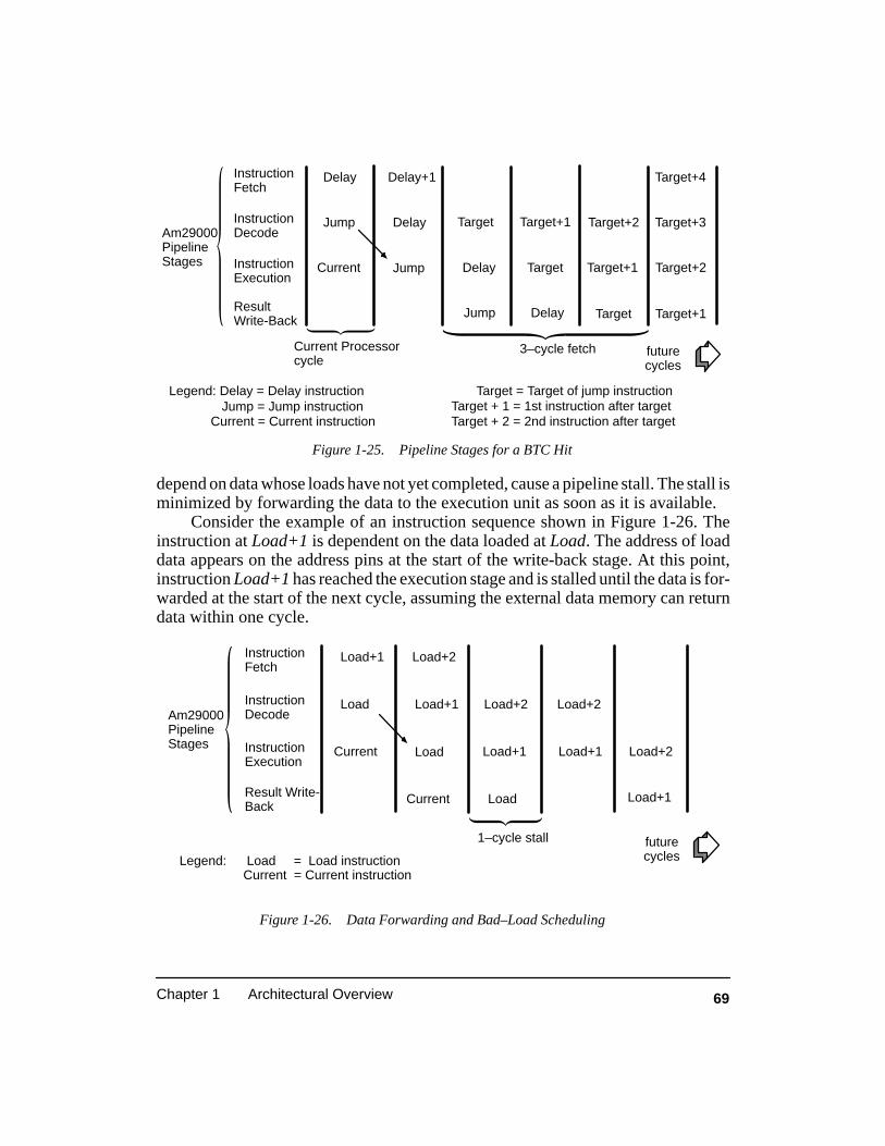
69Chapter 1 Architectural Overview
Target
Current Processorcycle
InstructionFetch
InstructionDecode
InstructionExecution
ResultWrite-Back
Am29000PipelineStages
Delay
Jump
Current
Delay
Delay
Delay
Jump
Jump
Target+2
Target+2
Target+4
Target+3
Delay+1
Target+1
Target Target+1
Target Target+1
3–cycle fetch
Figure 1-25. Pipeline Stages for a BTC Hit
Target = Target of jump instructionLegend: Delay = Delay instructionJump = Jump instruction
Current = Current instructionTarget + 1 = 1st instruction after targetTarget + 2 = 2nd instruction after target
futurecycles
depend on data whose loads have not yet completed, cause a pipeline stall. The stall isminimized by forwarding the data to the execution unit as soon as it is available.
Consider the example of an instruction sequence shown in Figure 1-26. Theinstruction at Load+1 is dependent on the data loaded at Load. The address of loaddata appears on the address pins at the start of the write-back stage. At this point,instruction Load+1 has reached the execution stage and is stalled until the data is for-warded at the start of the next cycle, assuming the external data memory can returndata within one cycle.
InstructionFetch
InstructionDecode
InstructionExecution
Result Write-Back
Am29000PipelineStages
Legend: Load = Load instruction Current = Current instruction
Load+1
Load
Current
Load+1
Load+1Load
LoadCurrent
Load+2
Load+2 Load+2
Load+1 Load+2
Load+1
1–cycle stall
Figure 1-26. Data Forwarding and Bad–Load Scheduling
futurecycles
70 Evaluating and Programming the 29K RISC Family
If the instruction were not dependent on the result of the load, it would haveexecuted without delay. Because of data forwarding and a 1-cycle data memory, theload data would be available for instruction Load+2 without causing a pipeline stall.
1.14 ARCHITECTURAL SIMULATION, sim29
AMD has for a long time made available a 29K simulator which accuratelymodels the processor operation. This simulator, known as the Architectural Simula-tor, can be configured to incorporate memory system characteristics. Since memorysystem performance can greatly influence overall system performance, the use of thesimulator before making design decisions is highly recommended.
Simulation of all the 29K family members is supported, making the simulatoruseful in determining processor choice [AMD 1991c][AMD 1993c]. For example,does a floating–point intensive application require an Am29050 or will an Am29000suffice? Alternatively, the performance penalties of connecting the data and instruc-tion busses together on a 3–bus Harvard Architecture processor can be determined.
Because the simulator models detailed processor operation, such as pipelinestages, cache memory, instruction prefetch, channel operation and much more, thesimulation run–times are longer than if the Instruction Set Simulator (ISS) were used.Consequently, the Architectural Simulator is seldom used for program debugging.The ISS simulator is described in Chapter 7 (Software Debugging). This is one of thereasons that the Architectural simulator does not utilize the Universal Debugger In-terface (see section 7.5). Without a UDI interface, the simulator can not support inter-active debugging. Simulation results are directed to a log file. Interpretating theirmeaning and dealing with log file format takes a little practice; more on this later.
When used with a HIF conforming operating system, the standard input and out-put for the simulated program use the standard input and output for the executablesimulator. Additionally, the 29K program standard output is also written to the simu-lation log file. AMD does not supply the simulator in source form; it is available inbinary for UNIX type hosts and 386 based PCs. The simulator driver, sim29, sup-ports several command line options, as shown below. AMD updated the simulatorafter version 1.1–8; the new version is compatible with the old and simulates at morethan four times the speed. The old simulator is still used with the Am29000 andAm29050 processors. Only the new simulator models the Am2924x microcontrol-lers and newer 2–bus processors. The following description of command line optionscovers both simulator versions.
sim29 [–29000 | –29005 | –29030 | –29035 | –29050 ... –29240][–cfg=xx] [–d] [–e eventfile] [–f freq] [–h heapsize] [–L] [–n][–o outputfile] [–p from–to] [–r osboot] [–t max_sys_calls][–u] [–v] [–x[codes]] [–dcacheoff] [–icacheoff] [–dynmem <val>]execfile [... optional args for executable]
71Chapter 1 Architectural Overview
OPTIONS
–29000|29005|29030|29035|29040|29050|29200|29205|29240|...
Select 29K processor, default is Am29000. Depending on the proces-sor selected, the old or new simulator is selected.
–cfg=xx Normally the simulator starts execution at address 0, with the proces-sor Configuration Register (CFG) set to the hardware default value.Its the application code or the osboot code responsibility to modifythe CFG registers as necessary. Alternatively, the CFG register can beinitialized from the command line. The –cfg option specifies the set-ting for CFG, where xx is a 1 to 5 digit HEX number. If the –cfg optionis used, no run–time change to CFG will take effect, unless anAm292xx processor is in use. The –cfg option is seldom used; itshould be used where an osboot file is not supplied with the –r option.Alternatively it can be used to override the cache enable/disable op-eration of osboot code. This can enable the effects of cache to be de-termined without the need to built a new osboot file. The –cfg optionis not supported by the newer simulator. Caches can be disabled usingthe new –icacheoff and –dcacheoff options.
–d This option instructs the simulator to report the contents of processorregisters in the logfile at end of simulation.
–dcacheoff This option is only available with the newer simulator. When used itcauses the Configuration Register (CFG) to be set for data cache dis-able.
–dynmem <val>
During execution a program may access a memory region out withany loaded memory segment or heap and stack region. The simulatorcan be instructed to automatically allocate (val=1) memory for the ac-cessed region. Alternatively (default, val=0) an access violation is re-ported.
–e eventfile An event file is almost always used. It enables memory system char-acteristics to be defined and the simulation to be controlled (see sec-tion 1.14.1).
–f frequency Specify CPU frequency in MHz; the default for the Am292xx andAm29035 is 16 MHz; the Am2900x default is 25 MHz; and the de-fault frequency for the Am29030 and Am29050 is 40 MHz.
–h heapsize This option specifies the amount of resource memory available to thesimulated 29K system. This memory is used for the register stack andmemory stack support as well as the run–time heap. The default sizeis 32 K bytes; a heapsize value of 32.

72 Evaluating and Programming the 29K RISC Family
–icacheoff This option is only available with the newer simulator. When used itcauses the Configuration Register (CFG) to be set for instructioncache disable.
–L This option is similar in nature to the –cfg option. It can be used to se-lect the large memory model for the Am292xx memory banks. Nor-mally this selection is performed in the osboot file. However, the –Loption can be used to override the osboot settings, without having tobuild a new osboot file. This option is currently not supported in thenewer simulator.
–n Normally the simulator will allow access to the two words followingthe end of a data section, without generating an access violation.Some of the support library routines, such as strcpy(), used by 29Kapplication code, use a read–ahead technique to improve perfor-mance. If the read–ahead option is not supported, then the –n optionshould be used. Only the older simulator supports this option. Thenewer simulator always allows access to the words just past the end ofthe data section.
–o outputfile The simulator normally presents simulation results in file sim.out.However an alternative result file can be selected with this option.
–p from–to The simulator normally produces results of a general nature, such asaverage number of instructions per second. It is possible, using thisoption to examine the operation of specific code sequences within ad-dress range from to to.
–r osboot The simulator can load two 29K executable programs via command–line direction: osboot and program. It is normal to load an operatingsystem to deal with application support services; this is accomplishedwith osboot. It is sometimes referred to as the romfile, because whenused with 29K family members which support separate ROM andInstruction spaces, osboot is loaded into ROM space. AMD suppliesa HIF conforming operating system called OS–boot which is general-ly used with the –r option. Your simulation tool installation shouldhave a 29K executable file called osboot, romboot or even pumabootwhich contains the OS–boot code. Care should be taken to identifyand use the correct file. The newer simulator will automatically selecta default osboot file from the library directory if the –r option is notused.
–t max_sys_calls
Specify maximum number of system call types that will be used dur-ing simulation This switch controls the internal management of the
73Chapter 1 Architectural Overview
simulator; it is seldom used and has a default value of 256. This optionis not supported by the newer simulator.
–u The Am292xx microcontroller family members have built–in ROMand DRAM memory controllers. Programmable registers are used toconfigure the ROM and DRAM region controllers. If the –u option isused, application code in file program can modify the controller set-tings, otherwise only code in osboot can effect changes. This protectsapplication code from accidentally changing the memory region con-figuration.
–v The OS–boot operating system, normally used to implement the os-boot file, can modify its warm–start operation depending on the valuein register gr104 (see section 7.4). The –v switch causes gr104 to beinitialized to 0. When OS–boot is configured to operate with or with-out MMU support, a run–time gr104 value of 0 will turn off MMUuse.
–x[code] If a 29K error condition occurs during simulation, execution is notstopped. The –x option can be used to cause execution to stop under aselected range of error conditions. Note, the option is not supportedby the newer simulator. Each error condition is given a code letter. If –x is used with no selected codes, then all the available codes are as-sumed active. Supported code are:A Address error; data or instruction address out of bounds.K Kernel error; illegal operation in Supervisor mode.O Illegal opcode encountered.F Floating–point exception occurred; such as divide by zero.P A protection violation occurred in User modeS An event file error detected.
execfile Name of the executable program to be loaded into memory; followedby any command–line arguments for the 29K executable. It is impor-tant that the program be correctly linked for the intended memory sys-tem. This is particularly true for systems based on Am292xx proces-sors. They have ROM and DRAM regions which can have very dif-ferent memory access performance. If SRAM devices are to be usedin the ROM region, it is important that the application be linked forthe ROM region use rather than the DRAM.
It is best to run sim29 with the –r osboot option (this is the default operation withthe newer simulator). This is sometimes called cold–start operation. The osboot pro-gram must perform processor initialization, bringing the processor into what isknown as the warm–start condition. At this point, execution of the loaded programcommences. It is possible to run the older simulator without the use of an osboot file;

74 Evaluating and Programming the 29K RISC Family
this is known as warm–start simulation. When this is done the simulator initializesthe processor special registers CFG and CPS to a predefined warm–start condition.AMD documentation explains the chosen settings; they are different for each proces-sor. Basically, the processor is prepared to run in User mode with traps and interruptsenabled and cache in use.
To support osboot operation, the simulator prepares processor registers beforeosboot operation starts (see Figure 1-27).
register stack size
memory stack size
first instruction of User loaded code
end address of program data
start address of program data
end address of program text
start address of program text
address of end of physical memory
Operating system control info.
start of command line args (argv)
Figure 1-27. Register Initialization Performed by sim29
gr96
gr97
gr98
gr99
gr100
g101
gr102
gr103
gr104
gr105
argument pointer, argv
argument count, argclr2
lr3
The initial register information is extracted from the program file. Via the regis-ter data, the osboot code obtains the start address of the program code. If osboot codeis not used (no –r command–line switch when using the older simulator), the 29KProgram Counter is initialized to the start address of program code, rather than ad-dress 0. To support direct entry into warm–start code, the program argument in-formation is duplicated in lr2 and lr3. Normally this information is obtained by os-boot using the data structure pointed to by gr103.
The simulator intercepts a number of HIF service calls (see section 2.2). Theseservices mainly relate to operating system functions which are not simulated, butdealt with directly by the simulator. All HIF services with identification numbers be-low 256 are intercepted. Additionally service 305, for querying the CPU frequency,is intercepted. Operating services which are not intercepted, must be dealt with by theosboot code. The simulator will intercept a number of traps if the –x[codes] com-mand line option is used; otherwise all traps are directed to osboot support code, orany other trapware installed during 29K run–time.

75Chapter 1 Architectural Overview
1.14.1 The Simulation Event File
Simulation is driven by modeling the 29K processor pipeline operation. Instruc-tions are fetched from memory, and make their way through the decode, execute andwrite–back stages of the four–stage pipeline. Accurate modeling of processor inter-nals enables the simulator to faithfully represent the operation of real hardware.
The simulator can also be driven from an event file. This file contains com-mands which are to be performed at specified time values. All times are given in pro-cessor cycles, with simulation starting at cycle 0. The simulator examines the eventfile and performs the requested command at the indicated cycle time.
The syntax of the command file is very simple; each command is entered on asingle line preceded with a integer cycle–time value. There are about 15 to 20 differ-ent commands; most of them enable extra information to be placed in the simulationresults file. Information such as recording register value changes, displaying cachememory contents, monitoring floating–point unit operation, and much more. A se-cond group of commands are mainly used with microcontroller 29K family mem-bers. They enable the on–chip peripheral devices to be incorporated in the simula-tion. For example, the Am29200 parallel port can receive and transmit data from filesrepresenting off–chip hardware.
In practice, most of these commands are little used; with one exception, the SETcommand (see note below). Most users of sim29 simply wish to determine how acode sequence, representative of their application code, will perform on different29K family members with varying memory system configurations. The SET com-mand is used to configure simulation parameters and define the characteristics ofsystem memory and buss arrangements. I will only describe the parameters used withthe MEM option to the SET command.The cycle–time value used with the com-mands of interest is zero, as the memory system characteristics are established beforesimulation commences. One other option to the SET command of interest isSHARED_ID_BUS; when used, it indicates the Instruction and Data buses are con-nected together. This option only makes sense with 3–bus members of the 29K fami-ly. All the 2–bus members already share a single bus for data and instructions, thesecond bus being used for address values. The syntax for the commands of interest isshow below:
0 SET_SHARED_ID_BUS0 SET MEM access TO value
Note, the SET command is accepted by both the older and newer versions of thesimulator. However, the newer version has an abbreviation to the SET commandshown below; the “SET MEM” syntax is replaced by a direct command and there isno need for the “TO”.

76 Evaluating and Programming the 29K RISC Family
0 SET MEM IWIDTH TO 32 older syntax0 ROMWIDTH 32 newer syntaxromwidth 32 newer syntax
Am29000 and Am29050
Note, when the Instruction bus and Data busses are tied together with 3–bus pro-cessors, the ROM space is still decoded separately from the Instruction space. Tyingthe busses together will reduce system performance, because instructions can nolonger be fetched from Instruction space, or ROM space, while the Data bus is beingused.
Considering only the most popular event file commands simplifies the presenta-tion of sim29 operation; and encourages its use. Those wishing to know more aboutevent file command options should contact AMD. They readily distribute the sim29executable software for popular platforms and with relevant documentation.
Table 1-5 shows the allowed access and value parameters for 3–bus members ofthe 29K family, that is, the Am29000 and Am29050 processors. Off–chip memorycan exist in three separately addressed spaces: Instruction, ROM , and Data. Memoryaddress–decode and access times (in cycles) must be entered for each address spacewhich will be accessed by the processor; default values are provided.
Table 1-5. 3–bus Processor Memory Modeling Parameters for sim29Instruction ROM Data Value Default Operation
IDECODE RDECODE DDECODE 0–n 0 Decode addressIACCESS RACCESS DRCCESS 1–n 1 First read
DWACCESS 1–n 1 First writeIBURST RBURST DBURST T|F false Burst–mode supportedIBACCESS RBACCESS DBRACCESS 1–n 1 Burst read
DBWACCESS 1–n 1 Burst write
If a memory system supports burst mode, the appropriate *BURST access pa-rameter must be set to value TRUE. The example below sets Instruction memory ac-cesses to two cycles; subsequent burst mode accesses are single–cycle. The examplecommands only affect Instruction memory; additional commands are required to es-tablish Data memory access characteristics. Many users of the simulator only requirememory modeling parameters from Table 1-5, even if DRAM is in use.
0 SET MEM IACCESS TO 20 SET MEM IBURST TO true0 SET MEM IBACCESS TO 1
If DRAM memory devices are used, there are several additional access parame-ters which can be used to support memory system modeling (see Table 1-6). DRAM

77Chapter 1 Architectural Overview
devices are indicated by the *PAGEMODE parameter being set. The 29K family in-ternally operates with a page size of 256 words, external DRAM memory always op-erates with integer multiples of this value. For this reason, there is never any need tochange the *PGSIZE parameter setting from its default value. The first read access toDRAM memory takes *PFACCESS cycles; second and subsequent read accessestake *PSACCESS cycles. However, if the memory system supports burst mode, sub-sequent read accesses take *PBACCESS cycles rather than *PSACCESS.
If static column DRAM memories are used, then memory devices do not requireCAS signals between same–page accesses. Static column memory use is indicated bythe *STATCOL parameter. Initial page accesses suffer the additional *PRECHAR-GE access penalties, subsequent accesses all have same access latencies. Note, burstmode access can also apply to static column DRAM memory. Table 1-7 showsmemory modeling parameters for static column memories.
Table 1-6. 3–bus Processor DRAM Modeling Parameters for sim29 (continued)
Instruction ROM Data Value Default Operation
IPAGEMODE PAGEMODE DPAGEMODE T|F false Memory is pagedIPGSIZE RPGSIZE DPGSIZE 1–n 256 Page size in wordsIPFACCESS RPFACCESS DPFRACCESS 1–n 1 First read in page mode
DPFWACCESS 1–n 1 First write in page modeIPSACCESS RPSACCESS DPSRACCESS 1–n 1 Secondary read within page
DPSWACCESS 1–n 1 Secondary write within pageIPBACCESS RPBACCESS DPBRACCESS 1–n 1 Burst read within page
DPBWACCESS 1–n 1 Burst write within page
Table 1-7. 3–bus Processor Static Column Modeling Parameters for sim29 (continued)
Instruction ROM Data Value Default Operation
ISTATCOL RSTATCOL DSTATCOL T|F false Static column memory usedISMASK RSMASK DSMASK 0xffffff0 0 Column address mask, 64–wordsIPRECHARGE RPRECH DPRECHARGE 0–n 0 Precharge on page crossingISACCESS RSACCESS DSRACCESS 1–n 1 Read access within static column
DSWACCESS 1–n 1 Write access within static column
Separate regions of an address space may contain more than one type ofmemory device and control mechanism. To support this, memory banking is pro-vided for in the simulator (see Table 1-8). The [I|R|D]BANKSTART parameter isused to specify the start address of a memory bank; a bank is a contiguous region ofmemory of selectable size, within an indicated address space. Once the *BANK-

78 Evaluating and Programming the 29K RISC Family
START command has been used, all following commands relate to the current bank,until a new bank is selected. This type of command is more frequently used with mi-crocontroller members of the 29K family.
Table 1-8. 3–bus Processor Memory Modeling Parameters for sim29 (continued)
Instruction ROM Data Value Default Operation
IBANKSTART RBANK DBANKSTART 0–n – Start address of memory regionIBANKSIZE BBAKSIZE DBANKSIZE 1–n 1 Size in bytes of memory region
Am29030 and Am29035The parameters used with the SET command, when simulating 2–bus 29K fami-
ly members are a little different from 3–bus parameters (see Table 1-9). The parame-ters shown are for the older simulator, but they are accepted by the new simulator. Fora list of alternative parameters, which are only accepted by the newer simulator, seethe following Am29040 section. There is no longer a ROM space, and althoughinstructions and data can be mixed in the same memory devices, separate modelingparameters are provided for instruction and data accesses.
Table 1-9. 2–bus Processor Memory Modeling Parameters for older sim29
Instruction Data Value Default Operation
IACCESS DRACCESS 2–n 2 First read from SRAMDWACCESS 2–n 2 First write from SRAM
IBURST DBURST T|F true Burst–mode supported IBACCESS DBRACCESS 1–n 1 Burst read within page
DBWACCESS 1–n 1 Burst write within pageIWIDTH DWIDTH 8,16,32 32 Memory widthIPRECHARGE DPRECHARGE 0–n 0 Precharge on page crossingIPACCESS DPRACCESS 2–n 2 First access in page mode
DPWACCESS 2–n 2 First write in page modeIBANKSTART DBANKSTART 0–n – Start address of memory regionIBANKSIZE DBANKSIZE 1–n 1 Size in bytes of memory regionHALFSPEED HALFSPEED T|F false Memory system is 1/2 CPU speed
Consider accessing memory for instructions; IACCESS gives the access time,unless DRAM is used, in such case, access time is given by IPACCESS. The use ofDRAM is indicated by the *PRECHARGE parameter value being non zero. First ac-cesses to DRAM pages suffer an addition access delay of *PRECHARGE. If burstmode is supported, with all memory device types, the access times for instructionmemory, other than the first access, is given by IBACCESS.

79Chapter 1 Architectural Overview
Both the current 2–bus 29K family members support Scalable Clocking, enab-ling a half speed external memory system. They also support narrow, 8–bit or 16–bit,memory reads. The Am29035 processor also supports dynamic bus sizing. All exter-nal memory accesses can be 16–bit or 32–bit; processor hardware takes care of multi-ple memory accesses when operating on 32–bit data. As with the 3–bus 29K familymembers, the simulator provides for memory banking. This enables differentmemory devices to be modeled within specified address ranges.
Alternative Am29030, Am29035 and Am29040As stated in the previous section, the newer sim29 can accept the memory mod-
eling parameters used by the older sim29. However, the newer simulator can operatewith alternative modelling commands; these are shown on Table 1-10. Commandscan be in upper or lower case, but they are shown here in lower case. A list of avail-able simulator commands can be had by issuing the command “sim29 –29040–help”. An example of Am29040 processor simulation can be found in section 8.1.3
Table 1-10. 2–bus Processor Memory Modeling Parameters for newer sim29
Command value Operation
rombank <adds> <size> Size and address of ROM/SRAMrambank <adds> <size> Size and address of DRAMhalfspeedbus true|false Scalable Clocking (default=false)logging true|false Loging to file sip.log (default=false)
ROM/SRAM DRAM Value Default Operation
romread ramread 2–n 2 First readromwrite ramwrite 2–n 2 First writeromburst ramburst T|F true Enable burst mode addressingrombread rambread 1–n 1 Burst read within pagerombwrite rambwrite 1–n 1 Burst write within pagerompage rampage T|F true Enable page moderompread rampread 2–n 2 Single read within pagerompwrite rampwrite 2–n 2 Single write within pagerompwidth ramwidth 16,32 32 Bit width of memory
ramprecharge 0–n 0 DRAM precharge timerampprecharge 0–n 0 Page mode DRAM prechageramrefrate 0–n 0 DRAM refresh rate (0=off)
ROM and SRAM memory types are modeled with the same set of commands.The simulator allocates a default ROM/SRAM memory bank starting at address 0x0.Unless a RAMBANK command is used to allocate a DRAM memory section at a lowmemory address, all code and data linked for low memory addresses will be allocatedto the default ROM/SRAM memory bank.

80 Evaluating and Programming the 29K RISC Family
DRAM memory is modelled with the RAM* modelling commands. A defaultDRAM memory section is established at address 0x4000,0000. Unless aROMBANK command is used to allocate a ROM/SRAM memory bank at thisaddress range, all accesses to high memory will be satisfied by the default DRAMmemory.
The default linker command files used with the High C 29K tool chain, typicallylinks programs for execution according the the above default memory regions. How-ever, older release of the compiler tool chain (or other tool chains) may link for differ-ent memory models. This would require the use of RAMBANK–type commands toestablish the correct memory model. Alternatively, a compiler command file couldbe used to ensure a program is linked for the default simulator memory mode (seesection 2.3.6).
Am29200 and Am29205The simulator does not maintain different memory access parameters for
instruction and data access when modeling microcontroller members of the 29Kfamily. However, it does support separate memory modeling parameters for DRAMand ROM address regions (see Table 1-11). Each of these two memory regions has itsown memory controller supporting up to four banks. A bank is a contiguous range ofmemory within the address range accessed via the region controller. The DRAM re-gion controller is a little more complicated than the ROM region controller. The pa-rameters shown in Table 1-11 are for the older simulator, but they are accepted by thenew simulator. For a list of alternative parameters, which are only accepted by thenewer simulator, see the following Am29240 section.
The DRAM access is fixed at four cycles (1 for precharge + 3 for latency), it cannot be programmed. Subsequent accesses to the same page take four cycles unlesspagemode memories are supported. Note the first access is only three cycles ratherthan four, as the RAS will already have met the precharge time. Basically, to prechar-ge the RAS bit lines, all RAS lines need to be taken high in between each change of therow addresses. A separate cycle is needed for precharge when back–to–back DRAMaccesses occurs. Use of pagemode memories is indicated by the PAGEMODE pa-rameter being set; when used, the processor need not supply RAS memory strobe sig-nals before page CAS strobes for same page accesses. This reduces subsequent pageaccess latency to three cycles. Additionally, when pagemode is used and a data burstis attempted within a page, access latency is two cycles. The DRAM memory widthcan be set to 16 or 32–bits. Of course when an Am29205 is used, all data memoryaccesses are restricted by the 16–bit width of the processor data bus.
To explain further, access times to DRAM for none pagemode memories followthe sequence:
X,3,4,4,4,X,3,4,4,4,X,X,3,X,3,...

81Chapter 1 Architectural Overview
Where X is a non–DRAM access, say to ROM or PIA space. For DRAM sys-tems supporting pagemode the sequence would be:
X,3,2,2,2,<boundary crossing>,4,2,2,<boundary crossing>,X,3,2,2,2
Memory devices located in ROM space can be modeled with a wider range ofparameter values. Both SRAM and ROM devices can be modeled in ROM space. Us-ing the RBANKNUM parameter, the characteristics of each bank can be selectivelydescribed. Burst–mode addressing is only supported for instruction or data reading.When the burst option is used (RBURST set to TRUE), read accesses, other than thefirst for a new burst, take RBACCESS cycles rather than the standard RRACCESScycles. Memory device widths can be 8, 16 or 32–bits. If an Am29205 microcontrol-ler is being modeled, memory accesses wider than the 16–bit bus width always re-quire the processor to perform multiple memory transfers to access the requiredmemory location.
Table 1-11. Microcontroller Memory Modeling Parameters for sim29
ROM/SRAM value default DRAM Value Default (Am29200) Operation
1 Precharge on page crossingRRACCESS 1–n 1 3 First readRWACCESS 2–n 2 3 First writeRBURST T|F false Burst address in ROM regionRBACCESS 1–n 1 2 Burst read within page
2 Burst write within pageROMWIDTH 8,16,32 32 DRAMWIDTH 16,32 32 Width of memory
PAGEMODE T|F false Page mode supportedRBANKNUM 0–3 – DBANKNUM 0–3 – Select which memory bank
Preparing sim29 for modeling an Am29200 system is not difficult. The follow-ing commands configure the first two ROM banks to access non–burst–mode memo-ries which are 32–bits wide, and have a 1–cycle read access, and a 2–cycle write ac-cess.

82 Evaluating and Programming the 29K RISC Family
0 COM ROM bank 0 parameters0 SET MEM rbanknum to 00 SET MEM rraccess to 10 SET MEM rwaccess to 2
0 COM ROM bank 1 parameters0 SET MEM rbanknum to 10 SET MEM rraccess to 10 SET MEM rwaccess to 2
The following DRAM parameters, like the ROM parameters above, are correctfor modeling an SA29200 evaluation board. The first DRAM bank is configured tosupport pagemode DRAM access, giving access latencies of 4:3:2 (4 for first, 3 forsame–page subsequent, unless they are bursts which suffer only 2–cycle latency).
0 COM DRAM bank 0 parameters0 SET MEM dbanknum to 00 SET MEM dpagemode to true
Alternative Am2920x and Am2924x
As stated in the previous section, the newer sim29 can accept the memory mod-eling parameters used by the older sim29. However, the newer simulator can operatewith alternative modelling commands; these are shown on Table 1-12. Commandscan be in upper or lower case, but they are shown here in lower case. A list of avail-able simulator commands can be had by executing the command “sim29 –29240–help”. An example of Am29200 microcontroller simulation can be found in section8.1.

83Chapter 1 Architectural Overview
Table 1-12. Microcontroller Processor Memory Modeling Parameters for newer sim29
Command value default Operation
rombank <adds> <size> Size and address of ROM/SRAMrambank <adds> <size> Size and address of DRAMhalfspeedbus true|false Scalable Clocking (default=false)logging true|false Loging to file sip.log (default=false)parallelin <file> [<speed>] Parallel port input fileparallelout <file> [<speed>] Parallel port output fileserialin a|b <file> [ [<baud>] Serial port, a or b, input fileserialout a|b <file> [<baud>] Serial port, a or b, output file
ROM/SRAM DRAM Value Default (Am29240) Operation
romread 1–n 1 First readromwrite 2–n 2 First writeromburst T|F false Enable burst mode addressingrombread 1–n 1 Burst read within page
rampage T|F true Enable page moderompwidth ramwidth 8,16,32 32 Bit width of memory
ramrefrate 0–n 255 DRAM refresh rate (0=off)
ROM and SRAM memory types are modeled with the same set of commands.The simulator automaticlay allocates ROM/SRAM memory bank 0. Using theROMBANK parameter, the characteristics of each bank can be selectively de-scribed. The default parameters are typically for a relatively fast memory system
The DRAM memory access times are fixed by the processor specification.However, there are some DRAM modelling commands enabling selection ofmemory system with and pagemode devices. The simulator automatically allocatesDRAM memory bank 0 at address 0x4000,0000. All accesses to memory above thisaddress will be satisfied by the DRAM memory bank.
It is usually less of a problem linking programs for execution on a 29K micro-controller; as the processor hardware dictates, to some extend, the allowed memoryregions. The default linker command files used with the High C 29K tool chain, typi-cally link programs for execution according the the processor specificity memory re-gions. Compiler command files are described in section 2.3.6.
1.14.2 Analyzing the Simulation Log File
Running the architectural simulator is simple but rather slow. The inclusion ofdetail about the processor pipeline results in slow simulation speeds. For this reason,users typically select a portion of their application code for simulation. This portionis either representative of the overall code or subsections whose operation is criticalto overall system performance.

84 Evaluating and Programming the 29K RISC Family
Older sim29 Log File Format
For demonstration purposes I have merely simulated the “hello world” programrunning on an Am29000 processor. The C source file was compiled with the High C29K compiler using the default compiler options; object file hello was produced bythe compile/link process. The memory model was the simulator default, single–cycleoperation. Given the selection of default memory parameter, there is no need for aneventfile establishing memory parameters. However, I did use an eventfile with thefollowing contents:
0 log on channel
This option has not previously been described; it enables the simulator to pro-duce an additional log file of channel activity. This can occasionally be useful whenstudying memory system operation in detail. The simulator was started with the com-mand:
sim29 –29000 –r /gnu/29k/src/osboot/sim/osboot –e eventfile hello
Two simulation result files were produced; the most important of which, the de-fault simulation output file, sim.out, we shall briefly examine. The channel.out filereports all instruction and data memory access activity. The contents of the sim.outfile are shown below exactly as produced by the simulator:
AMD ARCHITECTURAL SIMULATOR, V# 1.0–17PC ### T=3267 Am29000 Simulation of ”hello” complete –– successful––––––––––––––––––––––––––––––––––––––––––––––––––––– <<<<< S U M M A R Y S T A T I S T I C S >>>>>
CPU Frequency = 25.00MHz
Nops:50 total instructions = 2992
User Mode: 291 cycles (0.00001164 seconds)Supervisor Mode: 2977 cycles (0.00011908 seconds)Total: 3268 cycles (0.00013072 seconds)
Simulation speed: 22.89 MIPS (1.09 cycles per instruction)
–––––––––– Pipeline –––––––––– 8.45% idle pipeline:
6.46% Instruction Fetch Wait 0.46% Data Transaction Wait 0.18% Page Boundary Crossing Fetch Wait 0.00% Unfilled BTCache Fetch Wait 0.49% Load/Store Multiple Executing 0.03% Load/Load Transaction Wait
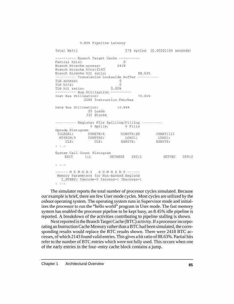
85Chapter 1 Architectural Overview
0.83% Pipeline Latency
Total Wait: 276 cycles (0.00001104 seconds)
–––––––––– Branch Target Cache ––––––––––Partial hits: 0Branch btcache access: 2418Branch btcache hits:2143Branch btcache hit ratio: 88.63%–––––––––– Translation Lookaside Buffer ––––––––––TLB access: 0TLB hits: 0TLB hit ratio: 0.00%–––––––––– Bus Utilization ––––––––––Inst Bus Utilization: 70.01%
2288 Instruction Fetches
Data Bus Utilization: 10.86% 20 Loads 335 Stores
–––––––––– Register File Spilling/Filling –––––––––– 0 Spills, 0 Fills
Opcode Histogram ILLEGAL: CONSTN:6 CONSTH:68 CONST:121 MTSRIM:5 CONSTHZ: LOADL: LOADL: CLZ: CLZ: EXBYTE: EXBYTE: . . .
System Call Count Histogram EXIT 1:1 GETARGS 260:1 SETVEC 289:2 . . .
–––––– M E M O R Y S U M M A R Y –––––– Memory Parameters for Non–banked Regions I_SPEED: Idecode=0 Iaccess=1 Ibaccess=1. . .
The simulator reports the total number of processor cycles simulated. Becauseour example is brief, there are few User mode cycles. Most cycles are utilized by theosboot operating system. The operating system runs in Supervisor mode and initial-izes the processor to run the “hello world” program in User mode. The fast memorysystem has enabled the processor pipeline to be kept busy, an 8.45% idle pipeline isreported. A breakdown of the activities contributing to pipeline stalling is shown.
Next reported is the Branch Target Cache (BTC) activity. If a processor incorpo-rating an Instruction Cache Memory rather than a BTC had been simulated, the corre-sponding results would replace the BTC results shown. There were 2418 BTC ac-cesses, of which 2143 found valid entries. This gives a hit ratio of 88.63%. Partial hitsrefer to the number of BTC entries which were not fully used. This occurs when oneof the early entries in the four–entry cache block contains a jump.

86 Evaluating and Programming the 29K RISC Family
If the operating system had arranged for Translation Look–Aside Buffer (TLB)use then the next section reports its activity. In the example, the application ran withphysical addressing which does not require TLB support. Next reported is bus activ-ity. The large number of processor registers results in little off–chip data memory ac-cess, and hence Data Bus utilization. The Instruction Bus is used to fill the Instruc-tion Prefetch Buffer and BTC, and shows much higher utilization. Typically, pro-grams are more sensitive to instruction memory performance than data memory.
The simulator then produces a histogram of instruction and system call usage.The listing above only shows an extract of this information, as it is rather large. Ex-amining this data can reveal useful information, such as extensive floating–pointinstruction use.
Finally reported is a summary of the memory modeling parameters used duringsimulation. This information should match with the default parameters or any param-eters established by the eventfile. It is useful to have this information recorded alongwith the simulation results.
Newer sim29 Log FIle Format As with the previous demonstration, the “hello world” program is used here to
show the output format of the newer architectural simulator. The selected processoris this time an Am29240 microcontroller. The C source file was compiled with theHigh C 29K compiler using the –O4 compiler options; object file hello was producedby the compile/link process. The memory model was the simulator default. Given theselection of default memory parameter, there is no need for an eventfile to establishmemory parameters. The simulator was started with the command shown below.Note, there is no need to use the –r option and specify an osboot file.
sim29 –29240 hello
The simulation result file, sim.out, was produced. The contents of the sim.outfile are shown below exactly as produced by the simulator:
Am292xx Architectural Simulator, Version# 2.4 Command line: /usr/29k/bin/sim240 –29240 hello
Boot file: /usr/29k/lib/osb24xText section: 00000000 – 0000001fText section: 00000020 – 00000333Text section: 00000340 – 0000035fText section: 00000360 – 00006b6bBSS section: 40000400 – 400007df
Application file: helloText section: 40010000 – 4001332bText section: 4001332c – 4001333bText section: 4001333c – 4001334bData section: 40014000 – 40014993

87Chapter 1 Architectural Overview
Lit section: 40014994 – 40014c63BSS section: 40014c64 – 40014ca3
Argv memory: 400150a0 – 4001589fHeap memory: 40015ca0 – 40035c9fMemory stack: 40fbf7f0 – 40fdffefRegister stack: 40fdfff0 – 410007efVector Area: 40000000 – 400003ff
ROM: Address Size Rd Wr Bmd BRd Wid 0x0 * 1 1 0 1 32RAM: Address Size Rd Wr Pmd PRd PWr Wid Ref 0x40000000 * 2 2 1 1 1 32 255
Half speed memory = 0Starting simulation...
hello world
HIF Exit: Value = 12Simulation summary:
Cycles: 7101 Supervisor mode = 100.0% User mode = 0.0%
MIPS = 18.8 (25.0 Mhz * ((5342 instructions)/(7101 cycles)))
Pipeline: Average run length= 5.9 instructions between jumps taken Fetches not used due to jumps = 299
PipeHold: 1759 cycles = 24.8% Fetch waits: 1520 cycles = 21.4% Load waits: 133 cycles = 1.9% Store waits: 79 cycles = 1.1% Load Multiple waits: 3 cycles = 0.0% Store Multiple waits: 24 cycles = 0.3%
Channel: Rom: accesses = 809 Rom: average cycles per access = 1.0 Ram: accesses = 1959 Ram: average cycles per access = 1.7 Ram: average cycles waiting for precharge = 0.2 Ram: average cycles waiting for refresh = 0.2
Instruction Cache Size = 4 Kbytes Hit ratio = 66.4% (3766/5673)
Data Cache Size = 2 Kbytes Hit ratio = 63.6% (136/214)
The format of Log File will appear familiar to those experienced with the olderarchitectural simulator; the total number of processor cycles simulated is reported.There are no User mode cycles as the default osboot (osb24x ) executed the hello

88 Evaluating and Programming the 29K RISC Family
program in Supervisor mode. Most cycles are utilized by the osboot operating sys-tem. The relatively fast memory system has enabled the processor pipeline to be keptbusy, a 24.8% idle pipeline is reported. A breakdown of the activities contributing topipeline stalling is shown. Most pipeline stalls are due to instruction fetching; theDRAM memory has a 2–cycle first access time, rather than the ideal 1–cycle. Thenewer simulator reports the average number of instructions executed between jumpor branch instructions. The run length is shown to be 5.9 instructions, which is typicalof a 29K program.
Next reported is Channel activity. All load and store instructions make use of theChannel. Statistics are presented separately for the ROM/SRAM and DRAMmemory systems. Typically, performance is much more sensitive to instructionmemory access rather than accesses to data. This is particularly true with the 29Kfamily due to its large number of on–chip registers.
Next reported is on–chip cache activity. There were 5673 accesses to theinstruction cache, of which 66.4% found valid entries. The Am29240 has the benefitof a data cache and the results are shown. The hello program is small and only 214data cache accesses were made, of which 63.4% hit in the cache.
Reported in the sim.out file before simulation started are the memory modelingparameters used during simulation. This information should match with the defaultparameters or any parameters established by the eventfile. It is useful to have this in-formation recorded along with the simulation results. The values reported are shownagain below:
ROM: Address Size Rd Wr Bmd BRd Wid 0x0 * 1 2 0 1 32RAM: Address Size Rd Wr Pmd PRd PWr Wid Ref 0x40000000 * 2 2 1 1 1 32 255
Half speed memory = 0
The ROM section refers to both ROM and SRAM memory. The tokens used area little cryptic. For example, “Rd” refers to memory read cycles. And “BRd” refers toburst mode read times. The option to use Scalable Clocking was not selected; “Halfspeed memory” is set to false.
89
Chapter 2
Applications Programming
Application programming refers to the process of developing task specific soft-ware. Typical 29K tasks are controlling a real–time process, processing communica-tions data, processing real–time digital signal, and manipulating video images. Thereare many more types of applications, such as word processing which the 29K is suitedfor, but the 29K is better known in the embedded engineering community which typi-cally deals with real–time processing.
This chapter deals with aspects of application programming which the SoftwareEngineer is required to know. Generally, computer professionals spend more timedeveloping application code, compared to other software development projects suchas operating systems. Additionally, applications are increasingly developed in a highlevel language. Since C is the dominant language for this task, I shall present codeexamples in terms of C. Assembly level programming is dealt with in a separatechapter.
The first part of this chapter deals with the mechanism by which one C proce-dure calls another, and how they agree to communicate data and make use of proces-sor resources [Mann et al. 1991b]. This is termed the Calling Convention. It is pos-sible that different tool developers could construct their own calling mechanism, butthis may lead to incompatibilities in mixing routines compiled by different vendortools. AMD avoided this problem by devising a calling convention which wasadopted by all tool developers. Detailed knowledge, of say, individual register sup-port tasks for the calling convention is not presented, except for the register andmemory stacks which play an important role in the 29K calling mechanism. In prac-tice, C language developers typically do not need to be concerned about individualregister assignments, as it is taken care of by the compiler [Mann 1991c]. Chapter 3expands on register assignment, and it is of concern here only in terms of understand-ing the calling convention concepts and run–time efficiencies.

90 Evaluating and Programming the 29K RISC Family
Operating system support services (HIF services) are then dealt with. The tran-sition from operating system to the application main() routine is described. Operat-ing system services along with other support routines are normally accessed throughcode libraries. These libraries are described for the predominant tool–chains. Usingthe available libraries and HIF services, it is an easy task to arrange for interrupts to beprocessed by C language handler routines; the mechanism is described. Finally, util-ity programs for operations such as PROM preparation are listed and their capabili-ties presented.
2.1 C LANGUAGE PROGRAMMING
Making a subroutine call on a processor with general-purpose registers is ex-pensive in terms of time and resources. Because functions must compete for registeruse, registers must be saved and restored through register-to-memory and memory-to-register operations. For example, a C function call on the MC68000 processor[Motorola 1985] might use the statements:
char bits8;short bits16;printf (”char=%c short=%d”, bits8, bits16);
After they are compiled, the above statements would generate the assembly-level code shown below:
L15: .ascii ”char=%c short=%d\0”
MOVE.W –4[A6],D0 ;copy bits16 variableEXT.L D0 ; to registerMOVE.L D0,–[A7] ;now push on stackMOVE.B –1[A6],D0 ;copy bits8 variable
EXTB.L D0 ; to registerMOVE.L D0,–[A7] ;now push on stackPEA L15 ;stack text string pointerJSR _printf LEA 12[A7],A7 ;repair stack pointer
The assembly listing above shows how parameters pass via the memory stack tothe function being called. The LINK instruction copies the stack pointer A7 to thelocal frame pointer A6 upon entry to a routine. Within the printf() routine, the param-eters passed and local variables in memory are referenced relative to register A6.
To reduce future access delays, the printf() routine will normally copy data togeneral-purpose registers before using them. For instance, using a memory-to-memory operation when moving data from the local frame of the function call stackwould reduce the number of instructions executed. However, these are CISC instruc-tions that require several machine cycles before completion.
In the example, the C function call passes two variables, bits8 and bits16, to thelibrary function printf() . The following assembly code shows part of the printf()function for the MC68020.

91Chapter 2 Applications Programming
_printf:LINK A6,#–32 ;local variable spaceLEA 8[A6],A0 ;unstack string pointer
. . . UNLK A6 RTS ;return
Several multi–cycle instructions (like LINK and UNLK) are required to passthe parameters and establish the function context. Unlike the variable instruction for-mat in the MC68020, the 29K processor family has a fixed 32–bit instruction format(see section 1.11). The same C statements compiled for the Am29000 processor gen-erate the following assembly code for passing the parameters and establishing thefunction context:
L1: .ascii “char=%c short=%d\0”const lr2,L1consth lr2,L1add lr3,lr6,0 ;move bits8 and bits16add lr4,lr8,0 ;to bottom of the
;activation recordcall lr0,printf ;return address in lr0
The number of instructions required is certainly less, and they are all simplesingle–cycle RISC instructions. However, to better understand just how parametersare passed during a function call, explanation of the procedure activation records andtheir use of the local register file is first required.
2.1.1 Register Stack
A register stack is assigned an area of memory used to pass parameters and allo-cate working registers to each procedure. The register cache replaces the top of theregister stack, as shown in Figure 2-1. All 29K processors have a 128–word localregister file; these registers are used to implement the cache for the top of the registerstack. Note, if desired only a portion of the 128–word register file need be allocated toregister cache use (see section 2.3.2).
The global registers rab (gr126) and rfb (gr127) point to the top and the bottomof the register cache. Global register rsp (also known as gr1) points to the top of theregister stack. The register cache, or stack window, moves up and down the registerstack as the stack grows and shrinks. Use of the register cache, rather than thememory portion of the register stack, allows data to be accessed through local regis-ters at high speed. On–chip triple–porting of the register file (two read ports and onewrite port for most 29K family members), enables the register stack to perform betterthan a data memory cache, which cannot support read and write operations in thesame cycle.

92 Evaluating and Programming the 29K RISC Family
External Memory
High address
Low address
rfb points tothe bottom ofcache registerwindow
rab points to thetop of the cacheregister window
Cacheregisterwindowmovesup anddown
RegisterCache
rsp points to thetop of the stack
empty
empty
RegisterStack
Memory-residentpart of the regis-
ter stack
Cache-residentpart of the register
stack
(grows down)
Figure 2-1. Cache Window
2.1.2 Activation Records
A 29K processor does not apply push or pop instructions to external memorywhen passing procedure parameters. Instead each function is allocated an activationrecord in the register cache at compile time. Activation records hold any local vari-ables and parameters passed to functions.
The caller stores its outgoing arguments at the bottom of the activation re-cord.The called function establishes a new activation record below the caller’s re-cord. The top of the new record overlaps the bottom of the old record, so that the out-going parameters of the calling function are visible within the called functions ac-tivation record.

93Chapter 2 Applications Programming
Although the activation record can be any size within the limits of the physicalcache, the compiler will not allocate more than 16 registers to the parameter-passingpart of the activation record. Functions that cannot pass all of their outgoing parame-ters in registers must use a memory stack for additional parameters; global registermsp (gr125) points to the top of the memory stack. This happens infrequently, but isrequired for parameters that have their address taken (for example in C, &variable).Data parameters at known addresses cannot be supported in register address spacebecause data addresses always refer to memory, not to registers.
The following code shows part of the printf() function for the 29K family:
printf:sub gr1,gr1,16 ;function prologueasgeu V_SPILL,gr1,rab ;compare with top of window add lr1,gr1,36 ;rab is gr126. . .jmpi lr0 ;return asleu V_FILL,lr1,rfb ;compare with bottom
;of window gr127
The register stack pointer, rsp, points to the bottom of the current activation re-cord. All local registers are referenced relative to rsp. Four new registers are requiredto support the function call shown, so rsp is decremented 16 bytes. Register rsp per-forms a role similar to the MC68000’s A7 and A6 registers, except that it points to datain high-speed registers, not data in external memory.
The compiler reserves local registers lr0 and lr1 for special duties within eachactivation record. The lr0 contains the execution starting address when it returns tothe caller’s activation record. The lr1 points to the top of the caller’s activation re-cord, the new frame allocates local registers lr2 and lr3 to hold printf() function localvariables.
As Figure 2-2 shows, the positions of five registers overlap. The three printf()parameters enter from lr2, lr3 and lr4 of the caller’s activation record and appear aslr6, lr7 and lr8 of the printf() function activation record.
2.1.3 Spilling And Filling
If not enough registers are available in the cache when it moves down the regis-ter stack, then a V_SPILL trap is taken, and the registers spill out of the cache intomemory. Only procedure calls that require more registers than currently are availablein the cache suffer this overhead.
Once a spill occurs, a fill (V_FILL trap) can be expected at a later time. The filldoes not happen when the function call causing the spill returns, but rather whensome earlier function that requires data held in a previous activation record (just be-low the cache window) returns. Just before a function returns, the lr1 register, whichpoints to the top of the caller’s activation record, is compared with the pointer to the

94 Evaluating and Programming the 29K RISC Family
Figure 2-2. Overlapping Activation Record Registers
lr0
lr1
lr2
lr3
lr4
lr5
lr6
base of printf()activation record
top of activationrecord
higher addresses
in–coming pram
frame pointer
return address
localBase of caller’s activationrecord (gr1 before printf()is called)
printf() activation record is9 words. Register gr1 islowered 4 words (16 bytes)in the prologue of printf().
frame pointer
lr7
lr8
in–coming pram
in–coming pram
local
lr0
lr1
lr2
lr3
lr4
gr1 (rsp)when printf()
executes
bottom of the cache window(rfb). If the activation record is not stored completely inthe cache, then a fill overhead occurs.
The register stack improves the performance of call operations because mostcalls and returns proceed without any memory access. The register cache contains128 registers, so very few function calls or returns require register spilling or filling.
Because most of the data required by a function resides in local registers, there isno need for elaborate memory addressing modes, which increase access latency. Thefunction-call overhead in the 29K family consists of a small number of single-cycleinstructions; the overhead in the MC68020 requires a greater number of multi-cycleinstructions.
2.1.4 Global Registers
In the discussion of activation records (section 2.1.2), it was stated that func-tions can use activation space (local registers) to hold procedure variables. This istrue, but procedures can also use processor global registers to hold variables. Each29K processor has a group of registers (global registers) which are located in the reg-ister file, but are not part of the register cache. Global registers gr96–gr127 are usedby application programs. When developing software in C, there is no need to knowjust how the compiler makes use of these global registers; the Assembly Level Pro-gramming chapter, section 3.3, discusses register allocation in detail.
95Chapter 2 Applications Programming
Data held in global registers, unlike procedure activation records, do not surviveprocedure calls. The compiler has 25 global registers available for holding temporaryvariables. These registers perform a role very similar to the eight–data and eight–ad-dress general purpose registers of the MC68020. The first 16 of the global registers,gr96–gr111, are used for procedure return value passing. Return objects larger than16 words must use the memory stack to return data (see section 3.3).
An extension to some C compilers has been made (High C 29K compiler forone), enabling a calling procedure to assume that some global registers will survive aprocedure call. If the called function is defined before calls are made to it, the compil-er can determine its register usage. This enables the global register usage of the call-ing function to be restricted to available registers, and the calling function need onlysave in local registers those global registers it knows are used by the by the callee.
2.1.5 Memory Stack
Because the register cache is limited in size, a separate memory stack is used tohold large local variables (structs or arrays), as well as any incoming parameters be-yond the 16th parameter. (Note, small structs can still be passed in local registers asprocedure parameters). Register msp is the memory stack pointer. (Note, having twostacks generally requires several operating system support mechanisms not requiredby a single stack CISC based system.)
2.2 RUN–TIME HIF ENVIRONMENT
Application programs need to interact with peripheral devices which supportcommunication and other control functions. Traditionally embedded program devel-opers have not been well served by the tools available to tackle the related softwaredevelopment. For example, performing the popular C library service printf() , usinga peripheral UART device, may involve developing the printf() library code andthen underlying operating system code which controls the communications UART.One solution to the problem is to purchase a real–time operating system. They arenormally supplied with libraries which support printf() and other popular library ser-vices. In addition, operating systems contain code to perform task context switchingand interrupt handling.
Typically, operating system vendors have their own operating system interfacespecification. This means that library code, like printf() , which ultimately makes op-erating system service requests, is not easily ported between different operating sys-tems. In addition, compiler vendors which typically develop library code for the tar-get processor for sale along with the compiler, can not be assured of a standard inter-face to the available operating system services.
AMD wished to relieve this problem and allow library code to be used on anytarget 29K platform. In addition AMD wished to ensure a number of services would

96 Evaluating and Programming the 29K RISC Family
be available. These operating system services were considered necessary to enableperformance benchmarking of application code (for example the cycles service re-turns a 56–bit elapsed processor cycle count). The result was the Host Interface spec-ification, known as HIF. It specifies a number of operating system services whichmust always be present. The list is very small, but it enables library producers to beassured that their code will run on any 29K platform. The HIF specification stateshow a system call will be made, how parameters will be passed to the operating sys-tem, and how results will be returned. Operating system vendors need not supportHIF conforming services if they wish; they could just continue to use their own oper-ating system interface and related library routines. But to make use of the popularlibrary routines from the Metaware High C 29K compiler company, the operatingsystem company must virtualize the HIF services on top of the underlying operatingsystem services.
The original specification grew into what is now known as HIF 2.0. The specifi-cation includes services for signal handling (see following sections on C languageinterrupt handlers), memory management support, run–time environment initializa-tion and other processor configuration options. Much of this development was a re-sult of AMD developing a small collection of routines known as OS–boot (see sec-tion 7.4). This code can take control of the processor from RESET, prepare the run–time environment for a HIF conforming application program, and support any HIFrequest made by the application. OS–boot effectively implements a single applica-tion–task operating system. It is adequate for many user requirements, which may bemerely to benchmark 29K applications. With small additions and changes it is ade-quate for many embedded products. However, some of the HIF 2.0 services, re-quested by the community who saw OS–boot as an adequate operating system, wereof such a nature that they often cannot be implemented in an operating system ven-dor’s product. For example the settrap service enables an entry to be placed directlyinto the processor’s interrupt vector table; some operating systems, for exampleUNIX, will not permit this to occur as it is a security risk and, if improperly used, aneffective way to crash the system.
There are standard memory, register and other initializations that must be per-formed by a HIF-conforming operating system before entry into a user program. In Clanguage programs, this is usually performed by the module crt0.s. This module re-ceives control when an application program is invoked, and executes prior to invoca-tion of the user’s main() function. Other high-level languages have similar modules.The following three sections describe: what a HIF conforming operating systemmust perform before code in crt0.s starts executing; what is typically achieved incrt0.s code; and finally, what run–time services are specified in HIF 2.0.
97Chapter 2 Applications Programming
2.2.1 OS Preparations before Calling start In crt0
According to the HIF specification, operating system initialization proceduresmust establish appropriate values for the general registers mentioned below beforeexecution of a user’s application code commences. Linked application code normal-ly commences at address label start in module crt0.s. This module is automaticallylinked with application code modules and libraries when the compiler is used to pro-duce the final application executable. In addition, file descriptors for the standard in-put and output devices must be opened, and any Am29027 floating–point coproces-sor support as well as other trapware support must be initialized.
Register Stack Pointer (gr1 )
Register gr1 points to the top of the register stack. It contains the main memoryaddress in which the local register lr0 will be saved, should it be spilled, and fromwhich it will be restored. The processor can also use the gr1 register as the base inbase–plus–offset addressing of the local register file. The content of rsp is comparedto the content of rab to determine when it is necessary to spill part of the local registerstack to memory. On startup, the values in rab, rsp, and rfb should be initialized toprevent a spill trap from occurring on entry to the crt0 code, as shown by the follow-ing relations:
((64*4) + rab) ≤ rsp < rfbrfb = rab + 512
This provides the crt0 code with at least 64 registers on entry, which should be asufficient number to accomplish its purpose. Note, rab and rfb are normally set to be awindow distance apart, 128 words (512 bytes), but this is not the only valid settings,see section 2.3.2 and 4.3.1.
Register Free Bound ( gr127)The register stack free–bound pointer, rfb, contains the register stack address of
the lowest-addressed word not contained within the register file. Register rfb is refer-enced in the epilog of most user program functions to determine whether a registerfill operation is necessary to restore previously spilled registers needed by the func-tion’s caller. The rfb register should be initialized to point to the highest address of thememory region allocated for register stack use. It is recommended that this memoryregion not be less than 6k bytes.
Register Allocate Bound (gr126)
The register stack allocate–bound pointer, rab, contains the register stack ad-dress of the lowest-addressed word contained within the register file. Register rab isreferenced in the prolog of most user program functions to determine whether a regis-
98 Evaluating and Programming the 29K RISC Family
ter spill operation is necessary to accommodate the local register requirements of thecalled function. Register rab is normally initialized to be a window distance (512 by-tes) below the rfb register value
Memory Stack Pointer ( gr125)
The memory stack pointer (msp) register points to the top of the memory stack,which is the lowest-addressed entry on the memory stack. Register msp should beinitialized to point to the highest address in the memory region allocated for memorystack use. It is recommended that this region not be less than 2k bytes.
Am29027 Floating–Point Coprocessor Support
The Am29027 floating–point coprocessor has a mode register which has acumbersome access procedure. To avoid accessing the mode register a shadow copyis kept by the operating system and accessed in preference when a mode register readis required. The operating system shadow mode value is not accessible to User modecode, therefore an application must maintain its own shadow mode register value.The floating–point library code which maintains and accesses the shadow mode val-ue, is passed the mode setting, initialized by the operating system, when crt0 codecommences. Before entering crt0, the Am29027 mode register value is copied intoglobal registers gr96 and gr97. Register gr96 contains the most significant half of themode register value, and gr97 contains the least significant half.
Open File Descriptors
File descriptor 0 (corresponding to the standard input device) must be openedfor text mode input. File descriptors 1 and 2 (corresponding to standard output andstandard error devices) must be opened for text mode output prior to entry to theuser’s program. File descriptors 0, 1, and 2 are expected to be in COOKED mode (seeAppendix A, ioctl() service), and file descriptor 0 should also select ECHO mode, sothat input from the standard input device (stdin) is echoed to the standard output de-vice (stdout).
Software Emulation and Trapware Support
A 29K processor may take a trap in support of the procedure call prologue andepilogue mechanism. A HIF conforming operating system supports the associatedSPILL and FILL traps by normally maintaining two global registers (in thegr64–gr95 range) which contain the address of the users spill and fill code. Keepingthese addresses available in registers reduces the delay in reaching the typically Usermode support code. A HIF conforming operating system also installs the SPILL andFILL trap handler code which bounces execution to the maintained handler address-es.
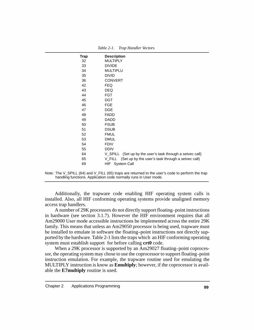
99Chapter 2 Applications Programming
Table 2-1. Trap Handler Vectors
Trap Description32 MULTIPLY33 DIVIDE34 MULTIPLU35 DIVID36 CONVERT42 FEQ43 DEQ44 FGT45 DGT46 FGE47 DGE48 FADD49 DADD50 FSUB51 DSUB52 FMUL53 DMUL54 FDIV55 DDIV64 V_SPILL (Set up by the user’s task through a setvec call)65 V_FILL (Set up by the user’s task through a setvec call)69 HIF System Call
Note: The V_SPILL (64) and V_FILL (65) traps are returned to the user’s code to perform the traphandling functions. Application code normally runs in User mode.
Additionally, the trapware code enabling HIF operating system calls isinstalled. Also, all HIF conforming operating systems provide unaligned memoryaccess trap handlers.
A number of 29K processors do not directly support floating–point instructionsin hardware (see section 3.1.7). However the HIF environment requires that allAm29000 User mode accessible instructions be implemented across the entire 29Kfamily. This means that unless an Am29050 processor is being used, trapware mustbe installed to emulate in software the floating–point instructions not directly sup-ported by the hardware. Table 2-1 lists the traps which an HIF conforming operatingsystem must establish support for before calling crt0 code.
When a 29K processor is supported by an Am29027 floating–point coproces-sor, the operating system may chose to use the coprocessor to support floating–pointinstruction emulation. For example, the trapware routine used for emulating theMULTIPLY instruction is know as Emultiply ; however, if the coprocessor is avail-able the E7multiply routine is used.

100 Evaluating and Programming the 29K RISC Family
2.2.2 crt0 Preparations before Calling main()
Application code normally begins execution at address start in the crt0.s mod-ule. The previous section described the environment prepared by a HIF conformingoperating system before the code in crt0.s is executed. The crt0.s code makes finalpreparations before the application main() procedure is called.
The code in crt0.s first copies the Am29027 shadow mode register value, passedin gr96 and gr97, to memory location __29027Mode. If a system does not have anAm29027 floating–point coprocessor then there is no useful data passed in these reg-isters. However, application code linked with floating–point libraries which makeuse of the Am29027 coprocessor, will access the shadow memory location to deter-mine the coprocessor operating mode value.
The setvec system call is then used to supply the operating system with the ad-dresses of the user’s SPILL and FILL handler code which is located in crt0.s. Be-cause this code normally runs in User mode address space, and the user has the optionto tailor the operation of this code, an operating system can not know in advance(pre–crt0.s) the required SPILL and FILL handler code operation.
When procedure main() is called, it is passed two parameters; the argc parame-ter indicates the number of elements in argv; the second parameter, argv, is a pointerto an array of the character strings:
main(argc, argv)int argc;char* argv[];
The getargs HIF service is used to get the address of the argv array. In manyreal–time applications there are no parameters passed to main(). However, to supportporting of benchmark application programs, many systems arrange for main() pa-rameters to be loaded into a user’s data space. The crt0.s code walks through thearray looking for a NULL terminating string; in so doing, it determines the argc val-ue. The register stack pointer was lowered by the start() procedure’s prologue codeto create a procedure activation record for passing parameters to main().
To aid run–time libraries a memory variable, __LibInit, is defined in uninitial-ized data memory space (BSS) by the library code. If any library code needs initial-ization before use, then the __LibInit variable will be assigned to point to a libraryroutine which will perform all necessary initialization. This is accomplished by thelinker matching–up the BSS __LibInit variable with an initialized __LibInit variabledefined in the library code. The crt0.s code checks to see if the __LibInit variablecontains a non zero address, if so, the procedure is called.
The application main() procedure is ready to be called by start(). It is not ex-pected that main() will return. Real–time programs typically never exit. However,benchmark programs do, and this is accomplished by calling the HIF exit service. If amain() routine does not explicitly call exit then it will return to start(), where exit iscalled should main() return.
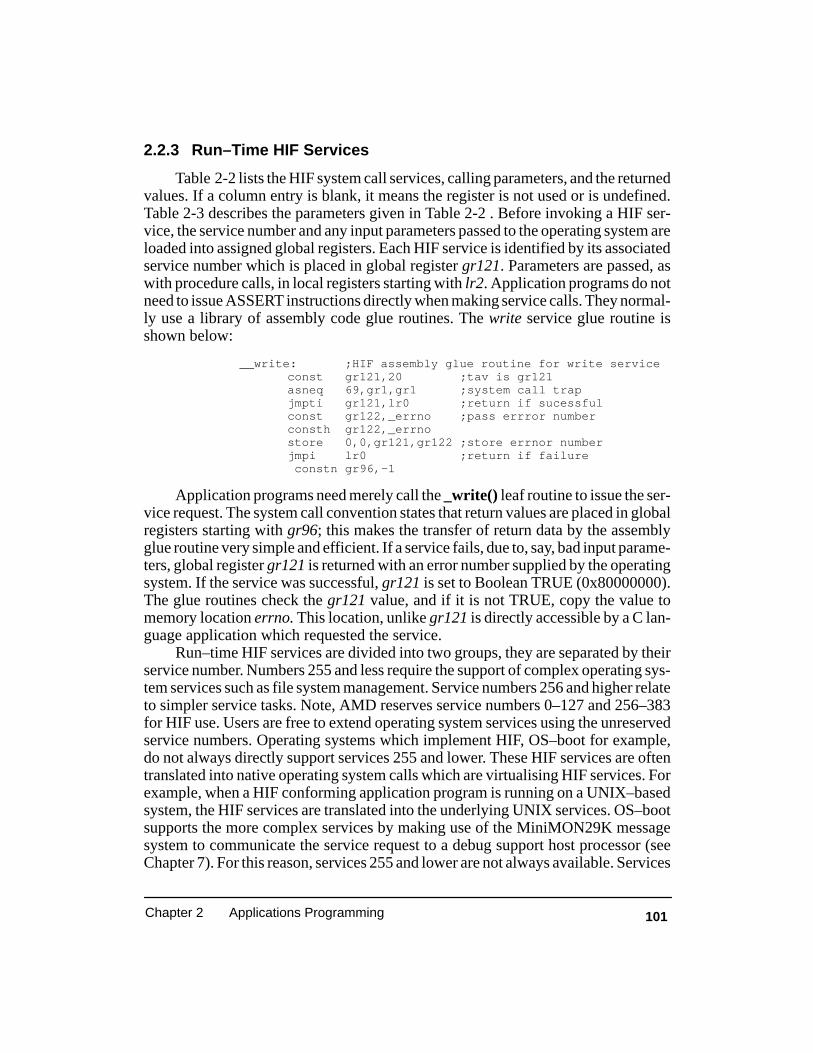
101Chapter 2 Applications Programming
2.2.3 Run–Time HIF Services
Table 2-2 lists the HIF system call services, calling parameters, and the returnedvalues. If a column entry is blank, it means the register is not used or is undefined.Table 2-3 describes the parameters given in Table 2-2 . Before invoking a HIF ser-vice, the service number and any input parameters passed to the operating system areloaded into assigned global registers. Each HIF service is identified by its associatedservice number which is placed in global register gr121. Parameters are passed, aswith procedure calls, in local registers starting with lr2. Application programs do notneed to issue ASSERT instructions directly when making service calls. They normal-ly use a library of assembly code glue routines. The write service glue routine isshown below:
__write: ;HIF assembly glue routine for write serviceconst gr121,20 ;tav is gr121asneq 69,gr1,gr1 ;system call trapjmpti gr121,lr0 ;return if sucessfulconst gr122,_errno ;pass errror numberconsth gr122,_errnostore 0,0,gr121,gr122 ;store errnor numberjmpi lr0 ;return if failure
constn gr96,–1
Application programs need merely call the _write() leaf routine to issue the ser-vice request. The system call convention states that return values are placed in globalregisters starting with gr96; this makes the transfer of return data by the assemblyglue routine very simple and efficient. If a service fails, due to, say, bad input parame-ters, global register gr121 is returned with an error number supplied by the operatingsystem. If the service was successful, gr121 is set to Boolean TRUE (0x80000000).The glue routines check the gr121 value, and if it is not TRUE, copy the value tomemory location errno. This location, unlike gr121 is directly accessible by a C lan-guage application which requested the service.
Run–time HIF services are divided into two groups, they are separated by theirservice number. Numbers 255 and less require the support of complex operating sys-tem services such as file system management. Service numbers 256 and higher relateto simpler service tasks. Note, AMD reserves service numbers 0–127 and 256–383for HIF use. Users are free to extend operating system services using the unreservedservice numbers. Operating systems which implement HIF, OS–boot for example,do not always directly support services 255 and lower. These HIF services are oftentranslated into native operating system calls which are virtualising HIF services. Forexample, when a HIF conforming application program is running on a UNIX–basedsystem, the HIF services are translated into the underlying UNIX services. OS–bootsupports the more complex services by making use of the MiniMON29K messagesystem to communicate the service request to a debug support host processor (seeChapter 7). For this reason, services 255 and lower are not always available. Services

102 Evaluating and Programming the 29K RISC Family
exit 1 exitcode Service does not returnopen 17 pathname mode pflag fileno errcodeclose 18 fileno retval errcodread 19 fileno buffptr nbytes count errcode
write 20 fileno buffptr nbytes count errcodelseek 21 fileno offset orig where errcoderemove 22 pathname retval errcoderename 23 oldfile newfile retval errcodeioctl 24 fileno mode errcodeiowait 25 fileno mode count errcodeiostat 26 fileno iostat errcodetmpnam 33 addrptr filename errcodetime 49 secs errcodegetenv 65 name addrptr errcodegettz 67 zonecode dstcode errcode
sysalloc 257 nbytes addrptr errcodesysfree 258 addrptr nbytes retval errcode
getpsize 259 pagesize errcodegetargs 260 baseaddr errcodeclock 273 msecs errcodecycles 274 LSBs cycles MSBs cycles errcodesetvec 289 trapno funaddr trapaddr errcodesettrap 290 trapno trapaddr trapaddr errcodesetim 291 mask di mask errcodequery 305 capcode hifvers errcode
capcode cpuvers errcodecapcode 027vers errcodecapcode clkfreq errcodecapcode memenv errcode
signal 321 newsig oldsig errcodesigdfl 322 [gr125 points to HIF signal frame] Service does not returnsigret 323 [gr125 points to HIF signal frame] Service does not returnsigrep 324 [gr125 points to HIF signal frame] Service does not returnsigskp 325 [gr125 points to HIF signal frame] Service does not returnsendsig 326 sig errcode
Title gr121 gr121gr97gr96lr2 lr3 lr4
Table 2-2. HIF Service Calls
Service Calling Parameters Returned Values
with numbers 256 and higher do not require the support of a remote host processor.These services are implemented directly by OS–boot. If an underlying operating sys-tem, such as UNIX, is being used, then some of these services may not be available asthey may violate the underlying operating system’s security.

103Chapter 2 Applications Programming
When application benchmark programs use HIF services, care should be taken.If a program requests a service such as time (service 49) it will suffer the delays ofcommunicating the service request to a remote host if the OS–boot operating systemis used. This can greatly effect the performance of a program, as execution will bedelayed until the remote host responds to the service request. It is better to use ser-vices such as cycles (service 274) or clock (service 273) which are executed by the29K processor and do not suffer the delays of remote host communication.
The assembly level glue routines for HIF services 255 and lower are rarely re-quested directly by an application program. They are more frequently called upon bylibrary routines. For example, use of the library printf() routine is the typical way ofgenerating a write HIF service request. The mapping between library routines andHIF services may not be always direct. The printf() routine, when used with a deviceoperating in COOKED mode, may only request write services when flushing bufferssupporting device communication. Appendix A contains a detailed description ofeach HIF service in terms of input and output parameters, as well as error codes.
2.2.4 Switching to Supervisor Mode
Operating systems which conform to HIF normally run application code in Usermode. However, many real–time applications require access to resources which arerestricted to Supervisor mode. If the HIF settrap service is supported, it is easy toinstall a trap handler which causes application code to commence execution in Su-pervisor mode. The example code sequence below uses the settrap() HIF library rou-tine to install a trap handler for trap number 70. The trap is then asserted using assem-bly language glue routine assert_70().
extern int super_mode();/* Here in User mode */_settrap(70,super_mode);/* install trap handler */assert_70(); /* routine to assert trap */. . . /* Here in Supervisor mode */
The trap handler is shown below. Its operation is very simple; it sets the Supervi-sor mode bit in the old processors status registers (OPS) before issuing a trap returninstruction (IRET). Other application status information is not affected. For exam-ple, if the application was running with address translation turned on, then it will con-tinue to run with address translation on, but now in Supervisor mode.
In fact the example relies on application code running with physical addressing;or if the Memory Management Unit is used to perform address translation, then virtu-al addresses are mapped directly to physical addresses. This is because the Freezemode handler, super_mode(), runs in Supervisor mode with address translationturned off. But the settrap system call, which installs the super_mode() handler ad-dress, runs in User mode and thus operates with User mode address values.

104 Evaluating and Programming the 29K RISC Family
.global _super_mode_super_mode: ;gr64 is an OS temporary
mfsr gr64,ops ;read the OPS registeror gr64,gr64,0x10 ;set SM bit in OPSmtsr ops,gr64 ;iret back to Supervisor modeiret
The super_mode() and assert_70() routines have to be written in assembly lan-guage. The IRET instruction in super_mode() starts execution of the JMPI instruc-tion in the assert_70() routine shown below. The method shown of forcing a trap canbe used to test a systems interrupt and trap support software.
.global _assert_70_assert_70: ;leaf routine
asneq 70,gr96,gr96 ;force trap 70jmpi lr0 ;return nop
Table 2-3. HIF Service Call Parameters
Parameter Description
027vers The version number of the installed Am29027 arithmetic accelerator chip (if any)addrptr A pointer to an allocated memory area, a command-line-argument array, a path-
name buffer, or a NULL-terminated environment variable name string.baseaddr The base address of the command-line-argument vector returned by the getargs
service.buffptr A pointer to the buffer area where data is to be read from or written to during the
execution of I/O services, or the buffer area referenced by the wait service.capcode The capabilities request code passed to the query service. Code values are: 0 (re-
quest HIF version), 1 (request CPU version), 2 (request Am29027 arithmetic accel-erator version), 3 (request CPU clock frequency), and 4 (request memory environ-ment).
clkfreq The CPU clock frequency (in Hertz) returned by the query service.count The number of bytes actually read from file or written to a file.cpuvers The CPU family and version number returned by the query service.cycles The number of processor cycles (returned value).di The disable interrupts parameter to the setim service.dstcode The daylight savings time in effect flag returned by the gettz service.errcode The error code returned by the service. These are usually the same as the codes
returned in the UNIX errno variable.exitcode The exit code of the application program.
(continued)
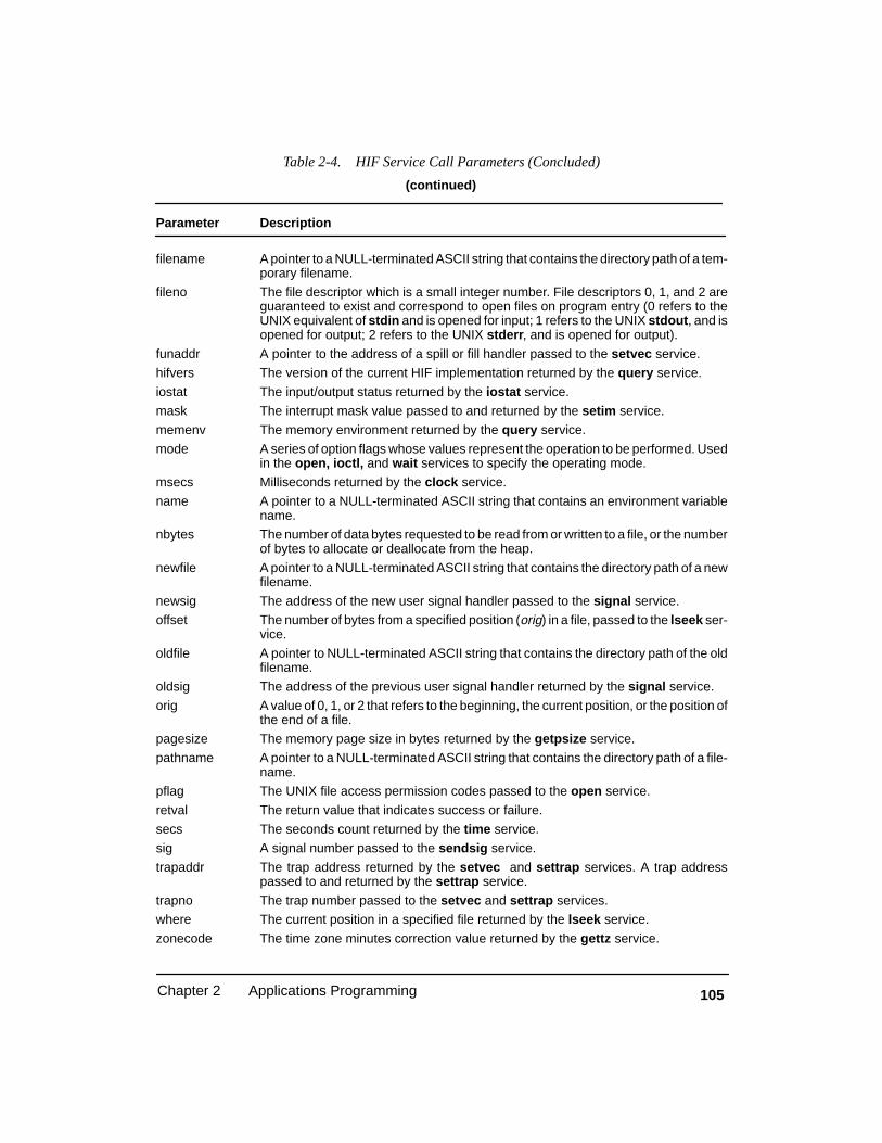
105Chapter 2 Applications Programming
Table 2-4. HIF Service Call Parameters (Concluded)
(continued)
Parameter Description
filename A pointer to a NULL-terminated ASCII string that contains the directory path of a tem-porary filename.
fileno The file descriptor which is a small integer number. File descriptors 0, 1, and 2 areguaranteed to exist and correspond to open files on program entry (0 refers to theUNIX equivalent of stdin and is opened for input; 1 refers to the UNIX stdout , and isopened for output; 2 refers to the UNIX stderr , and is opened for output).
funaddr A pointer to the address of a spill or fill handler passed to the setvec service.
hifvers The version of the current HIF implementation returned by the query service.
iostat The input/output status returned by the iostat service.
mask The interrupt mask value passed to and returned by the setim service.
memenv The memory environment returned by the query service.
mode A series of option flags whose values represent the operation to be performed. Usedin the open, ioctl, and wait services to specify the operating mode.
msecs Milliseconds returned by the clock service.
name A pointer to a NULL-terminated ASCII string that contains an environment variablename.
nbytes The number of data bytes requested to be read from or written to a file, or the numberof bytes to allocate or deallocate from the heap.
newfile A pointer to a NULL-terminated ASCII string that contains the directory path of a newfilename.
newsig The address of the new user signal handler passed to the signal service.
offset The number of bytes from a specified position (orig) in a file, passed to the lseek ser-vice.
oldfile A pointer to NULL-terminated ASCII string that contains the directory path of the oldfilename.
oldsig The address of the previous user signal handler returned by the signal service.
orig A value of 0, 1, or 2 that refers to the beginning, the current position, or the position ofthe end of a file.
pagesize The memory page size in bytes returned by the getpsize service.
pathname A pointer to a NULL-terminated ASCII string that contains the directory path of a file-name.
pflag The UNIX file access permission codes passed to the open service.
retval The return value that indicates success or failure.
secs The seconds count returned by the time service.
sig A signal number passed to the sendsig service.
trapaddr The trap address returned by the setvec and settrap services. A trap addresspassed to and returned by the settrap service.
trapno The trap number passed to the setvec and settrap services.
where The current position in a specified file returned by the lseek service.
zonecode The time zone minutes correction value returned by the gettz service.
106 Evaluating and Programming the 29K RISC Family
2.3 C LANGUAGE COMPILER
I know of six C language compilers producing code for the 29K family. Themost widely used of these are: the High C 29K compiler developed by Metaware Inc;and GNU supported by the Free Software Foundation and Cygnus Support Inc. De-velopers of 29K software normally operate in a cross development environment,editing and compiling code on one machine which is intended to run on 29K targethardware. The High C 29K compiler is sold by a number of companies, includingAMD, and packaged along with other vendor tools. High C 29K can produce codefor both big– and little–endian 29K operation. The GNU compiler, gcc, currently(version 2.5) produces big–endian code. This does not present a problem as the 29Kis used predominantly in big–endian.
2.3.1 Compiler Optimizations
A RISC chip is very sensitive to code optimization. This is not surprising sincethe RISC philosophy gives software greater access to a processor’s internals relativeto most CISC processors. Compilers make use of a number of code optimizationtechniques which it is difficult for the assembly language programmer to consistentlymake use of. Some of these techniques are briefly described below. For example:
Common Sub–Expression Elimination
... c=a+b;...d=a+b; /* sub-expression used again */...
The expression a+b is a common sub-expression, it does not need to be eva-luated twice. A more efficient compiler would store the result of the first evaluationin a local or global register and reuse the value in the second expression. Temporaryvariables used during interim calculations are optimized by the compiler. These com-piler-generated temporaries are allocated to register cache locations.
Strength Reduction
When ever possible “strength reduction” is performed. This refers to replacingexpensive instructions with less expensive ones. For example, replace multiplies byfactors of two with more efficient shift instructions.
Loop Invariant Code Motion
Sometimes a C programmer will place code in a loop which could have beenlocated outside of the loop. For example, variable initialization need not be repeated-

107Chapter 2 Applications Programming
ly executed in a loop. The loop invariant initialization would be located before theloop code. Hence, the amount of code required to support each loop iteration is mini-mized.
Loop UnrollingThere are a number of optimization techniques applicable to code loops. The
objective is the same, to replace the loop with a sequence of faster executing code.This often involves unrolling the loop partially or completely. For example, thecompiler may determine a loop is traversed, say, three times. It may be more effectiveto replace the loop with three in–line versions of the loop. This would eliminate thebranching required by the loop. Additionally, when a loop is unrolled there aregenerally increased opportunities to apply optimizations not available to the loopedalternative. Consequently, sections on the expanded loop need not be justduplications of a single loop iteration, but something smaller and more registerefficient.
Dead–Code EliminationCode which can never be executed is eliminated. This saves on memory usage.
Unexecutable code can result from a branch which can never be taken. Compilersgenerally issues a warning when they detect “unreachable code”. Additionally, resultvalues which are never used can be eliminated; this can remove unneeded storeinstructions.
Improved Register AllocationA processor’s registers are a critical resource in determining performance.
Accessing registers is very much more efficient than accessing off–chip memory.The ability of the compiler to devise schemes to keep data within the availableregisters is critical. Additionally, given that the 29K compiler determines the size of aprocedure’s register window, it is important to minimize register allocation if spillingand filling are to be avoided.
Constant Propagation And Folding Variables are often assigned constant values. Later, the variable is used in a cal-
culation. The 29K instruction format supports 8–bit immediate data constants. Ap-plying constant variables as immediate data rather than holding the variable in a reg-ister can be more efficient. Additionally, propagating an immediate value may enableit to be combined with another immediate value at compile time. This is better thanperforming a run–time calculation.
Register–to–Register Copying (Copy Propagation) When examining compiler generated code, particularly if the target is a CISC
processor, it is not unusual to see stores of register data to memory locations. This

108 Evaluating and Programming the 29K RISC Family
makes the register available for reuse. Later, the stored data is reloaded for furtherprocessing. The better RISC compilers try to keep data in registers longer; and useregister–to–register copying rather than register–to–memory.
Memory ShadowingThe performance impact of a memory access is reduced when the access is per-
formed to a copy–back data cache. However, most processors do not have this advan-tage available to them. The term “memory shadowing” refers to the increased use ofregisters for data variable storage. Again, directing accesses to registers rather thanoff–chip memory has significant performance advantages. Of course, if a variable isdefined volatile it can not be held in a register.
Memory References Are Coalesced and AlignedData memory can be most efficiently accessed using burst–mode addressing.
This requires the use of load– and store–multiple instructions. When a sufficientlylarge data object is being moved between memory and registers, it is best to use theburst–mode supported instructions. The compiler can also arrange for frequently ac-cessed data to be located (coalesced) in adjacent memory locations, even if the datavariables were not consecutively defined.
There are also performance benefits to be had by aligning target instructions oncache block boundaries. For example, a procedure can be aligned to start on a 4–wordboundary. This improves cache utilization and performance –– particularly withcaches which do not support partially filled cache blocks.
Delay Slot FillingThe compilers perform “delay slot filling” (see section 3.1.8). Delay slots occur
whenever a 29K processor experiences a disruption in consecutive instruction execu-tion. The processor always executes the instruction in the decode pipeline stage, evenif the execute stage contains a jump instruction. Delay slot is the term given to theinstruction following the jump or conditional branch instruction. Effectively, thebranch instruction is delayed one cycle. Unlike assembly language programmers, thecompiler easily finds useful instructions to insert after branching instructions. Theseinstructions, which are executed regardless of the branch condition, are effectivelyachieved at no cost. Typically, an instruction that is invariant to the branch outcome ismoved into the delay slot just after the branch or jump instruction.
Jump Optimizations Because of the pipeline stalling effects of jump instruction, scheduling these
instructions can achieve significant performance improvements. The objective is toreduce the number of taken branches. For example, code loops typically have condi-tional tests at the top of the loop to test for loop completion. This results in branchinstructions at the top and the bottom of the loop. If the conditional branch is movedto the bottom of the loop then the number of branches is reduced.

109Chapter 2 Applications Programming
Instruction Scheduling
The 29K allows load and store instructions to be overlapped with other instruc-tions that do not depend on the load or store data. Ordinarily, a processor will loaddata into a register before it makes use of it in the subsequent instruction. To enableoverlapping of the external memory access, the load instruction must be executed atan earlier stage, before it is required. Best results are obtained if code motion tech-niques are used to push the load instruction back by as many instructions as there arememory access delay cycles (another name for this technique is instruction pre-scheduling). This will prevent processor pipeline stalling caused by an operand valuenot being available. Once again, code motion is best left to the compiler to worryabout.
Leaf Procedure Optimization
Leaf procedures are procedures which do not call other procedures; at least theydo not contain any C level procedure calls. However, they can contain transparentroutine calls inserted by the compiler. Because of this unique characteristic of leafroutines, a number of optimizations can be applied. For example, simplifiedprocedure prologue and epilogue, alternative register usage. When a leaf is static inscope (only known within the defining module) alternative parameter passing andregister allocation schemes can be applied.
With newer versions of the High C 29K compiler, it is possible to constructsimple procedures as transparent routines (see section 3.7). If a procedure qualifiesfor a transparent–type implementation, then its parent (in the calling sequence) mayitself become a leaf procedure. This propagates the benefits obtained by leafprocedures.
In–lining Simple Functions
The program may call a procedure but the compiler can replace the call withequivalent in–line code. For very small procedures this can be a performanceadvantage. However, as the called procedure grows in size and in–lining is frequentlyapplied, then code space requirements will increase. In–lining is frequently utilizedwith C++ code which often has classes with small member functions. The registerrequirements of a procedure can grow when it has to deal with in–line code ratherthan a procedure call. This does not present much difficulty for a 29K processor as itcan individually tailor the register allocation to each procedure’s requirements withdynamically sized register windows.
As stated above, it is possible to construct simple functions as transparentroutines (see section 3.7). This is not really in–lining, but it does further reduce theoverhead associated with even a leaf procedure. Additionally, placing code in atransparent routine, which is shared, helps reduce the code expansion which occurswith in–lining. For this reason using the C language key word _Transparent to define

110 Evaluating and Programming the 29K RISC Family
the type of small procedures, may be a performance advantage when used with C++object member functions.
Global Function In–lining
When code in–lining is applied, it is typically limited to functions defined andused within an single module. More elaborate schemes enable a function to bedefined in one module and the related code to be inserted in–line even if the call to thefunction appears in another file. Applying function in–lining in this global fashioncan greatly extend the benefits of in–lining.
Two–pass Code Compilation
Most compilers apply their optimization statically. That is entirely at compiletime. However, by observing the program in execution, optimizations can be furtherrefined. For example, branch prediction can be applied statically, but observing thefrequency of actual branching reveals the most traversed code paths. Additionally,the data which is most frequently accessed can be determined. With this informationa second pass of the compiler can be applied and further code optimizations incorpo-rated.
Superblock Formation
Software optimizations are normally only applied within a code block. A blockis a code sequence which is bounded by a single entry point (at the top –– a loweraddress) and one or more exit points (a jump or call instruction). Instructionscheduling and other optimizations can be better utilized if an instruction block islarge. For this reason techniques which enlarge a block’s size and create a superblockare important
A superblock may contain a number of basic blocks, yet code optimizations canbe applied over the larger superblock code sequence. Creation of a superblock canrequire duplication of code. Typically the tail of a superblock will be duplicated (tailrecursion) to eliminate side entry points to the superblock. Optimization techniqueswhich help superblock creation are: loop unrolling, function in–lining, jumpelimination, code duplication, code migration, and code profiling.
2.3.2 Metaware High C 29K Compiler
The Metaware Inc. compiler, invoked with the hc29 driver, has held the positionas the top performing 29K compiler for a number of years. It generally produces thefastest code, which is of the smallest size. It is available on SUN and HP workstationplatforms as well as IBM PC–AT machines. It may be made available on other plat-forms depending on customer demand. A number of companies resell the compileralong with other tools, such as debuggers and emulators.
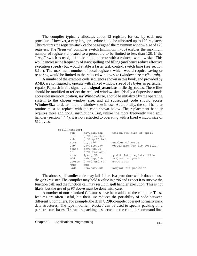
111Chapter 2 Applications Programming
The compiler typically allocates about 12 registers for use by each newprocedure. However, a very large procedure could be allocated up to 128 registers.This requires the register–stack cache be assigned the maximum window size of 128registers. The “lregs=n” compiler switch (minimum n=36) enables the maximumnumber of registers allocated to a procedure to be limited to less than 128. If the“lregs” switch is used, it is possible to operate with a reduced window size. Thiswould increase the frequency of stack spilling and filling (and hence reduce effectiveexecution speeds) but would enable a faster task context switch time (see section8.1.4). The maximum number of local registers which would require saving orrestoring would be limited to the reduced window size (window size = rfb – rab).
A number of the example code sequences shown in this book, and provided byAMD, are configured to operate with a fixed window size of 512 bytes; in particular,repair_R_stack in file signal.s and signal_associate in file sig_code.s. These filesshould be modified to reflect the reduced window size. Ideally a Supervisor modeaccessible memory location, say WindowSize, should be initialized by the operatingsystem to the chosen window size, and all subsequent code should accessWindowSize to determine the window size in use. Additionally, the spill handlerroutine must be replace with the code shown below. The replacement handlerrequires three additional instructions. But, unlike the more frequently used spillhandler (section 4.4.4), it is not restricted to operating with a fixed window size of512 bytes.
spill_handler:sub tav,rab,rsp ;calculate size of spillsrl gr96,tav,0x2sub gr96,gr96,0x1mtsr cr,gr96 ;number of wordssub tav,rfb,tav ;determine new rfb positionconst gr96,0x200or gr96,tav,gr96mtsr ipa,gr96 ;point into register fileadd rab,rsp,0x0 ;adjust rab positionstorem 0,0x0,gr0,tav ;move datajmpi tpc add rfb,tav,0x0 ;adjust rfb position
The above spill handler code may fail if there is a procedure which does not usethe gr96 register. The compiler may hold a value in gr96 and expect it to survive thefunction call; and the function call may result in spill handler execution. This is notlikely, but the use of gr96 above must be done with care.
A number of non–standard C features have been added to the compiler. Thesefeatures are often useful, but their use reduces the portability of code betweendifferent C compilers. For example, the High C 29K compiler does not normally packdata structures. The type modifier _Packed can be used to specify packing on aper–structure bases. If structure packing is selected on the compiler command line,
112 Evaluating and Programming the 29K RISC Family
unpacked structures can be selectively specified with the _Unpacked type modifier.For example:
typedef _Packed struct packet_str /* packed structure */{ char A;
int B;. . .
} packet_t;
A HIF conforming operating systems provides unaligned memory access traphandlers –– any 29K operating system may choose to do this. Hence, if an object larg-er than a byte is accessed and the object is not aligned to an object–sized boundary,then a trap will be taken and the trap handler will perform the required access instages if necessary. The trap handler will require several processor cycles to performits task. To the programmer, the required data is accessed as if it were aligned on thecorrect address boundary. In the example above, structure member B is of size int butis not aligned on a int–sized boundary (given object A is a char and it is aligned on aword–sized boundary).
Of course there is a performance penalty for use of trap handlers. For this reason,packed data structures are seldom used. However, there use does reduce datamemory requirements, and for this reason data is often sent between processors inpacked data packets. When a data packet is received, its contents can be accessed asbytes without any data alignment difficulties. Access of data larger than bytes mayrequire unaligned trap handler support, and thus suffer a performance penalty.
The High C 29K compiler offers a solution to the performance problem with thetype modifiers _ASSUME_ALIGNED and _ASSUME_UNALIGNED. They enable apointer to a unaligned structure to be declared. For example:
receive_packet(packet_p)_ASSUME_UNALIGNED packet_t* packet_p;{
int data = packet_p–>B;/* unaligned access */. . .
The receive_packet() procedure is passed a pointer to a data structure which isknown to be unaligned. Normally, when member B of the packet structure isaccessed, an unaligned trap occurs. However, informing the compiler of theunaligned nature of the data enables the compiler to replace the normal loadinstruction used to read the B data with a transparent helper routine call (see section3.7). The transparent helper routine performs the same task as the trap handler butwith a reduced overhead.
2.3.3 Free Software Foundation, GCC
The GNU compiler, gcc, can be obtained from any existing users who are in aposition, and has the time, to duplicate their copy. Alternatively, the Free Software

113Chapter 2 Applications Programming
Foundation can be contacted. For a small fee, Cygnus Support Inc. will ship you acopy along with their documentation. The GNU compiler is available in source form,and currently runs on UNIX type host machines as well as 386 based IBM PCs andcompatibles.
Considering the Stanford University benchmark suite, the gcc compiler (ver-sion 2.3) produces code which is on average 15–20% slower in execution comparedto hc29. The GNU compiler also used considerably more memory to contain thecompiled code. Of course your application program may experience somewhat dif-ferent results.
2.3.4 C++ Compiler Selection
Programmers first started developing C++ code for the 29K in 1988; they usedthe AT&T preprocessor, cfront, along with the High C 29K compiler. A number ofsupport utilities were developed at that time to enable the use of cfront: nm29,munch29, and szal29, which gave the size and alignment of 29K data objects (re-quired for cross development environments).
Because the GNU tool chains can support C++ code development directly withthe the GCC compiler there is little use being made of the AT&T cfront preprocessor.Additionally, MRI and Metaware have recently announced upgrades to their prod-ucts which now enable C++ code development. (C++ makes extensive use of dynam-ic memory resources, see section 2.4.1.)
2.3.5 Executable Code and Source Correspondence
The typically high levels of optimization applied by a compiler producing codefor RISC execution, can make it difficult to identify the relationship between 29Kinstructions and the source level code. When looking at the 29K instructionsproduced by the compiler, it is not always easy to identify the assembly instructionswhich correspond to each line of C code. Optimizations such as: code motion,sub–expression elimination, loop unrolling, instruction scheduling and more, all addto the difficulty.
Fortunately, there is usually little need to study the resulting instructionsproduced after compilation. However, it can occasionally be worth studyingcompiler output when trying to understand the performance of critical codesegments. It is difficult to obtain a small example of C code which demonstrates allthe potential code optimizations. The example below is interesting, but illustratesonly a few of the difficulties of relating source code to 29K instructions.
int strcmp(s1, s2) /* file strcmp.c */char *s1,*s2;{
114 Evaluating and Programming the 29K RISC Family
int cnt=0;for(cnt=0;;cnt++);{ if(s1[cnt]!=s2[cnt])
return –1;if(s1[cnt]==’\0’ || s2[cnt]==’\0’) /* line 8 */
if(s1[cnt]==’\0’ && s2[cnt]==’\0’)return 0;
elsereturn –1;
}} /* line 14 */
The procedure, strcmp(), is similar to the ANSI library routine of the samename. It is passed the address of two strings. The strings are compared to determine ifthey are the same. If they are the same, zero is returned, otherwise –1 is returned. Thisis not exactly the same behavior as the ANSI routine.
The procedure is based on a for–loop statement which compares characters inthe two strings until they are found to be different or one of the strings is terminated.The algorithm used by the C code is not optimal. But this makes the example moreinteresting as it challenges the compiler to produce the minimum code sequence. TheMetaware compiler was first used to compile the code with a high level ofoptimization selected (–O7). The command line use was “hc29 –S –Hanno –O7strcmp.c”. The “–S” switch causes the compiler to stop after it has produced 29Kassembly code –– no linking with libraries is performed. The “–Hanno” switchcauses the source C code to be embedded in the output assembly code. This helpsidentify the assembly code corresponding to each line of C code. The assembly codeproduced is shown below. Note that some assembly level comment statements havebeen added to help explain the code operation.
.text
.word 0x40000 ; Tag: argcnt=2 msize=0
.global _strcmp_strcmp:;4 | int cnt=0;;5 | for(cnt=0;;cnt++)
jmp L2 const gr97,0 ;cnt=0
L3: ;top of for–loopL2:;6 | { if(s1[cnt]!=s2[cnt])
add gr96,lr2,gr97load 0,1,gr99,gr96 ;load s1[cnt]add gr96,lr3,gr97load 0,1,gr98,gr96 ;load s2[cnt]cpeq gr96,gr99,gr98 ;compare charactersjmpf gr96,L4 ; jump if different cpeq gr96,gr99,0 ;test if s1[cnt] == ’\0’
;8 | if(s1[cnt]==’\0’ || s2[cnt]==’\0’)jmpt gr96,L5 ; jump if string end cpneq gr96,gr98,0 ;test s2[cnt]

115Chapter 2 Applications Programming
jmpt gr96,L3 ;for–loop if not end add gr97,gr97,1 ;increment cnt
L5:;9 | if(s1[cnt]==’\0’ && s2[cnt]==’\0’)
cpneq gr96,gr99,0 ;here is at end of stringjmpt gr96,L4 ;jump if s1[]!=’\0’ cpneq gr96,gr98,0jmpt gr96,L7 ;jump if s2[]!=’\0’ constn gr96,–1
;10 | return 0;jmpi lr0 ;strings match const gr96,0 ;return 0
L4:constn gr96,–1 ;no match
L7:;12 | return –1;
jmpi lr0 nop
The body of the for–loop is contained between address labels L3 and L5. Thecompiler has filled the delay slot of jump instructions with other useful instructions.Within the for–loop, LOAD instruction are used to access the characters of eachstring. Register gr97 is used to hold the loop–count value, cnt. The count value isincremented each time round the for–loop. The value in gr97 is added to the base ofeach string (lr2 and lr3) to obtain the address of each character required for compari-son. The LOAD instructions have been scheduled to somewhat reduce conflict foroff–chip access and reduce the pipeline stalling affects of LOAD instructions.
Within the body of the loop three tests are applied: one to determine if the char-acters at the current position in the string match; the remaining two, to determine ifthe termination character has been reached for either of the strings. The assemblycode after label L5 selects the correct return value when the tested characters do notmatch or string termination is reached. There is unnecessary use of jump instructionsin the code following label L5 and also in the initial code jumping to label L2. It issomewhat fortunate that this less optimal code does not appear within the more fre-quently executed for–loop body.
The same code was compiled with the GNU compiler using command “gcc –S–O4 strcmp.c”. The assembly code produced is shown below; it is quite differentfrom the Metaware produced code.
.text
.align 4
.global _strcmp
.word 0x40000_strcmp:L2: ;top of for–loop
load 0,1,gr117,lr2 ;load s1[cnt]load 0,1,gr116,lr3 ;load s2[cnt]cpneq gr116,gr117,gr116 ;compare charactersjmpf gr116,L5 ;jump if match

116 Evaluating and Programming the 29K RISC Family
cpneq gr116,gr117,0 ;test for s1[] endjmpi lr0 ;no match constn gr96,65535 ; return –1
L5: ;here if s1[cnt]==s2[cnt]jmpfi gr116,lr0 ;return if at string end const gr96,0add lr3,lr3,1 ;next s2[] characterjmp L2 ;for–loop add lr2,lr2,1 ;next s1[] character
All of the code is contained in the body of the for–loop. A for–loop transitionconsists of 10 instructions, a decrease of one compared to the Metaware code. How-ever, LOAD instructions are now placed back–to–back, and loaded data is used im-mediately. Additionally, the normal path through the for–loop contains an additionaljump to label L5. This will increase the actual number of cycles required to execute asingle for–loop to more than 10 cycles. It is likely the Metaware produced code willexecute in a shorter time.
No register (previously gr97) is used to contain the cnt value. The pointers to thepassed strings, lr2 and lr3, are advanced to point to the next character within the for–loop. Delay slot instructions are productively filled and there are no unnecessaryjump instructions.
Lines 8 through 12 of the source code are only applied if the tested characters arefound not to match. Consequently, it is redundant to test if either string has reachedthe termination character –– if one has, they both have. This optimization shouldhave been reflected in the source code. However, the GNU compiler has identifiedthat it need only test string s1[] for termination. This results in the elimination of 29Kinstructions relating to later C code lines. For example, there is no code relating to theif–statement on line 9. If an attempt is made to place a breakpoint on source line 9using the GDB source level debugger, then no breakpoint will be installed. Other de-buggers may give a warning message or place a breakpoint at the first line before orafter the requested source line.
Programmers familiar with older generation compilers applied to CISC codegeneration will notice the increased complexity in associating 29K instructions tosource C statements –– even for the simple example shown. As procedures becomelarger and more complex, code association become increasingly more difficult. Thequality of 29K code produced by the better compilers available, make it very difficultto consistently (or frequently) produce better code via hand crafting 29K instruc-tions. Because of the difficulty of understanding the compiler generated code, it isbest to only incorporate hand–built code as separate procedures which comply withthe C language calling convention.
2.3.6 Linking Compiled Code
After application code modules have been compiled or assembled, they must belinked together to form an executable file. There are three widely used linker tools:
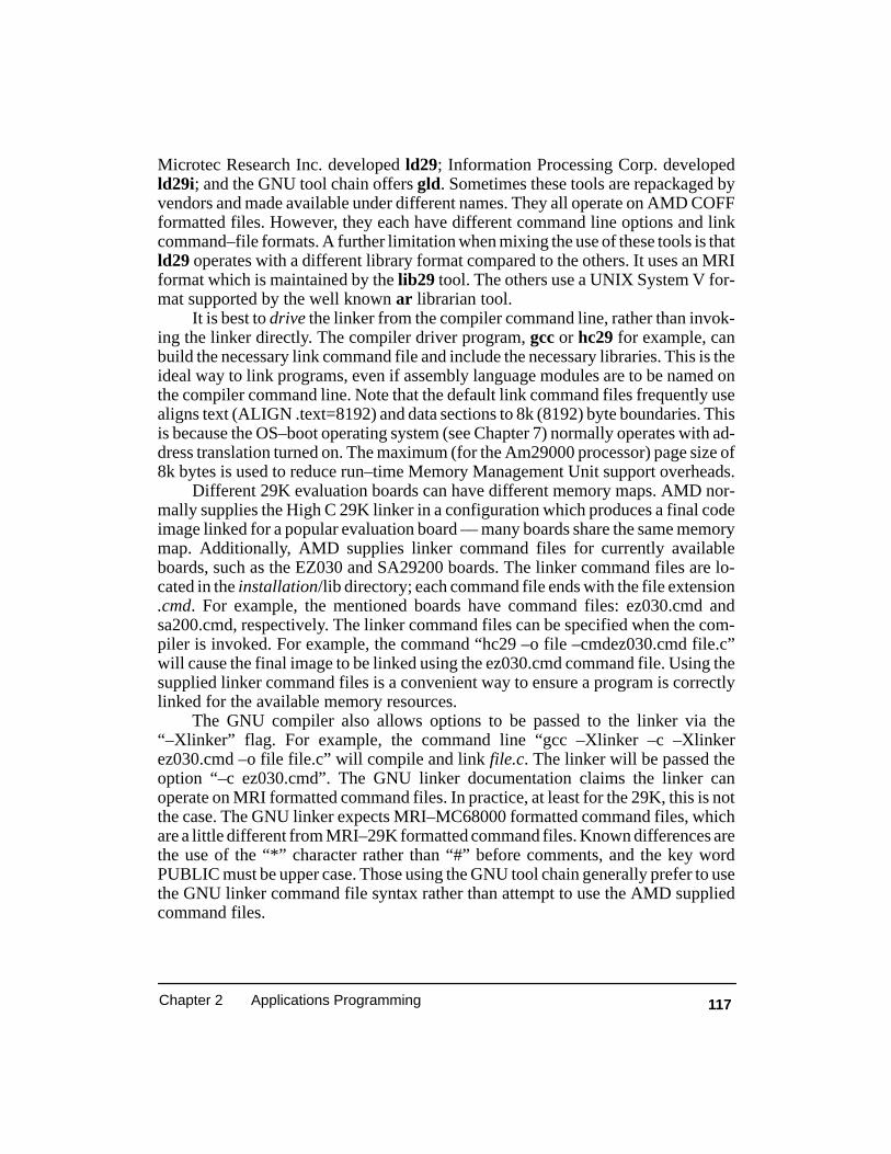
117Chapter 2 Applications Programming
Microtec Research Inc. developed ld29; Information Processing Corp. developedld29i; and the GNU tool chain offers gld. Sometimes these tools are repackaged byvendors and made available under different names. They all operate on AMD COFFformatted files. However, they each have different command line options and linkcommand–file formats. A further limitation when mixing the use of these tools is thatld29 operates with a different library format compared to the others. It uses an MRIformat which is maintained by the lib29 tool. The others use a UNIX System V for-mat supported by the well known ar librarian tool.
It is best to drive the linker from the compiler command line, rather than invok-ing the linker directly. The compiler driver program, gcc or hc29 for example, canbuild the necessary link command file and include the necessary libraries. This is theideal way to link programs, even if assembly language modules are to be named onthe compiler command line. Note that the default link command files frequently usealigns text (ALIGN .text=8192) and data sections to 8k (8192) byte boundaries. Thisis because the OS–boot operating system (see Chapter 7) normally operates with ad-dress translation turned on. The maximum (for the Am29000 processor) page size of8k bytes is used to reduce run–time Memory Management Unit support overheads.
Different 29K evaluation boards can have different memory maps. AMD nor-mally supplies the High C 29K linker in a configuration which produces a final codeimage linked for a popular evaluation board –– many boards share the same memorymap. Additionally, AMD supplies linker command files for currently availableboards, such as the EZ030 and SA29200 boards. The linker command files are lo-cated in the installation/lib directory; each command file ends with the file extension.cmd. For example, the mentioned boards have command files: ez030.cmd andsa200.cmd, respectively. The linker command files can be specified when the com-piler is invoked. For example, the command “hc29 –o file –cmdez030.cmd file.c”will cause the final image to be linked using the ez030.cmd command file. Using thesupplied linker command files is a convenient way to ensure a program is correctlylinked for the available memory resources.
The GNU compiler also allows options to be passed to the linker via the“–Xlinker” flag. For example, the command line “gcc –Xlinker –c –Xlinkerez030.cmd –o file file.c” will compile and link file.c. The linker will be passed theoption “–c ez030.cmd”. The GNU linker documentation claims the linker canoperate on MRI formatted command files. In practice, at least for the 29K, this is notthe case. The GNU linker expects MRI–MC68000 formatted command files, whichare a little different from MRI–29K formatted command files. Known differences arethe use of the “*” character rather than “#” before comments, and the key wordPUBLIC must be upper case. Those using the GNU tool chain generally prefer to usethe GNU linker command file syntax rather than attempt to use the AMD suppliedcommand files.

118 Evaluating and Programming the 29K RISC Family
When developing software for embedded applications there is always the prob-lem of what to do with initialized data variables. The problem arises because vari-ables must be located in RAM, but embedded programs are typically not loaded by anoperating system which prepares the data memory locations with initialized values.Embedded programs are stored in ROM; this means there is no problem with pro-gram instructions unless a program wishes to modify its own code at run–time.
Embedded system support tools typically provide a means of locating initial-ized data in ROM; and transferring the ROM contents to RAM locations before pro-gram execution starts. The High C 29K linker, ld29, provides the INITDATA com-mand for this purpose. Programs must be linked such that all references to writeabledata occur to RAM addresses. The INITDATA scans a list of sections and transfersthe data variables found into a new .initdat section. The list contains the names ofsections containing initialized data. The linker is then directed to locate the new .init-data section in ROM.The start address of the new section is marked with symbolinitdat .
Developers are provided with the source to a program called initcopy() whichmust be included in the application program. This program accesses the data in ROMstarting at label initdat and transfers the data to RAM locations. The format of thedata located in the .initdat section is understood by the initcopy() routine. This rou-tine must be run before the application main() program. A user could place a call tothe initialization routine inside crt0.s.
Note, because initcopy() must be able to read the appropriate ROM devices,these devices must be placed in an accessible address space. This is not a problem for2–bus members of the 29K family, but 3–bus members can have a problem if the .in-itdat section is located in a ROM device along with program code. Processors with3–bus architectures, such as the Am29000, have separately addressed Instructionand ROM spaces which are used for all instruction accesses. The Am29000 proces-sor has no means of reading these two spaces to access data unless an external bridgeis provided. If program code and initialized data are located in the same ROM device,the initcopy() program can only be used if an external bridge is provided. This bridgeconnects the Am29000 processor data memory bus to the instruction memory bus. Ifa 3–bus system does not have a bridge the romcoff utility can be used to initialize datamemory.
The romcoff utility can be used when the ld29 linker is not available and theINITDATA linker command option is not provided. Besides being able to work with3–bus architectures which have no bridge, it can be used to process program sectionsother than just initialized data. Sections which ultimately must reside in RAM can beinitialized from code located in ROM.
Fully linked executables are processed by romcoff to produce a new linkableCOFF file. This new module has a section called RI_text which contains a routinecalled RAMInit() . When invoked, this routine initializes the processed sections,dur-

119Chapter 2 Applications Programming
ing preparation of the relevant RAM regions. The new COFF file produced by romc-off must be relinked with the originally linked modules. Additionally, a call to RA-MInit() must be placed in crt0.s or in the processor boot–up code (cold–start code) ifthe linked executable is intended to control the processor during the processor RE-SET code sequence.
When romcoff is not used with the “–r” option, it assumes that the ROMmemory is not readable. This results in a RAMInit() function which uses CONSTand CONSTH instructions to produce the data values to be initialized in RAM. Thisresults in extra ROM memory requirements to contain the very much larger RAMI-nit() routine, but ensures that 3–bus architectures which do not incorporate a bridgecan initialize their RAM memory.
2.4 LIBRARY SUPPORT
2.4.1 Memory Allocation
The HIF specification requires that conforming operating systems maintain amemory heap. An application program can acquire memory during execution by us-ing the malloc() library routine. This routine makes use of the underlying sysallocHIF service. The malloc() call is passed the number of consecutive memory bytesrequired; it returns a pointer to the start of the memory allocated from the heap.
Calls to malloc() should be matched with calls to library routine free(). Thisroutine is passed the start address of the previously allocated memory along with thenumber of bytes acquired. The free() routine is supported by the sysfree HIF service.The HIF specification states “no dynamic memory allocation structure is implied bythis service”. This means the sysfree may do nothing; in fact, this service with OS–boot (version 0.5) simply returns. Continually using memory without ever releasingit and thus making it reusable, will be a serious problem for some application pro-grams, in particular C++ which frequently constructs and destructs objects in heapmemory.
For this reason the library routines which interface to the HIF services performtheir own heap management. The first call to malloc() results in a sysalloc HIF re-quest for 8k bytes, even in the malloc() was for only a few bytes. Further malloc()calls do not result in a sysalloc request until the 8k byte pool is used up. Calls to free()enable previously allocated memory to be returned to the pool maintained by the li-brary.
The alloca() library routine provides a means of acquiring memory from thememory stack rather than the heap. A pointer to the memory region within the callingprocedure’s memory stack frame, is returned by alloca(). The advantage of thismethod is that there is no need to call a corresponding free routine. The temporarymemory space is automatically freed when the calling procedure returns. Users of the

120 Evaluating and Programming the 29K RISC Family
alloca() service must be careful to remember the limited lifetime of data objectsmaintained on the memory stack. After returning from the procedure calling alloca(),all related data variables cease to exist and should not be referenced.
2.4.2 Setjmp and Longjmp
The setjmp() and longjmp() library routines provide a means to jump from thecurrent procedure environment to a previous procedure environment. The setjmp()routine is used to mark the position which a longjmp() will return to. A call tosetjmp() is made by a procedure, passing it a pointer to an environment buffer, asshown below:
int setjmp(env)jmp_buf env;
The buffer definition is shown below. It records the value of register stack andmemory stack support registers in use at the time of the setjmp() call. The setjmp()call returns a value zero.
typedef struct jmp_buf_str{ int* gr1;
int* msp;int* lr0;int* lr1;
} *jmp_buf;
The setjmp() routine is very simple. It is listed below to assist with the under-standing of the longjmp() routine. It is important to be aware that setjmp(),longjmp(), SPILL and FILL handlers, along with the signal trampoline code (seesection 2.5.3) form a matched set of routines. Their operation is interdependent. Anychange to one may require changes to the others to ensure proper system operation.
_setjmp: ;lr2 points to bufferstore 0,0,gr1,lr2 ;copy gr1 to bufferadd lr2,lr2,4store 0,0,msp,lr2 ;copy mspadd lr2,lr2,4store 0,0,lr0,lr2 ;copy lr0add lr2,lr2,4store 0,0,lr1,lr2 ;copy lr1jmpi lr0 ;return const gr96,0
When longjmp() is called it is passed a pointer to an environment buffer whichwas initialized with a previous setjmp() call. The longjmp() call does not return di-rectly. It does return, but as the corresponding setjmp() establishing the buffer data.
121Chapter 2 Applications Programming
The longjmp() return–as–setjmp() can be distinguished from a setjmp() return asitself, because the longjmp() appears as a setjmp() return with a non–zero value. Infact the value parameter passed to longjmp() becomes the setjmp() return value. AC language outline for the longjmp() routine is shown below:
void longjmp(env, value)jmp_buf env;int value){
gr1 = env–>gr1;lr2addr = env–>gr1 + 8;msp = env–>msp;
/* saved lr1 is invalid if saved lr2address > rfb */if (lr2addr > rfb) {
/* * None of the registers are useful. * Set rfb to lr2address–512 & rab to rfb–512 * the FILL assert will take care of filling */lr1 = env–>lr1;rab = lr2addr – WindowSize;rfb = lr2addr;
}lr0 = env–>lr0;if (rfb < lr1)
raise V_FILL;return value;
}
The actual longjmp() routine code, shown below, is written in assembly lan-guage. This is because the sequence of modifying the register stack support registersis very important. An interrupt could occur during the longjmp() operation. That in-terrupt may require a C language interrupt handler to run. The signal trampoline codeis required to understand all the possible register stack conditions, and fix–up thestack support registers to enable further C procedure call to be made.
_longjmp:load 0,0,tav,lr2 ;gr1 = env–>gr1add gr97,lr2,4 ;gr97 now points to mspcpeq gr96,lr3,0 ;test return ”value”, it must srl gr96,gr96,31 ; be non zeroor gr96,lr3,gr96 ;gr96 has return valueadd gr1,tav,0 ; gr1 = env–>gr1;add tav,tav,8 ;lr2address =env–>gr1+8load 0,0,msp,gr97 ;msp = env–>mspcpleu gr99,tav,rfb ;if (lr2address > rfb)jmpt gr99,$1
;{ add gr97,gr97,4 ;gr97 points to lr0add gr98,gr97,4 ;gr98 points to lr1load 0,0,lr1,gr98 ;lr1 = value from jmpbuf

122 Evaluating and Programming the 29K RISC Family
sub gr99,rfb,rab ;gr99 has WindowSizesub rab,tav,gr99 ;rab = lr2address–WindowSizeadd rfb,tav,0 ;rfb = lr2address
$1: ;}load 0,0,lr0,gr97 ;lr0 = env–>lr0jmpi lr0 ;return asgeu V_FILL,rfb,lr1 ;if (rfb < lr1) raise V_FILL;
; may fill from rfb to lr1
2.4.3 Support Libraries
The GNU tool chain is supported with a single library, libc.a. However the HighC 29K tool chain is supported with a range of library options. It is best to use the com-piler driver, hc29, to select the appropriate library. This avoids having to master thelibrary naming rules and build linker command files.
The GNU libraries do not support word–sized–access–only memory systems.Originally, the Am29000 processor could not support byte–sized accesses and allmemory accesses were performed on word sized objects. This required read–modify–write access sequences to manipulate byte sized objects located in memory.Because all current 29K processors support byte–size access directly, there is no needto have specialized libraries for accessing bytes. However, the High C 29K tool chainstill ships the old libraries to support existing (pre–Rev D, 1990) Am29000 proces-sors.
The hc29 driver normally links with three libraries: the ANSI standard C sup-port library (libs*.lib), the IEEE floating–point routine library (libieee.lib), and theHIF system call interface library (libos.lib). There are actually eight ANSI libraries.The driver selects the appropriate library depending on the selected switches. Thereason for so many libraries is due to the support of the old word–only memory sys-tems, the option to talk with an Am29027 coprocessor directly, and finally, the optionto select Am29050 processor optimized code.
The ANSI library includes transcendental routines (sin(), cos(), etc.) whichwere developed by Kulus Inc. These routines are generally faster than the transcen-dental routines developed by QTC Inc., which were at one time shipped with High C29K. The QTC transcendentals are still supplied as the libq*.lib libraries, and mustnow be explicitly linked. The Kulus transcendentals also have the advantage in thatthey support double and single floating–point precision. The routines are namedslightly differently, and the compiler automatically selects the correct routine de-pending on parameter type. The GNU libraries (version 2.1) include the QTC tran-scendental routines.
Most 29K processors do not support floating–point instructions directly (seesection 3.1.7). When a non–implemented floating–point instruction is encountered,the processor takes a trap, and operating system routines emulate the operation intrapware code. If a system has an Am29027 floating–point coprocessor available,
123Chapter 2 Applications Programming
then the trapware can make use of the coprocessor to achieve faster instructionemulation. This is generally five times faster than software based emulation. Keep-ing the presence of the Am29027 coprocessor hidden in operating system supporttrapware, enables application programs to be easily moved between systems withand without a coprocessor.
However, an additional (about two times) speed–up can be achieved by applica-tion programs talking to the Am29027 coprocessor directly, rather than via trapware.When the High C 29K compiler is used with the “–29027” or “–f027” switches, inlinecode is produced for floating–point operations which directly access the coprocessor.Unfortunately the compiled code can not be run on a system which has no coproces-sor. The ANSI standard C support libraries also support inline Am29027 coprocessoraccess with the libs*7.lib library. When instructed to produce direct coprocessor ac-cess code, the compiler also instructs the linker to use this library in place of the stan-dard library, libs*0.lib.
The Am29050 processor supports integer multiply directly in hardware ratherthan via trapware. It also supports integer divide via converting operands to floating–point before dividing and converting back to integer. The High C 29K compiler per-forms integer multiply and divide by using transparent helper routines (see section3.7); this is faster than the trapware method used by the GNU compiler. When theHigh C 29K compiler is used with the “–29050” switch, and the GNU compiler withthe “–m29050” switch, code optimized for the use for an Am29050 processor isused. This code may not run on other 29K family members, as the Am29050 proces-sor has some additional instructions (see sections 3.1.6 and 3.1.7).
2.5 C LANGUAGE INTERRUPT HANDLERS
Embedded application code developers typically have to deal with interruptsfrom peripheral devices requiring attention. As with general code development thereis a desire to deal with interrupts using C language code rather than assembly lan-guage code. Compared to CISC type processors, which generally do not have a regis-ter stack, this is a little more difficult to achieve with the 29K family. In addition, 29Kprocessors do not have microcode to automatically save their interrupted context.The interrupt architecture of a 29K processor is very flexible and is dealt with in de-tail in Chapter 4. This section presents two useful techniques enabling C languagecode to be used for interrupts supported by a HIF conforming operating system.
The characteristics of the C handler function are important in determining thesteps which must be taken before the handler can execute. It is desirable that the Chandler run in Freeze mode because this will reduce the overhead costs. These costsare incurred because interrupts may occur at times when the processor is operating ina condition not suitable for immediately commencing interrupt processing. Most ofthese overheads are concerned with register stack support and are described in detailin section 4.4. This section deals with establishing an interrupt handler which can run
124 Evaluating and Programming the 29K RISC Family
in Freeze mode. The following section 2.5.3 deals with all other types of C languageinterrupt handlers.
A C language interrupt handler qualifies for Freeze mode execution if it meetswith a number of criteria:
It is a small leaf routine which does not attempt to lower the register stackpointer. This means that, should the interrupt have occurred during a criticalstage in register stack management, the stack need not be brought to a validcondition.
Floating–point instructions not directly supported by the processor are not used.Many members of the 29K family emulate floating–point instructions insoftware (see Chapter 3).
Instructions which may result in a trap are not used. All interrupts and traps aredisabled while in Freeze mode. This means the Memory Management Unitcannot be used for memory access protection and address translation.
The handlers execution is short. Because the handler is to be run in Freeze modeits execution time will add to the system interrupt latency.
The handler does not attempt to execute LOADM and STOREM instructionswhile in Freeze mode. When a performance gain can be had, the High C 29Kcompiler will use these instructions to move blocks of data; this does nottypically happen with short Freeze mode interrupt handlers. However, the HighC 29K compiler supports the _LOADM_STOREM pragma which can be usedto turn off or on (default) the use of LOADM and STOREM instructions.
Transparent procedure calls are not used (see section 3.7). They typicallyrequire the support of indirect pointer which are not temporarily saved by thecode presented in this section.
The methods shown in this and the following section rely on application coderunning with physical addressing; or if the Memory Management Unit is used to per-form address translation, then virtual addresses are mapped directly to physical ad-dresses. This is because the macros used to install the Freeze Mode trap handlers areused to generate code in User mode and thus operate with User mode address values.However, Freeze mode code runs in Supervisor mode with address translation turnedoff.
The Metaware High C 29K and GCC compilers prior to release 3.2 have no Clanguage extension to aid with interrupt handling. Release 3.2, or newer, support thekey word _Interrupt as a procedure return type. Use of this C language extensionresults in additional tag data (see section 3.6) preceding the interrupt handler routine.Without the interrupt tag data, the only way to identify if a handler routine qualifiesfor the above Freeze mode handler status, is to compile it with the “–S” option andexamine the assembly language code. Alternatively, handler routines which make

125Chapter 2 Applications Programming
function calls can be immediately eliminated as unsuitable for operation in Freezemode. Examining the assembly language code would enable the nregs value used inthe following code to be determined. Small leaf routines operate with global registersonly. Starting with gr96, nregs is the number of global registers used by a C leaf han-dler routine.
The interrupt_handler macro defined below can be used to install a C levelinterrupt handler which is called upon when the appropriate trap or interrupt oc-curs.The code is written in assembly language because it must use a carefully craftedinstruction sequence; the first part of which uses the HIF settrap service to install, inthe processor vector table, the address ($1) which will be vectored to when the inter-rupt occurs. The necessary code is written as a macro rather than a procedure call be-cause the second part of the macro contains the start of the actual interrupt handlercode. This code, starting at address $1, is unique to each interrupt and can not beshared. Note, the code makes use of push and pop macro instructions to transfer databetween registers and the memory stack. These assembly macros are described insection 3.3.1.
.reg it0,gr64;freeze mode interrupt
.reg it1,gr65;temporary registers; install interrupt handler
.macro interrupt_handler, trap_number, C_handler, nregs
sub gr1,gr1,4*4 ;get lr0–lr3 spaceasgeu V_SPILL,gr1,rab ;check for stack spilladd lr1,gr121,0 ;save gr121add lr0,gr96,0 ;save gr96const gr121,290 ;HIF 2.0 SETTRAP serviceconst lr2,trap_number ;trap number, macro parameterconst lr3,$1 ;trap handler addressconsth lr3,$1asneq 69,gr1,gr1 ;HIF service requestadd gr121,lr1,0 ;restore gr121add gr96,lr0,0 ;restore gr96add gr1,gr1,4*4 ;restore stackjmp $2 ;macro code finished asleu V_FILL,lr1,rfb ;check for stack fill
$1: push msp,lr0 ;start of Interrupt handlerpushsr msp,it1,ipa ;save special reg. ipaconst it0,nregs–2 ;number or regs. to saveconst it1,96<<2 ;starting with gr96
$3: mtsr ipa,it1add it1,it1,1<<2 ;increment ipasub msp,msp,4 ;decrement stack pointerjmpfdec it0,$3 store 0,0,gr0,msp ;save global registers
;const lr0,C_handlerconsth lr0,C_handlercalli lr0,lr0 ;call C level handler

126 Evaluating and Programming the 29K RISC Family
nop;
const it0,nregs–2 ;number of global registersconst it1,(96+nregs–1)<<2
$4: mtsr ipa,it1load 0,0,gr0,msp ;restore global registersub it1,it1,1<<2 ;decrement ipajmpfdec it0,$4 add msp,msp,4 ;increment stack pointerpopsr ipa,it0,msp ;restore ipapop lr0,msp ;restore lr0iret
$2: .endm
Because the C level handler is intended to run in Freeze mode, there is very littlecode before the required handler, C_handler, is called. Registers lr0 and IPA aresaved on the memory stack before they are temporarily used. Then the required num-ber of global registers (nregs) starting with gr96 are also saved on the stack. The pro-grammer must determine the nregs value by examining the handler routine assemblycode.
The interrupt_handler macro must be used in an assembly language module.Alternatively, a C language compiler extension can be used. The High C 29K compil-er supports an extension which enables assembly code to be directly inserted into Ccode modules. This enables a C macro to be defined which will call upon the assem-bly language macro code. The example code below shows the C macro definition.
#define interrupt_handler(tap_number, C_handler, nregs) \/*int trap_number; \ void (*C_handler)(); \ int nregs; */ \ _ASM(” interrupt_handler ”#trap_number”,”#C_handler”,”#nregs);
Alternatively the C macro could contain the assembly macro code directly. Us-ing the technique shown, C modules which use the macro must be first compiled withthe “–S” option; this results in an assembly language output file. The assembly lan-guage file (.s file) is then assembled with an include file which contains the macrodefinition. Note, C modules which use the macro must use the _ASM(“assembly–string”) C extension to include the assembly language macro file (shown below) forits later use by the assembler. The GCC compiler supports the asm(“assembly–string”) C extension which achieves the same result as the High C 29K _ASM(“as-sembly–string”) extension.
_ASM(” .include \”interrupt_macros.h\””);/* int2_handler uses 8 regs. and is called when hardware trap number 18 occurs */
interrupt_handler(18,int2_handler,8);
127Chapter 2 Applications Programming
2.5.1 An Interrupt Context Cache with High C 29K
The interrupt_handler macro code, described in the previous section, pre-pares the processor to handle a C language interrupt handler which can operate withinthe processor Freeze mode restrictions. The code saves the interrupted processorcontext onto the current memory stack position before calling the C handler.
The interrupt_cache macro shown below can be used in place of the previouslydescribed macro. Its use is also restricted to preparing the processor to handle a Clevel handler which meets the Freeze mode execution criteria. However, its operationis considerably faster due to the use of an Interrupt Context Cache. Section 4.3.9 de-scribes context caching in more detail. A cache is used here only to save sufficientcontext to enable a non–interruptable C level handler to execute.
The cache is implemented using operating system registers gr64–gr80. Theseglobal registers are considered operating system temporaries, at least gr64–gr79 are(also known as it0–it3 and kt0–kt11). Register gr80 (known as ks0) is generally usedto hold operating system static data (see section 3.3). Processors which do not direct-ly support floating–point operations contain instruction emulation software (trap-ware) which normally uses registers in the gr64–gr79 range to support instructionemulation. Given application code can perform a floating–point operation at anytime, an operating system can not consider these registers contents remain static afterapplication code has run. For this reason and others, floating–point trapware normal-ly runs with interrupts turned off, it is convenient to use these registers for interruptedcontext caching.
The interrupt_handler macro uses a loop to preserve the global registers usedby the Freeze mode interrupt handler. The interrupt_cache macro unrolls the loopand uses register–to–register operations rather than register–to–memory. In place oftraversing the loop nregs times, the nregs value is used to determine the requiredentry point to the unrolled code. These techniques reduce interrupt preparation timesand interrupt latency.
.macro interrupt_cache, trap_number, C_handler, nregs
sub gr1,gr1,4*4 ;get lr0–lr3 spaceasgeu V_SPILL,gr1,rab ;check for stack spilladd lr1,gr121,0 ;save gr121add lr0,gr96,0 ;save gr96const gr121,290 ;HIF 2.0 SETTRAP serviceconst lr2,trap_number ;trap number, macro parameterconst lr3,$1–(nregs*4) ;trap handler addressconsth lr3,$1–(nregs*4)asneq 69,gr1,gr1 ;HIF service requestadd gr121,lr1,0 ;restore gr121add gr96,lr0,0 ;restore gr96add gr1,gr1,4*4 ;restore stackjmp $2 ;macro code finished asleu V_FILL,lr1,rfb ;check for stack fill
128 Evaluating and Programming the 29K RISC Family
add gr80,gr111,0 ;save gr111 to interruptadd gr79,gr110,0 ; context cacheadd gr78,gr109,0add gr77,gr108,0 ;the interrupt handler startsadd gr76,gr107,0 ;somewhere in this code rangeadd gr75,gr106,0 ;depending on the registeradd gr74,gr105,0 ;usage of the C level codeadd gr73,gr104,0add gr72,gr103,0add gr71,gr102,0add gr70,gr101,0add gr69,gr100,0add gr68,gr99,0add gr67,gr98,0add gr66,gr97,0 ;save gr97add gr64,lr0,0 ;save lr0
$1:const lr0,C_handlerconsth lr0,C_handlercalli lr0,lr0 ;call C level handler add gr65,gr96,0 ;save gr96
;jmp $2–4–(nregs*4) ;determine registers used add lr0,gr64,0 ;restore lr0add gr111,gr80,0 ;restore gr111 from interruptadd gr110,gr79,0 ; context cacheadd gr109,gr78,0add gr108,gr77,0add gr107,gr76,0add gr106,gr75,0add gr105,gr74,0add gr104,gr73,0add gr103,gr72,0add gr102,gr71,0add gr101,gr70,0add gr100,gr69,0add gr99,gr68,0add gr98,gr67,0add gr97,gr66,0add gr96,gr65,0 ;retsore gr96iret
$2: .endm
2.5.2 An Interrupt Context Cache with GNU
The previous section presented interrupt context caching when using the Meta-ware High C 29K compiler. Global register assignment with the Free SoftwareFoundation compiler, GCC, is very different from High C 29K. Global registersgr96–gr111 are little used, except for return values. GCC has very frugal global regis-ter usage. It mainly uses global registers gr116–gr120. This effects the interrupt

129Chapter 2 Applications Programming
preparation code required for Freeze mode C level handlers. High C 29K uses globalregisters in the gr96–gr111 range as temporaries before starting to use gr116–gr120.The reduced use of global registers might make GCC a better choice for buildingFreeze mode C–level interrupt handlers.
The assembler, as29, supplied with the GCC compiler chain does not supportmacros directly. But it is possible to use the C preprocessor, CPP, to do macro instruc-tion expansion. The interrupt_cache macro shown below demonstrates the use ofCPP with 29K assembly code. The macro is used to install a C handler for the selectedtrap_number. The early part of the macro code requests the HIF settrap service beused to insert the interrupt handler address into the processor vector table. The actualaddress inserted depends on the register usage of the C handler.
The handler must be examined to determine the registers used. Parameter nregsis used to specify the number of registers used in the gr116–gr120 range. The handlerpreparation code saves the necessary global registers in an interrupt context cachebefore calling the C code. Global registers gr96–gr111 are not saved in the cache, as itis likely that they are not used by the handler –– it certainly has no return value.
The context cache is formed with global registers gr64–gr80. Registersgr64–gr79 are used by floating–point emulation routines, and hence their contentsare available for use between floating–point trap instructions. This assumes that thetrapware runs with interrupts turned off which is normally the case. For more detailssee section 2.5. Saving the registers used by the handler in this way is much fasterthan pushing the registers onto an off–chip memory stack.
#define interrupt_cache(trap_number, C_handler, nregs)\ ;start of interrupt_cache macro, nregs must be >=1 _CR_\ nop ;delay slot protection _CR_\sub gr1,gr1,4*4 ;get lr0–lr3 space _CR_\asgeu V_SPILL,gr1,rab ;check for stack spill _CR_\add lr1,gr121,0 ;save gr121 _CR_\add lr0,gr96,0 ;save gr96 _CR_\const gr121,290 ;HIF 2.0 SETTRAP service _CR_\const lr2,trap_number ;trap number, macro parameter_CR_\const lr3,cache_##trap_number–(nregs*4) ;handler adds._CR_\consth lr3,cache_##trap_number–(nregs*4) ; _CR_\asneq 69,gr1,gr1 ;HIF service request _CR_\add gr121,lr1,0 ;restore gr121 _CR_\add gr96,lr0,0 ;restore gr96 _CR_\add gr1,gr1,4*4 ;restore stack _CR_\jmp cache_end_##trap_number ;install code finished _CR_ asleu V_FILL,lr1,rfb ;check for stack fill _CR_\
;START of interrupt handler code_CR_\add gr70,gr120,0 ;save gr120 _CR_\add gr69,gr119,0 ;save gr119 _CR_\add gr68,gr118,0 ;save gr118 _CR_\add gr67,gr117,0 ;save gr117 _CR_\add gr64,lr0,0 ;save lr0 _CR_\
cache_##trap_number: ;gr96–gr111 not saved in cache _CR_\
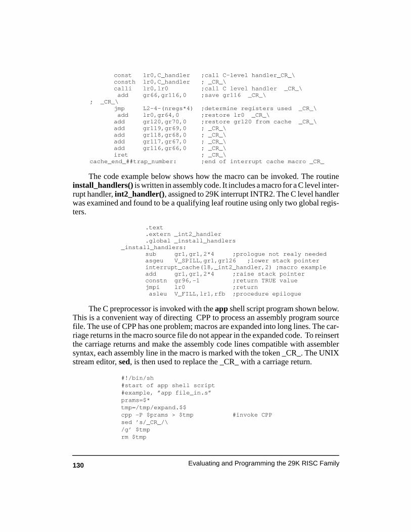
130 Evaluating and Programming the 29K RISC Family
const lr0,C_handler ;call C–level handler_CR_\consth lr0,C_handler ; _CR_\calli lr0,lr0 ;call C level handler _CR_\ add gr66,gr116,0 ;save gr116 _CR_\
; _CR_\jmp L2–4–(nregs*4) ;determine registers used _CR_\ add lr0,gr64,0 ;restore lr0 _CR_\add gr120,gr70,0 ;restore gr120 from cache _CR_\add gr119,gr69,0 ; _CR_\add gr118,gr68,0 ; _CR_\add gr117,gr67,0 ; _CR_\add gr116,gr66,0 ; _CR_\iret ; _CR_\
cache_end_##trap_number: ;end of interrupt cache macro _CR_
The code example below shows how the macro can be invoked. The routineinstall_handlers() is written in assembly code. It includes a macro for a C level inter-rupt handler, int2_handler(), assigned to 29K interrupt INTR2. The C level handlerwas examined and found to be a qualifying leaf routine using only two global regis-ters.
.text
.extern _int2_handler
.global _install_handlers_install_handlers:
sub gr1,gr1,2*4 ;prologue not realy neededasgeu V_SPILL,gr1,gr126 ;lower stack pointerinterrupt_cache(18,_int2_handler,2) ;macro exampleadd gr1,gr1,2*4 ;raise stack pointerconstn gr96,–1 ;return TRUE valuejmpi lr0 ;return asleu V_FILL,lr1,rfb ;procedure epilogue
The C preprocessor is invoked with the app shell script program shown below.This is a convenient way of directing CPP to process an assembly program sourcefile. The use of CPP has one problem; macros are expanded into long lines. The car-riage returns in the macro source file do not appear in the expanded code. To reinsertthe carriage returns and make the assembly code lines compatible with assemblersyntax, each assembly line in the macro is marked with the token _CR_. The UNIXstream editor, sed, is then used to replace the _CR_ with a carriage return.
#!/bin/sh#start of app shell script#example, ”app file_in.s”prams=$*tmp=/tmp/expand.$$cpp –P $prams > $tmp #invoke CPPsed ’s/_CR_/\ /g’ $tmp rm $tmp

131Chapter 2 Applications Programming
2.5.3 Using Signals to Deal with Interrupts
Some C language interrupt handlers will not be able to run in Freeze mode.; be-cause (as described in section 2.5) they are unsuitable leaf routines, or are not leafroutines and thus require use of the register stack. In this case the signal trampolinecode described in section 4.4 and Appendix B must be used. The trampoline code iscalled by the Freeze mode interrupt handler after critical registers have been saved onthe memory stack. The C language handler is called by the trampoline code after theregister stack is prepared for further use. Note that interrupts can occur at times whenthe register stack condition is not immediately usable by a C language handler.
The signal mechanism works by registering a signal handler function addressfor use when a particular signal number occurs. This is done with the library routinesignal(). Signals are normally generated by abnormal events and the signal() routineallows the operating system to call a user supplied routine which will be called to dealwith the event. The signal() function uses the signal HIF service to supply the addressof a library routine (sigcode) which will be called for all signals generated. (Note,only the signal, settrap and sigret–type subset of HIF services are required.) The li-brary routine is then responsible for calling the appropriate C handler from a table ofhandlers indexed by the signal number. When signal() is used a table entry isconstructed for the indicated signal.
signal(sig_number, func)int sig_number;void (*func)(sig_number);
A signal can only be generated for an interrupt if the code vectored to by the in-terrupt calls the shared library routine known as the trampoline code. It is known asthe trampoline code because signals bounce from this code to the registered signalhandler. To ensure that the trampoline code is called when an interrupt occurs, theFreeze mode code vectored to by the interrupt must pass execution to the trampolinecode, indicating the signal which has occurred. The signal_associate macro shownbelow can be used to install the Freeze Mode code and associate a signal number withthe interrupt or trap hardware number.
.reg it0,gr64;freeze mode interrupt
.reg it1,gr65;temporary registers
.macro signal_associate, trap_number, sig_number
sub gr1,gr1,4*4 ;get lr0–lr3 spaceasgeu V_SPILL,gr1,rab ;check for stack spilladd lr1,gr121,0 ;save gr121add lr0,gr96,0 ;save gr96const gr121,290 ;HIF 2.0 SETTRAP serviceconst lr2,trap_number ;trap number, macro parameterconst lr3,$1 ;trap handler address
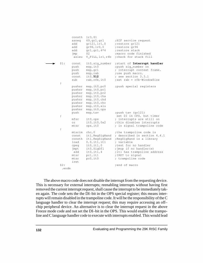
132 Evaluating and Programming the 29K RISC Family
consth lr3,$1asneq 69,gr1,gr1 ;HIF service requestadd gr121,lr1,0 ;restore gr121add gr96,lr0,0 ;restore gr96add gr1,gr1,4*4 ;restore stackjmp $2 ;macro code finished asleu V_FILL,lr1,rfb ;check for stack fill
$1: const it0,sig_number ;start of Interrupt handlerpush msp,it0 ;push sig_number onpush msp,gr1 ; interrupt context frame.push msp,rab ;use push macro,const it0, 512 ; see section 3.3.1sub rab,rfb,it0 ;set rab = rfb–WindowSize
;pushsr msp,it0,pc0 ;push special registerspushsr msp,it0,pc1pushsr msp,it0,pc2pushsr msp,it0,chapushsr msp,it0,chdpushsr msp,it0,chcpushsr msp,it0,alupushsr msp,it0,opspush msp,tav ;push tav (gr121)
; set DI in CPS, but timermfsr it0,ops ; interrupts are still onor it0,it0,0x2 ;this disables interruptsmtsr ops,it0 ; in signal trampoline code
;mtsrim chc,0 ;the trampoline code isconst it1,RegSigHand ; described in section 4.4.1consth it1,RegSigHand ;RegSigHand is a libraryload 0,0,it1,it1 ; variablecpeq it0,it1,0 ;test for no handlerjmpt it0,SigDfl ;jmup if no handler(s) add it0,it1,4 ;it1 has trampoline addressmtsr pc1,it1 ;IRET to signalmtsr pc0,it0 ; trampoline codeiret
$2: ;end of macro .endm
The above macro code does not disable the interrupt from the requesting device.This is necessary for external interrupts; reenabling interrupts without having firstremoved the current interrupt request, shall cause the interrupt to be immediately tak-en again. The code sets the the DI–bit in the OPS special register; this means inter-rupts will remain disabled in the trampoline code. It will be the responsibility of the Clanguage handler to clear the interrupt request; this may require accessing an off–chip peripheral device. An alternative is to clear the interrupt request in the aboveFreeze mode code and not set the DI–bit in the OPS. This would enable the trampo-line and C language handler code to execute with interrupts enabled. This would lead
133Chapter 2 Applications Programming
to the possibility of nested signal events; however, the signal trampoline code is ableto deal with such complex events.
With the example signal_associate macro the trampoline code and the C han-dler run in the processor mode at the time the interrupt occurred. They can be forcedto run in Supervisor mode by setting the Supervisor mode bit (SM–bit) when OR–ingthe DI–bit in the OPS register. Supervisor mode may be required to enable accessingof the interrupting device when disabling the interrupt request. The address transla-tion bits (PA and PD) may also be set at this time to turn off virtual addressing duringinterrupt processing. To make these changes to the above example code, the value0x72 should be OR–ed with the OPS register rather than the 0x2 value shown.
As described in section 2.5, a C language macro can be used to access the assem-bly level macro instruction. When the High C 29K compiler is being used, the defini-tion of the C macro is shown below. Users of the GCC compiler should replace the_ASM() call with the equivalent asm() C language extension.
#define signal_associate(tap_number, sig_number) \/*int trap_number; \ int sig_number; */ \ _ASM(” signal_associate ”#trap_number”,”#sig_number);
When the macro is used to associate a signal number with a processor trap num-ber, it is also necessary to supply the address of the C language signal handler calledwhen the signal occurs. The following example associates trap number 18 (floating–point exception) with signal number 8. This signal is known to UNIX and HIF usersas SIGFPE; when it occurs, the C handler sigfpe_handler is called.
_ASM(” .include \”interrupt_macros.h\””);signal_associate(18,8); /* trap 18, F–P */signal(8,sigfpe_handler); /* signal 8 handler */‘
C language signal handlers are free of many of the restrictions which apply toFreeze mode interrupt handlers. However, the HIF specification still restricts theiroperation to some extent. Signal handlers can only use HIF services with servicenumbers greater than 256. This means that printf() cannot be used. The reason forthis is HIF services below 256 are not reentrant, and a signal may occur while justsuch a HIF service request was being processed. Return from the signal handler mustbe via one of the signal return services: sigdft, sigret, sigrep or sigskp. If the signalhandler simply returns, the trampoline code will issue a sigdfl service request on be-half of the signal handler.
A single C level signal routine can be used to dispatch several C language inter-rupt handlers. Section 4.3.12 describes an interrupt queuing method, where interrupthandlers run in Freeze mode and build an interrupt descriptor (bead). Each descriptoris placed in a list (string of beads) and a Dispatcher routine is used to process descrip-tors. The signal handling method described above can be used to register a C level

134 Evaluating and Programming the 29K RISC Family
Dispatcher routine. This results in C level context being prepared only once and theDispatcher routine calling the appropriate C handler.
2.5.4 Interrupt Tag Words
Release 3.2, or newer, of the High C 29K compiler supports routines of definedreturn–type _Interrupt. The use of this C language extension causes an additional tagword to be placed ahead of the procedure code. Section 3.6 explains the format of theinterrupt tag in detail. Note, to use the _Interrupt key word with a PC hosted compiler,it is necessary to add the line “#define _Interrupt _CC(_INTERRUPT)” to file29k/bin/hc29.pro. The interrupt key word in conjunction with some simple supportroutines presented below make optimizing of interrupt preparation very easy. Byexamining the interrupt tag word it is possible to determine if a handler routinequalifies for Freeze mode execution or will require HIF signal processing. Theexample code shown below is for a HIF conforming operating system. However, adifferent operating system may choose to respond to interrupt tag information in asomewhat different manner. Only the signal, settrap and sigret–type subset of HIFservices are required. A different operating system may have equivalent supportservices.
When an interrupt occurs, it would be possible to examine the interrupt tag wordof the assigned handler. However, this would be an overhead encountered at eachinterrupt and it would increase interrupt processing time. It is better to examine thetag word at interrupt installation time and determine the necessary interruptpreparation code. Preceding sections have described interrupt context caching andsignal processing. It would be possible to examine the tag word in more detail thanthe following example code undertakes. This would produce additional intermediateperformance points in the spectrum of interrupt preparation code; context cachingbeing the fastest point on the spectrum and signal processing the slowest. However,signal processing can always be used and is free of the restrictions which apply to theuse of interrupt context caching, and context caching is frequently adequate. Thisrenders the chosen spectrum points as most practicable.
The example below shows two C language interrupt handler routines. The first,f_handler(), looks like it will qualify for Freeze mode execution. The key word_Interrupt has been used during the procedure definition and this will result in ainterrupt tag word. The second function, s_handler(), is not a leaf procedure and thisfact will be reported in its interrupt tag word. Being a non leaf routine, it will beprocessed as a signal handler. Such routines receive a single parameter –– the signalnumber.
extern int sig_sig /* defined in library code */extern int sig_intr0 /* signal for INTR0 */extern char *UART_p; /* pointer to UART */

135Chapter 2 Applications Programming
char recv_data[50];
_Interrupt f_handler() /* Freeze mode handler */{
static int count=0;recv_data[count]=*uart_p; /* read from UART */
if(recv_data[count]==’\n’) /* test for end */{ sig_sig=sig_intr0; /* signal #30 */
count=0; /* reset counter */}else count++;
}
_Interrupt s_handler(sig_number) /* signal handler */int sig_number; /* for sig_intr0 */{
printf(”in signal handler number=%d\n”, sig_number);printf(”received string=%s\n”, recv_data);_sigret();
}
Most programmers do not want to become concerned with the details ofinterrupt preparation. They simply wish to call an operating system service routinewhich will examine the interrupt tag word and select the appropriate interruptpreparation code. The library procedure, interrupt() , shown below, is just such aservice routine. The operation of this procedure will be described a little later. Theprocedure ensures that either interrupt context caching or signal processing will beapplied for the supplied handler and selected 29K trap number. The interrupt()routine must be executed during the system initialization stage, before traps orinterrupts are expected to occur. An example initialization sequence is shown below:
int sig_intr0;main(){
. . .sig_intr0=interrupt(16,s_handler); /* INTR0 */interrupt(17,f_handler); /* INTR1 */. . .
Interrupt tag words are dealt with at interrupt installation time, and not atprogram assembly or link time. There have been discussions about adding a compilerpragma option to High C 29K release 4.0 which, when switched on, will cause amacro instruction to be placed in output assembly code rather than an interrupt tagword. This requires that the relevant C code be compiled, then assembled with aninclude file which defines the replacement code for the interrupt macro instruction.This technique has some disadvantages, principally that the macro must understandthe capabilities of the operating system and how it intends dealing with interrupts. In

136 Evaluating and Programming the 29K RISC Family
particular; if the interrupt should be processed in User or Supervisor mode, withinterrupts enabled or disabled; with or without address translation and so on. Use of amacro does have the advantage that the interrupt preparation code appears in the finallinked program image. The tag word methods relies on the preparation code beingbuilt in heap memory during interrupt installation. The preparation code is built inconsultation with the operating system and is thus more portable between differentoperating systems which support somewhat different interrupt processingenvironments.
Fortunately for the user, library routines are responsible for installing theexecutable code into heap memory. The code itself is similar to the code of previoussections. A portion of the code is linked into text space of the program image. Atinstallation time the code is copied into heap memory and further optimized. Thecode sequence below is used for interrupt context caching.
.text
.align 4
.global _interrupt_cache_code
.global _interrupt_cache_end
.extern _sig_sig_interrupt_cache_code:
add gr80,gr111,0 ;save gr111 to interruptadd gr79,gr110,0 ; context cacheadd gr78,gr109,0add gr77,gr108,0add gr76,gr107,0add gr75,gr106,0add gr74,gr105,0add gr73,gr104,0add gr72,gr103,0add gr71,gr102,0add gr70,gr101,0add gr69,gr100,0add gr68,gr99,0add gr67,gr98,0add gr66,gr97,0add gr64,lr0,0 ;save lr0
;const lr0,0 ;const and consthconsth lr0,0 ; need to be modifiedcalli lr0,lr0 ;call C handler add gr65,gr96,0
;add gr111,gr80,0 ;restore gr111 fromadd gr110,gr79,0 ; context cacheadd gr109,gr78,0add gr108,gr77,0add gr107,gr76,0add gr106,gr75,0add gr105,gr74,0add gr104,gr73,0add gr103,gr72,0

137Chapter 2 Applications Programming
add gr102,gr71,0add gr101,gr70,0add gr100,gr69,0add gr99,gr68,0add gr98,gr67,0add gr97,gr66,0add gr96,gr65,0add lr0,gr64,0 ;restore lr0const gr64,_sig_sig ;the following eight consth gr64,_sig_sig ; instructions deal with load 0,0,gr64,gr64 ; sig_sig testingcpeq gr65,gr64,0 ;test for zeroconst gr66,_signal_associate_code + 4 ;no relativeconsth gr66,_signal_associate_code + 4 ; addressingjmpfi gr65,gr66 ;jump if sig_sig != 0 nopiret
_interrupt_cache_end:
The context cache code is a little different from the code shown in section 2.5.1.Eight extra instruction have been added to support a memory variable called sig_sig.It supports a very useful technique of two–level interrupt processing. Predominantlya Freeze mode interrupt handler is used alone. However, when the sig_sig variable isset to a signal number before the Freeze mode handler completes, a signal isgenerated causing a second signal handler routine to execute after the Freeze modehandler returns.
Examine the example handler routines. When interrupt INTR1 (vector 17)occurs, the Freeze mode handler, f_handler(), normally accesses the interruptingUART and receives a character; it then increments the count value and returns. Theprocesses of accessing the UART causes the interrupt request to be deasserted. Thisresults in a very fast interrupt handler written in C. However, when the receivedcharacter is a ‘\n’ (carriage return), sig_sig is set to the signal number allocated to theINTR0 signal handler. This causes the s_handler() to be executed in response to thesignal. The occurrence of interrupt INTR0 (vector 16) also causes s_handler() toexecute as a signal handler associated with trap 16. The example interrupt() serviceautomatically allocates signal numbers, starting with SIGUSR1, to handler routineswhich are to be processed via signal trampoline code. The interrupt() procedurereturns the selected signal number; zero is returned if a Freeze mode handler isselected. An interrupt handler can be restricted to fast Freeze mode processing andwhen more extensive processing is required the sig_sig variable can be set and asecond level handler invoked. (Note, the s_handler() routine calls the printf()library routine. This is not permitted with the High C 29K library routines as theprintf() routine is not reentrant. However, the use of printf() helps illustrate thetwo–stage principle.)
To perform signal processing, the trampoline code shown below is placed inheap memory. It is similar to the code of section 2.5.3. Interrupts are disabled before
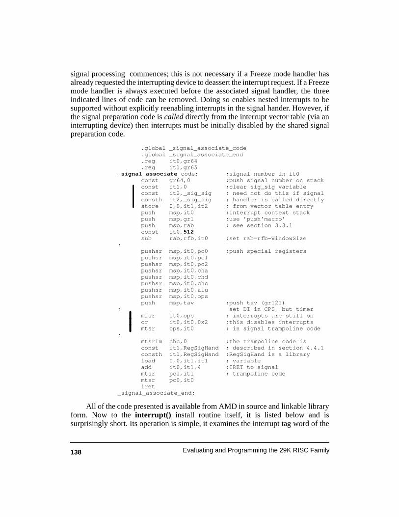
138 Evaluating and Programming the 29K RISC Family
signal processing commences; this is not necessary if a Freeze mode handler hasalready requested the interrupting device to deassert the interrupt request. If a Freezemode handler is always executed before the associated signal handler, the threeindicated lines of code can be removed. Doing so enables nested interrupts to besupported without explicitly reenabling interrupts in the signal hander. However, ifthe signal preparation code is called directly from the interrupt vector table (via aninterrupting device) then interrupts must be initially disabled by the shared signalpreparation code.
.global _signal_associate_code
.global _signal_associate_end
.reg it0,gr64
.reg it1,gr65_signal_associate _code: ;signal number in it0
const gr64,0 ;push signal number on stackconst it1,0 ;clear sig_sig variableconst it2,_sig_sig ; need not do this if signalconsth it2,_sig_sig ; handler is called directlystore 0,0,it1,it2 ; from vector table entrypush msp,it0 ;interrupt context stackpush msp,gr1 ;use ’push’macro’push msp,rab ; see section 3.3.1const it0, 512sub rab,rfb,it0 ;set rab=rfb–WindowSize
;pushsr msp,it0,pc0 ;push special registerspushsr msp,it0,pc1pushsr msp,it0,pc2pushsr msp,it0,chapushsr msp,it0,chdpushsr msp,it0,chcpushsr msp,it0,alupushsr msp,it0,opspush msp,tav ;push tav (gr121)
; set DI in CPS, but timermfsr it0,ops ; interrupts are still onor it0,it0,0x2 ;this disables interruptsmtsr ops,it0 ; in signal trampoline code
;mtsrim chc,0 ;the trampoline code isconst it1,RegSigHand ; described in section 4.4.1consth it1,RegSigHand ;RegSigHand is a libraryload 0,0,it1,it1 ; variableadd it0,it1,4 ;IRET to signalmtsr pc1,it1 ; trampoline codemtsr pc0,it0iret
_signal_associate_end:
All of the code presented is available from AMD in source and linkable libraryform. Now to the interrupt() install routine itself, it is listed below and issurprisingly short. Its operation is simple, it examines the interrupt tag word of the
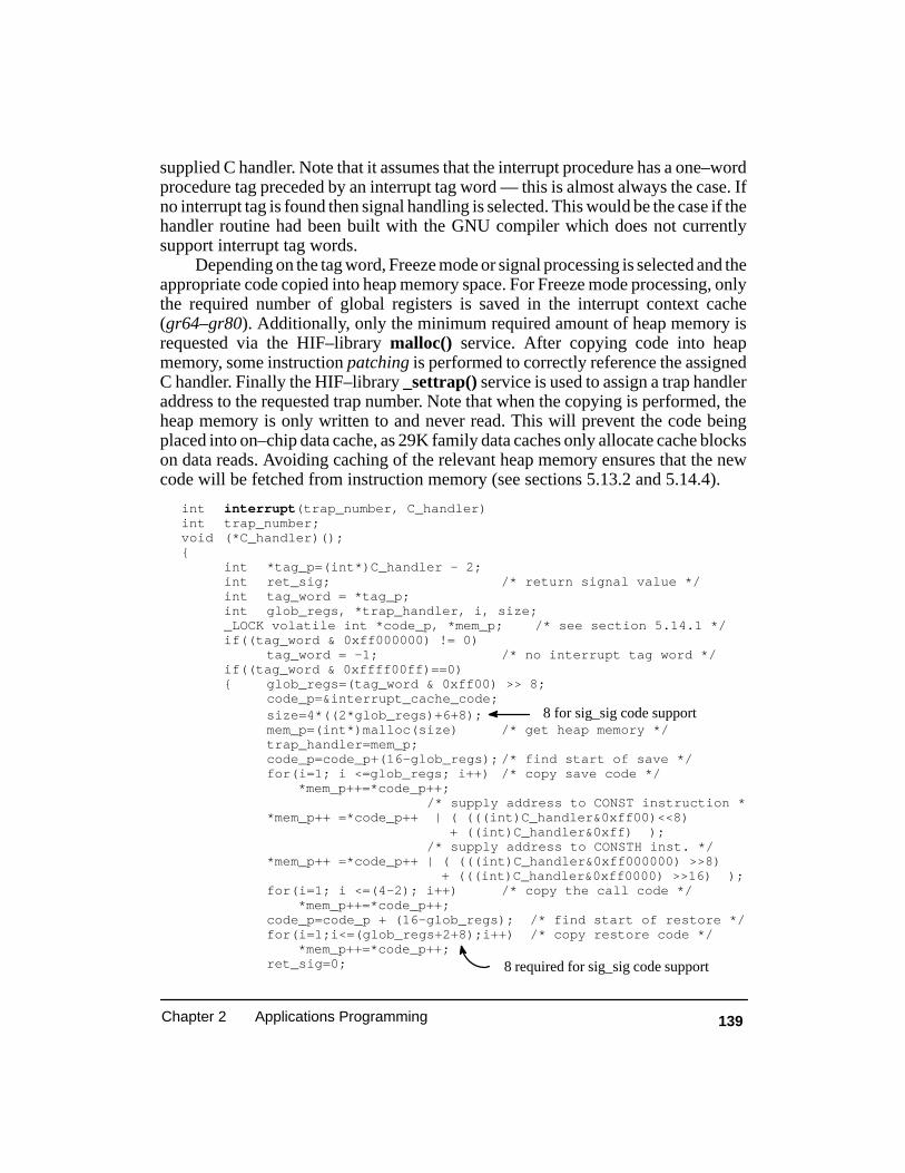
139Chapter 2 Applications Programming
supplied C handler. Note that it assumes that the interrupt procedure has a one–wordprocedure tag preceded by an interrupt tag word –– this is almost always the case. Ifno interrupt tag is found then signal handling is selected. This would be the case if thehandler routine had been built with the GNU compiler which does not currentlysupport interrupt tag words.
Depending on the tag word, Freeze mode or signal processing is selected and theappropriate code copied into heap memory space. For Freeze mode processing, onlythe required number of global registers is saved in the interrupt context cache(gr64–gr80). Additionally, only the minimum required amount of heap memory isrequested via the HIF–library malloc() service. After copying code into heapmemory, some instruction patching is performed to correctly reference the assignedC handler. Finally the HIF–library _settrap() service is used to assign a trap handleraddress to the requested trap number. Note that when the copying is performed, theheap memory is only written to and never read. This will prevent the code beingplaced into on–chip data cache, as 29K family data caches only allocate cache blockson data reads. Avoiding caching of the relevant heap memory ensures that the newcode will be fetched from instruction memory (see sections 5.13.2 and 5.14.4).
int interrupt (trap_number, C_handler)int trap_number;void (*C_handler)();{
int *tag_p=(int*)C_handler – 2;int ret_sig; /* return signal value */int tag_word = *tag_p;int glob_regs, *trap_handler, i, size;_LOCK volatile int *code_p, *mem_p; /* see section 5.14.1 */if((tag_word & 0xff000000) != 0)
tag_word = –1; /* no interrupt tag word */if((tag_word & 0xffff00ff)==0){ glob_regs=(tag_word & 0xff00) >> 8;
code_p=&interrupt_cache_code;size=4*((2*glob_regs)+6+8); 8 for sig_sig code supportmem_p=(int*)malloc(size) /* get heap memory */trap_handler=mem_p;code_p=code_p+(16–glob_regs); /* find start of save */for(i=1; i <=glob_regs; i++) /* copy save code */ *mem_p++=*code_p++;
/* supply address to CONST instruction **mem_p++ =*code_p++ | ( (((int)C_handler&0xff00)<<8) + ((int)C_handler&0xff) );
/* supply address to CONSTH inst. */*mem_p++ =*code_p++ | ( (((int)C_handler&0xff000000) >>8) + (((int)C_handler&0xff0000) >>16) );for(i=1; i <=(4–2); i++) /* copy the call code */ *mem_p++=*code_p++;code_p=code_p + (16–glob_regs); /* find start of restore */for(i=1;i<=(glob_regs+2+8);i++) /* copy restore code */ *mem_p++=*code_p++;
8 required for sig_sig code supportret_sig=0;

140 Evaluating and Programming the 29K RISC Family
}else{static int sig_number= 30 ; /* SIGUSR1 in SigEntry */
ret_sig=sig_number;signal(sig_number,C_handler);size=4*(signal_associate_end–signal_associate_code);mem_p=(int*)malloc(size); /* get heap memory */trap_handler=mem_p;code_p=signal_associate_code; /* supply sig_number to CONST instruction */*mem_p++ = *code_p++ | ( ((sig_number&0xff00)<<8)
+ (sig_number&0xff) );for(i=1; i <=(size–1); i++) /* copy rest of code */ *mem_p++ = *code_p++;sig_number++;
}_settrap(trap_number,(void(*)())trap_handler); /* HIF service */return ret_sig;
}
Users of the above code which do not want to make use of the two–levelinterrupt processing supported via the sig_sig variable, can remove the extra eightinstructions in the interrupt_cache_code and should also remove the extra codecopying indicated in the listing above. This will slightly improve interruptprocessing times for Freeze mode handlers. Other users who want to further exploitthe two–level approach can assign a single handler for all second level interruptprocessing, this is discussed in section 4.3.12. Interrupts are first dealt with in Freezemode by building an interrupt descriptor bead; then a second level Dispatcher routineis responsible for popping beads off a string and calling the assigned second levelhandler. Alternatively, a signal dispatcher technique can be applied; section 2.5.6describes the method. Signal dispatching can be achieved entirely with supportroutines accessible from C level –– this makes signal dispatching particularlyattractive.
If the interrupt() routine is used extensively for multiple signal handlers, it willbe necessary to increase the size of the signal handler array (SigEntry, described inAppendix B). The array is normally large enough to hold signal numbers 1 through32). Unless signal allocation is started at a number less than SIGUSR1 (30), there isnormally only sufficient space for two signal handlers.
2.5.5 Overloaded INTR3
The microcontroller members of the 29K family contain several on–chip pe-ripherals. These peripherals can generate interrupts which are all directed to the core29K processor via interrupt line INTR3. This causes overloading of the INTR3 vec-tor handler. When a microcontroller receives an INTR3 interrupt, it must examine itsInterrupt Control Register (ICR) to determine the source of the interrupt. This re-

141Chapter 2 Applications Programming
quires all interrupts to initially be processed via the INTR3 vector handler. TheINTR3 handler must call the appropriate device service routine. The service routinefirst clears the interrupt request by writing a one to the correct bit in the ICR; it canthen reenable interrupts and service the current request. The general format of theICR is shown on Figure 2-3.
07152331
IOPI
res
Figure 2-3. 29K Microcontroller Interrupt Control Register
Processor Specificreserved
VDI
res
DMA0I
8915
vector 220 224 228 237
The overloading of INTR3 adds complexity to the task of building a Freezemode interrupt handler for each interrupting device. The problem can be resolved byallocating a region of the vector table for use by the interrupting devices sharingINTR3. The code below (intr3 ) reserves 33 vector table entries starting with vector220 –– these vectors are not normally used by a 29K based system. When an INTR3occurs, the code examines the ICR register with a Count Leading Zeros (CLZ)instruction. This assigns the highest priority to the bit (interrupt) which is most–leftin the ICR register. The value produced by the CLZ instruction is added to the basevalue of 220 and the result used to obtain the correct vector entry from the vectortable.
.reg it0,gr64
.reg it1,gr65
.global _intr3_intr3 :
const it0,0x80000028 ;Interrupt Control register addressconsth it0,0x80000028load 0,0,it1,it0clz it1,it1 ;priority order index
;const it0, 220 ;base vector numberadd it1,it0,it1 ;add offset to basesll it1,it1,2 ;convert to word offsetmfsr it0,vab ;get vector table baseadd it1,it0,it1 ;get handler addressload 0,0,it1,it1 ; from vector table
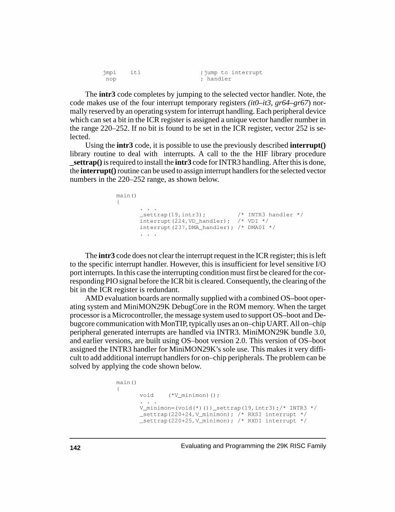
142 Evaluating and Programming the 29K RISC Family
jmpi it1 ;jump to interrupt nop ; handler
The intr3 code completes by jumping to the selected vector handler. Note, thecode makes use of the four interrupt temporary registers (it0–it3, gr64–gr67) nor-mally reserved by an operating system for interrupt handling. Each peripheral devicewhich can set a bit in the ICR register is assigned a unique vector handler number inthe range 220–252. If no bit is found to be set in the ICR register, vector 252 is se-lected.
Using the intr3 code, it is possible to use the previously described interrupt()library routine to deal with interrupts. A call to the the HIF library procedure_settrap() is required to install the intr3 code for INTR3 handling. After this is done,the interrupt() routine can be used to assign interrupt handlers for the selected vectornumbers in the 220–252 range, as shown below.
main(){
. . ._settrap(19,intr3); /* INTR3 handler */interrupt(224,VD_handler); /* VDI */interrupt(237,DMA_handler); /* DMA0I */. . .
The intr3 code does not clear the interrupt request in the ICR register; this is leftto the specific interrupt handler. However, this is insufficient for level sensitive I/Oport interrupts. In this case the interrupting condition must first be cleared for the cor-responding PIO signal before the ICR bit is cleared. Consequently, the clearing of thebit in the ICR register is redundant.
AMD evaluation boards are normally supplied with a combined OS–boot oper-ating system and MiniMON29K DebugCore in the ROM memory. When the targetprocessor is a Microcontroller, the message system used to support OS–boot and De-bugcore communication with MonTIP, typically uses an on–chip UART. All on–chipperipheral generated interrupts are handled via INTR3. MiniMON29K bundle 3.0,and earlier versions, are built using OS–boot version 2.0. This version of OS–bootassigned the INTR3 handler for MiniMON29K’s sole use. This makes it very diffi-cult to add additional interrupt handlers for on–chip peripherals. The problem can besolved by applying the code shown below.
main(){
void (*V_minimon)();. . .V_minimon=(void(*)())_settrap(19,intr3);/* INTR3 */_settrap(220+24,V_minimon); /* RXSI interrupt */_settrap(220+25,V_minimon); /* RXDI interrupt */
143Chapter 2 Applications Programming
_settrap(220+26,V_minimon); /* TXDI interrupt */. . .
The _settrap() HIF library service is used to install a new INTR3 handler; theaddress of the old handler is returned. The MiniMON29K code is used to processthree peripheral interrupts via INTR3. The _settrap() service is used again to sepa-rately reinstall the handlers required by MiniMON29K. New interrupt handlers foradditional on–chip peripherals can then be installed with further calls to _settrap() orinterrupt() .
2.5.6 A Signal Dispatcher
Release 3.2, or newer, of the High C 29K compiler supports routines of definedreturn–type _Interrupt. The use of this non–standard keyword was explained in sec-tion 2.5.4. The keyword is used here to support a signal dispatcher. The method relieson interrupts being processed in two stages. The first stage operates in Freeze mode.It responds immediately to the interrupting device, captures any critical data anddeactivates the interrupt request. The second stage, if required, takes the form of asignal handler. The sig_sig variable is used by the Freeze mode handler to requestsignal handler execution. A signal handler can not be executed without a freeze modehandler making the necessary request. This is because interrupts are not disabled inthe signal associate code.
The technique has a number of benefits: It is seldom necessary to disable inter-rupts for long periods, as asynchronous interrupt events are only initially dealt with inFreeze mode. This reduces interrupt latency. Signal handlers can be queued for pro-cessing when nested interrupts would occur. This eliminates the need to prepare a Clevel interrupt processing environment for each interrupt. A C level environmentneed only be built for a Signal Dispatcher routine. The Signal Dispatcher is then re-sponsible for calling the appropriate signal handler for all signals generated by inter-rupts. The Signal Dispatcher is started in response to the first signal occurring. Thedispatcher causes execution of the first signal handler, then determines if other signalhandlers have been requested while the current signal handler was executing. Thedispatcher continues to processes signals until there are none remaining. At this pointthe original interrupted state is restored. The original state being the processor state atthe time the first interrupt in the sequence occurred. The first interrupt occurred whileno interrupt or signal handler was being processed; and it caused the Signal Dispatch-er to start execution.
Avoiding nested interrupts, other than for Freeze mode handling, is mostbeneficial when large numbers of multiply nested interrupts are expected, and thecost of preparing C level context for interrupt processing is high. For example, usinginterrupt context caching, the processor can be prepared for Freeze mode interrupt
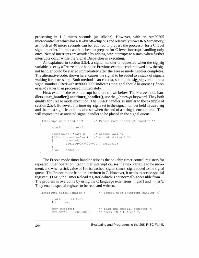
144 Evaluating and Programming the 29K RISC Family
processing in 1–2 micro seconds (at 16Mhz). However, with an Am29205microcontroller which has a 16–bit off–chip bus and relatively slow DRAM memory,as much as 40 micro seconds can be required to prepare the processor for a C levelsignal handler. In this case it is best to prepare for C level interrupt handling onlyonce. Nested interrupts are avoided by adding new interrupts to a stack when furtherinterrupts occur while the Signal Dispatcher is executing.
As explained in section 2.5.4, a signal handler is requested when the sig_sigvariable is set by a Freeze mode handler. Previous example code showed how the sig-nal handler could be started immediately after the Freeze mode handler completes.The alternative code, shown here, causes the signal to be added to a stack of signalswaiting for processing. Both methods can coexist, setting the sig_sig variable to asignal number ORed with 0x8000,0000 indicates the signal should be queued (if nec-essary) rather than processed immediately.
First, examine the two interrupt handlers shown below. The Freeze mode han-dlers, uart_handler() and timer_handler(), use the _Interrupt keyword. They bothqualify for Freeze mode execution. The UART handler, is similar to the example ofsection 2.5.4. However, this time sig_sig is set to the signal number held in uart_sigand the most significant bit is also set when the end of a string is encountered. Thiswill request the associated signal handler to be placed in the signal queue.
_Interrupt uart_handler() /* Freeze mode interrupt handler */{
static int count=0;
recv[count]=*uart_p; /* access UART */if(recv[count]==’\n’) /* end of string ? */{ count=0;
sig_sig=0x80000000 | uart_sig;}else count++;
}
The Freeze mode timer handler reloads the on–chip timer control registers forrepeated timer operation. Each timer interrupt causes the tick variable to be incre-ment, and when a tick value of 100 is reached, signal timer_sig is added to the signalqueue. The Freeze mode handler is written in C. However, it needs to access specialregister 9 (TMR, the Timer Reload register) which is not normally accessible from C.The problem is overcome by using the C language extensions _mfsr() and _mtsr().They enable special register to be read and written.
_Interrupt timer_handler() /* Freeze mode interrupt handler */{
static int tick=0;int tmr;
tmr=_mfsr(9); /* read TMR special register */tmr=tmr&(–1–0x02000000) /* clear IN bit–field */
145Chapter 2 Applications Programming
_mtsr(9,tmr); /* write to TMR register */if(tick++ > 100){ tick=0;
sig_sig=0x80000000 | timer_sig;}
}
The second stage of the UART interrupt handler, the signal handler, is shownbelow. Note, the sig_uart() routine calls the printf() library routine. This is not per-mitted with the High C 29K library routines as the printf() routine is not reentrant.However, the use of printf() helps illustrate the operating principle. Normally a sig-nal handler must use the _sigret() signal return service, at least with a HIF conform-ing operating system. However, when a signal handler is called from the dispatcher,the signal return service should not be used. It is possible to determine if the dispatch-er is in use by testing the variable dispatcher_running; it becomes non zero whenthe dispatcher is in use. However, testing the dispatcher_running flag may be insuf-ficient in some circumstances. It is possible that the Signal Dispatcher is running andinitiating signal handler execution. At the same time a signal handler may be re-quested directly by, say, an interrupt. The Dispatcher is running but the directly re-quested signal handler must use the signal return service.
Signals need not always be queued for processing. If a very high priority (im-mediate) interrupt occurs and further signal processing is necessary, sig_sig shouldbe simply set to the signal number. In this case it is important that the signal handleruse the _sigret() service.
_Interrupt sig_uart(sig_number) /* signal handler for UART */int sig_number;{
printf(”in signal handler number=%d\n”, sig_number);printf(”received string=%s\n”, recv_data);if(!dispatcher_running)_sigret(); /* no _sigret() service call *
}
The Signal Dispatcher is implemented as a signal handler. The dispatcher re-moves signals from a stack and calls the appropriate signal handler. When a signalhandler is requested by a Freeze mode handler, and the Signal Dispatcher is not cur-rently executing, the requested signal (sig_sig value) is not immediately started. In itsplace the dispatcher signal handler is initiated.
Shown on Figure 2-4 is an example of the Signal Dispatcher in operation. Thefirst interrupt is from the UART. It is dealt with entirely in Freeze mode; the sig_sigvariable is not set such as to request a second stage signal handler. The UART gener-ates the second interrupt. This time the sig_sig variable is set to request the sig_uart()signal handler be started by the Signal Dispatcher. While the second stage handler isrunning, a timer interrupt occurs. The Freeze mode timer handler requests a secondstage handler be started by the Signal Dispatcher. When the dispatcher completes thecurrently executing second stage handler (the UART’s), it initiates the timer’s second

146 Evaluating and Programming the 29K RISC Family
Figure 2-4. Processing Interrupts with a Signal Dispatcher
Freeze mode codeuart_handler()sig_sig =0
sig_dispatcher()Signal Dispatcher
Pop uart_sig off stack
uart_handler()sig_sig=uart_sig|0x8..
signal_associate_codePush uart_sig on stack
“signal”=uart_sig
“signal”=dispatcher_sig
sig_uart()2nd stage signal
handler
call
Signal DispatcherPop timer_sig off stack
sig_timer()2nd stage signal
handler
call
timer_handler()sig_sig=timer_sig|0x8..
Signal Dispatchercall _sigret()
End
signal return service
Full C–context code
UARTinterrupt
timerinterrupt
signal_associate_codePush timer_sig on stack
“signal”=timer_sig
Main Program
Main Program
stage handler. When there are no remaining second stage handler requests, the dis-patcher issues a signal–return service request. The original programs context is thenrestored and its execution restarted.
Integer variable dispatcher_sig holds the signal number used by the SignalDispatcher. The user must select a signal number. The example code below uses 7(SIGEMT). The signal() library routine is used to assign procedure sig_dispatcher()to signal number 7. Before signal and trap handlers can be installed, the proceduresand variables defined in the support libraries must be declared external; as shownbelow.
extern void signal(int, void (*handler)(int));extern int interrupt(int, _Interrupt (*C_handler)(int));extern void sig_dispatcher(int);
147Chapter 2 Applications Programming
extern int sig_sig;extern int dispatcher_sig ; /* dispatcher signal number */
int uart_sig, timer_sig;
During program initialization, after main() is called, the handler routines andother support services must be installed. The code below uses the interrupt() libraryroutine to install a signal handler (sig_timer() not shown) for timer interrupt support.The call to interrupt() returns the allocated signal number, and this number is savedin timer_sig. The timer Freeze mode handler uses the timer_sig value to request thetimer signal handler be executed. The interrupt() service is called a second time toinstall the Freeze mode handler, timer_handler(). The second call causes vectortable entry 14 to be reassigned the address of the Freeze mode handler.
The UART handlers are installed using an alternative method. The signal() ser-vice rather than the interrupt() service is used to assign the sig_uart() signal handlerto signal number SIGUSR2. This method allows a specific signal number to be se-lected, rather than using the interrupt() service to allocate the next available signalnumber. Most users will prefer the previous method used to automatically select sig-nal numbers.
main(){
_settrap(218,_disable);_settrap(217,_enable);_settrap(216,_timer_init);
dispatcher_sig=7; /* select signal number for dispatcher */signal(dispatcher_sig, sig_dispatcher );
timer_sig=interrupt(14,sig_timer); /* install signal handler */if(interrupt(14,timer_handler)) /* install Freeze handler */ printf(”ERROR: Freeze mode handler not built for trap 14\n”);
if(interrupt(15,uart_handler) /* install Freeze handler */ printf(”ERROR: Freeze mode handler not built for trap 15\n”);uart_sig=SIGUSR2; /* chose a signal number */signal(uart_sig,sig_uart); /* install signal handler */
timer_init(); /* initialize the timer */. . .
The sig_dispatcher() requires two helper services, disable() and enable().They are described in more detail shortly, but are simply used to enable and disableprocessor interrupts. The _settrap() service is used above to install trap handlers forthese services. The timer_init() routine is not required by the Signal Dispatcher. It isincluded to simply make the example more complete.
The interrupt() routine uses the signal_associate method of assigning a trapnumber to a signal handler. The code was described in section 2.5.4, but a few small
148 Evaluating and Programming the 29K RISC Family
additions are required to support the Signal Dispatcher. The modified code is shownbelow. There are two changes: Interrupts are not disabled (requiring that a Freezemode handler always be used for interrupt deactivation). A call to queue_sig is madeif the most significant bit of the signal number is set.
.reg it0,gr64
.reg it1,gr65_signal_associate _code: ;signal number in it0
const gr64,0 ;push signal number on stack;
const it1,0 ;clear sig_sig variableconst it2,_sig_sig ; need not do this if signalconsth it2,_sig_sig ; handler is called directlystore 0,0,it1,it2 ; from vector table entry
;const it1, _queue_sigconsth it1, _queue_sigjmpti gr64,it1 ;jump if msb–bit set noppush msp,it0 ;interrupt context stackpush msp,gr1 ;use ’push’ macro’push msp,rab ; see section 3.3.1const it0, 512sub rab,rfb,it0 ;set rab=rfb–WindowSize
;pushsr msp,it0,pc0 ;push special registerspushsr msp,it0,pc1pushsr msp,it0,pc2pushsr msp,it0,chapushsr msp,it0,chdpushsr msp,it0,chcpushsr msp,it0,alupushsr msp,it0,opspush msp,tav ;push tav (gr121)
;mtsrim chc,0 ;the trampoline code isconst it1,RegSigHand ; described in section 4.4.1consth it1,RegSigHand ;RegSigHand is a libraryload 0,0,it1,it1 ; variableadd it0,it1,4 ;IRET to signalmtsr pc1,it1 ; trampoline codemtsr pc0,it0iret
_signal_associate_end:
The queue_sig routine is shown below. It pushes the signal number on a signalstack and advances a stack pointer, sig_stack_p. The operation is performed whilestill in Freeze mode and is therefor not interruptible. The variabledispatcher_running is then tested. If it is set to TRUE, an interrupt return (IRET)instruction is issued. If it is FALSE, the dispatcher_sig number is obtained and thesignal_associate code continues the process of starting a signal handler; but the

149Chapter 2 Applications Programming
signal number now in use will cause the Signal Dispatcher (sig_dispatcher()) tocommence execution.
_queue_sig : ;jump here from signal_associateand it0,it0,0xff ;clear msb–bit
;const it3,_sig_stack_pconsth it3,_sig_stack_pload 0,0,it2,it3 ;get pointer valuestore 0,0,it0,it2 ;store signal number on stackadd it2,it2,4 ;advance stack pointerstore 0,0,it2,it3
;const it3,_dispatcher_runningconsth it3,_dispatcher_runningload 0,0,it2,it3 ;test if signal dispatchercpeq it2,it2,0 ; already runningjmpt it2,_start_dispatcher constn it2,–1iret ;IRET if running
;_start_dispatcher:
store 0,0,it2,it3 ;set dispatcher_runningconst it3,_dispatcher_sigconsth it3,_dispatcher_sigconst it1,_signal_associate_code+5*4consth it1,_signal_associate_code+5*4jmpi it1 ;start signal handler load 0,0,it0,it3 ;signal=dispatcher_sig
Before the signal_associate code starts the dispatcher signal handler, thedispatcher_running variable is set to TRUE. Until this variable is cleared, furthersignal requests (if the most significant bit of the signal number is set) will be added tothe queue of signals waiting for processing. The process of adding a signal to thequeue is kept simple –– a stack is used. Reducing the amount of code required resultsin less interrupt latency as the queue_sig code runs in Freeze mode.
The signal handler which performs the dispatch operation is written in C. Thecode is shown below. It requires some simple assembly–level support routines whichare described later. Having the code in C is a convenience as it simplifies the task ofmodifying the code. Modification is necessary if a different execution schedule isrequired for signals waiting in the signal stack. The variables used in the SignalDispatcher routine are described below. Note, that sig_stack_p anddispatcher_running are defined volatile. This is because they may also be modifiedby a Freeze mode interrupt handler. It is important that the C compiler be informedabout this possibility. Otherwise it may perform optimizations which prevent valuechanges from being observed, such as holding a copy of sig_dispatcher_p inregister, and repeatedly accessing the register.

150 Evaluating and Programming the 29K RISC Family
extern void (*_SigEntry[])(int); /* defined in HIF libraries */
int sig_stack[200]; /* signal stack */volatile int *sig_stack_p=&sig_stack[0];volatile int dispatcher_running; /* dispatcher running flag */int sig_sig=0;int dispatcher_sig; /* dispatcher signal number */
The example sig_dispatcher() is relatively simple but effective. It first disablesinterrupts before removing all current signals from the stack. The signal values aretransferred to an array. Interrupts are then reenabled. Performing this procedure withinterrupts disabled prevents other signals being added to the stack while the transferoperation is being performed. Signals are transferred to the array in the reverse orderthey were placed on the stack. This ensures that signals are ultimately processed inthe order in which they were originally requested.
No attempt is made to apply a priority order to pending signals. The necessarycode can be applied after the signals have been removed from the stack. Performingpriority ordering at C–level rather than in the sig_queue code has the advantage ofreducing interrupt latency. Due to the fast operation of 29K processors the need topriority order signals is not high, as a signal request is not likely to be kept waitingvery long.
void sig_dispatcher (sig) /* Signal Dispatcher */int sig;{
int cps;int *sig_p; /* array of signals */static int sig_array[20]; /* needing processing */cps=disable(0x20002); /* set DI and TD in CPS */for(;;){ sig_p=&sig_array[0]; /* mark array empty */
while(sig_stack_p!=&sig_stack[0])/* remove signals from{ ––sig_stack_p; /* stack */
*sig_p++=*(int*)sig_stack_p; /* copy from } /* stack to array */enable(cps); /* enable interrupts */while(sig_p!=&sig_array[0]) /* process signals removed */{ ––sig_p; /* from stack */
(*_SigEntry[(*sig_p)–1])(*sig_p);}cps=disable(0x20002); /* disable interrupts */if(sig_stack_p==&sig_stack[0]) /* stack empty ? */
break;}dispatcher_running=0;enable(cps); /* enable interrupts */_sigret(); /* _sigret() HIF service */
} /* would restore interrupted cps */
When there are no remaining signals to process, the dispatcher requests the_sigret() signal–return service. The dispatcher_running flag is also cleared. It is

151Chapter 2 Applications Programming
possible that a new signal arrives just after the flag is cleared but before thesignal–return service is complete, this can not be avoided. It does not create aproblem (other than a loss of performance) as a new dispatcher signal handler issimply started.
The disable() and enable() support routines are used by the Signal Dispatcher toenable and disable interrupts around critical code. Interrupts are disabled by settingthe DI bit in the Current Processor Status (CPS) register. Freeze mode handler rou-tines can use the _mtsr() C language extensions to modify special registers. However,they can not be used by the dispatcher routine as it may be operating in User mode.Accessing special register space from User mode would create a protection violation.The problem is overcome by installing assembly level trap handlers which performthe necessary special register access. The _settrap() HIF service is used to install thetrap handlers. Further assembly routines are required to assert the selected trap num-ber. The code for disable() is shown below.
.global _disable_disable:
asneq 218,gr96,gr96jmpi lr0 nop
.global __disable__disable:
mfsr gr96,ops ;read OPSor gr97,gr96,lr2 ;OR with passed valuemtsr ops,gr97iret ;copy OPS to CPS
A single parameter is passed to disable(). The parameter is ORed with the CPSvalue and the CPS register updated. Since this task is performed by a trap handler, theOPS register is actually modified; and OPS is copied to CPS when an IRET is issued.There is a further advantage of using a trap handler to perform the task; the operationcan not be interrupted –– the read/modify/write of the the CPS is atomic.
The code for enable() is similar to disable(). In this case the passed parameter issimply copied to the CPS. The disable() routine returns the CPS value before modi-fying it. The value is normally stored and later passed to enable(). In this way only theDI and TD (timer disable) bits in the CPS are temporarily modified. Note, oldermembers of the 29K family do not support the TD bit. In such case, the interrupt dis-able code used by the example sig_dispatcher() routine does not prevent interruptsbeing generated by the on–chip timer. The the problem can be resolved by modifyingthe __enable and __disable assembly routines to clear and set the interrupt enable(IE) bit in the Timer Reload register.
.global _enable_enable:
asneq 217,gr96,gr96

152 Evaluating and Programming the 29K RISC Family
jmpi lr0 nop
.global __enable__enable:
mtsr ops,lr2iret
2.5.7 Minimizing Interrupt Latency
Interrupt latency is minimized if interrupts are never disabled. In practice thiscan be difficult to achieve. There are often critical code sections which must run tocompletion without interruption. Traditionally, interrupts are disabled before enter-ing such code sections and reenabled upon critical section completion. However, ifinterrupts are processed using the two–stage method described in section 2.5.6 (ASignal Dispatcher), interrupt disabling can be eliminated.
In place of disabling interrupts around a critical code section, the Signal Dis-patcher is effectively disabled. This allows a first stage interrupt handler to interrupt acritical code section. Second stage interrupt handlers (signal handlers) are not initi-ated during the critical code section, as the Dispatcher is disabled. It is easy to disablethe Dispatched by simply indicating that it is already active; this will prevent its ac-tivation which can occur when the first stage handler is completed (if the sig_sig vari-able is set). First stage handlers execute in Freeze mode and can be configured toavoid access to the shared resource being accessed by critical code sections. The ex-ample below shows how the Signal Dispatcher can be deactivated around a criticalcode section.
#define TRUE –1#define FALSE 0
. . . interruptible codedispatcher_running=TRUE; /* disable Dispatcher */. . . start of critical code section
/* code only interruptible by Freeze mode handler */
. . . end of critical code sectiondispatcher_running=FALSE; /* enable Dispatcher */if(sig_stack_p!=&sig_stack[0])
_sendsig(dispatcher_sig);. . .
When the critical task has been accomplished, the Dispatcher is reenabled byclearing the dispatcher_running variable. It is possible that one or more signal num-bers were pushed on the signal stack during the critical stage. Hence, when the Dis-patcher is reenabled, the signal stack must be tested to determine if there are anypending signals. If there are, then the Signal Dispatcher must be started using the_sendsig() HIF service.
153Chapter 2 Applications Programming
The method minimizes the latency in starting a Freeze mode interrupt handlersince their commencement is never disabled –– unless by another Freeze mode han-dler. The latency in starting a second stage handler is not reduced. Further restrictionsmay have to be applied to first stage handlers to disallow access to resources whichmust be atomically manipulated within critical code sections –– such as linked–listdata structures.
2.5.8 Signal Processing Without a HIF Operating System
A signal processing technique is recommended for dealing with complex C lev-el interrupt handlers. The previous sections have described in detail how signal pro-cessing can be performed. AMD and other tool providers supply the necessary sup-port code which has been well tested and is known to be reliable. However, some de-velopers may select an operating system which does not support the HIF services re-quired by the previous example code. Additionally, many embedded system are de-pendant on simple home–made boot–up code, which provides few support services.
A commercial operating system will implement its own interrupt processingservices. It is likely these services will be somewhat based on the signal processingcode described in this book. However, the provided services should be used in prefer-ence to the HIF services. In fact, the chosen operating system may not provide anysupport for HIF services.
When building simple boot–up and run–time support code for a smallembedded system, it is best to provide the necessary HIF services required for signalprocessing. If the boot–up code is based on AMD’s OS–boot product, then all HIFservices will be provided. If OS–boot is not used, it is important that limited HIFsupport be included in the developed code. Only the signal, settrap, sysalloc andsigret–type subset of HIF services are required. A trap handler for HIF trap number69 should be installed, and the code required to process the HIF service requestinstalled. Very little code is required and example code can be taken from OS–boot.
2.5.9 An Example Am29200 Interrupt Handler
The following example makes use of the code presented in the previous sectionsof this chapter. The Programmable I/O (PIO) port of an Am29200 microcontroller isconfigured such that PIO signal–pin PIO0 is an output, and PIO signal–pin PIO15 aninput. The system hardware ensures that the two pins are wired together. A two stageinterrupt handler is assigned to processing interrupts generated by a rising edge onpin PIO15. By first clearing pin PIO0 and then setting it to one, an interrupt will begenerated.
First, a number of include files must be accessed to declare external data andprocedure type information. Newer versions of file signal.h contain the externdeclarations listed below. Hence, only when using an older signal.h file need theextern statement be explicitly included.
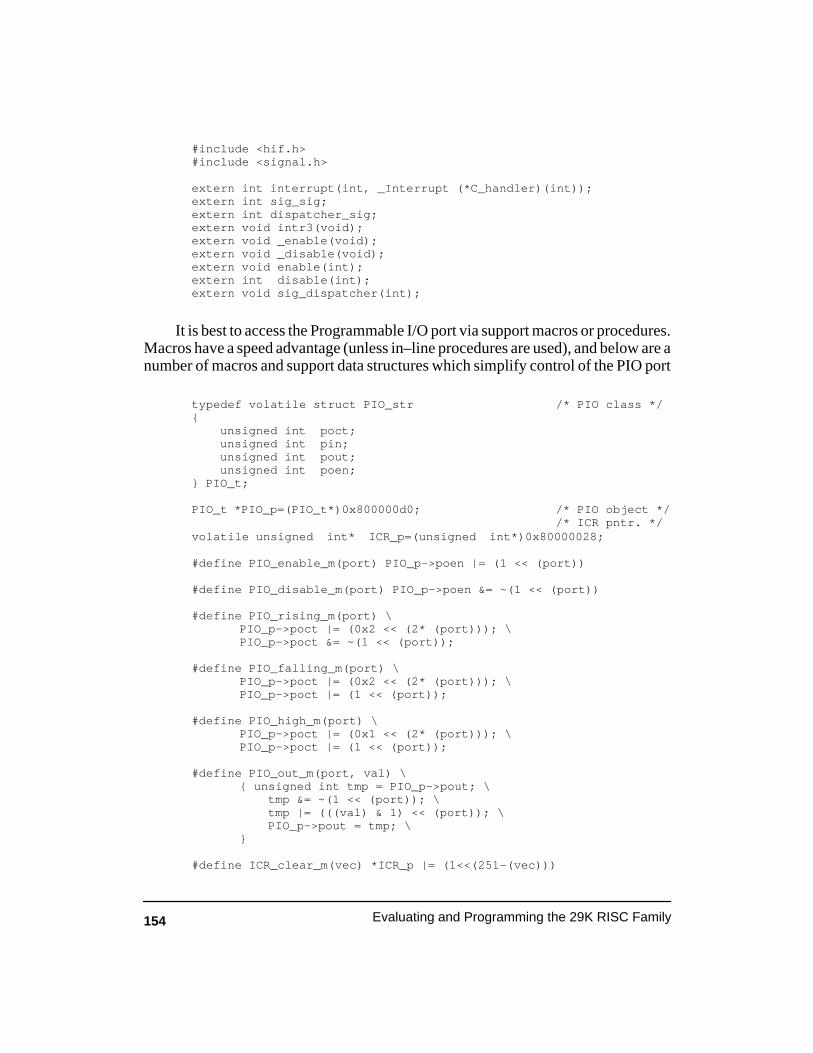
154 Evaluating and Programming the 29K RISC Family
#include <hif.h>#include <signal.h>
extern int interrupt(int, _Interrupt (*C_handler)(int));extern int sig_sig;extern int dispatcher_sig;extern void intr3(void);extern void _enable(void);extern void _disable(void);extern void enable(int);extern int disable(int);extern void sig_dispatcher(int);
It is best to access the Programmable I/O port via support macros or procedures.Macros have a speed advantage (unless in–line procedures are used), and below are anumber of macros and support data structures which simplify control of the PIO port
typedef volatile struct PIO_str /* PIO class */{ unsigned int poct; unsigned int pin; unsigned int pout; unsigned int poen;} PIO_t;
PIO_t *PIO_p=(PIO_t*)0x800000d0; /* PIO object *//* ICR pntr. */
volatile unsigned int* ICR_p=(unsigned int*)0x80000028;
#define PIO_enable_m(port) PIO_p–>poen |= (1 << (port))
#define PIO_disable_m(port) PIO_p–>poen &= ~(1 << (port))
#define PIO_rising_m(port) \PIO_p–>poct |= (0x2 << (2* (port))); \PIO_p–>poct &= ~(1 << (port));
#define PIO_falling_m(port) \PIO_p–>poct |= (0x2 << (2* (port))); \PIO_p–>poct |= (1 << (port));
#define PIO_high_m(port) \PIO_p–>poct |= (0x1 << (2* (port))); \PIO_p–>poct |= (1 << (port));
#define PIO_out_m(port, val) \{ unsigned int tmp = PIO_p–>pout; \ tmp &= ~(1 << (port)); \ tmp |= (((val) & 1) << (port)); \ PIO_p–>pout = tmp; \}
#define ICR_clear_m(vec) *ICR_p |= (1<<(251–(vec)))
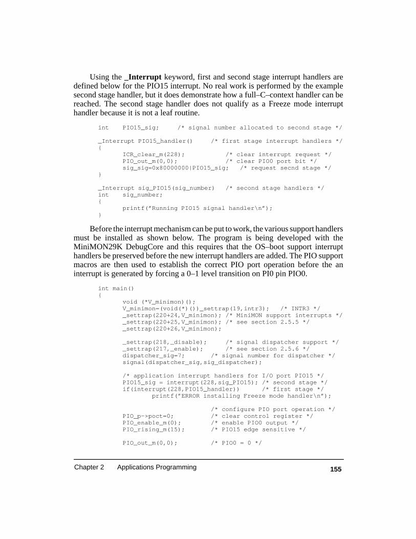
155Chapter 2 Applications Programming
Using the _Interrupt keyword, first and second stage interrupt handlers aredefined below for the PIO15 interrupt. No real work is performed by the examplesecond stage handler, but it does demonstrate how a full–C–context handler can bereached. The second stage handler does not qualify as a Freeze mode interrupthandler because it is not a leaf routine.
int PIO15_sig; /* signal number allocated to second stage */
_Interrupt PIO15_handler() /* first stage interrupt handlers */{
ICR_clear_m(228); /* clear interrupt request */PIO_out_m(0,0); /* clear PIO0 port bit */sig_sig=0x80000000|PIO15_sig; /* request secnd stage */
}
_Interrupt sig_PIO15(sig_number) /* second stage handlers */int sig_number;{
printf(”Running PIO15 signal handler\n”);}
Before the interrupt mechanism can be put to work, the various support handlersmust be installed as shown below. The program is being developed with theMiniMON29K DebugCore and this requires that the OS–boot support interrupthandlers be preserved before the new interrupt handlers are added. The PIO supportmacros are then used to establish the correct PIO port operation before the aninterrupt is generated by forcing a 0–1 level transition on PI0 pin PIO0.
int main(){
void (*V_minimon)();V_minimon=(void(*)())_settrap(19,intr3); /* INTR3 */_settrap(220+24,V_minimon); /* MiniMON support interrupts */_settrap(220+25,V_minimon); /* see section 2.5.5 */_settrap(220+26,V_minimon);
_settrap(218,_disable); /* signal dispatcher support */_settrap(217,_enable); /* see section 2.5.6 */dispatcher_sig=7; /* signal number for dispatcher */signal(dispatcher_sig,sig_dispatcher);
/* application interrupt handlers for I/O port PIO15 */PIO15_sig = interrupt(228,sig_PIO15); /* second stage */if(interrupt(228,PIO15_handler)) /* first stage */
printf(”ERROR installing Freeze mode handler\n”);
/* configure PIO port operation */PIO_p–>poct=0; /* clear control register */PIO_enable_m(0); /* enable PIO0 output */PIO_rising_m(15); /* PIO15 edge sensitive */
PIO_out_m(0,0); /* PIO0 = 0 */

156 Evaluating and Programming the 29K RISC Family
PIO_out_m(0,1); /* generate an interrupt */}
Users of the High C 29K tool chain could test the interrupt handling mechanismwithout first building the necessary hardware by asserting the assigned trap numberas shown below.
_ASM(” asneq 228,gr1,gr1”); /* test interrupt mechanism */
2.6 SUPPORT UTILITY PROGRAMS
There are a number of important utility programs available to the software de-veloper. These tools are generally available on all development platforms and areshared by different tool vendors. Most of the programs operate on object files pro-duced by the assembler or linker. All linkable object files and executable files aremaintained in AMD Common Object File Format (COFF). This standard is veryclosely based on the AT&T standard used with UNIX System V. Readers wishing toknow more about the details of the format may consult the High C 29K documenta-tion or the AT&T Programmer’s Guide for UNIX System V. The coff.h include filefound on most tool distributions, describes the C language data structures used by theCOFF standard –– often described as the COFF wrappers.
2.6.1 Examining Object Files (Type .o And a.Out)
nm29The nm29 utility program is used to examine the symbol table contained in abinary COFF file produced by the compiler, assembler or linker. The format isvery much like the UNIX nm utility. Originally nm29 was written to supplysymbol table information to the munch29 utility in support of the AT&T C++cfront program. A number of command line options have been added to enableadditional information to be printed, such as symbol type and section type.
One useful way to use nm29 is to pipe the output to the sort utility, for example:“nm29 a.out | sort | more”; each symbol is printed preceded by its value. The sortutility arranges for symbol table entries to be presented in ascending value.Since most symbols are associated with address labels, this is a useful way tolocate an address relative to its nearest address labels.
munch29This utility is used with the AT&T C++ preprocessor. This program is known ascfront and converts C++ programs into C. After the C++ program has beenconverted and linked with other modules and libraries, it is examined with

157Chapter 2 Applications Programming
nm29 to determine the names of any static constructor and destructor functions.The C++ translator builds these functions as necessary and tags their names withpredefined character sequences. The output from nm29 is passed to munch29which looks for constructor and destructor names. If found, munch29 builds Cprocedures which call all the identified object constructors and destructors.Because the constructor functions must execute before the application main()program, the original program is relinked with the constructor procedures beingcalled before main(). The main() entry is replaced with _main(). This alsoenables the call to destructor procedures to be made in _main() when main()returns.
Because G++ is now available for C++ code development (note, G++ isincorporated into the GCC compiler), there is little use being made of the AT&Tcfront preprocessor. Additionally, MRI and Metaware are expected to shortlyhave commercial C++ compilers available.
rdcoffThe rdcoff utility is only available to purchasers of the High C 29K product.This utility prints the contents of a COFF conforming object file. Each COFFfile section is presented in an appropriate format. For example, text sections aredisassembled. If the symbol table has not been striped from the COFF file, thensymbol values are shown. The utility is useful for examining COFF headerinformation, such as the text and data region start addresses. Those using GNUtools can use the coff and objdump utilities to obtain this information.
coff This utility is a shorthand way of examining COFF files. It reports a summary ofCOFF header information, followed by similar reports for each of the sectionsfound in the object file. The utility is useful for quickly checking the linkmapping of a.out type files; especially when a project is using a number ofdifferent 29K target systems which have different memory system layouts,requiring different program linkage.
objdumpThis utility is supplied with the GNU tool chain. It can be used to examineselected parts of object files. It has an array of command line options which arecompatible with the UNIX System V utility of the same name. In a similar wayto the rdcoff utility it attempts to format selected information in a meaningfulway.
swafThis utility is used to produce a General–Purpose ASCII (PGA) symbols file foruse with Hewlett–Packard’s B3740A Software Analyzer tool. This tool enablesa 16500B card cage along with a selection of logic analyzer cards to supporthigh level software debugging. The swaf utility builds a GPA symbols file from
158 Evaluating and Programming the 29K RISC Family
information extracted from a linked COFF file. When the GPA file is loaded intothe analyzer it is possible to display address values in symbol format rather than,say, hex based integers. Via a remote computer, the HP16500B can be used tosupport execution trace at source level
mksymThis utility is required to build symbol table information for the UDB debugger.The UDB debugger does not directly operate with COFF symbol information. Amksym command is typically placed in a makefile; after the 29K program hasbeen linked a new symbol table file should be built.
2.6.2 Modifying Object Files
cvcoffThe COFF specification states that object file information is maintained in theendian of the host processor. This need not be the endian of the target 29Kprocessor. As described in Chapter 1, 29K processors can run in big– orlittle–endian but are almost exclusively used in big–endian format. Endianrefers to which byte position in a word is considered the byte of lowest address.With big–endian, bytes further left have lower addresses. Machines such asVAXs and IBM–PCs operate with little–endian; and machines from SUN andHP tend to operate with big–endian.
What this means to the 29K software developer is that COFF files on, say, a PCwill have little–endian COFF wrappers. And COFF files on, say, a SUNmachine will have big–endian wrapers, regardless of the endianness of the 29Ktarget code. When object files or libraries containing object files are movedbetween host machines of different endianness, the cvcoff utility must be usedto convert the endianness of the COFF wraper information. The cvcoff utilitycan also be used to check the endianess of an object file. Most utility programsand software development tools expect to operate on object files which are inhost endian; however, there are a few tools which can operate on COFF files ofeither host endianness. In practice this reduces the need to use the cvcoff utility.
strpcoffThis utility can be used to remove unnecessary information from a COFF file.When programs are compiled with the “–g” option, additional symbolinformation is added to the COFF file. The strpcoff utility can be used toremove this information and any other details such as relocation data andline–number pointers. Typically linkers have an option to automatically stripthis information after linking. (ld29 has the “–s” option.) The COFF file headerinformation needed for loading a program is not stripped.
159Chapter 2 Applications Programming
2.6.3 Getting a Program into ROM
After a program has been finally linked, and possibly adjusted to deal with anydata initialization problems (see section 2.3.6), it must be transferred into ROM de-vices. This is part of the typical software development cycle for embedded processorproducts. A number of manufacturers make equipment for programming PROM de-vices. They normally operate with data files which must be appropriately formatted.Tektronix Hex format and Motorola S3 Records are two of the commonly used fileformats. The coff2hex utility can be used to convert the COFF formatted executablefile produced by the linker into a new file which is correctly formatted for the selectedPROM programmer. If more than one PROM is to required to store the program,coff2hex can be instructed to divide the COFF data into a set of appropriate files. Al-ternatively, this task can be left to more sophisticated programming equipment. Theutility has a number of command line options; the width and size of PROM devicescan be chosen, alternatively specific products can be selected by manufacture partnumber.

160 Evaluating and Programming the 29K RISC Family
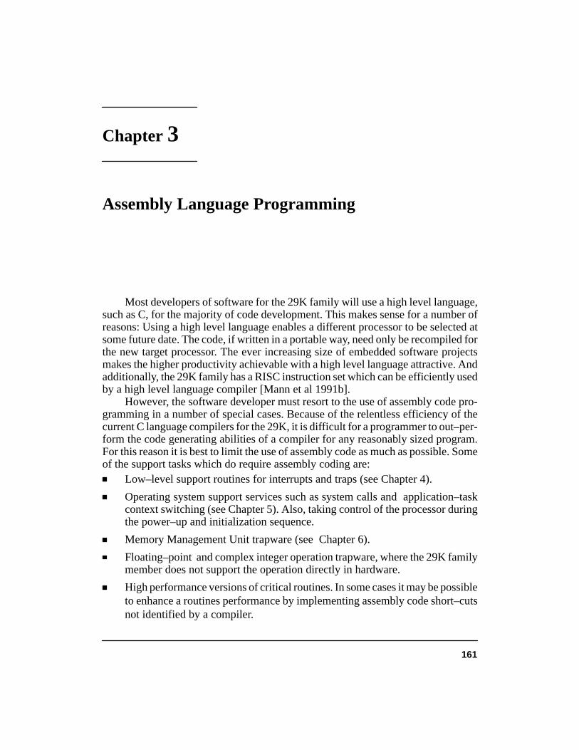
161
Chapter 3
Assembly Language Programming
Most developers of software for the 29K family will use a high level language,such as C, for the majority of code development. This makes sense for a number ofreasons: Using a high level language enables a different processor to be selected atsome future date. The code, if written in a portable way, need only be recompiled forthe new target processor. The ever increasing size of embedded software projectsmakes the higher productivity achievable with a high level language attractive. Andadditionally, the 29K family has a RISC instruction set which can be efficiently usedby a high level language compiler [Mann et al 1991b].
However, the software developer must resort to the use of assembly code pro-gramming in a number of special cases. Because of the relentless efficiency of thecurrent C language compilers for the 29K, it is difficult for a programmer to out–per-form the code generating abilities of a compiler for any reasonably sized program.For this reason it is best to limit the use of assembly code as much as possible. Someof the support tasks which do require assembly coding are:
Low–level support routines for interrupts and traps (see Chapter 4).
Operating system support services such as system calls and application–taskcontext switching (see Chapter 5). Also, taking control of the processor duringthe power–up and initialization sequence.
Memory Management Unit trapware (see Chapter 6).
Floating–point and complex integer operation trapware, where the 29K familymember does not support the operation directly in hardware.
High performance versions of critical routines. In some cases it may be possibleto enhance a routines performance by implementing assembly code short–cutsnot identified by a compiler.

162 Evaluating and Programming the 29K RISC Family
This chapter deals with aspects of assembly level programming. There are somedifferences between 29K family members, particularly in the area of on–chip periph-erals for microcontrollers. The chapter does not go into details peculiar to individualfamily members; for that it is best to study the processor User’s Manual.The material covered is relevant to all 29K family members.
3.1 INSTRUCTION SET
The Am29000 microprocessor implements 112 instructions. All hardware im-plemented instructions execute in a single–cycle, except for IRET, IRETINV,LOADM and STOREM. Instruction format was discussed in section 1.11. Allinstructions have a fixed 32–bit format, with an 8–bit opcode field and 3, 8–bit, oper-and fields. Field–C specifies the result operand register (DEST), field–A and field–Bsupply the source operands (SRCA and SRCB). Most instructions operate on dataheld in global or local registers, and there are no complex addressing modes sup-ported. Field–B, or field–B and field–A combined, can be used to provide 8–bit or16–bit immediate data for instructions. Access to external memory can only be per-formed with the LOAD[M] and STORE[M] instructions. There are a number ofinstructions, mostly used by operating system code, for accessing the processor spe-cial registers.
The following sections deal with the different instruction classes. Some of theinstructions described are not directly supported by all members of the 29K family.In particular, many of the floating–point instructions are only directly executed bythe Am29050 processor. If an instruction is not directly supported by the processorhardware, then a trap is generated during instruction execution. In this case, the oper-ating system uses trapware to implement the instruction’s operation in software.Emulating nonimplemented instructions in software means some instruction execu-tion speeds are reduced, but the instruction set is compatible across all family mem-bers.
3.1.1 Integer Arithmetic
The Integer Arithmetic instructions perform add, subtract, multiply, and divideoperations on word–length (32–bit) integers. All instructions in this class set theALU Status Register. The integer arithmetic instructions are shown Tables 3–1 and3–2.
The MULTIPLU, MULTIPLY, DIVIDE, and DIVIDU instructions are not im-plemented directly on most 29K family members, but are supported by traps. To de-termine if your processor directly supports these instructions, check with the proces-sor User’s Manual or the tables in Chapter 1. The Am29050 microprocessor supportsthe multiply instructions directly but not the divide instructions.

Chapter 3 Assembly Language Programming 163
Mnemonic Operation Description
ADDS DEST <– SRCA + SRCBIF signed overflow THEN Trap (Out Of Range)
ADD DEST <– SRCA + SRCB
ADDU DEST <– SRCA + SRCBIF unsigned overflow THEN Trap (Out Of Range)
ADDCS DEST <– SRCA + SRCB + C (from ALU)IF signed overflow THEN Trap (Out Of Range)
ADDC DEST <– SRCA + SRCB + C (from ALU)
ADDCU DEST <– SRCA + SRCB + C (from ALU)IF unsigned overflow THEN Trap (Out Of Range)
SUBS DEST <– SRCA – SRCBIF signed overflow THEN Trap (Out Of Range)
SUB DEST <– SRCA – SRCB
SUBU DEST <– SRCA – SRCBIF unsigned underflow THEN Trap (Out Of Range)
SUBCS DEST <– SRCA – SRCB – 1 + C (from ALU)IF signed overflow THEN Trap (Out Of Range)
SUBC DEST <– SRCA – SRCB – 1 + C (from ALU)
SUBCU DEST <– SRCA – SRCB – 1 + C (from ALU)IF unsigned underflow THEN Trap (Out Of Range)
SUBRS DEST <– SRCB – SRCAIF signed overflow THEN Trap (Out Of Range)
SUBR DEST <– SRCB – SRCA
SUBRU DEST <– SRCB – SRCAIF unsigned underflow THEN Trap (Out Of Range)
SUBRC DEST <– SRCB – SRCA – 1 + C (from ALU)
(continued)
Table 3-1. Integer Arithmetic Instructions

164 Evaluating and Programming the 29K RISC Family
MUL Perform one–bit step of a multiply operation (signed)
MULL Complete a sequence of multiply steps
MULU Perform one–bit step of a multiply operation (unsigned)
DIVIDE DEST <– (Q//SRCA)/SRCB (signed)
DIV0 Intitialize for a sequence of divide steps (unsigned)
DIV Perform one–bit step of a divide operation (unsigned)
DIVL Complete a sequence of divide steps (unsigned)
DIVREM Generate remainder for divide operation (unsigned)
DIVIDU DEST <– (Q//SRCA)/SRCB (unsigned)Q <– Remainder
Q <– Remainder
MULTIPLY Q//DEST <– SRCA * SRCB (signed)
SUBRCU DEST <– SRCB – SRCA – 1 + C (from ALU)IF unsigned underflow THEN Trap (Out Of Range)
SUBRCS DEST <– SRCB – SRCA – 1 + C (from ALU)IF signed overflow THEN Trap (Out Of Range)
MULTIPLU Q//DEST <– SRCA * SRCB (unsigned)
Mnemonic Operation Description
(continued)
Table 3-2. Integer Arithmetic Instructions (Concluded)
3.1.2 Compare
The Compare instructions test for various relationships between two values.For all Compare instructions except the CPBYTE instruction, the comparisons areperformed on word–length signed or unsigned integers. There are two types ofcompare instruction. The first writes a Boolean value into the result register (selectedby the instruction DEST operand) depending on the result of the comparison. ABoolean TRUE value is represented by a 1 in the most significant bit position. ABoolean FALSE is defined as a 0 in the most significant bit. The 29K uses a global orlocal register to contain the comparison result rather than the ALU status register.This offers a performance advantage as there is less conflict over access to a single

Chapter 3 Assembly Language Programming 165
shared resource. Compare instructions are frequently followed by conditional Jumpor Call instructions which depend on the contents of the compare result register.
The second type of compare instruction incorporates a conditional test in thesame instruction cycle accomplishing the comparison. These type of instructions,known as Assert instructions, allow instruction execution to continue only if the re-sult of the comparison is TRUE. Otherwise a trap to operating system code is taken.The trap number is supplied in the field–C (DEST) operand position of the instruc-tion. Trap numbers 0 to 63 are reserved for Supervisor mode program use. If an As-sert instruction, with trap number less than 64 is attempted while the processor is op-erating in User mode, a protection violation trap will be taken. Note, this is will occureven if the assertion would have been TRUE. Assert instructions are used in proce-dure prologue and epilogue routines to perform register stack bounds checking (seeChapter 2). Their fast operation makes them ideal for reducing the overhead of regis-ter stack support. They are also used as a means of requesting an operating systemsupport service (system call). In this case a condition known to be FALSE is asserted,and the trap number for the system call is supplied in instruction field–C. TheCompare instructions are shown in Tables 3–3 and 3–4.
The CPBYTE performs four comparisons simultaneously. The four bytes in theSRCA operand are compared with the SRCB operand and if any of them match thenBoolean TRUE is placed in the DEST register. The instruction can be very efficientlyused when scanning character strings. In particular, the C programming languagemarks the end of character strings with a 0 value. Using the CPBYTE instruction withSRCB supplying an immediate value 0, the string length can be quickly determined.
3.1.3 Logical
The Logical instructions perform a set of bit–by–bit Boolean functions onword–length bit strings. All instructions in this class set the ALU Status Register.These instructions are shown in Table 3-5.
3.1.4 Shift
The Shift instructions (Table 3-6) perform arithmetic and logical shifts on glob-al and local register data. The one exception is the EXTRACT instruction which op-erates on double–word data. When EXTRACT is used, SRCA and SRCB operandregisters are concatenated to form a 64–bit data value. This value is then shifted bythe funnel shifter by the amount specified by the Funnel Shift Count register (FC).The high order 32–bits of the shifted result are placed in the DEST register. The fun-nel shifter can be used to perform barrel shift and rotate operations in a single cycle.Note, when the SRCA and SRCB operands are the same register, the 32–bit operandis effectively rotated. The result may be written back to the same register or placed ina different global or local register (see Figure 3-1). The funnel shifter is useful forfixing–up unaligned memory accesses. The two memory words holding the un-

166 Evaluating and Programming the 29K RISC Family
Mnemonic Operation Description
CPEQ IF SRCA = SRCB THEN DEST <– TRUEELSE DEST <– FALSE
CPNEQ IF SRCA <> SRCB THEN DEST <– TRUEELSE DEST <– FALSE
CPLT IF SRCA < SRCB THEN DEST <– TRUEELSE DEST <– FALSE
CPLTU IF SRCA < SRCB (unsigned) THEN DEST <– TRUEELSE DEST <– FALSE
CPLE IF SRCA <= SRCB THEN DEST <– TRUEELSE DEST <– FALSE
CPLEU IF SRCA <= SRCB (unsigned) THEN DEST <– TRUEELSE DEST <– FALSE
CPGT IF SRCA > SRCB THEN DEST <– TRUEELSE DEST <– FALSE
CPGTU IF SRCA > SRCB (unsigned) THEN DEST <– TRUEELSE DEST <– FALSE
(continued)
Table 3-3. Compare Instructions
aligned data can be loaded into global registers, and then aligned by the EXTRACTinstruction into the destination register. A code example showing the rotate operationof the funnel shifter is given below:
mtsrim fc,8 ;rotate 8–bits leftextract gr96,gr97,gr97 ;source in gr97
SRCA operand SRCB operand
DEST register
Figure 3-1. The EXTRACT Instruction uses the Funnel Shifter
Funnel shiftcount, FC
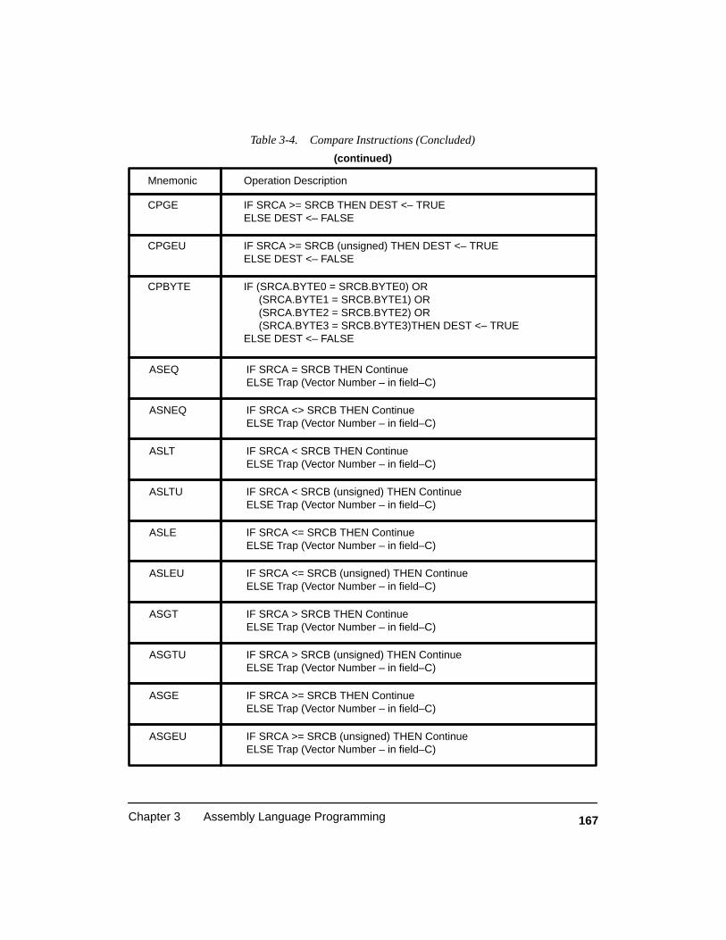
Chapter 3 Assembly Language Programming 167
CPGE IF SRCA >= SRCB THEN DEST <– TRUEELSE DEST <– FALSE
CPGEU IF SRCA >= SRCB (unsigned) THEN DEST <– TRUEELSE DEST <– FALSE
CPBYTE IF (SRCA.BYTE0 = SRCB.BYTE0) OR (SRCA.BYTE1 = SRCB.BYTE1) OR (SRCA.BYTE2 = SRCB.BYTE2) OR (SRCA.BYTE3 = SRCB.BYTE3)THEN DEST <– TRUEELSE DEST <– FALSE
ASEQ IF SRCA = SRCB THEN ContinueELSE Trap (Vector Number – in field–C)
ASNEQ IF SRCA <> SRCB THEN ContinueELSE Trap (Vector Number – in field–C)
ASLT IF SRCA < SRCB THEN ContinueELSE Trap (Vector Number – in field–C)
ASLTU IF SRCA < SRCB (unsigned) THEN ContinueELSE Trap (Vector Number – in field–C)
ASLE IF SRCA <= SRCB THEN ContinueELSE Trap (Vector Number – in field–C)
ASLEU IF SRCA <= SRCB (unsigned) THEN ContinueELSE Trap (Vector Number – in field–C)
ASGT IF SRCA > SRCB THEN ContinueELSE Trap (Vector Number – in field–C)
ASGTU IF SRCA > SRCB (unsigned) THEN ContinueELSE Trap (Vector Number – in field–C)
ASGE IF SRCA >= SRCB THEN ContinueELSE Trap (Vector Number – in field–C)
ASGEU IF SRCA >= SRCB (unsigned) THEN ContinueELSE Trap (Vector Number – in field–C)
Mnemonic Operation Description
(continued)
Table 3-4. Compare Instructions (Concluded)

168 Evaluating and Programming the 29K RISC Family
Mnemonic Operation Description
AND DEST <– SRCA & SRCB
ANDN DEST <– SRCA & ~ SRCB
DEST <– ~ (SRCA & SRCB)
OR DEST <– SRCA | SRCB
NOR DEST <– ~ (SRCA | SRCB)
XOR DEST <– SRCA ^ SRCB
XNOR DEST <– ~ (SRCA ^ SRCB)
NAND
Table 3-5. Logical Instructions
Mnemonic Operation Description
SLL DEST <– SRCA << SRCB (zero fill)
SRL DEST <– SRCA >> SRCB (zero fill)
DEST <– SRCA >> SRCB (sign fill)SRA
DEST <– high–order word of (SRCA//SRCB << FC)EXTRACT
Table 3-6. Shift Instructions
3.1.5 Data Movement
The Data Movement instructions (Tables 3–7 and 3–8) move bytes, half–words,and words between processor registers. In addition, the LOAD[M] and STORE[M]instructions move data between general–purpose registers and external devices, me-mories or coprocessor. The Am29050 processor has two additional instructions notshown in Table 3-7. They are MFACC and MTACC; and are used to access the fourdouble–word floating point accumulators (see section 3.3.5).

Chapter 3 Assembly Language Programming 169
Mnemonic Operation Description
LOAD DEST <– EXTERNAL WORD [SRCB]
LOADL DEST <– EXTERNAL WORD [SRCB]assert *LOCK output during access
LOADSET DEST <– EXTERNAL WORD [SRCB]EXTERNAL WORD [SRCB] <– h’FFFFFFFF’,assert *LOCK output during access
LOADM DEST.. DEST + COUNT <– EXTERNAL WORD [SRCB] ..EXTERNAL WORD [SRCB + COUNT * 4]
STORE EXTERNAL WORD [SRCB] <– SRCA
STOREM EXTERNAL WORD [SRCB] ..EXTERNAL WORD [SRCB + COUNT * 4] <– SRCA .. SRCA + COUNT
EXBYTE DEST <– SRCB, with low–order byte replaced by byte in SRCA selected by BP
EXHW DEST <– SRCB, with low–order half–word replaced by half–word in SRCA selected by BP
EXHWS DEST <– half–word in SRCA selected by BP, sign–extended to 32 bits
INBYTE DEST <– SRCA, with byte selected by BP replaced by low–order byte of SRCB
INHW DEST <– SRCA, with half–word selected by BP replaced by low–order half–word of SRCB
MFSR DEST <– SPECIAL
MFTLB DEST <– TLB [SRCA]
MTSR SPDEST <– SRCB
STOREL EXTERNAL WORD [SRCB] <– SRCAassert *LOCK output during access
(continued)
Table 3-7. Data Move Instructions

170 Evaluating and Programming the 29K RISC Family
Mnemonic Operation Description
MTSRIM SPDEST <– 0I16 (16–bit date formed with SRCA and SCRB fields
MTTLB TLB [SRCA] <– SRCB
(continued)Table 3-8. Data Move Instructions (Concluded)
The LOAD and STORE instructions are most interesting (see Figure 3-2 for theinstruction format). Instruction field–C is assigned a number of bit–field tasks whichcontrol the external access operation. Bit CE, when set, indicates that the data trans-fer is to coprocessor space. AMD makes a floating–point coprocessor, Am29027,which was frequently used with the Am29000 processor before the Am29050 pro-cessor became available. Because the Am29050 directly supports floating–pointinstructions there are no new designs making use of the Am29027 coprocessor.
31 23 15 7 0
X X X X X X X M 0 OPT RA RB or I
AS
PA
SB
UA
Figure 3-2. LOAD and STORE Instruction Format
CE
Bit field AS when set is used to indicate that the access is to Input/Output (I/O)space. I/O space is little used as there is no convenient means of accessing it from ahigh level language such as C. For this reason peripheral devices are typicallymapped into external data memory space rather than I/O space.
The PA and UA bits are used by Supervisor mode code; PA is used by operatingsystems which run with address translation turned on, but need to to access an exter-nal memory physical address. When bit PA is set, address translation is turned off forthe LOAD or STORE data access. This is useful when accessing peripheral devices.When operating system code wishes to access a User’s code space, it sets the UA bit.This causes the data transfer operation to execute with User rather than Supervisorpermission. If the User mode program was running with address translation on then,the PID field of the MMU register is used when checking TLB access permissions.Normally Supervisor mode code operates with a fixed PID value of zero.

Chapter 3 Assembly Language Programming 171
The original versions of the Am29000 processor (rev–A to rev–B) did not sup-port byte sized access to external memory. For this reason bytes and half–words hadto be extracted from words after they had been read from memory; the Extract Byte(EXBYTE) and Extract half–word (EXHW) instructions are supported by the pro-cessor for just this purpose. Additionally, when data objects smaller than a word werewritten to external memory, a read–modify–write process had to be used. The InsertByte (INBYTE) and Insert half–word (INHW) instructions supported the process.
Rev–C and later versions of the Am29000 processor and all other 29K familymembers directly support byte and half–word accesses to memory. The instructionsdescribed above need no longer be used. To enable current versions of the Am29000processor to be compatible with the original processor, the DW bit was added to theprocessor configuration register (CFG). When the DW bit is clear the processor per-forms rev–A type memory accesses. All new designs operate with the DW bit set; andother 29K family members operate with an implied DW bit set.
The OPT field bits specify the size of the data object being moved. They are alsoused to indicate a word sized access to Instruction ROM space is requested. Externallogic must be incorporated in a memory system design if this option is to be sup-ported. The OPT field appears on the OPT(2:0) output pins during the memory ac-cess. It is important that the object size is consistent with the address boundaries de-fined by the lower bits of the memory address. For example, if a word sized access(OPT filed value is 0) is attempted with lower address bits aligned to a byte boundary(A[1:0] not equal 0) then an unaligned access trap may occur. The Unaligned Access(UA) bit of the Current Processor Status (CPS) register must be set for the trap to betaken. Additionally, alignment checking is only performed for instruction and datamemory, not for I/O or coprocessor space accesses.
The SB bit is used when reading bytes or half–words from external memory.Sub–word sized accesses are determined by the OPT field; the processor right–justi-fies the accessed data within the destination register. The SB bit when set causes theremainder of the destination to be sign extended with the sign of the loaded data ob-ject. When SB is clear, the destination register value is zero–extended. The SB bit hasno effect during external memory writes. During write operations, the data object isreplicated in all positions of the data bus. For example, a byte write would result in thestored byte appearing in all four positions of the stored word. It is the responsibility ofexternal memory to decode the OPT field and lower address bits when determiningwhich byte position should be written. Note, the micorcontroller members of the 29Kfamily implement the memory glue logic on–chip.
Instruction field–B (SRCB) supplies the external memory address for LOADand STORE instructions. Typically a CONST, or CONST and CONSTH, instructionsequences precedes the LOAD or STORE instruction and establishes the access ad-dress for memory. However, the first 256 bytes of memory can be accessed with im-mediate addressing, where the 8–bit SRCB value contains the address. Some systems

172 Evaluating and Programming the 29K RISC Family
may be able to make use of this feature where performance is critical and the use ofCONST type instructions is to be avoided.
As described in Chapter 1, the use of LOAD and STORE instructions can effectthe processor pipeline utilization. Members of the 29K family which support a Har-vard memory architecture, or contain on–chip instruction memory cache, can per-form LOAD and STORE operations in parallel with other instructions. This preventspipeline stalling, as the instruction execution sequence can continue in parallel withthe external memory access. However, if the instruction following a LOAD operateson the accessed data then pipeline stalling will still occur. For this reason LOADinstructions should be positioned early in the instruction sequence, enabling the datamemory access latency to be hidden. Pipeline stalling will also occur if LOAD andstore type instructions are placed back–to–back, as this can result in channel accessconflicts. For this reason, LOAD and Store instructions should be separated with oth-er instructions as much as possible
3.1.6 Constant
The Constant instructions (Table 3-9) provide the ability to place half–word andword constants into registers. Most instructions in the instruction set allow an 8–bitconstant as an operand. The Constant instructions allow the construction of largerconstants. The Am29050 processor has an additional instruction, CONSTHZ, notsupported in other 29K family members. It places a 16–bit constant in the upper half–word position while the lower 16–bits are zero filled.
Mnemonic Operation Description
CONST DEST <– 0I16 (16–bit date formed with SRCA and SCRB fields
CONSTH
CONSTN DEST <– 1I16
Replace high–order half–word of SRCA by I16
Table 3-9. Constant Instructions

Chapter 3 Assembly Language Programming 173
3.1.7 Floating–point
The Floating–Point instructions (Tables 3–10 and 3–11) provide operations onsingle–precision (32–bit) or double–precision (64–bit) floating–point data. In addi-tion, they provide conversions between single–precision, double–precision, and in-teger number representations. In most 29K family members, these instructions causetraps to routines which perform the floating–point operations in software. TheAm29050 processor supports all floating–point instructions directly in hardware. Italso has four additional instructions not shown in Tables 3–10 and 3–11. They areMFAC ,DMAC and FMSM, DMSM; and are used to to perform single and double–precision multiply–and–accumulate type instructions (see section 3.3.5).
3.1.8 Branch
The Branch instructions (Table 3-12) control the execution flow of instructions.Branch target addresses may be absolute, relative to the Program Counter (with theoffset given by a signed instruction constant), or contained in a general–purpose reg-ister (indirect addressing). For conditional jumps, the outcome of the jump is basedon a Boolean value in a general–purpose register. Only the most significant bit in thespecified condition register is tested, Boolean TRUE is defined as bit–31 being set.Procedure calls are unconditional, and save the return address in a general–purposeregister. All branches have a delayed effect; the instruction following the branch isexecuted regardless of the outcome of the branch.
The instruction following the branch instruction is referred to as the delay slotinstruction. Assembly level programmers may have some difficulty in always find-ing a useful instruction to put in the delay slot. It is best to find an operation requiredregardless of the outcome of the branch. As a last resort a NOP instruction can beused, but this makes no effective use of the processor pipeline. When programmingin a high level language the compiler is responsible for making effective use of delayslots. Programmers not familiar with delayed branching often forget the delay slot isalways executed, with unfortunate consequences. For this reason, the example codethroughout this book shows delay slot instructions indented one space compared toother instructions. This has proven to be a useful reminder.
The delay slots of unconditional branches are easier to fill than conditionalbranches. The instruction at the target of the branch can be moved to, or duplicated at,the delay slot; and the jump address can be changed to the instruction following theoriginal target instruction.
The JMPFDEC instruction is very useful for implementing control loops basedon a decrementing loop. The counter register (SRCA) is first tested to determine if thevalue is FALSE, then it is decremented. The jump is then taken if a FALSE value wasdetected. The code example below shows how count words of external memory canbe written with zero. Note how the address pointer is incremented in the delay slot ofthe jump instruction. Additionally, the SRCA register must be initialized to count–2;

174 Evaluating and Programming the 29K RISC Family
Mnemonic Operation Description
FADD DEST (single–precision) <– SRCA (single–precision) + SRCB (single–precision)
DADD DEST (double–precision) <– SRCA (double–precision) + SRCB (double–precision)
FSUB DEST (single–precision) <– SRCA (single–precision) – SRCB (single–precision)
DSUB DEST (double–precision) <– SRCA (double–precision) – SRCB (double–precision)
FMUL DEST (single–precision) <– SRCA (single–precision) * SRCB (single–precision)
DMUL DEST (double–precision) <– SRCA (double–precision) * SRCB (double–precision)
FDIV DEST (single–precision) <– SRCA (single–precision)/ SRCB (single–precision)
DDIV DEST (double–precision) <– SRCA (double–precision)/ SRCB (double–precision)
FEQ IF SRCA (single–precision) = SRCB (single–precision) THEN DEST <– TRUEELSE DEST <– FALSE
DEQ IF SRCA (double–precision) = SRCB (double–precision) THEN DEST <– TRUEELSE DEST <– FALSE
FGE IF SRCA (single–precision) >= SRCB (single–precision) THEN DEST <– TRUEELSE DEST <– FALSE
DGE IF SRCA (double–precision) >= SRCB (double–precision) THEN DEST <– TRUEELSE DEST <– FALSE
FGT IF SRCA (single–precision) > SRCB (single–precision) THEN DEST <– TRUEELSE DEST <– FALSE
(continued)
Table 3-10. Floating–Point Instructions

Chapter 3 Assembly Language Programming 175
Mnemonic Operation Description
IF SRCA (double–precision) = SRCB (double–precision) THEN DEST <– TRUEELSE DEST <– FALSE
SQRT
CONVERT
CLASSDEST (single–precision, double–precision, extended–precision)<–CLASS[SRCA (single–precision, double–precision, extended–precision)]
DGT
DEST (integer,single–precision, double–precision)<–SRCA (integer, single–precision, double–precision)
DEST (single–precision, double–precision, extended–precision)<–SQRT[SRCA (single–precision, double–precision, extended–precision)
(continued)
Table 3-11. Floating–Point Instructions (Concluded)
this is because the loop is taken when the count value is 0 and –1, because the countdecrement is performed after the condition test. In practice, memory systems sup-porting burst–mode accesses could alternatively use a STOREM instruction to moreefficiently clear data memory.
const gr97,count–2 ;establish loop countconst gr98,0const gr96,address ;establish memory addressconsth gr96,address
clear: store 0,0,gr98,gr96 ;write zero to memoryjmpfdec gr97,clear ;test and decrement count add gr96,gr96,4 ;advance pointer
;arrive here when loop finished, gr97=–2
3.1.9 Miscellaneous Instructions
The Miscellaneous instructions (Table 3-13) perform various operations whichcannot be grouped into other instruction classes. In certain cases, these are controlfunctions available only to Supervisor–mode programs.
The Count Leading Zeros instruction can be very useful to assembly level pro-grammers. It determines the position of the most–significant one bit in the SRCBoperand. If all bits are zero, then 32 is returned. The instruction is useful when deter-mining priorities for, say, queues of interrupt requests, where each interrupt may set abit in the register operated on. The highest priority interrupt in the queue can bequickly determined by the CLZ instruction.
176 Evaluating and Programming the 29K RISC Family
Mnemonic Operation Description
CALL DEST <– PC//00 + 8PC <– TARGETExecute delay instruction
CALLI DEST <– PC//00 + 8PC <– SRCBExecute delay instruction
JMP PC <– TARGETExecute delay instruction
JMPI PC <– SRCBExecute delay instruction
JMPT IF SRCA = TRUE THEN PC <– TARGETExecute delay instruction
JMPTI IF SRCA = TRUE THEN PC <– SRCBExecute delay instruction
JMPF IF SRCA = FALSE THEN PC <– TARGETExecute delay instruction
JMPFI IF SRCA = FALSE THEN PC <– SRCBExecute delay instruction
JMPFDEC IF SRCA = FALSE THEN SRCA <– SRCA – 1 PC <– TARGETELSE SRCA <– SRCA – 1Execute delay instruction
Table 3-12. Branch Instructions
3.1.10 Reserved Instructions
The remaining operation codes are reserved for instruction emulation. Theseinstructions cause traps, much like the unimplemented floating–point instructions,but currently have no specified interpretation. The relevant operation codes, and thecorresponding trap vectors are given in the processor User’s Manual.
These instructions are intended for future processor enhancements, and usersdesiring compatibility with future processor versions should not use them for anypurpose.
The software developer should be aware of the trap taken with the reservedinstruction opcode 0xff. When execution is attempted with this opcode a trap 63 is

Chapter 3 Assembly Language Programming 177
Mnemonic Operation Description
CLZ Determine number of leading zeros in a word
SETIP Set IPA, IPB, and IPC with operand register–numbers
EMULATE Load IPA and IPB with operand register–numbers, and Trap VectorNumber in field–C
INV [ID] INV reset all Valid bits in instruction and data cachesINV 1; reset all Valid bits in instruction cacheINV 2; reset all Valid bits in data cache
IRET perform an interrupt return sequence
IRETINV [ID] IRETINV perform an interrupt return and invalidate all cachesIRETINV 1; perform an interrupt return and invalidate instruction cacheIRETINV 2; perform an interrupt return and invalidate date cache
HALT Enter Halt mode on next cycle
Table 3-13. Miscellaneous Instructions
taken. This can occur when a program goes out–of–control and attempts to fetchinstructions from nonexistent memory.
3.2 CODE OPTIMIZATION TECHNIQUES
When a high level programming language is used for software development,code optimization is left to the compiler. With assembly language programming, caremust be taken to avoid code sequences which impact upon the processor’s perfor-mance. Section 3.1.5 described how LOAD and STORE instruction must be careful-ly positioned if pipeline stalling is to be avoided. Section 3.1.8 discussed the delayslot of branch instructions, and the importance of finding a useful instruction fordelay slot filling. This section describes a few more useful coding techniques whichcan improve code execution performance.
Common Subexpression Elimination is a technique where a frequently occur-ring code sequence is eliminated to only one occurrence. This usually requires the

178 Evaluating and Programming the 29K RISC Family
result of the code sequence to be held in register space for frequent and fast access.The trade–off between expression reevaluation and consuming additional registerresources is easily made with the 29K family because of the large number of generalpurpose registers available. Code subexpressions need not be large. They may be asshort as an address calculation using a pair of CONST – CONSTH instructions. Thecalculation can be done once and the address kept around in a register for reuse.
Moving code out of loops is another technique frequently used to improve per-formance. However, the typically small number of registers in a CISC processor canoften mean loop invariant code results have to be held in external memory. This canlead to trade–offs between adding code within a loop or suffering the externalmemory access penalties. Again, the large number of general purpose registers in the29K assist the programmer to achieve improved code.
Branch instructions are to be avoided as their use impacts badly on perfor-mance. Processors supporting burst–mode addressing operate most efficiently wheninstruction bursting is not disrupted with a branch instruction. This is particularlytrue for memory systems which have a high first–access latency. The Branch TargetCache incorporated in some 29K family members can help hide the effects of branch-ing, but as the number of branch instructions is increased the chance of a hit occurringin the cache is reduced.
Loop Inversion is a useful technique at reducing the use of branch instructions.Often programmers will construct loops which have the loop condition test at the topof the loop. This requires a branch be used at the bottom of the loop. If the conditionalbranch is moved to the bottom of the loop then the number of branch instructions isreduced
3.3 AVAILABLE REGISTERS
In essence, global registers gr64–gr95 are reserved for interrupt handlers andthe operating system use. The remaining 32 global registers (gr96–gr127) are re-served for holding User mode program context. The high level language calling con-vention described in Chapter 2 established this convention. Figure 3-3 illustrates thepartitioning of the global registers among the operating system and user programtasks. General purpose registers 128–255 are better known as local registers, and ac-cessed via the registers stack pointer, gr1, rather than directly addressed as globalregisters. General purpose registers 128–255 can not be accessed like global registers(gr96–gr127); they can only be accessed as local registers or via indirect pointers.
The calling convention goes further than just dividing the register space into twogroups. The user space registers are assigned particular high level language supporttasks. All but four registers (gr112–gr115) in user task space will be accessed and mo-dified by compiler generated code at various times. Most of the registers are used ascompiler temporaries; three registers are used to support memory and register stacks;and the remaining four registers support the high level language procedure call

Chapter 3 Assembly Language Programming 179
Figure 3-3. General Purpose Register Usage
gr64
gr95gr96
gr127
Operating SystemStatics
ks0–ks15
Operating SystemTemporaries
Interrupt Handler
gr95
gr80gr79
gr67
gr64
Compiler Temporaries5 Global Registers
Reserved for Programer4 Global Registers
Function Return Values16 Global Registers
gr96–gr111
gr124
gr121gr120
gr116gr115
gr112gr111
gr96
Temporariesit0–it3
kt0–kt11 gr68
gr2
gr63
gr1
notimplemented
gr127gr126gr125
rfbrabmsp
Compiler Temporaries and
stack pointer
local registercache
UserTask
Space
Operatingsystem space
slplrptpc tav
static link pointerlarge return pointertrap return pointertrap argument vector
Register andMemory stacksupport
gr122gr123
255
128
mechanism and system calls. Global registers in the range gr121–gr127 are known tothe programmer by special synonym; however the registers themselves operate nodifferently from other global registers.
In particular gr121 (tav) and gr122 (tpc) are used to pass arguments to trap rou-tines invoked with Assert type instructions. This occurs during procedure prologueand epilogue as well as operating system service calls. At other times, the compileruses these registers to hold temporary data values.
Register gr123 (lrp) is known as the Large Return Pointer. It is used when a pro-cedure is required to return an object which is larger than 16 words and therefore can-not fit in the normal return space (gr96–gr111). The caller must assign lrp to point tomemory which will hold the 17th and higher words of return data.
Register gr124 (slp) is known as the Static Link Pointer. It is used when acces-sing data variables defined in a parent procedure. This occurs in some languages,Pascal for example, where nested procedure declarations are permitted. The High C29K and GNU compiler do not use this register unless C language extensions areused.

180 Evaluating and Programming the 29K RISC Family
A called procedure can locate its dynamic parent and the variables of the dy-namic parent because of the the caller–callee activation record linkage (see section3.5). However, the linkage is not adequate to locate variables of the static parentwhich may be referenced in the procedure. If such references appear in a procedure,the procedure must be provided with a local register which forms part of the staticlink pointer chain. Since there can be a hierarchy of static parents, the slp points to theslp of the immediate parent, which in turn points to the slp of its immediate parent.
The memory–stack support register gr125 (msp) and the register–stack supportregisters gr126 (rab), gr127 (rfb) and gr1 (rsp), were discussed in detail in Chapter 2.They maintain the current positions of the stack resources.
The calling convention does not assign any particular task to the registers in theoperating system (OS) group (gr64–gr95). However, over time a convention hasevolved among 29K processor users.The subdivision of the OS registers shown inFigure 3-3 is widely adhered to. The subgroups are known as: the interrupt freezemode temporaries (given synonyms it0–it3); the operating system temporaries(kt0–kt11); and the operating system statics support registers (ks0–ks15). Note, staticregister ks0 is often combined with it0–kt11 to form an interrupt context cache (seesection 2.5.1). Consequently, ks1 is the first available static support register.
When developing a new assembly language procedure a useful technique is toconstruct a C language routine which receives any passed parameters and imple-ments the appropriate task. With the AMD High C 29K compiler, the procedure canbe compiled to produce an assembly language output file with the “–S –Hanno” com-piler switches. The Assembly level code can then be directly modified into the re-quired code sequence.
3.3.1 Useful Macro–Instructions
The code examples shown in later chapters make use of a number macros forpushing and popping special registers to an external memory stack. A macro instruc-tion is composed of a sequence of simpler instructions. Effectively, a macro is an in–line procedure call. Using macros is faster than making an actual procedure call butconsumes more instruction memory space.The macro definitions are presented be-low:
.macro pushsr,sp,reg,sreg ;macro name and parametersmfsr reg,sreg ;copy from specialsub sp,sp,4 ;decrement pointerstore 0,0,reg,sp ;store on stack
.endm; .macro popsr,sreg,reg,sp ;macro name and parameters
load 0,0,reg,sp ;get from stackadd sp,sp,4 ;increment pointermtsr sreg,reg ;move to special
.endm
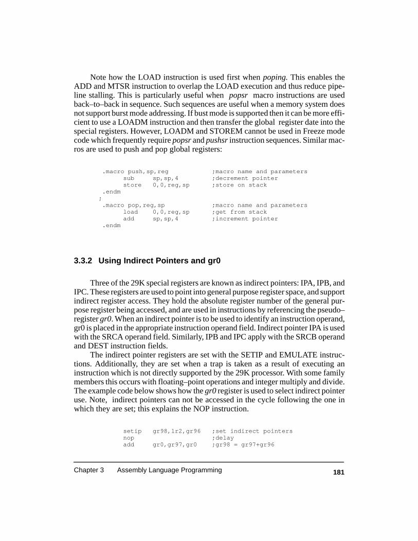
Chapter 3 Assembly Language Programming 181
Note how the LOAD instruction is used first when poping. This enables theADD and MTSR instruction to overlap the LOAD execution and thus reduce pipe-line stalling. This is particularly useful when popsr macro instructions are usedback–to–back in sequence. Such sequences are useful when a memory system doesnot support burst mode addressing. If bust mode is supported then it can be more effi-cient to use a LOADM instruction and then transfer the global register date into thespecial registers. However, LOADM and STOREM cannot be used in Freeze modecode which frequently require popsr and pushsr instruction sequences. Similar mac-ros are used to push and pop global registers:
.macro push,sp,reg ;macro name and parameterssub sp,sp,4 ;decrement pointerstore 0,0,reg,sp ;store on stack
.endm; .macro pop,reg,sp ;macro name and parameters
load 0,0,reg,sp ;get from stackadd sp,sp,4 ;increment pointer
.endm
3.3.2 Using Indirect Pointers and gr0
Three of the 29K special registers are known as indirect pointers: IPA, IPB, andIPC. These registers are used to point into general purpose register space, and supportindirect register access. They hold the absolute register number of the general pur-pose register being accessed, and are used in instructions by referencing the pseudo–register gr0. When an indirect pointer is to be used to identify an instruction operand,gr0 is placed in the appropriate instruction operand field. Indirect pointer IPA is usedwith the SRCA operand field. Similarly, IPB and IPC apply with the SRCB operandand DEST instruction fields.
The indirect pointer registers are set with the SETIP and EMULATE instruc-tions. Additionally, they are set when a trap is taken as a result of executing aninstruction which is not directly supported by the 29K processor. With some familymembers this occurs with floating–point operations and integer multiply and divide.The example code below shows how the gr0 register is used to select indirect pointeruse. Note, indirect pointers can not be accessed in the cycle following the one inwhich they are set; this explains the NOP instruction.
setip gr98,lr2,gr96 ;set indirect pointersnop ;delayadd gr0,gr97,gr0 ;gr98 = gr97+gr96

182 Evaluating and Programming the 29K RISC Family
The main use of indirect pointers is to support transparent routines (see section3.7) and instruction emulation. With most 29K family members the integer multiplyinstruction (MULTIPLY) is not directly supported.
multiply lr4,gr98,lr10 ;integer multiply, lr4 = gr98*lr10
On entering the trapware support routine for the vector assigned to the MUL-TIPLY instruction (vector number 32) the indirect pointers are set to IPC=lr4,IPA=gr98 and IPB=lr10 for the above example. This enables the trap handler to easi-ly and efficiently access the register operands for the instruction without having toexamine the actual instruction in memory.
When using a MTSRIM instruction to set an indirect pointer register value, it isimportant to remember that the most significant bit (bit position 9) must be set if localregisters are to be accessed. This is because indirect pointers operate with absoluteregister numbers. See the following section discussing the use of gr1 for more detailson register addressing.
3.3.3 Using gr1
Global register gr1 performs the special task of supporting indirect access of the128 local registers. When an instruction operand, say SRCA, has its top most bit setthen base–plus–offset addressing is used to access the operand. This means only gen-eral purpose registers in the range gr1–gr127 can be addressed via their absolute reg-ister number given the supported instruction operand decoding. (Indirect pointers en-able all general purpose registers to be accessed via absolute address numbers.) Thelower 7–bits of the operand supply the offset which is shifted left 2–bits then addedwith the local register base held in register gr1. Register gr1 is a 32–bit register, andbits 8–2 contain the local register base (see Figure 3-4).
31 23 15 7 0
Figure 3-4. Global Register gr1 Fields
local register base
2
0 0
The base offset calculation is performed modulo–128. The most significant ad-dress bit is assumed set when forming the absolute address for all local register ac-cesses.
29K processors use a shadow copy of the gr1 register when performing localregister addressing. The shadow copy can only be modified by an arithmetic or log-ical instruction; a shift or load into gr1 will not update the shadow copy. Because of

Chapter 3 Assembly Language Programming 183
the shadow register technique, there must be a delay of one cycle before the registerfile can be accessed after gr1 has been modified.
3.3.4 Accessing Special Register Space
The special registers control the operation of the processor. They are dividedinto two groups: those that can be accessed only in Supervisor mode and those whichhave unrestricted access. Access of special registers sr128 and above do not generatea protection violation when accessed in User mode. Special register space was de-scribed in section 1.10.2. Not all 29K family members have fully implemented spe-cial register spaces. In the Supervisor–only accessible space there are a number ofdifferences due to differences in on–chip resources such as cache memory and hard-ware breakpoint registers. Because these are not accessible to application code theydo not effect application code portability.
However, some members of the 29K family do not implement, in hardware, allof the special registers accessible by User mode programs. In particular the floatingpoint support registers (sr160–sr162) are only implemented on processors which di-rectly support floating–point instructions in hardware. All other family membersvirtualize these registers. An attempted access to unimplemented special registerscauses a Protection Violation trap to occur. The trapware code implements the accessand returns the result. Unfortunately, the trapware code does not use the indirectpointer as they are not set by a protection violation trap. This means the trapwaremust read the instruction space to determine the special register being accessed. Thisleads to the consequence that the special floating point support registers can not bevirtualized with Harvard memory architectures which do not provide a memorybridge to enable instruction memory to be accessed as data. The emulation techniquealso requires the support of three operating system registers. The trapware is typical-ly configured to use global registers ks13–ks15 (gr93–gr95) for this task.
Special registers are located in their own register space. They can only be ac-cessed by the move–from (MFSR) and move–to (MTSR) instructions which transferdata between special register space and general purpose registers. In addition there isa MTSRIM instruction which can be used to set a special register with 16–bit im-mediate data. The indirect pointers can not be used to access special register space.This imposes some restriction in accessing special registers but in practice is accept-able. However, where the address of a special register to be accessed is contained in ageneral purpose register, the technique shown below can be used. In the example, lr2contains the address of the special register to be read with a MFSR instruction. Theexample assumes instruction memory can be written to; the required instruction isbuilt in gr97 and stored in memory at an address given by gr98. The instruction isthen visited with a JMPI instruction. A jump instructions target address is visitedwhen the jump instruction contains a further jump in its delay slot. The second jumpis in the decode stage of the processor pipeline when the first jump is in execute. This

184 Evaluating and Programming the 29K RISC Family
means the second jump must be taken, and only the first instruction of the newinstruction stream is started before execution continues at label continue.
const gr98,I_memory ;establish instruction addressconsth gr98,I_memoryconst gr97,0xC6600000 ;MFSR, DEST=gr96, SRCA=0consth gr97,0xC6600000sll lr2,lr2,8 ;lr2 has special register numberor lr2,lr2,gr97 ;instruction now constructedstore 0,0,lr2,gr98 ;store target instructionjmpi gr98 ;visit the target instruction jmp continue ;must execute the delay slot
continue:
The constructed MFSR instruction places the result in register gr96. The lr2source address value had to be shifted left 8–bits into the SRCA field position of theMFSR instruction.
3.3.5 Floating–point Accumulators
The Am29050 processor is currently the only member of the 29K family whichdirectly supports in hardware floating–point arithmetic operations. In addition tosupporting floating–point operations without using trapware emulation, functionsinvolving multiply–and–accumulate operations are supported by four additionalhardware instructions not implemented in other 29K family members. Sum–of–product type operations are frequently required by many floating–point intensive ap-plications, such as matrix multiplication. Implementing this operation efficiently inhardware makes the Am29050 processor suitable for use in graphics and signal pro-cessing applications.
The FMAC and DMAC instructions can be used to multiply two general pur-pose register values together and sum the product with one of the four floating–pointaccumulators. The DMAC instruction operates on double–precision operand dataand the FMAC operates on single–precision. Double–precision operands can be ac-cessed from the register file in a single cycle as the register file is implemented as64–bits wide, and there is 64–bit wide ports supplying data to the floating–pointexecution unit components. Double–precision operands must be aligned on double–register address boundaries.
The FMSM and DMSM instructions support single and double–precision float-ing–point multiply–and–sum. One operand for the multiplication is a general pur-pose register, the second is accumulator 0; the product is summed with the secondinstruction operand and the result placed back in the register file. These two instruc-tions can be used when the multiplier is a fixed value such as with SAXPY (single–precision A times X plus Y).
The Floating–Point Unit on the Am29050 processor is constructed from a num-ber of specialized operation pipelines; one for addition/subtraction, one for multi-

Chapter 3 Assembly Language Programming 185
plication , and one for division/square root. The functional units used by the pipelinesall operate separately. This enables multiple floating–point instructions to be inexecute at the same time. Additionally floating–point operations can commence inparallel with operations carried out by the processor’s integer pipeline. The operationof some of the pipeline functional units can be multicycle and contention for re-sources can result if simultaneous floating–point operations are being performed.However, all floating–point operations are fully interlocked, and operations requir-ing the result of a previous functional unit operation are prevented from proceedinguntil that result is available. The programmer never has to become involved in thepipeline stage details to ensure the success of an operation.
To sustain efficient use of the floating–point pipelines, four floating–point accu-mulator registers are provided. The programmer must multiplex their use duringheavily pipelined code sequences to reduce resource contention. The Am29050 pro-cessor can issue a new floating–point instruction every cycle but many of the opera-tions have multicycle latency. Thus to avoid pipeline stalling, the results should notbe used until a sufficient number of delay cycles has passed (see Am29050 processorUser’s Manual). The processor has an additional 64–bit write port on the general pur-pose register file for use by the floating–point unit. This enables floating–point re-sults to be written back at the same time as integer pipeline results.
The floating–point accumulators can be accessed by the MTACC (move–to)and MFACC (move–from) instructions which are available to User mode code. Only29K family members which directly support floating–point operations implementthese instructions.
3.4 DELAYED EFFECTS OF INSTRUCTIONS
Modification of some registers has a delayed effect on processor behavior.When developing assembly code, care must be taken to prevent unexpected behav-ior. The easiest of the delayed effects to remember is the one cycle that must followthe use of an indirect pointer after having set it. This occurs most often with the regis-ter stack pointer. It cannot be used to access a local register in the instruction that fol-lows the instruction that writes to gr1. An instruction that does not require gr1 (andthat means all local registers referenced via gr1) can be placed immediately after theinstruction that updates gr1.
Direct modification of the CPS register must also be done carefully. Particularlywhere the freeze (FZ) bit is cleared. When the processor is frozen, the special-pur-pose registers are not updated during instruction execution. This means that the PC1register does not reflect the actual program counter value at the current execution ad-dress, but rather at the point where freeze mode was entered. When the processor isunfrozen, either by an interrupt return or direct modification of the CPS, two cyclesare required before the PC1 buffer register reflects the new execution address. Unlessthe CPS register is being modified directly, this creates no problem.
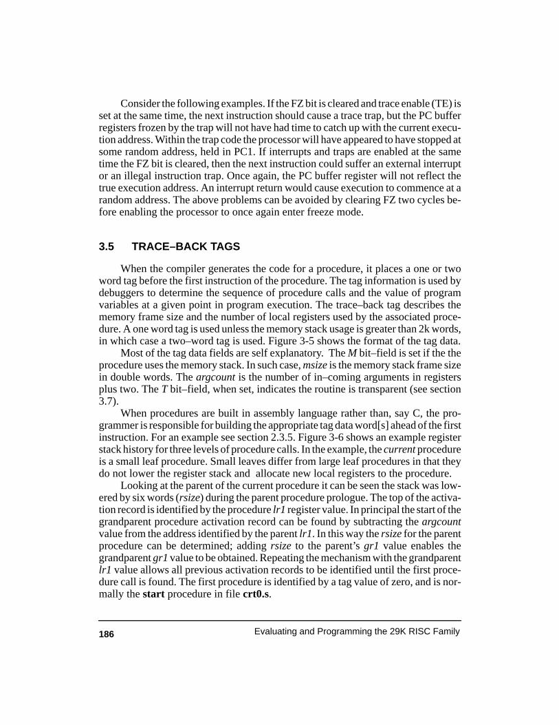
186 Evaluating and Programming the 29K RISC Family
Consider the following examples. If the FZ bit is cleared and trace enable (TE) isset at the same time, the next instruction should cause a trace trap, but the PC bufferregisters frozen by the trap will not have had time to catch up with the current execu-tion address. Within the trap code the processor will have appeared to have stopped atsome random address, held in PC1. If interrupts and traps are enabled at the sametime the FZ bit is cleared, then the next instruction could suffer an external interruptor an illegal instruction trap. Once again, the PC buffer register will not reflect thetrue execution address. An interrupt return would cause execution to commence at arandom address. The above problems can be avoided by clearing FZ two cycles be-fore enabling the processor to once again enter freeze mode.
3.5 TRACE–BACK TAGS
When the compiler generates the code for a procedure, it places a one or twoword tag before the first instruction of the procedure. The tag information is used bydebuggers to determine the sequence of procedure calls and the value of programvariables at a given point in program execution. The trace–back tag describes thememory frame size and the number of local registers used by the associated proce-dure. A one word tag is used unless the memory stack usage is greater than 2k words,in which case a two–word tag is used. Figure 3-5 shows the format of the tag data.
Most of the tag data fields are self explanatory. The M bit–field is set if the theprocedure uses the memory stack. In such case, msize is the memory stack frame sizein double words. The argcount is the number of in–coming arguments in registersplus two. The T bit–field, when set, indicates the routine is transparent (see section3.7).
When procedures are built in assembly language rather than, say C, the pro-grammer is responsible for building the appropriate tag data word[s] ahead of the firstinstruction. For an example see section 2.3.5. Figure 3-6 shows an example registerstack history for three levels of procedure calls. In the example, the current procedureis a small leaf procedure. Small leaves differ from large leaf procedures in that theydo not lower the register stack and allocate new local registers to the procedure.
Looking at the parent of the current procedure it can be seen the stack was low-ered by six words (rsize) during the parent procedure prologue. The top of the activa-tion record is identified by the procedure lr1 register value. In principal the start of thegrandparent procedure activation record can be found by subtracting the argcountvalue from the address identified by the parent lr1. In this way the rsize for the parentprocedure can be determined; adding rsize to the parent’s gr1 value enables thegrandparent gr1 value to be obtained. Repeating the mechanism with the grandparentlr1 value allows all previous activation records to be identified until the first proce-dure call is found. The first procedure is identified by a tag value of zero, and is nor-mally the start procedure in file crt0.s.
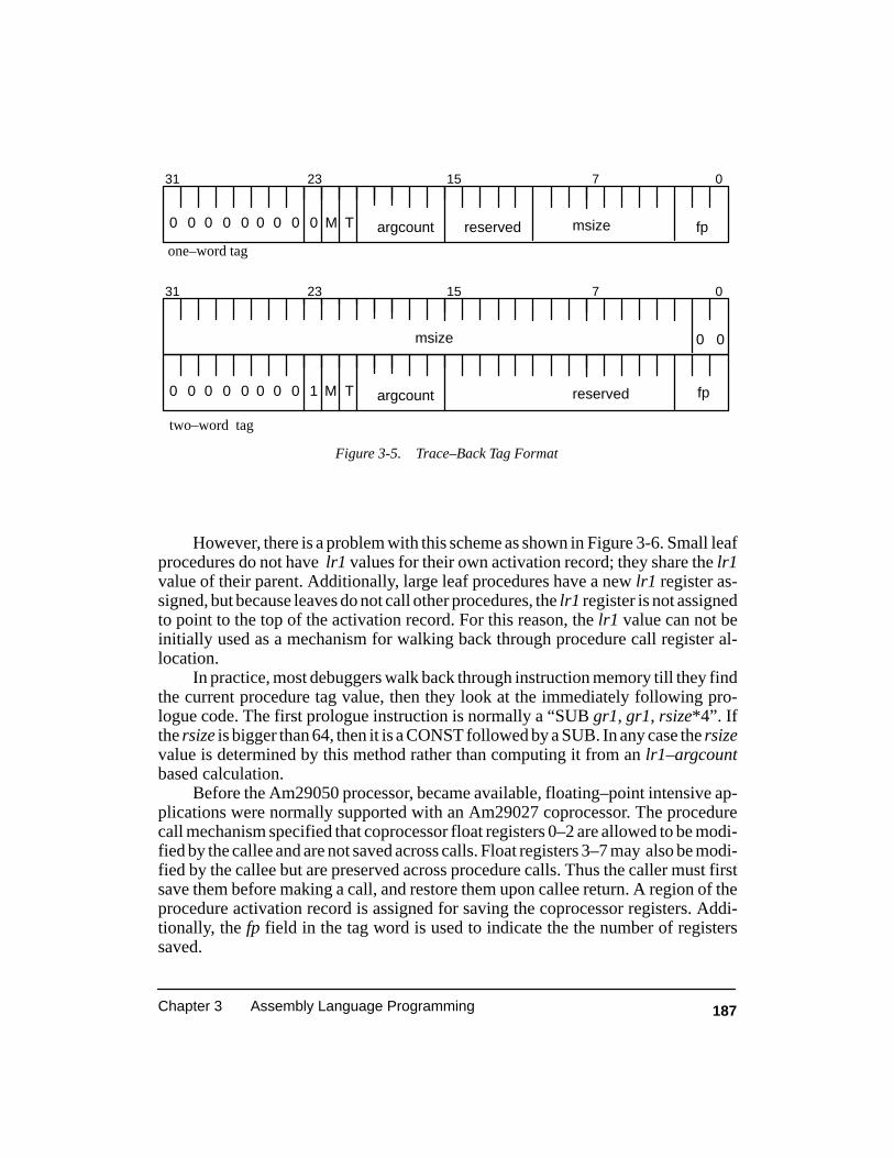
Chapter 3 Assembly Language Programming 187
31 23 15 7 0
argcount reserved fp
Figure 3-5. Trace–Back Tag Format
0 0 0 0 0 0 0 0 0 M T msize
31 23 15 7 0
0 0msize
argcount0 0 0 0 0 0 0 0 1 M T reserved
one–word tag
two–word tag
fp
However, there is a problem with this scheme as shown in Figure 3-6. Small leafprocedures do not have lr1 values for their own activation record; they share the lr1value of their parent. Additionally, large leaf procedures have a new lr1 register as-signed, but because leaves do not call other procedures, the lr1 register is not assignedto point to the top of the activation record. For this reason, the lr1 value can not beinitially used as a mechanism for walking back through procedure call register al-location.
In practice, most debuggers walk back through instruction memory till they findthe current procedure tag value, then they look at the immediately following pro-logue code. The first prologue instruction is normally a “SUB gr1, gr1, rsize*4”. Ifthe rsize is bigger than 64, then it is a CONST followed by a SUB. In any case the rsizevalue is determined by this method rather than computing it from an lr1–argcountbased calculation.
Before the Am29050 processor, became available, floating–point intensive ap-plications were normally supported with an Am29027 coprocessor. The procedurecall mechanism specified that coprocessor float registers 0–2 are allowed to be modi-fied by the callee and are not saved across calls. Float registers 3–7 may also be modi-fied by the callee but are preserved across procedure calls. Thus the caller must firstsave them before making a call, and restore them upon callee return. A region of theprocedure activation record is assigned for saving the coprocessor registers. Addi-tionally, the fp field in the tag word is used to indicate the the number of registerssaved.
188 Evaluating and Programming the 29K RISC Family
Figure 3-6. Walking Back Through Activation Records
lr5lr4lr3lr2lr1lr0
arg4arg3arg2arg1
arg2arg1
lr0lr1lr0
rsize=6
size=12
gr1
argcount=6
small leafactivationrecord
parentactivationrecord
grand parentactivationrecord
When using an Am29050 processor the fp field value is always zero. The fourdouble–word accumulator registers are not preserved across a procedure call. If aprocedure uses the accumulators and wishes to preserve their contents, it must firstsave them before making a procedure call. This may involve temporary modifyingthe special floating–point environment registers. Because the floating–point accu-mulators are normally accessed by assembly language leaf routines, caller saving ofthe accumulators results in a reduced overhead compared to callee saving.
3.6 INTERRUPT TAGS
The High C 29K compiler will place an additional tag word before the normalprocedure tag when the key word _Interrupt is used to define a procedure’s returntype. Figure 3-7 shows the typical tag word combination produced. The first proce-dure of an interrupt handler, that is the procedure accessed after the interrupt vector isprocessed and any necessary preparation work is performed, should be identified bythe _Interrupt key word. Examples of how interrupt tags are used by application codeis shown in section 2.5.4.
The second (or second and third) word of tag information has the same format asall procedure tags. Only the first tag word is new and this word is known as the inter-rupt tag word. It has several bit–fields which describe the execution environment re-quired by the procedure. These fields can be examined at interrupt occurrence time orat interrupt installation time to determine the appropriate steps required to preparethe interrupt processing environment. The objective is to optimize interrupt prepara-tion by only preserving the minimum required context. Of course, the exact steps tak-

Chapter 3 Assembly Language Programming 189
argcount reserved fp
Figure 3-7. Interrupt Procedure Tag Words
0 0 0 0 0 0 0 0 0 M T msize
31 23 15 7 0
local registerstemps.
normal one–word procedure tag
0 0 0 0 0 0 0 0 C
19
return registersQIF
interrupt tag
en will be very much dependant on the operating system in use. For example, someoperating systems may process interrupts in User mode with address translation inuse. Others may process interrupts in Supervisor mode with physical addressing.
The C bit is set if the procedure calls any other procedure (excluding transparentroutines). That is, the C bit is set if the procedure is not a child. When a another proce-dure is called, it may be necessary to have the register stack repaired before the firstprocedure is entered. The local registers bit–field indicates the number of registersrequired from the register stack cache. However, other procedures called by the firstprocedure may require additional local registers. Note that large leaf routines mayrequire local registers but of course the C bit will still not be set. When the C bit is set,preparation code is unlikely to scan the other bit–fields as it is usually necessary toassume that called functions may perform any 29K operation.
The F bit will be set if any floating–point operations are performed. Most 29Kfamily members do not directly support floating–point instructions but take a trapwhen a floating–point instruction is encountered. Trap handlers can not be enteredfrom Freeze mode and execution of a floating–point operation could modify the stateof floating–point accumulators (Am29050) or coprocessor (Am29027) status regi-setrs.
The I bit is set if any of the indirect pointer registers (IPA, IPB and IPC) are mo-dified by the procedure. These registers would be effected by a call to a transparenthelper routine which issues a trap. The High C 29K compiler uses a transparent rou-tine to perform integer multiply with most 29K family members. If the I bit is set theninterrupt preparation code would be required to preserve the indirect pointer registersbefore entering the first procedure. The Q bit is set when the Q register (sr131) is mo-dified. This registers is used during floating–point and integer multiply and divideemulation routines.
The 29K calling convention states that a procedure return its results in globalregisters gr96–gr111. An interrupt handler routines does not have any return value.However, it may use registers in this range to hold temporary values during proce-

190 Evaluating and Programming the 29K RISC Family
dure execution. The return registers bit–field indicates the number of registers used.Additionally, temporary registers can be obtained from register range gr116–gr120.In fact, the GNU compiler prefers allocate temporary registers in this range beforeallocation from the return registers range (see section 2.5.2). The temps. bit–field in-dices the number of registers modified in the range gr116–gr124. When interruptprocessing is accomplished with a leaf routine, these bit–fields enable only the mini-mum number of global registers to be saved before the interrupt handler procedure isentered.
3.7 TRANSPARENT ROUTINES
Transparent routines are used to support small highly efficient procedure calls.They are like small leaf procedures in that they do not lower the register stack andallocate a new activation record. They are unlike leaf procedures in that the onlyglobal registers which the caller does not expect to survive the call are tav (gr121) andtpc (gr122). They are normally used to support compiler specific support routinessuch as integer multiply (where the 29K hardware does not directly support this op-eration).
Parameters are passed to transparent routines using tav and the indirect pointerregisters. Return values are via tpc and possibly the modified register identified byindirect pointer ipc. Leaf procedures can call transparent routines without changingtheir status as leaf routines.
Newer versions of the High C 29K compiler enable the user to select proceduresfor implementation as transparent routines. For example, a procedure which wouldnormally be of return type “int” would be defined (and declared) as type “_Transpar-ent int”. The _Transparent key word extends the C language. Of course there are anumber of restrictions which apply to transparent routine construction: They canonly receive two in–coming parameters (passed via IPA and IPB); They must be oftype void or return an object of word–size or less (return values are passed via IPC);They must not perform any floating point (and some integer) operations which re-quire trapware support; And of course, they must not call any other procedures (evenif they are transparent).
3.8 INITIALIZING THE PROCESSOR
Reset mode is entered when the processor’s *RESET pin is activated. Thiscauses the Current Processor Status (CPS) register to be set to the Reset mode values;the processor operates in Supervisor mode with all data and instruction addresses be-ing physical (no address translation); all traps and interrupts are disabled and the pro-cessor Freeze mode bit is set. (See the Initialization section of the processor User’sManual for the exact CPS register setting.) Individual 29K family members have
Chapter 3 Assembly Language Programming 191
additional Reset mode conditions established, such as disabling cache memorywhere appropriate.
Instruction execution begins at address 0. For processors supporting bothInstruction memory space and read–only memory (ROM) space, ROM space is usedwhen fetching instructions from external memory. However, many Am29000 pro-cessor systems apply no distinction when decoding instruction and ROM memoryspace.
The programmer must establish control of the processor and available re-sources. Section 7.4 discusses how this is achieved with the OS–boot operating sys-tem. OS–boot is made available by AMD, and is used to implement a single–taskapplication environment which supports HIF (see Chapter 2) system call services.Because OS–boot is so freely available to the 29K community, it is convenient to usethe included processor start–up code sequence for any new designs.
3.9 ASSEMBLER SYNTAX
Assembly language, like all languages, has a character set and a set of grammarrules. Purchasers of the ASM29K assembly language tool package from AMD orother tool company, normally obtain a copy of the assembly language syntax specifi-cation. There are a number of assembler tools available and all of them comply (butnot always fully) with the AMD defined syntax for assembly level programming.
Many of the assemblers have options which are unique, but it has been my expe-rience that assemblers will generally accept code which is produced by any of theavailable compilers.
3.9.1 The AMD Assembler
The AMD assembly language tool package, ASM29K, was used to develop allof the assembly language examples shown in this book. The assembler, linker andlibrarian tools included in the package were developed by Microrec Research Inc.(MRI) for AMD. The tools are available on a number of platforms; the most popularbeing SUN and HP workstations and IBM PCs and compatibles. This section doesnot cover the details of the AMD assembler (as29) and its options as they are welldocumented in the literature supplied with each purchased tool package.
During the introduction of the Am29000 processor, AMD had a second assem-bly level tool package developed by Information Processing Techniques Corp. (IPT).This second tool chain forms the basis of a number of elaborate tool packages madeavailable by third party tool suppliers. All of the tool suppliers are listed in the AMDFusion29Ksm Catalogue [AMD 1992a][AMD 1993b]. Both assemblers fully com-ply with the AMD assembler syntax for 29K code. However, the librarian tools sup-plied with the different tool packages maintain library code in different formats. Thismeans libraries cannot be shared unless reformatting is applied.
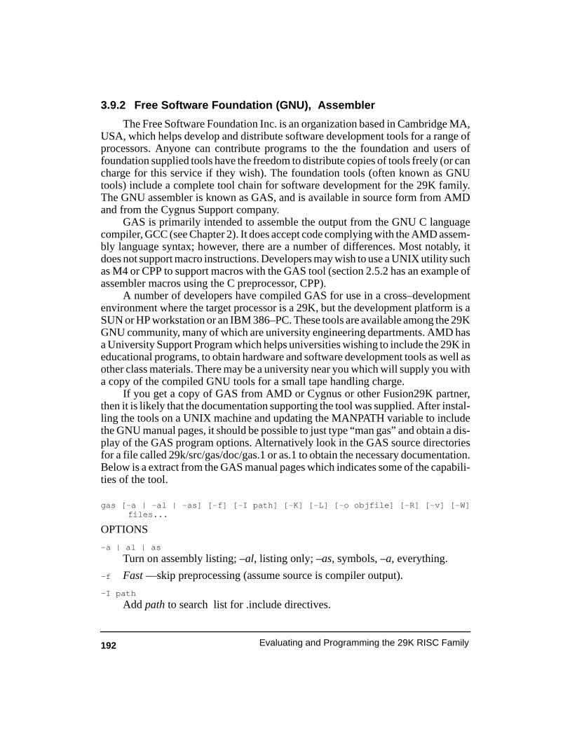
192 Evaluating and Programming the 29K RISC Family
3.9.2 Free Software Foundation (GNU), Assembler
The Free Software Foundation Inc. is an organization based in Cambridge MA,USA, which helps develop and distribute software development tools for a range ofprocessors. Anyone can contribute programs to the the foundation and users offoundation supplied tools have the freedom to distribute copies of tools freely (or cancharge for this service if they wish). The foundation tools (often known as GNUtools) include a complete tool chain for software development for the 29K family.The GNU assembler is known as GAS, and is available in source form from AMDand from the Cygnus Support company.
GAS is primarily intended to assemble the output from the GNU C languagecompiler, GCC (see Chapter 2). It does accept code complying with the AMD assem-bly language syntax; however, there are a number of differences. Most notably, itdoes not support macro instructions. Developers may wish to use a UNIX utility suchas M4 or CPP to support macros with the GAS tool (section 2.5.2 has an example ofassembler macros using the C preprocessor, CPP).
A number of developers have compiled GAS for use in a cross–developmentenvironment where the target processor is a 29K, but the development platform is aSUN or HP workstation or an IBM 386–PC. These tools are available among the 29KGNU community, many of which are university engineering departments. AMD hasa University Support Program which helps universities wishing to include the 29K ineducational programs, to obtain hardware and software development tools as well asother class materials. There may be a university near you which will supply you witha copy of the compiled GNU tools for a small tape handling charge.
If you get a copy of GAS from AMD or Cygnus or other Fusion29K partner,then it is likely that the documentation supporting the tool was supplied. After instal-ling the tools on a UNIX machine and updating the MANPATH variable to includethe GNU manual pages, it should be possible to just type “man gas” and obtain a dis-play of the GAS program options. Alternatively look in the GAS source directoriesfor a file called 29k/src/gas/doc/gas.1 or as.1 to obtain the necessary documentation.Below is a extract from the GAS manual pages which indicates some of the capabili-ties of the tool.
gas [–a | –al | –as] [–f] [–I path] [–K] [–L] [–o objfile] [–R] [–v] [–W] files...
OPTIONS
–a | al | as
Turn on assembly listing; –al, listing only; –as, symbols, –a, everything.
–f Fast ––skip preprocessing (assume source is compiler output).
–I path
Add path to search list for .include directives.

Chapter 3 Assembly Language Programming 193
–K Issue warning when difference tables altered for long displacements
–L Keep (in symbol table) local symbols starting with L.
–o objfile
Name the object–file output for GAS.
–R Fold data sections into text sections.
–v Announce GAS version.
–W Suppress warning messages.

194 Evaluating and Programming the 29K RISC Family

195
Chapter 4
Interrupts and Traps
This chapter describes techniques for writing interrupt and trap handlers for29K processor-based systems. It also describes the interrupt hardware for the 29KProcessor Family, and the software environment within which interrupt handlersexecute.
Handler descriptions are separated into two major sections. The first discussesSupervisor mode handlers and the second covers User mode handlers. Thedescriptions apply equally well to interrupts and traps. For the purposes of thischapter, User mode handlers refer to interrupt and trap handlers written in ahigh-order language. However, it is possible to enter User mode without firstestablishing high-order language support. Additionally, for our purposes we shallcall assembly level handlers Supervisor mode handlers.
Although interrupts are largely asynchronous events, traps most often occursynchronously with instruction execution; however, both share common logic in the29K Processor Family and are often handled entirely in Supervisor mode, with inter-rupts disabled and Freeze mode (described later) in effect. However, interrupt andtrap handlers may execute in one or more of the stages shown in Figure 4-1. Eachstage implies an increased level of complexity, and may execute a return from inter-rupt (IRET instruction) if the process is complete. However, in the case where Usermode has been entered, the handler must first reenter Supervisor mode before execut-ing an IRET instruction.
The first stage is entered when an interrupt occurs. In this stage the processor isrunning in Supervisor mode, with Freeze mode enabled and interrupts disabled. Inthe second stage Freeze mode is turned off (disabled), but the processor remains inSupervisor mode with interrupts disabled. The third stage execution takes place withinterrupts enabled, but with the processor still operating in Supervisor mode. In the

196 Evaluating and Programming the 29K RISC Family
Freeze On Freeze Off User ModeInt. Enabled
Freeze Mode Disabled
Prepare Stacks
Supervisor Mode Handler
C–levelHandler
Figure 4-1. Interrupt Handler Execution Stages
Freeze EnabledSupervisor Mode HandlerFreeze Disabled
Supervisor or UserMode Handler
Interrupts Enabled
Interrupt Occurs
Interrupts Enabled
.
fourth stage, execution continues in User mode. Each stage is discussed in the fol-lowing sections of this chapter.
Before entering into a discussion of Supervisor mode interrupts and traps, it isnecessary to first understand the way interrupts are handled by the 29K family hard-ware.
4.1 29K PROCESSOR FAMILY INTERRUPT SEQUENCE
When an interrupt or trap occurs and is recognized, the processor initiates thefollowing sequence of steps.
Instruction execution is suspended.
Instruction fetching is suspended.
Any in-progress load or store operation, which was not the cause of a trap, iscompleted. In the case of load- and store-multiple, any additional operations aresuspended.
The contents of the Current Processor Status (CPS) register are copied into theOld Processor Status (OPS) register.
The CPS register is modified as shown below. The letter “u” means unaffected,and “r” indicates that this bit depends on the value of the RV bit in the CFGregister, or the R bit in the fetched interrupt vector. Note, only 3–bus 29Kprocessors have the R bit–field implemented. The letter “f” is only supported by

197Chapter 4 Interrupts and Traps
the Am29040 processor; it is used hear to indicates the value of the PD bit isunaffected when taking a trap or interrupt if the FPD (Freeze PD) bit is set in theCFG register. Otherwise, the PD bit is set to a 1 (see section 5.14.2).
07152331
0 0 u u 0 0 0 1 0 r 0 1 1 u u 1 1
IP FZ RE PD SM IM DACA TE TU LK WM PI DI
TP
Figure 4-2. The Format of Special Registers CPS and OPS
0
MM
f
The setting of the Freeze (FZ) bit freezes the Channel Address (CHA), ChannelData (CHD), Channel Control (CHC), Program Counters (PC0–PC2),and ALUStatus registers.
The address of the first instruction of the interrupt or trap handler is determined.If the VF bit of the Configuration register is 1, the address is obtained byaccessing a vector from data memory. The access is performed by using thephysical address obtained from the Vector Area Base Address register and thevector number. If the VF bit is 0, the instruction address is directly given by theVector Area Base Address register and the vector number. For all 29Kprocessors other than 3–bus processors, the VF bit is reserved and effectivelyset to 1.
With 3–bus processors, if the VF bit is 1, the R bit in the vector fetched above iscopied into the RE bit of the CPS register. If the VF bit is 0, the RV bit of theConfiguration register is copied into the RE bit. This determines whether or notthe first instruction of the interrupt handler is an instruction-ROM-space orinstruction-space.
An instruction fetch is initiated using the instruction address determined above.At this point, normal instruction execution resumes.
No registers (beyond the interrupted program’s CPS) are saved when an inter-rupt occurs. Any registers whose contents are essential to restarting the interruptedprogram must be deliberately saved if they are going to be modified by the interrupthandler.
4.2 29K PROCESSOR FAMILY INTERRUPT RETURN
After the handler has processed the interrupt, and control is given back to theinterrupted task, execution of an IRET or IRETINV instruction is used to cause theAm29000 processor to initiate the following steps.

198 Evaluating and Programming the 29K RISC Family
Any in-progress LOAD or STORE operation is completed. If a load-multiple orstore-multiple sequence has been suspended, the interrupt return is notcompleted until that operation is finished.
Interrupts and traps are disabled, regardless of the settings of the DA, DI, and IMfields of the CPS register.
If the interrupt return instruction is an IRETINV, the Valid bit associated witheach entry in the Branch Target Cache memory is reset. In the case ofthe Am29030 processor, the IRETINV instruction causes cache blocks tobecome invalid, unless the blocks are locked and the cache is enabled.
The contents of the OPS register are copied into the CPS register. This normallyresets the FZ bit, allowing the Program Counters (PC0–PC2) and the CHA,CHD, CHC, and ALU Status registers to update normally. The InterruptPending bit (IP) of the CPS register is always updated by the processor. Thecopy operation is irrelevant for this bit.
The address in Program Counter 1 (PC1) is used to fetch an instruction. TheCPS register conditions the fetch. This step is treated as a branch, in the sensethat the processor searches the Branch Target Cache memory for the target of thefetch.
The fetched instruction above enters the decode stage of the pipeline.
The address in PC0 is used to fetch an instruction. The CPS register conditionsthe fetch. This step is treated as a branch, in the sense that the processor searchesthe Branch Target Cache memory for the target of the fetch.
The first fetched instruction enters the execute stage of the pipeline, and thesecond instruction fetched enters the decode stage.
If the Contents Valid (CV) bit of the CHC register is 1, and the Not Needed (NN)bit is 1 and Multiple Operation (ML) bit is also 0, an external access is restarted.If the PC1 register points to an interrupted load- or store-multiple instruction,and the ML bit is one, then an interrupted load- or store-multiple operation isrestarted. The external memory access is continued based on the contents of theCHA, CHD, and CHC registers. The interrupt return is not completed until thisoperation is finished.
Interrupts and traps are enabled per the appropriate bits in the CPS register.
The processor resumes normal operation.
It is important to remember that once an interrupt or trap occurs, the processor isimmediately vectored to the appropriate handler, with interrupts disabled, Freezemode enabled, and Supervisor mode execution. The next section discusses Supervi-

199Chapter 4 Interrupts and Traps
sor mode interrupt handlers. The final section describes User mode interrupt han-dlers. Both sections include 29K Processor Family assembly language source codeexamples.
4.3 SUPERVISOR MODE HANDLERS
4.3.1 The Interrupt Environment
After an interrupt or trap occurs, and the event is recognized by the processor,the 29K family hardware interrupt sequence, described earlier, is initiated. Interrupthandler code begins execution at this point.
The amount of code necessary to handle an interrupt or trap depends on the na-ture of the interruption, and the degree to which a given operating system supportsinterrupts and traps. For robust systems, interrupt and trap handlers must be sure toreturn to an environment guaranteed to be intact when their processing is complete.Some systems may elect to terminate a program if certain interrupts and traps occur,while others may ignore these entirely. The operating system will also set some stan-dards for register availability in interrupt routines. As stated in the section describingthe calling convention (Chapter 2), AMD recommends that the 29K processor’sglobal registers gr95 and below be reserved for non User-mode code. Additionallysection 3.3, of Assembly Language Programming, goes further, and suggests an al-location scheme for operating system, reserved registers. (See Table 4-1.)
Table 4-1. Global Register Allocations
Registers Name Description
gr1 rsp Local register stack pointergr64–67 it0–it3 Interrupt handler temporariesgr68–79 kt0–kt11 Temporaries for use by operating systemgr80–92 ks0–ks12Operating system staticsgr93–95 ks13–ks15Floating-point trap handler staticsgr96–127 various Reserved by Am29000 processor calling
conventions
In essence, global registers (gr64–gr95) are reserved for interrupt handlers andthe operating system. The remaining 32 global registers (gr96–gr127) are reservedfor holding the interrupted program’s context.
Existing floating-point trap handlers use gr64–gr78 as temporary registers,with interrupts disabled. In addition, registers gr93–gr95 are used to hold static vari-ables for these routines. The register assignments in these routines can easily be

200 Evaluating and Programming the 29K RISC Family
changed, but fifteen temporary global registers and three static global registers mustbe allocated. Note, with the Am29050 processor, only the integer divide instructionsare not directly supported by the processor hardware and require trapware support.This requires six temporary global registers and no static global registers.
If all of the local registers are given over to User-mode code use, then interruptand trap handlers must also assume that the local registers are being used and may notbe arbitrarily rewritten, unless the values they contain are saved upon entry, and arerestored prior to exit. If a cache window size (rfb–rab) less than the physical registerfile size is used, then a number of non-static temporary local registers can be madeavailable for handler use.
Fortunately, most interrupt handlers can operate very efficiently using only afew temporary registers. It is recommended that global registers gr64–gr67 (it0–it3 )be allocated for this purpose. However, additional temporary registers kt0–kt3 maybe used for interrupt handlers if these registers are not used by the operating system.
4.3.2 Interrupt Latency
The determination of the number of cycles required to reach the first instructionof an interrupt or trap handler is a little complicated. First consider the case for thenon-vector fetch, table of handlers method.
An external interrupt line may have to be held active for one cycle before theprocessor internally recognizes it. Once recognized, one cycle is required to internal-ly synchronize the processor. Now any in-progress load or store must be completed(Dc cycles, where 0 ≤ Dc ≤ Dw, note Dw is the number of cycles required to completea data memory write and is often greater than Dr, the number of cycles required tocomplete a data memory read). One cycle is then required to calculate the vector. Thefirst instruction can then be fetched (Ir cycles) and presented to the instruction fetchunit. One cycle is required by the fetch unit and a further cycle by the decode unitbefore the instruction reaches execute. If the first instruction is found in the cache,then the Branch Target Cache memory forwards the instruction directly to the decodeunit. The total latency (minimum of five cycles for the hit case) is given by the equa-tion below.
delay(miss) = 1 + 1 + Dc + 1 + Ir + 1 + 1
delay(hit) = 1 + 1 + Dc + 1 + 1 + 1
Now let’s consider the case for a table of vectors, that is the VF bit in the CFGregister is set (always the case for 2–bus processors and microcontrollers). The vec-tor must still be calculated and any in-progress load or store completed before thevector can be fetched from data memory. Additionaly, if the processor has a datacache, the cache state is synchronized after any current data access is completed.

201Chapter 4 Interrupts and Traps
Data cache synchronizing is discussed in detail at the end of this section. The numberof cycles required to read the data memory is represented by Dr. Once the address ofthe handler has been fetched it must be routed to the processor PC, this takes onecycle. A further cycle occurs before the address reaches the Address Pins. Delays in-volved in fetching the first instruction are then the same as described above. Onceagain, if the first instruction is found in the cache, the Branch Target Cache memoryforwards the instruction directly to the decode unit. The total latency (minimum ofseven cycles for the hit case) is given by the equation below.
delay(miss) = 1 + 1 + Dc + <cache sync.> + 1 + Dr + 1 + 1 + Ir + 1 + 1
delay(hit) = 1 + 1 + Dc + <cache sync.> + 1 + Dr + 1 + 1 + 1
The Am29050 processor supports instruction forwarding. This enables instruc-tions to be forwarded directly to the decode unit, bypassing the fetch unit and savingone cycle. The minimum latency for the Am29050 processor for the vector fetch andnon-vector fetch methods is six cycles and four cycles, respectively.
The Am29040 and Am2924x processors have data cache which can add to inter-rupt latency. Consider that the Am29240 has a two word write–buffer which must beflushed before interrupt processing can be completed. This adds as much as 2xDwcycles to interrupt latency. The processor could be performing a load when inter-rupted. If the load caused a block (cache entry) to be allocated, then the load would becompleted but block allocation canceled.
Cache synchronizing for the Am29040 processor is a little more complicated.The worst case condition occurs when the write buffer is full and a load is performed.The load can cause block allocation and because of the write–back policy, the se-lected block may have to be copied–back. The Am29040 always flushes the write–buffer before reloading a new block. Cache reload can not be cancelled even if theinterrupt occurs before the write–buffer is flushed. However, the loaded block will beheld in the reload buffer (see Figure 5-9) and the copy–back buffer returned to thecache. Unfortunately, the reload buffer contents will never make it into the cache.
The effects of data cache synchronizing on interrupt latency are summarize be-low:
Am29240 <cache sync.> = 2 x Dw
Am29040 <cache sync.> = (2 x Dw) + (4 x Dr)
4.3.3 Simple Freeze-mode Handlers
The simplest interrupt or trap handler will execute in its entirety in Supervisormode, with interrupts disabled, and with the FZ bit set in the CPS register. This corre-sponds to the first stage depicted in Figure 4-1.

202 Evaluating and Programming the 29K RISC Family
The FZ bit in the Current Processor Status register is responsible for locking thevalues in the Program Counters (PC0–PC2), the Channel registers (CHA, CHD andCHC), and the ALU status. As long as the FZ bit remains set, these registers will notbe updated. Note, the PC0–PC2 registers are not the actual Program counter, but athree-stage buffer store that records the stages of program execution.
If the intention is to ignore the interrupt and return control to the interrupted pro-cess, the entire handler can consist of little more than an IRET instruction. After theinterrupt request has been cleared, execution of this instruction will cause the proces-sor to perform the interrupt return sequence described above, resuming execution ofthe interrupted program at the point of interruption.
4.3.4 Operating in Freeze mode
Interrupt or trap handlers executing only a small number of instructions beforereturning will benefit from the very short latency of the interrupt sequence performedby the 29K processor. This is because the 29K processor offers superior performancewhen compared with conventional processors that save a great deal of context when-ever an interrupt or trap occurs.
Because the executing program’s context is often not disturbed by the interruptor trap handling code, both the reaction time (latency) and processing time of the in-terrupt handler are minimized.
In this context, no registers (except the CPS) have been saved when an interruptor trap handler is given control by the processor. In addition, if the Program Counterregisters (PC0 and PC1) are left undisturbed, the 29K processor’s instruction pipe-line is more quickly restarted when the handler returns.
But, because Freeze mode has frozen the contents of several important registers,there are some instructions that should not be used in this context, or whose use isrestricted. These instructions are:
Instructions that can generate traps. These should not be used because traps aredisabled in Freeze mode. These include ASSERT, emulated floating-pointoperations (e.g., FADD), and certain integer operations whose executioncould cause a trap to occur. Note, the Am29050 processor executes all floatingpoint operations directly and thus these instructions can be used with theAm29050 processor as they will not generate a trap.If a trap generating instruction is executed it will have the same affect as a NOP
instruction. An exception trap is caused by bad memory accesses. These traps are al-ways taken, even if they occur in Freeze-mode code. Because the processor registerswere already frozen at the time of the nested trap, it can be difficult to determine thecause of the trap or issue an IRET instruction.
However, if an Am29050 processor is being used and a trap occurs when the DAbit is set in the CPS register, Monitor mode is entered. Monitor mode (section 4.3.5)can be used by monitors to debug kernel Freeze-mode code.

203Chapter 4 Interrupts and Traps
Instructions that use special registers––these instructions may be used;however, any modified registers may have to be saved and restored before theinterrupt handler returns. The EXTRACT and INSERT instructions are in thiscategory.
Instructions that modify special registers–– because of the normal side effect oftheir operation, these instructions must be used with caution. There are threesubgroups within this group:
—Arithmetic and logical instructions that set the Z, N, V, and C status bits in theALU Status register. These instructions can be used in Freeze mode if the ALUstatus bits are not used. Because Freeze mode disables updating the ALU Statusregister, extended precision arithmetic instructions, such as ADDC or SUBC,will not execute properly.
—Load-Multiple and Store Multiple. These instructions cannot be used in Freezemode, because the Channel registers (CHA, CHD, and CHC) upon which theirexecution depends are frozen.
—LOAD and STORE instructions with the set BP option enabled, if the DataWidth Enable (DW bit) is 0. In this case, if BP must be set, it will have tobe done explicitly by using a Move-To-Special Register (MTSR) instruction.Therefore, LOAD and STORE instructions with word-aligned addresses (i.e.,those whose least significant 2 bits are 0) may be used without additional effort;however, if byte or half-word instructions are needed, the BP register must beexplicitly set prior to execution of a non-word-aligned LOAD, STORE,INSERT, or EXTRACT instruction.All other instructions may be used without restriction, keeping in mind the in-
herent implications of Freeze mode. (Note: Other restrictions apply to Am29000processors manufactured prior to revision C.)
4.3.5 Monitor mode
Monitor mode only applies to the Am29050 processor. If a trap occurs when theDA bit in the CPS register is a 1, the processor starts executing at address 16 ininstruction ROM space. Monitor mode is not entered as a result of asynchronousevents such as timer interrupts or activation of the TRAP(1–0) or INTR(3–0) lines.
On taking a Monitor mode trap the Reason Vector register (RSN) is set to indi-cate the cause of the trap. Additionally, the MM bit in the CPS register is set to 1.When the MM bit is set, the shadow program counters (SPC0, SPC1, and SPC2) arefrozen, in a similar way to the FZ bit freezing the PC0–PC2 registers. Because theshadow program counters continue to record PC-bus activity when the FZ bit is set,they can be used to restart Freeze mode execution. This is achieved by an IRET orIRETINV instruction being executed while in Monitor mode.

204 Evaluating and Programming the 29K RISC Family
Because Monitor mode traps are used by monitors in the debugging of trap andinterrupt handlers and are not intended for operating system use, they are dealt withfurther in Chapter 7 (Software Debugging).
4.3.6 Freeze-mode Clock Interrupt Handler
The code shown in this example illustrates one way to program a clock thatkeeps the current time. One important aspect of this routine is the need to minimizeoverhead in the function, taking as little time as possible to update the clock when aninterrupt occurs. Allocating two Operating System Static registers (ks1, ks2) to con-tain millisecond and second values reduces the need to access data memory inside thehandler.
; freeze mode clock interrupt handler;
.equ IN,0x0200000 IN-bit of TMR reg
.reg CLOCK,ks1 ;1 ms increments
.reg SECS,ks2 ;time in seconds
.equ CPUCLK,25 ;CPU clock in MHz
.equ RATE,1000 ;ints per second
intr14:const it0,IN ;IN-bit in TMRconsth it0,INmfsr it1,tmrandn it1,it1,it0 ;clear IN-bitmtsr tmr,it1const it0,RATEcplt it0,CLOCK,it0 ;check if 1 secjmpf it0,carry ;jump if CLOCK > RATE add CLOCK,CLOCK,1 ;increment CLOCKiret
carry:const CLOCK,0add SECS,SECS,1 ;increment secondsiret
This handler executes once each time an interrupt from the on-board timer oc-curs. In the preceding code, timer interrupts are assumed to occur once each millisec-ond, therefore the value in the CLOCK register will increment 1000 times in one se-cond. When the 1000th interrupt occurs, the CLOCK register is set to 0, and the SECSvariable is incremented.
The 29K processor Timer Counter register includes a 24-bit Timer Count Value(TCV) field that is automatically decremented on every processor cycle. When theTCV field decrements to 0, it is written with the Timer Reload Value (TRV) field ofthe Timer Reload (TMR) register on the next cycle. The Interrupt (IN) bitof the TMR register is set at the same time. The following code illustrates a techniqueto initialize the timer for this purpose.

205Chapter 4 Interrupts and Traps
; freeze mode clock interrupt initialization;
.equ TICKS,(CPUCLK*1000000/RATE)
.equ IE,0x1000000 ;IE-bit in TMR reg
clkinit:const it0,TICKS ;i.e., 25,000consth it0,TICKSmtsr tmc,it0 ;set counter valueconst it0,(IE|TICKS) ;value+int.–enableconsth it0,(IE|TICKS)mtsr tmr,it0 ;set reload valueconst SECS,0 ;set seconds=0jmpi lr0 const CLOCK,0 ;set clock=0
Assuming the processor is running at 25 MHz, setting the timer reload andcount values to 25000 causes the count to decrement to 0 once each millisecond. Thiswill accumulate 1000 counts during one second of CPU execution. If two OperatingSystem Static registers can not be spared for this purpose, the SECS variable shouldbe located in main memory. The modified code for incrementing the seconds counterin memory is shown below.
SECS: .word 0
carry:const it0,SECSconsth it0,SECSload 0,0,it1,it0add it1,it1,1const CLOCK,0store 0,0,it1,it0iret
Because the SECS variable is only referenced once per second, the performancedegradation due to this change would be minimal. The initialization code would alsoneed to be modified to set the memory location for SECS to 0 in this case.
4.3.7 Removing Freeze mode
Some interrupt handlers will benefit from removing Freeze mode, without en-abling interrupts, in order to use the load-multiple and store-multiple instructions. Aless common, reason for removing Freeze mode is the ability to use ALU Status bits:V, N, Z, and C. In either case, several registers must be saved before the Freeze-modebit in the CPS register can be cleared.
The removal of Freeze mode represents entry into the second stage of interrupthandling, as shown in Figure 4-1.
The frozen Program Counters (PC0 and PC1) must be saved so that the handlerwill be able to resume execution of the interrupted program. If external data memory

206 Evaluating and Programming the 29K RISC Family
is to be accessed, the CHA, CHD and CHC Channel registers must be saved so thattheir contents can be restored after a load- or store-multiple instruction has beenexecuted. Saving the channel registers also saves the Count Remaining register,which is contained within the CHC register. Additionally, before any ALU/Logicaloperations are performed, the ALU register must be saved.
After the Program Counters have been saved and before any Channel or ALUoperation is executed, Freeze mode can be removed by clearing the Freeze (FZ) bit ofthe CPS register. This immediately removes the freeze condition, and all registers,including the Program Counters, will update normally. The PC0 register shall reflectthe PC-BUS activity on the cycle following the clearing of Freeze mode. One cyclelater, the PC1 register shall begin to reflect the PC-BUS activity for the currentexecution stream. Other registers will only be updated when the relevant instructionsare performed (as described above).
The primary benefit of leaving Freeze mode is the ability to use the load- andstore-multiple instructions. After Freeze mode has been exited, the DA bit in the CPSregister is still set and instructions causing traps should not be used. Thus, many ofthe restrictions listed in the section titled Operating in Freeze mode (section 4.3.4)will still apply, with the additional requirement that several of the interrupt temporaryglobal registers will be needed to hold the saved registers.
An example of code that implements removing Freeze mode is shown below.
; Removing Freeze mode example code;
.equ FZ,0x00000400 FZ-bit in CPS
.equ SM,0x00000010 SM-bit in CPS
.equ PD,0x00000040 PD-bit in CPS
.equ PI,0x00000020 PI-bit in CPS
.equ DI,0x00000002 DI-bit in CPS
.equ DA,0x00000001 DA-bit in CPS
.equ REMOVE,(SM|PD|PI|DI|DA)
.equ FREEZE,(REMOVE|FZ)
intr0: ;interrupt vector points heremfsr it0,pc0 ;save PC0mfsr it1,pc1 ;save PC1mtsrim cps,REMOVE ;remove Freeze modemfsr it3,alu ;save ALUmfsr kt0,cha ;save CHAmfsr kt1,chd ;save CHDmfsr kt2,chc ;save CHC
;; The interrupt handler code goes here;
mtsr chc,kt2 ;restore CHCmtsr chd,kt1 ;restore CHDmtsr cha,kt0 ;restore CHAmtsr alu,it3 ;restore ALUmtsrim cps,FREEZE ;set Freeze modemtsr pc1,it1 ;restore PC1

207Chapter 4 Interrupts and Traps
mtsr pc0,it0 ;restore PC0iret
The example code begins by saving the Program Counters (PC0 and PC1), us-ing MFSR instructions to move the values from special registers to temporary globalregisters it0 and it1.
Freeze mode is then disabled by clearing the FZ bit in the CPS register. (Note thebits set by the MTSRIM instruction are system implementation dependent; the RE bitmay be required.) Once Freeze mode is turned off, the ALU register will be modifiedby any ALU/Logical operation. Thus, it is important that the ALU register be savednow. (Note that two processor cycles are needed, after Freeze mode is removed, toallow the program state to properly update the program counters.)
If interrupts are not to be re-enabled and the kernel does not require the use ofglobal registers (kt0–kt2), then these registers can be used to extend the number ofavailable interrupt temporary registers.
The ALU register is saved in temporary kernel register it3. The Channel regis-ters (CHA, CHD and CHC) are then saved in operating system temporary registerskt0–kt2.
The interrupt handler is still executing with interrupts disabled at this point inthe program, but load- and store-multiple instructions can be freely used, as long asthey do not cause another interrupt or trap to occur. Note, even with the DA bit in theCPS register set, certain traps such as a Data Access Exception can still be taken.When the handler is finished, it must reverse the process by restoring all the savedregisters. No particular order of instructions is necessary, as long as Freeze mode isentered before PC1 and PC0 are restored. Additionally, instructions affecting theALU register must not be used after the saved value has been restored. By restoringthe ALU unit after Freeze mode is entered, instructions are prevented from affectingthe ALU register.
When the IRET instruction is executed, the restored Program Counters(PC0–PC1) are used to resume the interrupted program. The restored CPS (saved inOPS by the CPU) and Channel register contents are used to restart any unfinishedoperations.
If enough global registers are not available for saving the Program Counters andChannel registers, memory could be used for this purpose. In this case, six words ofmemory are needed. Example code for saving and restoring the registers in the user’smemory stack is shown below. Note, the pushsr and popsr macro instructions firstintroduced in section 3.3.1 (page 119), are used in the example code and are presentedagain below:
.macro pushsr,sp,reg,sregmfsr reg,sregsub sp,sp,4store 0,0,reg,sp.endm

208 Evaluating and Programming the 29K RISC Family
; .macro popsr,sreg,reg,spload 0,0,reg,spadd sp,sp,4mtsr sreg,reg.endm
; save registers on memory stack;
pushsr msp,it0,pc0 ;save PC0pushsr msp,it0,pc1 ;save PC1pushsr msp,it0,alu ;save ALUpushsr msp,it0,cha ;save CHApushsr msp,it0,chd ;save CHDpushsr msp,it0,chc ;save CHC
;const it3,FZmfsr it2,cpsandn it2,it2,it3mtsr cps,it2 ;remove Freeze mode
;; The interrupt handler code goes here;
const it3,FZmfsr it2,cpsor it2,it2,it3mtsr cps,it2 ;set Freeze mode
;popsr chc,it0,msp ;restore CHCpopsr chd,it0,msp ;restore CHDpopsr cha,it0,msp ;restore CHApopsr alu,it0,msp ;restore ALUpopsr pc1,it0,msp ;restore PC1popsr pc0,it0,msp ;restore PC0iret
The previous code can be made more efficient by saving more registers at a time,at the expense of using a greater number of global registers. Using store-multipleinstructions to save the registers’ contents takes advantage of Burst mode in theprocessor memory system.
4.3.8 Handling Nested Interrupts
Handling Nested Interrupts is a complex topic, and the method presented in thissection discusses multiple levels of interrupt nesting [Mann 1992b]. Two methodsare presented. The first method results in an interrupt mechanism similar to theinterrupt scheme used by some CISC microprocessors. The second method takesadvantage of the 29K family RISC architecture, and offers better performance. Thefollowing section, titled An Interrupt Queuing Model (section 4.3.10), provides analternative solution to the problem that offers better interrupt processing throughput.
For any interrupt handler taking a significant amount of time to execute, it isusually important to permit interrupts of a higher priority to occur. This keeps the

209Chapter 4 Interrupts and Traps
latency of higher priority interrupts within acceptable limits. Whenever an interruptis allowed to preempt the execution of another interrupt handler, the interrupts aresaid to be “nested.” That is, execution of the lower priority handler is interrupted, andthe higher priority handler begins execution immediately.
To allow for nested interrupts, it is only necessary to save the registers ortemporary variables that could be overwritten by a new interrupt handler’s context.As in the previous example, the program counters (PC0 and PC1) and channelregisters (CHA,CHD, and CHC) need to be saved. In addition, because more thanone execution thread may need to be restarted, the Old Processor Status (OPS) andALU registers must be saved.
Because an interrupt may occur immediately after being enabled, it is importantthat the PC0 and PC1 registers reflect the activity of the current execution PC-BUS.As already described in the Removing Freeze Mode section, a two cycle delay occursbefore the PC1 register starts updating. Thus Freeze mode must be removed twocycles before interrupts are enabled.
If the interrupt handler intends to use integer multiply or divide instructions oremulated floating point instructions, the contents of the Indirect Pointers (IPA, IPBand IPC) and the Q register should also be saved. Before interrupts are enabled, it isalso important to clear the CHC register, so that incomplete load- or store-multipleinstructions are not restarted when the first interrupt return (IRET) instruction isexecuted. Figure 4-3 illustrates the context in which this could lead to unfortunateresults.
In Figure 4-3, execution of a load-multiple instruction in the main program is inprogress when an external interrupt occurs. This results in control being given to afirst-level interrupt handler. The handler enables interrupts, and another interrupt oc-
Figure 4-3. Interrupted Load Multiple Instruction
LOADM
End
Main Program
<Interrupt occurs>
<Enable occurs>
The LOADMinstruction isrestarted inthis context.
IRETFreeze mode
code
1st level handler
IRET
2nd level handler

210 Evaluating and Programming the 29K RISC Family
curs (e.g., a Timer Interrupt). When this happens, the second-level interrupt handleris given control.
After completing its processing, execution of an IRET instruction causes theprocessor to use the information in its CHC register to resume the interrupted load-multiple instruction; but this is in the context of the first-level interrupt handler, rath-er than in the main program where it was interrupted.
This CHC discussion is merely an explanation to stress that the CHC registershould not only be saved and restored in each interrupt level, but that CHC shouldalso be cleared before interrupts are enabled. This will ensure that only when theproper copy of the CHC is restored will execution of an IRET instruction restart theinterrupted load- or store-multiple operation.
A problem, relating to clearing the CHC register, has been observed with anumber of 29K family members. The problem effects the last word of a LOADMinstruction reaching its destination register when the LOADM is interrupted. Theproblem can be overcome by performing a LOADM or STOREM instruction in theinterrupt handler after coming off Freeze mode but before reenabling interrupts. TheLOADM or STOREM must use a CR value of one or greater. Processors have ahidden internal shadow CHC which may not be cleared by a move of zero into theCHC register. A LOADM or STOREM instruction causes the hidden CHC register tobe cleared. The problem can also be overcome by performing a STORE or LOADinstruction while still in Freeze mode. If interrupts are not reenabled by the interrupthandler, no special steps are required to deal with the interrupted LOADM difficulty.The problem is of little importance, as interrupt handlers generally perform thesolutions described without additional code being added.
Additionally, when a trap occurs as a result of a Data Exception Error (DERR)the TF bit in the CHC will become set. It is important that the CHC register be clearedrather than be restored for the context containing the violating data access. Otherwisean interrupt handler loop will result.
4.3.9 Saving Registers
The following code illustrates saving the necessary registers, turning off Freezemode, and enabling interrupts.
;multi-level nested interrupt handler;example code;
intr0: ;save registerspushsr msp,it0,pc0 ;save PC0pushsr msp,it0,pc1 ;save PC1pushsr msp,it0,alu ;save ALUpushsr msp,it0,cha ;save CHApushsr msp,it0,chd ;save CHDpushsr msp,it0,chc ;save CHC
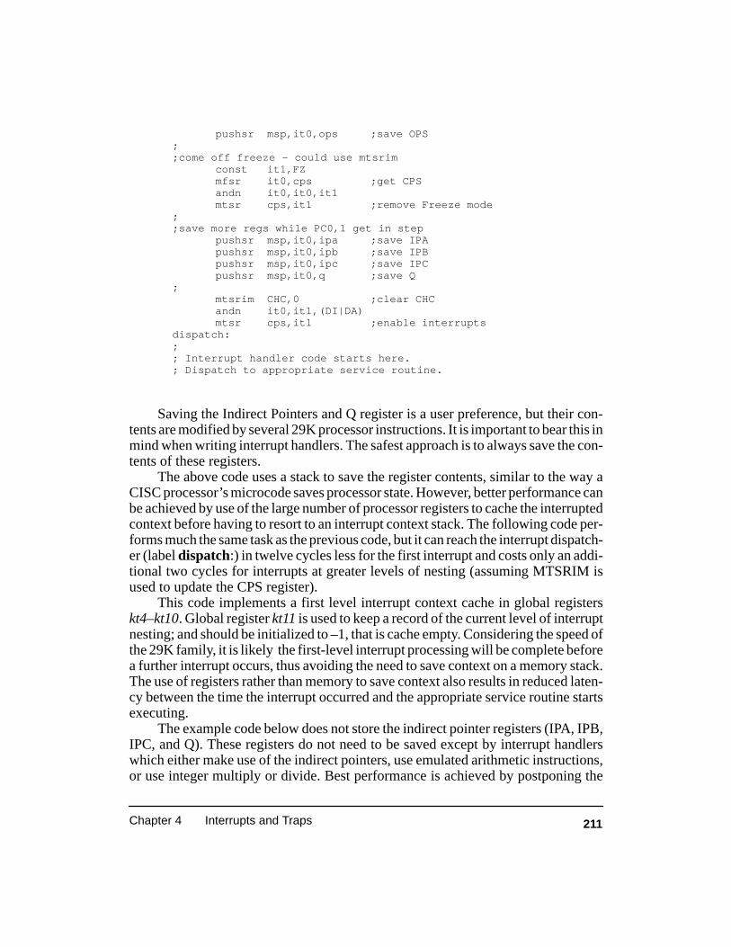
211Chapter 4 Interrupts and Traps
pushsr msp,it0,ops ;save OPS;;come off freeze - could use mtsrim
const it1,FZmfsr it0,cps ;get CPSandn it0,it0,it1mtsr cps,it1 ;remove Freeze mode
;;save more regs while PC0,1 get in step
pushsr msp,it0,ipa ;save IPApushsr msp,it0,ipb ;save IPBpushsr msp,it0,ipc ;save IPCpushsr msp,it0,q ;save Q
;mtsrim CHC,0 ;clear CHCandn it0,it1,(DI|DA)mtsr cps,it1 ;enable interrupts
dispatch:;; Interrupt handler code starts here.; Dispatch to appropriate service routine.
Saving the Indirect Pointers and Q register is a user preference, but their con-tents are modified by several 29K processor instructions. It is important to bear this inmind when writing interrupt handlers. The safest approach is to always save the con-tents of these registers.
The above code uses a stack to save the register contents, similar to the way aCISC processor’s microcode saves processor state. However, better performance canbe achieved by use of the large number of processor registers to cache the interruptedcontext before having to resort to an interrupt context stack. The following code per-forms much the same task as the previous code, but it can reach the interrupt dispatch-er (label dispatch:) in twelve cycles less for the first interrupt and costs only an addi-tional two cycles for interrupts at greater levels of nesting (assuming MTSRIM isused to update the CPS register).
This code implements a first level interrupt context cache in global registerskt4–kt10. Global register kt11 is used to keep a record of the current level of interruptnesting; and should be initialized to –1, that is cache empty. Considering the speed ofthe 29K family, it is likely the first-level interrupt processing will be complete beforea further interrupt occurs, thus avoiding the need to save context on a memory stack.The use of registers rather than memory to save context also results in reduced laten-cy between the time the interrupt occurred and the appropriate service routine startsexecuting.
The example code below does not store the indirect pointer registers (IPA, IPB,IPC, and Q). These registers do not need to be saved except by interrupt handlerswhich either make use of the indirect pointers, use emulated arithmetic instructions,or use integer multiply or divide. Best performance is achieved by postponing the

212 Evaluating and Programming the 29K RISC Family
saving of these registers to the specific handler routine which expects to use them.Correspondingly, a handler which uses them is also responsible for restoring them.
.equ Kmode,(PD|PI|SM|IM)
not_1st: ;save on stackpushsr msp,it0,pc0 ;save PC0pushsr msp,it0,pc1 ;save PC1pushsr msp,it0,alu ;save ALUpushsr msp,it0,cha ;save CHApushsr msp,it0,chd ;save CHDpushsr msp,it0,chc ;save CHCpushsr msp,it0,ops ;save OPSjmp dispatch–8 mtsrim cps,REMOVE ;remove Freeze mode
intr0: ;save registersjmpf kt11,not_1st ;test cache in use add kt11,kt11,1 ;level count
;cache: ;save in cache
mfsr kt4,pc0 ;save PC0mfsr kt5,pc1 ;save PC1mtsrim cps,REMOVE ;remove Freeze modemfsr kt6,alu ;save ALUmfsr kt7,cha ;save CHAmfsr kt8,chd ;save CHDmfsr kt9,chc ;save CHCmfsr kt10,ops ;save OPS
;mtsrim chc,0 ;clear CHCmtsrim cps,Kmode ;enable interrupts
;dispatch:;; Interrupt handler code starts here.; Dispatch to appropriate handler.
4.3.10 Enabling Interrupts
Interrupts are enabled by clearing the DI and DA bits of the CPS. If an un-masked interrupt, INTR[0..3], is pending at this point (the IP bit of the CPS register isset to 1), the processor will immediately process the interrupt and execute the handlerat the new vector address.
In the previous code example, when interrupts are enabled, and if an interruptoccurs, the succeeding register saves will not be performed; however, the recentlyinvoked interrupt handler will save these registers if it intends to enable interruptsduring its execution. The contents of the Indirect Pointers and Q register will be pre-served, or not touched, depending on the nature of the nested interrupt handler.
When clearing the DI and DA bits of the CPS register, the state of the other bitsmust be saved. The first example code illustrates this by using an ANDN instruction

213Chapter 4 Interrupts and Traps
to AND the c urrent contents of the register, with a complement bit pattern of the DAand DI bits in that register (i.e., 11111111 1111 1100).
Figure 4-4 shows the interrupt enable logic of the Am29000 processor. Noticethat interrupts generated by the on-chip timer are controlled by the DA bit in the CPSregister. This indicates it is impossible to enable traps for use by ASSERT and otherinstructions, without also permitting asynchronous interrupts from the timer to occur(unless the on-chip timer is not being used). If it is necessary to avoid timer interrupts,the IE bit in the TMR register can be saved, then cleared to disable timer interrupts.
The interrupt inputs to the Prioritizer logic (as shown in Figure 4-4) are notlatched, and must be continuously asserted by an interrupting external device untilthe interrupt has been recognized. Recognition of the interrupt is usually accom-plished by executing an instruction that accesses the interrupting device. This re-moves the interrupt request, which must be done before interrupts are enabled; other-wise, the same interrupt will recur immediately when interrupts are enabled.
The Interrupt Mask (IM) field of the CPS register can be used to disable recogni-tion of interrupt requests on the INTR inputs. The mask bits implement a simplifiedinterrupt priority scheme that can be set up to recognize only higher-priority inter-rupts, while another handler is in execution.
The two-bit IM field allows four priority levels to be established. An IM fieldvalue of zero (IM=00) enables only the interrupts occurring at the INTR0 input.When IM = 01, both INTR0 and INTR1 are enabled; if IM = 10, then INTR0, INTR1,and INTR2 are enabled; and if IM = 11, then INTR0, INTR1, INTR2, and INTR3 are
DA
Instruction Access Exception
Data Access Exception
Coprocessor ExceptionInterruptRequest
OR AND
Traps 0–1
Internal Traps
Timer
DI
IM
PrioritiserINTs0–3
IE
AND
ANDOR
Figure 4-4. Am29000 Processor Interrupt Enable Logic
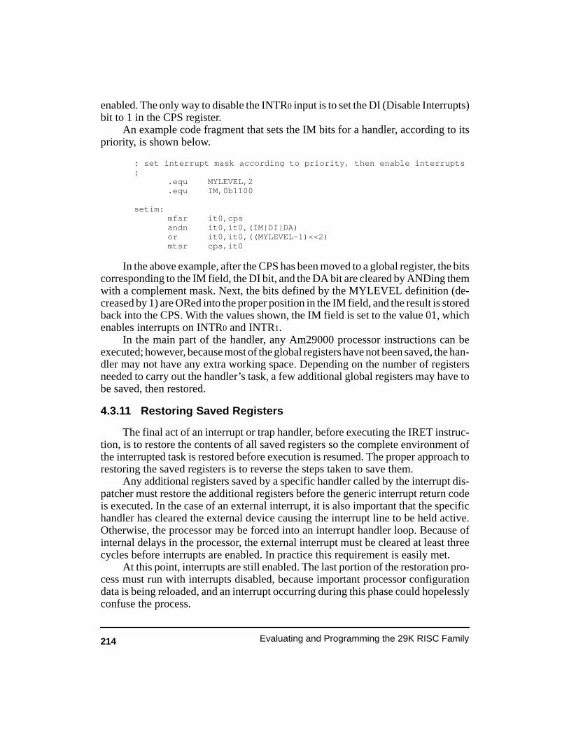
214 Evaluating and Programming the 29K RISC Family
enabled. The only way to disable the INTR0 input is to set the DI (Disable Interrupts)bit to 1 in the CPS register.
An example code fragment that sets the IM bits for a handler, according to itspriority, is shown below.
; set interrupt mask according to priority, then enable interrupts;
.equ MYLEVEL,2
.equ IM,0b1100
setim:mfsr it0,cpsandn it0,it0,(IM|DI|DA)or it0,it0,((MYLEVEL-1)<<2)mtsr cps,it0
In the above example, after the CPS has been moved to a global register, the bitscorresponding to the IM field, the DI bit, and the DA bit are cleared by ANDing themwith a complement mask. Next, the bits defined by the MYLEVEL definition (de-creased by 1) are ORed into the proper position in the IM field, and the result is storedback into the CPS. With the values shown, the IM field is set to the value 01, whichenables interrupts on INTR0 and INTR1.
In the main part of the handler, any Am29000 processor instructions can beexecuted; however, because most of the global registers have not been saved, the han-dler may not have any extra working space. Depending on the number of registersneeded to carry out the handler’s task, a few additional global registers may have tobe saved, then restored.
4.3.11 Restoring Saved Registers
The final act of an interrupt or trap handler, before executing the IRET instruc-tion, is to restore the contents of all saved registers so the complete environment ofthe interrupted task is restored before execution is resumed. The proper approach torestoring the saved registers is to reverse the steps taken to save them.
Any additional registers saved by a specific handler called by the interrupt dis-patcher must restore the additional registers before the generic interrupt return codeis executed. In the case of an external interrupt, it is also important that the specifichandler has cleared the external device causing the interrupt line to be held active.Otherwise, the processor may be forced into an interrupt handler loop. Because ofinternal delays in the processor, the external interrupt must be cleared at least threecycles before interrupts are enabled. In practice this requirement is easily met.
At this point, interrupts are still enabled. The last portion of the restoration pro-cess must run with interrupts disabled, because important processor configurationdata is being reloaded, and an interrupt occurring during this phase could hopelesslyconfuse the process.
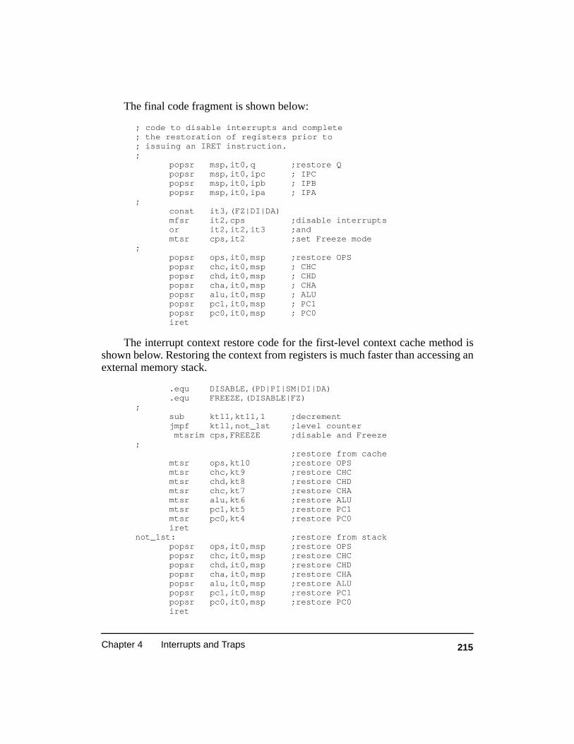
215Chapter 4 Interrupts and Traps
The final code fragment is shown below:
; code to disable interrupts and complete; the restoration of registers prior to; issuing an IRET instruction.;
popsr msp,it0,q ;restore Qpopsr msp,it0,ipc ; IPCpopsr msp,it0,ipb ; IPBpopsr msp,it0,ipa ; IPA
;const it3,(FZ|DI|DA)mfsr it2,cps ;disable interruptsor it2,it2,it3 ;andmtsr cps,it2 ;set Freeze mode
;popsr ops,it0,msp ;restore OPSpopsr chc,it0,msp ; CHCpopsr chd,it0,msp ; CHDpopsr cha,it0,msp ; CHApopsr alu,it0,msp ; ALUpopsr pc1,it0,msp ; PC1popsr pc0,it0,msp ; PC0iret
The interrupt context restore code for the first-level context cache method isshown below. Restoring the context from registers is much faster than accessing anexternal memory stack.
.equ DISABLE,(PD|PI|SM|DI|DA)
.equ FREEZE,(DISABLE|FZ);
sub kt11,kt11,1 ;decrementjmpf kt11,not_1st ;level counter mtsrim cps,FREEZE ;disable and Freeze
;;restore from cache
mtsr ops,kt10 ;restore OPSmtsr chc,kt9 ;restore CHCmtsr chd,kt8 ;restore CHDmtsr chc,kt7 ;restore CHAmtsr alu,kt6 ;restore ALUmtsr pc1,kt5 ;restore PC1mtsr pc0,kt4 ;restore PC0iret
not_1st: ;restore from stackpopsr ops,it0,msp ;restore OPSpopsr chc,it0,msp ;restore CHCpopsr chd,it0,msp ;restore CHDpopsr cha,it0,msp ;restore CHApopsr alu,it0,msp ;restore ALUpopsr pc1,it0,msp ;restore PC1popsr pc0,it0,msp ;restore PC0iret
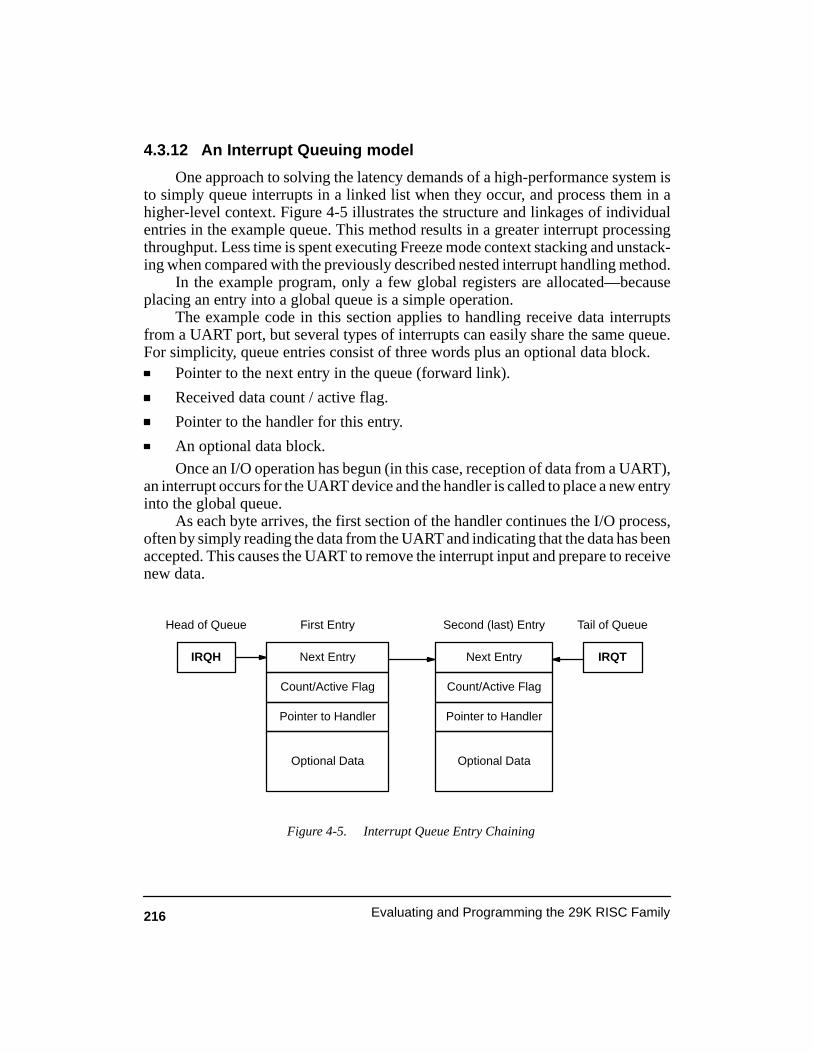
216 Evaluating and Programming the 29K RISC Family
4.3.12 An Interrupt Queuing model
One approach to solving the latency demands of a high-performance system isto simply queue interrupts in a linked list when they occur, and process them in ahigher-level context. Figure 4-5 illustrates the structure and linkages of individualentries in the example queue. This method results in a greater interrupt processingthroughput. Less time is spent executing Freeze mode context stacking and unstack-ing when compared with the previously described nested interrupt handling method.
In the example program, only a few global registers are allocated—becauseplacing an entry into a global queue is a simple operation.
The example code in this section applies to handling receive data interruptsfrom a UART port, but several types of interrupts can easily share the same queue.For simplicity, queue entries consist of three words plus an optional data block.
Pointer to the next entry in the queue (forward link).
Received data count / active flag.
Pointer to the handler for this entry.
An optional data block.
Once an I/O operation has begun (in this case, reception of data from a UART),an interrupt occurs for the UART device and the handler is called to place a new entryinto the global queue.
As each byte arrives, the first section of the handler continues the I/O process,often by simply reading the data from the UART and indicating that the data has beenaccepted. This causes the UART to remove the interrupt input and prepare to receivenew data.
IRQTIRQH Next Entry
Count/Active Flag
Pointer to Handler
Optional Data
Next Entry
Head of Queue Tail of QueueFirst Entry Second (last) Entry
Figure 4-5. Interrupt Queue Entry Chaining
Count/Active Flag
Pointer to Handler
Optional Data

217Chapter 4 Interrupts and Traps
Only one receive operation for a given interrupt can be in progress at a time. Thisallows the queue entry to contain three things: a static entry descriptor that holds apointer to the next entry in the queue, the byte count, and a pointer to the high-levelhandler function.
The example shown below uses four global (interrupt temporary) registers forits queue building processes. Because interrupts are disabled during this entire part ofthe process, handlers for other interrupts can use these same registers.
After the first byte has been stored in the static buffer, the handler must deter-mine if the queue is empty or if it already contains one or more entries. If empty, thehandler can immediately invoke a routine to process the entry. If the queue containsone or more entries, the current entry is linked into the queue. The code is shown be-low.
; UART receive interrupt handler (intr0);
.reg irqh,gr80 ;queue head pointer
.reg irqt,gr81 ;queue tail pointer
.dataentry:
.word 0,0,receive ;entry descriptor
.block 256 ; and data block
intr0:const it1,entry+4 ;address of entryconsth it1,entry+4load 0,0,it0,it1 ;get countadd it3,it1,8 ;address of dataadd it3,it3,it0 ;add countadd it0,it0,4 ;increment countstore 0,0,it0,it1 ;count->entry+4const it2,uart_rcv ;UART data addressconsth it2,uart_rcvload 0,1,it2,it2 ;get data from UARTstore 0,1,it2,it3 ;save in buffer
cpeq it0,it0,4 ;first byte?jmpt it0,startup ;yes, start daemon nopiret ;no, return
startup: ;go daemon if not already runningcpeq it2,irqh,0 ;is queue emptyjmpf it2,add ;no, link this entry sub it1,it1,4 ;point to entryjmp daemon ;yes, go daemon add irqh,it1,0 ;init queue header
add:store 0,0,it1,irqt ;tail->entry
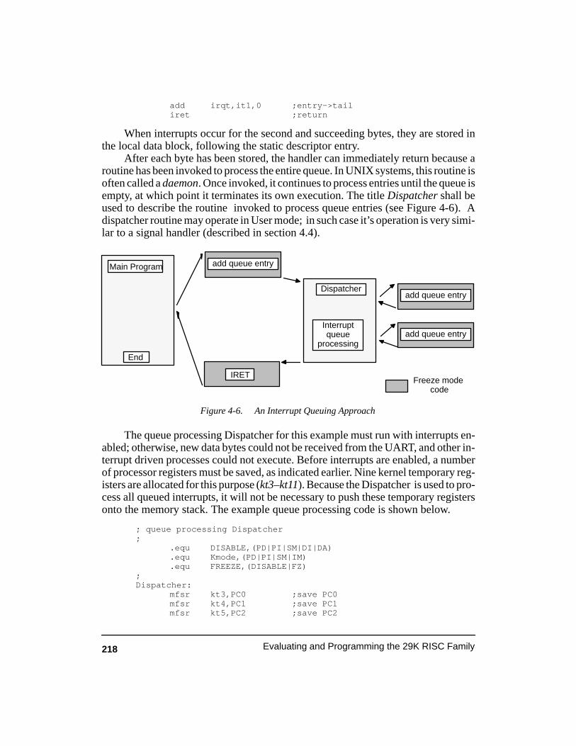
218 Evaluating and Programming the 29K RISC Family
add irqt,it1,0 ;entry->tailiret ;return
When interrupts occur for the second and succeeding bytes, they are stored inthe local data block, following the static descriptor entry.
After each byte has been stored, the handler can immediately return because aroutine has been invoked to process the entire queue. In UNIX systems, this routine isoften called a daemon. Once invoked, it continues to process entries until the queue isempty, at which point it terminates its own execution. The title Dispatcher shall beused to describe the routine invoked to process queue entries (see Figure 4-6). Adispatcher routine may operate in User mode; in such case it’s operation is very simi-lar to a signal handler (described in section 4.4).
End
Main Program
IRET
Figure 4-6. An Interrupt Queuing Approach
Freeze mode code
Interruptqueue
processing
add queue entry
Dispatcheradd queue entry
add queue entry
The queue processing Dispatcher for this example must run with interrupts en-abled; otherwise, new data bytes could not be received from the UART, and other in-terrupt driven processes could not execute. Before interrupts are enabled, a numberof processor registers must be saved, as indicated earlier. Nine kernel temporary reg-isters are allocated for this purpose (kt3–kt11). Because the Dispatcher is used to pro-cess all queued interrupts, it will not be necessary to push these temporary registersonto the memory stack. The example queue processing code is shown below.
; queue processing Dispatcher;
.equ DISABLE,(PD|PI|SM|DI|DA)
.equ Kmode,(PD|PI|SM|IM)
.equ FREEZE,(DISABLE|FZ);Dispatcher:
mfsr kt3,PC0 ;save PC0mfsr kt4,PC1 ;save PC1mfsr kt5,PC2 ;save PC2
219Chapter 4 Interrupts and Traps
mfsr kt6,CHA ;save CHAmfsr kt7,CHD ;save CHDmfsr kt8,CHC ;save CHCmfsr kt9,ALU ;save ALUmfsr kt10,OPS ;save OPSmtsrim CPS,DISABLE ;remove Freeze modemtsrim CHC,0 ;clear CHCadd irqt,irqh,0 ;set tail = head
loop:mtsrim CPS,Kmode ;enable interruptsadd kt11,irqh,8 ;point to handlerload 0,0,kt11,kt11 ;get addresscalli kt11,kt11 ;call handler nopmtsrim CPS,DISABLE ;disable interrupts
cpeq kt11,irqt,irqh ;queue empty?jmpt kt11,finish ;yes, wrapup nopload 0,0,kt11,irqh ;no, get next entryjmp loop ;and loop back add irqh,kt11,0 ;with head<-next
finish:mtsrim cps,FREEZE ;enable freeze modeconst irqh,0 ;make queue emptymtsr PC0,kt3 ;restore PC0mtsr PC1,kt4 ;restore PC1mtsr PC2,kt5 ;restore PC2mtsr CHA,kt6 ;restore CHAmtsr CHD,kt7 ;restore CHDmtsr CHC,kt8 ;restore CHCmtsr ALU,kt9 ;restore ALUmtsr OPS,kt10 ;restore OPSiret ;terminate execution
Note that the example code does not save the Indirect Pointers (IPA–IPC) or theQ register. If any of the individual high-level handlers will disturb the contents ofthese registers, they must also be saved. If high-level handlers are written carefully, itwill not be necessary to save.
The queue processor is responsible for removing entries from the queue andcalling the handler associated with each entry. In the above example, a pointer to thehigh level handler is contained in the third word of the entry descriptor (in this case,receive).
The handler is called after Freeze mode has been disabled, and interrupts are en-abled. When the handler receives control, the IRQH register points to the queue entry.
The high-level handler is responsible for removing the data associated with aqueue entry, and it must do this with interrupts disabled; however, interrupts needonly be disabled while the data is being removed and when the queue entry data count
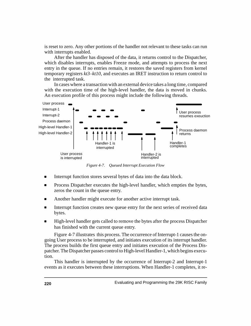
220 Evaluating and Programming the 29K RISC Family
is reset to zero. Any other portions of the handler not relevant to these tasks can runwith interrupts enabled.
After the handler has disposed of the data, it returns control to the Dispatcher,which disables interrupts, enables Freeze mode, and attempts to process the nextentry in the queue. If no entries remain, it restores the saved registers from kerneltemporary registers kt3–kt10, and executes an IRET instruction to return control tothe interrupted task.
In cases where a transaction with an external device takes a long time, comparedwith the execution time of the high-level handler, the data is moved in chunks.An execution profile of this process might include the following threads.
Interrupt-1
Process daemon
Interrupt-2
High-level Handler-1
High-level Handler-2
Handler-1 isinterrupted
interrupted
Handler-1completes
Process daemon
Figure 4-7. Queued Interrupt Execution Flow
User process
User processis interrupted
User process resumes exeuction
Handler-2 is
returns
Interrupt function stores several bytes of data into the data block.
Process Dispatcher executes the high-level handler, which empties the bytes,zeros the count in the queue entry.
Another handler might execute for another active interrupt task.
Interrupt function creates new queue entry for the next series of received databytes.
High-level handler gets called to remove the bytes after the process Dispatcherhas finished with the current queue entry.
Figure 4-7 illustrates this process. The occurrence of Interrupt-1 causes the on-going User process to be interrupted, and initiates execution of its interrupt handler.The process builds the first queue entry and initiates execution of the Process Dis-patcher. The Dispatcher passes control to High-level Handler-1, which begins execu-tion.
This handler is interrupted by the occurrence of Interrupt-2 and Interrupt-1events as it executes between these interruptions. When Handler-1 completes, it re-

221Chapter 4 Interrupts and Traps
turns control to the Process Dispatcher, which selects the next queue entry and turnscontrol over to high-level Handler-2.
During this execution, one more Interrupt-1 event occurs, which results in thecreation of another queue entry. This entry is processed when high-level Handler-2finishes its execution and the Process Dispatcher again receives control.
High-level Handler-1 processes the remaining data and returns control to theProcess Dispatcher which, upon finding no more queue entries, returns to the inter-rupted user process.
Each execution of the interrupt processes Interrupt-1 or Interrupt-2, as well asthe Process Dispatcher and high-level Handler-1 and high-level Handler-2 code seg-ments, is quite short; however, with the short execution approach, individual inter-rupt priorities are not taken into account. If priority handling of interrupts is impor-tant, a different approach is needed. For example, entries could be linked into a singlequeue, with their position in the queue determined by their priority. In this case, moresophisticated queue handling procedures would have to be implemented; however, agiven high-level handler would still execute to completion before another handler isgiven control.
To handle fully-nested priority-oriented interrupts, that is the ability of a higherpriority interrupt to preempt the execution of a lower priority handler, requiresan interrupt stack (possibly with the support of a interrupt context cache). It is ques-tionable whether the responsiveness of the nested interrupt technique would overridethe increased overhead of saving and restoring many sets of registers.
In the approach shown in the previous code only nine global registers are re-quired. These serve for all interrupt handlers in the system. During the executionof the Freeze-mode interrupt handler only four interrupt temporary registers are used(it0–it3).
4.3.13 Making Timer Interrupts Synchronous
The 29K on–chip timer can be configured to generate an interrupt when theTimer Counter Register (TCR) decrements to zero; more accurately, when the 24–bitTCV field of the TCV register reaches zero. The TCV field is decremented with eachprocessor cycle; when it reaches zero, it is loaded with the Timer Reload Value field(TRV) in the Timer Reload register (TR).
When the Interrupt Enable bit (IE) of the TR register is set and the TCV reacheszero, the processor will take a timer interrupt unless the DA bit is set in the Configu-ration Register (CFG). Two–bus and microcontroller members of the 29K family canadditionally disable timer interrupts by setting the TD bits in the CPS register. Timerinterrupts are not disabled by setting the DI bit in the CFG. This means timer inter-rupts can not be simply disabled along with other external asynchronous interruptsby setting DI. Note, the TRAP[1,0] asynchronous inputs are not disabled by setting
222 Evaluating and Programming the 29K RISC Family
the DI bit. For this reason, the use of TRAP[1,0] pins requires complex software sup-port. It is best to avoid the use of these input pins.
It is often desirable to disable timer interrupts during critical code stages, be-cause timer interrupts often lead to such tasks as context switching. However, timerinterrupts may be required to support a real–time clock, and to maintain accuracy, atimer interrupt can not be missed. The timer interrupt must be taken but processingthe event can be postponed till later, when it can be dealt with. To do this efficiently,the Freeze mode interrupt handler for the timer should set register ast to true. Thisregister is a kernel space support register chosen from the range ks0–ks15(gr80–gr95). It indicates an Asynchronous Software Trap (AST) is ready for proces-sing. The ast register can be quickly tested with an ASSERT type instruction, asshown below:
mfsr it0,ops ;get OPS register, DA already clearandn it0,it0,1 ;clear DI bitmtsrim ops,it0 ;enable interruptsasneq V_AST,ast,0 ;trap if ast != 0, timer ’event’iret ;otherwise iret
Clearing the DI bit reenables asynchronous interrupts (with the exception thatTRAP[1,0] are already active); but we must check to see if an AST is pending (timerevent). The high level timer processing is performed before the IRET instruction isexecuted, via trapware supporting the V_AST trap.
4.4 USER-MODE INTERRUPT HANDLERS
Many present day operating systems allow interrupt handlers to be written inhigh-order languages. User mode routines for 29K Processor Family based systemsare no different. When providing this facility, the operating system designer must beaware of the following concerns.
User mode programs are often written by programmers who lack specificknowledge of the operating system and it’s allocation of global registers.
The User mode handler, when written in a high-level language, such as C, willrequire access to the local register stack, as well as global registers defined forits management.A good approach for addressing these concerns is to perform all necessary regis-
ter saving, with interrupts disabled, while in Supervisor mode; remove the cause ofthe interrupt, then enable interrupts and enter User mode to execute the user’s inter-rupt handler code. This allows interrupt (signal) handlers to be compatible withAMD’s Host Interface (HIF) v2.0 Specification (see section 2.2), which includes thedefinition of operating system services . These services install and invoke user-sup-plied interrupt handlers for floating-point exceptions and keyboard interrupt

223Chapter 4 Interrupts and Traps
(SIGFPE and SIGINT) events. It also allows the operating system to perform its ownregister preservation and restoration processes, without burdening the user with tech-nical operating system details. Complete listings of the code contained in this sectionare provided in Appendix B and also by AMD in their library source code. Users whointend to modify any of this code should bear in mind that the SPILL , FILL , setjmp,longjmp, and Signal Trampoline code are highly interdependent.
The code uses an expanded interface definition that uses a set of global registersto hold the important local register stack support values emitted by compiler gener-ated code in User mode programs. The registers defined for this environment areshown in Table 4-2, and were discussed in detail in section 3.3 (page 117).
Table 4-2. Expanded Register Usage
Names RegistersUsage Description
tav gr121 Trap Argument Vectortpc gr122 Trap Return Pointerlrp gr123 Large Return Pointerslp gr124 Static Link Pointermsp gr125 Memory Stack Pointerrab gr126 Register Allocate Boundrfb gr127 Register Free Bound
In order to prepare for execution of a User mode handler, the HIF specificationindicates that the Supervisor mode portion of the handler must save important regis-ters in the user’s memory stack, as shown in Figure 4-8. In the figure, the stack point-er (msp) is shown decremented by 48 bytes (12 registers times 4 bytes each), andpositioned to point to the saved value of register tav.
Other registers may need to be saved to allow complete freedom in executing29K processor instructions (such as multiply or divide trap routines) in the User-mode handler code. Candidates for saving are the Indirect Pointers (IPA–IPC), the Qregister, the stack frame pointer, fp (lr1), and the local register stack bounds in rfb. Inaddition, because high-level languages use many of the global registers as tempo-raries, these (gr96–gr124) may also have to be saved.
4.4.1 Supervisor mode Code
When an interrupt occurs, the supervisor portion of the interrupt handler isexecuted. This code is responsible for saving important processor registers, as shownin Figure 4-8. The assembler macro instructions, used earlier in this chapter (push,pop, pushsr and popsr), and described in detail in section 3.3.1 (page 119), are used inthe following code examples to aid in pushing special registers onto the memorystack.
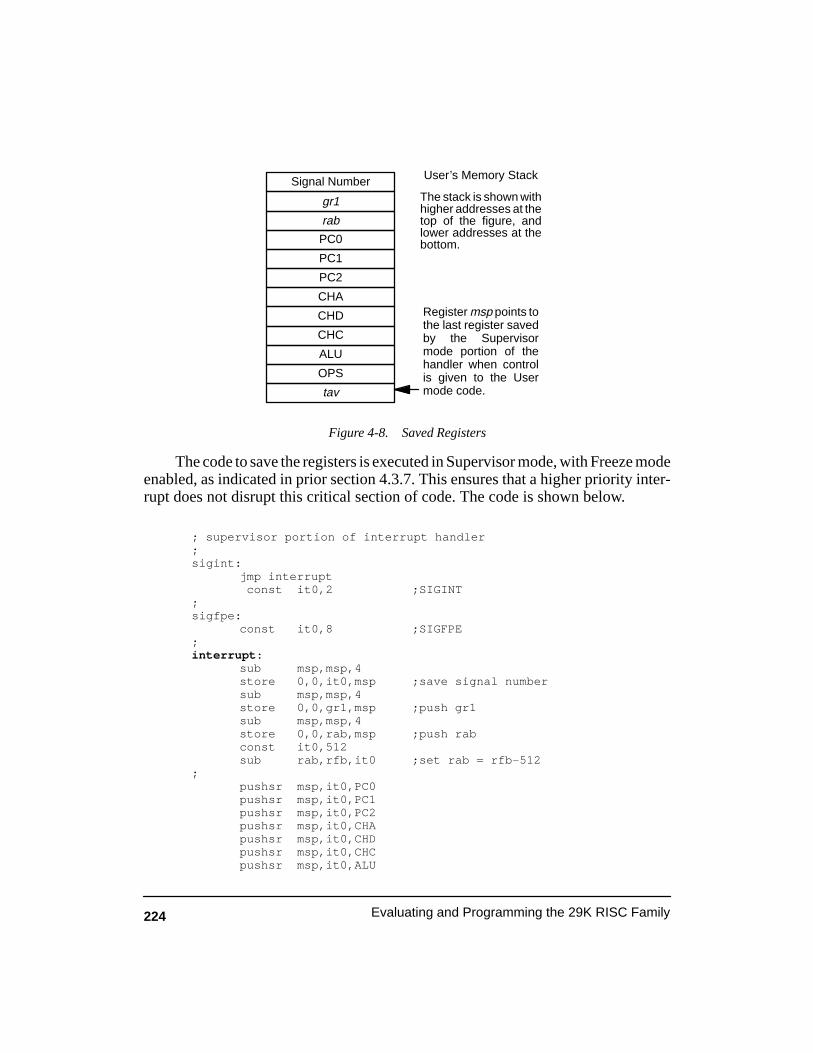
224 Evaluating and Programming the 29K RISC Family
Signal Number
PC0
PC1
PC2
CHA
CHD
CHC
ALU
OPS
tav
User’s Memory Stack
Figure 4-8. Saved Registers
Register msp points tothe last register savedby the Supervisormode portion of thehandler when controlis given to the Usermode code.
The stack is shown withhigher addresses at thetop of the figure, andlower addresses at thebottom.
gr1
rab
The code to save the registers is executed in Supervisor mode, with Freeze modeenabled, as indicated in prior section 4.3.7. This ensures that a higher priority inter-rupt does not disrupt this critical section of code. The code is shown below.
; supervisor portion of interrupt handler;sigint:
jmp interrupt const it0,2 ;SIGINT
;sigfpe:
const it0,8 ;SIGFPE;interrupt :
sub msp,msp,4store 0,0,it0,msp ;save signal numbersub msp,msp,4store 0,0,gr1,msp ;push gr1sub msp,msp,4store 0,0,rab,msp ;push rabconst it0,512sub rab,rfb,it0 ;set rab = rfb-512
;pushsr msp,it0,PC0pushsr msp,it0,PC1pushsr msp,it0,PC2pushsr msp,it0,CHApushsr msp,it0,CHDpushsr msp,it0,CHCpushsr msp,it0,ALU

225Chapter 4 Interrupts and Traps
pushsr msp,it0,OPS;
sub msp,msp,4store 0,0,tav,4 ;push tav
trampoline:
At this point in the code, with all of the critical registers saved, the memory stackwill appear as shown in Figure 4-8. When the User mode interrupt handler is com-plete, these registers will be restored.
Special provisions were made in the code above in anticipation of the followingsituation: If a FILL operation is interrupted, and the trampoline code has not yetrealigned the rab register to rfb-WindowSize, another interrupt occurring at thatpoint could again activate the trampoline code. This interrupt could cause the tram-poline code to assume that a FILL operation was in progress, thereby causing it to“reposition” the value in PC1 to recommence the (assumed) FILL operation.
; Now come off freeze, and go to user -mode code.; ensure load/store does not restart;trampoline : ;ensure load/store
mtsrim chc,0 ; does not restartconst it1,RegSigHandconsth it1,RegSigHandload 0,0,it1,it1cpeq it0,it1,0jmpt it0,SigDfl ;jump if no handler(s) add it0,it1,4mtsr pc1,it1mtsr pc0,it0iret
Two types of interrupts are handled by this code: keyboard interrupts and float-ing-point exceptions. It is assumed that the interrupt vectors were previously set tovector to either sigint or sigfpe, depending on the type of interrupt. Interrupt tempo-rary (it0 ) is used to contain the type of interrupt (signal), when entering the commoncode at label interrupt .
Once the memory stack is set up as indicated, the User mode portion of the han-dler (beginning at label sigcode) is placed into execution by loading Program Count-ers (PC0 and PC1) with the address of the handler. Then while still in Freeze modewith interrupts disabled, an IRET instruction is executed to begin execution of thehandler.
The HIF specification indicates that User mode signal handlers must call one ofthe specified signal return services to return control to the user’s code at the appropri-ate point. When one of these services (sigret, sigrep, sigdfl, or sigskp) is called via anASSERT instruction, msp will point to the same location shown in Figure 4-8, so thesupervisor portion of the handler can properly restore the interrupted task’s environ-ment.

226 Evaluating and Programming the 29K RISC Family
The following code fragment illustrates how one of the return services restoresall of the registers. It is invoked by the HIF Service Trap (69) with interrupts disabledand Freeze mode enabled—as is the case with any interrupt or trap.
; Signal return service, restore registers;sigret:; assume msp points to tav load 0,0,tav,msp ;restore tav
add msp,msp,4;
popsr OPS,it0,msp ;pop specialspopsr ALU,it0,msppopsr CHC,it0,msppopsr CHD,it0,msppopsr CHA,it0,msppopsr PC2,it0,msppopsr PC1,it0,msppopsr PC0,it0,mspload 0,0,rab,msp ;pop rabadd msp,msp,4load 0,0,it0,msp ;pop rspadd gr1,it0,0add msp,msp,8 ;discount signal iret ; number
As indicated in the HIF Specification, User mode interrupt handlers must save anumber of additional registers, to prepare for executing high-level language code.The following section discusses some of the necessary preparations.
4.4.2 Register Stack Operation
The 29K Processor Family contains 128 general registers that can be configuredas a register stack. In this case, global register (gr1) is used to point to the first registerin this group that belongs to the current process. This first register is addressed as lr0(local register 0).
Several additional global registers provide other information describing theregister stack bounds. These are all shown in Figure 4-9, which illustrates the imple-mentation of the local register file as a shadow copy of the memory-based registerstack cache.
The rab, rsp, lr1, and rfb registers (shown in Figure 4-9) contain the bounds ofthe current memory stack cache in the form of addresses.
The rsp (register stack pointer) shown in Figure 4-9 is assigned to global regis-ter gr1, whose low-order 9 bits (bits 0 and 1 are not used for register addressing) areused to address the local register file whenever a local register number is encounteredin a 29K processor instruction. Therefore, local register lr2 is actually referenced bythe CPU, by adding 8 (2 words) to the value held in register gr1.
Other important details of the register stack and local register file are discussedin Chapter 7 (Operating System Issues).
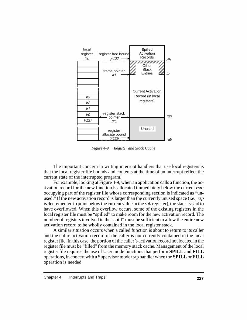
227Chapter 4 Interrupts and Traps
Figure 4-9. Register and Stack Cache
ÍÍÍÍÍÍÍÍÍÍÍÍÍÍÍÍÍÍÍÍÍÍÍÍÍÍÍÍ
SpilledActivationRecords
Current ActivationRecord (in local
registers)
localregister
fileregister free bound
gr127
frame pointerlr1
register stackpointer
gr1
registerallocate bound
gr126
lr3
lr2
lr1
lr0
lr127
rfb
fp
rsp
rab
OtherStack
Entries
Unused
The important concern in writing interrupt handlers that use local registers isthat the local register file bounds and contents at the time of an interrupt reflect thecurrent state of the interrupted program.
For example, looking at Figure 4-9, when an application calls a function, the ac-tivation record for the new function is allocated immediately below the current rsp;occupying part of the register file whose corresponding section is indicated as “un-used.” If the new activation record is larger than the currently unused space (i.e., rspis decremented to point below the current value in the rab register), the stack is said tohave overflowed. When this overflow occurs, some of the existing registers in thelocal register file must be “spilled” to make room for the new activation record. Thenumber of registers involved in the “spill” must be sufficient to allow the entire newactivation record to be wholly contained in the local register stack.
A similar situation occurs when a called function is about to return to its callerand the entire activation record of the caller is not currently contained in the localregister file. In this case, the portion of the caller’s activation record not located in theregister file must be “filled” from the memory stack cache. Management of the localregister file requires the use of User mode functions that perform SPILL and FILLoperations, in concert with a Supervisor mode trap handler when the SPILL or FILLoperation is needed.
228 Evaluating and Programming the 29K RISC Family
4.4.3 SPILL and FILL Trampoline
High-level language compilers automatically generate code that tests for a re-quired SPILL upon entry to a called function, and for a required FILL operation justbefore a called function exits. In either case, the SPILL or FILL is initiated by anASSERT instruction whose assertion fails. This causes the SPILL or FILL trap han-dler to begin its execution in Supervisor mode with special registers frozen.
The Supervisor mode code must initiate execution of the appropriate handler byleaving Supervisor mode, and doing its processing in User mode. Several benefits areobtained from operating SPILL or FILL handlers in User mode. First, the overheadof leaving Freeze mode is avoided, handlers must leave Freeze mode because theyrequire the use of load- and store-multiple instructions. Additionally, FILL andSPILL handlers may require several machine cycles to complete, if they were to op-erate with DA set, a potential interrupt latency problem would result.
The following entry points, SpillTrap and FillTrap are directly invoked bytheir corresponding hardware vectors when the associated ASSERT instructionis executed. The operands SpillAddrReg and FillAddrReg are aliased to kernel stat-ic registers (two of ks0–ks15), which hold the addresses of the User mode SPILL andFILL handlers.
Because the processor’s execution jumps from Supervisor mode to User modein this fashion, the SpillTrap and FillTrap code is called a trampoline. The Spill-Trap and FillTrap trampoline code is shown below.
SpillTrap:;; Preserve the return address in the; designated register
mfsr tpc,PC1;; Fixup PC0 and PC1 to point at the user; designated spill handler
mtsr PC1,SpillAddrRegadd tav,SpillAddrReg,4mtsr PC0,tav
;; And return to that handler
iret
FillTrap:;; Preserve the return address in the; designated register
mfsr tpc,PC1;; Fixup PC0 and PC1 to point at the user; designated fill handler

229Chapter 4 Interrupts and Traps
mtsr PC1,FillAddrRegadd tav,FillAddrReg,4mtsr PC0,tav
;; And return to that handler
iret
The SpillTrap and FillTrap routines both turn control over to the User modesections of their respective handlers by modifying the addresses held in the proces-sor’s frozen PC0 and PC1 registers. This happens after the current address in PC1 hasbeen temporarily saved in register tpc (gr122).
When the IRET instruction is executed, the processor reenters User mode, withthe same interrupt enable state as when the trap occurred, and begins execution at theaddress loaded into PC1.
4.4.4 SPILL Handler
The FILL and SPILL handlers are executed in User mode to ensure the greatestprocessor performance for these operations. The handlers are invoked by the Super-visor mode trap handler, usually with interrupts enabled. This permits SPILL andFILL operations to be interrupted, and to use load- and store-multiple operations toaccomplish their task.
An example User mode SPILL handler is shown below.
; spill handler;; spill registers from (*gr1-*rab); and move rab down to where gr1 points.;; On entry: rfb - rab = windowsize,; gr1 < rab.;; Near the end: rfb - rab > windowsize,; gr1 == rab
; On exit: rfb - rab = windowsize,; gr1 == rab;
.global spill_handler
spill_handler:sub tav,rab,gr1 ;bytes to spillsrl tav,tav,2 ;bytes to wordssub tav,tav,1 ;make zero basedmtsr CR,tav ;set CR registersub tav,rab,gr1sub tav,rfb,tav ;dec. rfb by tavadd rab,gr1,0 ;copy rsp into rabstorem 0,0,lr0,tav ;store lr0..lr(tav)jmpi tpc ;return... add rfb,tav,0
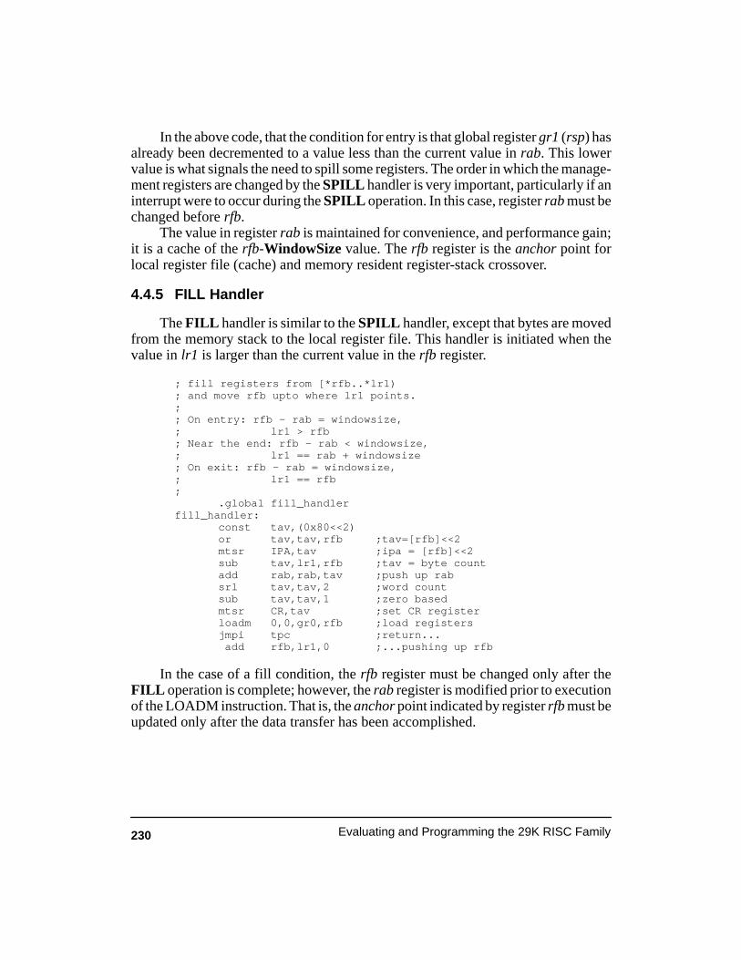
230 Evaluating and Programming the 29K RISC Family
In the above code, that the condition for entry is that global register gr1 (rsp) hasalready been decremented to a value less than the current value in rab. This lowervalue is what signals the need to spill some registers. The order in which the manage-ment registers are changed by the SPILL handler is very important, particularly if aninterrupt were to occur during the SPILL operation. In this case, register rab must bechanged before rfb.
The value in register rab is maintained for convenience, and performance gain;it is a cache of the rfb-WindowSize value. The rfb register is the anchor point forlocal register file (cache) and memory resident register-stack crossover.
4.4.5 FILL Handler
The FILL handler is similar to the SPILL handler, except that bytes are movedfrom the memory stack to the local register file. This handler is initiated when thevalue in lr1 is larger than the current value in the rfb register.
; fill registers from [*rfb..*lr1); and move rfb upto where lr1 points.;; On entry: rfb - rab = windowsize,; lr1 > rfb; Near the end: rfb - rab < windowsize,; lr1 == rab + windowsize; On exit: rfb - rab = windowsize,; lr1 == rfb;
.global fill_handlerfill_handler:
const tav,(0x80<<2)or tav,tav,rfb ;tav=[rfb]<<2mtsr IPA,tav ;ipa = [rfb]<<2sub tav,lr1,rfb ;tav = byte countadd rab,rab,tav ;push up rabsrl tav,tav,2 ;word countsub tav,tav,1 ;zero basedmtsr CR,tav ;set CR registerloadm 0,0,gr0,rfb ;load registersjmpi tpc ;return... add rfb,lr1,0 ;...pushing up rfb
In the case of a fill condition, the rfb register must be changed only after theFILL operation is complete; however, the rab register is modified prior to executionof the LOADM instruction. That is, the anchor point indicated by register rfb must beupdated only after the data transfer has been accomplished.

231Chapter 4 Interrupts and Traps
4.4.6 Register File Inconsistencies
The discussion of SPILL and FILL User mode handlers is important whenwriting interrupt routines because a SPILL or FILL may be incomplete at the timethe interrupt occurs. Depending on whether a SPILL or FILL is in progress, the in-terrupt handler must prepare the register stack support registers before attempting topass control to a User mode handler that makes use of the local register file.
Figure 4-10 illustrates a global view of the register stack, as it might appear bothin the local registers and in the memory stack cache at the time of an interrupt. In thiscase, the interrupt occurred during execution of a SPILL operation, probably duringexecution of the STOREM instruction. Therefore, the address in register gr1 has al-ready been decremented in anticipation that the proposed activation record will fit in
Figure 4-10. Stack Upon Interrupt
ÍÍÍÍÍÍÍÍÍÍÍÍÍÍÍÍÍÍÍÍÍÍÍÍ
SpilledActivationRecordslocal
registerfile
register free boundgr127
frame pointerlr1
register gr1used to point
here
register stackpointer
gr1
lr9
lr8
lr7
lr6
lr3
rfb
fp
rsp, rab
OtherStack
Entries
ProposedActivationRecordlr2
lr1
lr0
lr5
lr4 registerallocate bound
gr126
memory stack cachesetjmp refers
to an activationrecord at this pointin the stack cache
Caller’s ActivationRecord (in local
registers)

232 Evaluating and Programming the 29K RISC Family
the local registers. In addition, because a SPILL operation was necessary, the rabregister has also been set equal to gr1 in the SPILL handler.
The interrupt handler must recognize this condition because it must prepare theregister stack for entry into a C language user interrupt function. This will require thestack management registers to be consistent. Repairing stack inconsistencies de-pends on the interrupt handler being able to recognize each unique situation wheresuch an inconsistency could occur. In the case of the C language environment, thereare three situations that must be detected.
The interrupt occurred when a SPILL was in progress, in which case the dis-tance between the values in the rfb and rab registers exceeds the size of the localregister file (referred to as the WindowSize).
The interrupt occurred when a FILL operation was in progress, in which casethe distance between the values in the rfb and rab registers is less than the size ofthe local register file.
The interrupt occurred during a far-longjmp operation (see Figure 4-12a), inwhich case the value (gr1 + 8) — which is the address of local register lr2 on theregister memory stack — is greater than the value in the rfb register.
The following code fragment illustrates a method of recognizing these inconsis-tent stack conditions.
The Supervisor mode portion of the interrupt handler has saved the importantprocessor registers as shown in Figure 4-8. Because the User mode portion of thehandler is intended to execute a C language function, additional registers will need tobe saved. The register stack support registers, indirect pointers (IPA–IPC), as well asglobal registers (gr96–gr124) are pushed onto the memory stack just below the sig-nal context frame.
sigcode :push msp,lr1 ;push R–stack push msp,rfb ; supportpush msp,msp ;M–stack supportsub msp,msp,3*4 ;Floating Point
;pushsr msp,tav,IPA ;User mode specialspushsr msp,tav,IPBpushsr msp,tav,IPCpushsr msp,tav,Q
;sub msp,msp,29*4 ;push gr96–gr124mtsrim cr,29–1storem 0,0,gr96,msp
Additional space on the memory stack is allocated for floating point registers. Ifthe C language signal handler is to make use of floating point resources then the nec-essary critical support registers should be saved. Further discussion of these and an

233Chapter 4 Interrupts and Traps
explanation of the format of the saved context information can be found in Chapter 5(Operating System Issues). After the additional context status has been saved the reg-ister stack condition can then be examined.
;Recognize inconsistent stack conditions
const gr96,WindowSize;get cache sizeconsth gr96,WindowSizeload 0,0,gr96,gr96add gr98,msp,SIGCTX_RABload 0,0,gr98,gr98 ;interrupted rabsub gr97,rfb,gr98 ;rfb–rab <= WScpgeu gr97,gr97,gr96jmpt gr97,nfill ;jmp if spill add gr97,gr1,8 ;or normal stackcpgtu gr97,gr97,rfb ;longjmp testjmpt gr97,nfill ;yes, longjmp case nop ;jmp if gr1+8 > rfb
;;Fixup registers to re–start FILL operation
ifill:add gr96,msp,SIGCTX_RAB+4push gr96,rab ;resave rab=rfb–512const gr98,fill_handler+4consth gr98,fill_handler+4push gr96,gr98 ;resave PC0sub gr98,gr98,4push gr96,gr98 ;resave PC1const gr98,0sub gr96,gr96,3*4 ;point to CHCpush gr96,gr98 ;resave CHC=0
The variable WindowSize is initialized to the size of the local register stack, inbytes, when the library signal function is first called. Referring to Figure 4-10, and tothe code fragment shown above, it is clear that the result of subtracting the saved rabfrom rfb will be larger than the local register stack size. Therefore, the program willhandle the spill (and normal interrupt) cases by jumping to label nfill . The longjmpcase, once detected, is also sent to the nfill label, where the code discriminates be-tween the conditions.
;discriminate between SPILL, longjmp and; normal interruptsnfill:
cpgtu gr96,gr1,rfb ;if gr1 > rfb jmpt gr96,lower ;then gr1 = rfb cpltu gr96,gr1,rab ;if gr1 < rabjmpt gr96,raise ;then gr1 = rab nop
sendsig:
In the interrupted FILL case, the saved rab value is over-written with the re-aligned rab value. The send-signal code (section 4.4.1) subtracted the WindowSize

234 Evaluating and Programming the 29K RISC Family
from the value in rfb to determine the aligned rab value. This was done before issuingan IRET to sigcode.
Essentially, this restores rab to where it pointed immediately before executingthe function call that caused the FILL operation. Note that this recomputation is alsovalid for a normal case, where the management registers are consistent.
The two comparisons shown below determine which method, if any, should beused to repair the value in register gr1. The method depends on whether a longjmp,SPILL , or normal interrupt occurred. This is required to align gr1 to a valid cacheposition where longjmp or SPILL is interrupted. The following code fragmentshows the code associated with the lower and raise labels.
;lower or raise value in gr1
lower:jmp sendsig add gr1,rfb,0 ;set gr1 = rfb
raise:jmp sendsig add gr1,rab,0 ;set gr1 = rab
According to the situation depicted in Figure 4-10, when a SPILL operation isinterrupted, code at the raise label is executed; however, the code resumes at the labelsendsig.
The code fragment titled “fix–up registers to restart FILL operation”, shownabove, is entered if the interrupt occurred during a FILL operation. If so, it is neces-sary to change the saved values for the Program Counters, PC0 and PC1, and clear thevalue saved in the CHC register. These registers are assumed to have been saved inthe order shown in Figure 4-8. This is required in addition to realigning the registerstack support register, rab.
The identifiers called SIGCTX_RAB, and SIGCTX_SIG are defined as numer-ic offsets (to be added) to the memory stack address held in register msp. Makingthese changes will effectively restart the FILL operation from its beginning. Thiscode also falls into the code beginning at label nfill , but in the case of an interruptedFILL operation, the value in register gr1 will not be adjusted.
4.4.7 Preparing the C Environment
After stack repairs have been made to the (possibly inconsistent) managementregisters, it is necessary to prepare for C language interrupt handler code execution.These preparations consist mainly of setting up a new stack frame from which theuser’s handler can execute. At this point in the process, the register stack and memorycache appear as shown in Figure 4-11.
The following code fragment picks up at the label sendsig, which is repeated forclarity. The handler is almost ready to pass control to the user’s C language handlercode, but first it must set up a stack frame that looks as though the user’s function was

235Chapter 4 Interrupts and Traps
ÍÍÍÍÍÍÍÍÍÍÍÍÍÍÍÍÍÍÍÍÍ
SpilledActivationRecords
localregister
fileregister free
frame pointerslr1
registerallocate bound
rab
lr3
lr2
lr1
lr0
rfb
fp
rsp, rab
OtherStack
Entries
ProposedHandler
ActivationRecord
memory stack cache
Current ActivationRecord (in local
registers)
bound
registerstack pointer
gr1
Figure 4-11. Stack After Fix–up
called in a normal fashion (rather than being invoked as part of an interrupt handler).This is accomplished in the same way a normal C language function allocates itsstack frame upon entry.
; Create an activation record on the stack; for our handler, so the user code will; operate as though it has been “called”;
.equ RALLOC,4*4 ;space for functionsendsig:
sub gr1,gr1,RALLOCasgeu V_SPILL,gr1,rabadd lr1,rfb,0 ;set lr1 = rfbadd gr97,msp,SIGCTX_SIGload 0,0,lr2,gr97 ;restore sig numbersub gr97,lr2,1 ;get handler indexsll gr97,gr97,2 ;point to addresses
;Handler must not use HIF services other ;than the _sigret() type.const gr96,SigEntryconsth gr96,SigEntryadd gr96,gr96,gr97load 0,0,gr96,gr96 ;registered handler cpeq gr97,gr96,0 jmpt gr97,NoHandler nop
236 Evaluating and Programming the 29K RISC Family
calli lr0,gr96 ;call C–level nop ;signal handler
NoHandler:jmp __sigdfl nop
The user function called by the above code is assumed to be one that has beenpassed to the signal library function to process either SIGINT or SIGFPE interrupts,or both. The SigEntry label in the above code refers to a table of pointers. In the ex-ample, one contains the address of a user signal handler for keyboard interrupts (SI-GINT) and the other points to the handler for floating-point exceptions (SIGFPE). Apointer to the user handler for each of these is installed in the SigEntry table by thesignal library function.
4.4.8 Handling Setjmp and Longjmp
Although not strictly related to interrupt handling, many C language librariescontain a setjmp routine used to record the values of the register and memory stacksupport registers, and an additional longjmp routine that allows a program to jump toa consistent environment saved by a previous call to the setjmp routine.
Figure 4-12 illustrates the location in the stack and memory cache to which thesaved information from a previously executed setjmp call might refer. The saved in-formation (stored in a special record specified in the call to setjmp), contains the val-ues of gr1, msp, lr0, and lr1, as they appear when the call to setjmp was made.
Interrupt handler code must make provisions for a User mode handler to call thelongjmp function from within the code. During the course of executing the longjmp,the values stored in the marker record are loaded into their respective registers. Theprocessor is executing in User mode, with interrupts enabled, so this process might beinterrupted at any point. The interrupt handler code that recognizes stack inconsis-tencies (presented earlier) handles this case by fixing up the management registers, toestablish a consistent stack. When the interrupt handler returns, the longjmp will beproperly completed.
Not all User mode signal handlers will have to contend with the complexitiesintroduced by setjmp and longjmp function calls. In this case, the code presentedearlier can be somewhat simplified; however, because the amount of code devoted tothis potential situation is very small, it is recommended that users provide the addi-tional checks and compensating code.

237Chapter 4 Interrupts and Traps
ÉÉÉÉÉÉÉÉÉÉÉÉÉÉÉ
ÉÉÉÉÉÉÉÉÉÉÉÉÉÉÉÉÉÉÉÉÉÉÉÉ
ÉÉÉÉÉÉÉÉÉÉÉÉÉÉÉ
ÉÉÉÉÉÉÉÉÉ
External Memory External Memory
Fill In
rfb
gr1
Cache at setjmp()
Cache at longjmp() Cache after longjmp()
rfb = lr1 (set)
gr1 = gr1 (set)
lr1 (set)
gr1 (set)
ÉÉÉÉÉÉÉÉÉÉÉÉÉÉÉÉ
ÉÉÉÉÉÉÉÉÉÉÉÉÉÉÉ ÇÇÇ
ÇÇÇÉÉÉÉÉÉÉÉÉÉÉÉ
ÉÉÉÉÉÉrfb
gr1
External Memory
Fill InAlreadyin Cache
External Memory
Cache at longjmp() Cache after longjmp()
Cache at setjmp()
rfb = lr1 (set)
gr1 = gr1 (set)
lr1 (set)
gr1 (set)
(b) Long–Jump to a near Setjmp
Figure 4-12. Long–Jump to Setjmp
(a) Long–Jump to a far Setjm

238 Evaluating and Programming the 29K RISC Family

239
Chapter 5
Operating System Issues
Because application programs make use of operating system services, theoverhead costs associated with typically requested services is of great interest. Withthe performance levels offered by the best RISC implementations, these overheadcosts have become very low. However, the often increased complexity of RISCoperating systems has lead to some confusion about the efficiency of operatingsystem implementations.
This chapter discusses in detail the various forms of context switching whichoccur between operating system and application code. This particular task is one ofthe more complex functions supported by a typical operating system. Also discussedare general issues related to context switching. The large number of registersavailable to application programs may initially suggest that the 29K is not ideal atperforming application context switching. However, there are a number ofoptimizations which, when applied, greatly reduce context save and restore times[Mann 1992a].
The code examples shown make use of a number macros for pushing andpopping special registers to an external memory stack. These macros were presentedin section 3.3.1, Assembly Programming.
Within this chapter, context information will be frequently stored and reloadedfrom a per–task data region known as the Process Control Block (PCB). An operatingsystem register in the range of ks1–ks12 is assumed to point within the PCB stack.The example code assumes that the relevant register known as pcb has already beenassigned the correct memory address value by operating system specific code. Theexample code also uses constants of the form CTX_CHC. These are offsets from thetop of the PCB stack (lower address) to the relevant address containing the desiredregister information (the CHC register in the example). When a memory stack is used

240 Evaluating and Programming the 29K RISC Family
to save the context in place of the PCB data structure, the CTX_ offset constants maystill be used.
5.1 REGISTER CONTEXT
Part of the increased performance of the 29K family comes from using 128internal registers as a register stack cache. The cache holds the top of the run–timestack. Each procedure obtains its necessary register allocation by claiming a regionof the register stack. The register cache does not have to be flushed (spilled) untilthere is insufficient unallocated register space. This happens infrequently. Theregister stack offers greater performance benefits over a data memory cache, due toregister cache triple porting on–chip (two read ports and one write port). Note, theAm29050 has an additional write port which can be used to simultaneouslywrite–back a result from the floating–point unit. Chapter 2 explains in detail theprocedure calling mechanism’s use of the cache.
However, when a context switch is required from one user task to another usertask, it is necessary to copy all internal registers currently allocated to the current usertask to a data memory save region. This makes the registers available for use by thein–coming task.
In performing a context switch, a clear understanding is required of processorregister usage. The AMD C Language register usage convention (see section 2.1)makes 33 of the 65 global registers (gr1, gr96–gr127) available for User data storage.Global registers gr128–gr255, used to implement the local register stack, are alsoused by the compiler generated code. (See section 3.3 (page 117) of Chapter 3,Assembly Language Programming, for global register assignment.)
Processor global registers gr64–gr95 are not accessed by C generated code.These registers are normally used by the Supervisor to store operating systeminformation or implement interrupt handler temporary working space. ParticularSupervisor implementations may store data in registers gr64–gr95. This data isrelevant to the task currently executing, and includes such information as pointers tomemory resident data structures containing system support information. This datamay also have to be copied–out to memory when a task switch is required.
The C procedure calling convention specifies that global registers gr96–gr111are used for return value passing. For a procedure returning a 32–bit integer, onlyregister gr96 is required to store return value information. The compiler generallyuses these global registers for temporary working space before the return value datais determined. The compiler has nine more temporary registers in the gr112–gr127range which can also be used for temporary data storage. Other registers in this rangeare used to implement register stack support functions.
When more registers are required by a procedure for data storage, the localregister stack can be used. This reduces the need to use external data memory to storeprocedure data.
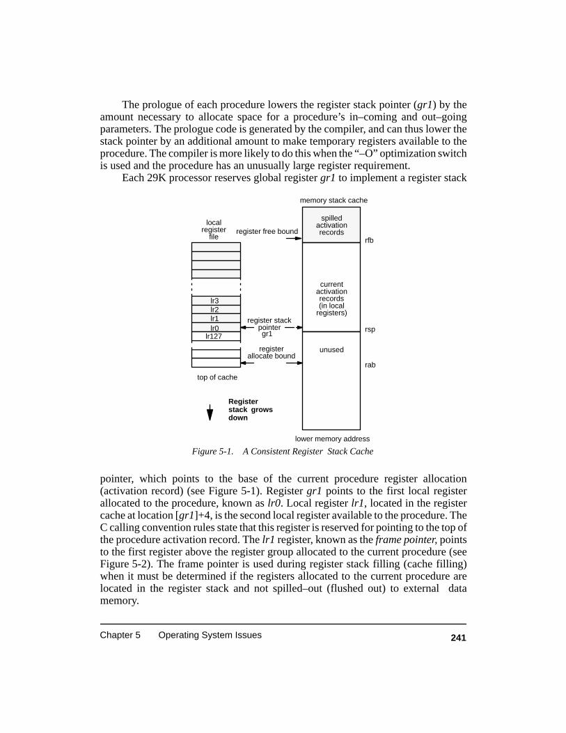
241Chapter 5 Operating System Issues
The prologue of each procedure lowers the register stack pointer (gr1) by theamount necessary to allocate space for a procedure’s in–coming and out–goingparameters. The prologue code is generated by the compiler, and can thus lower thestack pointer by an additional amount to make temporary registers available to theprocedure. The compiler is more likely to do this when the “–O” optimization switchis used and the procedure has an unusually large register requirement.
Each 29K processor reserves global register gr1 to implement a register stack
localregister
file
register stackpointer
register free boundrfb
rsp
rab
registerallocate bound
currentactivationrecords(in local
registers)
unused
lr0lr1lr2lr3
lr127
Figure 5-1. A Consistent Register Stack Cache
memory stack cache
gr1
spilledactivationrecords
Registerstack growsdown
top of cache
lower memory address
pointer, which points to the base of the current procedure register allocation(activation record) (see Figure 5-1). Register gr1 points to the first local registerallocated to the procedure, known as lr0. Local register lr1, located in the registercache at location [gr1]+4, is the second local register available to the procedure. TheC calling convention rules state that this register is reserved for pointing to the top ofthe procedure activation record. The lr1 register, known as the frame pointer, pointsto the first register above the register group allocated to the current procedure (seeFigure 5-2). The frame pointer is used during register stack filling (cache filling)when it must be determined if the registers allocated to the current procedure arelocated in the register stack and not spilled–out (flushed out) to external datamemory.
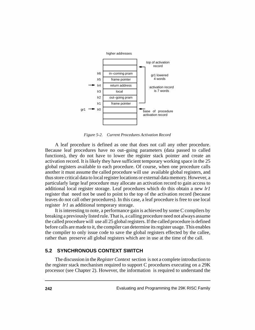
242 Evaluating and Programming the 29K RISC Family
Figure 5-2. Current Procedures Activation Record
lr0
lr1
lr2
lr3
lr4
lr5
lr6
gr1 base of procedureactivation record
top of activationrecord
higher addresses
in–coming pram
frame pointer
return address
local
out–going pram
gr1 lowered4 words
activation recordis 7 words
frame pointer
A leaf procedure is defined as one that does not call any other procedure.Because leaf procedures have no out–going parameters (data passed to calledfunctions), they do not have to lower the register stack pointer and create anactivation record. It is likely they have sufficient temporary working space in the 25global registers available to each procedure. Of course, when one procedure callsanother it must assume the called procedure will use available global registers, andthus store critical data to local register locations or external data memory. However, aparticularly large leaf procedure may allocate an activation record to gain access toadditional local register storage. Leaf procedures which do this obtain a new lr1register that need not be used to point to the top of the activation record (becauseleaves do not call other procedures). In this case, a leaf procedure is free to use localregister lr1 as additional temporary storage.
It is interesting to note, a performance gain is achieved by some C compilers bybreaking a previously listed rule. That is, a calling procedure need not always assumethe called procedure will use all 25 global registers. If the called procedure is definedbefore calls are made to it, the compiler can determine its register usage. This enablesthe compiler to only issue code to save the global registers effected by the callee,rather than preserve all global registers which are in use at the time of the call.
5.2 SYNCHRONOUS CONTEXT SWITCH
The discussion in the Register Context section is not a complete introduction tothe register stack mechanism required to support C procedures executing on a 29Kprocessor (see Chapter 2). However, the information is required to understand the

243Chapter 5 Operating System Issues
process of a synchronous context switch. In a synchronous context switch, thecurrently executing user task voluntarily gives up the processor to enable anothertask to start execution. This is normally done via a system call. Because of the Ccalling rules, the procedure which makes the system call cannot itself be a leaffunction. This means that the lr1 value of the procedure making the system callalways contains a valid pointer to the top of the current activation record. If thelibrary routine implementing the system call does not lower the register stack (inpractical terms –– it is a small leaf procedure), the current lr1 value is a valid pointerto the top of the activation record.
At first glance it seems the large number of internal registers must result in anexpensive context save and restore time penalty. Further study shows that this is notthe case.
Much of the time required to complete a context switch is associated withmoving data between external memory and internal registers. However, a significantportion of the time is associated with supervisor overhead activities.
When saving the context of the current process all the registers holding datarelevant to the current task must have their contents copied to the external datamemory save area.
A 29K processor contains a number of special purpose registers. There are eightuser task accessible special registers, sr128–sr135, used to support certaininstruction type execution. Assuming the exiting–task (the one that is being saved)was written in C and the system call library code does not contain any explicitmove–to–special–register instructions, there is no need to save the registers as anyinstructions requiring the support of special registers would have completed by thetime of the context switch system call. The AMD C calling convention does notsupport preservation of these special registers across a procedure call.
Of the 15 supervisor–mode only accessible special registers (sr0–sr14), threeregisters are allocated to controlling access to external data memory (the channelregisters). Because at the time of a synchronous context switch there is nooutstanding data memory access activity, these registers also need not be saved. Thisis only true if an instruction causing a trap is used to issue the system call and there isno outstanding data memory access DERR pending. The Am29000 processorserializes (completes) all channel activity before trap handler code commences. Formore detail on the DERR pending issue, see the Optimization section which follows.
On entering the system call procedure, the 25 global registers used by the callingprocedure no longer contain essential data. This means that they need not be saved.The register stack support registers and the relevant global supervisor registers mustbe saved.
Additionally four global registers (gr112–gr115) reserved for the user (notaffected by the compiler) must be saved if any application program uses them. Ifthese registers are not being used on a per–User basis, but shared between all Users

244 Evaluating and Programming the 29K RISC Family
and the Supervisor code, then they need not be saved. For example, a real–timesystem may chose to place peripheral status information in these registers for users toexamine. The status information may be updated by Supervisor mode interrupthandlers.
The context information is stored in a per–task data region known as the ProcessControl Block (PCB). The example task context save code below assume theregister pointing to the PCB data region, pcb, has already been assigned the correctmemory address starting value.
An operating system register in the range ks1–ks12 is assumed to point to thebottom of the PCB stack. Note that the CPS register bits set by the MTSRIMinstruction are system dependent; the RE bit may be required in some cases and theIM field value is system dependent,
.equ SIG_SYNC, –1 ;indicate a synchronous save
.equ ENABLE,(SM|PD|PI)
.equ DISABLE,(ENABLE|DI|DA)
.equ FPStat0,gr93 ;floating–point
.equ FPStat1,gr94 ;trapware support
.equ FPStat2,gr95 ;registers
sync_save : ;example synchronous context saveconstn it0,SIG_SYNCpush pcb,it0push pcb,gr1push pcb,rab ;push rabpushsr pcb,it0,pc0 ;push specialspushsr pcb,it0,pc1sub pcb,pcb,1*4 ;space pc2pushsr pcb,it0 ;push CHCpushsr pcb,it0 ;push CHDpushsr pcb,it0 ;push CHCsub pcb,pcb,1*4 ;space for alupushsr pcb,ops ;push OPSmtsrim cps,DISABLE ;remove freezesub pcb,pcb,1*4 ;space for tavmtsrim chc,0 ;possible DERR
;push pcb,lr1 ;push R–stack push pcb,rfb ; supportpush pcb,msp ;push M–stack pnt.
;mtsrim cps,ENABLE ;enable interrupts
;push pcb,FPStat0 ;floating pointpush pcb,FPStat1push pcb,FPStat2
;sub pcb,pcb,4*4 ;space for IPA..Q
;sub pcb,pcb,9*4 ;space gr116–124sub pcb,pcb,4*4 ;push gr112–115, optional

245Chapter 5 Operating System Issues
mtsrim cr, 4–1storem 0,0,gr112,pcbsub pcb,pcb,16*4 ;space for gr96–111
Local registers currently in use, those that lie in the region pointed to by gr1 andrfb (gr127), require saving. Not all of the local register cache needs saving. Theexample code below assumes the user was running with address translation on. Thus,to gain access to the user’s register stack, the Supervisor must use the UA option bitwhen storing out the cache contents. If the user had been running in physical addressmode, then there is no need for the Supervisor to use the UA option to temporarilyobtain User mode access permissions.
The context save code example above, operates with physical addresses inSupervisor mode. This means address translation is not enabled. To enable dataaddress translation when the UA bit is use, the PD bit in the CPS register must becleared. Some operating system developers may choose to run the Supervisor modecode with address translation turned on; in such cases, the PD bit will already becleared. Remember, once the PD bit is reset, it is possible to take a TLB miss. With theUA bit set during the cache store operation, the TLB miss will relate to the temporaryUser mode data memory access.
.equ UA,0x08 ;UA access
.equ PD,0x40 ;PD bit
mtsrim cps,ENABLE&~PD ;virtual data;
sub kt0,rfb,gr1 ;get bytes in cachesrl kt0,kt0,2 ;adjust to wordssub kt0,kt0,1mtsr cr,kt0storem 0,UA,lr0,gr1 ;save lr0–rfb
;mtsrim cps,ENABLE ;return to physical
5.2.1 Optimizations
When an ASSERT instruction is used to enter Supervisor mode, all outstandingdata memory access activity is completed before the trap handler gains control. If nodata access error (DERR) occurs then the channel registers will contain no valid dataand need not be saved. However, when the channel access is serialized and forced tocomplete, a priority four DERR may have occurred. The DERR trap competes withthe priority three system call trap (higher than four), and thus the system call traphandler commences but with the channel still containing information pertaining tothe failed data access.
A performance gain can be obtained by not saving the channel registers toexternal data memory. If the memory system hardware is unable to generate theDERR signal, then the channel registers should not be saved. Additionally, if the

246 Evaluating and Programming the 29K RISC Family
software developer knows the previous data memory access has been completed orwas to a known memory location, there may be no need to save the channel registers.The code shown below is an alternative to the previous system call trap handler entrycode, the transaction–fault bit (TF) in the channel control register (CHC) is tested todetermine if channel registers need saving.
A further performance gain can be obtained by not saving the PC0 register.When the PC1 register is restored, the PC0 register can be determined by adding 4 tothe PC1 address value. To achieve the best performance gains, the code in thesubsequent Restoring Context section may be optimized to avoid restoring channelregisters CHA and CHD if the CHC contents–valid (CV) bit is zero.
save_channel: ;deal withpushsr pcb,it0,cha ;DERR faultpushsr pcb,it0,chdpushsr pcb,it0,chcjmp channel_saved mtsrim chc,0 ;clear TF
sync_save : ;example synchronous context saveconstn it0,SIG_SYNCpush pcb,it0push pcb,gr1push pcb,rab ;push rabsub pcb,pcb,1*4 ;space for pc0pushsr pcb,it0,pc1 ;push pc1sub pcb,pcb,1*4 ;space for pc2mfsr it0,chc ;test TF bitsll it0,it0,31–10 ; in CHC setjmpt it0,save_channel sub pcb,pcb,2*4 ;space for cha,chdconst it0,0push pcb,it0 ;push CHC=0
channel_saved:sub pcb,pcb,1*4 ;space for alupushsr pcb,ops ;push OPSmtsrim cps,DISABLE ;remove freezesub pcb,pcb,1*4 ;space for tav
When restoring the task currently being saved, it is not necessary to reload all128 local registers, or even the part of the register file in use at context save time([gr1]––[rfb]). Only the activation record of the last executing procedure for the task([gr1]––[lr1]) (see Figure 5-3). This greatly reduces the time required to restore atask context originally saved by a synchronous context switch. Typically the size of aprocedure activation record ([gr1]–––[lr1]) is twelve words. To achieve thisoptimization, the push of rab and rfb, shown in the previous code fragment, must bechanged to the code shown below. This ensures only one activation record is restored.

247Chapter 5 Operating System Issues
Figure 5-3. Overlapping Activation Records Eventual Spill Out of the Register Stack Cache
frame pointer
top of activationrecord
lr0
lr1
lr2
lr3
lr4
lr5
lr6
top of activationrecord
higher addresses
in–coming pram
frame pointer
return address
local
out–going pram
frame pointer
frame pointer
Cache resident
Memory resident
rfb
top of stackgr1
Activation recordof last executingprocedure
Activation recordonly partially in cache
.equ WS,512 ;Window Size
const it0,WS ;replacement forsub rab,lr1,it0 ; push rabpush pcb,rab ;push lr1–512
;push pcb,lr1 ;replacement for push rfb

248 Evaluating and Programming the 29K RISC Family
Burst mode enables data to be loaded–from or stored–to memory consecutively,without the processor continuously supplying addresses information. An externaladdress latch/counter is required to support such memory systems with an Am29000
signal number
PC0
PC1
PC2
CHA
CHD
CHC
ALU
OPS
tav
Figure 5-4. Context Save PCB Layout
the stack is shown withhigher addresses at thetop of the figure, and loweraddresses at the bottom.
gr1
rab
lr1
rfb
gr112–gr115
floating point support
gr96–gr111
gr116–gr124
signal number
PC0
PC1
PC2
CHA
CHD
CHC=0
ALU
OPS
tav
gr1
rab
Interrupt Frame System Call Frame
Async. Save Frame Sync. Save Frame
stackgrowsdown
enable interrupts
IPB
IPC
Q
lr1
rfb
gr112–gr115
floating point support
gr96–gr111
gr116–gr124
rfbIPA
IPB
IPC
Q
IPA
mspmsp
registers not normaly saved

249Chapter 5 Operating System Issues
or Am29050 processor. A system designer can use this feature to reduced contextswitch times.
5.3 ASYNCHRONOUS CONTEXT SWITCH
An asynchronous context switch occurs when the current task unexpectedlygives up the processor to enable another task to execute. This may occur when a timerinterrupt results in the supervisor deciding the current task is no longer the task ofhighest priority. Unlike at the point at which a synchronous context switch occurs,when an interrupt occurs the state of the processor is not restricted to a simple state.
Because an interrupt may occur in a leaf procedure, it is not possible todetermine if the current lr1 value contains a valid pointer to the top of the procedureactivation record. Further, the interrupt may have occurred during a procedureprologue, where the register stack pointer (gr1) has been lowered but the lr1 valuehas not yet been updated. This means when an asynchronous–saved task is switchedback in, it is impossible to restore only the activation record of the interruptedprocedure. The register stack containing valid data, that is [gr1]––[rfb], must berestored. Assuming this amounts to half of the register file, an additional 2.6 microseconds would be required to restore the task with a single–cycle Am29000processor memory system at 25MHz.
A task voluntarily giving up the processor via a system call from within aprocedure of typical activation record size can be restored faster then a task giving upthe processor involuntarily via an asynchronous interrupt.
When a User mode program is interrupted it could mean the current process is tobe sent a signal, such as a segmentation violation. It could also mean that theSupervisor wishes to gain control of the processor to support servicing theinterrupting device. If the current process is being signaled, the label user_signalshould be jumped to by Supervisor mode interrupt handler (see the example codebelow). This is explained in the later section titled User Mode Signals (section 5.5). IfSupervisor support code is required for peripheral device servicing, then the action tobe taken is very much dependent on the interrupting device needs.
.equ SIGALRM,14 ;alarm signal
time_out: ;timer interrupt handlerjmp interrupt_common const it0,SIGALRM ;signal number
interrupt_common:
;Depending on required processing,;jump to user_signal for current process signaling.;Or, jump to user_interrupt to save the current process context.
Some interrupts can be serviced in Freeze mode, without the need to save thecurrent process context. Use of these so–called lightweight interrupt handlers can
250 Evaluating and Programming the 29K RISC Family
offer significant performance gains. Other interrupts will require the interruptedprocess context to be saved. This is described in the following section, InterruptingUser Mode (section 5.4).
It is possible an interrupt has arrived that requires a signal to be sent to a processwhich is not the currently executing process. In this case, the operating system mustfirst save the current process context and then restore the context of the signaledprocess. Once the in–coming process is prepared to run, using the code in the RestoreContext section (section 5.10), the restored context will have to be then placed on thesignal stack as described in the User Mode Signals (section 5.5). Thus, executionwould begin in the User mode trampoline code of the in–coming process. To followthis in detail, later sections of the chapter shall have to be studied.
5.4 INTERRUPTING USER MODE
This section describes how the operating system can prepare the processor toexecute a C level interrupt handler, where the handler is to run in Supervisor modeand the interrupt occurred during User mode code execution.
Because the User mode task is being asynchronously interrupted, the completeprocessor state must be saved. The context information should be stored in the PCBrather than a temporary stack, as a context switch to a new user task may occur afterthe interrupt has been processed. Storing the state in the PCB saves having to copythe state from the temporary stack to the PCB after the context switch decision hasbeen made. When saving task context, a performance optimization is obtained byonly saving the registers which are currently in use. However, such optimizationstypically only apply to synchronous–task context saving.
When User mode is interrupted, the special purpose support registers maycontain valid data. This means an additional nine special register data values must becopied to external data memory, compared to the synchronous context switch.
Below is a code example of interrupt context saving. Notice the rab stacksupport register is adjusted to a window distance below rfb within the interruptdisabled portion of the code. This is to conform to the same PCB format used by thosewho wish to perform the register stack fix–up with User mode code, rather than in theSupervisor code shown. Register rab is merely a convenience value for determiningrfb–WindowSize (WindowSize normally 512) in detecting a SPILL condition.However, it is also used to determine FILL or SPILL interruption. Should the Usermode stack fix–up code be interrupted during it’s operation, it is important that it doesnot become confused with the original SPILL or FILL interrupt. Realigning the rabregister whilst interrupts are off prevents this confusion.
.equ WS,512 ;Window Size
user_interrupt : ;saving User mode contextpush pcb,it0 ;stack signal id

251Chapter 5 Operating System Issues
push pcb,gr1push pcb,rab ;stack real rabconst it0,WSsub rab,rfb,it0 ;set rab=rfb–512
;pushsr pcb,it0,pc0 ;push specialspushsr pcb,it0,pc1pushsr pcb,it0,pc2pushsr pcb,it0,chapushsr pcb,it0,chdpushsr pcb,it0,chcpushsr pcb,it0,alupushsr pcb,it0,opsmtsrim cps,DISABLE ;remove freezepush pcb,tavmtsrim chc,0 ;clear CHC
;push pcb,lr1 ;push R–stack push pcb,rfb ; supportpush pcb,msp ;M–stack pnt.
;mtsrim cps,ENABLE ;enable interrupts
;push pcb,FPStat0 ;floating pointpush pcb,FPStat1push pcb,FPStat2
;pushsr pcb,kt0,ipa ;more specialspushsr pcb,kt0,ipbpushsr pcb,kt0,ipcpushsr pcb,kt0,q
The 25 global registers, known to contain no valid data during a synchronouscontext switch, must also be considered active, and consequently saved. Becausethese global registers are located adjacent to the four global registers reserved for theuser, a single store–multiple instruction can be used to save the relevant globalregisters. Considering a single–cycle memory system, two micro seconds should berequired to save the additional current task context.
sub pcb,pcb,29*4 ;push gr96–gr124mtsrim cr,29–1 ;including optional save of storem 0,0,gr96,pcb ; gr112–gr115
If the interrupt is expected to result in a context switch then the local registerscurrently in use require saving. Note, this can be postponed (see the followingoptimizations section). Not all of the local register cache needs to be saved. However,as is explained below, do not simply assume that those that lie in the region pointed toby gr1 and rfb (gr127) are the only active cache registers.
When a synchronous context switch occurs the register stack is known to be in avalid condition (see Figure 5-1). With an asynchronous event causing a context

252 Evaluating and Programming the 29K RISC Family
switch, the stack may not be in a valid condition. There are three inconsistentsituations that must be detected and dealt with.
The interrupt occurred when a SPILL was in progress, in which case thedistance between the values in the rfb and rab registers exceeds the size of thelocal register file (referred to as the Window Size). All of the local register filemust be saved. Some of the cached data may have already been copied out tomemory locations just below rfb. This data should remain at this location on thememory resident portion of the stack until the task is restarted.
The interrupt occurred when a FILL operation was in progress, in which casethe distance between the values in the rfb and rab registers is less than the size ofthe local register file. Some data may have been copied in from the top of thememory resident portion of the register stack into local registers just above rab.These registers will not be saved during the normal cache save ([gr1]–[rfb] ). Todeal with this the FILL must be restarted when the context is restored.
The interrupt occurred during a far–longjmp operation. A far–longjmp isdefined as one in which the future (gr1 + 8) value—which is the address of localregister lr2 on the register memory stack—is greater than the current value inthe rfb register. In this case the local registers contain no valuable data because aprevious activation record (present during setjmp) is about to be restored fromthe memory resident portion of the stack.
.equ WS,512 ;Window Size
R_fixup: ;register stack fix–upadd kt0,pcb,CTX_RABload 0,0,kt2,kt0 ;get rab valuesub kt0,rfb,kt2 ;window sizesrl kt0,kt0,2 ;convert to wordscpeq kt1,kt0,WS>>2 ;test for validjmpt kt1,norm ; stack condition cpltu kt1,kt0,WS>>2 ;test for FILLjmpt kt1,ifill ; interrupt add kt1,gr1,8 ;test far–longjmpcpgtu kt1,kt1,rfb ; interruptjmpt kt1,illjmp ;yes, gr1+8 > rfb nop
;ispill: ;deal with interrupted SPILL
const kt1,WSjmp norm ;gr1=rfb–512 sub gr1,rfb–kt1
;ifill: ;deal wilth interrupted FILL
add kt1,pcb,CTX_CHCconst kt0,0push kt1,kt0 ;resave CHC=0

253Chapter 5 Operating System Issues
add kt0,FillAddrReg,4add kt1,pcb,CTX_PC0push kt1,kt0 ;resave PC0,PC1push kt1,FillAddrRegadd kt1,pcb,CTX_RABpush kt1,rab ;resave rab=rfb–512
;norm: ;deal with consistant stack
sub kt1,rfb,gr1 ;bytes in cachesrl kt1,kt1,2 ;convert to wordssub kt1,kt1,1 ;adjust for storemmtsrim cr,kt1mtsrim cps,ENABLE&~PD ;virtual datastorem 0,UA,lr0,gr1 ;copy to stackmtsrim cps,ENABLE ;physical data
;illjmp: ;valid local registers now saved
Once the user’s User mode register stack has been saved, the interrupt handlercontinues using the user’s Supervisor mode register and memory stacks.
.macro const32,reg,dataconst reg,data ;zero high, set lowconsth reg,data ;high 16–bits.endm
const32 msp,SM_STACK ;Supervisor M–stackconst32 rab,SR_STACK–WSadd gr1,rfb,8 ;prepare Supervisorconst32 rfb,SR_STACK ; R–stack supportadd lr1,rfb,0 ; registers
;;call appropriate C–level interrupt handler
The current task context has now been saved. After the interrupt has beenprocessed the operating system can select a different task to restore. This operation isdescribed in a subsequent section entitled Restoring Context (section 5.10). The PCBstructure for the out–going task shall not be accessed until the task is again restored asthe current executing task.
5.4.1 Optimizations
When User mode is interrupted, processing continues using the user’sSupervisor mode stacks. This is necessary because the interrupt may result in theprocess being put to sleep until some time later when it is again able to run. When theprocess is put to sleep, the process state is stored in the Supervisor memory stack,described in the Interrupting Supervisor Mode section (section 5.6). If the user’sUser mode context was saved on a shared interrupt stack rather than the per–processSupervisor stack, then the context would have to be copied from the global interruptstack to the Supervisor stack before a context switch could proceed.

254 Evaluating and Programming the 29K RISC Family
The code shown above determines the region of cache registers currently in useand stores them out onto the top of the user’s User mode register stack. This operationcan be postponed. The interrupt handler will use the register cache in conjunctionwith the Supervisor mode register stack. If the interrupt handler runs to completionand no context switch occurs, then the cache need not be saved. If a context switchdoes occur then the cache will be saved on the top of the user’s Supervisor moderegister stack. This means some User mode data contained in the cache may betemporary saved on the the Supervisor stack; however, this is not a problem.
The previous code determines the region of the cache currently in use, it doesnot bring the stack into a valid condition. The code following the label R_fixup: inthe User Mode Signals section (section 5.5) does bring the stack into a validcondition, and can be used to replace the code shown above. Once the stack supportregisters are restored to a valid state, the stack–cut–across method described in thelater User System Calls section (section 5.7) can be used to attach the cache to theSupervisor mode stack. By this method the storing of cache data can be prevented andany unused portion of the cache is made immediately available to the interruptservice routine.
5.5 PROCESSING SIGNALS IN USER MODE
Asynchronous context switches often occur because an interrupt has occurredand must be processed by a handler function developed in C. A technique oftenoverlooked in real–time applications is using a signal handler to process the interrupt.This often avoids much of the supervisor overheads associated with a context switch.Additionally, a context switch requires the instruction cache to be flushed. Signalhandlers run in the context of the interrupted User mode process, this avoids the needto flush the cache.
It is not necessary to store the contents of the local register file. After signalsupport code has fixed–up the stack management support registers, the C levelhandler code can continue to use the register stack as if the interrupted procedure hadexecuted a call to the handler function. In as little as 5.5 micro seconds from the timeof receiving the interrupt, the Am29000 can be executing the interrupt handler codewhich was written in C.
Unlike asynchronous context switching, the interrupted context can not besaved in the PCB. To do so would be convenient if a context switch was possible afterthe signal handler had finished executing. The PCB structure would be alreadyupdated. However, a further interrupt may occur during the C level signal handlerexecution, which may itself result in an immediate context switch and require the useof the PCB data save area. Additionally, the signal handler may do a longjmp to asetjmp which occurred in User mode code before the signal handler startedexecuting. For this reason the context information is placed on the User’s memorystack pointed to by msp.

255Chapter 5 Operating System Issues
Users of operating systems complying with the AMD HIF–specification arerequired to complete signal handler preparation tasks in User mode code supplied inAMD libraries. HIF compliant operating systems only save the signal–numberthrough the tav register portion of the interrupt frame on the user’s memory stack.The remaining part of the interrupt frame is saved by the user’s code. Any necessaryregister stack management is performed. The User mode code is shown in AppendixB and described in detail in section 4.4. The following code is for operating systemswhich save the complete interrupt frame and prepare for a User mode signal while inSupervisor mode
.equ SIGILL,4 ;illegal operation
.equ WS,512 ;Window Size
protect: ;Protection violation trap handlerjmp user_signal ;send interrupted task a signal const it0,SIGILL ;signal number
If the interrupted User mode code was running with address translation turnedon, then the user’s memory stack must be accessed by the Supervisor using the UA bitduring LOAD and STORE instructions (note, this is also true for the push and pushsrmacros). The following code example shows pushing onto a physically accessibleuser memory stack. If the user’s stack were virtually addressed, then the pushinstructions would be replaced by move to temporary register instructions. Afterinterrupts were enabled the PD bit in the CPS register would be cleared to enable dataaddress translation, and then the temporary registers would be pushed onto the user’smemory stack using the UA bit during the STORE instruction operation. Once thefrozen special registers had been saved, via the use of temporary registers, theSupervisor could continue to run with the CPS register bits PD and DA cleared, andstore the remaining user state via push operations.
user_signal : ;prepare to process a signalpush msp,it0 ;stack signal idpush msp,gr1const it0,WSsub rab,rfb,it0 ;set rab=rfb–512
;pushsr msp,it0,pc0 ;push specialspushsr msp,it0,pc1pushsr msp,it0,pc2pushsr msp,it0,chapushsr msp,it0,chdpushsr msp,it0,chcpushsr msp,it0,alupushsr msp,it0,opsmtsrim cps,DISABLE ;remove freezepush msp,tavmtsrim chc,0 ;clear CHC
;
256 Evaluating and Programming the 29K RISC Family
push msp,lr1 ;push R–stack push msp,rfb ; supportpush msp,msp ;M–stack support
;mtsrim cps,ENABLE ;enable interrupts
;push msp,FPStat0 ;floating pointpush msp,FPStat1push msp,FPStat2
;pushsr msp,kt0,ipa ;more specialspushsr msp,kt0,ipbpushsr msp,kt0,ipcpushsr msp,kt0,q
;sub msp,msp,29*4 ;push gr96–gr124mtsrim cr,29–1 ;including optional save of storem 0,0,gr96,msp ; gr112–gr115
The register stack must now be brought into a valid condition, if is not already ina valid condition. Valid is defined as consistent with the conditions supporting afunction call prologue. As described in the previous section 5.3, AsynchronousContext Switching, the stack may not be valid if a SPILL , FILL or far–longjmp isinterrupted.
Unlike the asynchronous context save case, with signal processing our intentionis not to simply determine the active local registers for saving on the user’s memoryportion of the register stack, but to enable the user to continue making function callswith the existing stack. That is, the C language signal handler will appear to havebeen called in the normal manner, rather than as a result of an interrupt.
; Register stack fixupR_fixup:
const kt0,WS ;WindowSizeadd kt2,msp,CTX_RABload 0,0,kt2,kt2 ;interrupted rabsub kt1,rfb,kt2 ;determine ifcpgeu kt1,kt1,kt0 ;rfb–rab>=WindowSizejmpt kt1,nfill ;jmp if spill
;or valid stack add kt1,gr1,8 ;check if cpgtu kt1,kt1,rfb ; gr1+8 > rfbjmpt kt1,nfill ;yes, long–longjmp nop
;ifill: ;here for interrupted FILL restart
add kt1,msp,CTX_CHCconst kt0,0push kt1,kt0 ;resave CHC=0add kt0,FillAddrReg,4add kt1,msp,CTX_PC0push kt1,kt0 ;resave PC0,PC1push kt1,FillAddrReg

257Chapter 5 Operating System Issues
add kt1,msp,CTX_RABpush kt1,rab ;resave rab=rfb–512
;nfill: ;move gr1 into valid range
cpgtu kt0, gr1, rfb ;if gr1 > rfbjmpt kt0, lower ;far–longjmp casecpltu kt0, gr1, rab ;if gr1 < rab then jmpf kt0, sendsig ;interrupted spill nop
raise:add gr1, rab, 0jmp sendsig nop
lower:add gr1, rfb, 0jmp sendsig nop
Now use the signal number to determine the address of the corresponding signalhandler. The code below assumes there is an array of signal handlers. The first entryof the array is held at memory address SigArray.
sendsig: ;prepare to leave Supervisor modeadd kt0,msp,CTX_SIGNUMBload 0,0,gr96,kt0 ;get signal numb.sub kt2,gr96,1 ;handler index...sll kt2,kt2,2 ; ...in wordsconst kt1,SigArrayconsth kt1,SigArrayadd kt2,kt2,kt1load 0,0,gr97,kt2 ;handler adds.
;mtsrim cps,FREEZE ;enter Freeze modeconst kt1,_trampolineadd kt0,kt1,4mtsr pc1,kt1 ;return to usermtsr pc0,kt0 ;and process signaliret
Via an IRET, execution is continued in User mode procedure trampoline. Thisprocedure is often located in the memory page containing the PCB structure. UsingUser accessible global registers gr96 and gr97, two parameters, the signal numberand a pointer to the signal handler routine, are passed to the trampoline code. Thehandler routine is called, passing to it the signal number and a pointer to the savedcontext.
;User mode entry to signal handler_trampoline: ;Dummy Call
sub gr1,gr1,6*4 ;space for C–callasgeu V_SPILL,gr1,rabadd lr1,gr1,6*4add lr0,gr97,0 ;copy handler()

258 Evaluating and Programming the 29K RISC Family
add lr2,gr96,0 ;copy signal #add lr3,msp,0 ;pass CTX pointer
;calli lr0,lr0 ;call handler() nop
;add gr1,gr1,6*4 ;restore stack nopasleu V_FILL,lr1,rfbconst tav,SYS_SIGRETURNasneq V_SYSCALL,gr1,gr1 ;system call
After the signal handler returns, the interrupted context is restored via thesigreturn system call. The supervisor mode code used to implement the restorationprocess is shown in the section titled Restoring Context (section 5.10). At the time ofthe system call trap, the memory stack pointer, msp, must be pointing to the structurecontaining the saved context. The system call code checks relevant register data toensure that the User is not trying to gain Supervisor access permissions as a result ofmanipulating the context information during the signal handler execution. (Note, it islikely that assembly code library supporting the sigreturn system call shall copy thelr2 parameter value to the msp register before issuing the system call trap.)
5.6 INTERRUPTING SUPERVISOR MODE
A user program may be in the process of executing a system call when aninterrupt occurs. This interrupt may require C level handler processing. In somerespects this is similar to a user program dealing with a C level signal handler;however, there are some important differences. A User mode signal handlers maychose not to run to completion by doing a longjmp out of the signal handler. Also,signal handlers process User mode data. Supervisor mode interrupt handlers alwaysrun to completion and process data relevant to the Supervisor’s support task ratherthan the current User mode task.
Because a user task is being interrupted whilst operating in Supervisor mode,the complete processor state must be saved in a similar way to an asynchronouscontext switch. The context information can not be stored in the current user’s PCBbecause it is used to hold the User mode status when Supervisor mode is entered via asystem call.
User programs usually switch stacks when executing system calls (see section5.7). The user’s system stack is not accessible to the User mode program. This keepsSupervisor information that appears on the stack during system call execution hiddenfrom the user. The user’s system stack can be used to support C function calls duringinterrupt handler processing. Alternatively, an interrupt processing stack can beused. Keeping a separate interrupt stack for Supervisor mode interrupt processingenables a smaller system mode User stack to be supported, as the interrupt processing

259Chapter 5 Operating System Issues
does not cause the system stack to grow further. Remember, the per–user systemstack is already in use because the user was processing a system call when theinterrupt occurred.
The interrupt_common entry point to the interrupt handler shown inAsynchronous Context Switch (section 5.3) needs to be expanded to distinguishbetween interrupting User mode and interrupting Supervisor mode. The appropriateprocessing requirement is determined by examining the OPS register in the interrupthandler. The label user_interrupt should be used to select the code for an interrupt ofUser mode code.
interrupt_common: ;examine processor mode interruptedmfsr it1,ops ;get OPS specialsll it1,it1,27 ;check SM bitjmpf user_interrupt ;User mode inter. nop
The following code assumes Supervisor mode interrupts are not nested, becausethe current context is pushed onto the interrupt processing stack which is assumedempty. If interrupts are to be nested, then the context should be pushed on the currentmemory stack once it has been determined that the msp has already been assigned tothe interrupt memory stack. IM_STACK and IR_STACK are the addresses of thebottom of the interrupt memory and register stacks respectively.
.equ WS,512 ;Window Size
.macro const32,reg,dataconst reg,data ;zero high, set lowconsth reg,data ;high 16–bits.endm
supervisor_interrupt : ;process Supervisor mode interruptconst32 it1,IM_STACK ;interrupt M–stackpush it1,it0 ;stack signal idpush it1,gr1const it0,WSsub rab,rfb,it0 ;set rab=rfb–512
;pushsr it1,it0,pc0 ;push specialspushsr it1,it0,pc1pushsr it1,it0,pc2pushsr it1,it0,chapushsr it1,it0,chdpushsr it1,it0,chcpushsr it1,it0,alupushsr it1,it0,opsmtsrim cps,DISABLE ;remove freezepush it1,tav
;mtsrim chc,0 ;clear CHC
;
260 Evaluating and Programming the 29K RISC Family
push it1,lr1 ;push R–stackpush it1,rfb ; supportpush pcb,msp ;push M–stack pntr.add msp,it1,0 ;use msp pointer
;mtsrim cps,ENABLE ;enable interrupts
;push msp,FPStat0 ;floating pointpush msp,FPStat1push msp,FPStat2
;pushsr msp,kt0,ipa ;more specialspushsr msp,kt0,ipbpushsr msp,kt0,ipcpushsr msp,kt0,q
;sub msp,msp,29*4 ;push gr96–gr124mtsrim cr,29–1 ;including optional save of storem 0,0,gr96,msp ; gr112–gr115
There is no need to save any of the register cache data. In the following code, theregister stack support registers are updated with the initial values of the supervisorinterrupt stack. If nested high level handler interrupts are to be supported, see thefollowing Optimizations section. The gr1 register stack pointer is then set to the top(rab) of the cache, indicating the cache is fully in use. The new activation record sizepointer, lr1, is then set to the bottom of the cache (rfb).This ensures that when theinterrupted C level service function returns, the cache will be repaired to exactly theposition at which the interrupt occurred. This is particularly important if a Supervisormode FILL was interrupted. The user’s system mode register data will be spilledonto the interrupt stack, but this creates no problem.
const32 rab,IR_STACK–WSadd gr1,rab,0 ;prepare interruptconst32 rfb,IR_STACK ; R–stack supportadd lr1,rfb ; registers
;;call appropriate C–level interrupt handler
5.6.1 Optimizations
The code shown above does not attempt to determine the region of cacheregisters currently in use. This means that the first C level procedure call in theinterrupt handler will result if a cache spill trap occurs.
By determining the region of the cache currently in use and by bringing theregister stack into a valid condition, any available cache registers can be madeimmediately available to the interrupt handler C routines. The code following thelabel R_fixup: in the previous User Mode Signals section (section5.5) does bring the

261Chapter 5 Operating System Issues
stack into a valid condition and can be used to replace the code shown above. Oncethe stack support registers are restored to a valid state, the stack–cut–across methoddescribed in the User System Calls section (section 5.7) can attach the cache to theinterrupt register stack.
It is possible that while processing an interrupt (which means the processor isalready in Supervisor mode) an additional interrupt occurs. If an operating systemsupports nested interrupts, then the code in the Interrupting Supervisor Mode section(section 5.6) will be executed again. This overhead can be avoided by following theInterrupt Queuing Model method described in section 4.3.12 of the Interrupts andTraps chapter.
The method relies on supporting only lightweight interrupt nesting. The code inthis section is entered only once to start the execution of a C level interrupt processingDispatcher. Each interrupt adds a interrupt request descriptor (bead) on to a queue ofdescriptors (string of beads). The dispatcher removes the requests and processes theinterrupt until the list becomes empty. Lightweight interrupts enable the externaldevice to be quickly responded to, although the dispatcher may not complete theprocessing till some time later.
5.7 USER SYSTEM CALLS
User programs usually switch stacks when executing system calls. The user’ssystem stack is not accessible to the User mode program. This keeps Supervisorinformation which appears on the stack during system call execution hidden from theuser.
Synchronous context switching generally happens as a result of a system call.However, system calls are also used to request the operating system to obtaininformation for a user which is only directly obtainable with Supervisor accessprivileges. The user’s state must be saved to the PCB structure in a similar way to asynchronous context save. This makes the global and special registers available forSupervisor mode C function use. There is no need to save the register cache until afull context switch is known to be required.
.equ SIG_SYNC, –1
.equ ENABLE,(SM|PD|PI)
.equ DISABLE,(ENABLE|DI|DA)
syscall: ;V_SYSCALL trap handlerconstn it0,SIG_SYNC ; assumes nopush pcb,it0 ; outstanding DERRpush pcb,gr1 ;push gr1push pcb,rab ;push rabpushsr pcb,it0,pc0 ;push specialspushsr pcb,it0,pc1sub pcb,pcb,3*4 ;space pc2,cha,chdconst it0,0

262 Evaluating and Programming the 29K RISC Family
push pcb,it0 ;push CHC=0sub pcb,pcb,1*4 ;space for alupushsr pcb,ops ;push OPSmtsrim cps,DISABLE ;remove freezesub pcb,pcb,1*4 ;space for tav
;push pcb,lr1 ;stack supportpush pcb,rfb ;push rfbpush pcb,msp ;push M–stack pnt.
;mtsrim cps,ENABLE ;enable interrupts
;push pcb,FPStat0 ;floating pointpush pcb,FPStat1push pcb,FPStat2
;;Assume the same gr112–gr115 data is shared;by all users and the supervisor, and ;therefor will not push gr112–gr115.;;Align pcb for system call return
sub pcb,pcb,(4+(124–96+1))*4
The system call code can continue to use the cache attached to the user’s systemmode registers stack. To do this the current top of stack position, gr1, must bemaintained. The register stack support registers are relocated to the system stack,maintaining the existing stack position offset. The following code performs this stackcut–across operation. It assumes the system call is made from a valid stack condition.However, it includes bounds protection because operating systems can nevercompletely rely on users always maintaining valid stack support registers.
sub gr96,rfb,gr1 ;determine rfb–gr1andn gr96,gr96,3 ;stack is double word alignedconst gr97,(128*4) ;max allowed value for cpleu gr97,gr96,gr97 ; rfb–gr1 is 128*4jmpt gr97,$1 ;jump if normal register usage const gr97,0x1fc ;mask for page displacement mathconst gr96,512 ;limit register use to max (512)
$1: and gr1,gr1,gr97 ;determine gr1 displacement withinconst gr97,SR_STACK–1024; 512–byte pageconsth gr97,SR_STACK–1024;add gr1,gr1,gr97 ;gr1=SR_STACK–1024+displacementadd rfb,gr1,gr96 ;rfb=(new gr1)+const gr97,(128*4) ; min(512,rfb–gr1))sub rab,rfb,gr97 ;set rab=rfb–512add lr1,rfb,0 ;ensure all User mode registers
; restored
The technique relies on keeping bits 8–2 of the stack pointer, gr1, unchanged. Inother words, the lr0 register has the same position in the cache after the memoryresident stack portion has been exchanged. This is achieved by calculating the

263Chapter 5 Operating System Issues
address displacement of gr1 within a 512–byte page size. The gr1 displacementremains the same if the memory resident portion of the register stack has beenexchanged. SM_STACK and SR_STACK are the addresses of the bottom of theper–user system memory and register stacks respectively (see Figure 5-5).
Figure 5-5. Register Stack Cut–Across
SR_STACK
UR_STACK
gr1
rfb
Supervisor ModeRegister stack
User ModeRegister stack
SR_STACK
UR_STACK
gr1
rfb
512–bytepage bound-aries
Register stacksupport registersbefore systemcall
Register stack supportregisters after stackcut–across
pagedisplacement
registersormemory inuse
registercacheportion ofregisterstack
Once stack cut–across has been completed, a call to the C level system callhandler can be issued. The C code may get its incoming parameters from the registerstack, or the system call trap handler code may copy the parameters from the localregisters to memory locations accessible by the Supervisor mode C handler.
;copy lr2,... arguments to memory locationsadd gr96,tav,0 ;save service numb.sub gr1,gr1,4*4 ;new stack frameasgeu V_SPILL,gr1,rabadd lr1,gr1,4*2 ;ensure lr1 restoreconst32 lr0,_syscall ;C handlercalli lr0,lr0 ; call add lr2,gr96,0 ;pass service numb.
The C system call handler may place its return values in known memorylocations, rather than global registers gr96–gr111. If this is the case, then the valuesshall have to be copied to the normal return registers. System calls indicate theirsuccessful or unsuccessful completion to their callers by setting register tav (gr121)

264 Evaluating and Programming the 29K RISC Family
to TRUE or FALSE; the high level handler achieves this by modifying the gr121register location in the PCB before the system call return code is executed. A FILLassertion is used to repair the cache to the position at which the system call wasissued.
add gr1,gr1,16 ;restore systemnop ; call frame lr1asleu V_FILL,lr1,rfb ;restore all cache
;copy return values from memory to gr96,...jmp resume ;restore context nop
Because a User mode signal handler may use the system call mechanism to issuea sigreturn, it is possible an asynchronous context restore may be required in place ofthe normal synchronous context restore associated with a system call. Label resumeis jumped to and is described in the Restore Context section (section 5.10). If anasynchronous context is being restored, then a pointer to the context being restoredwill have been passed to the sigreturn system call. The high level C handler will havecopied this data over the PCB data stored at the time of the system call trap entry. TheC handler must change the SIG_SYNC value stored in the PCB by the system calltrap handler. This will cause the resume code to perform an asynchronous rather thansynchronous context restore.
5.8 FLOATING–POINT ISSUES
The example code presented saves only three supervisor accessible globalregisters under the heading floating–point support. These registers are typicallyks13–ks15. This is sufficient to save and restore floating–point context when anAm29000 processor is being used with trapware emulation. This is only true ifinterrupts are turned off during floating–point trapware execution. If floating–pointtrapware is interruptible, then the Am29000 trapware support registers (typicallyit0–it3 and kt0–kt11) would have to be saved.
When an Am29027 floating–point coprocessor is used, either inline or viatrapware support, the complete state of the coprocessor must be saved. This requiresan additional 35 words space in addition to the three Am29000 global supportregisters.
Some real–time operating systems may run floating–point trapware withinterrupts off and chose to save no floating support registers at all. This will improvecontext switch times. User programs typically only change the rounding modeinformation in the support registers. If all user tasks run with the same roundinginformation, then there is no need to save and restore the three floating–point supportregisters.
The Am29050 directly executes floating point instructions without the need fortrapware. It has four floating point support registers, special registers sr160–162 and

265Chapter 5 Operating System Issues
sr164. In fact, the three support registers required by the Am29000 are used tovirtualize these Am29050 registers. Saving Am29050 floating point context wouldbe achieved by saving these four registers and the four double word accumulatorvalues. However, the Am29050 does not directly support integer DIVIDE andDIVIDU instructions. The trapware which implements these instructions requiressix support registers (typically kt0–kt5). If this trapware is interruptable, then theseregisters would also have to be saved.
5.9 DEBUGGER ISSUES
Debuggers such as AMD’s MiniMON29K monitor have a special contextswitch requirement. They need to be able to switch context to the debugger from arunning application or operating system without losing the contents of any processorregister. One possibility is to reserve a global register in the range gr64–gr95,specifically for debugger support. But, most operating system developers areunwilling to give up a register.
A technique which avoids losing a register for operating system use is to use gr4to first store a single operating system register, and then use this register to startsaving the rest of the processor context. The Am29000 does not have a gr4 registerbut the ALU forwarding logic enables this technique to work. The code examplebelow, taken from MiniMON29K, shows how the processor context save getsstarted. Note, _dbg_glob_reg is the memory address used by the debugger to saveglobal registers.
.macro const32,reg,dataconst reg,data ;zero high, set lowconsth reg,data ;high 16–bits.endm
dbg_V_bkpt:const32 gr4,_dbg_glob_reg+96*4store 0,0,gr96,gr4 ;save gr96const32 gr96,_dbg_glob_reg+97*4store 0,0,gr97,gr96 ;save gr97add gr96,gr96,4store 0,0,gr98,gr96 ;save gr98
;call gr96,store_state const gr97,V_BKPT
Label dbg_V_bkpt is the address vectored to by an illegal opcode(MiniMON29K uses these to implement breakpoints on the Am29000). Whenfunction store_state is reached, global registers gr96–gr98 have already been saved.
The gr4 user should be careful to remember that the Am29000 ALU forwardinglogic only keeps the gr4 register value alive for 1–cycle following its modification.Additionally, because emulators also make use of gr4 in analyzing processor
266 Evaluating and Programming the 29K RISC Family
registers, it is not possible to use an emulator to debug the monitor entry code shownabove.
5.10 RESTORING CONTEXT
The supervisor register pcb must point to the top of the process control blockstack describing the previously saved context. A test of the signal number datalocated at the bottom of the PCB stack enables us to determine if the stack was savedsynchronously or asynchronously. Restoring synchronously saved tasks can beachieved more quickly because there is less relevant data in the PCB stack.
resume:add kt0,pcb,CTX_SIGNUMBload 0,0,kt0,kt0 ;sync/async save ?jmpt kt0,sync_resume nop
Asynchronously saved states have a greater number of global registers to berestored. There are also additional special register values.
async_resume :mtsrim cr,29–1 ;restore gr96–124sub pcb,pcb,29*4loadm 0,0,gr96,pcb
;popsr q,it0,pcb ;restore specialspopsr ipc,it0,pcbpopsr ipb,it0,pcbpopsr ipa,it0,pcb
;jmp fp_resume nop
Now that the context information, unique to an asynchronously saved state, hasbeen restored, the context which is common between asynchronous andsynchronous save states can be restored via a jump to fp_resume.
sync_resume :add pcb,pcb,16*4 ;space for gr96–111
;mtsrim cr,4–1 ;optional restore of gr112–115loadm 0,0,gr112,pcbadd pcb,pcb,4*4
;add pcb,pcb,9*4 ;space for gr116–124add pcb,pcb,4*4 ;space for IPA–Q
fp_resume:pop FPStat2,pcb ;floating point
267Chapter 5 Operating System Issues
pop FPStat1,pcbpop FPStat0,pcb
Now that most of the global and User mode accessible special registers havebeen restored, it is time to restore the register cache. In the case where they weresaved due to an asynchronous event, this requires care. First the register stack supportregisters must be restored.
.equ DISABLE,(SM|PD|PI|DI|DA)
mtsrim cps,DISABLEpop msp,pcb ;M–stack supportpop rfb,pcb ;R–stack supportpop lr1,pcbadd kt1,pcb,9*4pop rab,kt1pop gr1,kt1add gr1,gr1,0 ;alu operation
By examining the register stack support pointers it is possible to determine if theprocess state was stored during a SPILL interrupt. In this case the saved gr1 will bemore than a window distance below rfb, this means [gr1]–[rfb] should not berestored. In the case of restoring an interrupted far–longjmp, the cache need not berestored.
.equ WS,512 ;Window Size
;If User mode uses virtual addressing,;restore PID field in MMU register;to PID of incoming task.
sub kt0,rfb,rab ;window sizesrl kt0,kt0,2 ;convert to wordscpleu kt1,kt0,WS>>2 ;test for normaljmpt kt1,rnorm ; or FILL interrupt cpgtu kt1,gr1,rfb ;test for far–jmpt kt1,rlljmp ; longjmp interrupt nop
;rspill: ;restore interrupted spill
const kt0,WSsub kt1,rfb,kt0 ;determine rab
add kt0,gr1,0 ;save interrupted gr1add gr1,kt1,0 ;set gr1=rfb–(window size)mtsrim CR,(512>>2)–1mtsrim cps,ENABLE&~PD ;virtual dataloadm 0,UA,lr0,kt1 ;load all of cachemtsrim cps,ENABLE ;physical datajmp rlljmp add gr1,kt0,0 ;restore interrupted gr1

268 Evaluating and Programming the 29K RISC Family
When synchronously saved tasks are restored, or asynchronously saved taskswhich were interrupted during either a normal register stack condition or aninterrupted FILL, local registers [gr1]–[rfb] are restored to the cache.
rnorm: sub kt0,rfb,gr1 ;determine number of bytessrl kt0,kt0,2 ;adjust to wordssub kt0,kt0,1mtsr CR,kt0mtsrim cps,ENABLE&~PD ;virtual dataloadm 0,UA,lr0,gr1 ;restore R–stack cachemtsrim cps,ENABLE ;physical data
Now that the local registers have been restored, all that remains to do is restorethe remaining special registers. This requires applying Freeze mode with interruptsdisabled during this critical stage.
rlljmp:pop tav,pcbmtsrim cps,FREEZEpopsr ops,it0,pcb ;frozen specialspopsr alu,it0,pcbpopsr chc,it0,pcbpopsr chd,it0,pcbpopsr cha,it0,pcbpopsr pc2,it0,pcbpopsr pc1,it0,pcbpopsr pc0,it0,pcbiret
5.11 INTERRUPT LATENCY
Interrupt latency is an important issue for many real–time applications. Idefined it as the time which elapses between identifying the interrupting device’srequest and performing the necessary processing to remove the request. Latency isincreased by having interrupts disabled for long periods of time. Unfortunately it isdesirable to have operating system code perform context switching with interruptsdisabled.
Consider the case where a User mode process is interrupted and a signal is to besent to the process. The operating system starts saving the interrupted process contexton the user’s memory stack. However, in the process of doing this an interrupt isgenerated by a peripheral device requiring Supervisor mode C level interrupt handlersupport. This second interrupt requires a context switch to the Supervisor modeinterrupt stack. In the process of preparing the processor to run the C level handler,the context switch code may become confused about the state of the stack supportregisters as a result of partial changes made by the interrupted signal handleroperating system code. Additionally, there is likely to be register usage conflictbetween the different operating system code support routines.

269Chapter 5 Operating System Issues
The status confusion and register conflict is avoided by disabling interruptsduring the critical portions of the operating system code. The code shown in thischapter enables interrupts after the frozen special registers and stack supportregisters have been saved. This is insufficient to deal with the nested interruptsituation described above. However, this does reduce interrupt latency, which is aconcern to real–time 29K users. Some implementors may chose to move the enablingof interrupts to a later stage in the operating system support code — morespecifically, to a point after register stack support registers have been assigned theirnew values. Register usage changes will also be required to avoid conflict.
Within the example code used throughout this chapter, interrupts can be enabledjust after special register CHC has been saved (before lr1 is pushed on the PCB). Thislow latency technique enables lightweight interrupt handlers to be supported duringthe operation of normally critical operating system code. Lightweight handlerstypically only run in Freeze mode and can easily avoid register conflict if they arerestricted to global registers it0–it3. Using the Interrupt Queuing Model described insection 4.3.12, or the Signal Dispatcher described in section 2.5.6, a lightweighthandler responds to the peripheral device interrupt. It transfers any critical peripheraldevice data and clears the interrupt request. In doing so, it inserts aninterrupt–descriptor, or signal number, into a queue for later processing.
A Supervisor C level interrupt handler known as the Dispatcher removes queueentries and calls the appropriate handler to process them. If the operating system isinterrupted in a non–critical region by a device requiring a Supervisor mode C levelhandler, then the dispatcher is immediately started. If the interrupt is in a criticalregion then the Dispatcher shall be started later when the current critical tasks havebeen completed. If the Dispatcher is already running when the interrupt occurred,then the associated interrupt descriptor shall wait in the queue until the Dispatcherremoves it for processing.
The use of a Dispatcher and interrupt queuing helps to reduce interrupt latencyvia the use of lightweight interrupts when building queue entries. However, themethod has some restrictions. It works where troublesome nested interrupt servicingcan be partially delayed for later high level handler completion. But some interruptscan not be delayed. For example an operating system may be running with addresstranslation turned on, and a TLB miss may occur for an operating system memorypage which needs the support of a high level handler to page–in the data from asecondary disk device. In this case the interrupt must be completely servicedimmediately. This is not a typical environment for 29K users in real–timeapplications. And even in many non–real–time operating system cases the operatingsystem runs in physical mode or all instruction and data are known to be currently inphysical memory. The trade–offs required in deciding when to enable interrupts andresolving register conflict are specific to each operating system implementation.

270 Evaluating and Programming the 29K RISC Family
5.12 ON–CHIP CACHE SUPPORT
First level caches are small on–chip memories which can respond on behalf ofoff–chip memory when a processor attempts a memory access. When the requiredaccess is satisfied by the cache, known as a cache hit, a performance advantage isobtained when compared to accessing slower off–chip memory. Caches enable highperformance systems to be constructed without the expense and complexity of fastsystem memory.
The 29K family supports a mixture of different cache schemes, see Table 5-1.Some of the inexpensive devices such as the Am29005 processor and the Am29200microcontroller have no on–chip cache. Other family members generally have somekind of instruction memory cache; and in some of the top performing processors, datacache is provided. The individual processor User’s Manual describes the operation ofthe available cache in detail. Chapter 1 outlined the basic cache capabilities of thefamily (see sections 1.3–1.9). This section deals with the support code needed tomaintain cache operation. Some cache operations are described in more detail for thepurpose of showing how cache maintenance affects system performance.
When a cache is provided, the 29K family supports two–way set associativecaching. The two–way cache associativity (see section 6.2) provides two possiblelocations (blocks or cache entries) for caching any selected memory location. Ablock contains four contiguous words from memory and associated tag and statusbit–fields. When a cache miss occurs, and both associated blocks are valid but notlocked (can be displaced), a block is chosen at random for replacement (known asreload). Investigations have shown that random replacement can be more successfulthan a Least Recently Used (LRU) replacement scheme.
When a 29K processor is reset, the processor disables all caches by setting thecache disable bit–fields in the CFG configuration register. Cache entries must first beinvalidated before the cache is enabled. Supervisor mode code can perform mostoperating system cache maintenance services by simply manipulating the bit–fieldsof the CFG register. In addition Supervisor mode privileged instructions are providedfor cache invalidation.
5.13 INSTRUCTION CACHE MAINTENANCE
Instruction cache memory has typically a larger impact on performance thandata cache with the 29k family. This is due to the reduced number of data accessesrequired by application code. The reduction is relative to other processors, generallyCISC, which have a small number of on–chip registers. Application data is normallyheld in the 128–word register file which is a cache of the top of the applicationregister stack.
The potentially higher performance of a RISC chip is only achieved if theinstruction pipeline is kept effectively busy. The RISC engine is instruction hungry

271Chapter 5 Operating System Issues
Table 5-1. 29K Family Instruction and Date Cache Support
Am29035Am29005
Am29200
Am29205
Am29040
Am29030
Am29050
Am29000
Am29245
Am29243
Am29240
–
BTC 64x16or 128x8
BTC 32x16
4k
8k
8k
–
4k
–
–
4k
–
–
–
–
–
–
–
4k
4k
2k
2k
I–cache D–cache
I–cache D–cache
I–cache D–cache
3–bus Microprocessors 2–bus Microprocessors
Microcontrollers
All cache sizes in bytes
and to prevent stalling it must be kept fed with instructions from cache memory or ahigh bandwidth off–chip memory system (see section 1.10). On–chip cache cansupply instruction sequences at a rate of one per cycle without any initial accesspenalties. Thus they can keep the pipeline fed without any stalling due to lack ofavailable instructions to process.
The original 3–bus family members have a Branch Target cache due to theimproved access to off–chip memory made possible with three busses. Later 2–busand microcontroller family members have a more conventional, bandwidthimproving, instruction cache. It is interesting to consider the benefits of aninstruction cache when the memory system is able to support single cycle memoryaccess. For example, the buit–in DRAM controller used in the Am29240microcontroller is able to support single cycle burst–mode access. An instructioncache can not improve on the 1–cycle memory access. However, the cache still hidesthe initial access penalties incurred when starting a new burst sequence. It alsoenables parallel LOAD and STORE instruction execution, the processor pipelinebeing supplied by the instruction cache while the data bus is free to perform a dataaccess (see section1.7.2).
The required cache maintenance software does not present much of anoverhead. Because the address in the program counter is presented to the instruction

272 Evaluating and Programming the 29K RISC Family
cache at the same time it is presented to the MMU, the instruction cache does notoperate with physical addresses if the MMU is in use. Thus, the 29K familyinstruction caches operate with virtual addresses when testing for a cache hit.Because cache entries are not tagged with a per–process identifier the cache must beflushed when a process (or task) context switch occurs. This is to prevent a previousprocess’s virtual address appearing to match with the current task’s virtual address.Only systems which operate with multiple tasks using virtual addressing mustinvalidate the cache when a user–task context switch occurs. Using the IRETINV(interrupt return and invalidate) instruction is one convenient way of doing this.However, if the processor runs tasks with physical addressing, there is no need toflush the cache on a process (task) context switch. With physical addressing, eachtask is restricted to execution within a limited and possibly unique range of theavailable address space.
The instruction cache is enabled by clearing the Instruction Cache Disable (ID)bit of the CFG configuration register (the CD bit is used with 3–bus processors).Cache entries are built around blocks of four consecutive instructions. Each blockhas some associated tag and status information. This information, shown onFigure 5-6, is the same for each processor. However, the exact layout of the bit–fieldsmay vary among family members.
Figure 5-6. Instruction Cache Tag and Status bits
Address Tag V P US
The Valid (V) bit–field indicates if the cache entry is valid. For processors whichhave a 1–bit field, setting this bit means all four instructions are valid cache entries.When a family member supports a 4–bit field, a separate bit is used to indicate a validentry for each of the four cached instructions.
Each block has a P bit–field. This bit indicates that the tagged address relates to aphysical address value. The P bit becomes set when the cache is reloaded while the PI(Physical Instruction) bit in the CPS register is set. This allows cache entries to holdinterrupt handlers which typically run with physical addressing. The interrupthandler code can be distinguished from User mode and Supervisor mode virtuallyaddressed code.
When the cache is invalidated using an INV type instruction all valid bits arereset, even entries which were valid and had their P bit set. In some cases there may bea performance gain to be had by not invalidating physical cache entries but onlyvirtual addresses entries. However, the performance gain is small and the on–chipsilicon overhead for this feature would be relatively high.

273Chapter 5 Operating System Issues
The US bit–field of each cache block tag indicates if the address relates to Usermode or Supervisor mode code. The US bit becomes set when the cache is reloadedwhile the SM bit is set in the CPS register. This allows cache entries to be used forboth User mode and Supervisor mode code at the same time, and entries can remainvalid during application system calls and system interrupt handlers which execute inSupervisor mode.
Following sections present further detail about instruction caching forindividual 29K family members. Table 5-2 summarizes this information.
Processor
Addressing
Valid bits per block
Per–process identifiers
Replacement selection
Am29030Am29000
Virtual
1 bit
No
Random
Virtual
4 bit
No
Random
Table 5-2. Instruction Cache Comparison
Reload blocking YesNo
Direct cache access via CIR and CDRNo
Target word first reload NoYes
Am29050
Cache locking Per–columnNo
Am29240
Virtual
4 bit
No
Random
No
via CIR and CDR
Yes
Am29040
Per–column
Cache associativity 2–way set2–way set 2–way set
5.13.1 Cache Locking and Invalidating
Cache locking is an issue when addressing techniques other than physical areused by an application or operating system. There is often an expressed desire to lockcritical data into the cache and prevent its displacement when User mode addresstranslation changes. The objective is to improve performance by out–smarting therandom replacement algorithm used for cache reload. In practice this objective isdifficult to achieve. If code is frequently executed, and thus critical to overallperformance, it will naturally be placed in the cache. The random replacementtechnique is effective at finding the critical code. It would be difficult and possiblyover ambitious to consider that a programmer, unless supported with sophisticatedtools, could achieve a better result.

274 Evaluating and Programming the 29K RISC Family
The cache can be invalidated in a single cycle using an INV or IRETINV typeinstruction. However this invalidates all User and Supervisor mode entries. It mightbe possible to improve the execution speeds of Supervisor mode code and interrupthandlers by keeping them locked in the cache. This may also reduce interrupt latencytimes but is no doubt at the cost of reduced User mode code execution. The non BTCprocessors, that is, the 2–bus processors and microcontroller, provide a means oflocking the cache.
Locking valid blocks (or entries) into the cache is not provided for on aper–block basis but in terms of the complete cache or one set of the two columns.When a column is locked, valid blocks are not replaced; invalid blocks will bereplaced and marked valid and locked. Cache locking can be applied beforepreloading the cache with instruction sequences critical to performance. Instructioncache locking is achieved by setting the IL field of the CFG configuration register.When the cache is locked, an INV type instruction will not cause block invalidationunless the cache is also disabled. Column 0 and column 1 of each set can be locked oronly column 0 locked. When only column 0 is locked, replacement of blocks incolumn 1 continues on a direct mapping basis. That is, there is only one location in thecache which can cache any particular memory address. This results in increasedcache reload activity which reduces the effectiveness of cache.
As an illustrative exercise, consider the code necessary to invalidate only Usermode cache entries. For a 4K byte Instruction cache there are 1K instructions cachedin 256 blocks of four instructions. Given the two–way–set approach, there are 128sets; each set containing one block in each of the two columns. The following codescans the 128 blocks of column 0, and invalidates the block only if the entry is foundto cache User mode code. Note, the cache must be disabled while being accessed viathe Cache Interface (CIR) and Cache Data (CDR) registers. These registers enablecache tags and data to be directly read and written.
const gr64, 0x100 ; set the ID–bitmfsr gr65, cfg ; read CFG registeror gr65, gr65, gr64; disbable cachemtsr cfg, gr65 ; write CFG config.
;const gr64, 128–2 ; scan 128 blocksconst32 gr65, 0x10000000; FSEL=01, tag readconst32 gr67, 0x01000000; R/W OR maskconst gr68, 0 ; zero value
next:mtsr cir, gr65 ; prepare to read tagmfsr gr66, cdr ; read tag–status wordsll gr66, gr66, 31 ; test US–bitjmpt gr66, keep ; jump if Super. mode or gr66, gr65, gr67; set the RW–bit to writemtsr cir, gr66 ; prepare to write tagmtsr cdr, gr68 ; write zero into status
keep:

275Chapter 5 Operating System Issues
jmpfdec gr64, next ; test if all blocks tested add gr65, gr65, 1*16; point to next block
;const gr64, 0x100 ; set the ID–bitmfsr gr65, cfg ; read CFG registernand gr65, gr65, gr64; enable cachemtsr cfg, gr65 ; write CFG register
With a 2/1 memory system, testing and invalidating each block takes 10 cycles(2/1 refers to the memory system access times –– 2–cycle first, 1–cycle forsubsequent). This amounts to 1280 cycles for all blocks in column 0; or, 51.2 microseconds for a 25 MHz processor. Actual use of the example code presents aconsiderable overhead and is unlikely to achieve an overall system benefit oversimply invalidating the whole cache in a single cycle.
5.13.2 Instruction Cache Coherence
The 29K family does not contain unified instruction and data caches. Unifiedcaches can give a higher hit rate than split caches of the same total size. However,separate instruction and data caches enable a higher performance due tosimultaneous accesses during the same processor cycle. There are less problems withinstruction cache coherence than data cache coherence. This is because a memorysupplying instructions is unlikely to be modified by another processor or externalDMA controller. Yet, a processor can use store instructions to place new instructionsin memory (assuming a write–through policy described in the following Data CacheMaintenance section). When this occurs it is possible that the affected memory maybe already located in instruction cache. It is important that the instruction cache beinvalidated after self modifying code has changed memory which will later beaccessed for instructions. Because cache invalidation can only be performed bySupervisor mode code, a system call service may be required to invalidate the cache.
The Instruction cache operates with virtual address tags when addresstranslation is in use (physical instruction (PI) bit clear in CPS register). The cachetags do not contain any per–process identifiers, but can distinguish between User orSupervisor mode access. When address translation is used, it is possible that a Usermode virtual address maps to the same physical address as a Supervisor mode virtualaddress. However, the cache would assign separate blocks to each of the virtualaddresses. Hence, the instructions on shared instruction pages could be cached twice.This results in inefficient use of the cache but is unlikely to lead to any problemsunless the instructions on the shared physical page are modified. Note, two Usermode processes can not map their virtual address to the same physical page, as thecache must be invalidated when a process context switch occurs.
5.13.3 Branch Target Cache
The Am29000 and Am29050 3–bus processors have a Branch Target Cache(BTC) which can supply the first four instructions of a previously taken branch.

276 Evaluating and Programming the 29K RISC Family
The Am29000 processor can cache 32 branch targets. The arrangement is theusual two sets with 16 blocks (or entries) in each set. The Am29050 processors isconfigurable to cache 64 branch targets, each block containing four instructions.Alternatively, 128 blocks, still arranged in two sets, can be used to contain only twoinstructions. The smaller block size makes more effective use of the cache when theBTC is required to hide a smaller instruction memory access latency (see section1.9).
The programmer has little control over BTC operation; it is maintainedinternally by processor hardware. There is no means of accessing or preloading thecache via the cache interface registers provided on other 29K family members.Additionally, there are no cache lock bits provided for in the CFG register. The cachecan be disabled by setting the CD bit in the CFG register; and invalidated byexecuting an INV or IRETINV instruction.
5.13.4 Am29030 2–bus Microprocessor
The Am29030 has an 8K byte instruction cache; 4K bytes being provided byeach of the two columns. The Am29035 only provides column 0 and hence has 4K ofcache (this results in the Am29030 having typically a 20% performance advantagefor large programs). These processors were the first 29K family members to have nonBTC–type instruction cache. When a branch instruction is executed and the block(cache entry) containing the target instruction sequence is not found in the cache, theprocessor fetches the missing block and marks it valid. Complete blocks are alwaysfetched, even if the target instruction lies at the end of the block. However, the cacheforwards instructions to the decoder without waiting for the block to be reloaded. Ifthe cache is enabled and the block to be replaced in the cache is invalid and locked,then the fetched block is placed in the cache. Note, complete blocks are fetched evenwhen the cache is disabled. This is a little wasteful if the target of a jump or branch isnot the first address in a block.
Blocks are tagged on a per–block basis. There is only one Valid bit in the blockstatus information. This bit is not set until the processor has fetched an entire blockwith no errors. Blocks which are fetched ahead during prefetch buffer filling are notmarked valid if execution does not continue into the block. Filling the prefetch bufferin this way enables burst–mode access to be maintained for longer intervals; andhence reduce overall access delays. LOAD or STORE instructions can occur at anytime; however, the Am29030 processor completes the fetch of the current blockbefore starting the data access. This is because it is probably more efficient tocomplete the instruction fetch, which is likely in single–cycle burst–mode. Thecache reload characteristics of the Am29030 processor (reload blocking) furtheremphasise the importance of scheduling LOAD instructions ahead of the time thedata is required for further operations. The current tools for the 29K family do notsupport code positioning such that the target of call and jump instructions begin on a
277Chapter 5 Operating System Issues
block boundary. This would lead to an expansion of code space requirements and islikely to produce little performance improvement.
5.13.5 Am29240 and Am29040 Processors
The Am29240 microcontroller has a 4K byte instruction cache. The Am290402–bus microprocessor has an 8K byte instruction cache. The caches are implementedusing a similar two–way set associative architecture. The major difference from theearlier Am29030 processor cache is that the block status information has a valid bitper instruction. The resulting four bits enable partially filled cache blocks to besupported. This has been shown to produce an average performance gain of 4% overthe valid bit per block method. However, the performance difference may be largerfor code which contains an unusually large number of branch instructions. Note, theAm29240 microcontroller only caches instructions held in DRAM or SRAMaddress regions.
Because cache blocks are not tagged per block, it is possible to interrupt cachereload with a higher priority operation. This means LOAD instructions need not waittill the end of the current block reload before they can gain access to the processorbusses. Unlike the block oriented cache of the Am29030, cache reload begins withthe target instruction of a branch, not the first instruction of the block. As with theAm29030, instructions are forwarded for execution in parallel with cache blockreload. During instruction prefetch, the next block is fetched ahead if it is not alreadyin the cache or if any of its valid bits are clear.
The instruction cache can be invalidated in a single cycle using an INV orIRETINV instruction. These instructions also simultaneously invalidate the datacache. To invalidate only the instruction cache, instructions INVI and IRETINVI areprovided.
5.14 DATA CACHE MAINTENANCE
Newer members of the 29K family can operate with internal processor speedswhich are higher than the off–chip memory system speeds. This ability is known asScalable Clocking. To obtain the processing benefits of the higher internal pipelinespeed, it becomes important to prevent pipeline stalling due to accesses to anyoff–chip data memory. For this reason, on–chip data cache has been incorporated intothe 29K family. When a cache hit occurs, the accessed data is supplied by the cacherather than off–chip memory. If the number of cache hits can be kept high, thepotential pipeline stalling which results from a cache miss can be minimized.
As with instruction caches, two–way set associative addressing is used (seesection 6.2). However, unlike instruction caches, 29K family data caches are alwaysaccessed with physical rather than potentially virtual addresses. Physicallyaddressed caches have advantages over virtually addressed caches. For example,
278 Evaluating and Programming the 29K RISC Family
they do not need to be invalidated on a task context switch; they do not need extra taginformation to distinguish virtual from physical access and Supervisor from Usermode access; and importantly, cache coherence problems are more easily solved witha physically addressed cache. It is somewhat more difficult to implement a physicallyaddressed data cache. Virtual data addresses must first be converted to physicaladdresses before cache access can be attempted. The required address translationfollowed by the cache access overhead can introduce a delay before the cache canrespond with the requested data. As internal processor speeds increase, the cachemay not be able to respond within a single–cycle, thus introducing the potential forpipeline stalling if load instruction scheduling is not performed.
The data cache is enabled by clearing the Data Cache Disable (DD) bit in theCFG configuration register. Data caches support accesses to byte and half–wordsized objects within a cached word. Cache tag information is associated with eachblock (or cache entry), and the block size is four words (16 bytes). A 2K byte datacache would have 64 sets, each containing two blocks (a total of 128 blocks giventhere is a block for each of the two columns in a set). Individual cache entries can beaccessed via the Cache interface (CIR) and Cache Data (CDR) registers. Theseregisters enable the data and tags of a cache block to be directly read and written.
There is only one Valid (V) bit for each block. This means blocks are neverpartially filled and marked valid. A 29K data cache only allocates cache blocks todata when a miss occurs during a data load operation. This is known as a“read–allocate” policy. When performing a data store and an address match is notfound in the cache, no cache block will be allocated. This “no write–allocation”policy has some advantages. It simplifies the cache design, as an “allocate on write”policy may require a currently valid block to be written–back to memory before theblock is reallocated to cache the data block causing the cache miss. This would be acomplicated process as the reload and write–back activities both require access to thesystem busses. Additionally, the instructions following the load instruction may alsorequire access to the system bus if they are not being provided by the instructioncache. To implement an “allocate on write” policy, which avoided the potentiallysevere pipeline stalling, would be expensive in terms of on–chip (silicon) resources.Typically, when data is written–out to memory it is no longer required, as compilersprefer to keep critical data in registers. Thus, typical patterns of data access indicatethat data written–out should not cause block allocation as the data is somewhat lesslikely to be accessed again in the near future.
When stores are performed on data which is not currently in the cache, or to datawhich is supported with a “write–through” policy, a write–through buffer is used toassist the operation. The buffer is two words deep and holds store–data which iswaiting for access to the memory bus. This enables the processor to continueexecuting new instructions and not wait till the store is complete. The pipeline onlystalls when there are more than two outstanding stores waiting to be written into
279Chapter 5 Operating System Issues
memory. This seldom happens, but when it does, the write–buffer which normallyhas the lowest priority is given a higher priority for accessing the system busses.
Because load instructions have a bigger impact on performance than storeinstructions, cache reload may be performed before the write–buffer is emptied. TheAm29240 has dependency logic to detect if a load is performed on a data addresswhich is currently pending in the write–buffer. The data is forwarded from thewrite–buffer when necessary. Because the Am29040 has a copy–back rather thanwrite–through policy, the write–buffer is first flushed before loads that miss in thecache are performed –– this is explained in the later Am29040 Microprocessorsection.
The write–buffer is disabled when the data cache is disabled. In this case theprocessor is not decoupled from the performance of memory writes. Before interruptprocessing commences or when a serializing instruction is executed, the write bufferis flushed. Additionally, execution of LOADL or LOADSET instructions (whichbypass the data cached) is preceded by write–buffer flushing. Store instructions areproperly ordered, and since the STOREM instruction bypasses the write–buffer, thebuffer is emptied before the STOREM commences.
Data cache reload, resulting from a load access which missed, always fills acomplete block. The process of reloading the cache is assisted with a reload bufferwhich temporarily holds the data fetched from memory. The cache reload buffer isfour words deep. When the buffer is full it is transferred into the cache in a singlecycle when the cache is currently not being accessed. Code continues to executeduring cache reload; and the cache will continue to service cache accesses which hit.However, if a further data load operation is performed on data not found in the cache,the processor pipeline will stall until the current reload operation is complete. Whenthe reload buffer becomes available the second reload operation will commence (ifnecessary) and the pipeline will restart instruction processing.
The following sections present further detail about data caching for individual29K family members. Table 5-3 summarizes this information.
5.14.1 Am29240 Microcontroller
A block diagram of the Am29240 cache architecture is shown on Figure 5-7.The precise cache implementation may differ from the diagram but the data flowpaths can be seen.
A buffered “write–through” policy is implemented for all data stores. If writedata matches with a cached entry, then the cache is updated during the same cycle asthe store. All stores cause writes to off–chip memory, but the write–through bufferenables the processor to continue code execution while the stores are completed inparallel.
The cache is accessed in the execute stage of the pipeline even if addresstranslation is in use. This makes data that hits in the cache available for the instruction

280 Evaluating and Programming the 29K RISC Family
Processor
Addressing
Valid bits per block
Write–through buffer
Reload buffer
Copy–back policy
Am29040 Am29240
Physical
1 bit
2 words
4 words
Selectable
Physical
1 bit
2 words
4 words
No
Table 5-3. Data Cache Comparison
Write–through policy
Non cachable regions
Selectable
On per–page bases
Always
For PIA space
Copy–back buffer 4 words –
Critical word first reload No Yes
Reload memory access
Bus snooping
Burst mode
Yes
Page mode
No
Am29243
LOADM causes reload No Yes
Cache locking Per–column Per–column
Cache block allocation Only on LOAD Only on LOAD[M]
LOAD hit latency 2–cycles 1–cycle
Replacement selection RandomRandom
Cache associativity 2–way set2–way set
following the load without any pipeline stalling. However, scheduling of loadinstructions is still required in case of data misses which are still subjected to theaccess latencies of the external memory.
Data cache reload always fills a complete block. The format of the cache tag andstatus information is very simple, as shown in Figure 5-8. Reload always begins withthe “critical word first”. The critical word is the word containing the requested data.The critical word is fetched and forwarded to the appropriate execution unit and to

281Chapter 5 Operating System Issues
Instructioncache
Figure 5-7. Am29240 Microcontroller Cache Data Flow
InstructionPrefetch
Buffer
PC–Bus
IRI–Bus
Datacache
32 bits
bufferreload
write–throughbuffer
Instruction/Data Bus32 bits
tagadds.
DI
DO
Address Bus
4x32 bits
tagadds.
out
in
LOAD (miss)LOADL
LOAD (hit)
STORE (hit)
STORE
STOREM
STORE (miss)block reload
the cache reload buffer. Reload continues with the remaining words in the block andif necessary wraps at the end of the block to fill the remainder of the block. Toincrease the cache reload speeds, the processor attempts to use page–mode accesseswhen loading from DRAM. Note, burst–mode addressing can not be used as theblock may not be accessed with consecutive addresses due to critical word firstreload.
Figure 5-8. Am29240 Data Cache Tag and Status bits
Address Tag V
The processor only caches accesses made to DRAM or ROM address regions.The write–through policy ensures that data in external memory is always consistent
282 Evaluating and Programming the 29K RISC Family
with data held in cache. Accesses to other address regions or on–chip peripherals arenot cached. When polling the status of a peripheral device, it is important that statusdata not be cached. This means that off–chip peripherals should be placed in PIAspace or other non cached space.
When developing code in the C programming language, the key word volatilecan be used to indicate that data should not be held in internal registers. However, thisdata may still be cached. Hence, marking data volatile is insufficient to ensure that itis always accessed from off–chip memory. If memory can be modified by some otherdevice, either via dual–port memory or external DMA controller, it is important thatthe cache be kept coherent with memory. This can be accomplished by signaling theprocessor when a DMA type transfer is complete. The processor can then invalidatethe cache. Because the cache normally contains a copy of the memory data (due to thewrite–through policy), all modifications to cached data are already reflected in thememory state. Note that marking data volatile may reduce the compilers ability toproduce highly optimized code, as load scheduling is restricted across the boundarycreated by a volatile memory access.
Cache invalidation due to DMA type access can be avoided if the dataconcerned is never cached. There is no way with the Am29240 microcontroller ofmarking the data as non–cacheable. However, data which is accessed via LOADL(load and lock) instructions is never allocated for cache use. A convenient way ofensuring that the compiler only generates code which accesses the critical data withLOADL and STOREL instructions has been added to newer versions of the High Ccompiler. When the key word _LOCK is used (along with volatile) to define the datatype of a variable, LOADL instructions are used in place of LOAD when accessingthe associated data. Consider the example below:
typedef _LOCK volatile unsigned char UINT_8;
unsigned char uart_data; /* cacheable copy of UART data */UINT_8 *uart_p; /* uart_p must hold uart address */
uart_data = *uart_p; /* access the UART */
If the _LOCK volatile approach is not available, it may be possible to take anobject–orientated approach to DMA affected data. The critical data could be onlymodified with an object member function. The member function (probably a leaf)could be written in assembler and use the LOADL instruction. Of course using such asimple function to perform a task which would normally be accomplished within–line code, would have a performance impact. However, this may be better thaninvalidating the whole cache with each DMA occurrence. Note that directly settingthe Lock (LK) bit in the Current Processor Status (CPS) register will ensure that theLock pin is asserted during load and store operations, but does not result in data cachebypassing.

283Chapter 5 Operating System Issues
When register stack filling occurs, a LOADM instruction is used to restore localregisters which were previously spilled. The data loaded during the filling will beallocated in the cache and possibly displace other cached data. However, the filleddata is intended for the register file only, and will never be accessed by load and storeinstructions. This somewhat reduces the effectiveness of the cache; but, sinceregister stack filling is a very infrequent occurrence it is unlikely to have any seriousimpact on performance.
If filling always occurred in Supervisor mode, it would be very easy to add codeto the fill_handler (see section 4.4.5) which disabled the data cache on entry andreenabled the cache after the LOADM instruction. Valid data is retained in the cachewhile it is disabled. The cache is disabled and enabled in Supervisor mode byrespectively setting and clearing the DD bit in the CFG configuration register. Thiswould prevent any cached data being replaced by the fill operation. However, fillingis normally accomplished by trampolining from a Supervisor mode trap handler,FillTrap (see section 4.4.3), to the User mode fill_handler . This introduces adifficulty. It would be simple to disable the cache in the FillTrap code, but afterreturning to User mode, access to the CFG register is not directly permitted. It wouldbe possible to take a trap at the end of fill_handler to reenter Supervisor mode,enable the data cache and then IRET back, but it seems unlikely that the additionaloverhead (although small) would produce a noticeable performance gain. Anotherdifficulty with temporarily disabling the cache is that an interrupt may occur. Theinterrupt handler or operating system support code would then have the burden ofreenabling the cache. However, it may be worthwhile for operating system code todisable the data cache while reloading the local register file during a task contextrestore.
5.14.2 Am29040 2–bus Microprocessor
A block diagram of the Am29040 cache architecture is shown on Figure 5-9.The precise silicon implementation may differ from the diagram but the data flowpaths can be seen.
The default policy of the cache is “copy–back” rather than “write–through”.Stores do not always cause writes to off–chip memory, as is the case with awrite–through policy. Consider when a currently valid cache block is to bereassigned to a new memory location. The write–through policy enables the block tobe simply reallocated without having to copy its contents to memory. The copy–backpolicy eliminates the need to write all stores to memory, but requires that reallocatedblocks be copied–back to memory before they can be used for higher priority data.
To improve the performance of the copy–back policy, the processor has a fourword copy–back buffer which is loaded in a single cycle. This makes the selectedblock immediately available for reload. The copy–back buffer data is transferred tomemory when the system bus becomes available –– certainly after reload is

284 Evaluating and Programming the 29K RISC Family
Instructioncache
Figure 5-9. Am29040 2–bus Microprocessor Cache Data Flow
InstructionPrefetchBuffer
PC–Bus
IR
I–Bus
Datacache
32 bits
copy–backbufferreload
buffer
write–throughbuffer
Instruction/DataBus 32 bits
tagadds.
tagadds.
DI
DO
Address Bus
4x32 bits
tagadds.
out
in
LOAD(miss)
LOAD (hit)
STORE (hit)
STORE
STOREM
STORE(miss)
4x32 bitsout
block reload
complete. Thus, loads that miss in the cache do not need to wait for a block to bewritten to memory before the data memory can be read.
The cache is accessed in the write–back stage of the pipeline. Tag comparisonand any required address translation is performed during the execute stage. Thismakes data that hits in the cache available for the second instruction following theload without any pipeline stalling. Compared to the Am29240 microcontroller, this isan extra cycle of latency. The reason is the higher internal clock speeds of theAm29040 processor. Scheduling of load instructions is always required. Particularlyin case of a data miss, which will stall the pipeline by an amount increasing with theaccess latencies of the external memory.
Store operations that hit in the cache also require two cycles to complete. Toenable the cache to satisfy a load instruction which follows a store, the second cycleneeded for cache access can be postponed. Stores that hit in the cache make use of the
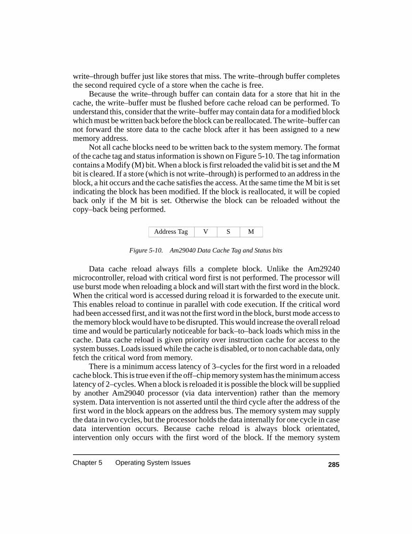
285Chapter 5 Operating System Issues
write–through buffer just like stores that miss. The write–through buffer completesthe second required cycle of a store when the cache is free.
Because the write–through buffer can contain data for a store that hit in thecache, the write–buffer must be flushed before cache reload can be performed. Tounderstand this, consider that the write–buffer may contain data for a modified blockwhich must be written back before the block can be reallocated. The write–buffer cannot forward the store data to the cache block after it has been assigned to a newmemory address.
Not all cache blocks need to be written back to the system memory. The formatof the cache tag and status information is shown on Figure 5-10. The tag informationcontains a Modify (M) bit. When a block is first reloaded the valid bit is set and the Mbit is cleared. If a store (which is not write–through) is performed to an address in theblock, a hit occurs and the cache satisfies the access. At the same time the M bit is setindicating the block has been modified. If the block is reallocated, it will be copiedback only if the M bit is set. Otherwise the block can be reloaded without thecopy–back being performed.
Figure 5-10. Am29040 Data Cache Tag and Status bits
Address Tag V S M
Data cache reload always fills a complete block. Unlike the Am29240microcontroller, reload with critical word first is not performed. The processor willuse burst mode when reloading a block and will start with the first word in the block.When the critical word is accessed during reload it is forwarded to the execute unit.This enables reload to continue in parallel with code execution. If the critical wordhad been accessed first, and it was not the first word in the block, burst mode access tothe memory block would have to be disrupted. This would increase the overall reloadtime and would be particularly noticeable for back–to–back loads which miss in thecache. Data cache reload is given priority over instruction cache for access to thesystem busses. Loads issued while the cache is disabled, or to non cachable data, onlyfetch the critical word from memory.
There is a minimum access latency of 3–cycles for the first word in a reloadedcache block. This is true even if the off–chip memory system has the minimum accesslatency of 2–cycles. When a block is reloaded it is possible the block will be suppliedby another Am29040 processor (via data intervention) rather than the memorysystem. Data intervention is not asserted until the third cycle after the address of thefirst word in the block appears on the address bus. The memory system may supplythe data in two cycles, but the processor holds the data internally for one cycle in casedata intervention occurs. Because cache reload is always block orientated,intervention only occurs with the first word of the block. If the memory system

286 Evaluating and Programming the 29K RISC Family
latency is 3–cycle or more, the processor does not delay the forwarding of the firstdata word. For single–cycle burst–mode memories, the remaining data words are notdelayed internally by an additional cycle (given 2–cycle first access) unless aload–multiple is being performed. Only accessed data, rather than reloaded datavalues, are sent to the 29K data channel.
Peripheral devices such as a UART can be accessed at physical memorylocations determined by specific system hardware. Because the status and data of anexternal device can change at any time, it is undesirable to cache their contents.Access to these devices is normally accomplished in Supervisor mode. On enteringSupervisor mode the data cache could be disabled by setting the DD bit in the CFGconfiguration register (this happens automatically if the FPD bit is not set in the CFGregister). This may be convenient for assembly level code as the cache may only bedisabled for a short time. Alternatively, assembly code could use LOADLinstructions (which, unlike the Am29240, may cause block allocation) whenaccessing peripherals. The LOADL instruction always accesses off–chip memory.However, if operating system code is implemented in C then it is desirable, forperformance reasons, that the operating system data also be cached. A note ofcaution, when the cache is disabled its contents are retained. Consequently, ifmemory locations, currently cached, are modified while the cache is disabled, thecache will supply out–of–date data when it is reenabled. This must be avoided.
The key word volatile can be used in C to indicate that data should not be held ininternal registers. However, this data may still be cached. Hence, marking datavolatile is insufficient to ensure that it is always accessed from off–chip memory. Asdescribed in the previous Am29240 section, defining the data type to be _LOCKvolatile is one way of instructing the compiler to use only LOADL instructions whenaccessing peripherals. The Am29040 has an alternative; the MMU can be configuredto disable caching of selected memory pages. This means the operating system code(or for that mater User mode code) must run with address translation turned on. WhenTLB reload occurs, the memory management software must ensure the two–bit field(PGM) of the TLB registers is set to “non cachable” for memory addressescontaining mapped peripherals. The PGM field format is shown on Table 5-4.
Table 5-4. PGM Field of the Am29040 Microprocessor TLB
PGM1 PGM0 Effect
0 0 normal (copy–back)
0 1 write–through
1 0 reserved
1 1 non cachable

287Chapter 5 Operating System Issues
Data loads performed to memory locations which are marked non cachable arenot subject to data intervention. There is never any internal delaying of data in casedata intervention occurs late in the access. Hence, the critical word can be accessed ina minimum of 2–cycles –– given a 2–cycle memory system. This requires that a dataregion which is not cached by a processors, also not be cached by any other processor(in a multiprocessor system).
With virtual addressing in use, the MMU can be configured to select awrite–through policy on a per–page bases. The write–through policy ensures thatdata in external memory is always consistent with data held in cache as all loadinstructions are applied to memory (and to the cache if they hit). Selecting this policyfor all memory pages would result in a poorer overall performance compared to thedefault copy–back policy. However, regions of address space may be allocated toperipherals which require immediate update. For example, video memory should bemarked as write–through rather than cachable. There is a definite advantage toaccessing video frame information from the cache when manipulating images.Additionally, system implementations which fail to deal with the additionalhardware signals needed to support bus snooping may use write–through access toassist with cache coherence problems. A write–through policy would only enable anexternal agent to read shared data, it would not be able to modify the data.
To achieve the best performance, application code will likely use the data cachewith copy–back operation selected. However, there are situations when anapplication will prefer write–through cache operation –– at least for portions of thememory space. Memory locations are frequently used to pass data between operatingsystem and application code. If the operating system where to use copy–back datacache operation (the default), there would be a danger that some data blocks(accessed by the operating system) would be cached and their M bit set; later whenreturning to the application, the block may be within a memory page which is markedwrite–through, this would prevent the block being copied–back should the block bereallocated. It is best to run the operating system with address translation turned on.This enables the MMU to control the cache operation for memory pages which arejointly accessed by the operating system and application code. To simplify this task,the configuration register has an Freeze–PD (FPD) bit. When this bit is set thePhysical Data (PD) bit in the CPS registers is not set when the operating system isentered via a trap or interrupt. The FPD bit enables the PD bit to remain unchanged.Thus, if address translation was enabled in the application, it will remain enabledafter a trap or interrupt. The data cache need not be disabled when the operatingsystem is entered. However, the MMU must ensure a consistent cache policy formemory pages which are jointly accessed by operating system and application code.
The Am29040 processor deals with other agents, such as a DMA controller,accessing the same memory by performing bus snooping. Multiprocessor designs,with on–chip caches, are also supported by the snooping protocol. The Shared (S) bit
288 Evaluating and Programming the 29K RISC Family
in the cache tag is used to support the protocol. The S bit becomes set when a write isperformed to an address which causes block reload, and the block is supplied byanother cache –– more on this in the following Cache Consistency section.
The Am29040 processor, unlike the Am29240, does not allocate cache blocksfor data fetched with a LOADM instruction. This prevents needless displacement ofvalid cache blocks when a register stack fill is performed. Block allocation during aLOADM in conjunction with a copy–back policy would have poor performancegiven that the copy–back buffer is only four words deep. The copy–back buffer andthe LOADM instruction would both be competing for access to the system bus.
5.14.3 Cache Locking and Invalidating
Valid data cache blocks can be locked by appropriately setting the DL field ofthe CFG configuration register. The entire cache can be locked or only column 0. If ablock is locked but still invalid, it can be allocated for caching. Critical data can beplaced in the cache by first locking the cache and then loading the required data. Thiseffectively turns the cache into a small fast RAM for critical data. (However, awrite–through policy, if used, will still cause all writes to be duplicated in off–chipmemory). If only column 0 is locked the remaining column 1 will still cache entrieswith a direct–mapping replacement scheme. Typical applications show bestperformance when the cache is not locked but left to the default scheme of cachingthe most recently accessed data.
The cache can be invalidated in a single cycle by issuing an INV or IRETINVtype instruction. All blocks are marked invalid during this process unless the cache islocked. A locked cache can only be marked invalid if it is first disabled beforeinvalidating.
The copy–back policy of the Am29040 makes cache invalidation more difficult.Valid cache blocks which have been modified can not be simply marked invalid.Failure to write–back modified blocks would leave the memory in an out–of–datestate. Because the data cache operates with physical address tags and performs bussnooping, there is very little reason to invalidate the cache. Cache invalidation can besafely performed by using the cache interface registers (CIR and CDR) to examineeach block to determine if the block is valid and if the modified bit (M bit) is set.When set, the block must be written out to memory before an INV type instruction isused.
5.14.4 Cache Consistency
The Am29040 is currently the only processor in the 29K family which containson–chip data cache consistency hardware. Cache consistency becomes an issuewhen there is more than one cache in a multiprocessor system or when a DMA typedevice is also accessing data regions which are cached. When there is more than oneagent trying to access data, it is important that all agents agree upon a single (and
289Chapter 5 Operating System Issues
most recent) value. A solution to this problem is for each processor to make virtualaddress access to the shared memory pages and mark the pages as non cachable.However, unless all memory is marked non cachable the plan would require thatsoftware arrange for data intended for shared memory to appear in a range ofcontiguous non cached memory. There would need to be an agreement with theoperating system that the selected address range was not to be cached. Such amechanism would be undesirable, inflexible, and difficult to retrofit to existingsoftware.
With systems incorporating multiple Am29040 processors, each processor maycache the same memory location. This is desirable, as access to the cache is muchfaster than off–chip access. The processor supports three interface signal pins whichfacilitate “bus watching” for data reads with cache block granularity. The techniquerequires little software support, and existing programs can benefit without anymodifications. The on–chip protocol supporting the interface signals ensures thateach memory access is consistent.
When a load is performed, all processors watching the bus determine if theyhave a currently cached copy of the requested data. If they do, they assert the HITsignal pin. The protocol will enable one cache to identify itself as the owner of thedata. This cache will assert both the HIT and the DI (“data intervention”) signals. Theprocessor requesting the load is satisfied by the intervening cache. The load willcause a block to be allocated with the S bit set in the tag. This indicates the data isshared. The processor can continue to access the data from the cache. Additionally,all processors asserting the HIT signal will realize that another processor is sharingthe data and will set the S bit in their cached copy. If any processor modifies a blocktagged with the same address, that processor will perform a “write broadcast” as aresult of the S bit being set. This does not cause the system memory to be updated, butenables the snooping processors to update their cached copies. A processor assertsthe WBC signal pin during the write broadcast and becomes the owner of the sharedblock. The processor will remain the owner of the block until another processor gainsownership by performing a write broadcast itself. When a processor performs a writebroadcast it checks to see if another processor is asserting the HIT signal, if not thenthe processor realizes it is now the only processor caching the data and therefor clearsthe S bit.
To summarize, bus watching of reloads is used to detect sharing of data. Whendata is shared all caches set the S bit in the cached block. The processor whichsatisfied the block reload (in place of the memory) is the owner of the block and hasthe S and M (modified) bits set in the block tag. Writes to shared data create writebroadcasts on the bus to inform other caches of the change of value. Ownership of ablock is transferred to the processor performing the write broadcast. Cache to cachecommunications via write broadcasts is a lot faster than accessing slower systemmemory.
290 Evaluating and Programming the 29K RISC Family
Bus watching monitors write–through and copy–back of cached data. Memoryregions which are accessed as write–through never have cache blocks which aremodified (that is, their tag M bit is never set). All writes to such regions are performedto the system memory. Caches with matching blocks will update their data when thewrite–through takes place. Only blocks which have been modified get copied backwhen the block is reallocated. When a block is copied–back, other caches will retaintheir clean copies of the shared data. There will now be no owner of the data. Ifanother cache performs a load for the data, no processor will intervene and the datablock will be fetched from memory. The data consistency protocol is some timesreferred to as a “MOESI” protocol (reflecting the five states: Modified, Owned,Exclusive, Shared, and Invalid).
The Am29040 processor supports an optimization for use with binarysemaphores. They are frequently used to enable or disable access to shared resources.A processor can gain exclusive access to a resource via the LOADSET instruction.The instruction atomically loads the value from the semaphore memory location andthen writes the set–value (0xffff,ffff) to the location. The loaded value can then betested; if it was already set, access is disallowed. Access to a shared resource isgranted when a zero semaphore is read. The process of accessing the semaphore witha LOADSET instruction disables allocation of the resource to other requestingagents. When acquiring unset semaphores, the processor maintains exclusive controlof the system bus.
When access is not granted, a processor will, typically, repeatedly access thesemaphore waiting for it to become unset. However, continually polling a memorylocation which is held in shared memory can be a serious performance problem. Toprevent the associated bus activity, the Am29040 can cache binary semaphores. If aprocessor busy–waits, the semaphore traffic is isolated to the processors data cache.Additionally, when a semaphore value is found to be set, further LOADSETinstructions are not granted access to the external bus until the semaphore is cleared.The processor knows the semaphore is set by testing bit–31 of the cached value; insuch case there is no need to perform the SET portion of the LOADSET as thesemaphore is already set. The processor currently holding access to the semaphorewill perform a write broadcast when it releases the shared semaphore. A STORELatomic instruction is used to clear the semaphore value. The STOREL instruction,like a LOADSET to an unset semaphore, has exclusive control of the bus during itsexecution. The mechanism ensures that at any time only one processor can gainaccess to a shared resource.
5.15 SELECTING AN OPERATING SYSTEM
I am often asked by engineers about to start a 29K project, what they shouldlook for when selecting an operating system. There are a number of companiesoffering operating systems with a range of different capabilities; alternatively a
291Chapter 5 Operating System Issues
home–grown system could be constructed. The material covered in this chapter andothers should help in either constructing or selecting a suitable operating system. Iwould certainly advice seriously considering purchasing rather than constructing.The task may be enjoyable but probably more lengthy than most project time tableswill allow. However, for those who insist on building their own operating system,AMD has a collection of useful routines which make a good starting point. ContactAMD 29K customer support for a copy of the code.
There is usually no one right operating system. The choice depends on a numberof criteria which may vary from project to project. The following list presents severalquestions which you need to ask yourself and possibly operating system vendors.You can decide the importance of each item with regard your project requirements.
Are 3–bus family members as well as 2–bus members supported? If theAm29000 or Am29050 processors are to be used, and the data bus andinstruction bus are not to be tied together, then the operating system must beclear about maintaining code and data in separate regions. The Harvardarchitecture, supported by 3–bus memory systems, typically achieves a 20%performance gain over 2–bus memory systems. Additionally, when 3–bussystems are supported, the operating system may require the support of ahardware bridge allowing the instruction memory to be reached (usually withaccess delays) via a data memory access.
Are interruptible SPILL and FILL code supported? By running them withinterrupts disabled the difficulties of performing repair of the register stacksupport registers can be avoided, should they be interrupted. However, theyrequire the support of multi–cycle LOADM and STOREM instructions, whichresults in increased interrupt latency. Additionally, SPILL and FILL supportwith interrupts disabled, results in a larger overhead compared withtrampolining to support routines; thus it is non–optimal as SPILL ing andFILL ing occur a lot more often then their interruption.
Given that SPILL and FILL are interruptible, their operation is interdependentwith the longjmp() library routine and the signal trampoline code. All four ofthese services must coordinate their manipulation of register stack supportregisters if interrupts are to be reliably supported.
Some operating systems support nested interrupts, others do not; without nestedinterrupt support, interrupt latency can be increased. The use of kernel threadsto complete interrupt processing is one way to keep down latency. If interrupthandlers are to be written in a high level language such as C, it may be desirableto support Freeze mode handlers in C. This greatly reduces the interrupt supportoverhead, because the overhead of preparing the register stack for use bynon–leaf procedures is relatively high. Does the operating system under

292 Evaluating and Programming the 29K RISC Family
consideration use interrupt tagwords to support interrupt context caching forFreeze mode handlers?
An interrupt can be configured to generate a task context switch, the new taskbeing responsible for completing interrupt processing. This method has agreater overhead associated with it than processing the interrupt in the contextof the interrupted task. Task context switching requires the register cache to beflushed and reloaded with the incoming task’s register data. A C–level interrupthandler can use the stack cut–across technique to avoid flushing the registercache. Certainly some interrupts must cause task context switching to occur, butit is best to avoid this approach as a general mechanism for dealing withinterrupts. Additionally, if tasks run in User mode, the instruction cache must beflushed on a task context switch. It is best to reduce the number of cache flushesdue to interrupt support.
If the system is to support a high interrupt throughput, then processing interruptswith a Dispatcher will be more efficient. The Dispatcher can execute inassembly level or C level. If C, then the interrupted register stack condition needonly be repaired once before entering the Dispatcher, rather than for everyinterrupt (see section 2.5.6).
Interrupt latency can be reduced if Freeze mode interrupt processing is neverdisabled. For a HIF conforming operating system, the technique was describedin section 2.5.7 (Minimizing Interrupt Latency).
Synchronous context switching times are greatly improved by only restoringthe activation record of the procedure about to start execution. This can only bedone for tasks which were synchronously switched out; but is a better methodthan restoring the register stack to the exact position in use at the time of the taskcontext save.
Many embedded operating systems run tasks in Supervisor mode rather thanUser mode. This gives each task direct access to critical resources, there is noneed to use system calls (which use a trap instruction to enter Supervisor mode)to gain access to restricted resources. Always running in Supervisor mode hasthe additional advantage that the Instruction cache need not be flushed on a taskcontext switch. However, the benefits of memory access protection are typicallyreduced or unavailable with such systems.
Operating systems each have their own system call interface which is usually alittle different from HIF (see Appendix C). However, it may be still useful tohave HIF services available. The HIF services can often be supported bytranslating them into the underlying operating system serves. The High C 29Kand GNU library services generate HIF service calls. These libraries can be usedwith a non–HIF operating system; but care must be taken as library routines

293Chapter 5 Operating System Issues
such as printf() are not reentrant. The OS–boot operating system, most oftenused with HIF conforming library services, does not support task switching, butother operating systems will, and the reentrant library procedure limitations willbecome a problem.
Not all members of the 29K family support floating–point instructions directlyin hardware. It is the operating system’s responsibility to ensure that the desiredfloating–point emulation routines (trapware) are installed. The operatingsystem vendor should also supply the appropriate transcendental libraryservices (sin(), cos(), etc.) for the chosen processor.
Floating–point instruction emulation is typically configured to operate withinterrupts not enabled. This avoids the need to save interrupted floating–pointcontext. However, the addition of floating–point environment saving duringapplication context switching is a requirement for some systems and anunwanted burden for other systems. It is worth knowing the options anoperating system supports in this area.
It is often desirable and less expensive to purchase an operating system inlinkable or binary form, rather than source. This makes it more difficult to makechanges to the operating system code; this can be required to incorporatesupport for specialized peripheral devices. It is best that the operating systemnot consume all of the 32 global registers assigned for operating systems use(gr64–gr95). Additionally, linkable operating system images can use link–timeregister assignment rather than compile time. This enables the user to rearrangethe global register usage and utilize unassigned registers for peripheral supporttasks.
The 29K family has no hierarchical memory management unit policy built intothe hardware. Support of the translation look–aside buffers is left to software.This offers great flexibility, but generates questions about the MMU supportpolicy adopted by the operating system. Even if address translation is notsupported by an operating system, it is still desirable to use the MMU hardware(where available) to support address access protection with one–to–one addresstranslation.
There is a movement in the operating system business, which includes real–timevariants, to support POSIX conforming system calls. It may be worth knowinghow, and to what extent, the operating system vendor plans to support POSIX.
Support for debugging operating system activity and application code is veryimportant. Often operating systems have weaknesses in this area. TheUniversal Debug Interface (UDI) has been influential in the 29K debug toolbusiness. It offers flexibility in debug tool configuration, flexibility and
294 Evaluating and Programming the 29K RISC Family
selection. Debug tools are generally more available for DOS and UNIX basedcross development environments.
5.16 SUMMARY
Typical RISC processors, including the 29K, require more complex systemsoftware. The manageability of such software development is very much a functionof the particular RISC processor implementation. Increased knowledge of how thecompiler utilizes the processor registers is required to achieve best performance. Theavailability of a large number of internal registers leads to improved operationspeeds; although the performance gains are at the cost of a somewhat more complexapplication task context switch.
The use of interrupt processing via lightweight interrupts and signal handlingmethods, along with the relative infrequency of context switching, enable the systemdesigner to implement a supervisor of generally much improved performance,vis–a–vis CISC processors. Fortunately, application developers can make use ofRISC technology without having to solve the supervisor design problemsthemselves, as there are a number of operating system products available.

295
Chapter 6
Memory Management Unit
Address values generated by the program counter and data load and store opera-tions appear on the Am29000 processor address bus. Certain members of the 29Kfamily contain instruction caches, which eliminates the need for the processor to re-quest instructions from external memory when the required instruction can be ob-tained from the cache. However, unless the Memory Management Unit (MMU) is inoperation, address values will flow directly on to the pins assigned to the address bus.
The MMU enables address values to be translated, to some extent, into a differ-ent physical address. This means that the address values generated by a program neednot directly correspond to the physical address values which appear on the chips ad-dress pins. The program generates virtual addresses for data and instructions whichare located in physical memory at addresses determined by the MMU addresstranslation hardware.
With the Am29000 processor, virtual address space is broken into pages of 1Kbyte, 2K byte, 4K byte or 8K byte size. The first page begins at address 0 and subse-quent pages are aligned to page boundaries. The MMU does not modify the loweraddress bits used to address data within a page. For example, with a 4K page size, thelower 12 address bits are never modified. However, the MMU translates the upper 20virtual address bits into a new 20–bit value. The translated upper 20–bits and theoriginal lower 12–bits are combined to produce a 32–bit physical address value.
The use of an MMU enables a program to appear to have memory located overthe complete 32–bit virtual address space (4G bytes). The physical memory systemis, of course, much smaller. Virtually addressed pages are mapped (via addresstranslation) into physical pages located in the available memory, typically 1M to 4Mbytes. A secondary memory is used to store virtually address pages which are not cur-rently located in the physical memory due to its limited size.

296 Evaluating and Programming the 29K RISC Family
The secondary memory is typically a disk. When the MMU identifies the pro-gram’s need to access data stored on a page currently out on disk, it must instruct theoperating system to page–in the required page into the physical memory. The pagemay be located almost anywhere in physical memory, but the address translation ca-pability of the MMU will make the page appear at the desired virtual address ac-cessed by the program. In the process of paging–in from disk, the operating systemmay have to page–out to disk a page currently located in physical memory. In thisway memory space is made available for the in–coming page.
Within the 29K family, the MMU unit is located on–chip, and is constructed us-ing Translation Look–Aside Buffers (TLBs). This chapter describes in detail how theTLB hardware operates, and how it can be used to implement a virtual address capa-bility. The TLBs provide other functions in addition to address translation, such asseparate access permissions for data read, write and instruction execution. These im-portant functions will be explained and highlighted in example code.
6.1 SRAM VERSUS DRAM PERFORMANCE
As already stated, secondary memory is typically disk. However, it is difficult toshow example code relying on disk controller operation. The example code would betoo large and too much time would be spent dealing with disk controller operation.This is not our intention. I have chosen to use SRAM devices for physical memoryand DRAM and EPROM devices have been chosen to play the role of secondarymemory.
SRAM devices are much faster than most DRAM memory system arrange-ments. Thus, by paging the program into SRAM, a very desirable speed gain shouldbe obtained. Certainly the secondary memory capacity is limited to the typically 1Mto 4M bytes made available by the DRAM and EPROM combination. But programswill execute from SRAM alone, which may be limited to as little as 128K bytes. Forlarge programs this is likely to result in SRAM pages being paged out to secondaryDRAM to make space available for incoming pages.
The SRAM will effectively be a memory cache for the secondary DRAM; theAm29000 processor MMU being used to implement a software controlled cachemechanism. The performance difference shown by programs executing from SRAMversus DRAM is large. Figure 6-1 shows the average cycles required per instructionexecution for four well know UNIX utility programs. The influence of memory per-formance on these benchmarks is likely to be similar to that experienced by large em-bedded application programs. The DRAM memory system used is termed 4–1. Thisterminology is used throughout this chapter. In this case it means the memory systemrequires four cycles for a random access and one cycle for a burst–mode access.
Burst–mode enables multiple instructions and data to be accessed consecutivelyafter a single start address has been supplied. The first data or instruction word in theburst suffers the access penalties of a random access, but subsequent accesses are

297Chapter 6 Memory Mangement Unit
much less expensive in terms of access delay cycles. The external memory system isresponsible for generating access addresses after the processor has supplied the startaddress for the burst. This can be simply achieved with an address latch and counter.
0
1
2
3
4
compress diff nroff assembler
Average cycles per instruction
Joint I/D 4–1 DRAM memory system
Separate I/D
Figure 6-1. Average Cycles per Instruction Using DRAM
The Am29000 processor can execute a new instruction every cycle if supportedby the memory system. Figure 6-1 shows that the desired 1 cycle per instruction is farfrom achievable by the utility programs using a 4–1 memory system. Certain mem-bers of the 29K family (the Am29000 and the Am29050 processors) support a 3–busarchitecture. One bus is used for physical address values, and there are separatebusses for instruction and data information. This bus structure allows simultaneousinstruction and data transfer. Once the address bus has been used to supply the startaddress of an instruction burst, the address bus is free for use in random or burst–mode data accesses. Figure 6-1 shows performance values for both separate (sepa-rate I/D), and joint instruction and data (joint I/D) busses. It can be clearly seen thatseparate busses offer a significant performance gain. Figure 6-2 shows the averagecycles per instruction for the same four benchmarks executing on a 2–1 memory sys-tem.
Implementing a 2–1 memory system at 25M Hz processor speeds, in particularobtaining a 2–cycle first access, requires SRAM memory devices. The results onFigure 6-2 show that 1–cycle per instruction is almost achieved when a separateinstruction and data bus is used with 2–1 memory.
29K family members supporting separate busses do not have any means withinthe chip of reading data which is located in instruction memory. If instructions anddata are to be located in the same memory pages, then an off–chip bridge must be

298 Evaluating and Programming the 29K RISC Family
0
1
2
compress diff nroff assembler
Average cycles per instruction
Joint I/D 2–1 SRAM memory system
Separate I/D
Figure 6-2. Average Cycles per Instruction Using SRAM
constructed between the the data and instruction busses. Accessing data located inthe instruction memory system via the bridge connected to the data bus, will requiremore access cycles than accessing data located in the data memory system connectedto the data bus directly. The bridge could support accessing instructions located indata memory, but the performance penalties seem too great to implement. The bridgemechanism is acceptable if used for the occasional read of data located in EPROMattached to the instruction bus. It can also be used for reading, as data, an instructionwhich has caused an execute exception violation.
The construction of two memory systems, one for data and a second for instruc-tions, is undesirable. But it does allow a performance gain. This chapter shall dealwith an example system with a joint I/D. This is because the code example is simpli-fied. A separate I/D memory system would require separate instruction and datamemory caches and associated support data structures. A block diagram of the exam-ple system is shown in Figure 6-3.
Even with a joint I/D memory system it may still be necessary to build twomemory systems to achieve a low number of cycles per instruction. This is because itis difficult to achieve single cycle burst–mode access with current memory devices at25M Hz processor rates. Two memory systems are required and are used alternative-ly. This technique is often called memory system interleaving. One memory systemsupplies words lying on even word boundaries and the second memory system sup-plies words lying on odd word boundaries. In this way each memory system has twiceas many cycles to respond to consecutive memory accesses compared to a singlememory system acting alone.
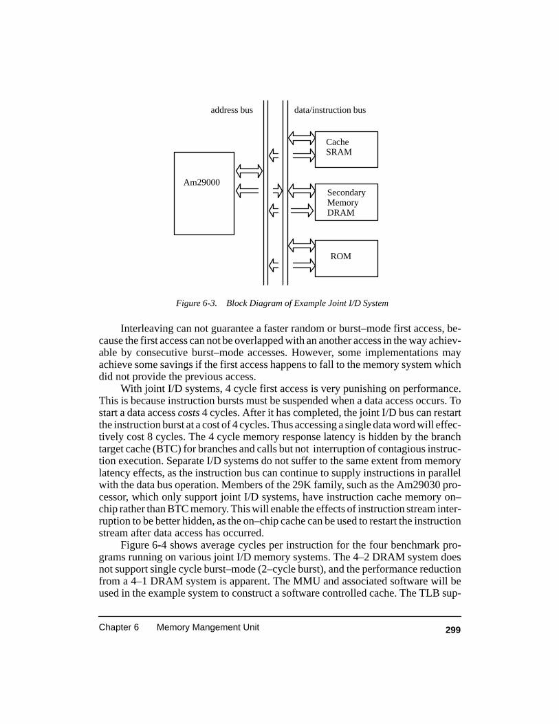
299Chapter 6 Memory Mangement Unit
address bus data/instruction bus
Am29000
CacheSRAM
SecondaryMemoryDRAM
ROM
Figure 6-3. Block Diagram of Example Joint I/D System
Interleaving can not guarantee a faster random or burst–mode first access, be-cause the first access can not be overlapped with an another access in the way achiev-able by consecutive burst–mode accesses. However, some implementations mayachieve some savings if the first access happens to fall to the memory system whichdid not provide the previous access.
With joint I/D systems, 4 cycle first access is very punishing on performance.This is because instruction bursts must be suspended when a data access occurs. Tostart a data access costs 4 cycles. After it has completed, the joint I/D bus can restartthe instruction burst at a cost of 4 cycles. Thus accessing a single data word will effec-tively cost 8 cycles. The 4 cycle memory response latency is hidden by the branchtarget cache (BTC) for branches and calls but not interruption of contagious instruc-tion execution. Separate I/D systems do not suffer to the same extent from memorylatency effects, as the instruction bus can continue to supply instructions in parallelwith the data bus operation. Members of the 29K family, such as the Am29030 pro-cessor, which only support joint I/D systems, have instruction cache memory on–chip rather than BTC memory. This will enable the effects of instruction stream inter-ruption to be better hidden, as the on–chip cache can be used to restart the instructionstream after data access has occurred.
Figure 6-4 shows average cycles per instruction for the four benchmark pro-grams running on various joint I/D memory systems. The 4–2 DRAM system doesnot support single cycle burst–mode (2–cycle burst), and the performance reductionfrom a 4–1 DRAM system is apparent. The MMU and associated software will beused in the example system to construct a software controlled cache. The TLB sup-

300 Evaluating and Programming the 29K RISC Family
ÈÈÈÈÈÈÈÈ
ÈÈÈÈÈÈÈÈ
ÈÈÈÈÈÈÈÈ
ÈÈÈÈÈÈÈÈ0
1
2
3
4
compress diff nroff assembler
Average cycles per instruction
4–2 DRAM Joint I/D memory system
4–1 DRAM
2–1 SRAM
Figure 6-4. Average Cycles per Instruction
port software is based on an Am29000 TLB register format. Members of 29K Familysupporting two TLBs will require some small changes to the example code. The sec-ondary memory shall be a 4–2 or 4–1 DRAM memory system. Programs shall bepaged into a small 2–1 SRAM memory. If the paging activity can be kept to a mini-mum, it is possible that the effective average cycle per instruction will approach thatof SRAM acting alone.
Current costs for DRAM devices are about $5 for 256kx4 DRAMs and $10.50for 32Kx8 SRAMs. At these prices 1M byte of DRAM would cost $40 and 1M byteof SRAM $336. Prices will of course continue to fall on a per–byte basis. However, alarge difference between SRAM and DRAM prices will remain, and SRAM memorysystem costs will remain an obstacle in obtaining the highest system performances. A128K byte SRAM memory cache would cost $42. Using such a cache in conjunctionwith a secondary DRAM memory is a cost effective way of achieving high perfor-mance. Because the Am29000 processor implements TLBs and lightweight inter-rupts (see section 4.3.3) on–chip, it is an ideal processor to implement a softwarecache mechanism.
6.2 TRANSLATION LOOK–ASIDE BUFFER (TLB) OPERATION
The Am29000 processor has a number of special purpose support registers ac-cessible only by the processor operating in Supervisor mode. Special register 2,
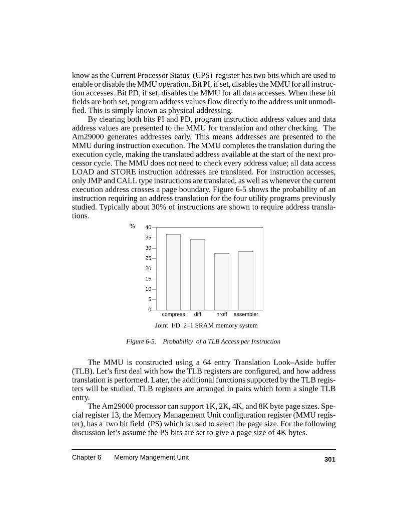
301Chapter 6 Memory Mangement Unit
know as the Current Processor Status (CPS) register has two bits which are used toenable or disable the MMU operation. Bit PI, if set, disables the MMU for all instruc-tion accesses. Bit PD, if set, disables the MMU for all data accesses. When these bitfields are both set, program address values flow directly to the address unit unmodi-fied. This is simply known as physical addressing.
By clearing both bits PI and PD, program instruction address values and dataaddress values are presented to the MMU for translation and other checking. TheAm29000 generates addresses early. This means addresses are presented to theMMU during instruction execution. The MMU completes the translation during theexecution cycle, making the translated address available at the start of the next pro-cessor cycle. The MMU does not need to check every address value; all data accessLOAD and STORE instruction addresses are translated. For instruction accesses,only JMP and CALL type instructions are translated, as well as whenever the currentexecution address crosses a page boundary. Figure 6-5 shows the probability of aninstruction requiring an address translation for the four utility programs previouslystudied. Typically about 30% of instructions are shown to require address transla-tions.
0
5
10
15
20
25
30
35
40
compress diff nroff assembler
Figure 6-5. Probability of a TLB Access per Instruction
%
Joint I/D 2–1 SRAM memory system
The MMU is constructed using a 64 entry Translation Look–Aside buffer(TLB). Let’s first deal with how the TLB registers are configured, and how addresstranslation is performed. Later, the additional functions supported by the TLB regis-ters will be studied. TLB registers are arranged in pairs which form a single TLBentry.
The Am29000 processor can support 1K, 2K, 4K, and 8K byte page sizes. Spe-cial register 13, the Memory Management Unit configuration register (MMU regis-ter), has a two bit field (PS) which is used to select the page size. For the followingdiscussion let’s assume the PS bits are set to give a page size of 4K bytes.

302 Evaluating and Programming the 29K RISC Family
The lower 12 address bits will be unmodified by the MMU translation, they willflow directly to the address pins. The next five address bits (bits 12 to 16) will be usedto select a TLB set. See Figure 6-6 for address field composition. If the page size hadbeen 2K bytes then address bits 11–15 would be used to obtain five bits for TLB setselection. Whatever the page size, five bits are required to select from one of 32 TLBsets. The Am29000 processor has actually 64 TLB entries arranged as two per TLBset.
07152331
Virtual Address Tag Comparison Address offset within Page
11
TLB set
Figure 6-6. TLB Field Composition for 4K Byte Page Size
Each TLB entry contains an address translation for a single page. Therefore theMMU contains translations for a maximum 64 pages. It is possible the address re-quiring translation does not have a match with any of the current TLB entries, but thiswill be discussed later. The virtual address space is divided into 32 sets of equal sizedpages (known as sets 0 to 31). Page 0 starting at address 0 belongs to set 0. Page 1belongs to set 1 and so on. Pages 32, 64 and many more also belong to set 0. Andlikewise page 31, 63 and more belong to set 31. All addresses falling on pages whichare members of the set must obtain an address translation from the TLB entreeswhich are associated with the set. This is know as Set Associative Translation. If apage address could be translated by an entry in any TLB, then the translation tech-nique is known as Fully Associative.
Compared to full associative mechanisms, set associative translation requiresless chip area to implement than full associative mechanisms, and can more easilyoperate at higher speeds. However, there are still many pages which compete witheach other to get their address translation stored in a TLB assigned to the associatedTLB set. For this reason the Am29000 processor supports two TLB entries per set.This is often expressed as “two columns per set”. A page associated with a particularset can have its address translation located in any of the two possible TLB entries.This leads to the title: Two–way Set Associative Translation.
To determine which TLB entry has a valid entry for the page currently beingtranslated, the upper address bits, 17–31 in our 4K byte page example, are comparedwith the the VTAG filed in the TLB entry. The VTAG contains the correspondingupper bits for the TLB entries current translation. If a mach occurs, and other TLBpermission bit field requirements are also satisfied, then the TLB RPN field suppliesthe upper address bits for the now translated physical address. In our 4K page exam-ple the RPN (Real Page Number) field would supply upper address bits 12 to 31,

303Chapter 6 Memory Mangement Unit
which when combined with the page, offset bits 0 to 11, produce a 32–bit physicaladdress. See Figure 6-7 for a block diagram of the TLB layout.
Figure 6-7. Block Diagram of Am29000 processor TLB Layout
this entry a member of set 0
this entry a member of set 1
this entry a member of set 31
TLB Column 0 TLB Column 1
this entry a member of set 0
this entry a member of set 1
this entry a member of set 31
TLB entries are constructed from fields requiring 64–bit storage. This results in128 TLB registers supporting the 64 TLB entries (32 sets 2–ways per set). Two TLBregisters are required to describe a TLB entry. The first TLB register holds entry word0 and a second register holds entry word 1. Figure 6-8 shows the TLB register layout.
Now that the address translation mechanism has been discussed, the TLB entryfields can be examined in more detail. The VTAG and RPN fields have already been
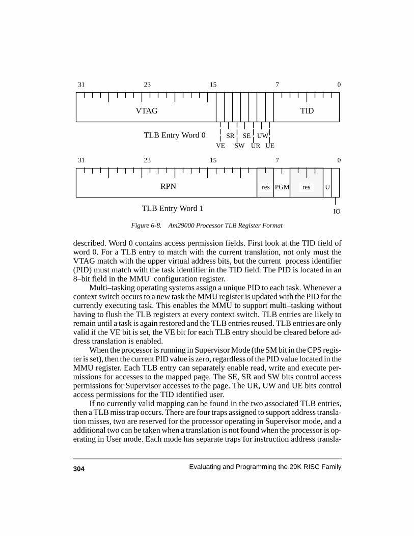
304 Evaluating and Programming the 29K RISC Family
07152331
07152331
TLB Entry Word 1
TLB Entry Word 0
VTAG TID
RPN PGM Ures res
SR SE UW
SW UR UEVE
Figure 6-8. Am29000 Processor TLB Register Format
IO
described. Word 0 contains access permission fields. First look at the TID field ofword 0. For a TLB entry to match with the current translation, not only must theVTAG match with the upper virtual address bits, but the current process identifier(PID) must match with the task identifier in the TID field. The PID is located in an8–bit field in the MMU configuration register.
Multi–tasking operating systems assign a unique PID to each task. Whenever acontext switch occurs to a new task the MMU register is updated with the PID for thecurrently executing task. This enables the MMU to support multi–tasking withouthaving to flush the TLB registers at every context switch. TLB entries are likely toremain until a task is again restored and the TLB entries reused. TLB entries are onlyvalid if the VE bit is set, the VE bit for each TLB entry should be cleared before ad-dress translation is enabled.
When the processor is running in Supervisor Mode (the SM bit in the CPS regis-ter is set), then the current PID value is zero, regardless of the PID value located in theMMU register. Each TLB entry can separately enable read, write and execute per-missions for accesses to the mapped page. The SE, SR and SW bits control accesspermissions for Supervisor accesses to the page. The UR, UW and UE bits controlaccess permissions for the TID identified user.
If no currently valid mapping can be found in the two associated TLB entries,then a TLB miss trap occurs. There are four traps assigned to support address transla-tion misses, two are reserved for the processor operating in Supervisor mode, and aadditional two can be taken when a translation is not found when the processor is op-erating in User mode. Each mode has separate traps for instruction address transla-

305Chapter 6 Memory Mangement Unit
tion and data address translation. A subsequent section describes the process of tak-ing a trap.
Two additional traps are assigned to Supervisor and User mode protectionviolations. These occur when a TLB entry has a valid entry but the permission fieldsdo not allow the type of access being attempted. For example unless the UW bit is seta User mode process can not write to the mapped page, even if all other TLB entryfields indicate a match with the translation address.
Now examine the bit fields of word 1. The IO bit is little used, it enables a virtualaddress to be associated with a physical page in I/O space. The U bit is maintained bythe Am29000 processor. Whenever a TLB set is used in a valid translation the U bitassociated with the set is updated to indicate which of the two TLB entries was used.In other words, the U bit selects the column within the set. The U bit is used to supplythe most significant bit in the least–recently used (LRU) register. Special register 14has a 6–bit field which is updated whenever an address translation fails and a TLBaccess trap occurs. The lower 5–bits of the LRU register are loaded with the TLB setnumber. Thus the LRU register supplies to the trap handler a recommendation forTLB entry replacement. The trap handler typically builds a new valid TLB entry atthe recommended location before execution of the interrupted program is continued.
The 2–bit PGM field is not assigned a task by the Am29000 processor, these bitsare placed on the PGM[1:0] out put pins when a translation occurs. Developers canplace any information they wish in the PGM bits. These bits are particularly usefulfor multiprocessor applications when one processor wishes to signal other processorsabout page cache–ability information.
All data accesses have their translated address and corresponding PGM valuepresented on the the chip pins in the cycle following the cycle executing the LOAD orSTORE instruction. Pages containing instructions have their corresponding PGMbits presented to the chip bins when a jump or call to an address within the page firstoccurred. However, if the target of the jump or call is found in the on–chip instructioncache and the address bus is currently in use when jump or call instruction is inexecute, the PGM bits for the target instruction page will not be presented to the chipPGM[1:0] bins.
In this chapter, the software controlled cache code example shall use the PGMbits to store page–lock and page–dirty information in bits PGM[0] and PGM[1], re-spectively.
6.2.1 Dual TLB Processors
Newer microprocessor and microcontroller members of the 29K family do nothave the full complement of 64 address translations cached in their TLB. A smallerTLB size of 16 entries enables valuable silicon space to be used for on–chip func-tions; such as peripherals. To support the smaller number of TLB entries, the maxi-mum page size has been increased from 8k bytes to 16M bytes. This enables a large
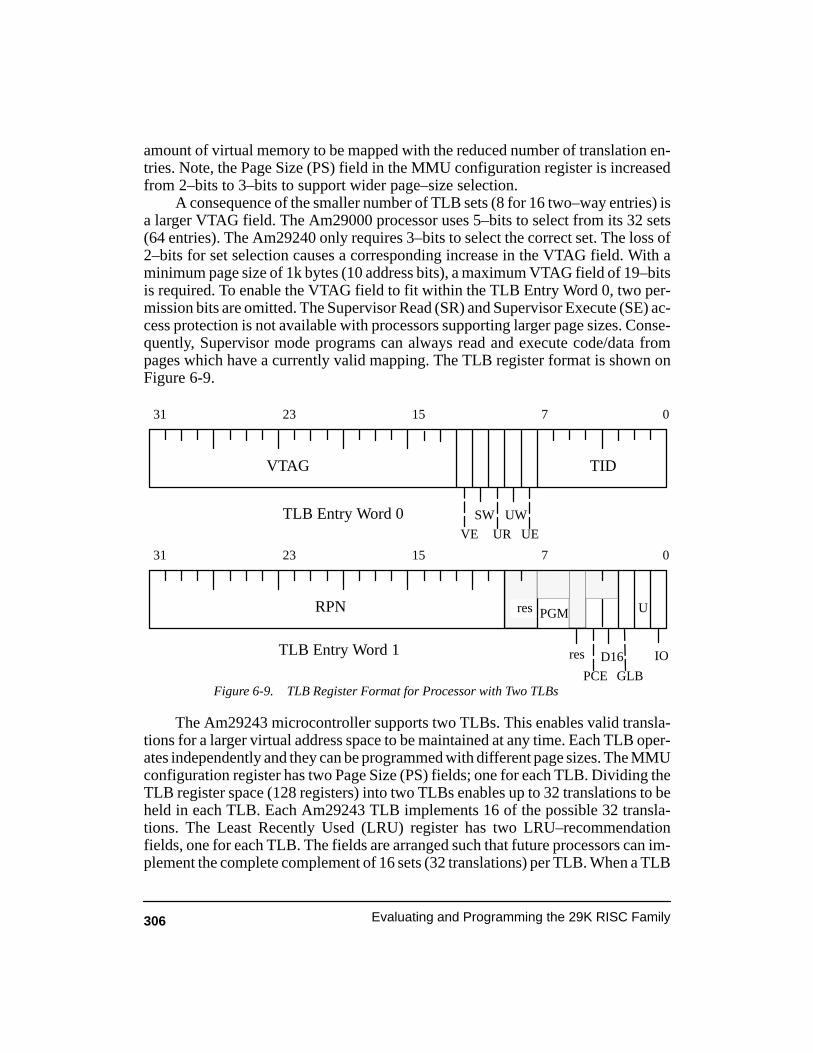
306 Evaluating and Programming the 29K RISC Family
amount of virtual memory to be mapped with the reduced number of translation en-tries. Note, the Page Size (PS) field in the MMU configuration register is increasedfrom 2–bits to 3–bits to support wider page–size selection.
A consequence of the smaller number of TLB sets (8 for 16 two–way entries) isa larger VTAG field. The Am29000 processor uses 5–bits to select from its 32 sets(64 entries). The Am29240 only requires 3–bits to select the correct set. The loss of2–bits for set selection causes a corresponding increase in the VTAG field. With aminimum page size of 1k bytes (10 address bits), a maximum VTAG field of 19–bitsis required. To enable the VTAG field to fit within the TLB Entry Word 0, two per-mission bits are omitted. The Supervisor Read (SR) and Supervisor Execute (SE) ac-cess protection is not available with processors supporting larger page sizes. Conse-quently, Supervisor mode programs can always read and execute code/data frompages which have a currently valid mapping. The TLB register format is shown onFigure 6-9.
07152331
07152331
TLB Entry Word 1
TLB Entry Word 0
VTAG TID
RPN U
res
SW UW
VE UR UE
Figure 6-9. TLB Register Format for Processor with Two TLBs
IOD16
PCE GLB
res PGM
The Am29243 microcontroller supports two TLBs. This enables valid transla-tions for a larger virtual address space to be maintained at any time. Each TLB oper-ates independently and they can be programmed with different page sizes. The MMUconfiguration register has two Page Size (PS) fields; one for each TLB. Dividing theTLB register space (128 registers) into two TLBs enables up to 32 translations to beheld in each TLB. Each Am29243 TLB implements 16 of the possible 32 transla-tions. The Least Recently Used (LRU) register has two LRU–recommendationfields, one for each TLB. The fields are arranged such that future processors can im-plement the complete complement of 16 sets (32 translations) per TLB. When a TLB

307Chapter 6 Memory Mangement Unit
miss occurs both LRU fields are update. Support software must decide which LRUfield to use and consequently which TLB to update. If the TLBs are allocated to dif-ferent address regions, the miss address can be used to select the appropriate field.
TLB Entry Word 1 has an additional entry compared with the Am29000 registerformat –– the Global Page (GLB) bit; when set, the mapped page can be accessed byany processes regardless of its process identifier (PID). This can be very useful whendealing with regions of shared code or data. Multiple processes can accessed, say, ashared library, without each process having to have valid translation entries for thememory pages containing the shared information
The Am29040 2–bus processor also supports two TLBs. The TLB register for-mat is the same as used with the Am29240 microcontroller. However, there are anumber of additional fields implemented in Entry Word 1. The width of data bus usedfor external memory accesses can be reduced to 16–bits if the D16 bit is set. Whenset, a 32–bit data object is accessed via two 16–bit accesses. The D16 bit simplifiesaccess to memory or other device which must be accessed with a 16–bit width for-mat. The PCE bit enables parity checking for the mapped page. Parity is odd or evendepending in the POE bit in the Configuration Register (CFG).
Table 6-1. PGM Field of the Am29040 Microprocessor TLB
PGM1 PGM0 Effect
0 0 normal (copy–back)
0 1 write–through
1 0 reserved
1 1 none cachable
With virtual addressing in use, the Am29040 TLB entries enable a data cachemaintenance policy to be selected on a perpage bases (see Table 6-1). The defaultcopy–back policy generaly achieves the highest performance. When the MMU is notin use (physical addressing) a copy–back policy is applied for cached data. See sec-tion 5.14.2 for more details about Am29040 data cache policy. Note, when the D16bit is set, the access is considerd non cacheable.
The example code presented in this chapter for a software controlled cache isbased on the Am29000–type TLB register format. To make the code work with anAm2924x or Am29040 processor would require some small changes. The code se-quences requiring modification would be in the construction of TLB entry Word 0and Word 1. This does not detract from the value of the example code.
6.2.2 Taking a TLB Trap
The address translation performed by the MMU is determined by the trap han-dler routines which are used to update the TLB registers. When the current processorstatus register bits PD and PI are both clear, enabling the MMU hardware for both
308 Evaluating and Programming the 29K RISC Family
data and instruction address translation, the DA and FZ bits in the CPS register mustalso be cleared. Clearing these bits disables Am29000 special register freezing andenables traps to be taken.
When the MMU does not contain a match for the current address translation, atrap is taken by the processor. This also happens for valid translations not meetingpermission requirements. The software executed by the trap handler must construct aTLB entry for the failing address from page table entries (PTEs) stored in memory.The TLB registers simply act as a cache for the currently–needed translations storedin off–chip data memory.
Many CISC–type processors have algorithms in the chip microcode for auto-matically updating the MMU hardware from more extensive data located in externaldata memory. Because the Am29000 does not implement this function in hardware,the user is free to construct a software algorithm for TLB reloading which best suitsthe memory management architecture. This increased flexibility outweighs any re-duction in TLB register reload time that may occur for some configurations. Theflexibility is what makes possible the software controlled cached described later.
When the Am29000 takes a trap the processor enters Supervisor mode with fro-zen critical support registers. This is known as Freeze mode. A more complete ex-planation is given in Chapter 4 (Interrupts and Traps). The frozen special registersdescribe the state of the processor at the time of the address translation failure. Ex-amining these registers enables the trap handler software to determine the necessaryaction and eventually restart the instruction in execute when the trap occurred. Afterthe trapware routines have constructed the required TLB entry, the faulting instruc-tion will be able to complete execution.
Later sections will deal with the trapware in detail for the example software con-trolled cache system. The interesting details of the trapware will be covered then.Since the code is memory architecture specific, the operation of the software con-trolled cache needs to be discussed first. This discussion is in the later section entitledSoftware Controlled Cache Memory Architecture (section 6.4).
6.3 PERFORMANCE EQUATION
Performance has been considered in terms of average number of cycles perinstruction execution. This is a useful metric when considering memory system ar-chitectures. Figure 6-1, Figure 6-2 and Figure 6-4 give average cycles per userinstruction execution (AC/I). However, if a TLB miss occurs during instructionexecution, a number of Supervisor mode trapware instructions will be required toprepare the TLB registers before the user’s code can continue. If TLB trapware is ac-tivated in support of too many instructions, then the effective number of cycles re-quired per application instruction will increase.
The effective average cycles per instruction is given by: Aeffective = P AC/I whereAC/I is the average number of cycles per instruction for the program running in physi-

309Chapter 6 Memory Mangement Unit
cal mode, without the MMU in operation. The multiplying factor, P, determines howmuch performance is reduced by the use of the MMU hardware. The value of P isgiven by:
Pmiss Tcycles1 +
AC/I
P =PTLB/I
We shall look at the terms of this equation individually to determine their effect.Term PTLB/I is the probability an instruction shall cause a TLB access. Figure 6-5showed average figures for PTLB/I observed with the four benchmark programs ex-amined. Given that a TLB access occurs, we are then interested in the probability thatan entry is not found and a miss trap is taken. This conditional probability is given byterm Pmiss, and Figure 6-10 shows average Pmiss values for the four benchmark pro-grams running on the software controlled cache system .
ÈÈÈÈÈÈÈÈ
0
1
2
3
4
1k 2k 4k 8k
%
compress
nroff
assembler
diff
directly mappedpage size (bytes)
Figure 6-10. TLB Miss Ratio for Joint I/D 2–1 SRAMSystem
What matters at present is we observe that TLB miss rates increase as we de-crease page size. This is expected because smaller page sizes mean a smaller portionof the program’s pages have mappings currently cached in the TLB registers. Giventhat the Am29000 processor has a fixed number of TLB entries, it is best to have largepage sizes if TLB misses are to be reduced. However, the better granularity of smallpage sizes may lead to better physical memory utilization. An additional consider-ation is the size of pages transported from secondary memory such as disk or networkconnections. Secondary memory communication may be improved by better com-munication efficiencies. These efficiencies may be achieved with larger page sizes.

310 Evaluating and Programming the 29K RISC Family
0600
12001800240030003600420048005400
1k 2k 4k 8k
assembler
nroff 4–1 DRAM with 128 page 2–1 cache
page size
Figure 6-11. Average Cycles Required per TLB Miss
The final term of the Tcycles equation is the average number of cycles required toprocess a TLB miss. Figure 6-11 shows values for the four benchmark programs run-ning on the cache system. When a TLB miss occurs for a page which is not currentlylocated in the physical memory but in secondary memory, a large number of proces-sor cycles is required to first transfer the page from secondary memory to physicalmemory and then build a valid TLB entry. As the page size increases the TLB misstrap handler execution time increases substantially.
The product, PTLB/I Pmiss Tcycles gives the average number of cycles overheadadded to each application instruction in order to support the MMU operation. Afterstudying the software cache memory architecture, the effective number of cycles perinstruction achieved will be reexamined and compared with the non–cache memoryarchitecture performance.
6.4 SOFTWARE CONTROLLED CACHE MEMORY ARCHITECTURE
By studying a software controlled cache mechanism we can achieve three ob-jectives: First, a better understanding of the non–TLB–cached page–table layout. Se-cond, further understanding of TLB trapware implementation detail.Thirdly, anawareness of software controlled cache benefits.
When a TLB miss occurs, the trap handler must determine the replacement TLBentry data. It does this by indexing a table of Page Table Entries (PTEs). Each PTEcontains information on how to map a physical page into its corresponding secondarymemory page. In our example system, the physical memory is SRAM and the sec-ondary memory is DRAM. In fact, the secondary memory is physically addressable,

311Chapter 6 Memory Mangement Unit
but the execution of all programs from within the limited sized SRAM cache will beattempted, and the DRAM will only be accessed when a page–to or page–from sec-ondary memory needs copying.
There are many different PTE table arrangements. Some systems have multiplelayers of PTEs, where a higher level PTE points to tables of lower level PTEs. In mul-ti–tasking systems, each task may have its own table of PTEs. And if the Supervisorcode also executes with address translation, then it may also have a table of PTEs. Tosimplify our example system, we will assume the supervisor always runs in physicalmode, and there is a single table of PTEs shared by all User mode programs. To evalu-ate the system performance, only single User mode tasks will be run, in particular thenroff and assembler utility programs.
PTEs need not have the same structure as TLB entries. They typically do not.This enables the memory management system to keep additional page information inmemory and only cache critical data in the TLB registers. In addition it may be pos-sible to compact information into a smaller PTE structure, which results in a substan-tial space saving in systems which keep extensive PTE tables permanently in physi-cal memory (in our case SRAM). For the example system, PTEs shall have exactlythe same format as TLB entries. The method has the benefit that TLB entries can beloaded from PTE memory location directly without additional processor cycles be-ing expended in reformatting.
The PTE format will be 4–way set associative. The number of sets shall be lim-ited by the amount of available SRAM cache memory, but a lower limit of 32, estab-lished by the Am29000, is required. Given a minimum page size of 1K bytes, theSRAM can not be smaller that 128K bytes (1K x 4 x 32). If the number of PTE sets isgreater than 32, then the cache has more set resolution than the TLBs. In this case aTLB set caches entries for more than one PTE set, and the TLB VTAG field has moreaddress resolution than the PTE VTAG field requires.
Each TLB entry indicates how the user’s virtual address is mapped into anSRAM page number (given by the TLB RPN entry). The PTE entries must have amapping relationship with DRAM memory pages and SRAM memory pages. Theentries use the PTE RPN field to store the DRAM page number. PTEs also have amapping relationship with SRAM pages. This enables the memory page maintainedby the PTE to be moved between SRAM and DRAM. The PTE SRAM mapping issimple. PTEs and SRAM pages are stored consecutively in memory, as are SRAMpages. Given the PTE address, the corresponding SRAM page address can be foundby determining the PTE address displacement from the PTE table base. The PTE dis-placement, multiplied by the page size, will locate the SRAM page relative to thebase address of SRAM pages. Figure 6-12 outlines the system.
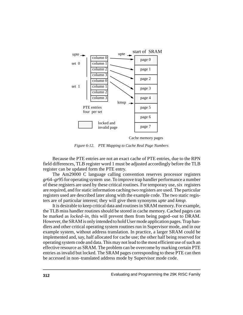
312 Evaluating and Programming the 29K RISC Family
column 0
column 1
column 2
column 3
page 1
page 2
page 3
page 5
page 6
column 0
column 1
column 2
column 3
PTE entriesfour per set
Cache memory pages
start of SRAM
page 4
page 0set 0
set 1
page 7
Figure 6-12. PTE Mapping to Cache Real Page Numbers
upte upte
kmsp
locked andinvalid page
Because the PTE entries are not an exact cache of PTE entries, due to the RPNfield differences, TLB register word 1 must be adjusted accordingly before the TLBregister can be updated form the PTE entry.
The Am29000 C language calling convention reserves processor registersgr64–gr95 for operating system use. To improve trap handler performance a numberof these registers are used by these critical routines. For temporary use, six registersare required, and for static information caching two registers are used. The particularregisters used are described later along with the example code. The two static regis-ters are of particular interest; they will give them synonyms upte and kmsp.
It is desirable to keep critical data and routines in SRAM memory. For example,the TLB miss handler routines should be stored in cache memory. Cached pages canbe marked as locked–in, this will prevent them from being paged–out to DRAM.However, the SRAM is only intended to hold User mode application pages. Trap han-dlers and other critical operating system routines run in Supervisor mode, and in ourexample system, without address translation. In practice, a larger SRAM could beimplemented and, say, half allocated for cache use; the other half being reserved foroperating system code and data. This may not lead to the most efficient use of such aneffective resource as SRAM. The problem can be overcome by marking certain PTEentries as invalid but locked. The SRAM pages corresponding to these PTE can thenbe accessed in non–translated address mode by Supervisor mode code.

313Chapter 6 Memory Mangement Unit
Since the PTE table is frequently accessed by TLB trapware, it is important thatquick access to the table is supported. For this reason register upte is initialized topoint to the base of the PTE table, and the table is located in the first SRAM page. OneSRAM page can contain 32 sets of PTE data. In multi–tasking systems, with eachtask having its own PTE table, the upte value is normally stored in a per–task datastructure know as the Process Control Block (PCB), and the upte register is updatedfrom the PCB data at each context switch.
The Am29000 takes traps very quickly, without expending a number of internalprocessor cycles preparing an interrupt processing context for the processor. This ad-vantage over typical CISC processor operation enables the Am29000 to process thetrap quickly in Freeze mode and return to the user’s program. It is the Freeze modeprocessing capability of the Am29000 that makes a soft cache mechanism attractive.However, TLB miss handlers can not always complete their handling quickly inFreeze mode code. In such cases they must signal the operating system to continuewith further processing, Freeze mode is departed, and Supervisor mode with freezedisabled is entered. Before Freeze mode can be exited, the frozen special registersmust be stored on a Supervisor mode memory stack. They will have to be restoredfrom this stack once the operating system completes the TLB miss processing. Theoperating system stack is located on page 4, which is in a different set from the PTEtable. Operating system accessible register kmsp is used as a stack pointer.
Using the cache architecture described, the nroff and assembler utilities wereobserved running in a 128 page SRAM based system. The page–in activity is shownon Figure 6-13. It appears the two programs were too large to execute in 128K byteSRAM (1K byte page size). The paging activity is at a minimum with a 256K bytecache (2K byte page size). It is possible the increased paging activity is due to cachesets being only 4–way. In the case of nroff, it is more likely the page replacement al-gorithm was having difficulty in keeping the desired pages in the cache for such alarge program.
As page sizes get larger, the probability of a TLB miss diminishes. Since thecache gets larger for a given SRAM of fixed number of pages, expect the probabilityof a page–in to increase as page size increases. Reflecting the fact that with largecaches, a TLB miss causes a page–in and the TLB maintains a cached entry for thepermanently resident page. Figure 6-14 gives the probability of a page–in given aTLB miss has occurred.
With the nroff utility, the probability actually reduces when the page size is in-creased from 1K byte to 2K byte. This is because of the cache–thrashing occurringwith the 128K byte cache used with the 1K byte page size.
6.4.1 Cache Page Maintenance
The example software controlled cache system only supports User mode ad-dress translation. This means Supervisor mode TLB miss handlers will not be consid-
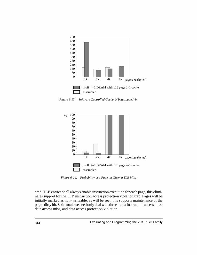
314 Evaluating and Programming the 29K RISC Family
070
140210280350420490560630700
1k 2k 4k 8k
assembler
nroff 4–1 DRAM with 128 page 2–1 cache
page size (bytes)
Figure 6-13. Software Controlled Cache, K bytes paged–in
0102030405060708090
100
1k 2k 4k 8k
Figure 6-14. Probability of a Page–in Given a TLB Miss
assembler
nroff 4–1 DRAM with 128 page 2–1 cache
%
page size (bytes)
ered. TLB entries shall always enable instruction execution for each page, this elimi-nates support for the TLB instruction access protection violation trap. Pages will beinitially marked as non–writeable, as will be seen this supports maintenance of thepage–dirty bit. So in total, we need only deal with three traps: Instruction access miss,data access miss, and data access protection violation.

315Chapter 6 Memory Mangement Unit
The Am29000 has 65 global registers (gr1, gr64–gr127), of these 32 are re-served for operating system use only (gr64–gr95). To improve the performance ofthe trapware, several of the operating system registers have been assigned TLB han-dler support functions. The following code uses register synonyms, so the actual reg-ister assignments can be easily changed.
.reg it0,gr64 ;Freeze mode
.reg it1,gr65 ;temporary regs
.reg it2,gr66
.reg it3,gr67
.reg kt0,gr68 ;temporary regs
.reg kt1,gr69
.reg kmsp,gr93 ;supervisor M–stack
.reg upte,gr95
The code shown within this chapter makes use of a number of macros for push-ing and popping special registers to an external memory stack. These macros, push ,pushsr, pop and popsr, were described in section 3.3.1 (Useful Macro–Instructions).
The example code can be used to construct a cache of various number of PTEentries (ways or columns) per set, and total number of sets. The constant definitionsshown below are used to control the cache size.
.equ PGSIZE,10 ;Page size
.equ C_SETS,6 ;cache sets
.equ C_COLUMNS,2 ;columns per sets
.equ WSIZE,512 ;window size
.equ SIG_ICMISS,1 ;signal I–miss
.equ SIG_DCMISS,3 ;signal D–miss
.equ SIG_PROTECT,5 ;signal W–protect
.equ CTX_CHC,3*4 ;context offset
.sect cache,bss
.use cachecache_adds:
.block (1<<PGSIZE)*(1<<C_SETS)*(1<<C_COLUMNS)
The operating system code, which is not shown, is responsible of initializingsupport registers, kmsp, and upte. It must also mark the PTEs locked and invalid forany SRAM pages which are not to be used for caching, but by the operating system.The example code uses pages 0 and 4 to store performance critical support data.
6.4.2 Data Access TLB Miss
When a read or write data access occurs for a page whose translation from virtu-al to physical address is currently not in the TLB registers, a TLB miss is taken. Thiscauses execution to vector to trap number 9. The address of the trapware handler,UDTLBMiss , is at location 9 in the vector table. A miss may occur because the ac-

316 Evaluating and Programming the 29K RISC Family
cessed page is currently not in the cache, or, more importantly, because the PTE map-ping the cached page is currently not cached by the TLB registers. The PTEs for theappropriate set must be scanned to determine if the page is in the cache.
When a trap is taken, the Am29000 processor special support registers are fro-zen, their contents report the state of the processor at the time of the trap. Special reg-ister CHA contains the virtual address for the failing data access. Using the CHA val-ue, the cache set is determined and the 4 PTE columns assigned to the set are scanned.The PTE valid bit must be set and the PTE VTAG field must match with the upper bitsof the CHA address for a match to be found. Note, the example code does notcompare the TID field; this would be necessary if the cache were supporting a multi–tasking operating system.
UDTLBmiss:mfsr it0,chaconst kt1,SIG_DCMISS ;signal numbersrl it2,it0,PGSIZE ;select cache setand it2,it2,(1<<C_SETS)–1sll it2,it2,3+C_COLUMNSadd it2,it2,upte ;adds of 1st PTE
;scan_columns:
srl it0,it0,PGSIZE+5sll it0,it0,PGSIZE+5const kt0,(1<<C_COLUMNS)–1
next_column:jmpt kt0,not_cached sub kt0,kt0,1 ;dec column countload 0,0,it1,it2 ;load word 0add it2,it2,8 ;next PTE entrysll it3,it1,31–14 ;test VE–bitjmpf it3,next_column srl it3,it1,PGSIZE+5;mask PTE VTAGsll it3,it3,PGSIZE+5cpeq it3,it0,it3 ;compare VTAGjmpf it3,next_column mfsr it3,LRUsub it2,it2,4 ;adds word 1
If a PTE is found in the set which matches with the CHA address, then the TLBentry of the associated set, selected by the LRU register, is updated with the contentsof the matching PTE. Field RPN of word 1 of the PTE is not filled with the secondarymemory (DRAM) page number taken from the PTE, but with the page number of theSRAM cache page.
in_cache:;Word 0 in it1,it2 points to PTE word 1
load 0,0,it0,it2 ;load word 1mttlb it3,it1 ;assign Word 0add it3,it3,1and it0,it0,0xc1 ;mask out RPN

317Chapter 6 Memory Mangement Unit
sub it1,it2,upte ;set offset;srl it1,it1,3 ;set index;sll it1,it1,PGSIZE ;cache page offsetadd it1,it1,upte ;cache RPNor it0,it1,it0 ;or in cache RPNmttlb it3,it0 ;assign Word 1iret
When the required page is found in the cache, the TLB handler executes veryquickly without ever leaving Freeze mode. After the TLB entry has been updated anIRET instruction causes execution to be restarted from the state defined by the frozenspecial registers. The trapware is arranged so the most frequently occurring eventsare processed first and suffer the lowest support overhead. However, if the page is notfound in the cache (no matching PTE) then the trapware must call on the operatingsystem to complete the necessary processing. It does this by sending a signal. Thecode following label not_cached pushes the contents of the special registers as wellas other signal information onto a signal frame on the Supervisor memory stack.Execution is then forced to continue in Supervisor mode with non–translated addres-sing at tlb_sig_handler. The signal frame shall be used to repair the special registersafter the higher level operating system support code has completed.
not_cached:;Send a signal to the operating system
push kmsp,kt1 ;push signal numberpush kmsp,gr1 ;push gr1push kmsp,rab ;push rabconst it0,WSIZEsub gr1,rfb,it0 ;set gr1=rfb–WSIZEsub rab,rfb,it0 ;set rab=rfb–WSIZEpushsr kmsp,it0,pc0 ;push pc0pushsr kmsp,it0,pc1pushsr kmsp,it0,pc2pushsr kmsp,it0,chapushsr kmsp,it0,chdpushsr kmsp,it0,chcpushsr kmsp,it0,alupushsr kmsp,it0,ops ;push ops
;push kmsp,tav ;push tavcpeq tav,kt1,SIG_ICMISSjmpt tav,i_miss mfsr tav,pc1 ;pass address mfsr tav,cha
;i_miss:
mtsrim chc,0 ;cancel load/storemtsrim ops,0x70 ;set PD|PI|SM
;const it1,tlb_sig_handlerconsth it1,tlb_sig_handleradd it0,it1,4 ;trampoline signalmtsr pc1,it1 ; handler

318 Evaluating and Programming the 29K RISC Family
mtsr pc0,it0iret
The signal frame has a signal number field which is used to report the type ofTLB trap which occurred. The layout of the frame is given in Figure 6-15. Globalregister tav (gr121) is used to pass the address causing the trap to occur. For a TLBdata miss, the address is already contained in the CHA register, but copying it to tav isconvenient because the signal handler code is also shared by other routines.
signal number
PC0
PC1
PC2
CHA
CHD
CHC
ALU
OPS
tav
gr1
rab
TLB signal Frame
kmsp
supervisormemorystack, higher ad-dresses at top offigure
Figure 6-15. TLB Signal Frame
6.4.3 Instruction Access TLB Miss
Instruction access TLB misses are dealt with in the same way as data access mis-ses. Only the signal number is different and the faulting address is contained in spe-cial register PC1 rather than CHA. Register PC1 contains the address of the instruc-tion in execute at the time of the failing address translation. Since cache pages con-tain both instructions and data, the same set of PTE apply for data and instruction ad-dress values. Via the interrupt vector table, the User mode instruction access trapnumber 8 causes execution to continue at address label UITLBmiss .
UITLBmiss:mfsr it0,pc1const kt1,SIG_ICMISS ;signal numbersrl it2,it0,PGSIZE ;select cache setand it2,it2,(1<<C_SETS)–1sll it2,it2,3+C_COLUMNS;PTE set offsetjmp scan_columns add it2,it2,upte ;adds of 1st PTE

319Chapter 6 Memory Mangement Unit
6.4.4 Data Write TLB Protection
The following signal handler code is responsible for moving pages from sec-ondary DRAM to SRAM cache memory (paging–in). When pages are first paged–inthey are given read and execute permissions only, unless the initial faulting access isdue to a data write. At some time later during program execution, a write to thecached page may occur. When this happens, a data write protection trap is taken, andexecution is vectored to address label tlb_data_prot.
In the same way as a data TLB miss, the associated PTE entries are scanned tofind the matching entry. There must be a matching entry and, in addition, a cachedTLB entry which is disallowing write access. Once the PTE has been found, the CHAaddress value is again used to find the associated TLB entry. Note, the LRU registercan not be used because it is only updated on TLB misses. To find the TLB entry, theVTAG portion of the CHA address is compared with the only two possible TLB en-tries associated with the set.
;A write request to a read–only page has occurred.
tlb_data_prot:mfsr it0,chaconst kt1,SIG_PROTECT ;signalsrl it2,it0,PGSIZE ;select cache lineand it2,it2,(1<<C_SETS)–1sll it2,it2,3+C_COLUMNS;PTE set offsetadd it2,it2,upte ;adds of 1st PTE
;scan:
srl it0,it0,PGSIZE+5;adds VTAGsll it0,it0,PGSIZE+5const kt0,(1<<C_COLUMNS)–1
nxt_column:jmpt kt0,not_cached sub kt0,kt0,1 ;dec column countload 0,0,it1,it2 ;load word 0add it2,it2,8 ;next PTE entrysll it3,it1,31–14 ;test VE–bitjmpf it3,nxt_column srl it3,it1,PGSIZE+5 ;mask PTE VTAGsll it3,it3,PGSIZE+5cpeq it3,it0,it3 ;compare VTAGjmpf it3,nxt_column
; mfsr it3,cha ;find TLB entrysrl it3,it3,PGSIZE–1;get TLB setand it3,it3,0x3emfsr kt0,chasrl kt0,kt0,PGSIZE+5;form adds VTAGsll kt0,kt0,PGSIZE+5mftlb it0,it3 ;read Word 0srl it0,it0,PGSIZE+5;form TLB VTAGsll it0,it0,PGSIZE+5

320 Evaluating and Programming the 29K RISC Family
cpeq it0,it0,kt0jmpt it0,entry_found sub it2,it2,8 ;PTE adds word 0add it3,it3,64 ;Word 0 in set 1
Once the PTE and TLB entries have been found execution continues at labelentry_found. Both entries must now be updated to set the UW bit enabling Usermode write access. In addition, the PGM[1] bit used to keep a record of any datawrites to the SRAM page is also set. This bit, known as the dirty–bit, will be used inthe page–out algorithm. Once the TLB register reporting the access permission faulthas been updated, an IRET instruction is used to restart the program using the con-tents of the still frozen special registers.
entry_found:;Word 0 in it1, it2 points to PTE word 0
const kt1,0x200 ;UW–bitor it1,it1,kt1store 0,0,it1,it2 ;store new word 0mttlb it3,it1 ;assign Word 0
;add it2,it2,4load 0,0,it0,it2 ;load word 1add it3,it3,1or it0,it0,0x80 ;set PGM[1] dirtystore 0,0,it0,it2 ;store new word 1and it0,it0,0xc1 ;mask out RPNsub it1,it2,upte ;set offsetsrl it1,it1,3 ;set indexsll it1,it1,PGSIZE ;cache page offsetadd it1,it1,upte ;cahe RPNor it0,it1,it0 ;or in cache RPNmttlb it3,it0 ;assign Word 1iret
6.4.5 Supervisor TLB Signal Handler
When trapware code is unable to complete the necessary TLB update, for exam-ple, if the corresponding address is for a page not currently in the cache, the operatingsystem receives a signal and information on its memory stack required to continuethe TLB update process. An IRET instruction is used to trampoline to the signal han-dler address tlb_sig_handler. The IRET does not cause the faulting User modeinstruction to restart, because after the frozen special registers are saved on the stack,the PC registers are loaded with the address of the signal handler. Additionally, theOPS status register is modified to cause Supervisor mode with non–translated ad-dress to commence after the IRET, rather than the interrupted User mode with ad-dress translation on.
A small number of support registers were required to support the trapware rou-tines. The higher level signal handler code requires registers for its own operation. It

321Chapter 6 Memory Mangement Unit
is undesirable to use some of the remaining operating system registers in thegr64–gr95 range to support this code. Global registers are a scarce resource and like-ly needed by other critical operating system tasks. The registers used by the trap han-dlers (it0–it3) are by convention used by all Freeze mode handlers, since duringFreeze mode, interrupts are disabled and therefore there are no register access con-flicts. However, the signal handler code runs with interrupts turned on. An interruptoccurring during signal processing would likely use the interrupt temporary registers(it0–it3), and therefor the signal handler must acquire additional registers for its op-eration. It does this by pushing some of the User mode assigned global registers(gr96–gr127) onto the Supervisor stack, just below the signal frame.
;Try and find an empty PTE entry in the column.;Register tav has the offending address.
tlb_sig_handler:push kmsp, gr96 ;get some registerspush kmsp, gr97push kmsp, gr98push kmsp, gr99push kmsp, gr100
;mfsr gr96,tmc ;get random value
;srl gr98,tav,PGSIZE ;select cache setand gr98,gr98,(1<<C_SETS)–1sll gr98,gr98,3+C_COLUMNS;PTE set offsetadd gr98,gr98,upte ;PTE column 0 address
;const gr100,(1<<C_COLUMNS)–1
column_loop:jmpt gr100,page_out and gr96,gr96,((1<<C_COLUMNS)–1)<<3add gr99,gr98,gr96 ;column wrap–aroundload 0,0,gr97,gr99 ;load word 0add gr96,gr96,8 ;next PTE entrysll gr99,gr97,31–14 ;test VE–bitjmpt gr99,column_loop sub gr100,gr100,1 ;dec column count
;sub gr96,gr96,8call gr100,store_locals;destroys gr96 add gr98,gr98,gr96 ;PTE adds of Word 0
page_in: ;Page–in code follows . . .
The four PTE entries associated with the set are then scanned to find an unusedentry (i.e., the VE bit is not set). If all PTEs are marked valid, then execution contin-ues at page_out. Once a empty entry is found a call to routine store_locals is made.This call causes all 128 local registers within the Am29000 processor to be copiedonto the Supervisor memory stack just below the user’s saved global registers. Note,when the set of four PTEs are scanned, a random column in the set is initially se-

322 Evaluating and Programming the 29K RISC Family
lected. This may initially reduce column scan times. After the local registers havebeen made available for signal handler use, execution continues at label page_in.
6.4.6 Copying a Page into the Cache
Once a PTE for the in–coming page has been selected the corresponding SRAMcache page can be easily determined with a little address–based calculation. Words 0and 1 for the TLB entry are now formed and stored in the TLB selected by the LRUregister. The TLB entry is also copied to the PTE location, with the one differencethat PTEs have the DRAM page number in the RPN filed rather than the SRAM pagenumber.
The Dirty bit, PGM[0] , is cleared and the page is marked for read and executepermissions, unless the signal is from a failing data write access; in this case, the pageis marked dirty and write permission is granted. To determine if a write access failed,the channel control register CHC is checked for a valid data write access in progress.The CHC register is obtained by referencing the signal frame stored on the Supervi-sor memory stack. Fortunately, the LRU register did not need to be saved on thememory stack, because the LRU will remain unchanged during signal code execu-tion. The LRU register is only updated when an address translation fails, this can nothappen when the operating system is running in physical address mode.
The DRAM page is copied into SRAM memory in bursts of 128 words. Burstingis repeated several times depending on page size. Using long data bursts to transferdata is most efficient. The LOADM and STOREM instructions remain in execute un-til all their data has been transferred, which is only dependent on the access delay ofthe memory. Once the SRAM page has been filled, the user’s local registers are re-paired via a call to load_locals and a jump to ret_usr starts the process of restoringthe processor to its state at the time of the trap.
page_in:srl gr96,tav,PGSIZE+5;form VTAGsll gr96,gr96,PGSIZE+5mfsr gr97,mmu ;get TIDand gr97,gr97,0xffor gr96,gr96,gr97 ;or in TID
;const gr100,0x00 ;PGM[1]=0 cleanconst gr97,512 + 5*4 + CTX_CHCadd gr97,kmsp,gr97 ;get chcload 0,0,gr97,gr97mtsrim fc,31–0extract gr97,gr97,gr97 ;rotatejmpf gr97,i_page ;test CV–bit const gr99,0x4500 ;VE|UR|UEmtsrim fc,1+31–15extract gr97,gr97,gr97 ;rotate LS–bitjmpt gr97,i_page ;jump for nop ;data load

323Chapter 6 Memory Mangement Unit
const gr99,0x4700 ;VE|UR|UW|UEconst gr100,0x80 ;PGM[1]=1 dirty
i_page:or gr97,gr96,gr99 ;or in permissionsstore 0,0,gr97,gr98 ;store Word 0mfsr gr96,lrumttlb gr96,gr97 ;assign TLB word 0
;add gr96,gr96,1add gr98,gr98,4 ;PTE adds Word 1srl gr97,tav,PGSIZE;sll gr97,gr97,PGSIZEor gr97,gr97,gr100;assign PGM[1]store 0,0,gr97,gr98 ;store Word 1sub gr99,gr98,upte ;set offsetsrl gr99,gr99,3 ;set indexsll gr99,gr99,PGSIZE;cahe page offsetadd gr99,gr99,upte ;cache RPNmttlb gr96,gr99 ;assign TLB word 1
;mtsrim cr,128–1const gr96,(1<<PGSIZE)/512;busrt countsub gr96,gr96,2const gr100,512srl gr97,tav,PGSIZE ;get page addresssll gr97,gr97,PGSIZE
more_in:loadm 0,0,lr0,gr97 ;read in a blockstorem 0,0,lr0,gr99 ;copy out a blockadd gr97,gr97,gr100 ;advance pointerjmpfdec gr96,more_in add gr99,gr99,gr100 ;advance pointer
;call gr100,load_locals;destroys gr96 nopjmp ret_user nop
6.4.7 Copying a Page Out of the Cache
If a TLB miss occurs and all PTE entries for the associated set are marked valid,then a PTE must be selected and the corresponding SRAM page copied back toDRAM. This makes room for the page containing the miss addresses to be copiedinto the space made available by the out–going page. The PTEs for the set arescanned and if a non–dirty page is found, it is selected for paging–out. If all pages aremarked dirty, then a jump to label all_dirty is taken, as further column scanning isrequired to determine if a page can be paged–out.
;All columns are in use. Select a column which is not locked andnot ;dirty for paging out.;Register gr98 points to a random column in current set.
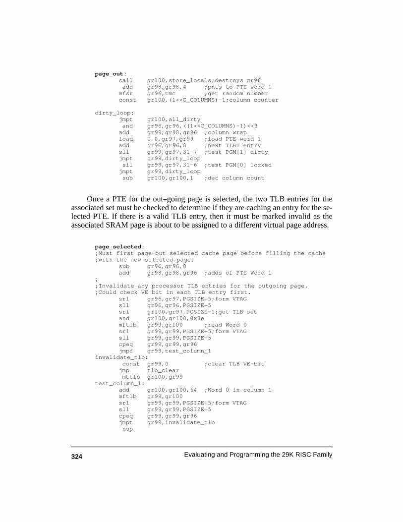
324 Evaluating and Programming the 29K RISC Family
page_out:call gr100,store_locals;destroys gr96 add gr98,gr98,4 ;pnts to PTE word 1mfsr gr96,tmc ;get random numberconst gr100,(1<<C_COLUMNS)–1;column counter
dirty_loop:jmpt gr100,all_dirty and gr96,gr96,((1<<C_COLUMNS)–1)<<3add gr99,gr98,gr96 ;column wrapload 0,0,gr97,gr99 ;load PTE word 1add gr96,gr96,8 ;next TLBT entrysll gr99,gr97,31–7 ;test PGM[1] dirtyjmpt gr99,dirty_loop sll gr99,gr97,31–6 ;test PGM[0] lockedjmpt gr99,dirty_loop sub gr100,gr100,1 ;dec column count
Once a PTE for the out–going page is selected, the two TLB entries for theassociated set must be checked to determine if they are caching an entry for the se-lected PTE. If there is a valid TLB entry, then it must be marked invalid as theassociated SRAM page is about to be assigned to a different virtual page address.
page_selected:;Must first page–out selected cache page before filling the cache;with the new selected page.
sub gr96,gr96,8add gr98,gr98,gr96 ;adds of PTE Word 1
;;Invalidate any processor TLB entries for the outgoing page.;Could check VE bit in each TLB entry first.
srl gr96,gr97,PGSIZE+5;form VTAGsll gr96,gr96,PGSIZE+5srl gr100,gr97,PGSIZE–1;get TLB setand gr100,gr100,0x3emftlb gr99,gr100 ;read Word 0srl gr99,gr99,PGSIZE+5;form VTAGsll gr99,gr99,PGSIZE+5cpeq gr99,gr99,gr96jmpf gr99,test_column_1
invalidate_tlb: const gr99,0 ;clear TLB VE–bit jmp tlb_clear mttlb gr100,gr99
test_column_1:add gr100,gr100,64 ;Word 0 in column 1mftlb gr99,gr100srl gr99,gr99,PGSIZE+5;form VTAGsll gr99,gr99,PGSIZE+5cpeq gr99,gr99,gr96jmpt gr99,invalidate_tlb nop
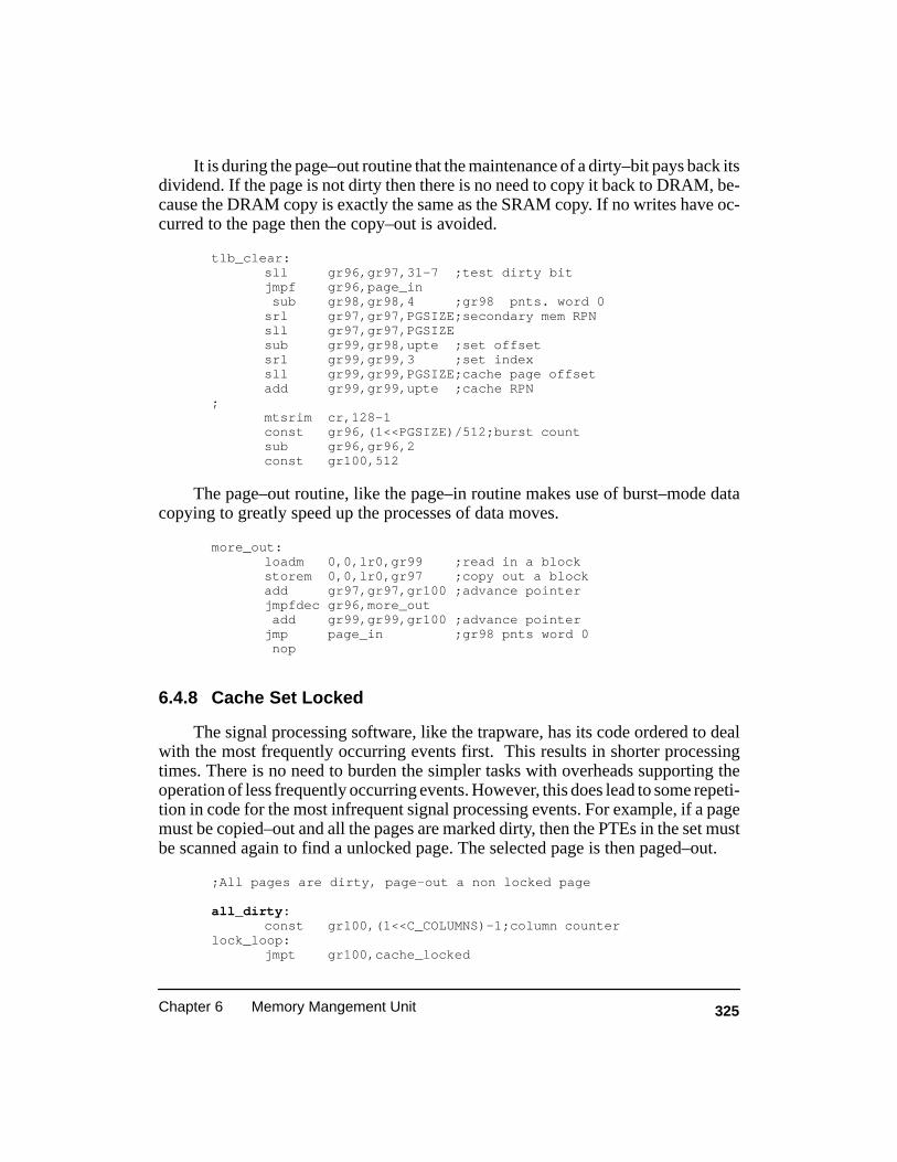
325Chapter 6 Memory Mangement Unit
It is during the page–out routine that the maintenance of a dirty–bit pays back itsdividend. If the page is not dirty then there is no need to copy it back to DRAM, be-cause the DRAM copy is exactly the same as the SRAM copy. If no writes have oc-curred to the page then the copy–out is avoided.
tlb_clear:sll gr96,gr97,31–7 ;test dirty bitjmpf gr96,page_in sub gr98,gr98,4 ;gr98 pnts. word 0srl gr97,gr97,PGSIZE;secondary mem RPNsll gr97,gr97,PGSIZEsub gr99,gr98,upte ;set offsetsrl gr99,gr99,3 ;set indexsll gr99,gr99,PGSIZE;cache page offsetadd gr99,gr99,upte ;cache RPN
;mtsrim cr,128–1const gr96,(1<<PGSIZE)/512;burst countsub gr96,gr96,2const gr100,512
The page–out routine, like the page–in routine makes use of burst–mode datacopying to greatly speed up the processes of data moves.
more_out:loadm 0,0,lr0,gr99 ;read in a blockstorem 0,0,lr0,gr97 ;copy out a blockadd gr97,gr97,gr100 ;advance pointerjmpfdec gr96,more_out add gr99,gr99,gr100 ;advance pointerjmp page_in ;gr98 pnts word 0 nop
6.4.8 Cache Set Locked
The signal processing software, like the trapware, has its code ordered to dealwith the most frequently occurring events first. This results in shorter processingtimes. There is no need to burden the simpler tasks with overheads supporting theoperation of less frequently occurring events. However, this does lead to some repeti-tion in code for the most infrequent signal processing events. For example, if a pagemust be copied–out and all the pages are marked dirty, then the PTEs in the set mustbe scanned again to find a unlocked page. The selected page is then paged–out.
;All pages are dirty, page–out a non locked page
all_dirty:const gr100,(1<<C_COLUMNS)–1;column counter
lock_loop:jmpt gr100,cache_locked

326 Evaluating and Programming the 29K RISC Family
and gr96,gr96,((1<<C_COLUMNS)–1)<<3add gr99,gr98,gr96 ;column wrapload 0,0,gr97,gr99 ;load word 1add gr96,gr96,8 ;next PTE entrysll gr99,gr97,31–6 ;test PGM[0] lockjmpt gr99,lock_loop sub gr100,gr100,1 ;dec column count
;jmp page_selected: nop
If all pages associated with the current set are marked locked, then the signalhandler arranges to have the DRAM page mapped directly to the faulting virtual ad-dress. This reduces the access times for all data and instructions contained in thepage. The algorithm does not try and restore the page to SRAM at a later date
;All columns for the current set are locked.;Map the virtual address to non–cache secondary memory.
cache_locked:srl gr96,tav,PGSIZE+5;form VTAGsll gr96,gr96,PGSIZE+5mfsr gr97,mmu ;get TIDand gr97,gr97,0xffor gr96,gr96,gr97 ;or in TIDconst gr97,0x4700 ;VE|UR|UW|UEor gr97,gr96,gr97 ;or in permissionsmfsr gr98,lrumttlb gr98,gr97 ;assign Word 0
;add gr98,gr98,1srl gr96,tav,PGSIZE ;form RPNsll gr96,gr96,PGSIZEmttlb gr98,gr96 ;assign Word 1
6.4.9 Returning from Signal Handler
When the signal handler has completed its processing, the context of the proces-sor at the time of the original TLB trap must be restored and execution continued.First, the user’s global registers, temporarily made use of by the operating system,must be restored from the Supervisor memory stack. Interrupts must be disabled andthe processor state frozen while the special support registers are restored from thesignal frame. Once this has been accomplished and the memory stack is restored to itspre–trap value, an IRET instruction is used to restart the instruction in execute at thetime the translation trap was taken.
;Pop registers of supervisor mode stack and;return to program causing the TLB miss.
ret_user:

327Chapter 6 Memory Mangement Unit
pop gr100,kmsppop gr99,kmsppop gr98,kmsppop gr97,kmsppop gr96,kmsp
;mtsrim cps,0x73 ;disable interruptspop tav,kmsp ;restore tavmtsrim cps,0x473 ;turn on FREEZEpopsr ops,it0,kmsppopsr alu,it0,kmsppopsr chc,it0,kmsppopsr chd,it0,kmsppopsr cha,it0,kmsppopsr pc2,it0,kmsppopsr pc1,it0,kmsppopsr pc0,it0,kmsppop rab,kmsp ;pop rabpop it1,kmsp ;pop rspadd gr1,it1,0 ;alu operationadd kmsp,kmsp,4 ;discount signaliret
6.4.10 Support Routines
The example code used two support routines to copy the 128 32–bit local regis-ters to and from the Supervisor memory stack. Most operating systems assign all ofthe local registers for use by the user’s application code. The large number of regis-ters effectively implements a data cache. The advantage to having several registers isthat, unlike data memory, the register file supports simultaneous read and write ac-cess. In order to support maximum length data bursts on page transfers, the registerfile is made available to the signal processing routine.
;Push local registers onto Supervisor M–stack
store_locals:const gr96,512 ;Window Sizesub kmsp,kmsp,gr96mtsrim cr,128–1 ;save 128 registersjmpi gr100 ;return storem 0,0,lr0,kmsp
;Pop local registers off Supervisor M–stack
load_locals:const gr96,512 ;Window Sizemtsrim cr,128–1 ;load 128 registersloadm 0,0,lr0,kmspjmpi gr100 ;return add kmsp,kmsp,gr96
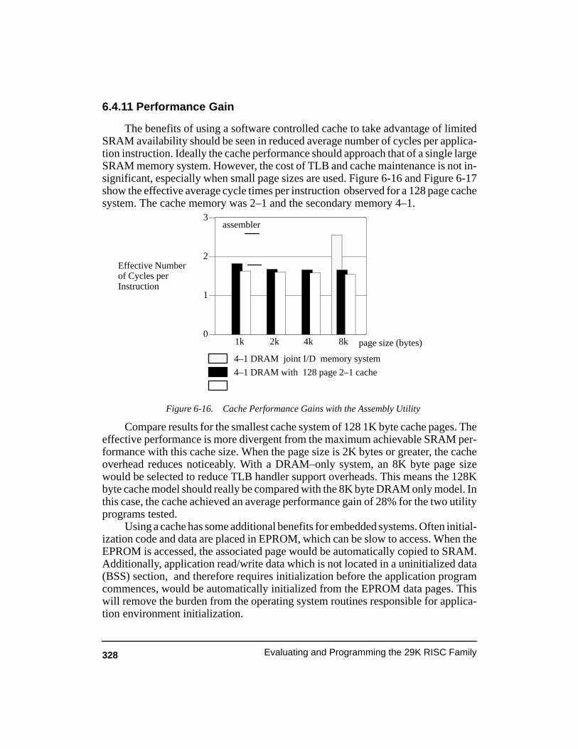
328 Evaluating and Programming the 29K RISC Family
6.4.11 Performance Gain
The benefits of using a software controlled cache to take advantage of limitedSRAM availability should be seen in reduced average number of cycles per applica-tion instruction. Ideally the cache performance should approach that of a single largeSRAM memory system. However, the cost of TLB and cache maintenance is not in-significant, especially when small page sizes are used. Figure 6-16 and Figure 6-17show the effective average cycle times per instruction observed for a 128 page cachesystem. The cache memory was 2–1 and the secondary memory 4–1.
0
1
2
3
1k 2k 4k 8k
4–1 DRAM with 128 page 2–1 cache
4–1 DRAM joint I/D memory system
assembler
page size (bytes)
Figure 6-16. Cache Performance Gains with the Assembly Utility
Effective Numberof Cycles perInstruction
Compare results for the smallest cache system of 128 1K byte cache pages. Theeffective performance is more divergent from the maximum achievable SRAM per-formance with this cache size. When the page size is 2K bytes or greater, the cacheoverhead reduces noticeably. With a DRAM–only system, an 8K byte page sizewould be selected to reduce TLB handler support overheads. This means the 128Kbyte cache model should really be compared with the 8K byte DRAM only model. Inthis case, the cache achieved an average performance gain of 28% for the two utilityprograms tested.
Using a cache has some additional benefits for embedded systems. Often initial-ization code and data are placed in EPROM, which can be slow to access. When theEPROM is accessed, the associated page would be automatically copied to SRAM.Additionally, application read/write data which is not located in a uninitialized data(BSS) section, and therefore requires initialization before the application programcommences, would be automatically initialized from the EPROM data pages. Thiswill remove the burden from the operating system routines responsible for applica-tion environment initialization.
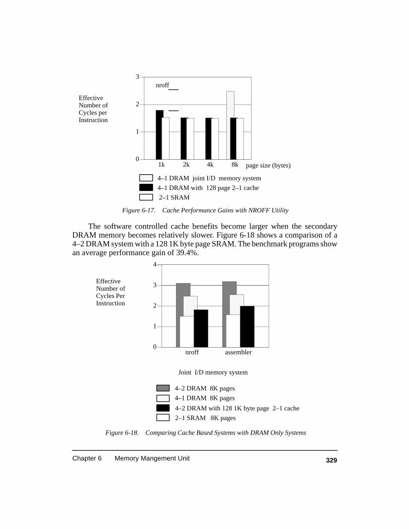
329Chapter 6 Memory Mangement Unit
0
1
2
3
1k 2k 4k 8k
4–1 DRAM with 128 page 2–1 cache
2–1 SRAM
4–1 DRAM joint I/D memory system
nroff
page size (bytes)
Figure 6-17. Cache Performance Gains with NROFF Utility
EffectiveNumber ofCycles perInstruction
The software controlled cache benefits become larger when the secondaryDRAM memory becomes relatively slower. Figure 6-18 shows a comparison of a4–2 DRAM system with a 128 1K byte page SRAM. The benchmark programs showan average performance gain of 39.4%.
0
1
2
3
4
nroff assembler
4–1 DRAM 8K pages
4–2 DRAM with 128 1K byte page 2–1 cache
4–2 DRAM 8K pages
2–1 SRAM 8K pages
Joint I/D memory system
Figure 6-18. Comparing Cache Based Systems with DRAM Only Systems
EffectiveNumber ofCycles PerInstruction

330 Evaluating and Programming the 29K RISC Family
October 13 1995, Draft 1
331
Chapter 7
Software Debugging
This chapter supports software engineers wishing to develop application codeor operating system code for execution on a 29K RISC microprocessor.
Debugging tools which can be used in both a hardware and software debuggingrole, such as in–circuit emulators and logic analyzers, are not described; that is left tothe individual tool manufacturer. The material presented concentrates on describingthe operation of inexpensive tools based on the MiniMON29K debug monitor andUniversal Debug Interface (UDI). Figure 7-1 shows the various tools used duringthe different stages of an embedded processor–based project. Debug monitors aretypically used during the initial processor evaluation and selection stage, and laterwhen software is debugged with a working hardware system.
Also described are processor features which were specifically included in thedesign for the purpose of debugging. The precise details of how these features areconfigured to build a debug monitor such as MiniMON29K will not be described indetail. This chapter is not intended to show how debug tools are constructed, but rath-er to show how existing tools can be utilized and describe their inherent limitations.However, readers wishing to build their own tools will be able to glean the informa-tion required.
7.1 REGISTER ASSIGNMENT CONVENTION
The 29K processor calling convention divides the processor registers into twogroups: those available to the run–time application, and hence used by compiler gen-erated code, and those reserved for operating system use.
All the 29K processor’s 128 local registers, used to implement the register stackcache, are allocated to application code use. In addition, 32 (gr96–gr127) of the 64

October 13 1995, Draft 1
332 Addendum to –– Evaluating and Programming the 29K RISC Family
Packaged Benchmarks
AMD Literature
Compiler Tool Chain
Architectural Simulator
Start system design
Evaluation Board
LogicAnalyserWaveform
Simulator
Hard Work +Careful Analysis
Compiler Tool Chain
EvaluationBoard
ICE
LogicAnalyzer
Homework +Scope + Time
DebugedMemorySystem
Initial h/w withoutworking memory
system
Application Benchmarks
MiniMON29KJTAGEmulator
ICE Analyser +Disasemmbler
Initial s/w
Working h/w + s/w
s/w path h/w path
ASIC
Processor Selection
ROMEmulator
s/w running on h/w
Instruction SetSimulator
S/w and h/wDevelopment
S/w and h/wIntegration
Figure 7-1. 29K Development and Debug Tools

October 13 1995, Draft 1
333Chapter 7 Software Debugging
global registers are assigned to application use, and the remaining group of 32(gr64–gr95) are for operating system use.
The processor does not assign any particular task to the global registers in theoperating system group. However, over time a convention has evolved among 29Kprocessor users. The subdivision of global registers gr64–gr95 into sub groups wasdescribed in section 3.3, and is widely adhered to; the methods presented in this chap-ter shall continue with the convention.
The subgroups are known as: The interrupt Freeze mode temporaries (givensynonyms it0–it3); the operating system temporaries (kt0–kt11); and the operatingsystem static support registers (ks0–ks15).
7.2 PROCESSOR DEBUG SUPPORT
7.2.1 Execution Mode
The processor is in Supervisor mode whenever the SM–bit in the Current pro-cessor Status register (CPS) is 1. If the SM bit is 0, the processor is executing in Usermode. When operating in User mode the processor cannot access protected re-sources or execute privileged instructions.
Generally a processor maintains context information which refers to operatingsystem status and various user processes. Operating in User mode is a means of pre-venting a User mode process from accessing information which belongs to anothertask or information that the operating system wishes to keep hidden.
If a User mode task breaks any of the privilege rules described in the processor’sUser Manual, then a protection violation trap is taken. Traps cause the operating sys-tem to regain control of execution. Typically the operating system will then send asoftware signal to the User mode process reporting its violation and possibly stop-ping its execution. The exact action which takes place is particular to each operatingsystem implementation.
Besides preventing User mode programs from using processor instructionswhich are reserved for operating use only, an operating system can precisely control aprocesses access to memory and registers. This can be very useful when debuggingUser mode software. The following section describes the processor’s memory man-agement support. The register protection scheme is very simple. Special registerRBP is used to restrict banks of global registers to Supervisor mode access only. Eachbank consists of 16 registers and a 1 in each RBP bit position restricts the correspond-ing bank to Supervisor mode access only. Thus, it is normal to set RBP=0x3F, whichallows User mode processes to access global registers gr96 and higher. These are theonly registers which can be affected by compiler generated code. Note however,global registers gr0 and gr1 which perform special support tasks are effected by com-piler generated code and their access is not restricted by the RBP protection scheme.

October 13 1995, Draft 1
334 Addendum to –– Evaluating and Programming the 29K RISC Family
7.2.2 Memory Access Protection
A number of the 29K processor family members are equipped with a Transla-tion Look–aside buffer (TLB). It is intended for construction of a Memory Manage-ment Unit (MMU) scheme. A complete description of the TLB operation is given inMemory Management Unit (Chapter 6).
An MMU is normally used to provide virtual memory support. However, it canalso play an important debugging role, even in embedded applications. Note, thisfunction is not intended to be performed by the Region Mapping facility provided onsome family members. The Region Mapping facility does not support the addressspace granularity supported by the TLB hardware. In addition, Region Mapping insome cases only allows address mapping to a limited region of physical memory. Forexample, on the Am29200 microcontroller, only the DRAM memory and not theROM memory can be accessed in virtual address space.
When code is being developed, often an erroneous data reference will occur. Ifno memory is located at the particular address then the target memory system shouldgenerate a hardware access error (such as DERR or IERR on some family members).However, address aliasing often results in the access being performed on some otheraddress location for which address decoding determines physical memory has beenassigned. This kind of programming bug can be difficult to detect. Using the TLB,address access errors can be immediately detected and reported to the operating sys-tems via access protection violations.
The OS–boot operating system, used by many customers, can provide memoryaccess protection by mapping virtual address to physical addresses in a one–to–oneformat. This is adequate for many embedded applications where memory pagingdoes not occur and application programs can be completely located in availablememory. When an access violation occurs OS–boot informs the MiniMON29Kmonitor who reports the violation to the process controlling debugging. The detailsof this mechanism are described in later sections.
Whether you intend using OS–boot or some other operating system, it is likelyyou would benefit from using the on–chip TLB hardware to support a more powerfuldebug environment, via the detection of invalid memory references.
7.2.3 Trace Facility
Using the Trace Facility, a program can be executed one instruction at a time.This allows the execution of a program to be followed and the state of the processorto be examined and modified after each instruction has executed.
The 29K family has a four stage pipeline: Fetch, Decode, Execute and Write–back. Tracing is enabled by setting the Trace enable (TE) bit in the CPS register.When an instruction passes from the execute stage of the pipeline into the write–backstage, the TE bit is copied into the TP bit. The Trap Pending (TP) bit is also located inthe CPS register, and when it becomes set the processor takes a trace trap. The Super-

October 13 1995, Draft 1
335Chapter 7 Software Debugging
visor mode code normally arranges for the vector table entry for the trace trap tocause the debug monitor to gain control of the processor.
The debug monitor, normally MiniMON29K, uses the IRET instruction to re-start program execution after the Trace trap handler has completed. Execution of anIRET causes the Old Processor Status register (OPS) to be copied into the CPS regis-ter before the next program instruction is executed. The TP bit in the OPS is normallycleared by the debug monitor before the IRET is executed. If the TE bit in the OPS isset then tracing of the restarted instruction sequence shall continue after executingthe IRET.
Note, when the disable all (DA) bit in the CPS register is set the trace trap cannotbe taken unless the processor supports Monitor mode (described below). Should theprogram being debugged issue an instruction such as ASNEQ, it will then take a trapand the DA bit will become set. The OPS and CPS registers will have the TP bit setbut a trace trap will not be taken. This means that Freeze mode code (trap handlerswhich execute with the DA bit set) cannot be debugged by a software debug monitorunless the processor supports Monitor mode. Most members of the 29K processorfamily do not support Monitor mode.
7.2.4 Program Counter register PC2
The instruction following a branch instruction, known as the delay instruction,is executed regardless of the outcome of the branch. This performance improvingtechnique requires that two registers be used to record the addresses of the instruc-tions currently in the execute and decode stages of the processor pipeline. When abranch is taken the PC0 register contains the address of the target instruction as it en-ters the decode stage of the pipeline. Register PC1 always contains the address of theinstruction in execute. When the target instruction of a branch enters decode theinstruction in execute is the delay slot instruction following the branch.
Program counter registers PC0 and PC1 are required to restart the processorpipe–line in the event of a trap or an interrupt occurring. Many of the synchronoustraps, such as a register access privilege violation, cause execution to be stopped withthe address of instruction causing the violation held in PC1 (execute address).Asynchronous traps, such as an external interrupt, and instruction traps, such as AS-SERT instructions, cause the address of the instruction following the one in executeat the time of the interrupt to be held in the PC1 register. In fact when a trap or inter-rupt is taken the PC register values are frozen and used to restart program executionlater. The frozen PC values are held in a 3 register PC–buffer. Of course, the actual PCregisters continue to be used. Instructions such as MTSR and MFSR (move–to andmove–from special register) can be used to modify the PC–buffer register values.
The address of the instruction previously in execute and now in write–back isheld in the PC2 register. This is very convenient because a debugger can determinethe instruction which was in execute at the time the interrupt or trap occurred. The
October 13 1995, Draft 1
336 Addendum to –– Evaluating and Programming the 29K RISC Family
trace trap is an asynchronous trap, and thus after the trap is taken the next instructionabout to execute is addressed by PC1. Some family members support InstructionBreakpoint registers, which can be used to stop execution when a certain addressreaches execute. When this occurs a synchronous trap is taken and the instruction isstopped before execution is completed.
Debug monitors, such as MiniMON29K, understand the operation of the PCregisters and can use them to control program execution. When MiniMON29K isused with a processor which has no Breakpoint registers, a technique relying on tem-porarily replacing instructions with illegal opcode instructions is used to implementbreakpoints. Illegal opcode instructions are used in preference to trap instructions be-cause execution is stopped with the PC–buffer recording execution a cycle earlier.That is, the breakpoint address is in PC1 rather than PC2, as would happen with a trapinstruction.
One further useful feature of the PC2 register occurs when breakpoints are set tothe first instruction of a new instruction sequence — typically the first instruction of aprocedure. When the breakpoint is taken and program execution is stopped, the PC2register contains the address of the delay slot instruction executed before the newinstruction sequence started. This is very useful in determining where a program waspreviously executing.
7.2.5 Monitor Mode
Monitor Mode currently only applies to a limited numbr of 29K processors, seeTable 7-1. If a trap occurs when the DA bit in the CPS register is a 1, the processorstarts executing at address 16 in instruction ROM space. Monitor Mode is not enteredas a result of asynchronous events such as timer interrupts or activation of theTRAP(1–0) or INTR(3–0) lines.
On taking a Monitor Mode trap the Reason Vector register (RSN) is set by theprocessor to indicate the cause of the trap. Additionally, the MM bit in the CPS regis-ter is set to 1. When the MM bit is set, the shadow program counters (SPC0, SPC1,and SPC2) are frozen, in a similar way to the FZ bit freezing the PC0–PC2 bufferregisters. Because the shadow program counters continue to record PC-BUS activitywhen the FZ bit is set, they can be used to restart Freeze Mode execution. This isachieved by an IRET or IRETINV instruction being executed while in MonitorMode.
Monitor mode traps are used by monitors in the debugging of trap and interrupthandlers and are not intended for operating system use.
7.2.6 Instruction Breakpoints
Some members of the 29K processor family support Instruction Breakpoint reg-isters, see Table 7-1. These registers can be used to stop a program’s execution when

October 13 1995, Draft 1
337Chapter 7 Software Debugging
Table 7-1. 29K Family On–chip Debug Support
Processor virtualmemory
yesno –
instructionbreakpoints
Am29000
Monitor mode databreakpoints
– –
data breakpointsvalue ranges
yesno –Am2903x – –
yesno 2Am29040 1 no
yesyes 2Am29050 – –
nono –Am2920x – –
yesno –Am2924x – –
yesyes 2Am29460 1 yes
nono –Am29005 – –
an instruction at a specified address enters execute. The control mechanism forBreakpoints is flexible, allowing a User process ID to be specified.
With 3–bus processors, breakpoints can be assigned to Instruction space orROM space. Both of these spaces normally contain instructions but the ROM spacetypically contains ROM rather than RAM memory devices. No matter which kind ofmemory device is utilized the Breakpoint registers can be used.
When a processor does not support Breakpoint registers, illegal instructions ortraps are used to stop execution at desired address locations. Debug monitors are,however, unable to manipulate instructions which are located in ROM devices. Thusthe main uses of the Breakpoint register is to support breakpoints when ROM devicesare in use. Additionally, they are used in the rare case where a 3–bus Harvard archi-tecture memory system is constructed without providing a means for the processor toread and write instruction space. In this case the processor will not be able to replaceinstructions at a breakpoint addresses with temporary illegal instructions.
The MiniMON29K debug monitor, described in detail later, must make somedecision about the values to put in the breakpoint register fields: BTE (break ontranslation enable) and BPID. The debug tool user (Debugger Front End user) nor-mally selects the process identifier (PID) of the application process containing thebreakpoint. However, the DFE often does not know if the 29K operating system isrunning with address translation turned on. The DebugCore accesses a data structureshared with the operating system to determine the value for the BTE field, see sectionD.3.4. The operating system is required to fill in the appropriate sections of the shareddata structure, informing the DebugCore of the CPS register value to be used duringprogram execution. When the PI (physical instruction) bit in the CPS register is clearthe BTE bit is set.

October 13 1995, Draft 1
338 Addendum to –– Evaluating and Programming the 29K RISC Family
7.2.7 Data Breakpoints
Currently only the Am29040 processor supports Data Breakpoint registers, seeTable 7-1. These registers can be used to stop a program’s execution when data is ei-ther read or written from an address which lies within a specified range. The controlmechanism is flexible and shares much of the characteristics provided by the Instruc-tion Breakpoints Control registers described in the previous section.
When an address match is detected, a trace trap is taken after the load or storeinstruction is completed (this is also true for loadm and storem instructions). When atrap is taken, the PC1 registers points to the instruction following the load or store andthe data transfer has occurred.
To make effective use of data breakpoints it is important that the selected debug-ger has support for controlling the operation of the on–chip support registers. DataBreakpoint Control registers are a relatively new feature and many debuggers havenot yet been extended to incorporate the necessary command and control functions.
7.3 THE MiniMON29K DEBUGGER
Developers of software for embedded applications are used to working withemulators. They enable code to be down–loaded to application memory or installedin substitute overlay memory. This avoids having the development delays associatedwith running code from EPROM. The use of emulators may be a necessary stage infirst getting the target hardware functional; for this task their ability to work with par-tially functioning hardware makes them indispensable. However, once the processoris able to execute out of target system memory and a communications channel such as
Figure 7-2. MinMON29k Debugger Components
MonDFEDebug processrunning on DFEhost processor
MonTIPTarget–interfaceProcess on TIPhost processor
29K RISC processor andapplication–specific hardware,with MiniMON29K DebugCoreand OS–boot in ROM memory
Application downloaded fromMonDFE into RAM memory
UDIlink
private link

October 13 1995, Draft 1
339Chapter 7 Software Debugging
a serial link is available, the need for an emulator is reduced. Emulators are expen-sive, and it is not always possible to make one available to each team member. Theuse of a debug monitor such as the MiniMON29K monitor during the software debugstage of a project is an economical alternative to an emulator.
The MiniMON29K monitor is not intended to be a standalone monitor. That is,it requires the support of a software module known as the Target Interface Process(TIP). The TIP executes on a separate host processor. The embedded 29K target pro-cessor communicates with the TIP via a serial link or other higher performance chan-nel (see Figure 7-2). The User–Interface process, known as the Debugger Front End(DFE), communicates with the TIP via the inter–process communication mechanismknown as UDI which is described later.
Most monitors do not offer high level language support. Assembly code instruc-tions must be debugged rather than the original, say C, code. Using GDB in conjunc-tion with the MiniMON29K monitor enables source level code to be debugged,which is far more productive and necessary for large software projects. (More on thisin the UDI section).
MiniMON29K has a small memory requirement, for both instruction memoryand data memory of the target 29K system. The size is reduced by implementingmuch of the support code in the TIP host machine, and communicating with the targetvia high–level messages. The amount of communication required is reduced by in-corporating sophisticated control mechanisms in the target DebugCore.
Much of the following discussion in this section, is concerned with describingthe operating principles of target hardware software components. Other Mini-MON29K components such as MonTIP and MonDFE are described in the later UDIsections.
7.3.1 The Target MiniMON29K Component
The embedded portion of the MiniMON29K monitor must be installed in targetsystem ROM or down–loaded by the host via a shared memory interface. The targetapplication code and additional operating system code can then be down–loaded viathe message system. If changes to the code are required, then the message system canbe used to quickly down–load new code without changing any ROM devices.
The software installed in the target hardware consists of a number of modules,described in Figure 7-3. When the embedded Am29000 processor is reset, the initialoperating system module, OS, takes control. This module initializes the processorand the other support modules. The monitor components are required to implement amessage communications driver and a debug control core (DebugCore).
The operating system module is not part of the MiniMON29K monitor. This al-lows developers to build their own operating system or make use of a 3rd–party real–time executive product. However, AMD does supply processor initialization codeand HIF system call support routines. HIF is an embedded system call interface spec-

October 13 1995, Draft 1
340 Addendum to –– Evaluating and Programming the 29K RISC Family
Figure 7-3. 29K Target Software Module Configuration
message systemMSG
MiniMON29KDebugCcore 2.0
DBG
DebugCoreconfiguration
CFG
communica-tion drivers
OS–boot
HIF
Application
SER
MiniMON29K
initialization
floating–pointtrapware
run–timesupport
memorymanagement
OS Monitor
link toMonTIP
ification, which many of the 29K processor support library services make use of. TheAMD supplied operating system code is known as OS–boot, and it is normally sup-plied in the same ROM containing the MiniMON29K target component software.(All of the OS–boot and MiniMON29K 29K source code is freely available fromAMD).
7.3.2 Register Usage
The DebugCore, message driver and other MiniMON29K monitor modules donot require any processor registers to be reserved for their use. This means that all theprocessor registers are available for use by the operating system and applicationcode.
What this really means is that any registers temporarily used by MiniMON29Kcode are always restored. The only exception to this occurs with global register gr4and the TE and TP bits of the CPS special register.
Global register gr4 is implemented in some members of the 29K family but notreported in the relevant User Manual, as it is never used by application or operatingsystem code. With family members which have no gr4 register, the ALU forwardinglogic can be used to keep a temporary register alive for 1 processor cycle following itsmodification. The gr4 data is lost during the write–back stage when there is no realgr4 register in the global register file. Note, software such as the MiniMON29K De-bugCore can be difficult to debug because emulators also make use of gr4 in analyz-ing processor registers.

October 13 1995, Draft 1
341Chapter 7 Software Debugging
The TE and TP bits, located in the Current Processor Status register, belong tothe MiniMON29K DebugCore. However, the CPS register really belongs to the op-erating system and the OS should not modify the TE and TP bits which are main-tained by the DebugCore. When the operating system issues an IRET instruction itupdates the CPS register with the contents of the OPS register. Normally the Debug-Core will set the TE bit in the OPS before the operating system performs an IRET.However, initially the operating system must call the support routine dbg_iret() toperform the IRET on behalf of the operating system. This gives the DebugCore anopportunity to gain control of the TE bit.
7.3.3 The DebugCore
The TIP host processor controlling the target 29K processor sends messages viathe available link to the DebugCore module. The message system enables the host toexamine and change registers and memory in the target hardware. Program execu-tion can also be controlled via instruction breakpoints and single stepping instruc-tions. Messages are provided specifically for controlling processor execution.
The DebugCore decodes the messages, giving access to the 29K processor reg-isters and the target system memory. However, it does not access the non–processorresources directly. The Configuration Control Module supports the peek and pokefunctions shown below. These functions are used for all non–register space targethardware access. Note, all functions and data variables defined in the configurationMiniMON29K module begin with the cfg_ prefix.
void cfg_peek(to, from, count, space, size)
void cfg_poke(to, from, count, space, size)
The peek function is used to read from target space into temporary debug coreBSS memory space. The poke function is used when writing to target space. The‘space’ parameter is used to indicate the target address space, according to the re-ceived message parameters. Typical space field values would enable instructionspace, data space or I/O space access. The ‘size’ field is used to indicate the size, inbytes, of the objects being transferred. The CFG module normally tries to makememory accesses in the size indicated. However, if a memory system does not sup-port, say, byte–write access to ROM–space, then the CFG access functions can beconfigured to perform byte manipulation via word–sized memory accesses. By keep-ing the access functions separate, a user can configure the peek and poke functionsfor any special requirements without having to understand the DebugCore module.Peek and poke functions are supplied for typical existing target hardware.
For example, if a system uses Flash memory devices, the erase and program-ming sequences required to write to Flash should be built into the cfg_poke() proce-

October 13 1995, Draft 1
342 Addendum to –– Evaluating and Programming the 29K RISC Family
dure. If Flash and other device types, such as DRAM, are used in the same memoryspace, then the cfg_poke() procedure can examine the address value in the ‘to’ pa-rameter to determine the correct operation. Recent versions of MiniMON29K haveincluded CFG module support for Flash memory devices.
When the target processor stops executing operating system or applicationcode, a context switch occurs into the DebugCore context. The state of the processoris recorded when switching context, thus enabling execution to be resumed withoutany apparent interruption. The DebugCore context may be entered for a number ofreasons, such as: a message was received from the TIP host, an instruction breakpointwas encountered, a memory access violation occurred. Whenever the DebugCoregains control a ‘halt’ message is sent to the TIP host processor. The TIP host and tar-get can then exchange messages as necessary to analyse or change the state of theprocessor or memory.
DebugCore 2.0 shares a data structure with the operating system (OS). Vectortable entry 71 is initializes by the OS to point to the data structure. Appendix D de-scribes the DebugCore and OS interface in detail. The data structure is mainly used topass the address of entry points within the two software modules. Address labels canbe determined at link time. However, when, say, a new OS is loaded at run time itmust reconnect with the DebugCore. This requires address labels be available at runtime. In addition to address labels are various fields which support the DebugCoreinstalling per process breakpoints and requesting OS supplied service functions.
7.3.4 DebugCore installation
It is very simple to install the DebugCore with any operating system. Mainly,what is required is use of a number of Vector Table entries which are not normallyrequired for operating system operation. And to call the DebugCore initializationroutine dbg_control(). Figure 7-4 shows the vector table entries required. The twomost obvious entries are for trap number 0 (illegal opcode) and number 15 (trace

October 13 1995, Draft 1
343Chapter 7 Software Debugging
trap). These table entries point to the DebugCore entry labels dbg_V_bkpt anddbg_V_trace, respectively. Note, all the DBG module functions and data structurenames begin with the dbg_ prefix.OS Cold–Start
The operating system is responsible for inserting the necessary address labelsinto the vector table. Any vector table entries which are not required by the operatingsystem can be defaulted to the DebugCore, via the dbg_trap entry. When this entry isused, register gr64 should contain the original trap number (see section D.4.1 for al-ternatives). It can be very useful to direct traps such as protection violation (number5) and Data TLB protection Violation (number 13) into the DebugCore. This is muchbetter than just issuing a HALT instruction in the operating system. When a trap istaken into the DebugCore a message is sent to the MonTIP process which will informthe DFE process when execution has halted. DFEs such as MonDFE and GDB under-stand the 29K trap number assignment and can report a trap number 13 as a Usermode data protection violation (Segmentation fault in Unix language).
Initializing the vector table is part of what is known as the operating systemcold–start code. The operating system start–up sequence is shown in Figure 7-5.
When the processor’s power is applied, or when the *RESET pin is asserted, theCPU begins executing instructions at location 0 in ROM instruction space (ROMspace and instruction space are the same in many 29K family members). Control isusually passed directly to the operating system cold–start code. To save the contentsof all the processor’s registers before the system is initialized, the user may modify
V_BKPT
Figure 7-4. Vector Table Assignment for DebugCore 2.0
dbg_V_bkptVAB
V_TRACE
V_INTR0
V_DBG_MSG
V_OS_MSG
V_RESET
75
76
255
V_PROT5
15
example 16
0
dbg_trap,gr64=5
dbg_V_trace
msg_intr
virtual interrupts, 75
and 76
dbg_V_msg
os_V_msg
71OS/DebugCoreshared data structure
V_71
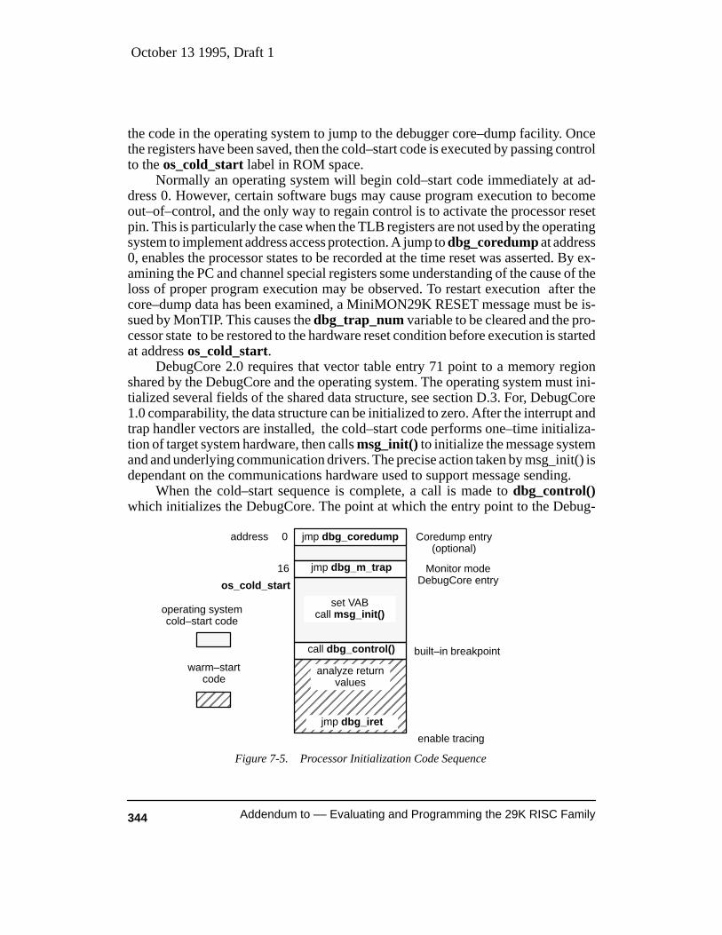
October 13 1995, Draft 1
344 Addendum to –– Evaluating and Programming the 29K RISC Family
the code in the operating system to jump to the debugger core–dump facility. Oncethe registers have been saved, then the cold–start code is executed by passing controlto the os_cold_start label in ROM space.
Normally an operating system will begin cold–start code immediately at ad-dress 0. However, certain software bugs may cause program execution to becomeout–of–control, and the only way to regain control is to activate the processor resetpin. This is particularly the case when the TLB registers are not used by the operatingsystem to implement address access protection. A jump to dbg_coredump at address0, enables the processor states to be recorded at the time reset was asserted. By ex-amining the PC and channel special registers some understanding of the cause of theloss of proper program execution may be observed. To restart execution after thecore–dump data has been examined, a MiniMON29K RESET message must be is-sued by MonTIP. This causes the dbg_trap_num variable to be cleared and the pro-cessor state to be restored to the hardware reset condition before execution is startedat address os_cold_start.
DebugCore 2.0 requires that vector table entry 71 point to a memory regionshared by the DebugCore and the operating system. The operating system must ini-tialized several fields of the shared data structure, see section D.3. For, DebugCore1.0 comparability, the data structure can be initialized to zero. After the interrupt andtrap handler vectors are installed, the cold–start code performs one–time initializa-tion of target system hardware, then calls msg_init() to initialize the message systemand and underlying communication drivers. The precise action taken by msg_init() isdependant on the communications hardware used to support message sending.
When the cold–start sequence is complete, a call is made to dbg_control()which initializes the DebugCore. The point at which the entry point to the Debug-
Figure 7-5. Processor Initialization Code Sequence
0
jmp dbg_m_trap
set VABcall msg_init()
ÉÉÉÉÉÉÉÉÉÉÉÉÉÉÉÉÉÉÉÉÉÉÉÉÉÉÉÉÉÉÉÉÉÉÉ
call dbg_control()
jmp dbg_iret
analyze returnvalues
16
address
os_cold_start
built–in breakpoint
enable tracing
Coredump entry(optional)
Monitor modeDebugCore entry
operating systemcold–start code
ÉÉÉ
warm–startcode
jmp dbg_coredump
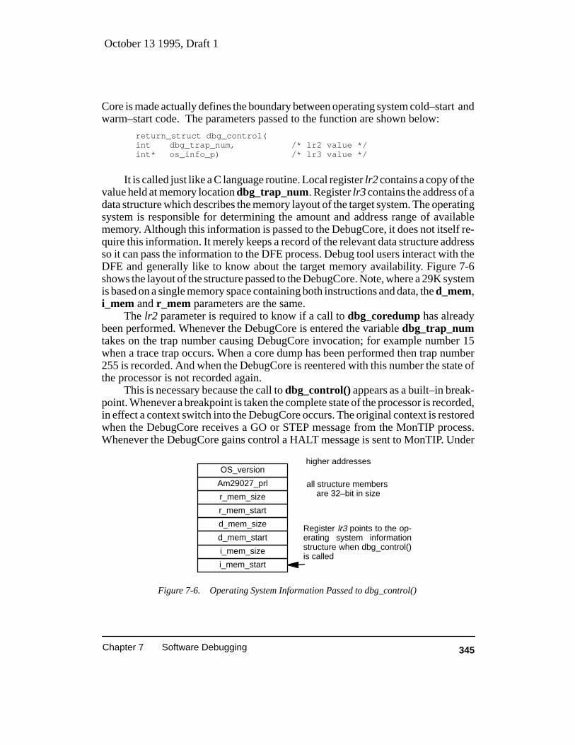
October 13 1995, Draft 1
345Chapter 7 Software Debugging
Core is made actually defines the boundary between operating system cold–start andwarm–start code. The parameters passed to the function are shown below:
return_struct dbg_control(int dbg_trap_num, /* lr2 value */int* os_info_p) /* lr3 value */
It is called just like a C language routine. Local register lr2 contains a copy of thevalue held at memory location dbg_trap_num. Register lr3 contains the address of adata structure which describes the memory layout of the target system. The operatingsystem is responsible for determining the amount and address range of availablememory. Although this information is passed to the DebugCore, it does not itself re-quire this information. It merely keeps a record of the relevant data structure addressso it can pass the information to the DFE process. Debug tool users interact with theDFE and generally like to know about the target memory availability. Figure 7-6shows the layout of the structure passed to the DebugCore. Note, where a 29K systemis based on a single memory space containing both instructions and data, the d_mem,i_mem and r_mem parameters are the same.
The lr2 parameter is required to know if a call to dbg_coredump has alreadybeen performed. Whenever the DebugCore is entered the variable dbg_trap_numtakes on the trap number causing DebugCore invocation; for example number 15when a trace trap occurs. When a core dump has been performed then trap number255 is recorded. And when the DebugCore is reentered with this number the state ofthe processor is not recorded again.
This is necessary because the call to dbg_control() appears as a built–in break-point. Whenever a breakpoint is taken the complete state of the processor is recorded,in effect a context switch into the DebugCore occurs. The original context is restoredwhen the DebugCore receives a GO or STEP message from the MonTIP process.Whenever the DebugCore gains control a HALT message is sent to MonTIP. Under
i_mem_start
i_mem_size
d_mem_start
d_mem_size
r_mem_start
r_mem_size
Am29027_prl
Figure 7-6. Operating System Information Passed to dbg_control()
Register lr3 points to the op-erating system informationstructure when dbg_control()is called
all structure members are 32–bit in size
OS_versionhigher addresses

October 13 1995, Draft 1
346 Addendum to –– Evaluating and Programming the 29K RISC Family
DFE direction, MonTIP can then send messages to the DebugCore to examine andchange the saved processor status.OS Warm–Start
The DebugCore records the return address for dbg_control() when it is firstcalled. The address is important because it is the start of the operating system warm–start code. When an application program is down–loaded to the target hardware, anINIT message is normally sent. The message contains information extracted from theapplication COFF file. This information along with other operating system run–timesupport data is passed to the operating system when the dbg_control() function re-turns. As is normal for C procedures, the return information is placed in global regis-ters starting with gr96. Figure 7-7 shows the format of the operating system warm–start data.
After the DFE (MonDFE for example) has been instructed to load a new pro-gram into memory, the return registers can be examined to verify their contents.Note, with some DFEs it is possible to load a COFF file without sending an INIT mes-sage. In this case the return registers are not affected and the PCs are not forced to thedbg_control() return address.
After loading a program a user will normally start execution, which causes theDebugCore to switch out of context and restore the context described in the registershadow memory. If an INIT message was received then execution will commence inthe operating system warm–start code. Otherwise, it continues from wherever the re-stored PC registers are located. Warm–start code normally examines the return struc-ture values and prepares the operating system run–time support accordingly. For ex-ample, register gr100 contains the start address of the down–loaded application pro-gram. The address value may be loaded in the PC–buffer registers before an IRETinstruction is used to start program execution. However, it is important to note that
register stack size
memory stack size
first instruction of User loaded code
end address of program data
start address of program data
end address of program text
start address of program text
Figure 7-7. Return Structure from dbg_control()
this register always 0
Operating system control info.
start of command line args (argv)
gr96
gr97
gr98
gr99
gr100
g101
gr102
gr103
gr104
gr105
October 13 1995, Draft 1
347Chapter 7 Software Debugging
the warm–start operation is entirely operating system dependent, and the code needpay no attention to the return structure information. The operation of OS–boot, nor-mally supplied along with MiniMON29K, is described in a later section.
7.3.5 Advanced DBG and CFG Module Features
Normally the call to dbg_control() implies that a built–in breakpoint should betaken. This gives the user an opportunity to down–load an application program be-fore execution is continued. However, by setting the call lr2 parameter to V_NOBRK(254), no breakpoint will be taken and the call will return with no need for a GO mes-sage from MonTIP. This enables the DebugCore to be initialized for operation, and isuseful where there is no requirement to download an application program. Of coursethere are no call return values for the operating system warm–start to examine. Thefacility enables the DebugCore to remain in a final system and only be called upon ina emergency such as memory access violation.
The CFG module is used to configure the operation of the DBG module. Thereis really no need to have the source code for the DBG module, only the CFG module.After configuring the CFG, it can be assembled and linked with the .o debug coremodules (dbg_core.o and dbg.o). The CFG supplies the cfg_peek() and cfg_poke() functions, as well as defining the number of breakpoints supported and the size of theDebugCore message send buffer. Note, however, that there is conditional assemblycode in the CFG module for a wide range of target hardware systems. In practice con-figuring CFG normally means defining the correct symbol value during assembly.
Whenever the DebugCore is entered, the routine cfg_core_enter() is called.This gives the DebugCore user an opportunity to control the state of the processorduring DebugCore operation. For example, normally the DebugCore runs with theon–chip timer turned off. This means no timer progress is made and no timer inter-rupts will occur while the DebugCore is in context. The timer can be re–enabled bychanging the code in cfg_core_enter(). The supplied code also locks the processorcache (only with processor members supporting cache). This prevents applicationand operating system relevant data being displaced with DebugCore information.
The DebugCore is mainly written in the C language and makes use of applica-tion space processor registers during its operation. On taking, say, a breakpoint andentering the DebugCore, all the processor registers are copied to shadow memorylocations. Users examine and change the shadow values before they are returned toregisters when the DebugCore context is exited. It is possible that an external hard-ware device could generate an interrupt when the DebugCore is in–context (inter-rupts may be enabled in the cfg_core_enter() procedure). This could cause someconfusion as the interrupt handler may wish to modify some operating system as-signed registers to record a change in the interrupting device status. The changewould be lost when the DebugCore exited. To overcome this problem, global regis-

October 13 1995, Draft 1
348 Addendum to –– Evaluating and Programming the 29K RISC Family
ters gr64–gr95 are not shadowed if memory location dbg_shadow_os contains a 0(normally set to –1). This can be done in the cfg_core_enter() procedure.
When dbg_shadow_os is cleared, physical registers gr64–gr95 are always ac-cessed with MiniMON29K READ and WRITE messages. However, messages suchas FIND and COPY operate on the shadow copies only, and this creates some minorrestrictions in DebugCore operation.
If cfg_core_enter() is modified to enable the on–chip timer to continue inter-rupting during DebugCore operation, then memory location dbg_shadow_timershould also be set to 0 (normally –1). This prevents the TMR and TMC timer specialregisters from being restored from their corresponding shadow memory locationswhen the DebugCore context is exited.
Interrupts must be enabled during DebugCore operation if, say, an interruptdriven UART is being used for MiniMON29K message communication. It is some-times possible to use the message system in a poll–mode (described in the followingsection), in this case interrupts can be disabled. Additionally, it may be possible toselectively enable device interrupts in cfg_core_enter(). However, care should betaken if any of the interrupts require C level context for interrupt processing. The De-bugCore continues to use the register stack in place at the time the DebugCore wasentered. The DebugCore will not need to lower the stack support registers, but any Clevel interrupt handler may make temporary use of the stack (this is very much oper-ating system dependent). Further, it is important that no attempt is made to reenterthe DebugCore, via, say, a memory access error during an interrupt service routinewhich interrupted the DebugCore operation.
Breakpoints located at both physical and virtual addresses are supported if theprocessors has on–chip breakpoint control registers. Without breakpoint registers,breakpoints are always located at physical addresses. However, per–process break-points are supported even if the processor has no on–chip MMU support; or if theMMU is not in use because separate processes are each running is Supervisor mode.Breakpoint capabilities are presented in detail in section D.3.
7.3.6 The Message System
After the message system has been initialized with a call to msg_init(), the De-bugCore responds to MonTIP host messages appropriately and sends acknowledgemessages to the host containing any requested data. The operating system can alsomake use of the message system to support application services such as access to thefile system on the TIP host machine. The msg_send() function is used to request asingle message be sent. A similar function is made available by the message systemmodule on the TIP host processor.
int msg_send(struct message *msg_pointer);

October 13 1995, Draft 1
349Chapter 7 Software Debugging
The function returns 0 if the message was accepted for sending and –1 if themessage system is currently too busy. Variable msg_sbuf_p is maintained by MSGto point to the message buffer currently being sent. When this variable becomes 0, themessage system is ready to send another message. The message buffer pointer passedto msg_send() is copied into msg_sbuf_p the contents of the buffer are not copied.Thus the user must be careful not to modify the buffer data until the message has beencompletely sent.
Messages are received by asking the message system to poll the message driverhardware until a message is available. Function msg_wait_for() is provided for thistask. Alternatively, the message system can interrupt the operating system or the De-bugCore when a message is received from the TIP host processor. Received mes-sages are normally located at address msg_rbuf. There is no danger of the receivebuffer being over written by a new in–coming message, as the MonTIP always ex-pects to receive a message before it will reply with a new message to the target.
7.3.7 MSG Operation
The MSG module may require the support of communications port specificdriver modules, most notably the SER module. This module contains the code neces-sary to talk to serial communication UARTs which support target and MonTIP con-nection. The MSG contains a number of shared memory communication drivers forIBM PC–AT plug–in cards, such as, the PCEB, EB29K, YARC and others.
Messages all have the same format, a 32–bit message number then a 32–bitlength field, followed by any message related data. When the MSG determines that anew message has been received, and its message number is greater than 64, the oper-ating system is interrupted (if interrupts are enabled), and execution continues at theaddress given in the vector table for entry number V_OS_MSG (76). In OS–boot thisis address os_V_msg. This means that the operating system does not have to poll themessage interface for service request completion. Polling is required when the mes-sage system can continue to operate with interrupts turned off. The message systemcan be used to support HIF services (see the later OS–boot section).
Received messages with identification numbers less than 64 are intended for theDebugCore. The MSG causes the DebugCore to be interrupted via vector table entryV_DBG_MSG (75). This causes execution to continue at address dbg_V_msg.When execution begins at this address, the processor state appears as if a hardwareinterrupt has just occurred while executing User mode code or an operating systemservice. The virtual interrupt mechanism is used to support this technique and is de-scribed below.
7.3.8 MSG Virtual Interrupt Mechanism
Consider what happens when a UART receives a character and an interrupt isgenerated:

October 13 1995, Draft 1
350 Addendum to –– Evaluating and Programming the 29K RISC Family
1 The UART serial driver enters Freeze mode and execution continues at theaddress given in the vector table for the interrupt handler. (Note, it is theoperating system cold–start code’s responsibility to install the trap handler forthis interrupt, even if a MiniMON29K SER module driver is used).
2 Next the SER driver saves some global registers to memory.
3 The driver talks to the UART, receives the character and places the new data intothe msg_rbuf buffer at the location given by the pointer msg_next_p. Theregisters are restored and the pointer incremented.
4 The SER driver then jumps (virtual vectors) to address msg_V_arrive in theMSG module. This whole procedure appears to the message system as if theinterrupt had been directed to msg_V_arrive when a character arrived in itsbuffer.
5 The MSG saves its own working register space and examines the size of theincoming message and decides if it is complete or if more data is required. Ifincomplete the registers are repaired and an IRET is issued. When complete,working registers are repaired and the PC–buffer registers are updated withaddress of the operating system handler or DebugCore handler accessed fromthe vector table.Using the sequence described above, messages arrive via a V_DBG_MSG or
V_OS_MSG virtual interrupt directly to the appropriate message processing han-dler. The operating system and the DebugCore need never be concerned about anyregisters used by the MSG or SER modules in the process of preparing the receivedmessage, as their temporary register usage is kept hidden.
When interrupts are being used, rather than polling for a new message to arrive,the msg_wait_for() function simply returns 0 indicating that no message is avail-able. If the SER module is making use of polling and interrupts are turned off, thenthe msg_wait_for() function returns –1 when a complete new message is available inthe msg_rbuf. In fact the MSG sets variable msg_rbuf_p to point to the just–re-ceived message buffer. The DebugCore interrupt handler dereferences this pointerwhen accessing any received messages.
7.4 THE OS–BOOT OPERATING SYSTEM
MiniMON29K is a debugger. It does not initialize the processor, service inter-rupts, support HIF system calls or even install itself into the target system. All thesetasks must be performed by an operating system. It does seem a rather grand title butOS–boot does perform these tasks. If a user does not build an operating system or buyan operating system from a third party then OS–boot may be adequate for their proj-ect needs.

October 13 1995, Draft 1
351Chapter 7 Software Debugging
AMD generally supplies OS–boot along with MiniMON29K for each 29Kevaluation system. Because OS–boot supports the HIF system call services it is use-ful for running evaluation software. However, OS–boot is a simple operating system,it does not support multi–tasking or other grander operating system concepts. As wellas supplying MiniMON29K and OS–boot in EPROM, users get the source to OS–boot, enabling them to make any necessary changes.
Typically, users will add operating system code to support additional peripheraldevices. Or, use OS–boot as a means of launching into another more sophisticatedoperating system. This is described in more detail later. The technique is useful be-cause it avoids the need to install MiniMON29K with the new operating system inEPROM. The new operating system need merely be down–loaded via Mini-MON29K debugger messages into available target memory.
This section does not describe OS–boot in detail. It is mainly an overview of itsoperation. Hopefully users will gain an understanding of its relevance in the debugprocesses.
7.4.1 Register Usage
According to the register usage convention, an operating system is free to useglobal registers in the range gr64–gr95. OS–boot uses a good number of these regis-ters. Many of the floating–point instructions and some integer instructions are notimplemented directly by hardware with some members of the 29K family. This re-quires that trapware be used to support the non–existing instructions. The floating–point trapware included with OS–boot requires as much as 15 temporary registersand three static registers to support the trapware code. OS–boot is typically config-ured to assign registers it0–kt11 (gr64–gr79) for temporary use and ks13–ks15(gr93–gr95) for static use.
The exact register assignment for OS–boot is determined by file register.s in theosboot directory. Other than trapware support, registers are required for run–timemanagement and HIF services. These registers are typically allocated from the rangeks0–ks12 (gr80–gr92). There are a number of free registers for those requiring to addoperating system support code.
7.4.2 OS–boot Operation
Operation begins at address label os_cold_start. The processor special regis-ters, such as CPS and CFG, are initialized to enable the processor start–up sequenceto commence. OS–boot does not contain very much cold–start code. However, thecode is complicated by the incorporation of options enabling any member of the 29Kfamily to be dealt with.
The vector table entries are constructed. Most of the unused entries are set tocause DebugCore entry. Thus, should any unexpected trap or interrupt happen theDebugCore will be able to report it. The vector table is normally placed at the start ofdata memory.

October 13 1995, Draft 1
352 Addendum to –– Evaluating and Programming the 29K RISC Family
The memory system is then analyzed in the process of building the data struc-ture passed to dbg_control(). In some cases this involves the operation of dynamicmemory sizing code. The floating–point trap handlers are then prepared for opera-tion. Initialization of floating–point support is a one–time operation, so it occurs be-fore dbg_control() is called.
Before the cold–start operation is complete, additional vector table entries aremade to support DebugCore operation, entries such as V_TRACE. The DebugCore/OS shared data structure is then initialized and vector table entry 71 is set to point tothe base of the data structure. The message system is then initialized with a call tomsg_init() and dbg_control() is called, indicating the completion of operating sys-tem cold–start code.
The return from dbg_control() causes execution of the operating systemwarm–start code to commence at address warm_start. The run time environment isnow prepared. Much of this is concerned with memory management. The memoryand register stack support registers are assigned values before any loaded applicationcode starts. The warm–start code examines the return parameters from dbg_con-trol() in preparing the run–time environment.
With 29K family members which have TLB hardware, OS–boot is normallyconfigured to start application code execution in User mode with address translationturned on. Warm–start code gets the application code start address from return regis-ters gr100. This address is loaded into the frozen PC–buffer registers and an IRETused to depart the operating system supervisor mode code and enter the applicationcode in User mode. Register gr104 is used to select operating system warm–start op-tions. If bit 31 is set then application code is started with no address translation en-abled. (To use this feature set gr104 to –1 after using the MonDFE y command toyank–in application code into target system memory.) Note, warm–start code doesnot issue an IRET instruction directly, it jumps to the DebugCore service dbg_iret.This enables the DebugCore to set the TE bit in the OPS register and so enable singlestepping of the first application code instruction. Additionally the BTE and BPIDfields of any breakpoint registers in use are also set by dbg_iret.
7.4.3 HIF Services
Once application code has started, operating system code will only be againcalled into play when: a floating–point trap occurs; a peripheral generates an inter-rupt; or when a HIF service is requested. HIF is a system call interface specification.OS–boot supplies the necessary support code which is accessed by a system call trapinstruction. Many of the library calls, such as printf() , result in HIF trapware beingcalled. HIF trapware support starts at address label HIFTrap .
HIF services are divided into two groups, those that can be satisfied by the 29Kitself (such as the sysalloc service), and those that need MonTIP support (such asopen). The HIF specification states that the service request number be placed in reg-

October 13 1995, Draft 1
353Chapter 7 Software Debugging
ister gr121, if this number is less than 256 then MonTIP must assist. A request forMonTIP assistance, to say, open a file for writing, is accomplished by the operatingsystem sending a MiniMON29K message to the TIP process. There are currentlythree types of messages used by the OS: HIF–request, CHANNEL1 (used whenprinting to stdout), and CHANNEL0_ACK (used when acknowledging data fromstdin). Note, it is easy to extend the operating system message system usage andcreate new operating system message types. This may be useful if virtual memorypaging was being supported by an operating system, where the MonTIP was acting asthe secondary memory controller.
MonTIP replies to HIF MiniMON29K messages by sending messages to theDebugCore to accomplish the requested task. It then sends a HIF_ACK message tothe operating system acknowledging the completion of the requested service.
CHANNEL1 and CHANNEL0 messages are used by the operating system tosupport display and keyboard data passing between the application program and theuser. Note these are the only operating system messages which the MonTIP passesvia UDI to the MonDFE process. MonTIP responds to stdout service requests withCHANNEL1_ACK message, and supplies new keyboard input characters with aCHANNEL0 message sent to the operating system. (Note, some early versions ofMonTIP did not make use of the operating system *_ACK messages, they used theDebugCore instead. This created difficulties for multitasking operating systems. Ifyou have this problem, you need to update your MonTIP program.)
Previously, the OS–boot implementation entered Wait mode after issuing aMiniMON29K message. This is accomplished by setting the WM bit in the OPS reg-ister before using an IRET to return to application code from the HIF trap handler.Wait mode is exited when the message system interrupts the operating system in re-sponse to a MonTIP reply–message to the operating system. Because Wait mode isused OS–boot must run with interrupts turned on. However, the MiniMON29K De-bugCore has no such restriction and can operate in a poll–mode fashion. Recent ver-sions of OS–boot can also operate the message system in poll–mode and need nothave interrupts permanently enabled. The latest OS–boot code no longer uses Waitmode while waiting for a message system interrupt. Either the message system or aflag variable is continually polled. The flag being set by the message system interrupthandler which previously cleared the WM bit.
7.4.4 Adding New Device Drivers
OS–boot is a very simple operating system and it does not offer support for addi-tional I/O devices. However, the HIF specification states that file descriptors 0,1 and2 are assigned to: standard in, standard out and standard error. Normally any open()library calls issued by an application program will result in the HIF open service re-turning a new file descriptor for a file maintained on the TIP host by MonTIP.
October 13 1995, Draft 1
354 Addendum to –– Evaluating and Programming the 29K RISC Family
Target hardware can often have additional UART or parallel port hardwareavailable for communication. If OS–boot is not completely replaced with a new OS,then these devices should be accessed via the normal library/HIF interface. OS–bootcan be extended to include a driver to support any new peripheral device. Each deviceshould be pre–allocated a file descriptor value starting with number 3. All access toperipherals can then be to the pre–allocated file descriptors. If the application codecalls open() then the HIF open service should initially return 4, or some larger num-ber depending on the number of peripheral devices added.
The Metaware libraries, supplied with the High C 29K compiler package, pre–allocate buffer and MODE settings for file descriptors 0, 1 and 2. Assuming no accessto the library source file _iob.c, then calls to open() should be placed inside the crt0.sfile. These open() calls should be for each of the pre–allocated file descriptors andwill result in library initialization. The code inside crt0.o runs before the applicationmain() code. Note, the MODE value for the open() calls may be restricted due to driv-er or peripheral limitations. And communication with the devices may be required inRAW mode rather than any buffered mode supported by the library when a device isopened in COOKED mode.
When library calls, or HIF calls such as _read() or _write(), are issued for thefile descriptor associated with a peripheral the OS–boot trapware for the HIF ser-vices shall call upon the required device driver to perform the requested task.
7.4.5 Memory Access Protection
The OS–boot operating system includes an optional memory access protectionscheme which is useful with embedded system debugging. It only functions with29K family members which contain TLB hardware. When used, the operating sys-tem runs application programs in User mode with address translation turned on.Thus, all application addresses are virtual, but the memory management hardware isconfigured to map virtual to physical addresses with a one–to–one scheme. Nomemory paging takes place and the entire program is at all times located in the avail-able target system memory.
The benefit of the system is that bad addresses, generated by unexpected pro-gram execution, can be detected immediately. The operation of the 29K TranslationLook–aside Buffer (TLB) used to construct the management scheme was briefly de-scribed in previous section 7.2.2 entitled Memory Access Protection. This sectiondeals with the OS–boot code implementation. For more information about operationof TLB hardware see Chapter 6 (Memory Management Unit)

October 13 1995, Draft 1
355Chapter 7 Software Debugging
First consider the typical OS–boot memory configuration shown in Figure 7-8.Some 29K family members have a 3–bus architecture. This enables two memorysystems to be utilized, one for instruction memory and the second for data memory. Ifinstructions are to be accessed from data memory devices, or data placed ininstruction memory, then a bridge must be built between the data and instructionmemory busses. Note, a single address bus is shared by both memory systems.Typically, designers will build a bridge enabling instruction memory to be accessedfrom data memory address space. In such case the two addresses spaces do notoverlap. However, without a bridge it is possible to have physical memory located inthe different address spaces but the same address offset location.
Most of the newer 29K family members have a conventional 2–bus architecture,which results in instructions and data being located in the same memory devices lo-
Figure 7-8. Typical OS–boot Memory Layout
Register Stack
Memory Stack
Heap
program data
program text
start (gr96)
end (gr97)
start (gr98)
heapptr
HIGHMEM
msp
Data Memory
Instruction Memory
unused
unused
Note, Data and Instruction memory space mayoverlap, or be only one single address space
end (gr99)
DebugCore +OS–boot
possibleDebugCore +
OS–boot
gr1

October 13 1995, Draft 1
356 Addendum to –– Evaluating and Programming the 29K RISC Family
cated in a single address space. OS–boot caters for all the different memory configu-ration options, and this is reflected in the layout shown in Figure 7-8.
Operating system warm–start code knows the address regions allocated to aloaded application program by examining the data structure returned from thedbg_control() call. OS–boot actually saves the data to memory locations for futureuse, as we will see. Applications can be expected to access a limited number of re-gions out–with the data region loaded from the application COFF file. This is re-quired to support the memory allocation heap and the register and memory stacks.The allocated access regions are shown shaded in Figure 7-8. An attempt to access anaddress out–with allowed regions will cause the DebugCore to gain control of pro-gram execution.
During normal code execution, instruction and data TLB misses will occur. Thisrequires that the TLB registers be refreshed with a valid address translation. OS–boottrap handlers are used to perform this task. If a bad address is generated the trap han-dlers must detect it.
Two kinds of traps are expected: Instruction TLB misses and data TLB misses.The trap handler for instruction misses is shown below. The return values from thedbg_control(), shown in Figure 7-7, are stored by OS–boot in a structure at addressret_struct. The PC1 value is compared with the start and end addresses of the loadedprogram. If the PC1 address is within this range then a new valid TLB entry is builtand program execution restarted. If the address is out of the allowed range then ajump to the DebugCore entry point, dbg_trap, is taken.
UITLBmiss :mfsr it0,pc1 ;PC addressconst it1,ret_structconsth it1,ret_structload 0,0,it2,it1 ;TEXT startcpltu it2,it0,it2 ;jump ifjmpt it2,UIinvalid ;PC < start add it1,it1,4load 0,0,it2,it1 ;TEXT endcpgtu it2,it0,it2 ;jump ifjmpt it2,UIinvalid ;PC > end const it2,(VE|UE)
one_to_one:
TLB register Word 0 has access control bits which separately enable Read,Write and Execution of data for the addressed page. The example code assumes thatdata and instructions are not located on the same page as pages containing instruc-tions are marked for execution only.
one_to_one: ;it2 has RWE bitsmfsr it3,mmu ;need page sizesrl it3,it3,8 ;get PS bits.and it3,it3,3 ;1k page minadd it3,it3,10+5 ;32–sets
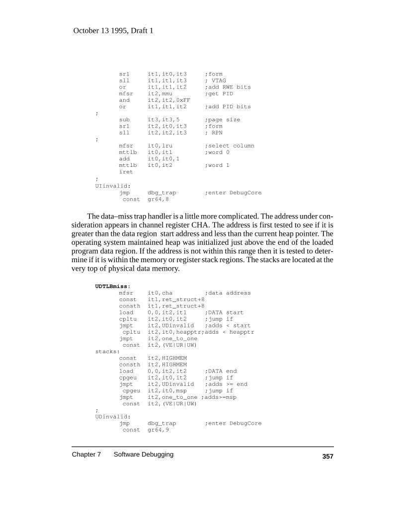
October 13 1995, Draft 1
357Chapter 7 Software Debugging
srl it1,it0,it3 ;formsll it1,it1,it3 ; VTAGor it1,it1,it2 ;add RWE bitsmfsr it2,mmu ;get PIDand it2,it2,0xFFor it1,it1,it2 ;add PID bits
;sub it3,it3,5 ;page sizesrl it2,it0,it3 ;form sll it2,it2,it3 ; RPN
;mfsr it0,lru ;select columnmttlb it0,it1 ;word 0add it0,it0,1mttlb it0,it2 ;word 1iret
;UIinvalid:
jmp dbg_trap ;enter DebugCore const gr64,8
The data–miss trap handler is a little more complicated. The address under con-sideration appears in channel register CHA. The address is first tested to see if it isgreater than the data region start address and less than the current heap pointer. Theoperating system maintained heap was initialized just above the end of the loadedprogram data region. If the address is not within this range then it is tested to deter-mine if it is within the memory or register stack regions. The stacks are located at thevery top of physical data memory.
UDTLBmiss:mfsr it0,cha ;data addressconst it1,ret_struct+8consth it1,ret_struct+8load 0,0,it2,it1 ;DATA startcpltu it2,it0,it2 ;jump ifjmpt it2,UDinvalid ;adds < start cpltu it2,it0,heapptr;adds < heapptrjmpt it2,one_to_one const it2,(VE|UR|UW)
stacks:const it2,HIGHMEMconsth it2,HIGHMEMload 0,0,it2,it2 ;DATA endcpgeu it2,it0,it2 ;jump ifjmpt it2,UDinvalid ;adds >= end cpgeu it2,it0,msp ;jump ifjmpt it2,one_to_one ;adds>=msp const it2,(VE|UR|UW)
;UDinvalid:
jmp dbg_trap ;enter DebugCore const gr64,9

October 13 1995, Draft 1
358 Addendum to –– Evaluating and Programming the 29K RISC Family
The example trap handler marks data pages for read and write access only. If theCHA address does not fall within the allowed region, then a TLB entry is not built,and, normally, program execution not restarted. Instead, the DebugCore is enteredand the trap number passed.
7.4.6 Down Loading a New OS
One way to replace OS–boot with another operating system is to simply link thenew operating system with the MiniMON29K modules and, if necessary, place theresult in EPROM memory. Or alternatively down–load the linked image to the target29K system using MiniMON29K messages. However, many users like to keep theexisting OS–boot/MiniMON29K combination in place and down–load only the newoperating system (or a portion of it) –– this can create complications. Assuming nochanges are made to the supplied OS–boot, then, when the loaded OS’s execution isstarted, with say a MonDFE ‘g’ command, warm–start code will prepare for execu-tion to begin at the first instruction of the new operating system. Generally a HIF se-trap service call is made followed by an assertion of the assigned trap number. Thisallows Supervisor mode to be entered.
The new operating system must initially run in Supervisor mode to take overprocessor resources initially under OS–boot control. If the floating–point trap han-dlers are to remain installed, then the new operating system must be careful to re-member their global register support requirement. If the new operating system is stillsupporting HIF services then it must also pay attention to the HIF trapware registerusage. HIF traps will occur if any application code run by the new OS is linked withlibraries intended for use with a HIF conforming operating system. However, often anew operating system will replace the HIF libraries with new libraries which do notcall HIF, but make use of the system call services of the new operating system.
The HIF trapware code can be replaced with new code, whose register usage isbetter integrated with the new operating system, by the new system taking over theHIF vector table entry. If this is done, then it is likely that the operating system mes-sage interrupt handler will also be taken over. Unless the os_V_msg trap handler ad-dress is replaced, the message system will continue to call the OS–boot interrupt han-dler. And the associated operating system register usage should be taken into ac-count. Alternatively, AMD supplies driver routines which make it easy for a new op-erating system to use the original message system for standard input and output com-munication. This eliminates the need for the new OS to to takeover the message sys-tem interrupt handlers.
The MiniMON29K message system is typically supported by low level drivercode which is often interrupt driven. Most often this is a UART interrupt handler. Themessage system will not generate virtual interrupts if the low level handler vectortable entry is taken over. This can be necessary because of interrupt overloading. Forexample, the Am29200 interrupt INTR3 is used for all peripheral devices including

October 13 1995, Draft 1
359Chapter 7 Software Debugging
the on–chip UART. A new operating system may wish to add support, for say, DMAactivity, which was not supported by OS–boot. This may require an interrupt handleractivated by INTR3. If the MiniMON29K message system is to continue operation,then the new operating system must take over the INTR3 vector table entry. But, afterthe new operating system handler is complete it must jump to the original vector han-dler address rather than IRETing. This gives the message system low level interrupthandler an opportunity to run. A better alternative is to use the technique described insection 2.5.5 to deal with INTR3 overloading.
7.5 UNIVERSAL DEBUG INTERFACE (UDI)
Code development for an embedded processor is generally more costly than de-velopment of code of equivalent complexity intended for execution on a engineeringworkstation. The embedded application code can not benefit from an underlying sup-port operating system such as UNIX. In some cases, developers may chose to firstinstall a small debug support monitor, such as MiniMON29K, or third–party execu-tive which can offer a somewhat improved development environment. In the processof getting an embedded support monitor running or developing application code torun directly on the processor, emulation hardware may be employed. The availabilityof debug tools and their configurability is an important factor when selecting a pro-cessor for an embedded project.
The architecture of the latest RISC processors may be simplified compared totheir CISC predecessors, but the complexity of controlling the processor operationhas not been reduced. The use of register stacks and instruction delay slots and otherperformance enhancing techniques has lead to increased use of high level program-ming languages such as C. The compiler has been given the responsibility of produc-ing efficient assembly code, and the developer rarely deals with code which manipu-lates data at the processor register level. The increased productivity achievable bythis approach is dependent on high level debug support tools.
Developers of products containing embedded processors are looking to RISCfor future products offering increased capability. The greater performance relative toRISC processor cost should make this possible. The suitability, cost and productivityof the tools available for code development are likely to be the major factor in decid-ing the direction ahead in preparing to tool–up for RISC.
The following sections describe the Universal Debug Interface (UDI), which isprocessor independent and enables greater debug tool configurability. A number ofemulator and embedded monitor suppliers, as well as high level language debugtools suppliers, are currently configuring their tools to comply with the proposedUDI standard. Current implementations are targeted for RISC processor code devel-opment. UDI should ease the choice in selecting tools and, consequently, selectingRISC. This section shall concentrate on describing the Free Software Foundation’sGDB C language source debugger’s integration with UDI.
October 13 1995, Draft 1
360 Addendum to –– Evaluating and Programming the 29K RISC Family
7.5.1 Debug Tool Developers
A debug tool developer typically arranges for their product to be available for arange of popular processors. This normally means rebuilding the tool with the knowl-edge required to understand the peculiarities of each processor. If an enhancement ismade to the debugger user–interface, then normally the debugger source and the pro-cessor specific information must be recompiled and tested before customers are up-dated.
When developing code to run on an engineering workstation, the processor sup-porting the debugger execution is the same processor running the program being de-veloped. This means the debugger can make use of operating system services such asptrace() (see section 7.5.3), to examine and control the program being debugged.When developing code for an embedded application, the program being developed isknown as the Target Program and executes on the Target Processor which is usually adifferent processor than the one supporting the debugger, known as the Host Proces-sor. The host processor and target processor do not communicate via the ptrace() sys-tem call, but via whatever hardware communication path links the two processors.The portion of the debugger which controls communication with the target processoris known as the target interface module, and whenever a change or addition is re-quired in the communications mechanism, the debugger must be once again recom-piled to produce a binary executable which is specific to the target–processor and tar-get–communications requirements.
When the chipmakers turn out their latest whiz–bang RISC processor, the tooldeveloper companies are faced with considerable development costs in ensuringtheir tools function with the new architecture. It is not uncommon for the availabilityof debug tools to lag behind RISC chip introduction. Often tools are introduced withlimited configuration options. For example, target processor communication may beaccording to a low level debug monitor protocol, or an in–circuit emulator (ICE) pro-tocol. Each debugger product has its own target interface module; this module mustbe developed for each debugger in order to communicate with the new target RISCprocessor.
An embedded application developer may have prior experience or a preferencefor a particular debug tool, but the only available communications path to the targetmay not be currently supported. This incompatibility may discourage the developerfrom choosing to use a new processor. It is desirable that debuggers share commu-nication modules and be more adaptable to available target processor interfaces.
Ideally a debugger from one company should be able to operate with, say, anemulator from another company. This would make it possible for a customer to selecta little used debugger with a popular target monitor or vice versa.
The goal of the Universal Debug Interface (UDI) is to provide a standard inter-face between the debugger developer and the target communications module, so thetwo can be developed and supplied separately. In fact, an applications developer

October 13 1995, Draft 1
361Chapter 7 Software Debugging
could construct their own communications module, for some special hardware com-munications link, as long as it complied with the standard.
7.5.2 UDI Specification
If UDI were a specification at procedural level, then debugger developers andcommunication module developers would have to supply linkable images of theircode so the debug tool combination could be linked by the intended user. This is un-desirable because it would require a linked image for every tool combination. Addi-tionally, the final linked program would be required to run on an single debug host.UDI actually relies on an interprocess communication (IPC) mechanism to connecttwo different processes. The debugger is linked into an executable program to run onthe host processor, this process is known as the Debugger Front End (DFE). The com-munications module is linked as a separate process which runs on the same or a dif-ferent host processor, this process is known as the Target interface Process(TIP). Thetwo processes communicate via the UDI interprocess communication specification.
Two IPC mechanisms have so far been specified: one uses shared memory and isintended for DOS developers, the second uses sockets and is intended for UNIX andVMS developers. Of course, when the shared memory IPC implementation is usedthe DFE and TIP processes must both execute on the same host processor. Usingsockets with Internet domain communication enables the DFE and TIP to eachexecute on separate hosts on a computer network. Thus an applications developercan, from the workstation on his desk, debug a target processor which is connected toa network node located in a remote hardware lab. Using sockets with UNIX domainaddresses (the method used to implement UNIX pipes) enables both processes to runon the same host.
Some of the currently available UDI conforming debug tools are presented inFigure 7-9. The interprocess communications layer defined by UDI enables the ap-plications developer to select any front end tool (DFE) with any of the target controltools (TIP).
Because developers of UDI conforming tools must each have code which inter-faces with the IPC mechanism according to the UDI protocol, the UDI communityfreely shares a library of code know as the UDI–p library. This code presents a proce-dural layer which hides the IPC implementation. For example, consider the follow-ing procedure:
The DFE code calls the UDIRead function which transports the function call tothe TIP process. The TIP code developer must resolve the function request, by addingcode which is specific to controlling the particular target. The IPC layer is effectivelytransparent, the TIP developer is unaware that the procedure caller is from a differentprocess, possibly on a different host machine. Table 7-2 lists most of the UDI–p pro-cedures available.

October 13 1995, Draft 1
362 Addendum to –– Evaluating and Programming the 29K RISC Family
Figure 7-9. Currently Available Debugging Tools that Conform to UDI Specification
GDB source–leveldebugger
XRAY source–leveldebugger
SDB source–leveldebugger
MiniMON29K interfaceMonDFE
DebuggerFront–end Process
UDI–IPCLayer
Remote–targetInterface Process
ISS instructionISSTIP
ICE In–CircuitEmulator
MiniMON29KMonTIP
Emulator Pod
Target MonitorDebugCore
Emulator Cable
Private Link, maybe rs232optionalROM Emulator
UDB source–leveldebugger
Logic AnalyserHP16500B
Because the DFE and TIP processes may be running on different machines, caremust be taken when moving data objects between hosts. An “int” sized object on theDFE supporting machine may be a different size from an “int” on the TIP supportingmachine. Further, the machines may be of different endian. The UDI–p proceduresmake use of a machine independent data description technique similar to the XDRlibrary available with UNIX. Data is converted into a universal data representation(UDR) format before being transferred via sockets. On being received, the data isconverted from UDR format into data structures which are appropriate for the receiv-ing machine. The UDI–p procedures keep the UDR activity hidden from the UDIuser.

October 13 1995, Draft 1
363Chapter 7 Software Debugging
Table 7-2. UDI–p Procedures (Version 1.2)
Procedure Operation
UDIConnect Connect to selected TIPUDIDisconnect Disconnect from TIPUDISetCurrentConnection For multiple TIP selectionUDICapabilities Obtain DFE and TIP capability informationUDIEnumerateTIPs List multiple TIPs availableUDICreateProcess Load a program for debuggingUDISetCurrentProces Select from multiple loaded programsUDIDestroyProcess Discontinue program debuggingUDIInitializeProcess Prepare runtime environmentUDIRead Read data from target–processor memoryUDIWrite Write data to target–processor memoryUDICopy Duplicate a block of data in target memoryUDIExecute Start/continue target–processor executionUDIStep Execute the next instructionUDIStop Request the target to stop executionUDIWait Inquire about target statusUDISetBreakpoint Insert a breakpointUDIQueryBreakpoint Inquire about a breakpointUDIClearBreakpoint Remove a breakpoint
In later sections of this chapter, the development of a UDI conforming GDB, asource level debugger from the Free Software Foundation and Cygnus Support, isdiscussed in more detail. GDB is an example of a DFE process. As an example of aTIP process, we shall look at the MiniMON29K monitor and the Instruction Set Sim-ulator from AMD. Most users of GDB will have some knowledge of the ptrace()system call which enables GDB to examine the state of the process being debugged.A brief description of ptrace() is beneficial along with further explanation of its un-suitability for embedded application software development.
7.5.3 P–trace
UNIX system call, ptrace(), provides a means by which a process may controlthe execution of another process executing on the same processor. The process beingdebugged is said to be “traced”. However, this does not mean that the execution pathof a process is recorded in a “trace buffer” as is the case with many processor emula-tors. Debugging with ptrace() relies on the use of instruction breakpoints and otherhardware or processor generated signals causing execution to stop.
ptrace(request, pid, addr, data)
There are four arguments whose interpretation depends on the request argu-ment. Generally, pid is the process ID of the traced process. A process being de-bugged behaves normally until it encounters some signal whether internally (proces-

October 13 1995, Draft 1
364 Addendum to –– Evaluating and Programming the 29K RISC Family
sor) generated, like illegal instruction, or externally generated, like interrupt. Thenthe traced process enters a stopped state and the tracing process is notified using thewait() system call. When the traced process is in the stopped state, its core image canbe examined and modified using the ptrace() service. If desired, another ptrace() re-quest can then cause the traced process either to terminate or to continue. Table 7-3lists the ptrace() request services available.
Table 7-3. ptrace() Services
Request Operation
TraceMe Declare that the process is being tracedPeekText Read one word in the process’s instruction spacePeekData Read one word in the proceses’s data spacePeekUser Examine the processes–control data structurePokeText Write one word in process’s text spacePokeDate Write one word in process’s data spacePokeUser Write one word in process–control data structureCont Startup process executionKill Terminate the process being debuggedSingleStep Execute the next instructionGetRegs Read processor registerSetRegs Write processor registerReadText Read data from process’s instruction spaceReadData Read data from process’s data spaceWriteText Write data into process’s instruction spaceWriteData Write data into process’s data spaceSysCall Continue execution until system call
Because both the process with the user–interface controlling the debugging, andthe application process being debugged, may not be executing on the same processor,it is not possible to use the ptrace() system call mechanism to debug embedded ap-plication software. The debugger process (DFE) must run on a separate processorand communicate with the processor supporting execution of the application code.
The Free Software Foundation’s source level debugger, GDB, makes use of theptrace() system call. However, it can alternatively use a collection of procedureswhich support communication to a remote processor. These procedures implementthe necessary protocols to control the hardware connecting the remote processor tothe “host” debug processor. By this means, GDB can be used to debug embedded ap-plication software running on application specific hardware. The following sectiondiscusses the method in more detail.
7.5.4 The GDB–UDI Connection
GDB can, in place of ptrace(), make use of a procedural interface which allowscommunication with a remote target processor. Newer versions of GDB (version3.98 and later) achieve this via procedure pointers which are members of a target_ops

October 13 1995, Draft 1
365Chapter 7 Software Debugging
structure. The procedures currently available are listed in Table 7-4. According toGDB configuration convention, the file remote–udi.c must be used to implement theremote interface procedures. In the case of interfacing to the IPC mechanism used byUDI, the procedures in Table 7-4 are mapped into the UDI–p procedures given inTable 7-2. With the availability of the UDI–p library, it is a simple task to map theGDB remote interface procedures for socket communication with a remote targetprocessor.
Table 7-4. GDB Remote–Target Operations
Function Operation
to_open() Open communication connection to remote targetto_close() Close connection to remote targetto_attach() Attach to a loaded and running programto_detach() Detach for multitarget debuggingto_start() Load program into target–system memoryto_wait() Wait until target–system execution stopsto_resume() Startup/Continue target–system executionto_fetch_register() Read target–system processor register(s)to_store_register() Write register(s) in target–system processorto_xfer_memory() Read/Write data to target–system memoryto_insert_breakpoint() Establish an instruction break addressto_remove_breakpoint() Remove a breakpointto_load() Load a program into target–processor memory
7.5.5 The UDI–MiniMON29K Monitor Connection, MonTIP
MiniMON29K monitor code can not function without the support of a softwaremodule located in a support processor; the software module is known as the targetinterface process (TIP). The 29K target processor communicates with the processorrunning the TIP process via a serial link or other higher performance channel. Thislink supports a message system which is private to the MiniMON29K monitor, bythat I mean it is completely independent of the UDI protocol. (See Figure 7-2.)
MiniMON29K must be installed in target system ROM memory or down–loaded by the TIP host via a shared memory interface. The target application code,and additional operating system code, can then be down–loaded via the message sys-tem. If changes to the code are required, then the message system can be used toquickly down–load new code without changing any ROM devices.
The MiniMON29K TIP process, montip, converts UDI service requests intoMiniMON29K messages. The montip program which runs on UNIX machines, typ-ically communicates with the target using an rs232 link. When run on DOS ma-chines, it may communicate using an rs232 connection or a PC plug–in board sharedmemory scheme. Note, UNIX machines can be also used to debug PC plug–in cards;the pcserver program, run on DOS machines, enables the PC serial port to be con-
October 13 1995, Draft 1
366 Addendum to –– Evaluating and Programming the 29K RISC Family
nected to a UNIX machine. The MiniMON29K messages, transferred to the DOShost via plug–in card shared memory, are sent to the TIP host via the rs232 connec-tion. The montip program supports several command–line options, as shown below.Not all are applicable to both DOS and UNIX host machines.montip –t target [–r OS–boot] [–m msg_log] [–com serial_port]
[–re msg_retries] [–mbuf msg_bufsize] [–bl msg_loopcount][–to timeout] [–seg PC_seg_addr] [–port PC_port_base][–baud baudrate] [–le] [–R|P]
A explanation of the command line options can be obtained by just enteringmontip on your TIP host machine. When the montip process is started it advertisesits readiness to service UDI requests. A DFE process will typically connect to theTIP process and a debug session will commence. Alternatively, there is no need tofirst start the TIP process. When a DFE process is started, such as mondfe, it will lookfor the advertised TIP; if the TIP process is not found the DFE will automatically startthe TIP. This is how montip is normally started. The start–up montip parameters aretaken from the “UDI Configuration File”. The format of this file is explained in thefollowing section discussing mondfe.
7.5.6 The MiniMON29K User–Interface, MonDFE
The MiniMON29K DFE process, mondfe, is a primitive 29K debugger. It pro-vides a basic user–interface for the MiniMON29K product. It is fully UDI compliant(at least UDI version 1.2 ); and it can be used with any of the available TIP processessuch as isstip, mtip , montip, etc. It is very easy to operate but has less debuggingcapability compared to other DFEs, such as gdb, xray29u or UDB (see section 7.7)etc.; for example it does not support symbolic debugging.
It is very useful for simply loading application programs and starting theirexecution where no debugging support is required. Its simple command set alsomakes it easy to learn; when running, simply type the h command to obtain a com-plete list of available commands. The h command can also be used to explain eachcommand’s operation; for example, “h s” will explain the operation of the set com-mand. Several command–line options are supported.
mondfe [–D] –TIP tip_id [–q] [–e echo_file] [–c command_file][–ms mem_stack_size] [–rs reg_stack_size] [–le] [–log logfile] [pgm_name [arg_list]]
A list of command line options can be had by entering mondfe on your DFE hostprocessor. The process is typically started by entering a command such as “modfe–D –TIP serial”. The “–D” option causes an interactive debug session to commence.The UDI conforming TIP process communicating with mondfe is identified by the“–TIP serial” command line option.
DFEs and TIPs establish communication via a UDI Configuration File. OnUNIX machines this file is called udi_soc; on DOS machines it is called udiconfs.txt.
October 13 1995, Draft 1
367Chapter 7 Software Debugging
The Configuration File is found by first looking in the current working directory. Ifnot found, the file given by environment variable UDICONF is searched for. Lastly,the executable PATH is searched. The format of these files is very similar, on UNIX:
session_id AF_UNIX socket_name tip_exe tip_parameterssession_id AF_INET host_name port <not required>
The first column gives the session_id, which is used to select the appropriateline. The serial key–word used with the “–TIP” option in the example, is comparedwith the session_id for each line in the Configuration File. The first matching lineprovides all the necessary data for connecting to a TIP process which is already run-ning; or, if necessary, starting TIP process execution.
The second column gives the socket domain used by the socket IPC mechanismconnecting the two processes. Two domains are supported. The AF_UNIX domainindicates both processes reside on the same host processor. Use of the AF_INET do-main indicates the TIP process is on another networked host machine. In such a case,the host name and socket port number are supplied in the following columns. TheUDI specification does not support DFEs starting TIP processes on remote hosts.When the AF_INET domain is used to connect to the TIP, the TIP process must befirst up and running before connection is attempted.
When the AF_UNIX domain is used, the third column gives the name of thesocket used by the TIP to advertise its UDI services. If the DFE is unable to connect tothe named socket, it will assume the TIP is not running. In such a case the remainingline information gives the name of the TIP executable and the start–up parameters.Below is example udi_soc file contents.
mon AF_UNIX mon_soc montip –t serial –baud 38400 –com /dev/ttyaserial AF_UNIX * montip –t serial –baud 9600 –com /dev/ttyaiss AF_UNIX iss_soc iss –r ../../src/osboot/sim/osbootpcserver AF_UNIX pc_soc pcserver –t serial –baud 9600 –com /dev/ttyacruncher AF_INET hotbox 7000netrom AF_UNIX net_soc montip –t netrom –netaddr 163.181.22.41 ...
The relative path names given with montip start–up parameters, are relative to:<montip executable directory>/../lib . The path given with the “–r” option is requiredto find the OS–boot code for 29K start–up. When the DFE is always used to automati-cally start the TIP process, a “*” can be used for the socket name field. This causes theDFE to generate a random name for the socket file. This file will be removed whenthe DFE and TIP discontinue execution at the end of the debug session.
The DOS Configuration File (udiconfs.txt) format is a little simpler. There areonly three entry fields, as shown by the example below:

October 13 1995, Draft 1
368 Addendum to –– Evaluating and Programming the 29K RISC Family
mon montip.exe –t serial –baud 38400serial montip.exe –t serial –baud 9600sim iss.exe –r ..\..\src\osboot\sim\osbooteb29K montip.exe –t eb29K –r ..\..\src\minimon\eb29K\mon.oyarcrev8 montip.exe –t yarcrev8 –r ..\..\src\minimon\yarcrev8\mon.os
The first field is again the session identifier. The second and third fields containthe TIP executable file name and its start–up option switches. All DFEs have somekind of command–line or interactive command which allows the session_id value tobe entered. The DFE then reads the UDI Configuration File to determine the TIP withwhich communication is to be established. Most DFEs (mondfe has the disc com-mand) have a command which enables the DFE to disconnect from the TIP, cease toexecute but leave the TIP running. Because the TIP is still alive and ready to serviceUDI requests, a DFE can start–up later and reconnect with the TIP. However, typical-ly the DFE and TIP processes are terminated at the same time.
7.5.7 The UDI – Instruction Set Simulator Connection, ISSTIP
An Instruction Set Simulator, isstip, is available for DOS and UNIX type hosts.The isstip process is fully UDI conforming and can be used by any DFE. Because ofexisting contract limitations, AMD normally ships isstip in binary rather than sourceform. Using the simulator along with, say the gdb DFE, is a convenient and powerfulway of exercising 29K code without ever having to build hardware. Thus, softwareengineers can use the simulator while a project’s hardware is still being debugged.
The Instruction Set Simulator can not be used for accurate application bench-marking, as the system memory model can not be incorporated into the simulation.AMD supplies the architectural simulator, sim29, for that purpose (see Chapter 1).The simulator supports several command line options, as shown below. For an ex-planation of these options, enter isstip or man isstip, on your TIP host machine.
isstip [–r osboot_file] [–29000|–29050|–29030|–29200] [–t] [–tm][–id <0|1>] [–sp <0|1>] [–st <hexaddr>] [–ww] [–le] [–p|v]
With the –r option, the osboot_file is loaded into memory at address 0. This isuseful for installing operating systems like OS–boot before application code startsexecuting. With processors which support separate Instruction and ROM memoryspaces, the osboot_file is loaded into ROM space. If the –r option is not used, the sim-ulator will intercept HIF service calls and perform the necessary operating systemsupport service. The simulator always intercepts HIF services with service numbers255 and less regardless of the –r option. These HIF services are provided directly bythe simulator.
The simulator is very useful for debugging Freeze mode code. It will allowsingle stepping through Freeze mode code which is not possible with a real processorunless it supports Monitor mode. Freeze mode code is normally supplied in the op-

October 13 1995, Draft 1
369Chapter 7 Software Debugging
tional osboot_file. Thus, the –r option must be used to enable Freeze mode debug-ging. Additionally, to enable debugging of Freeze mode timer interrupts the –tm op-tion must also be selected to enable timer interrupt simulation. The simulator normal-ly intercepts floating–point traps and performs the necessary calculation directly.Simulation speeds are reduced if floating–point trapware is simulated. However, ifthe trapware is to be debugged the –t option must be used to enable trapware simula-tion.
When the isstip process is started it advertises its readiness to service UDI re-quests. A DFE process will typically connect to the TIP process and a debug sessionwill commence. However, it is more typical to get the DFE to start the TIP. Themondfe process starts the TIP during the DFE start–up process. The gdb DFE startsthe TIP after the target gdb command is used. The start–up isstip parameters are tak-en from the “UDI Configuration File”. The format of this file is explained in the pre-vious section discussing mondfe.
7.5.8 UDI Benefits
A number of debug tool developers are currently, or will be shortly, offeringtools which are UDI compliant. Typically the DFEs are C source level debuggers.This is not surprising, as the increased use of RISC processor designs has resulted in acorresponding increase in software complexity. The use of a high level language,such as C, is more productive than developing code at machine instruction level. Andfurther, the use of C enables much greater portability of code among current andfuture projects. The low cost of GDB makes it an attractive choice for developers.
Target processors and their control mechanisms are much more varied thanDebugger Front Ends (DFEs). I have briefly described the MiniMON29K TIP, whichis a process which controls the execution of a 29K processor. A small amount of codeknown as the DebugCore is placed in processor ROM memory and enablesexamination of the processor state. The MiniMON29K TIP communicates with theDebugCore via a hardware link which is specific to the embedded applicationhardware.
Other TIPs already exist and more are under development. There is a 29Ksimulator (ISS) which runs on UNIX and DOS hosts. The DFE communicating withthe simulator TIP is unaware that the 29K processor is not present, but beingsimulated by a process, executing on, say, a UNIX workstation. There are also tooldevelopers constructing TIP programs to control processor emulators. This willmake possible a top–of–the–line debug environment.
UDI makes possible a wider tool choice for application code developers.Debugger front end tools are supplied separately from target control programs. Theuser can consider cost, availability and functionality when selecting the debugenvironment. This level of debug tool configurability has not been available to theembedded application development community in the past.

October 13 1995, Draft 1
370 Addendum to –– Evaluating and Programming the 29K RISC Family
Because debuggers like GDB are available in source form, developers can addadditional debug commands, such as examination of real–time operating systemperformance. This would require adding operating system structural informationinto GDB. When the debugger front end and, for example, an emulator interfacemodule, are supplied as a single executable, adding new commands is not possible.Via the use of Internet sockets the debugger may execute on a different networkedhost than the node supporting the emulator control process.
7.5.9 Getting Started with GDB
To demonstrate the operation of GDB debugging a program running on anAm29000 processor, the program below was compiled using the Free SoftwareFoundation’s GCC compiler. The example is simple, but it does help to understandthe GDB–MiniMON29K monitor debug mechanism. A stand–alone Am29000processor development card was used. It contains a UART and space for RAM andEPROM devices. The MiniMON29K monitor modules were linked with a HIFoperating system support module (OS–boot) and an Am85C30 UART messagedriver module [AMD 1988]. The linked image was installed in EPROM devices inthe target hardware. A serial cable was then used to connected the UART to a port on aSUN–3/80 workstation.
The demonstration could have been equally as well been performed on a386–based IBM–PC; the target hardware being connected via a PC serial port.Alternatively, there are a number of manufactures building evaluation cards whichsupport a dual–ported memory located on a PC plug–in card containing the RISCprocessor. The 386 communicates with the target processor via a shared memoryinterface. This requires a TIP which can communicate via shared memory with theDebugCore running on the target hardware. A number of such TIP control processeshave been built. A board developer has only to implement the TIP portion of thedebug mechanism to gain access to a number of debuggers such as GDB which areUDI conforming. Note, due to an implementation limitation of the current DOSversion of GDB, it is necessary to start the TIP process manually. GDB is unable toautomatically start the montip or isstip. The command shown below most be used tostart montip on a DOS host before GDB can communicate with the target 29Ksystem.
montip montip.exe
The demonstration program, listed below, simply measures the number of char-acters in the string supplied as a parameter to the main() function.
main(argc, argv) /* program measure.c */int argc;char *argv[];{

October 13 1995, Draft 1
371Chapter 7 Software Debugging
int len;if(argc < 2) return;len = strlen(argv[1]);
printf(”length=%d\en”, len);}
int strlen(s)char *s;{
int n;for (n = 0; *s != ’\0’; s++)n++;return(n);
}
GDB was started running on the UNIX machine. The target command was usedto establish communication with the DebugCore running in the standalone develop-ment card. The UDI Configuration file was used to establish DFE and TIP commu-nication. The format of the Configuration File was described in section 7.5.6. TheUDI session_id for the example shown is monitor. The list below presents the re-sponse seen by the user. The keyboard entries made by the user are shown in boldtype.
gdbGDB is free software and you are welcome to distribute copies ofit under certain conditions; type ”show copying” to see theconditions. There is absolutely no warranty for GDB; type ”showwarranty” for details. GDB 4.5.2, Copyright 1992 Free SoftwareFoundation, Inc.
(gdb) target udi monitor measureRemote debugging Am29000 rev D Remote debugging an Am29000connected via UDI socket, DFE–IPC version 1.2.1 TIP–IPC version1.2.1 TIP version 2.5.1 MONTIP UDI 1.2 Conformant
Once communication had been established, a breakpoint was set at the entry tothe strlen() function. Execution was then started using the run command. GDB in-forms the user that the program is being loaded. This is accomplished by the TIPsending messages to the debug core, which transfers the accompanying message datainto Am29000 processor memory before Am29000 processor execution com-mences.
(gdb) symbol measureReading in symbols for measure.c...done.
(gdb) break strlenBreakpoint 1 at 0x10200: file measure.c, line 14.

October 13 1995, Draft 1
372 Addendum to –– Evaluating and Programming the 29K RISC Family
(gdb) run measure_my_lengthLoading TEXT section at 0x10000 (24408 bytes) ...Loading DATA section at 0x80003000 (4096 bytes) ...Clearing BSS section at 0x80004000 (0 bytes) ...Breakpoint 1, strlen(s=0x80004013 ”measure_my_length”)
(measure.c line 1717 for (n = 0; *s != ’\0’; s++)
The program runs until the requested breakpoint is encountered. At this point asource code listing was requested. Typically, debug monitors do not allow sourcecode to be viewed. The use of GDB makes this important advantage available to theembedded software developer.
(gdb) list1112 int strlen(s)13 char *s;14 {15 int n;1617 for (n = 0; *s != ’\0’; s++)18 n++;19 return (n);20 }
The user then examined the call–stack history using the info stack command.This is currently inefficiently implemented. GDB uses the to_xfer_memory() proce-dure to send read messages to the target DebugCore. Examining the instructionmemory in this way is much less efficient than requesting the DebugCore to searchback through its own memory for procedural tag words. Each procedure has a non–executable trace–back tag word, or two, placed before the first instruction of the pro-cedure (see Chapter 3). Tag words enable debuggers to quickly gain informationabout a procedure frame, and hence variable values. Adding the procedural “hook” toGDB to make use of the MiniMON29K monitor FIND service would greatly reducemessage traffic, and improve the users response time for the info stack command.
(gdb) info stack#0 strlen (s=0x80004013 ”measure_my_length”) (measure.c line 17)#1 0x101ac in main (argc=2, argv=0x80004000) (measure.c line 8)
GDB enables single stepping of source code with the step or next commands.The listing shows a source–level step request followed by the printing of proceduralvariables “n” and “s”. With large embedded programs it is important to be able to de-bug at source–level, and examine variables without having to look at cross–listingmapping tables to find the address associated with a variables memory location. Typ-ically small embedded debug monitors do not support this kind of debugging.
(gdb) step17 for (n = 0; *s != ’\0’; s++)
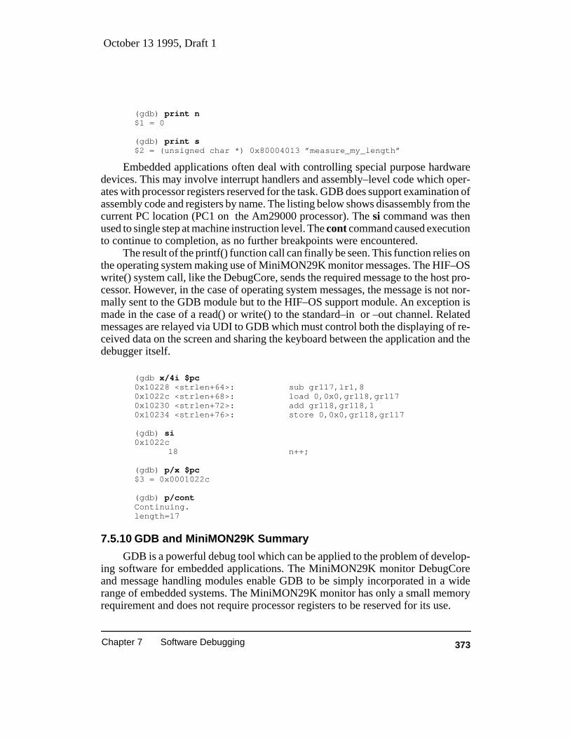
October 13 1995, Draft 1
373Chapter 7 Software Debugging
(gdb) print n$1 = 0
(gdb) print s$2 = (unsigned char *) 0x80004013 ”measure_my_length”
Embedded applications often deal with controlling special purpose hardwaredevices. This may involve interrupt handlers and assembly–level code which oper-ates with processor registers reserved for the task. GDB does support examination ofassembly code and registers by name. The listing below shows disassembly from thecurrent PC location (PC1 on the Am29000 processor). The si command was thenused to single step at machine instruction level. The cont command caused executionto continue to completion, as no further breakpoints were encountered.
The result of the printf() function call can finally be seen. This function relies onthe operating system making use of MiniMON29K monitor messages. The HIF–OSwrite() system call, like the DebugCore, sends the required message to the host pro-cessor. However, in the case of operating system messages, the message is not nor-mally sent to the GDB module but to the HIF–OS support module. An exception ismade in the case of a read() or write() to the standard–in or –out channel. Relatedmessages are relayed via UDI to GDB which must control both the displaying of re-ceived data on the screen and sharing the keyboard between the application and thedebugger itself.
(gdb x/4i $pc0x10228 <strlen+64>: sub gr117,lr1,80x1022c <strlen+68>: load 0,0x0,gr118,gr1170x10230 <strlen+72>: add gr118,gr118,10x10234 <strlen+76>: store 0,0x0,gr118,gr117
(gdb) si0x1022c
18 n++;
(gdb) p/x $pc$3 = 0x0001022c
(gdb) p/contContinuing.length=17
7.5.10 GDB and MiniMON29K Summary
GDB is a powerful debug tool which can be applied to the problem of develop-ing software for embedded applications. The MiniMON29K monitor DebugCoreand message handling modules enable GDB to be simply incorporated in a widerange of embedded systems. The MiniMON29K monitor has only a small memoryrequirement and does not require processor registers to be reserved for its use.
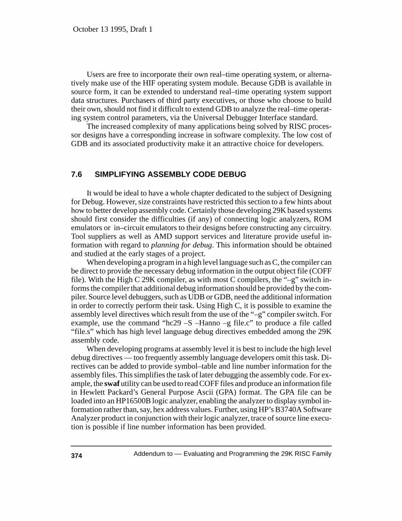
October 13 1995, Draft 1
374 Addendum to –– Evaluating and Programming the 29K RISC Family
Users are free to incorporate their own real–time operating system, or alterna-tively make use of the HIF operating system module. Because GDB is available insource form, it can be extended to understand real–time operating system supportdata structures. Purchasers of third party executives, or those who choose to buildtheir own, should not find it difficult to extend GDB to analyze the real–time operat-ing system control parameters, via the Universal Debugger Interface standard.
The increased complexity of many applications being solved by RISC proces-sor designs have a corresponding increase in software complexity. The low cost ofGDB and its associated productivity make it an attractive choice for developers.
7.6 SIMPLIFYING ASSEMBLY CODE DEBUG
It would be ideal to have a whole chapter dedicated to the subject of Designingfor Debug. However, size constraints have restricted this section to a few hints abouthow to better develop assembly code. Certainly those developing 29K based systemsshould first consider the difficulties (if any) of connecting logic analyzers, ROMemulators or in–circuit emulators to their designs before constructing any circuitry.Tool suppliers as well as AMD support services and literature provide useful in-formation with regard to planning for debug. This information should be obtainedand studied at the early stages of a project.
When developing a program in a high level language such as C, the compiler canbe direct to provide the necessary debug information in the output object file (COFFfile). With the High C 29K compiler, as with most C compilers, the “–g” switch in-forms the compiler that additional debug information should be provided by the com-piler. Source level debuggers, such as UDB or GDB, need the additional informationin order to correctly perform their task. Using High C, it is possible to examine theassembly level directives which result from the use of the “–g” compiler switch. Forexample, use the command “hc29 –S –Hanno –g file.c” to produce a file called“file.s” which has high level language debug directives embedded among the 29Kassembly code.
When developing programs at assembly level it is best to include the high leveldebug directives –– too frequently assembly language developers omit this task. Di-rectives can be added to provide symbol–table and line number information for theassembly files. This simplifies the task of later debugging the assembly code. For ex-ample, the swaf utility can be used to read COFF files and produce an information filein Hewlett Packard’s General Purpose Ascii (GPA) format. The GPA file can beloaded into an HP16500B logic analyzer, enabling the analyzer to display symbol in-formation rather than, say, hex address values. Further, using HP’s B3740A SoftwareAnalyzer product in conjunction with their logic analyzer, trace of source line execu-tion is possible if line number information has been provided.
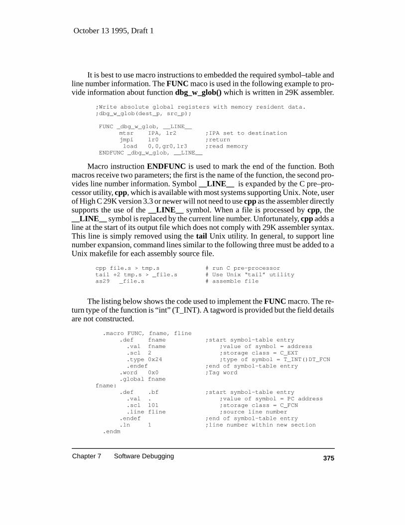
October 13 1995, Draft 1
375Chapter 7 Software Debugging
It is best to use macro instructions to embedded the required symbol–table andline number information. The FUNC maco is used in the following example to pro-vide information about function dbg_w_glob() which is written in 29K assembler.
;Write absolute global registers with memory resident data.;dbg_w_glob(dest_p, src_p);
FUNC _dbg_w_glob, __LINE__mtsr IPA, lr2 ;IPA set to destinationjmpi lr0 ;return load 0,0,gr0,lr3 ;read memory
ENDFUNC _dbg_w_glob, __LINE__
Macro instruction ENDFUNC is used to mark the end of the function. Bothmacros receive two parameters; the first is the name of the function, the second pro-vides line number information. Symbol __LINE__ is expanded by the C pre–pro-cessor utility, cpp, which is available with most systems supporting Unix. Note, userof High C 29K version 3.3 or newer will not need to use cpp as the assembler directlysupports the use of the __LINE__ symbol. When a file is processed by cpp, the__LINE__ symbol is replaced by the current line number. Unfortunately, cpp adds aline at the start of its output file which does not comply with 29K assembler syntax.This line is simply removed using the tail Unix utility. In general, to support linenumber expansion, command lines similar to the following three must be added to aUnix makefile for each assembly source file.
cpp file.s > tmp.s # run C pre–processortail +2 tmp.s > _file.s # Use Unix “tail” utilityas29 _file.s # assemble file
The listing below shows the code used to implement the FUNC macro. The re-turn type of the function is “int” (T_INT). A tagword is provided but the field detailsare not constructed.
.macro FUNC, fname, fline.def fname ;start symbol–table entry .val fname ;value of symbol = address .scl 2 ;storage class = C_EXT .type 0x24 ;type of symbol = T_INT()DT_FCN .endef ;end of symbol–table entry.word 0x0 ;Tag word.global fname
fname:.def .bf ;start symbol–table entry .val . ;value of symbol = PC address .scl 101 ;storage class = C_FCN .line fline ;source line number.endef ;end of symbol–table entry.ln 1 ;line number within new section
.endm
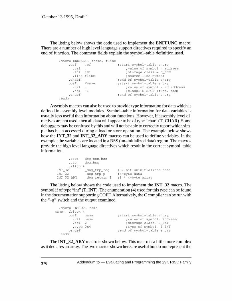
October 13 1995, Draft 1
376 Addendum to –– Evaluating and Programming the 29K RISC Family
The listing below shows the code used to implement the ENFFUNC macro.There are a number of high level language support directives required to specify anend of function. The comment fields explain the symbol–table definition used.
.macro ENDFUNC, fname, fline.def .ef ;start symbol–table entry .val . ;value of symbol = address .scl 101 ;storage class = C_FCN .line fline ;source line number.endef ;end of symbol–table entry.def fname ;start symbol–table entry .val . ;value of symbol = PC address .scl –1 ;class= C_EFCN (func. end).endef ;end of symbol–table entry
.endm
Assembly macros can also be used to provide type information for data which isdefined in assembly level modules. Symbol–table information for data variables isusually less useful than information about functions. However, if assembly level di-rectives are not used, then all data will appear to be of type “char” (T_CHAR). Somedebuggers may be confused by this and will not be able to correctly report which sim-ple has been accessed during a load or store operation. The example below showshow the INT_32 and INT_32_ARY macros can be used to define variables. In theexample, the variables are located in a BSS (un–initialized data) region. The macrosprovide the high level language directives which result in the correct symbol–tableinformation.
.sect dbg_bss,bss
.use dbg_bss
.align 4 INT_32 _dbg_tmp_reg ;32–bit uninitialised data INT_32 _dbg_tmp_p ;4–byte data INT_32_ARY _dbg_return,8 ;8 * 4–byte array
The listing below shows the code used to implement the INT_32 macro. Thesymbol if of type “int” (T_INT). The enumeration (4) used for this type can be foundin the documentation supporting COFF. Alternatively, the C compiler can be run withthe “–g” switch and the output examined.
.macro INT_32, namename: .block 4
.def name ;start symbol–table entry .val name ;value of symbol, address .scl 2 ;storage class, C_EXT .type 0x4 ;type of symbol, T_INT.endef ;end of symbol–table entry
.endm
The INT_32_ARY macro is shown below. This macro is a little more complexas it declares an array. The two macros shown here are useful but do not represent the
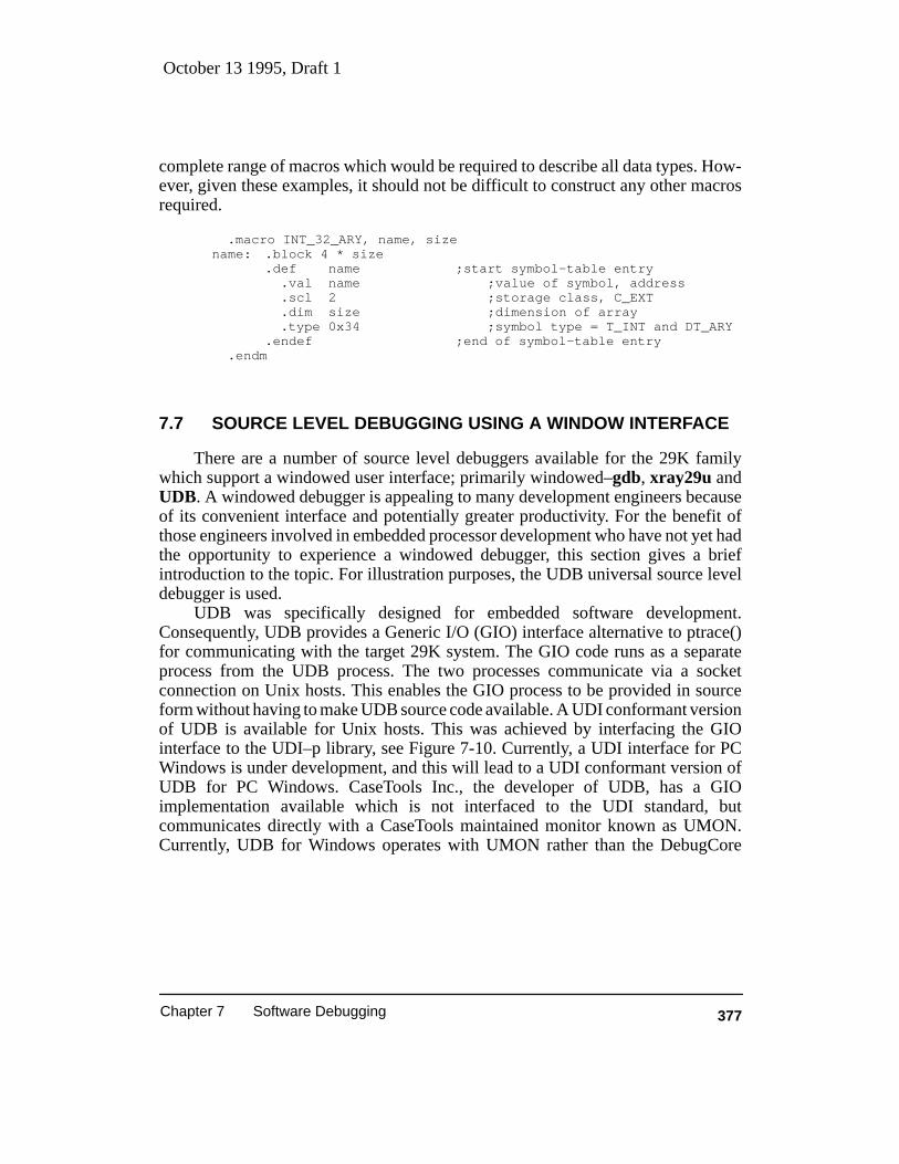
October 13 1995, Draft 1
377Chapter 7 Software Debugging
complete range of macros which would be required to describe all data types. How-ever, given these examples, it should not be difficult to construct any other macrosrequired.
.macro INT_32_ARY, name, sizename: .block 4 * size
.def name ;start symbol–table entry .val name ;value of symbol, address .scl 2 ;storage class, C_EXT .dim size ;dimension of array .type 0x34 ;symbol type = T_INT and DT_ARY.endef ;end of symbol–table entry
.endm
7.7 SOURCE LEVEL DEBUGGING USING A WINDOW INTERFACE
There are a number of source level debuggers available for the 29K familywhich support a windowed user interface; primarily windowed–gdb, xray29u andUDB. A windowed debugger is appealing to many development engineers becauseof its convenient interface and potentially greater productivity. For the benefit ofthose engineers involved in embedded processor development who have not yet hadthe opportunity to experience a windowed debugger, this section gives a briefintroduction to the topic. For illustration purposes, the UDB universal source leveldebugger is used.
UDB was specifically designed for embedded software development.Consequently, UDB provides a Generic I/O (GIO) interface alternative to ptrace()for communicating with the target 29K system. The GIO code runs as a separateprocess from the UDB process. The two processes communicate via a socketconnection on Unix hosts. This enables the GIO process to be provided in sourceform without having to make UDB source code available. A UDI conformant versionof UDB is available for Unix hosts. This was achieved by interfacing the GIOinterface to the UDI–p library, see Figure 7-10. Currently, a UDI interface for PCWindows is under development, and this will lead to a UDI conformant version ofUDB for PC Windows. CaseTools Inc., the developer of UDB, has a GIOimplementation available which is not interfaced to the UDI standard, butcommunicates directly with a CaseTools maintained monitor known as UMON.Currently, UDB for Windows operates with UMON rather than the DebugCore

October 13 1995, Draft 1
378 Addendum to –– Evaluating and Programming the 29K RISC Family
which is supplied as part of the MiniMON29K bundle. This will be the position untilthe UDI for PC Windows specification has been completed.
When a UDI conformant version of UDB is used with a 29K evaluation board,establishing UDB operation is very simple. The mktarget command in the udb.rcstart–up file is used to start a GIO processes which supports the UDI interface. TheGIO process uses the assigned mktarget parameters to select the entry in the udi_socfile which is then used to establish the DFE–TIP connection (see section 7.9.2). Inthis way, it is particularly convenient to use UDB with the instruction set simulatorISSTIP. Similarly, UDB can be configured to connect to MonTIP which itselfcommunicates, for example, via a serial link or NetROM (ROM emulator), to theDebugCore running in the 29K system.
Using UDB with UMON rather than MiniMON29K, is also simple when the29K evaluation board has UMON installed and running. CaseTools recommends thatUMON first be linked with 29K boot–up code know as boot–crt0 and then installedin, say, ROM on the target 29K system. A CaseTools customer is required toconstruct their own boot–crt0 code. This could be accomplished using the OS–bootcode provided by AMD.
However, because AMD provides 29K evaluation boards with MiniMON29Kalready installed, some developers and evaluators may wish to run UMON withoutfirst constructing a boot–crt0. The UMON monitor can be run on–top of theMiniMON29K DebugCore, and where necessary the application can make use ofservices provided by OS–boot in place of the missing boot–crt0. A number ofpreparation steps must be taken to make this tool combination operate correctly.These steps are explained below. It is important to remember these steps only applywhen launching UMON from MiniMON29K. No special linking and loading stepsare required if UDB is used directly with MiniMON29K or directly with UMONcombined with an appropriate boot–crt0.
Figure 7-10. The UDB to 29K Connection via the GIO Process
UDBDebug processrunning on DFEhost processor
MonTIPTarget–interfaceProcess on TIPhost processor
29K RISC withMiniMON29K
DebugCore andOS–boot
UDIlink private link
GIOrunningon host
UDI–p
29K RISC runningUMON
GIOrunningon host
connectionestablished bymktargetcommand

October 13 1995, Draft 1
379Chapter 7 Software Debugging
MiniMON29K – UMON Differences
When using UMON rather than MiniMON29K components, a different crt0 filemust be linked with application code (the crt0 file linked with application codeshould not be confused with the boot–crt0 file linked with UMON). There are a num-ber of reasons for this; for example, MiniMON29K normally clears the applicationBSS data region when a new program is prepared for execution. UMON does notclear the BSS region and hence this task must now be performed by the crt0 filelinked with the application. Normally the default crt0 file provided with the compileris linked ahead of any application code.
UMON expects OS–boot to satisfy HIF service requests –– at least for servicenumbers 256 and greater. However, service numbers 255 and lower require OS–bootto request help from MonTIP. For this purpose, OS–boot exchanges MiniMON29Kmessages with MonTIP. When the DebugCore is replaced by UMON, theMiniMON29K message system is also replaced by the UMON communicationmechanism. Hence, OS–boot can not be used to perform HIF services with servicenumber 255 or lower.
To support HIF services such as write (service number 20) which is used by theprintf() library routine, UDB is provided with a library which supplies routines, suchas _write(), which interface to the UMON communication mechanism. This library,libudb.lib, must be linked with application code. The libudb.lib library must belinked ahead of the default libraries supplied with the compiler, as the default li-braries also contain system call glue–routines such as _write(); but these now un-wanted routines request HIF services supported by OS–boot.Compiling a Program for UMON Debugging
When UMON is launched from MiniMON29K, care must be taken whenbuilding application programs for debug. A makefile for driving the High C 29Kcompiler is provided with UMON as a template for building application programs.The makefile builds a link–command–file and ensures the correct files are linked inthe correct order. The “APP=fib” line at the top of the makefile must be modified tochange the application program being build.
Alternatively, the compiler can be driven directly from the command line. First,alternative files must be copied from the UMON installation to the High C 29Kinstallation directories. Copy the file /udb/apps/crt0.o to /29k/lib/udb_crt0.o and file/udb/apps/libudb.lib to /29k/lib/libudb.lib. These files are referenced by the com-mand file /udb/apps/udb.cmd which should also be copied to /29k/lib/udb.cmd. Filefib.c can then be compiled with the command:
hc29 –g –o fib.abs –nocrt0 –cmdudb.cmd fib.c
The “–nocrt0” option supresses linking of the default /29k/lib/crt0.o file. Theudb.cmd file is configured to link programs starting at memory location0x40040000. This is suitable for use with an SA29200 evaluation board. The addressis higher than usual because UMON is also installed in the 29K’s program memory.
October 13 1995, Draft 1
380 Addendum to –– Evaluating and Programming the 29K RISC Family
Figure 7-11. UDB Main Window Showing Source Code Frame

October 13 1995, Draft 1
381Chapter 7 Software Debugging
UDB does not load symbol information directly from 29K COFF files. Theutility mksym (see section 2.6.1) must be used to build a symbol file in a formatunderstood by UDB. The command below builds a symbol file for the fib.abs COFFfile compiled earlier. It is convenient to place the mksym command in the buildmakefile.
mksym fib.abs fib.sym
Preparing for UMON Debugging
When MiniMON29K is used to launch UMON, the UMON monitor must firstbe installed in the target system memory. Once installed, control of the processor ispassed from the DebugCore to UMON. MonDFE can be used to install UMON. As-suming the udi_soc file (udiconfs.txt for PC hosts) has an entry “serial” for establish-ing operation with a 29K target board, MonDFE can be started with the command:
mondfe –D –TIP serial.
Once MonDFE is started, the UMON program can be loaded and executionstarted. At this stage MiniMON29K including MonTIP is no longer needed. TheMonDFE command sequence below is all that is needed to get UMON running.
y /udb/umon/sa200/sa200x.absgq
Debugging a program
As noted previously, if MiniMON29K is running on the target 29K system, aUDB can be started which utilizes a UDI conformant GIO. If UMON is running onthe 29K target system, a non–UDI conformant UDB should be started. Double click-ing on the UDB29K icon or starting UDB program execution from the command linewill establish a connection with the debug monitor (assuming the udb.rc commandfile contains a mktarget command). The file udb.rc is read by UDB during the start-up sequence. It can be used to customize UDB operation.
Once UDB has started, a 29K application program can be loaded. This is doneby using the upper left menu item File–load–Symbols & Executable. Then use themenu item Execute–Run until. and enter the label “main” when prompted for anaddress; displayed in the window will be the source file, for example seeFigure 7-11. Once a window has been created it can be used to display differentdisplay frames. In Figure 7-11 a source code frame is displayed in the newly createdwindow. In general, any window can display any frame type. The followingdiscussion does not strictly adhere to the correct terminology for frames andwindows. In particular, where it is convenient, the term “window” may be used torefer to a “frame” within a given window.
It is usually necessary to pop–up a window displaying a Console frame to enableprogram input/output. This can be done by clicking on the Con button (lower right)while holding down the shift key. A Console window will appear which enables ap-plication input/output information to be displayed. The keyboard echo option must

October 13 1995, Draft 1
382 Addendum to –– Evaluating and Programming the 29K RISC Family
Figure 7-12. UDB Window Showing the Assembly Code Associated with the PreviousSource Code Frame

October 13 1995, Draft 1
383Chapter 7 Software Debugging
be enabled by first clicking the right mouse button while in the Console window. Theleft button can then be used to select “echo on” from the provided menu. Programexecution will continue when the Go button (top middle) is pressed.
The method used to pop–up a Console window can also be used to pop–up arange of other debug support windows. The Asm button produces a window display-ing assembly level code. The assembly code window shown in Figure 7-12 was pro-duced by clicking the Asm button. The high–lighted code line (with arrow) corre-sponds to the current Program Counter (PC) position. The corresponding source linewas high–lighted in the source code window (Figure 7-11). All windows which havea mode setting (Source or Code mode) such as to display the current code position,are updated automatically when the PC changes. A new PC value is reported when-ever program execution stops due to, say, single–stepping a source or assembly codeline, or hitting a breakpoint. The example windows have a breakpoint set at the firstline of the fib() function. The right mouse button can be used to select the current dis-play mode for a window.
This section is too brief to fully describe the capabilities of UDB. Developerstypically pop–up a number of windows displaying code, memory and register con-tents. Windows can be selected and arranged in a way suited to an individual develop-er or project’s requirements. As a further example, Figure 7-13 shows a window dis-playing global register contents. The window is updated whenever a register valuechanges. A new value can be entered into a register by placing the cursor over theselected register data value and typing in the new value. The right mouse button canbe used to select other types of registers for displaying. For more information aboutUDB commands, consult the UDB User’s Guide.
7.8 TRACING PROGRAM EXECUTION
Tracing program execution refers to recording the instruction execution anddata accesses performed by a processor. Programs are normally traced up to a break-point or other event causing normal instruction execution to halt. A software engi-neer can examine the trace information and determine the program’s operation priorto the event. The technique provides the software developer with a powerful tool foreliminating software bugs.
A tracing capability is normally provided by an In–Circuit Emulator (ICE) orlogic analyzer. The task of tracing is complicated by on–chip instruction and datacaches. Without caches, processor activity is fully visible from the memory interface.When an access is performed to on–chip cache, it is not normally possible to deter-mine the address or the data accessed. ICE developers can overcome this problem,but often at increased tool cost. Those using a logic analyzer to perform tracing aretraditionally limited to debugging with caches turned off; or if caches are enabled, notbeing able to observe all of a program’s execution. Embedded systems typically haveto meet stringent timing requirements and consequently it is not usually possible to

October 13 1995, Draft 1
384 Addendum to –– Evaluating and Programming the 29K RISC Family
Figure 7-13. UDB Window Showing Global Registers
turn off caches. It is unfortunate that the use of a logic analyzer is restricted. Logicanalyzers are not processor specific and are universally used by hardware develop-ment engineers; they are frequently available to the software engineer working onembedded product development.
The 29K family helps overcome the problem of tracing while caches are turnedon by employing Traceable Cache technology. The 2–bus microprocessors and thehigh–end microcontrollers support traceable caching. Later in this section, traceablecache operation is described in detail for the Am29040 processor.
This section deals with the use of a logic analyzer as a software debugging tool.As well as describing the problem in general terms, specific material is included re-lating to the use of Hewlett–Packard (HP) logic analyzers. HP was chosen becausetheir logic analyzers are popular, and many of the accompanying support tools havebeen adapted to operate with HP analyzers. Other logic analyzer manufactures andtheir partners have also developed tool combinations which support source levelsoftware debugging.
October 13 1995, Draft 1
385Chapter 7 Software Debugging
Logic Analyzer Connection
Many of the evaluation boards offered by AMD contain sockets suitable forquick connection of a Hewlett–Packard logic analyzer. This simplifies the process ofconnecting the analyzer to the processor’s signal pins. Certain other logic analyzermanufacturers support a compatible termination adapter (pod) format. Logic analyz-ers such as the HP16500B (system) and the HP166x series connect directly to theevaluation board connectors. This is convenient, as connecting to devices in pack-ages other than PGA can be cumbersome and unreliable. Connection to your ownboard can be achieved via a logic analyzer preprocessor: a preprocessor consist of asmall circuit board which connects directly into the processor socket (possibly withthe aid of a socket extender). A replacement processor is located on the board alongwith an array of analyzer connection sockets. Corelis Inc. supply preprocessors formicroprocessors and microcontrollers in the 29K family.
Microcontroller members of the 29K family incorporate on–chip memory inter-face controllers. This results in the microcontroller providing RAS and CAS addressinformation separately (multiplexed on the same address pins) rather than a completeDRAM address value. Consequently, it is necessary to latch the RAS address in-formation and later combine the CAS address bits to produce a complete DRAM ad-dress. If the address latching technique is not used, then the logic analyzer can notdisplay the complete address used for a DRAM access. This is very inconvenient. Forthis reason, AMD provide address latching circuitry on their more recent microcon-troller evaluation boards. Corelis also provide address latches on their preprocessors.The active components on the preprocessor draw power from the pins supplyingpower to the processor.A Logic Analyzer as a Software Development Tool
Logic analyzers can be used to study a circuit’s state and timing information.Hardware engineers typically display state information in hexadecimal or binaryformat (see Figure 7-14). Software developers need a format which is more relevantto their task. To this end, Corelis provide a tool which runs on the logic analyzer andenables the processor bus signals to be displayed in assembly instruction format. Thetool is used in conjunction with a configuration file which formats the analyzer to theassigned preprocessor signals. (For example, file POD_040._D for the Am29040preprocessor.) When the configuration file is used, the task of first assigning labels tothe termination connector signals is eliminated. When the inverse assembler tool isused, the DATA label shown on Figure 7-14 can optionally be displayed in terms of29K assembly instructions rather than the hexadecimal equivalent.

October 13 1995, Draft 1
386 Addendum to –– Evaluating and Programming the 29K RISC Family
Figure 7-14. HP16500B Logic Analyzer Window Showing State Listing

October 13 1995, Draft 1
387Chapter 7 Software Debugging
Using the swaf utility described in section 2.6.1, it is possible to display theADDR label shown on Figure 7-14 in terms of program address labels. The utilitybuilds a GPA formatted symbol file from information extracted from a linked COFFfile. The GPA file must be transferred to the analyzer, this is best done using a LANconnection.
Hewlett–Packard has further extended the ability of their analyzers to supportsource level debugging. Their B3740A Software Analyzer tool enables trace in-formation to be displayed at source level. The tool runs on a Unix workstation or on aPC running Windows. An HP16500B logic analyzer must be connected to a comput-er system via an HP16500L LAN card. Once the analyzer is connected to the LAN, itcan be controlled from the workstation or PC. For example, an X–terminal connectedto a computer running Unix can use the Software Analyzer tool to display programtrace information in terms of the original C code. For convenience it is also possibleto display the equivalent assembly level trace normally presented on the dedicatedanalyzer display. Analyzer trigger logic can be set from the X–terminal and is pres-ented in terms of address symbols rather than hexadecimal values. The SoftwareAnalyzer tool currently runs with HP16550A (6–pod, 102 channel) and HP16555A(4–pod, 68 channel) analyzer cards which can be installed in the HP16500B logicanalyzer system.
Hewlett–Packard’s Software Analyzer tool is very useful, however, it does suf-fer from displaying trace information corresponding to instruction fetch activityrather than instruction execution. Not all fetched instructions which are observed onthe system bus, flow through the processor pipeline and are executed. Instructionscan be fetched due to cache block reload or instruction fetch–ahead. The SoftwareAnalyzer indicates that these instructions have been fetched for execution in the sameway as instructions which really are executed –– they are indistinguishable. Thisproblem is overcome when the logic analyzer is driven by the MonTIP program. TheUDI conformant MonTIP has been extended to include support for the HP16500Blogic analyzer. Algorithms have been incorporated within MonTIP for processingtrace information. These algorithms, described in more detail later, are able to elimi-nate unwanted trace information and consequently produce trace data which corre-sponds to the execution path taken by the processor.
Traceable Caching
Traceable Caching is accomplished using two processors in tandem: a main pro-cessor and a slave processor. The two processors are connected together, pin–to–pin,except the slave uses its address bus and a few other signal pins to indicate cache hitactivity. The main processor performs all the required operations, and the tracingprocessor duplicates the operation of the main processor except that the output pinsconnected in parallel are disabled. All processor outputs to the system are driven bythe main processor. The slave processor simply latches the results of the accesses per-formed by the main processor.
October 13 1995, Draft 1
388 Addendum to –– Evaluating and Programming the 29K RISC Family
With the Am29040 processor, the address bus A31–A0 of the slave (the tracingprocessor) along with output pins REQ, R/W and I/D report physical branch address-es even if the target instruction is provided by the on–chip instruction cache. By trac-ing the slave processor signals along with the master, it is possible to exactly recon-struct the sequence of instructions executed. Instruction execution is considered con-secutive until a further nonsequential event (such as a branch or an interrupt) is re-ported by the slave processor.
When a load or store hits in the data cache, the Am29040 slave processor pro-vides the corresponding physical address on its address bus. The slave also indicateswhen a data access results in cache block allocation. When an instruction executes,the corresponding processor status (signals STAT2–STAT0) are reported on the fol-lowing cycle –– when the instruction is in the write–back pipeline stage. Load andstore instructions are reported in the same way as other instructions, at the write–backstage, rather than when the actual data transfer is accomplished.
The Am29040 and Am29030 processors perform traceable caching at the inter-nal speed of the processor, this may be twice the speed of the off–chip memory sys-tem. This ensures that the processor operation can always be fully reported. TheAm29240 microcontroller performs traceable caching at the off–chip memory sys-tem speed. This can lead to difficulties when the processor is running internally attwice the memory system speed. For example, it is not possible to report the targetaddress of the first jump in a back–to–back sequence of jump instructions (instruc-tion visiting). Only the target of the second jump is reported by the Am29240 slaveprocessor. Additionally, if a branch instruction executes in the same memory cycle asa load or store instruction, the slave only reports the address of the branch instruction.
Traceable caching is enabled via the JTAG interface. A boundary–scan instruc-tions for enabling or disabling tracing can be entered via the JTAG port. Corelis Inc.manufacture preprocessor boards supporting traceable caching. The preprocessorcontains two processors: a master and a slave. The second processor is switched intoslave–type operation during reset Active components on the preprocessor boarddrive a TRACECACHE instruction into the slave processor. Around the perimeter ofthe Am29040 preprocessor are nine logic analyzer connectors. An unusually largenumber of analyzer pods is required due to the need to trace both master and slaveoperation. In the Am29040 case, it is possible to operate with a minimum of eightpods if the optional connector J7 is eliminated. This enables tracing to be accom-plished with a minimum of two HP16550A or two HP16555A logic analyzer cardsinserted into an HP16500B analyzer system.
The analyzer cards cards should be connected together in master and slavemode. This requires physically connecting ribbon cables on the cards. The cards canbe placed anywhere in the HP16500B card cage, as MonTIP scans for their actuallocation. Assuming two HP16550A cards are located in slots D and E, pod E1 (slot E)should be connected to position J1 on the Corelis preprocessor, and pod E2 to J2, and
October 13 1995, Draft 1
389Chapter 7 Software Debugging
so on. Pods D1–D3 must be connected to J7–J9. The POD_040._D file formats the Dand E analyzer cards for this configuration. The file, supplied by AMD or Corelis, isnormally located on the HP16500B directory /AMD/CONFIG/POD_040._D. Note,a different POD_040._D file is required if HP16555A cards are used rather than thelower cost HP16550A cards. The HP16550A card has a 4K sample memory depth (atfull channel width), the HP16555A can store 1024K samples.Processing Trace Information
Enhancing MonTIP to control operation of the HP16500B logic analyzer offersa number of advantages to the software engineer. It enables a UDI conformant debug-ger to access the analyzer. This makes the analyzer usable with a range of differentDebugger Front Ends (DFEs), such as UDB or xray29u. It also enables trace in-formation to be processed before it is presented to the DFE. It is desirable that onlythe execution instruction path be included in the trace data. This, after all, is whatsoftware developers expect, given their previous experience using In–Circuit Emu-lators (ICE). A further advantage is that an analyzer can be combined with other UDIconformant debug tools to produce a debug environment similar to that achievedwith an ICE.
The MonTIP program controls the logic analyzer and processes trace informa-tion. The same MonTIP can also control the target 29K system via commands sent toa MiniMON29K DebugCore. The operation of MonTIP is directed by the chosenDFE. The user enters commands to the executing DFE program. When the DFE isstarted it typically initiates the operation of MonTIP. When started, MonTIP esta-blishes communication with the DebugCore and, via a LAN, the HP16500B logicanalyzer. The DFE user interface will appear on the display, along with theHP16500B user interface which is requested by MonTIP. In addition to entering DFEcommands, it is possible to enter HP16500B commands directly into the logic ana-lyzer window. Note, a colour terminal simplifies the process of entering analyzercommands.
Using the logic analyzer window, unprocessed analyzer trace can be viewed.This is a tedious task, particularity when the 29K processor is operating with its on–chip caches turned on. The DFE can also be used to display analyzer trace informa-tion, but this time in a fully processed format. Only instructions which actuallyexecute are reported in the trace listing.
The format of the displayed processed trace is dependent on whether the DFEhas been extended to display trace information. If a DFE has not been enhanced todisplay trace in, say, source format, then the DFE must rely on MonTIP’s ability toprepare trace information for display; this is achieved using a transparent–mode ofoperation, which is described shortly. Bus signals selected for display in the pro-cessed trace must be included in the format for unprocessed (raw) trace. However,they need not actually appear in the analyzer state listing window.
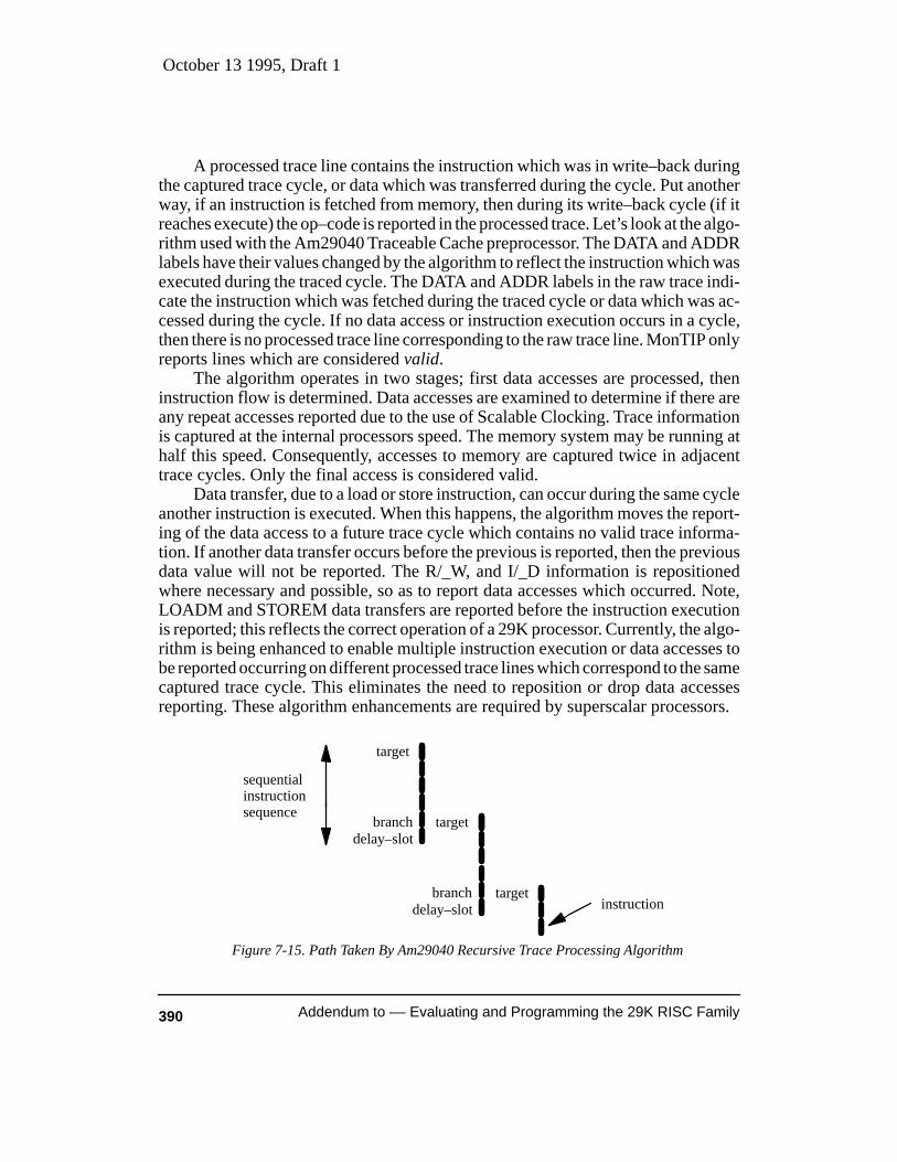
October 13 1995, Draft 1
390 Addendum to –– Evaluating and Programming the 29K RISC Family
A processed trace line contains the instruction which was in write–back duringthe captured trace cycle, or data which was transferred during the cycle. Put anotherway, if an instruction is fetched from memory, then during its write–back cycle (if itreaches execute) the op–code is reported in the processed trace. Let’s look at the algo-rithm used with the Am29040 Traceable Cache preprocessor. The DATA and ADDRlabels have their values changed by the algorithm to reflect the instruction which wasexecuted during the traced cycle. The DATA and ADDR labels in the raw trace indi-cate the instruction which was fetched during the traced cycle or data which was ac-cessed during the cycle. If no data access or instruction execution occurs in a cycle,then there is no processed trace line corresponding to the raw trace line. MonTIP onlyreports lines which are considered valid.
The algorithm operates in two stages; first data accesses are processed, theninstruction flow is determined. Data accesses are examined to determine if there areany repeat accesses reported due to the use of Scalable Clocking. Trace informationis captured at the internal processors speed. The memory system may be running athalf this speed. Consequently, accesses to memory are captured twice in adjacenttrace cycles. Only the final access is considered valid.
Data transfer, due to a load or store instruction, can occur during the same cycleanother instruction is executed. When this happens, the algorithm moves the report-ing of the data access to a future trace cycle which contains no valid trace informa-tion. If another data transfer occurs before the previous is reported, then the previousdata value will not be reported. The R/_W, and I/_D information is repositionedwhere necessary and possible, so as to report data accesses which occurred. Note,LOADM and STOREM data transfers are reported before the instruction executionis reported; this reflects the correct operation of a 29K processor. Currently, the algo-rithm is being enhanced to enable multiple instruction execution or data accesses tobe reported occurring on different processed trace lines which correspond to the samecaptured trace cycle. This eliminates the need to reposition or drop data accessesreporting. These algorithm enhancements are required by superscalar processors.
Figure 7-15. Path Taken By Am29040 Recursive Trace Processing Algorithm
target
branchdelay–slot
target
branchdelay–slot
targetinstruction
sequentialinstructionsequence

October 13 1995, Draft 1
391Chapter 7 Software Debugging
Data accesses which generate a cache hit are given the same treatment applied tomemory–resident data accesses. When a data transfer occurs, it will be reported in thenext available cycle (could be the current) which is not being used to report aninstruction’s execution or other valid data access. When the data cache is turned on, itwill not always be possible to report the value of the data transferred. The slave pro-cessor does not provide the cached data value, only the address.
For vector fetches, the vector fetch and the address of the first instruction as wellas the VECT status are reported on the same processed trace line.
The second stage of the algorithm is a little more complicated; it produces thecomplete address–flow for executed code. It currently only operates with 32–bitmemory accesses. Programs should not be traced when executing from 8–bitmemory devices. A recursive algorithm determines consecutive instruction execu-tion sequences, as shown on Figure 7-15. The algorithm starts with a branch instruc-tion and stops when it reaches a delay–slot instruction. Branch instructions initiatenew instruction sequences for the algorithm to recursively process.
Once the address flow is determined, a second recursive routine determines theinstructions which correspond to the address flow. Often these instructions arefetched from memory and can be found in the DATA field of a previous trace cycle.However, if the instruction is supplied by the instruction cache then XXXXXXXX isentered into the DATA column. If an address value lies in the loaded TEXT regionand the DATA column is marked XXXXXXXX, then the op–code is obtained fromthe loaded COFF file and placed in the DATA field.
MonTIP Commands
Strictly speaking, commands should be processed by the Debugger Front End(DFE), such as MonDFE. However, MonTIP has the capability of also processingcommands. The range of commands dealt with by MonTIP is greatly limited. EachDFE has a mechanism by which its command processing can be placed intransparent–mode. This causes commands to be passed to the TIP. With MonDFE,commands begining with the key word “tip” are passed to MonTIP. A number ofcommands have been added to MonTIP to support analyzer operation. By typing theMonDFE command “tip lahelp” a list of the commands will be displayed. TheMonTIP man–page describes the commands in more detail.
The MonTIP command “latadd label, width” is used to add a column to the tracelisting produced by MonTIP. An “latadd” should be used for each column in theprocessed trace listing. Acceptable values for “name” are defined by the labels whichappear in the raw trace listing. The only exception to this rule is for labelsSYMADDR and ASMDATA. These are pseudo labels derived from the raw labelsADDR and DATA respectively. The use of the SYMADDR label causes thehexadecimal address value to be replaced by an address symbol. For this to work the“lacoff file” command must be used to specify the file to be used during symbol tablelook–up. Addresses which are not found in the COFF file are presented in
October 13 1995, Draft 1
392 Addendum to –– Evaluating and Programming the 29K RISC Family
hexadecimal format. Use of the ASMDATA label indicates that the DATA labelinformation should be disassembled –– when the corresponding address is known tolie in a TEXT region.
The “latd start, end” command is used to display processed trace informationbased on stored lines. Processed line and raw line numbers are the same with regardto the processor status during the traced processor cycle, but only valid lines appear inthe processed trace listing. A valid line is one in which useful processor activity wasperformed. For valid lines, the ADDR, DATA, R/_W and I/_D labels are reevaluatedto correspond with the associated processor status value.
MonDFE Trace Access Commands
This section briefly describes MonDFE commands relating to displaying traceinformation. A complete list of MonDFE commands is obtained by entering thecommand “?”. MonDFE supports command files with the “zc file” command. It isuseful to place a list of “tip latadd SYMADD”–type commands in a command filesuch as la.rc. This enables the “zc la.rc” command to initialize MonTIP traceprocessing. The MonDFE command “ze file” can be used to record displayedinformation into a log file.
Before a trigger can occur, trigger conditions must be installed in the analyzer.The command “latrig term, label=pattern” can be used when setting trigger patternsin the logic analyzer. Specifying trigger logic and sequence control must be specifiedusing the analyzer window. Once the trigger has been established (and thePOD_040._D setup may be adequate) it is usually only necessary to use “latrig”commands such as “tip latrig a, ADDR=10004”. Trigger patterns can be entereddirectly using the analyzer window, this also requires the hexadecimal patten (ratherthan symbol) value be known. If the swaf program is used to build symbol tableinformation in Hewlett–Packard’s GPA format, it can be directly loaded into theanalyzer. This enables trigger labels to be set using symbols when directly using theanalyzer window.
The Analyzer can be triggered at each breakpoint by setting the break–addressto the illegal op–code vector address (vector 0). This technique is useful whenbreakpoints are implemented by temporarily replacing instructions with illegalop–code instructions. The MiniMON29K DebugCore uses this technique whenon–chip breakpoint registers are not available.
UDB Commands
UDB has been enhanced by CaseTools to support displaying trace informationin source format. This makes UDB a preferred tool for use with a logic analyzer.Additionally, UDB, like other non enhanced source level debuggers, can also be usedin transparent–mode. With transparent–mode operation, it is possible to issuecommands for MonTIP processing. Given that UDB supports source level tracing, itis unlikely that transparent–mode operation would be selected for use with UDB.

October 13 1995, Draft 1
393Chapter 7 Software Debugging
However, it is described here to aid users of other source level debuggers which onlyhave access to transparent–mode commands.
UDB is a window based debugger; however, command line processing issupported. When in the Main window or the Console window, a command linesequence begins with an <ESC> character. For example, to issue a “latadd” MonTIPcommand, use the command sequence “<ESC>ioctl tip latadd label”.
Alternatively, the “latadd label” command can be directly entered at theConsole window. If the console is not currently gathering input for an out–standingstandard input request (such as a scanf()), the keyboard input is sent to MonTIP forprocessing rather than the application or target operating system. It is useful to place alist of “ioctl tip latadd SYMADD”–type commands in a command file such as la.rc.The “<ESC>ioctl tip exec la.rc” command can then be used to process the MonTIPcommand file. An example la.rc file for use with UDB is shown below:
ioctl tip latclr;ioctl tip latadd LINE;ioctl tip latadd ADDR;ioctl tip latadd SYMADDR;ioctl tip latadd ASMDATA;ioctl tip latadd R/_W,6;ioctl tip latadd *STAT_,6;ioctl tip lamore 20;
The trace listing produced by commands such as “<ESC>ioctl latd 0, 20” willappear in the console window along with any other console output information suchas printf() output. It is also convenient to use UDB’s macro instruction capability tobind macros to buttons associated with the console frame. This allows user definedbuttons (left side of frame) to be simply clicked to issue the required MonTIPcommand. The macro instructions shown below can be placed in the udb.rc startupfile.
macro m=mcon –f –”echo” {lb6} ”{com}stty +echo\r”macro m=mcon –f –”trig” {lb7} ”{com}ioctl tip latrig a, ADDR=”macro m=mcon –f –”sync” {lb8} ”{com}ioctl tip lasync\r”macro m=mcon –f –”la.rc” {lb9} ”{com}exec la.rc\r”macro m=mcon –f –”coff” {lb10} ”{com}ioctl tip lacoff ”macro m=mcon –f –”help” {lb11} ”{com}ioctl tip lahelp\r”macro m=mcon –f –”latd” {lb12} ”{com}ioctl tip latd ”
Unprocessed analyzer trace was shown on Figure 7-14. The corresponding pro-cessed trace is shown on Figure 7-16. Trace information is presented in the consoleframe using UDB in a transparent–mode of operation. Although the Console windowis adequate, it is easier to study program execution from the enhanced trace window.
The enhanced trace window is shown on Figure 7-17. This window appearswhen the trace view–toolbar button (bottom right of window) is selected. The tracelisting window is formatted via the “trcol” command. This command, along with a
October 13 1995, Draft 1
394 Addendum to –– Evaluating and Programming the 29K RISC Family
number of other trace modifying commands, can be interactively entered at the UDBcommand line. However, it is much more typical to arrange for “trcol” commands tobe processed during UDB start–up. This is accomplished by entering a “trcol” com-mand sequence, such as the following example, into the udb.rc file.
trcol –d –w 8 ADDRtrcol –d –w 15 SYMtrcol –d –w 8 DATAtrcol –d –w 27 DASMtrcol –d –w 6 TYPEtrcol –d –w 6 STAT_
UDB fetches new trace information when the Fetch button is pressed. Thisbutton should be used whenever the analyzer has acquired new trace data. The Startand Stop buttons are provided for remote Running and Halting of the analyzer dataacquisition. This is equivalent to using the top–right–hand corner button on theanalyzer display. The Line button is used for displaying a desired line number ––entered via a dialog box. The Top button moves the current line (indicated by thecursor position) to the top of the display.
The Set button is particularly useful. The selected line is highlighted in red andthe raw analyzer display is adjusted as necessary to show the corresponding raw traceline. If any source–display windows are opened (in up–date mode rather than editmode), they are adjusted to show and highlight (in red) the corresponding C sourceline. The Loc button can be used to relocate the current highlighted line.
After a trace line has been selected and the Set button applied, the Next and Prevbuttons can be used to single step through source level trace. Using the Next button,all three displays (if in use) will be updated with the next line corresponding to therecorded source execution. If the shift key is held down while using the Next or Prevbutton, assembly level stepping rather than source level stepping is performed.
Trace column SYM is a synonym for column ADDR formatted symbolically.The address symbols are taken from the loaded symbol file. Hence the need to load aUDB symbol file produced by the mksym utility. The DASM column is a synonymfor DATA presented in disassembly format. When an instruction is supplied by theon–chip cache, XXXXXXXX is placed in the DATA column. However, the Xs willbe replaced with the actual instruction if an executable program has been loaded. Formore information on preparing the trace display see section 7.9.3.

October 13 1995, Draft 1
395Chapter 7 Software Debugging
Figure 7-16. UDB Console Window Showing Processed Trace Information

October 13 1995, Draft 1
396 Addendum to –– Evaluating and Programming the 29K RISC Family
Figure 7-17. UDB Trace Window Showing Processed Trace Information
October 13 1995, Draft 1
397Chapter 7 Software Debugging
7.9 Fusion3D TOOLS
Shortened development times and increased product complexity hasnecessitated the use of powerful software development tools. Unfortunatelyhowever, the higher processor speeds and on–chip integration provided by many ofthe newer embedded RISC processors has led to an increased cost associated withtraditional debug tools such as In–Circuit Emulators (ICE). Additionally, the rapidchanges occurring in the embedded processor market and the frequent introductionof processor variations has placed emphasis on the need for tool reusability.Reusable and low cost tools have a broad appeal among software designers.
The term Fusion3D refers to a Distributed Design and Debug environment. Thepurpose behind Fusion3D is to provide cost effective design and debug toolalternatives selectable from a range of compatible products. This is achieved bydistributing the primary tool functions. For example, traditionally a full–functionICE has been chosen as the primary debug tool. However, the overlay or substitutetarget memory provided by an ICE is alternatively available with a ROM emulator;the ICE’s tracing capability can be effectively achieved with a logic analyzer; andcontrolling program execution can be accomplished with a debug monitor andon–chip debug support hardware. The capabilities inherent in a full–function ICE aredistributed among the selected Fusion3D components. AMD has identified andworked with key Fusion3D partners to bring together the necessary components ofthe Fusion3D environment.
The Fusion3D approach is flexible. The scalable nature of Fusion3D enables thesoftware developer to construct a debug environment which is adequate for the taskto be undertaken, yet does not incur the high costs typically associated with afull–function ICE. At a later stage, if a project requires an additional debugcapability, the chosen tool combination can be enhanced.
Many of the tools provided by the Fusion3D program are useable with anymember of the 29K family or other processor family such as the X86. This helpsreduce the cost associated with tooling–up for a new project. For example, theHP16500B logic analyzer is widely used within the industry. Traditionally it has beenused by hardware development engineers. Extending its utility as a softwaredevelopment tool, useable across a wide range of processors, is very cost effective.
7.9.1 NetROM ROM Emulator
A ROM emulator is used to replace a system’s ROM or SRAM type memorydevices with substitute memory. Typically, ROM devices are removed from socketlocations on the target system and a cable used to connect the ROM emulator to thevacated sockets. The processor can read the emulated memory as if it were realROM. Occasionally there may be differences in memory access times due todifferent memory access wait states; but essentially the system runs as normal.
October 13 1995, Draft 1
398 Addendum to –– Evaluating and Programming the 29K RISC Family
ROM emulators always provide a second access port to the emulated memory.Via this second port, the contents of the memory can be read or written. This isgenerally accomplished by a host computer to which the ROM emulator is attached.The technique enables programs to be installed in system memory without the needto prepare (often termed burn) new ROM devices. During the process of developingand debugging software, modification of the program code frequently occurs.Consequently, an updated program must be reinstalled in the target system’smemory. The process of preparing new ROMs is slow, and a ROM emulator with afast computer link provides an alternative means of updating the system memory.
NetROM is a ROM emulator product provided by a Fusion29K tooldevelopment partner. It can emulate 8–bit, 16–bit or 32–bit wide memory devices asrequired. Depending on the width (number of bits) of the memory being emulated,between one and four cables are required to connect the NetROM to the target systemmemory. Up to 1M byte of memory can be emulated, depending on the pin layout ofthe memory devices in use. The 1M byte limitation does not restrict NetROM’s usefor developing programs which are larger than 1M byte –– this is achieved via theon–board UART. The UART is mapped into a location within the emulated memoryspace. The 29K processor can exchange data with the UART. The host computer canalso access the UART and hence exchange information with the 29K processor.
The MiniMON29K bundle contains a driver for the NetROM UART (oftenreferred to as a virtual UART). This enables the TIP program (MonTIP) running onthe host computer to communicate with the DebugCore software running on the 29Ktarget system. The method enables programs to be downloaded into the targetsystems DRAM memory. Typically, OS–boot, the DebugCore and support driversare placed in emulation memory; then, via MonTIP support, programs are loaded andexecuted out of the target system’s DRAM memory.
The NetROM equipment connects to the host computer via an Ethernetconnection. A NetROM can be used with an IBM PC compatible machine runningWindows; however, because of their Ethernet connection, they are much morefrequently used with networked Unix based systems. The Unix machine serving theNetROM will have an entry in (typically) its /etc/bootptab file, specifying the IP andEthernet addresses allocated to the NetROM. Also specified in the bootptab file is thethe path to the NetROM configuration file. An example bootptab file entry for aCMU type server is shown below. The actual NetROM configuration file is/tftpboot/netrom/startup2.bat. Note, for servers running in “secure” mode, the/tftpboot directory must be at the root of the path to the NetROM configuration file.The NetROM (client) Ethernet hardware address is given by the “:ha= ” field.
netrom2:hd=/tftpboot/netrom:bf=startup2.bat:sm=255.255.255.255:ht=1:ha=00402f008444:ip=163.181.22.60
When the host server connects to the NetROM client, the configuration file isdownloaded into the NetROM. A portion of the /tftpboot/netrom/startup2.bat is

October 13 1995, Draft 1
399Chapter 7 Software Debugging
shown below. The loadfile and loadpath variables are used to specify the defaultimage file to load into emulation memory. In the example below, the default imagefile is /tftpboot/netrom/target/sa29040.hex. The key parameters in the configurationfile should be arranged to describe the type of memory being emulated. The examplebelow shows four 27c020 memory devices combined to produce a 32–bit memorysystem. This will require four NetROM cables. It is possible (and common) toemulate only an 8–bit wide memory system.
;part of the startup2.bat NetROM configuration filesetenv host 163.181.22.9 ;server IP addresssetenv loadfile sa29040.hex ;29K program (image file)setenv loadpath /netrom/target ;path to 29k programsetenv romtype 27c020 ;ROM typesetenv romcount 4 ;number of ROMssetenv podorder 0:1:2:3 ;pod ordersetenv wordsize 32 ;memory width
A NetROM can support TELNET and direct TCP connections simultaneously.The MonTIP program forms a direct connection to the NetROM via the parameterinformation located in the udi_soc file (see section 7.5.6). An example udi_soc entryis shown below.
# udi_soc file entry to support NetROMnetrom2 AF_UNIX soc montip –t netrom –netaddr 163.181.22.60 –netport 1234
It is possible to have a TELNET session active with a NetROM while alsorunning MonTIP. Of course, the user controls the NetROM via a front–end debugtool such as UDB which directs the operation of MonTIP via the UDI interface. Froma window running the TELNET command “telnet netrom2” (for example), the“newimage” NetROM command can be used to download a file (usually the default)into emulation memory. The sa29040.hex image file contains OS–boot, theDebugCore, and support driver code for an SA29040 evaluation board. Onceinstalled it enables DebugCore messages to be exchanged between the 29K targetand the host computer running MonTIP.
A software reset can be performed by issuing a reset command from UDB.Normally the DebugCore is successfully running and will perform the reset. Underextreme conditions the DebugCore may no longer be in control of the 29K processor.In this case a hardware reset can be performed. This requires that the 29K reset pin beasserted. From the TELNET session this is accomplished via the “tgtreset”command. The technique requires that a reset wire be used to connect the reset outputpin on the back of the NetROM (marked R) to a connection post on the target system.The connection post must be wired to the processor reset pin. For this reason, it is bestto incorporate a reset connection post on each 29K target system for use by theNetROM.
Once a NetROM has been added to a network, a TELNET connection can beused to confirm its correct installation. After issuing a “newimage” command, and
October 13 1995, Draft 1
400 Addendum to –– Evaluating and Programming the 29K RISC Family
possibly a “tgtrest” command, the 29K target system is ready for operation. Thechosen debug tool (UDB, GDB, etc.) can then be invoked and used to examine,modify and control the target 29K processor in the normal way. Once correctinstallation has been confirmed, there is no need to first establish a TELENTconnection before initiating normal program debug. All that is necessary is to startexecution of the chosen debugger.
The NetROM driver (for the 29K side of the virtual UART) that is built into theimage file, typically operates in poll–mode. This refers to the 29K processor onoccasion polling the UART to determine if it is receiving a message from MonTIP.The image file can be built with an interrupt–mode driver. This enables MonTIP tointerrupt the 29K at any time (if interrupts are enabled) when it wishes to send amessage (such as halt) to the DebugCore. To enable operation of this technique, aninterrupt wire must be used to connect the interrupt output pin on the back of theNetROM to an interrupt input post on the 29K system. Once again, the post should beincorporated into any design which wishes to make sue of a NetROM.
7.9.2 HP16500B Logic Analyzer
Network Installation
The use of logic analyzers for tracing program execution was previouslypresented in section 7.8. This section briefly deals with the details of configuring thelogic analyzer’s operation for use in the Fusion3D environment. A high speedconnection to the analyzer is achieved via the optional Ethernet link. This requiresthat the analyzer be allocated a unique IP address. Using the analyzer’scommunications set–up window, the IP address is recorded for future use. With Unixnetworks, the IP address and chosen name are entered into the network database file/etc/hosts. The following example allocates an IP address for an analyzer called“hpla”.
#entries in /etc/hosts file allocating IP addresses163.181.22.117 hpla # logic analyzer163.181.22.121 ginger # X–terminal
The analyzer connection can be confirmed by establishing a telnet connection.This is accomplished with a “telnet hpla 5025” command. Port number 5025 enablesaccess to the analyzer command parser. Commands can then be directly issued to theanalyzer. One very useful command: “xwin on, ’163.181.22.121:0.0’”, establishes aremote window interface to the analyzer. The example command shown causes ananalyzer front panel interface to be presented on the display determined by the IPaddress 163.181.22.121. Checking the example /etc/hosts file, it appears to be anX–terminal known to the network by the name ginger. It is important that the X serverallow the analyzer to make connection to the server. The “xhost + hpla” commandcan be used to add hpla to the list of machines that are allowed to make connection to
UDI session_id
executable UDI session_id
October 13 1995, Draft 1
401Chapter 7 Software Debugging
the X server. To obtain the name of your terminal’s display, print the environmentvariable DISPLAY as shown below.
echo $DISPLAY #Unix shell commandginger:0.0 #response
It is important for the successful operation of MonTIP that the environmentvariable DISPLAY be correctly initialized. Note that some HP workstations set thevariable to the value “local:0.0”, this does not create any difficulty for MonTIP.UDI Installation
The udi_soc file (for Unix based systems) must contain an entry forestablishing, via UDI, the MonTIP to analyzer connection. The MonTIP option “–laname” is provided for this purpose. The example below shows a udi_soc entry for asession identified by the name “trace”. Note that the udi_soc file format wasdescribed in detail in section 7.5.6. If a logic analyzer were being used alone, theexample udi_soc entry would be adequate. However, a NetROM is typicallycombined with an analyzer. In this case the two entries shown below would becombined to produce a single entry with a unique session identifier.
# udi_soc file entry to support logic analyzer1trace AF_UNIX soc montip –la hplarom AF_UNIX soc montip –t netrom –netaddr 163.181.22.60 –netport 1234
When using the UDB source level debugger to control a logic analyzer, amktarget command must be placed in the udb.rc start–up command file. Asexplained in section 7.7, a GIO process, controlled by UDB, uses the assignedmktarget parameters to connect to a 29K target (in this case via MonTIP). Anexample udb.rc entry is shown below.
# udb.rc, UDB startup command file#driver args (GIO ID, GIO executable, exec. flags, udi_soc session ID)#mktarget name id type driver (args....)mktarget LA 1 29040 dr_gio 0 ios_udi –be trace
Note that normally the GIO and UDB processes determine the endian of the 29Ktarget via examining the processor’s CFG special register. When an analyzer is usedalone, there is no connection to the 29K processor and the CFG register can not beaccessed. This necessitates that the mktarget command specify the target endian.The “–be” switch is used in the example to select big–endian operation. The “–le”switch is available for selecting little–endian. The following section 7.9.3 describeshow user defined buttons can be used to issue mktarget commands.Accessing the Analyzer File System
It is very convenient to be able to drive the logic analyzer remotely from, say, theX–terminal on your desk. Note that a colour monitor is required to achieve full

October 13 1995, Draft 1
402 Addendum to –– Evaluating and Programming the 29K RISC Family
control of the analyzer. As described above, remote control of the analyzer is enabledvia the “xwin on” command. When remote control of the analyzer is no longerrequired, the command “xwin off”, entered via the telnet connection to the analyzer,discontinues the remote display. Connection to the analyzer command parser isbroken when the TELNET session is terminated.
Only one user can be in control of the analyzer at any time. This means theanalyzer can not be driven from the front panel when a remote window is active.When MonTIP controls the analyzer, it requests a remote window be presented on theMonTIP host computer (actually, the DISPLAY variable identifies the screen).Consequently, it is not possible for another user to establish a second remote windowconnection. However, it is possible to simultaneously have an FTP connection activewhen remotely controlling the analyzer. The example command sequence belowdemonstrates how this is achieved.
1% ftp hpla #Unix shell commandConnected to hpla.220 HP16500B V01.00 FUSION FTP server (Version 3.3) ready.Name (hpla:danm): data230 User DATA logged in.ftp> cd system/disk/hard/amd/danm200 Remote Directory changed to ”/system/disk/hard/amd/danm”.ftp>
When entering a login name, the identifier “data” was used in the aboveexample. This enables read access to files located on the analyzer disk system.Entering the identifier “control” enables read–write access to the file system.However, logging in as “control” is not permitted if another user is identified asalready controlling the analyzer. Files can be transferred from/to the analyzer usingthe FTP commands get/put; remember you may have to first use the binary commandto enable transfer of binary data files.Triggering the Analyzer for Trace Capture
The HP16500B logic analyzer is equipped with a very sophisticated triggeringcapability. Hence, debuggers controlling the logic analyzer tend to rely on theanalyzer’s triggering logic. When using the PI–Am29040 preprocessor, thePOD_040 configuration file prepares the analyzer for triggering on access to thememory location described by analyzer trigger term A. This may, or may not, beadequate for your triggering requirements. All changes to trigger logic must beentered using the logic analyzer front panel display (remotely if desired). If using thePOD_040 file, all that is necessary is to supply the trigger address in the ADDR fieldof term A. Of course the address must be entered in hexadecimal format unless asymbol file has been loaded into the analyzer.
When on–chip caches are used, instruction and data accesses may not alwaysappear on the processor bus. This complicates the task of triggering the analyzer. It isalso not possibly to simply use the ADDR field of term A when a microcontroller is
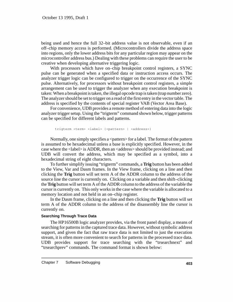
October 13 1995, Draft 1
403Chapter 7 Software Debugging
being used and hence the full 32–bit address value is not observable, even if anoff–chip memory access is performed. (Microcontrollers divide the address spaceinto regions, only the lower address bits for any particular region may appear on themicrocontroller address bus.) Dealing with these problems can require the user to becreative when developing alternative triggering logic.
With processors which have on–chip breakpoint control registers, a SYNCpulse can be generated when a specified data or instruction access occurs. Theanalyzer trigger logic can be configured to trigger on the occurrence of the SYNCpulse. Alternatively, for processors without breakpoint control registers, a simplearrangement can be used to trigger the analyzer when any execution breakpoint istaken: When a breakpoint is taken, the illegal opcode trap is taken (trap number zero).The analyzer should be set to trigger on a read of the first entry in the vector table. Theaddress is specified by the contents of special register VAB (Vector Area Base).
For convenience, UDB provides a remote method of entering data into the logicanalyzer trigger setup. Using the “trigterm” command shown below, trigger patternscan be specified for different labels and patterns.
trigterm <term> <label> {<pattern> | <address>}
Normally, one simply specifies a <pattern> for a label. The format of the patternis assumed to be hexadecimal unless a base is explicitly specified. However, in thecase where the <label> is ADDR, then an <address> should be provided instead; andUDB will convert the address, which may be specified as a symbol, into ahexadecimal string of eight characters.
To further simplify issuing “trigterm” commands, a Trig button has been addedto the View, Var and Dasm frames. In the View frame, clicking on a line and thenclicking the Trig button will set term A of the ADDR column to the address of thesource line the cursor is currently on. Clicking on a variable and then shift–clickingthe Trig button will set term A of the ADDR column to the address of the variable thecursor is currently on. This only works in the case where the variable is allocated to amemory location and not held in an on–chip register.
In the Dasm frame, clicking on a line and then clicking the Trig button will setterm A of the ADDR column to the address of the disassembly line the cursor iscurrently on.
Searching Through Trace Data
The HP16500B logic analyzer provides, via the front panel display, a means ofsearching for patterns in the captured trace data. However, without symbolic addresssupport, and given the fact that raw trace data is not limited to just the executionstream, it is often more convenient to search for patterns in the processed trace data.UDB provides support for trace searching with the “trsearchnext” and“trsearchprev” commands. The command format is shown below:

October 13 1995, Draft 1
404 Addendum to –– Evaluating and Programming the 29K RISC Family
trsearchnext [<label> {<pattern> | <address>}]trsearchprev [<label> {<pattern> | <address>}]
Normally, one specifies a search <pattern> for a selected <label>. However, inthe case where the <label> is ADDR, then an <address> should be provided instead.In such case, UDB will convert the address, which may be specified as a symbol, intoa hexadecimal string of eight characters.
After a <label> and <pattern> have been specified, UDB remembers them toallow for further searching without having to specify the <label> and <pattern>again. In particular, the Next and Prev keys in the trace frame have been overloaded,such that Ctrl–Shift–Clicking them will issue these commands with no parameters.
UDB supports the binding of buttons to macro commands. This is a convenientmeans of issuing “trsearchnext” commands. The following udb.rc commandsequence assigns buttons to the macro table associated with the Trace frame. Notethat user programmed buttons should be restricted to the left hand side of the window.The example command creates two buttons. The next button can be used initiate a“trsearchnext” command. Because the command–string does not finish with a “\r”character, the user can enter the <pattern> from the command line interface.
# macro table button position command# –––––– –––– ––––– ––––––––––––––––– . . .macro m=mtrace –f “next” {lb1} “{com}trsearchnext ADDR ”macro m=mtrace –f “prev” {lb2} “{com}trsearchprev ADDR ”
7.9.3 Selecting Trace Signals
In section 7.8 under the headings MonTIP Commands and UDB Commands,techniques for formatting the trace display were presented. Groups of processor sig-nals, such as the address bus, are grouped together and assigned labels. The user canalways rely on the following four labels being available for display: ADDR, DATA,LINE, TYPE. Different 29K family members, and different system configurations,will provide a number of other useful labels, such as R/_W. Given the limited size ofthe trace display, it is necessary to limit the number of trace labels.
Depending on the source level debugger selected, or if MonTIP is being used toformat the trace display, there may be synonyms for the main trace labels. For exam-ple: ADDR is also known as SYM by UDB, and as SYMADDR by MonTIP. Thesealternatives to ADDR, enable the traced address values to be presented symbolically,even if the logic analyzer is configured to display them in, say, hexadecimal. An alter-native implementation would have been to support a format parameter for control-ling the displaying of selected labels. But, so far, this has not been the route taken bysource level debugger implementors. Note that if the SYM label is selected, it is nec-essary to load a UDB symbol file. This file is produced by the mksym utility.
The DASM column is a synonym for DATA presented in disassembly format.The trace processing algorithms used with the Am29040 processor place
October 13 1995, Draft 1
405Chapter 7 Software Debugging
XXXXXXXX in the DATA column when an instruction is supplied by the on–chipcache. However, the Xs will be replaced with the actual instruction if an executableprogram has been loaded. For replacement to be successful, the Am29040 targetprocessor must be executing with physical addressing or with a one–to–one virtual tophysical address translation scheme. This is because the Am29040 slave processorproduces physical address values. The virtual addresses inherent in the loadedprogram must correspond to the physical addresses appearing on the processoraddress bus. The Am29460 slave processor produces virtual addresses, but this doesnot entirely solve the problems created by the use of address translation. I will saymore about this in section 7.9.5.
As explained in section 7.8, the trace listing frame is formatted with the “trcol”command. This is accomplished by entering a “trcol” command sequence, such asthe following example, into the start–up udb.rc file. The “–w” parameter specifies themaximum display width (in characters) for a label. The udb.rc file is accessed fromthe current working directory or from your home directory.
trcol –d –w 8 ADDR #general trace labelstrcol –d –w 15 SYM #symbolic adresstrcol –d –w 8 DATA #data bus valuetrcol –d –w 27 DASM #disassembled DATA labeltrcol –d –w 6 TYPE #type of operation
trcol –d –w 6 STAT_ #additional Am29040 trace label
Displaying a large number of labels will require a wide trace frame. It is useful toinitially define a large View frame, which can later be switched to displaying trace.When UDB is invoked, a fixed sized null frame is randomly positioned on the dis-play. Using the following udb.rc command sequence, the null frame can be replacedwith a user specified window size positioned at the top left hand corner of the screen.After creating the View frame, the null window is deleted.
#create X Y rows columns type udb.rc command wcreate 0 0 –g 24 90 view #create new View framewdelete 0 #delete original null window
UDB supports the binding of buttons to macro commands. This is a convenientmeans of issuing mktarget commands, rather than hard–wiring them into udb.rc.This simplifies the task of selecting from a number of different mktarget options.Given that the View frame is established during UDB start–up (as described above),the following udb.rc commands assign buttons to the macro table associated with theView frame. Note that user programmed buttons should be restricted to the left handside of the window. The example command sequence creates two buttons. The buttonmarked “LA” can be used to establish a connection to a logic analyzer. The “view –u”command causes a source frame to be invoked. If the 29K program counter iscurrently not in source but in disassembly, the disassembly view will be invoked.

October 13 1995, Draft 1
406 Addendum to –– Evaluating and Programming the 29K RISC Family
# macro table button position command# –––––– –––– ––––– ––––––––––––––––– . . .macro m=mview –f “iss” {lb1} “mktarget ISS 1 29040 dr_gio 0 ios_udi simulator; view –u\r”macro m=mview –f “LA” {lb2} “mktarget LA 1 29040 dr_gio 0 ios_udi –be trace; view –u\r”
7.9.4 Corelis PI–Am29040 Preprocessor
A logic analyzer preprocessor simplifies the connection of the analyzer to thetarget system. The principles behind its operation were discussed in section 7.8. Thissection briefly deals with the operating details encountered with the Am29040 pre-processor. To prepare the preprocessor based system, a number of steps must be take:
1. The PI–Am29040 Preprocessor hardware unit replaces the Am29040processor in the target system. The preprocessor contains two Am29040processors, one operating in master mode, the other in slave mode. Earlierversion of the preprocessor required that certain pins such as MEMCLK(H–14) on the slave processor be removed. Later versions do not require pinremoval. There is a jumper option for removing the slave MEMCLK signal ifit is configured as an output. If MEMCLK is configured as an input, the slaveand master MEMCLKs must be tied together. Because of the high speedoperation of Am29040 based systems, the use of PGA socket extendersshould be limited as they add to signal propagation delays. It is oftendesirable to add extenders to the preprocessor connection pins to protect themfrom damage. If a pin gets broken, it is less expensive to replace a socket thanto replace the preprocessor. Zero ohm resistors have been incorporated inseries with a number of signal pins, such as MEMCLK and INCLK.Impedance matching, and hence better signal conditioning, can be achievedby replacing these resistors with an appropriate value resistor.
2. If HP16550A logic analyzer cards are being used with the HP16500B system,then two cards should be wired together in accordance with the HPInstallation Manual. Two analyzer cards provide a total of 12 trace pods.Assuming the cards are located in slots D and E, pod E1 (slot E – master)should be connected to position J1 on the preprocessor. Pod E2 to position J2,and so on. Pods D1–D3 should be connected to J7–J9 (see Table 7-5). Theanalyzer configuration file POD_040._D will format the analyzer cards forthis configuration. (The ._D file name postfix, is because the master analyzercard is located in card cage slot D.) The POD_040 configuration file isavailable from AMD or Corelis. It is important to obtain a copy of theconfiguration file, as it is much too time consuming to reassign thepod–to–label mapping by hand.
October 13 1995, Draft 1
407Chapter 7 Software Debugging
Table 7-5. PI–Am29040 Logic Analyzer Pod Assignment
Analyzer podPreprocessor connector Analyzer pod
expander 1J1 master 1
HP16550A HP16555A
expander 2J2 master 2expander 3J3 master 3expander 4J4 master 4master 1J5 master 5master 2J6 master 6
J7 expander 1master 3J8 expander 2
PI–Am29040
master 4J9 expander 3
pods forcapturingclock signals
3. If the more expensive HP16555A logic analyzer cards are selected, two cardsare still required. Once again they should be wired together in accordancewith the HP Installation Manual. Note that even if a pair of cards arepurchased together, they may not be interconnected in accordance with HP’smanual recommendations. Two HP16555A analyzer cards provide a total of6 trace pods. Assuming the cards are located in slots A and B, pod B1 (slot B –expander) should be connected to position J1 on the preprocessor. Pod B2 toposition J2, and so on. Pods A1–A2 should be connected to J5–J6, and podsA3–A4 to connections J8–J9 (skipping J7), see Table 7-5. The analyzerconfiguration file POD_040._A will format the analyzer cards for thisconfiguration. Note that the configuration file required for HP16555A cards,although the same name, is not the same file required to configure HP16550Acards. The reason B–pods are allocated before the A–pods is because the cardin the B slot is wired as an expander card and all clock signals must beacquired by the master card in slot A. The configuration file specifies thattrace signals are captured on MEMCLK signal edges, and MEMCLK isprovided on connector J5.
4. If the 29K target system is operating with 1x clocking, then the master clockshould be configured to acquire trace data on the rising edge of MEMCLK. If2x Scalable Clocking is being used, the master clock should acquire tracedata on both the rising and falling edge of MEMCLK. The appropriateselection can be made from the analyzer control panel (remotely if desired).With newer versions of the preprocessor (those that provide access to theprocessor’s DIV2 pin), the MonTIP software warns the user that the wrongedge–selection has been made.
5. There is no need to install the Corelis preprocessor support software suppliedwith the PI–AM29040. However, if it is installed then is will be possible to
October 13 1995, Draft 1
408 Addendum to –– Evaluating and Programming the 29K RISC Family
present disassembled instructions on the analyzer display. Using the Corelissoftware, trace label DATA can be displayed in Invasm (inverse assembler)format without resulting in any conflicts with MonTIP’s access to DATA.There is no advantage to using the disassemby software, as the analyzerdisplay shows instructions which are fetched but not necessarily executed.
6. There are a number of limitations imposed by the Am29040 Traceable Cachearchitecture. These where previously discussed in section 7.8 under theheading Processing Trace Information. Very briefly, the complete instructionflow is reported: Labels, DATA, ADDR, R/_W and I/_D have their valuesmanipulated to report the instruction which was executed during the tracedcycle.
7. The trace data processing algorithms built into MonTIP need to know theendian–ness of the 29K target processor. When connection to the analyzer isestablished, a window displaying the analyzer control panel will appear.MonTIP prints a message in this window indicating the endian–ness of thetarget processor. If the endian–ness is unknown, MonTIP will continueoperating; but sub word–sized data accesses will only be partially processed.To fully process data accesses, the “Analyzer 1:Name” field provided underthe logic analyzer “Configuration” window should be set to AM29040B orAM29040L, respectively for big or little endian operation.
8. The MonTIP algorithms are currently restricted to operating with systemswhich fetch instructions from 32–bit memory. This does not necessitate that32–bit ROM emulation be used with NetROM. If application programs areloaded and execute from 32–bit memory, they can be successfully traced.However, if interrupt handlers or other support code is run from 8–bitmemory, tracing will not be possible.
9. can’t reduce capture rules
7.9.5 Corelis PI–Am29460 Preprocessor
A logic analyzer preprocessor simplifies the connection of the analyzer to thetarget system. The principles behind its operation were discussed in section 7.8. Thissection briefly deals with the operating details encountered with the Am29460preprocessor. For those simply interesting in getting their preprocessor working, andnot at this stage needing to understand the background behind its operation, proceedto the section with the subheading PI–Am29460 Setup and Limitation.
The Traceable Cache information provided by the Am29040 slave processor issynchronous with program execution. If this approach were taken with the Am29460microcontroller, the superscalar execution capability would necessitate very highspeed trace reporting. To reduce the slave processor’s information bandwidth

October 13 1995, Draft 1
409Chapter 7 Software Debugging
requirements, the Am29460 does not synchronize trace reporting with programexecution. The Am29460 trace information is compressed, relative to the Am29040trace data, and held in an output queue before being transferred off–chip.PI–Am29460 Preprocessor Operation
The main processor operation is driven by the PCI INCLK signal pin. However,for data capturing purposes, the logic analyzer master clock is the slave trace clock(TRACECLK). It runs at half the internal clock speed. Note that the internal clock(not available on a pin) runs at 2x, 3x or 4x the INCLK speed. With 2x clocking andsingle–cycle MCU transfer rates, the MCU access speed would equal theTRACECLK speed. With 2x, or higher scaling ratios, the PCI and MCU data transferrates can not exceed the frequency of TRACECLK. This enables TRACECLK to beused as the master clock by the logic analyzer.
The analyzer captures signal values when the master clock is active. There alsohas to be at least one of the following conditions: valid trace information, a valid PCIaccess, a valid MCU access. PCI accesses are first captured by the analyzer slaveclock. The PCI INCLK is used to capture logic analyzer slave information. Analyzerslave signals are transferred into the logic analyzer trace buffer on the next masterclock signal. If more than one slave value is captured before the next master clock,then only the most recent slave values are stored in the analyzer trace buffer. For thisreason it is important that the master clock operate at a higher frequency than theslave clock.
The HP16500B analyzer only supports one slave clock. For this reason, MCUaccess are latched and held until the next master clock edge; during which any PCIaccess captured by the slave clock are recorded by the analyzer, see Figure 7-18. It isimpossible for two MCU accesses to occur before the next TRACECLK, even ifanother agent uses the PCI to access an MCU. Anyway, the trace processingalgorithms are only interested in MCU accesses initiated by the processor, not thePCI. The preprocessor and its supporting software are not intended to form a generalpurpose PCI probe.
Logic analyzer trace buffer
MCU latched signals PCI signals
Master clockTRACECLK(delayed)
Slave clockINCLK (and other
conditions)_STROBE
CAS, RAS
Figure 7-18. PI–Am29460 Preprocessor Trace Capture Scheme
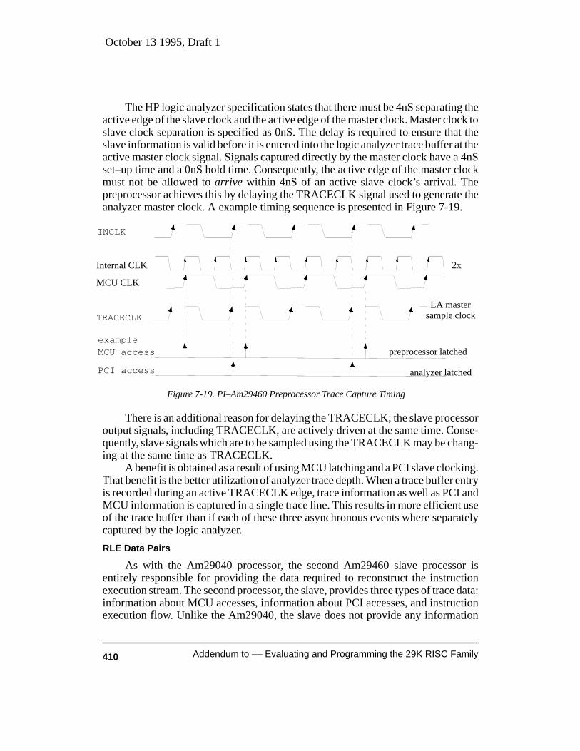
October 13 1995, Draft 1
410 Addendum to –– Evaluating and Programming the 29K RISC Family
The HP logic analyzer specification states that there must be 4nS separating theactive edge of the slave clock and the active edge of the master clock. Master clock toslave clock separation is specified as 0nS. The delay is required to ensure that theslave information is valid before it is entered into the logic analyzer trace buffer at theactive master clock signal. Signals captured directly by the master clock have a 4nSset–up time and a 0nS hold time. Consequently, the active edge of the master clockmust not be allowed to arrive within 4nS of an active slave clock’s arrival. Thepreprocessor achieves this by delaying the TRACECLK signal used to generate theanalyzer master clock. A example timing sequence is presented in Figure 7-19.
INCLK
MCU access
PCI access analyzer latched
preprocessor latched
Internal CLK 2x
TRACECLKLA master
sample clock
MCU CLK
example
Figure 7-19. PI–Am29460 Preprocessor Trace Capture Timing
There is an additional reason for delaying the TRACECLK; the slave processoroutput signals, including TRACECLK, are actively driven at the same time. Conse-quently, slave signals which are to be sampled using the TRACECLK may be chang-ing at the same time as TRACECLK.
A benefit is obtained as a result of using MCU latching and a PCI slave clocking.That benefit is the better utilization of analyzer trace depth. When a trace buffer entryis recorded during an active TRACECLK edge, trace information as well as PCI andMCU information is captured in a single trace line. This results in more efficient useof the trace buffer than if each of these three asynchronous events where separatelycaptured by the logic analyzer.
RLE Data Pairs
As with the Am29040 processor, the second Am29460 slave processor isentirely responsible for providing the data required to reconstruct the instructionexecution stream. The second processor, the slave, provides three types of trace data:information about MCU accesses, information about PCI accesses, and instructionexecution flow. Unlike the Am29040, the slave does not provide any information

October 13 1995, Draft 1
411Chapter 7 Software Debugging
about data cache hit activity. Data about Instruction flow is provided in the form ofaddress–length pairs, known as Run Length Encoding (RLE).
The Am29040 slave processors does not need to provide access typeinformation about data accesses, as they can be fully observed by monitoring themain processors data busses. However, many of the bus signals available with a2–bus processors are not available with a 29K microcontroller. For example, the I/_Dpin is not available. This means when a memory read access is performed, it is notpossible to determine if data or an instruction is being fetched. With the Am29460processor, the slave provides this type of information. This explains why the slaveprovides trace data for both MCU and PCI accesses performed by the masterprocessor.
Before describing the RLE technique in more detail, we must first remindourselves of the speculative execution nature of the Am29460 processor. Asexplained in section 1.7, instructions are fetched and speculatively executed.However, instruction are not truly consider to have executed until they have beenretired. This introduce the notion of a Retire Program Counter (R–PC). At any time,instructions who’s addresses are ahead of the R–PC may be held in the reorder bufferwaiting for potential retirement. Special register PC1 contains the address of theinstruction currently in execution. Because the processor supports precise interrupts,the PC1 register can never get ahead of the R–PC address. When a trap or interrupt istaken, the R–PC value will appear in register PC1 or PC0 (decode address)depending on the stage at which the processor pipeline is interrupted.
Each RLE (TRACEADDR, TRACERUN) data pair specifies thatTRACERUN instructions, starting from the current R–PC, have been retired, andsubsequent retirement is to continue from an R–PC value of TRACEADDR. ATRACERUN value of zero is permitted; it is used to redirect trace flow withoutrecording any instruction execution (retirement). In such case a TRACEADDRvalue change accompanies the TRACERUN zero value. A value of zero is also usedto indicate that no instructions are available for retiring. In such case theTRACEADDR value does not change. An example RLE trace sequence is shown onFigure 7-20.
An RLE data pair can be output by the slave processor during the rising edge ofeach TRACECLK. The RLE data is not provided directly by the reorder buffer, butby a buffer queue which receives its input from the reorder buffer, see Figure 7-21.This is necessary as very short run lengths produce RLE data at a rate faster than theTRACECLK can report them. Using a queue reduces the need to stop instructionretirement until the RLE data has been presented on the slave output pins. However,the queue is limited in size and consequently, under rare circumstances, it canbecome full. This results in the master processor postponing instruction retirementuntil a queue entry is available. Without this throttling back approach, uninterruptedreporting of instruction flow could not be guaranteed.

October 13 1995, Draft 1
412 Addendum to –– Evaluating and Programming the 29K RISC Family
Figure 7-20. Slave Data Supporting Am29460 Traceable Cache
sequentialinstructionretirement
TRACEADDR
TRACERUN
TRACEADDR
TRACEADDR
branch instructiondelay–slot
t arget instructionTRACEADDR
address–length pair
program flow
consecutive group ofretired instructions oflength TRACERUN
Figure 7-21. RLE Output Queue From Reorder Buffer
TRACERUN
. . .RLE entryRLE entryRLE entry
TRACEADDR
Reorder buffer retirement
Slave processor output pinsclocked at TRACECLK speed
Run–Length Encodingoutput queue
Given that the TRACECLK runs at half the internal speed of the processor, asmany as 8 instructions could be retired at each TRACECLK interval. However, as ameans of reducing RLE queue entries, an entry is not placed in the queue if the currentsequence of instructions being retired does not contain a branch instruction. In suchcase, the TRACRUN is allowed to accumulate to a maximum of 31, the largest valuewhich can be reported on the 5–pins allocated to TRACERUN. Research (see section1.7.4, [Johnson 1991]) has shown that instruction sequences typically contain five orsix instructions before branching. This would indicate that TRACERUN values near

October 13 1995, Draft 1
413Chapter 7 Software Debugging
31 will not be a frequent occurrence, and values in the range five or six are to beexpected.PI–Am29460 Setup and Limitations
As with the PI–Am29040 preprocessor, a number of restrictions andpreparation steps apply when using the PI–Am29460 preprocessor:1. The trace processing algorithm places the value X_SLAVE_ in the DATA
column for all instruction accesses. It is necessary to have access to the COFFfile(s) for the loaded program to ensure the X_SLAVE_ value is replaced withthe actual 29K instruction executed. Debuggers such as UDB can retainmultiple COFF file images at the same time. This enables simultaneoustracing of application space and operating system space (say, interrupthandlers).
2. Considering MCU performed memory accesses, only data accesses arereported. Data transfer is shown at the time it appears on the system busses;which, for data stores, may be several cycles after the corresponding STOREinstruction.
Two bus 29K processors have OPT pins and lower (A1–A0) address pinswhich indicate the size and alignment of the object currently being accessed.The Am29460 microcontroller does not have these pins. Consequently it isnot possible to determine the alignment and size for reads of sub word–sizedobjects. Fortunately, the microcontroller has four byte enable pins which areused for data writes. This enables the alignment and size of objects which arewritten to be determined, and improves the trace reporting for data writes.
Only MCU accesses performed on behalf of the Am29460 processor arereported. Accesses initiated by another processor via the PCI interface willnot appear in the trace.
3. Considering accesses to the PCI bus, as with MCU accesses, only datatransfers are reported. By monitoring the PCI command provided during theaddress–phase of a PCI access, it is possible to determine the object size forsub word–sized objects.
4. The PI–Am29460 preprocessor does not reconstruct 32–bit MCU addresses.This can complicate logic analyzer triggering. One solution is to use theon–chip breakpoint control registers to generate a _SYNC pulse which isthen used to trigger the analyzer. The UDB debugger has a convenient userinterface for specifying breakpoint control register operation. Unfortunately,however, breakpoint control registers are a limited resource, and they are alsoused to control program execution.
5. Unlike a scalar processor, processed trace lines with the Am29460, indicatemultiple instruction execution per trace line. The number of instructions
October 13 1995, Draft 1
414 Addendum to –– Evaluating and Programming the 29K RISC Family
reported executed by a trace line has less to do with the instruction retirementrate and more to do with the run–length between branch instructions. Whenan MCU or PCI access occurs at the same time as RLE reporting, theprocessed trace indicates all activity on the same processed trace line.
6. The trace data processing algorithms built into MonTIP need to know theendian–ness of the 29K target processor. When connection to the analyzer isestablished, a window displaying the analyzer control panel will appear.MonTIP prints a message in this window indicating the endian–ness of thetarget processor. If the endian–ness is unknown, MonTIP will continueoperating; but sub word–sized data accesses will only be partially processed.To fully process data accesses the “Analyzer 1:Name” field provided underthe logic analyzer “Configuration” window should be set to AM29460B orAM29460L, respectively for big or little endian operation.
7. If HP16550A logic analyzer cards are being used with the HP16500B system,then two cards should be wired together in accordance with the HPInstallation Manual. Two analyzer cards provide a total of 12 trace pods. Ifthe more expensive HP16555A logic analyzer cards are selected, three cardsare required. Once again they should be wired together in accordance with theHP Installation Manual. Note that even if cards are purchased together, theymay not be interconnected in accordance with HP’s manualrecommendations.
Table 7-6 shows the assignment of analyzer pods to preprocessor connectors.The analyzer configuration file POD_460._A will format the analyzer cardsfor this configuration. (The ._A file name postfix, is because the masteranalyzer card is located in card cage slot A.) The POD_460 configuration fileis available from AMD or Corelis. It is important to obtain a copy of theconfiguration file, as it is much too time consuming to reassign thepod–to–label mapping by hand.
Note that the configuration file required for HP16555A cards, although thesame name, is not the same file required to configure HP16550A cards.
8. A logic analyzer, controlled by UDB, may be attached to a 29K target systemwhich is not under UDB control. This is the case where a logic analyzer isused alone, without the utilization of, say, a NetROM. It is also the case whenpreviously captured trace data is reexamined. To enable 32–bit addressreconstruction, the algorithms built into MonTIP need to know theprocessor’s bank profile register (BPR) settings. MonTIP normallyaccomplishes this by accessing the DebugCore each time trace data isfetched. When no DebugCore is present, MonTIP is provided the BPR valuesfrom the udb.rc initialization file.

October 13 1995, Draft 1
415Chapter 7 Software Debugging
Table 7-6. PI–Am29460 Logic Analyzer Pod Assignment
Analyzer podPreprocessor connector Analyzer pod
master 1J1 master 1
HP16550A HP16555A
master 2J2 master 2master 3J3 master 3master 4J4 master 4
first expander 1J5 master 5first expander 2J6 master 6first expander 3J7 expander 1first expander 4J8 expander 2
PI–Am29460
second expander 1J9 expander 3second expander 2J10 expander 4second expander 3J11 expander 5second expander 4J12 expander 6
pods forcapturingclock signals
The BPR registers are mapped into the processors I/O address space. TheUDB “outl <address> <value>” command can be used to write a 32–bit valueto an I/O location. Note that the command can also be used to write to amemory location, but this first requires an “<ESC> ioctl space d” commandbe first used to switch output to memory space (“d”) rather than the defaultI/O space (“i”). After connection to the analyzer has been established, “outl”commands can be used to set BPR values for use by MonTIP. This is best doneby binding a user defined button to the Trace frame. When MonTIP has noconnection to a 29K target, it does not try and set the real BPR registers, butretains the values for future use. The following udb.rc command sequencedefines a BPR button for an example register initialization. Before analyzerdata is fetched, the BPR button should first be clicked. This enables thealgorithms to correctly build address values.
#ioctl space imacro m=mtrace –f –”BPR” {lb3} ”{.com}outl ffffff80 00001003H;outl ffffffa0 800c6005H; outl ffffffb0 900c6105H; outl ffffffc0a00c6205H; outl ffffffd0 b00c6305H;\r”
9. The TRACEADDR addresses provided by the slave processor are virtual ––assuming address translation is in use. However, the address values observedfor MCU and PCI accesses are always physical. This creates difficulty whenlooking–up the MCU and PCI addresses in the loaded COFF file. A programmust run with physical addressing, or with one–to–one virtual to physicaladdress translation, if MCU and PCI address symbols are to be correctlyreported.

October 13 1995, Draft 1
416 Addendum to –– Evaluating and Programming the 29K RISC Family
10. The PI–Am29460 preprocessor contains additional analyzer connections(J13–J16). These are for use by hardware development engineers. They arenot required for program tracing. They are provided to enable capturing ofunlatched processor signals. A number of the connectors used for softwaretracing latch their signal values, and this disrupts the analyzers visibility oftiming relationship. A hardware engineer can use the alternative connectorsto view unlatched versions of the main processor signal pins.

October 13 1995, Draft 1
417Chapter 7 Software Debugging
418
Chapter 8
Selecting a Processor
This chapter helps with the sometimes difficult task of processor selection.Processors are considered in terms of their performance and software programmingrequirements. There is little attempt to review, say, development tools or bus timingfor alternative processors. Consequently the chapter is of most interest to softwareengineers and computer scientists. In undertaking comparative processor evaluation,the often confusing task of performance benchmarking is studied for dissimilarprocessors. This chapter will enable you to better understand the methodologies usedby manufacturers trying to win the benchmark race, and presents an approach whichwill enable you to more accurately determine a processor’s performance for yourown application.
Processor execution speeds are restricted to integer performance evaluation. Noattention is given to floating–point performance. This should not be disappointing, asthe selection of a processor is greatly limited if floating–point performance is critical.Most manufacturers have processors (such as the Am29050) which are specificallyintended for floating–point use. Additionally, the large majority of systems are notconcerned with floating–point operations.
The well known Stanford benchmark developed at Stanford University is usedfor performance comparisons. It is easy to criticize the choice of a syntheticbenchmark. However, it is difficult to come up with with a more acceptablealternative which everyone will agree upon. At least the Stanford benchmark is morerevealing than the over used (and often unreliable) Dhrystone benchmark. Separateresults for six of the integer routines taken from the integer–part of the Stanford codewill be shown. The six were chosen because of their diversity in function andsimilarity in execution times. This similarity made for clearer scaling and henceeasier comparison of the results.

419Chapter 8 Selecting a Processor
The Stanford benchmark is relatively small and can have high instruction cachehit ratios. It also does not exhibit the large data movement activities typical ofcommunications applications. For this reason a LAPD benchmark, which is largerand more representative of communication applications is also used. The LAPDacronym stands for Link Access Protocol–D. It is an ISDN protocol used by thecommunications industry when sending packet information between a caller andcallee. The benchmark is intended to measure a processor’s ability to crunch atypical layered protocol stack. The LAPD code used is based on a prior AMD,“AmLink”, software product. The benchmark is in three parts: Send an informationpackage and receive an un–numbered acknowledge; Receive an informationpackage and respond with an un–numbered acknowledge; And send an informationpackage and receive an information package. Results are presented in terms ofgeometric mean values for packet switching speeds for the three parts (the geometricmean is found by multiplying the three results and taking the cube–root of theproduct).
The performance results presented can act as a guideline for your ownapplication. However, the only certain way to know a processor’s performance forany particular processor/memory configuration is to benchmark your own code onthe system or an Architectural Simulator.
8.1 THE 29K FAMILY
Chapter 1 described the features of the 29K family members in detail. Thefamily is divided into three main groupings: three–bus microprocessors, two–busmicroprocessors, and microcontrollers. This section will concentrate on thesometimes difficult task of selecting a particular family member. When designing anew microprocessor system, price and performance expectations restrict the choiceof available processors. It is not acceptable to select a high–end processor with a fastmemory system when the budget requires a low system cost. It is equally important tobe aware that a low–end processor with inexpensive memory system may not havethe required performance. There can also be other design restrictions, such as lowpower consumption or short development time, that further influence the processorselection. The problem of selecting a processor is dominated by the difficulty ofevaluating relative performance of different processor and memory combinations.To help resolve this problem, I have simulated a wide range of potential systems anddetermined their relative performance. The results are presented in the followingsections.
The review is divided into two sections: first, microcontrollers; and second, alltypes of microprocessors. The division is natural. One of the first decisions to bemade is whether to use a microcontroller or a microprocessor.
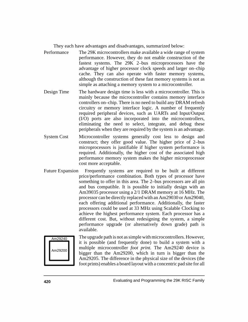
Am29200
Am29240
420 Evaluating and Programming the 29K RISC Family
They each have advantages and disadvantages, summarized below:Performance The 29K microcontrollers make available a wide range of system
performance. However, they do not enable construction of thefastest systems. The 29K 2–bus microprocessors have theadvantage of higher processor clock speeds and larger on–chipcache. They can also operate with faster memory systems,although the construction of these fast memory systems is not assimple as attaching a memory system to a microcontroller.
Design Time The hardware design time is less with a microcontroller. This ismainly because the microcontroller contains memory interfacecontrollers on–chip. There is no need to build any DRAM refreshcircuitry or memory interface logic. A number of frequentlyrequired peripheral devices, such as UARTs and Input/Output(I/O) ports are also incorporated into the microcontrollers,eliminating the need to select, integrate, and debug theseperipherals when they are required by the system is an advantage.
System Cost Microcontroller systems generally cost less to design andconstruct; they offer good value. The higher price of 2–busmicroprocessors is justifiable if higher system performance isrequired. Additionally, the higher cost of the associated highperformance memory system makes the higher microprocessorcost more acceptable.
Future Expansion Frequently systems are required to be built at differentprice/performance combination. Both types of processor havesomething to offer in this area. The 2–bus processors are all pinand bus compatible. It is possible to initially design with anAm39035 processor using a 2/1 DRAM memory at 16 MHz. Theprocessor can be directly replaced with an Am29030 or Am29040,each offering additional performance. Additionally, the fasterprocessors could be used at 33 MHz using Scalable Clocking toachieve the highest performance system. Each processor has adifferent cost. But, without redesigning the system, a simpleperformance upgrade (or alternatively down grade) path isavailable.
The upgrade path is not as simple with microcontrollers. However,it is possible (and frequently done) to build a system with amultiple microcontroller foot print. The Am29240 device isbigger than the Am29200, which in turn is bigger than theAm29205. The difference in the physical size of the devices (thefoot prints) enables a board layout with a concentric pad site for all

421Chapter 8 Selecting a Processor
three microcontrollers. Hence, the same board can be utilized withdifferent processors. However, because of the different accesstiming of DRAMs used by microcontrollers, it would be necessaryto also upgrade the memory devices. This does not generallypresent much of a problem. As a single board layout can easilyaccommodate different memory device speeds.
Peripherals Microcontrollers have the advantage of on–chip peripherals. Aswell as simplifying the design process, they enable a smaller boardlayout area and reduced system power consumption. The closecoupling of the on–chip peripherals to the processor, enables fastcommunication between the two, even at high clock speeds. Thereis also no extra cost for the peripherals.
Memory Choice When DRAM is used, microprocessors enable a wider range ofmemory systems to be constructed. The Am2920xmicrocontrollers only support 3/2 DRAM access (3–cycle firstaccess, thereafter 2–cycle burst). The higher performanceAm2924x microcontrollers only support 2/1 DRAM access.Burst–mode can be disabled resulting in slower 3/3 and 2/2memory access respectively, but there is little else that can bemodified. However, for many systems, the restrictions inherent inthe built–in microcontroller DRAM interface will present noproblem.
Board Size Microcontrollers are much more likely to enable a smaller boardlayout area. They have less need for peripheral support circuitry,particularly because of their built–in memory interfaces.
Power Consumption The Am2924x microcontrollers can operate at 3.3 volts andsupport power saving operating modes. Additionally,microcontroller based systems have less need for powerconsuming peripherals. This gives the microcontrollers theadvantage when constructing a low power system. However, theAm2920x low cost microcontrollers do not have the power savingfeatures. The only microprocessor particularly suited to lowpower systems is the Am29040. Because of its higher cost andhigher clock rate, its use is restricted higher performance systems.
Tool Selection User mode code is compatible across the entire 29K family. Thismeans, for instance, a C compiler can produce code for any of theprocessors. However, there are optimizations, such as the use ofinteger multiply with the Am29240 and Am29040 processors,which can improve a particular processor’s performance. Tool
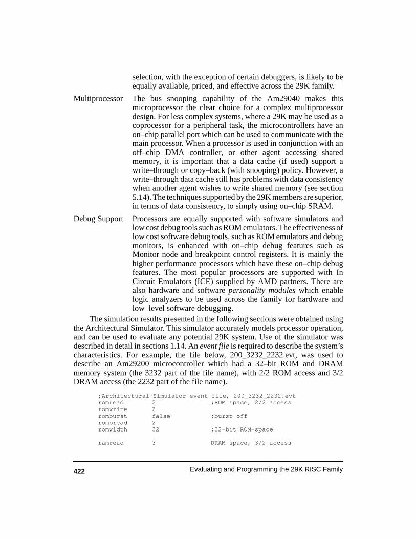
422 Evaluating and Programming the 29K RISC Family
selection, with the exception of certain debuggers, is likely to beequally available, priced, and effective across the 29K family.
Multiprocessor The bus snooping capability of the Am29040 makes thismicroprocessor the clear choice for a complex multiprocessordesign. For less complex systems, where a 29K may be used as acoprocessor for a peripheral task, the microcontrollers have anon–chip parallel port which can be used to communicate with themain processor. When a processor is used in conjunction with anoff–chip DMA controller, or other agent accessing sharedmemory, it is important that a data cache (if used) support awrite–through or copy–back (with snooping) policy. However, awrite–through data cache still has problems with data consistencywhen another agent wishes to write shared memory (see section5.14). The techniques supported by the 29K members are superior,in terms of data consistency, to simply using on–chip SRAM.
Debug Support Processors are equally supported with software simulators andlow cost debug tools such as ROM emulators. The effectiveness oflow cost software debug tools, such as ROM emulators and debugmonitors, is enhanced with on–chip debug features such asMonitor node and breakpoint control registers. It is mainly thehigher performance processors which have these on–chip debugfeatures. The most popular processors are supported with InCircuit Emulators (ICE) supplied by AMD partners. There arealso hardware and software personality modules which enablelogic analyzers to be used across the family for hardware andlow–level software debugging.
The simulation results presented in the following sections were obtained usingthe Architectural Simulator. This simulator accurately models processor operation,and can be used to evaluate any potential 29K system. Use of the simulator wasdescribed in detail in sections 1.14. An event file is required to describe the system’scharacteristics. For example, the file below, 200_3232_2232.evt, was used todescribe an Am29200 microcontroller which had a 32–bit ROM and DRAMmemory system (the 3232 part of the file name), with 2/2 ROM access and 3/2DRAM access (the 2232 part of the file name).
;Architectural Simulator event file, 200_3232_2232.evtromread 2 ;ROM space, 2/2 accessromwrite 2romburst false ;burst offrombread 2romwidth 32 ;32–bit ROM–space
ramread 3 DRAM space, 3/2 access

423Chapter 8 Selecting a Processor
ramwrite 3rampage true ;pagemode onrampread 2rampwrite 2ramwidth 32 ;32–bit DRAM space
By building new event files, it is possible to re–run simulations and evaluate theeffect on the system’s performance. The simulator was run using the commandbelow:
sim29 –29200 –e 200_3232_2232.evt a.out
The program being simulated, shown as a.out above, was the LAPDbenchmark. I chose to use LAPD rather than Stanford because of the high instructioncache hit ratio of the Stanford benchmark –– above 90% with even very small caches.I believe modeling the performance of LAPD is more likely to reflect the actualperformance most users will experience with their own application code. However,as always, I urge you to use your own code when benchmarking various processors.The LAPD benchmark is good at testing data movement and bit field (packet header)operations, but this may not be your requirement. Additionally, the Metawarecompiler was used with a high level of optimization (–07) when compiling thebenchmark. This produces the best performance but may require additional memoryto hold the expanded code which results from such optimizations as loop unrolling.
8.1.1 Selecting a Microcontroller
Microcontrollers are studied and grouped in this section according to theirmemory system speed. Initially, systems based on 16 MHz memory are analyzed.The performance of both 16– and 32–bit wide memories is presented. However, no8–bit systems are included. Very small systems based on 8–bit memories and usingthe Am2920x microcontrollers are evaluated in a separate section (section 8.1.2,Moving up to an Am2920x Microcontroller). Memory systems operating at 12.5MHz are also dealt with in the section dealing with very small systems.
16 MHz Memory SystemsSetting 12.5 MHz systems aside, 16 MHz is the entry level system speed. This
can be achieved using a 16 MHz Am29200, Am29205 or Am29245 processor, or anAm29240 using Scalable Clocking. When Scalable Clocking technology is used, a33 MHz Processor would be combined with a 16 MHz memory system. Bothinstruction and data accesses are satisfied by the slower 16 MHz memory. Thesimulation results for various systems running the LAPD benchmark are shown inFigure 8-1. Memory access times for the evaluated systems are shown in thenotation: (initial/subsequent), for example 2/1.
Programmable Data width was used to model 16–bit and 32–bit memories. Asexpected and supported by the results, the 16–bit memory systems offer less

424 Evaluating and Programming the 29K RISC Family
Figure 8-1. 29K Microcontrollers Running the LAPD BenchmarkWith 16 MHz Memory Systems
32–bit memory32–bit memory at 1/2 CPU speed
ÈÈÈÈ
16–bit memoryÍÍÍÍ
16–bit memory at 1/2 CPU speed
Packets per second
ÈÈÈÈÈÈÍÍÈÈÈÈ
ÈÈÈÈÍÍÈÈÈÈ
ÈÈÈÈÍÍÈÈÍÍÈÈÍÍÈÈÈÈÈÈ
ÈÈÈÈÈÈÍÍÈÈÈÈÈÈ
ÈÈÈÈÈÈÍÍÈÈÈÈÈÈ
ÈÈÈÈÈÈÍÍÈÈÍÍÈÈÈÈÈÈ
ÈÈÈÈÈÈÍÍÈÍÈÍÈÍÈÍÈÍÈÍÍÍÍÍÍÍÍÍÍ
ÍÍÍÍÍÍÍÍÍÈÈÍÍÍÍÍÍÍÍÍÍÍÍÍ
ÍÍÍÍÍÍÍÍÍÍÍÍÍÍÍÍÍÍÍÍÍÍ
ÈÍÈÍÈÍÈÍÈÍÈÍ
ÈÍÈÍ
0 1000 2000 3000 4000 5000 6000 7000 8000 9000 10000
205 */* 3/2
205 2/2 3/2
205 2/2 */*
200 */* 3/2
205 2/1 3/2
205 1/1 3/2
205 2/1 */*
245 */* 2/1
200 2/2 3/2
205 1/1 */*
200 2/2 */*
200 2/1 3/2
245 */* 2/1
245 2/2 */*
200 2/1 */*
245 2/2 2/1
240 */* 2/1
200 1/1 3/2
240 1/1 2/1
240 1/1 */*
240 2/2 */*
240 2/2 2/1
200 1/1 */*
245 1/1 */*
245 1/1 2/1
240 */* 2/1
240 1/1 2/1
240 1/1 */*
ROM orSRAMmemoryaccess
DRAMmemoryaccess
Am29
Am29
Am29
Am29
Am29
Am29
Am29
Am29
Am29
Am29
Am29
Am29
Am29
Am29
Am29
Am29
Am29
Am29
Am29
Am29
Am29
Am29
Am29
Am29
Am29
Am29
Am29
Am29
SRAM
SRAM
SRAM
biggeris better

425Chapter 8 Selecting a Processor
performance. Not all of the modeled systems are likely candidates for construction.They are shown merely to report their relative performance. Some of the mostinteresting systems are highlighted. For example, the second from the top entryshows an Am29205 system with 16–bit 2/2 ROM and 3/2 DRAM. This is an entrylevel system. The first entry shows an Am29205 operating from 16–bit DRAMalone. The notation “*/*” in the ROM/SRAM column indicates that no ROMmemory was used. Such a system would require initialization of the DRAM memory.This could be achieved with an 8–bit ROM which transferred its contents to DRAMbefore application code execution commenced. Note, it is not possible to build aDRAM–only system where a dual–ported DRAM is initialized by another processor.This is because after reset, program execution commences from ROM region 0. Thisdoes mean an SRAM–only system could be constructed; assuming that the SRAM islocated in ROM region 0, and is somehow initialized before processor reset.
The second entry, the 2/2–3/2 system, was linked such that instructions werefetched from the 2/2 ROM space; all data was accessed from the 3/2 DRAM. Thecombined ROM–DRAM system is faster than the 3/2 DRAM–only system. TheDRAM–only system has 81% of the faster system’s performance. This is due toinstruction accesses being directed to the faster 2/2 memory and the frequentoccurrence of DRAM precharge cycles. The Am29200 DRAM is frequently referredto as 3/2, this assumes the 1–cycle of RAS–precharge is hidden. When DRAM–onlysystems are used, the precharge is not likely to be hidden, and the access is truly 4/2rather than 3/2. This is explained in section 1.14.1 under the Am29200 and Am29205subheading. Given that even inexpensive EPROM devices can be 1.5 to 2–times thecost of DRAM (per byte), it is less expensive to use a single 8–bit EPROM toinitialize the DRAM, and then execute the program from DRAM. However, there is aloss of performance with this technique.
The sixth entry shows an Am29205 system with 1/1 ROM and 3/2 DRAM. Thesystem has substantially increased performance over the 2/2 ROM system (66%faster). The notation 1/1 is used here to indicate instruction read access times only.The microcontroller family requires one wait state when writing to ROM space. Thisresults in a minimum write access time of 2–cycles for ROM space. Although this isimportant to note, it has no impact here as the system performs all data writes toDRAM. However, the system is unbuildable due to the unavailability of ROMdevices which can deal with the very fast access times.
The access times for ROM space are determined by three parameters. First, theperiod of the memory system clock (CP) –– all memory accesses are synchronized tothe system clock. Second, the delay before synchronous outputs become valid (OV).Third, the input setup time (IS) for synchronous input signals. When performingsingle–cycle memory access, the access time is determined from the ROMOE signalbecoming valid after the falling edge of MEMCLCK (OVF). When wait states (WS)are used, the access time is determined from the address outputs becoming valid after

426 Evaluating and Programming the 29K RISC Family
Memory Bus Clock Period Output Valid Input Setup Memory Access Times (ns)Speed (MHz) (CP ns) (OVR, OVF ns) (IS ns) 0–Wait 1–Wait 2–Wait
12.5 80 15, 15 12 13 133 21316 62.5 11, 10 10 11.25 105 167.520 50 11, 10 10 5 79 129
Table 8-1. Memory Access Times for Am2920x Microcontroller ROM Space
the rising edge of MEMCLK (OVR). The equations below can be used to calculatethe required minimum memory access times.
Memory Access Time =(Clock Period)/2 –(Output Valid) –(Input Setup)=(CP/2) – OV F – IS ,WS=0
Memory Access Time =(Period)*(1+Wait States)–(Output Valid)–(Input Setup)=(CP * (1 + WS)) – OV R – IS ,WS > 0
Shown on Table 8-1 are the required memory access times for Am2920x ROMspace memory. The 1/1 access times are given under the zero wait state column. At16 MHz, an 11.25 ns access time must be supported. ROM devices at this speed arenot available. However, the access times for 2/2 ROM (1–wait) are reasonable, andcan be achieved with readily available 90 ns ROM devices.
It is not until a 20 MHz memory system is required that particularly fast ROMneed be used. At this stage an interleaved ROM system could be built or faster ROMpurchased for a higher cost. Alternatively, FLASH memory could be used. FLASH isgenerally available with faster access times than EPROM. Table 8-2 lists a number ofcurrent AMD memory devices and their access times. Faster and larger devices arealways being developed by AMD and other manufactures. It is likely that before longnew memory devices will become available and enable faster systems to beconstructed at lower cost.
The ninth entry shows a 32–bit Am29200 based system using 2/2 ROM and 3/2DRAM. This may be a popular system for construction. The 32–bit DRAM–onlysystem has only 71% of the combined ROM–DRAM system. Thus, the addition of32–bit wide ROM will be justifiable for those systems requiring extra performance.
Faster DRAM–based systems can be constructed using the 2/1 DRAMcontroller incorporated into the more expensive Am2924x microcontrollers. TheAm29245 is the least expensive, and it is shown with a 32–bit DRAM–only system(*/* 2/1) in entry thirteen of the table. The previous Am29200 system based onROM–DRAM, has only 71% of the performance of the DRAM–only Am29245system. Interestingly, the Am29240 system using 16–bit DRAM and ScalableClocking is shown to be faster than the Am29245 using 32–bit DRAM. This is due tothe higher internal clock rate and data cache of the Am29240.

427Chapter 8 Selecting a Processor
AMD Device Speeds (ns) Capacity Memory Type
Am27C010 90, 120, 150 128k x 8 EPROMAm27C020 80, 120, 150 256k x 8 EPROMAm27C040 90, 120, 150 512k x 8 EPROMAm27C080 90, 120, 150 1M x 8 EPROM
Am28F010 90, 120, 150 128k x 8 FLASHAm28F020 90, 120, 150 256k x 8 FLASHAm29F010 45, 55, 70 128k x 8 FLASHAm29F040 70, 90, 120 512k x 8 FLASH
Table 8-2. ROM and FLASH Memory Device Access Times
The fastest DRAM–only system, third from the bottom, is an Am29240 usingScalable Clocking and 32–bit DRAM. This system is 130% faster than the examinedAm29200 using ROM–DRAM. However, it is more expensive due to the premiumspeed microcontroller. An alternative is to use a less expensive Am29200 withSRAM. Shown on Figure 8-1 is a 32–bit 1/1 SRAM based system which is 100%faster than the studied ROM–DRAM system. When examining SRAM–onlysystems (such as the 1/1 */* example), the benchmark program was linked such thatboth instructions and data where accessed from SRAM. In practice this would likelyrequire programs to be located in 8–bit ROM, and transferred to SRAM during theinitialization stage. Unfortunately, SRAM is about eight times the cost of DRAM ona per–byte basis. However, if only a small amount of SRAM is required, the systemmay be cost effective, given the lower processor cost. At 12.5 MHz, zero wait stateaccess requires 13 ns SRAM. Such devices are readily available.
Table 8-3. Memory Access Times for Am2924x Microcontroller ROM Space
Memory Bus Clock Period Output Valid Input Setup Memory Access Times (ns)Speed (MHz) (CP ns) (OVR, OVF ns) (IS ns) 0–Wait 1–Wait 2–Wait
16 62.5 10, 9 7 15.25 108 170.520 50 10, 9 7 9 83 13325 40 10, 9 7 4 63 10333 31.25 10, 9 7 – 45.5 76.75
20 MHz Memory Systems
Microcontroller based systems using 20 MHz memory systems are shown inFigure 8-2 When using DRAM, these systems are always faster than 16 MHzsystems. However, a 20 MHz Am29200 system using 2/2 ROM and 3/2 DRAM hasonly 62% of the performance of a 16 MHz SRAM system.
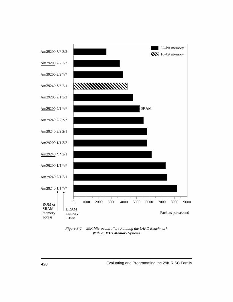
428 Evaluating and Programming the 29K RISC Family
Figure 8-2. 29K Microcontrollers Running the LAPD BenchmarkWith 20 MHz Memory Systems
ÈÈÍÍÈÈÍÍÈÈÍÍ
ÈÈÈÈÈÈÈÈÈÈÈÈÈÈÈÈÈÈÈÈ
ÍÍÈÈÍÍÈÈÍÍÈÈÈ
ÍÍÍÈÈÈ
ÍÍÍÈÈÍÍÈÈÍÍ
ÈÈÍÍÈÈÍÍÈÈÍÍ
0 1000 2000 3000 4000 5000 6000 7000 8000 9000
200 */* 3/2
200 2/2 3/2
200 2/2 */*
240 */* 2/1
200 2/1 3/2
200 2/1 */*
240 2/2 */*
240 2/2 2/1
200 1/1 3/2
240 */* 2/1
200 1/1 */*
240 2/1 2/1
240 1/1 */*
32–bit memoryÈÈÈÈÈÈ
16–bit memory
Packets per second
ROM orSRAMmemoryaccess
DRAMmemoryaccess
Am29
Am29
Am29
Am29
Am29
Am29
Am29
Am29
Am29
Am29
Am29
Am29
Am29
SRAM

429Chapter 8 Selecting a Processor
Building an Am29200 system with 1/1 SRAM at 20 MHz requires 5 ns memoryaccess times. These are much more expensive than the 11.25 ns memories required at16 MHz. To reduce cost, an interleaved SRAM system could be constructed. Thiswould result in 2/1 SRAM access. However, this achieves only 90% of theperformance on an 1/1 SRAM system operating at 16 MHz. It would be better tobuild the slower, less expensive, yet higher performing 16 MHz system.
With 20 MHz memory systems, the Am2920x microcontrollers are operating attheir maximum frequency. As more performance is required, the likelihood ofselecting an Am29240 processor increases. This is particularly true if DRAM–only isto be used. An Am29240 using 32–bit DRAM–only (2/1) is 151% faster than anAm29200 using a 3/2 DRAM–only system.
It is possible to build SRAM based systems using an Am29240 processor.Shown in Table 8-3 are the required memory access times for Am2924x ROM spacememory. The table is based on preliminary AMD data which may change in thefuture. The 1/1 access times are given under the 0–Wait column. At 20 MHz a 9 nsaccess time must be supported. This is difficult to achieve, and probably notworthwhile economically. In practice, it would be better to slow the clock speeddown to 19.2 MHz and use 10 ns SRAM devices.
However, the Am29240 system using 32–bit 2/1 DRAM–only has 76% of theperformance of a 32–bit 1/1 SRAM system. The performance benefit of SRAM,relative to DRAM, is diminished when used with an Am2924x microcontroller. Thisis partly due to the 2–cycle requirement for all data writes performed to ROM space.The 1/1 access is only achieved with instruction fetching and data reading. All datawrites are performed with, at best, 2/2 access times. Conversely, DRAM supports 2/1for all types of access.
25 MHz Memory Systems
The performance of 25 MHz memory systems is shown in Figure 8-3. Thesesystems can only be built using Am29240 and Am29243 microcontrollers. At thisspeed it is not possible to use 1–cycle first access memory. And, 2/1 SRAM haspoorer performance than 2/1 DRAM due to the 2–cycle data–write limitation.
Scalable Clocking is not available at 20 MHz and above. Hence, all memorysystems must run at the speed of the processor. The fast (2/1) DRAM controllerincorporated into the Am2924x microcontrollers makes DRAM the correct memorychoice with these processors. Additionally, the 2/2 ROM which could be used withsuch systems would degrade performance from a DRAM–only system. Hence, itmakes sense to use only a slow 8–bit ROM to initialize the DRAM. Program code,and initialized data, should be transferred from narrow ROM to DRAM duringprogram initialization. If a program is too large to fit within a single 8–bit ROM, itwould then make sense to use 16–bit ROM for additional capacity.

430 Evaluating and Programming the 29K RISC Family
Figure 8-3. 29K Microcontrollers Running the LAPD BenchmarkWith 25 MHz Memory Systems
ÈÈÈÈÈÈÈÈÈÈÈÈÈÈÈÈ
ÍÍ
ÈÈÍÍÈÈÍÍÈÈÍÍÈÈÍÍÈÈÈ
ÍÍÍ
0 2000 4000 6000 8000 10000 12000 14000
240 */* 2/1
240 2/2 */*
240 2/2 2/1
240 */* 2/1
240 2/1 2/1
240 1/1 */*
32–bit memoryÈÈÈÈÈÈ
16–bit memory
Packets per second
ROM orSRAM
DRAM
Am29
Am29
Am29
Am29
Am29
Am29
When executing from DRAM there is always the danger of accidentally writingto memory holding instructions and damaging the program. This can be avoided byusing the on–chip MMU to protect the relevant memory regions (see section 7.4.5).
33 MHz Memory Systems
The performance of systems operating at 33 MHz is shown in Figure 8-4. Aswith 25 MHz systems, 2/1 DRAM–only memory is most practical. At 25 and 33 MHzthe choice of systems which are practical is limited compared to the selection at 16 oreven 20 MHz. In fact the word “practical” should not be interpreted to mean easy orreadily available. At 33 MHz a DRAM system is challenged to meet the 2–1 timingspecification. Currently only the fastest DRAM devices are usable. For example,DRAM with 60 ns access times is required by 25 MHz systems. The most practicalway to use 33 MHz processors is with Scalable Clocking which reduces the memorysystem speed to 16 MHz. At these higher clock rates, the Am29240 microcontrolleris able to perform as well as many systems build around a 2–bus microprocessor.
Further Observations
Memory system requirement is not likely to be the only influence on processorselection. The Am2924x microcontrollers offer additional on–chip peripheralscompared to the Am2920x processors. This may direct processor selection towards

431Chapter 8 Selecting a Processor
Figure 8-4. 29K Microcontrollers Running the LAPD BenchmarkWith 33 MHz Memory Systems
ÈÈÈÈÈÈÈÈÈÈÈÈÈÈÈÈÈÈÈÈÈÈ
ÍÍ
ÈÈÍÍÈÈÈ
ÍÍÍÈÈÈ
ÍÍÍ È
ÈÈ
ÍÍÍ
0 2000 4000 6000 8000 10000 12000 14000
240 */* 2/1
240 2/2 */*
240 2/2 2/1
240 */* 2/1
240 2/1 2/1
32–bit memory
ÈÈÈ16–bit memory
Packets per second
Am29
Am29
Am29
Am29
Am29
ROM orSRAM
DRAM
the more expensive Am2924x grouping. Additionally the Am2924x processors haveadditional power saving features. Note, as a means of saving power, the Am2920xcan be temporarily clocked down to 8 MHz, and when necessary the clock returned tothe normal (higher) operating speed.
All microcontrollers are able to use interrupt context caching (see section 2.5.4).This improves interrupt processing and is somewhat independent of the off–chipmemory system performance. With interrupt context caching, the processor state issaved and restored from on–chip registers rather than external memory stack. Hence,even the least expensive system can support interrupts with a performance matchingthat of the more expensive systems.
8.1.2 Moving up to an Am2920x Microcontroller
This section presents the performance of Am2920x microcontrollers operatingat 12.5 and 16 MHz. The intention is to evaluate the smallest, least expensive systemspossible. This section should be of interest to the designer looking to use a RISCmicrocontroller to upgrade a system which would have previously used aninexpensive CISC processor. The performance of various 8–bit and 16–bit memorysystems is shown on Figure 8-5.
Much of the information presented in the previous 16 MHz microcontrollersection is applicable to the low cost systems studied here. There are three systems ofprimary interest. These systems can be constructed at both frequencies of interest.First, systems which operate with 16–bit DRAM–only including all systems which
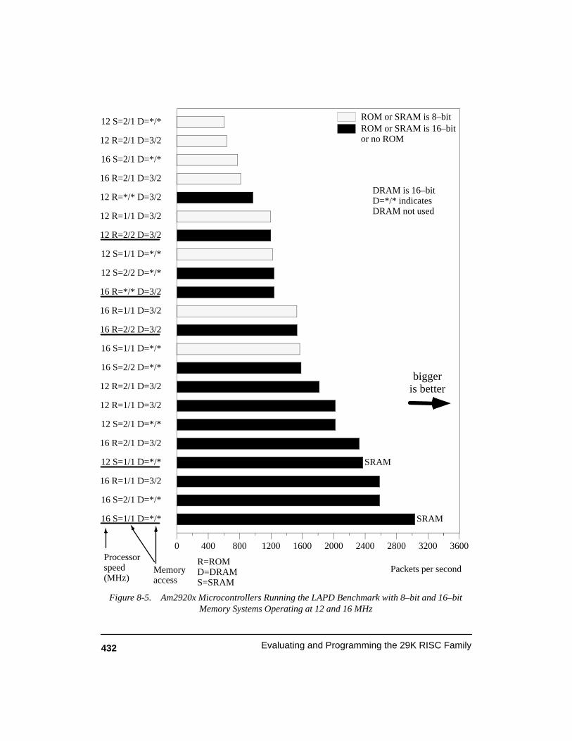
432 Evaluating and Programming the 29K RISC Family
Figure 8-5. Am2920x Microcontrollers Running the LAPD Benchmark with 8–bit and 16–bitMemory Systems Operating at 12 and 16 MHz
0 400 800 1200 1600 2000 2400 2800 3200 3600
12 S=2/1 D=*/*
12 R=2/1 D=3/2
16 S=2/1 D=*/*
16 R=2/1 D=3/2
12 R=*/* D=3/2
12 R=1/1 D=3/2
12 R=2/2 D=3/2
12 S=1/1 D=*/*
12 S=2/2 D=*/*
16 R=*/* D=3/2
16 R=1/1 D=3/2
16 R=2/2 D=3/2
16 S=1/1 D=*/*
16 S=2/2 D=*/*
12 R=2/1 D=3/2
12 R=1/1 D=3/2
12 S=2/1 D=*/*
16 R=2/1 D=3/2
12 S=1/1 D=*/*
16 R=1/1 D=3/2
16 S=2/1 D=*/*
16 S=1/1 D=*/*
ROM or SRAM is 8–bitROM or SRAM is 16–bitor no ROM
Packets per secondProcessorspeed(MHz)
Memoryaccess
R=ROMD=DRAMS=SRAM
DRAM is 16–bitD=*/* indicatesDRAM not used
SRAM
SRAM
biggeris better

433Chapter 8 Selecting a Processor
have slow ROM, or ROMs which are only 8–bits wide. Having slow or narrow ROMcan help to keep the system cost down. The program must be copied from ROM toDRAM after processor power up. Hence, the DRAM is the only memory whichinfluences program execution speeds. Unlike Am2924x microcontrollers theAm2920x processors have no Translation Look–Aside Buffers (TLBs).Consequently, they can not protect the DRAM from accidental damage duringprogram execution This may be more of an issue during code development than in afinal production product.
It is important to note here that the Am29205 processor does not have aBOOTW (boot width) pin, and hence must initially operate from 16–bit widememory. Only the Am29200 processor operation can be initiated from 8–bit ROM.Consequently, DRAM–only systems are more applicable to the Am29200. This is alittle unfortunate as only the Am29205 is available at the lower cost 12.5 MHzfrequency. Highlighted on Figure 8-5 are the simulation results for an Am29200processor operating at 16 MHz using DRAM–only (16 R=*/* D=3/2).
The second type of system of interest uses 16–bit ROM (2/2) with 16–bitDRAM (3/2). This is faster than operating from DRAM–only. If ROM is to be used itmust at least support 2/2 access or faster. Additionally, it must be 16–bits wide. If it isslower or narrower it is best to execute from DRAM–only. A 12.5 MHz Am29205with ROM (2/2) and DRAM (3/2) has 97% of the performance of a 16 MHzAm29200 operating at 16 MHz with DRAM–only.
The third type of system of interest uses 1/1 SRAM. Given the higher cost ofSRAM compared to DRAM, this configuration is only applicable when extraperformance is required. The SRAM–only systems shown in Figure 8-5 wouldrequire an 8–bit ROM for program initialization –– much the same as DRAM–onlysystems. The simulation results show that a 16–bit DRAM–only system has only79% of the performance of an 8–bit 1/1 SRAM system. The 8–bit SRAM system has2% more performance than the 16–bit 2/2–3/2 system (ROM–DRAM). The reasonfor the higher performance can be understood by examining the number of cyclesrequired to fetch a single 32–bit instruction. With a 16–bit 3/2 DRAM–only system,6–cycles are required to fetch the first instruction; 4–cycles for burst–mode fetchedinstructions. With 8–bit 1/1 SRAM, 4–cycles are required to fetch instructions. The8–bit SRAM has the advantage.
Building a 16–bit SRAM system which is 1/1 produces a system which has140% of the performance of a 16–bit DRAM–only system. At 12.5 MHz,single–cycle access requires 13 ns SRAM, which is readily available. Simple SRAMbased designs can offer surprisingly good performance but the small size of SRAMdevices results in the systems only being suitable for applications requiring smallamounts of memory. Otherwise the cost of the SRAM is likely to be prohibitivelyhigh.

434 Evaluating and Programming the 29K RISC Family
8.1.3 Selecting a Microprocessor
The highest performance systems are constructed around 2–bus 29Kprocessors. The following subsections present the performances obtained for acomplete range of 29K processors running the LAPD benchmark. Systems arestudied and grouped in subsections according to their memory system speed. Allvalues were obtained using 32–bit DRAM or SRAM memory systems. Processorsran, as indicated, at the same speed as the system memory or at two–times usingScalable Clocking technology. Comparing the fastest and slowest systems, there is aperformance difference of more than 6–to–1. There is also a range of inbetweensystems which offer a wide selection of performance configurations.
DRAM is frequently referred to as, say, 2/1. This assumes the often required1–cycle of precharge (RAS precharge) is hidden. When DRAM–only systems areconstructed, the precharge encountered when accessing a new memory page can notalways be hidden, and the access is thus 3/1 rather than 2/1. This is explained insection 1.14.1 under the Am29200 and Am29205 subheading. The previous sectionon selecting a microcontroller also referred to DRAM memory speeds withoutincluding the necessary precharge time. The terminology is acceptable because theprecharge can frequently be hidden when the ROM region is used in conjunction withthe DRAM region. Consequently precharge has little effect on performance.However, when DRAM–only systems are constructed, the effect precharge has onsystem performance is more noticeable. Even if a 2/1 DRAM–only system suffers a1–cycle precharge on all new page accesses, thus resulting in a 3/1 access, it shall stillbe termed 2/1. Consistently maintaining the same notation for memory accessthroughout this book helps with system comparisons. In summary, a 2/1 DRAM has2–cycle initial access followed by 1–cycle for same–page accesses. WithDRAM–only systems a 2/1 system equates to a 3/1 system for all new page accesses.
With microcontrollers, the access times for the DRAM memory regioncontroller are built into the Architectural Simulator. Constructing an event file for2–bus processors is a little more difficult. The event file shown below describes a 2/1DRAM system used with a 2–bus processor. The required precharge and refreshtimes are included. These parameters are also built into the simulation model formicrocontrollers. If a 2/1 SRAM system was being modeled, the precharge andrefresh parameters would be omitted. Note, in the example, Scalable Clocking is notselected.
;Architectural Simulator event filespacerambank 80000000 100000 ;memory locationramwidth 32 ;32–bit DRAMramread 2 ;2/1 accessramwrite 2ramburst true ;burst enablerambread 1rambwrite 1

435Chapter 8 Selecting a Processor
halfspeedbus false ;no Scalable Clockingramprecharge 1 ;DRAM prechargerampprecharge 2ramrefresh 255 ;DRAM refresh
The LAPD program was linked and then simulated operating from DRAM– orSRAM–only memory. Systems using mixed DRAM and SRAM were not modeled.It is certainly possible to use SRAM; although the cost is likely to be relatively high,given the generally large memory systems attached to 2–bus processors. However,ROM devices are likely to be used with 2–bus processors; but since it is difficult toachieve 1–cycle access with ROM, it is likely that data and code held in ROM wouldbe transferred to DRAM for faster access. Alternatively, an interleaved ROM systemmay be constructed. This would enable 2/2 ROM to achieve 2/1 memory access;resulting in much the same performance as 2/1 DRAM. In fact faster, as there is noneed to perform precharge when changing access to a new memory page.
The Am29050 3–bus processor results have been included with the 2–busresults. The Am29050 is the only member of the 3–bus processor group which islikely to be selected for a new design. A 2–bus processor such as the Am29030 offersas much performance as a 3–bus Am29000; and also offers a simpler system design,as well as an easier upgrade path. The inclusion of a floating–point execution unitwithin the Am29050 makes it an attractive choice for floating–point intensiveoperations. Two–bus processors perform floating–point operations using emulationroutines generally accessed via traps. This is slower than the direct executionachieved with the Am29050. However, the Am29040 can perform integer multiplydirectly in hardware (other 2–bus processors use emulation), this assists the task ofemulating missing floating–point operations. Consequently, the Am29040 processoris an alternative to the Am29050 when an application requires fast floating–pointsupport. The LAPD benchmark does not contain any floating–point operations.Hence, it is not a suitable benchmark for evaluating processors for floating–pointoperation.
16 MHz Memory Systems
This is the entry level system speed for 2–bus processors. The Am29035 is theonly processor offered at this speed. However, using Scalable Clocking an Am29030or Am29040 operating at 33 MHz internally, can be combined with a 16 MHzmemory system. When Scalable Clocking is used, off–chip instruction and dataaccess is performed at the slower 16 MHz memory system speed. The higher cost ofthe faster processors makes these systems more expensive, but a considerably morepowerful systems is achieved. Figure 8-6 shows performance results for varioussystems based on 16 MHz memory systems.
The performance of the systems improve in accordance with the availability offaster memory. Given that all 2–bus 29K processors contain instruction cache,off–chip access is mainly required for instruction cache reload. Caches which

436 Evaluating and Programming the 29K RISC Family
support only one valid–bit per block, always fetch a complete block before markingthe block valid. The Am29040 which has a valid–bit for each entry in the block,fetches only the instructions required for execution. Table 8-4 gives the cache reloadtime for various memory systems, assuming a complete block is fetched. DRAMaccess times include precharge time.
Relative system performance is ordered in accordance with the cache blockreload times shown in Table 8-4. Using an Am29035, the slowest 3/2 DRAM systemhas 70% of the performance of the fastest 2/1 DRAM system. However, ScalableClocking enables the Am29035, to be replaced with an Am29030 which improvesthe performance of the 2/1 system by 93%. Selecting an Am29040 improves theperformance by 192%. The 33 MHz processors cost more but they enable threeprice–performance combinations by merely replacing the pin–compatibleprocessors and doubling the clock frequency.
At 16 MHz the 62.5 ns clock period makes a 2/1 DRAM design feasible usingreadily available 80 ns DRAMs. During a page mode access RAS is held active, andthe access time after asserting the CAS is typically 30 ns. Assuming CAS prechargetimes of 15 ns (the interval CAS is held high between consecutive accesses), the timerequired to complete an access within the page is 45 ns. In practice it is likely to be alittle more due to support circuity such as PAL devices. This adds an additional 5 to10 ns to the access time. Hence, the total access time for the current page is about 55ns, under the 62.5 ns necessary for 1–cycle burst access. Allowing 2–cycle firstaccess provides 125 ns, which exceeds the typical 80 ns access time for DRAM. Ofcourse, if precharge is required the RAS must be held high for an additional 60 ns(typically) before a new page address is established and RAS brought low. Moresophisticated systems can bring the RAS signal high while CAS is still asserted. Thisenables RAS precharge to start early and can help eliminate all or some of the RASprecharge time. The results for a 2/1 DRAM–only system are highlighted inFigure 8-6.
Memory Device Access Time(cycles)
Time to reload acache block (cycles)
DRAM 3/2 (3+1)+2+2+2 = 10
Table 8-4. Cache Block Reload Times for Various Memory Types
DRAM 3/1 (3+1)+1+1+1 = 7
DRAM 2/1 (2+1)+1+1+1 = 6
SRAM 3/2 (3)+2+2+2 = 9
SRAM 2/1 (2)+1+1+1 = 5
DRAM 2/2 (2+1)+2+2+2 = 9

437Chapter 8 Selecting a Processor
Figure 8-6. 29K Microprocessors Running the LAPD Benchmarkwith 16 MHz Memory systems
0 2000 4000 6000 8000 10000 12000 14000
Am29035 D=3/2
Am29035 S=3/2
Am29035 D=3/1
Am29035 D=2/1
Am29035 S=2/1
Am29030 D=3/2
Am29030 S=3/2
Am29030 D=3/1
Am29030 D=2/1
Am29030 S=2/1
Am29040 D=3/2
Am29040 S=3/2
Am29040 D=3/1
Am29040 D=2/1
Am29040 S=2/1
32–bit memory32–bit memory at 1/2 CPU speed
Packets per second
upgrade path
S=SRAMD=DRAM Memory access
biggeris better
438 Evaluating and Programming the 29K RISC Family
The instruction cache hit–ratio is 47.7% for the Am29035 using a 2/1 DRAMsystem. The Am29035 has the smallest instruction cache, 4k bytes. The Am29030and Am29040 have an instruction cache hit–ration of 95.1%. This is due to theirlarger 8K byte cache.
20 MHz Memory Systems
The performance of processors operating with 20 MHz memory systems isshown in Figure 8-7. The relatively inexpensive Am29035 processor is not availableat this or higher frequencies. With the Am29030 processor, the 3/2 SRAM system isfaster than the 3/1 DRAM. This is due to the higher cache hit–ratio of the Am29030compared to the Am29035. The larger cache reduces the impact cache reload has onperformance. However, it reveals the cost of data memory access which frequentlyoccurs with the LAPD benchmark. To access a single 32–bit data object costs4–cycles (1–cycle precharge plus 3–cycle access). The SRAM only requires3–cycles for the same task. Consequently, the SRAM, although it can not sustain1–cycle burst, is faster. Using the Am29040 processor, the 3/1 DRAM is again abetter choice than 3/2 SRAM. This is a result of the on–chip data cache reducing theeffects of memory precharge for data accesses.
The 50 ns period of a 20 MHz system clock makes 1–cycle burst–mode accesspossible using slightly faster DRAM. Additionally, 2–cycle first access (100 ns) ispossible with 80 ns DRAM. The 60 ns RAS precharge can be hidden if DRAM iscombined with ROM –– the precharge occurring during ROM access. Alternatively,DRAM access, including RAS precharge, is 140 ns (80+60) which is a really 3–cyclefor an initial new page access (150 ns).
The results for 2/1 and 2/2 DRAM–only systems are highlighted on Figure 8-7.Using an Am29030 processor, a 2/1 system has 15% more performance than the 2/2system. The difference is 24% when using an Am29040 processors. ScalableClocking enables the Am29030 to be replaced with an Am29040 which improves theperformance of the 2/2 system by 96%. With a 2/1 system, the performance isimproved by 112%.
25 MHz Memory Systems
The performance of processors operating with 25 MHz memory systems isshown in Figure 8-8. At 25 Mhz the cycle time is reduced to 40 ns. This makes1–cycle burst–mode access difficult to achieve. Lets look at the arithmetic; fastDRAMs have an access time of, say, 20 ns from CAS assertion, and 10 ns CASprecharge. Let’s also assume fast 5 ns PAL logic, and a best–case input setup time of 6ns (Am29040, 12 ns for the Am29030). This results in a total access time of 41 ns (47ns for the Am29030). This makes 1–cycle burst–mode impossible at 25 MHzwithout an interleaved memory system. However, an Am29040 could be operated at24 MHz and just achieve the timing requirements for 1–cycle burst–mode access. Aninitial 2–cycle access time can not be achieved with 80 ns DRAM. This would require

439Chapter 8 Selecting a Processor
Figure 8-7. 29K Microprocessors Running the LAPD Benchmarkwith 20 MHz Memory Systems
0 2000 4000 6000 8000 10000 12000 14000 16000
Am29030 D=3/2
Am29050 D=2/2
Am29030 D=2/2
Am29030 D=3/1
Am29030 S=3/2
Am29030 D=2/1
Am29030 S=2/1
Am29050 D=2/1
Am29040 D=3/2
Am29040 D=2/2
Am29040 S=3/2
Am29040 D=3/1
Am29040 D=2/1
Am29040 S=2/1
32–bit memory32–bit memory at 1/2 CPU speed
Packets per secondS=SRAMD=DRAM Memory access
I=2/2, D=2/2
I=2/1, D=2/1
upgrade path
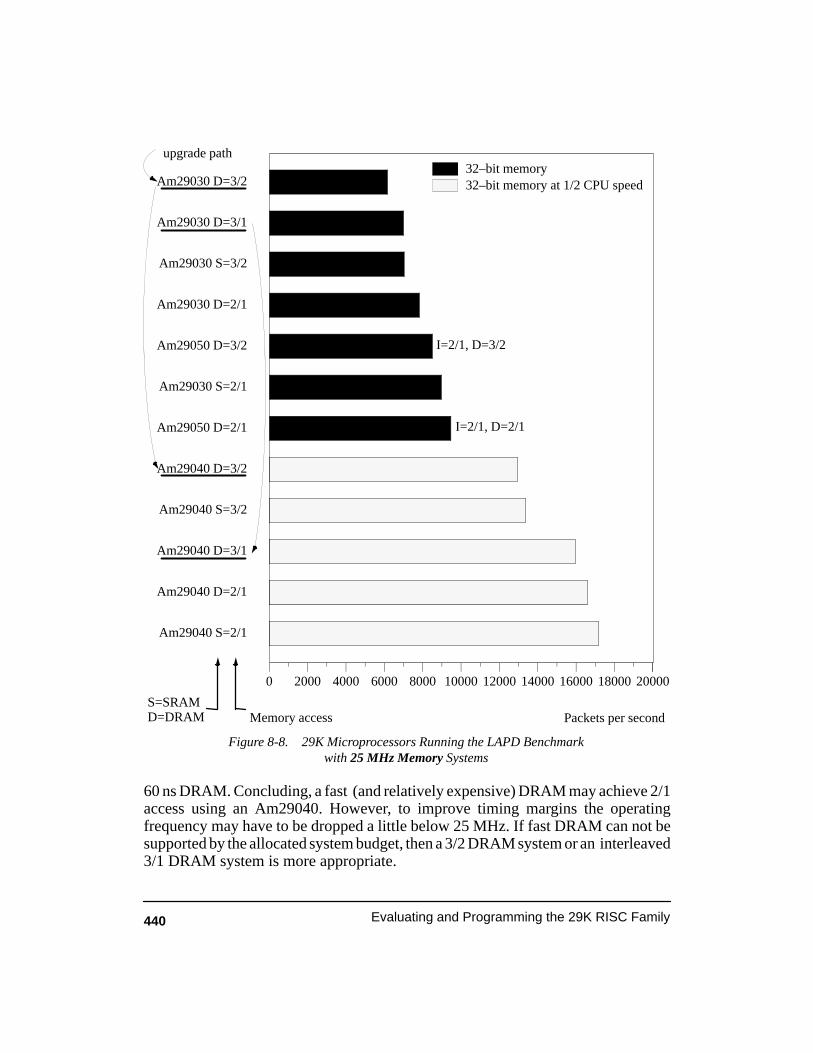
440 Evaluating and Programming the 29K RISC Family
Figure 8-8. 29K Microprocessors Running the LAPD Benchmarkwith 25 MHz Memory Systems
0 2000 4000 6000 8000 10000 12000 14000 16000 18000 20000
Am29030 D=3/2
Am29030 D=3/1
Am29030 S=3/2
Am29030 D=2/1
Am29050 D=3/2
Am29030 S=2/1
Am29050 D=2/1
Am29040 D=3/2
Am29040 S=3/2
Am29040 D=3/1
Am29040 D=2/1
Am29040 S=2/1
32–bit memory32–bit memory at 1/2 CPU speed
Packets per secondS=SRAMD=DRAM Memory access
I=2/1, D=3/2
I=2/1, D=2/1
upgrade path
60 ns DRAM. Concluding, a fast (and relatively expensive) DRAM may achieve 2/1access using an Am29040. However, to improve timing margins the operatingfrequency may have to be dropped a little below 25 MHz. If fast DRAM can not besupported by the allocated system budget, then a 3/2 DRAM system or an interleaved3/1 DRAM system is more appropriate.

441Chapter 8 Selecting a Processor
The LAPD benchmark results indicate that a 2/1 DRAM–only system is 27%faster than a 3/2 DRAM–only system. The interleaved 3/1 DRAM–only system is14% faster than the non–interleaved 3/2 DRAM–only system, and 23% faster for theclock scaled systems based on the Am29040. The results for 3/1 and 3/2DRAM–only systems are highlighted on Figure 8-8. Scalable Clocking enables theAm29030 to be replaced with an Am29040 which improves the performance of the3/2 system by 110%. With a 3/1 system, the performance is improved by 128%.
Note also that a system based on an Am29030 using 3/2 DRAM–only at 25MHz, has 2% lower performance than an Am29030 using 2/1 DRAM–only at 20MHz. Consequently, in this case, there is a performance advantage obtainable byreducing the memory system operating frequency.
33 MHz Memory Systems
The performance of processors operating with 33 MHz memory systems isshown in Figure 8-9. Scalable Clocking is no longer available with 33 MHz memorysystems. This places 33 MHz systems in competition with slower memory systemsusing clock scaled processors. It is not likely that construction of a memory systemfaster than 33 MHz would be practical. Clock rates such as 40 MHz would requireadditional memory wait states. Consequently, the system performance would be nofaster than a slower memory system operating with fewer memory access wait states.
Only the very fastest DRAMs and support circuitry could achieve 1–cycleburst–mode access without using an interleaved DRAM design. Achieving 2–cycleinitial access is also unlikely given the 31.25 ns Clock period. A 3–cycle (93.75 ns)first access seems more likely. The results for 3/1 and 3/2 DRAM–only systems arehighlighted on Figure 8-9.
The complexity of building a 3/1 rather than a 3/2 memory system at 33 Mhzmust be justified by a sufficient performance gain. Using an Am29030 processor aperformance gain of 13.6% is shown. With an Am29040, the performance gain is17.2%. However, using Scalable Clocking, an Am29040 (50 MHz) using 3/1 DRAMat 25 MHz is 41% faster than an Am29040 using 3/2 DRAM at 33 MHz; and 20%faster than an Am29040 using faster 3/1 DRAM at 33 MHz. An Am29040 operatingat 50 MHz with a 2/1 DRAM system operating at 25 MHz is the fastest DRAM–onlysystem benchmarked.
Additional Observations.
Setting the Am29050 aside due to its enhanced floating–point processingcapability, system performance is likely to be the main influence on processorselection. However, if low power consumption, 3.3–volt operation, ormulti–processor cache consistency are important issues, then the Am29040processor is the clear choice. Scalable Clocking technology clearly offers a majorperformance enhancement, but it does require the purchase of a more expensiveprocessor. This may be offset by a simpler memory system design which uses less

442 Evaluating and Programming the 29K RISC Family
Figure 8-9. 29K Microprocessors Running the LAPD Benchmarkwith 33 MHz Memory Systems
0 2000 4000 6000 8000 10000 12000 14000 16000
Am29050 D=3/2
Am29030 D=3/2
Am29030 D=3/1
Am29030 S=3/2
Am29050 D=3/1
Am29030 D=2/1
Am29040 D=3/2
Am29030 S=2/1
Am29040 S=3/2
Am29040 D=3/1
Am29040 D=2/1
Am29040 S=2/1
32–bit memory
Packets per second
I–space 3/2,D–space 3/2
I–space 3/1, D–space 3/1
upgrade path
S=SRAMD=DRAM Memory access
expensive DRAM components. Scalable Clocking and processor pin–compatibilitydoes simplify the task of creating multiple price–performance system configurations–– using a single board design.
All 29K processors are able to use interrupt context caching (see section 2.5.4).This improves interrupt processing and is somewhat independent of the off–chipmemory system performance. As with microcontrollers, even the least expensive

443Chapter 8 Selecting a Processor
2–bus microprocessor can support interrupts with a performance matching that of themore expensive systems.
The LAPD benchmark does not evaluate all of the performance parameterswhich are important to a real–time system. Performance parameters such as taskcontext switch time may also be important. Many non–application benchmarks areconcerned with movement of large amounts of data –– such as context saving andrestoring. Achieving single–cycle burst–mode for data access will greatly improvedata move operations which use store– and load–multiple operations.
8.1.4 Reducing the Register Window Size
As explained in section 2.3.2, the “lregs=n” switch can be used with the High C29K compiler to reduce the size of the register stack cache. That is, not all of the 128local register file need be allocated to caching the top of the run–time register stack.
The register cache is often referred to as the register window (window size = rfb– rab, see section 2.1.1). A reduced window size would increase the frequency ofstack spilling and filling, and consequently reduce the processors effectiveness at
Figure 8-10. Am29040 Microprocessors Running the LAPD Benchmarkwith Various Register Stack Window Sizes
0 2000 4000 6000 8000 10000 12000 14000 16000 18000 20000
36
48
64
80
96
112
128
Packets per second
Am29040 operating at 50 MHz, Memory is 2/1 DRAM operating at 25 MHz
Register Window size
biggeris better

444 Evaluating and Programming the 29K RISC Family
executing application code. However, in certain circumstances, task context switchtimes are reduced when operating with a smaller window size.
First, let’s look at the loss of performance resulting from adjusting the windowsize. The maximum window size is 128, and the minimum is 36 (a restriction set bythe “lregs” compiler option). Figure 8-10 shows performance results for anAm29040 microprocessor operating at 50 MHz with a 25 MHz 2/1 DRAM–onlymemory system. With the window reduced to 64, which is half its normal size of 128registers, a performance reduction of 9.2% was measured. With a window size ofonly 48, the performance is reduced by 15%.
The same LAPD performance measurements were acquired with an Am29200microcontroller operating with 3/2 DRAM. The results are shown on Figure 8-11.The performance drop–off with reduced window size is even less pronounced. With awindow size of 64, the reduction is only 5.2%, and 10% with a window size of 48.
The load– and store–multiple operations used by spill and fill handlers areperformed directly to memory. On–chip data cache has no effect on spill/fill data
Figure 8-11. Am29200 Microcontroller Running the LAPD Benchmarkwith Various Register Stack Window Sizes
0 300 600 900 1200 1500 1800 2100 2400 2700 3000
36
48
64
80
96
112
128
Packets per second
Memory is 3/2 DRAM operating at 20 MHz
Register Window size
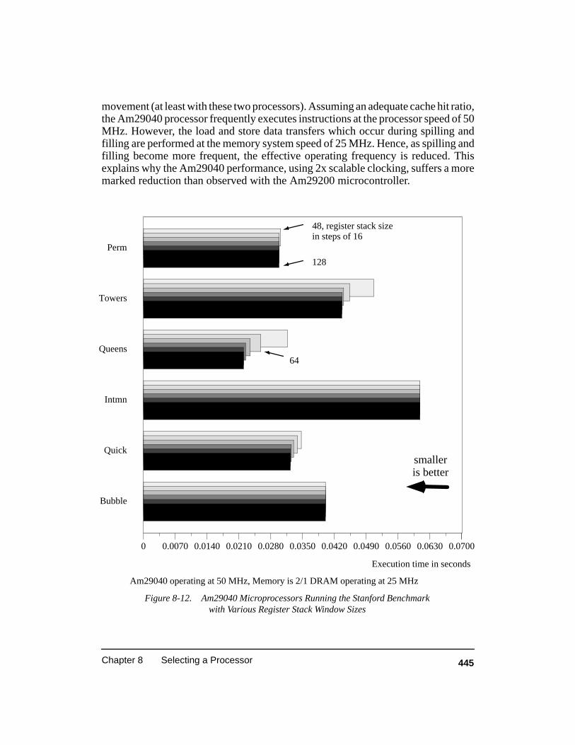
445Chapter 8 Selecting a Processor
movement (at least with these two processors). Assuming an adequate cache hit ratio,the Am29040 processor frequently executes instructions at the processor speed of 50MHz. However, the load and store data transfers which occur during spilling andfilling are performed at the memory system speed of 25 MHz. Hence, as spilling andfilling become more frequent, the effective operating frequency is reduced. Thisexplains why the Am29040 performance, using 2x scalable clocking, suffers a moremarked reduction than observed with the Am29200 microcontroller.
Figure 8-12. Am29040 Microprocessors Running the Stanford Benchmarkwith Various Register Stack Window Sizes
0 0.0070 0.0140 0.0210 0.0280 0.0350 0.0420 0.0490 0.0560 0.0630 0.0700
Perm
Towers
Queens
Intmn
Quick
Bubble
Execution time in seconds
Am29040 operating at 50 MHz, Memory is 2/1 DRAM operating at 25 MHz
48, register stack sizein steps of 16
128
smalleris better
64
446 Evaluating and Programming the 29K RISC Family
Some applications may be more, or less, affected by changes in the window size;it very much depends on the procedure’s register requirements and on the level ofprocedure nesting. To study these effects further, the Am29040 based system wasused to run the Stanford benchmark. Separate results for six of the integer routinestaken from the integer–part of the Stanford code are shown on Figure 8-12. Theroutines were chosen because of their diversity in function and similarity inexecution times. This similarity made for clearer scaling and hence easiercomparison of the results.
Routines which have a small register requirement are unaffected by thereduction in window size. The Towers and Queens tests are supported by recursiveprocedure calls. Consequently, these routines show a marked loss of performancewhen operating with reduced window sizes. The reduction in performance is lessthan one might expect. Applications which have a small dynamic register–stackrequirement, experience moderate loss of performance when operating with areduced window size. However, future 29K processors which use 3x or 4x scalableclocking technology and superscalar execution are likely to show a relatively greaterloss of performance with reduced window sizes. At higher execution speeds, the costof going off–chip is increased.
We have looked at the loss of performance associated with reduced windowsizes but what, if any, are the benefits? It was already stated that task contextswitching can be improved. This is true, but needs further explanation. Mostoperating system manufacturers provide basic context switch times for benchmarksrun on their product. These benchmarks typically indicate a raw context switch timeof 10 to 20 micro seconds. Longer or shorter times are possible depending on theimplementation and the speed of the system memory. Benchmark programs usuallymeasure synchronous context switch times; these are shorter than asynchronousswitch times. When a synchronously saved context is switched–in, only the currentactivation record need be restored in the register cache (typically 12 registers). Withan asynchronously saved context, the register cache must be restored to the positionat which the context was saved (several activation records). Hence, asynchronousswitches take longer than synchronous switches. How much longer depends on anumber of factors.
An operating system may be written in C, and the context switch code mayoccur at a depth of several levels of procedure nesting. As well as these operatingsystem related activation records, the register cache will contain activation recordsrelating to the application task. It is not possible to state, in general, just how much ofthe register cache is in use at the point the context switch occurs; but certainly theworst–case condition is known. The maximum number of local registers whichwould require saving or restoring is limited to the window size. Consequently,reducing the window size, reduces the worst–case context switch time. It will have

447Chapter 8 Selecting a Processor
less of an effect on average context switch times; and little, if any, on synchronouscontext switch times.
Task context switching is not a frequently occurring activity, compared toprocedure call and returns. Reducing the window size may improve context switchtimes, but at the cost of increasing the overhead associated with a more frequentlyoccurring event –– spilling and filling. However, for those systems which perform anunusually high number of task context switches, say 20,000 per second (one every 50micro seconds), it may make sense to operate with a reduced window size.Figure 8-13 shows the amount of time removed from the worst–case (save andrestore) task context switch times for various window sizes. Two memory systemsare presented; a 1–cycle memory at 25 MHz, and a 2–cycle memory at 16 MHz. Asthe window size is reduced, the savings increase.
�
�
��
��
��
��
� �� �� �� �� �� � ��� ���
Figure 8-13. Reduction In Worst–Case Asynchronous Task Context Switch Timeswith Various Register Stack Window Sizes
Window Size
Micro Seconds
16 MHz 2–cycleburst–mode
25 MHz 1–cycleburst–mode
Reducing the window size can be a benefit when interrupt processing. When aUser mode program is interrupted, it is normal to save the interrupted program’scontext in the Process Control Block (PCB), (see section 5.4). However, if no taskcontext switch will occur as a result of the interrupt, then it is faster to save the contextin the available register cache space.
Similarly, when a Supervisor mode program is interrupted, context is saved on amemory stack. This is the approach taken by the non–multitasking OS–bootoperating system supplied by AMD. Appendix B presents the interrupt context save

448 Evaluating and Programming the 29K RISC Family
code which can be used by a HIF conforming operating systems to prepare for signalprocessing. The example code saves context at the current memory stack position. Atotal of 51 32–bit words are required to save the complete context. If the cachewindow were reduced to 128–52=76 registers, there would be sufficient space tosave the interrupted context in the register file. The registers in the space (rfb–128) torab are not part of the window. In fact, registers below rsp (rsp to rfb–128) are alwaysavailable for interrupt handler use.

449Chapter 8 Selecting a Processor

450
Appendix A
HIF Service Calls
A.1 Service Call Numbers And Parameters
This section describes in detail each HIF 2.0 service. Service calls use local reg-isters to pass parameters to the operating system, global registers are used to returnresults. Example code sequences are given for each service. However, user code doesnot normally invoke HIF services directly. It is more likely an assembly languageglue routine or other library routine will be used to access the service. AMD supplieslibraries of the necessary glue code. Chapter 2 introduced the HIF concepts and hasan overview of its services.

451Appendix A HIF Service Calls
Service 1 – exit Terminate a Program
Description
This service terminates the current program and returns a value to the systemkernel, indicating the reason for termination. By convention, a zero passed in lr2 in-dicates normal termination, while any non-zero value indicates an abnormal termina-tion condition. There are no returned values in registers gr96 and gr121 since thisservice does not return.
Register Usage
Type Regs Contents Description
Calling: gr121 1 (0x1) Service numberlr2 exitcode User-supplied exit code
Returns: gr96 undefined This service call does not returngr121 undefined This service call does not return
Example Call
const lr2, 1 ;exit code = 1const gr121,1 ;service = 1asneq 69,gr1,gr1 ;call the operating system
In the above example, the operating system kernel is being called with servicecode 1 and an exit code of 1, which is interpreted according to the specifications of theindividual operating system. The value of the exit code is not defined as part of theHIF specification.
In general, however, an exit code of zero (0) specifies a normal program ter-mination condition, while a non-zero code specifies an abnormal termination result-ing from detection of an error condition within the program.
Programs can terminate normally by falling through the curly brace at the end ofthe main function in a C language program. Other languages may require an explicitcall to the kernel’s exit service.

452 Evaluating and Programming the 29K RISC Family
Service 17 – open Open a File
Description
This service opens a named file in a requested mode. Files must be explicitlyopened before any read, write , close, or other file positioning accesses can be ac-complished. The open service, if successful, returns an integer token that is used torefer to the file in all subsequent service requests. In many high-level languages thereturned token is referred to as a file descriptor. File names are generally not portablefrom one implementation to another. In some cases, names can be made more porta-ble by limiting them to six or fewer upper-case alphabetic characters, or by using thetmpnam HIF service (33) to create names that conform to the current implementa-tion’s file system requirements.
Environment variables can also be used to specify legal file names for applica-tion programs wishing to conform to the requirements of a particular HIF imple-mentation. The getenv service (65) provides the means to associate a file name orpathname with a mnemonic reference. This is the most portable means to specifypathnames for implementations that incorporate the getenv service.
The HIF specification intentionally refrains from defining the constituents of alegal pathname, or any intrinsic characteristics of the implemented file system. Inthis regard, the only requirement of a HIF-conforming kernel is that when the openservice is successfully performed, that the routine returns a small integer value thatcan be used in subsequent input/output service calls to refer to the opened file.
Register Usage
Type Regs Contents Description
Calling: gr121 17 (0x11) Service numberlr2 pathname A pointer to a filenamelr3 mode See parameter descriptions below.lr4 pflag See parameter descriptions below.
Returns: gr96 fileno Success:≥ 0 (file descriptor) Failure: < 0
gr121 0x80000000 Logical TRUE, service successful errcode Error number, service not successful
(implementation dependent)
Parameter Descriptions
Pathname is a pointer to a zero-terminated string that contains the full path andname of the file being opened. Individual operating systems have different means to
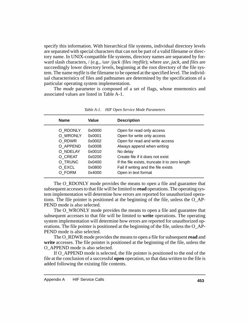
453Appendix A HIF Service Calls
specify this information. With hierarchical file systems, individual directory levelsare separated with special characters that can not be part of a valid filename or direc-tory name. In UNIX-compatible file systems, directory names are separated by for-ward slash characters, / (e.g., /usr /jack /files /myfile); where usr, jack, and files aresucceedingly lower directory levels, beginning at the root directory of the file sys-tem. The name myfile is the filename to be opened at the specified level. The individ-ual characteristics of files and pathnames are determined by the specifications of aparticular operating system implementation.
The mode parameter is composed of a set of flags, whose mnemonics andassociated values are listed in Table A-1.
Table A-1. HIF Open Service Mode Parameters
Name Value Description
O_RDONLY 0x0000 Open for read only accessO_WRONLY 0x0001 Open for write only accessO_RDWR 0x0002 Open for read and write accessO_APPEND 0x0008 Always append when writingO_NDELAY 0x0010 No delayO_CREAT 0x0200 Create file if it does not existO_TRUNC 0x0400 If the file exists, truncate it to zero lengthO_EXCL 0x0800 Fail if writing and the file existsO_FORM 0x4000 Open in text format
The O_RDONLY mode provides the means to open a file and guarantee thatsubsequent accesses to that file will be limited to read operations. The operating sys-tem implementation will determine how errors are reported for unauthorized opera-tions. The file pointer is positioned at the beginning of the file, unless the O_AP-PEND mode is also selected.
The O_WRONLY mode provides the means to open a file and guarantee thatsubsequent accesses to that file will be limited to write operations. The operatingsystem implementation will determine how errors are reported for unauthorized op-erations. The file pointer is positioned at the beginning of the file, unless the O_AP-PEND mode is also selected.
The O_RDWR mode provides the means to open a file for subsequent read andwrite accesses. The file pointer is positioned at the beginning of the file, unless theO_APPEND mode is also selected.
If O_APPEND mode is selected, the file pointer is positioned to the end of thefile at the conclusion of a successful open operation, so that data written to the file isadded following the existing file contents.

454 Evaluating and Programming the 29K RISC Family
Ordinarily, a file must already exist in order to be opened. If the O_CREATmode is selected, files that do not currently exist are created; otherwise, the openfunction will return an error condition in gr121.
If a file being opened already exists and the O_TRUNC mode is selected, theoriginal contents of the file are discarded and the file pointer is placed at the begin-ning of the (empty) file. If the file does not already exist, the HIF service routineshould return an error value in gr121, unless O_CREAT mode is also selected.
The O_EXCL mode provides a method for refusing to open the file if theO_WRONLY or O_RDWR modes are selected and the file already exists. In thiscase, the kernel service routine should return an error code in gr121.
O_FORM mode indicates that the file is to be opened as a text file, rather than abinary file. The nominal standard input, output, and error files (file descriptors 0, 1,and 2) are assumed to be open in text mode prior to commencing execution of theuser’s program.
When opening a FIFO (interprocess communication file) with O_RDONLY orO_WRONLY set, the following conditions apply:
• If O_NDELAY is set (i.e., equal to 0x0010):
—A read-only open will return without delay.
—A write-only open will return an error if no process currently has the file open forreading.
• If O_NDELAY is clear (i.e., equal to 0x0000):
—A read-only open will block until a process opens a file for writing.
—A write-only open will block until a process opens a file for reading.
When opening a file associated with a communication line (e.g., a remote mo-dem or terminal connection), the following conditions apply:
• If O_NDELAY is set, the open will return without waiting for the carrier detectcondition to be TRUE.
• If O_NDELAY is clear, the open will block until the carrier is found to be present.
The optional pflag parameter specifies the access permissions associated with afile; it is only required when O_CREAT is also specified (i.e., create a new file if itdoes not already exist). If the file already exists, pflag is ignored. This parameterspecifies UNIX-style file access permission codes (r, w, and x for read, write, andexecute respectively) for the file’s owner, the work group, and other users. If pflag is–1, then all accesses are allowed. See the UNIX operating system documentation foradditional information on this topic.

455Appendix A HIF Service Calls
Example Call
path: .ascii ”/usr/jack/files/myfile\0”.set mode,O_RDWR|O_CREAT|O_FORM.set permit,0x180
fd: .word 0 ;const lr2,path ;address of pathnameconsth lr2,path ;const lr3,mode ;open mode settingsconst lr4,permit ;permissionsconst gr121,17 ;service = 17 (open)asneq 69,gr1,gr1 ;perform OS calljmpf gr121,open_err ;jump if error on open const gr120,fd ;set address ofconsth gr120,fd ;file descriptorstore 0,0,gr96,gr120 ;store file descriptor
In the above example, the file is being opened in read/write text mode. TheUNIX permissions of the owner are set to allow reading and writing, but not execu-tion, and all other permissions are denied. As indicated above in the parameter de-scriptions, the file permissions are only used if the file does not already exist. Whenthe open service returns, the program jumps to the open_err error handler if the openwas not successful; otherwise, the file descriptor returned by the service is stored forfuture use in read, write , lseek, remove, rename, or close service calls.
As described in the introduction to these services, the HIF can be implementedto several degrees of elaboration, depending on the underlying system hardware, andwhether the operating system is able to provide the full set of kernel services. In theleast capable instance (i.e., a standalone board with a serial port), it is likely that onlythe O_RDONLY, O_WRONLY and O_RDWR modes will be supported. In more ca-pable systems, the additional modes should be implemented, if possible.
If an error is encountered during the execution of an open call, no file descriptorwill be allocated.

456 Evaluating and Programming the 29K RISC Family
Service 18 – close Close a File
Description
This service closes the open file associated with the file descriptor passed in lr2.Closing all files is automatic on program exit (see exit), but since there is an imple-mentation-defined limit on the number of open files per process, an explicit close ser-vice call is necessary for programs that deal with many files.
Register Usage
Type Regs Contents Description
Calling: gr121 18 (0x12) Service number
lr2 fileno File descriptor Returns: gr96 retval Success: = 0
Failure: < 0
gr121 0x80000000 Logical TRUE, service successful errcode Error number, service not successful
(implementation dependent)
Example Call
fd: .word 0
const gr96,fd ;set address ofconsth gr96,fd ;file descriptorload 0,0,lr2,gr96 ;get file descriptorconst gr121,18 ;service = 18asneq 69,gr1,gr1 ;and call the OSjmpf gr121,clos_err ;handle close error nop ;
The above example illustrates loading a previously stored file descriptor (fd, inthis case) and calling the kernel’s close service to close the file associated with thatdescriptor. If an error occurs when attempting to close the file, the kernel will returnan error code in gr121 (the content of that register will not be TRUE) and the programwill jump to an error handler; otherwise, program execution will continue. The filewill be closed and the file descriptor deallocated, even when an error is encountered.
457Appendix A HIF Service Calls
Service 19 – read Read a Buffer of Data from a File
Description
This service reads a number of bytes from a previously opened file (identifiedby a small integer file descriptor in lr2 that was returned by the open service) intomemory starting at the address given by the buffer pointer in lr3. Register lr4 con-tains the number of bytes to be read. The number of bytes actually read is returned ingr96. Zero is returned in gr96 if the file is already positioned at its end-of-file. If anerror is detected, a small positive integer is returned in gr121, indicating the nature ofthe error.
Register Usage
Type Regs Contents Description
Calling: gr121 19 (0x13) Service numberlr2 fileno File descriptorlr3 buffptr A pointer to buffer arealr4 nbytes Number of bytes to be read
Returns: gr96 count* *See Return Value table, below.
gr121 0x80000000 Logical TRUE, service successfulerrcode Error number, service not successful
(implementation dependent)The value returned in register gr96 can be interpreted differently, depending on
the current operating mode of the file identified by the fileno parameter. The operat-ing mode is established or changed by invoking the ioctl service (24). The ReturnValue table shows how the Return Value in gr96 should be interpreted for variousoperating modes.
Return Value
Count Non-ASYNC ASYNC NBLOCK
gr96 > 0 count n/a countgr96 = 0 EOF success EOFgr96 < 0 fail fail if = –1 & gr121 = EAGAIN,
no data is available.Otherwise, fail.
In the Return Value table, for normal synchronous read service requests, the re-turn value contains a count of the number of bytes read (if gr96 > 0), end-of-file (if

458 Evaluating and Programming the 29K RISC Family
gr96 = 0), or an indication that the operation failed (gr96 < 0). For ASYNC mode,the operation is only scheduled by invoking the read service, so the return value ingr96 merely indicates that the request succeeded or failed. Non-blocking read re-quests indicate that data is to be returned if available; otherwise, the service is to re-turn control to the user process with an indication that the operation would block ifallowed to continue. When gr96 contains the value –1, and the errcode value in regis-ter gr121 is EAGAIN, then no data is available to be read. If gr96 contains any othernegative value, or if register gr121 contains any other error code, the service requestwas not accepted.
If the operating mode of the file descriptor referenced by the read service haspreviously been set to ASYNC using the ioctl service, the iowait service should beused to test the completion status of this operation, and to access the number of bytesthat have been transferred. If a previously issued asynchronous read, write , or lseekoperation is not complete, the current read request will return a failure status. Onlyone outstanding request is allowed.
If the operating mode has previously been set to NBLOCK (non-blocking), thecount value returned in gr96 will only reflect the number of bytes currently availablein the buffer. NBLOCK mode only applies to terminal-like devices.
Example Call
fd: .word 0buf: .block 256
const gr119,fdconsth gr119,fdload 0,0,lr2,gr119 ;get file descriptorconst lr3,buf ;set buffer addressconsth lr3,buf ;const lr4,256 ;specify buffer sizeconst gr121,19 ;service = 19asneq 69,gr1,gr1 ;call the OSjmpf gr121,rd_err ;handle read errors nop
The example call requests the HIF to return 256 bytes from the file descriptor
contained in the variable: fd. If the call is successful, gr121 will contain a TRUE val-ue and gr96 will contain the number of bytes actually read. If the service fails, gr121will contain the error code.

459Appendix A HIF Service Calls
Service 20 – write Write a Buffer of Data to a File
Description
This service writes a number of bytes from memory (starting at the address giv-en by the pointer in lr3) into the file specified by the small positive integer file des-criptor that was returned by the open service when the file was opened for writing.Register lr4 contains the number of bytes to be written. The number of bytes actuallywritten is returned in gr96. If an error is detected, gr121 will contain a small positiveinteger on return from the service, indicating the nature of the error.
Register Usage
Type Regs Contents Description
Calling: gr121 20 (0x14) Service numberlr2 fileno File descriptorlr3 buffptr A pointer to the buffer arealr4 nbytes Number of bytes to be written
Returns: gr96 count* *See Return Value table, below.gr121 0x80000000 Logical TRUE, service successful
errcode Error number, service not successful (implementation dependent)
The value returned in register gr96 can be interpreted differently, depending onthe current operating mode of the file identified by the fileno parameter. The operat-ing mode is established or changed by invoking the ioctl service (24). The followingtable shows how the Return Value in gr96 should be interpreted for various operatingmodes.
Return Value
Count Non-ASYNC ASYNC NBLOCK
gr96 = lr4 success n/a (NBLOCK mode is not illegal forwrite requests, but
0 ≤ gr96 < lr4 fail =0, success requests are performed in eithersynchronous or
gr96 < 0 extreme fail ASYNC mode. Return values are interprete accordingly.)
In the Return Value table, for normal synchronous write service requests, thereturn value contains a count of the number of bytes written. If the value returned in
460 Evaluating and Programming the 29K RISC Family
gr96 is equal to the nbytes argument passed to the service in lr4, the write operationwas successful. Any other return value indicates that an error occurred. If gr96 con-tains a value between 0 and the value of nbytes, the failure is not catastrophic. Nega-tive values returned in gr96 indicate extreme errors.
For ASYNC mode, the operation is only scheduled by invoking the write ser-vice, so the return value in gr96 merely indicates that the request succeeded or failed.A return value of 0 in gr96 indicates that the asynchronous write operation was suc-cessfully scheduled.
Non-blocking write requests are performed in either synchronous or asynchro-nous mode, depending on whether the ASYNC operating mode was selected.NBLOCK mode is ignored, the return value in gr96 is interpreted according to thevalues shown for Non-ASYNC and ASYNC modes in the table.
Example Call
fd: .word 0buf: .block 256
const gr96,fd ;set address ofconsth gr96,fd ;file descriptorload 0,0,lr2,gr96 ;get file descriptorconst lr3,buf ;set buffer addressconsth lr3,buf ;const lr4,256 ;specify buffer sizeconst gr121,20 ;service = 20asneq 69,gr1,gr1 ;call the OSjmpf gr121,wr_err ;handle write errors const gr120,num ;set address ofconsth gr120,num ;“num” variablestore 0,0,gr96,gr120 ;store bytes written
The example call writes 256 bytes from the buffer located at buf to the fileassociated with the descriptor stored in fd. If errors are detected during execution ofthe service, the value returned in gr121 will be FALSE. In this case, the wr_err errorhandler will be invoked. The number of bytes actually written is stored in the variablenum.
461Appendix A HIF Service Calls
Service 21 – lseek Seek a File Byte
Description
This service positions the file associated with the file descriptor in lr2, offsetnumber of bytes from the position of the file referred to by the orig parameter. Regis-ter lr3 contains the number of bytes offset and lr4 contains the value for orig. Theparameter orig is defined as:
0 = Beginning of the file1 = Current position of the file2 = End of the file
The lseek service can be used to reposition the file pointer anywhere in a file.The offset parameter may either be positive or negative. However, it is considered anerror to attempt to seek in front of the beginning of the file. Any attempt to seek pastthe end of the file is undefined, and is dependent on the restrictions of each imple-mentation.
Register Usage
Type Regs Contents Description
Calling: gr121 21 (0x15) Service numberlr2 fileno File descriptorlr3 offset Number of bytes offset from origlr4 orig A code number indicating the point
within the file from which the offset is measured
Returns: gr96 where* *See Return Value table, gr121 0x80000000 Logical TRUE, service successful
errcode Error number, service not successful(implementation dependent)
The value returned in register gr96 can be interpreted differently, depending onthe current operating mode of the file identified by the fileno parameter. The operat-ing mode is established or changed by invoking the ioctl service (24). The ReturnValue table shows how the Return Value in gr96 should be interpreted for variousoperating modes.

462 Evaluating and Programming the 29K RISC Family
Return Value
Count Non-ASYNC ASYNC NBLOCK
gr96 ≥ 0 where n/a (NBLOCK mode is not illegal forlseek requests, but
gr96 < 0 fail fail requests are performed in eithersynchronous or ASYNC mode. Return values are interpretedaccordingly.)
In the Return Value table, for normal synchronous lseek service requests, thereturn value contains the current position in the file, if the value is greater than orequal to 0. Negative values returned in gr96 indicate that the request was not ac-cepted.
The file position returned by the lseek service in gr96 (where) is always mea-sured from the beginning of the file. A value of 0 refers to the beginning, and anyother positive non-zero value refers to the current position in the file. To determinethe size in bytes for a particular file, an lseek request with an offset value of 0 and anorig value of 2 will position the file to its end and return the byte position of the end-of-file, which is an accurate measure of the size of the file.
Asynchronous lseek requests are allowed if the operating mode for the file des-criptor associated with the request has been set to ASYNC. In this case, the file posi-tion returned in gr96 (where) will not be relevant. The iowait service call should beused to determine the final file position when the seek operation is complete.
If a previously issued read or write request is still in progress when an lseek isissued, a failure status will be returned for the lseek request. Only one request can bepending at a time. To properly handle this situation, the iowait service should be usedto ensure the completion of an outstanding read or write before issuing the lseek ser-vice request.
Example Call
fd: .word 6 ;file descriptor = 6
const gr96,fd ;set address ofconsth gr96,fd ;file descriptorload 0,0,lr2,gr96 ;get file descriptorconsth lr3,23 ;offset argument = 23consth lr4,0 ;origin argument = 0const gr121,21 ;service = 21asneq 69,gr1,gr1 ;call the OSjmpf gr121,seek_err ;seek error if false nop
The call example shows how a file can be positioned to a particular byte addressby specifying the orig, which is the starting point from which the file position is ad-

463Appendix A HIF Service Calls
justed, and the offset, which is the number of bytes from the orig, to move the filepointer. In this case, the file identified by file descriptor 6 is being repositioned to byte23, measured from the beginning of the file (origin = 0).
The file descriptor, offset, and orig values are loaded and lseek is called to per-form the file positioning operation. If an error occurs when attempting to repositionthe file, the value returned in gr121 is FALSE, and contains an error code that indi-cates the reason for the error. Upon return, gr96 also contains the file position mea-sured from the beginning of the file.

464 Evaluating and Programming the 29K RISC Family
Service 22 – remove Remove a File
Description
This service deletes a file from the file system. Register lr2 contains a pointer tothe pathname of the file. The path must point to an existing file, and the referencedfile should not be currently open. The behavior of the remove service is undefined ifthe file is open. Any attempt to remove a currently open file will have an implementa-tion-dependent result.
Register Usage
Type Regs Contents Description
Calling: gr121 22 (0x16) Service numberlr2 pathname A pointer to string that contains the
pathname of the file Returns: gr96 retval Success: = 0
Failure: < 0gr121 0x80000000 Logical TRUE, service successful
errcode Error number, service not successful (implementation dependent)
Example Call
path: .ascii ”/usr/jack/files/myfile\0”
const lr2,path ;set address of fileconsth lr2,path ;pathname.const gr121,22 ;service = 22asneq 69,gr1,gr1 ;call the OSjmpf gr121,rem_err ;jump if error nop
In the example call, a file with a UNIX-style pathname stored in the stringnamed path is being removed. The address (pointer) to the string is put into lr2 andthe kernel service 22 is called to remove the file. If the file does not exist, or if it hasnot previously been closed, an error code will be returned in gr121; otherwise, thevalue in gr121 will be TRUE.

465Appendix A HIF Service Calls
Service 23 – rename Rename a File
Description
This service moves a file to a new location within the file system. Register lr2contains a pointer to the file’s old pathname and lr3 contains a pointer to the file’s newpathname. When all components of the old and new pathnames are the same, exceptfor the filename, the file is said to have been renamed. The file identified by the oldpathname must already exist, or an error code will be returned and the rename opera-tion will not be performed.
Register Usage
Type Regs Contents Description
Calling: gr121 23 (0x17) Service numberlr2 oldfile A pointer to string containing the old
pathname of the filelr3 newfile A pointer to string containing the
new pathname of the file Returns: gr96 retval Success: = 0
Failure: < 0gr121 0x80000000 Logical TRUE, service successful
errcode Error number, service not successful (implementation dependent)
Example Call
old: .ascii ”/usr/fred/payroll/report\0”new: .ascii ”/usr/fred/history/june89\0”
const lr2,old ;set address of old pathnameconsth lr2,oldconst lr3,new ;set address of new pathnameconsth lr3,newconst gr121,23 ;service = 23 (rename)asneq 69,gr1,gr1 ;call the OS jmpf gr121,ren_err ;jump if rename error nop
The example call moves a file from its old path (renaming it in the process) to itsnew pathname location. The file will no longer be found at the old location.

466 Evaluating and Programming the 29K RISC Family
Service 24 – ioctl Input/Output Control
Description
This service establishes the operating mode of the specified file or device. It isintended primarily to be applied to terminal-like devices; however, certain modes ap-ply to mass-storage files, or to other related input/output devices.
Register Usage
Type Regs Contents Description
Calling: gr121 24 (0x18) Service numberlr2 fileno File descriptor number to be testedlr3 mode Operating mode.
Returns: gr121 0x80000000 Logical TRUE, service successfulerrcode error number, service not successful
EHIFNOTAVAIL if service not implemented
(implementation dependent)
Parameter Descriptions
In the above interface, local register lr2 is expected to contain a legal file des-criptor, fileno, assigned by the HIF open service (HIF service number 17). The modeparameter establishes the desired operating mode, which is selected from one ormore of the following:
0x0000 COOKED Process I/O data characters
0x0001 RAW Do not process I/O data characters
0x0002 CBREAK Process only I/O signals
0x0004 ECHO Echo read data
0x0008 ASYNC Asynchronous data read
0x0010 NBLOCK Non-blocking data read
Multiple mode values are possible; however, COOKED, RAW, and CBREAKmodes are mutually exclusive. Other mode values can be combined with these bylogically ORing them to form a composite mode value. Certain of these mode valuesdo not apply to every open file descriptor. For example, the ASYNC mode is used toestablish a data input mode that will cause a read, write , or lseek operation, onceinitiated, to complete at a later time. With the ASYNC mode set, a read or write re-
467Appendix A HIF Service Calls
quest will immediately return after passing the buffer address and file descriptor tothe operating system, leaving the scheduling of the operation up to the HIF imple-mentation. lseek operations can also be serviced in ASYNC mode. The completionstatus of these operations can be tested by issuing an iowait service request (HIF ser-vice number 25). When a read or write operation is issued for a file descriptor whoseoperating mode is ASYNC, the count returned in gr96 will be 0 if the operation wasaccepted, or less than 0 if the operation was rejected. An iowait service should beissued to ascertain the number of bytes that have been transferred upon completion ofthe operation.
The default I/O processing mode is COOKED (0x0000), which implies that theHIF implementation examines input and output data characters as they are received,or before they are sent, and may perform some alteration of the data. Specific alter-ations are not explicitly indicated in this specification; however, it is common to per-form end-of-line processing for files whose operating mode is COOKED. ASCII car-riage-return and line-feed translations are common, as may be the translation ofASCII TAB characters to a number of equivalent spaces. When RAW mode is se-lected, no translation of input or output characters will be performed by HIF-con-forming implementations.
Normally, when a read operation is issued for a terminal-like device by the ap-plication program, the processor will block any further execution of the subject pro-gram until the data has been transferred. The NBLOCK mode is intended to specifyfor terminal-like devices that subsequent read operations be executed without sus-pending (blocking) further CPU operation. This is particularly relevant to read op-erations when RAW mode is also selected. If NBLOCK mode has been specified, asubsequent read operation will return (in gr96) the number of characters currentlyavailable, or –1 if none are available. NBLOCK mode is not meaningful for writeoperations, but they are handled in the same fashion as synchronous or asynchronousoperations, depending on whether ASYNC mode was specified.
RAW mode delivers the characters to/from the I/O device without conversion orinterpretation of any kind.
If COOKED mode has been selected, line-buffering is implied. If NBLOCK isalso selected, a subsequent read operation will return –1 for the count, unless an en-tire line of input is available.
The ECHO mode applies only to the standard input device (file descriptor = 0),and makes provision to automatically echo data received from that device to the stan-dard output device (file descriptor = 1). ECHO mode is undefined for any other filedescriptor.
The CBREAK mode is intended for file descriptors that refer to serial commu-nication channels. CBREAK mode specifies that I/O signal inputs will be processed,which could alter the data stream.

468 Evaluating and Programming the 29K RISC Family
The NBLOCK and ASYNC settings are not necessarily mutually exclusive.There may be occasions where this is a legal mode. NBLOCK specifies that subse-quent read, write , or lseek operations not block until completion. If a read is re-quested, for example, and no data is currently available, the read service will return–1 (with an errcode value in gr121 of EAGAIN), rather than blocking further execu-tion until data becomes available. ASYNC mode simply allows an operation, onceinvoked, to proceed asynchronously with other operations, if the HIF implementa-tion provides this capability.
If the above mode settings are not implemented, the EHIFNOTAVAIL errorcode should be returned to the user if the ioctl service is invoked.
Although the mode parameter occupies a 32-bit word, only the low-order16-bits are reserved. The upper 16-bits are available for implementation-dependentmode settings, and are not part of this specification.
Example Call
fd: word 0 ;variable to contain the file ;descriptor
const gr120, fd ;Get fd addressconsth gr120, fdload 0,0,lr2,gr120 ;load file descriptorconst lr3,0x0010 ;NBLOCK modeconst gr121,24 ;service = 24asneq 69,gr1,gr1 ;call the OSjmpf gr121,io_err ;jump if failure nop
In the example call, a previously assigned file descriptor is passed to the service,in order to specify that subsequent read requests not block if data is not available. If anerror occurs when servicing this request, gr121 will be set to FALSE and the programwill jump to an error handling routine (io_err) when the service returns.

469Appendix A HIF Service Calls
Service 25 – iowait Test & Wait I/O Complete
Description
This service is used in conjunction with the ioctl (ASYNC mode) and read,write , or lseek services to test the completion of an asynchronous input/output opera-tion and, optionally, to wait until the operation is complete. The iowait service iscalled with the file descriptor returned by the open service when the file was original-ly opened. The mode parameter specifies whether the iowait will block until the op-eration is complete, or immediately return the completion status in the result register(gr96). If the operation was complete, gr96 will contain the number of bytes trans-ferred for read or write service requests (count), or the ending file position (mea-sured from the beginning of the file) for lseek service requests (where).
If no previous asynchronous (ioctl ASYNC mode) read, write , or lseek serviceis pending for the specified file descriptor, or if an unrecognized mode value is pro-vided, the iowait service will return an error status in gr121.
Register Usage
Type Regs Contents Description
Calling: gr121 25 (0x19) Service numberlr2 fileno file descriptor, as returned by open
(17).lr3 mode 1 = non-blocking completion test
2 = wait until read operation complete
Returns: gr96 count * * See Return Value tablegr121 0x80000000 Logical TRUE, service successful
errcode error number, service not successful(implementation dependent)
The value returned in register gr96 can be interpreted differently, depending onthe value specified in the mode parameter (in register lr3) of the service request. TheReturn Value table shows how the return value in gr96 should be interpreted for non-blocking and blocking completion tests.
470 Evaluating and Programming the 29K RISC Family
Return Value
Count Blocking Tests Non-blocking Testsread/write lseek read/write lseek
gr96 > 0 count where count wheregr96 = 0 EOF where EOF wheregr96 < 0 fail fail If = –1 & gr121 = EAGAIN,
there is no data available;otherwise, fail.
In the Return Value table, for blocking completion tests, the return value speci-fies the status of the completed operation. If the operation was a read or write servicerequest, the count value specifies the number of bytes actually transferred (gr96 > 0),an end-of-file condition was reached (gr96 = 0), or that a failure occurred (gr96 < 0).For lseek requests, the return value specifies the current position of the file, unless thevalue is negative, in which case a failure occurred.
The return value for non-blocking completion tests of read and write servicerequests is interpreted the same as for blocking completion tests, except for the casewhere the value in gr96 is equal to –1. In this case, and if the errcode in register gr121is EAGAIN, then no data is currently available. Any other negative return value orerror code signals a failure condition.
The iowait service reports errors that may have occurred in the outstandingasynchronous operation— subsequent to its original issue—as well as errors in theiowait call itself.
Example Call
fd: .word 0 ;file descriptorconst lr3,1 ;non–blocking completionconst gr121,25 ;service = 25 (iowait)
loop: const gr120,fd ;load file descriptor adds.consth gr120,fd ;load 0,0,lr2,gr120 ;get file descriptorasneq 69,gr1,gr1 ;call the OSjmpf gr121,wait_err ;handle wait error const lr3,1 ;non–blocking completionjmpt gr96,loop ;wait until op. complete const gr121,25 ;service = 25 (iowait)
In the example call, the file descriptor (fileno) is loaded into lr2, non-blockingmode is selected, and the iowait service is invoked. If the service returns an error sta-tus in gr121, the program will jump to the wait_err label. If the operation is accepted,gr96 will contain the completion status upon return from the service. This examplejumps to reinvoke the service if the operation is not yet complete. This is equivalentto issuing a iowait service with a mode value of 2, specifying that the operation

471Appendix A HIF Service Calls
should block until the operation is complete. A more complex program might per-form some useful work before re-trying the operation.
472 Evaluating and Programming the 29K RISC Family
Service 26 – iostat Input/Output Status
Description
This service returns the status corresponding to a file descriptor assigned by theopen service. If the specified file descriptor is not legal, an error code will be returnedin gr121; otherwise, gr121 will contain a TRUE result, and gr96 will contain the re-quested status. Two status values are defined:
0x0001 RDREADY Input device ready and data available0x0002 ISATTY File descriptor refers to terminal-like device (TTY)
Application programs frequently need to determine if data is currently availableto be read for a terminal-like device. If the RDREADY status is returned, at least onebyte of data is available to be read from the device.
The ISATTY status indicates that the device associated with the file descriptorrefers to a terminal-like peripheral, rather than a mass-storage file or other peripheraldevice. The iostat service can be used to determine if a standard output device (filedescriptors 1 or 2) refers to a terminal, or if output is being redirected to a mass-stor-age file.
The RDREADY and ISATTY status values are not mutually exclusive; either orboth results may be present. Although the status is returned in a 32-bit word, only thelower 16 bits are reserved for HIF-conforming reply values. The upper 16 bits areavailable for implementation-specific status results.
Register Usage
Type Regs Contents Description
Calling: gr121 26 (0x19) Service numberlr2 fileno File descriptor number
Returns: gr96 iostat Input status0x0001= RDREADY0x0002= ISATTY
gr121 0x80000000 Logical TRUE, service successfulerrcode error number, service not successful
(implementation dependent)

473Appendix A HIF Service Calls
Example Call
const lr2,0 ;set file descriptor = 0const gr121,26 ;service = 26asneq 69,gr1,gr1 ;call the OSjmpf gr121,fail ;handle failuresll gr120,gr96,30 ;test ISATTY status bitjmpf gr120,not_tty ;jump if not a tty nop
In the example call, the program calls the iostat service to determine if the de-vice associated with file descriptor 0 is a tty-like device. If the service returns an er-ror indication in gr121, the program jumps to the fail label; otherwise, the iostat val-ue returned in gr96 is shifted to put bit-1 of the result into the sign-bit of gr120, whichis tested to determine if the file descriptor refers to a tty-like device. If not, the pro-gram jumps to the not_tty label.
474 Evaluating and Programming the 29K RISC Family
Service 33 – tmpnam Return Temporary Name
Description
This service generates a string that can be used as a temporary file pathname. Adifferent name is generated each time it is called. The name is guaranteed not to dupli-cate any existing filename. The argument passed in lr2 should be a valid pointer to abuffer that is large enough to contain the constructed file name. User programs arerequired to allocate a minimum of 128 bytes for this purpose.
If the argument in lr2 contains a NULL pointer, the HIF service routine shouldtreat this as an error condition and return a non-zero error number in global registergr121.
The HIF specification sets no standards for the format or content of legal path-names; these are determined by individual operating system requirements. Each im-plementation must undertake to construct a valid filename that is also unique.
Register Usage
Type Regs Contents Description
Calling: gr121 33 (0x21) Service numberlr2 addrptr A pointer to buffer into which the
filename is to be stored Returns: gr96 filename Success: pointer to the temporary
filename string.Failure: = 0 ( NULL pointer)
gr121 0x80000000 Logical TRUE, service successful errcode Error number, service not successful
(implementation dependent)
Example Call
fbuf: .block 21 ;buffer size = 21 bytes
const lr2,fbuf ;set buffer pointerconsth lr2,fbuf ;const gr121,33 ;service = 33asneq 69,gr1,gr1 ;call the OSjmpf gr121,tmp_err ;jump if error nop
In the example call, the tmpnam service is called with a pointer to fbuf, whichhas been allocated to hold a name that is up to 21 bytes in length. If the service is able

475Appendix A HIF Service Calls
to construct a valid name, the filename will be stored in fbuf when the service returns.If the content of gr121 on return is not TRUE, the program fragment jumps totmp_err to handle the error condition.

476 Evaluating and Programming the 29K RISC Family
Service 49 – time Return Seconds Since 1970
Description
This service returns, in register gr96, the number of seconds elapsed since mid-night, January 1, 1970, as an integer 32-bit value. It is assumed that the kernel servicewill have access to a counter, whose contents can be preloaded, that measures timewith at least a one-second resolution, for this purpose.
The time value returned by this service is Greenwich Mean Time (GMT). Theconversion to local time should be accomplished by a separate function that uses thevalue returned by the time service and the time-zone information from the gettz (Gettime zone) service call to compute the correct local time.
Register Usage
Type Regs Contents Description
Calling: gr121 49 (0x31) Service number Returns: gr96 secs Success:≠ 0 (time in seconds)
Failure: = 0gr121 0x80000000 Logical TRUE, service successful
errcode Error number, service not successful(implementation dependent)
Example Call
secs: .word 0
const gr121,49 ;service = 49asneq 69,gr1,gr1 ;call the OSjmpf gr121,tim_err ;jump if error const gr120,secs ;set the addressconsth gr120,secs ;for storing ‘secs’store 0,0,gr96,gr120 ;store the seconds
In the example call, the kernel service time is being called. If the value returnedin gr121 is TRUE, the number of seconds returned in gr96 is stored in the secs vari-able; otherwise, the program jumps to tim_err to determine the cause of the error.

477Appendix A HIF Service Calls
Service 65 – getenv Get Environment
Description
This service searches the system environment for a string associated with a spe-cified symbol. Register lr2 contains a pointer to the symbol name. If the symbol nameis found, a pointer to the string associated with it is returned in gr96; otherwise, aNULL pointer is returned.
In UNIX-hosted systems, the setenv command allows a user to associate a sym-bol with an arbitrary string. For example, the command setenv TERM vt100 definesthe string vt100 to be associated with the symbol named TERM. Application pro-grams can use this association to determine the type of terminal connected to the sys-tem, and, therefore, use the correct set of codes when outputting information to theuser’s screen. To access the string, getenv should be called with lr2 pointing to astring containing the TERM symbol name. The address returned in gr96 will point tothe corresponding vt100 string if TERM is found. In UNIX-hosted systems, enteringa different setenv command lets the user select a different terminal name withoutrequiring recompilation of the application program.
Operating system implementations that do not include provisions for environ-ment variables should always return a NULL value in gr96 when this service is re-quested.
Register Usage
Type Regs Contents Description
Calling: gr121 65 (0x41) Service numberlr2 name A pointer to the symbol name
Returns: gr96 addrptr Success: pointer to the symbol name
string Failure: = 0 ( NULL pointer)
gr121 0x80000000 Logical TRUE, service successful errcode Error number, service not successful
(implementation dependent)

478 Evaluating and Programming the 29K RISC Family
Example Call
mysym: .ascii ”MYSYMBOL\0”strptr: .word 0
const lr2,mysym ;set address of symbol toconsth lr2,mysym ;be located in environmentconst gr121,65 ;service = 65asneq 69,gr1,gr1 ;call the OSjmpf gr121,env_err ;jump if error const gr120,strptr ;set address ofconsth gr120,strptr ;string pointerstore 0,0,gr96,gr120 ;store string pointer
The example call program calls the operating system getenv service to access astring associated with the environment variable MYSYMBOL. If the symbol is found,a pointer to the string associated with the symbol is returned in gr96. If the call is notsuccessful (i.e., gr121 holds a FALSE boolean value upon return), the program jumpsto env_err to handle the error condition.
479Appendix A HIF Service Calls
Service 67 – gettz Get Time Zone
Description
This service obtains time zone information from the operating system. No argu-ments are required. The service returns in gr96 an integer number of minutes of time,specifying the correction to Greenwich Mean Time (GMT) for localities west ofGreenwich, England. A negative return value in gr96 indicates a failure, or that timezone information is unavailable. A value is also returned in gr97. If Daylight SavingsTime is currently in effect, gr97 will contain the value 1 when the service returns; if itis not in effect, gr97 will contain the value 0. If this information is not available, or ifthe service fails, gr97 will contain a negative value.
Register Usage
Type Regs Contents Description
Calling: gr121 67(0x42) Service number
Returns: gr96 zonecode Success:≥ 0 (minutes west of GMT)Failure: < 0 (or information unavailable)
gr97 dstcode Success: = 1 (Daylight Savings Time in effect)= 0 (Daylight Savings Time not in effect)
gr121 0x80000000 Logical TRUE, service successfulerror number, service not successful(implementation dependent)
If the result returned in gr96 (zonecode) contains a value greater than 1,440 (60minutes x 24 hours), then 1,440 should be subtracted from the result, which relates tominutes east of Greenwich.

480 Evaluating and Programming the 29K RISC Family
Example Call
timzone: .word 0dstflag: .word 0
const gr121,67 ;service = 67asneq 69,gr1,gr1 ;call the OSjmpf gr121,tz_err ;jump if errorconst lr2,timzone ;the adds. to storetimezoneconsth lr2,timzonestore 0,0,gr96,lr2 ;store the timezone correctionconst lr2,dstflag ;the addres to store daylightconsth lr2,dstflag ;savingsstore 0,0,gr97,lr2 ;store daylight savings flag
In the example call, the gettz service is called to access the current time zonecorrection value. Upon return, gr121 is tested to determine if the service was success-ful. If not, the program jumps to an error handling routine called tz_err. If the servicewas successful, the values returned in gr96 and gr97 are stored in local variablescalled timzone and dstflag, respectively.
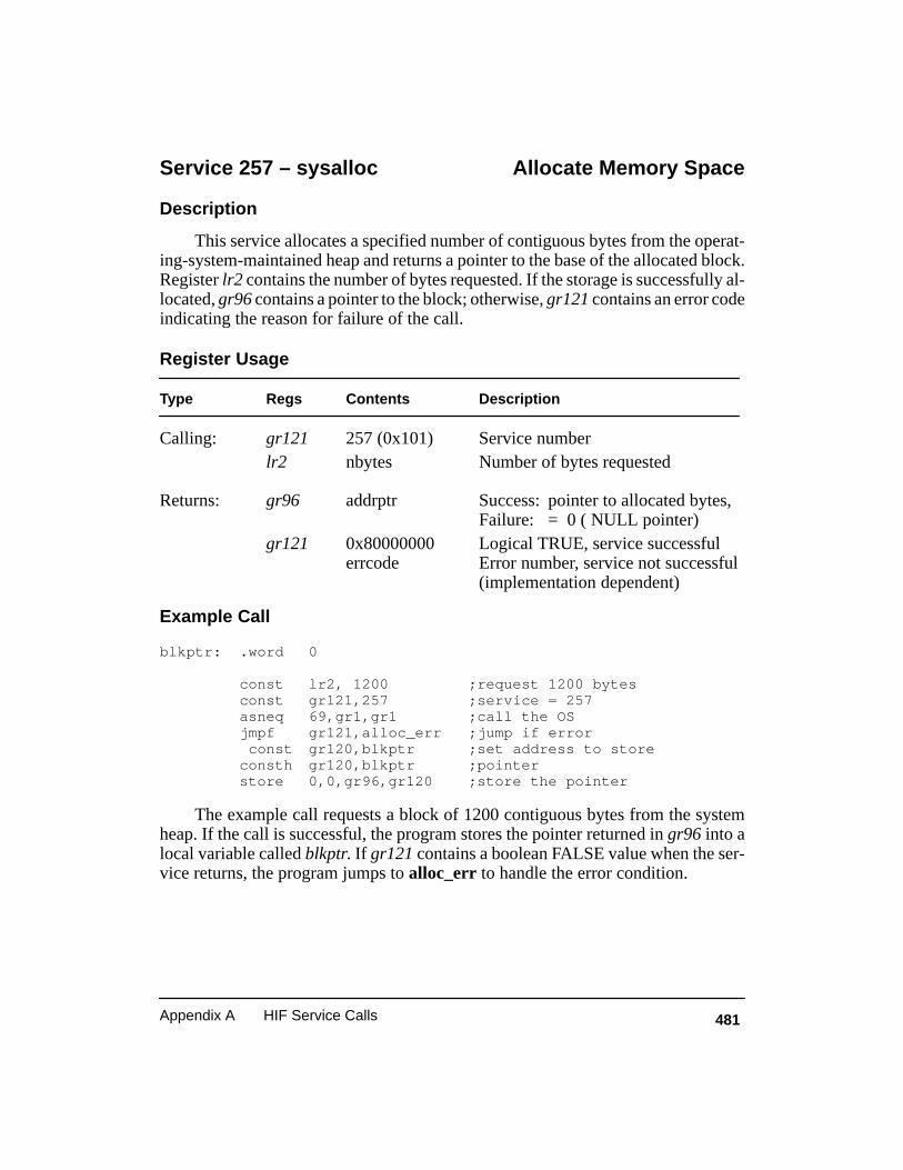
481Appendix A HIF Service Calls
Service 257 – sysalloc Allocate Memory Space
Description
This service allocates a specified number of contiguous bytes from the operat-ing-system-maintained heap and returns a pointer to the base of the allocated block.Register lr2 contains the number of bytes requested. If the storage is successfully al-located, gr96 contains a pointer to the block; otherwise, gr121 contains an error codeindicating the reason for failure of the call.
Register Usage
Type Regs Contents Description
Calling: gr121 257 (0x101) Service numberlr2 nbytes Number of bytes requested
Returns: gr96 addrptr Success: pointer to allocated bytes,
Failure: = 0 ( NULL pointer)gr121 0x80000000 Logical TRUE, service successful
errcode Error number, service not successful (implementation dependent)
Example Call
blkptr: .word 0
const lr2, 1200 ;request 1200 bytesconst gr121,257 ;service = 257asneq 69,gr1,gr1 ;call the OSjmpf gr121,alloc_err ;jump if error const gr120,blkptr ;set address to storeconsth gr120,blkptr ;pointerstore 0,0,gr96,gr120 ;store the pointer
The example call requests a block of 1200 contiguous bytes from the systemheap. If the call is successful, the program stores the pointer returned in gr96 into alocal variable called blkptr. If gr121 contains a boolean FALSE value when the ser-vice returns, the program jumps to alloc_err to handle the error condition.
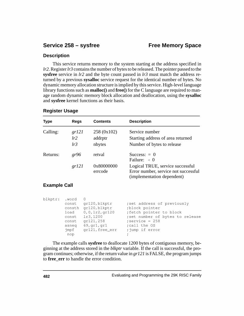
482 Evaluating and Programming the 29K RISC Family
Service 258 – sysfree Free Memory Space
Description
This service returns memory to the system starting at the address specified inlr2. Register lr3 contains the number of bytes to be released. The pointer passed to thesysfree service in lr2 and the byte count passed in lr3 must match the address re-turned by a previous sysalloc service request for the identical number of bytes. Nodynamic memory allocation structure is implied by this service. High-level languagelibrary functions such as malloc() and free() for the C language are required to man-age random dynamic memory block allocation and deallocation, using the sysallocand sysfree kernel functions as their basis.
Register Usage
Type Regs Contents Description
Calling: gr121 258 (0x102) Service numberlr2 addrptr Starting address of area returnedlr3 nbytes Number of bytes to release
Returns: gr96 retval Success: = 0
Failure: < 0gr121 0x80000000 Logical TRUE, service successful
errcode Error number, service not successful (implementation dependent)
Example Call
blkptr: .word 0const gr120,blkptr ;set address of previouslyconsth gr120,blkptr ;block pointerload 0,0,lr2,gr120 ;fetch pointer to blockconst lr3,1200 ;set number of bytes to releaseconst gr121,258 ;service = 258asneq 69,gr1,gr1 ;call the OSjmpf gr121,free_err ;jump if error nop ;
The example calls sysfree to deallocate 1200 bytes of contiguous memory, be-ginning at the address stored in the blkptr variable. If the call is successful, the pro-gram continues; otherwise, if the return value in gr121 is FALSE, the program jumpsto free_err to handle the error condition.

483Appendix A HIF Service Calls
Service 259 – getpsize Return Memory Page Size
Description
This service returns, in register gr96, the page size, in bytes, used by the memorysystem of the HIF implementation.
Register Usage
Type Regs Contents Description
Calling: gr121 259 (0x103) Service number Returns: gr96 pagesize Success: memory page size, one of
the following: 1024,2048,4096,8192Failure: < 0
gr121 0x80000000 Logical TRUE, service successfulerrcode Error number, service not successful
(implementation dependent)
Example Call
pagsiz: .word 0
const gr121,259 ;service = 259asneq 69,gr1,gr1 ;call the OSjmpf gr121,pag_err ;jump if error const gr120,pagsiz ;set address toconsth gr120,pagsiz ;store the page sizestore 0,0,gr96,gr120 ;store it!
The example calls the operating system kernel to return the page size used by thevirtual memory system. If the call was successful, gr121 will contain a booleanTRUE result and the program will store the value in gr96 into the pagsiz variable;otherwise, a boolean FALSE is returned in gr121. In this case, the program will jumpto pag_err to handle the error condition.

484 Evaluating and Programming the 29K RISC Family
Service 260 – getargs Return Base Address
Description
This service returns the base address of the command-line-argument vector,argv, in register gr96, as constructed by the operating system kernel when an applica-tion program is invoked.
Arguments are stored by the operating system as a series of NULL-terminatedcharacter strings. A pointer containing the address of each string is stored in an arraywhose base address (referred to as argv) is returned by the getargs HIF service. Thelast entry in the array contains a NULL pointer (an address consisting of all zero bits).The number of arguments can be computed by counting the number of pointers in thearray, using the fact that the NULL pointer terminates the list.
Register Usage
Type Regs Contents Description
Calling: gr121 260 (0x104) Service number Returns: gr96 baseaddr Success: base address of argv
Failure: = 0 ( NULL pointer)gr121 0x80000000 Logical TRUE, service successful
errcode Error number, service not successful (implementation dependent)
Example Call
argptr: .word 0const gr121,260 ;service = 260asneq 69,gr1,gr1 ;call the OSjmpf gr121,bas_err ;jump if error const gr120,argptr ;set address where baseconsth gr120,argptr ;pointer is to be storedstore 0,0,gr96,gr120 ;store the pointer
The example calls operating system service 260 to access the command-line-ar-gument vector address. If the service executes without error, the program continuesby storing the argument vector address in the variable basptr. If gr121 contains aboolean FALSE value upon return, the program jumps to bas_err to handle the errorcondition.
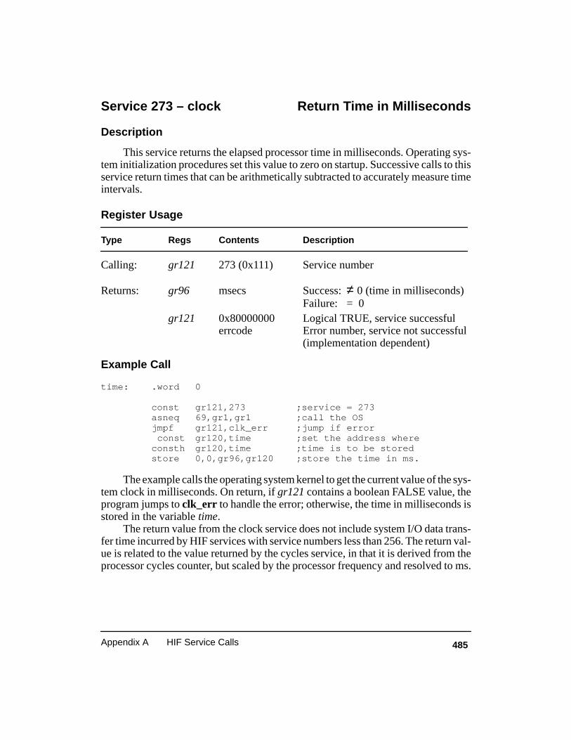
485Appendix A HIF Service Calls
Service 273 – clock Return Time in Milliseconds
Description
This service returns the elapsed processor time in milliseconds. Operating sys-tem initialization procedures set this value to zero on startup. Successive calls to thisservice return times that can be arithmetically subtracted to accurately measure timeintervals.
Register Usage
Type Regs Contents Description
Calling: gr121 273 (0x111) Service number Returns: gr96 msecs Success:≠ 0 (time in milliseconds)
Failure: = 0gr121 0x80000000 Logical TRUE, service successful
errcode Error number, service not successful (implementation dependent)
Example Call
time: .word 0
const gr121,273 ;service = 273asneq 69,gr1,gr1 ;call the OSjmpf gr121,clk_err ;jump if error const gr120,time ;set the address whereconsth gr120,time ;time is to be storedstore 0,0,gr96,gr120 ;store the time in ms.
The example calls the operating system kernel to get the current value of the sys-tem clock in milliseconds. On return, if gr121 contains a boolean FALSE value, theprogram jumps to clk_err to handle the error; otherwise, the time in milliseconds isstored in the variable time.
The return value from the clock service does not include system I/O data trans-fer time incurred by HIF services with service numbers less than 256. The return val-ue is related to the value returned by the cycles service, in that it is derived from theprocessor cycles counter, but scaled by the processor frequency and resolved to ms.
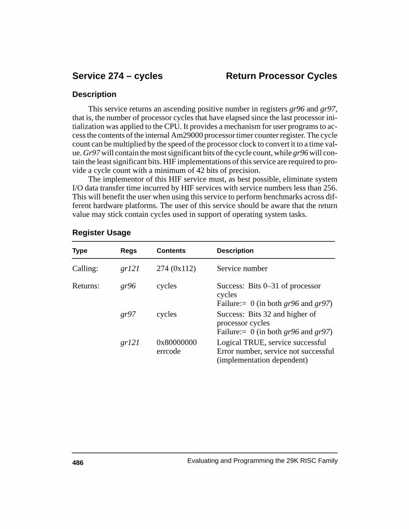
486 Evaluating and Programming the 29K RISC Family
Service 274 – cycles Return Processor Cycles
Description
This service returns an ascending positive number in registers gr96 and gr97,that is, the number of processor cycles that have elapsed since the last processor ini-tialization was applied to the CPU. It provides a mechanism for user programs to ac-cess the contents of the internal Am29000 processor timer counter register. The cyclecount can be multiplied by the speed of the processor clock to convert it to a time val-ue. Gr97 will contain the most significant bits of the cycle count, while gr96 will con-tain the least significant bits. HIF implementations of this service are required to pro-vide a cycle count with a minimum of 42 bits of precision.
The implementor of this HIF service must, as best possible, eliminate systemI/O data transfer time incurred by HIF services with service numbers less than 256.This will benefit the user when using this service to perform benchmarks across dif-ferent hardware platforms. The user of this service should be aware that the returnvalue may stick contain cycles used in support of operating system tasks.
Register Usage
Type Regs Contents Description
Calling: gr121 274 (0x112) Service number Returns: gr96 cycles Success: Bits 0–31 of processor
cycles Failure:= 0 (in both gr96 and gr97)
gr97 cycles Success: Bits 32 and higher of processor cycles Failure:= 0 (in both gr96 and gr97)
gr121 0x80000000 Logical TRUE, service successful errcode Error number, service not successful
(implementation dependent)
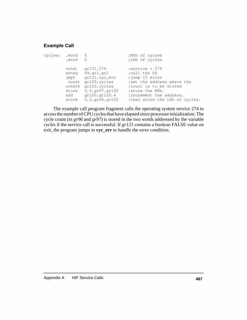
487Appendix A HIF Service Calls
Example Call
cycles: .word 0 ;MSb of cycles.word 0 ;LSb of cycles
const gr121,274 ;service = 274asneq 69,gr1,gr1 ;call the OSjmpf gr121,cyc_err ;jump if error const gr120,cycles ;set the address where theconsth gr120,cycles ;count is to be storedstore 0,0,gr97,gr120 ;store the MSb,add gr120,gr120,4 ;increment the address,store 0,0,gr96,gr120 ;then store the LSb of cycles.
The example call program fragment calls the operating system service 274 toaccess the number of CPU cycles that have elapsed since processor initialization. Thecycle count (in gr96 and gr97) is stored in the two words addressed by the variablecycles if the service call is successful. If gr121 contains a boolean FALSE value onexit, the program jumps to cyc_err to handle the error condition.
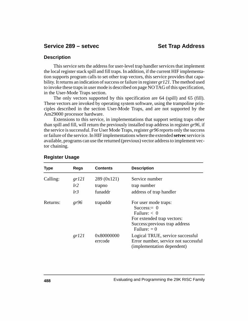
488 Evaluating and Programming the 29K RISC Family
Service 289 – setvec Set Trap Address
Description
This service sets the address for user-level trap handler services that implementthe local register stack spill and fill traps. In addition, if the current HIF implementa-tion supports program calls to set other trap vectors, this service provides that capa-bility. It returns an indication of success or failure in register gr121. The method usedto invoke these traps in user mode is described on page NO TAG of this specification,in the User-Mode Traps section.
The only vectors supported by this specification are 64 (spill) and 65 (fill).These vectors are invoked by operating system software, using the trampoline prin-ciples described in the section User-Mode Traps, and are not supported by theAm29000 processor hardware.
Extensions to this service, in implementations that support setting traps otherthan spill and fill, will return the previously installed trap address in register gr96, ifthe service is successful. For User Mode Traps, register gr96 reports only the successor failure of the service. In HIF implementations where the extended setvec service isavailable, programs can use the returned (previous) vector address to implement vec-tor chaining.
Register Usage
Type Regs Contents Description
Calling: gr121 289 (0x121) Service numberlr2 trapno trap numberlr3 funaddr address of trap handler
Returns: gr96 trapaddr For user mode traps:
Success:= 0 Failure: < 0 For extended trap vectors:Success:previous trap address Failure: = 0
gr121 0x80000000 Logical TRUE, service successful errcode Error number, service not successful
(implementation dependent)
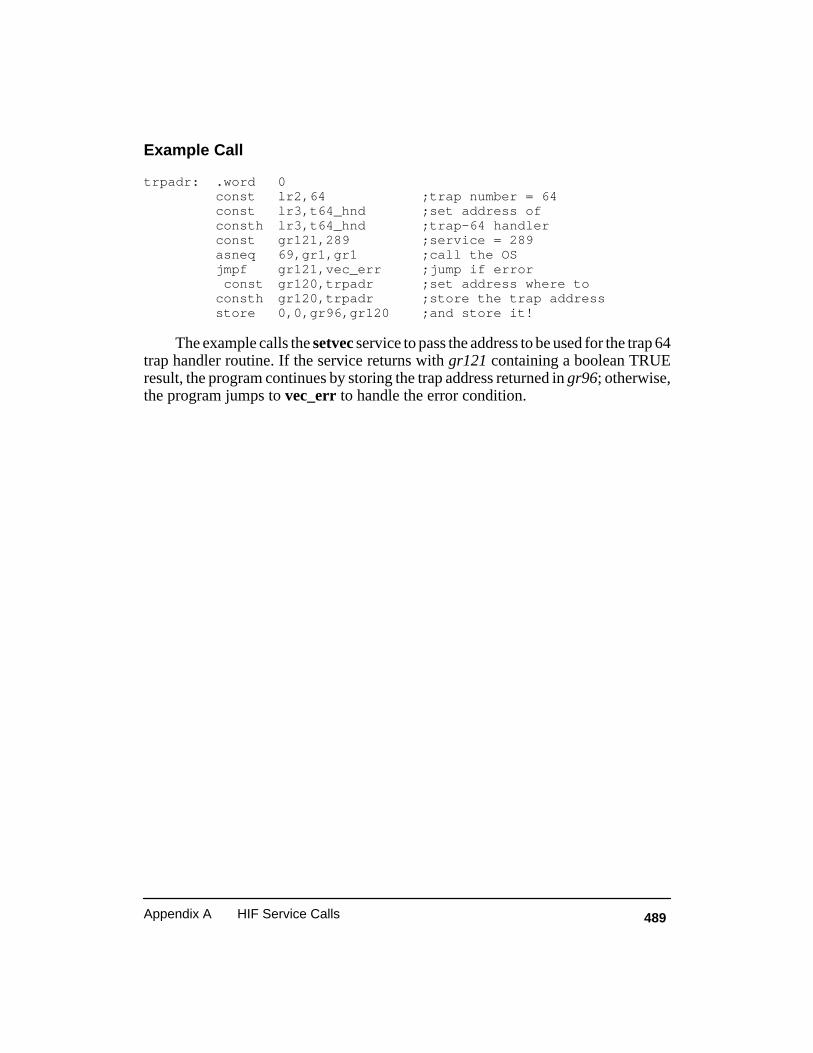
489Appendix A HIF Service Calls
Example Call
trpadr: .word 0const lr2,64 ;trap number = 64const lr3,t64_hnd ;set address ofconsth lr3,t64_hnd ;trap-64 handlerconst gr121,289 ;service = 289asneq 69,gr1,gr1 ;call the OSjmpf gr121,vec_err ;jump if error const gr120,trpadr ;set address where toconsth gr120,trpadr ;store the trap addressstore 0,0,gr96,gr120 ;and store it!
The example calls the setvec service to pass the address to be used for the trap 64trap handler routine. If the service returns with gr121 containing a boolean TRUEresult, the program continues by storing the trap address returned in gr96; otherwise,the program jumps to vec_err to handle the error condition.
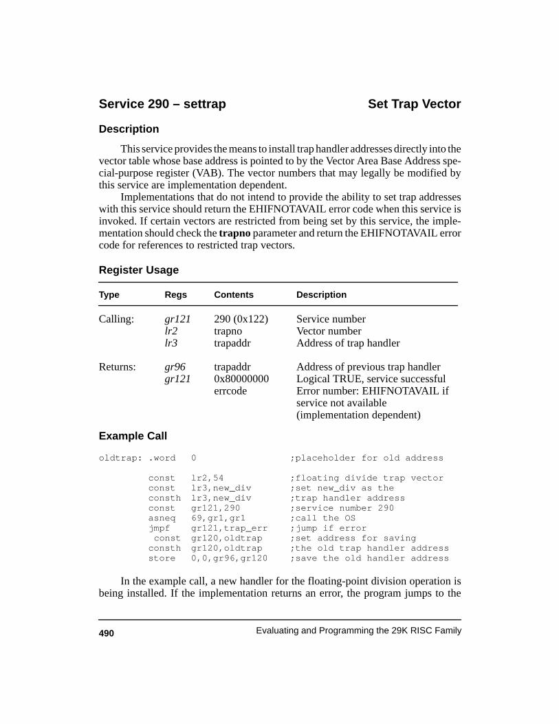
490 Evaluating and Programming the 29K RISC Family
Service 290 – settrap Set Trap Vector
Description
This service provides the means to install trap handler addresses directly into thevector table whose base address is pointed to by the Vector Area Base Address spe-cial-purpose register (VAB). The vector numbers that may legally be modified bythis service are implementation dependent.
Implementations that do not intend to provide the ability to set trap addresseswith this service should return the EHIFNOTAVAIL error code when this service isinvoked. If certain vectors are restricted from being set by this service, the imple-mentation should check the trapno parameter and return the EHIFNOTAVAIL errorcode for references to restricted trap vectors.
Register Usage
Type Regs Contents Description
Calling: gr121 290 (0x122) Service numberlr2 trapno Vector numberlr3 trapaddr Address of trap handler
Returns: gr96 trapaddr Address of previous trap handler
gr121 0x80000000 Logical TRUE, service successful errcode Error number: EHIFNOTAVAIL if
service not available(implementation dependent)
Example Call
oldtrap: .word 0 ;placeholder for old address
const lr2,54 ;floating divide trap vectorconst lr3,new_div ;set new_div as theconsth lr3,new_div ;trap handler addressconst gr121,290 ;service number 290asneq 69,gr1,gr1 ;call the OSjmpf gr121,trap_err ;jump if error const gr120,oldtrap ;set address for savingconsth gr120,oldtrap ;the old trap handler addressstore 0,0,gr96,gr120 ;save the old handler address
In the example call, a new handler for the floating-point division operation isbeing installed. If the implementation returns an error, the program jumps to the
491Appendix A HIF Service Calls
trap_err label. If the service was successful and a new trap handler was installed, theprevious handler address (if any) is stored into the oldtrap variable.
There is often a need for programs operating on dedicated hardware to enter su-pervisor mode. This can be accomplished by reserving a trap vector for that purposeand installing a trap handler routine to return control to the user in supervisor mode.The operation is effected by issuing an assert instruction that invokes the specifiedtrap. User mode can be restored by clearing (setting to 0) the Supervisor Mode bit (4)of the Current Processor Status register (CPS).

492 Evaluating and Programming the 29K RISC Family
Service 291 – setim Set Interrupt Mask
Description
This service provides the means to set the interrupt mask (IM) field and the dis-able interrupts (DI) field of the current processor status register (CPS). This field en-ables the external interrupt pins INTR0–INTR3, according to the following encod-ing:
00 INTR0 enabled01 INTR1–INTR0 enabled10 INTR2–INTR0 enabled11 INTR3–INTR0 enabled
These two bits provide for a priority-oriented enabling capability; however, theINTR0 interrupt can not be disabled through the IM field alone. The disable inter-rupts (di ) parameter must be set to 1 to produce this effect. A di value of 0 will en-able the selected interrupts, and a value of 2 will leave the DI-bit of the CPS un-changed. If this service is not implemented, an error code of EHIFNOTAVAILshould be returned by the software. The error code for an illegal value in registers lr2or lr3 is implementation dependent.
Register Usage
Type Regs Contents Description
Calling: gr121 291 (0x123) Service numberlr2 mask New mask field valuelr3 di 0= Enable interrupts
1= Disable interrupts2= Leave interrupt enable unchanged
Returns: gr96 mask Old mask field value
gr121 0x80000000 Logical TRUE, service successful errcode Error number: EHIFNOTAVAIL if
service not available(implementation dependent)
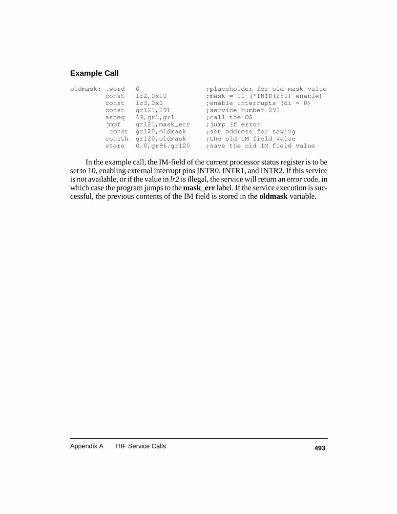
493Appendix A HIF Service Calls
Example Call
oldmask: .word 0 ;placeholder for old mask valueconst lr2,0x10 ;mask = 10 (*INTR(2:0) enable)const lr3,0x0 ;enable interrupts (di = 0)const gr121,291 ;service number 291asneq 69,gr1,gr1 ;call the OSjmpf gr121,mask_err ;jump if error const gr120,oldmask ;set address for savingconsth gr120,oldmask ;the old IM field valuestore 0,0,gr96,gr120 ;save the old IM field value
In the example call, the IM-field of the current processor status register is to beset to 10, enabling external interrupt pins INTR0, INTR1, and INTR2. If this serviceis not available, or if the value in lr2 is illegal, the service will return an error code, inwhich case the program jumps to the mask_err label. If the service execution is suc-cessful, the previous contents of the IM field is stored in the oldmask variable.

494 Evaluating and Programming the 29K RISC Family
Service 305 – query Return Version Information
Description
This service returns version information, or capabilities of the HIF implementa-tion, as requested. On entry, the requested capability is passed as an argument in lr2.The service returns the requested information, or indicates that it is unavailable, ingr96.
Register Usage
Type Regs Contents Description
Calling: gr121 305 (0x131) Service numberlr2 capcode Capabilities code
0 = Request HIF version1 = Request CPU version & family code2 = Request Am29027 arithmetic accelerator version3 = Request CPU clock frequency4 = Request memory environment
For lr2 = 0 (HIF version)Returns: gr96 hifvers Success:≥ 0 (encoded version
information). The version numberis returned as two 4-bit fields in the low-order 8 bits of the return value. The two fields are separated by animplied decimal point (e.g., 0x20 means HIF V2.0).Failure: < 0 (or unavailable)
For lr2 = 1 (CPU version and family code)Returns: gr96 cpuvers Success:≥ 0 (encoded
version/family).The high-order 8 bitsof the configuration register (CFG), known as the processor release level (PRL) are moved to the low-order 8 bits of gr96, as two 4-bit fields.Failure: < 0 (or unavailable)
For lr2 = 2 (Am29027 coprocessor version)

495Appendix A HIF Service Calls
Returns: gr96 027vers Success:≥ 0 (encoded version information). The high-order 8 bitsof the accelerator’s precision registerform the arithmetic accelerator release level (ARL) and are moved to the low-order 8 bits of gr96, as two 4-bit fields.Failure: < 0 (or unavailable)
For lr2 = 3 (CPU clock frequency)Returns: gr96 clkfreq Success: > 0 (frequency in Hertz)
Failure: = 0 (or unavailable)For lr2 = 4 (Memory environment)
gr96 memenv Success: > 0 (memory environment)BYTEW 0x1 byte-write availableDWSET 0x2DW-bit setIREAD 0x4 Instruction memory readableFailure: ≤ 0 (or unavailable)
For all requestsReturns: gr121 0x80000000 Logical TRUE, service successful
errcode error number, service not successful(implementation dependent)
In addition to the Return Usage table requests, negative capcode values in regis-ter lr2 are available for implementation-dependent encoding of query requests. Allpositive values in register lr2 are reserved for future expansion of the HIF query ser-vice.
Example Call
vers: .word 0const lr2,0 ;request HIF versionconst gr121,305 ;service = 305asneq 69,gr1,gr1 ;call the OSjmpf gr121,qry_err ;handle query error const lr2,vers ;address to store version infoconsth lr2,versstore 0,0,gr96,lr2 ;store the HIF version number
In the example call, a request code of 0 is loaded into lr2 and the service is called.Upon return, if the value in gr121 is FALSE, indicating failure, the program jumps toan error routine. If gr121 is TRUE, then the program stores the returned HIF versioninformation into the variable called vers.

496 Evaluating and Programming the 29K RISC Family
Service 321 – signal Register Signal Handler
Description
This service provides the means to register (or un-register) a specified user sig-nal handler. Local register lr2 contains the address of the user signal handler routineon entry. This routine is expected to handle the signals shown in Table A-2, below.Sections 2.5, 4.4 and Appendix B, contain additional information on writing signalhandlers for complex environments.
The HIF service returns the address of the previously installed handler in gr96.If no previous handler was installed, gr96 will contain a NULL pointer (gr96 = 0).Signal handlers may perform any appropriate processing, but only the services withservice numbers above 256 are guaranteed to be available. Calls to services withnumbers below 256 may result in unpredictable behavior when returning to the inter-rupted program—unless the service executes a longjump(), which avoids executionof the interrupt return service (see Table A-3).
To un-register a signal handler, local register lr2 must contain a value of 0(NULL) on entry. When a handler is un-registered in this manner, signal handlingwill revert to the default behavior established by the operating system.
When one of the (SIGINT or SIGFPE) signals occurs, the HIF implementationmust preserve: the signal number that occurred; the register stack pointer (gr1); theregister allocate bounds (gr126); the program counters, PC0–PC2; the channel regis-ters (CHA, CHD, and CHC ); the ALU register; the old processor status, OPS; and thecontents of gr121. These registers are saved in the user memory stack. The HIF im-plementation must be careful not to disturb values in registers that have not beensaved on the user’s stack. Global register gr125 should contain the address of the lastsaved value in the HIF Signal Stack (e.g., gr121) at the conclusion of this phase.Figure A-1 illustrates the required user stack format for saved registers.
Table A-2. Default Signals Handled by HIF
Mnemonic Value Description
SIGINT 2 User interrupt (e.g., from keyboard)SIGFPE 8 Floating–point exception

497Appendix A HIF Service Calls
gr125 points to thelast register savedby the HIF in the user’s stack.
Figure A-1. HIF Register Preservation for Signals
User’sStack
signal numberHigher Addresses
Lower Addresses
gr1
gr126
PC0
PC1
PC2
CHA
CHD
CHC
ALU
OPS
gr121
Registers Saved by HIF
(rab)
(tav)
It is at this point that execution of the HIF invokes the handler specified by thenewsig parameter to the signal service. The handler is invoked with the processormode set to the mode of the interrupted program (either user or supervisor). Depend-ing on the nature of the interrupt (SIGINT or SIGFPE) and the complexity of the han-dler, additional registers may need to be saved. In this case, the handler must pre-serve: the values in the indirect pointers IPA, IPB, and IPC; the contents of the Q reg-ister; the stack frame pointer, lr1; and the local register stack free bounds in rfb(gr127). In addition, because high-level languages use global registers gr96–gr124as temporaries, the user signal handler may have to save these as well.
User signal handlers can be grouped into three levels of complexity, dependingon the implementation:
1. The least complex are handlers which have no intention of returning controlto the user. In this case, only a few additional registers may need to be saved(if any).
2. Floating-point error handlers are often more complex, where some of theuser’s context needs to be saved. In this case, probably only the indirect point-ers (IPA–IPC), the Q register, and gr125 need be preserved. After the errorhas been handled, the handler will issue one of the signal return services listedin Table A-3 to return control to the user’s program.
3. The most complex handlers will be those that need to return to the user pro-gram at the C-level of context. If the handler intends to pass control to a user-

498 Evaluating and Programming the 29K RISC Family
provided signal routine (e.g., to handle SIGINT), then it may be necessary topreserve all of the registers indicated in the figure above. In addition, han-dlers that intend to return control at the C-level of context will need to makeprovision for completing any interrupted SPILL or FILL operations or com-plete a long-jump that may be in progress. Fortunately, AMD supplies thenecessary code in library routines supplied with most tool products (see Ap-pendix B).
Before execution of the signal handler, the HIF conforming operating system isresponsible for clearing the Channel Control (CHC) register (setting it to 0), to pre-vent restarting a load or store multiple operation that may have been interrupted. Theproper contents of this register will be restored by the HIF when the handler issuesone of the service requests listed in Table A-3.
Once a signal handler is invoked by one of the signals listed in Table A-2, andwhen it has finished, it will usually return to the operating system by invoking one ofthe signal return services shown in Table A-3, below, with register gr125 pointing tothe last saved register in the HIF-saved-registers (i.e., gr121), as shown in Fig-ure A–1. More complex implementations may make other arrangements for return-ing to the user program’s context. Sample code for saving and restoring the necessaryregisters is shown in section 4.4 and Appendix B.
The handler is responsible for determining the appropriate action for each typeof interrupt (SIGINT or SIGFPE), and must return control to the operating systemusing one of the services listed in Table A-3, after first restoring the indirect pointers(IPA–IPC), the Q register, and with gr125 pointing to the last saved register in theuser’s stack (assuming the suggested approach for preserving registers is followed).
Table A-3. HIF Signal Return Services
Service Name Description
322 sigdfl Perform default signal handling323 sigret Return to location indicated by PC1324 sigrep Return to location indicated by PC2325 sigskp Return to location indicated by PC0
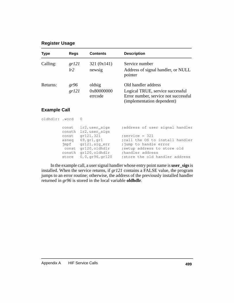
499Appendix A HIF Service Calls
Register Usage
Type Regs Contents Description
Calling: gr121 321 (0x141) Service numberlr2 newsig Address of signal handler, or NULL
pointer
Returns: gr96 oldsig Old handler addressgr121 0x80000000 Logical TRUE, service successful
errcode Error number, service not successful(implementation dependent)
Example Call
oldhdlr: .word 0
const lr2,user_sigs ;address of user signal handlerconsth lr2,user_sigsconst gr121,321 ;service = 321asneq 69,gr1,gr1 ;call the OS to install handlerjmpf gr121,sig_err ;jump to handle error const gr120,oldhdlr ;setup address to store oldconsth gr120,oldhdlr ;handler addressstore 0,0,gr96,gr120 ;store the old handler address
In the example call, a user signal handler whose entry point name is user_sigs isinstalled. When the service returns, if gr121 contains a FALSE value, the programjumps to an error routine; otherwise, the address of the previously installed handlerreturned in gr96 is stored in the local variable oldhdlr .

500 Evaluating and Programming the 29K RISC Family
Service 322 – sigdfl Perform Default Signal Action
Description
This service is called only from within a user signal handler installed using thesignal (321) service. The function of this service is to instruct the HIF to perform thepredetermined default action for the specified signal. The operating system is re-sponsible for establishing the appropriate default action.
Register Usage
Type Regs Contents Description
Calling: gr121 322 (0x142) Service numbergr125 sigptr Pointer to HIF Signal Stack
containing preserved registers(See signal (321) for further information.)
Returns: Does not return
Example Call
const gr121,322 ;service = 322asneq 69,gr1,gr1 ;call the OS
Since this service does not return, no attempt is made to test returned values orstore results.

501Appendix A HIF Service Calls
Service 323 – sigret Return From Signal Interrupt
Description
This service is called only from within a user signal handler installed using thesignal (321) service. The function of this service is to return from the latest signalinterrupt, to the location specified by the value in program counter PC1 at the time thesignal occurred. Once invoked, this service does not return to the user signal handler.
Register Usage
Type Regs Contents Description
Calling: gr121 323 (0x143) Service numbergr125 sigptr Pointer to HIF Signal Stack
containing preserved registers(See signal (321) for further information.)
Returns: Does not return
Example Call
const gr121,323 ;service = 323asneq 69,gr1,gr1 ;call the OS
Since this service does not return, no attempt is made to test returned values orstore results.

502 Evaluating and Programming the 29K RISC Family
Service 324 – sigrep Return From Signal Interrupt
Description
This service is called only from within a user signal handler installed using thesignal (321) service. The function of this service is to return from the latest signalinterrupt to the location specified by the value in program counter PC2 at the time thesignal occurred. Once invoked, this service does not return to the user signal handler.
Register Usage
Type Regs Contents Description
Calling: gr121 324 (0x144) Service numbergr125 sigptr Pointer to HIF Signal Stack
containing preserved registers(See signal (321) for further information.)
Returns: Does not return
Example Call
const gr121,324 ;service = 324asneq 69,gr1,gr1 ;call the OS
Since this service does not return, no attempt is made to test returned values orstore results.

503Appendix A HIF Service Calls
Service 325 – sigskp Return From Signal Interrupt
Description
This service is called only from within a user signal handler installed using thesignal (321) service. The function of this service is to return from the latest signalinterrupt to the location specified by the value in program counter PC0 at the time thesignal occurred. Once invoked, this service does not return to the user signal handler.
Register Usage
Type Regs Contents Description
Calling: gr121 325 (0x145) Service numbergr125 sigptr Pointer to HIF Signal Stack
containing preserved registers(See signal (321) for further information.)
Returns: Does not return
Example Call
const gr121,325 ;service = 325asneq 69,gr1,gr1 ;call the OS
Since this service does not return, no attempt is made to test returned values orstore results.

504 Evaluating and Programming the 29K RISC Family
Service 326 – sendsig Send Signal
Description
This service provides the means to send a signal to the current process, to sup-port signal testing. A single parameter, sig, specifies the signal number to be sent.
Register Usage
Type Regs Contents Description
Calling: gr121 326 (0x141) Service numberlr2 sig Signal number to be sent to current
process
Returns: gr121 0x80000000 Logical TRUE, service successfulerrcode Error number, service not successful
EHIFNOTAVAIL if service not implemented.(implementation dependent)
Example Call
const lr2,SIGFPE ;floating-point exceptionconst gr121,326 ;service = 326asneq 69,gr1,gr1 ;call the OSjmpf gr121,send_err ;handle signaling error nop
In the above example, a floating-point exception error signal is being sent to thecurrent process. It is presumed that a signal handler for the SIGFPE (floating-pointexception) error has been previously installed (see signal service) and is being tested.

505Appendix A HIF Service Calls
A.2 Error Numbers
HIF implementations are required to return error codes when a requested opera-tion is not possible. The codes from 0–10,000 are reserved for compatibility withcurrent and future error return standards. The currently assigned codes and theirmeanings are shown in Tables A–4 through A–9. If a HIF implementation returns anerror code in the range of 0–10,000, it must carry the identical meaning to the corre-sponding error code in this table. Error code values larger than 10,000 are availablefor implementation-specific errors.
Table A-4. HIF Error Numbers Assigned
Number Name Description
0 Not used.
1 EPERM Not owner
This error indicates an attempt to modify a file in some way forbiddenexcept to its owner.
2 ENOENT No such file or directory
This error occurs when a file name is specified and the file should exist but does not, or when one of the directories in a pathname does not exist.
3 ESRCH No such process
The process or process group whose number was given does not exist, or any such process is already dead.
4 EINTR Interrupted system call
This error indicates that an asynchronous signal (such as interrupt or quit) that the user has elected to catch occurred during a system call.
5 EIO I/O error
Some physical I/O error occurred during a read or write. This error may in some cases occur on a call following the one to which it actually applies.
6 ENXIO No such device or address
I/O on a special file refers to a sub-device that does not exist or is beyond the limits of the device.
7 E2BIG Arg list is too long
An argument list longer than 5120 bytes is presented to executive.
8 ENOEXEC Exec format error
A request is made to execute a file that, although it has the appropriate permissions, does not start with a valid magic number.
9 EBADF Bad file number
Either a file descriptor refers to no open file, or a read (write) request is made to a file that is open only for writing (reading).

506 Evaluating and Programming the 29K RISC Family
Table A-5. HIF Error Numbers Assigned (continued)
Number Name Description
10 ECHILD No children
Wait and the process has no living or unwaited for children.
11 EAGAIN No more processes
In a fork, the system’s process table is full, or the user is not allowed to create any more processes.
12 ENOMEM Not enough memory
During an executive or break, a program asks for more memory than thesystem is able to supply or else a process size limit would be exceeded.
13 EACCESS Permission denied
An attempt was made to access a file in a way forbidden by the protectionsystem.
14 EFAULT Bad address
The system encountered a hardware fault in attempting to access thearguments of a system call.
15 ENOTBLK Block device required
A plain file was mentioned where a block device was required, such as in mount.
16 EBUSY Device busy
An attempt was made to mount a device that was already mounted, or an attempt was made to dismount a device on which there is an active file (open file, current directory, mounted-on file, or active text segment).
17 EEXIST File exists
An existing file was mentioned in an inappropriate context (e.g., link).
18 EXDEV Cross-device link
A hard link to a file on another device was attempted.
19 ENODEV No such device
An attempt was made to apply an inappropriate system call to a device, for example, to read a write-only device, or the device is not configured by the system.
20 ENOTDIR Not a directory
A non-directory was specified where a directory is required, for example, in a path name or as an argument to chdir.
21 EISDIR Is a directory
An attempt to write on a directory.

507Appendix A HIF Service Calls
Table A-6. HIF Error Numbers Assigned (continued)
Number Name Description
22 EINVAL Invalid argument
This error occurs when some invalid argument for the call is specified. For example, dismounting a non-mounted device, mentioning an unknown signal in signal, or specifying some other argument that is inappropriate forthe call.
23 ENFILE File table overflow
The system’s table of open files is full, and temporarily no more open requests can be accepted.
24 EMFILE Too many open files
The configuration limit on the number of simultaneously open files has been exceeded.
25 ENOTTY Not a typewriter
The file mentioned in stty or gtty is not a terminal or one of the otherdevices to which these calls apply.
26 ETXTBSY Text file busy
The referenced text file is busy and the current request can not be honored.
27 EFBIG File too large
The size of a file exceeded the maximum limit.
28 ENOSPC No space left on device
A write to an ordinary file, the creation of a directory or symbolic link, or the creation of a directory entry failed because no more disk blocks are available on the file system.
29 ESPIPE Illegal seek
A seek was issued to a socket or pipe. This error may also be issued for other non-seekable devices.
30 EROFS Read-only file system
An attempt to modify a file or directory was made on a device mounted read-only.
31 EMLINK Too many links
An attempt was made to establish a new link to the requested file and the limit of simultaneous links has been exceeded.
32 EPIPE Broken pipe
A write on a pipe or socket was attempted for which there is no process to read the data. This condition normally generates a signal; the error is returned if the signal is caught or ignored.
33 EDOM Argument too large
The argument of a function in the math package is out of the domain of the function.

508 Evaluating and Programming the 29K RISC Family
Table A-7. HIF Error Numbers Assigned (continued)
Number Name Description
34 ERANGE Result too large
The value of a function in the math package is unrepresentable withinmachine precision.
35 EWOULDBLOCK Operation would block
An operation that would cause a process to block was attempted on an object in non-blocking mode.
36 EINPROGRESS Operation now in progress
An operation that takes a long time to complete was attempted on a non-blocking object.
37 EALREADY Operation already in progress
An operation was attempted on a non-blocking object that already had anoperation in progress.
38 ENOTSOCK Socket-operation on non-socket
A socket oriented operation was attempted on a non-socket device.
39 EDESTADDRREQDestination address required
A required address was omitted from an operation on a socket.
40 EMSGSIZE Message too long
A message sent on a socket was larger than the internal message buffer or some other network limit.
41 EPROTOTYPE Protocol wrong type for socket
A protocol was specified that does not support the semantics of the socket type requested.
42 ENOPROTOOPT Option not supported by protocol
A bad option or level was specified when accessing socket options.
43 EPROTONOSUPPORTProtocol not supported
The protocol has not been configured into the system, or no implementation for it exists.
44 ESOCKTNOSUPPORTSocket type not supported
The support for the socket type has not been configured into the system, or no implementation for it exists.
45 EOPNOTSUPP Operation not supported on socket
For example, trying to accept a connection on a datagram socket.
46 EPFNOSUPPORTProtocol family not supported
The protocol family has not been configured into the system or no implementation for it exists.

509Appendix A HIF Service Calls
Table A-8. HIF Error Numbers Assigned (continued)
Number Name Description
47 EAFNOSUPPORTAddress family not supported by protocol family
An address was used that is incompatible with the requested protocol.
48 EADDRINUSE Address already in use
Only one usage of each address is normally permitted.
49 EADDRNOTAVAILCannot assign requested address
This normally results from an attempt to create a socket with an address not on this machine.
50 ENETDOWN Network is down
A socket operation encountered a dead network.
51 ENETUNREACH Network is unreachable
A socket operation was attempted to an unreachable network.
52 ENETRESET Network dropped connection on reset
The host you were connected to crashed and rebooted.
53 ECONNABORTEDSoftware caused connection abort
A connection abort was caused internal to your host machine.
54 ECONNRESET Connection reset by peer
A connection was forcibly closed by a peer. This normally results from a loss of the connection on the remote socket due to a timeout or a reboot.
55 ENOBUFS No buffer space available
An operation on a socket or pipe was not performed because the system lacked sufficient buffer space or because a queue was full.
56 EISCONN Socket is already connected
A connect request was made on an already connected socket; or a sendto or sendmsg request on a connected socket specified a destination when already connected.
57 ENOTCONN Socket is not connected
A request to send or receive data was disallowed because the socket was not connected and (when sending on a datagram socket) no address was supplied.
58 ESHUTDOWN Cannot send after socket shutdown
A request to send data was disallowed because the socket had already been shut down with a previous shutdown call.
59 ETOOMANYREFSToo many references; cannot splice.

510 Evaluating and Programming the 29K RISC Family
Table A-9. HIF Error Numbers Assigned (concluded)
Number Name Description
60 ETIMEDOUT Connection timed outA connect or send request failed because the connected party did notproperly respond after a period of time. (The timeout period is dependen on the communication protocol.)
61 ECONNREFUSEDConnection refusedNo connection could be made because the target machine actively refused it. This usually results from trying to connect to a service that is inactive on the foreign host.
62 ELOOP Too many levels of symbolic linksA pathname lookup involved more than the maximum limit of symbolic links.
63 ENAMETOOLONGFile name too longA component of a pathname exceeded the maximum name length, or an entire pathname exceeded the maximum path length.
64 EHOSTDOWN Host is downA socket operation failed because the destination host was down.
65 EHOSTUNREACHHost is unreachableA socket operation was attempted to an unreachable host.
66 ENOTEMPTY Directory not emptyA non-empty directory was supplied to a remove directory or rename call.
67 EPROCLIM Too many processesThe limit of the total number of processes has been reached. No new processes can be created.
68 EUSERS Too many usersThe limit of the total number of users has been reached. No new users may access the system.
69 EDQUOT Disk quota exceededA write to an ordinary file, the creation of a directory or symbolic link, or the creation of a directory entry failed because the user’s quota of disk blocks was exhausted; or the allocation of an inode for a newly created file failed because the user’s quota of inodes was exhausted.
70 EVDBAD RVD related disk error
1001 EHIFNOTAVAIL HIF service not available.The requested HIF service is not implemented or is not available to the user program making the request.
1002 EHIFUNDEF HIF service is undefinedThe HIF service referenced by the program is undefined. No valid HIF service with that service number exists.

511Appendix A HIF Service Calls

512
Appendix B
HIF Signal Processing
B.1 User Trampoline Code
The following 29K assembly language code is a listing of the User mode coderequired to complete signal handler preparation tasks necessary for an HIF compliantoperating system. When address sigcode is reached, the operating system has alreadysaved the portion of the interrupt context frame down to the tav register onto theuser’s memory stack (see section 4.4). This source code is contained in library filesdelivered with the High C 29K product, and is listed here for reference and to aidcomprehension of the way different code fragments fit together in a real implementa-tion.
Implementors who do not wish to use an array of signal handlers, but a singleC–level handler function, can change the code in the call C–level section. They neednot access the SigEntry array to obtain the address of their handler function.
.file ”signal.s”; SigEntry is the address of an array of C–level user code signal; handlers. They must return to the top–level before doing a; sigret() return function. Nested signals are supported.
.externV_SPILL,V_FILL
.extern fill_handler ;In crt0.s
.align 4
.comm WindowSize,4
.data

513Appendix B HIF Signal Processing
.global__SigEntry__SigEntrySigEntry:
.word 0 ;reserved
.word 0 ;adds. of #2 SIGINT handler
.word 0 ;reserved
.word 0 ;reserved
.word 0 ;reserved
.word 0 ;reserved
.word 0 ;reserved
.word 0 ;adds. of #8 SIGFPE handler
.word 0 ;reserved
.word 0 ;reserved
.word 0 ;reserved
.word 0 ;reserved
.word 0 ;reserved
.word 0 ;reserved #14 SIGALARM .rep 29 –14
.word 0 ;reserved .endr
.word 0 ;reserved #30 SIGUSR1
.word 0 ;reserved #31 SIGUSR2
.word 0
;––––––––––––––––––––––––––––––––––––––––––––––––––––––––– Macros .macro push,sp,reg
sub sp,sp,4 ;decrement pointerstore 0,0,reg,sp ;store on stack
.endm; .macro pushsr,sp,reg,sreg
mfsr reg,sreg ;copy from special registersub sp,sp,4 ;decrement pointerstore 0,0,reg,sp ;store on stack
.endm; .macro pop,reg,sp
load 0,0,reg,sp ;get from stackadd sp,sp,4 ;increment pointer
.endm; .macro popsr,sreg,reg,sp
load 0,0,reg,sp ;get from stackadd sp,sp,4 ;increment pointermtsr sreg,reg ;move to special register
.endm
.reg v0,gr96
.reg v1,gr97
514 Evaluating and Programming the 29K RISC Family
.reg v2,gr98
.reg v3,gr99
;================================================= Process Signal; About to deliver a signal to a user mode signal handler.; The state of all the registers (except for msp,chc and rab); is the same as when the process was interrupted.;; We must make the stack and window consistent before calling the; handler. The orignal rab value is on the stack. The interrupt ; handler placed rfb–Windowsize in rab. This is required to ; support nested interrupts.;; Note that the window becomes inconsistent only during certain; critical sections in spill,fill,longjmp and sigcode.; rfb – rab > windowsize => we are in spill; rfb – rab < windowsize => we are in fill; gr1 + 8 > rfb => we are in long–longjmp case; In case of spill,fill and lonjmp; rab is modified first,; so if we are in one of these critical sections,; we set rab to rfb – WINDOWSIZE.;
.equ SIGCTX_UM_SIZE, 39*4
.equ SIGCTX_RFB,(37)*4 ;User–Mode save;
.equ SIGCTX_SM_SIZE, 12*4 ;Supervisor–Mode saved
.equ SIGCTX_SIG,(11)*4 + SIGCTX_UM_SIZE
.equ SIGCTX_GR1,(10)*4 + SIGCTX_UM_SIZE
.equ SIGCTX_RAB,(9)*4 + SIGCTX_UM_SIZE
.equ SIGCTX_PC0,(8)*4 + SIGCTX_UM_SIZE
.equ SIGCTX_PC1,(7)*4 + SIGCTX_UM_SIZE
.equ SIGCTX_PC2,(6)*4 + SIGCTX_UM_SIZE
.equ SIGCTX_CHC,(3)*4 + SIGCTX_UM_SIZE
.equ SIGCTX_OPS,(1)*4 + SIGCTX_UM_SIZE
.equ SIGCTX_TAV,(0)*4 + SIGCTX_UM_SIZE;
.globalsigcode;–––––––––––––––––––––––––––––––––––––––––––––––––––––––– sigcodesigcode:
push msp,lr1 ;push R–stack supportpush msp,rfbpush msp,msp ;M–stack supportsub msp,msp,3*4 ;space for Floating Point
;pushsr msp,tav,IPA ;User mode specialspushsr msp,tav,IPBpushsr msp,tav,IPCpushsr msp,tav,Q
;
515Appendix B HIF Signal Processing
sub msp,msp,29*4 ;push gr96–gr124mtsrim cr,29–1storem 0,0,gr96,msp
;––––––––––––––––––––––––––––––––––––––––––––––––– R–Stack fixupR_fixup:
const v0,WindowSize ;get register cache sizeconsth v0,WindowSizeload 0,0,v0,v0add v2,msp,SIGCTX_RABload 0,0,v2,v2 ;get interrupted rab valuesub v1,rfb,v2 ;determine rfb–rab<=WINDOW_SIZEcpgeu v1,v1,v0 ;jmpt v1,nfill ;jmp if spill or normal interruptadd v1,gr1,8 cpgtu v1,v1,rfb ;interrupted longjmp can look likejmpt v1,nfill ;fill, test for long–longjmp nop ;interruption, jmp if gr1+8 > rfb
; Fixup signal stack to re–start interrupted fill; backup pc1 –– this is needed for the partial fill case.; Clear chc so an interrupted load/store does not restart.; Reset rab to a window distance below rfb,rab shall be; decremented again on re–starting the interrupted fill.; The interrupt handler set rab=rfb–WindowSize.;ifill:
add v0,msp,SIGCTX_RAB + 4push v0,rab ;resave rab=rfb–WindowSizeconst v2,fill +4consth v2,fill +4push v0,v2 ;resave PC0sub v2,v2,4push v0,v2 ;resave PC1const v2,0sub v0,v0,3*4 ;point to CHCpush v0,v2 ;resave CHC=0
;nfill:
cpgtu v0,gr1,rfb ;if gr1 > rfb then gr1 = rfbjmpt v0,lower cpltu v0,gr1,rab ;if gr1 < rab then gr1 = rabjmpt v0,raise nop
;––––––––––––––––––––––––––––––––––––––––––––––––––––– Dummy Callsendsig:
.equ RALLOC,4*4 ;make space for function callssub gr1,gr1,RALLOCasgeu V_SPILL,gr1,rabadd lr1,rfb,0 ;set lr1 = rfb
516 Evaluating and Programming the 29K RISC Family
add v1,msp, SIGCTX_SIGload 0,0,lr2,v1 ;restore signal numbersub v1,lr2,1 ;get handler indexsll v1,v1,2 ;point to addresses
;––––––––––––––––––––––––––––––––––––––––––––––––––– call C–level;Handler must not use HIF services other than the _sigret() type.
const v0,SigEntryconsth v0,SigEntryadd v0,v0,v1load 0,0,v0,v0 ;determine if handler registeredcpeq v1,v0,0jmpt v1,NoHandler nopcalli lr0,v0 ;call C–level signal handler nop
;;––––––––––––––––––––––––––––––––––––––––––––––––– default returnNoHandler:
jmp __sigdfl nop
;––––––––––––––––––––––––––––––––––––––––––––––––––– support coderaise:jmp sendsig
add gr1,rab,0lower:jmp sendsig
add gr1,rfb,0;;–––––––––––––––––––––––––––––––––––––––––––––––––––– repair_regs
.macro repair_regsmtsrim cr,29–1 ;restore gr96–gr124loadm 0,0,gr96,mspadd msp,msp,29*4
;popsr Q,tav,msp ;restore special registerspopsr IPC,tav,msppopsr IPB,tav,msppopsr IPA,tav,msp
;add msp,msp,3*4 ;space for Floating Point
;R–stack already repairedadd msp,msp,2*4 ;repair msp to User modepop lr1,msp ;signal entry value
.endm
517Appendix B HIF Signal Processing
;––––––––––––––––––––––––––––––––––––––––––––––––– repair_R_stack; The handler function may request a signal return OS; service,therefor avoiding the FILL in the prologue of; the handler function. The code below replaces the possibly; omitted prologue,required to return the register stack to; the position at which it was interrupted (’gr1 the ; is interrupted register stack pointer.); A single FILL may not be able to restore the complete stack; as a FILL can only restore 126 registers.;; if ’gr1 < ’rfb–WindowSize
Yes LB = ’rfb–WindowSize,(signaled during a SPILL); No LB = ’gr1,(interrupted cache < 126 regs);; if LB =< rfb Yes FILL from rfb to ’rfb (partial cache FILL); No FILL from LB to ’rfb (complete cache FILL);; If this *FILL* where interrupted we have no means of restarting; it like an ordinary FILL. So we make sure no registers are; damaged by an interrupt by setting gr1=rab for the duration; of the *FILL*. this marks the cache as fully in use. A SPILL; would be generated by an Interrupt of the *FILL*.; .macro repair_R_stack
add gr96,msp,SIGCTX_GR1load 0,0,gr98,gr96 ;gr98 = interrupted ’gr1add gr96,msp,SIGCTX_RFBload 0,0,gr99,gr96 ;gr99 = interrupted ’rfb
;; if ’gr1 < ’rfb–WindowSize
Yes LB = ’rfb–WindowSize,(signaled during a SPILL); No LB = ’gr1,(interrupted cache < 126 regs)
const gr97, 512sub gr97,gr99,gr97 ;’rfb–WindowSizecpltu gr96,gr98,gr97 ;test ’gr1 < ’rfb–WindowSizejmpf gr96,$1 ;initialise LB=’gr1 add gr1,rab,0 ;mark cache all in useadd gr98,gr97,0 ;set LB=’rfb–WindowSize
$1: ;LB in gr98; if LB =< rfb Yes FILL from rfb to ’rfb (partial cache FILL); No FILL from LB to ’rfb (complete cache FILL)
cpleu gr96,gr98,rfb ;test LB =< rfbjmpf gr96,$2 ;default complete fill LB–>’rfb nopadd gr98,rfb,0 ;fill rfb–>’rfb (partial)
$2: ;lower fill adds.(LA) in gr98cpeq gr96,gr99,rfb ;test if ’rfb==rfb, jump ifjmpt gr96,$3 ; partial fill is zero in size const tav,(0x80<<2) ;prepare for *FILL*or tav,tav,gr98

518 Evaluating and Programming the 29K RISC Family
mtsr IPA,tav ;ipa= LA<<2sub tav,gr99,gr98 ;cache fill LA–>’rfbsrl tav,tav,2 ;convert to wordssub tav,tav,1mtsr cr,tavloadm 0,0,gr0,gr98 ;fill from LA–>’rfb
;$3: add rfb,gr99,0 ;move rfb up to ’rfb
sub rab,gr97,0 ;assign rab to ’rfb–WindowSizeadd gr96,msp,SIGCTX_GR1load 0,0,gr98,gr96 ;gr98 = interrupted ’gr1add gr1,gr98,0 ;move gr1 up to ’gr1nop
.endm
B.2 Library Glue Routines to HIF Signal Services
The following five assembly level routines are used by C language applicationprograms to request HIF services supporting signals. The first four services are usedto cause signal handler termination. Except for _sigdfl(), the difference betweenthese services is in how the processor PC buffer registers will be restored. It is pos-sible to restart an instruction or skip the instruction being executed at the time signalprocessing started (see Appendix A). The _sigdfl() routine is used to request the de-fault HIF operating service return service. The action taken is operating system im-plementation dependent. The _sigsend() service can be used request a signal be sentto the HIF application. This is useful, as it enables a software generated signal to test–out the signal handling system.
;====================================================== _sigret().global__sigret
__sigret:repair_R_stackrepair_regsconst tav,323 ;HIF _sigretasneq 69,gr1,gr1halt ;commit suicide if returns
;====================================================== _sigdfl().global__sigdfl
__sigdfl:repair_R_stackrepair_regsconst tav,322 ;HIF _sigdflasneq 69,gr1,gr1halt ;commit suicide if returns

519Appendix B HIF Signal Processing
;====================================================== _sigrep()__sigrep:
.global__sigreprepair_R_stackrepair_regsconst tav,324 ;HIF _sigrepasneq 69,gr1,gr1halt ;commit suicide if returns
;====================================================== _sigskp().global__sigskp
__sigskp:repair_R_stackrepair_regsconst tav,325 ;HIF _sigskpasneq 69,gr1,gr1halt ;commit suicide if returns
;===================================================== _sendsig(); lr2 = signal number
.global _raise
.global__sendsig_raise:__sendsig:
const tav,326 ;HIF sendsigasneq 69,gr1,gr1jmpi lr0 nop
B.3 The Library signal() Routine for Registering a Handler
The following code signal() routine is part of the HIF signal support library. It isused to enter the address of a handler routine which is called when the indicated sig-nal occurs. Handler addresses are stored in an array, indexed by signal number. Thesignal trampoline code (see section B.1) looks–up the table when a signal occurs andcalls the registered handler. The second routine, _signal(), is the assembly languageglue routine used to request the HIF signal service.
;======================================================= signal(); signal(sig_number, handler);;; lr2 = signal number; lr3 = handler address
.global_signal

520 Evaluating and Programming the 29K RISC Family
_signal:; the memory variable WindowSize must be initalised at the; start when rfb and rab are a window size apart.
const v0,WindowSize ;get register cache sizeconsth v0,WindowSizeload 0,0,v1,v0cpeq v1,v1,0jmpf v1,WindowSizeOK sub v1,rfb,rab ;rfb–rab = WINDOW_SIZEstore 0,0,v1,v0
WindowSizeOK:const v1,SigEntryconsth v1,SigEntrysub v3,lr2,1 ;get handler indexsll v3,v3,2 ;pointer to addressesadd v1,v1,v3store 0,0,lr3,v1 ;save new handlerconst lr2,sigcodeconsth lr2,sigcode;Fall through to __signal
;====================================================== _signal().global__signal
__signal:const gr96,RegSigHand ;User mode accessible copyconsth gr96,RegSigHand ; of handler addressstore 0,0,lr2,gr96const tav,321 ;HIF signalasneq 69,gr1,gr1jmpi lr0 nop
.data
.global RegSigHandRegSigHand .word 0

521Appendix B HIF Signal Processing

522
Appendix C
Software Assigned Trap Numbers
The 29K processor hardware assigns tasks to most traps below number 64. De-buggers and operating systems assign tasks to trap numbers 64 and above. Over time,a number of the available trap numbers have been utilized by various tools and prod-ucts. Table C-1 below lists the widely known trap number assignments. Of course itis possible that a company may make changes to a product in this area.
When a trap number is required for a new operating system or support service, itis best to avoid current trap number usage. This may enable virtualizing the new ser-vice on top of existing operating systems. For example, the HIF system call number(69) is different from the 4.3bsd UNIX system call number (66); this enables theUNIX operating system to distinguish HIF service calls and support them along withnative UNIX system calls.
Table C-1. Software Assigned Trap Numbers
Trap Name Number Description
V_BKPT 0 MiniMON29K instruction breakpointtrap, processor illegal opcode trap.
V_TRACE 15 Processor trace trap defined by hardware..
V_SPILL 64 Spill and fill support for high levelV_FILL 65 language calling convention.
continued

523Appendix B HIF Signal Processing
Table C-2. Software Assigned Trap Numbers (continued)
Trap Name Number Description
V_BSDCALL 66 4.3bsd UNIX system call.V_SYSVCALL 67 System V UNIX system call
V_MINIXCALL 68 Minix system call.V_HIFCALL 69 HIF system call.V_BRKCALL 70 BitBlocks Inc. realtime kernel support.V_TRAP_71 71 DebugCore 2.0V_KSPILL 72 Reserved for Supervisor modeV_KFILL 73 spill and fill support.V_DELAYED_TIMER 74 JMI Inc. C EXECUTIVE supportV_DBG_MSG 75 MiniMON29K debug message trap.V_OS_MSG 76 MiniMON29K OS message trap.V_GDB_BKPT 77 GDB breakpoint.
ADA_RTS_TRAP 80 Ada run–time system call (function code in gr116).
ADA_TDM_TRAP 81 Ada Target Debug Monitor (TDM) service request.
ADA_RAISE_TRAP 82 Used to raise an exception (raise code is in gr90).
ADA_CONSTRAINT_TRAP 83 Raise constraint error.ADA_NUMERIC_TRAP 84 Raise numeric error.ADA_PROGRAM_TRAP 85 Raise program error.ADA_STORAGE_TRAP 86 Raise storage error.ADA_TASKING_TRAP 87 Raise tasking error.
V_SVSCTRAP 80 Multiprocessor Toolsmiths Inc.V_IOTRAP 81 pSOS operating system support.V_IRETTRAP 82V_DEBUG 83
V_AMD_BIOS 88–89 AMD Laser printer support software
continued

524 Evaluating and Programming the 29K RISC Family
Table C-3. Software Assigned Trap Numbers (concluded)
Trap Name Number Description
V_PCL5_TASKER 90–93 PCL5 operating systemV_OSE 94–97 OSE RTOS system supportV_OSBOOT 98 Export OS–boot information
V_EMUALTE 140–159 Instruction emulation support
V_INTR3_SUPPORT 220–252 Used for INTR3 overload support.V_RESET 255 Used by MiniMON29K to indicate
processor reset.

525Appendix B HIF Signal Processing
526
Appendix D
DebugCore 2.0 Specification
D.1 INTRODUCTION
MiniMON29K is a collection of software components which can be used to de-bug embedded 29K code. MiniMON29k is not intended to be a standalone monitorbut requires the support of an intelligent host computer. Running on the host, theMonTIP program communicates with the DebugCore software running on the target29K processor. Figure D-1 shows the 29K code modules of an example system usingthe DebugCore in conjunction with the OS–boot operating system. The DebugCorecan operate in conjunction with any 29K operating system. This appendix explainsthe operation of the DebugCore and its attended Message System and Configurationmodules.
The use of the DebugCore is an inexpensive way to develop application or oper-ating system software. Most AMD demonstration and evaluation boards contain aversion of MiniMON29K modules and OS–boot in on–board ROM. OS–boot is asimple operating system which satisfies the HIF system calls made by applicationcode linked to the standard libraries.
There is no ASCII interface to the DebugCore. All communication is via binaryformatted message packets which are sent between MonTIP and the DebugCore.
MonTIP is a UDI conformant Target Interface Process (TIP) which runs on ahost processor such as a SUN workstation or IBM PC. The TIP operation is directedby the Debugger Front End (DFE) process which communicates with the actual user.The DFE and TIP processes communicate via an Inter–Process Communication(IPC) mechanism which implements the Universal Debugger Interface (UDI) proto-col.

527Appendix D DebugCore Specification
Figure D-1. 29K Target Software Module configuration
message systemMSG
DebugCore
DBG
debugcoreconfiguration
CFG
communica-tion drivers
OS–boot
HIF
Application
SER
MiniMON29K
initialization
floating–pointtrapware
run–timesupport
memorymanagement
OS Monitor
Link toMiniMON
TIPMonTIP
The MiniMON29K tool bundle includes the MonDFE user interface. Otherpopular DFEs are XRAY, GDB, SDB and CDB. The MonDFE user command “ ver”can be used to determine the version numbers of all the MiniMON29K componentsin use.
D.2 REGISTER USAGE
The DebugCore does not require any processor registers to be reserved for itsuse. Any registers temporarily used by the DebugCore or the message system will berestored. This means debugging operating system or application code does not im-pact on register availability.
The approach taken with the DebugCore is to not acquire or reserve processorresources unless directed to by the user. For this reason the DebugCore does notinstall its own interrupt and trap handler entry points into the Vector Table. The ini-tializing operating system is required to do this.
D.3 DEBUGCORE 1.0 ENHANCEMENTS
The DebugCore 1.0 offered limited instruction breakpoint capabilities. Break-points could not be set on a per–task bases unless on–chip Instruction Break Control(IBC) registers were used. The DebugCore 2.0 has been enhanced to improve its op-eration when used in conjunction with a complex operating system.
528 Evaluating and Programming the 29K RISC Family
The DebugCore 2.0 became available after August 1993, previously the origi-nal DebugCore 1.0 was widely used. The new DebugCore will work with all versionsof MonTIP which where intended to operate with DebugCore 1.0. When linking thenew DebugCore 2.0 with an operating system, such as OS–boot 1.0 it will be neces-sary to add code to operating system to correctly initialize vector table entry 71.When this is done, the operating system previously integrated with DebugCore 1.0will operate with the new DebugCore 2.0. Note, only the latest version of OS–bootperforms the necessary Vector Table initialization (see section 7.3.4).
There were two major additions made to DebugCore 2.0. The first enables Mon-TIP to request an Operating System (OS) service function to be run. The second ex-tends the breakpoint capability. These additions were achieved by using Vector Tableentry 71 to point to a data structure shared by the OS and the DebugCore 2.0, seeFigure D-2 below.
To make use of the new DebugCore 2.0 services, MonTIP has been enhanced tocreate version 3.0. MonTIP versions prior to this release will work with DebugCore2.0 only if the OS data fields of the shared data structure are initialized to zero by the29K operating system.
D.3.1 Executing OS Service Functions
It is the 29K operating system’s responsibility to initialize it’s members of theshared data structure pointed to by Vector Table entry 71. The DebugCore fills in theremaining fields of the data structure when dbg_control() is called. The first entry inthe table is the address of the message system function, msg_send(). This is usefulwhen the OS–boot operating system is overlaid with a new operating system. Thereplacement OS being down loaded via the message system. The address of the mes-sage send function was linked with the original OS–boot code. The new OS can ob-tain the address by examining the shared memory structure. This enables the OS tocontinue using the message system.
DebugCore 2.0 supports a command known as IEXEC. The IEXEC messagesent by MonTIP provides an index and five parameters to the DebugCore. The indexis an offset into the shared data structure. It is used to obtain the address of a functionwhich will be called and passed the five related parameters. The minimum value forthe index, when accessing OS specific functions, is 21. Lower index values can beused, but they relate to shared data structure addresses whose function has been pre-defined by the DebugCore.
Functions called by the IEXEC or EXEC message need not always have fivein–coming parameters, they may be defined to have less without any difficulties. Thefirst 16–words of return information generated by the function invoked by the IEX-EC command are returned to MonTIP. Most functions are likely to have a single wordor no return data.

529Appendix D DebugCore Specification
17
21
&msg_send()
&msg_ser_baud()
data structure in memory
vector table VAB[0]
VAB[71]
. . .optionalOS specificdata
Figure D-2. Data Structure Shared by Operating System and DebugCore 2.0
1
2
10
9
3
&msg_sbuf_p
&msg_rbuf_p
11
ÉÉÉÉÉÉÉÉÉÉ
OS specific
12
&msg_wait_for()
ÉÉÉÉÉÉPID_pÉÉÉÉÉÉÉÉÉÉuser_CPSÉÉÉÉÉÉÉÉÉÉsuper_CPSÉÉÉÉÉÉÉÉÉÉÉÉ&break_func()
&dbg_control()
&dbg_iret
&dbg_coredump
&dbg_shadow_os
&dbg_shadow_timer
&dbg_trap
&dbg_m_trap
ÉÉÉÉÉOS specific
Data for fieldsupplied by OS
reserved
&usr_msg_hdlr()
32–bits
5
4
ÉÉÉÉÉÉÉÉÉÉÉÉ&os_cold_startÉÉÉÉÉÉÉÉÉÉ&os_warnÉÉÉÉÉÉÉÉÉÉ&os_V_illop18
19
20
0
14
1516
13
6
8
7
D.3.2 Per–Process Breakpoints
The DebugCore 1.0 set instruction breakpoints at physical memory addresses.The memory must be writable as the original instruction is temporarily replaced withan illegal opcode instruction. When a processor with Breakpoint Control (IBC) reg-isters is used, breakpoints can be at physical or virtual addresses. The IBC registers
530 Evaluating and Programming the 29K RISC Family
are set for physical or virtual operation depending on operating system supplied in-formation –– this is explained in detail below. DebugCore 2.0 allows the Break–PID(BPID) to be specified when the breakpoint is requested by MonTIP.
D.3.3 Current PID
The 29K assumes the current PID is zero whenever the process is operating inSupervisor mode. However, many operating systems run separate tasks in Supervi-sor mode and still wish to support per–process breakpoints. When using virtualmemory addressing, the 29K maintains the current PID in a field of the MemoryManagement Unit (MMU) register. However some processors, such as theAm29200, do not support an MMU and have no control register.
DebugCore 2.0 takes the current PID from the PID_p field of the shared datastructure. Field PID_p contains the physical address of a 32–bit memory locationwhich identifies the current PID. If the field is zero then the MMU register is used toobtain the current PID. When the PID_p option is used, it is likely that breakpointswill be located at physical addresses. However, this restriction is not imposed by theDebugCore.
An operating system can now run multiple tasks each executing in Supervisormode. When a task switch occurs, the OS must update the 32–bit memory locationused to maintain the current PID.
D.3.4 Virtual or Physical Breakpoints
OS–Boot typically runs application programs in User mode with addresstranslation turned on. This is supported by DebugCore 1.0 because the virtual tophysical address translation is one–to–one.
When instruction breakpoints are established with DebugCore 2.0 the shareddata structure is used to determine if the breakpoint is at a physical or virtual address.If the BPID is greater than 0 (User mode) then field user_CPS is tested. This fieldshould be initialized by the OS to contain a copy of the CPS register value in use whenexecution is in User mode. If the specified BPID is 0 then field super_CPS is tested.These fields are tested to determine the equivalent PI–bit setting. When the PI–bit isset in the CPS register, physical addressing is used. Virtual breakpoints are rejected ifthere are no available IBC or DBC registers.
Some regions of operating system code may run Supervisor mode with alter-nately virtual and physical addressing. For example, Freeze mode code always runswith physical addressing. In this case DebugCore 1.0 type set–breakpoint messagesmust be used to establish breakpoints at physically addressed locations.
There is always some danger in mixing DebugCore 1.0 breakpoints with De-bugCore 2.0 breakpoints. As 1.0 type breakpoints will match against any identicaladdress value, regardless of the current PID and the PI–bit values.

531Appendix D DebugCore Specification
D.3.5 Breakpoint Functions
The set–breakpoint message can specify the physical address of a function tocall when the ‘other’ breakpoint conditions have been met. If no function is selectedby the set–breakpoint message then the break_func field of the shared data structuresupplies the break function address. If the function address supplied by the set–breakpoint message is zero, or if the break_func field is zero then no function will becalled.
The break function is called with two parameters: break_func(address, PID). Ifthe function returns a none–zero value then the breakpoint is taken, otherwise the‘other’ qualifying conditions are updated and execution continues.
With multi–tasking operating systems the break_func is a useful way for theDebugCore to inform the OS that a task has hit a breakpoint. The OS may then decideto block the task from further execution.
D.4 MODULE INTERCONNECTION
The following sections describe the mechanisms used to connect the various29K modules. The methods and symbols used with the DebugCore 1.0 are main-tained with DebugCore 2.0. The only addition being the introduction of the shareddata structure pointed to by Vector Table entry 71.
Procedure calls made between modules comply with the AMD 29K calling con-vention. Briefly this means parameters are passed in local registers starting with lr2,lr3, etc; and return values are passed in global registers gr96–gr111. Where a proce-dure deviates from this rule the difference are described.
A symbol such as dbg_errno will appear as _dbg_errno in the module symboltable and must be accessed as _dbg_errno is assembly level code modules. Symbolswhich are only ever accessed by assembly level code, such as vector table entrydbg_V_msg, are not preceded by the ‘_’ character.The symbols in each module are preceded by a 2 or 3 character prefix which identifiestheir source module. For example all symbols in the DBG module are prefixed bydbg_.
D.4.1 The DebugCore 2.0
During the design of the DebugCore it was intended that the code module wouldbe supplied in a linkable form. There would be no requirement to compile the sourcecode for the DebugCore module. Linkable image files dbg.o and dbg_core.o imple-ment the DebugCore services. Most of the code was written in C for file dbg_core.o;with file dbg.o supplying the necessary assembly code glue routines. Figure D-3shows the module interconnection symbols.

532 Evaluating and Programming the 29K RISC Family
Figure D-3. DebugCore 2.0 Module
DebugCore
DBG
msg_send()msg_sbuf_p
dbg_V_msgmsg_wait_for()msg_rbuf_p
cfg_peek()cfg_poke()cfg_core_enter()dbg_errno
dbg_control()dbg_iretdbg_coredump
dbg_shadow_osdbg_shadow_timer
dbg_V_bkptdbg_V_tracedbg_trapdbg_m_trap
os_cold_startos_warnos_V_illopVAB[71]
The following subsections describe the operation of each of the interface sym-bols. There is no change from the DebugCore 1.0 operation.
return_struct dbg_control (int dbg_trap_num, int* os–info_p)
This is the only function entry point to the DebugCore. The operating systemcalls this function after it has called msg_init() and completed cold–start initializingof the processor. Cold–start initialization is defined to be the one–time preparationsperformed from processor reset until dbg_control() is called.
The function is passed two parameters. The first is a copy of the value held inmemory location dbg_trap_num. This is required to prevent context saving when acoredump had already been performed. When dbg_control() is called, the currentprocessor context is saved just as if a breakpoint had occurred. For this reason,dbg_control() should be called with traps enabled. The context is restored when anINIT message is received by the DebugCore. The return address of dbg_control() isknown as the beginning of OS warm–start code. This code performs the OS initial-izations required before each new program’s execution. An INIT message is normal-ly received after a new program has been installed in 29K memory.
When dbg_control() is called, execution of 29K OS or application code ishalted and a HALT message is sent to MonTIP. This can be prevented If the first pa-

533Appendix D DebugCore Specification
rameter passed to dbg_control() is set to V_NOBRK (254); in such case dbg_con-trol() returns immediately after initializing DebugCore operation.
The second parameter passed is a pointer to a data structure prepared by the OS.The structure is shown in Figure D-4 below and describes available board resources.The DebugCore does not require this information but usually passes it to MonTIPwhich makes it available to the debug tool user. The prefixes ‘r_’, ‘d_’ and ‘i_’ referto ROM, data and instruction memory spaces. With 3–bus 29K processors, they canall be different. With 2–bus processors, they are the same, and the data values shouldbe repeated. Similarly, microcontrollers have only one off–chip address space. How-ever, the memory–space fields can be used to define the separate region sizes (‘d_’and ‘i_’ used together for DRAM, and ‘r_’ for the ROM region).
i_mem_sizei_mem_start
d_mem_sized_mem_start
r_mem_sizer_mem_start
OS_versionAm29027_prl
higher address
Figure D-4. OS Information Passed to dbg_control()
lr2
When dbg_control() returns it provides the OS with information taken from theINIT message about the loaded program. Figure D-5 shows the format of the returndata.
The operating system can use the return information to prepare for programexecution. This processes is known as OS warm–start code execution.
register stack sizestart of command line args (argv)
this register always 0Operating System control info.
gr105gr104
gr103gr102
start address of program dataend address of program data
memory stack sizefirst instruction of user loaded code
gr101gr100
gr99gr98
start address of program textend address of program textgr97
gr96
Figure D-5. Return Structure from dbg_control()

534 Evaluating and Programming the 29K RISC Family
dbg_iret
When a 29K processor issues an IRET instruction the Old Processor Status(OPS) register is copied to the Current Processor Status (CPS) register. Controllingof single stepping is achieved with the Trace Enable (TE) and Trace Pending (TP)bits in the CPS register. These two bits are maintained by the DebugCore and not theoperating system. When the OS initially wishes to issue an IRET it must make a jumpto address dbg_iret instead. The Debugcore will then update the trace control bitsand issue an IRET on behalf of the OS. Note, it is only the initial IRET from the oper-ating system to application code which need to be replaced by a jump to dbg_iret.
dbg_coredump
The DebugCore supports coredumping on processor reset as an option. When areset occurs execution continues from address 0. A jump to dbg_coredump can beplaced at this location. When the DebugCore is entered in this way the context of theprocessor is saved and variable dbg_trap_num is set to V_RESET (255) and execu-tion is continued at label os_cold_start.
Execution of OS cold–start code causes dbg_control() to be called; but, due toselecting the V_RESET option, the context is not saved again when reentering theDebugCore. A HALT message will be sent to MonTIP and the user can examine thesaved coredump state. Normal operation is restarted by sending a RESET message tothe DebugCore. This causes the dbg_trap_num variable to be set to zero, and execu-tion to start at address os_cold_start.
_dbg_shadow_os
When the DebugCore gains control of the processor it copies the register valuesto shadow memory locations. All access to registers is then normally performed tocorresponding memory locations. When 32–bit memory location dbg_shadow_os isset to zero, global registers gr64–gr95 are not shadowed but accessed directly. Thisenables interrupt handlers, which run in the context of the DebugCore, to makechanges to OS–space registers which will not be over–written when the DebugCorerestores context.
The DebugCore initializes dbg_shadow_os to –1 and the alternative option isvery little used. However, setting it to zero would be best accomplished in functioncfg_core_enter().
_dbg_shadow_timer
The DebugCore will not shadow the timer control registers TMR and TMC ifthis 32–bit variable is set to zero. It is initialized to –1 by the DebugCore and typicalynever modified. The timer is normally disabled by code in the cfg_core_enter()function. If the timer were enabled it would be necessary to clear dbg_shadow_tim-er to prevent the timer control registers being wrongly updated when the DebugCorerestores context.

535Appendix D DebugCore Specification
dbg_V_bkpt
Most 29K processors do not have Instruction Break Control (IBC) registers.Consequently the DebugCore implements breakpoints by temporarily placing illegalopcode instructions at the corresponding RAM memory locations. Note, when IBCare available they are used–up first before illegal opcode instructions are attempted.The operating system must place the DebugCore entry address dbg_V_bkpt intovector number 0 of the processor vector table.
dbg_V_trace
The DebugCore utilizes the processor Trace mechanism to control single step-ping of instructions. The Operating system must place the DebugCore addressdbg_V_trace in vector number 15 of the processor vector table.
dbg_trap
There are many entries in the processor vector table which the operating systemhas no appropriate action. For example, trap number 5 (Protection Violation), couldresult in the OS generating a HALT instruction. It is much better to direct these vec-tors to the DebugCore entry dbg_trap. When this happens a HALT message with theassociated trap number is sent to MonTIP. The DFE can then report an access viola-tion to the user.
When the jump to dbg_trap is taken the OS must first place the trap number inregister gr64 or memory location dbg_trap_num.
The DebugCore 1.0 offered limited instruction breakpoint capabilities. Break-points could not be set on a per–task basis unless Instruction Break Control (IBC)registers were used. The DebugCore 2.0 has been enhanced to improve its operationwhen used in conjunction with a multi–tasking operating system.
dbg_m_trap
Certain 29K processors support IBC registers and Monitor mode debugging.Monitor mode is entered when a trap is taken while the DA bit is set. When the pro-cessor enters Monitor mode its starts execution at address 16. The OS must place atthis address a jump to DebugCore entry dbg_m_trap.
When a 29K processor takes a Warn trap it also starts execution at address 16.For this reason the DebugCore returns control to the OS at label os_warn ifdbg_m_trap is wrongly entered as a result of a WARN trap.
dbg_V_msg
A new message may arrive at any time and if it is for the DebugCore then vectorV_DBG_MSG (75) is taken. The OS is required to install the handler addressdbg_V_msg in the processor vector table. The message system identifies Debug-Core messages by their class number, less than 64 identifies the DebugCore. Mes-sage classes 64 and greater are sent to the operating system.
536 Evaluating and Programming the 29K RISC Family
os_cold_startThis is the starting address of operating system cold–start code. For processors
which do not use the dbg_coredump option it is likely placed at address 0. Addition-ally, if the processor supports Monitor mode then cold–start code is likely to beplaced at address 24, just after the jump to dbg_m_trap. The DebugCore causesexecution to start at the address given by the os_cold_start field of the sharedmemory structure when a RESET message is received. However, if this field value iszero then execution continues at linked address label os_cold_start.
os_warnThis is the label at the start of OS code dealing with a Warn trap. For processors
without Monitor mode it should be at address 16, otherwise some higher address. TheDebugCore causes execution to start at the address given by the os_warn field of theshared memory structure when the processor warn ipin is activated. However, if thisfield value is zero then execution continues at linked address label os_warn.
os_V_illopThe DebugCore is given control of the illegal opcode trap by the operating sys-
tem. However, a real illegal opcode trap may occur and the DebugCore must returncontrol to the OS. This is achieved by entering the OS at address os_V_illop suppliedby the shared memory structure. The OS may at this point return control to the De-bugCore at label dbg_trap. If this is done then gr64 should not be set to zero as thiswill cause the DebugCore and OS to enter an endless loop. However, if this field val-ue is zero then execution continues at linked address label os_V_illop.
D.4.2 The Message System 1.0
The message system provides a means by which the operating system and theDebugCore can communicate with MonTIP and ultimately the DFE. Communica-tion with MonTIP is via message packets. Each packet has a two 32–bit word header.The first word specifies the message Class and the second the message Length in by-tes. Note, the length does not include the 8–bytes of the header. File dbg_core.h de-fines the AMD reserved message Class numbers (numbers less than 128). Figure D-6lists the messages received by the DebugCore. There are corresponding messagessent by the DebugCore.
The operating system uses the message system to request HIF services (for ser-vice numbers less than 256) and for standard input and output channel data.
Figure D-7 shows the module interconnection symbols. The module interactswith the DebugCore, the OS and any additional communications module; such as theserial driver module (SER). When the message system is used with hardware such asPC plug–in boards, which have shared memory, there is no need for an additionalcommunications driver module.

537Appendix D DebugCore Specification
RESET
STATUS_REQREAD_REQ
CONFIG_REQ
WRITE_REQSET_BKPT
BKPT_STATCOPYFILLINITGO
STEPBREAK
FIND_REQCRC_REQ
EXEC_REQIEXEC_REQ
RM_BKPT
Reset processorRequest configuration info.Request status info.Read memory or registersWrite memory or registersSet a breakpointRemove a breakpointEnquire breakpoint statusCopy data between mem./reg.Fill mem./reg. with patternPrepare to execute a programStart or continue executionSingle or multi–step executionStep executionFind patern in mem./reg.Check range of memoryExecute a functionExecute a function from table
Figure D-6. DebugCore 2.0 Receive Messages
Figure D-7. Message System 1.0 Module
message systemMSG
msg_send()msg_sbuf_p
msg_wait_for()msg_rbuf_p
msg_init()msg_V_msgos_V_msg
ser_init()ser_send()ser_wait_for()
msg_V_arrivemsg_next_p
void msg_init ()
The operating system must call msg_init() before sending any messages toMonTip. This is normally done during OS cold–start. Additionally, the OS must call

538 Evaluating and Programming the 29K RISC Family
msg_init() before it calls dbg_control(). This enables the DebugCore to start usingthe message system.
msg_V_msgThis label (called msg_intr in older code versions) is the entry address for the
interrupt handler dealing with message reception. If the 29K can be interrupted whena complete message is available, such as when a message is placed in shared memoryby another processor, the OS should place address msg_V_msg in the appropriatevector table entry.
struct message *msg_rbuf_pThe message system passes received messages via this pointer. For example,
when the DebugCore accesses a new incoming message it uses msg_rbuf_p to pointto the start of the message.
struct message *msg_sbuf_pThe msg_send() function sets the msg_sbuf_p variable to point to the start of
the buffer currently being sent by the 29K processor. The message support mecha-nism must ensure that this pointer is set to zero after the current message has beenreceived by the TIP on the host processor. For message systems which rely onUARTs, the UART driver must ensure that msg_sbuf_p is set to zero when the lastcharacter of the current message has been sent.
int msg_send (struct message *message_pointer)This function is used to send all messages to MonTIP. Both the OS and Debug-
Core use this function. It is passed a pointer to the start of the message and returns thenumber of characters accepted for transmission. If the message system is currently tobusy to accepted the message, the function returns –1.
int msg_wait_for ()The DebugCore can receive a message at any time if interrupts are enabled.
However when the DebugCore is waiting for a message it calls msg_wait_for(). Thisfunction returns zero immediately if no message is available and the DebugCoremust wait for a message system interrupt. If the message system is controlling thecommunications hardware via polling (with interrupts turned off), thenmsg_wait_for() will return –1 when a complete new message is received.
os_V_msgWhen the message system operates with interrupts enabled a message may be
received at any time from MonTIP. If the message class is 64 or greater the operatingsystem will be interrupted. The OS must install the entry address os_V_msg for vec-tor number V_OS_MSG (76) in the processor vector table.
void ser_init ()When the message system is initialized with a call to msg_init(), it will call the
initialization function for any hardware driver module. In the case of the serial drivermodule the function ser_init() is called.

539Appendix D DebugCore Specification
ser_send (char* buf_p, int nchar)When the message system is not supported by hardware which can communi-
cate whole messages, such as a dual port memory system; it calls a hardware driversuch as ser_send() to send a message via the selected hardware.
int ser_wait_for ()This function operates in conjunction with msg_wait_for(). The return value is
–1 if a message is available. With a poll mode driver, this function should not returnuntil a new message has been received.
msg_V_arriveWhen communications hardware is receiving a message character–at–a–time,
each new character causes the message module to be interrupted by entry pointmsg_V_arrive. For example, the serial driver jumps to this label after completingany hardware support tasks and restoring any saved interrupt context. The code atlabel msg_V_arrive determines if a complete message has arrived and generates anos_V_msg or dbg_V_msg interrupt if required; otherwise it issues an IRET instruc-tion.
char* msg_next_pThis pointer records the current position in the message receive buffer. As each
character is received by the communications hardware, and an interrupt results in thehardware driver passing control to msg_V_arrive, msg_next_p identifies the char-acter position to save the received character. It is incremeneted each time msg_V_ar-rive is entered.
D.4.3 The DebugCore 2.0 Configuration
Although AMD makes the source to the DebugCore module available, it is in-tended that users only require the DebugCore in a linkable form. The DebugCoredoes not access off–chip resources directly, it is left to the configuration module. Thismodule is supplied in source and enables simple configuration of off–chip accessesmade by the DebugCore. Figure D-8 shows the symbol interface to the module.
The configuration module contains code for all the popular 29K configurations.It is usually only necessary to assembly the module with the correct assembler direc-
Figure D-8. Configuration Module
DebugCoreconfiguration
CFG
cfg_peek()cfg_poke()cfg_core_enter()dbg_errno
540 Evaluating and Programming the 29K RISC Family
tive to produce a configuration for most 29K platforms. In a rare case it may be neces-sary to modify the source code.
For example, if a 29K system had some special FIFO hardware which had to beaccessed is a restricted way, the peek and poke functions would need modification todeal with the necessary protocol.
void cfg_peek (to, from,count,space,size)All reads of off–chip resources are performed by this function. The from address
identifies a DebugCore data region which is to receive the data. The count parameterrefers to the number of objects of size size (measured in characters). The space pa-rameter identifies the address space for the source data at address from; this parame-ter is mostly iused by 3–bus procesors.
void cfg_poke (to, from,count,space,size)All writes to off–chip resources are performed by this function. The data is sup-
plied from a DebugCore data region pointed to by the from parameter.
void cfg_core_enter ()This function is called when the DebugCore gains control for any reason (other
than the call to dbg_control()). It is called after the DebugCore has saved context andrequested a HALT message be sent to MonTIP. It is called before the DebugCorestarts processing any received message from MonTIP.
It enables the environment in which the DebugCore runs to be modified. For ex-ample, cfg_core_enter() normally turns interrupts on. If it is desired that interruptsshould remain off during DebugCore operation, then the TD and DI bits should be setin this function.
int dbg_errnoThis 32–bit memory location is used by the configuration module to indicate an
error with a requested peek or poke operation.

541Appendix D DebugCore Specification
542
References and Bibliography
[Aho et al. 1986] Aho, A.V., R. Sethi, and J. D. Ullman. Compilers: Principles, Techniques, andTools. Reading, MA: Addison-Wesley, 1986.
[Alsup 1990] Mitch,A. Motorola’s 88000 Family Architecture, IEEE Micro, June 1990.
[AMD 1988] Advanced Micro Devices, Inc. AZ85C30 Serial Communications Controller, No.07513C, 1988, Sunnyvale, CA.
[AMD 1989] Advanced Micro Devices, Inc. Am29000 Microprocessor User’s Manual, No.10620B, 1989, Sunnyvale, CA.
[AMD 1991a] Advanced Micro Devices, Inc. Am29050 Microprocessor User’s Manual, No.14778A, 1991, Sunnyvale, CA.
[AMD 1991b] Advanced Micro Devices, Inc. Am29030 and Am29035 Microprocessors User’sManual, No. 15723B, 1991, Sunnyvale, CA.
[AMD 1991c] Advanced Micro Devices, Inc. 29K Family Product Overview, No. 157716A, 1991,Sunnyvale, CA.
[AMD 1992a] Advanced Micro Devices, Inc. Fusion29K Catalog, No. 11426D, 1992, Sunnyvale,CA.
[AMD 1992b] Advanced Micro Devices, Inc. Am29200 Microcontroller User’s Manual, No.16326B, 1992, Sunnyvale, CA.
[AMD 1992c] Advanced Micro Devices, Inc. High–Speed–Board Design Techniques, No. 16356A,1992, Sunnyvale, CA.
[AMD 1993a] Advanced Micro Devices, Inc. 29K Family 1993 International Press CoverageUpdate , No. 16695B, 1993, Sunnyvale, CA.
[AMD 1993b] Advanced Micro Devices, Inc. Fusion29K News Letter, No. 12990, 1993.Sunnyvale, CA.
[AMD 1993c] Advanced Micro Devices, Inc. 29K RISC Design–Made–Easy, No. 10344D, 1993.Sunnyvale, CA.

543References
[Hill 1987] Hill,M.D. Aspects of Cache Memory and Instruction Buffer Performance, Ph.D.Dissertation, University of California at Berkeley, CA, USA, 1987.
[Intel 1986] Intel Corporation. 80386 Programmer’s Reference Manual, No. 230985–001, 1986Santa Clara, CA.
[Intel 1989] Intel Corporation. 80960CA User’s Manual, No. 270710–001, 1989, Santa Clara, CA.
[Johnson 1987] Johnson, W. M. System Considerations in the Design of the Am29000, IEEE Micro,November 1987.
[Johnson 1991] Johnson, W. M. Superscalar Microprocessor Design, Prentice Hall, 1991
[Kane et al. 1981] Kane, G., D. Hawkins, L. Leventhal,68000 Assembly LanguageProgramming, Osborne/McGraw–Hill, 1991
[Kane 1987] Kane, G. .MIPS R2000 RISC Architecture. Englewood Cliffs, NJ: Prentice-Hall,1987.
[Lowel 92] Lowel, B. The Am29000 as an Embedded Controller, Dr. Dobbs Journal. March, 1992.
[Mann 1991a] Mann,D.P. 29K Family Context Switching, Embedded Systems Programming,November 1991.
[Mann et al. 1991b] Mann,D.P. and Stewart, B. Register Usage Strategies, The C Users Journal,November 1991.
[Mann 1991c] Mann,D.P. RISC Performance Depends on Compiler, Computer TechnologyReview, December 1991.
[Mann 1992a] Mann,D.P. UNIX and the Am29000 Microprocessor, IEEE Micro, February 1992.
[Mann 1992b] Mann,D.P. Speed System Operation by Matching CPU to Need, Electronic Design,Novenber 1992.
[MIPS 1986] MIPS Computer Systems, Inc. MIPS Language Programmer’s Guide, 1986,Sunnyvale, CA.
[MIPS 1989] MIPS Computer Systems, Inc. Performance Brief, June 1989, Sunnyvale, CA.
[Motorola 1985] MC68020 32–bit microprocesor User’s manual, Prentice Hall, 1995.
[Olson 1988] Olson,T. Am29000 Performance Analysis, AMD No. 10621A, 1988, Sunnyvale, CA.
[Olson 1989] Olson,T. Intel 80960CA Benchmark Report Critque, AMD No. 14178A, 1980,Sunnyvale, CA.
[Smith 1992a] Smith,M.R. To DSP or Not to DSP, The Computer Applications Journal, Aug 1992.
[Smith 1992b] Smith,M.R. How RISCy is DSP, IEEE Micro, December 1992.
[Thorton 1970] Thorton, J.E. Design of a Computer – The Control Data 6600, Glenview IL: Scott,Foresman and Co., 1970.
[Tomasulo 1967] Tomasulo, R.M. An efficient Algorithm for Exploiting Multiple Arithmetic Units,IBM Journal, Vol 11, pp 25–33, January 1967.

544
Index
������
�������� �
��(-!++.*-�� ��� ��
������� �
�'-,+��� �( � �'",+���� ��
��+�(,*�+!(-�� ���� ��
�����
��.,� /,� ���.,� *+)�!,,)+,*!+")+'�(�!�� ��*!+")+'�(�!� ,%'.&�-%)(�� ��
���� "!�-.+!,��
�
�� ���,)&.-!��� ��
��-%/�-%)(� �!�)+ �� ��� ���� �&!�"� *+)�! .+!,�� �)/!+&�**%(#�� ��
� +!,,� ,*��!��.,� /,� ���.,� *+)�!,,)+,�� ���� &�(#.�#!� *+)#+�''%(#�� ���)*+)�!,,)+� ,*��!�� ��� ������ ,*��!�� ��%(,-+.�-%)(� ,*��!�� �)""��$%*�� �)/!+&�**%(#�� ����� ,*��!�� ��� �/%+-.�&� � +!,,%(#�� ��
� +!,,� -+�(,&�-%)(�� � )(!�-)�)(!� '�**%(#�� ����� � �
� +!,,%(#� ') !,�� ��
�&%#(! � '!')+0� ���!,,�� ���� .(�&%#(! '!')+0� ���!,,
�&&)������ �
�'�����+�$%-!�-.+�&� ,%'.&�-%)(�� �� !,�+%*-%)(�� �*+!� +!/��� /!+,%)(�� �
�'��� �� !,�+%*-%)(��
�'����� �� �� ��%(%-%�&%1�-%)(�� ��') !�� ��

545Index
�.����#2%*+4'%452#-� 3+.5-#4+0/�� ��&'3%2+14+0/�� �'6#-5#4+0/�� �
�.��� #2%*+4'%452#-� 3+.5-#4+0/�� ��&'3%2+14+0/�� �
�.����#2%*+4'%452#-� 3+.5-#4+0/�� ��&'3%2+14+0/�� �
�.�� �#2%*+4'%452#-� 3+.5-#4+0/�� ��&'3%2+14+0/�� (-0#4+/)�10+/4�� ��+/3425%4+0/� (027#2&+/)�� �0/+402� .0&'�� ��
�.���#2%*+4'%452#-� 3+.5-#4+0/�� ��&'3%2+14+0/�� ���� ������� #%%'33� 4+.'3�� ��'6#-5#4+0/�� ���� �� +/4'22514�� � �
�.�� #2%*+4'%452#-� 3+.5-#4+0/�� ��&'3%2+14+0/�� ��
�.���#2%*+4'%452#-� 3+.5-#4+0/�� �&'3%2+14+0/�� �
����� -+$2#29��
�/4+&'1'/&'/%9�� �
#11� 3*'--� 3%2+14�� ��
�11-+%#4+0/�� ��
�2%*+4'%452#-� 3+.5-#4+0/�� 3+.��� ��
�2+4*.'4+%� !/+4� ���!��2'':'� .0&'� 2'342+%4+0/3�� ��31'%+#-� 2')+34'23�� �
�2+4*.'4+%��0)+%� !/+4� ���!��� 34#453� 2')+3;4'2�� �
#3��� �
#3.���� �
������ #33'.$-'2�� �
�33'.$-'2� 39/4#8�� �
�33'24� +/3425%4+0/3�� �
�39/%*20/053� %0/4'84� 37+4%*�� ��-'#(� 120%'&52'3�� ��
��#22'-� 3*+(4'2�� �
�'/%*.#2,3�� ��
�00-+#/�� ��
�004�%24��� ���
��� "�� � �� ���
�2#/%*%0/&+4+0/3�� �+/3425%4+0/3�� ���� ��
�2#/%*� #2)'4� �#%*'� �� ���.�� �� 6#2+#4+0/�� %0/420-�� � '/429� 2'1-#%'.'/4�� �1'2(02.#/%'�� �1+1'-+/'� 34#--+/)�� ��
�2'#,10+/4� 2')+34'23�� ���
�2+&)'� %0//'%4+/)� �/3425%4+0/� #/&� �#4#$533'3�� ��� ��� ��� ���� �
�5234�.0&'%0/4'84� 37+4%*�� ��+/� �2'':'� .0&'�� �7+4*� �$53� 120%'33023�� �
�94'� �0+/4'2� ������
��� -#/)5#)'� 120)2#..+/)�� ��#&&2'33� 31#%'�� ��'.$'&&+/)� #33'.$-9� %0&'�� �+/4'22514� *#/&-'23�� +/4'225143�� ��1'2+1*'2#-� #%%'33�� ��
����� ��� �

546 Index
�').+(:8� 84556/4-�� ��)56>�(')1�� ��*'9'� )').+� 3'/49+4'4)+�� ��/4897:)9/54� )').+� /4;'2/*'9/54�� ��/4897:)9/54� )').+� 3'/49+4'4)+�� ��25)1/4-�� �� ��7+25'*� (25)1/4-�� ��
�').+� �49+7,')+� +-/89+7�� ��� ��� �
�'22/4-� )54;+49/54�� ���� �')9/;'9/54� 7+)57*�� ��3����� �������� ��-25('2� 7+-/89+78�� � 27�� '4*� 27�� ��3+357>� 89')1� 65/49+7� �386��� ��569/3/?'9/54�� �6'7'3+9+7� 6'88/4-�� ��7+-/89+7� '88/-43+49�� ��7+-/89+7� 89')1� 65/49+7� �786��� ��7+9:74� ;'2:+�� � !������ ��97')+�(')1� 9'-8�� ��
�'8+"5528� �4)��� ���
�����"��� �
),-&6++1���� ��
),7549�� �
�.'44+2� �**7+88� +-/89+7� �������
�.'44+2� �549752� +-/89+7� ������� �#� '4*� ��� (/98�� �
�.'44+2� �'9'� +-/89+7� �������
�.'44+2� 56+7'9/54�� ��� ��7++?+� 35*+� 7+897/)9/548�� ��/49+77:69� 675)+88/4-�� ������� '4*� !"� ���� �7+89'79/4-� '� ).'44+2� '))+88�� ��9'81� )549+=9� 8</9).�� ��
��!��� �
)25)1� ���� 8+7;/)+�� ���� ��
)258+� ���� 8+7;/)+�� � �
�5'2+8)+*� 3+357>� '))+88�� ��
�5*+� (25)1�� �
)5,,�� �
)5,,.+=�� �
�52*�89'79� )5*+�� ���
�53354� �(0+)9� �/2+� �573'9� �������� �+4*/'4� )54;+78/54�� �
�53354� 8:(�+=67+88/54�� ���� ��
�536'7+�� ��
�536/2+7� 569/3/?'9/548�� �� )536/2+7�� ��
�5362+=� '**7+88/4-�� �
�54*/9/54� �5*+� �)):3:2'957�� ��
�54,/-:7'9/54� +-/89+7� ������� �� *'9'� </*9.� ��$��(/9�� ��7++?+� ��� ������(/9�� ��
���!"�� �
)5489�� 3')75� /4897:)9/54�� �
�5489'49� /4897:)9/548�� �
�5489'49� 6756'-'9/54�� ��
���!"��� �
�549+=9� 8</9).�3���� *'9'� )').+�� ��'8>4).7545:8� 9'81�� ��(:789�35*+�� ��/49+77:69/4-�� ��7+8957/4-� )549+=9�� ��8>4).7545:8� 9'81�� �
�5675)+8857� 86')+�� ��
�56>� 6756'-'9/54�� ��
�56>�(')1� )').+�� ��
�57+�*:36� *+(:--/4-�� ���
�57+2/8� �4)��� ��
���%"��� ���� �
�7588� *+;+2563+49�� ��
)79��8�� ���� ��
547Index
�:77,49� �75*,8857� "9(9:8� ���"��� ���� �35+0-0*(9054�� ��� ���!��� ,4()2,� )09� �!���� �� ���$4(20.4,+� (**,88� �$���)09�� ���
*;*5--�� ���
*>*2,8� ���� 8,7;0*,�� ���� ��
�>.4:8� ":66579� �4*��� �� �� ��
�
�� �� ��
�(,354�� ��
�(9(� )7,(1650498�� �
�(9(� *(*/,���� ����� �(*/,(**,88�� �����"�� *548089,4*>� 67595*52�� ��
�(9(� -57<(7+04.�� ��
�(9(� 35;,3,49� 04897:*90548�� � �
�(9(� #��� 3088�� ��
�,(+�*5+,� ,20304(9054�� ���
�,):.�57,���� (4+� ��� *536(7,+�� ���040������� ��
�,):..,7� �7549� �4+� ������� �
�,):..04.)7,(165049� 7,.089,78�� *54*:77,49� 56,7(9054�� ��*57,�+:36�� ��+(9(� )7,(1650498�� ��,):..,7� �7549� �4+� ������� ������ ��� �.,9904.� 89(79,+� <09/� ����� ��.7��� �04897:*9054� )7,(1650498�� �""#��� 803:2(957�� ��040������� ��� ��54����� �54#���� �
675*,8857� 8:66579�� 7,.089,7� :8(.,�� ��804.2,� 89,6604.� �97(*,��� �85-9<(7,�� �9(7.,9� (4+� /589� ,4+0(4� *536(90)0209>�� #(7.,9� �49,7-(*,� �75*,88� �#����� �#7(*,�)(*1� 9(.8�� �:8,� 5-� ���� �
�,2(>� 8259�� ���
�,2(>,+� )7(4*/04.�� +,-0409054�� ��
�07,*9� �,357>� �**,88� ������� �
�086(9*/,7�� ��
��"���'�� ���
��%����� �
�0;0+,� 04897:*90548�� �
��%��$�� �
������ ���
��"��� ���
�!���� ���� 3,357>
�!� #���� 6048��
��(72>� �++7,88� �,4,7(9054�� �
�(72>� �++7,88� �,4,7(9054� 604� ���!�'����
�3:2(9578����� ��� ���� ��,9!���� �!����
�4+0(4����� -02,� -573(9�� ���8,2,*9054�� ��� ���
,7745�� ���
�9/,74,9�� ��
�&�'#��� ���
�=*,69054� �6*5+,� ��&����� �
�=,*:9054� 35+,��
548 Index
�$�#�� � �
*:.6� ���� 5*48.(*�� ��
�$!���!�� ���
�%���� ��
�
��� ��� ��
������ ��� � �� ���(2)*� )*3*1)*1(.*5�� ��.16*44736.21�� ���� ���4*56&46.1,�� �64&032/.1*� (2)*�� ���"5*4� 02)*� -&1)/*4� (2)*�� ��
�/&5-� 0*024;�� �
�/2&6.1,�32.16&((707/&624� &((*55�� ���&((707/&6245�� ���� ���0������ 64&39&4*� 5733246�� ��)27'/*�34*(.5.21�� ��*07/&6.21�� ���� ���+71(6.21&/� 71.6�� ���,/2'&/� 5733246� 4*,.56*45�� ��.1/.1*� (2)*�� ��.15647(6.21� *07/&6.21�� ���� ���� ����� ���
��.15647(6.21� /&6*1(;�� ���.15647(6.215�� ����� � .16*44736.1,� .15647(6.21� *07/&6.21�� ��/.'4&4.*5�� ���23*4&6.1,� 5;56*0� 5733246�� ��4*,.56*4� +./*� 5733246�� ���53*(.&/� 4*,.56*45�� ��5733246� 4*,.56*45�� ��64&39&4*� .16*44736.21�� ��
�/2&6.1,��2.16� �18.4210*16� ������� ��
�/2&6.1,��2.16� 6&675� ��� ��� ��
�/29� )*3*1)*1(.*5�� ��
������ ��
�� ��� ��
�4**� 2+69&4*� �271)&6.21�� ����� ���&55*0'/*4�� ���
�4**<*� 02)*)*'7,,.1,�� ����� ��*:.6.1,�� ���.16*44736� 342(*55.1,�� ���23*4&6.1,� 4*564.(6.215�� ������'7++*4� )&6&�� ������'7++*4� 4*,.56*45�� ��5&8.1,� +42<*1� (216*:6�� ���
�7//;� &552(.&6.8*� &))4*55� 64&15/&6.21�� ��
�711*/� -.+6� �2716� ������ ��
�711*/� 5-.+6*4�� ���(2716� 4*,.56*4� ������ ���
�75.21� ����� ���
�75.21��� �
�
���� (203./*4�� ����� ���
����� �,*66.1,� 56&46*)�� ��.1.��������
�*1*4&/=374325*� 4*,.56*45�� 4*564.(6*)� &((*55�� �
�*20*64.(� 0*&1�� ��
,*6&4,5� ���� 5*48.(*�� �
,*6*18� ���� 5*48.(*��
,*635.<*� ���� 5*48.(*�� �
,*66<� ���� 5*48.(*�� �
�/2'&/� 4*,.56*45�� �� ��� �&))4*55.1,�� &8&./&'/*� +24� 75*�� � �4*564.(6*)� &((*55�� �
��"�� ������� ����� �4**� 2+69&4*� �271)&6.21
,4��� ���
549Index
*4�� �%$5(� 2.75� 1))5(6� $''4(55,0*�� ��5+$'19� &12;�� �
*4� $0'� *4��� ��
*4��� '(%7**,0*�� �
�
�$.)�914'� &1056$06�� �
�$48$4'� /(/14;� $4&+,6(&674(�� �$'8$06$*(5�� �'(%7**,0*�� ���2(4)14/$0&(�� �
+&��� �
�,*+� �� ���� �&1/2,.(4�� ��
�,..� "���#�� �
�156� �06(4)$&(� ������� � &.1&-�� �� &.15(�� � �&;&.(5�� ���(4414� 07/%(45�� � (:,6�� ���� � ).1$6,0*�21,06� 5722146�� ��*(6$4*5�� ���� ���*(6(08�� ���*(625,<(�� ���*(66<�� ���,06(44726� +$0'.,0*�� �,1&6.�� ���,156$6�� ��,19$,6�� ���.5((-�� ��12(0�� � 12(0� ),.(� '(5&4,26145�� ��37(4;�� ���4($'�� � �4(/18(�� ���4(0$/(�� �� 470�6,/(� 5(48,&(5�� �5(0'5,*�� ���� �
5(48,&(� 07/%(45�� ��� � �5(6,/�� ��5(664$2�� ���� ���5(68(&�� ���� ���5,*').�� ���� �5,*0$.�� ��� ����� �5,*0$.� 241&(55,0*�� 5,*0$.� 4(6740� 5(48,&(5�� 5,*4(2�� ��� �5,*4(6�� ��� �5,*5-2�� ��5;5$..1&�� ��� ��5;5)4((�� ��6,/(�� ���6,/(� 5(48,&(5�� ��6/20$/�� ���64$29$4(� 52(&,),&$6,10�� ��94,6(�� � �
��� ����� ���� ������� ����� �1*,&� $0$.;<(4
�
���� 52$&(�� ��
������ ��05647&6,10� �75��� ��
�..(*$.� 12&1'(�� ���
�0��,4&7,6� �/7.$6145� ������� ���� �/7.$=6145
�0�.,0,0*� )70&6,105�� ��
���!���� �
�0',4(&6� 21,06(45�� ���� ��� �*.1%$.� 4(*,56(4� $&&(55�� ��
�0)14/$6,10� �41&(55,0*� �(&+0,37(5� �142�������� �
��� �� �
,0,6&12;���� �
���������� �
�0,6,$.,<$6,10� 1)� 6+(� 241&(5514�� ��
�05647&6,10� %4($-21,065�� ���

550 Index
�6;<:=+<176� +)+0-���� ����� �)+0-)++-;;�� ��5-57:A�� �
�6;<:=+<176� .7:?):,16/�� ��
�6;<:=+<176� ;+0-,=416/�� ���
�6;<:=+<176� $��� 51;;�� ��
�6;<:=+<176� ?16,7?��
�6;<:=+<176;):1<05-<1+�� � );;-:<�� � �*:)6+0�� ��+758):-�� � �D� �,)<)� 57>-5-6<�� � �,-4)A-,� -..-+<;�� ���.47)<16/�8716<�� ��16;<:=+<176� .1-4,;�� 16;<:=+<176� .7:5)<�� �16;<:=+<176� ;-<�� � 47/1+)4�� � �51;+-44)6-7=;�� ���:7<)<-�� � �;01.<�� � �
�6<-/-:� ):1<05-<1+�� �
�6<-/-:� �6>1:765-6<� ���$���� �
�6<-:4-)>-,� 5-57:A�� � �� ��
16<-::=8<���� ��
16<-::=8<(0)6,4-:�� ��
�6<-::=8<;(�6<-::=8<� :-<=:6� <A8-�� ���� 4)6/=)/-� 8:7/:)5516/�� �+)+0-� 7.� ;)>-,� +76<-@<�� ��+)+0-� 7.� ;)>-,� +76<-@<�� ��%�� ��+)+0-� 7.� ;)>-,� +76<-@<�� �1/0� �� ���� ���
��+75814-:� ;=887:<�� ��0)6,416/� 16� ��� ��1/0� �� ��� 8:)/5)�� ��16<-::=8<16/� #=8-:>1;7:� 57,-�� ��16<-::=8<16/� %;-:� 57,-�� ��4)<+016/� ;1/6)4� 416-;�� �4)<-6+A�� ���� �
41/0<� ?-1/0<� 8:7+-;;16/�� ������� )6,� #$�"���� �51+:7+7,-�� 516151B16/� 4)<-6+A�� � �161������ )6,� ��$"�� ��6-;<-,�� ��6-;<-,� 8:7+-;;16/�� ��7*2-+<� 7:1-6<-,� )88:7)+0�� ��7>-:>1-?�� ���8:17:1<1-;�� �8:7+-;;7:� 78-:)<176�� �� 9=-=16/�� ����� � :-C-6)*416/� 16<-::=8<;�� ��:-/1;<-:� ;<)+3� +76;1;<-6+A�� ��� ��:-;<7:16/� ;)>-,� +76<-@<�� ��:-<=:6� 5-+0)61;5�� ���;)>-,� +76<-@<� .:)5-�� ;1/(;1/�� ��;1/6)4� 8:7+-;;16/�� ��;<)/-;�� ���<)*4-� 7.� >-+<7:;�� ��<)/� ?7:,�� ���� ���<15-:� 0)6,416/�� ��<:)587416-� +7,-�� ��<?7�4->-4� 8:7+-;;16/�� ���� ���%;-:� 57,-� 0)6,4-:;�� =;16/� 16<-::=8<� <)/� ?7:,;�� ��
��$"�� ����5����� ���
17+<4� ���� ;-:>1+-�� �
17;<)<� ���� ;-:>1+-�� ��
17?)1<� ���� ;-:>1+-�� � �
�"�!$� 816��
�##$� �� �
��706;76&����'�� �&����'�� ��� �
�$���� ��
2=58� 16;<:=+<176�� 78<151B)<176�� ���
��=4=;� �6+��� �

551Index
������� ��
�%5+)� �)7852� �3-27)5� �054��� ��
�%6)5� &)%1� 45-27)5�� ��
�%7)2'<�� -26758'7-32� 1)135<�� ��
0(��� �
�)%*� 453')(85)�� ���� �%6<2',532386� '327);7� 6:-7',�� ��347-1-=%7-326�� ��
�)%67� �)')270<� "6)(� �)+-67)5� ���"��� ���
0-&��� �
�-&�2-7�� ��
�-&5%5-)6�� 6,%5)(�� ��
�-+,7�:)-+,7� -27)558476�� ��
�-2/-2+� '314-0)(� '3()�� �
����%((5)66� +)2)5%7-32�� 6',)(80-2+�� ��
����� %2(� ������� ���� �'326)'87-9)�� �-2� �5))=)� 13()�� ����!�*-)0(�� ���� �4,<6-'%0� %'')66� �����&-7�� ��6)7� &<7)� 43-27)5� � ���&-7�� �"6)5� 13()� %'')66� �"��&-7��� ���� �
�3%(� *35:%5(-2+�� �
�3%(� 735)� �3827� �)1%-2-2+� ������
������� �
������-+,� �� ��� '314-0)5�� �-27)55847-32�� �
���� �!�� ��
�3'%0� 5)+-67)56�� ���� ���� ���� �
�3+-'� %2%0<=)5�� ���� �� ���� ����� ��� ���
�3+-'%0� -26758'7-326�� �
032+.14���� �'3()� ()4)2()2'-)6�� �-27)55847�� �34)5%7-2+� 6<67)1� 6844357�� ��6-+2%06�� �
�334� -29%5-%27� '3()�� ��137-32�� ��
�334� -29)56-32�� ��
�334� 825300-2+�� ��
06))/� ���� 6)59-')�� ��
��� ���1)(-%7)��� ��
�%'53� -26758'7-326�� ��
1%-2��� '%00)(� &<� '57��6�� ��
1%003'���� �
�%22#��$�� ��#��%$�� ��#��&$�� ��
�)135<��&-7� :-()�� ���%'')66� 0%7)2'<�� ��� ���� �%'')66� 4537)'7-32�� ���� ����� � �&%(� 1)135<� %'')66�� �&%2(:-(7,�� �'%',)�� '322)'7-2+� �26758'7-32� %2(� �%7%� &866)6�
������ 45)',%5+)�� ����0%6,�� ��+08)� 03+-'�� ��%59%5(� %5',-7)'785)�� �-27)50)%9)(�� ��� ��.3-2-2+� �26758'7-32� %2(� �%7%� &866)6� 73>
+)7,)5�� ��03%(� *35:%5(-2+�� �1-2-181� %'')66� 7-1)�� 2%553:� 5)%(�� �4%+)� &382(%5<�� ��
552 Index
4&,*� 6.=*�� ���� ��4&5.7<� (-*(/.2,�� ��4*5+351&2(*�� � 4*5+351&2(*� 6.180&7.32�� ��4.4*0.2*� *++*(76�� �4.4*0.2*� 13)*�� ��453,5&11&'0*� '86� 6.=.2,�� ��5*67&57.2,� &((*66�� �! ���� � 67&7.(� (30812� � ���� ��82&0.,2*)� &((*66�� ���� ����� � ��� ���9.)*3� � ���� �
�*135<� �&2&,*1*27� #2.7� ���#�32*�73�32*� 1&44.2,�� �34*5&7.32�� ��4&,*� 6.=*�� ��4&,*� 7&'0*6�� ��4&,*�.2�� � 4&,*�387�� � 453(*66� .)*27.+.*5� ������� ���5*,.67*56�� � 582�7.1*� 39*5-*&)�� 75&260&7.32� 033/�&6.)*� 5*,.67*56�� �
�*135<� 6-&)3:.2,�� ���
�*135<� 64&(*�� �
�*135<� 67&(/�� ��
�*135<� 67&(/� 43.27*5� �164��� ��� ��
�*7&:&5*� �2(��� ���
������� � �
�.(537*(� *6*&5(-� �2(��� ����� ���
�.2.������� ���� 7&5,*7� (31432*276�� �&((*66� (327530� 13)80*� ����� ��&)9&2(*)� ���� &2)� ���� +*&785*6�� ��(32(855*27� )*'8,,.2,�� ��(35*�)814� )*'8,,.2,�� ���*'8,�35*�� ���*'8,�35*� .267&00&7.32�� �)3:2� 03&).2,� &� 2*:� �!�� ������� ���� &2)� ���"� (311&2)6�� ��.27*558476�� ��
.275�� ��1*66&,*� 6<67*1� ��!���� ���� ���32����� �32"���� ��!�� 9.578&0� .27*55847� 1*(-&2.61�� ��4(6*59*5�� �4300� 13)*� .27*558476�� �5*,.67*5� 86&,*�� ���� ��
�.6(*00&2*386� .26758(7.326�� ���
1/6<1�� ���
1/7&5,*7�� ����� ���
�3)*�� 3+� *;*(87.32��
���!�� (&(-*� 45373(30�� ��
�32�����
�32.735� 13)*)*'8,,.2,�� )*6(5.47.32�� �
�32"���� �
�373530&� ������ ��
16,%6*2)���� ��
�"����� � �
�#�"���#�� �
�#�"���$�� � �� ��
�807.40<+03&7.2,�43.27�� ��.27*,*5�� ��
�807.40<� &2)� &((8180&7*�� ���
�807.453(*66351*135<� 6<67*1�� ����#� 6844357�� ��
182(-��� �� �� ���
��&553:� *&)�� �
�*67*)� .27*558476453(*66.2,�� ��5*>*2&'0.2,� .27*558476�� ��

553Index
��!���� ��
�(7����� ������ ����� ���� (08/$725
10��� ��
�2%-'803�� ���
�/'� �52&(6625� 7$786� ��� ��� ���� �
�/621"����#�� "����#��
�1(�72�21(� 0$33,1*�� ���� $''5(6675$16/$7,21
��� �23(5$7,21� &2'(��� �
23(1� ���� 6(59,&(�� ��
�3(5$7,1*� 6<67(0&2/'�67$57� &2'(�� �&217(;7� 6$9(� $5($�� ��)/2$7,1*�32,17� 6833257�� �,17(55837� /$7(1&<�� �,668(6�� �� �%227�� ��5(*,67(5� 86$*(�� ����� ���� �6(/(&7,21�� ��67$&.� 6833257�� ��75$16/$7,21� /22.�$6,'(� %8))(5� 6833257�
��:$50�67$57� &2'(�� ��
�3(5$7,21� &2'(� ������ �
��!��� %,16��
�37,0,=$7,21� 7(&+1,48(6�� $66(0%/<� 352>*5$00,1*�� ���
� �%227�� ��$'',1*� 1(:� '(9,&(� '5,9(56�� �)/2$7,1*�32,17� 6833257�� ������ 6(59,&(6�� �0(025<� $&&(66� 3527(&7,21�� ��23(1� ),/(� '(6&5,37256�� ��23(5$7,21�� ��29(5/$<,1*� $� 1(:� 23(5$7,1*� 6<67(0�� ��
32//� 02'(� ,17(558376�� �5(*,67(5� 86$*(�� ��6,*1$/� 352&(66,1*�� ��:$50�67$57� $1'� &2/'�67$57� &2'(�� ��
�87�2)�25'(5� ,16758&7,21� &203/(7,21�� �
�3�75$&(��
�$&.('� '$7$� 6758&785(6�� ���
�$*(� 6,=(�� ��
�$5,7<� &+(&.,1*�� ��
3&6(59(5�� �
�(5)250$1&(�� �$9(5$*(� &<&/(6� 3(5� ,16758&7,21�� ��
�(5,3+(5$/� �17(5)$&(� �'$37(5� ������� �
�+<6,&$/� �''5(66� �$&+(� ������� �
�+<6,&$/� $''5(66,1*�� ��
�,3(/,1('$7$� '(3(1'(1&,(6�� �,17(5/2&.6�� �0(025<� '(3(1'$1&(�� �02'(� $''5(66,1*�� ��23(5$7,21�� �67$//,1*�� ��
�233,1*�� ���
�2:(5� 6$9,1*� 02'(�� ���� 122=(� �2'(
�5(&+$5*(�� ��
�5(&,6(� (;&(37,216�� �
35,17)���� ��:,7+� � �%227�� �
�52&(66� �21752/� �/2&.� ������� ��� �/$<287�� ��
�52&(66� ,'(17,),(5� ������� ���
�52&(6625� �(9,6,21� �(9(/� ������� �
�52*5$0� �2817(5� �� ������� ��
�52*5$0� �2817(5� �� ������� ��
554 Index
�1.'1!,� �.4-3%1� �%')23%12� ������ ��������� ��
$%"4'')-'� 24//.13�� �
�1.'1!,,!"+%� �42� �)9)-'�� ��
�42()-'�� ���
�
�� 2/%#)!+� 1%')23%1�� ��
���� �-#��� �
04%18� ���� 2%15)#%�� ���
�4%4)-'� )-3%114/32�� ��
�
��� �%')23%1�� ��� �
1!"�� 1%+!3).-2()/� 3.� 1&"�� ��
����� )-)3)!+)9!3).-�� ���
����-)3���� ���
��� .1� ��� ��� �
��� 1%')23%1�� ��� �
��� 1%')23%1�� �
1$#.&&�� ���
1%!$� ���� 2%15)#%�� ���
�%!+�3),%� #+.#*��
�%!+�3),%� ./%1!3)-'� 2823%,�� ���� ./%1!3)-'2823%,
�%!2.-� �%#3.1� ������� � �� �
�%').-� ,!//)-'�� �$%"4'')-'�� �
�%')23%1� !++.#!3).-� ".4-$� �1!"��� ���� ��
�%')23%1� �!-*� �1.3%#3� ������� ���� ��2%33)-'��
�%')23%1� #!#(%�� ��
�%')23%1� #./8)-'�� ���� 1%2%15!3).-� 23!3).-2
�%')23%1� &)+%�� ,4+3)/.13� !##%22�� ��
�%')23%1� &1%%� ".4-$� �1&"��� ���� ��
�%')23%1� 1%-!,)-'�� ��� �
�%')23%1� 2/!#%�� �
�%')23%1� 23!#*�� ��!28-#(1.-.42� #.-3%73� 26)3#(�� ��#!#(%� 2)9%�� ���� ����� ���� ���)-3%114/3� /1.#%22)-'�� �)-3%114/3%$� #.-$)3).-�� ��./%1!3).-�� �� �1&"� !-#(.1�� ��23!#*� #43�!#1.22�� 23!#*� /.)-3%1�� ���� ���� ��24//.13�� � �
�%')23%12&.1� )-3%114/32�� ���&.1� ./%1!3)-'� 2823%,2�� ���'%-%1!+� /41/.2%�� ��'+."!+�� ���� ��)-$)1%#3� !##%22�� ���+.#!+�� ���� ��
�%+.!$� "+.#*)-'�� �
1%,.5%� ���� 2%15)#%�� � �
1%-!,%� ���� 2%15)#%�� � �
�%.1$%1� "4&&%1�� �
�%2%15!3).-� 23!3).-2�� �
�%2%15%$� )-2314#3).-2�� ��
�%2%3� ,.$%�� ����� �
�%3)1)-'� )-2314#3).-2�� �
1&"�� 3(%� !-#(.1� 1%')23%1�� ��� ��
�� 3%73�� ���
������
����� /1.'1!,,)-'�� ���
���� %,4+!3.1�� �� ���%3����� ��� ��
���� 2/!#%�� ���
1.,#.&&�� ���
�.3!3%� )-2314#3).-2�� � �
555Index
�
��������� ��
�������� �
������� �
�" + !+$� �+."*(-&�� �
�"'$#4+(-&� ����� (-2314"3(.-2�� �
�".1$!. 1#(-&�� ���� ��
��������
��������
2$#�� ���
�$, /'.1$2�� ���
2$-#2(&�� ������ 2$15("$�� ��� ��
�$1( +(9 3(.-�� ��� ��
�$3� 22."( 3(5$� ##1$22� 31 -2+ 3(.-�� ���
2$3(,� ���� 2$15("$�� ��
2$3),/���� ���".#$� #$/$-#$-"($2�� ���./$1 3(-&� 2823$,� 24//.13�� ���
2$331 /� ���� 2$15("$�� ��
2$35$"� ���� 2$15("$��
�' #.6� �1.&1 ,� �.4-3$1�� ��� ���#$!4&&(-&�� ���
�' 1$#� +(!1 1($2��
�'(%3� (-2314"3(.-2�� ��
2(&�2(&�� ���
�(&�11 8�� ��
2(&".#$�� ���
2(&#%+� ���� 2$15("$�� ���� ���� �
�(&�-318�� ���� ����� ��
2(&- +���� 2$15("$�� ������ 24//.13�� ��
�(&- +� �1."$22(-&�� �
2(&- +���� ���
2(&- +� 22."( 3$�� ���
�(&- +2�(2/ 3"'(-&�� ������ 2$15("$2�� ������ 24//.13�� ��(-31.#4"3(.-�� ���+.-&),/���� �1$341-� 2$15("$2�� ����� ��2(&".#$�� ���(&�-318�� ��2(&- +���� ��2(&- +(-&� � �2$1� ,.#$� 3 2*�� �2(&1$341-� 2$15("$�� � 3 !+$� .%� ' -#+$12�� ����� ��31 ,/.+(-$� ".#$�� ����� ��31 ,/.+(-$� ".#$� #$/$-#$-"($2�� ���
2(&1$/� ���� 2$15("$�� ���� ��
2(&1$3� ���� 2$15("$�� ���� �
2(&2*/� ���� 2$15("$�� ��
��������� ����� ��
2(,���� ��
�(,4+ 3(.- 1"'(3$"341 +�� 2(,���� ��(-2314"3(.-� 2$3�� (223(/�� ��
�(-&+$:23$//(-&� $7$"43(.-�� ��
�+$$/� ,.#$�� ��
�-../(-&� " "'$�� �
�-..9$� ,.#$�� ��
�.%36 1$� ".-31.++$#� " "'$" "'$� +(-$� +."*$#�� ��"./8(-&� � / &$� (-3.� 3'$� " "'$�� ���"./8(-&� � / &$� .43� .%� 3'$� " "'$�� ���#$2"1(/3(.-�� ���,$,.18� 1"'(3$"341$�� ���/ &$� #(138� !(3�� ����� ��/ &$� , (-3$- -"$�� ���/$1%.1, -"$� $04 3(.-�� �� /$1%.1, -"$� & (-�� �� 1$341-(-&� %1.,� 2(&- +� ' -#+$1�� ���2(&- +� ' -#+$1�� ���24//.13� 1.43(-$2�� ���

556 Index
!5+)/'1� +-/78+6�� ��'))+77/3-�� ��'))+77/3-� ,642� ��� �����#� 7955468�� ���2���� +<8+37/437�� ���2����� +<8+37/437�� ��'7=3).643497� )438+<8� 7;/8).�� ��).'33+1� ������ ����� ������ �).'33+1� )438641�� ���43,/-96'8/43� ������� ���� ��966+38� �64)+7746� !8'897� ���!��� ���� �,14'8/3-�54/38� 7955468�� ��/3*/6+)8� 54/38+67�� ������ ����� ������ ��2+246=� 2'3'-+2+38� 93/8�� � �1*� �64)+7746� !8'897� ���!��� �564-6'2� )4938+6�� ������ ����� ����� ����� �� +-/78+6� �'30� �648+)8� � ����� ��8'70� )438+<8� 7;/8).�� �8/2+6� )438641� �"���� "� ��� ��#7+6� 24*+� '))+77/(1+�� ��$+)846� �6+'� �'7+� �**6+77� �$����� ���� ��:/689'1/>/3-�� ��
!������ ��� ���� ��)4*+� *+5+3*+3)/+7�� /38+66958/43�� ��� ��86'2541/3+� )4*+�� �#7+6� 24*+� .'3*1+6� )4*+�� ����� �
! ���� �
!8')0� )').+�� ��
!8')0� )98�')6477��
!8')0� �4/38+6�� ��
!8'3,46*� (+3).2'60�� ���
!8'68� 1'(+1� /37/*+� )68��7�� ��
!8'8/)� �/30� �4/38+6� �715��� ���
!8+;'68�� %����&�� ��
!846'-+� )43,1/)87�� �
!"� �� '3*� !"� ���� � ��� ���
)437+)98/:+�� ��/3� �6++>+� 24*+�� ���"�,/+1*�� �� ���7+8� (=8+� 54/38+6� �!���(/8�� ���#7+6� 24*+� '))+77� �#��(/8��� ��
!"� ���� ��
!"� ���/-.� �� ��� )425/1+6�� ��/38+66958/43�� �
!86+3-8.� 6+*9)8/43�� ��
7865)4,,�� ���
!95+6(14)0�� ���
!95+67)'1'6� 564)+7746��� 564)+7746�� �'38/*+5+3*+3)=�� �/37869)8/43� ;/3*4;�� 498�4,�46*+6� /37869)8/43� )4251+8/43�� �6+-/78+6� 6+3'2/3-�� �7)46+(4'6*/3-�� ;6/8+�6+'*� *+5+3*+3)=�� �� �;6/8+�;6/8+� *+5+3*+3)=��
!95+6:/746� 24*+'))+77/3-� ,642� ��� ��*+,/3/8/43�� /38+66958� .'3*1+67�� ���/38+66958/3-�� ��
7;',�� ����� ���� ��
!=3).643497� )438+<8� 7;/8).�� *+7)6/58/43��
7=7'114)�� ������� 7+6:/)+�� ���
7=7,6++� ���� 7+6:/)+�� ��
!=78+2� )'117���� ����� �478� �38+6,')+� �����*+7)6/58/43�� �78')0� 7955468�� ��8'70� )438+<8� 7;/8).�� �

557Index
�
!&.0� 5*(856.32�� ���
!&5,*7� �27*5+&(*� �53(*66� �!����� �
7&9�� ���
!-35732�� #����$��
!-5*&)6�� ��
7.1*� ���� 6*59.(*�� ���� ��
!.1*5� �327530� �*,.67*56� �!���� !����� ��
!.1*5� �3827*5� �*,.67*5� �!����� ��
!.1*5� .27*55847�� �-&2)0*5�� ��
!.1*5� �*03&)� �*,.67*5� �!����� ��
7142&1� ���� 6*59.(*�� ���
!31&6803�� #�� �$�� �
!330� 6*0*(7.32�� ��
74(�� ���
!5&(*�'&(/� 7&,6�� �� �� �
!5&(*&'0*� (&(-*�� ��
!5&(.2,�� �6.2,0*� 67*44.2,� .26758(7.326�� �
!5&1430.2*(3)*�� ���� ��.27*55847� 453(*66.2,�� �6.,2&0� � -&2)0.2,�� ��
!5&26(*2)*27&0� 5387.2*6�� ��� �
!5&260&7.32� 033/�&6.)*� '8++*5� �!���)&7&� 1.66�� ��)&7&� :5.7*� 4537*(7.32�� ��.26758(7.32� 1.66�� ��0.2*�� �1.66� 5&7*6�� ����"� (326758(7.32�� � 32*�73�32*� 1&44.2,�� �34*5&7.2,� 6<67*1� 6844357�� ��34*5&7.32�� ��5*,.67*56�� �6*7� &663(.&7.9*�� �
75&4:&5*�� ��
!5&264&5*27� 13)*�� ��
!5&264&5*27� 5387.2*6�� ���� ���(314.0*5� 347.1.=&7.326�� ���
!5&4�� 39*59.*:�� ���
!5&4� �� ��
!���#���$�� �.2487� 4.26��
!�"��� ����� � �
!58*� )*4*2)*2(.*6��
!:3�4&66� (314.0&7.32�� ���
�"��� )*'8,,*5�� ��+5&1*�� ��:.2)3:�� ��
8)'�5(�� ����� ���
8).%63(��
8).(32+6�7;7��
"����� ��
"2&0.,2*)� 1*135<� &((*66�� � ��� ���+531� ��� ���
"2.9*56&0� �*'8,� �27*5+&(*� �"����� ��'*2*+.76�� ������ ��� ��� !���� ��32!���� �4�75&(*�� 64*(.+.(&7.32�� �7330� )*9*034*56�� �8).%63(� &2)� 8).(32+6�7;7� (32+.,85&7.32�
"2.9*56.7<� 844357� �53,5&1�� ��
"6*5� 13)*)*+.2.7.32�� .27*55847� 453(*66.2,�� .27*55847.2,�� ��
"7.0.7<� 453,5&16�� ��

558 Index
�� �,(*� �* �� ��+ � ������� ��+ ,,*�)� ���� + *.$� �� ��
�$� (� ������
�$� (� $&�"$'"�� �
�$� (� $', *!�� �� �
�$*,-�%� & &(*0� ���* ++$'"���# � $'.�%$��,$('�� ���� � �(. *%�))$'"� ���* ++� +)�� �� �
���� ��
�(%�,$% �� ����� ����(&)$% *� (),$&$1�,$('+�� �����*$��% +� $'� ��� ��
�
��*&�+,�*,� �(� �� �
/*$, � ���� + *.$� �� ��
�*$, �* ��� � ) '� '�0�� ���� �
�*$, �/*$, � � ) '� '�0�� �