evaluation board - embedac.ro evaluation board ... advance design system™ (ads) of agilent...
TRANSCRIPT
Microcontrol ler
Evaluat ion Board For XMC1000 Family
Board User‘s Manual
Revision 1.0, 2014-02-20
XMC 2Go Kit wi th XMC1100 Kit Version 1.0
Edition 2014-02-20
Published by Infineon Technologies AG 81726 Munich, Germany
© 2014 Infineon Technologies AG All Rights Reserved.
Legal Disclaimer
The information given in this document shall in no event be regarded as a guarantee of conditions or characteristics. With respect to any examples or hints given herein, any typical values stated herein and/or any information regarding the application of the device, Infineon Technologies hereby disclaims any and all warranties and liabilities of any kind, including without limitation, warranties of non-infringement of intellectual property rights of any third party.
Information
For further information on technology, delivery terms and conditions and prices, please contact the nearest Infineon Technologies Office (www.infineon.com).
Warnings
Due to technical requirements, components may contain dangerous substances. For information on the types in question, please contact the nearest Infineon Technologies Office.
Infineon Technologies components may be used in life-support devices or systems only with the express written approval of Infineon Technologies, if a failure of such components can reasonably be expected to cause the failure of that life-support device or system or to affect the safety or effectiveness of that device or system. Life support devices or systems are intended to be implanted in the human body or to support and/or maintain and sustain and/or protect human life. If they fail, it is reasonable to assume that the health of the user or other persons may be endangered.
XMC 2Go XMC 2Go Kit with XMC1100
Template: IFX_Template_2011-02-24.dot
Revision History
Page or Item Subjects (major changes since previous revision)
Revision 1.0,
2014-02-20
Initial release
Trademarks of Infineon Technologies AG
AURIX™, C166™, CanPAK™, CIPOS™, CIPURSE™, EconoPACK™, CoolMOS™, CoolSET™, CORECONTROL™, CROSSAVE™, DAVE™, EasyPIM™, EconoBRIDGE™, EconoDUAL™, EconoPIM™, EiceDRIVER™, eupec™, FCOS™, HITFET™, HybridPACK™, I²RF™, ISOFACE™, IsoPACK™, MIPAQ™, ModSTACK™, my-d™, NovalithIC™, OptiMOS™, ORIGA™, PRIMARION™, PrimePACK™, PrimeSTACK™, PRO-SIL™, PROFET™, RASIC™, ReverSave™, SatRIC™, SIEGET™, SINDRION™, SIPMOS™, SmartLEWIS™, SOLID FLASH™, TEMPFET™, thinQ!™, TRENCHSTOP™, TriCore™.
Other Trademarks
Advance Design System™ (ADS) of Agilent Technologies, AMBA™, ARM™, MULTI-ICE™, KEIL™, PRIMECELL™, REALVIEW™, THUMB™, µVision™ of ARM Limited, UK. AUTOSAR™ is licensed by AUTOSAR development partnership. Bluetooth™ of Bluetooth SIG Inc. CAT-iq™ of DECT Forum. COLOSSUS™, FirstGPS™ of Trimble Navigation Ltd. EMV™ of EMVCo, LLC (Visa Holdings Inc.). EPCOS™ of Epcos AG. FLEXGO™ of Microsoft Corporation. FlexRay™ is licensed by FlexRay Consortium. HYPERTERMINAL™ of Hilgraeve Incorporated. IEC™ of Commission Electrotechnique Internationale. IrDA™ of Infrared Data Association Corporation. ISO™ of INTERNATIONAL ORGANIZATION FOR STANDARDIZATION. MATLAB™ of MathWorks, Inc. MAXIM™ of Maxim Integrated Products, Inc. MICROTEC™, NUCLEUS™ of Mentor Graphics Corporation. Mifare™ of NXP. MIPI™ of MIPI Alliance, Inc. MIPS™ of MIPS Technologies, Inc., USA. muRata™ of MURATA MANUFACTURING CO., MICROWAVE OFFICE™ (MWO) of Applied Wave Research Inc., OmniVision™ of OmniVision Technologies, Inc. Openwave™ Openwave Systems Inc. RED HAT™ Red Hat, Inc. RFMD™ RF Micro Devices, Inc. SIRIUS™ of Sirius Satellite Radio Inc. SOLARIS™ of Sun Microsystems, Inc. SPANSION™ of Spansion LLC Ltd. Symbian™ of Symbian Software Limited. TAIYO YUDEN™ of Taiyo Yuden Co. TEAKLITE™ of CEVA, Inc. TEKTRONIX™ of Tektronix Inc. TOKO™ of TOKO KABUSHIKI KAISHA TA. UNIX™ of X/Open Company Limited. VERILOG™, PALLADIUM™ of Cadence Design Systems, Inc. VLYNQ™ of Texas Instruments Incorporated. VXWORKS™, WIND RIVER™ of WIND RIVER SYSTEMS, INC. ZETEX™ of Diodes Zetex Limited.
Last Trademarks Update 2011-02-24
XMC 2Go XMC 2Go Kit with XMC1100 Table of Contents
Board Users Manual 4 Revision 1.0, 2014-02-20
Table of Contents
Introduction ............................................................................................................................................................ 7
1 Overview ............................................................................................................................................. 7 1.1 Key Features ........................................................................................................................................ 7 1.2 Block Diagram ...................................................................................................................................... 8
2 Hardware Description ........................................................................................................................ 9 2.1 Power Supply ....................................................................................................................................... 9 2.2 Pin Header Connector ........................................................................................................................ 10 2.3 User LEDs .......................................................................................................................................... 10 2.4 Debugging and UART Communication .............................................................................................. 11
3 Production Data................................................................................................................................ 11 3.1 Schematics ......................................................................................................................................... 11 3.2 Components Placement and Geometry ............................................................................................. 13 3.3 List of Material .................................................................................................................................... 14
XMC 2Go XMC 2Go Kit with XMC1100 List of Figures
Board Users Manual 5 Revision 1.0, 2014-02-20
List of Figures
Figure 1 Block Diagram of the XMC 2Go Kit ...................................................................................................... 8 Figure 2 XMC 2Go Kit with XMC1100 ................................................................................................................ 9 Figure 3 Pinning of Pin Header ........................................................................................................................ 10 Figure 4 Recommended Installation Options for the J-Link driver ................................................................... 11 Figure 5 Schematic of the XMC 2Go Kit with XMC1100 .................................................................................. 12 Figure 6 Components Placement and Geometry ............................................................................................. 13
XMC 2Go XMC 2Go Kit with XMC1100
List of Tables
Board Users Manual 6 Revision 1.0, 2014-02-20
List of Tables
Table 1 Features of the XMC 2Go Kit with XMC1100 ...................................................................................... 7 Table 2 Pins used for the User LEDs .............................................................................................................. 10 Table 3 XMC1100 Pins used for Debugging and UART Communication ....................................................... 11 Table 4 List of Material .................................................................................................................................... 14
XMC 2Go XMC 2Go Kit with XMC1100 Overview
Board Users Manual 7 Revision 1.0, 2014-02-20
Introduction
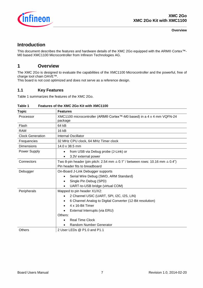
This document describes the features and hardware details of the XMC 2Go equipped with the ARM® Cortex™-M0 based XMC1100 Microcontroller from Infineon Technologies AG.
1 Overview
The XMC 2Go is designed to evaluate the capabilities of the XMC1100 Microcontroller and the powerful, free of charge tool chain DAVE™. This board is not cost optimized and does not serve as a reference design.
1.1 Key Features
Table 1 summarizes the features of the XMC 2Go.
Table 1 Features of the XMC 2Go Kit with XMC1100
Topic Features
Processor XMC1100 microcontroller (ARM® Cortex™-M0 based) in a 4 x 4 mm VQFN-24 package
Flash 64 kB
RAM 16 kB
Clock Generation Internal Oscillator
Frequencies 32 MHz CPU clock, 64 MHz Timer clock
Dimensions 14.0 x 38.5 mm
Power Supply from USB via Debug probe (J-Link) or
3.3V external power
Connectors Two 8-pin header (pin pitch: 2.54 mm ≙ 0.1” / between rows: 10.16 mm ≙ 0.4”)
Pin header fits to breadboard
Debugger On-Board J-Link Debugger supports
Serial Wire Debug (SWD, ARM Standard)
Single Pin Debug (SPD)
UART-to-USB bridge (virtual COM)
Peripherals Mapped to pin header X1/X2:
2 Channel USIC (UART, SPI, I2C, I2S, LIN)
6 Channel Analog to Digital Converter (12-Bit resolution)
4 x 16-Bit Timer
External Interrupts (via ERU)
Others:
Real Time Clock
Random Number Generator
Others 2 User LEDs @ P1.0 and P1.1
XMC 2Go XMC 2Go Kit with XMC1100 Overview
Board Users Manual 8 Revision 1.0, 2014-02-20
1.2 Block Diagram
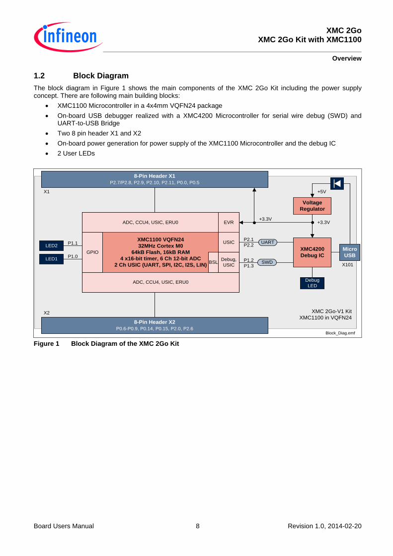
The block diagram in Figure 1 shows the main components of the XMC 2Go Kit including the power supply concept. There are following main building blocks:
XMC1100 Microcontroller in a 4x4mm VQFN24 package
On-board USB debugger realized with a XMC4200 Microcontroller for serial wire debug (SWD) and UART-to-USB Bridge
Two 8 pin header X1 and X2
On-board power generation for power supply of the XMC1100 Microcontroller and the debug IC
2 User LEDs
Figure 1 Block Diagram of the XMC 2Go Kit
XMC1100 VQFN24
32MHz Cortex M0
64kB Flash, 16kB RAM
4 x16-bit timer, 6 Ch 12-bit ADC
2 Ch USIC (UART, SPI, I2C, I2S, LIN)
USIC
EVR
LED2
ADC, CCU4, USIC, ERU0
ADC, CCU4, USIC, ERU0
XMC4200
Debug IC
Micro
USB
Voltage
Regulator
+5V
+3.3V
BSL
8-Pin Header X1
P2.7/P2.8, P2.9, P2.10, P2.11, P0.0, P0.5
8-Pin Header X2
P0.6-P0.9, P0.14, P0.15, P2.0, P2.6
XMC 2Go-V1 Kit
XMC1100 in VQFN24
LED1
Debug
LED
Block_Diag.emf
SWD
UART
Debug,
USIC
P1.1
P1.0GPIO
P2.1
P2.2
P1.2
P1.3
+3.3V
X1
X101
X2
XMC 2Go XMC 2Go Kit with XMC1100 Hardware Description
Board Users Manual 9 Revision 1.0, 2014-02-20
2 Hardware Description
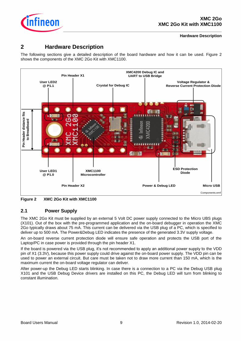
The following sections give a detailed description of the board hardware and how it can be used. Figure 2 shows the components of the XMC 2Go Kit with XMC1100.
Figure 2 XMC 2Go Kit with XMC1100
2.1 Power Supply
The XMC 2Go Kit must be supplied by an external 5 Volt DC power supply connected to the Micro UBS plugs (X101). Out of the box with the pre-programmed application and the on-board debugger in operation the XMC 2Go typically draws about 75 mA. This current can be delivered via the USB plug of a PC, which is specified to deliver up to 500 mA. The Power&Debug LED indicates the presence of the generated 3.3V supply voltage.
An on-board reverse current protection diode will ensure safe operation and protects the USB port of the Laptop/PC in case power is provided through the pin header X1.
If the board is powered via the USB plug, it’s not recommended to apply an additional power supply to the VDD pin of X1 (3.3V), because this power supply could drive against the on-board power supply. The VDD pin can be used to power an external circuit. But care must be taken not to draw more current than 150 mA, which is the maximum current the on-board voltage regulator can deliver.
After power-up the Debug LED starts blinking. In case there is a connection to a PC via the Debug USB plug X101 and the USB Debug Device drivers are installed on this PC, the Debug LED will turn from blinking to constant illumination.
Voltage Regulator &
Reverse Current Protection Diode
Micro USB
XMC1100
Microcontroller
User LED1
@ P1.0
User LED2
@ P1.1
Pin Header X2
Pin Header X1
Power & Debug LED
Pin
He
ad
er
dis
tan
ce
fit
s
to B
rea
db
oa
rd
ESD Protection
Diode
Crystal for Debug IC
XMC4200 Debug IC and
UART to USB Bridge
Components.emf

XMC 2Go XMC 2Go Kit with XMC1100 Hardware Description
Board Users Manual 10 Revision 1.0, 2014-02-20
2.2 Pin Header Connector
The pin headers X1 and X2 can be used to extend the evaluation board or to perform measurements on the XMC1100. The order of pins available at X1 and X2 corresponds to the pinning schema of the XMC1100 Microcontroller in the TSSOP-16 pin package. The pinning table is also printed onto the bottom side of the PCB.
Figure 3 Pinning of Pin Header
2.3 User LEDs
The port pins P1.0 and P1.2 of the XMC1100 on the XMC 2Go Kit are connected to LEDs exclusively.
Table 2 Pins used for the User LEDs
LED Port Pin
LED1 P1.1
LED2 P1.0
P0.6
Pin_Header.emf
P0.7
P0.8
P0.9
P0.14
P0.15
P2.0
P2.6
P0.
5P0.
03.
3VGND
P2.
11
P2.
10
P2.
9P2.
7
X1
X2

XMC 2Go XMC 2Go Kit with XMC1100 Production Data
Board Users Manual 11 Revision 1.0, 2014-02-20
2.4 Debugging and UART Communication
The on-board debugger supports 2-pin Serial Wire Debug (SWD), Single Pin Debug (SPD) and UART communication. Both require the installation of Segger’s J-Link Driver which is part of the DAVE™ installation. DAVE™ is a high-productivity development platform for the XMC microcontroller families to simplify and shorten SW development. It can be downloaded at www.infineon.com/dave. The latest Segger J-Link Driver can be downloaded at http://www.segger.com/jlink-software.html.
During installation of the J-Link driver you will be asked for the installation of optional components. For support of the UART communication take care to install the CDC USB driver (Composite Device Class). Therefore select the option “Install USB Driver for J-Link-OB with CDC” as shown in Figure 4.
Figure 4 Recommended Installation Options for the J-Link driver
The XMC1100 on the XMC 2Go Kit is configured to SWD1 mode. Use the “BMI Get Set” tool integrated into DAVE™ to configure the XMC1100 to e.g. SPD1 mode if required. Take care: Unintended use of the “BMI Get Set” tool can cause the XMC 2Go Kit not to work anymore, e.g. when configuring the XMC1100 to SWD0, SPD0 mode or to productive user mode.
Note: Do not configure the XMC1100 on the XMC 2Go Kit to SWD0, SPD0 or to productive user mode.
Table 3 shows the pin assignment of the XMC1100-VQFN24 used for debugging and UART communication.
Table 3 XMC1100 Pins used for Debugging and UART Communication
Pin Function Input / Output Port Pin
Data pin for Debugging via SWD/SPD I/O P1.3
Clock pin for Debugging via SWD O P1.2
Transmit Pin for UART Communication O P2.1
Receive Pin for UART Communication I P2.2
3 Production Data
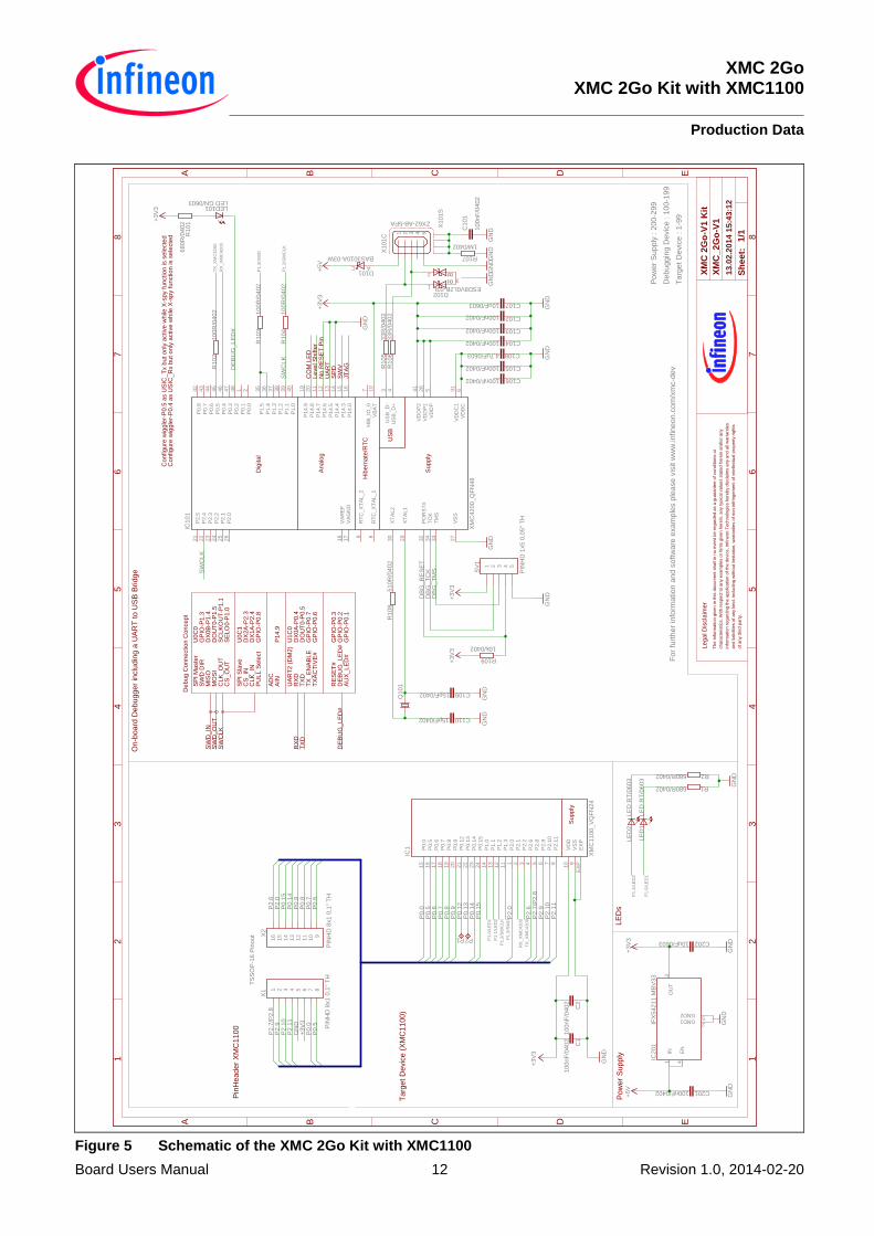
3.1 Schematics
The schematic of the XMC 2Go Kit can be found in Figure 5.
XMC 2Go XMC 2Go Kit with XMC1100 Production Data
Board Users Manual 12 Revision 1.0, 2014-02-20
Figure 5 Schematic of the XMC 2Go Kit with XMC1100
Pow
er
Supply
: 2
00-2
99
Debuggin
g D
evic
e : 1
00-1
99
Targ
et D
evic
e : 1
-99
For
furt
her
info
rmation a
nd s
oftw
are
exam
ple
s p
lease v
isit w
ww
.infineon.c
om
/xm
c-d
ev
1 2 3 4 5 6 7 89
10
11
12
13
14
15
16
TS
SO
P-1
6 P
inout
+3V
3
+3V
3
+3V
3
+3V
3
+3V
3+
3V
3
100nF
/0402
100nF
/0402
100nF
/0402
100nF/0402
100nF/0402
100nF/0402
100nF/0402
100nF/0402
10uF/0603
4,7uF/0603
15pF/0402
15pF/0402
100nF/0402
10uF/0603
BAS3010A-03W
ESD8V0L2B-03L
GN
D
GN
D
GN
DG
ND
GN
D
GN
D
GN
D
GN
DG
ND
GN
DG
ND
GN
DG
ND
GN
DG
ND
GN
D
XM
C1100_V
QF
N24
XM
C4200_Q
FN
48
IFX
54211 M
BV
33
LE
D R
T/0
603
LE
D R
T/0
603
LED GN/0603
+5V
+5V
680R/0402
680R/0402
680R
/0402
100R
/0402 100R
/0402
100R
/0402
33R
/0402
33R
/0402
1M/0402
510R
/0402
10k/0402
PIN
HD
1x5 0
,05"
TH
PIN
HD
8x1 0
,1"
TH
PIN
HD
8x1 0
,1"
TH
ZX62-AB-5PA
+3V
3
DB
G_R
ES
ET
DB
G_T
CK
DB
G_T
MS
DE
BU
G_LE
D#
GN
D
P0.0
P0.0
P0.5
P0.5P
0.6
P0.6P
0.7
P0.7P
0.8
P0.8P
0.9
P0.9
P0.1
2P
0.1
3
P0.1
4
P0.1
4
P0.1
5
P0.1
5
P1.0
/LE
D1
P1.0
/LE
D1
P1.1
/LE
D2
P1.1
/LE
D2
P1.2
/SW
CLK
P1.2
/SW
CLK
P1.3
/SW
D
P1.3
/SW
D
P2.0
P2.0P
2.6
P2.6
P2.7
/P2.8
P2.7
/P2.8
P2.9
P2.9
P2.1
0
P2.1
0
P2.1
1
P2.1
1
RX
_X
MC
4200
RX
_X
MC
4200
SW
CLK
SW
CLK
TX
_X
MC
4200
TX
_X
MC
4200
C1
C2
C101
C102
C103
C104
C105
C106
C107
C108
C109
C110
C201
C202
ACD101
1
23
D102
EX
PE
XP
P0
.01
5
P0
.51
6
P0
.61
7
P0
.71
8
P0
.81
9
P0
.92
0
P0
.12
21
P0
.13
22
P0
.14
23
P0
.15
24
P1
.01
4
P1
.11
3
P1
.21
2
P1
.31
1
P2
.01
P2
.12
P2
.23
P2
.64
P2
.85
P2
.96
P2
.10
7
P2
.11
8
VD
D1
0
VS
S9
IC1
HIB
_IO
_0
7
P0
.02
P0
.11
P0
.24
8P
0.3
47
P0
.44
6P
0.5
45
P0
.64
4P
0.7
43
P0
.84
2
P1
.04
0P
1.1
39
P1
.23
8P
1.3
37
P1
.43
6P
1.5
35
P2
.02
6P
2.1
25
P2
.22
4P
2.3
23
P2
.42
2P
2.5
21
P1
4.0
16
P1
4.3
15
P1
4.4
14
P1
4.5
13
P1
4.6
12
P1
4.7
11
P1
4.8
20
P1
4.9
19
PO
RS
T#
32
RT
C_
XT
AL
_1
8
RT
C_
XT
AL
_2
9
TC
K3
4
TM
S3
3
US
B_
D+
4U
SB
_D
-3
VA
GN
D1
7V
AR
EF
18
VB
AT
10
VD
DC
6V
DD
C1
31
VD
DP
5V
DD
P1
28
VD
DP
24
1
VS
S2
7
XT
AL
12
9
XT
AL
23
0
IC101
EN
4
GND12
GND25
IN1
OU
T3
IC201
LE
D1
LE
D2
LED101
P1 P2
Q101
R1
R2
R101
R102
R103
R104
R105
R106
R107
R108
R109
1 2 3 4 5
SV
1
X1
X2
1 2 3 4 5
X101C
X101S
D1
D2
Supply
US
B
Supply
Analo
g
Dig
ital
Hib
ern
ate
/RT
C
A B C D E
12
34
56
78
A B C D E
12
34
56
78
XM
C_
2G
o-V
1
13.0
2.2
014 1
5:4
3:1
2
1/1
Sh
ee
t:
Legal D
iscla
imer
The info
rmation g
iven in this
docum
ent shall
in n
o e
vent be r
egard
ed a
s a
guara
nte
e o
f conditio
ns o
r
chara
cte
ristics. W
ith r
espect to
any e
xam
ple
s o
r hin
ts g
iven h
ere
in, any typic
al valu
es s
tate
d h
ere
in a
nd/o
r any
info
rmation r
egard
ing the a
pplic
ation o
f th
e d
evic
e, In
fineon T
echnolo
gie
s h
ere
by d
iscla
ims a
ny a
nd a
ll w
arr
anties
and lia
bili
ties o
f any k
ind, in
clu
din
g w
ithout lim
itation, w
arr
anties o
f non-infr
ingem
ent of in
telle
ctu
al pro
pert
y r
ights
of any third p
art
y.
XM
C 2
Go
-V1
Kit
On-b
oard
Debugger
inclu
din
g a
UA
RT
to U
SB
Bridge
Configure
wig
gle
r-P
0.5
as U
SIC
_T
x b
ut only
active w
hile
X-s
py function is s
ele
cte
dC
onfigure
wig
gle
r-P
0.4
as U
SIC
_R
x b
ut only
active w
hile
X-s
py function is s
ele
cte
d
SC
LK
OU
T-P
1.1
DX
0B
-P1.4
SP
I S
lave
SW
D_O
UT
SW
CLK
MO
SI
CLK
_O
UT
MIS
O
CS
_IN
CLK
_IN
CS
_O
UT
SP
I M
aste
rU
0C
0
U0C
1
DO
UT
0-P
1.5
SE
LO
0-P
1.0
DX
2A
-P2.3
DX
1A
-P2.4
RX
DT
XD
UA
RT
2 (
DM
2)
RX
DT
XD
DX
0A
-P0.4
DO
UT
0-P
0.5
U1C
0
TX
AC
TIV
E#
GP
IO-P
0.6
RE
SE
T#
GP
IO-P
0.3
DE
BU
G_LE
D#
DE
BU
G_LE
D#
GP
IO-P
0.2
TX
_E
NA
BLE
GP
IO-P
0.7
SW
D D
IRG
PIO
-P1.3
SW
D_IN
AD
CA
INP
14.9
PU
LL S
ele
ct
GP
IO-P
0.8
AU
X_LE
D#
GP
IO-P
0.1
UA
RT
SP
D
No R
ES
ET
Pin
Level S
hifte
rC
OM
LE
D
SW
VJT
AG
Pow
er
Supply
Debug C
onnection C
oncept
LE
Ds
Pin
Header
XM
C1100
Targ
et D
evic
e (
XM
C1100)
XMC 2Go Kit XMC1100 in VQFN24
XMC 2Go XMC 2Go Kit with XMC1100 Production Data
Board Users Manual 13 Revision 1.0, 2014-02-20
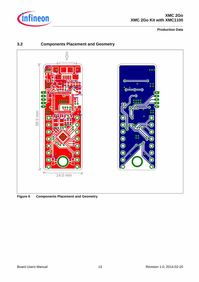
3.2 Components Placement and Geometry
Figure 6 Components Placement and Geometry
14.0 mm
38.5
mm
C1C2
C101
C102
C103
C104
C105
C106
C107
C108C109
C110
C201C202
D101
D102
IC1
IC101
IC201
LED1LED2
LED101
P1
P2
Q101
R1R2
R101
R102
R103
R104
R105R106
R107
R108
R109
X101
XMC 2Go XMC 2Go Kit with XMC1100 Production Data
Board Users Manual 14 Revision 1.0, 2014-02-20
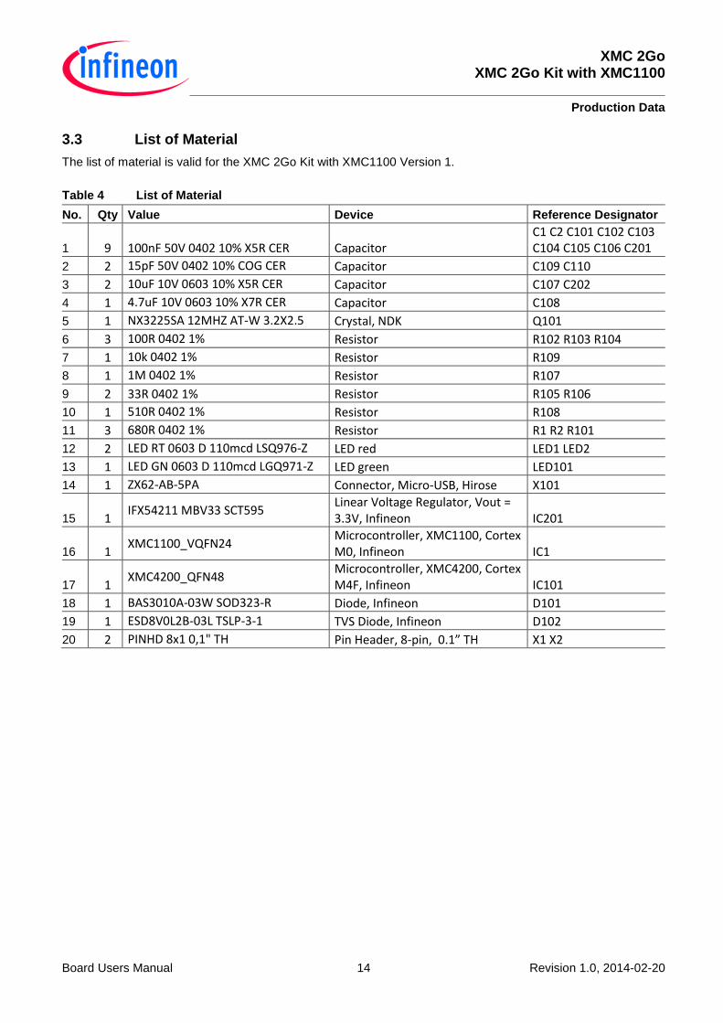
3.3 List of Material
The list of material is valid for the XMC 2Go Kit with XMC1100 Version 1.
Table 4 List of Material
No. Qty Value Device Reference Designator
1 9 100nF 50V 0402 10% X5R CER Capacitor C1 C2 C101 C102 C103 C104 C105 C106 C201
2 2 15pF 50V 0402 10% COG CER Capacitor C109 C110
3 2 10uF 10V 0603 10% X5R CER Capacitor C107 C202
4 1 4.7uF 10V 0603 10% X7R CER Capacitor C108
5 1 NX3225SA 12MHZ AT-W 3.2X2.5 Crystal, NDK Q101
6 3 100R 0402 1% Resistor R102 R103 R104
7 1 10k 0402 1% Resistor R109
8 1 1M 0402 1% Resistor R107
9 2 33R 0402 1% Resistor R105 R106
10 1 510R 0402 1% Resistor R108
11 3 680R 0402 1% Resistor R1 R2 R101
12 2 LED RT 0603 D 110mcd LSQ976-Z LED red LED1 LED2
13 1 LED GN 0603 D 110mcd LGQ971-Z LED green LED101
14 1 ZX62-AB-5PA Connector, Micro-USB, Hirose X101
15 1 IFX54211 MBV33 SCT595
Linear Voltage Regulator, Vout = 3.3V, Infineon IC201
16 1 XMC1100_VQFN24
Microcontroller, XMC1100, Cortex M0, Infineon IC1
17 1 XMC4200_QFN48
Microcontroller, XMC4200, Cortex M4F, Infineon IC101
18 1 BAS3010A-03W SOD323-R Diode, Infineon D101
19 1 ESD8V0L2B-03L TSLP-3-1 TVS Diode, Infineon D102
20 2 PINHD 8x1 0,1" TH Pin Header, 8-pin, 0.1” TH X1 X2

w w w . i n f i n e o n . c o m
Published by Infineon Technologies AG