evaluation of cots sige, soi, & mixed signal electronic ... electronic parts for extreme...
TRANSCRIPT

Evaluation of COTS SiGe, SOI, & Mixed Signal Electronic Parts for Extreme Temperature Use in NASA Missions
Richard L. PattersonNASA Glenn Research Center
Ahmad HammoudASRC Aerospace Corporation
1
National Aeronautics and Space Administration
NEPP Electronic Technology WorkshopJune 22-24, 2010

To be presented at the 1st NASA Electronic Parts and Packaging (NEPP) Program Electronic Technology Workshop June 22-24, 2010, NASA GSFC, Greenbelt, MD. 2
Introduction
• Brief description of NEPP Task # 10-281 (Continuing)“Reliability of SiGe, SOI, and Advanced Mixed Signal Devices for Cryogenic Space Missions”
• Goal, approach, schedule, and status of Task
• Technical highlights
• Plans

To be presented at the 1st NASA Electronic Parts and Packaging (NEPP) Program Electronic Technology Workshop June 22-24, 2010, NASA GSFC, Greenbelt, MD. 3
NEPP Task # 10-281 (Continuing)Reliability of SiGe, SOI, and Advanced Mixed Signal
Devices for Cryogenic Space MissionsDescription:
FY10 Plans:
Schedule: Deliverables:
Space exploration missions require electronics that operate under extreme temperatures. SiGe devices utilize band gap engineering in their design to enable low temperature operation, and SOI parts offer good radiation tolerance and high temperature operation capability. This task focuses on establishing reliability of SiGe, SOI, and advanced mixed signal devices for use in extreme temperature space exploration missions. COTS parts and flight-like hardware will also be evaluated by determining their performance under extreme temperatures and thermal cycling. The generated data will establish safe operating areas and identify degradation modes, and the information will be disseminated to mission planners and system designers to establish risk factors associated with the use of such parts at extreme temperature in space applications.
Identify and acquire COTS parts and flight-like hardware.
Determine part/circuit operational requirements.
Conduct screening tests at extreme temperatures.
Perform combined thermal/electrical tests.
Determine the effects of wide temperature thermal cycling.
Publish reports and disseminate information.
Issue technical reports documenting reliability of selected SiGe, SOI, and advanced mixed signal devices for extreme temperature operation.
Publish results on NEPP website and at professional conferences and disseminate information to mission planners and system designers.
Submit quarterly progress reports.
O N D J F M A M J J A SAcquire COTS & mission-related devicesScreen devices at extreme temperaturesDown-select promising devicesPerform thorough characterizationPerform thermal cycling on selected partsAnalyze & document resultsPublish BOK reports & disseminate info. ♦ ♦ ♦ ♦Propose 2011 follow-on task ♦
2009 2010

To be presented at the 1st NASA Electronic Parts and Packaging (NEPP) Program Electronic Technology Workshop June 22-24, 2010, NASA GSFC, Greenbelt, MD. 4
Goals
• Establish a technology base for the development of electronic systems, using COTS parts, capable of extreme temperature operation for space exploration missions
• Disseminate information and transfer technology to NASA mission groups and aerospace designers

To be presented at the 1st NASA Electronic Parts and Packaging (NEPP) Program Electronic Technology Workshop June 22-24, 2010, NASA GSFC, Greenbelt, MD. 5
Expected Impact to Community
Traditional approach to extreme temp operation
• Passive or active thermal control• Warm electronic box• Radioisotope heater units
Impact of “extreme temperature electronics”
• Simplify thermal management• Improve energy density and system efficiency• Improve reliability• Reduce overall system mass• Reduce development and launch costs

To be presented at the 1st NASA Electronic Parts and Packaging (NEPP) Program Electronic Technology Workshop June 22-24, 2010, NASA GSFC, Greenbelt, MD. 6
Status/Schedule
O N D J F M A M J J A SAcquire COTS & mission-related devicesScreen devices at extreme temperaturesDown-select promising devicesPerform thorough characterizationPerform thermal cycling on selected partsAnalyze & document resultsPublish tech reports & disseminate info. ♦ ♦ ♦ ♦Propose 2011 follow-on task ♦
2009 2010

To be presented at the 1st NASA Electronic Parts and Packaging (NEPP) Program Electronic Technology Workshop June 22-24, 2010, NASA GSFC, Greenbelt, MD. 7
FY10 Highlights/Accomplishments• Submitted deliverable test report “Evaluation of a
High Temperature SOI Half-Bridge MOSFET Driver, Type CHT-HYPERION”
• Submitted deliverable test report “Use of a Frequency Divider to Evaluate an SOI NAND Gate Device, Type CHT-7400, for Wide Temperature Applications”
• Submitted deliverable test report “Evaluation of a Programmable Voltage-Controlled MEMS Oscillator, Type SiT3701, over a Wide Temperature Range”

To be presented at the 1st NASA Electronic Parts and Packaging (NEPP) Program Electronic Technology Workshop June 22-24, 2010, NASA GSFC, Greenbelt, MD. 8
Target Temperature (°C)
Venus +480Lunar Surface -230 → +120
Mars Surface -125 → +20
Jupiter -160 → +300
Europa (Jupiter) -160 → -120
Titan (Saturn) -180 → -150
NASA Applications

To be presented at the 1st NASA Electronic Parts and Packaging (NEPP) Program Electronic Technology Workshop June 22-24, 2010, NASA GSFC, Greenbelt, MD. 9
Silicon Germanium (SiGe)Utilize band-gap engineering to tailor properties such as preventing carrier freeze-out
e.g. Diodes, HBT’s, Op Amps, VCO’s
Silicon-on-Insulator (SOI)Offer reduced leakage current, high temperature capability, improved radiation tolerance, & less power consumption
e.g. Timers, Op Amps, Logic, MOSFET’s, Drivers, VREF
Advanced Mixed SignalEmploy new material & design technologies to enhance performance and improve reliability
e.g. MEMS Oscillators, VCO’s, Converters, VREG

To be presented at the 1st NASA Electronic Parts and Packaging (NEPP) Program Electronic Technology Workshop June 22-24, 2010, NASA GSFC, Greenbelt, MD. 10
Forward V-I characteristics of a SiGe diode, type SG 21-41
0 0.4 0.8 1.2Forward Voltage (V)
0
1
2
3
4
Forw
ard
Cur
rent
(A)
20 °C-50 °C
-100 °C-150 °C
-195 °C
+85 °C
SiGe diode operated successfully to -195 °C with increase in forward voltage drop.

To be presented at the 1st NASA Electronic Parts and Packaging (NEPP) Program Electronic Technology Workshop June 22-24, 2010, NASA GSFC, Greenbelt, MD. 11
0 0.4 0.8 1.2 1.6Forward Voltage (V)
0
1
2
3
4
Forw
ard
Cur
rent
(A)
20 °C
-195 °C+85 °C
0 0.4 0.8 1.2 1.6Forward Voltage (V)
0
1
2
3
4
Forw
ard
Cur
rent
(A)
20 °C
-195 °C
+85 °C
Pre-cycling Post-cycling
SiGe power diode, type SGD-P51 (12 cycles; -195 °C to +85 °C)
Thermal cycling had little effect on operation of SiGe diode.

To be presented at the 1st NASA Electronic Parts and Packaging (NEPP) Program Electronic Technology Workshop June 22-24, 2010, NASA GSFC, Greenbelt, MD. 12
IC versus VCE of a SiGe HBT, type L2-32, at +20 °C
0 4 8 12VCE (V)
0
0.2
0.4
0.6
0.8
I C (A
) Ib= 10 mA
8
6
4
2
Room temperature baseline info on a SiGe HBT.

To be presented at the 1st NASA Electronic Parts and Packaging (NEPP) Program Electronic Technology Workshop June 22-24, 2010, NASA GSFC, Greenbelt, MD. 13
IC versus VCE of a SiGe HBT, type L2-32, at -195 °C
0 4 8 12VCE (V)
0
0.2
0.4
0.6
0.8
I C (A
)
Ib= 10 mA
8
6
4
2
Increased current gain at -195 °C for same SiGe HBT device.

To be presented at the 1st NASA Electronic Parts and Packaging (NEPP) Program Electronic Technology Workshop June 22-24, 2010, NASA GSFC, Greenbelt, MD. 14
IC versus VCE of a SiGe HBT, type L2-32, at +85 °C
0 4 8 12VCE (V)
0
0.2
0.4
0.6
0.8
I C (A
)
Ib= 10 mA
8
6
4
2
Slightly increased current gain at +85 °C compared to room temp gain.

To be presented at the 1st NASA Electronic Parts and Packaging (NEPP) Program Electronic Technology Workshop June 22-24, 2010, NASA GSFC, Greenbelt, MD. 15
Current gain of a SiGe HBT, type GPD 16-25, power transistor
-200 -160 -120 -80 -40 0 40 80 120Temperature (°C)
0
20
40
60
80
100
120
140
160
180
200
220
240
260
280
300
DC
Cur
rent
Gai
n (I C
/ IB)
SiGe HBTHBT-16-25 Pre Cycling
VCE = 8 VIB = 50 mA
Very large increase in DC current gain at low temperatures for SiGe HBT power transistor.

To be presented at the 1st NASA Electronic Parts and Packaging (NEPP) Program Electronic Technology Workshop June 22-24, 2010, NASA GSFC, Greenbelt, MD. 16
Output frequency of a SiGe VCO, type MAX2622
0 1 2 3 4Tune Voltage (V)
750
800
850
900
950
1000
Freq
uenc
y (M
Hz)
-50 °C
T = -195 °C-150 °C-100 °C
+20 °C
+85 °C
SiGe voltage controlled oscillator operating over wide temperature range.

To be presented at the 1st NASA Electronic Parts and Packaging (NEPP) Program Electronic Technology Workshop June 22-24, 2010, NASA GSFC, Greenbelt, MD. 17
Class V rad-tolerant THS4304-SP silicon germanium amplifier
Frequency (Hz)Frequency (Hz)108 109
Gai
n (d
B)
Gai
n (d
B)
-10-8-6
-4
-2024
68
1012
14
161820
Legend-195 °C-175 °C-150 °C25 °C150 °C175 °C200 °C
Wide temperature range operation of Class V Rad-Tolerant SiGe amplifier.

To be presented at the 1st NASA Electronic Parts and Packaging (NEPP) Program Electronic Technology Workshop June 22-24, 2010, NASA GSFC, Greenbelt, MD. 18
SOI operational amplifier , type HTOP-01
Frequency (kHz)1 10 100 1000 10000
Gai
n (d
B)
-30
-20
-10
0
10
Pre Cycling Data+200 ºC+100 ºC+22 ºC-100 ºC-190 ºC
Cryogenic operation of a 200 °C rated silicon-on-insulator op amp.

To be presented at the 1st NASA Electronic Parts and Packaging (NEPP) Program Electronic Technology Workshop June 22-24, 2010, NASA GSFC, Greenbelt, MD. 19
Gain of an SOI CHT-OPA operational amplifier
1 10 100 1000 10000Frequency (kHz)
-30
-20
-10
0
10
Gai
n (d
B)
= +200 °C. +100 °C, +25 °C& -100 °C/ -190 °C
1 10 100 1000 10000Frequency (kHz)
-30
-20
-10
0
10
Gai
n (d
B)
= +200 °C, +25 °C/ -190 °C
After thermal cycling.Before thermal cycling.
Thermal cycling had little effect on operation of SOI operational amplifier.
To be presented at the 1st NASA Electronic Parts and Packaging (NEPP) Program Electronic Technology Workshop June 22-24, 2010, NASA GSFC, Greenbelt, MD. 20
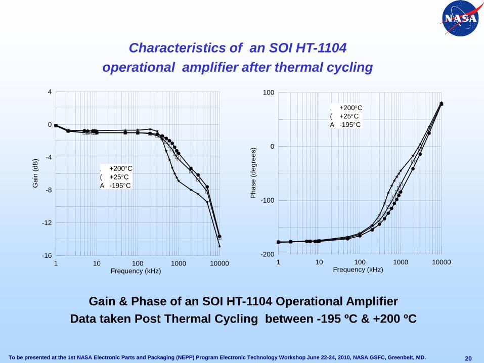
1 10 100 1000 10000Frequency (kHz)
-16
-12
-8
-4
0
4
Gai
n (d
B)
, +200°C( +25°CA -195°C
1 10 100 1000 10000Frequency (kHz)
-200
-100
0
100
Phas
e (d
egre
es)
, +200°C( +25°CA -195°C
Characteristics of an SOI HT-1104 operational amplifier after thermal cycling
Gain & Phase of an SOI HT-1104 Operational AmplifierData taken Post Thermal Cycling between -195 ºC & +200 ºC

To be presented at the 1st NASA Electronic Parts and Packaging (NEPP) Program Electronic Technology Workshop June 22-24, 2010, NASA GSFC, Greenbelt, MD. 21
Gain of a SiGe/SOI , type OPA-211,operational amplifier
1 10 100 1000 10000Frequency (kHz)
-16
-12
-8
-4
0
4
Gai
n (d
B) ! +140 °C
( +25 °C< -175 °C
Broad frequency range gain stability of a unique SiGe/SOI op amp over a wide temperature range.

To be presented at the 1st NASA Electronic Parts and Packaging (NEPP) Program Electronic Technology Workshop June 22-24, 2010, NASA GSFC, Greenbelt, MD. 22
Silicon-on-Insulator CHT-555 timer
Trigger (1), output (2), and threshold (3) signals of a high temperatureSOI CHT-555 timer at room temperature and at -195 °C.
20 °C -195 °C

To be presented at the 1st NASA Electronic Parts and Packaging (NEPP) Program Electronic Technology Workshop June 22-24, 2010, NASA GSFC, Greenbelt, MD. 23
Divide-by-2 circuit using SOI quad NAND devices
-192 °C +225 °C
Successful operation of SOI digital circuit over a very wide temperature range.

To be presented at the 1st NASA Electronic Parts and Packaging (NEPP) Program Electronic Technology Workshop June 22-24, 2010, NASA GSFC, Greenbelt, MD. 24
SOI CMOS voltage reference, type CHT-BG-050
-200 -150 -100 -50 0 50 100 150 200Temperature (°C)
4.9
5
5.1
5.2
5.3
Out
put V
olta
ge (V
)
. VIN= 9 Volts# VIN= 12 Volts+ VIN= 15 Volts! VIN= 18 Volts
0 1 2 3 4Output Current (mA)
4.9
5
5.1
5.2
5.3
Out
put V
olta
ge (V
)
, +20 °C* +100 °C
" -100 °C
/ -195 °C
Excellent stability of SOI CMOS voltage reference from -100 °C to +100 °C.

To be presented at the 1st NASA Electronic Parts and Packaging (NEPP) Program Electronic Technology Workshop June 22-24, 2010, NASA GSFC, Greenbelt, MD. 25
SOI full-bridge driver, type CHT-FBDR
+225°C
+25°C -190°C
No effect of temperature on operation of an SOI full-bridge driver.

To be presented at the 1st NASA Electronic Parts and Packaging (NEPP) Program Electronic Technology Workshop June 22-24, 2010, NASA GSFC, Greenbelt, MD. 26
Temperature ( °C)-200 -100 0 100 200
RD
S (o
n), D
rain
-Sou
rce
Res
ista
nce
(Ohm
)
0.0
0.5
1.0
1.5
2.0
Temperature ( °C)-200 -100 0 100 200
VG
S(th
), G
ate
Thre
shol
d V
olta
ge (V
)
0
1
2
3
4
5
Characteristics of an N-channel SOI MOSFET, type NMOS80
RDS held steady between -195 °C and -20 °C but increased with further increasein temperature. VGTH exhibited linear decrease with increase in temperature.

To be presented at the 1st NASA Electronic Parts and Packaging (NEPP) Program Electronic Technology Workshop June 22-24, 2010, NASA GSFC, Greenbelt, MD. 27
All-silicon oscillator, type ASFLM-1
-80 -40 0 40 80 120 160Temperature (°C)
92
96
100
104
108
90
94
98
102
106
110
Freq
uenc
y (k
Hz)
-80 -40 0 40 80 120 160Temperature (°C)
48
49
50
51
52
48.5
49.5
50.5
51.5
Dut
y C
ycle
(%)
Good frequency stability from +120 °C to -25 °C.

To be presented at the 1st NASA Electronic Parts and Packaging (NEPP) Program Electronic Technology Workshop June 22-24, 2010, NASA GSFC, Greenbelt, MD. 28
Temperature (°C)-150 -100 -50 0 50 100 150
Freq
uenc
y (M
Hz)
0.5
0.6
0.7
0.8
0.9
1.0
1.1
1.2
1.3
1.4
1.5
Temperature (°C)-150 -100 -50 0 50 100 150
Dut
y C
ycle
(%)
0
20
40
60
80
100
MEMS silicon oscillator, type EMK21
Excellent frequency stability from +110 °C to -110 °C.

To be presented at the 1st NASA Electronic Parts and Packaging (NEPP) Program Electronic Technology Workshop June 22-24, 2010, NASA GSFC, Greenbelt, MD. 29
Floating-gate voltage reference, type X60008B
-200 -150 -100 -50 0 50Temperature (°C)
2.492
2.494
2.496
2.498
2.5
2.502
2.504
Out
put V
olta
ge (V
)
, VIN = 4.5 Volts* VIN = 5.0 Volts/ VIN = 6.0 Volts" VIN = 6.5 Volts
0 2 4 6 8 10Output Current (mA)
2.48
2.485
2.49
2.495
2.5
2.505
Out
put V
olta
ge (V
)
, Temp = 20 °C* Temp = -100 °C/ Temp = -195 °C
Excellent voltage stability from +25 °C to -195 °C.

To be presented at the 1st NASA Electronic Parts and Packaging (NEPP) Program Electronic Technology Workshop June 22-24, 2010, NASA GSFC, Greenbelt, MD. 30
MEMS voltage-controlled oscillator, type SiT3701
Temperature (°C)-200 -150 -100 -50 0 50 100
Freq
uenc
y (k
Hz)
79960
80000
80040
80080
80120
80160Vin =
0.75 V
1.25 V
1.75 V
0 V
1.5 V
0.5 V
1.0 V
0.25 V
Input Voltage, Vin (V)0.00 0.25 0.50 0.75 1.00 1.25 1.50 1.75
Freq
uenc
y (k
Hz)
79995
79996
79997
79998
79999
80000
80001
80002
80003
Temperature
-100 °C+85 °C+22 °C0 °C-50 °C
This oscillator showed excellent frequency stability between +85 °C and -100 °C.

To be presented at the 1st NASA Electronic Parts and Packaging (NEPP) Program Electronic Technology Workshop June 22-24, 2010, NASA GSFC, Greenbelt, MD. 31
Passives: wire-wound resistor (93J10K) & NP0 capacitor (SM041A164K)
TemperatureTemperature-200 -150 -100 -50 0 50 100 150 200
Res
ista
nce
(kΩ
)R
esis
tanc
e (kΩ
)
0
5
10
15
20
TemperatureTemperature-200 -150 -100 -50 0 50 100 150 200
Cap
acita
nce
(uF)
Cap
acita
nce
(uF)
0.00
0.05
0.10
0.15
0.20
Dis
sipa
tion
Fact
orD
issi
patio
n Fa
ctor
0.000
0.002
0.004
0.006
0.008
0.010
Capacitance
Dissipation Factor
These are special passive devices that have good stability over a wide temperature range.

To be presented at the 1st NASA Electronic Parts and Packaging (NEPP) Program Electronic Technology Workshop June 22-24, 2010, NASA GSFC, Greenbelt, MD. 32
New high temperature (150 ºC) operational amplifier, type LM2904WH
Frequency (kHz)1 10 100 1000 10000
Gai
n (
dB
)
-30
-25
-20
-15
-10
-5
0
5
Legend
+ 190 ºC+ 150 ºC+ 22 ºC- 100 ºC- 150 ºC
This is a new silicon operational amplifier for high temperature use. Rated at +150 °C, it also operated down to -150 °C.

To be presented at the 1st NASA Electronic Parts and Packaging (NEPP) Program Electronic Technology Workshop June 22-24, 2010, NASA GSFC, Greenbelt, MD. 33
3.3V, 10W rad-hard DC/DC converter
-200 -180 -160 -140 -120 -100 -80 -60 -40 -20 0 20 40
Temperature (°C)
0.8
0.9
1.0
1.1
Nor
mal
ized
Out
put V
olta
ge
-200 -180 -160 -140 -120 -100 -80 -60 -40 -20 0 20 40
Temperature (°C)
0.0
0.2
0.4
0.6
0.8
1.0
1.2
Nor
mal
ized
Effi
cien
cy
IOUT
0.5A
1.0A
1.5A2.0A2.5A
This rad-hard DC/DC converter operated well down to -140 °C.

To be presented at the 1st NASA Electronic Parts and Packaging (NEPP) Program Electronic Technology Workshop June 22-24, 2010, NASA GSFC, Greenbelt, MD. 34
Test facilities at NASA Glenn Research Center
There is a 240 liter liquid nitrogen dewar on the right, and there are two environmental chambers in the background.

To be presented at the 1st NASA Electronic Parts and Packaging (NEPP) Program Electronic Technology Workshop June 22-24, 2010, NASA GSFC, Greenbelt, MD. 35
Test facilities at NASA Glenn Research Center
This equipment was used to evaluate semiconductor devices at extremely low temperatures and at radio frequencies.

To be presented at the 1st NASA Electronic Parts and Packaging (NEPP) Program Electronic Technology Workshop June 22-24, 2010, NASA GSFC, Greenbelt, MD. 36
Test facilities at NASA Glenn Research Center
This chamber was used to evaluate a radio frequency amplifier for low temperature operation in a new space shuttle landing system.

To be presented at the 1st NASA Electronic Parts and Packaging (NEPP) Program Electronic Technology Workshop June 22-24, 2010, NASA GSFC, Greenbelt, MD. 37
Plans for FY11
Identify and acquire SiGe, SOI, and advanced mixed signal electronic parts with potential for use in extreme temperature space missions. (Q1-Q2 FY11)
Setup test facilities, determine part operational requirements, and establish test matrix. (Q1-Q2 FY11)
Perform testing on acquired SiGe, SOI, advanced mixed signal parts, and flight-like hardware over an extended temperature range. (Q1-Q4 FY11)
Determine performance of promising parts under wide temperature thermal cycling. (Q3-Q4 FY11)
Document data and disseminate information to the NASA designers and mission planners. (Q4 FY11)
Publish results on NASA NEPP Website, in technical journals, and at engineering conferences. (Q4 FY11)