evolving solid state storage - storage networking industry · pdf fileflash cache. ssd array +...
TRANSCRIPT
Evolving Solid State Storage
Bob Beauchamp – EMC Distinguished Engineer
Macro trends Scale-out and multi-core processors Flash hitting its stride …but at a cliff? Looming DRAM challenge The rise of low-latency DMA networks
Infiniband PCIe
Should storage just look like memory?

feeding the new server
more cores = more parallelism = more simultaneous I/O requests
more physical memory = more VMs, larger active datasets
more data, accessed more rapidly = more throughput
Process
Architecure
Nehalem
Haswell
Sandy Bridge
“flash makes things faster”
good idea #1: use flash to replace HDD well defined interface, functional envelope pre-existing HW ecosystem unmodified SW stack
100x performance gains measured relative to disk Reliability and sufficient endurance now proven
after some notable failures… …a number of “good-enough” FTLs emerge and evolve

“flash makes things faster”
good idea #2: put flash as close to processing as possible Use as Direct Attach Storage (DAS) when application can achieve sufficient functionality, reliability and availability Use as cache when need to preserve external array functionality, reliability, and availability
SW stacks change: Avoid HDD-centric “optimizations” Begin to exploit features of FTL
Simplicity of variable size writes: compression No torn writes at power fail (write atomicity) “Almost for free” copy on write

Oracle OLTP Workload Performance
9,834 24,700
82,483 89,546 109,271
251,565
-
50,000
100,000
150,000
200,000
250,000
300,000
Baseline (all SASdrives)
Baseline +server flash
cache
All flash array Baseline + arrayflash cache
Baseline + arrayand server flash
caches
Server flash
DB transactions per minute

Oracle OLTP Workload Performance
transaction response time
20
7
2 2 1
0 -
5
10
15
20
25
Baseline (all SASdrives)
Baseline + serverflash cache
SSD array + serverflash cache
Baseline + arrayflash cache
Baseline + array andserver flash cache
Server flash
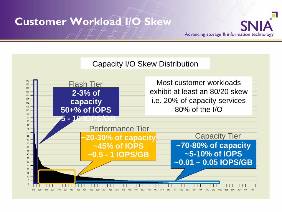
Customer Workload I/O Skew
Capacity I/O Skew Distribution
Most customer workloads exhibit at least an 80/20 skew i.e. 20% of capacity services
80% of the I/O
2-3% of capacity
50+% of IOPS ~5 - 10 IOPS/GB
Flash Tier
~20-30% of capacity ~45% of IOPS
~0.5 - 1 IOPS/GB
Performance Tier
~70-80% of capacity ~5-10% of IOPS
~0.01 – 0.05 IOPS/GB
Capacity Tier

CAGR
58%
50%
enterprise flash deployment landscape
2011 2012 2013 2014 2015
Storage
Mainstream server
$3.1B
$.5B
flash in today’s datacenter
$1B of investment is fueling two contrasting deployment models
venture investments in flash related technologies
$22 $10
$86
$142 $174
$281 $320
• flash controllers • SSDs, EFDs • PCIe cards • all flash arrays
• PCIe cards, initially as DAS
• arrays : ease of adoption • many credible suppliers today
•performance intensive (latency, throughput)
•casual or no protection
•hybrid arrays •better, faster, cheaper •internal tiering
•all-flash-arrays
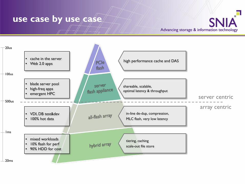
use case by use case
20us
500us
1ms
20ms
shareable, scalable, optimal latency & throughput
tiering, caching scale-out file store
high performance cache and DAS
100us
in-line de-dup, compression, MLC flash, very low latency
• cache in the server • Web 2.0 apps
• blade server pool • high-freq apps • emergent HPC
• VDI, DB test&dev • 100% hot data
• mixed workloads • 10% flash for perf • 90% HDD for cost
server centric
array centric

The State of Solid State
Healthy competition across price, capacity, performance Viable second-sources slow proprietary alternatives Proven reliability and endurance
Standards gaining momentum NVMe & SCSIe promotes common HW/SW interface, standard drivers, and device interoperability hot swappable 2.5” SFF SAS/SATA/PCIe
“you cannot NOT afford flash” Choose: lower cost same performance, or pay for performance
We are past the first knee of the adoption S-curve

Flash’s Future
Will Ming the Merciless’ laws of physics stop him?

NAND FABs 1. Samsung 2. Toshiba/Sandisk 3. Micron/Intel 4. Hynix
• 21EB in 2012 (vs. 440EB of HDD)
• 100EB by 2014
Moore’s law doubles NAND capacity every 18
months
NAND FABs produce 14M wafers annually, grows to 20M
by 2014
14.2%
the macro view of NAND flash

Gordon Moore was right…
…at least for a while 2 years since IM and Toshiba announced 19-20nm Toshiba publicly stated 1y (2D) this year; 50nm 3D NAND 2015
??
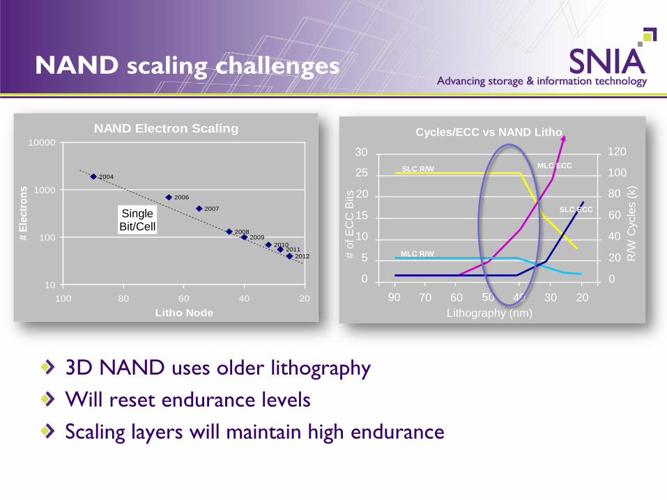
NAND scaling challenges
3D NAND uses older lithography Will reset endurance levels Scaling layers will maintain high endurance
SLC R/W
NAND Electron Scaling
20122011
20102009
2008
2007
2006
2004
10
100
1000
10000
20406080100
Litho Node
# El
ectro
ns
SingleBit/Cell
0
5
10
15
20
25
30
0
20
40
60
80
100
120
90 70 60 50 40 30 20Lithography (nm)
# of
EC
C B
its
R/W
Cyc
les
(k)
Cycles/ECC vs NAND Litho
SLC R/W
MLC R/W
SLC ECC
MLC ECC
0
5
10
15
20
25
30
0
20
40
60
80
100
120
90 70 60 50 40 30 20Lithography (nm)
# of
EC
C B
its
R/W
Cyc
les
(k)
Cycles/ECC vs NAND Litho
SLC R/W
MLC R/W
SLC ECC
MLC ECC

Fab scaling challenges
Older lithography of 3D NAND makes fabs more affordable
3D NAND success ensures flash as the storage juggernaut through the end of this decade

Getting storage closer to the processor
Direct Mapped Access Storage Class Memory
The Big Memory Era

Persistent Memory (PM) Defined
A non-volatile storage device Performance approaching that of DRAM
Can be accessed like memory via loads/stores
Comparable or better cost than DRAM Next generation NVM will eventually have better density, price, and power per bit than DRAM
Likely to occur within 3-5 years Multiple contenders: ST-MRAM, ReRAM, PCM, …
Current NAND flash already has much better density, price and power characteristics
Challenges are latency and maybe endurance

SCM Approaching DRAM Speeds
But how long can an application and/or processor wait on memory? When should the application treat the access like storage and yield the processor?
?? Application Stalled
Application Pended
Application Load or Store
PM
1,000,000 Potential stalled instructions 10 100 1,000 10,000 100,000
PCIe Flash
Ctxt Sw Cost
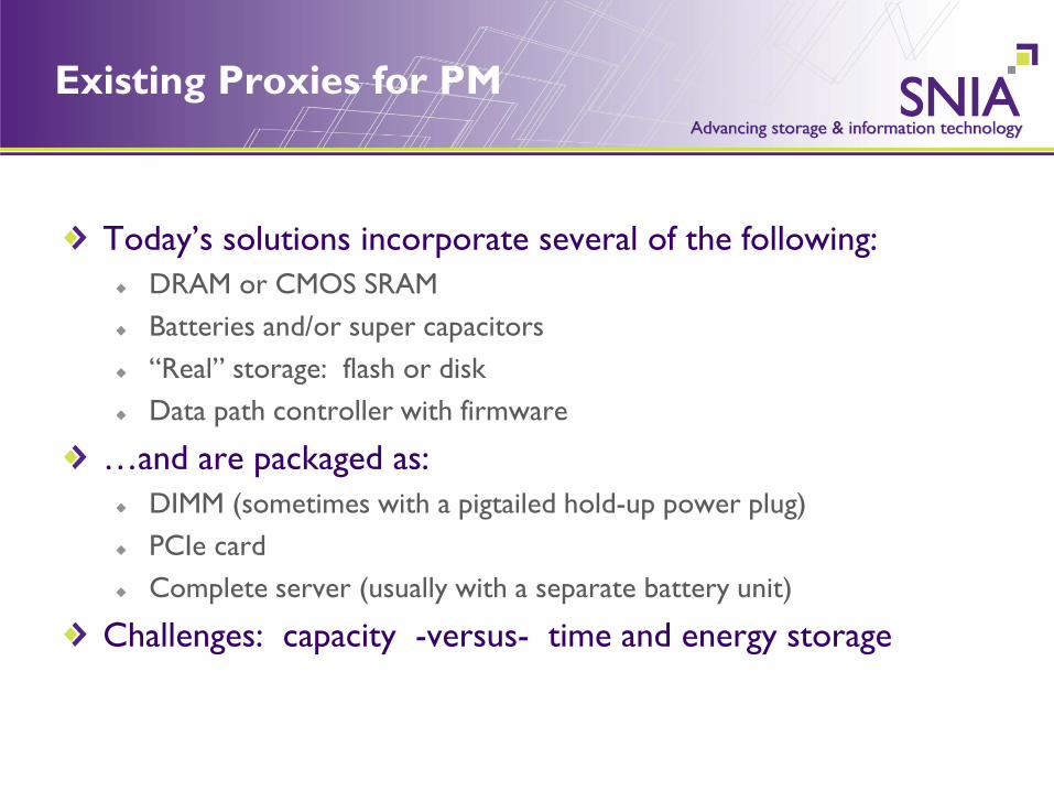
Existing Proxies for PM
Today’s solutions incorporate several of the following: DRAM or CMOS SRAM Batteries and/or super capacitors “Real” storage: flash or disk Data path controller with firmware
…and are packaged as: DIMM (sometimes with a pigtailed hold-up power plug) PCIe card Complete server (usually with a separate battery unit)
Challenges: capacity -versus- time and energy storage

Today’s memory model
Dynamically allocated (ie, anonymous) memory Application grow and shrink virtual memory as needed – ex. malloc() / free() Data then accessed via loads and stores Anonymous memory is typically backed and bounded by the size of swap
Memory mapped files Application maps some or all of one or more files into its virtual address space - ex. open() / mmap() Data then accessed via loads and stores
Explicit-IO memory Application explicitly accesses portions of one or more files through buffers in its virtual address space – ex. open() / read() / write() Objects in buffers then accessed via loads and stores
Virtual address space
Dynamically allocated memory
(malloc)
Explicit-IO memory
(read/write)
DRAM 10’s GB
Files, Partitions, Raw Disks
Swap
Memory-mapped files (mmap)
Operating system treats DRAM as a cache and manages data placement in physical memory
– Swap, pager, fileIO

Does existing model just work?
On the whole, yes. …but the devil is always in the (corner case) details
Seems equivalent to buffered explicit IO Many corners compared to unbuffered explicit IO
Is scope /granularity of flush semantics sufficient ? Sufficient visibility to know all memory queues are flushed ? Want HW flush that has no invalidate side-effect
Still need power hold up to flush buffers Can this be kept to one or two digits of microseconds ? Standardize flushing as HW / FW function ?

Any other impediments ?
Mapped-File not as popular as Explicit-IO. Why ? Education ? Inertia ? (if its not broke, don’t fix it) Data structure complexity ? Lack of eco system ? Doesn’t perform as well ? Reliability complexity ?
Does it matter? Can’t a library layer provide the Explicit-IO interface ?

Exciting Times
NVM is an exciting direction for storage and computing Many opportunities lie ahead We need your help and input on this NVM journey Thank You