executive summary - sheffield · executive summary introduction ... feature is functional and...
TRANSCRIPT

I
EXECUTIVE SUMMARY
INTRODUCTION/BACKGROUND
The Smart Home has the rapid development with computer technology and electronic
information technology. Especially in recent years, it is more and more attention in
impetus of the Internet of Things. The main subject completed a smart home system
hardware design and software design, and with the peripheral modules to form a
complete smart home system.
AIMS AND OBJECTIVES
The project is designed to implement a simple smart home system that can be applied
in an ordinary family. It has the following principles in the design: simple, practical,
inexpensive, stable and durable, scalability, energy saving. While the project in
development and design process can enhance their embedded product development
capabilities, as well as in practice identify problems, problem-solving abilities.
ACHIEVEMENTS
Complete such a low smart home system, it has low price and practical functionality,
so that ordinary consumers can enjoy the experience fun brings intelligence, but also
to guide them to the demand for smart home, the smart home industry will promote
development.
CONCLUSIONS / RECOMMENDATIONS
The realization of this project has a smart home’s basic functions. The system is not
the pursuit of sophisticated features and gorgeous appearance, mainly focused on
practical convenience, low prices and other characteristics of the low-end market to
fill the vacancy of smart home products.

II
ABSTRACT
In analyzing the issue of the smart home research status, trend, research significance,
the proposed smart home system based on embedded system design, and its main
feature is functional and practical, simple, inexpensive and easy to install.
Hardware aspects are using STM32F103RBT6 as the system master chip, with
Ethernet chips, sensors and other devices for PCB design. Schematic diagram of each
module was designed using Altium Designer, and then import the schematic to the
PCB files, it need the rational distribution of components on the PCB, rational layout.
Lastly, complete PCB design. After the completion of the system board components
of the welding for power debug, modify some unreasonable circuits, achieve emulator
download and serial ISP download.
Software aspects are using ST's official firmware library, and RealView MDK to
design base drivers, Serial and Ethernet drivers; while using Easy Programming
Language to write the upper application software, and achieve home appliances,
curtains, lightings’ local or remote control and other smart home basic functions.

III
ACKNOWLEDGEMENTS
First of all, I would like to thank my supervisor Dr Jun Liu. He provided me a good
study guide, and often teaches me how to do things, this gives me a lot of harvest. The
first time to design hardware devices, it improve the personal ability, and to lay the
foundation for future work.
I thank my family and friends for their support. Especially my parents, they are my
strongest backing, and gave me a strong spiritual power.
TABLE OF CONTENTS
Chapter 1 - Introduction ............................................................................................. 2
1.1. Background and Motivation .......................................................................... 2
1.1.1. The Internet of Things and the Smart Home ......................................... 2
1.1.2. The development of Smart Home .......................................................... 3
1.2. Problem Definition......................................................................................... 3
1.3. Aims and Objectives ...................................................................................... 4
1.3.1. Aims ....................................................................................................... 4
1.3.2. Objectives .............................................................................................. 5
1.4. Project Management ...................................................................................... 5
1.4.1. Requirements of the design .................................................................... 5
1.4.2. Schedule ................................................................................................. 7
Chapter 2 - Literature Review/Research ................................................................... 8
2.1. The selection of chips .................................................................................... 8
2.1.1. Microcontroller unit ............................................................................... 8
2.1.2. Ethernet control unit ............................................................................ 11
2.2. The principles of circuit schematic design................................................... 12
2.2.1. Infrared transceiver .............................................................................. 12
2.2.2. Relay .................................................................................................... 14
2.2.3. Magnetron ............................................................................................ 15
2.2.4. Temperature sensor .............................................................................. 16
2.2.5. Photoresistor ........................................................................................ 17
2.2.6. Comparator .......................................................................................... 18
2.3. Development environment and design applications .................................... 19
2.3.1. Altium Designer ................................................................................... 19
2.3.2. RealView MDK(Keil μVision) ............................................................ 20
2.3.3. EPL (Easy Programming Language) ................................................... 21
Chapter 3 - Hardware Design ................................................................................... 23
3.1. Core Module ................................................................................................ 23

1
3.2. Ethernet module ........................................................................................... 27
3.3. Magnetic induction module ......................................................................... 28
3.4. Infrared part module .................................................................................... 30
3.5. Temperature module .................................................................................... 31
3.6. Light intensity module ................................................................................. 32
3.7. Relay Module ............................................................................................... 33
Chapter 4 - Software Design ..................................................................................... 35
4.1. Base Driver .................................................................................................. 35
4.1.1. Magnetic induction module and Light intensity module ..................... 35
4.1.2. Relay Module ....................................................................................... 37
4.1.3. Temperature module (Appendix) ......................................................... 37
4.1.4. Infrared part module (Appendix) ......................................................... 38
4.2. The application of the smart home system .................................................. 39
Chapter 5 - Results..................................................................................................... 46
5.1. PCB Design .................................................................................................. 46
5.2. Weld and debug ........................................................................................... 48
5.3. Software ....................................................................................................... 50
5.3.1. Base Driver .......................................................................................... 50
5.3.2. The application..................................................................................... 51
Chapter 6 - Conclusions and Recommendations .................................................... 54
REFERENCES ........................................................................................................... 56
Appendices .................................................................................................................. 58

2
Chapter 1 - Introduction
1.1. Background and Motivation
1.1.1. The Internet of Things and the Smart Home
Currently, the Internet of Things become a hot area of global concern, following the
Internet are considered to be the most significant future technological innovation, it
are also an important component of the new generation of information technology.
The Internet of Things that are material objects connected to the Internet. This has
two meanings: First, The Internet of Things are still the core and foundation of the
Internet, the Internet is based on the extension and expansion of the network; Second,
the extension and expansion of its clients to any goods between the information
exchange and communication.
the Internet of Things are the use of a variety of information technology and
information transmission and processing technology, the state of the managed objects
can be perceived, also can be identified, and the formation of the topical application
of network not only provides the sensor networking connection, which itself also has
intelligent processing capability to implement intelligent control of the object. In the
near future, it is to bring these topical application of networks through the Internet and
communication network connected together to form the objects and things linked to a
huge network.
The smart home is an embodiment under the influence of the Internet of Things, it
belongs to an important branch of the Internet of Things. The development of smart
home is diversified technology, it is also very rich. Overall, the development of smart
home has gone through four generations. The Smart Home is a house as a platform, it
is the integration of automation and control systems, computer network systems and
network communication technology in one of the network of intelligent home control
systems, use of relevant technology to home life related facilities integration, build
efficient residential facilities affairs and family schedule management system.

3
A smart home system through the home networking technology to connect together
with a variety of devices, providing lighting control, home appliance control, burglar
alarm, environmental monitoring, infrared repeater, curtain control, heating control,
indoor and outdoor remote control, mobile remote control, and programmable timing
control and other functions and means. Compared with ordinary home, the smart
home features are not only traditional residence features both information appliances,
equipment automation, network communication, collection systems, structures,
services and management as one of the living environment, it are providing a full
range of information exchange capabilities to help people effectively arrange time,
optimizing the way of people’s life, to help families communication with external,
improve home safety, convenience, comfort, artistry, and to achieve eco-friendly
living environment.
1.1.2. The development of Smart Home
Since the last century by Microsoft's "Venus" program, it is causing the smart home
concept and market impulses, the smart home system has sprung up, highlighting the
vitality and dynamism of its development. But after 20 years’ development, the smart
home market is not imagination and so hot. In fact, the development and
popularization of smart home has a very good technical base, market infrastructure
and demand basis. But the products, systems and market demand that exists among
the great contradictions. It cannot lead to the rapid development of smart home.
The smart home control system’s market is not an ordinary commodity trading, but
rather a systematic project, which involves a lot of technique that involves every
aspect of people's life, the smart home control system's ultimate goal is an ideal, it is a
concept, and in order to have a good development, guided by long-term development
of mind, the spirit of simplification, practical, cost-effective, fit -market philosophy,
religious studies people's life, habits, spiritual and cultural needs and see it the highest
goal, using various technical means to achieve it.
1.2. Problem Definition
Because people's expectations for the smart home are too large. With the media,
marketing overstated, the function and role of smart home are too myth. It seems to be

4
omnipotent, but some future technology, high-end technology in the civilian market is
not immediately popular. This allows people to the smart home have too high
functionality expectations, and the products currently on the market can offer far
failed to meet people's psychological expectations.
Smart home contains many functions, as technology advances and market demand ,it
will continue to expand its functionality increases. This makes the operation more
complex, simple things complicated. Intelligent complex operation does not bring joy
and convenience to people's life, on the contrary leads to trouble and use
psychological burden.
The smart home should be a fashion product, and is the modern scientific and
technological achievements of human civilization as a reward on people's life, but to
get real in everyday life popularity, its price must be always the same threshold, only
when its price dropped to the extent that people can receive only "blowout" type of
market demand. However, fashion and novelty are synonymous with high-end prices,
how to handle this relationship between the two is the key to market penetration.
Now the smart home does not get a good general, which has a main reason is no
uniform standards and protocols. The smart home is a multi- industry, cross-coverage
systems engineering, the equipment manufacturers follow different interface
standards and protocols production equipment, the result is interoperability between
different devices becomes very difficult. Therefore, the establishment of common
standards and protocols followed in the development of smart home must solve the
problem.
1.3. Aims and Objectives
1.3.1. Aims
This project investigates the embedded system in networked Smart Home systems,
and designs control procedures to achieve control in networked Smart Home systems.
The aim of this project is to build a better design about centralized control of
household appliances and other equipment.

5
1.3.2. Objectives
1) Research the background of the Internet of Things, and relative applications.
2) Understand the smart home system, and design requirements of a networked
control system, to achieve the distributive, dynamic and collaborative features of
household equipment. As well as some home appliances to achieve local, remote,
automatic, manual and timing intelligent control. In order to meet the practical
features, design standard interface device to combine existing equipment.
3) Study the related circuitry knowledge, design the exterior necessary electric
circuit to achieve the requirements of a networked smart home system.
4) Develop an embedded system hardware framework. And integrate the PCB of the
various subsystems and the embedded system, and form a complete networked
smart home system.
5) Use the C code program to design embedded system, implement the requirements
for the smart home. And use the Easy Programming Language to set up an
application to achieve the local and remote coordinated control with computers.
1.4. Project Management
1.4.1. Requirements of the design
Three sensor modules: an indoor light intensity and temperature sensor module,
an outdoor light intensity module, and finally a magnetic induction module, these
three modules are the signal back to the embedded system, the purpose is to show
the indoor temperature, through the embedded Sets the specified temperature
controlled heater power, and to determine the light intensity control electric
curtains and lights on and off.
Wired control module (To control the power of various devices)
Infrared remote appliance module, the purpose is to design a self- IR learning
module, press the send through an external infrared remote control signals, this
module to learn this signal buttons attached to their function, to combine a

6
number of existing infrared remote control lights and remote air conditioning and
other appliances control.
To design an embedded system, computer software interface to the user terminal
and manual and automatic timed intelligent control, the main control panel
interface is designed individually for each module, and expanded to meet the
needs.
Each module combines the real-life use of rational design needs to consider, such as
220V control relay type appliance needs rationality, the external power supply
designed for stability and so on.
Finally, since the actual test requires that the above relates to an external device,
unified with LED lights to indicate the work of these various modules, each large
independent power supply module, wired control design standard interface between
modules via cable connection.

7
1.4.2. Schedule

8
Chapter 2 - Literature Review/Research
2.1. The selection of chips
2.1.1. Microcontroller unit
Cortex-M3 is the first 32-bit standard processor based on ARMv7-M architecture,
with low power consumption, short interrupt latency, low commissioning costs and
many other advantages. It is designed for micro-control system, the steam system in
the body. Industrial control systems and wireless networks, power consumption and
cost-sensitive embedded applications to achieve high performance. It greatly
simplifies the programming complexity, combines high performance, low power, low
cost in totally.
Cortex-M3 processor is including the processor cores, Nested Vectored Interrupt
Controller, Memory Protection Unit, the bus interface unit and trace debug unit and so
on in the structure.
STM32 family of processors is currently divided into three series, STM32F101 is a
standard type series, working at 36MHZ; STM32F103 is enhanced series, working at
72MHz, with more on-chip RAM and richer peripherals; STM32F105 and
STM32F107 is the latest generation of connectivity products, increasing the full-
speed USB interface and hardware support IEEE1558 precision Time Protocol
Ethernet interface. Standard STM32 processor series is an entry product, its price is
only equivalent to 16-bit MCU, but it has a 32-bit MCU performance. Its peripheral
configuration will provide excellent connectivity and control. Enhanced product will
be 32-bit MCU performance and efficiency leads to a new level. The series of Cortex-
M3 core operating at 72MHz. End of the operation can be realized. And its peripheral
configuration can bring excellent connectivity and control.
In terms of using the same platform for the development of multiple projects, STM32
is a very good choice. Because in all STM32 family of products, both for only a small
amount of storage space needed to ask and pins, but also to meet the need for more

9
storage space and a fine pin; Existing suitable for high-performance applications, but
also to meet the low power requirements; both for low-cost simple applications, but
also to meet the high-end complex applications.
This selection of core chip is STM32F103RBT6, it belongs to the STM32 family of
enhanced high specification chips. In the specific configuration of different types of
chips are also different.
Inside the processor of STM32F103RBT6 has a rich peripheral interface, so that it can
be widely used in industrial control, building security, information appliances, digital
products and so on.

10
Using LQFP64 package structure, with up to 128Kbytes of Flash and 20Kbytes of
SRAM, support clock, reset, power management, and a large number of peripherals,
the debug mode supports serial wire debug (SWD) and JTAG interfaces also support
Cortex- M3 embedded tracking module.
Figure 2-1 Physical Structure
Figure 2-2 Pin map

11
2.1.2. Ethernet control unit
The rapid development of Internet, the network users are increased by times. In the
use of general purpose processor (GPU) to access to the Internet at the same time,
various household appliances, PDA, instrumentation, industrial production data
acquisition and control equipment are gradually towards network, to share vast
resources in Internet. The Ethernet after 20 years of development has become an
indispensable part of the underlying link in Internet. Embedded equipment price,
volume and real-time characteristics, in some applications, especially network
development on a standard processor incomparable advantages. In the process of
network development, the first problem to be solved is connected with Ethernet
network, i.e., how will the general-purpose processor network connection device
(Ethernet controller) applied to the development of Embedded Network
ENC28J60 is an industry standard serial peripheral interface (SPI) independent
Ethernet controller. It can be used as Ethernet interface controller of any SPI equipped.
ENC28J60 compliance with all IEEE802.3 specification, using a series of packet
filtering mechanism to the incoming packet is limited. It also provides an internal
DMA module, to realize fast data throughput and hardware support for the IP
checksum calculation. Communication with the main controller through the
realization of the two interrupt pin and SPI, high data transmission rate up to 10Mb/s.
Two pins dedicated connection for the LED, the network activity status indication. A
simplified block diagram of the ENC28J60 is shown in figure 1-1. Figure 1-2 shows
the typical application circuit of the device. The single chip is connected to the rate of
10Mbps Ethernet, only ENC28J60, two pulse transformer and some passive
components can be.
Figure 2-3 External connection

12
Table 2-1 Parameter information
Parameter Name Value
MAC Yes
PHY Yes
Standalone Ethernet Controller 10Base-T
TX/RX RAM Buffer(bytes) 8192
Max. Speed (MHz) 25
Op. Voltage (V) 3.3
Interface SPI
Temp. Range Min. (°C) -40
Temp. Range Max. (°C) 85
Interrupt Pin 1
LEDs 2
2.2. The principles of circuit schematic design
2.2.1. Infrared transceiver
Infrared remote control technology has been widely used in home appliances and
industrial control system. In this system, to realize the control function of home
appliances through the infrared remote control function, need to design infrared
transceiver, and master the principle of its operation.
Red light wavelength is 0.62 μ m~0.76 μ m, longer than the wavelength of light called
infrared light. Infrared remote control is the use of near infrared between 0.76 μ
m~1.5 μ m transmits the control signal. The infrared characteristic does not interfere
with other electrical appliances, it will not affect the surrounding environment. Circuit
debugging simple, if the transmitted signal coding, can realize the multi-channel
infrared remote control function.
Infrared remote control system in general by the infrared transmitting device and an
infrared receiving device is composed of two parts. The infrared transmitting device is

13
composed of the infrared coding chip, power supply and an infrared transmitting
circuit; the infrared receiving device consists of an infrared receiving circuit, infrared
decoder chip, power supply. Usually in order to make the signal can be transferred,
the sending end baseband binary signal modulated pulse train signal, transmitted
through the infrared emission tube. The commonly used way is through the pulse
width to achieve the signal modulation ((PWM) and the interval between bursts to
realize the signal of the pulse duration modulation (PPM) two methods. This system
adopts PWM mode, through the realization of the timer PWM output STM32. Figure
2-4 is the basic structure of infrared remote control system.
Figure 2-4 Transceiver principle diagram
Infrared wavelength infrared light emitting diode was about 0.94 μ m, appearance and
common led the same, but different colours, usually transparent color. The infrared
receiving tube is a photosensitive diode, used for infrared receiving diode under
reverse bias, it can work with high sensitivity. Because the transmitting power of the
infrared light emitting diodes are small, weak signal received by the infrared receiving
tube, so the receiver to increase high gain amplifier circuit. Figure 2-5 is a pin out
infrared transceiver, two on the right are two kinds of infrared receiving tube.
Figure 2-5 Pin map

14
Many kinds of infrared receiving head, pin definition is not the same, there are usually
three pin, which comprises a power supply pin, ground and signal output pin.
According to the receiver transmitter modulates the carrier should be different with
the corresponding demodulation frequency.
The infrared receiving head inside the gain of the amplifier is very big, very easy to
cause interference, therefore must add filter capacitor in the power supply pin
received, in general more than 22uf. Some manufacturers suggest between power
supply pin and access to power a 330 ohm resistor, to further reduce the interference
of power supply.
The working frequency of infrared transmitting and receiving device is 38KHz.
Infrared transmission, through the software modulation, the use of STM32 timer
mode PWM, 38KHz output data; the infrared receiving, via the STM32 timer input
capture function, the infrared signal decoding.
2.2.2. Relay
Relay is an electronic control device, it has a control system (also known as the input
circuit) and the controlled system (also known as the output circuit), usually used in
automatic control circuit. It is actually a "switch" to control a larger current with less
current, plays the automatic adjustment, safety protection, the role of conversion
circuit in circuit.
Figure 2-6 Various relay

15
2.2.3. Magnetron
Magnetron is a kind of passive electronic contact switch element, has the advantages
of simple structure, small volume to control advantages, its shell is generally a sealed
glass tube, the tube is provided with a two iron elastic spring plate, and has recorded a
rhodium metal inert gas. Usually, the glass tube two made of special material is
separated reed. When the magnetic material near the glass tube, the magnetic field
effect, two reed pipe is magnetized and attracted to each other contact, spring will pull
together, so that the circuit nodes are connected. External force disappears, two reeds
separated due to their flexibility, the line is disconnected. Therefore, as a way to
control the use of magnetic field signal line switching device, Magnetron can be used
as a sensor, used for counting, limit and so on (in security system is mainly used for
making Menci, window magnetic), and has been widely used in all kinds of
communication equipment. In practical application, is usually permanent magnet for
control of the two metal sheets or not. It with Holzer element almost, but the
principles are different in nature, is a kind of switching element to control the use of
magnetic signal, no magnetic disconnection, can be used to detect circuit or
mechanical motion state.
Figure 2-7 Various magnetron
Magnetron has the advantages of compact structure, light weight, can be installed in
the extremely limited space, very suitable for the miniaturization of equipment.
Switch Magnetron is hermetically sealed in an inert gas atmosphere, never in contact
with the external environment, long working life. Magnetron does not use the sliding
element, so it will not appear in all metal degradation of metal fatigue phenomenon, to
ensure the service life of the machine actually without limit.

16
2.2.4. Temperature sensor
DS18B20 is a kind of improved intelligent temperature sensor after DS1820 launched
the latest with DALLAS semiconductor company in the United States. Compared
with the traditional thermal resistance, it can directly read the measured temperature
and according to the actual requirements through simple programming 9 ~ 12 bit
digital readout mode. It can complete 9 bit and 12 bit digital value at 93.75 MS and
750 ms, and from DS18B20 to read out the information or write to DS18B20
information, I only need one line (line interface) to read and write, temperature
transform power from the data bus, the bus itself can also be articulated by the
DS18B20 to the power supply, and no additional power supply. So the use of
DS18B20 can make the system structure more simple, more reliable. He in the
temperature measurement precision, the conversion time, the transmission distance is
DS1820, resolution is improved greatly, bring more convenient and more satisfactory
results to the user.
Figure 2-8 Pin map
Temperature measurement principle of DS18B20, low temperature coefficient of the
crystal oscillation frequency is affected slightly by temperature, pulse signal to
generate the fixed frequency to the subtract counter 1, high temperature coefficient

17
changes with temperature of the crystal oscillation frequency change, signal generated
as the subtraction counting 2 pulse input, it also implies a counter gate the count,
when the door opened, pulse clock DS18B20 is generated on the low temperature
coefficient oscillator were counted, and then complete the temperature measurement.
Open time counting gate is determined by high temperature coefficient of the
oscillator, before each measurement, the corresponding -55 ℃ base are respectively
inserted into the subtract counter 1 and the temperature register, subtract counter 1
and the temperature register is a corresponding numerical preset at -55 ℃ . The
subtract counter for subtraction count pulse signal of 1 low temperature coefficient
crystal produced, when the preset counter value of 1 reduced to 0 when the
temperature register value plus 1, preset counter 1 will be loaded into the counter 1,
start to count low temperature pulse signal generated by the coefficient of crystal, so
until the subtract counter cycle 2 count to 0, accumulative temperature register values,
the values of temperature in the register is the measured temperature. Fig. 2 the slope
accumulator for nonlinear compensation and correction in the process of temperature
measurement, the output is used to modify the subtract counter preset value, as long
as the counting door has not yet closed just repeat the process until the temperature
reaches, register values measured temperature value, this is the DS18B20 temperature
measuring principle.
2.2.5. Photoresistor
Photosensitive resistance is also called light pipe, materials used for CDs, plus
selenium sulfide, aluminium, lead and bismuth sulfide materials. With these materials
of light in a specific wavelength, the resistance decreases rapidly. This is because the
light generated carriers are involved in conducting, in the role of drift motion under
applied electric field, the positive electron to the power supply, to supply anode hole,
so that the photosensitive resistor values decreased rapidly.

18
Figure 2-9 Photoresistor
2.2.6. Comparator
LM393 is a high gain, broadband device, like most comparator, if the output to the
input of a parasitic capacitance and coupling, are easy to produce oscillations. This
phenomenon only occurs when the comparator changes state, gap output voltage
transition, power and the bypass filter cannot solve this problem, design standard PC
board is helpful to reduce the input - output parasitic capacitance coupling. To reduce
the input resistance to less than 10K will reduce the feedback signal, and the increase
of even small amount of positive feedback (hysteresis 1.0~10mV) can lead to rapid
transformation, which could not produce the oscillation caused by the parasitic
capacitance, unless using lag, or directly into the IC (integrated circuit) and on the pin
plus the resistance will cause the input - output in a short transition period oscillation,
if the input signal is a pulse waveform, and the rise and fall time is quite fast,
hysteresis will not need.
Figure 2-10 LM393

19
Figure 2-11 The internal structure
Figure 2-12 Pin map
2.3. Development environment and design applications
2.3.1. Altium Designer
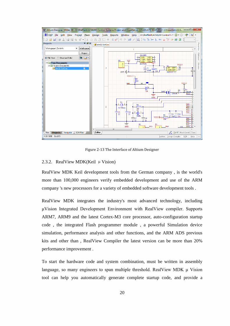
20
Figure 2-13 The Interface of Altium Designer
2.3.2. RealView MDK(Keil μVision)
RealView MDK Keil development tools from the German company , is the world's
more than 100,000 engineers verify embedded development and use of the ARM
company 's new processors for a variety of embedded software development tools .
RealView MDK integrates the industry's most advanced technology, including
μVision Integrated Development Environment with RealView compiler. Supports
ARM7, ARM9 and the latest Cortex-M3 core processor, auto-configuration startup
code , the integrated Flash programmer module , a powerful Simulation device
simulation, performance analysis and other functions, and the ARM ADS previous
kits and other than , RealView Compiler the latest version can be more than 20%
performance improvement .
To start the hardware code and system combination, must be written in assembly
language, so many engineers to span multiple threshold. RealView MDK μ Vision
tool can help you automatically generate complete startup code, and provide a

21
graphical window, as you easily modified. Whether a beginner or an experienced
engineer, can greatly save time, improve efficiency of development.
The device simulator RealView MDK can simulate the whole target hardware,
including fast instruction set simulation, the external signal and I/O simulation,
interrupt simulation, process all the peripheral equipment simulation. Development
Engineer in the absence of hardware conditions to start the software development and
debugging, the software and hardware development simultaneously, greatly shorten
the development cycle. But general ARM development tools only provide instruction
set simulator, can only support ARM kernel debugging.
The performance analyzer RealView MDK like Halley telescope, let you see farther
and more accurate, it helps you view code coverage, the running time of program,
function calls and other high-end control function, code optimization guide you
relaxed, become embedded development master. Usually these functions only
thousands of dollars worth of expensive Trace tools can provide.
Figure 2-14 The Interface of μVision
2.3.3. EPL (Easy Programming Language)

22
Figure 2-15 The Interface of EPL
23
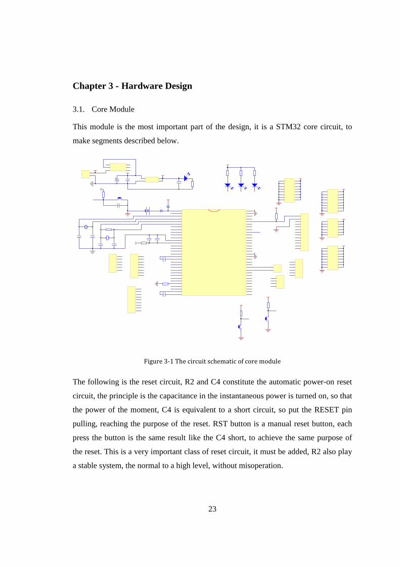
Chapter 3 - Hardware Design
3.1. Core Module
This module is the most important part of the design, it is a STM32 core circuit, to
make segments described below.
Figure 3-1 The circuit schematic of core module
The following is the reset circuit, R2 and C4 constitute the automatic power-on reset
circuit, the principle is the capacitance in the instantaneous power is turned on, so that
the power of the moment, C4 is equivalent to a short circuit, so put the RESET pin
pulling, reaching the purpose of the reset. RST button is a manual reset button, each
press the button is the same result like the C4 short, to achieve the same purpose of
the reset. This is a very important class of reset circuit, it must be added, R2 also play
a stable system, the normal to a high level, without misoperation.
V B A T
1
PC13/ANT1
2
PC14/OSC32
3
PC15/OSC32
4
PD0/OSCIN
5
PD1/OSCOUT
6
NRST
7
PC0/ADC10
8
PC1/ADC11
9
PC2/ADC12
1 0
PC3/ADC13
1 1
VSSA
1 2
V D D A
1 3
PA0/WKUP/ADC0/TIM2_CH1_ETR
1 4
PA1/ADC1/TIM2_CH2
1 5
PA2/U2_TX/ADC2/TIM2_CH3
1 6
PA3/U2_RX/ADC3/TIM2_CH4
1 7
VSS
1 8
V D D
1 9
PA4/SPI1_NSS/ADC4
2 0
PA5/SPI1_SCK/ADC5
2 1
PA6/SPI1_MISO/ADC6/TIM3_CH1
2 2
PA7/SPI1_MOSI/ADC7/TIM3_CH2
2 3
PC4/ADC14
2 4
PC5/ADC15
2 5
PB0/ADC8/TIM3_CH3
2 6
PB1/ADC9/TIM3_CH4
2 7
PB2/BOOT1
2 8
PB10/I2C2_SCL/U3_TX
2 9
PB11/I2C2_SDA/U3_RX
3 0
VSS
3 1
V D D
3 2
PB12/SPI2_NSS/I2C2_SMBAI/TIM1_BKIN
3 3
PB13/SPI2_SCK/TIM1_CH1N
3 4
PB14/SPI2_MISO/TIM1_CH2N
3 5
PB15/SPI2_MOSI/TIM1_CH3N
3 6
PC6
3 7
PC7
3 8
PC8
3 9
PC9
4 0
PA8/TIM1_CH1/MCO
4 1
PA9/U1_TX/TIM1_CH2
4 2
PA10/U1_RX/TIM1_CH3
4 3
PA11/CAN_RX/USBDM/TIM1_CH4
4 4
PA12/CAN_TX/USBDP/TIM1_ETR
4 5
PA13/JTMS/SWDIO
4 6
VSS
4 7
V D D
4 8
PA14/JTCK/SWCLK
4 9
PA15/JTDI
5 0
PC10
5 1
PC11
5 2
PC12
5 3
PD2/TIM3_ETR
5 4
PB3/JTDO/TRACESWO
5 5
PB4/JNTRST
5 6
PB5/I2C1_SMBAI
5 7
PB6/I2C1_SCL/TIM4_CH1
5 8
PB7/I2C1_SDA/TIM4_CH2
5 9
B O O T 0
6 0
PB8/TIM4_CH3
6 1
PB9/TIM4_CH4
6 2
VSS
6 3
V D D
6 4
U 2
STM32F103RBT6
1
2
H 1 V C C
G N D
I/O1
1
TAP1
2
I/O1
3
I/O2
4
TAP2
5
I/O2
6
ON/OFF1
B U T T O M
C 1
2 2 0 u F
C 2
1 0 4
V C C 5
G N D
1
O U T
2
I N
3
O U T
4
U 1
AMS1117-3.3
VCC3.3
R 1
1 k
DS1
L E D 1
B A T 1
C 4
1 0 4
D 1
1N4148
D 2
1N4148
r s t
R 2
1 0 k
VCC3.3
G N D
VCC3.3
reset
12
Y 2
8MHz
1 2
Y 1
32.768khz
R 4
1 M
C 5
2 2
G N D
reset
VCC3.3
R 5
1 0 K
G N D
G N D
R 3
1 K
VCC3.3
C 3
1 0 4
reset
VCC3.3
G N D
VCC3.3
G N D
PA0
PA1
PA2
PA3
PA4
PA5
PA6
PA7
PA8
PA9
PA10
PA11
PA12
PA13
PA14
PA15
PB0
PB1
PB2
PB3
PB4
PB5
PB6
PB7
PB8
PB9
PB10
PB11
PB12
PB13
PB14
PB15
PC0
PC1
PC2
PC3
PC4
PC5
PC6
PC7
PC8
PC9
PC10
PC11
PC12
PC13
PD2
1
2
T X
R X D
TXD
1
2
3
4
5
6
7
8
P 1
Header 8
PA0
PA1
PA2
PA3
PA4
PA5
PA6
PA7
1
2
3
4
5
6
P 2
Header 6
PC0
PC1
PC2
PC3
PC4
PC5
1
2
3
4
5
6
7
8
9
P 3
Header 9
PB1
PB0
PB2
PB11
PB10
PB12
PB13
PB14
PB15
1
2
3
4
P 4
Header 4
PC6
PC7
PC8
PC9
1
2
3
4
5
6
P 5
Header 6
PA8
PA9
PA10
PA11
PA12
PA13
1
2
3
4
5
6
7
8
9
1 0
1 1
1 2
1 3
Header 13
PA14
PA15
PC10
PC11
PC12
PD2
PB3
PB4
PB5
PB6
PB7
1 2
3 4
5 6
7 8
9 1 0
1 1 1 2
Header 6X2
VCC3.3
G N D
1 2
3 4
5 6
7 8
9 1 0
1 1 1 2
1 3 1 4
1 5 1 6
Header 8X2
V C C 5
G N D
1 2
3 4
5 6
7 8
9 1 0
1 1 1 2
1 3 1 4
1 5 1 6
Header 8X2
1 2
3 4
5 6
7 8
9 1 0
1 1 1 2
1 3 1 4
1 5 1 6
Header 8X2
VCC3.3
G N D
V C C 5
G N D
DS2
L E D 1
DS3
L E D 1
DS4
L E D 1
PA13PA14PA15
R 6
1 k
R 7
1 k
R 8
1 k
VCC3.3
K E Y 2
G N D
PA0
K E Y 3
G N D
PA1
R 9
1 k
R10
1 k
V C C 5
V C C 5
C 6
2 2
C 7
2 2
C 8
2 2
R 3
1 0 k
C 9
1 0 u f
C10
1 0 4
C11
1 0 4
VCC3.3
G N D
VCC3.3
G N D
C12
1 0 4

24
Figure 3-2 The circuit schematic of reset
The following is the heart of the circuit, which is the crystal oscillator circuit, the
system provides a stable clock, 8M is the core of the system, through the system
frequency after reaching 72M, 32.768K is a clock oscillator, providing time for the
system to use.
C5.C6 C7 C8 as the auxiliary vibrating capacitor, crystal can be equivalent to a
capacitor and a resistor in parallel and series two terminal network of a capacitor in
electric, electrical engineering on the network has two resonant frequencies, the
frequency divided the low frequency series resonant, high frequency parallel
resonance. Due to the characteristics of the crystal itself quite close to the two
frequency range, in this very narrow range of frequencies, crystal as an equivalent
inductance capacitance oscillator, so as long as the parallel at both ends of the
appropriate it will constitute a parallel resonant circuit. The parallel resonant circuit is
added to a negative feedback circuit can be a sine wave oscillation circuit, the crystal
is equivalent to the frequency range of inductance is very narrow, so even if the
parameter changes in other components of the great, the oscillator frequency will not
be much change. Crystal is an important parameter, which is the load capacitance
value, selection of shunt capacitor equal to the load capacitance value, you can get the
crystal resonant frequency nominal. Crystal oscillating circuit is generally in an
inverting amplifier (note is not connected to the two ends of the inverter amplifier)
C 4
1 0 4
r s t
R 2
1 0 k
VCC3.3
G N D
reset

25
crystal, and two capacitors are respectively connected at both ends of the crystal,
another end of each capacitor is connected to the ground, the two series capacitor
capacity value should be equal to the load capacitance, please pay attention to the
general IC pins have the equivalent input capacitance, this cannot be ignored. The
load capacitance general crystal is 15p or 12.5p, if we consider the equivalent input
capacitance component pin, two 22P capacitance oscillation circuit oscillator is a
good choice.
Figure 3-3
The following is a power supply circuit, BUTTON is a total system switch, The total
power to open or close, C1 and C2 is the power supply filter capacitor, play a
stabilizing role, C1 is capacitors, C2 is ceramic filter high frequency capacitance.
AMS1117 is the power conversion chip to convert 5V to 3.3V power supply into chip,
There are various of AMS1117, 2.5V 1.8V 3.3V, the use of 3.3V as system core
supply, DS1 is the power indicator, used to power supply indicator system, which
represents the electric light.
Figure 3-4
12
Y 2
8MHz
1 2
Y 1
32.768khz
R 4
1 M
C 5
2 2
G N D
P 2
C 6
2 2
C 7
2 2
C 8
2 2
1
2
H 1 V C C
G N D
I/O1
1
TAP1
2
I/O1
3
I/O2
4
TAP2
5
I/O2
6
ON/OFF1
B U T T O M
C 1
2 2 0 u F
C 2
1 0 4
V C C 5
G N D
1
O U T
2
I N
3
O U T
4
U 1
AMS1117-3.3
VCC3.3
R 1
1 k
DS1
L E D 1C 3
1 0 4

26
The overall core chip pin diagram, model is STM32F103RBT6, system memory is
128K, the system frequency is 72M, actual test results are quite satisfactory.
Figure 3-5 Pin map
Table 3-1 The list of components
Component Model
Interface H1.P1.P2.P3.P4.P5.P6.P7.P8.P9.TX1.
Resistance R1.R2.R3.R4.R5.R6.R7.R8.R9.R10.R11
Light-emitting diode DS1.DS2.DS3.DS4
Capacitance C1.C2.C3.C4.C5.C6.C7.C8.C9.C10.C11.C12
Battery BAT1
Button Rst1.KEY1.KE2
Crystal oscillator Y1.Y2
V B A T
1
PC13/ANT1
2
PC14/OSC32
3
PC15/OSC32
4
PD0/OSCIN
5
PD1/OSCOUT
6
NRST
7
PC0/ADC10
8
PC1/ADC11
9
PC2/ADC12
1 0
PC3/ADC13
1 1
VSSA
1 2
V D D A
1 3
PA0/WKUP/ADC0/TIM2_CH1_ETR
1 4
PA1/ADC1/TIM2_CH2
1 5
PA2/U2_TX/ADC2/TIM2_CH3
1 6
PA3/U2_RX/ADC3/TIM2_CH4
1 7
VSS
1 8
V D D
1 9
PA4/SPI1_NSS/ADC4
2 0
PA5/SPI1_SCK/ADC5
2 1
PA6/SPI1_MISO/ADC6/TIM3_CH1
2 2
PA7/SPI1_MOSI/ADC7/TIM3_CH2
2 3
PC4/ADC14
2 4
PC5/ADC15
2 5
PB0/ADC8/TIM3_CH3
2 6
PB1/ADC9/TIM3_CH4
2 7
PB2/BOOT1
2 8
PB10/I2C2_SCL/U3_TX
2 9
PB11/I2C2_SDA/U3_RX
3 0
VSS
3 1
V D D
3 2
PB12/SPI2_NSS/I2C2_SMBAI/TIM1_BKIN
3 3
PB13/SPI2_SCK/TIM1_CH1N
3 4
PB14/SPI2_MISO/TIM1_CH2N
3 5
PB15/SPI2_MOSI/TIM1_CH3N
3 6
PC6
3 7
PC7
3 8
PC8
3 9
PC9
4 0
PA8/TIM1_CH1/MCO
4 1
PA9/U1_TX/TIM1_CH2
4 2
PA10/U1_RX/TIM1_CH3
4 3
PA11/CAN_RX/USBDM/TIM1_CH4
4 4
PA12/CAN_TX/USBDP/TIM1_ETR
4 5
PA13/JTMS/SWDIO
4 6
VSS
4 7
V D D
4 8
PA14/JTCK/SWCLK
4 9
PA15/JTDI
5 0
PC10
5 1
PC11
5 2
PC12
5 3
PD2/TIM3_ETR
5 4
PB3/JTDO/TRACESWO
5 5
PB4/JNTRST
5 6
PB5/I2C1_SMBAI
5 7
PB6/I2C1_SCL/TIM4_CH1
5 8
PB7/I2C1_SDA/TIM4_CH2
5 9
B O O T 0
6 0
PB8/TIM4_CH3
6 1
PB9/TIM4_CH4
6 2
VSS
6 3
V D D
6 4
U 2
STM32F103RBT6

27
Diode D1.D2
Power chip U1 AMS1117
3.2. Ethernet module
The following is the network module circuit, the main chip is ENC28J60, this chip is
to resolve network connectivity problems, RJ45 is a standard network port, the rest
parts are ancillary components.
Figure 3-6
The following is the ENC28J60 system clock, the frequency is 25M, for the system to
provide a stable clock.
Figure 3-7
V C A P
1
VSS
2
C L K O U T
3
INT
4
NC/WDL
5
MISO
6
MOSI
7
SCK
8
C S
9
RST
1 0
VSSRX
1 1
TPIN-
1 2
TPIN+
1 3
RBIAS
1 4
V D D T X
1 5
TPOUT-
1 6
TPOUT+
1 7
VSSTX
1 8
V D D R X
1 9
VDDPLL
2 0
VSSPLL
2 1
VSSOSC
2 2
OSC1
2 3
OSC2
2 4
VDDOSC
2 5
L E D B
2 6
L E D A
2 7
V D D
2 8
U 2
ENC28J60
C 4 1 0 u f
G N D
NET_INT
NET_MISO
NET_MOSI
NET_S CK
NET_CS
NET_RST
TPIN-
TPIN+
R 7 2.3K
G N D
TPOUT-
TPOUT+
VCC33
G N D
L E D A
L E D B
Y 1 2 5 M
C11 2 2
C 9 2 2
G N D
VCC33
C 5
1 0 4
C 6
1 0 4
C 7
1 0 4
T D +
1
T D -
2
R D +
3
T C T
4
R C T
5
R D -
6
N C
7
CHS GND
8
LED(G)_A
9
LED(G)_K
1 0
LED(Y)_K
1 1
LED(Y)_A
1 2
SHILED
1 3
SHILED
1 4
J 1
RJ45
R 2 5 1 0
L E D A
L E D B
R 3 5 1 0
G N D
R 1 5 0
R 4 5 0
R 5 5 0
R 6 5 0
C10 1 0 3
C 8 1 0 3
L 1
1 0 0 u H
TPOUT+
TPOUT-
TPIN+
TPIN-
VCC33
VCC33
Y 1 2 5 M
C11 2 2
C 9 2 2

28
The following R1, R4, R5 and R6 are limiting resistor for the network interface, R2
and R3 are resistance to light, RJ45 network port is a standard 8-pin.
Figure 3-8
Table 3-2 The list of components
Component Model
Interface RJ45
Resistance R1.R2.R3.R4.R5.R6.R7
Light-emitting diode RJ45
Capacitance C4.C5.C6.C7.C8.C9.C10.C11
Network chip U2 ENC28J60
3.3. Magnetic induction module

29
Figure 3-9
R1 and D1 are the indicator circuit, to indicate whether the current signal, a signal
goes off without signal lights, U1 as the core device, Reed Switch, it also called
magnetron, the principle is there are two internal magnetic iron tablets, normality is
sucked side, when the external magnetic field, there is a large magnetic force will tend
to end, so did the switch, its interior is a vacuum with glass packaging.
U1 when subjected to a magnetic field, the lower end of the lower end of the lower,
R1, at the D1 end voltage of 0V so that LED will not light, 2 interface is parallel with
U1 upper, so also will be lower, then the signal is transmitted to the embedded system.
Table 3-3 The list of components
Component Model
Interface J1 HDR1X3
Resistance R1.10K
Light-emitting diode D1
R 1
1 0 k
1
2
3
J 1
HDR1X3
D 1
L E D
U 1
G H G
G N D
G N D

30
Magnetron U1
3.4. Infrared part module
Figure 3-10
U1 is to receive the infrared signal devices, HS0038 is an integrated receiving and
amplification device, the name can be seen from the models, this receiver is adapted
38Khz infrared , R2 is the signal pull-up resistor to ensure stable signal transmission ,
R1 and D1 component supply display circuit,
Table 3-4 The list of components
Component Model
Interface J1
Resistance R1.R2
Light-emitting diode D1
Infrared detector U1 HS0038
D A T A
1
G N D
2
V C C
3
U 1
HS0038
1
2
3
J 1
HDR1X3
R 2
1 0 k
R 1
1 0 0
D 1
L E D

31
3.5. Temperature module
Figure 3-11
Temperature detection part, the use of single-bus device, DS18B20 temperature
acquisition this circuit precise, simple to use and easy to implement, the effect is very
good, packaged as TO92, similar to the transistor.
Temperature acquisition module has three line accesses, separate VDD supply 5v,
signal output and GND, DS18B20 provides for the DQ pin a pull up resistor on the
street, keep the signal stable transmission. In addition to increasing the LED display
circuit , so it can ensure that the module has normal power supply.
Table 3-5 The list of components
Component Model
Interface J1 PORT
Resistance R1.R2
Light-emitting diode D1
Temperature probe DS18B20
G N D
1
D Q
2
V D
3
U 1
DS18B20
1
2
3
J 1
port
R 1
1 0 0 Ω
D 1
L E D
R 2
4.7K

32
3.6. Light intensity module
Figure 3-12
Light intensity is by the LM393 comparator circuit with photoresistor, J1 is the power
and signal output pin, R4 is an important core components photoresistor, R3 is the
sensitivity adjustment resistor, D1 is output indicator, whether on behalf of the current
output, U1 is the LM393 comparator.
When voltage pass into the LM393 and start working, to determine 2,3 pin voltage, if
3 more than 2, then the output pin is high, LED1 does not light, when the light
emitting time for a change, so that 2 greater than 3, then LM393 is not have output,
the pin that is low, the LED light.
This circuit cannot be immediately used after lap out, it need to adjust the available
operating range. The adjustment method is first hand block photoresistor to see
whether changes in D1, if not, to adjust the sensing resistor R3, shelter and non-
shelter there until the light off change in position at this time before use.
Table 3-6 The list of components
Component Model
3
2
1
8
4
U1A
LM393
G N D
V C C
R 5
1 0 K
R 1
1 K
D 1
L E D
V C C
v o
R 6
1 0 0 K
R 7
1 0 0 K
V C C
G N D
R 3
5 0 k
V C C
1
2
3
J 1
PORT
V C C
G N D
R 4
G Q D
G N D
R 2
1 K
D 2
L E D
V C C
G N D

33
Interface J1 HDR1X3 PORT
Resistance R1.R2.R5.R6.R7
Photoresistor R4
Adjustable resistance R3
Light-emitting diode D1.R2
Operational Amplifier U1
3.7. Relay Module
Figure 3-13
JK1
G2R-2
Q 1
8 0 5 0
V C C
G N D
1
2
J 1
HDR1X2
V C C
D 1
L E D
R 1
1 0 0
G N D
D 2
4 1 4 8

34
Above as part of the relay driver circuit, Q1 is the driver transistor, JK1 is a relay, D2
is the protection diode, the role of D2 is due to electric potential when breaking in
relay moment will produce reverse at both ends, if not words will make the reverse
voltage to the circuit, the damage is caused by, D1 is the purpose of this experiment
indicate the circuit used, this should be connected to the normal circuit 220v electrical
equipment.
Table 3-7 The list of components
Component Model
Interface J1
Resistance R1
Light-emitting diode D1
Diode D2 4148
Relay JK1 G2R-2

35
Chapter 4 - Software Design
4.1. Base Driver
STM32 provided a firmware library. It is including programs, data structures, and
covers all the features macrocells. Also it includes a description of the device drivers
and peripheral module instance. The firmware library allows users with no depth
study of peripheral devices module specifications manual circumstances. Most of the
user application can be used to design a device.
In order to confirm the chip, crystal, etc. are to be worked properly, the first to write
simple GPIO and serial testing procedures. Via the GPIO output high to turn on the
LED lights, simultaneously to the serial output related information. Through this
process know how to drive the STM32 development.
In the preparation process, carefully read the official firmware package provides the
driver. To official use the code writing. While reading STM32 manual, master
STM32 programming processes.
Before run the main program, it needs to initialize the peripheral. It is including
configuring peripheral clocks and IO nature and reuse and so on.
4.1.1. Magnetic induction module and Light intensity module

36
These are magnetic induction module initialization procedure, set it on the door
circuit as input mode, the level is low when the signal came proof door.
Magnetic induction module which does not reflect the main program, it is a way of
using the hardware directly used as GPIO detection.
Light intensity is also a part of the initialization procedure, the above procedure is to
configure the input pin as input with pull up, the light intensity is very weak when the
level changes
In the main program
if(KEY0==0)
{
LED0=0;
printf("Light intensity reached ");
}
Determine whether the light intensity reaches the set value, if it reached, the LED0
light, here is the test done, but the actual situation is control electric curtains and
lighting and so on.

37
4.1.2. Relay Module
These are the relay initialization procedure, set up two relay outputs to push the end,
just write in the program LED1 or LED0 equal to 0 can drive the corresponding relay.
4.1.3. Temperature module (Appendix 1)
Temperature module procedures, U8 DS18B20_Init (void) DS18B20 initialization
function, some code used to initialize the temperature sensor, through the
DS18B20_Get_Temp () function to get the current temperature.
In the main program is this judgement
if(DS18B20_Get_Temp()<200)
{
LED1=0;
}

38
else
{
LED1=1;
}
Here is to determine whether the temperature reached 20.0 degrees , reached will
make LED1 lit LED is doing here indicate use, but in reality is controlled electric
heating
4.1.4. Infrared part module (Appendix 2)
IR decoding procedure is part of the process, mainly on the signal received by the
infrared coding protocol to decode
Program left an interface Remote_Rdy 0 to 1 when Remote_Rdy have to prove this
point , when the switch is pressed , which is that we can pass the return value key =
Remote_Process (); to determine what keys , here to do a wildcard type, any remote
control button will have to return to .

39
The above procedure is to determine the remote control key procedures, through the
two buttons to control the heaters and electric curtains.
4.2. The application of the smart home system
First, open the EPL software, the software will go directly to the initial page.
Figure 4-1
Select windows Form Application, this is a form program, then the following figure
appears blank form.

40
Figure 4-2
In the right of software, select the required system controls the formation of orchid,
here used in the edit boxes, labels, buttons , group boxes.
Figure 4-3
Place the required components, the need to adjust the size and position of the whole
assembly, ensure software aesthetics.

41
Figure 4-4
First added to the system time display code.
The next part of the code is manually controlled.
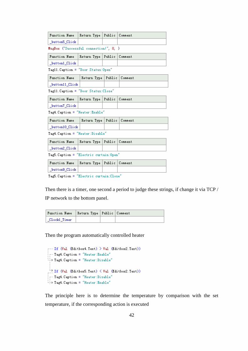
42
Then there is a timer, one second a period to judge these strings, if change it via TCP /
IP network to the bottom panel.
Then the program automatically controlled heater
The principle here is to determine the temperature by comparison with the set
temperature, if the corresponding action is executed

43
The following procedure is automatically controlled electric curtain
Determine the light intensity and temperature determine the procedure similar to the
process, but also through the strength of the current outdoor and indoor intensity
contrast , if the set , it creates action, otherwise perform the opposite action.
This is partly be time to control electric curtains, by comparing the current time and
settings to meet regularly every day on and off electric curtains, and above the light
intensity determine a certain relevance judgments.
Have been written after the code can be compiled out EXE program, and select the
static compilation, refers to the use statically compiled DLL files compiled together
into an EXE , so easy program to run on any computer.
After compilation can be found under the directory with the project name of EXE file,
you can see the user interface of the software, as shown below.

44
Figure 4-5

45
Figure 4-6 The flow chart of application function

46
Chapter 5 - Results
5.1. PCB Design
PCB design is based on the schematics as a basis for the circuit designer to achieve
the required functionality. PCB design layout design mainly refers to the need to
consider the layout of external connections, optimize the layout of internal electronic
components, metal lines, electromagnetic compatibility, heat and other factors.
Excellent PCB design can save production costs, achieve good performance of the
circuit and thermal performance.
PCB layout is to complete one of the most important hardware design step, almost in
front of all the work done in order to better wiring. In the entire of PCB design,
limited to a maximum cabling design work, skill finest, largest workload. Wiring in
two ways: automatic routing and interactive routing. Automatic routing function is
more powerful. It uses interactive routing with automatic routing as the way to
accomplish this design PCB layout. First through interactive routing of important
device wired, such as: power, clock, decoupling capacitors, and other key components,
redesign automatic routing rules, then it can automatic routing, and finally manually
adjust them unreasonable to complete the whole system wiring.

47
Figure 5-1 PCB design
These are the final PCB design. Be in accordance with the ratio of 1:1 on A4 paper
printed. All devices will be placed on the paper contrast, confirm the size is correct,
and then sent to the system board manufacturers.
The below is the physical map of PCB system board.
Figure 5-2 the physical PCB board

48
5.2. Weld and debug
General circuit boards are using tin-lead solder, and its mechanism is: solder during
soldering, welding parts with copper foil under the action of heat during welding,
soldering solder melt and wet surfaces. It rely weldment between the two molecules
move foil. It is causing diffusion between metals. Weldment is formed between the
copper foil and the metal alloy layer. And it achieve to the copper foil and welding
parts together, to obtain a solid solder joint.
Figure 5-3 Magnetic induction module
Figure 5-4 Infrared part module

49
Figure 5-5 Temperature module
Figure 5-6 Light intensity module
Whether the device on the PCB can be used normally, in addition to depending on the
design is correct, there is a big factor in that soldering is correct. Welded to the circuit
board assembly of electronic products has played an important role. The correct spot
welding design and good welding is a key factor in obtaining reliable.
The difficulty lies in the design of welded STM32 chip devices this pin intensive,
specialized welding technicians need to ask welder. All other components are
soldered, as far as possible without weld.

50
Figure 5-7 the physical system board
5.3. Software
5.3.1. Base Driver
Eventually all of the above modules assembled in a whole system, through JLINK
emulator underlying driver to writing into STM32, in order to test each module work.
Figure 5-8 Actual system connection
51
5.3.2. The application
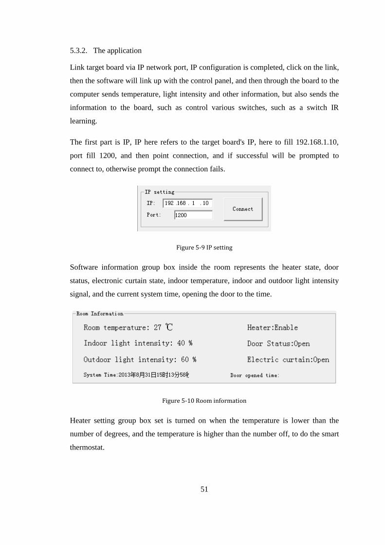
Link target board via IP network port, IP configuration is completed, click on the link,
then the software will link up with the control panel, and then through the board to the
computer sends temperature, light intensity and other information, but also sends the
information to the board, such as control various switches, such as a switch IR
learning.
The first part is IP, IP here refers to the target board's IP, here to fill 192.168.1.10,
port fill 1200, and then point connection, and if successful will be prompted to
connect to, otherwise prompt the connection fails.
Figure 5-9 IP setting
Software information group box inside the room represents the heater state, door
status, electronic curtain state, indoor temperature, indoor and outdoor light intensity
signal, and the current system time, opening the door to the time.
Figure 5-10 Room information
Heater setting group box set is turned on when the temperature is lower than the
number of degrees, and the temperature is higher than the number off, to do the smart
thermostat.

52
Figure 5-11 Heater setting
Electric curtains part here has two parts, one is comparing indoor and outdoor light
intensity, greater than open, less than closure, the other part is to set the time on a
certain time period, in another time period closes.
Figure 5-12 Electric curtains setting
The last one is door timeout setting, if it reaches a setting time, it will warn the user.
Figure 5-13 Door timeout setting
IR learning group box is a learning IR remote control, and in the drop-down menu, it
can be selected the serial number; Then the data corresponds with the button, you can
control the corresponding.
Figure 5-14 IR learning

53
Independent control section, where it can be directly used the software to control the
system board at the switch, skip the judgment part of the program, where you can do
the test, can also be forced on equipment
Figure 5-15 Manual control

54
Chapter 6 - Conclusions and Recommendations
After this time, in the hardware design and software programming and debugging, the
project has achieved some results. Analysis of market research on existing smart
home system, to understand the development and current status of the smart home and
the relevant technology of smart home application. Determine the system design,
select the basic hardware, and determine the system's general functionality. ST's
STM32F103RBT6 selected as the master chip, ENC28J60 is the Ethernet controller
chip. For hardware design, the system is divided into several modules, each module
specifically design the circuit diagram, according to the schematic drawing PCB
board, complete components of the welding. Eventually it is able to carry out the
process of downloading and online debugging. For software design, according to
official libraries with underlying driver design, design the upper application software,
the smart home system through a variety of software to achieve basic application.
The time is limited, currently this project only completed part of the circuit board
design. Also did not achieve more complex functions with the upper application
software development. In the following days, it will have a lot of work to be done. In
the hardware design, first of all, it need to modify the circuit design errors place. But
also to optimize the layout design of the circuit improves strong characterization. This
project can consider adding Wi-Fi and other wireless module, making the smart home
system more feature and perfect. In the mature hardware version, to remove some
debugging tools.
The software is just to achieve some basic application functionality, there is no test of
practical application after a long time. Inevitably there are some unknown bugs.
Meanwhile effort to develop software features is not enough. For each function, there
are many aspects worthy of further and perfected.

55
These works will be continued in subsequent research efforts. If the hardware and
software design to reach maturity level, and strive to be productized. It can be useful
as a low smart home system to enter the market.

56
REFERENCES
1. Hou, Haitao. The development of the smart home. Building Materials
Development. 2004, Vol. 05.
2. Guan, Yong. Industry Development Analysis of the Internet of Things. 2010.
3. Fen, Kai. The origin of the smart home and its development trend. China's new
technology and new products. 06, 2010.
4. Ma, Yumei. The design of household appliances remote control. automation. 05,
2004.
5. Hu, Yi. STM32 programming in the application of the implementation of the
method. Microcontroller and embedded systems applications . 09, 2009.
6. Wang, Tieliu. Based on the STM32 USB data acquisition module design and
implementation. Measurement and control technology. 09, 2009.
7. Zhang, Hainai. The embedded Ethernet interface chip design . Science Technology
and Engineering. 06, 2007.
8. Bai, Tongyun. Research on high-speed PCB Power Integrity. Research Institute of
China Electronics Technology. 01, 2006.
9. Lu, Haifeng. Serial communication based online monitoring system key
technology research. Journal of Scientific Instrument. S3, 2006.
10. Lin, Haifeng. Infrared Transceiver Integrated Circuit Design. Zhejiang University.
2006.
11. Su, Qi. ARM core-based microcontrollers Minimum System Design and
Implementation. Tianjin University. 2004.

57
12. Wang, Xiangting. STM32-based wireless intelligent home control system.
Automation and Applications. 08, 2011.
13. Xu, Fangrong. Wireless Intelligent Home Control System Design. Modern
building electrical. 01, 2010.
14. Chen, Jian. Remote network technology based smart home system. Technology
Square. 10, 2005.
15. Du, Tao. Intelligent Home Control System Design and Implementation.
Automation and Applications. 02, 2010.
16. Ge, Nianming. Based on the STM32 Development Application System Design .
Micro computer and application . 17, 2012.
17. Sun, Jing. Research and realization of the smart home controller based on
Ethernet . Xian university of science and technology. 2006.
18. Jie, Zhaoyan. Based on embedded system network design and implementation of
the smart home controller . Shandong university of science and technology. 2006.

58
APPENDICES
1. Base Driver: Infrared part module

59

60
2. Base Driver: Temperature module

61

62
3. The application of the smart home system
63