experiment 2 impedance and frequency...
TRANSCRIPT

Introductory Electronics Laboratory
2-i
Experiment 2 Impedance and frequency response
The first experiment has introduced you to some basic concepts of analog circuit analysis and amplifier design using the “ideal” operational amplifier along with a few resistors and operating at low frequencies. To make further progress we need to add a couple of powerful tools for understanding and describing the behavior of our analog circuits: the concepts of impedance and frequency response. These ideas live in the frequency-domain — that world of “eternal” sinusoidal waves which is the Fourier transform space of our circuits’ time-varying voltages and currents. Once we understand these new ideas we can add capacitors to our op-amp circuit designs, greatly expanding the usefulness of our growing repertory.
We will represent the amplitude and phase of any given sinusoid as a vector in a plane. We can express and manipulate this vector as a complex number called a phasor. This phasor representation of a sinusoid (which is a single complex number) is the Fourier transform of the oscillating signal and “lives” in the frequency-domain. The powerful advantages of this technique result because linear differential equations of time become complex-valued algebraic expressions of frequency in this transformed, Fourier space. For example, as we shall see, the capacitor and inductor circuit elements have voltage-current relationships in the frequency-domain which look like the resistor’s Ohm’s law. Thus we arrive at the concept of complex-valued impedance as a generalization of resistance which can include the effects of these additional circuit elements.
Voltage dividers which include capacitors with resistors have transfer functions which usually vary with frequency. This sort of variation defines the frequency response of a circuit or network, which can be graphically displayed using a Bode plot. We can use a circuit’s frequency response to predict how it will respond to abrupt changes in its inputs, which leads to the related concepts of transient response and settling time. Designing a circuit to only pass signals within a specified frequency range leads to the concept of a filter.
It turns out that these ideas also provide the tools we need to more thoroughly study the behavior of a real operational amplifier circuit, which can only approximate the ideal op-amp. We will see how our actual amplifier circuits have frequency limitations which depend on their gains; we also learn how to design amplifiers which can integrate or differentiate their time-varying inputs. By the end of this experiment you will be able to design circuits which can apply a linear, integro-differential operator to an input signal — a basic building block of the analog computer and the PID (proportional-integral-differential) feedback controller.

Experiment 2
2-ii
Copyright © Frank Rice 2014-2019
Pasadena, CA, USA
All rights reserved.

Introductory Electronics Laboratory
2-iii
CONTENT S
TABLE OF CIRCUITS 2-V
CAPACITORS AND INDUCTORS 2-1 Capacitors ...................................................................................................................................................... 2-1 The RC time constant ..................................................................................................................................... 2-3 Inductors ........................................................................................................................................................ 2-4 Warnings ....................................................................................................................................................... 2-6
FREQUENCY-DOMAIN REPRESENTATIONS 2-8 Representing a sinusoidal waveform as a complex number: the phasor ...................................................... 2-8 Time-domain and frequency-domain representations ................................................................................ 2-10 The actions of linear functions on the representations............................................................................... 2-12
EXTENDING OHM’S LAW: IMPEDANCE 2-15 Parallel RC impedance vs. frequency ........................................................................................................... 2-16 RC voltage dividers as simple filters ............................................................................................................. 2-17 AC coupling using the RC high-pass filter: blocking a DC signal component ............................................... 2-20
THE REAL, FINITE-GAIN OP-AMP 2-22 Approximating the ideal: the real op-amp frequency response .................................................................. 2-22 Frequency responses of real amplifier circuits ............................................................................................. 2-23
SKETCHING BODE PLOTS OF SIMPLE CIRCUITS 2-27 Series and parallel combinations ................................................................................................................. 2-27 Voltage dividers ........................................................................................................................................... 2-29 Sketching complex-valued frequency response expressions ........................................................................ 2-31
THE TRANSIENT RESPONSE OF A SIMPLE FILTER 2-33
INTEGRATORS AND DIFFERENTIATORS 2-35 Basic integrator and differentiator circuits .................................................................................................. 2-35 A practical integrator circuit ........................................................................................................................ 2-35 The practical op-amp differentiator ............................................................................................................ 2-37
PRELAB EXERCISES 2-40
LAB PROCEDURE 2-41 Gain-bandwidth product limitations of op-amp amplifiers ......................................................................... 2-41 Transient Response ...................................................................................................................................... 2-42 Adding AC coupling to an amplifier input .................................................................................................... 2-42 Additional, self-directed investigations ....................................................................................................... 2-43 Lab results write-up ..................................................................................................................................... 2-43
MORE CIRCUIT IDEAS 2-44 Phase shifter (all-pass filter) ........................................................................................................................ 2-44 AC coupled inverting amplifier ..................................................................................................................... 2-44 High input impedance, high gain, inverting amplifier ................................................................................. 2-45
ADDITIONAL INFORMATION ABOUT THE TEXT IDEAS AND CIRCUITS 2-47

Experiment 2
2-iv
Quick review of complex numbers ............................................................................................................... 2-47 Fourier and Laplace transforms ................................................................................................................... 2-49 Power dissipation calculations using phasors .............................................................................................. 2-51 Transformers ................................................................................................................................................ 2-51 Mitigating DC offset errors in high-gain circuits .......................................................................................... 2-54 Instrument input impedance and cable capacitance issues......................................................................... 2-56 The 10x Oscilloscope probe .......................................................................................................................... 2-59

Introductory Electronics Laboratory
2-v
TABLE OF C IRCUIT S
Amplifier, AC coupled input, noninverting 2-20
Amplifier, AC coupled input, inverting 2-45
Amplifier, high-gain inverting configuration 2-46
Amplifier, input offset error compensated 2-55
Buffer amplifier, long cable 2-58
Differentiator, inverting, basic 2-35
Differentiator, inverting, resistor damping 2-38
Filter, all-pass (phase shifter) 2-44
Filter, RC low-pass or high-pass 2-17
Integrator, inverting, basic 2-35
Integrator, inverting, DC gain limited 2-36
Instrument input models 2-56
10× oscilloscope probe 2-59

Introductory Electronics Laboratory
2-1
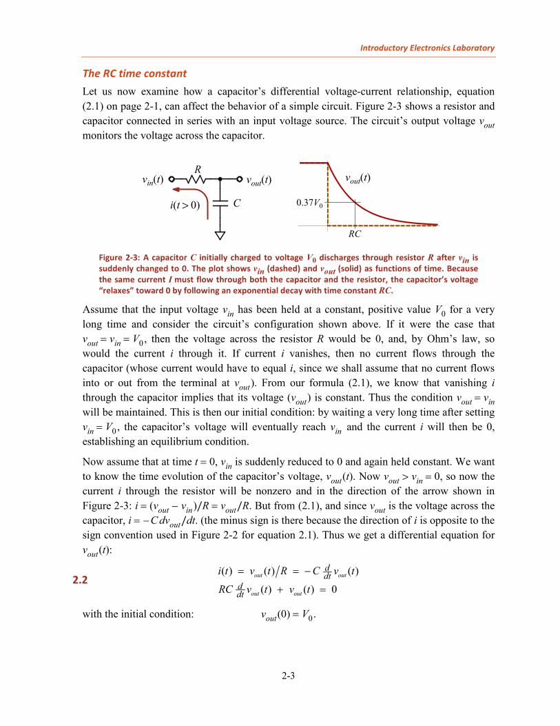
CAPACIT ORS AND INDUCT ORS Capacitors Several capacitors are shown in Figure 2-1 on page 2-2. Conceptually, a capacitor consists of two conductive surfaces separated by a thin insulator, and each conductive surface is connected to a terminal of the device (shown in Figure 2-2 on page 2-2, the schematic symbol for a capacitor is suggestive of this arrangement). As current flows through a capacitor, charge builds up on one surface while an equal and opposite charge accumulates on the other; the total charge of the element remains 0. The resultant electric field between the surfaces creates a potential difference (voltage) between them and, consequently, the two terminals of the capacitor. This voltage difference is proportional to the amount of charge stored on each of the capacitor’s conductive surfaces. The rate of change of the charge on each surface is proportional to the current flowing through the capacitor. The relation between current and voltage for a capacitor is therefore a differential one, as shown in equation (2.1) and Figure 2-2.
2.1 Capacitor: ( ) ( )ddti t C v t=
The constant of proportionality, C, is called capacitance and has the SI unit Farad: 1 farad 1 amp/(volt/sec) 1 coulomb/volt 1 sec/ohm.= = = An ideal capacitor has a value for its capacitance C which is a constant, nonnegative real number, independent of voltage, current, or frequency. Equation (2.1) is the defining relation for an ideal capacitor, and the actual capacitors you will use can behave in a reasonably ideal manner as long as you are careful with them; capacitors having values of less than about 0.1 microfarad (μF or uF, 10−6 F) generally behave in a very nearly ideal manner.
The relation between the current and voltage of a capacitor (equation 2.1) is the same whether we control the current through it and measure its resulting voltage, or control its voltage and ask what the current must be. Thus, if the voltage across a capacitor is constant, the current through it must vanish. Conversely, rapid changes in a capacitor’s voltage require large currents to change its charge: the higher the capacitance, the larger the current required. Discharging a large-valued capacitor with a high-conductivity wire can have a spectacular but dangerous result!
Because the insulating layers separating the conductive surfaces in a large-valued capacitor can be very thin, too high a voltage across it can subject it to damage from internal electrical discharge (a spark). The higher the capacitance required, the lower the voltage limit for a capacitor of a given physical size. This is the primary driver of the sizes of the capacitors shown in Figure 2-1. Each capacitor has a maximum voltage limit which may be written on the capacitor body. As the voltage across the capacitor approaches this limit, its behavior usually becomes much less ideal, and equation (2.1) could be quite inaccurate in this case.

Experiment 2: Capacitors and Inductors
2-2
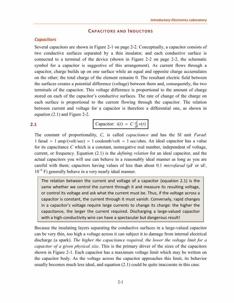
Another consideration when choosing a capacitor is the nature of the insulator it employs. To get large capacitances, a manufacturer may choose to chemically deposit extremely thin insulating layers using electrolysis. Because this chemical process may be inadvertently reversed by you, the user, these electrolytic capacitors must be used correctly! Electrolytic capacitors have an inherent polarity; the voltage across such a capacitor must never have the opposite polarity, or it could be permanently damaged. If you look carefully at Figure 2-1 you can see the polarity markings on the electrolytic capacitors — the very large one in the figure and the one right below it.
A farad (F) is a very large capacitance. The most useful capacitor range for our designs is within a couple of orders of magnitude of a nanofarad (nF, 910− F). Capacitances of more than a few microfarads usually require an electrolytic capacitor. An electrolytic capacitor is denoted in a schematic by a symbol with a polarity mark (+) as shown at right.
LARGE-VALUED CAPACITORS ARE FAR FROM IDEAL Large capacitors (with values exceeding about 1μF) tend to behave in a less than ideal manner at high frequencies, especially if they are electrolytic. If you need a large value of capacitance but also need it to work well at high frequencies (above 1MHz), then you should place a smaller-valued capacitor (10–100nF) in parallel with the larger one.
Figure 2-1 (left): A variety of capacitors, from the tiny (.08 inch × .05 inch) surface-mount component barely visible near the left side of the photo (see arrow) to the soda-can-sized power supply filter capacitor dominating the scene. The small, orange capacitor just to the right of the surface-mount device is a multi-layer ceramic type like you will mostly use for your designs.
Figure 2-2 (right): A simple circuit illustrating the differential voltage-current relation for a capacitor with value C. Note the use of a current source to drive the capacitor in this case. Also shown are the usual conventions for the polarity of the change in voltage and direction of the current flow when the current i( t) > 0 .
( )i t ( )i t( )v t+
–
( ) ( )ddti t C v t= ×
Introductory Electronics Laboratory
2-3
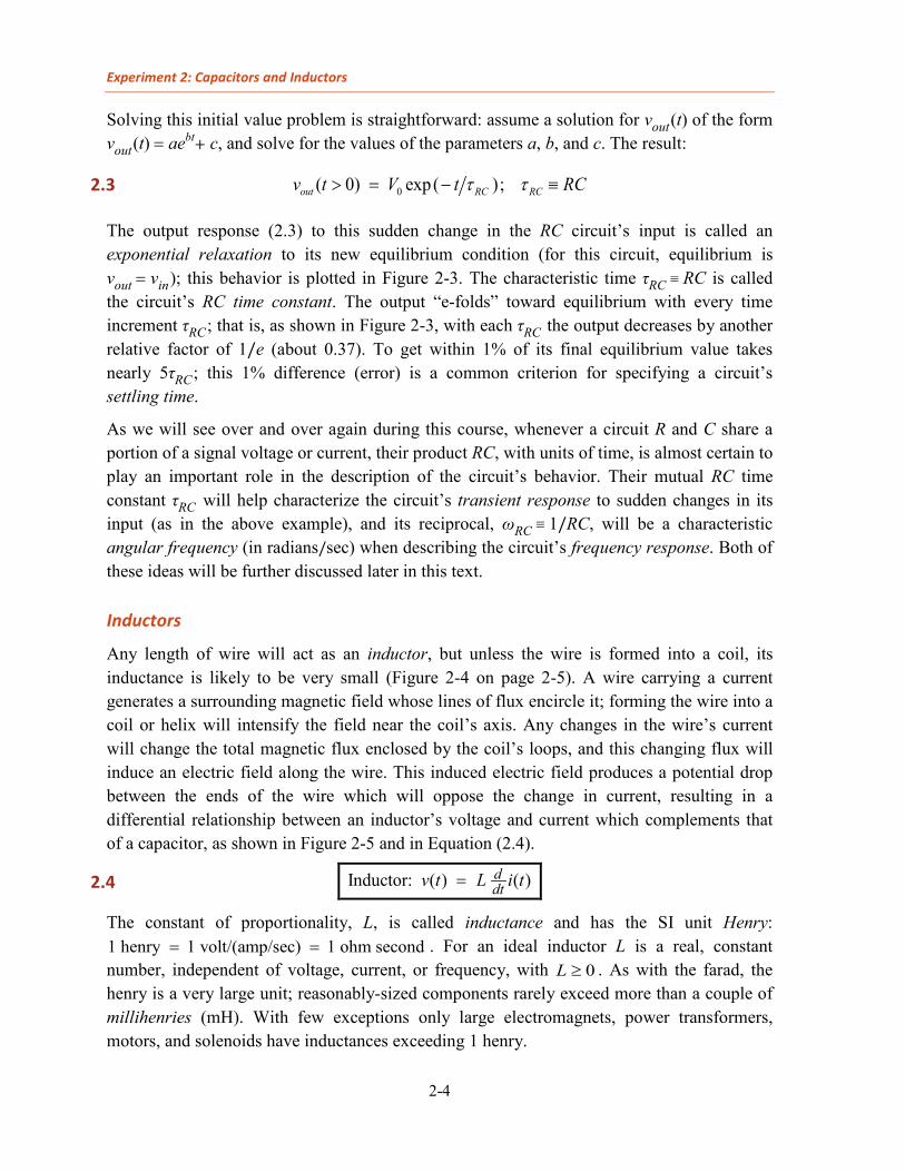
The RC time constant Let us now examine how a capacitor’s differential voltage-current relationship, equation (2.1) on page 2-1, can affect the behavior of a simple circuit. Figure 2-3 shows a resistor and capacitor connected in series with an input voltage source. The circuit’s output voltage vout monitors the voltage across the capacitor.
Figure 2-3: A capacitor C initially charged to voltage V0 discharges through resistor R after vin is suddenly changed to 0. The plot shows vin (dashed) and vout (solid) as functions of time. Because the same current I must flow through both the capacitor and the resistor, the capacitor’s voltage “relaxes” toward 0 by following an exponential decay with time constant RC.
Assume that the input voltage vin has been held at a constant, positive value V0 for a very long time and consider the circuit’s configuration shown above. If it were the case that vout = vin = V0, then the voltage across the resistor R would be 0, and, by Ohm’s law, so would the current i through it. If current i vanishes, then no current flows through the capacitor (whose current would have to equal i, since we shall assume that no current flows into or out from the terminal at vout). From our formula (2.1), we know that vanishing i through the capacitor implies that its voltage (vout) is constant. Thus the condition vout = vin will be maintained. This is then our initial condition: by waiting a very long time after setting vin = V0, the capacitor’s voltage will eventually reach vin and the current i will then be 0, establishing an equilibrium condition.
Now assume that at time t = 0, vin is suddenly reduced to 0 and again held constant. We want to know the time evolution of the capacitor’s voltage, vout(t). Now vout > vin = 0, so now the current i through the resistor will be nonzero and in the direction of the arrow shown in Figure 2-3: i = (vout − vin)/R = vout/R. But from (2.1), and since vout is the voltage across the capacitor, i = −C dvout/dt. (the minus sign is there because the direction of i is opposite to the sign convention used in Figure 2-2 for equation 2.1). Thus we get a differential equation for vout(t):
2.2 ( ) ( ) ( )
( ) ( ) 0out out
out out
ddt
ddt
i t v t R C v t
RC v t v t
= = −
+ =
with the initial condition: vout(0) = V0.
i(t > 0)
vin(t) vout(t)
C
Rvout(t)
RC
0.37V0
Experiment 2: Capacitors and Inductors
2-4
Solving this initial value problem is straightforward: assume a solution for vout(t) of the form vout(t) = aebt+ c, and solve for the values of the parameters a, b, and c. The result:
2.3 0( 0) exp( );out RC RCv t V t RCt t> = − ≡
The output response (2.3) to this sudden change in the RC circuit’s input is called an exponential relaxation to its new equilibrium condition (for this circuit, equilibrium is vout = vin); this behavior is plotted in Figure 2-3. The characteristic time τRC ≡ RC is called the circuit’s RC time constant. The output “e-folds” toward equilibrium with every time increment τRC; that is, as shown in Figure 2-3, with each τRC the output decreases by another relative factor of 1/e (about 0.37). To get within 1% of its final equilibrium value takes nearly 5τRC; this 1% difference (error) is a common criterion for specifying a circuit’s settling time.
As we will see over and over again during this course, whenever a circuit R and C share a portion of a signal voltage or current, their product RC, with units of time, is almost certain to play an important role in the description of the circuit’s behavior. Their mutual RC time constant τRC will help characterize the circuit’s transient response to sudden changes in its input (as in the above example), and its reciprocal, ωRC ≡ 1/RC, will be a characteristic angular frequency (in radians/sec) when describing the circuit’s frequency response. Both of these ideas will be further discussed later in this text.
Inductors
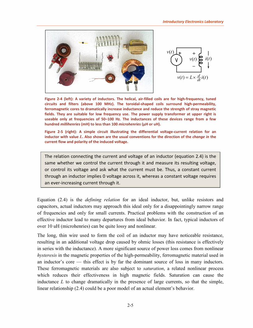
Any length of wire will act as an inductor, but unless the wire is formed into a coil, its inductance is likely to be very small (Figure 2-4 on page 2-5). A wire carrying a current generates a surrounding magnetic field whose lines of flux encircle it; forming the wire into a coil or helix will intensify the field near the coil’s axis. Any changes in the wire’s current will change the total magnetic flux enclosed by the coil’s loops, and this changing flux will induce an electric field along the wire. This induced electric field produces a potential drop between the ends of the wire which will oppose the change in current, resulting in a differential relationship between an inductor’s voltage and current which complements that of a capacitor, as shown in Figure 2-5 and in Equation (2.4).
2.4 Inductor: ( ) ( )ddtv t L i t=
The constant of proportionality, L, is called inductance and has the SI unit Henry: 1 henry 1 volt/(amp/sec) 1 ohm second= = . For an ideal inductor L is a real, constant number, independent of voltage, current, or frequency, with 0L ≥ . As with the farad, the henry is a very large unit; reasonably-sized components rarely exceed more than a couple of millihenries (mH). With few exceptions only large electromagnets, power transformers, motors, and solenoids have inductances exceeding 1 henry.
Introductory Electronics Laboratory
2-5
The relation connecting the current and voltage of an inductor (equation 2.4) is the same whether we control the current through it and measure its resulting voltage, or control its voltage and ask what the current must be. Thus, a constant current through an inductor implies 0 voltage across it, whereas a constant voltage requires an ever-increasing current through it.
Equation (2.4) is the defining relation for an ideal inductor, but, unlike resistors and capacitors, actual inductors may approach this ideal only for a disappointingly narrow range of frequencies and only for small currents. Practical problems with the construction of an effective inductor lead to many departures from ideal behavior. In fact, typical inductors of over 10 uH (microhenries) can be quite lossy and nonlinear.
The long, thin wire used to form the coil of an inductor may have noticeable resistance, resulting in an additional voltage drop caused by ohmic losses (this resistance is effectively in series with the inductance). A more significant source of power loss comes from nonlinear hysteresis in the magnetic properties of the high-permeability, ferromagnetic material used in an inductor’s core — this effect is by far the dominant source of loss in many inductors. These ferromagnetic materials are also subject to saturation, a related nonlinear process which reduces their effectiveness in high magnetic fields. Saturation can cause the inductance L to change dramatically in the presence of large currents, so that the simple, linear relationship (2.4) could be a poor model of an actual element’s behavior.
Figure 2-4 (left): A variety of inductors. The helical, air-filled coils are for high-frequency, tuned circuits and filters (above 100 MHz). The toroidal-shaped coils surround high-permeability, ferromagnetic cores to dramatically increase inductance and reduce the strength of stray magnetic fields. They are suitable for low frequency use. The power supply transformer at upper right is useable only at frequencies of 50–100 Hz. The inductances of these devices range from a few hundred millihenries (mH) to less than 100 microhenries (μH or uH).
Figure 2-5 (right): A simple circuit illustrating the differential voltage-current relation for an inductor with value L. Also shown are the usual conventions for the direction of the change in the current flow and polarity of the induced voltage.
( )i t( )v t+
–
( ) ( )ddtv t L i t= ×
( )v t
Experiment 2: Capacitors and Inductors
2-6
Warnings To stay safe, you must be cautious when using large-valued capacitors and inductors (including transformers). Please take heed:
WARNING: Rapid changes in the current through an inductor can result in extremely large induced voltages as its magnetic field changes. This is especially worrisome should the current through an inductive device (such as an electromagnet, solenoid, or relay) be suddenly interrupted — induced voltages of hundreds and even thousands of volts may be generated, causing extensive circuit damage and even lethal shocks.
A large electromagnet can be especially dangerous: the high current needed to generate its intense field can store a lethal amount of energy in the surrounding magnetic flux. Suddenly interrupting the magnet’s power supply can induce a deadly pulse of current driven by a very high voltage into any nearby conductors, including people.
WARNING: Some large capacitors have very high operating voltages and can store many joules of electrical energy. Even when disconnected from a circuit, a well-designed capacitor can store this energy and maintain the high voltage between its two terminals for years! In this case touching one of the terminals could kill you! Particularly sinister culprits are old cathode-ray tube (CRT) monitors and televisions. Even CRT devices which haven’t been used for a decade or longer can contain circuitry with charged capacitors connected to transformers which can generate several tens of thousands of volts: don’t touch!
Finally, I must mention less serious problems caused by stray capacitance: they may not kill you, but they can result in severe headaches as you struggle to troubleshoot a poorly-designed circuit which ignored their effects:
STRAY CAPACITANCE Inadvertent capacitance exists between any two conductors (wires) which are close to each other, and this fact has plagued many a beginning circuit designer and builder! Any two nearby wires form a small capacitor of about a picofarad per centimeter of wire length (pF, 1210− F). As a result, high-frequency signals may be transferred though this capacitance, effectively connecting the wires’ circuitry. This unfortunate fact is what will limit the useful frequencies of our breadboard circuits to no more than about 10 MHz.

Introductory Electronics Laboratory
2-7
To keep these stray capacitances from spoiling your project, you shouldn’t use a circuit design which requires capacitor values of less than about 33 pF (or even more, to stay on the safe side).
STRAY CAPACITANCE BETWEEN INDUCTOR WINDINGS One of the more serious problems plaguing a real inductor is that its closely-spaced turns of wire have a stray capacitance coupling them. This capacitance is effectively in parallel with the element’s inductance, so at high frequencies the oscillating voltage difference between adjacent windings will produce a current that bypasses the desired flow around each winding. Thus at high frequencies its magnetic field can be greatly reduced, making a coil behave more like a capacitor than an inductor! This change from predominantly inductive to capacitive behavior is usually quite abrupt as frequency is increased through the inductor’s self-resonant frequency. Because closely-spaced windings of thin wire have higher stray capacitance and result in lower self-resonant frequencies, inductors designed for high-frequency use avoid this design (look again at the high-frequency inductors in Figure 2-4). You will investigate the important phenomenon of resonance in a later experiment.

Experiment 2: Frequency-domain Representations
2-8
FREQUENCY-DOMAIN REPRESENT ATIONS
Representing a sinusoidal waveform as a complex number: the phasor Let us see how a sinusoidal function of time can be thought of as a vector in a plane. Consider the simple function ( ) cos( ),x aθ θ= plotted in the figure at right (we assume that any angle used as an argument to a function will be expressed in radians). This function could then be the x-component of a 2-D vector function A(θ ) with magnitude a and angle θ measured counter-clockwise from the positive x-axis, as shown in the lower figure (a polar coordinate representation of A). As θ is varied, the vector A(θ ) rotates around the origin. We will call the angle θ the instantaneous phase (or, more simply, the phase) of the functions x(θ ) and A(θ ).
Our signals will have phases which are functions of time: θ = θ (t ). For a simple sinusoidal signal the function will be ( ) cos( ),x t a tω φ= + where ω is the wave’s angular frequency (in radians/sec or, equivalently, sec−1). Then ω = 2π f , with the frequency f measured in the more traditional cycles/sec or hertz (Hz; also kHz for 103 Hz, MHz for 106 Hz).
We will use “f ” rather than the Greek “ν” to represent frequencies in hertz, i.e. cycles/sec, so that there is no confusion with a voltage v(t); the Greek “ω” will, as usual, represent angular frequencies (in radians/sec, i.e. sec–1).
To remember the correct place to put the 2π when converting between ω and f, just remember its units: 2π radians/cycle.
ω will be larger than the corresponding f : 2π ≈ 6; 1/2π ≈ 0.16.
The angle ϕ in cos( )tω φ+ is called the signal’s phase shift and gives its phase when t = 0. If the signal’s phase shift is greater than 0, then we say that the signal’s phase leads the phase of cos ωt because it reaches any given phase angle θ at an earlier time; if 0φ < the signal’s phase lags that of cos ωt. Our fiducial phase reference signal will be this function cos ωt. Using our vector model, it will be represented by the x-axis projection of a vector with unit length rotating counter-clockwise at the constant angular rate ω, a vector we will call ˆ( ).tθ At time t = 0 the vector ˆ(0)θ coincides with the unit x-coordinate vector, x . Similarly, at time t = 0 our waveform ( ) cos( )x t a tω φ= + can be represented by a vector A(0) of length a and phase angle ϕ; A(t) then rotates with time at the rate ω because of the ωt term, maintaining
θ
x(θ)
cos( )xa θ
=θ
a
A(θ)sin( )y a θ=
Introductory Electronics Laboratory
2-9
the constant angle ϕ away from ˆ( ).tθ Again, to get the actual function x(t) we take the projection of A(t) onto the x-axis, say by using a vector dot product: ˆ( ) ( ).x t t= ⋅x A
At first this idea of using the projection of a rotating vector to represent the sinusoid x(t) seems unnecessarily complicated. In fact, this representation can lead to a great simplification of the mathematics! We will extend our definition of numbers and simple operations such as multiplication to include and manipulate these geometric (2-D vector) representations of our signal’s amplitude and phase. This mapping between vectors and numbers was introduced by the great 18th century Swiss mathematician and physicist Leonhard Euler.
To motivate this paradigm shift, we note that life would be easier if we could somehow factor out the cyclic ωt variation of our sinusoids, because what really differentiates any two sinusoids with the same frequency are their amplitudes and phase shifts (a’s and ϕ’s). In other words, continuing the discussion above, we want to find a way of representing our vectors A(t) and ˆ( )tθ so that ˆ( ) (0) ( ).t t=A A θ Then we can just represent the sinusoid with the static vector A(0) with length a and phase angle ϕ; at the end we could just multiply by ˆ( )tθ and take the result’s x-component to get back the sinusoid cos( ).a tω φ+ But how to make this work? Consider the trigonometry of ˆ(0) ( ) :tA θ
ˆ ˆ(0) cos( ) sin( )
ˆ ˆ ˆ( ) cos( ) sin( )ˆ ˆ( ) cos( ) sin( )
a at t tt a t a t
φ φω ω
ω φ ω φ
= +
= += + + +
A x yθ x yA x y
but
cos( ) cos( )cos( ) sin( )sin( )sin( ) cos( )sin( ) sin( )cos( )
t t tt t t
ω φ φ ω φ ωω φ φ ω φ ω
+ = −+ = +
whereas, formally, the product
[ ][ ][ ]
[ ]
ˆ ˆ ˆ ˆ ˆ(0) ( ) cos( ) sin( ) cos( ) sin( )ˆ ˆ ˆ ˆcos( )cos( ) sin( )sin( )
ˆ ˆcos( )sin( ) sin( )cos( )
t a a t ta t t
a t t
φ φ ω ωφ ω φ ω
φ ω φ ω
= + +
= +
+ +
A θ x y x yxx yy
xy
We haven’t yet defined how we’re supposed to interpret the products of the unit vectors in this last expression. To get our desired result ˆ( ) (0) ( ),t t=A A θ we require that ˆ ˆ ˆ=xx x and ˆ ˆ ˆ ,=xy y but ˆ ˆ ˆ.= −yy x Euler’s insight was to interpret these expressions as ordinary multiplications of numbers, identifying ˆ 1↔x and then ˆ 1 ,j↔ − ≡y so our 2-D vectors can be identified with complex numbers for the purposes of representing our sinusoids! Since ˆ 1,↔x the x-axis represents ordinary, real numbers; conversely the y-axis represents pure imaginary numbers. With this identification, the vector A(0) becomes the complex number
(cos sin ).A a jφ φ= +
Experiment 2: Frequency-domain Representations
2-10
We will use 1j ≡ − rather than Euler’s “i.” We do this to avoid confusion with the symbol for a current i(t). This is standard electrical engineering practice, and is the convention used by nearly all electronics texts).
We will generally use upper-case letters (“Z”, “Y ”, “W”) to represent complex-valued numbers and functions (usually functions of frequency), while lower-case letters shall be reserved for real-valued functions (usually of time). Obvious exceptions will be to use R, L, and C to represent real-valued resistance, inductance, and capacitance.
Because our complex number A corresponding to the vector A(0) was formed from the magnitude a and phase shift ϕ of a sinusoid, we call it a phasor or complex amplitude. The x-component of the vector A(0) corresponds to the real part of the phasor A, Re[ ] cos ,A a φ= and its y-component to the imaginary part of A: Im[ ] sin .A a φ= The real and imaginary parts of the complex-valued phasor A thus provide the Cartesian components of A(0).
The pair a and ϕ themselves of course provide a polar-coordinate representation (magnitude and orientation angle) of A(0). Using the multiplication scheme outlined above for our complex representation of ˆ( ) (0) ( ),t t=A A θ it is evident that in terms of their polar coordinate representations, the magnitude of the product of two complex numbers is the product of their magnitudes, whereas the phase of the product is the sum of their phases. Euler accommodated this property by his identification of phase with the exponent of a complex number through his brilliant definition of complex exponentiation,
cos( ) sin( )je jφ φ φ≡ +
providing a quite useful, polar representation of the complex number A: .jA a e φ= Its reciprocal would then be 1 (1 ) ,/ jA a e φ− −= and, in particular, j −1
= – j.
The complex number representation of ˆ( )tθ becomes ,j te ω and therefore A(t) is represented by ( ).j t j tAe a eω ω φ+= A more comprehensive summary of the elementary mathematics of complex numbers is provided in the section Quick review of complex numbers starting on page 2-47.
Time-domain and frequency-domain representations To summarize the previous section, we can represent a sinusoidal function of time (such as an AC voltage or current) using complex numbers:
2.5 If: ( ) cos ( )
then: ( ) Re ; where j t jx t a t
x t Ae A a eω φω φ= +
= =
Introductory Electronics Laboratory
2-11
As we stated previously, the complex number A is called a phasor since it specifies both the amplitude a and phase ϕ of x(t). If the phase of A is greater than 0, then the phase of x(t) leads the phase of cos tω ; if 0φ < the phase lags that of cos tω .
A sinusoid x(t) with the functional form assumed in (2.5) has an associated phasor A which is not a function of time t, because in (2.5) all time dependence of x(t)’s complex representation is captured in its j te ω factor. In practice what this means is that we must wait long enough after energizing the circuit or making adjustments to it for its behavior to settle down and reach steady-state. Once this condition has been achieved, then our phasor model of x(t) is accurate and will continue to work until we make some future change. If our circuit behaves linearly (as defined in Experiment 1) and we have just a single, sinusoidal input with angular frequency ω = 2π f , then all time-varying voltages and currents in the circuit will also vary sinusoidally at the same frequency (possibly plus some constant, DC values). Thus all may be represented by phasors multiplied by the common factor j te ω as in (2.5).
Under the conditions outlined above, we will usually find that, even though our circuit is linear, the amplitudes and phases of the phasors specifying the various circuit voltages and currents will change if we vary the input signal’s angular frequency ω (of course waiting long enough after each frequency change for the circuit to again achieve steady state). The various sinusoidal circuit voltages v1(t), v2(t), etc., and currents i1(t), i2(t), etc., must therefore be represented by phasors which are functions of ω: V1(ω), V2(ω), …, I1(ω), I2(ω), etc. In fact it will generally be the case that any particular phasor A = A(ω), that is, its magnitude and phase can be expected to be functions of frequency.
When we consider complex-valued phasors as specifications of real-valued, sinusoidal functions of time we are using a frequency-domain representation of the functions, working in the Fourier transform space of the corresponding functions of time. The essence of the correspondence between these alternative representations is illustrated by equations (2.5).
The mathematics of the Fourier transform and the relationship between time-domain and frequency-domain representations is explored in more detail in the section

Experiment 2: Frequency-domain Representations
2-12
Fourier and Laplace transforms starting on page 2-49.
The actions of linear functions on the representations
In this section we discuss some fairly abstract mathematics which will nevertheless be important for you to understand. A typical circuit will take some input y(t) and generate some output in response. We describe this relationship using a transfer function as introduced in Experiment 1. How does the operation of a linear transfer function on some time-varying input signal y(t), producing output z(t), look in the frequency-domain? In other words, given a linear circuit with input y(t) and corresponding output z(t), related by the linear, real-valued operation z(t) = g[y(t)], then how will the corresponding phasor representations Y(ω) of y(t) and Z(ω) of z(t) be related? That is, what will be the Fourier-transform of operation g[ ], Z(ω) = G[Y(ω)]? What about the inverse transform? If we know how a circuit operates on input phasors at various frequencies to generate output phasors Z(ω) = G[Y(ω)], can we calculate the time-domain functional relationship between some arbitrary input and the circuit’s output, z(t) = g[y(t)]?
A linear function operating on a single argument is defined as follows: If its argument is composed of a linear combination of several terms, then the resulting function value will be an identical combination of the function’s values when operating individually on each of the terms:
for linear g[] and constants a and b: 1 2 1 2[ ( ) ( )] [ ( )] [ ( )]g ay t by t a g y t b g y t+ = +
The two prototypical linear operations on y(t) are: (1) multiplying by a constant, and (2) taking a time derivative. All linear operations on y(t) will consist of a combination of sums and compositions of these two prototypes and their inverses (interestingly, simply adding a constant to y(t) is not a linear operation, because, for example, doubling the amplitude of y(t) would not then in general double the result). Note that the transformation (2.5) between a sinusoid y(t) and its phasor Y(ω) is itself a linear operation, and so is a sum of such terms (one for each sinusoid in a composite signal, say). Since the composition of two linear operations results in another linear operation, we immediately know that a linear operation g [y(t)] will transform to a corresponding linear operation in the frequency-domain G [Y(ω)]. The problem is to determine the correspondence between these two operations g and G.
The simplest linear operation, multiplying by a constant, is trivially easy to handle. A cursory glance at equation (2.5) should make it obvious that multiplying (or scaling) y(t) by some (real-valued) constant a will simply result in scaling Y(ω) by the same constant:
2.6 ( ) ( ) ( ) ( )y t a y t Y aY→ ⇔ →ω ω (a real, constant)

Introductory Electronics Laboratory
2-13
Multiplying Y(ω) by some complex-valued constant ZjZ z e φ= , on the other hand, corresponds to changing both the amplitude and phase of y(t) (consider equations (2.5)):
2.7 ( ) ( ) ( ) cos( ) ( ) cos( )ZY Z Y y t a t y t za tω ω ω φ ω φ φ→ ⇔ = + → = + +
Taking a time derivative of y(t) has a straightforward and quite simple effect on Y(ω). Consider equations (2.5), in which y(t) is a simple sinusoid. In this case we can evaluate the derivative as it operates on both sides of the second equation of (2.5), keeping in mind that the order of time differentiation and taking the real part may be reversed (see page 2-48):
( ) Re ( ) Re ( ) Re ( )j t j t j td d dy t Y e Y e j Y edt dt dt
ω ω ωω ω ω ω = = =
Thus, taking a time derivative of a function y(t) corresponds to simply multiplying its frequency-domain representation Y(ω) by jω. This result obtains even for some arbitrary y(t) requiring a more complicated Fourier integral representation (see the text describing equations (2.31) on page 2-49).
2.8 ( ) ( ) ( ) ( )dy t y t Y j Ydt
ω ω ω→ ⇔ →
Similarly, dividing Y(ω) by jω corresponds to an integration of y(t). This important result shows that linear differential equations of time when transformed will become complex polynomial equations of frequency.
This result (2.8) will be critical for our extension of Ohm’s law to include capacitors and inductors. For example, let’s return to the circuit example from the previous section The RC time constant on page 2-3. In that example we considered the voltage across the capacitor of a series-connected RC circuit (Figure 2-3). The differential equation (2.2) we derived to describe the circuit’s behavior is repeated below, except that we won’t substitute vin = 0:
2.9 ( ) ( ( ) ( )) ( )
( ) ( ) ( )out in out
out out in
ddt
ddt
i t v t v t R C v t
RC v t v t v t
= − = −
+ =
Let’s convert this final differential equation relating vin(t) and vout(t) to its frequency-domain representation relating the corresponding phasors Vin(ω) and Vout(ω). Using (2.6), the constant RC transfers intact to the new representation, whereas the time derivative of vout(t), using (2.8), becomes jωVout(ω):
2.10 ( ) ( ) ( )
1( ) ( )1
out out in
out in
j RC V V V
V Vj RC
ω ω ω ω
ω ωω
+ =
=+
This new algebraic expression relates input and output phasors: in other words, it describes the output sinusoid Vout’s amplitude and phase when the circuit is driven by an input sinusoid
Experiment 2: Frequency-domain Representations
2-14
Vin(ω). As we will see in the next section, we could have derived this expression directly using frequency-domain interpretations of Ohm’s law and Kirchhoff’s laws.

Introductory Electronics Laboratory
2-15
EXT ENDING OHM’S LAW: IMPEDANCE With our powerful frequency-domain and phasor arsenal at our disposal we consider again the voltage-current relationships for the three basic, two-terminal elements: resistor, capacitor, and inductor. Equations (2.5) or, more generally, (2.31) define the relationships of the complex-valued voltage and current phasor representations V(ω) and I(ω) to their time-varying counterparts v(t) and i(t) across and through an element. Using the operator transformations of the previous section we now express the various voltage-current laws for our elements in terms of the phasor representations V(ω) and I(ω). Ohm’s law is easy, since v(t) and i(t) are simply proportional to each other:
2.11 Resistor: ( ) ( )
( ) ( )v t R i t
V R Iω ω==
For the capacitor and inductor, we use (2.8) to transform the time derivatives in (2.1) and (2.4):
2.12 Capacitor: ( )
( ) ( )
( ) ( )
ddtC v t i t
j C V Iω ω ω
=
=
2.13 Inductor: ( )
( ) ( )
( ) ( )
ddtv t L i t
V j L Iω ω ω
=
=
Since ω, L, and C are all nonnegative real numbers and the imaginary number j has a phase of +90° 2( )jj e π= multiplying by jω increases a phasor’s phase shift by 90°. Therefore, we see from (2.12) that the phase of a sinusoidal current through a capacitor leads its voltage by 90°, whereas for an inductor it’s the other way around.
The frequency-domain (phasor) relationships in (2.11), (2.12), and (2.13) all look like Ohm’s law: the voltage and current phasors are simply proportional to each other, except that in the cases of the inductor and capacitor the proportions are no longer real and are frequency-dependent. Thus we can generalize Ohm’s law to include these more general phasor relationships by introducing the concept of the complex-valued impedance, Z(ω), and its reciprocal, the admittance, Y(ω).
Ohm’s Law for Impedances and Admittances
2.14
( )
( ) ( ) ( )( ) ( ) ( )
; 1 ;R LC
V Z II Y V
Z R Z j C Z j L
ω ω ωω ω ω
ω ω
==
= = =
The real part of an impedance Z is called its resistive component. If Z happens to be a positive real number, it is said to be a pure resistance. The imaginary part of Z is its reactive
Experiment 2: Extending Ohm’s law: impedance
2-16
component. An ideal capacitor or inductor is said to be a pure reactance. The real and imaginary parts of an admittance Y are called its conductance and susceptance, respectively.
Impedance and admittance are frequency-domain concepts that describe an algebraic relationship between voltage and current phasors. In general, even linear relationships between voltages and currents in the time domain are differential in character — in the time domain, Ohm’s law applies only to a resistor.
With our formal definitions of voltage and current phasors and using our complex-valued impedance concept to extend Ohm’s law, we can reexamine the various things we investigated in Experiment 1 to extend those time-domain relationships uncovered there to more general cases involving capacitors and inductors as well as resistors. This extension is particularly simple, because nearly every equation we wrote down for that experiment expressed a linear relationship between the various combinations of v(t) and i(t) sources and responses. All of those equations remain valid if you make the simple substitutions:
2.15 ( ) ( ); ( )
( ) ( );
v t V R Zdi t I jdt
ω ω
ω ω
→ →
→ →
This mapping from Experiment 1’s functions of time to our frequency-domain phasors includes expressions for series and parallel impedances, the voltage divider equation, Kirchhoff’s voltage and current laws, input and output impedances, ideal amplifier gains, and Thevenin and Norton signal source models. Substitute “impedance” for “resistance” and speak of phasors rather than instantaneous values of the voltages and currents.
Parallel RC impedance vs. frequency As a first example of a calculation of Z(ω), consider a parallel combination of a resistor R and capacitor C. We know that, just as for resistors, the reciprocal impedances (admittances) of parallel elements add, so the parallel RC impedance must be:
2.16 1 1 1 1 1 (1 ) ( )( ) 1R C
Rj C j RC ZZ Z Z R R j RC
ω ω ωω ω
= + = + = + → =+
The magnitude and phase vs. frequency of this complex-valued, parallel RC impedance Z(ω) are plotted in Figure 2-6 on page 2-17; note that log scales are used for frequency and magnitude. This pair of graphs make up a Bode plot, named for Hendrik Bode (1905–1982) of Bell Laboratories. The RC corner frequency, 0 1 (2 ),f RCπ≡ is that frequency where the impedances of the R and C have the same magnitude: with ω0 = 2π f 0, then 01 ( ) ,R Cω= or ω0RC ≡ 1.1 At low frequencies, where f f0, then ωRC 1, and the parallel RC impedance 1 Note that this definition is precisely what we earlier called ωRC in the section The RC time constant: ω0 = ωRC ≡ 1/RC, whereas the RC time constant τRC ≡ RC.

Introductory Electronics Laboratory
2-17
approaches that of the resistor, R. At high frequencies (f f0) it approaches that of the capacitor, 1 ( ).j Cω Note that in the Bode plot (Figure 2-6) these asymptotic behaviors plot as straight lines on the log-log magnitude plot and semi-log phase plot, and that the magnitude plot asymptotes intersect at f0, which is why f0 is called the “corner frequency.” However, at f0 the magnitude of Z actually differs from the asymptotes’ intersection by a factor of 2 , and its phase is exactly half-way between the asymptotic phase values of 0° and −90°. This should be clear from the expression for Z(ω) in (2.16): at the corner frequency its denominator is 1 ,j+ which has a magnitude of 2 and a phase of 45°.
As the frequency moves away from f0, the magnitude of Z approaches its asymptotes relatively quickly — beyond a factor of 10 in frequency away from f0 its magnitude is well within 1% of them. The phase of Z approaches its asymptotes much more gradually, however: a factor of 10 in frequency only brings the phase to just within 6° of an asymptote; a factor of 60 is required to come within 1°. This behavior is typical of simple circuits containing only a single capacitor or inductor.
RC voltage dividers as simple filters A filter is a circuit which is designed to pass some limited range of signal frequencies to its output, blocking undesired interference or noise present at other frequencies. A filter’s gain (or transfer function) is appropriately described by a complex-
Figure 2-6: Bode plot (magnitude and phase v. frequency) of the parallel RC impedance Z(ω) of equation (2.16). Frequency is relative to the RC corner frequency, f0 = 1/(2πRC). For low frequencies, the impedance approaches that of the resistor, R. At high frequencies the impedance looks like that of the capacitor, –j /(2πf C). The asymptotic resistive and capacitive impedances are shown as dashed lines in the plots. Another dashed line, tangent to the phase response at frequency f0 (ϕ = –45°), intersects the two phase asymptotes at frequencies of approximately f0/5 and 5 f0. Note the use of log scales for frequency and magnitude.
Figure 2-7: Simple RC high-pass (top) and low-pass (bottom) filters.
Z R
0f f
( ) 1j Cω −
R
0f f
(degrees)Zφ
( )outV ω( )inV ωR
C
( )outV ω( )inV ω
C
R

Experiment 2: Extending Ohm’s law: impedance
2-18
valued function G(ω), called its frequency response. We illustrate this idea with a couple of particularly simple but often useful circuits, the RC filters shown in Figure 2-7. Clearly, each of these circuits is just a voltage divider with a capacitor and a resistor. Since a capacitor’s impedance is inversely proportional to frequency (equation (2.14)), it becomes very small at high frequencies and very large at low frequencies (Figure 2-6). We should then expect that for the high-pass filter (top circuit in Figure 2-7) outV approaches inV at high frequencies but will approach 0 at low frequencies. The opposite would be the case for the low-pass filter (bottom circuit). Using the voltage divider equation gives:
( )( ) (high-pass) ; (low-pass)( )
out C
in C C
ZV RGV R Z R Z
ωωω
≡ = + +
RC high-pass filter response RC low-pass filter response
2.17 00
1 1( ) ;1 2
G f fj f f RC
= =− π
00
1 1( ) ;1 2
G f fj f f RC
= =+ π
Note that we’ve expressed the frequency f in hertz for the formulas in (2.17), and we again identify the RC corner frequency f0 as the frequency at which ZC and R have the same magnitude. The derivation of these formulas from the expression above them is left to the exercises. Figure 2-8 presents a Bode plot of the high-pass filter’s response; the low-pass filter’s response is identical to the Bode plot of our parallel RC impedance in Figure 2-6 (on page 2-17), except that G(ω) replaces ( ) .Z Rω 2 As expected, the high-pass filter gain
2 The low-pass filter circuit in Figure 2-7 is the same as the one we examined in the sections The RC time constant and The actions of linear functions on the representations (see Figure 2-3 on page 2-3). In fact, the second equation in (2.10) on page 2-13 is the same as right-hand equation in (2-17), although it was derived in an apparently different way.
Figure 2-8: Bode plot of the RC high-pass filter response from (2.17). The asymptotes of the response are shown as dashed lines. Frequency is relative to the RC corner frequency, f0 = 1/(2πRC), as in Figure 2-6. Gain is also shown in decibels (dB): G(dB) = 20 log10(G). This response is typical of that of a single pole filter.
0f f 0f f
( )0j f f ϕ(d
egre
es)
|G|
Introductory Electronics Laboratory
2-19
magnitude decreases as 0f f for frequencies well below the RC corner frequency f0, but well above this frequency its gain becomes constant (with G = 1). Also note the relationship between the asymptotic phase and the slopes of the response magnitude asymptotes. This correlation between response slope and phase is the consequence of the general rule stated in the first highlighted box below.
In the left-hand plot of Figure 2-8 the gain magnitude is also displayed in decibels (dB), a logarithmic scale commonly used for expressing a network’s gain. 10dB corresponds to a signal power gain of a factor of 10; since power is proportional to the square of a signal’s amplitude, a factor of 10 in amplitude gain corresponds to a power gain of 100, which is 20dB. Decibels are defined in the other highlighted box below.
RESPONSE SLOPE AND ASSOCIATED PHASE SHIFT IN BODE PLOTS For filters constructed using only R’s, C’s, and L’s, the slope of the asymptotic magnitude (on a log-log Bode plot) and the associated asymptotic phase obey a simple rule: if the magnitude goes as (frequency)n for some integer n, then its associated phase shift is n × 90°.
This rule obtains because the impedances of the C’s and L’s involve only factors of jω (you never find ω without j multiplying it!), and each imaginary factor j changes the phase by an additional 90°. (−90° for 1 / j factors).
USING DECIBELS TO EXPRESS GAIN
Gain is often expressed in the logarithmic decibel (dB) scale. The conversion to dB for amplitude gain (such as the voltage gain of an amplifier) is:
10dB 20 log out inV V=
Gains of less than 1 will have negative dB values: 1/10 → −20dB, etc. A change of 1dB corresponds to a 12% gain change; ±0.1dB corresponds to about a 1% gain variation. Other common dB values and their approximate conversions: 6dB → ×2 10dB → ×3 (actually closer to π) 14dB → ×5
Each simple RC filter has a passband which begins at 0f and extends in frequency from there. At 0f the gain is only 21/ (−3dB) of its average value well into the passband; −3dB gain points are often used to specify the passband frequency limits of a filter. Outside their passbands these simple filters have asymptotic gain slopes of 20dB/decade (factor of 10), or also 6dB/octave (factor of 2) for both filters. This behavior is characteristic of what is called a single pole filter response, meaning that the denominator of the filter’s gain expression, e.g. (2.17), is a polynomial of order 1 in j f. Thus there is only one value of j f for which the filter’s gain denominator is 0, namely: j f = – f0.

Experiment 2: Extending Ohm’s law: impedance
2-20
AC coupling using the RC high-pass filter: blocking a DC signal component For an important application of the simple RC high-pass filter shown in Figure 2-7 consider this problem: a tiny, time-varying signal must be amplified by at least a factor of 100 to be accurately measured, but unfortunately this signal is actually a continual, small fluctuation of an otherwise constant (DC) voltage of about 5V. Obviously, amplifying the 5V DC component by 100 would result in an output of 500V, which is impractical (and could be dangerous!). Thus we need to amplify the tiny time-varying signal while also blocking the 5V constant component. The solution to our problem turns out to be easy: just add a simple RC high-pass filter to the input of a noninverting op-amp amplifier circuit as shown in Figure 2-9.
Figure 2-9: Using AC coupling to prevent unwanted amplification of the DC component of the input. The low-frequency cutoff of the amplifier is determined by the filter’s RC corner frequency, f0 = 1/(2πRC). The gain within the passband is determined by the amplifier’s feedback resistors: G = 1+(Rf /Ri). The input impedance of the amplifier (in the passband) is R.
This technique is so common that it has a special name: AC coupling the input to an amplifier. To choose proper values for the high-pass filter’s R and C requires some thought:
1. Well within the RC high-pass filter’s passband, the impedance of the capacitor is much smaller than that of the resistor. Thus R becomes the input impedance of the amplifier circuit and must be chosen appropriately. For example, R must be large enough to ensure that it does not draw too much current from a weak signal source.
2. Once you have decided on a value for R, you choose the value for C using (2.17) after you determine the lowest frequency component in the input signal you need to measure accurately. At the RC corner frequency f0, the filter’s gain has dropped significantly: to only 21/ (0.71), and its output phase has shifted by 45°. On the other hand, at ten times the RC corner frequency, the filter’s gain has dropped by only about 0.5%, and its phase shift is a bit less than 6° (see Figure 2-8 on page 2-18). Thus a good rule of thumb is to choose f0 to be 10 times lower than the lowest frequency you need to measure accurately.
R
C
fR
iR

Introductory Electronics Laboratory
2-21
3. Another rule of thumb is to ensure that the maximum voltage rating of the capacitor C is at least twice the input’s maximum expected voltage magnitude (which will be close to the input’s expected DC voltage component if its AC fluctuations are small). If the required capacitance C is large (more than a few microfarads), then an electrolytic (polarized) capacitor may be needed. The polarity of an electrolytic capacitor should match the input signal’s DC voltage polarity. If good performance at high frequencies (above 100 kHz) is then also important, a small-valued capacitor (10–100nF) with the proper voltage rating should be placed in parallel with the electrolytic.
4. Finally and very importantly, the resistor R must be included in the circuit! (You can’t let R = ∞ .) The reason for this limitation is that both op-amp inputs must have some DC connection to ground, no matter how roundabout or indirect, or your op-amp’s output will immediately drift off to one of its voltage limits.
This final requirement is worth some special emphasis:
OP-AMP INPUTS REQUIRE A DC PATH Because a real op-amp will always require some tiny but nonzero DC bias current to flow into (or out of) each of its two inputs, there must be a path for each of these DC currents to get to its input. If an op-amp input is left disconnected or is connected to only a capacitor terminal, then the op-amp’s output voltage will soon saturate at one of its voltage limits, and your circuit will be useless.
Think of it this way: at all frequencies from 0 (DC) up to the op-amp’s limiting bandwidth (discussed in the next section), each op-amp input must be attached to something which establishes a well-defined voltage at that input — it cannot just look into an infinite impedance (for example, a single capacitor at DC) or be left disconnected.
Even an ideal op-amp controls its output by comparing its two input voltages, so if one or both input voltages is left undefined by the circuit, the op-amp output will have no stable, well-defined value (it will probably run off to one of its output voltage limits).
Experiment 2: The real, finite-gain op-amp
2-22
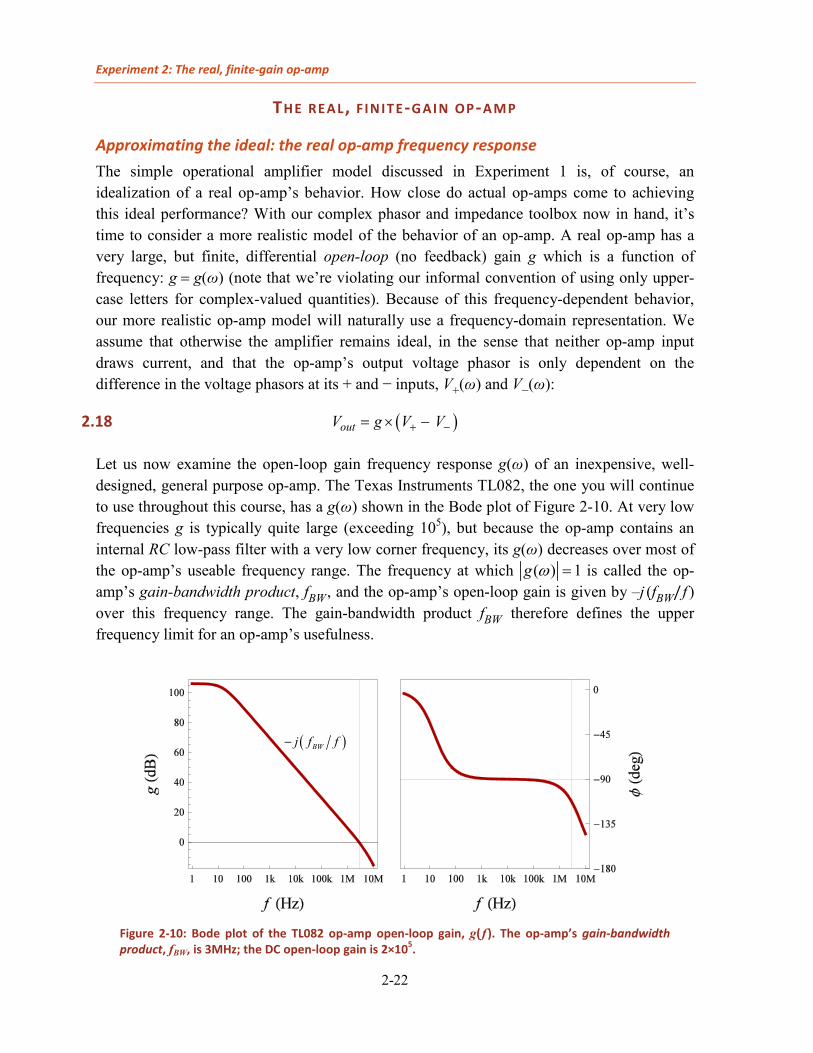
THE REAL, F INIT E-GAIN OP-AMP
Approximating the ideal: the real op-amp frequency response The simple operational amplifier model discussed in Experiment 1 is, of course, an idealization of a real op-amp’s behavior. How close do actual op-amps come to achieving this ideal performance? With our complex phasor and impedance toolbox now in hand, it’s time to consider a more realistic model of the behavior of an op-amp. A real op-amp has a very large, but finite, differential open-loop (no feedback) gain g which is a function of frequency: g = g(ω) (note that we’re violating our informal convention of using only upper-case letters for complex-valued quantities). Because of this frequency-dependent behavior, our more realistic op-amp model will naturally use a frequency-domain representation. We assume that otherwise the amplifier remains ideal, in the sense that neither op-amp input draws current, and that the op-amp’s output voltage phasor is only dependent on the difference in the voltage phasors at its + and − inputs, V+(ω) and V−(ω):
2.18 ( )outV g V V+ −= × −
Let us now examine the open-loop gain frequency response g(ω) of an inexpensive, well-designed, general purpose op-amp. The Texas Instruments TL082, the one you will continue to use throughout this course, has a g(ω) shown in the Bode plot of Figure 2-10. At very low frequencies g is typically quite large (exceeding 105), but because the op-amp contains an internal RC low-pass filter with a very low corner frequency, its g(ω) decreases over most of the op-amp’s useable frequency range. The frequency at which ( ) 1g ω = is called the op-amp’s gain-bandwidth product, fBW , and the op-amp’s open-loop gain is given by –j (fBW/f ) over this frequency range. The gain-bandwidth product fBW therefore defines the upper frequency limit for an op-amp’s usefulness.
Figure 2-10: Bode plot of the TL082 op-amp open-loop gain, g(f ). The op-amp’s gain-bandwidth product, fBW, is 3MHz; the DC open-loop gain is 2×10⁵.
( )BWj f f−

Introductory Electronics Laboratory
2-23
The roll-off in g(ω) shown in Figure 2-10 is an intentional design choice. It keeps the op-amp from exhibiting high frequency instability or oscillations, even when it is configured as a voltage follower circuit (with 100% feedback of Vout to V−). This sort of open-loop frequency response is known as unity-gain compensation, and it is what you will want for the vast majority of op-amp applications. A simple but useful 2-parameter model of the open-loop gain of an op-amp such as the TL082 is given in (2.19). The two parameters are gDC, the op-amp’s very large low frequency gain, and its gain-bandwidth product (or sometimes called its unity-gain bandwidth), fBW.
Simple op-amp open-loop gain model
2.19 1 1( ) BWDC
fjg f g f
= +
These two parameter values may be found in the op-amp device’s data sheet ; for a typical TL082 gDC = 2 ×10 5 and fBW = 3 MHz. 3 Note that this model is expressed in terms of conventional frequency f, not angular frequency ω. However, since only a frequency ratio is used, replacing the f ’s with ω’s in (2.19) won’t change the model. Using angular frequencies, the typical TL082 ωBW = 2 ×10 7 rad/sec.
Frequency responses of real amplifier circuits Now we examine the effect of a real op-amp’s finite open-loop gain function g(ω) on an amplifier circuit’s performance. The two typical op-amp circuit configurations, as we investigated in Experiment 1, are the noninverting and inverting amplifier circuits. Consider the ideal op-amp results first, whose gain formulas were derived in Experiment 1. Figure
3 The TL082 data sheet: http://www.sophphx.caltech.edu/Physics_5/Data_sheets/tl082.pdf .
Figure 2-11: Generic noninverting (left) and inverting (right) amplifier configurations. If the op-amps are ideal, then the voltage phasor relationships and resulting closed-loop amplifier gains will be as shown: GN for the ideal noninverting amplifier and –GI for the ideal inverting amplifier.
inV V+=
out NV V G− =
fZ
iZ
(ideal)
1 ( )ifNG Z Z= +
out inNV G V=
0V+ =
fZiZ
0V V− += =
inV
(ideal)
1ifI NG Z Z G= = −
out inIV G V= −

Experiment 2: The real, finite-gain op-amp
2-24
2-11 shows the circuits and their closed-loop (using feedback) gain expressions. These circuits assume that the feedback networks could contain arbitrary impedances Zf (ω) and Zi(ω) rather than the pure resistances used in Experiment 1. Thus we work in the frequency domain: the voltages are complex phasors and the gains are complex functions of ω. Recall that these circuits employ negative feedback via the voltage divider formed from Zf and Zi to return a fraction of Vout to the op-amp’s −Input terminal. The noninverting circuit’s resulting gain will be the reciprocal of that feedback fraction. As shown in the figure, we designate the noninverting ideal circuit gain as GN (ω). The ideal inverting circuit gain is the negative of the feedback impedances’ ratio and will be designated −GI (ω). Note that we do not include the inverting amplifier gain’s minus sign in our definition here of GI but will rather include it explicitly in our expressions.
How then will the gain formulas shown in Figure 2-11 change when the ideal op-amp is replaced with an op-amp with open-loop gain g(ω)? Consider the noninverting configuration first (left-hand circuit in Figure 2-11). Vout will now be given by the formula (2.18):
( )( )outV g V Vω + −= × − . V+ will still equal the input voltage Vin , and V− will still be the fraction of Vout determined by the Zf and Zi voltage divider: V− = Vout /GN . Putting all of this together,
( )
( )( )
1 ( )N N
N N N
out out outin in
out out in
V g V V G gV V g G
V g G V G g G gV
= × − = −
+ = + =
2.20 1( )
1 ( ) ( )NN
out
in
V GV G g
ωω ω
= +
( )( ) 1
( )f
Ni
ZG
Zω
ωω
≡ +
Noninverting configuration closed-loop gain (with finite op-amp open-loop gain)
So the noninverting amplifier gain is modified by the factor in brackets in (2.20). At frequencies where | ( )| | ( )|,Ng Gω ω the amplifier circuit will behave very close to ideal with gain very nearly equal to GN (ω). On the other hand, if | ( )| | ( )|,Ng Gω ω the circuit gain will approach the op-amp’s open loop gain g(ω), and the feedback network will have little effect.
What can happen at frequencies where | ( )| | ( )|Ng Gω ω≈ ? Now the circuit’s behavior will be strongly dependent on the phase of GN (ω)/g(ω), especially if that phase nears 180°! Since over most of the op-amp’s useful frequency range g(ω) will have a phase close to −90° (see Figure 2-10), problems will arise if the circuit design results in | ( )| | ( )|Ng Gω ω≈ and GN (ω) has a phase near +90°. In this case GN (ω)/g(ω) will approach −1, so the denominator of (2.20) becomes very small, resulting in usually undesirable behavior called gain peaking.
Most often, however, a simple op-amp amplifier design with two resistors for Zf and Zi will be required, such as in our old friend the ×11 noninverting amplifier with Rf = 10 Ri . In this
Introductory Electronics Laboratory
2-25
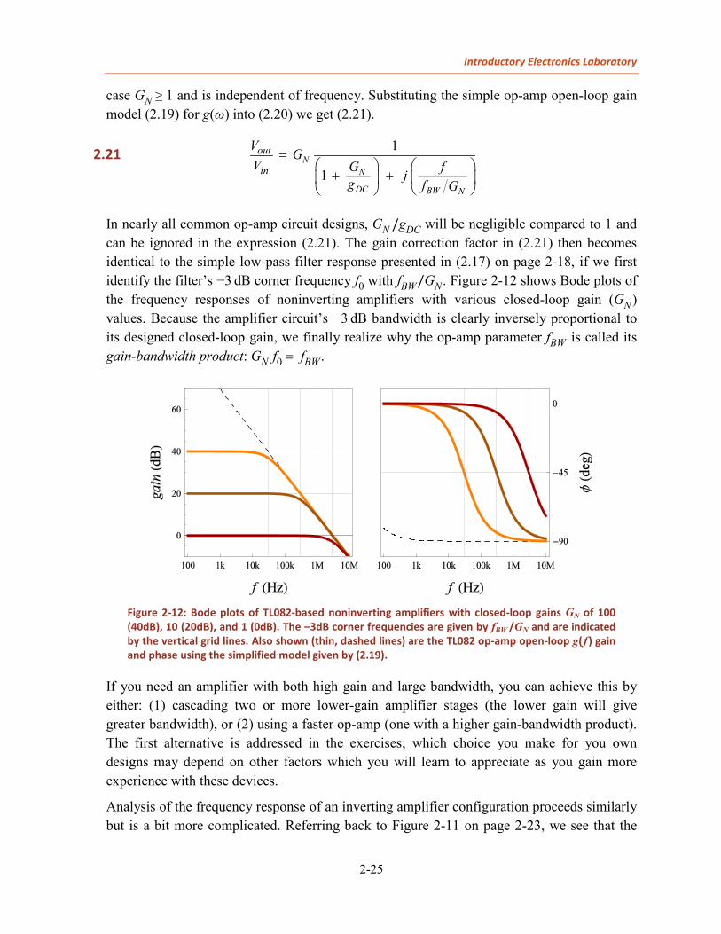
case GN ≥ 1 and is independent of frequency. Substituting the simple op-amp open-loop gain model (2.19) for g(ω) into (2.20) we get (2.21).
2.21 1
1N
N
DC BW N
out
in
V GV G fjg f G
=
+ +
In nearly all common op-amp circuit designs, GN /gDC will be negligible compared to 1 and can be ignored in the expression (2.21). The gain correction factor in (2.21) then becomes identical to the simple low-pass filter response presented in (2.17) on page 2-18, if we first identify the filter’s −3 dB corner frequency f0 with fBW/GN . Figure 2-12 shows Bode plots of the frequency responses of noninverting amplifiers with various closed-loop gain (GN) values. Because the amplifier circuit’s −3 dB bandwidth is clearly inversely proportional to its designed closed-loop gain, we finally realize why the op-amp parameter fBW is called its gain-bandwidth product: GN f0 = fBW .
Figure 2-12: Bode plots of TL082-based noninverting amplifiers with closed-loop gains GN of 100 (40dB), 10 (20dB), and 1 (0dB). The –3dB corner frequencies are given by fBW /GN and are indicated by the vertical grid lines. Also shown (thin, dashed lines) are the TL082 op-amp open-loop g(f ) gain and phase using the simplified model given by (2.19).
If you need an amplifier with both high gain and large bandwidth, you can achieve this by either: (1) cascading two or more lower-gain amplifier stages (the lower gain will give greater bandwidth), or (2) using a faster op-amp (one with a higher gain-bandwidth product). The first alternative is addressed in the exercises; which choice you make for you own designs may depend on other factors which you will learn to appreciate as you gain more experience with these devices.
Analysis of the frequency response of an inverting amplifier configuration proceeds similarly but is a bit more complicated. Referring back to Figure 2-11 on page 2-23, we see that the

Experiment 2: The real, finite-gain op-amp
2-26
op-amp gain equation (2.18) implies that .outgV V−− = We then use the generalized voltage divider equation from Experiment 1 to express V− in terms of contributions from Vin and Vout via the feedback impedances Zf (ω) and Zi(ω).
Equating the two expressions and solving for the circuit gain Vout / Vin gives:
( ) ( )
( ) ( )1 1
( ) 1
i f i f
f i f i I N N
out outin
out out outin in
V V g V Z V Z Z Z
V g V Z Z V Z Z G V G V G
− = − = + +
− = + + = +
2.22 1( )
1 ( ) ( )IN
out
in
V GV G g
ωω ω
= − +
( )( ) ; ( ) ( ) 1
( )f
I N Ii
ZG G G
Zω
ω ω ωω
≡ = +
Inverting configuration closed-loop gain (with finite op-amp open-loop gain)
So as expected, the ideal gain of the inverting amplifier circuit is reduced because of the op-amp’s finite gain. Note that the gain correction factor in (2.22) is identical to that found for the noninverting amplifier, (2.20): even though we use the inverting configuration with ideal gain −GI (ω), the inverting amplifier’s frequency response is determined by the feedback network’s equivalent noninverting gain, GN (ω) = GI (ω) + 1. This means, for example, that an inverting amplifier configuration with gain −1 has the same −3 dB bandwidth as a noninverting amplifier with a gain of 2: only half the op-amp’s unity-gain bandwidth, fBW . This behavior can be understood by looking at the circuits from the op-amp’s point of view: for either the noninverting or inverting configurations the negative feedback of Vout to its −Input is via a voltage divider formed from the same Zf and Zi — the only difference between the two circuits being where the designer chooses to introduce the input signal.
Introductory Electronics Laboratory
2-27
SKET CHING BODE PLOT S OF S IMPLE CIRCUIT S
Now we describe a few techniques to quickly sketch rough Bode plots of magnitude and phase for some simple circuit configurations. Although they won’t work for every circuit configuration, these technique remains broadly applicable and will help you start to develop your intuition regarding the behaviors of circuits and your skills at circuit design.
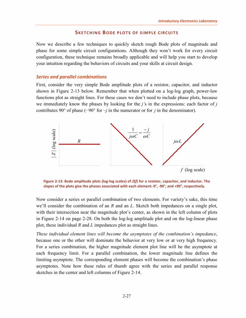
Series and parallel combinations First, consider the very simple Bode amplitude plots of a resistor, capacitor, and inductor shown in Figure 2-13 below. Remember that when plotted on a log-log graph, power-law functions plot as straight lines. For these cases we don’t need to include phase plots, because we immediately know the phases by looking for the j’s in the expressions: each factor of j contributes 90° of phase (−90° for –j in the numerator or for j in the denominator).
Figure 2-13: Bode amplitude plots (log-log scales) of Z(f) for a resistor, capacitor, and inductor. The slopes of the plots give the phases associated with each element: 0°, -90°, and +90°, respectively.
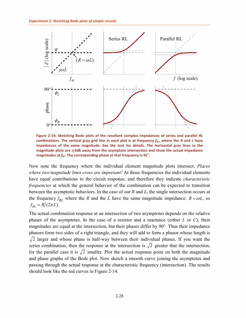
Now consider a series or parallel combination of two elements. For variety’s sake, this time we’ll consider the combination of an R and an L. Sketch both impedances on a single plot, with their intersection near the magnitude plot’s center, as shown in the left column of plots in Figure 2-14 on page 2-28. On both the log-log amplitude plot and on the log-linear phase plot, these individual R and L impedances plot as straight lines.
These individual element lines will become the asymptotes of the combination’s impedance, because one or the other will dominate the behavior at very low or at very high frequency. For a series combination, the higher magnitude element plot line will be the asymptote at each frequency limit. For a parallel combination, the lower magnitude line defines the limiting asymptote. The corresponding element phases will become the combination’s phase asymptotes. Note how these rules of thumb agree with the series and parallel response sketches in the center and left columns of Figure 2-14.
1 jj C Cω ω
−=
R
(log scale)f
|Z |(
log
scal
e)
j Lω
Experiment 2: Sketching Bode plots of simple circuits
2-28
Now note the frequency where the individual element magnitude plots intersect. Places where two magnitude lines cross are important! At those frequencies the individual elements have equal contributions to the circuit response, and therefore they indicate characteristic frequencies at which the general behavior of the combination can be expected to transition between the asymptotic behaviors. In the case of our R and L, the single intersection occurs at the frequency fRL where the R and the L have the same magnitude impedance: ,R Lω= so
(2 ).RLf R Lπ=
The actual combination response at an intersection of two asymptotes depends on the relative phases of the asymptotes. In the case of a resistor and a reactance (either L or C), their magnitudes are equal at the intersection, but their phases differ by 90°. Thus their impedance phasors form two sides of a right triangle, and they will add to form a phasor whose length is
2 larger and whose phase is half-way between their individual phases. If you want the series combination, then the response at the intersection is 2 greater that the intersection; for the parallel case it is 2 smaller. Plot the actual response point on both the magnitude and phase graphs of the Bode plot. Now sketch a smooth curve joining the asymptotes and passing through the actual response at the characteristic frequency (intersection). The results should look like the red curves in Figure 2-14.
Figure 2-14: Sketching Bode plots of the resultant complex impedances of series and parallel RL combinations. The vertical gray grid line in each plot is at frequency fRL, where the R and L have impedances of the same magnitude. See the text for details. The horizontal gray lines in the magnitude plots are ±3dB away from the asymptote intersection and show the actual impedance magnitudes at fRL. The corresponding phase at that frequency is 45°.
|Z |(
log
scal
e)
(log scale)f
j Lω
R
Series RL Parallel RL
phas
e
0°
90°
RLf
( )R Lω=
Rφ
Lφ
Introductory Electronics Laboratory
2-29
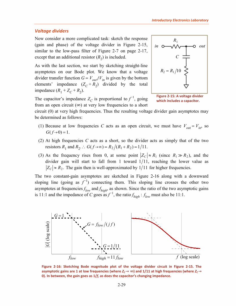
Voltage dividers Now consider a more complicated task: sketch the response (gain and phase) of the voltage divider in Figure 2-15, similar to the low-pass filter of Figure 2-7 on page 2-17, except that an additional resistor (R2) is included.
As with the last section, we start by sketching straight-line asymptotes on our Bode plot. We know that a voltage divider transfer function G = Vout/Vin is given by the bottom elements’ impedance (ZC + R2) divided by the total impedance (R1 + ZC + R2).
The capacitor’s impedance ZC is proportional to f −1, going from an open circuit (∞) at very low frequencies to a short circuit (0) at very high frequencies. Thus the resulting voltage divider gain asymptotes may be determined as follows:
(1) Because at low frequencies C acts as an open circuit, we must have Vout = Vin, so ( 0) 1.G f → =
(2) At high frequencies C acts as a short, so the divider acts as simply that of the two resistors R1 and R2. 2 1 2( ) ( ) 1 11.G f R R R→∴ ∞ = + =
(3) As the frequency rises from 0, at some point 1CZ R≈ (since 1 2 ),R R and the divider gain will start to fall from 1 toward 1 11, reaching the lower value as
2.CZ R≈ The gain then is well-approximated by 1 11 for higher frequencies.
The two constant-gain asymptotes are sketched in Figure 2-16 along with a downward sloping line (going as f −1) connecting them. This sloping line crosses the other two asymptotes at frequencies flow and fhigh, as shown. Since the ratio of the two asymptotic gains is 11:1 and the impedance of C goes as f −1, the ratio fhigh : flow must also be 11:1.
Figure 2-15: A voltage divider which includes a capacitor.
Figure 2-16: Sketching Bode magnitude plot of the voltage divider circuit in Figure 2-15. The asymptotic gains are 1 at low frequencies (where ZC → ∞) and 1/11 at high frequencies (where ZC → 0). In between, the gain goes as 1/f, as does the capacitor’s changing impedance.
R1
C
in out
2 1 10R R=
|G|(
log
scal
e)
1G =
1 11G =
( )lowG f j f=
lowf 11high lowf f= (log scale)f

Experiment 2: Sketching Bode plots of simple circuits
2-30
Before determining flow and fhigh , which we know should be approximately given by 11 (2 )R Cπ and 21 (2 ) ,R Cπ respectively, consider the phase response. Using the advice
given in the highlighted box way back on page 2-19, we know that the asymptotic phase is 0° where the gain is independent of frequency and is −90° where the gain ∝ f −1 (note the gain expression in Figure 2-16).
Figure 2-17: Sketching Bode phase plot of the voltage divider circuit in Figure 2-15. The asymptotic phase is 0 where the asymptotic gain is constant and is −90° where the gain goes as 1/( j f ). It turns out that the actual phase changes so slowly, however, that it doesn’t nearly reach the −90° asymptote (right plot).
The phase asymptotes are sketched in Figure 2-17 along with the complex gain formulas associated with each. In this example the two frequencies marking the asymptotic phase shifts are only about an order of magnitude apart, and the phase actually changes quite slowly for these sorts of simple filters. Keep this fact in mind when sketching the phase. The actual phase response is plotted in the right-hand graph of Figure 2-17; the phase goes down to only about −56°. You can also see that it doesn’t approach 0° unless the frequency is well away from both flow and fhigh .
The final requirement is to determine flow and fhigh . The original estimates are 1CZ R≈ at flow and 2CZ R≈ at fhigh , and these estimates are perfectly adequate in many situations, so that we can then estimate 1
1(2 ) ,lowf R Cπ −= 21(2 ) .highf R Cπ −=
However, because the gain change is by a factor of 11, we know that the ratio fhigh : flow must also be 11:1. So which frequency estimate is wrong: flow , fhigh , or both? It turns out that flow =
1 21[ 2 ( ) ] ,R R Cπ −+ a factor of 11 smaller than 2
1(2 ) .highf R Cπ −= You can see that this should be the case by looking again at the circuit schematic in Figure 2-15. If the input is 0, then the input end of R1 is connected to the grounded end of R2. From the point of view of the capacitor C, it would discharge through the two series-connected resistors, and the relevant RC time constant would be (R1 + R2) C, determining flow . The other time constant, corresponding to fhigh , would then be 1/11 of this, or R2C (for R1 = 10R2). Such level of detail is not required when you are simply trying to sketch the Bode plots.
1G = 1 11G =
( )lowG f j f=
lowf 11high lowf f= (log)fphas
e
0°
−90°
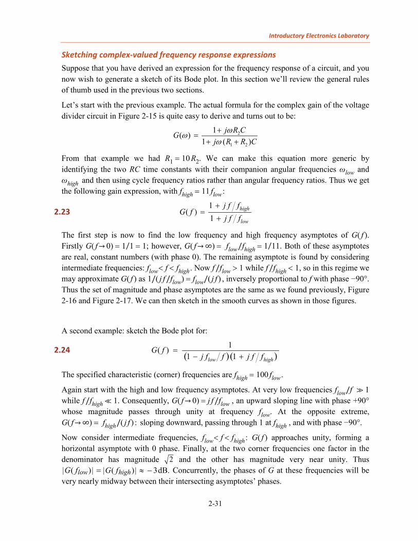
Introductory Electronics Laboratory
2-31
Sketching complex-valued frequency response expressions Suppose that you have derived an expression for the frequency response of a circuit, and you now wish to generate a sketch of its Bode plot. In this section we’ll review the general rules of thumb used in the previous two sections.
Let’s start with the previous example. The actual formula for the complex gain of the voltage divider circuit in Figure 2-15 is quite easy to derive and turns out to be:
2
1 2
1( )1 ( )
j R CGj R R C
ωωω+
=+ +
From that example we had R1 = 10 R2. We can make this equation more generic by identifying the two RC time constants with their companion angular frequencies ωlow and ωhigh and then using cycle frequency ratios rather than angular frequency ratios. Thus we get the following gain expression, with fhigh = 11 flow:
2.23 1
( )1
high
low
j f fG f
j f f+
=+
The first step is now to find the low frequency and high frequency asymptotes of G( f ). Firstly G( f→ 0) = 1/1 = 1; however, G( f→∞) = flow/fhigh = 1/11. Both of these asymptotes are real, constant numbers (with phase 0). The remaining asymptote is found by considering intermediate frequencies: flow< f < fhigh . Now f /flow > 1 while f /fhigh < 1, so in this regime we may approximate G( f ) as 1/( j f /flow) = flow/( j f ) , inversely proportional to f with phase −90°. Thus the set of magnitude and phase asymptotes are the same as we found previously, Figure 2-16 and Figure 2-17. We can then sketch in the smooth curves as shown in those figures.
A second example: sketch the Bode plot for:
2.24 1( )1 1( )( )low high
G fj f f j f f
=− +
The specified characteristic (corner) frequencies are fhigh = 100 flow .
Again start with the high and low frequency asymptotes. At very low frequencies flow/f 1 while f /fhigh 1. Consequently, G( f→ 0) = j f /flow , an upward sloping line with phase +90° whose magnitude passes through unity at frequency flow. At the opposite extreme, G( f→∞) = fhigh/( j f ) : sloping downward, passing through 1 at fhigh , and with phase −90°.
Now consider intermediate frequencies, flow< f < fhigh : G( f ) approaches unity, forming a horizontal asymptote with 0 phase. Finally, at the two corner frequencies one factor in the denominator has magnitude 2 and the other has magnitude very near unity. Thus | ( )|lowG f = | ( )| 3dB.highG f ≈ − Concurrently, the phases of G at these frequencies will be very nearly midway between their intersecting asymptotes’ phases.

Experiment 2: Sketching Bode plots of simple circuits
2-32
The resulting Bode plot sketch is shown below. As you can see, the response is that of a band-pass filter. The response expression (2.24) is the product of a low-pass and a high-pass filter response, (2.17), with corner frequencies a factor of 100 apart.
Figure 2-18: Sketching the Bode plot of the bandpass filter whose complex gain is given by (2.24). The two corner frequencies have a ratio of 100:1. The phase plot (right) covers a larger frequency range than does the magnitude plot (left).
More practice sketching Bode plots is left to the Prelab exercises.

Introductory Electronics Laboratory
2-33
THE T RANSIENT RESPONSE OF A S IMPLE F ILT ER
So far we have investigated the frequency responses of a variety of simple filters. Such frequency-domain, phasor expressions describe the amplitude gain and phase shift of a filter’s sinusoidal output relative to that of a continuous, sinusoidal signal applied at its input (as a function of the signal input frequency). What we now address is how this phasor relationship G( f ) corresponds to the filter’s response to a sudden, nearly discontinuous change in its input. This will be a time-domain analysis of the filter output vout(t) in response to its input vin(t). In particular, we wish to understand how such a filter will respond to a square-wave input signal: the input voltage repeatedly switches suddenly between two values: ±V. Between shifts the input voltage is held constant long enough to observe the filter output’s behavior as it settles to equilibrium. This output behavior is called the filter’s transient response, and the time it takes for the filter output to converge to within some small range about its equilibrium value is called its settling time.
We first looked at an example of a transient response analysis when we investigated the exponential relaxation of the voltage across a capacitor in the section The RC time constant starting on page 2-3. We now expand on that presentation to include more general circuit descriptions, starting with the simple RC high-pass and low-pass filters we’ve already discussed. As we stressed when we introduced the concept of impedance, complex-valued, algebraic, frequency-domain descriptions of a circuit correspond to differential time-domain expressions, the fundamental connection between these representations being (2.8), summarized as:
2.25 ( ) ( )dj F f tdt
ω ω ↔
where F(ω) and f (t) are corresponding frequency-domain and time-domain representations of the same underlying function. In other words, we identify multiplication by jω with a time derivative d /dt. Let’s apply this idea to the high-pass and low-pass filter responses of (2.17) on page 2-18. To properly use the mapping (2.25), however, our frequency-domain expressions must use angular frequencies and not cyclic frequencies (rad/sec, not Hz). Applying this procedure to the filter frequency-domain responses:
High-pass filter response Low-pass filter response
0
0
( )1( )1 ( )
( ) ( ) ( )
HPout
in
out in
VG
j V
j V j V
ωω
ω ω ω
ω ω ω ω ω
= =+
+ =
0
0 0
( )1( )1 ( )
( ) ( ) ( )
LPout
in
out in
VG
j V
j V V
ωω
ω ω ω
ω ω ω ω ω
= =+
+ =
2.26 0( ) ( ) ( )out out ind dv t v t v tdt dtω+ = 0 0( ) ( ) ( )out out in
d v t v t v tdt ω ω+ =
These are the time-domain, differential equations relating vout(t) and vin(t). Both have the same homogeneous differential equation for their complementary solution (set the right-hand
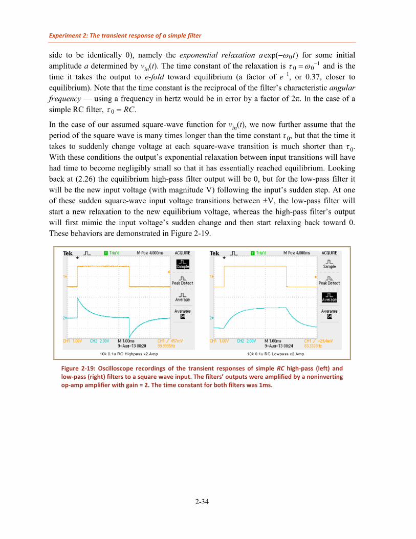
Experiment 2: The transient response of a simple filter
2-34
side to be identically 0), namely the exponential relaxation 0exp( )a tω− for some initial amplitude a determined by vin(t). The time constant of the relaxation is 1
0 0t ω −= and is the time it takes the output to e-fold toward equilibrium (a factor of e−1, or 0.37, closer to equilibrium). Note that the time constant is the reciprocal of the filter’s characteristic angular frequency — using a frequency in hertz would be in error by a factor of 2π. In the case of a simple RC filter, 0 .RCt =
In the case of our assumed square-wave function for vin(t), we now further assume that the period of the square wave is many times longer than the time constant τ 0, but that the time it takes to suddenly change voltage at each square-wave transition is much shorter than τ 0. With these conditions the output’s exponential relaxation between input transitions will have had time to become negligibly small so that it has essentially reached equilibrium. Looking back at (2.26) the equilibrium high-pass filter output will be 0, but for the low-pass filter it will be the new input voltage (with magnitude V) following the input’s sudden step. At one of these sudden square-wave input voltage transitions between ±V, the low-pass filter will start a new relaxation to the new equilibrium voltage, whereas the high-pass filter’s output will first mimic the input voltage’s sudden change and then start relaxing back toward 0. These behaviors are demonstrated in Figure 2-19.
Figure 2-19: Oscilloscope recordings of the transient responses of simple RC high-pass (left) and low-pass (right) filters to a square wave input. The filters’ outputs were amplified by a noninverting op-amp amplifier with gain = 2. The time constant for both filters was 1ms.
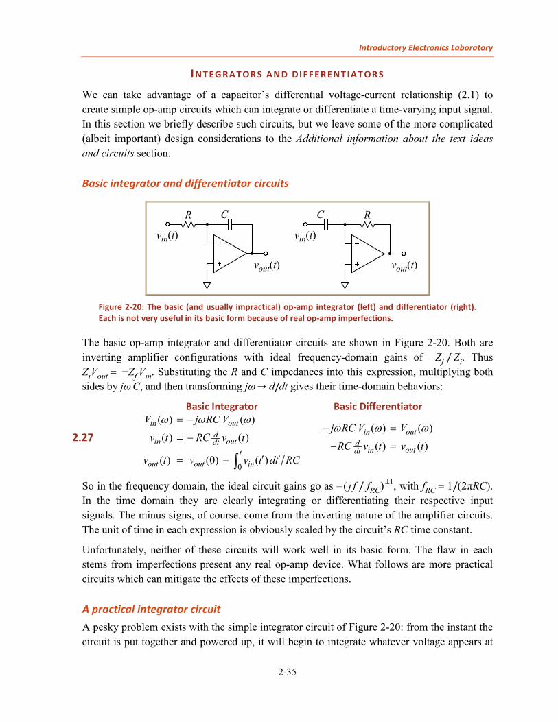
Introductory Electronics Laboratory
2-35
INT EGRAT ORS AND DIFFERENT IAT ORS
We can take advantage of a capacitor’s differential voltage-current relationship (2.1) to create simple op-amp circuits which can integrate or differentiate a time-varying input signal. In this section we briefly describe such circuits, but we leave some of the more complicated (albeit important) design considerations to the Additional information about the text ideas and circuits section.
Basic integrator and differentiator circuits
Figure 2-20: The basic (and usually impractical) op-amp integrator (left) and differentiator (right). Each is not very useful in its basic form because of real op-amp imperfections.
The basic op-amp integrator and differentiator circuits are shown in Figure 2-20. Both are inverting amplifier configurations with ideal frequency-domain gains of −Zf / Zi. Thus ZiVout = −Zf Vin. Substituting the R and C impedances into this expression, multiplying both sides by jωC, and then transforming jω→ d/dt gives their time-domain behaviors:
Basic Integrator Basic Differentiator
2.27
0
( ) ( )
( ) ( )
( ) (0) ( )
outind
outin dtt
out out in
V j RC Vv t RC v t
v t v v t dt RC
ω ω ω= −
= −
′ ′= − ∫
( ) ( )
( ) ( )outin
doutindt
j RC V VRC v t v t
ω ω ω− =
− =
So in the frequency domain, the ideal circuit gains go as – ( j f / fRC) ±1, with fRC = 1/(2πRC). In the time domain they are clearly integrating or differentiating their respective input signals. The minus signs, of course, come from the inverting nature of the amplifier circuits. The unit of time in each expression is obviously scaled by the circuit’s RC time constant.
Unfortunately, neither of these circuits will work well in its basic form. The flaw in each stems from imperfections present any real op-amp device. What follows are more practical circuits which can mitigate the effects of these imperfections.
A practical integrator circuit A pesky problem exists with the simple integrator circuit of Figure 2-20: from the instant the circuit is put together and powered up, it will begin to integrate whatever voltage appears at
vin(t)
vout(t)
R C
vin(t)
vout(t)
RC
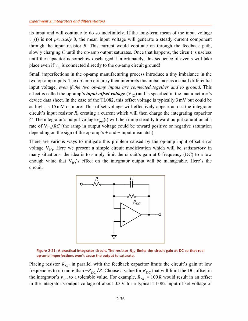
Experiment 2: Integrators and differentiators
2-36
its input and will continue to do so indefinitely. If the long-term mean of the input voltage vin(t) is not precisely 0, the mean input voltage will generate a steady current component through the input resistor R. This current would continue on through the feedback path, slowly charging C until the op-amp output saturates. Once that happens, the circuit is useless until the capacitor is somehow discharged. Unfortunately, this sequence of events will take place even if vin is connected directly to the op-amp circuit ground!
Small imperfections in the op-amp manufacturing process introduce a tiny imbalance in the two op-amp inputs. The op-amp circuitry then interprets this imbalance as a small differential input voltage, even if the two op-amp inputs are connected together and to ground. This effect is called the op-amp’s input offset voltage (VIO) and is specified in the manufacturer’s device data sheet. In the case of the TL082, this offset voltage is typically 3 mV but could be as high as 15 mV or more. This offset voltage will effectively appear across the integrator circuit’s input resistor R, creating a current which will then charge the integrating capacitor C. The integrator’s output voltage vout(t) will then ramp steadily toward output saturation at a rate of VIO/RC (the ramp in output voltage could be toward positive or negative saturation depending on the sign of the op-amp’s + and − input mismatch).
There are various ways to mitigate this problem caused by the op-amp input offset error voltage VIO. Here we present a simple circuit modification which will be satisfactory in many situations: the idea is to simply limit the circuit’s gain at 0 frequency (DC) to a low enough value that VIO’s effect on the integrator output will be manageable. Here’s the circuit:
Figure 2-21: A practical integrator circuit. The resistor RDC limits the circuit gain at DC so that real op-amp imperfections won’t cause the output to saturate.
Placing resistor RDC in parallel with the feedback capacitor limits the circuit’s gain at low frequencies to no more than −RDC/R. Choose a value for RDC that will limit the DC offset in the integrator’s vout to a tolerable value. For example, RDC = 100 R would result in an offset in the integrator’s output voltage of about 0.3 V for a typical TL082 input offset voltage of
R C
DCR
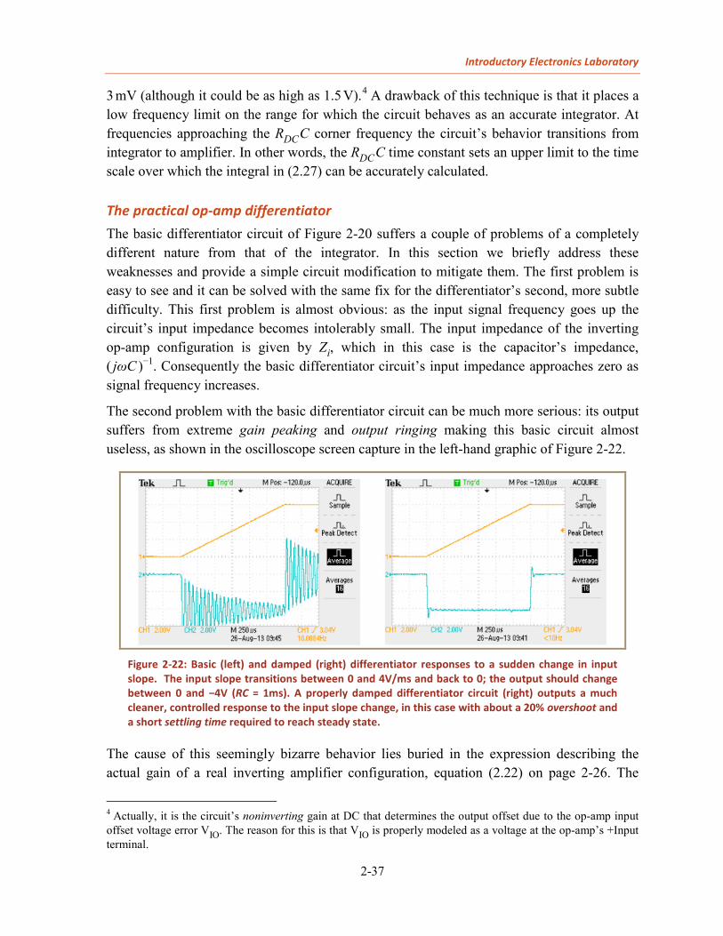
Introductory Electronics Laboratory
2-37
3 mV (although it could be as high as 1.5 V).4 A drawback of this technique is that it places a low frequency limit on the range for which the circuit behaves as an accurate integrator. At frequencies approaching the RDCC corner frequency the circuit’s behavior transitions from integrator to amplifier. In other words, the RDCC time constant sets an upper limit to the time scale over which the integral in (2.27) can be accurately calculated.
The practical op-amp differentiator The basic differentiator circuit of Figure 2-20 suffers a couple of problems of a completely different nature from that of the integrator. In this section we briefly address these weaknesses and provide a simple circuit modification to mitigate them. The first problem is easy to see and it can be solved with the same fix for the differentiator’s second, more subtle difficulty. This first problem is almost obvious: as the input signal frequency goes up the circuit’s input impedance becomes intolerably small. The input impedance of the inverting op-amp configuration is given by Zi, which in this case is the capacitor’s impedance, ( jωC )−1. Consequently the basic differentiator circuit’s input impedance approaches zero as signal frequency increases.
The second problem with the basic differentiator circuit can be much more serious: its output suffers from extreme gain peaking and output ringing making this basic circuit almost useless, as shown in the oscilloscope screen capture in the left-hand graphic of Figure 2-22.
Figure 2-22: Basic (left) and damped (right) differentiator responses to a sudden change in input slope. The input slope transitions between 0 and 4V/ms and back to 0; the output should change between 0 and −4V (RC = 1ms). A properly damped differentiator circuit (right) outputs a much cleaner, controlled response to the input slope change, in this case with about a 20% overshoot and a short settling time required to reach steady state.
The cause of this seemingly bizarre behavior lies buried in the expression describing the actual gain of a real inverting amplifier configuration, equation (2.22) on page 2-26. The
4 Actually, it is the circuit’s noninverting gain at DC that determines the output offset due to the op-amp input offset voltage error VIO. The reason for this is that VIO is properly modeled as a voltage at the op-amp’s +Input terminal.

Experiment 2: Integrators and differentiators
2-38
difficulty arises because of the interplay between the op-amp’s finite bandwidth (represented by its gain-bandwidth product, ωBW) and the differentiator circuit’s ideal gain function GI (ω) = jωRC ≡ jω/ωRC . Here’s why: remembering that the ideal noninverting gain is one more than the inverting gain, ( ) ( ) 1,N IG Gω ω= + equation (2.22) for our basic differentiator transfer function becomes:
1( ) 11 ( ) ( ) 1( ) ( )
RCI
RCN
out
in
jV G jV G gg g
ω ωω ω ωω ωω ω
− = = + + +
Dividing top and bottom by the numerator, substituting for g(ω), and gathering terms (where we’ve ignored imaginary-part terms of order 1/gDC),
2.28 11RC RC
BW BWDC
out
in
VV
jgω ωω ω
ωω
− =
+ + −
As expected, the op-amp’s falling open-loop gain takes over the circuit’s response at high frequency, limiting the range over which the differentiator works to frequencies less than about ω0 = (ωRC ωBW)1/2, the frequency at which |GI (ω)| = |g(ω)|.
Assume that ωRC ωBW , as is normally the case: we’ll use the example of Figure 2-22, with ωRC = 103 sec−1 and the TL082’s ωBW = 2 × 10⁷ sec−1. Then ω0 = 1.4 × 10⁵ sec−1 ( f0 = 22 kHz), and we might expect the circuit’s gain at ω0 to be |GI (ω0)| = |g(ω0)| = ω0 /ωRC = 140. However, if we substitute ω = ω0 into (2.28) the imaginary part of the denominator vanishes, and (with gDC ≈ 10ωBW /ωRC) the gain is actually around 104, about 100 times higher than expected! This extreme gain peaking is an example of a high-Q, resonant response (which we will study in more detail during Experiment 5). It also explains the ringing (at the circuit resonant frequency f0) observed in the left-hand oscilloscope screen image in Figure 2-22.
Figure 2-23: A practical differentiator circuit. The resistor Rd damps the overshoot and ringing that would otherwise plague the differentiator’s output. It also provides a minimum input impedance for the circuit at high frequencies.
Rd C R
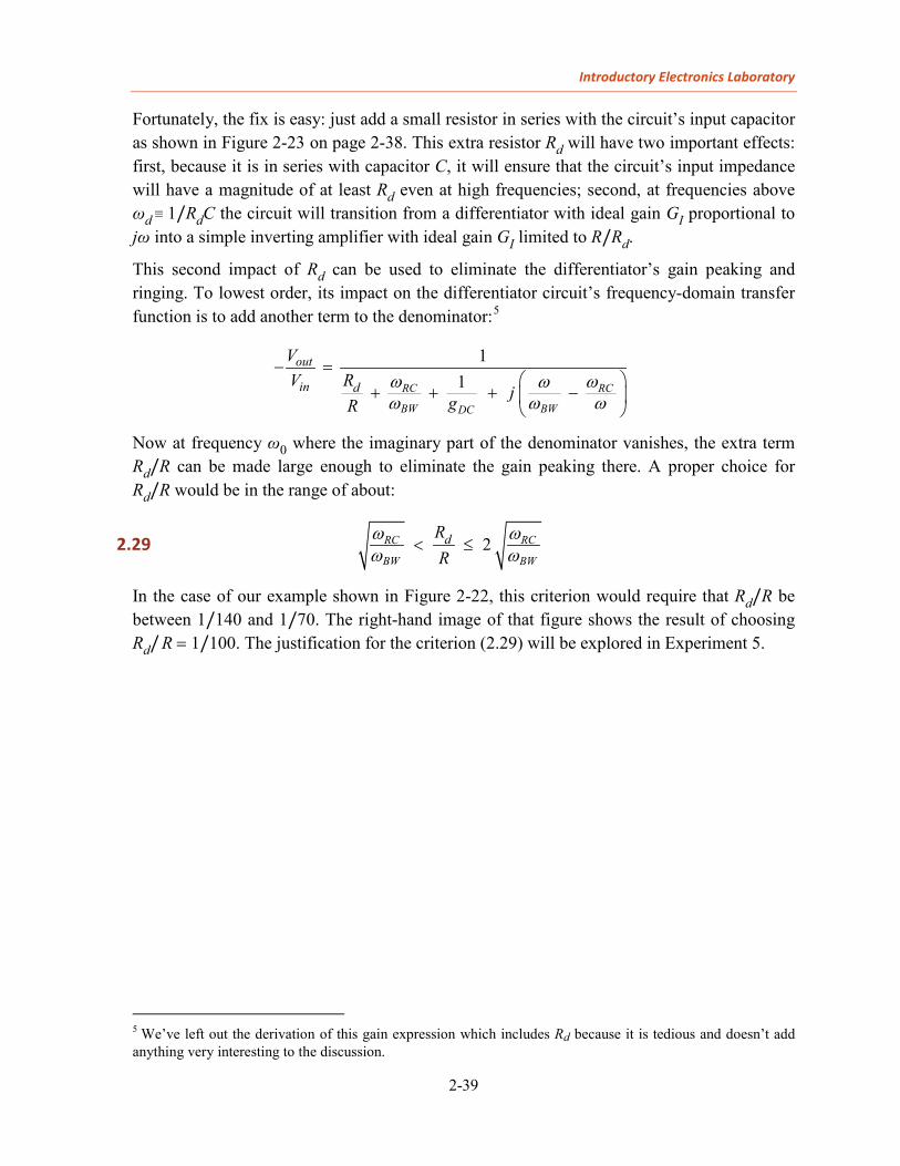
Introductory Electronics Laboratory
2-39
Fortunately, the fix is easy: just add a small resistor in series with the circuit’s input capacitor as shown in Figure 2-23 on page 2-38. This extra resistor Rd will have two important effects: first, because it is in series with capacitor C, it will ensure that the circuit’s input impedance will have a magnitude of at least Rd even at high frequencies; second, at frequencies above ωd ≡ 1/RdC the circuit will transition from a differentiator with ideal gain GI proportional to jω into a simple inverting amplifier with ideal gain GI limited to R/Rd.
This second impact of Rd can be used to eliminate the differentiator’s gain peaking and ringing. To lowest order, its impact on the differentiator circuit’s frequency-domain transfer function is to add another term to the denominator:5
11RC RC
BW BWDC
out
in dg
VRV
jR
ω ωω ω
ωω
− =
+ + + −
Now at frequency ω0 where the imaginary part of the denominator vanishes, the extra term Rd/R can be made large enough to eliminate the gain peaking there. A proper choice for Rd/R would be in the range of about:
2.29 2RC RC
BW BW
dRR
ω ωω ω< ≤
In the case of our example shown in Figure 2-22, this criterion would require that Rd/R be between 1/140 and 1/70. The right-hand image of that figure shows the result of choosing Rd/ R = 1/100. The justification for the criterion (2.29) will be explored in Experiment 5.
5 We’ve left out the derivation of this gain expression which includes Rd because it is tedious and doesn’t add anything very interesting to the discussion.
Experiment 2: Prelab exercises
2-40
PRELAB EXERCISES
1. Show that the total equivalent capacitance of two or more ideal capacitors connected in parallel is equal to the sum of their individual capacitance values.
2. Derive equations (2.17) for the RC high-pass and low-pass filter frequency responses, G(ω), from the equations just above them on page 2-18.
3. Consider the AC coupled amplifier in the example shown in Figure 2-9 on page 2-20. What should be the value of R if the amplifier circuit’s input impedance should be at least 100 kΩ within its passband? The audio frequency range is nominally taken to be 20 Hz–20 kHz. What should be the minimum value of C if you want no more than 3 dB attenuation (reduction in gain) of a signal in this frequency range?
4. You cascade two noninverting op-amp amplifier circuits, each with a gain of 11 (cascade: connect the output of one circuit to the input of another, as in circuit (b) above). What is the resulting gain of the combined amplifiers? If both amplifiers use the TL082 op-amp ( fBW = 3 MHz), what would be the −3 dB corner frequency for each amplifier stage? What will then be the gain of the cascaded amplifier combination at this frequency? Sketch a schematic of this circuit: label feedback resistors with appropriate choices for their values; label the input and output terminals.
5. Sketch Bode plots of the gain for the following filters, both magnitude and phase vs. frequency (input at left, output at right for each circuit). Use appropriate log scales for the plots and sketch the asymptotes (which should be straight lines). Calculate the corner frequencies (there are two for each circuit). Label each asymptote with its G( f ) function, including its phase (e.g. j for +90°, –j for −90°, etc., as in Figure 2-8). Messy algebra shouldn’t be required to complete this exercise.
(a)
(b)
Introductory Electronics Laboratory
2-41
LAB PROCEDURE During lab you will investigate the frequency responses (magnitude and phase) of various simple filters and op-amp circuits. You will add another tool to your bag of tricks, the lab’s Frequency Response program, which will take control of your lab signal generator and use the computer data acquisition system (DAQ) to generate Bode plots of the transfer functions of amplifiers and filters. In effect, this generator+DAQ system emulates the function of a Network Analyzer, a sophisticated laboratory instrument for measuring the transfer function and terminal impedances of a 2-port network as a function of frequency. The course instructor will give a quick demo of the Frequency Response program at the start of your lab session.
You can capture images of plots the Frequency Response program generates and print them directly from the program. You can also save transfer function data as a text file which can then be loaded back into the program or can be manipulated and plotted using other applications (including spreadsheet programs).
Gain-bandwidth product limitations of op-amp amplifiers Assemble a ×11 noninverting amplifier (as in Experiment 1). Use a pair of BNC cables to connect the amplifier circuit’s input and output to the two computer DAQ analog inputs (AI0 and AI1). Use a third BNC cable to connect the signal generator’s SYNC OUTPUT to the DAQ PFI0 input (this is a digital signal from the generator that will be used to trigger DAQ data acquisition events).
The computer DAQ system requires a digital signal synchronized with the circuit analog signals to trigger its data acquisitions. Without this digital signal, the computer will never acquire data.
Make sure everything is powered up and working, and then start the Frequency Response application. The program will momentarily take control of the signal generator and set its frequency to 1 kHz and set its amplitude to 100 mVpp. Next use the program’s Manual Control mode (select the program’s tab) and find the amplifier’s −3 dB bandwidth (gain drops to only 0.71×11, or about 8), which should be at frequency fBW/11. Do this task by manually adjusting the signal generator’s frequency controls as you watch the program’s gain and phase “thermometers.” Is the −3 dB frequency you find consistent with the TL082’s typical fBW of 3 MHz? What should be the phase shift of the amplifier’s transfer function at this frequency? Now use the program’s Sweep mode to measure and plot the amplifier’s frequency response from 1 kHz to 1 MHz (take about 80 data points and use log scales for the graph). Examine both the gain magnitude and the gain phase graphs.
Experiment 2: Lab procedure
2-42
Make sure to select the Save All radio button in the Frequency Response program’s data save dialog box. Otherwise, you won’t be able to reload the saved data set back into the program.
Save this response data so that you can reload it later.
Assemble another ×11 noninverting amplifier and cascade its input to the output of the first amplifier to give a 2-stage amplifier. Manually adjust the signal generator amplitude to limit the output of this second stage to no more than 5 or 6 volts. Again use the manual mode of the frequency response program and adjust the program’s ADC gains so that both input and response waveforms fit in their displays. Sweep the 2-stage amplifier’s frequency response and compare it to that for the single ×11 stage. Save this 2-stage amplifier frequency response data.
Now disconnect the second amplifier and modify the original amplifier circuit to construct a single-stage noninverting amplifier with a gain of about 121. Use a 1k resistor for Ri ; what should be the value for Rf ? Your lab instructor or TA will show you how to connect an odd resistor into the breadboard circuit. Sweep this amplifier’s frequency response from 1 kHz to 1 MHz and save the data.
How does its −3 dB bandwidth compare to what you would expect for a single-stage ×121 amplifier? How does it compare to your 2-stage amplifier’s bandwidth? Plot both frequency response curves on a single graph. Now compare the single-stage ×121 frequency response to that of the single-stage ×11 amplifier. Do the frequency responses align like those in Figure 2-12 on page 2-25?
Transient Response Now change the signal generator output to a square wave and set its frequency to about 4 kHz. Use the oscilloscope to examine the rising and falling edges of the output from your single-stage ×121 amplifier. Is the output response to each input step an exponential relaxation similar to the right-hand image of Figure 2-19? Using the oscilloscope cursor function, estimate the time constant τ 0 of one of these exponential relaxations. Does it agree with your amplifier’s −3 dB bandwidth (2π f0 = 1/τ 0)? Save a screen capture of your data.
Adding AC coupling to an amplifier input Staying with the single-stage ×121 noninverting amplifier you’ve built, notice that the trainer board also has a selection of preinstalled resistors and capacitors attached to the op-amp’s +Input. You can use a couple of these components to incorporate a simple RC high-pass filter at the noninverting circuit’s input (Figure 2-9). Use the op-amp +Input’s 10 kΩ resistor and select a capacitor which will give a corner frequency of about 160 Hz. Return the signal generator’s output to a sine wave and select the Manual Tab of the frequency response

Introductory Electronics Laboratory
2-43
program. Adjust the generator frequency to find the AC coupling (high-pass) filter’s corner frequency. What should be the amplifier output’s phase shift at this frequency? Adjust the signal generator to add a DC offset voltage to the input signal. Does the offset affect the amplifier output? Remember to reset the signal generator offset voltage to 0 when you’ve finished. Sweep the AC-coupled amplifier’s frequency response from 50 Hz to 100 kHz and compare it to your saved single-stage ×121 frequency response data.
Does the ×121 amplifier exhibit a constant DC output of a few tenths of a volt, even with the AC coupled input filter? The TL082 op-amps typically have an input offset voltage error (VIO) of around 3 mV. Could this explain the observed DC output voltage?
Additional, self-directed investigations If you have time, build a circuit from the MORE CIRCUIT IDEAS section or from some other section of the text. Investigate its frequency response as well as its transient behavior (response to a square-wave input).
Particularly interesting might be the op-amp integrator circuit, Figure 2-21 on page 2-36. If you attempt this one, assemble the circuit with 0.1 msecRC = . At what frequency do you expect 1G = ? Select a value for 100DCR R≈ ; your instructor or TA can show you how to wire it into the breadboard circuit. What should be the circuit’s DC gain? With the input grounded, do you see an output offset voltage error? Input a square wave at about 1kHz and about 0.5Vpp. Using the oscilloscope, compare the output and input waveforms. Is the relationship consistent with the integrator circuit’s differential equation in the second line of (2.27) on page 2-35? Watch the output on the oscilloscope as you disconnect one end of DCR from the circuit. About how long does it take for the output voltage to saturate?
In the unlikely event that you still have time remaining, look back at Experiment 1 to see if there are any other circuits from that chapter you would like to investigate.
Lab results write-up Include a sketch of the schematic with component values for each circuit you investigate, along with appropriate oscilloscope screen shots and Bode plots. Make sure you’ve answered each of the questions posed.
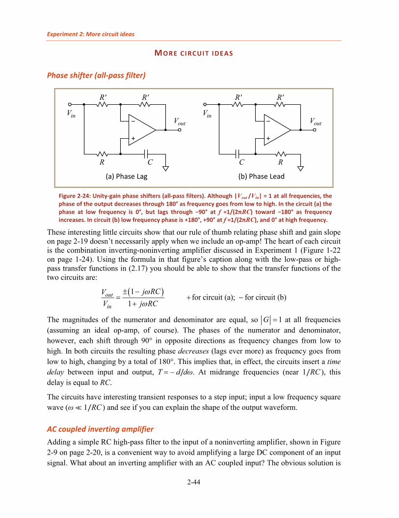
Experiment 2: More circuit ideas
2-44
MORE CIRCUIT IDEAS
Phase shifter (all-pass filter)
Figure 2-24: Unity-gain phase shifters (all-pass filters). Although |Vout /Vin| = 1 at all frequencies, the phase of the output decreases through 180° as frequency goes from low to high. In the circuit (a) the phase at low frequency is 0°, but lags through −90° at f =1/(2πRC) toward −180° as frequency increases. In circuit (b) low frequency phase is +180°, +90° at f =1/(2πRC), and 0° at high frequency.
These interesting little circuits show that our rule of thumb relating phase shift and gain slope on page 2-19 doesn’t necessarily apply when we include an op-amp! The heart of each circuit is the combination inverting-noninverting amplifier discussed in Experiment 1 (Figure 1-22 on page 1-24). Using the formula in that figure’s caption along with the low-pass or high-pass transfer functions in (2.17) you should be able to show that the transfer functions of the two circuits are:
( )1
for circuit (a); for circuit (b)1
out
in
j RCVV j RC
ωω
± −= + −
+
The magnitudes of the numerator and denominator are equal, so 1G = at all frequencies (assuming an ideal op-amp, of course). The phases of the numerator and denominator, however, each shift through 90° in opposite directions as frequency changes from low to high. In both circuits the resulting phase decreases (lags ever more) as frequency goes from low to high, changing by a total of 180°. This implies that, in effect, the circuits insert a time delay between input and output, T = – d/dω. At midrange frequencies (near 1/RC ), this delay is equal to RC.
The circuits have interesting transient responses to a step input; input a low frequency square wave (ω 1/RC ) and see if you can explain the shape of the output waveform.
AC coupled inverting amplifier Adding a simple RC high-pass filter to the input of a noninverting amplifier, shown in Figure 2-9 on page 2-20, is a convenient way to avoid amplifying a large DC component of an input signal. What about an inverting amplifier with an AC coupled input? The obvious solution is
inV inVoutVoutV
R RC C
Rʹ RʹRʹ Rʹ
(a) Phase Lag (b) Phase Lead

Introductory Electronics Laboratory
2-45
shown in Figure 2-25, and it will perform quite well for most applications. The series RC combination at the input provides the feedback network’s Zi , and its ratio with the feedback resistor Rf determines the circuit gain. At high frequencies, the capacitor’s impedance is small compared to that of its companion series resistor, so the gain of the inverting amplifier in this regime is unaffected by the capacitor. At DC, however, the capacitor blocks any voltage from entering the amplifier.
Figure 2-25: An AC coupled inverting amplifier. The RiCi corner frequency determines the high-pass filter cutoff. An advantage of this circuit is that the op-amp’s input offset voltage VIO is not amplified at the circuit’s output.
Thus the input series Ri and Ci act as a high-pass filter with −3 dB cutoff frequency given by, naturally, ( 2πRiCi)
−1. The same considerations apply when selecting values for Ri and Ci as was the case for the AC coupled noninverting amplifier. Note the similarity between this circuit and the “practical differentiator” circuit shown in Figure 2-23 on page 2-38: they are the same! The difference comes in how the circuit is used and how the component values are selected: for this AC coupled amplifier application, one would typically choose a much higher value for Ri and a much lower RiCi corner frequency than would be appropriate for the differentiator application.
High input impedance, high gain, inverting amplifier Sometimes you need a high gain inverting amplifier stage, but you need an input impedance of, say, 100 kΩ. Thus you would need an unreasonably large value for the feedback resistor Zf . An interesting little circuit which may be useful to get around this problem is shown in Figure 2-26 on page 2-46.
To derive the ideal closed-loop gain, G( f ), for this circuit is not too difficult if you consider the voltage at the node a in the figure. Since no current flows into the op-amp –Input, which is also a virtual ground, we know that the input current in in iI V Z= also flows through the left-hand feedback resistor into node a. Thus 1 1( )a in i inf fV Z I Z Z V= − = − . But we can derive another expression for Va from Vout using the generalized voltage divider expression for Experiment 1, equation (1.10) on page 1-23: 1 1 2( ) (2 1 )a out f f fV V Z Z Z= + .

Experiment 2: More circuit ideas
2-46
Equating these two expressions and solving for out inG V V= :
2.30 1 1
22f f
i f
Z ZG
Z Z
= − +
Notice that we’ve chosen to set the two horizontal feedback impedances equal, which considerably simplifies the gain expression (2.30). Now we can pick a relatively large value for Zi , so that we can keep the input impedance (which is, of course, equal to Zi) reasonable. The feedback resistors need not be very large, because a large gain may be realized by making 2fZ small.
We can also include AC coupling by adding an input capacitor in series with Zi as described in the previous section. We can make the cutoff frequency of the AC coupling quite low without requiring a large-valued capacitor (because Zi would otherwise need to be a small resistor to achieve a high circuit gain).
Interestingly, combinations of “Tee” networks like the feedback circuit in Figure 2-26 are also very useful in the design of filters.
Figure 2-26: A high-gain inverting stage which doesn’t require a small value for the input impedance, Zi. The current through Zi also flows through the left-hand Zf1, so the voltage at node a is –(Zf1/ Zi )Vin. But the voltage at this node must be a weighted sum of the voltages at the other ends of the three impedances joined to it (the generalized voltage divider from Experiment 1). The only nonzero voltage connected to a is Vout, so also solving for Va in terms of Vout gives the gain equation (2.30).
iZ 1fZ 1fZ
2fZ
a
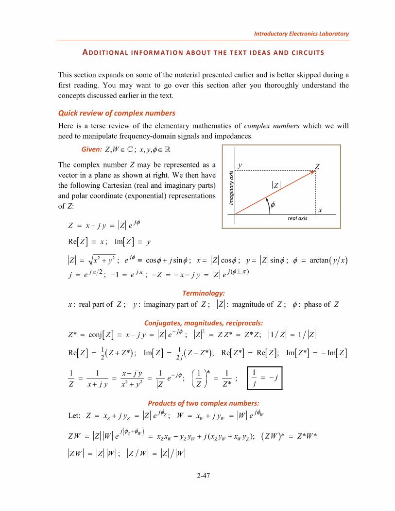
Introductory Electronics Laboratory
2-47
ADDIT IONAL INFORMATION ABOUT T HE T EXT IDEAS AND C IRCUIT S
This section expands on some of the material presented earlier and is better skipped during a first reading. You may want to go over this section after you thoroughly understand the concepts discussed earlier in the text.
Quick review of complex numbers Here is a terse review of the elementary mathematics of complex numbers which we will need to manipulate frequency-domain signals and impedances.
Given: ,Z W ∈ ; , ,x y φ ∈y
The complex number Z may be represented as a vector in a plane as shown at right. We then have the following Cartesian (real and imaginary parts) and polar coordinate (exponential) representations of Z:
jZ x j y Z e φ= + =
[ ]Re Z x≡ ; [ ]Im Z y≡
2 2Z x y= + ; cos sinje jφ φ φ≡ + ; cosx Z φ= ; siny Z φ= ; ( )arctan y xφ = 2jj e = ; 1 je − = ; ( )jZ x j y Z e φ π±− = − − =
Terminology: : real part of ; : imaginary part of ; : magnitude of ; : phase of x Z y Z Z Z Zφ
Conjugates, magnitudes, reciprocals:
[ ] 2* conj ; * * ; 1 1jZ Z x j y Z e Z Z Z Z Z Z Zφ−= ≡ − = = = =
[ ] ( ) [ ] ( ) [ ] [ ] [ ] [ ]1 12 2Re * ; Im * ; Re * Re ; Im * ImjZ Z Z Z Z Z Z Z Z Z= + = − = = −
2 2
1 1 1 1 1*;*
jx j y eZ x j y x y Z ZZ
φ−− = = = = + + ;
1 jj
= −
Products of two complex numbers:
Let: ;Z Z W WWZ jjZ x j y Z e W x j y W e φφ= + = = + =
( ) ( )( ); * * *Z W Z W Z W W ZZ Wj
Z W Z W e x x y y j x y x y Z W Z Wφ φ+
= = − + + =
;Z W Z W Z W Z W= =
x
y
φ
Z
Z
imag
inar
y ax
is
real axis

Experiment 2: Additional information about the text ideas and circuits
2-48
If we consider Z and W to be two vectors, then their scalar and vector products are:
( ) [ ] [ ]( ) [ ]
cos Re * Re *
ˆ ˆ( ) ( ) sin Im *Z W Z WW Z
Z W W ZW Z
Z W Z W Z W Z W x x y y
Z W x y Z W Z W x y x y
φ φ
φ φ
= − = = = +
× × = − = = −
Linear functions and time derivatives:
If F (Z ) is a complex-valued function of its complex argument Z, then we can write: ( ) ( ) ( )F Z u Z j v Z= + , where u and v return real values for every Z
If F (Z ) is also linear, then: ( ) ( ) ( ) ( )F Z F x j y F x j F y= + = + [Note: F (real x) may be complex-valued]
Let time ,t ∈y and let ( ) ( ) ( ),Z t x t j y t= + where ( )x t ∈y and ( ) .y t ∈y Then:
( ) ( ) [ ( ) ( )] ( )d d d dx t j y t x t j y t Z tdt dt dt dt
+ = + = ; Re[ ( )] Re ( )d dZ t Z tdt dt
∴ =
so we may exchange the order of time differentiation and taking the real part. This is a most important result.
Introductory Electronics Laboratory
2-49
Fourier and Laplace transforms
In this section we continue the discussion started early in this text relating time-domain and frequency-domain representations of time-varying functions. This section will be more abstract and mathematically-oriented, but will also describe more general and powerful techniques. Real-valued functions of time (not necessarily periodic) may be represented as complex-valued functions of frequency by using a Fourier transform and its inverse (the pair given here is consistent with our sinusoid representation, equations (2.5) on page 2-10, although more symmetric forms of the transform and its inverse are more common):
2.31 0
/ 2
/ 2
( ) Re ( ) (0)
1 1( 0) ( ) ; (0) ( ) lim ( )T
TT
j t
j t
y t Y e d Y
Y y t e dt Y y t y t dtT
ω
ω
ω ω
ωπ
∞
+
∞
→∞−∞ −
−
= +
≠ = ≡ =
∫
∫ ∫
The y (t ) and Y (ω) in equations (2.31) are called a Fourier transform pair. The first equation converts a phasor function Y (ω) to the actual, time-varying voltage or current y (t ) it represents. The second equation tells how to construct Y (ω) from a given y (t ) (note that Y (0) is the mean value of y (t ), a real number, also called its DC component ). Mathematicians have extensively studied just what sorts of functions can be represented this way and what exactly is meant by the “ = ” in (2.31); we won’t worry about such issues here.
Note that the second equation in (2.31) will give a valid result for Y (ω) even if ω < 0 (negative frequencies) as well as for “normal” positive frequencies. What does it mean if ω < 0, you may ask. There is nothing mysterious here: ω < 0 just means that the phase of the complex integrand ( ) j tY e ωω will decrease with increasing time: the 2-D vector Y(t ) corresponding to this complex function of time will rotate clockwise as t increases, rather than counterclockwise. Since our functions y (t ) are real-valued, it is easy to show that by using the second of equations (2.31) to transform y (t ), we must have Y (–ω) ≡ Y* (ω), so we don’t get any additional information about y (t ) from Y (ω) by including ω < 0 in Y ’s domain of definition. We can just integrate Y over positive ω to get y (t ) as in the first expression in (2.31) (note further that the 0+ lower limit of the integral just means that ω = 0 is not included in its domain).
The transformations (2.31) are linear in y (t ) and Y (ω), so a linear function applied to y (t ) or Y (ω) will transform to some corresponding linear expression for Y (ω) or y (t ), respectively (with the caveat that multiplying Y (ω) by a complex scale factor introduces a phase shift in that frequency component of y (t )). In particular, our very important result (2.8) that
( ) ( )dy t dt j Yω ω⇔ remains valid. As you have already seen from the examples presented earlier in this text, this concept is very useful when you analyze circuits (i.e., networks) with the tools we’ve developed: series and parallel impedances, the voltage divider, loop and node
Experiment 2: Additional information about the text ideas and circuits
2-50
equations, the concepts of input and output impedance, transfer functions, etc. In particular, we have used the complex impedances and frequency responses of a circuit’s various components to calculate a frequency-domain expression for its transfer function, as in equation (2.17) or (2.19). In each case, the algebraic expression for the frequency-domain transfer function can be put into the following form:
2.32 ( )( ) ( ) ( ) ; ( )( )out in
P jY G j Y G jQ j
ωω ω ω ωω
= × =
where P and Q are polynomial functions of their arguments. Note that this relationship implies that Yout(ω) is just proportional to Yin(ω) with (generally) complex proportionality factor G ( jω); this result is a direct consequence of considering only linear circuits.
Note that we’ve written the transfer (gain) function G as a function of jω rather than just ω in (2.32), which is suggestive of what we are going to do next: define the new variable s = jω, so that the transfer function becomes ( ) ( ) ( )G s P s Q s= . Using s as the independent variable, it must be the case that the polynomials P (s) and Q (s) each have only real coefficients (if any common factor of j is divided out of both), because our time-domain input and response functions yin(t ) and yout(t ) must both be real-valued functions of time (you may check that this is indeed the case for the transfer functions derived text).
The zeroes of the two polynomials P and Q (i.e. the solutions sk and sm of P (sk) = 0 and Q (sm) = 0, respectively) are called the zeroes and poles of the transfer function G. These values provide important information about the resonant frequencies, transient behavior, and stability of the dynamical (time-varying) system being modeled. This sort of pole-zero analysis plays a prominent role in analog electrical and control system engineering, and naturally leads to the intense mathematical study of linear dynamical systems using an alternative to our Fourier analysis of equations (2.31): the Laplace transform,
0
( ) ( ) ( ) stY s y t y t e dt∞
−= ≡ ∫L
where now s may take on any complex value (usually expressed as s js ω= + ), and it is assumed that y (t < 0) ≡ 0 (so the input signal to the system is “turned on” at time t = 0).

Introductory Electronics Laboratory
2-51
Power dissipation calculations using phasors
The substitutions in (2.15) on page 2-16 to convert between time- and frequency-domain expressions are generally not valid for nonlinear functions of time such as the power dissipated by a two-terminal element: P (t ) = v (t ) i (t ). DC power dissipation in such an element is, of course, PDC = v DC i DC , but the correct phasor expression for the element’s average AC power dissipation at a particular nonzero angular frequency ω is given by
2.33 [ ] [ ] [ ]2 21 1 12 2 2( ) Re ( )* ( ) ( ) Re ( ) ( ) Re ( )P V I I Z V Y= = =ω ω ω ω ω ω ω
The mean squared voltage and current of a sinusoid with angular frequency ω is given by 21
2 ( )V ω and 212 ( )I ω , respectively. The signal’s root-mean-square (RMS) voltage and
current phasors are thus V (ω) 2/ and I (ω) 2/ . If several sinusoidal signals with different frequencies are present, then the total average power dissipation in the element is just equal to the sum of the powers generated at the various frequencies:
2.34 total DC ( )kk
P P P ω= + ∑
Transformers A transformer is a structure composed of two or more inductors whose coils of wire are wound in very close physical proximity. As a result, the changing magnetic field induced by an oscillating current flowing through one coil is strongly coupled to the other coils. Consequently, a corresponding induced voltage is generated not just in the coil carrying the current but also in each of the other coils, transferring power into circuits attached to the other coils. For example, a transformer is pictured in the upper right corner of Figure 2-4 on page 2-5.
Let’s work out how a transformer does what it does. First consider a single coil of wire forming an inductor. The physics of the electromagnetic field associated with the coil has a simple consequence: everything else being equal, its inductance is proportional to the square of the number of turns of wire n in its coil. This is because the magnetic field generated by the coil has an intensity which is proportional to n, and the resulting voltage across the coil induced by changes in the field is also proportional to n. Thus a coil’s inductance goes as n × n.
Now consider the simple case of two closely-coupled coils with individual inductances L1 and L2 with turn counts n1 and n2. If a current in coil 1 generates a magnetic field which couples into coil 2, then we can define the two coils’ mutual inductance LM as the ratio of the induced voltage in coil 2 caused by changes in the current through coil 1, analogous to our definition of inductance, equation (2.35).
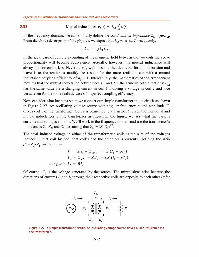
Experiment 2: Additional information about the text ideas and circuits
2-52
2.35 M2 1Mutual inductance: ( ) ( )ddtv t L i t=
In the frequency domain, we can similarly define the coils’ mutual impedance ZM = jωLM. From the above description of the physics, we expect that LM ∝ n1n2. Consequently,
M 1 2L L L∝
In the ideal case of complete coupling of the magnetic field between the two coils the above proportionality will become equivalence. Actually, however, the mutual inductance will always be somewhat less. Nevertheless, we’ll assume the ideal case for this discussion and leave it to the reader to modify the results for the more realistic case with a mutual inductance coupling efficiency of ηM < 1. Interestingly, the mathematics of the arrangement requires that the mutual inductance between coils 1 and 2 is the same in both directions: LM has the same value for a changing current in coil 1 inducing a voltage in coil 2 and vice versa, even for the more realistic case of imperfect coupling efficiency.
Now consider what happens when we connect our simple transformer into a circuit as shown in Figure 2-27. An oscillating voltage source with angular frequency ω and amplitude V1 drives coil 1 of the transformer. Coil 2 is connected to a resistor R. Given the individual and mutual inductances of the transformer as shown in the figure, we ask what the various currents and voltages must be. We’ll work in the frequency domain and use the transformer’s impedances Z1, Z2, and ZM, assuming that ZM = (Z1 Z2)1/2.
The total induced voltage in either of the transformer’s coils is the sum of the voltages induced in that coil by both that coil’s and the other coil’s currents. Defining the ratio ρ2 ≡ Z2/Z1, we then have:
M1 1 1 2 1 1 2
M2 1 2 2 1 1 2
( )( )
V Z I Z I Z I IV Z I Z I Z I I
ρρ ρ
= − = −
= − = −
2 2along with V RI=
Of course, V1 is the voltage generated by the source. The minus signs arise because the directions of currents I1 and I2 through their respective coils are opposite to each other (refer
Figure 2-27: A simple transformer circuit. An oscillating voltage source drives a load resistance via the transformer.
L1 L2
LM
V1 V2 R
I1 I2

Introductory Electronics Laboratory
2-53
again to Figure 2-27), and there for the magnetic fields they generate are also oppositely directed.
So we have three equations for the two unknown currents and for the resistor voltage V2. Assuming that I1 ≠ ρ I2, the ratio of the first two equations above requires that V2/V1 = ρ. In terms of the number of turns in each coil, since Z ∝ n2, ρ is conventionally called the transformer’s turns ratio. The “turns ratio” is then the ratio of the voltages across the transformer’s two coils. Ohm’s law for the load resistor R then immediately gives I2:
2 12
V VI
R Rρ= =
Substituting back into the equation for V1 gives I1:
2
1 11
1I VZ R
ρ = +
So the load impedance seen by the source supplying V1 turns out to be the parallel combination of the coil’s impedance, Z1 = jωL1, and the load resistance divided by the square of the turns ratio, R /ρ2. Because Z1 has some finite value, we see that our assumption that I1 ≠ ρ I2 is justified. On the other hand, to transfer power to the load resistor R most efficiently one would not want an imaginary part to the impedance that is presented to the source. This means that an efficient transformer should have |Z1| = ωL1 R /ρ2, or, equivalently, ωL2 R. In the limit that |Z1| → ∞ , then I1 → ρ I2, but their product remains constant so that V2/V1 = ρ is maintained. In this case we also see that the load resistance R is transformed by the square of an ideal transformer’s turns ratio to determine the load presented to the source:
22 1
2 1
V VI I
ρ=
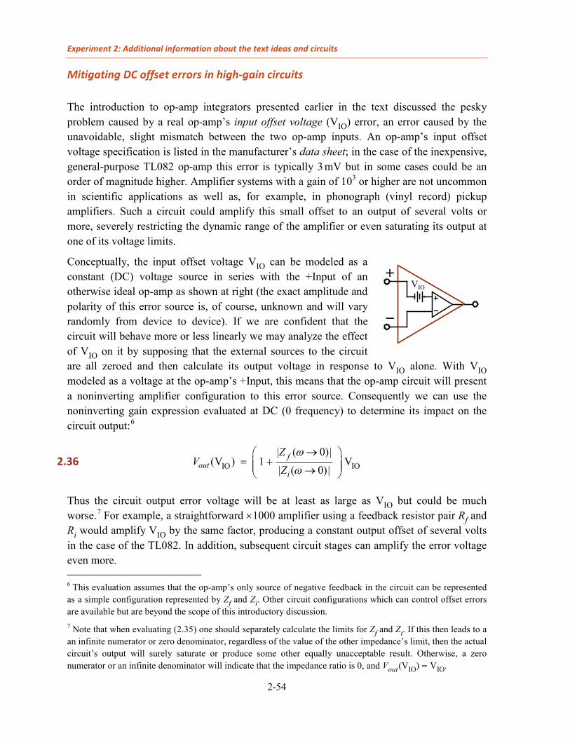
Experiment 2: Additional information about the text ideas and circuits
2-54
Mitigating DC offset errors in high-gain circuits
The introduction to op-amp integrators presented earlier in the text discussed the pesky problem caused by a real op-amp’s input offset voltage (VIO) error, an error caused by the unavoidable, slight mismatch between the two op-amp inputs. An op-amp’s input offset voltage specification is listed in the manufacturer’s data sheet; in the case of the inexpensive, general-purpose TL082 op-amp this error is typically 3 mV but in some cases could be an order of magnitude higher. Amplifier systems with a gain of 103 or higher are not uncommon in scientific applications as well as, for example, in phonograph (vinyl record) pickup amplifiers. Such a circuit could amplify this small offset to an output of several volts or more, severely restricting the dynamic range of the amplifier or even saturating its output at one of its voltage limits.
Conceptually, the input offset voltage VIO can be modeled as a constant (DC) voltage source in series with the +Input of an otherwise ideal op-amp as shown at right (the exact amplitude and polarity of this error source is, of course, unknown and will vary randomly from device to device). If we are confident that the circuit will behave more or less linearly we may analyze the effect of VIO on it by supposing that the external sources to the circuit are all zeroed and then calculate its output voltage in response to VIO alone. With VIO modeled as a voltage at the op-amp’s +Input, this means that the op-amp circuit will present a noninverting amplifier configuration to this error source. Consequently we can use the noninverting gain expression evaluated at DC (0 frequency) to determine its impact on the circuit output:6
2.36 IO IO| ( 0)|
(V ) 1 V| ( 0)|
fout
i
ZV
Zω
ω
→ = + →
Thus the circuit output error voltage will be at least as large as VIO but could be much worse.7 For example, a straightforward ×1000 amplifier using a feedback resistor pair Rf and Ri would amplify VIO by the same factor, producing a constant output offset of several volts in the case of the TL082. In addition, subsequent circuit stages can amplify the error voltage even more. 6 This evaluation assumes that the op-amp’s only source of negative feedback in the circuit can be represented as a simple configuration represented by Zf and Zi. Other circuit configurations which can control offset errors are available but are beyond the scope of this introductory discussion. 7 Note that when evaluating (2.35) one should separately calculate the limits for Zf and Zi. If this then leads to a an infinite numerator or zero denominator, regardless of the value of the other impedance’s limit, then the actual circuit’s output will surely saturate or produce some other equally unacceptable result. Otherwise, a zero numerator or an infinite denominator will indicate that the impedance ratio is 0, and Vout(VIO) = VIO.
VIO
+
−

Introductory Electronics Laboratory
2-55
One can mitigate the effect of VIO on the circuit’s output by ensuring that (2.36) gives a tolerable result for its output offset error. If the amplifier does not need to respond all the way down to constant (DC) signals, but has some minimum signal frequency of interest fmin, then the solution is simple: make sure that Zi(ω→0) = ∞ by adding a capacitor in series with the other elements making up Zi: Figure 2-28 shows an example. This circuit behaves somewhat like an amplifier with an added AC coupling, high-pass filter on its input. In this case, however, the filter is incorporated into the feedback network so that it also affects the amplification of VIO. This is actually the same circuit as the AC coupled inverting amplifier shown in Figure 2-25, except that it is used in its noninverting configuration. We now see how the inverting amplifier configuration can also greatly reduce the effect of VIO but not eliminate it: VIO will still show up as a small output offset.
One final note: the circuit of Figure 2-28 does not necessarily replace the need for an AC coupling high-pass filter (Figure 2-9 on page 2-20). At DC the circuit of Figure 2-28 has a gain of 1, so a large DC component in the input signal will not be eliminated from its output.
Figure 2-28: Mitigating the effect of VIO on a high-gain amplifier’s output. At DC, the infinite impedance of Ci reduces the noninverting amplifier’s gain to unity. On the other hand, input signals well above f0 = 1/(2πRiCi), the RC corner frequency, are unaffected – the gain within the passband is G = 1 + (Rf /Ri).
Ri
Rf
Ci
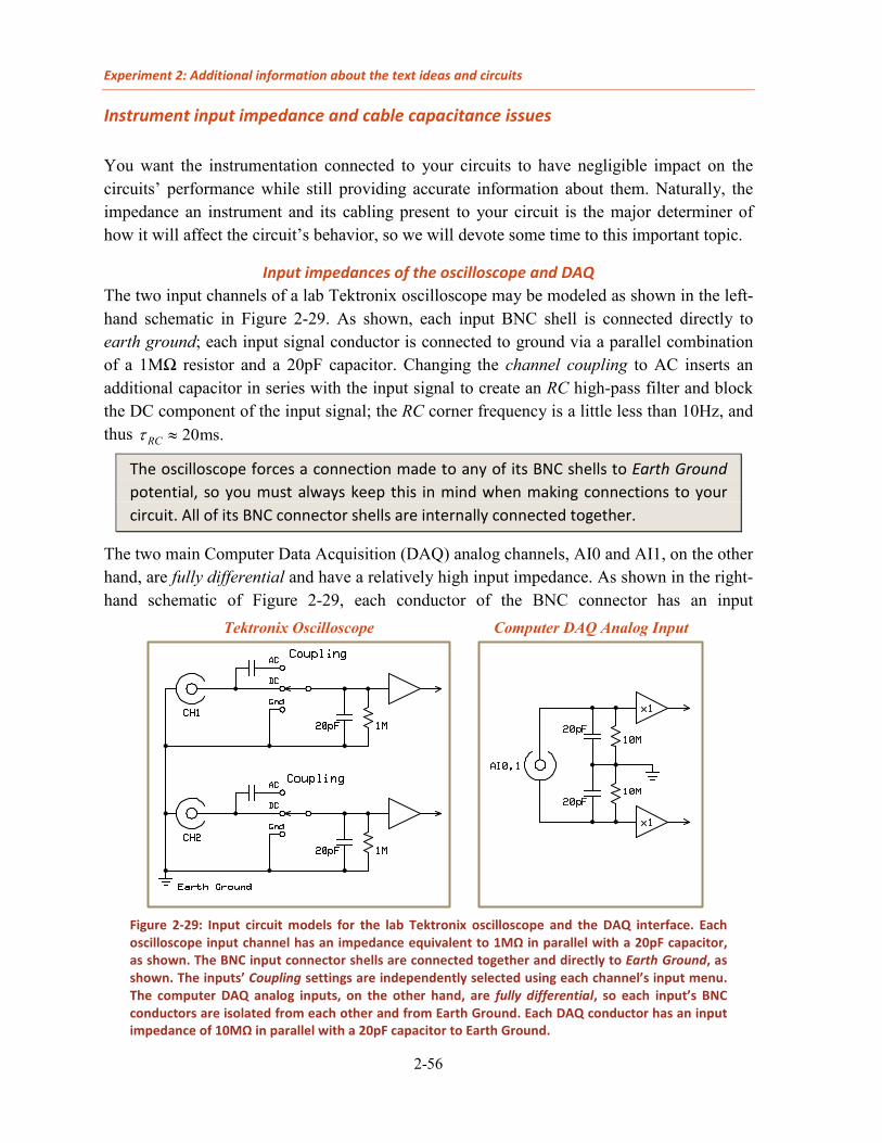
Experiment 2: Additional information about the text ideas and circuits
2-56
Instrument input impedance and cable capacitance issues
You want the instrumentation connected to your circuits to have negligible impact on the circuits’ performance while still providing accurate information about them. Naturally, the impedance an instrument and its cabling present to your circuit is the major determiner of how it will affect the circuit’s behavior, so we will devote some time to this important topic.
Input impedances of the oscilloscope and DAQ The two input channels of a lab Tektronix oscilloscope may be modeled as shown in the left-hand schematic in Figure 2-29. As shown, each input BNC shell is connected directly to earth ground; each input signal conductor is connected to ground via a parallel combination of a 1MΩ resistor and a 20pF capacitor. Changing the channel coupling to AC inserts an additional capacitor in series with the input signal to create an RC high-pass filter and block the DC component of the input signal; the RC corner frequency is a little less than 10Hz, and thus 20ms.RCt ≈
The oscilloscope forces a connection made to any of its BNC shells to Earth Ground potential, so you must always keep this in mind when making connections to your circuit. All of its BNC connector shells are internally connected together.
The two main Computer Data Acquisition (DAQ) analog channels, AI0 and AI1, on the other hand, are fully differential and have a relatively high input impedance. As shown in the right-hand schematic of Figure 2-29, each conductor of the BNC connector has an input
Tektronix Oscilloscope Computer DAQ Analog Input
Figure 2-29: Input circuit models for the lab Tektronix oscilloscope and the DAQ interface. Each oscilloscope input channel has an impedance equivalent to 1MΩ in parallel with a 20pF capacitor, as shown. The BNC input connector shells are connected together and directly to Earth Ground, as shown. The inputs’ Coupling settings are independently selected using each channel’s input menu. The computer DAQ analog inputs, on the other hand, are fully differential, so each input’s BNC conductors are isolated from each other and from Earth Ground. Each DAQ conductor has an input impedance of 10MΩ in parallel with a 20pF capacitor to Earth Ground.
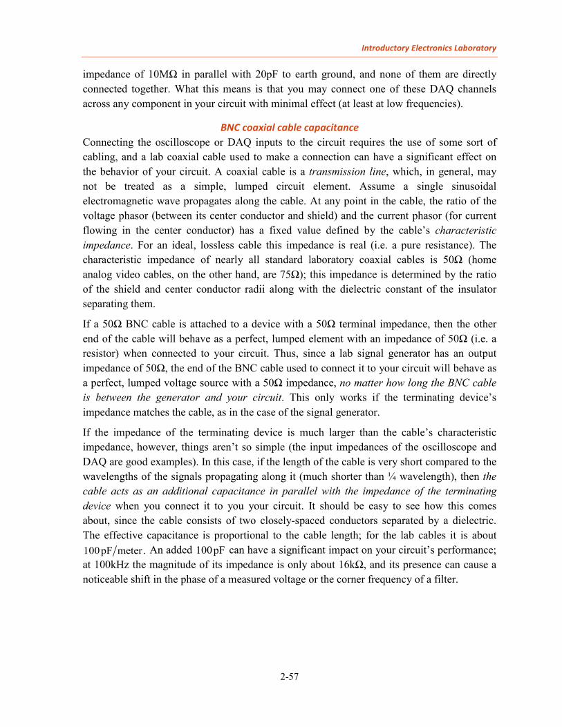
Introductory Electronics Laboratory
2-57
impedance of 10MΩ in parallel with 20pF to earth ground, and none of them are directly connected together. What this means is that you may connect one of these DAQ channels across any component in your circuit with minimal effect (at least at low frequencies).
BNC coaxial cable capacitance Connecting the oscilloscope or DAQ inputs to the circuit requires the use of some sort of cabling, and a lab coaxial cable used to make a connection can have a significant effect on the behavior of your circuit. A coaxial cable is a transmission line, which, in general, may not be treated as a simple, lumped circuit element. Assume a single sinusoidal electromagnetic wave propagates along the cable. At any point in the cable, the ratio of the voltage phasor (between its center conductor and shield) and the current phasor (for current flowing in the center conductor) has a fixed value defined by the cable’s characteristic impedance. For an ideal, lossless cable this impedance is real (i.e. a pure resistance). The characteristic impedance of nearly all standard laboratory coaxial cables is 50Ω (home analog video cables, on the other hand, are 75Ω); this impedance is determined by the ratio of the shield and center conductor radii along with the dielectric constant of the insulator separating them.
If a 50Ω BNC cable is attached to a device with a 50Ω terminal impedance, then the other end of the cable will behave as a perfect, lumped element with an impedance of 50Ω (i.e. a resistor) when connected to your circuit. Thus, since a lab signal generator has an output impedance of 50Ω, the end of the BNC cable used to connect it to your circuit will behave as a perfect, lumped voltage source with a 50Ω impedance, no matter how long the BNC cable is between the generator and your circuit. This only works if the terminating device’s impedance matches the cable, as in the case of the signal generator.
If the impedance of the terminating device is much larger than the cable’s characteristic impedance, however, things aren’t so simple (the input impedances of the oscilloscope and DAQ are good examples). In this case, if the length of the cable is very short compared to the wavelengths of the signals propagating along it (much shorter than ¼ wavelength), then the cable acts as an additional capacitance in parallel with the impedance of the terminating device when you connect it to you your circuit. It should be easy to see how this comes about, since the cable consists of two closely-spaced conductors separated by a dielectric. The effective capacitance is proportional to the cable length; for the lab cables it is about 100pF meter. An added 100pF can have a significant impact on your circuit’s performance; at 100kHz the magnitude of its impedance is only about 16kΩ, and its presence can cause a noticeable shift in the phase of a measured voltage or the corner frequency of a filter.

Experiment 2: Additional information about the text ideas and circuits
2-58
Connecting a BNC coaxial cable between a circuit and a device with a 50Ω impedance acts as if the 50Ω is connected directly into the circuit (by design!). Connecting a BNC cable between a circuit and a high impedance instrument adds a capacitance of 100pF/meter to the circuit in parallel with the device’s input impedance.
So how can you mitigate the effect of this additional capacitance caused by adding a coaxial cable? One simple way is to buffer the cable connection using a voltage follower, as shown in Figure 2-30. The high input impedance of the voltage follower isolates the connection from your circuit, and a TL082 op-amp can successfully drive the capacitance of coaxial cables with lengths of several meters, especially if you add an output load resistor to the follower circuit as shown.
Figure 2-30: Using a voltage follower to buffer a coaxial cable connection. The high impedance of the follower’s input has minimal effect on the circuit being monitored (the “test point”), and its low output impedance can drive the capacitance of a fairly long 50Ω coax connected to a high impedance instrument. The 560Ω load resistor on the follower reduces overshoot and ringing in its output when driving a long cable’s capacitive load.
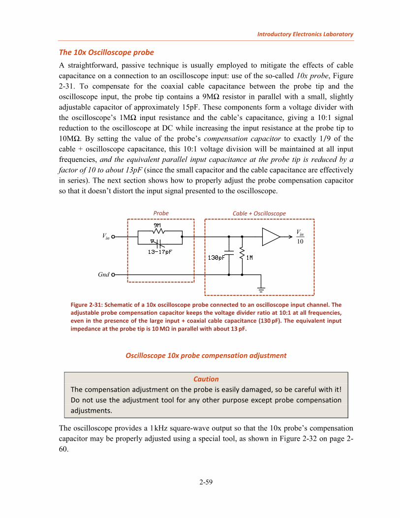
Introductory Electronics Laboratory
2-59
The 10x Oscilloscope probe A straightforward, passive technique is usually employed to mitigate the effects of cable capacitance on a connection to an oscilloscope input: use of the so-called 10x probe, Figure 2-31. To compensate for the coaxial cable capacitance between the probe tip and the oscilloscope input, the probe tip contains a 9MΩ resistor in parallel with a small, slightly adjustable capacitor of approximately 15pF. These components form a voltage divider with the oscilloscope’s 1MΩ input resistance and the cable’s capacitance, giving a 10:1 signal reduction to the oscilloscope at DC while increasing the input resistance at the probe tip to 10MΩ. By setting the value of the probe’s compensation capacitor to exactly 1/9 of the cable + oscilloscope capacitance, this 10:1 voltage division will be maintained at all input frequencies, and the equivalent parallel input capacitance at the probe tip is reduced by a factor of 10 to about 13pF (since the small capacitor and the cable capacitance are effectively in series). The next section shows how to properly adjust the probe compensation capacitor so that it doesn’t distort the input signal presented to the oscilloscope.
Figure 2-31: Schematic of a 10x oscilloscope probe connected to an oscilloscope input channel. The adjustable probe compensation capacitor keeps the voltage divider ratio at 10:1 at all frequencies, even in the presence of the large input + coaxial cable capacitance (130 pF). The equivalent input impedance at the probe tip is 10 MΩ in parallel with about 13 pF.
Oscilloscope 10x probe compensation adjustment
Caution The compensation adjustment on the probe is easily damaged, so be careful with it! Do not use the adjustment tool for any other purpose except probe compensation adjustments.
The oscilloscope provides a 1kHz square-wave output so that the 10x probe’s compensation capacitor may be properly adjusted using a special tool, as shown in Figure 2-32 on page 2-60.
Probe Cable + Oscilloscope
inV10
inV
Gnd
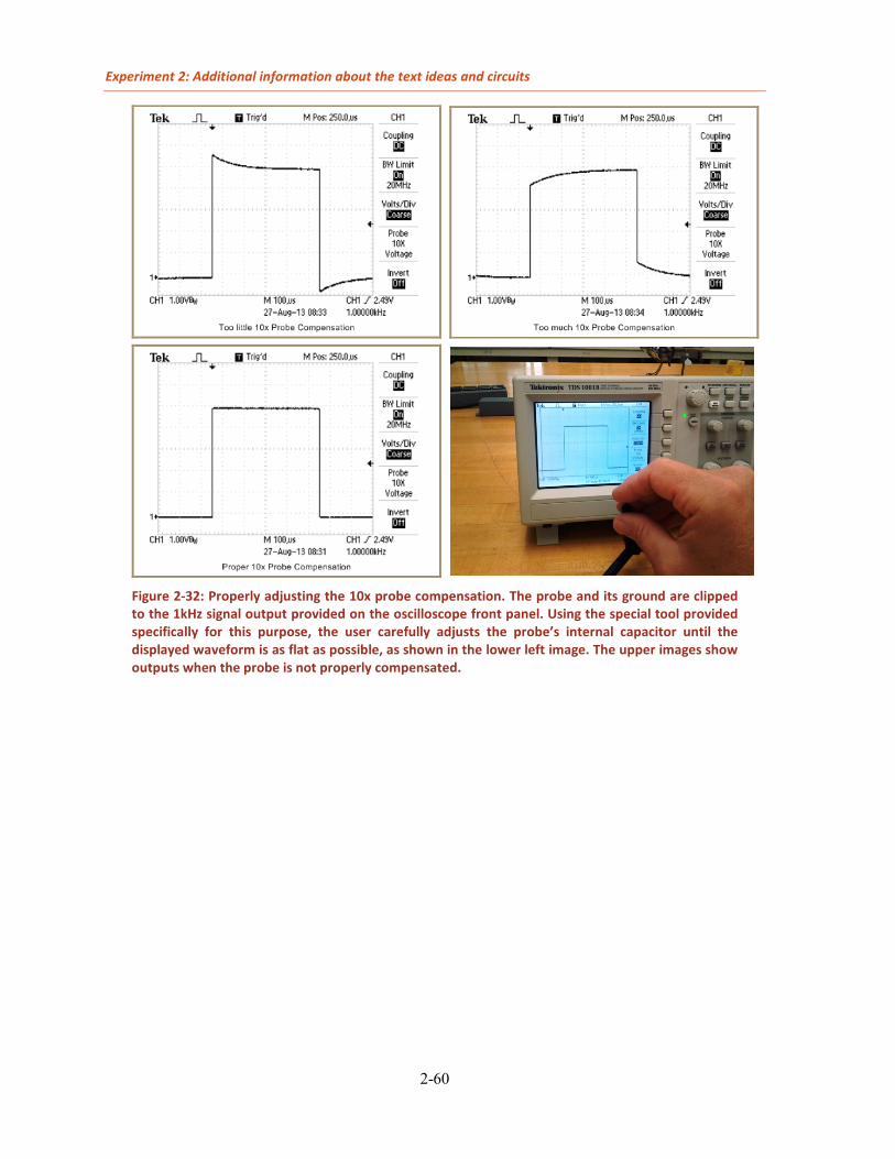
Experiment 2: Additional information about the text ideas and circuits
2-60
Figure 2-32: Properly adjusting the 10x probe compensation. The probe and its ground are clipped to the 1kHz signal output provided on the oscilloscope front panel. Using the special tool provided specifically for this purpose, the user carefully adjusts the probe’s internal capacitor until the displayed waveform is as flat as possible, as shown in the lower left image. The upper images show outputs when the probe is not properly compensated.