experimental collision physics - school of physical sciences - dcu
TRANSCRIPT

1
Experimental Collision Physics
Session III
QuAMP II Summer School,Milton Keynes
Wednesday, 21st September, 2005.

2
Lectures in this session arepresented by
members of the
Atomic and Molecular Interactions GroupInstitute of Physics.

3

4
Table of Contents.
Section 1. Introduction. Collision physics - an overview Page 5
Section 2.1 Atomic & molecular Beam Sources Page 8
Section 2.2 Atomic beam sources for unstable atomic species Page 20
Section 3.1 Ion sources Page 22
Section 3.2 Electron sources Page 26
Section 3.3 Electron guns & electrostatic lenses Page 29
Section 4. Electron energy analysers Page 36
Section 5. Detection of single particles & associated electronics Page 41
Section 6. Coincidence and counting techniques Page 54
Section 7. Data and signal analysis Page 61
Appendix 1 Data sheets for section 3.
Appendix 2 Data sheets for section 5.
Appendix 3 Data sheets for section 6.
Appendix 4 Data sheets for section 7.

5
1. Collision Physics – An Overview.
1.1 Outline.
Collision physics includes ANY collision of a quantum particle with a target.
Collision Particles may be:
••••• PHOTONS (eg from a Laser, Synchrotron source or FEL)
••••• ELECTRONS (usually of well defined momentum from an electron gun)
••••• IONS (usually from an ion source of well defined momentum)
••••• NEUTRAL PARTICLES (often in an excited state, eg metastable atoms)
••••• POSITRONS (although we are not talking about these today)
TARGETS may include:
••••• ATOMS (usually in ground state, a laser excited state or a metastable state)
••••• MOLECULES (as with atoms)
••••• CLUSTERS (usually produced in an ultra-cold target preparation)
••••• IONS (from an ion source)
••••• TRAPPED ATOMS (eg in a Magneto-Optical Trap)
••••• TRAPPED IONS (eg in a Paul Trap, or an Ion Storage Ring)
TARGETS almost always in GAS PHASE (but collisions with solids also carried out)
Why study collisions in detail?
••••• Experimental test of fundamental interactions between quantum particles – eg long rangeCoulombic interaction between charged particles.
••••• Develop theoretical understanding of these interactions over a wide energy range (fromthreshold to very high impact energies) for all scattering geometries.
Apply models & experimental results to real situations in eg:
••••• Lasers••••• Astrophysics••••• Upper & Lower Atmospheric physics••••• Bio-physics••••• Chemistry••••• Surface & Materials Science••••• Lighting••••• Engineering (ion sputtering, nanofabrication)
To name a few.
ANYWHERE that collisions between atoms, molecules, photons, electrons and ionsoccur can be studied experimentally & theoretically (in principle).

6
1.2 Basic Experimental setup for study of collisions.
Incident particle of well controlled momentum reacts with target.
INTERACTION occurs with target. This interaction may be:
••••• Elastic collision••••• Inelastic collision leading to target excitation••••• Ionization of target••••• Capture of incident particle by target
Following the interaction several particles may appear in outgoing channel.
Study details of these particles (in asymptotic limit) to ascertain what happened in the reaction zone.
Details which are studied include:
••••• Final momentum of scattered, ejected particles.••••• Fragmentation of target.••••• Spin state of final particles.••••• Ionization of target or incident projectile.
It is the AIM of collision physics to ascertain what happened in the interaction zoneto produce these final products.
ESSENTIAL that experiments are carried out to high precision.
ESSENTIAL that theoretical models of the interaction are sophisticated enoughto accurately model the experimental results.
NO MODEL AT PRESENT AGREES WITH EXPERIMENTOVER ALL ENERGIES & ALL GEOMETRIES.
EXPERIMENTS ARE BECOMING INCREASINGLY SOPHISTICATED TODETAIL THESE INTERACTIONS MORE CLOSELY.
It is the purpose of this session to outline how these experiments are carried out,& to provide insight into existing and new techniques being used.
Target
InteractionRegion
Incident particle
Particlesresulting
fromInteraction
e.g. ions, electrons,photons
FIG 1. Collisional interaction between an incident particle & a target, resulting in scattered & ejected particles whosecharacteristics (momentum, spin, energy etc) are measured in detail.

7
1.3 Session Timetable.
9.00am - 10.00am
1. Introduction. (5 minutes)
2. Beam Sources – Preparation of the target for study. (20 minutes).
3. Electron & ion sources – how to prepare & manipulate an incident beam. (20 minutes)
4. Analysers –measuring the particles following the interaction. (15 minutes)
10.00am - 10.30am Coffee & Tea break
10.30am - 12.00 noon
5. Detectors - how are single quantum particles detected? (20 minutes)
6. Counting techniques – how to ascertain the reaction dynamics. (20 minutes)
7. Data analysis – how to analyse different results & techniques. (20 minutes)
8. General discussion - open forum on all topics discussed today. (30 minutes)

8
2.1 Atomic & Molecular Beam SourcesDr Andrew Murray,
University of Manchester, Manchester M13 9PL, UK.Email: [email protected].
2.1 Introduction.
Time constraints mean can only discuss small subset of all different sources.
Going to select the following types (with examples from work being carried out in Manchester):
••••• Atomic beam sources••••• Molecular beam sources••••• Cold atomic beam sources & targets
Each has different configurations & requirements.
Basic aim of all beam sources:
To provide a bright target beam which is collimated, and has high density.
These criteria can be very difficult to achieve in practice!
Most experiments require high target density in interaction region as phenomena to be studiedoften have very small cross section (measured by probability of detection).
SOMETIMES beam density must be limited due to collisions.
e.g. RADIATION TRAPPING: Experiments involving radiation from ground state targets needto limit target beam density in interaction region.
Trapping occurs since photons emitted by an excited target may be absorbed by another target,photons then being re-released in random direction (multiple scattering).
Reduces information which can be obtained from system under study.
FIG 1. Radiation trapping in target beams of high density. The excited atom radiates a photon which is absorbed and re-radiated by a second & third atom. Information on the direction & polarization of the initial photon may then be lost.
Hence density of the source must be chosen carefully.
Spon
tane
ous
Em
issi
onPhotonelectronexcitation
ATOM 1 ATOM 2
Spon
tane
ous
Em
issi
on
Abs
orpt
ion
Spon
tane
ous
Em
issi
onPhoton
ATOM 3
Abs
orpt
ion
PhotonDetector
No Correlation in Direction, Polarization

9
2.1.1 The Interaction Region.
Interaction region is defined as volume of space where reaction occurs – this may be with anelectron, an ion, a neutral excited particle or a laser beam.
Interaction region must be WELL DEFINED IN SPACE (typical size ~1mm3), so momenta ofthe reaction products are accurately known.
For collision experiments, momenta and energy of reaction products often measured INCOINCIDENCE –products must come from same target.
Interaction region usually governed by target beam profile, incident electron/ion/laser beamprofile, or using lenses (electrostatic or optical) in experiment. Gun, Analysers must be positionedaccurately (see eg Murray et al, Meas Sci Tech 16, N19 (2005).)
2.2 Atomic beams.
Atomic beams mostly come in two different types:
2.2.1 Effusive gas sources.
Produced from a capillary (nozzle) which directs atoms into interaction region.
This is the simplest beam delivery system possible.
FIG 2. The interaction region defined by the target beam, electron/ion beam and the optics used in the experiment. Inthis case, an (e,2e) experiment is shown. The target is ionised, leaving two electrons to be detected in coincidence.
FIG 3. Simple capillary (nozzle) used to deliver atoms/molecules in the gas phase to the interaction region.
CapillaryRedirectionchamber
Atomic Beam
Gas FeedFrom External
Gas Bottle
InteractionRegion
Incident Electron detected
electronsξ
ξ
E2
E1
2
1
k1
k2
k0 Einc
CapillaryNozzle
Atomic/MolecularBeam
InteractionRegion
Scattering Plane

10
Capillary may include array of micro-capillaries –improves target density BUT they areexpensive [see eg Buckman S J et al 1993 Meas. Sci. Tech. 4 1143].
FIG 4. Micro-capillary array to deliver high density of atoms/molecules in the gas phase to the interaction region.
Capillary almost always constructed of NON-MAGNETIC material
Use materials such as:
••••• Molybdenum (excellent for low energy electron scattering - expensive)••••• Platinum-Iridium (good tensile strength - expensive)
Stainless steel nozzles NOT generally used, as manufacture usually makes these slightlyMAGNETIC. – NOT GOOD for low energy electron collisions!
Capillary arrays usually GOLD COATED to reduce charge build up on insulating surfaces – careis therefore required when using these.
2.2.1.1 Quality of target beam from capillaries.
Delivery from a capillary is reasonably good but angular spread is relatively high (depends ondriving pressure, type of gas used, quality of output orifice, length of tube).
FIG 5. Angular spread of target beam delivered from single capillary & micro-capillary arrays, showing the improve-ment possible with a mutliple array of nozzles (from Buckman et al MST 4, 1143 (1993)).
CapillaryAtomic Beam
Micro-arrayGas Feed
Capillary delivery systems usually used for atoms & molecules in gas phase, eg:
• Helium, Argon, Neon, Krypton, Xenon• Molecules: eg H
2, CO
2, N
2 etc.
Advantages of capillaries:
• Cheap & easy to construct• Reliable• High density easily achieved
0
0.2
0.4
0.6
0.8
1
1.2
-40 -20 0 20 40
Inte
nsity
(N
orm
alis
ed to
uni
ty)
Beam Angular Divergence (deg)
22° FWHM
41° FWHM
Micro-CapillaryArray
Single Capillary

11
Disadvantages of capillaries:
• Poor beam quality• May produce radiation trapping problems• Only useful for targets in gas phase at room temperature & in vacuum
2.2.2 Target Beam Ovens.
Target Beam Ovens used when atoms/molecules are in solid or liquid phase (eg Hg) in vacuum atroom temperature.
Oven heats sample to enter gas phase – this may occur through a liquid transition or directly throughsublimation.
Heated targets in gas phase usually emitted into interaction region through capillary nozzle –oftenuse Molybdenum as it has very high melting temperature.
Many different designs of oven are possible.
For an excellent review see Ross & Sonntag, Rev. Sci. lnst. 66 (1995) p4409.
Design depends on whether maximum density is priority, or whether collimation is a priority.
Design types include:
••••• Directly heated ovens (often using thermo-coax) – Temp up to 2000K possible••••• Indirectly heated ovens (eg by electron bombardment, RF heating) – Temp >2500K possible••••• Re-circulating ovens (excellent beam quality, reduced density) – only used for atoms which
have a liquid phase, eg Na, K, Rb, Li, Cs, Mg.
Second type not often used as it is difficult to eliminate RF fields & electrons emitted fromheating process.
2.2.2.1 Directly heated ovens.
Example: Calcium oven used at Manchester (Cvejanovic & Murray, M.S.Tech. 13, p1482 (2002)).
FIG 6. The directly heated calcium oven used in (e,2e) coincidence studies at Manchester. The crucible and nozzleheaters are copper jackets wound with Thermo-coax. The seal is a stainless steel plug close fitted onto astainless steel
edge. The capillary nozzle is molybdenum, internal diameter 1.4mm.
Calcium pellets
Heat Shields
Heat Shields
Heat ShieldsSeal Crucible Heater Jacket
Nozzle Heater Jacket

12
• T ~ 1000K in this design.• Use of heat shields to reduce energy needed to heat oven.• Use of two heaters (body + nozzle). – Ensures output capillary is hotter than main crucible.• Use of high stability constant current supplies for heaters – ensures constant temperature
of all oven parts.• Use of monitoring thermo-couples for accurate temperature assessment.••••• Calcium charge loaded in argon – important for volatile substances (explosive in air).••••• Oven seal is S/S to S/S – need to test design for reaction at high temperatures! (eg Ca + Cu
seal rapidly destroys Cu seal, & may destroy oven).
IMPORTANT:
Stainless Steel for oven is 310 grade – do NOT use 316, 304 grades due to poor magneticproperties of these grades.
Output capillary is Molybdenum – non magnetic, high temperature.
Output beam characteristics from Calcium oven is poor, due to re-scattering inside capillary.Necessary as high densities in interaction region are essential for these experiments.
Optimise target beam density in interaction region by monitoring experiment while trying toeliminate deposition of calcium throughout vacuum chamber.
Deposition causes major difficulties for low energy electron experiments.
Advantages of directly heated ovens:
• Relatively simple to construct.• Relatively low cost.• Easy to operate.• Produces target beam from atoms/molecules in solid, liquid phase at room temperature.
Disadvantages of directly heated ovens:
• Difficult to control beam quality in interaction region.• Low yield & low beam density.• Heating may cause problems in vacuum chamber.• Deposition of target onto sensitive components (eg lens elements) can be major problem.
May require frequent intervention & cleaning.• Some targets may explode on contact with air – can be quite exciting when opening vacuum
system.
2.2.2.2 Re-circulating Ovens.
• Complex & involved oven design which may have significant advantages.• Used for targets which pass through liquid phase prior to gas phase.
• Re-circulating oven designs use condenser to re-liquify unused atoms/molecules, redirectingthese back to crucible.

13
ONLY atoms/molecules which pass through an output aperture in condenser become targetbeam – produces well collimated beam at interaction region.
Advantages of re-circulating ovens:
••••• Charge in crucible lasts much longer••••• Target Beam very well collimated••••• Contamination of vacuum chamber markedly reduced.
Disadvantages of re-circulating ovens:
••••• Control of oven working parameters very difficult – temperatures need to be within closetolerances throughout oven.
••••• Procedure for heating and cooling of different oven components must be carefully controlled.••••• Beam delivery must be horizontal – due to drops falling onto nozzle & subsequent oven
vomiting!••••• Only limited number of atoms can be used.
Example: The re-circulating potassium oven at Manchester.
• Note use of individual heaters with associated heat shields around different oven parts.• Note use of liquid oil cooled condenser – achieves close temperature control even when
atomic beam liquefies onto condenser (problem with alkali’s which have high heat conduction).••••• Collimation achieved by nozzle + condenser aperture sizes + spacing – beam angle is only
3° for this K oven.• Used in new atom beam source of cold atoms (see below).
FIG 7. The re-circulating potassium oven at Manchester, which uses a thermal bath of liquid silicon oil passing aroundthe condenser to ensure excellent thermal control of the re-liquification process of the effusing atoms.
Collimated OutputBeam
Condensation Chamber
Silicon OilFeed/Return
Copper Heater Jacket (top plate not Shown)
Heaters
Pota
ssiu
m
Crucible +Thermo-coax
MountingPoint
recirculatingPipe
Potassium Spray
NozzleCollimating
Aperture
Copper Jacket(oil Temperature)
Liquid potassiumcatchment funnel
Pipe
Tem
pera
ture
Gra
dien
t
T ~ 400°C
T ~ 70°C
Hea
ter
Cur
rent

14
2.3 Molecular beam Sources.
Two main types used – Capillary sources (as above) & Supersonic sources.
For easy delivery, use a simple capillary source as it is cheap.For COLD molecular beams, generally use supersonic sources.
2.3.1 Supersonic Molecular Beams.
Molecules can have extremely complex energy levels due to:
• Electronic levels• Vibrational levels• Rotational levels
To simplify an experiment and for comparison to theory, advantageous to reduce number of energylevels in target as much as possible.
Can be achieved by COOLING the molecules (reduces their internal energy)
Cooling usually achieved in a supersonic expansion of the target gas.
Supersonic expansion occurs when high pressure gas (1 – 2 atm) is released through small apertureinto high vacuum (typically ~ 10-8 torr background pressure).
Multiple collisions occur in expansion phase – leads to high translational velocity with low internalenergy of individual molecules.
With correct operation, only the lowest (v, J) = (0, 0) state is populated.
Supersonic expansion usually occurs in source chamber separated from interaction chamber.Source chamber requires a high speed pump to quickly remove unused gas.
Supersonic nozzles are usually PULSED to reduce the load on the pumps
FIG 8. Supersonic nozzle as used in pulsed laser/electron experiments at Manchester. The nozzle uses a peizo-electricflexure assembly to rapidly pulse the nozzle at up to 200Hz.
Nozzle
OutputAperture
HT Input
Gas Inlet
Valve Body
Valve Face
Nozzle Seal
Supersonic Expansion

15
Supersonically cooled molecular beam is usually skimmed prior to interaction region – this processcollimates molecular beam at interaction region.
Skimmer often used to separate interaction chamber from source chamber.
Typical speeds of supersonic beam depends on target:
• He ~ 1800m/s • H2 ~ 2000m/s • N
2 ~ 800m/s
Translational speed distribution also well defined, typically 5% – 10% of translation speed.
FIG 9. Exponentially flared skimmer used to collimate the supersonic molecular beam prior to passing to the interac-tion chamber. The skimmer orifice is 1mm, the thickness of the skimmer metal being 5µm at the orifice.
Example: Supersonic beam delivery system at Manchester used for laser experiments.
FIG 10. Speed distribution from supersonic expansion of He, fitted to experiment. The expansion produces a beam ofspeed ~ 1750m/s with a width around 6% of the average.
FIG 11. The source chamber used in Manchester for supersonic expansion. The skimmer is located 150mm from thenozzle to ensure collimation of the beam into the interaction chamber.
0
0.2
0.4
0.6
0.8
1
1.2
1000 1500 2000 2500
Bea
m I
nten
sity
(A
rb U
nits
)
Beam Velocity (m/s)
Peak Velocity = 1750m/s
FWHM ~ 100m/s
Speed = Mach 20
Source Chamber
Skimmer
Pulsed Nozzle
Loc
ate
skim
mer
1mm Nozzle Su
pers
onic
E
xpan
sion
Flange of Interaction Chamber
250mmDiffusion Pump
Coupling Flange (310 S/S)Skimmer
Interaction Chamber Bottom Flange
Supersonic Expansion
Top of Nozzle
Target Supersonic Beam
1mm Aperture
O Ring Face

16
••••• Note use of large 250mm diffusion pump in source chamber (much faster recovery to highpressure loads than turbo pumps)
••••• Note use of separate source chamber from interaction chamber – ensures differentialpumping & high vacuum in interaction region.
••••• Nozzle is pulsed up to 200Hz – timing of pulse accurately controlled to ensure overlap ofelectron beam, laser beams, detectors in interaction region.
• By careful design of nozzle & pressure, clusters can be formed for experiments involvingvan der Waals interactions.
Details on different designs can be found in the literature.
2.4 Laser Cooled & Trapped Targets.
Laser cooling & trapping techniques now being used to produce ultra-cold atomic targets (lowtranslational energy).
Technique can produce either a slow beam of atoms or targets can be confined in a Magneto-OpticalTrap (MOT).
Advantages of cold targets:
••••• Well collimated beams possible with very high density.• Virtually no Doppler profile associated with beam source.
FIG 12. Source & interaction chambers used for combined laser & electron collision experiments at Manchester. Thewell defined momentum of the target allows target deflection following electron collision to be determined by the
metastable detector on the vertical rotating table. (Murray & Hammond, Adv. At. Mol. Opt. Phys. 47, p163 (2001)).
Rotation
2500 l/sDiffusion Pump
Electron Gun
Faraday Cup
MetastableDetector
Vertical Rotating
Table
Source Chamber
Interaction Vacuum Chamber
µ-metal Internal Lining
TurboPump
Laser Alignment FlangeBrewsterWindow
ElectricalFeedthroughs Gasline
FeedthroughNozzle electricalFeedthrough
1mm
Skim
mer
Pulsed Nozzle
Supersonic Expansion
Bottom flangeBase-plate
C
B
A
A = Source ChamberB = Laser FlangeC = Intteraction Chamber

17
••••• Trapped atoms have well defined momentum for deflection experiments.• Very high densities can be created in Magneto-Optical Traps.••••• Rapid re-accumulation of trapped atoms possible with long trapping lifetimes.• Future use of Bose Einstein Condensates for entirely new quantum experiments.
Disadvantages of cold targets:
••••• Complex beam source to design, build & control.• Requires use of high stability CW lasers for manipulation of atoms & trapping.••••• Complex electronics required for laser frequency control.••••• Magnetic fields required for trapping, cooling – collision experiments must be pulsed.• Only selected atoms can be used as sources (must be excitable by lasers).
Example: New Cold Atom Source at Manchester.
FIG 13. New cold atom target beam source at Manchester, showing the source chamber, laser collimation chamber,Zeeman slower, MOT chamber and pumping systems. The complex array of optics required to direct and control the
laser beams is not shown.
••••• Re-circulating oven produces beam of quasi-collimated atoms in source chamber.••••• Red-detuned lasers used to further collimate atomic beam prior to Zeeman slower (uses 2D
MOT).• 1.25m long Zeeman slower reduces target beam velocity from ~1000m/s ± 500m/s to ~20m/
s ± 2 m/s (Reduction + Compression in momentum space)••••• Slowed atoms recompressed transversely using 2D MOT – produces high beam density,
slow atomic beam for collision experiments.• Slow atoms also delivered to 3D MOT. Temperature in MOT measured as ~ 240µµµµµK••••• Zeeman slower allows rapid re-filling of MOT from atomic beam (<1sec)••••• Long trapping lifetimes achieved in MOT (>400sec)••••• High density in MOT (> 2 x 10⁹ atoms trapped)
Collision experiments are to commence soon.
One goal is to produce BEC for collisional studies from ensemble of atoms in same quantumstate – new fundamental experiments then possible.
20' Optical Table
LN2 Trap
Zeeman Slower
SourceChamber
LaserCollimator
MOTChamber
Pumps
Cooling Laser
LaserBeams
LaserBeams

18
2.5 Cold-Trapping the target beam after passage through interaction region.
Many targets must be trapped after passing through interaction region to reduce vacuum chambercontamination.
Can be achieved by careful design of a cold trap, with good ‘sticking’ co-efficient for the particulartarget that is used.
Experiments required to determine optimum trapping material, temperature.
Cold traps usually constructed using:
••••• Water cooling (T ~ 280K)••••• Alcohol cooling (T ~ 200K) or••••• Liquid Nitrogen (LN2) cooling (T ~ 80K).
Refrigerant delivery to trap close to interaction region can be difficult.
Example: LN2 cold trap as used in Manchester. (Murray AJ, Meas. Sci. Tech. 13, N12 (2002))
FIG 14. Liquid nitrogen dewar using gravity to feed to the cold trap near the interaction region. The dewar vacuum isheld by the main vacuum chamber.
• Gravity feed used in this design to deliver LN2 directly to cold trap near interaction region.
• Dewar vacuum surrounding LN2 flask maintained by chamber vacuum system.
• Dewar lifetime up to 12 hours for 5 litres LN2.
• Automatic filling system ensures dewar always filled.
• Temperature of cold trap set at ~ 80K even with calcium oven operating nearby.
• Effective way of minimising deposition on surfaces in critical experiments.
InteractionRegion
M6
O-ring seal
Closed Loop
LIQUIDNITROGEN
Flow
Return
Wall of VacuumChamber
FillDewar
Ven
t
0 50 100
SCALE (mm)
Flow
LiquidNitrogenDewar
SecuringLugs

19
Example: Use of the gravity fed cold trap for (e,2e) experiments on calcium.
FIG 15. Example of the use of the LN2 dewar for (e,2e) experiments on calcium. The LN
2 is directed to the Beam
Dump (BD) through flexible stainless steel pipes located along the left hand side. The beam dump is held at a tempera-ture of around -180°C throughout the experiment, even with the calcium oven operating at full temperature.
ψ=90°
ξξξξb
ξξξξa
Yolk
To/from Dewar
exhaust
A2 A1
EG
IRLN2
FC
Oven
LN2
OF
OF
PMTDW
MF
LFBD
DW = DewarPMT = Photomultiplier TubeMF = Main FlangeOF = Optical FibreFC = Faraday CupBD = Beam DumpIR = Interaction RegionA1,A2 = Electron AnalysersEG = Electron Gun
• Cold trap uses 310 Stainless Steel cone surrounded by jacket through which LN2 flows.
• Delivery of LN2 provided by flexible stainless steel pipes connecting Dewar to cold trap
jacket – allows movement of electron gun, oven & cold trap around interaction region.
• Dewar filled automatically when sensors determine level has dropped – maintains LN2 around
cold trap at all times. (see Murray & Atkinson, Meas. Sci. Tech. 15, N31 (2004)).
• Vacuum pressure significantly reduced (~10-8 torr) due to extra cryogenic pumping.

20
2.2 Atomic beam source for unstable atomic species
Professor Bob McCullough,Dept. of Physics and Astronomy, Queen’s University Belfast, Belfast BT7 1NN. Email:
2.6 Introduction.
Special techniques are required to produce atomic beams from gaseous homo-nucleardiatomic molecules such as hydrogen, nitrogen, oxygen and chlorine.
These species are extremely reactive and will recombine to the stable molecular state on surfaces andat high pressures in the gas phase.
The most efficient way of producing atomic beams from these species is by electron impact dissocia-tive processes (Geddes et al Plasma Sources Sci Technol 2 (1993) 93) in a low temperatureradiofrequency or microwave plasma contained within a plasma tube made from Pyrolytic BoronNitride (PBN), Alumina, quartz or pyrex glass.
Radiofrequency plasma sources are commercially available form a number of manufacturers (e.g.Oxford Applied Research Ltd www.oaresearch.co.uk). A high efficiency source of these species hasbeen developed At Queen’s University Belfast [McCullough et al Meas Sci Tech 4 (1993) 79]
A schematic diagram of this source developed in 2003 for studies of collisions ofantiprotons with atomic hydrogen at CERN is shown in figure 1.
Fig 1. Schematic diagram of reactive atom source for production of H, N, O and Cl beams.
Main elements of the source• Slotted line 2.45Ghz microwave radiator• Pyrex/Quartz plasma tube• Driven by 200W microwave generator• Output effusive via capillary or aperture in flat fronted tube
Source mountSlotted line radiators
Source housing
Beam exit
Water cooled flange
Gas in
Pyrex tube
N-type connector
Microwave shield
DN200 CF
Key:
SS mount
Cu housing
Cu radiator
Cu connectors100mm

21
Main features of the source
• High efficiency ( > 90% dissociation of hydrogen)• High beam density at output ( ≈ 1013 H atoms cm-3)• Microwave frequency operation does not interfere with pulse counting equipment or particle
detectors• Output is stable over long periods• Only two parameter adjustment (microwave power and input gas pressure)• Simple, inexpensive construction
Example of source output characteristics for H and N
FIG 2. Dependence of the dissociation fraction, D of hydrogen and atom beam density, NA on the source pressureusing a microwave power of 150 W. l Dissociation fractions obtained with commercial hydrogen using an exitcanal of length 20mm and diameter 1mm. Dissociation fractions obtained using palladium filtered hydrogen andwith an exit canal of length 10mm and 1mm diameter.
FIG 3. Dependence of the dissociation fraction and atom beam density NA on the source pressure for nitrogen.Microwave power of 150 W and exit canal of 4mm long x 1.7mm id.
Pressure (Torr)
0.0 0.2 0.4 0.6 0.8 1.0 1.2 1.4 1.6A
tom
Bea
m D
ensi
ty, N
A (1
013 cm
-3)
0
1
2
3
4
5
6
7
8
Dis
soci
atio
n Fr
actio
n
0.0
0.1
0.2
0.3
0.4
0.5
0.6
0.7
0.8
0.9
1.0
NA
D
Source Pressure (Torr)
10-4 10-3 10-2 10-1
Dis
soci
atio
n Fr
actio
n
0.0
0.1
0.2
0.3
0.4
0.5
0.6
0.7
Atom
Bea
m D
ensi
ty N
A (1
012 c
m-3
)
0
1
2
3
4
5
6
7
8
9
10
NA
For a recent application of this source for collision studies of relevance to astrophysicalenvironments such as the Interstellar Medium see
Kearns et al , J Phys B: At Mol Opt Phys 36 (2003) 3653.

22
3. Ion and Electron Sources
3.1 Ion Sources
Professor Bob McCulloughDept. of Pure & Applied Physics, Queen’s University of Belfast, Belfast BT7 1NN
Email: [email protected]
3.1.1 Introduction.
There is a wide variety of ion sources for the production of beams of positive or negative ions fromgaseous liquid or solid materials. An excellent review of this field is given in The Physics andTechnology of Ion Sources, edited by Ian G Brown and published by Wiley – VCH, Berlin 2004.
3.1.2 ECR Sources
Electron Cyclotron Resonance (ECR) ion sources have been the most successfulsources in recent years producing both singly and multiply charged ions derived from
gaseous or solid materials.
Here, we will outline the principle of operation of the ECR source and describe the version developedjointly for atomic collision studies at Queen’s University Belfast and Justus Liebig University,Giessen, Germany (see F. Broetz, et al Phys Scr. T92 (2001) 278 and M. Schlapp, et al Nucl. Instr.and Meth. B, 98 (1995) 525)
ECR ion sources were developed in the 1960s and are the most efficient sources of Multiply ChargedIons (MCI). Positively charged ions are formed in a plasma by successive electron impact ionisationwith the electrons being accelerated by high-frequency (2 – 30 GHz) electromagnetic fields (seeElectron Cyclotron Resonance Ion Sources and ECR Plasmas, R. Geller 1996, IOP publishing).
The plasma chamber is surrounded by a magnetic field structure produced by solenoid coils or permanentmagnets enabling providing both axial and radial confinement of ions and electrons.
Figure 1 shows a schematic diagram of such an axial magnetic field configuration.
FIG 1. Minimum B-field configuration used in ECR ion sources to create an axial magnetic mirror

23
The radial magnetic field is produced by a multipole (typically hexapole) field arrangement asshown in figure 2.
The combination of the two fields produces a “magnetic mirror” field with the minimum in thecentre of the plasma tube increasing in both axial and radial directions.
FIG 2. Radial magnetic field structure provided by an arrangement of permanent magnets surrounding thecircumference of the plasma chamber of an ECR ion source
Electrons in the plasma chamber will orbit the magnetic field lines with a cyclotron (Larmor) fre-quency ω
c given by:
and an orbital (Larmor) radius r
ω πce
c
eB
mf= = 2
rmv
eB= ⊥
α ∝ f nvt( )
When ωc is equal to the microwave input frequency ω
rf the electrons will be resonantly ‘heated’.
Since ωc is a function of B, in a non-uniform B field there will necessarily be a region where this
condition is met. This region forms a 3-D surface resembling the shape of a rugby ball. Each time anelectron crosses this surface it will be resonantly heated by the microwave field.
Gas is introduced into the plasma chamber together with microwave radiation. To produce a beam ofmultiply charged ions by successive electron impact ionisation will take a time t, which is the expo-sure time to the cloud of electrons of number density n with velocity v.
Therefore, the highest charge state α achievable will be a function of these parameters:
If the exposure time t is increased, the charge state achieved will increase accordingly.That is why the plasma is confined using magnetic fields to increase the exposure time
and reduce the likelihood of recombination on the chamber walls.

24
3.1.3 The ECR Source at QUB
FIG 3. Schematic diagram of GIEBELIII the QUB ECR ion source and associated lens system
FIG 4. QUB ECR ion source water cooled plasma chamber and injection box with 10 GHz waveguide,gas input and pumping ports.

25
FIG 5. GIEBELIII the compact all permanent magnet ECR ion source used on Queen’s University’s low energy ionaccelerators for atomic physics experiments.
FIG 6. A typical charge state distribution for nitrogen ions
3.1.4 Advantages of ECR ion sources
••••• No electron emitting filaments••••• No electrical feedthroughs••••• CW operation••••• Highly stable output••••• Efficient MCI production••••• High output intensities
3.1.5 Disadvantages of ECR ion sources
••••• Difficulty associated with beam divergence in the ion extraction region
Charge State
0 1 2 3 4 5 6 7
Bea
m C
urre
nt /e
nA
0.01
0.1
1
10
100
1000
10000
Optimised on N+
Optimised on N2+
Optimised on N3+
Optimised on N4+
Optimised on N5+

26
3.2 Electron Sources
Professor Albert CroweSchool of Natural Sciences, University of Newcastle, Newcastle upon Tyne NE1 7RU
Email: [email protected]
3.2.1 Introduction.
The most common sources of electrons are very simple in comparison with photon, ion and manyatomic sources. They depend mostly on thermionic emission from a filament or cathode [1].
There are two main characteristics of interest:
• The electron current density, J,
(1)
where T is the temperature of the emitter, φ is its work function and c is a constant.
• The energy distribution of the electrons given by,
(2)
where dNe is the number of electrons emitted/sec with energies in the range Ee to Ee + dEe, k is theBoltzmann constant and A is the surface area of the emitter.
It is often convenient to regard the energy distribution as a Maxwell-Boltzmann distribution with aspread given by,
∆E1/2(FWHM) ~ 2.54 kT in eV. (3)
3.2.2 Cathode types.
3.2.2.1 Directly heated tungsten hairpin.
Consists of a piece of tungsten wire bent so as to have a sharp point mid-way between two supports(see figure 1).
Figure 1 Tungsten hairpin filament mounted on a ceramic base.
J T c T∝ −2 exp( / )φ
dN AEE
kTdEe e
ee∝ − +⎛
⎝⎜⎞⎠⎟exp
φ

27
This is the source of electrons most commonly used by the electron scattering community.
Why a hairpin shape?
In this configuration most of the electron emission is from a small area around the tip of the hairpin,reducing the energy spread due to the potential drop across the filament.
Advantages.
• Low cost• Easy to construct in the laboratory (cheapest) or available commercially, usually pre-mounted
on a ceramic base (see attached Kimball fact sheet)• No activation required (see dispenser cathode)• Resistant to poisoning (see dispenser cathode)• Good output current, for example, at 2200 °C, J ~ 6000Am-2 ~ 5mA for a circular emission
area of 0.5 mm.
Disadvantages.
• High operating temperature giving rise to large energy spread. At 2200 °C, ∆E1/2
> 0.4 eV dueto the temperature alone.
• Voltage drop across cathode. This adds substantially to the energy spread, despite commentabove about hairpin configuration.
• Strong source of visible-IR photons which can be a problem when photons are observed in anexperiment
• Heating current through filament produces magnetic field.
3.2.2.2 Directly heated thoriated tungsten filament.
The thorium presence has the effect of reducing the work function from 4.6 eV (pure thorium) to 2.6eV. This has the advantage over pure tungsten that the same current density can be achieved at a lowertemperature and hence there is a decrease in the energy spread.
3.2.2.3 Dispenser (oxide) cathode.
• Consists of a flat uni-potential surface electron emitter heated by a separate heater.• The emitting surface is usually a barium carbonate which is converted to an oxide on initial slow
heating to its operating temperature, a process known as activation.
They are the preferred source used in the laboratory at Newcastle
Advantages.
• No potential drop across emitting area• Lower work function (~2 eV)• Lower emitting temperature• Lower energy spread (~200 meV can be obtained)• Larger emitting area and hence high current density• No light emission, at least in electron beam direction

28
Disadvantages.
• Needs activation• Poisons easily, i.e., emission is ’killed’ by the presence of oxygen containing molecules• Less readily available now due to minimal use of electronic valves, for which they were manu-
factured
3.2.2.4 Single crystal lanthanum hexaboride (LaB6) cathodes.
• The emission comes from a <100> orientated single crystal (see Kimball data sheet which isattached for details).
• Many characteristics are similar to the dispenser cathode but it is more robust.• It is very expensive and little used by the electron scattering community.
3.2.2.5 Photoelectric effect sources.
Based on the principle that for photo-electrons from a surface,
hν = Ee + φ.
Since the energy of the incident photon, hν, can be well defined, using either a laser or synchrotron,and the work function of the metal, φ, is also known accurately, then the outgoing electron should beemitted with a precise energy, E
e.
The same arguments apply to photo-ionization of a gaseous target with the work function replaced bythe ionization energy of the atom.
One of the most impressive examples of this technique has been reported by Hoffmann etal [2] who reported an electron beam routinely operating with an energy resolution of ~1meV. The technique is based on photo-ionization of argon with photons from the ASTRIDstorage ring in Aarhus.
Most sources of spin-polarized electrons are based on the photoelectric effect. Polarized electrons areextracted from a GaAs photoemission cathode irradiated with circularly polarized light from a laser.
References
1. Methods of Experimental Physics 4A, eds, V. W. Hughes and H. L. Schultz, (New York: AcademicPress), 1967.2. S. V. Hoffmann, S. L. Lunt, N. C. Jones, D. Field and J-P. Ziesel, Rev. Sci. Instrum. 73, 4157 (2002)

29
3.3 Electron Guns & Electrostatic Lenses
Professor George KingSchool of Physics and Astronomy, University of Manchester, Manchester M13 9PL
Email: [email protected]
3.3.1 Basics of Electron Guns
An electron gun consists essentially of:
(i) An extraction system that gathers the electrons efficiently from the cathode source and(ii) An electrostatic lens system that delivers the electrons to the target region with the de-
sired energy.
It is important to note that space charge effects are usually very important in electronguns and these dominate the design and operation of the guns.
3.3.2 The extraction system
The extraction system typically employs a diode or triode system and the Pierce diode system isoften employed.
A Pierce electrode counteracts some of the unwanted effects due to space charge.
The figure shows the cathode (section 3.2), the Pierce electrode and the anode which contains a holeof radius ra to allow the electrons to pass through. The voltage applied to the anode is Va.
FIG 1. The Pierce extraction electrode, which shapes the electron trajectories from the source (filament) so as to passthrough the anode aperture. The electron beam from the anode is then quasi-collimated as shown, and has an energy
given by the Anode potential.
The maximum current of electrons is given by:
I = 7.35 (ra/d)3/2 V
a3/2 µA.
Since the maximum current is proportional to Va3/2
it is usual to employ a high value of anode potential
( ∼ 100 eV) for efficient extraction into the Anode region.
Anode
Cathode
CathodePower Supply
1mm Aperture
Grid
-3V +100VGun
Energy
quasi-collimatedelectron beam
Equi-potentials

30
3.3.3 Electrostatic lens transport systems
Following acceleration of the electrons into the Anode region, it is then usual to use a combination ofelectron lenses to obtain the desired energy and beam size at the interaction region.
The anode aperture is taken to be the object of the lens system while the image is at theposition of the interaction region.
FIG 2. Electrons from the source are usually transported to the interaction region using a series of electro-static lenses,pupils and windows which control the energy of the electrons and their trajectories.
The electrons from a hot filament typically have a thermal energy spread of several tenths of anelectron-volt.
If the energy spread at the interaction region needs to be reduced then energyselection must be employed.
The lens system from the anode region must then be matched to an energyanalyser as shown in section 4.
3.3.4 Electrostatic lenses
3.3.4.1 Focussing by an electrostatic lens
When we have two or more electrodes held at different voltages the electric potential will vary withposition as illustrated by the lines of equi-potential shown below. This can be used to focus the elec-trons as indicated.
We may note,
• There is a focussing action and deceleration of the electrons
• (Pencil) angle of the beam gets bigger
• We are dealing with a “thick” lens
• Source region is connected to 1st electrode
ElectronSource
Output Electron Beam
ElectrostaticLens 1
ElectrostaticLens 2
IntermediateImage
Pupil
Window
InteractionRegion

31
3.3.4.2 Beam collimation (windows and pupils)
An electron beam is completely defined in radial extent and angular divergence by a window andpupil respectively. These result in a beam angle and pencil angle as shown below.
Each point in object gives rise to pencil of rays
• Pencil angle, θP ≈ r
p/L
• Beam angle, θb ≈ r
w/L
3.3.4.3 Law of Helmholtz Lagrange
This is a conservation law that states
E1/2r θp = constant
where E is energy of electrons , r is radius of beam and θp is the pencil angle
.
This leads to: V11/2
r
1θ
1 = V
21/2
r
2θ
2
Note: r2/r
1 = linear magnification, M
Proper positioning of the pupil allows control of beam angle.

32
3.3.4.4 Thick lens representation of electron lens
An electron lens can be represented as a thick lens as illustrated below.
From the geometry of a thick lens we can obtain the useful relationships:
(P-F1)(Q-F
2) = f
1f
2
linear magnification M = -f1/(P-F
1) = - (Q-F
2)/f
2
Knowing f1, f
2, F
1 and F
2, we can work out the imaging properties of the lens system. These lens
parameters are tabulated in various reference books and journals
3.3.4.5 Example of thick lens representation for real lens with ray tracing
All distances given in units of D, the internal diameter of lens. Vertical distances magnified.
3.3.4.6 Three element zoom lens
The example in section 2.5 shows a three-element lens. This is called a zoom lens. Its advantage is thatthe positions of the image and object can be maintained fixed while the overall acceleration of the lensis changed. (This would not be the case with a two-element lens.) This zoom action is achieved bysuitably varying the potential V
2 on the middle electrode. The dependence of V
2 on the overall accel-
eration ratio is conveniently presented as a zoom lens curve. An example for a three-cylinder lenswith P = 5D and Q = 5D is shown.

33
We may note
• Acceleration range ~ x10 to 1/10• Two values of V
2 produce focussing. Usually better to use higher value.
• Linear magnification M changes as overall acceleration changes.
3.3.4.7 Spherical aberration in an electrostatic lens
The important point is that lens aberrations are much higher than for optical lenses and usually spheri-
cal aberration is of most concern. This aberration is given by
Aberration, ∆r = MCsα
o3
where M in linear magnification and Cs is spherical aberration coefficient.
• Clearly ∆r is strong function of αo, so reduce as far as possible by keeping filling factor
of lens < 50%
••••• Note disc of least confusion

34
3.3.4.8 Computer simulation programs
These solve Laplace’s equation for given set of electrodes and applied voltages
Useful features:
• Enable particle trajectories thro’ lens system to be visualised directly.• Show formation of image and aberrations.• Allow non-standard electrode shapes.• Allow effects of additional electrodes, e.g. defining apertures and deflectors to be seen.• Allow particular design to be tested before any mechanical construction.
Simulation programs are:
• Highly interactive• Three dimensional• Allow electrode voltages to be easily and quickly varied• Can include magnetic fields and space charge effects• Run on PC-type machines
SIMION. Uses the finite difference method, where space between electrodes is treated as a latticeof discrete points.
CPO-3D. Uses boundary charge method where the electrodes are replaced by charges on theirsurfaces. Very sophisticated programme which includes space charge, which was de-veloped and written in Manchester.
3.3.5 A practical electron gun.
The figure below shows a practical lens system that is part of an unselected energy electron gun,as is used in several experiments in Manchester.
Anode
Deflectors
Deflectors
Deflectors
Deflectors
Deflectors
Deflectors
Lens 1 Field Free Region Lens 2
ToInteraction
Region
Filament
FilamentPower Supply
EARTH
+70V +600V +40V +280V
-40V
-3V
+ - - - -
+
PierceGrid
1mm Apertures
GRID ANODE GL1b GL1c GL2b GUNE
1mm Aperture
Insulators
-
The system consists of a combination of two triple- aperture lenses that follows the extractionstage for electrons from a heated filament. The lens system produces a beam of electrons at the
interaction region due to the electrons that pass through the anode aperture.

35
Points to note:
• By operating a two-stage zoom lens system the electron beam energy at the interaction region canbe adjusted from ~10eV to 300eV.
• At an energy of 40eV the gun produces a beam current of 4µA at the interaction region. Thiscurrent depends on the final energy of the electron beam, and is higher for higher energies.
• The two defining apertures A1 and A2 define the radial size and angular extent of the electronbeam.
• The three electrostatic deflectors can be used to correct for minor mechanical misalignments andstray electric and magnetic fields.
• The gun can be operated in a pulsed mode by pulsing the filament supply and the voltageapplied to the Pierce electrode.
The voltages shown in the figure are typical voltages used for operation at 40eV electronbeam energy. The electron gun produces a 1mm diameter beam at the interaction regionwhich is situated 30mm beyond the exit of the gun. The beam angle at the interactionregion is zero, and the pencil angle is ~2°.

36
4. Electrostatic energy analysers
Professor George KingSchool of Physics and Astronomy, University of Manchester
Email: [email protected]
Additional material can be found athttp://es1.ph.man.ac.uk/george-king/gcking.html
4.1 Analogy with an optical spectrometer
There are many similarities between electron and light optics and it is useful to start with an analogybetween optical and electron spectrometers.
Some points to note:
• Electron lenses have much higher aberrations than optical lenses• Electrons have charge and therefore there may be space-charge effects• Can easily change energy of electrons
PhotonDetector
CollimatingLens
Prism(Dispersing element)
CollectionLens
Detector
BroadbandLightsource
Aperture
FIG 1. An optical spectrometer, showing dispersion of light by a prism into different wavelengths (i.e. energy of thephotons). the aperture only allows photons within a narrow energy range into the photon detector.
hν
Sample(source)
Aperture
Detector(CEM)
Dispersionof electrons
according to energy
180° Electrostatic'Prism'
Lens
+++ ++
FIG 2. An electrostatic energy analysing spectrometer, showing dispersion of electrons in a 180° hemispherical energyselector acting as an electrostatic ‘prism’. Only a small energy range of electrons is allowed to pass to the detector.

37
4.2 Electrostatic energy analysers
There are several types of electrostatic energy analyser with different geometries. A particularly usefuldevice for use with electron beams is the hemi-spherical deflection analyser (HDA). Its constructionis shown below.
The inner and outer potentials are respectively given by,
V VR
R2 00
2
21= −
⎛
⎝⎜⎞
⎠⎟,
V VR
R11
= −⎛
⎝⎜⎞
⎠⎟002
1
where V0 corresponds to the potential of the mean radius and eV
0 is the pass energy of the HDA.
The potential between the hemispheres varies as 1/R which reminds us of planetary motion.
4.2.1 Energy dispersion
The action of the HDA is to disperse the electron across the output plane according to their energy.Moreover this dispersion is linear in electron energy to first order. The more energetic electrons aredeflected more by the electric field and the less energetic electrons are deflected less. This action isshown below.
180° Electrostatic'Prism'
R2
R0
R1
wEntranceSlit Exit Slit
V2
V1
V0
FIG 3. The 180° hemispherical energy selector, showing the voltages and sizes of the hemispheres.
180° Electrostatic'Prism'
Electrons of energy eV follow central trajectory
0
More energetic Electrons- Less deflection
Less energetic Electrons- More deflection
FIG 4. Electron trajectories within the 180° hemispherical energy selector, showing the variation with initial energy.

38
4.2.2 Focussing
The HDA also has first-order focussing. This means that the position of an electron at the exit plane ofthe analyser is independent of its angle going into the analyser to first order. This focussing action isshown below. Because the HDA also has spherical symmetry, like an orange, it focuses in two direc-tions and so is ideal for electron beams of cylindrical symmetry.
4.2.3 Energy resolution
The energy resolution ∆E of the HDA depends on:
• the pass energy E0 of the electrons in the analyser
• the sizes of the entrance and exit apertures w0
• the mean radius R0, i.e. the size of the analyser
• the total angle θ of the electron going into the analyser
Thus,
∆E Ew
R= +
⎛
⎝⎜
⎞
⎠⎟0
0
0
2
2 4
θ.
For optimum combination of transmission and resolution the angle term θ2/4 is typically made equalto about half of the slit term w
0/2R
0.
The value of ∆E/E0 is typically a few percent.
4.2.4 Timing resolution
We saw above that, to first order, two electrons that have different input angles into the analyser willend up at the same position at the exit plane so long as they have the same energy. However they willtake different times to pass through the analyser as indicated in the figure below. This leads to a spreadin transit times, i.e. the analyser will have a finite time resolution. This is an important consideration intiming applications such as coincidence experiments. The transit time spread ∆T is given approxi-mately by the expression
∆T = 2T0θ
where T0 is the mean transit time of the electrons through the analyser and θ is the angle of the
electrons going into the analyser.
θ
Position in exit planeindependent of θ
FIG 5. First order focussing of electron trajectories within the 180° hemispherical energy selector, showing differentangles of electrons which have entered the selector with the same energy.

39
4.2.5 Fringing Field correction
If real physical apertures are placed at the entrance and exit planes of the HDA there will be distortionof the spherical equi-potentials as shown below.
θ
Path 1 greater than Path 2
Electrons hence take Longer to travel Path1
than Path 2
1
2
FIG 6. Timing for electron trajectories within the 180° hemispherical energy selector, showing that the paths aredifferent depending on the incident angle. Electrons tavelling along path 1 take longer to arrive than those along path 2.
This would lead to a degradation of the performance of the analyser. The effects of these fringingfields can be minimised by placing hoops or Jost correctors at the entrance at exit planes. Their actionis illustrated below. In the case of the hoops the applied potential are calculated using the 1/R depend-ence of the potential. The Jost correctors use the existing inner and outer potentials applied to thehemispheres.
Field badly distortedat entrance, exit planes
Spherical equipotentialsbetween hemispheres
FIG 7. Fringing fields at the entrance and exit planes of the 180° selectors. These fields cause distortion of the electrontrajectories unless carefully corrected.
r
Vh=V0 ( -1)
r2R0
4 concentric hoops,Voltage V (r)h
Hoop Field Correction
3 concentric annuliConnect to hemispheres
+ mean potential
Jost Correctors
ac c = a/3
FIG 8. Fringing field correction using either hoops or Jost correctors. Each method has advantages and disadvantages.

40
4.3 A practical electron spectrometer
All the above considerations of electrostatic lenses and analysers result in the practical design of theelectron spectrometer shown below. This figure shows how voltages may be applied to the electrodesof the spectrometer and indicates the voltage rail corresponding to the zero of electron kinetic energy.All voltages should be measured with respect to this rail. The figure also shows an electrostatic deflec-tor placed in the lens system. This can be used to correct for minor mechanical misalignments andstray electric and magnetic fields,
Detector(CEM)
D
Deflector(P/S reqd.)
P Q
A
Beam Dump
50mm
EHT +Signal
Electrostatic Shield
TargetRegion
Jost Correctors
FocusP/Supply
K.E.P/Supply Power
Supply
+
-
++
--
CEMCollar
PassEnergy
InnerH'sphere
OuterH'sphere
Ramp (a) Ramp (b)
ZERO OF KINETIC ENERGY (all voltages measured wrt this rail!)
Relationship takenfrom Zoom lens curves
FIG 9. Practical design of an analyser, showing the configuration of the power supplies which are required.

41
5. Detection of single particles & associated electronics
Dr Andrew Murray,School of Physics & Astronomy, University of Manchester, Manchester M13 9PL.
Email: [email protected]
5.1 Introduction.
Types of single particles usually detected :
• Photons• Metastable atoms/molecules (internal stored energy used for detection)• Ions• Electrons• Neutral atoms/molecules (hot wire detectors)
ONLY going to discuss detection of first four particles today.
Photons – Usually detected using Photo-electric effect to produce an electron when photon hitsphotocathode – detection of photo-electron then follows similar method to electron detection.
Metastable targets – Internal energy of target used to promote an electron from a surface. Thiselectron is then detected using similar method to electron detection.
Essential criteria:
Need amplifier with very high gain, extremely low noise that can respond to a single chargedparticle (ion or electron).
Important Criteria:
High Efficiency of detectionHigh Speed of detection (often sub-ns)High Rate of detection (often MHz)
5.2 Electron/ion detectors
5.2.1 Channeltrons (Channel Electron Multipliers)
CEM
INCIDENTION/ELECTRON
OUTPUT PULSE
FIG 1. Amplification within the CEM. At each surface collision ~4 electrons are produced for each incident particle.

42
• Single incident particle produces ~4 electrons at first strike.• These electrons are accelerated inside CEM to produce ~16 electrons on next hit.• Electron increase continues up channel until ~108 electrons are produced, resulting in output
pulse ~10ns wide.• Channel is curved to stop ionic feedback up channel (at high background pressure) which can
cause multiple after pulses on output.
CEM requires high voltage to maintain correct electron energy around channel to optimise efficiency.Typical voltages 2.5kV – 3.5kV (depending on type of CEM).
Biasing – High voltages required (up to 4kV)
FIG 2. Biasing circuit for electron detection. A low pass filter removes noise from the HT feed. The output signal isdecoupled to the pre-amplifier using a 1nF 6kV capacitor.
FIG 3. Biasing circuit for ion detection.A low pass filter removes noise from the HT feed applied to the CEM collar.The output is directly fed to the pre-amplifier, a 1kΩ resistor ensuring safe operation if the amplifier is unplugged.
Biasing circuit uses LOW PASS FILTER on High Voltage input – reduces noise onto CEM fromHV supply & capacitance of line.
(RG214U coaxial cable often used, rated to 3.7kV, RG188AU coax used inside vacuum chamber).
CEM
Zin = 50Ω
1MΩ 1MΩ 1kΩ
1MΩ
1nF6kV
1nF6kV
1nF6kV
HT BNC
Coaxial cableBNCBNCBNC
+2.5kV
Pulse Out
+2.5kV DC
Phillips Scientific6954 Pre-Amplifier
1nF6kV
IncidentElectron
Low Pass Filter
Safety resistor
0V
~20mV
+2.5kV~20mV
Zin = 50Ω
1MΩ 1MΩ 1kΩ
1kΩ
1nF6kV
1nF6kV
1nF6kV
HT BNC
Coaxial cableBNCBNCBNC
CEM
-2.5kV
Pulse Out
-2.5kV DC
Phillips Scientific6954 Pre-Amplifier
IncidentIons
Low Pass Filter
Safety resistor
0V
~20mV

43
5.2.1.1 Electron detection
Circuit uses ~ +200V on input collar to accelerate electrons onto CEM (often set by CEM potentialgradient). High voltage supplied to tail (output connection).
Output is decoupled via 6kV 1nF capacitor to allow CEM pulse to be delivered to pre-amplifier(typical high speed pre-amplifier shown).
Safety resistor used to ensure CEM is always connected to ground – saves pre-amplifier if suddenlyplugged in (capacitor discharge will destroy expensive input circuitry).
5.2.1.2 Ion detection
Circuit uses ~ -2500V on input collar to accelerate ions onto CEM (pre-acceleration may also beused up to 10kV). Output connected via safety load resistor directly to ground.
CEM pulse output also directed to pre-amplifier (Zin = 50Ω).
Safety resistor used to ensure CEM is always connected to ground – saves preamplifier if suddenlyplugged in (capacitor discharge will destroy pre-amplifier).
5.2.1.3 General Characteristics.
Statistical nature of amplification means larger pulse height distribution of output pulses for lowamplification.
Single particle counting requires saturation of channel near output – high gain required.
Output pulse ~108 electrons for each successful input electron, temporal spread ~10ns
Typical output voltage across 50Ω ~30mV – requires low noise preamplifier.
FIG 4. Measured output pulses for X919BL CEM, showing Pulse Height Distribution. The pulses were accumulatedfor 10 seconds & digitised on a 1GHz oscilloscope. This CEM shows excellent saturation, resulting in a narrow PHD.
NarrowPulse Height Distribution
X919BL CEM

44
Recovery time of channel due to high resistance (500M Ω – 1000M Ω ) around 1-5µs – count rateshence need to be kept below ~50kHz for linearity.
Efficiency of detection set by energy of incoming particle as shown below. Hence need to accelerateparticles onto CEM to maximise this efficiency.
FIG 5. Efficiency of CEM as function of energy of incident electrons & ions. Note ions must have much greaterenergy than electrons, and so pre-acceleration is often used.
FIG 6. Construction of MCP showing chevron structure & channel amplification.
0
0.2
0.4
0.6
0.8
1
1 10 100 1000 104 105
Det
ectio
n E
ffic
ienc
y
Incident Energy (eV)
ElectronsIons
Micro-Channel Plates
Individual Channels
Individual ChannelsIncidentElectron
Secondary Electrons
Advantages of CEM’s:
• Can be exposed to air repeatedly• Small size• High efficiency for electron & ion detection
Disadvantages of CEM’s:
• Fragile• Expensive (~£1k/unit)• Care required when applying HT so as not to destroy circuitry (turn UP slowly)• Care required when decreasing HT (can kill pre-amplifiers) (Turn DOWN slowly)
• Counting rate linearity limited by channel resistance to ~50kHz• Recovery rate of channel relatively slow (typically ~5µs)
5.2.2 Micro-Channelplates (MCP’s)

45
• MCP’s are effectively many CEM’s in parallel, densely packed to provide large area (up to75mm diameter available off the shelf)
• Channels are straight & short – typically ~0.5mm in length, 10µm diameter• Channels are angled with respect to normal to plate surface to allow chevron packing.• Usually used as 2 or 3 series of plates together in chevron arrangement – reduces ionic
feedback while ensuring high gain, saturation• Can be used for position sensitive detection of single charged particles
Biasing – High voltages required (up to 5kV)
FIG 7. Biasing & pulse pickoff circuit for MCP used for detecting electrons.
R1 ~ 10MΩ ; R2 ~ 1MΩ(see manufacturers spec)
Rlim ~ 4MΩ
Zin = 50Ω
100kΩ 100kΩ 1kΩ
10kΩ
1nF6kV
1nF6kV
1nF6kV
HT BNC
Coaxial cableBNCBNCBNC
+4.2kV
Pulse Out
+4.2kV DC
Phillips Scientific6954 Pre-Amplifier
1nF6kV
Low Pass FilterSafety resistor
Electrons
Cascaded Micro-Channel Plates
R1 R1R2
Rlim Rlim+4.2kV
R2
Collector
~200V ~200V
+200V
R22 x 50kΩ
Metal Glazed
Biasing considerably more complex – Need to ensure each plate in chevron arrangement is at correctvoltage for gain, saturation.
Distance between plates ~ 50µµµµµm – usually set by 1.5mm wide polished annular ring.
Open end of MCP means electrons must be accelerated between plates & onto collector by ~ +200V.
Output collector can either be single plate, multiple plate or resistive anode, allowing position ofincident charged particles to be determined.
Distance between collector & MCP’s usually set similar to distance between plates.
R1 sets potential on plates to ~2kV.
R2 sets potential to ~200V for incident electron acceleration, between plates, & on collector
Rlim
limits maximum current delivered to plates (typically set to 103 x VDC
)
Always check manufacturers specification when biasing plates.
••••• Single counting requires saturation of channels near final output as with CEM.••••• Statistical nature of amplification means larger pulse height distribution of output for low
amplification••••• Efficiency of detection set by momentum of incoming particle as with CEM.

46
Advantages of MCP’s
••••• Temporal spread very low due to small size (typically ~500ps) – very fast response (can beused for temporal resolution ~ 50ps with CFD’s).
••••• Recovery time of individual channel ~ 1-5µµµµµs – BUT if ions/electrons hit different parts ofplate then count rate can be high (>500kHz) while maintaining linearity.
• Can be used for position sensitive detection.• Efficient for use in Time of Flight detectors.
Disadvantages of MCP’s:
• Extremely Fragile• Expensive (~£3k/plate assembly)••••• High gain of combined chevron plates up to 107 (not as good as CEM’s)• Output across 50Ω load ~500µV – requires very good low noise preamplifier.• Area hit by charged particle ‘dead’ for ~1-5µs – hence may not have image linearity.• Great care required when applying HT as ion feedback may destroy plates, detector
5.2.3 ETP charged particle detectors
Very Brief mention:
• Discrete dynode detector (see PMT’s below)• High speed (5ns pulses)••••• High recovery rate (up to 200MHz count rates possible)• Insensitive to metastable atoms
5.3 Photon Detectors
Different types of photon detectors possible, including:
• Photomultiplier tubes (PMT’s) (single photon counting is possible)• Avalanche Photodiodes (sensitive to a few 100 photons/sec)• Photodiodes (used for high photon counting rates, high efficiency)
Only talk about Photomultiplier tubes today.
KEY
Photocathode
Win
dow
Glass Envelope
Focussing Electrode
Accelerating Electrode
First DynodeLast Dynode
Anode
Vacuum Pumping Stem
Base
Connection Pins
FIG 8. Construction of a fast linear focussed PM tube for photon counting.

47
Basic design:
• Photocathode• Electron optics (efficient focussing of photo-electron onto first dynode)• Multiple discrete dynodes (electron multipliers)• Efficient output pulse coupling from anode.
5.3.2 Quantum Efficiency & overall PMT efficiency.
Quantum Efficiency of different photo-cathodes measures the conversion efficiency from photon
input to photo-electron output at the photocathode.
FIG 9. Amplification within a fast linear focussed PM tube showing Dynodes.
Incident Photon
Photo-electron
Photo-emission
Secondary Electron Emission
Dynode Gain = 4
Output Current pulse
Electron emission at photocathode, electrostatic optics then direct photo-electron onto firstDynode. Secondary electron emission ocurs at Dynodes, which leads to gain & final output pulse.
Typical single photon counting tube has 12 – 14 Dynodes
Dynode construction optimises efficiency, minimises electron pulse spreading – leads to narrowtemporal width, large output current pulse (~ 500mV across 50Ω).
5.3.1 Different types of Photocathodes.
Bialkali & S20 - Good Blue, UV response & efficiency- Low noise characteristics- Cooling to -20°C sufficient to reduce noise
S1 Photocathodes - Extended Red & Infra-red sensitivity- Poor noise characteristics due to thermal noise- Needs cooling to -200°C to reduce noise levels
GaAs Photocathodes - Good Red & Infra red characteristics
- reasonable blue characteristics- Flat response over wide range of wavelengths
Many other types (not mentioned here – see eg Hamamatsu, Electron Tubes, Philips for details)

48
FIG 10. Quantum Efficiency for selected photo-cathodes. This is the efficiency of production of a photo-electron, NOTthe overall efficiency of the PMT (which depends on the Dynode conversion efficiency & may be as low as 0.1%).
FIG 11. Biasing a fast linear PMT for single Photon Counting.
5.3.3 Composition & Spectral Characteristics of Photocathodes
0
0. 2
0. 4
0. 6
0. 8
1
200 600 1000Wavelength (nm)
S 1
0
5
10
15
20
25
30
200 400 600 800 1000
Qua
ntum
Eff
icie
ncy
(%)
Wavelength (nm)
Bialkal i
S11
S20QuartzWindow
GlassWindow
Q.E
. (%
)
Type CompositionPhoto emission
Threshold
Maxim− uum Sensitivity
Wavelength
Quantum
Efficiency
S
11 1100 250 1
11 680 440 23
23
AgOCs nm nm
S SbCs nm nm
S
%
%
00 900 420 20
630 402SbNa KCs nm nm
Bialkali SbKCs nm
%
00 26
340 235 10
nm
Solar Blind CsTe nm nm
GaAs GaAs
%
%
(( ) %Cs nm nm930 350 20
5.3.4 Biasing the Photomultiplier Tube
Different configurations used for setting up potentials between dynodes.Configuration depends upon whether PMT is operated in current or pulsed output mode.
Only going to discuss Pulsed output (photon counting) mode here.
5.3.4.1 Photon counting mode.
In this case, require
- linearity between rate of incident photons & rate of output current pulses.
Biasing system adopted:
k
Incident Photon
ad1 d2 d3 d4 d5 d6 d7 d8 d9 d10
Rk R R R R R R R R R RL
-ve +veHT SupplyGround
10MΩ
i1 i2 i3 i4 i5 i6 i7 i8 i9 i10
isupply
pulse of electrons
C C
1nF
1nF
3 x 1nF
3 x 1MΩ
BNCZin = 50Ω
50Ω
PulseAmplifier
C
R
C
Low Pass Filter
Storage Caps
Decoupling
N Nout α γ

49
Number of factors play a role in optimising the PM tube for photon counting.
1. Current down bias R’s must be large to ensure adequate recovery speed. Final capacitors act ascharge storage to ensure large output current with minimum recovery time.
2. Space charge effects maximised between final dynodes. Ensures variation of current pulse arrivingfrom earlier dynodes much less significant at anode. Smaller pulse height distribution ensures easierdetection against noise (see figure 4 as an example).
3. Operate PM tube with photocathode at ground potential - minimises noise produced from powersupply due to high gain of PM tube (typically ~ 108).
4. Select Rk for optimum single electron emission from first dynode. Maximises efficiency of PMT
to single photons in low photon flux conditions. Final dynode R’s may also change to optimise pulse.
5. HT decoupling capacitor at anode lets current pulse propagate to preamplifier for detection.
Typical output pulse from PMT (eg is 9883QB Bialkali tube) shown below.
FIG 12. Output pulse from a PMT biased for single Photon Counting.
• Note propagation time of pulse down tube typically ~ 35ns.• Narrow output pulse ensures output voltage across 50Ω is large – may not require pre-amplifier.• Narrow pulse height distribution ensures excellent discrimination against noise.
5.4 High Speed Timing Electronics
Since output pulse widths from CEM’s, MCP’s & PMT’s typically ps to ns, require High SpeedCounting Electronics for efficient detection & discrimination.
5.4.1 High Voltage Supplies.
High voltages supplies are required, which must be low noise, and be capable of supplying sufficientcurrent to correctly bias the detector (eg Brandenburg, ORTEC).
Supply cable must be capable of handling high voltages. Often use RG214 outside vacuum chamber,RG188 (PTFE coated) inside vacuum chamber (care must be taken with connections to avoid arcing).
HT BNC connectors must be used, or alternatives (eg MHV, SHV).
2 5 3 0 3 5 4 0 4 5
Pul
se H
eigh
t (m
V)
Time (ns)
0
-300 Photomultipler Output Pulse
FWHM
RiseTime
Transit Time
3ns

50
5.4.2 Pulse Pre-Amplifiers & Amplifiers.
• Amplifiers must be very high speed to ensure pulse shape does not alter shape. Typicalbandwith ~ 2-5GHz required. Input, output Z usually 50Ω – Very specialised, expensive.
••••• Impedance MUST match coaxial cable – almost all amplifiers use 50Ω coaxial cable tomatch detector to amplifier (ensures minimum reflection losses along transmission line)
• Impedance matching can be checked by monitoring pulse shape after amplifier – if multiplepulses are seen, line does not match amplifier, or there is a fault in circuitry.
••••• SHORT lengths of cable should be used prior to pre-amplifiers to minimise losses & reducereflections, since detector output impedance is very high (current source).
• Longer lengths of coaxial cable from pre-amplifiers MAY require additional screening toreduce radiation from this cable – important when doing COINCIDENCE measurements.
• Careful positioning of feed cable from pre-amplifiers also can help reduce pickup.
Typical pre-amplifier:
Philips Scientific 6954 pre-amplifier (1.8GHz bandwidth, gain = 100, cost ~ £500)(see accompanying spec sheet)
Typical amplifier:
ORTEC 579 (~2GHz bandwidth, variable gain, pulse shaping, cost ~ £2,000)(see accompanying spec sheet)
FIG 13. Output pulse from the Amplifier, showing associated noise due to high bandwidth.
5.4.3 Noise & Fast Timing Discriminators
Since amplifier bandwidth is very large, also will amplify & generate noise as part of overall signal.
-1
-0.8
-0.6
-0.4
-0.2
0
0.2
25 30 35 40 45
Am
plif
ied
Puls
e H
eigh
t (m
V)
Time (ns)
Amplifier Noise
Signal Pulse
DiscriminatorLevel
This noise must be distinguished from the real pulse to be measured.
Two main types of discriminator used for this:
• Level Discriminators• Constant Fraction Discriminators (CFD’s).

51
5.4.3.1 Discriminator Output signals:
Timing output from Discriminator is either fast NIM (16mA current pulse, ~ -0.8V across 50Ω load),or ECL (-0.8V pulse) (depending on manufacturer).
Output pulse height is INDEPENDENT of variation in input pulse height from detector, as long asdiscriminator has decided to detect this.
Output pulse can then be used for high speed timing measurements.
Most discriminators also provide a SLOW pulse (slow NIM or TTL) to allow counting.
5.4.3.2 Level (edge) Discriminators.
Decision for discrimination set-level adjusted by external control.When input pulse to discriminator is larger than set-level, an output NIM or ECL pulse is generated.All smaller pulses + noise are not passed to output.
FIG 14. Level discrimination (set here to -200mV), showing the timing variation associated with this method ofdiscrimination. The output NIM pulse is delayed by a fixed time with respect to this triggering time.
Advantages of level discrimination:
• Relatively low cost• High speed• Easy to control.
Disadvantages of level discrimination:
• Timing trigger point only set by transition level of pulse – hence for different shaped ordifferent size input pulses, triggering time varies with pulse characteristic.
• Leads to lower timing resolution for very high speed timing events (eg coincidencemeasurements).
Example of fast level discriminator : Phillips Scientific 6904 (300MHz rep rate)(see attached specifications)
-1
-0.8
-0.6
-0.4
-0.2
0
0.2
30 32 34 36 38
Puls
e H
eigh
t (m
V)
Time (ns)
CountedPulses
NotCounted
DiscriminatorLevel
FireOutputPulse
Timing Variation32 34 36 38 40
Time (ns)
FireOutputPulse
NIMOutputPulses
Delay Time

52
5.4.3.3 Constant Fraction Discriminators (CFD)
‘Measures’ pulse height prior to discrimination to re-normalise timing point for triggering ofdiscriminator (for technical details, see specification sheet for CFD).
Sets discriminator trigger point at certain fraction (typically ~30%) of pulse peak height.
Allows for variation in pulse height characteristics to enable triggering from consistent timingposition with respect to generation time of detector pulse.
Outputs NIM or ECL pulse once trigger level has been exceeded.
FIG 15. Constant Fraction Discrimination (level set to -50mV, Fraction set to 30% of peak height), showing the verylow timing variation associated with this method. Typical output NIM pulse from Discriminator is also shown.
-1
-0.8
-0.6
-0.4
-0.2
0
0.2
30 32 34 36 38
Puls
e H
eigh
t (m
V)
Time (ns)
DiscriminatorLevel
FireOutputPulse
No Timing Variation
32 34 36 38 40Time (ns)
FireOutputPulse
NIMOutputPulse
Delay Time
Advantages of CFD’s:
• Allows very fast timing resolution of detection event – 50ps resolution possible with MCP’s,sub-ns with CEM’s, PMT’s.
• Essential for ultra-fast coincidence measurements (eg (e,2e), (e,γ) measurements).
Disadvantages of CFD’s:
• Expensive• Slower refresh rate than level discriminators due to pulse height fractional measurement.• Complex electronics, can be difficult to setup correctly for optimum operation.
Example of CFD: ORTEC 935 Quad CFD(see attached specifications)
5.4.3.4. Practical limitations of combining detector, amplifier & discriminator.
Rate of accumulation of data depends on the COMBINATION of detector, amplifier anddiscriminator that is used in the experiment.
If input rate onto detector is high, refresh time for full recovery of detector may not occur (dependson channel resistance and capacitance, which is device dependent).

53
In this case the detector will produce SMALLER output pulses with larger variation in peak height.
These smaller output pulses will then be amplified and passed to the discriminator.
IF the output from the amplifier is then smaller than the discriminator level, these real CEM pulseswill not be measured.
This results in non-linearity of detection.
It is then important to ensure the input rate of particles onto the detector is lowered to prevent loss ofsignal and non-linearity of counting rates.
For a good rule of thumb:
For an X719BL CEM, using a 6954 pre-amplifier with an ORTEC 473A CFD, count rates in excessof ~50kHz are found in the laboratory at Manchester to start to produce non-linearity.
The maximum rate which can be used must be determined from the experiment and thedetector/amplifier/ discriminator combination that you use!
NOTE: If input rate is very high to detector, it may appear there is NO SIGNAL on output - this canlead to errors, and in some cases may cause destruction of the detector.
(eg An MCP used in Manchester in a Time of Flight Analyser only lasted 3 days due to very highrate of ions hitting detector. No signal was seen on ratemeter, the assumption being made that theexperiment was not working.
It was the COMBINATION of detector, amplifier & CFD that produced a null signal!
MORAL: BE CAREFUL, mistakes can be VERY expensive!!
5.4.4 Timer/counters & Rate meters
Used to establish rates of output pulses, or to count pulses for a set time.
Types often used include:
ORTEC 871 (Timer Counters)ORTEC 449 rate meterPlus many others………..
Almost all require low speed positive input pulses – NOT high speed negative pulses.
Most discriminators provide a low speed (TTL or slow NIM) pulse correlated to the high speed pulsefor this purpose.

54
6. Coincidence & Counting Techniques
Professor Albert CroweSchool of Natural Sciences, University of Newcastle, Newcastle upon Tyne NE1 7RU
Email: [email protected]
THIS SECTION ASSUMES A KNOWLEDGE OF SINGLE PARTICLE DETECTORS ANDASSOCIATED FAST ELECTRONICS FROM SECTION 6
6.1 Introduction.
6.1.1 What is coincidence counting?
The observation of a single pulse due to the arrival of a pulse in each of two (ormore) independent detectors.
6.1.2 Why and when are coincidence techniques used?(reference will only be made to applications in atomic collision physics)
Any situation where two detected particles are correlated in time.
6.1.2.1 Examples:
Electron ionization of an atom [1]
There are two outgoing time-correlated electrons. Both are detected in coincidence in the so-called(e,2e) method. The electrons are normally detected using CEM’s or MCP’s.
Electron excitation of an atom [2]
There is the outgoing scattered electron and (for an optically allowed transition) a photon from decayof the excited state. Again the electron is detected by a CEM or a MCP and the photon is detectedusing a photomultiplier tube or CEM (if the photon is sufficiently energetic, <150 nm, to releaseelectrons by the photoelectric effect).
Lifetime measurements
Both photon-photon [3] and electron-photon [4] methods have been used.
Unambiguous identification of a specific state
Often electron spectroscopy is unable to resolve a specific state. Detection of a photon in coincidencecan resolve this problem, for example, separation of He+(2p) from He+(2s), [5].
ToF (Time of Flight) measurements
Often coincidence methods are used in such measurements.

55
6.2 The Coincidence method.
6.2.1 The principle.
In the context of collisions, if two or more particles are produced in the same collision, then they willbe correlated in time, i.e., they will be observed with a fixed time difference between them.
6.2.1.1 Example:
Electron excitation where the outgoing particles are the scattered electron and a visible photon.
The photon will move from the interaction region to the detector with the speed of light, the photoelec-trons produced in the PMT will take some time travelling from the photocathode to the anode fol-lowed by some transit time in cables and the electronic units. (See Section 6.3 on PMT characteristicsand best tubes for photon counting). Linear focused tubes give lower transit time spreads, see, forexample, www.electrontubes.com
The electron will take some time in travelling from the interaction region to the electron analyser,through the electron optics and the dispersive element of the analyser, depending on the electronvelocities along its path. For hemispherical analysers, the conflict between time and energy resolutionhas been discussed by Imhof et al [6]. In addition there is the detector, electronics and cable transittimes. Better timing resolution is achieved using MCPs than CEMs.
For many applications a detailed knowledge of these various times are unimportant.
ONLY THE DIFFERENCE IN OVERALL TIMES MATTER
6.2.2 Extraction of ‘coincidence signal’ from two ‘time correlated’ signals.
Figure 1 shows an electron scattering experiment from this laboratory in which information on thedynamics of an excitation process in magnesium is studied using an electron-photon coincidencemethod. In this particular spectrometer the electron gun, oven and photon detection system are fixedwhile the electron analyser and Faraday cup are rotatable about the collision centre.
Most key aspects of experiments of this type have already been discussed in Section 6: the electronsource
• the atomic (oven) source• the electron optics• the electron analyser• the channel electron multiplier (CEM)• the photomultiplier tube (PMT)• the amplifiers/pre-amplifiers• the discriminators.
Here the similar characteristics of the pulses from the CEM and PMT allow identical amplifiers to beused. In fact, considerable economies are achieved by feeding each detector pulse to a channel of a 6-channel variable gain amplifier and a quad discriminator.
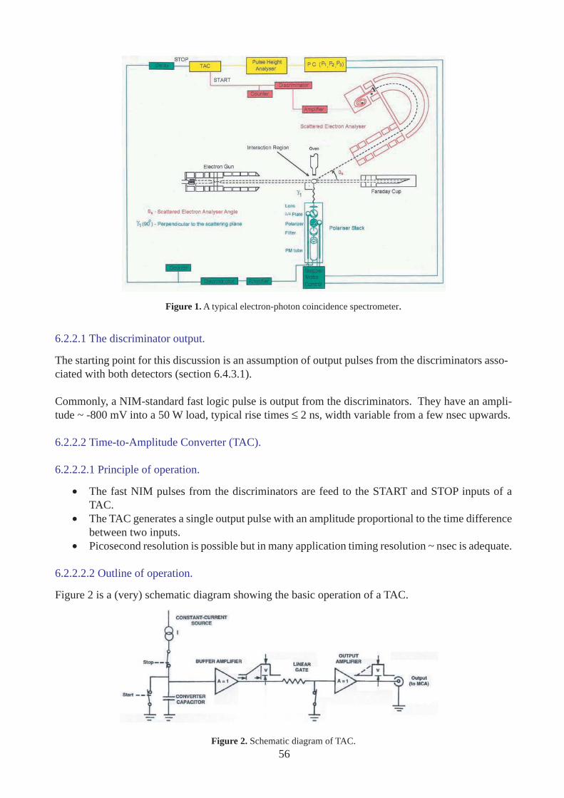
56
6.2.2.1 The discriminator output.
The starting point for this discussion is an assumption of output pulses from the discriminators asso-ciated with both detectors (section 6.4.3.1).
Commonly, a NIM-standard fast logic pulse is output from the discriminators. They have an ampli-tude ~ -800 mV into a 50 W load, typical rise times ≤ 2 ns, width variable from a few nsec upwards.
6.2.2.2 Time-to-Amplitude Converter (TAC).
6.2.2.2.1 Principle of operation.
• The fast NIM pulses from the discriminators are feed to the START and STOP inputs of aTAC.
• The TAC generates a single output pulse with an amplitude proportional to the time differencebetween two inputs.
• Picosecond resolution is possible but in many application timing resolution ~ nsec is adequate.
6.2.2.2.2 Outline of operation.
Figure 2 is a (very) schematic diagram showing the basic operation of a TAC.
Figure 1. A typical electron-photon coincidence spectrometer.
Figure 2. Schematic diagram of TAC.

57
Key steps of operation:
• The arrival of the leading edge of the START signal from one discriminator opens the elec-tronic START switch and the converter capacitor begins to charge at a rate set by the constant-current source.
• The leading edge of the STOP pulse from the second discriminator opens the STOP switch andprevents any further charging of the capacitor.
• Because the charging current I is constant, the voltage developed on the capacitor is givenby,
V = I t/C,
where t is the time interval between the start and stop pulses and C is the capacitance of theconvertercapacitor, i.e.,
PULSE HEIGHT is PROPORTIONAL to the TIME DIFFERENCE betweenSTART and STOP PULSES
• The voltage pulse is passed through the buffer amplifier to the linear gate which opens to passthe pulse through the output amplifier and TAC output.
• All switches are closed and the capacitor discharged in preparation for the nextset of START and STOP pulses.
The output pulses are rectangular, normally ranging in height from 0 – 10 Volts positiveand a few microseconds wide.
6.2.2.3 The Multi-channel Pulse Height Analyser (MCA).
A number of techniques can be used to deal with the output pulses from the TAC. The MCA is themost common and will be discussed here.
6.2.2.3.1 MCA Basics.
• The MCA consists of an analogue-to-digital converter (ADC), a histogramming memory and avisual display of the histogram recorded in the memory.
• The ADC measures the amplitude of the TAC output pulse and converts that value to a digitalnumber.
• For sequentially arriving pulses, the digital outputs from the ADC are fed to a dedicated memoryand sorted into a histogram to record the number of events counted in each pulse heightinterval.
• This histogram represents the spectrum of input pulse heights and hence the time spectrummeasured by the TAC.
Most MCA’s are now computer based, consisting of plug-in cards and associated software. A goodexample is the Ortec TRUMP-PCI Plug-in card and software (see appendix1).
NOTE: Most of the hardware and software outlined in these discussions have been developed fornuclear physics and in general contain many features with no relevance to atomic scattering studies.

58
6.2.2.4 The pulse height (time) spectrum.
Figure 3 shows a typical pulse height spectrum measured in thE laboratory in Newcastle.
Figure 3. Typical measured pulse height spectrum (scattered electron-Lyman a photon coincidence signal from excita-tion of H(2p)).
The spectrum consists of two parts:
• A ‘flat’ background (see later comment) with equal numbers of counts, within the statisticaluncertainty) in each channel. This background, often call the RANDOM coincidence signal,is due to events uncorrelated in time, for example, an electron from one collision and aphoton from a different collision arriving within the time window of the TAC. In generalthey can be due to any process where the conditions for detection in each detector are satis-fied but the events are uncorrelated.
• A narrow peak due to particles from the same collision, the TRUE signal, superimposed onthe random background. In this study no attempt has been made to optimise the timingresolution in the experiment, ~20 ns FWHM. Time spectra down to ~1 ns FWHM are read-ily obtained, higher resolutions are possible but more difficult.
Note that the position of this peak can be moved by the insertion of a delay, active orpassive, before the TAC (see figure 1).
6.2.2.4 Extraction of the coincidence signal from the pulse height spectrum.
Figure 3 also shows a simple and common way of extracting the TRUE coincidence signal of interestfrom the pulse height analyser, either manually or using appropriate software.

59
Steps involved:
• Set up two REGIONS OF INTEREST (ROI)
• one taking in the channels containing the TRUE coincidences, labelled CROI and correspond-ing to a time window ∆t
• one taking in only the background region (BROI) corresponding to a time window ∆t’.
• All MCAs will give the total coincidence counts in each ROI, Nc, the trues + randoms in CROIand Nb, the randoms in BROI.
• The number of true coincidences, NT, is then given simply by,
NT = N
c - N
b(∆t/ ∆t’)
• The statistical uncertainty in NT is given by,
∆NT = N
c + N
b(∆t/∆t’)[ 1 + (∆t/ ∆t’)]1/2
Hence it is essential that ∆t is kept as small as possible and ∆t’ large.
6.3 Points to bear in mind.
6.3.1 True and random coincidence rates.
It is important to remember the dependence of these in terms of the target density, n, and the incidentcurrent, I. If coincidences are collected over a time t, the number of true coincidences is given by,
NT = CnI t,
whereas the number of random coincidences is given by,
NR = K ∆t(nI)2t.
C and K are related to the process studied and efficiencies.
Hence the true/random ratio is given by,
NT/N
R = C/KnI ∆t
Reducing I and/or n improves the true/random ratio but it also reduces NT and therefore increases the
fractional error,
∆ ∆∆
∆N
N t nIK
t
ttT
T
c
bc= + +
⎛⎝⎜
⎞⎠⎟
⎛
⎝⎜⎞
⎠⎟⎡
⎣⎢⎢
⎤1 11
C
C
⎦⎦⎥⎥
1 2

60
6.3.1.1 Implications.
• Minimise ∆t, the coincidence window covering the true peak and maximise ∆t’, the randomswindow.
• Increase nI , but only until the second term in ∆NT/ N
T becomes dominant.
• Provided the angular resolution is still acceptable, ∆NT/N
T is improved by increasing the
angular acceptance of the detectors in C.
6.3.2 The Random background.
In this analysis a flat background due to the random coincidences has been assumed.
• This may not be true for high START and STOP input rates to the TAC.• This is because the TAC ignores all subsequent start pulses and additional stop pulses until it
has finished converting the first pair of stop and start pulses.• Hence for high random input rates the TAC will process the pulses arriving earlier in prefer-
ence to those arriving later and the measured time spectrum is distorted.
If the average random count rate R at both inputs is reduced to
R < 0.01/Trange
,
where Trange
is the time range set on the TAC, the distortion on the time spectrum will be less than 1%.
6.3.3 Coincidence resolution
In general the coincidence resolution (FWHM and assuming Gaussian profiles) is given by the inci-dent beam resolution convoluted with the resolutions of the two detector spectrometers. In the case ofan (e,2e) study this is given by,
where the subscripts, 0, 1, 2, refer to the incident and detector resolutions, respectively.
References.
1. I. E. McCarthy and E. Weigold, Phys Rep 27C, 275 (1976).2. D. V. Fursa, I. Bray, B. P. Donnelly, D. T. McLaughlin and A. Crowe, J. Phys. B 30, 3459 (1997).3. G.C. King, F. H. Read and R. E. Imhof, J. Phys. B 8, 665 (1975).4 G. C. King and A. Adams, J. Phys. B 7, 1712 (1974).5. M. Dogan and A. Crowe, J. Phys. B 35, 2773 (2002).6. R. E. Imhof, A. Adams and G. C. King, J. Phys. E 9, 138 (1976).
∆ ∆∆ ∆
E EE Ec
202
222
1
1 1
1
= + +⎛
⎝⎜
⎞
⎠⎟
−

61
7. Data and Signal AnalysisProfessor John T. Costello and Dr. Hugo de Luna
School of Physical Sciences and National Centre for Plasma Science and TechnologyDublin City University
[email protected] and [email protected]
7.0 Introduction
Contents
7a). Data analysis for a typical collision physics experiment (de Luna)
7b) Signal capture and processing applied to a fast pulse detection experiment (Costello)
7a.1) Counting rate problems in ion-atom/molecule cross section experiments
Experiments using time-of-flight (TOF) spectrometers are nowadays the core of a powerful methodologyfor the study of the basic mechanisms of ionization of atoms and molecules in the gaseous phase byphotons, electrons or neutral/charged particles. Absolute measurements of the recoil yields related tomulti-electronic transitions or molecular fragmentation induced either by electronic, photonic, or ioniccollisions are essential to the verification of the accuracy of theoretical models, to the provision ofreliable input data for computer codes designed to simulate more complex phenomena, and forquantitative analytical purposes.
In order to build up an experiment where cross sections of ion-atom/molecule reaction can be measured,there are several issues to be taken into account on the target and TOF design. If absolute measurementsare required, a gas cell design should be used in order to assure: (i) the absolute measurement of thepressure inside the gas cell, (ii) the independence of the detection efficiency on the loading gas typeand pressure, (iii) independence of the detection efficiency on the recoil ion charge state (ionizedtarget product), (iv) the quality and purity of the incident beam, and finally (v) the possibility ofmaking a second type of measurement to calibrate the detectors.
In this section we will discuss the detection limit for low cross sections reactions for a ion-atom/molecule collision (10-1 to 10-2 Mb). Consider a fast proton beam (projectile) crossing a target cellfilled with a pure gas, for example Xe, (figure 1). Following a binary collision, either, projectile andtarget can change its charge state. For simplicity lets only consider the energy range where electroncapture (charge transfer reaction) can be disregarded compared to the direct ionization.
Figure 1: Schematic set-up for a time of flight ionization experience using a gas cell target and a solid state detector(surface barrier) for the projectile collection.

62
As a concrete case, consider the experimental time-of-flight set-up of Santos et al 1(figure 2).
Figure 2: Top and side views of the chamber and gas cell. A sketch of the TOF mass spectrometer used in the presentexperiment is also represented all distances are in mm.
Under single collision condition, recoil ion production rate can be written as (see Tawara 2):
Nq+ = I0 π σq+ (1)
Where, Nq+ stands for the number of true coincident events per second, between the target recoil andthe projectile final charge state H+ (direct ionization). The incident projectile rate I0 is limited by thetype of detector used for the projectile detection. To avoid problems with detection efficiency letsconsider a solid state detector, where 100% efficiency can be assumed in the energy range of tens ofkeV to hundreds of MeV.
The target thickness π is given by:
π(P0) = 273L εεεεεleff P0 /(273+T)760 (2)
Where for the apparatus used by Santos:
L = Loschimit number of gas (2.678 X 10¹⁹ atoms/cm3)εleff = effective target length = 1.60 cm
P0 = absolute target pressure kept order of 10-3 torrT = temperature of the target gas 24 degrees centigrade
This will give a target thickness of 5.2 X 10¹³ atoms/cm2. In order to analyze the coincident rates forthis system, we have to know the values of the cross sections for direct ionization of Xenon by fastprotons. We work out the true coincidence ratio of Xe ionization, using the TOF apparatus of Santos(Fig. 2) plus a projectile detection system composed by a solid state detector (surface barrier) whichthe incident counting rate is limited to 2 X 10³ particles per second.
Nq+ = 1017 σq+, cross sections given in units of cm2 (3)

63
The direct ionization cross sections were extracted from the work of Cavalcanti et al 3 for the energyrange of 750 keV to 3.5 MeV. The coincidence ratio is shown for Xe+ Xe2+ and Xe3+ in figures 3.
Figure 3: typical true coincidence counting ratio for Xe ionization by fast protons.
As shown in figure 3, the poorest coincidence ratio is for the case of Xe3+ production at 3.5MeV =0.0034 particles per second. With this coincidence rate, it would take approximately 40 hours toaccumulate at least 500 events (2% statistical error). This would make the measurement unfeasible,since a typical MCP dark count (order of 0.05 counts per second) could give a same order falsecoincidence ratio (background). Besides, long time measurements are often affected by pressure driftand beam instability.
In order to overcome the rate problem often present in the lower cross sections reactionmeasurements, different decisions can be taken. The applicability of the solution will
depend on each individual apparatus set-up.
For this particular example we are analyzing, let look three different possibilities:
• Increase of target thickness π• Enhancement of the effective target length εl
eff
• Increase of the incident projectile rate I0
Target thickness πAlthough the increase in target thickness, by increasing the cell pressure, seems to be the straightfor-ward way to improve the coincidence counting ratio, two problems can mask the true coincidencemeasurements. First, the single collision condition could no longer be valid if terms of order π2 orhigher start to contribute to equation 1 (for more details see discussion on reference [2]). Second, gascell targets are designed in a differential pump set-up, one have to be careful when calculating thedifferential pump speed to avoid projectile charge exchange in the backpressure gas along the beamtransport line (beam contamination). In the experimental set-up illustrated here, the working pressureof 10-3 torr was chosen as the best condition to give the maximum coincidence counting rate andminimal beam contamination.
Effective target length εεεεεleff
The effective target length is a function of the MCP detection efficiency (approximately 50%) and theTOF acceptance. The acceptance of the TOF depends on the geometry and on the electric field appliedfor the recoil ion extraction. In the apparatus discussed here, εl
eff was found to be 1.6 cm. The main
geometrical limit to the effective target length is the 4 mm aperture in the drift tube, shown in figure 2.
0.5 1.0 1.5 2.0 2.5 3.0 3.510-3
10-2
10-1
100
101
Xe3+
Xe2+
Xe+
Coi
ncid
ence
Rat
e (p
artic
les/
sec)
Energy (MeV)

64
Increasing or removing the 4mm, aperture would lead to a significant increase of the effective length,since a 20mm diameter MCP is used for the recoil detection. This would, on the other hand, increasethe recoil ion charge exchanging along the drift tube, affecting drastically the cross section measure-ments.
Incident projectile rate I0
Increasing the projectile incident rate, would be a solution, if detectors able to handle a bigger count-ing rate are available. Continuous channel electron multipliers detectors (channeltrons), for example,can detect at least 10 times more particles than a solid state detector without losing efficiency. Theefficiency for those detectors is estimated to be approximately 100% for ion energies above 4 keV 4.The channeltron can be placed directly in front of the beam or a secondary electron detection arrange-ment can alternatively be used. For the secondary electron emission arrangement the detection effi-ciency is maximum (~90%) at energies between 500 and 1keV.
The solution employed by Cavalcanti was to use a sensitive position MCP. In order to avoid transitorylocal efficiency deterioration, a 600 Å thick Al diffuser was used to guarantee a broad illuminationover the whole microchannel plate sensitive area (figure 4). Using the diffuser, counting rates of 5 X10⁴ particles per second could be employed without a significant loss of the coincident signal. There-fore an experimental run that would normally take an accumulation time of 40 hours with a surfacebarrier detector was reduced to one and a half hour.
Figure 4: schematic view of the Al diffuser set-up.
References:
1. A.C.F. Santos et al. Review of Scientific Intruments 73, 2369, (2002).2. H. Tawara. Review of Modern Physics 45, 178, (1973).3. E.G. Cavalcanti et al. J Phys. B 35 3937, (2002).4. Galileo Electron-Optics Corp. Technical Notes.
slit
cleaningmagnet
analyzingmagnet
MCposition-sensitive
MCP
pusher
TOF
to pump
to pump
gas
recoil ion
coincidence
1680 V
720 V
-3640
H+
Al diffuser

65
7b.1 Signal (digital) processing and analysis
Key Text: Digital Signal Processing with Computer Applications (2nd Ed.) Paul A Lynn and
Wolfgang Fuerst, (Publisher: John Wiley & Sons, UK)
In most modern experiments analog signals are converted to digital data format andso effectively we are still talking about data analysis (but of a very specialized kind !).
So we will spend a little time reviewing:
Signal Sampling and Averaging
Sampling frequency and Shannon’s theorem
We will consider Linear Time-Invariant signals and systems only since these are what we normallydeal with provided we do not saturate our detectors. Non LTI systems (i.e., non linear and adaptivesystems are for another day, in fact days). No time to go into this either but it turns out that signalsand systems looks like one and the same thing in practical analysis. Will not consider issues aroundanalog to digital conversion – assume you have fast transient digitizer/ digital storage oscilloscope.To illustrate the ideas we will take the practical example of:
Real (optical) signal capture and analysis (From DESY FEL experiment)
We will take the case of fast (and ultrafast) photon detection with photodiodes and a streak camera(see appendices for details of detectors). Although applied to fast photon detectors, the basic princi-ples outlined can be applied to all detectors producing a fast analog signal. Doesn’t matter if theindependent variable is time as above or space (e.g., linear photodiode array readout) and can beextended to 2D to encompass image detection and processing, now becoming more frequent inatomic, molecular and optical physics experiments.
7b.2) Fundamentals Signal Sampling and Averaging
Keywords: Shannon, Sampling Theorem, Sampling Interval, Sampling Frequency, Aliasing.
In many real experimental situations we measure the response of a system to a excitation by a shortpulsed stimulus, e.g., fluorescence from an atomic or molecular beam excited by an ultrashort laserpulse. The key to such experiments is that the fluorescence signal is locked to the excitation signal,which is used as the trigger pulse to initiate the data acquisition).
PULSED LASER(Pulse Duration = 100fs – 10 ns)
Trigger
Signal Input (Ch1)
DIGITAL STORAGEOSCILLOSCOPE
Monochromator orOptical Filter
PMT
SAMPLE
Time (ns)
ZoomDelay
ZoomTimebase
V(Volts)

66
Requirements
The signal to be sampled must be repetitive (but not necessarily periodic) It must a have a time synchronized and clean trigger pulse associated with it
Terminology
Zoom Delay: Time interval from trigger pulse to first sampled point on waveform
Zoom Timebase: Time interval form first to final sampled points
Sampling interval: Time interval between successive sampled points on the waveform
Frame: A complete set of stored waveform samples
Samples per point: The number of time you sample a particular point on the waveform (used toimprove signal to noise ration – see later)
7b.3) Improving signal to noise ratio (SNR) is sampled waveform systems
Since signals are quite often buried in noise signal sampling and averaging is the preferredmethod for waveform extraction from noise.
Principle: when a noisy signal is sampled many times, the random noise componentaverages to zero while the signal component averages to its original form.
Consider a noisy signal which is sampled to make a data set of say ‘N’ points, i.e., each frame is Ndata points long. We write the value of the noisy signal in frame ‘j’ at some time point t
i as:
Now sample each point ‘M’ times or equivalently make ‘M’ frames and add them together. Theaverage value of the noisy signal at time t
i is:
s t n tj i j i( ) + ( )
For a stable signal all values, s1(t
i) = s
2(t
i) =…. s
j(t
i) =… and the signal averages to itself.
However the noise values are randomly distributed about zero and average to zero.
s t n t
Mj i j i
j
M ( ) + ( )⎡
⎣⎢
⎤
⎦⎥
=∑
1
s t
Ms t s tj i
j
M
i i
( )⎡
⎣⎢
⎤
⎦⎥ = ( ) = ( )
=∑
1
n t
Mn tj i
j
M
i
( )⎡
⎣⎢
⎤
⎦⎥ = ( ) →
=∑
1
0
To determine the signal to noise ratio (power) improvement one simply looks at the variance of thenoisy signal before and after averaging.
Variance of input signal component (1 sample) = σ si j i j is t s t2 22
0= ( ) − ( ) =
Variance of output signal (M sample average) = σ soj i j i
j
M s t s t
M2
22
1
0=( ) − ( )⎡
⎣⎢⎢
⎤
⎦⎥⎥
==∑
Variance of input noise component (1 sample) = σ ni j i j in t n t2 22
= ( ) − ( )

67
Variance of output signal (M sample average) = σ noj i j i
j
M n t n t
M2
22
1
=( ) − ( )⎡
⎣⎢⎢
⎤
⎦⎥⎥=
∑
So although n t n t andMj i j i no
ni( ) = ( ) ≠ =2
22
22
0 0, σ σ .
Hence the mean square value of the noise (i.e., the noise power) is reduced by a factor of M. Inother words:
When a noisy signal is sampled and averaged ‘M’ times the signal power to noise (SNR) ratio isincreased by a factor of M, the signal (voltage) to noise ratio by a factor of √M
7b.4) Shannon’s Sampling Theorem
Consider a sampled sinusoidal waveform which repeats each 2π radians (Fig 1). The waveform isdisplayed at 4 samples per cycle, 6 samples per cycle and 12 samples per cycle. How many samplesper cycle do actually you need before you can confirm that it’s a sine wave ?
The answer lies in Shannon’s Sampling Theorem. In this case it is ‘more than two’. The formalstatement of the theorem goes something like this –
A waveform may be reproduced from its sampled form provided that the samplingfrequency is greater than twice the highest frequency component of the waveform
So need only more than two samples per cycle to reproduce an analog signal from its constituentsamples ! Let me show you in .
X
0 2 4 6 8 10 12Sample Number
Digital Carrier (Sampling Waveform)
-1.5
-1
-0.5
0
0.5
1
1.5
0 50 100 150 200 250 300 350
Sig
nal L
evel
(m
V)
Time (ns)
2 4 6 8 10 12
-1
-0.5
0
0.5
1
Sample Number
Sampled cosine waveform (12 Samples/Cycle)

68
So we have a periodic train of sampling pulses with a repetition frequency of:
Where Ts is the so-called ‘sampling interval’. To obtain the sampled waveform we simply multiply
(modulate in the jargon) the ‘digital carrier’ by waveform (information). In frequency space we canwrite the periodic sampling waveform as (let’s assume it’s symmetric about zero time):
Multiply it by the information signal (say a cosine at frequency fm) to get:
So the sampled waveform consists of the original waveform at frequency fm plus a series of
with sidelines (bands) centred about the sampling frequency and its harmonics.
A A nf tn sn
01
2+ ( )=
∞
∑ cos π
fTs
s
= 1
A f t A A nf t
A
m n sn
1 01
1
2 2cos cosπ π( ) ⋅ + ( )⎡⎣⎢
⎤⎦⎥
=
=
∞
∑
AA f tA A
nf f t nfmn
s m0122
2 2cos cos cosπ π π( ) + +( )( ) + ss mn
f t−( )( )⎡⎣ ⎤⎦=
∞
∑1
f fs > 2 max
In the example above the ‘information signal’ is simply a single tone at a frequency fm = 1 MHz -
ironically this standard example uses the archetypal ‘no information’ signal. The sampling fre-quency is 6 MHz or 6 Samples/ Cycle.
So in order to reproduce the original cosine waveform at fm = 1MHz we simply need
to low pass filter the sampled waveform
However we have to ensure that the cutoff frequency of the filter lies between fm and f
s - f
m so that
we pass the 1 MHz signal and reject all high frequencies, i.e., in order to reproduce the originalsignal from its sampled form we require f
m < f
s - f
m or:
In practice a real signal will have contain frequencies up to some cutoff fmax
and so Shannon’stheorem generalizes to:
0
0.2
0.4
0.6
0.8
1
1.2
1.4
1.6
0 2 4 6 8 10 12 14 16
Sampled Waveform Spectrum (Sampling Frequency 6 MHz)
Am
plitu
de (
Arb
. Uni
ts)
Frequency (MHz)
fm
fs - f
mfs + f
m
2fs - f
m2f
s + f
m
GuardBand
Low PassFilter
f fs > 2 max

69
Terminology
Sampling Interval: Time between successive samples on a waveform
Sampling frequency: Reciprocal of the sampling interval
Guard band: the frequency interval between the highest frequency component on the signal to besampled and first lowest sideband.
Aliasing: Occurs when the guard band drops to zero or goes negative, i.e., when fs ≤ 2f
max
Practical points to note:
1. In general one should sample at the highest frequency (samples/cycle) possible (for signal visuali-zation) and for the longest time interval possible (longer the time window ‘T
W’over which you sam-
ple the higher the frequency resolution since the width of each feature in the signal spectrum dependson 1/T
W. Of course the limitation will be the amount of data storage you have available. In general
sampling at 5fmax is a good compromise between the Shannon baseline frequency and visualization.
2. It is important to note that a key parameter is the bandwidth of the front end amplifier of the DSOor transient digitizer used. If you sample at 1 Gsamples/sec but the DSO bandwidth is only 10 MHzthen you are oversampling by a significant amount (factor of ~50). Not quite true since a BW of 10MHz refers to the 3dB gain point and frequencies above 10 MHz will be amplified (albeit with lowergain).
3. Repetitively interleaved sampling – RIS and available on most modern digital oscilloscopes. Theidea goes as follows. Imagine a waveform frame of 1000 samples recorded at a minimum samplinginterval of 1ns. On the next trigger pulse delay the recording by 0.1 ns and record/store the wholeframe. Repeat this 9 times and interlace the sample data values. You now have effectively increasedthe sampling frequency from 1 Gsample/sec to 10 Gsamples/sec.
We should also consider impulse response and deconvolution (signal restoration) in thissection but time will not permit – defer to another day.
7b.5) Real example – detection of ultrafast pulses from the Hasylab VUV Free Electron Laserand synchronized Optical Parametric Amplifier system.
Sensitive photon detection covered earlier by Andrew. Just mention fast photodiodes here.Commercial devices are :
Thorlabs DET210 (see appendix for details)Easy to use fairly fast silicon photodiode, 200nm – 1100nm offering 1 ns risetime
Electro-Optics Technolgy ET4000 (see http://www.eotech.com/store/photodetectors.php)Fastest commercial diode available. GaAs and set for 400 – 800 nm, ~35 ps risetime
International Radiation Detectors AXUV series (see appendix for details)Very fast photodiodes, radiation hardened and sensitive from NIR to soft X-ray.AXUV-HS4. Sensitive with 200 ps risetime (we use this at Hasylab)AXUV-HS6. Not very sensitive (active area = 0.00065 mm2 !)

70
All photodiodes operated in reverse bias (photoconductive mode)
Key points (for high speed):
Use largest reverse bias possible (typically 30 – 50 V). For ns risetime standard BNCconnections/ cables suffice. For risetimes < 1 ns must use SMA cables/ connectors/
terminators.
Important to mount a capacitor (not polarized) across the power lines close to the diode resistorcombination. Effectively it acts like a rapid discharge battery and so the remote battery/ powersupply simply charges up the capacitor between optical pulses. Also, if the battery/ PSU isconnected by long leads the impedance (due to lead inductance) can be high and so limit currentflow into the photodiode
Typically C should be < 100 pF and the load resistor can be 1KΩ or so (shunted out by the 50 Ωtermination of the oscilloscope – if not terminated by 50 Ω then use an external terminator
Example from Hasylab FEL + OPA pump probe experiment –http://www-hasylab.desy.de/facility/fel/vuv/projects/pump.htm
Facility setup to carry out 2 colour experiments at high intensity on atoms and molecules. Firstexperiments in August 2005 (Orsay, DCU, QUB & DESY). Simultaneous fast IR and VUV pulsedetection needed on picosecond timescale. Could use streak camera but expensive and hard tolocate on experimental chamber permanently.
Detection of synchrotron radiation that is synchronized to FEL pulse) and fs (OPA) laser pulse onHamamatsu Streak Camera (see appendix for details)
+- C
RL To DSO
0
50
100
150
200
250
300
70 80 90 100 110 120 130 140
Dipole + OPA on Synchroscan Streak Camera
Inte
nsity
(C
ount
s)
Time (ps)
OPA o/p
Dipole Rad.

71
For ‘rough’ time delay monitoring we used AXUV Photodiodes –
Pulses recorded on LeCroy 8600 series DSO with 50 ps/point single shot sampling speed (seeappendix for details)
Possible to achieve ~150 ps FWHM with ET4000 and ca. 350 ps with HS4.
Possible to measure pulse separation on timescale of 100 ps also.
AXUVHS4 - 200 psecrisetime
Basic back bias circuit
-0.01
0
0.01
0.02
0.03
0.04
0.05
0.06
2000 4000 6000 8000 1 104 1.2 104
FEL Laser Pulse (31.5 nm, 30 fs) and OPA pulse (800 nm, 100 fs)detection on AXUV HS4 photodiode (single shot)
V (
mV
)
Time (ps)
FELPulse31.5 nm/30 fs
OPAPulse100 fs/800 nm
2 x OPA800 nm/Pulses

Appendix 1. Data Sheets for various components listed in Section 3.

3-18
The Kimball Physics Tungsten Filament is a hairpin style thermionicemitter. This refractory metal filament is quite sturdy and providesstable and uniform electron emission, primarily used in scanningelectron microscopy. The standard model ES-020 consists of a0.005 inch (0.13 mm) diameter tungsten-3%-rhenium heater wiremounted on a standard glass AEI base. Custom tungsten filamentcathodes in a variety of filament sizes and configurations and a varietyof glass or ceramic AEI bases are available. Some combinations ofvarious options may not be possible due to design considerations. Alltungsten cathodes are shipped pre-fired, vacuum clean, and ready toinstall. The standard model ES-020 is usually shipped in packages often filaments, on glass AEI bases.
ELE
CT
RO
NG
UN
SIO
NG
UN
SE
MIT
TE
RS
DE
TE
CT
OR
SC
OM
PO
NE
NT
SIN
DE
X/
INF
OR
MA
TIO
N
Toll Free: 1 888 KIM-PHYS (1 888 546-7497) e-mail: [email protected]. 1 603 878-1616 Fax: 1 603 878-3700
The Ta disc cathodes, ThO2-Ir cathodes, BaO cathodes, andTungsten filaments are quite sturdy; they will survive shipping whilein the original container, and will remain stable under use invacuum; however, cathodes/filaments are easily damaged if struckor dropped. Please handle with care during installation.
The most critical parameters in the setting up of a triode gun are:1) height setting of the cathode (or filament) with respect to the
front face of the Wehnelt aperture, and 2) the axial alignment of thecathode/filament tip within the Wehnelt aperture. Heightadjustment is best done using a metallurgical microscope with afocus knob calibrated in micrometers.
Technical Notes for All Refractory Metal and Coated Thermionic Emitters:
Kimball Physics cathodes/filaments are shipped pre-fired andvacuum clean. When handling cathodes (or any surface intendedfor vacuum), the use of clean-room gloves is recommended to keepsurfaces free of fingerprints and other contaminants.Cathodes/filaments should not be exposed to mechanical orthermal shock which can damage the emission surface. It issuggested (but not required) that cathodes be brought up totemperature using a 30 or 60 second time frame; longer lifetimesmay result. It is desirable to wait a few minutes for thecathode/filament to cool down prior to venting the vacuum system.This latter procedure will help reduce oxidation in the gun structure,particularly if the cathode/filament has been run very hot.
TUNGSTEN FILAMENTSHAIRPIN THERMIONIC EMITTERS
FEATURES / OPTIONSHIGH QUALITY / PRECISION ALIGNEDFULLY ANNEALED / STRAIN FREEEXCEPTIONAL STABILITYSPECIAL WIRE / SHOCK RESISTANTPRE-FIRED / INSPECTEDINTERNATIONAL STANDARD AEI BASENON-STANDARD MOUNTING AVAILABLENEW PACKAGING / INDIVIDUALLY SECURED
ES-020 Tungsten (W) Filament
Tungsten (W) Filament Cathode mounted on standard AEI glass base (4 X)
ES-020 Tungsten Filament mounted on standard AEI glass base(other filament sizes and AEI base styles available)
ALL DIMENSIONS ARE IN INCHES(MILLIMETERS IN PARENTHESES)
2.0 X MANY OTHER FILAMENT / BASE STYLES AVAILABLE,
ESPECIALLY FOR USE IN SEM AND TEM
For retail sales in North America, see our distributor:BARRY SCIENTIFIC, INC.P. O. Box 173, Fiskdale, MA 01518TEL (800) 348-2257, FAX (508) 347-8280
FILAMENT MATERIALDISC SIZEFILAMENT WIRE SIZEHEIGHT ABOVE BASEEMITTING TIP SIZEEMISSION AREAEMISSION CURRENTHEATING CURRENTPOWER SUPPLYCAPABILITY
CATHODE LOADING
WORK FUNCTIONOPERATING TEMPENERGY SPREADLIFETIMEVACUUM LEVEL
Tungsten, 3% RheniumNone, Filament only0.005 in dia. (0.13 mm dia.)0.256 in (6.5 mm)Elliptical: 50 by 100 µm 5 x10⁻⁵ cm2
500 µA typical2.5 A to 2.8 AVoltage regulated power supply recommended, 2 V, 3 A1.0 A/cm2 recommended, typical;High loadings result in reduced lifetime.4.5 eV2500 K typicalapprox. 0.7 eVOne hundred hours at medium currents10-5 torr or better, recommended
ES-020

FEATURES / OPTIONS:EXTENDED LIFETIME
GUARANTEED LIFETIME
THOUSANDS of HOURS IN CLEAN VACUUM
(MEASURED IN SURFACE LOSS)
GUARANTEED AGAINST MOUNTING
STRUCTURE FAILURE
EXCEPTIONAL STABILITY
THERMAL / CHEMICAL / MECHANICAL / ELECTRICAL
PRECISION MACHINED CARBON MOUNTING
HIGH OVER-TEMPERATURE TOLERANCE
HIGH BRIGHTNESS / LOW ENERGY SPREAD
<100> ORIENTED SINGLE-CRYSTAL
BEST QUALITY / HIGH PURITY MATERIAL
ACCURATE MICROFLATS
SUPERIOR OPTICS / CONTROLLED SOURCE SIZE
STANDARD DIAMETERS AVAILABLE
3-2Toll Free: 1 888 KIM-PHYS (1 888 546-7497) e-mail: [email protected]
Tel. 1 603 878-1616 Fax: 1 603 878-3700
HEATING CURRENT FLOW
LaB6 CATHODESSINGLE-CRYSTAL LANTHANUM HEXABORIDE
ELE
CT
RO
NG
UN
SIO
NG
UN
SE
MIT
TE
RS
DE
TE
CT
OR
SC
OM
PO
NE
NT
SIN
DE
X/
INF
OR
MA
TIO
N
LaB6 crystal mounted on carbon heater rod, and heldin place by precision carbon ferrule; note roundnessand smoothness of microflat.
FOR USE IN:SCANNING ELECTRON MICROSCOPES
TRANSMISSION ELECTRON MICROSCOPES
ELECTRON LITHOGRAPHY SYSTEMS
ELECTRON ACCELERATORS
X-RAY SOURCES
FREE ELECTRON LASERS
CUSTOM APPLICATIONS
ES-423E (Extended Life) LaB6 Crystal
LaB6 single crystal cathode mounting (10 X)Heating current path through precision-machined, single-piece carbon rodand mounting strips; sub-base provides rigidity and easier mounting.
The Kimball Physics ES-423E (Extended Life) Lanthanum Hexaboride
Cathode is a high performance, resistively heated, thermionic electron
source. It is currently employed in many brightness-limited electron
optical systems: SEM’s, TEM’s, probes, electron lithography systems,
etc. It is based on a well-proven heater structure, which has recently
been further refined with features that include improved reliability of the
heater circuit, improved stability of the LaB6 crystal, and less exposure
of LaB6 to reduce Wehnelt aperture contamination. Lifetimes in excess
of 6 months of continuous operation are regularly achieved in
commercial SEM’s and TEM’s with suitable gun vacuum. Continuous
operation at the full operating temperature improves the thermal
stability of the gun and hence beam current stability. It is no longer
necessary to wait hours for stable beam conditions in order to perform
quantitative EEL or EDX measurements.
The emitter is a 15 µm-diameter (standard), <100> oriented-single-
crystal, surface (standard), mounted on the end of a single-piece,
stress-free, carbon heater rod, held in place by a carbon ferrule. The
rod has been precision machined with a 100 µm slot cut along the axis,
such that the heating current goes up one side and down the other.
The small area of the heating current loop keeps the unwanted heater-
current magnetic field low. Because the rod is one single piece, no
heating current passes through the crystal; there are no high-
temperature current-carrying joints. A high degree of axial symmetry
keeps mechanical motions small. The small physical size fits most
Wehnelts with ease. In the ES-423E, the crystal can be completely
evaporated away without affecting the heating circuit. The very tight
tolerances, and the enclosed structure prevent the loss of LaB6 in the
mounting region throughout the entire crystal life. Reduced material
loss also means less Wehnelt contamination. Emitter dimensions are
machined to a 2 µm tolerance, (standard, 2 µm to 16 µm for microflats
up to 320 µm) with a tilt tolerance of 0.5o. Microflat alignment to the
instrument base can be provided to a tolerance of 13 µm for x, y and
76 µm for z, the height above the base (less than 70 µm on request).
A high angular tolerance is maintained on the perpendicularity of the
oriented single-crystal emission plane to the electron optical axis. All
cathodes receive a stabilizing run-up prior to shipment.
With electron-gun oxidizing-gas partial pressures kept below 10-7 torr,
many instruments can achieve thousands of hours of stable cathode
operation. In SEM type instruments, lifetimes up to 3000 to 4000 hours
may be achieved at operating temperatures of 1850 K (corresponding
to material surface loss rates in the 0.025 micron/hour range), with full
brightness and excellent stability. With somewhat reduced
brightnesses, as required by typical TEM instruments, lifetimes can be
even longer. The ES-423E mounting structure will last more than
10,000 hours. Moreover, neither the electrical heating circuit drive
impedance nor the thermal properties will drift perceptibly over that
period. Chemical reactivity and mechanical drift problems have been
eliminated.
LaB6 SINGLE CRYSTAL
CARBON HEATER ROD
CERAMIC
SUB-BASE
CARBON FERRULE
MOUNTING
STRIP
BASE
PRECISION MICROFLAT
ON LaB6 CRYSTAL
BASE PIN

3-3
LaB6 CATHODES
It is not necessarily possible to achieve all maximum specificationssimultaneously. Specifications Subject to Change Without Notice.
The real figure of merit of a thermionic electron emitter is the number
of coulombs of electrons which may be boiled off per kilogram of
cathode surface evaporated away. LaB6 is an order of magnitude
superior to the refractory metals in this key parameter. Any failure of a
cathode mounting structure, before the LaB6 cathode itself has been
used up, represents a waste of cathode life. The ES-423E single-piece
stress-free ultra-stable carbon mount is unique. Unlike other designs
which operate near the temperatures where chemical instabilities will
set in, the ES-423E carbon mount is almost impossible to destroy by
accidental over-temperature. The melting point of Lanthanum
Hexaboride itself is somewhat over 2800 K; there have been examples
of crystals being melted (extreme over-temperature), in which the
ES-423E carbon mount survived. The Kimball Physics mount is
guaranteed.
ES-423E Single cone-shaped crystal LaB6 cathode mounted on an AEI Base
Heater Voltage and Current vs Temperature; ElectricalCharacteristics vary only a few percent from Cathodeto Cathode, thus insuring predictable operation.
ALL DIMENSIONS ARE IN INCHES
(MILLIMETERS IN PARENTHESES)
The ability to run over-temperature may also be utilized to clean a
contaminated crystal, and reduces the risks associated with less
experienced operating personnel.
This small source size fits most Wehnelts with ease. In excellent
vacuum with low material loss rates, the size of the cathode does not
limit lifetimes. The Kimball Physics ES-423E Long Life Lanthanum
Hexaboride Cathode is the most recent improved version of the IR 100
Award Winning design which has been used in many instruments types
for many years. Kimball Physics invented the Directly Replaceable
Lanthanum Hexaboride Cathode. Take advantage of the most
experience in the business.
ES-423 LaB6 Cathode (single cone-shaped crystal with microflat emitting surface)
mounted on standard AEI base (4 X)
2.0 X
ES-423 LaB6 Cathode (single cone-shaped crystal with microflat emitting surface)
mounted on a Kimball Physics CB-104 ceramic base (4 X)
ES-423E Single cone-shaped crystal LaB6 cathode mounted on a CB-104 ceramic base
2.0 X

LaB6 CATHODES
ELE
CT
RO
NG
UN
SIO
NG
UN
SE
MIT
TE
RS
DE
TE
CT
OR
SC
OM
PO
NE
NT
SIN
DE
X/
INF
OR
MA
TIO
N
3-4Toll Free: 1 888 KIM-PHYS (1 888 546-7497) e-mail: [email protected]
Tel. 1 603 878-1616 Fax: 1 603 878-3700
For more information on LaB6 operation in TEM’s and SEM’s you may download detailed technical bulletins from the website cathode support page.
# LaB6-01 General Guidelines for Operating LaB6 Cathodes.
# LaB6-02 The Relationship Between LaB6 and Cathode Life and Gun Vacuum
# LaB6-03 Emission Drift—LaB6 and Gun Stability.
# LaB6-04 Oxygen Activation of LaB6 Cathodes—The Double Saturation Effect
# LaB6-05 Kimball Physics ES-423E LaB6 Cathode Style 60-06 (60° Included Cone Angle, 6µm Diameter Flat)
# LaB6-06 Kimball Physics ES-423E LaB6 Cathode Operating Instructions for LEICA/Cambridge Stereoscan Series SEM’s
# LaB6-07 Recovery of Emission From ES-423E LaB6 Cathodes Following a Vacuum Dump
TRUE TEMPERATURE vs HEATING CURRENT
(AVERAGE)
HEATING CURRENT (A)
0.0 0.5 1.0 1.5 2.0
TR
UE
TE
MP
ER
AT
UR
E(K
)
1000
1200
1400
1600
1800
2000
ES423_Temp-I_00.eps
ES_423_catalog_J12300124graphs.jnb
Using Equations for Fit
LANTHANUM HEXABORIDE CATHODEMODEL# ES-423E02/20/01
BASE STYLE: AEI
LaB6
CRYSTAL SHAPE: 90o
CONE
(AVERAGE OF 15 CATHODES)
EMISSION CURRENT vs HEATING CURRENT
HEATING CURRENT (A)
0.0 0.5 1.0 1.5 2.0
EM
ISS
ION
CU
RR
EN
T(A
)
10-10
10-9
10-8
10-7
10-6
10-5
10-4
10-3
10-2
ES423_Emis-I_00.eps
ES_423_catalog_J12300124graphs.jnb
Using Equations for Fit
0.200 mm DIA.
0.100 mm DIA.
0.040 mm DIA
LANTHANUM HEXABORIDE CATHODEMODEL# ES-423E02/20/01
BASE STYLE: AEI
LaB6
CRYSTAL SHAPE: 90o
CONE
CALCULATED EMISSION CURRENTFOUR SIZES OF MICROFLATON LaB6 CRYSTAL:
0.015 mm DIA.
V-I CHARACTERISTIC (AVERAGE)
HEATING CURRENT (A)
0.0 0.5 1.0 1.5 2.0
HE
AT
ING
VO
LTA
GE
(V)
0.0
0.5
1.0
1.5
2.0
2.5
3.0
3.5
ES423_V-I_00.eps
ES_423_catalog_J12300124graphs.jnb
Using Equations for Fit
LANTHANUM HEXABORIDE CATHODEMODEL# ES-423E02/20/01
BASE STYLE: AEI
LaB6
CRYSTAL SHAPE: 90o
CONE
(AVERAGE OF 15 CATHODES)
Typical performance;data for guidance only.
CATHODE MATERIAL
CATHODE SHAPE
MICROFLAT SIZE
HEATER
EMISSION AREA
HEATING CURRENT
CATHODE LOADING
WORK FUNCTION
OPERATING TEMP
ENERGY SPREAD
LIFETIME
VACUUM LEVEL
POWER SUPPLYCAPABILITY
Lanthanum Hexaboride (LaB6) single crystal
Cone with 90o sides and microflat tip
Standard: 0.015 mm dia., larger or smalleravailable
Single piece carbon rod
1.7x10⁻⁶ cm2 standard microflat, excluding sides
1.7A to 2.1A
20-30A/cm2 recommendedHigh loadings result in reduced lifetime
2.69 eV
approx. 1700-1900K
approx. 0.4 eV
Thousand plus hours with medium currents, goodvacuum
10-7 torr or better, recommended
Voltage regulated power supply recommended, 4 V, 3 A
ES-423E
Standard microscopy styles include: 90-15, 90-20, 60-06
A second requirement is that it must be possible to
accurately and correctly position the cathode behind the
Wehnelt. Some guns do not have adequate adjustment
systems. Another requirement is for controllable bias
resistors, which can reach adequately high values; some
instruments are limited by values which are too low. While
not a requirement, it is desirable to have the capability for
independent bias. It is also desirable to have accurate
heater circuit voltage and current meters. Most of these
problems can be solved in most instruments, however
significant efforts may be required. Note that the higher the
brightness level desired, the lower the tolerance to tip
recession. The electron optically allowed tip recession,
and the acceptable contamination on the Wehnelt (before
gun instabilities set in), are in fact the life-limiting
parameters for current state-of-the-art cathodes. More
information on all these topics may be found in the Kimball
Physics Technical Bulletins.
Instrument Conditions for LaB6 Cathodes
While the cathodes can be fitted to virtually any instrument,
there are several requirements needed for achieving
quality results. The most important requirement is for
clean vacuum, with partial pressures of oxidizing gases
being kept below 10-7 torr in the electron gun. Many
instruments achieve adequate vacuums as a matter of
course; however many others do not. A major problem is
instruments in which the pressure measurement takes
place outside the gun itself (as in the measurement of an
ion pump current). The actual pressure inside the gun,
where outgassing is frequently high, may be much worse
than the operator is led to believe. The condition of the
cathode itself, along with that of the Wehnelt aperture, may
often be used to verify the partial pressures in the gun. It
is a waste of money to put good cathodes into poor
vacuum.

Appendix 2. Data Sheets for various components listed in Section 5.

FEATURES
* Unexcelled Timing Characteristics* 100 MHz Operation* Small Rugged Enclosure* Fast Veto For Inhibiting
DESCRIPTION
The Model 6915 is a high performance, single channel constant-fraction timing discriminator.Its small rugged packaging makes it ideal for mounting nearby the detector often in remotelocations.
Typical time walk plus input slewing of ±75pSec is achieved for inputs from threshold to 100times threshold. The threshold is adjustable from --25mV to --1Volt, and its setting is easilymonitored from a front panel test point that provides a DC voltage equal to the actual thresholdsetting.
A shaping delay cable is required to form the constant fraction pulse. The shaping delaycircuit is made complete by connecting the appropriate cable length between two delayconnectors, allowing the user to optimize time resolution by easily matching the characteristicsof the detector. A monitor output is also provided to observe the constant-fraction shaped pulseto verify that the delay cable is correct.
A fast veto input has been included to perform an anti-coincidence function. This is helpful forrejection of unwanted events early in the system. Unlike a simple gating function, it provides away of inhibiting the discriminator without adversely affecting the timing characteristics for thecurrent event being processed.
The outputs of the 6915 are non-updating and adjustable in width from 5nSec to 250nSecproviding four individually driven, current switched outputs. They are configured as two normalNIM outputs, one complemented NIM output and one positive TTL output. They have typicalrisetimes and falltimes of 1.2nSec helping to preserve the excellent timing characteristics. Theoutput transition times and pulse shapes are unaffected by the loading of the outputs in anycombination.
Phillips Scientific "A THEORY DEVELOPMENT COMPANY"31 Industrial Ave. * Mahwah, NJ 07430 * (201) 934-8015 * Fax (201) 934-8269
PhillipsPhillipsScientificScientific
MODELMODEL
69156915CF TimingCF Timing
DiscriminatorDiscriminator

INPUT CHARACTERISTICS OUTPUT CHARACTERISTICSGeneral :One input connector; 50 ohms ±2%, directcoupled; less than 5% input reflection for a 2nSecinput risetime; input protection clamps at +.7Vand - 6V and can withstand ±2 Amps (±1OO Volts)for a duration of 1µSec with no damage to theinput.
Threshold :Continuously variable from --25mV to --1Volt,15-turn screwdriver adjustment; better than±0.20%/ oC stability; A front panel test pointprovides a DC voltage equal to the actualthreshold setting.
Fast Veto :One input connector, accepts normal NIM levelpulse (-500mV), 50 ohms direct coupled; mustoverlap the negative going edge of the input pulseplus the shaping delay time to inhibit; accepts a5nSec minimum input width.
General :Four (4) output connectors; Two normal NIM leveloutputs, one complemented NIM level, and onepositive TTL output. The normal NIM outputsdeliver pulses of -16mA (-800mV across 50ohms). The complement output is quiescently-16mA (-800mV) and goes to 0mA (O Volt), duringoutput. The positive TTL output has an internalpull-up resistor of 82 ohms and will provide +2Volts across a 50 ohm load or +3.5 Volts across a1K ohm load. Output risetimes and falltimes areless than 1.5nSec from 10% to 90% levels.
CF Monitor :One output connector, drives 50 ohm load;permits observation of the shaped constantfraction pulse to verify the shaping delay isoptimized for the input pulse.
Width Control :One 15-turn screwdriver adjustment; output widthis continuously variable from 5nSec to 250nSec;better than ±0.20%/ oC stability. Non-updatingoutput regeneration will ignore any new inputswhile the output is active.
GENERAL PERFORMANCE
Shaping Delay:Requires a 50 ohm coaxial cable; recommended delay range of 500pSec to 100nSec; themaximum delay is limited only by the cable attenuation, a factor of two attenuation can betolerated without significant degradation of the time resolution; stability is better than10pSec/ C. The shaping delay time should approximately equal the input risetime plus500 pSec.
Continuous Repetition Rate:Greater than 100 MHz, with output width set at minimum, (1nSec shaping delay).
Pulse Pair Resolution:Better than 10nSec, with output width set at minimum, (1nSec shaping delay cable).
Input to Output Delay:Less than 10nSec, (with 1nSec shaping delay cable).
Multiple Pulsing:One and only one output pulse regardless of input pulse amplitude or duration.
Power Supply +8 Volts to +16 Volts @ 100mA.Requirements: --8 Volts to --16 Volts @ 225mA. An 18 inch three-wire cable is provided unless otherwise specified. Note: Since the power supplies are internally regulated, the voltages do not need to be balanced.Operating Temperature:
O C to 70 C ambient.Packaging:
Black anodized aluminum enclosure; 2.25" x 6" x 1.75", (5.72cm x 15.25cm x 4.45cm).Quality Control:
Standard 36 hour cycled burn-in with switched power cycles.4/97
Phillips Scientific "A THEORY DEVELOPMENT COMPANY"31 Industrial Ave. * Mahwah, NJ 07430 * (201) 934-8015 * Fax (201) 934-8269

The ORTEC Model 579 wideband Fast-Filter Amplifier with gated baselinerestorer (Fig. 1) enhances fast-timingmeasurements by improving the noise-to-slope ratio and providing ultra-high countrate spectroscopy capability.
A fast rise time (<8 ns), high output drive(±5 V into 50 Ω), and wide voltage gainrange (X0.9–X500) make the Model 579useful for many timing applications,including those utilizing low-gainphotomultiplier tubes. The Model 579 isparticularly suited for use with ORTECConstant-Fraction Discriminators such asModels 583, 935, or 473A in timingapplications with high-purity germanium(HPGe) or silicon charged-particledetectors (Figs. 2 and 9 and Tables 1and 2). Excellent dc and gain stability(±50 µV/°C and ±0.05%/°C, respectively)eliminate the need for a dc leveladjustment. A Busy LED and BusyOutput are included to aid in BLRadjustment and system interfacing.
In addition, the wideband gated baselinerestorer and pole-zero cancellationnetwork permit ultra-high output countingrates. A wide variety of pulse filtering isavailable for improved signal processing.The Model 579 combines continuouslyvariable gain, independently selectableintegration and differentiation timeconstants (Out, 10, 20, 50, 100, 200, and500 ns), and cable clipping capability(external cable delay), making thisversatile unit an important asset forsophisticated time and energyspectroscopy.
579Fast-Filter Amplifier
ORTEC
• For fast timing with germanium and other semiconductor detectors
• Fast <8-ns rise time
• Independent integration and differentiation
• Gated baseline restorer
• Pole-zero cancellation
• 50-Ω delay cable clipping
• Voltage gain X0.9 to X500
• Output drives to ±5 V on a 50-Ω load
®
Fig. 1. Block Diagram of the Model 579 Fast-Filter Amplifier.

Fig. 3. Model 579 Output Signals for τD = Out andτi = Out, 10, 20, 50, 100, 200, and 500 ns.
Fig. 4. Model 579 Output Signals for τi = Out and τD = Out, 10, 20, 50, 100, 200, and 500 ns.
Fig. 6. Model 579 Output Signals for τi = τD = Out at1, 2, and 5 V.
Fig. 2. Timing Resolution FWHM and FW.1M as a Function of Energy an Energy
Window of ±50 keV.
Fig. 5. Example of Model 579 Ultra-High Output Count RateCapability. Input Signal from a BNC Random Pulse
Generator at Approximately 1 Million Counts per Second.Fast-Filter Amplifier τi = τD = 500 ns.

SpecificationsPERFORMANCEINPUT SIGNAL AMPLITUDE RANGE±1 V ac, ±5 V ac with X5 internal attenuator;±35 V dc; input impedance 100 Ω, ac-coupled;50 Ω optional.
OUTPUT AMPLITUDE RANGE 0 to ±5 Vlinear into a 50-Ω load.
RISE TIME <8 ns with Integrate andDifferentiate Out, or ≅2.2 τi for other integratesettings and Differentiate Out.
OVERSHOOT <10% with Integrate Out, or<2% for any selected integration.
NOISE For maximum gain, rms noise referredto the input is <10 µV (typically 5 µV), with τi = τD = 200 ns, measured with an HP3400Atrue rms voltmeter. Wideband (200 MHz) noisefor τi = τD = Out is <50 µV (typically 40 µV).
INTEGRAL NONLINEARITY <±1% (typically0.5%) over ±5 V range into 50-Ω load.
TEMPERATURE INSTABILITYDC Level <±50 µV/°C referred to the output;factory-set within ±5 mV.Gain <±0.05%/°C.
OPERATING TEMPERATURE RANGE0 to 50°C.
CONTROLSCOARSE GAIN Front-panel 6-position switchto select X15, X25, X50, X125, X250, andX500 gain factor. When internal X5 attenuatoris used, the coarse gain factors represent X3,X5, X10, X25, X50, and X100, respectively. Acontinuously variable voltage gain of X0.9 toX500 can be obtained. (Gain reduced byfactor of two when cable clip is used.)
FINE GAIN Front-panel single-turn potenti-ometer, continuously adjustable from 0.3 to1.0.
P/Z Front-panel screwdriver adjustable potentiometer to adjust pole-zero cancellationfor decay time constants from 25 µs to ∞.
DIFF Front-panel 7-position switch selects adifferentiation time constant to control thedecay time of the pulse. Decay time ≅2.2 τDwith τi = Out. The τD settings include Out, 10,20, 50, 100, 200, and 500 ns.
INT Front-panel 7-position switch selects anintegration time constant to control the risetime of the output pulse. The rise time is≅2.2 τi with τD = Out. The τi settings includeOut, 10, 20, 50, 100, 200, and 500 ns. Risetime in the Out position is <5 ns, equivalent toa τi <2.3 ns.
INV/NONINV Front-panel locking toggleswitch selects inversion or noninversion of theinput signal.
BLR ADJ Front-panel screwdriver adjustmentto set the Gated BLR threshold from ±50 mVto ±500 mV referred to the output.
BLR GATED/UNGATED Printed wiring board(PWB) jumper selects gated or ungated BLRoperation. Factory-set in gated position.
BLR LED This feature enables the user toquickly adjust the BLR threshold setting nearthe noise peak. Front-panel LED indicates anoutput amplitude has exceeded the BLRthreshold. The BLR LED can be used as avisual indicator of the output counting rate.
COUNT RATEHigh/Low PCB jumper selects minimum BLRdead time of typically 400 ns in high positionand typically 1 µs in low position. Factory-setin low position.
ATTENUATOR PWB jumper select to passwith unity Gain or Attenuate by a factor of 5.Jumper select B to C and A to F will pass withunity Gain. Jumper select C to D and E to Fwill attenuate by a factor of 5. Factory-set atunity Gain.
INPUTSINPUT Front-panel BNC accepts input signalsof either polarity. ±1.0 V ac or ±5.0 V ac withX5 attenuator. Maximum dc voltage ±35 V.Input impedance 100 Ω (to matchpreamplifiers), ac-coupled.
CLIP Two front-panel BNC connectors toprovide delay line clipping of the input pulse.Cable impedance must be 50 Ω. Delay lineclip is 2X the cable propagation delay. Gain isreduced by factor of 2 when using cable clip.
OUTPUTSOUTPUT Front-panel BNC connectorfurnishes the amplified and shaped signalthrough Zo <1 Ω. Amplitude 0 to ±5 V into50 Ω; rise time and decay time constantscontrolled by the integrate and differentiatefilter settings.
BUSY Rear-panel BNC furnishes NIM-standard positive logic signal during the BLRbusy time.
PREAMP POWER Rear-panel standardORTEC power connector, Amphenol type 17-80090-15.
ELECTRICAL AND MECHANICALPOWER REQUIRED +24 V, 80 mA; –24 V, 80 mA; +12 V, 160 mA; –12 V, 140 mA.
WEIGHTNet 1.5 kg (3.3 lb).Shipping 3.1 kg (7.0 lb).
DIMENSIONS Standard single-width NIMmodule 3.43 X 22.13 cm (1.35 X 8.714 in.) per DOE/ER-0457T.
Ordering InformationTo order, specify:
Model Description
579 Fast-Filter Amplifier
579Fast-Filter Amplifier

FEATURES
* Guaranteed 300 MHz Operation
* Deadtimeless Updating Outputs
* Fast Veto Inhibiting
* High Fan-Out Capability
DESCRIPTION
Utilizing the most advanced technology, the Model 6904 Discriminator boasts a 300 MHz
continuous repetition rate capability. The updating feature ensures deadtimeless operation for
coincidence applications, while the double-pulse resolution is a remarkable 3.3nSec for counting
applications. A fifteen-turn potentiometer provides continuous output width adjustment from
2nSec to over 50nSec.
The threshold is variable from --10 mV to --1 Volt with a fifteen-turn potentiometer. The
threshold setting is easily determined from a test point that provides a DC voltage equal to the
actual threshold setting.
Inhibiting of the discriminator is accomplished by a Veto input which accepts a NIM level
pulse for fast vetoing. The fast veto is capable of inhibiting a single pulse from a 300 MHz input
pulse train.
The outputs are the current source type with two pairs of negative bridged outputs and two
complements. When only one output of a bridged pair is used, a double-amplitude NIM pulse
(-32mA) is generated for driving long cables with narrow pulse widths. The outputs have transition
times of less than 1.5nSec, and their shapes are virtually unaffected by loading the outputs in
any combination.
PhillipsPhillipsScientificScientific
MODELMODEL
69046904300 MHz300 MHz
DiscriminatorDiscriminator
Phillips Scientific"A THEORY DEVELOPMENT COMPANY"
31 Industrial Ave. * Mahwah, NJ 07430 * (201) 934-8015 * Fax (201) 934-8269

INPUT CHARACTERISTICS OUTPUT CHARACTERISTICS
General :
One input connector; 50 ohm –2%, direct coupled;
less than 5% input reflection for 2.0nSec input
risetime; Input protection clamps at +.7V and -5V
and can withstand –2 amps (–100V) for the
duration of 1mSec with no damage to the input.
Threshold :Continuously variable from -10mV to -1 Volt, 15-turn
screwdriver adjustment, better than 0.20%/
o
C
stability. A front panel test point provides a DC
voltage equal to the actual threshold setting.
Fast Veto :One input connector accepts normal NIM level
pulse (-500mV), 50 ohms direct coupled; must
precede the negative edge of input pulse by 3nSec,
capable of gating a single pulse from a 300 MHz
continuous pulse train.
GENERAL PERFORMANCE
General :Six (6) output connectors; two pairs of negative
bridged outputs and two complements. The bridged
outputs are quiescently 0mA and -32mA during
output (-1.6 V into 50 ohm or -.8 V into 25 ohms).
The complementary outputs are quiescently -16mA
going to 0mA during output. Output risetimes and
falltimes are typically 1.1nSec from 10% to 90%
levels. The output shapes are optimized when the
bridged outputs are 50 ohm terminated.
Width Control :One control; 15-turn screwdriver adjustment;
outputs continuously variable from 2nSec to
50nSec. Width stability is better than 0.10%/
o
C of
setting.
Updating Operation :The output pulse will be extended if a new input
pulse occurs while the output is active. A 100% duty
cycle can be achieved.
Continuous Rate :Greater than 300 MHz, 3db bandwidth and a throughput counting rate of 300 MHz with output
width set at minimum.
Pulse-Pair Resolution :Better than 3.3nSec, with output width set at minimum.
Input to Output Delay :Less than 8.0nSec.
Multiple Pulsing :No multiple pulsing, one and only one output pulse regardless of input pulse amplitude or
duration.
Power Supply Requirements :
+8 Volts to +16 Volts @ 55mA Note: Since the power supplies are internally regulated,
--8 Volts to --16 Volts @ 250mA they may be unbalanced.
Operating Temperature :0
o
C to 70
o
C ambient.
Packaging :Black anodized aluminum enclosure: 2.25" x 6.0" x 1.75" (5.72 cm x 15.25 x 4.45 cm).
Connector Type :BNC Female, LEMO and SMA female are also available, specify when ordering.
Quality Control :Standard 36-hour cycled burn-in with switched power cycles.
Options :Call Phillips Scientific to find out about available options.
4/97
Phillips Scientific"A THEORY DEVELOPMENT COMPANY"
31 Industrial Ave. * Mahwah, NJ 07430 * (201) 934-8015 * Fax (201) 934-8269

ORTEC®
935Quad 200-MHz Constant-Fraction Discriminator
The Model 935 Quad 200-MHzConstant-Fraction Discriminatorincorporates four separate andindependently adjustable timingdiscriminators in a single-width NIMmodule. Except where indicatedotherwise, the descriptions andspecifications apply to each of thefour channels in the module.
The ability of the Model 935 toprovide constant-fraction timing onfast, negative-polarity signals asnarrow as 1 ns (FWHM) makes itideal for use with microchannelplates, fast photomultiplier tubes, fastscintillators, and fast silicondetectors. The exceptionally low walkdelivered by the Model 935 is vital inachieving the excellent timeresolution inherent in these fastdetectors over a wide dynamic rangeof pulse amplitudes. The Model 935can also be used with scintillatorssuch as NaI(Tl) which have longdecay times. To prevent multipletriggering on the long decay times,the width of the blocking output canbe adjusted up to 1 µs in duration.
The Model 935 uses the constant-fraction timing technique to select atiming point on each input pulse thatis independent of pulse amplitude.When properly adjusted, thegeneration of the output logic pulsecorresponds to the point on theleading edge of the input pulse
where the input pulse has risen to20% of its maximum amplitude. Toachieve this constant-fractiontriggering, the input pulse is invertedand delayed. The delay time isselected by an external delay cable(DLY) to be equal to the time takenfor the input pulse to rise from 20%of maximum amplitude to maximumamplitude. Simultaneously, theprompt input signal is attenuated to20% of its original amplitude. Thisattenuated signal is added to thedelayed and inverted signal to form abipolar signal with a zero crossing.The zero crossing occurs at the timewhen the inverted and delayed inputsignal has risen to 20% of itsmaximum amplitude. The zero-crossing discriminator in the Model935 detects this point and generatesthe corresponding timing outputpulse.
"Walk" is the systematic error indetecting the time for the 20%fraction as a function of input pulseamplitude. Minimizing walk isimportant when a wide range ofpulse amplitudes must be used,because walk contributes to the timeresolution. The Model 935 uses atransformer technique for constant-fraction shaping to achieve theexceptionally wide bandwidthessential for processing input signalswith subnanosecond rise times. Asshown in Fig. 1, this results in a walkguaranteed <±50 ps and typically<±25 ps over a 100:1 dynamic rangeof input pulse amplitudes. Thepatented shaping technique alsoprovides a zero-crossing monitoroutput that facilitates quick andaccurate walk adjustment, because itdisplays the full input signalamplitude range.
The extremely short pulses frommicrochannel plate multipliers andultra-fast photomultiplier tubesrequire very short constant-fractionshaping delays. To accommodate
• Constant-fraction timing on signals as narrow as 1 ns FWHM — ideal for microchannel plates, fast photomultiplier tubes, fast scintillators, and fast silicon detectors
• Ultra-low walk, guaranteed <±50 ps (typically <±25 ps) over a 100:1 dynamic range
• Pulse-pair resolving time <5 ns
• Quick and accurate walk adjustment with a zero-crossing signal monitor that displays the full amplitude range
• Blocking or updating outputs with adjustable widths
• Selectable functions for each of the four channels include a fast veto input, individual gates with coincidence/anticoincidence options, and a bin gate

these detectors, the Model 935incorporates a selectablecompensation for the inherentinternal delay.
The Model 935 includes a number ofcontrols that considerably broaden itsutility. The threshold discriminator isuseful for rejecting low-level noise. Afront-panel test point permits precisemeasurement of its setting in therange from –20 to –1000 mV. Eachchannel provides three bridgedtiming outputs. These are standard,fast negative NIM outputs. Theoutputs can be selected to haveeither updating or blockingcharacteristics. The updating mode isuseful for reducing dead time inoverlap coincidence experiments.The blocking mode simultaneouslyminimizes multiple triggering anddead time on scintillators with longdecay times. The output pulse widthis adjustable from <4 ns to >200 nsin the updating mode, and from <5ns to >1 µs in the blocking mode.The pulse-pair resolution is <5 ns atminimum pulse width in the updatingmode.
Switches on the printed circuit boardallow selection of which channels willrespond to the front-panel fast-vetoinput. Additional fast gating capabilityis provided by individual gate inputsfor each channel on the rear panel.The mode of these separate gateinputs can be individually selected tobe either coincidence oranticoincidence via DIP switches onthe printed circuit board. Eachchannel can also be programmed toignore or respond to the slow bingate signal on pin 36 of the powerconnector for NIM bins incorporatingthat signal.
Fig. 1. Actual Walk Measured on Four Different Units.See Walk Specification for Measurement Conditions.

Specifications
The Model 935 contains fourindependent and identical constant-fraction discriminators. Except wherestated otherwise, the descriptionsand specifications are given for anindividual channel, and apply to eachof the four channels.
PERFORMANCE
WALK Guaranteed <±50 ps(typically <±25ps) over a 100:1dynamic range. Measured under thefollowing conditions: input pulseamplitude range from 50 mV to 5 V,rise time <1 ns, pulse width 10 ns,external shaping delay approximately1.6 ns (33 cm or 13 in.), internaloffset delay enabled, thresholdapproximately 20 mV.
CONSTANT FRACTION 20%.
PULSE-PAIR RESOLUTION <5 nsin the updating mode, <7 ns in theblocking mode.
INPUT/OUTPUT RATE Operates atburst rates >200 MHz in the updatingmode, and >150 MHz in the blockingmode.
TRANSMISSION DELAY Typically<13 ns with 1.6-ns external delay.
OPERATING TEMPERATURERANGE 0 to 50°C.
THRESHOLD TEMPERATURESENSITIVITY <0.01%/°C, from 0 to50°C. Threshold referenced to the–12 V supply level supplied by theNIM bin.
TRANSMISSION DELAYTEMPERATURE SENSITIVITY<±10 ps/°C from 0 to 50°C.
CONTROLS
THRESHOLD (T) A front-panel, 20-turn screwdriver adjustment for eachdiscriminator channel sets theminimum pulse amplitude that willproduce a timing output. Variablefrom –20 to –1000 mV. A front-paneltest point located to the left of the
threshold adjustment monitors thediscriminator threshold setting. Thetest point voltage is 10X the actualthreshold setting. Output impedance:2 k .
WALK ADJUSTMENT (Z) A front-panel, 20-turn screwdriveradjustment for fine-tuning the zero-crossing discriminator threshold toachieve minimum walk. Adjustableover a ±15 mV range. A front-paneltest point located to the left of thewalk adjustment monitors the actualsetting of the zero-crossingdiscriminator. Output impedance, 1 k .
OUTPUT WIDTH (W) A front-panel,20-turn screwdriver adjustment foreach discriminator channel sets thewidth of the three output logic pulses.The range of width adjustmentdepends on the positions of jumpersW2 and W3.
B GATE ON/OFF Rear-panel switchturns the Bin Gate on or off for allchannels programmed to accept theBin Gate.
GATE COIN/ANTI A printed wiringboard DIP switch selects either thecoincidence or anticoincidence modefor the individual channel's responseto the rear-panel gate input.
VETO YES/NO A printed wiringboard DIP switch selects whether ornot an individual channel will respondto the front-panel VETO input.
BIN GATE YES/NO A printed wiringboard DIP switch selects whether ornot an individual channel will respondto the bin gate signal.
INTERNAL OFFSET DELAY (W1)Printed wiring board jumper W1 isnormally omitted to enable the 1.7-nsinternal offset delay. This delaycompensates for internal delays andmakes it possible to implement thevery short shaping delays requiredwith 1-ns input pulse widths. Withjumper W1 installed, the minimumshaping delay is limited by a +0.7-ns
internal contribution. With W1omitted, the internal delaycontribution is effectively –1.0 ns.The Model 935 is shipped from thefactory with the W1 jumper omitted.Spare jumpers for this position arelocated in the storage area towardsthe rear of the module.
UPDATING/BLOCKING MODE (W2)The printed wiring board jumper W2selects either the updating mode (U),or the blocking mode (B) for theoutput pulse widths. In the blockingmode, a second input pulse willgenerate no output pulse if it arriveswithin the output pulse width Wcaused by a previous input pulse. Inthe updating mode, a second inputpulse arriving within the output pulsewidth W from a previous pulse willextend the output pulse, from thetime of arrival, by a length W. TheModel 935 is shipped from thefactory in the updating mode.
OUTPUT PULSE WIDTH RANGE(W3) The printed wiring board jumperW3 selects the range of output widthadjustment as listed in Table 1. TheModel 935 is shipped from thefactory with the W3 jumper omitted.Spare jumpers for this position arelocated in the storage area towardsthe rear of the module.
INPUTS
IN1, IN2, IN3, or IN4 A front-panelLEMO connector input on eachchannel accepts the fast linear signalfrom a detector for constant-fractiontiming. Linear range from 0 to –10 V.Signal input impedance, 50 , dc-coupled; input protected with diodeclamps at ±10 V. Input reflections<10% for input rise times >2 ns.
GATE INPUTS 1, 2, 3, or 4 A rear-panel BNC connector for eachchannel accepts a negative, fast NIMlogic signal to gate the respectiveconstant-fraction timing output.Coincidence or anticoincidencegating is selected by a printed wiring
935Quad 200-MHz Constant-Fraction Discriminator

ORTEC [email protected] • Fax (865) 483-0396801 South Illinois Ave., Oak Ridge, TN 37831-0895 U.S.A. • (865) 482-4411For International Office Locations, Visit Our Website
800-251-9750 • www.ortec-online.com®ADVANCEDMEASUREMENTTECHNOLOGY
Specifications subject to change061603
935Quad 200-MHz Constant-Fraction Discriminator
board DIP switch (See GATECOIN/ANTI). Input impedance, 50 .For proper gating operation, theleading edge of the GATE INPUTshould precede the IN1 (IN2, IN3, orIN4) signal by 1 ns and have a widthequal to the CF Shaping Delay plus5 ns.
VETO A single, front-panel LEMOconnector accepts NIM negative fastlogic pulses to inhibit the timingoutputs on all the channels chosenwith the VETO YES/NO switch. Inputimpedance, 50 . For proper FASTVETO operation, the leading edge ofthe VETO signal must precede theIN1 (IN2, IN3, or IN4) signal by 3 nsand have a width equal to the CFShaping Delay plus 5 ns.
BIN GATE A slow master gatesignal enabled by the rear-panel BGATE ON/OFF switch permits gatingof the timing outputs when the Model935 is installed in a bin that providesa bin gate signal on pin 36 of theNIM power connector. Clamping pin36 to ground from +5 V inhibitsoperation of all channels selected bythe BIN GATE YES/NO switch.
OUTPUTS
CF SHAPING DELAY (DLY) A front-panel pair of LEMO connectors forselecting the required constant-fraction shaping delay. A 50- cableis required. For triggering at a 20%fraction, the length of the shapingdelay is approximately equal to thetime taken for the input pulse to risefrom 20% of its full amplitude to fullamplitude.
CF MONITOR (M) Permitsobservation of the constant-fractionshaped signal through a LEMOconnector on the front panel. Outputimpedance, 50 , ac-coupled. Themonitor output is attenuated by afactor of approximately 5 with respectto the input when driving aterminated 50- cable.
OUT Three bridged, updating orblocking, fast negative NIM outputsignals, furnished through front-panelLEMO connectors, mark the CFzero-crossing time. Amplitude–800 mV on 50- load. Each outputconnector has its own 51- resistorin series with the common outputdriver.
GND Front-panel test point providesa convenient ground connection fortest probes.
EVENT-OCCURRED LED Front-panel LED for each channel indicatesthat an output signal has occurred.
ELECTRICAL AND MECHANICAL
POWER REQUIREMENTS TheModel 935 derives its power from aNIM bin/power supply. Required dcvoltages and currents are: +24 V at 0 mA; +12 V at 33 mA; +6 V at 225 mA; –6 V at 1400 mA; –12 V at169 mA; –24 V at 55 mA.
WEIGHTNet 1.1 kg (2.6 lb).Shipping 2.0 kg (4.4 lb).
DIMENSIONS NIM-standard single-width module, 3.43 X 22.13 cm (1.35 X 8.714 in.) per DOE/ER-0457T.
Ordering Information
To order, specify:
Model Description
935 Quad 200-MHz Constant-Fraction Discriminator

Appendix 3. Data Sheets for various components listed in Section 6.

The ORTEC Model 566 Time-to-Amplitude Converter (TAC) measures thetime interval between pulses to its startand stop inputs and generates an analogoutput pulse proportional to themeasured time. Timing experimentsrequiring time ranges from 10 ns to 2 msmay be performed, giving the experi-menter flexibility in analyzing randomnuclear events that occur within aselected time range. Time ranges from50 ns to 2 ms are provided via the front-panel controls.
The Model 566's start input can beinhibited by a pulse or a dc level at therear-panel Gate Input connector.
Valid Start and Valid Conversion outputsare provided for each accepted start andstop input, respectively. The duration ofthe Valid Start output indicates theinterval from the accepted start until theend of reset. The Valid Conversion outputoccurs from the end of the internal delayafter stop to the end of reset.
The selectable TAC output width andvariable delay, which are easily adjusted,further serve to make the Model 566 aflexible instrument, easily adapted intomany time spectroscopy systems. Theoutput of the TAC may be synchronizedwith the stop signal or an external strobesignal to further enhance its versatility.
The Model 566 is dc-coupled and gatedso that input count rates will not paralyzeor otherwise hinder normal operation.The TAC output should be connected tothe dc-coupled input of a multichannelanalyzer for optimum high-count-rateperformance.
Specifications
PERFORMANCE
TIME RESOLUTION FWHM ≤0.01% of fullscale plus 5 ps for all ranges.
TEMPERATURE INSTABILITY ≤±0.01%/°C(±100 ppm/°C) of full scale or ±10 ps/°C(whichever is greater), 0 to 50°C.
DIFFERENTIAL NONLINEARITY Typically,<1% from 10 ns or 2% of full scale (whicheveris greater) to 100% of full scale.
INTEGRAL NONLINEARITY ≤±0.1% from10 ns or 2% of full scale (whichever is greater)to 100% of full scale.
RESET CYCLE Fixed 1.0 µs for X1 and X10Multipliers, fixed 5 µs for X100 Multiplier, andfixed 50 µs for X1K, and X10K Multipliers.Occurs after Over Range, Strobe cycle, or ExtStrobe Reset cycle.
START-to-STOP CONVERSION TIMEMinimum ≤5 ns.
INPUT COUNT RATE >30 MHz.
CONTROLS (Front Panel)
RANGE (ns) Three-position rotary switchselects full scale time interval of 50, 100, or200 ns between accepted Start and Stop inputsignals.
MULTIPLIER Five-position rotary switchextends time range by a multiplying factor of 1, 10, 100, 1K, or 10K.
DELAY (µs) 20-turn screwdriver-adjustablepotentiometer varies the delay of the TACoutput from 0.5 µs to 10.5 µs, relative to anaccepted Stop input signal; operable in the IntStrobe mode only.
STROBE MODE Two-position locking toggleswitch selects either Internal or Externalsource for initiating the strobe cycle to strobevalid information from the TAC output.
CONTROLS (Rear Panel)
GATE MODE Two-position locking toggleswitch selects Coincidence or Anticoin-cidencemode of operation for the Start circuitry. Startcircuitry is enabled in the Coinc position orinhibited in the Anti position during the intervalof a Gate input signal.
LOG CURR Two-position locking toggleswitch selects the use of ±6 V or ±12 V binlines to provide current for the internal logiccircuitry.
In the ±6 V position, the Model 566 is withinthe current allotment for a single NIM widthwhen using a NIM Standard Class V powersupply. In the ±12 V position, the Model 566exceeds the current allotment for a single NIMwidth on the +12 V and –12 V bin lines.
566Time-to-Amplitude Converter
• For time spectroscopy in the range from 10 ns to 2 ms
• Valid Start and Valid Conversion outputs
• Selectable output delay and width
• Output synchronized with a stop or external strobe signal
• Provision to reject unwanted start input signals
• Positive or negative input signals
ORTEC®

However, this position allows the Model 566 tobe used with power supplies not providing +6V and –6 V.
INPUTS
All four inputs listed below are dc-coupled,edge triggered, and printed wiring board(PWB) jumper selectable to accept eithernegative or positive NIM standard signals.Input impedance is 50 Ω in the negativeposition and >1k in the positive position. Thethreshold is nominally –400 mV in the negativeposition and +2 V in the positive position.
STROBE Front-panel BNC connectorprovides an external means to strobe a validoutput signal from the TAC in the Ext Strobemode. The input signal, exceeding thresholdwithin the Ext Strobe reset interval after theStop input, initiates the read cycle for thelinear gate to the TAC output. Factory-set inthe positive input position. Ext Strobe resetinterval has a minimum value of ~0.5 µs and amaximum value of nominally 10 µs.
START Front-panel BNC connector initiatestime conversion when Start input signalexceeds threshold. Factory-set in the negativeinput position.
STOP Front-panel BNC connector terminatestime conversion when Stop input signalexceeds threshold. Factory-set in the negativeinput position.
GATE Rear-panel BNC connector provides anexternal means of gating the Start circuitry ineither Coincidence or Anticoincidence with theStart input signal. Gate input signal must crossthreshold ≥10 ns prior to the Start input signaland must overlap the trigger edge of the Startinput signal. Factory-set in the positive inputposition.
OUTPUTS
TAC OUTPUT Front-panel BNC connectorprovides unipolar pulse.Amplitude 0 V to +10 V proportional toStart/Stop input time difference. Time End of delay period in Int Strobe mode;prompt with Strobe input in Ext Strobe mode.Width Adjustable by PWB potentiometer from≤1 µs to ≥3 µs.Impedance Zo <1 Ω.
Rise Time ~250 ns.Fall Time ~250 ns.
VAL ST Rear-panel BNC connector providesNIM-standard slow positive logic level signal.Amplitude Nominally +5 V. Complementsignal selectable by PWB jumper.Time and Width From accepted Start input toend of reset.Impedance Zo <10 Ω.
Rise Time ≤50 ns.Fall Time ≤50 ns.
VALID CONV Rear-panel connector providesNIM-standard slow positive logic level signal toindicate a Valid Conversion.Amplitude Nominally +5 V. Complementsignal selectable by PWB jumper.Time and Width From end of internal delayafter Stop to end of reset.Impedance Zo <10 Ω.
Rise Time ≤50 ns.Fall Time ≤50 ns.
ELECTRICAL AND MECHANICAL
POWER REQUIREDLogic Current Switch
±6 V+24 V, 45 mA; +12 V, 95 mA; +6 V,140 mA; –24 V, 50 mA; –12 V, 140 mA; –6 V, 300 mA. ±12 V+24 V, 45 mA; +12 V, 210 mA; –24 V,50 mA; –12 V, 405 mA.
WEIGHTNet 1.5 kg (3.3 lb).Shipping 3.0 kg (7 lb).
DIMENSIONS NIM-standard single-widthmodule 3.43 X 22.13 cm (1.35 X 8.714 in.)per DOE/ER-0457T.
Ordering Information
To order, specify:
Model Description
566 Time-to-Amplitude Converter
566Time-to-Amplitude Converter
ORTEC [email protected] • Fax (865) 483-0396801 South Illinois Ave., Oak Ridge, TN 37831-0895 U.S.A. • (865) 482-4411For International Office Locations, Visit Our Website
800-251-9750 • www.ortec-online.com®ADVANCEDMEASUREMENTTECHNOLOGY
Specifications subject to change120803

• Fast (8 µs) ADC and memory on a PCI-Bus plug-in card
• Computer control of all MCA functions
• High-resolution, powerful, easy-to-use MAESTRO-32 MCAEmulation program
• Highly-accurate dead-time correction method1
• PUR, BUSY, and GATE inputs
• Easy to control via mouse or keyboard
• True live display of data being acquired
• Advanced analysis capabilities
• Two versions . . . 8k and 2k channels
MCA-on-a-Card for the Latest PCI-Bus PCs with CONNECTIONS MAESTRO®-32 MCA Emulation Software
TRUMP™-PCI-8k/2kPCI Format MCA Plug-In Card and Software
ORTEC®

The ORTEC TRUMP-PCI MCA brings the highly-successful TRUMP MCA on a cardinto PCI format. TRUMP-PCI plugs into a PCI option slot on the latest PCs to providea computer-controlled multichannel pulse-height analyzer (MCA). Each TRUMP-PCIcard consists of a single-slot plug-in card and MAESTRO-32 software. The TRUMP-PCI hardware comprises an ADC, microprocessor with data and program memory,and PCI-Bus interface, on a single PCI format plug-in card.
A successive-approximation ADC (8k or 2k) and matcheddata memory with a capacity of 231–1 (over 2 billion)counts per channel is provided. Dead time per event isonly 8 µs, including time to add one to memory. Theconversion gain is computer selectable as 512, 1024, and2048 for the 2k TRUMP-PCI, with additional choices of4096 and 8192 for the 8k version.
Two methods of dead time correction are available. EitherExtended Live-Time correction according to the Gedcke-Hale1 method or Simple Live-Time correction with the clockturned off during the conversion time can be selectedusing printed wiring board (PWB) jumpers.
In addition to the Input signal, the TRUMP-PCI Cardaccepts an ADC GATE input, a PUR pile-up rejectioninput, and a BUSY input used by the live-time correction circuits.
Up to eight TRUMP-PCI Cards can be controlled from the same PC under one copy of the MCA Emulatorprogram (MAESTRO-32) with no overhead on the PC resources. During data acquisition the computer isentirely free to run other tasks.
INTEL 386Processor
4-MbitFlash
PCIInterface
13- or 11-BitADC
32k x 16RAM
16-Bit Bus
Input
To PC
1Ron Jenkins, R.W. Gould, and Dale Gedcke, Quantitative X-Ray Spectrometry (New York: Marcel Dekker, Inc.), 1981, pp. 266–267.

MAESTRO-32 MCA Emulation SoftwareTRUMP-PCI operates within the ORTEC CONNECTIONS environment under the latest version of the popularMAESTRO-32 MCA emulation software for Windows 98/2000/XP. A large number of ORTEC applicationsoftware packages support the TRUMP-PCI and developer’s toolkits are also available.
MAESTRO-32 provides an advanced MCAemulator that is easy to use by mouse or keyboardand features the latest Windows GUIenhancements. CONNECTIONS networkingcapabilities allow remote control and live displayfrom remote PCs. Data security is assured by theprovision of password-protected detector locking.
The truly live spectral display is easily manipulatedwith the mouse; rapid peak searches, ROI settings,and nuclide activity calculations are just a buttonclick away. “Hot” keys are included for manyfunctions. Up to 16k-channel full display, withlogarithmic and variable-linear vertical displayscale, is available.
Advanced MAESTRO-32 Features Include:
• Full networking capabilities under ORTEC CONNECTIONS
• Multiple acquisition preset types, including peak uncertainty and nuclide MDA
• Mariscotti2 fast peak search and nuclide ID• Index to next ROI or peak in spectrum• Automatic operation through job file feature• Live update of key peak parameters while data is acquiring• Peak centroid and shape calculation• Net Area and Gross Area for peaks• Spectrum Sum• Spectrum Smooth• Quadratic energy calibration, with shape parameter, stored to disk• Supports up to 8 TRUMP-PCI cards
2“A Method for Automatic Identification of Peaks in the Presence of Background and its Application to Spectrum Analysis,” Nucl. Instrum. Methods 50 pp. 309–320 (1967).
TRUMP™-PCI-8k/2kPCI Format MCA Plug-In Card and Software

PerformanceADC Successive-approximation type with sliding scalelinearization.
MAX RESOLUTION 8k: 8192 channels, software selectable as8192, 4096, 2048, 1024, 512, and 256. 2k: 2048 channels,software selectable as 2048, 1024, 512, and 256.
DEAD TIME PER EVENT 8 µs, including memory transfer.
INTEGRAL NONLINEARITY ≤±0.025% over the top 99% of thedynamic range.
DIFFERENTIAL NONLINEARITY <±1% over the top 99% ofthe dynamic range.
GAIN INSTABILITY ≤±50 ppm/°C.
DEAD-TIME CORRECTION Printed wiring board (PWB) jumperselects either Extended Live-Time correction according to theGedcke-Hale method, or Simple Live-Time correction with theclock turned off during the conversion time.
DATA MEMORY 8k channels of battery backed-up memory;231–1 counts per channel (over 2 billion).
PRESETS
Real Time/Live Time Multiples of 20 ms.
Region-of-Interest Peak count/Integral count.
Data Overflow Terminate acquisition when any channelexceeds 231–1.
Peak Uncertainty
Nuclide MDA
MICROPROCESSOR Intel 386; 32k x 16 RAM with batterybackup; 4 Mbit flash memory.
ControlsADC ZERO Computer controlled, ±125 mV.
ADC LLD Computer controlled, from 0 to 100% full scale.
ADC ULD Computer controlled, from 0 to 100% full scale.
Inputs and OutputsINPUT Accepts positive unipolar, positive gated integrator, orpositive leading bipolar analog pulses in the dynamic range from0 to +10 V; +12 V maximum; semi-Gaussian-shaped or gated-integrator-shaped time constants from 0.25 to 30 µs, or delay-line-shaped with width >0.25 µs. Zin ≈1 kΩ, dc-coupled. Nointernal delay. BNC connector on rear panel.
ADC GATE Optional, slow-positive NIM input. Computerselectable Coincidence or Anticoincidence. Signal must occurprior to and extend 0.5 µs beyond the peak of the pulse; rear-panel BNC connector. Zin ≈1 kΩ.
PUR Pile-up rejection input; accepts slow-positive NIM signal;signal must occur prior to peak detect. Zin ≈1 kΩ. BNC connectoron rear panel.
BUSY Busy input used by live-time correction circuits. Acceptsslow-positive NIM signal; signal must occur prior to peak detect.Zin ≈1 kΩ. BNC connector on rear panel.
Electrical and MechanicalPOWER REQUIRED +5 V, 1.5 A.
DIMENSIONS Standard full-slot PCI card.
WeightNet 1.4 kg (3.1 lb)
Shipping 2.3 kg (5 lb)
Software PrerequisitesMAESTRO-32 will run on any PC that supports Windows98/2000/XP.
Ordering InformationTo order, specify:
Model Description
TRUMP-PCI-2K 2k MCA PCI Plug-In Card with MAESTRO-32 Software
TRUMP-PCI-8K 8k MCA PCI Plug-In Card with MAESTRO-32 Software
TRUMP™-PCI-8k/2kPCI Format MCA Plug-In Card and Software
Specifications
ORTEC [email protected] • Fax (865) 483-0396801 South Illinois Ave., Oak Ridge, TN 37831-0895 U.S.A. • (865) 482-4411For International Office Locations, Visit Our Website
800-251-9750 • www.ortec-online.com®ADVANCEDMEASUREMENTTECHNOLOGY
Specifications subject to change021005

Appendix 4. Data Sheets for various components listed in Section 7.

2201-S01 Rev E 8/15/2005
435 Route 206 • P.O. Box 366 PH. 973-579-7227 Newton, NJ 07860-0366 FAX 973-300-3600 www.thorlabs.com [email protected]
DET210 - HIGH-SPEED SILICON DETECTOR DESCRIPTION: Thorlabs’ DET210 is a ready-to-use high-speed photo detector. The unit comes complete with a photodiode and internal 12V bias battery enclosed in a ruggedized aluminum housing. The head includes a removable 1” optical coupler (SM1T1), providing easy mounting of ND filters, spectral filters and other Thorlabs 1” stackable lens mount accessories. Also available are fiber adapters (SMA, FC and ST style). An #8-32 tapped hole is provided on the base of the housing to mount the detector directly to a Thorlabs’ positioning device (1/2” post holder, mounting plates, etc.).
SPECIFICATIONS: Detector: Silicon PIN Housing: Black Anodized Aluminum
Spectral Response: 200-1100nm Size: φ1.43” x 1.67” Peak Wavelength: 730nm+/-50nm Output: BNC, DC-Coupled
Peak Response: 0.45 A/W Bias: 12V Battery (Type A23) Rise/Fall Time1: 1ns Mounting: 8-32 (M4) Tapped Hole
Diode Capacitance: 6pF Diode Socket: TO-5, Anode Marked NEP: 5 x 10-14W/√HZ Damage Threshold: 100mW CW
Dark Current: 0.80nA @ -12V 0.5 J/cm2 (10ns pulse) Active Area: φ1mm (0.8mm2)
Linearity Limit: 1mW
OUTPUT
BAT
DET210OFF
ON
0.68"(17.3mm) 0.87"
(22.1mm)
Si PHOTODIODE(Ø1.0mm ACTIVE AREA)
Ø1.425(Ø36.2mm)
0.79"(20.1mm)
1.67"(42.4mm)
RETAINING RING
OPTIC MOUNT
BATTERY TUBE
BNC OUTPUT
ON/OFF SWITCH
0.43"(10.9mm)
0.28"(7.1mm)
0.08"(2.0mm)
SM1-SERIES THREADØ1.035-40 CLASS 2
MOUNTING HOLE#8-32 x 1/4" DEPTH(M4 x 6.4mm DEPTHFOR DET210/M VERSION)
0.06"(1.5mm)
Figure 1. - Mechanical Dimensions
OPERATION: Thorlabs DET series are ideal for measuring both pulsed and CW light sources. The DET210 includes a reversed-biased PIN photo diode, bias battery, and ON/OFF switch packaged in a ruggedized housing. The BNC output signal is the direct photocurrent out of the photo diode anode and is a function of the incident light power and wavelength. The Spectral Responsivity, ℜ(λ), can be obtained from Figure 2 to estimate the amount of photocurrent to expect. Most users will wish to convert this photocurrent to a voltage for viewing on an oscilloscope or DVM. This is accomplished by adding an external load resistance, RLOAD. The output voltage is derived as:
VO = P * ℜ(λ) * RLOAD
The bandwidth, fBW, and the rise-time response, tR, are determined from the diode capacitance, CJ, and the load resistance, RLOAD as shown below:
fBW = 1 / (2 * π * RLOAD * CJ)
tR = 0.35 / fBW

High Speed AXUV Photodiodes http://www.ird-inc.com/axuvhigh.html
2 of 3 08/09/2005 05:09 pm
Delivering UnparalleledPerformance
Home
Photodiode Selection
AXUV Series
* Standard Products* Operating Principles* Quantum Efficiency Stability* Directly Deposited Filters* Applications* Electron Detectors* Ion Detectors* Absolute Devices TransferStandards* Position Sensing* Arrays* High Speed*High Energy X-Rays
UVG Series
* Standard Products* Operating Principles* Radiation Hardness* Quantum Yield* Responsivity* Linearity* Uniformity* Solar Blind UVDetectors \ *ResponsivityStability* PerformanceCharacteristics* Specifications (22°)
SXUV Series
* Standard Products* Responsivity Stability* CW Responsivity* Pulse Responsivity* PerformanceCharacteristics* Specifications (22°)* Directly DepositedFilters* SXUVRPD* SXUV100mj* Position Sensing* High Speed
ELECTRONICS
* Bias Tee* PA-100* PA-100V* PA-13* AXUV-100HYB* AXUV-16ELOHYB1
TEFLON SOCKETS
TECHNICALINFORMATION
* TemperatureDependence* Time Response* Polarization Sensitivity* Proper Usage
High Speed AXUV Photodiodes(use with 10-50 volts bias)
Sensitive Area(mm²)
Size (mm)
Package Type
Shunt Resistance (M-Ohm)
Dark Current @ 50V
Capacitance @ 0V
Risetime (10%-90%) @ 50 V Bias
AXUV20HS1 20 5 Ø Ceramic 20 20 0.7 nF 2 nSec#AXUV20HS1BNC 20 5 Ø BNC 20 20 0.7 nF 2 nSec#AXUV12 12 4 Ø TO-5 100 20 nA 2 nF 4 nSec
AXUV5 5 2.5Ø TO-5 100 10 nA 1 nF 2 nSec
AXUVHS1* .05.22 X .22
SMA 1000 100 pA 20 pF 0.25 nSec
AXUVHS2* .05.22 X .22
SSMA 1000 100 pA 20 pF 0.25 nSec
AXUVHS3* .005.07 X .07
SSMA 100 50 pA 15 pF 80 pSec
AXUVHS4* .026.16 X .16
SMA 1000 100 pA 20 pF 200 pSec
AXUVHS5* 1 1 X 1 SMA 1000 200 pA 40 pF 700 pSec
AXUVHS5A* 1 1 X 1
TO46 1000 200 pA 40 pF 700 pSec
AXUVHS6* .00063.025 X .025
SSMA 1000 20 pA 15 pF 50 pSec
# 1n-sec@150 volts with high speed amplifiers*Available with free standing filters
Ref: "Silicon Photodiode Characterization from 1 eV to 10 KeV" G.C. Idzorexand R.J. Bartlett, SPIE Vol. 3114, 349-356 (1997)
[Return to Main Page]

AXUV, XUV Photodiode Ion Detectors Operating Principles http://www.ird-inc.com/axuvope.html
1 of 2 08/09/2005 05:07 pm
Delivering UnparalleledPerformance
Home
Photodiode Selection
AXUV Series
* Standard Products* Operating Principles* Quantum Efficiency Stability* Directly Deposited Filters* Applications* Electron Detectors* Ion Detectors* Absolute Devices TransferStandards* Position Sensing* Arrays* High Speed*High Energy X-Rays
UVG Series
* Standard Products* Operating Principles* Radiation Hardness* Quantum Yield* Responsivity* Linearity* Uniformity* Solar Blind UV Detectors\ * ResponsivityStability* PerformanceCharacteristics* Specifications (22°)
SXUV Series
* Standard Products* Responsivity Stability* CW Responsivity* Pulse Responsivity* PerformanceCharacteristics* Specifications (22°)* Directly DepositedFilters* SXUVRPD* SXUV100mj* Position Sensing* High Speed
ELECTRONICS
* Bias Tee* PA-100* PA-100V* PA-13* AXUV-100HYB* AXUV-16ELOHYB1
AXUV Photodiodes Operating PrinciplesWhen these diodes are exposed to photons of energy greater than 1.12 eV(wavelength less than 1100 nm) electron-hole pairs (carriers) are created.These photogenerated carriers are separated by the p-n junction electric fieldand a current proportional to the number of electron-hole pairs created flowsthrough an external circuit. For the majority of XUV photons, about 3.7 eVenergy is required to generate one electron-hole pair. Thus more than oneelectron-hole pair is generally created by these photons. This results in devicequantum efficiencies (electrons seen by an external circuit per incidentphoton) much greater than unity, which increase linearly with photon energy.
Two unique properties of the AXUV photodiodes provide previouslyunattainable stable, high quantum efficiencies for XUV photons. The firstproperty is the absence of a surface dead region i.e. no recombination ofphotogenerated carriers in the doped n-region or at the silicon-silicon dioxideinterface. As absorption depths for the majority of XUV photons are lessthan 1 micrometer in silicon, the absence of a dead region yields completecollection of the photogenerated carriers by an external circuit resulting in100% carrier collection efficiency and near theoretical quantum efficiency.
The second unique property of the AXUV diodes is their extremely thin (3 to7 nm), radiation-hard silicon dioxide junction passivating, protective entrancewindow. Owing to these two outstanding properties, the quantum efficiencyof AXUV diodes can be approximately predicted in most of the XUV regionby the theoretical expression Eph/3.7, where Eph is the photon energy inelectron-volts. The only quantum efficiency loss is due to the front (3 to 7nm) silicon dioxide window at wavelengths for which (mainly for 7 to 100eV photons) oxide absorption and reflection are not negligible. Figure 1shows the typical quantum efficiency plot of AXUV photodiodes.
[ Click to view data table ]
Typical quantum efficiency of the AXUV photodiodes.

AXUV, XUV Photodiode Ion Detectors Operating Principles http://www.ird-inc.com/axuvope.html
2 of 2 08/09/2005 05:07 pm
TEFLON SOCKETS
TECHNICALINFORMATION
* TemperatureDependence* Time Response* Polarization Sensitivity* Proper Usage* Handling
CONTACT/FACILITIES
* RadiometricCharacterization* Facility Photos* Contact (E-Mail)* Directions
PUBLICATIONS
Owing to their extremely thin (3 to 7 nm) entrance window, AXUV diodesexhibit near theoretical response to low energy electrons and hydrogen ions.The following figure shows the responsivity of AXUV photodiodes tophotons with 10 to 4000 eV energy and to electrons and hydrogen ions with100 to 40,000 eV energy.
Typical responsivity of the AXUV photodiodes to photons, electrons andhydrogen ions
[Download Data File]
Return to Main Page

Features & Benefits
100 to 600 MHz Bandwidths
5 GS/s Maximum Real-timeSample Rate, with Sin(x)/xInterpolation
3,600 wfms/s ContinuousWaveform Capture Rate
2 or 4 Channels
Full VGA Color LCD
25 Automatic Measurements
FFT Standard
Multi-language User Interface
QuickMenu Graphical UserInterface for Easy Operation
WaveAlert® Automatic WaveformAnomaly Detection
OpenChoice® Solutions Simplify Instrument Control,Documentation and Analysis – e*Scope® Web-based
Remote Control – Built-in Ethernet Port – GPIB, RS232, VGA – TDSPCS1 OpenChoice
Software – WaveStar™ Software – Integration with Third-party
Software
Application Modules forSpecialized Analysis – Advanced Analysis Module – Limit Testing Module – Telecommunications Mask
Testing Module – Extended Video Module – 601 Serial Digital Video Module
Optional Internal BatteryOperation up to 3 Hours
Plug-in Printer for PortableDocumentation of Results
TekProbe™ Interface SupportsActive, Differential and CurrentProbes for Automatic Scaling and Units
Applications
Digital Design, Debug and Test
Video Installation and Service
Power Supply Design
Education and Training
Telecommunications Mask Testing
Manufacturing Test
Digital Phosphor OscilloscopesTDS3012B • TDS3014B • TDS3024B • TDS3032B • TDS3034B • TDS3044B • TDS3052B • TDS3054B • TDS3064B
The TDS3000B Series of Digital Phosphor OscilloscopesProvides Unmatched Performance and Portability at an Affordable Price
The TDS3000B packs the power of a
DPO, digital real-time (DRT) sampling
technology, WaveAlert waveform anomaly
detection, OpenChoice documentation
and analysis solutions and five application-
specific modules into a lightweight,
battery-capable design.
A DPO Provides a Greater Levelof Insight into Complex Signals
The TDS3000B Series DPO delivers
3,600 wfms/s continuous waveform
capture rate to capture glitches and
infrequent events three times faster than
comparable oscilloscopes. Some oscillo-
scope vendors claim high waveform
capture rates for short bursts of time,
but only DPOs can deliver these fast
waveform capture rates on a continuous
basis – saving minutes, hours or even
days by quickly revealing the nature of
faults so advanced triggers can be
applied to isolate them.
In addition, the TDS3000B DPO’s
real-time intensity grading highlights the
details about the “history” of a signal’s
activity, making it easier to understand
the characteristics of the waveforms
you’ve captured.
The TDS3000B DPO provides unmatchedinsight into complex signal behavior,such as metastable events.

Digital Phosphor OscilloscopesTDS3012B • TDS3014B • TDS3024B • TDS3032B • TDS3034B • TDS3044B • TDS3052B • TDS3054B • TDS3064B
Digital Phosphor Oscilloscopes • www.tektronix.com/tds3000b4
Characteristics
TDS3000B Series Electrical Characteristics
TDS3012B TDS3014B TDS3024B TDS3032B TDS3034B TDS3044B TDS3052B TDS3054B TDS3064B
Bandwidth 100 MHz 100 MHz 200 MHz 300 MHz 300 MHz 400 MHz 500 MHz 500 MHz 600 MHz
Channels 2 4 4 2 4 4 2 4 4
Sample Rate on 1.25 GS/s 1.25 GS/s 2.5 GS/s 2.5 GS/s 2.5 GS/s 5 GS/s 5 GS/s 5 GS/s 5GS/sEach Channel
Maximum 10 K points on all models Record Length
Vertical 9 Bits on all models Resolution
Vertical 1 mV to 10 V on all models Sensitivity (/div)
Vertical ±2% on all models Accuracy
Max Input 150 VRMS CAT I on all models (300 V CAT II with standard 10X probe) Voltage (1 MΩ)
Position Range ±5 div on all models
BW Limit 20 MHz 20 MHz 20, 150 MHz 20, 150 MHz 20, 150 MHz 20, 150 MHz 20, 150 MHz 20, 150 MHz 20, 150 MHz
Input Coupling AC, DC, GND on all models
Input 1 MΩ in parallel with 13 pF or 50 Ω on all models ImpedanceSelections
Time Base 4 ns to 4 ns to 2 ns to 2 ns to 2 ns to 1 ns to 1 ns to 1 ns to 1 ns to Range 10 s/div 10 s/div 10 s/div 10 s/div 10 s/div 10 s/div 10 s/div 10 s/div 10 s/div
Time Base 20 ppm on all models Accuracy
Display Monitor Color active matrix LCD on all models (VGA)

WAVEMASTER® 8000A SERIES
The Ultimate Analysis Capability for Next-GenerationResearch

The LeCroy WaveMaster 8000A Series oscilloscope offers a
unique combination of high bandwidth, fast sampling speeds,
and long memory capture, ideal for digital and communications
systems. Equipped with our patented X-Stream technology, its
fast data transfer and processing system deliver unprecedented
measurement capabilities, at speeds 10–100 times faster than
conventional oscilloscopes. Providing true WaveShape Analysis,
its high-performance capabilities are changing the way engineers
think about design and testing.
Features:
• High bandwidth from 1 GHz to 6 GHz
• Fast sampling speeds—to 20 GS/s on 4 channels
• Full sampling speed maintained over entire memory length
• Standard memory 2 Mpts/Ch
• High signal integrity with an SiGe amplifier, ADC,
and trigger circuit
• Intuitive GUI for easier
WaveShape Analysis
• 10–100 times faster
processing speeds
• A wide array of
standard math tools
• Optional math and
measurement
packages
Measurement Accuracy
Superior timebase performance
and very low jitter noise floor make
WaveMaster a truly remarkable
instrument. Delivering extremely
stable and precise measurements,
its high level of accuracy includes:
• 1 ps rms jitter noise floor
• Timebase stability of ±1 ppm
clock accuracy
• Low trigger jitter < 2.5 ps
• Rise time as fast as 75 ps captures
fast signal edges
It’s All About Performance
2

Exceptional Trigger Performance
WaveMaster offers a comprehensive array of triggers for maximum performance.
The SiGe trigger circuit offers a 5 GHz edge trigger bandwidth for capturing fast
signals with superior sensitivity. The versatile SMART Trigger® captures a variety
of signals, including glitches and pulse widths down to 600 ps. The logic trigger
makes it easy to capture a pattern of up to 5 inputs, or to qualify on 4 signal
inputs and trigger on the 5th.
Deep Memory Calculations
with Unprecedented Speed
LeCroy’s proprietary X-Stream
technology offers users the ability
to see deep memory calculations
updated quickly on the screen.
With waveform processing at speeds
10–100 times faster than conventional
oscilloscope technology, users can
now easily:
• Capture and analyze long
records quickly
• Use advanced tools such as XMATH
Advanced Math and XDEV Advanced
Customization software packages
with long records
• Display unique analysis views,
such as 3-dimensional displays,
and histicons
True Customization
LeCroy offers the ability to modify parameter measurements or math functions
in the scope’s interface for true customization. Users simply add proprietary
functionality like MATLAB, Mathcad or Excel, just as in a LeCroy-installed function.
The results are displayed on the screen. Since the resulting waveform is inserted
back into the processing flow, the scope’s cursors, measurements, and math
can be performed on it. This feature adds a robust dimension to WaveMaster’s
capabilities, creating much more flexibility than a simple export of data to a
third-party program.
A 2 GHz sine wave input with persistence “on” demonstrates the exceptionally low triggerjitter on WaveMaster scopes.
3

Specifications
7
WaveMaster WaveMaster WaveMaster WaveMaster WaveMasterVertical System* 8620A 8600A 8500A 8300A 8100A XXL
Analog Bandwidth @ 50 Ω (-3 dB) 6 GHz 6 GHz 5 GHz 3 GHz 1 GHzRise Time (typical) 75 ps 75 ps 90 ps 150 ps 400 psInput Channels 4 4 4 4 4Bandwidth Limiters 25 MHz; 250 MHz; 1 GHz; 3 GHz; 4 GHz 25 MHz; 250 MHz; 1 GHz 25 MHz; 250 MHzInput Impedance 50 Ω ±2.0%Input Coupling DC, GNDMaximum Input Voltage ±4 VpeakChannel-Channel Isolation ≥ 100:1 at 2 GHz; ≥ 40:1 at 3 GHz; ≥ 20:1 at 4 GHzVertical Resolution 8 bits; up to 11 bits with enhanced resolution (ERES) Sensitivity 2 mV–1 V/div fully variableDC Gain Accuracy ±1.5% of full scaleOffset Range 2 m–194 mV/div: ±750 mV; 195 mV–1 V/div: ±4 VOffset Accuracy ±(1.5% of full scale + 1.5% of offset value + 2 mV)
Horizontal System
Time Base System Internal timebase common to 4 input channels; an external clock may be applied at the auxiliary inputTime/Division Range Real Time -200 ps–10 s/div to (1,000 s/div in Normal and Single mode); RIS mode: 20 ps -1 µs/divClock Accuracy ≤ 1 ppm @ 0–40 °CTime Interval Accuracy ≤ 0.06 / SR + (1 ppm * Reading) (peak)Sample Rate & Delay Time Accuracy ±1 ppm ≤ 10 s intervalJitter Noise Floor 1 ps rms (typical)Trigger and Interpolator Jitter ≤ 2.5 ps (typical)Channel-Channel Deskew Range ±9 x time/div. setting, or 25.0 ns, whichever is largerExternal Timebase Reference 100 MHz; 50 Ω impedance; applied at the rear inputExternal Clock 30 MHz–2 GHz; 50 Ω impedance; applied at the auxiliary input
Acquisition System
Single-Shot Sample Rate/Ch 20 GS/s 10 GS/s 10 GS/s 10 GS/s 10 GS/s2 Channel Max. N/A 20 GS/s 20 GS/s 20 GS/s 20 GS/sMaximum Trigger Rate 150,000 waveforms/second (in Sequence Mode, up to 4 channels)Intersegment Time ≤ 6 µs
8620A 8600A / 8500A / 8300A 8100A XXL
Maximum Acquisition Points/Ch 4 Ch (2 Ch) / (4 Ch) (2 Ch) / (4 Ch) Duration @ 20 GS/s Segments (Sequence Mode)Standard 2M 2M/1M N/A 0.1 ms 500 SegmentsM – Memory Option 8M 8M/4M N/A 0.4 ms 1,000 SegmentsL – Memory Option 16M 16M/8M N/A 0.8 ms 5,000 SegmentsVL – Memory Option 32M 32M/16M N/A 1.6 ms 10,000 SegmentsXL – Memory Option 48M 48M/24M N/A 2.4 ms 20,000 SegmentsXXL – Memory Option N/A 100M/48M 100M / 48M 5.0 ms 25,000 Segments
Color Waveform Display
Type Color 10.4" flat-panel TFT-LCD with high resolution touch screenResolution SVGA; 800x600 pixelsNumber of Traces Display a maximum of 8 traces. Simultaneously display channel, zoom, memory, and math traces.Grid Styles Auto, Single, Dual, Quad, Octal, XY, Single + XY, Dual + XYWaveform Styles Sample dots joined or dots only
Probes
Probes A variety of optional active, optical, and passive probes is available. AP-1M required to support high impedance passive probes.
Probe System: ProLink with ProBus® Automatically detects and supports a variety of compatible probes; supports ProLink-SMA and ProLink-BNC input adapters.Scale Factors Automatically or manually selected depending on probe used.
Zoom Expansion Traces
Display up to 4 Zoom and 4 Math/Zoom traces; 8 Math/Zoom traces available with XMAP (Master Analysis software package) or XMATH (Advanced Math software package).
*8620A and 8600A bandwidth and rise time specifications are for sample speeds at 20 GS/s.

Streak image and measured intensity profile of light pulses froma TiSa laser measured with the Synchroscan FESCA
Streak image and intensity profile of light pulses from a CPMring dye laser measured with the FESCA-200
Synchroscan FESCA- C6860 -
Synchronous Scan 500 fs Temporal Resolution
FESCA-200- C6138 -
Single Shot 200 fs (typ.) Temporal Resolution
Femtosecond Streak Cameras
Common Features• Ultra-high sensitivity (detection of single photons)• IEEE-488 (GP-IB) control
100 200 300 400 (ch)
SYSTEM CONFIGURATION
1 Input optics• Input optics A1976-01
Spectral transmittance ..................... 200 to 1600 nmImage magnification .......................................... 1 : 1Effective F number ................................................. 5Slit width ................................................... 0 to 5 mmSlit width reading precision ............................... 5 µm
• Mirror optics A6856Refractive spectral range ................. 200 to 1600 nmImage magnification .......................................... 1 : 1Effective F number ................................................. 4Slit width ................................................... 0 to 5 mmSlit width reading precision ............................... 5 µm
2Output formats• Lens output for Cooled Digital Camera C4742-95
Magnification .......................... 1 : 0.7Effective F number .................... F/2.0F-mount
• Video output Signal format .......... CCIR or RS-170Coupling method ............Fiber opticsResolution ..................... 768 × 493 or
756 × 581 pixels
3Readout system *• HPD-TA
The HPD-TA (Temporal Analyzer) is a high-performancedigital data acquisition and control system specifically de-signed to read out images from the Hamamatsu streakcamera’s phosphor screen. It enables precise, quantita-tive acquisition and pre-analysis of two dimensional streakdata that includes photon counting plus a full range of datacorrection and calibration possibilities. It possible to se-lect the best camera for a given streak configuration andapplication. The camera is connected to an IBM-compat-ible PC/AT via a frame grabber board that can supportreal-time data transfer.The HPD-TA allows the remote control of the femtosecondstreak camera via GPIB interface.The entire system is controlled through a powerful but user-friendly software application that runs on a Microsoft Win-dows platform.
* A read out system based on the ® computer is also avail-able. Please consult with our sales office for more details.
Video output (Video CCD Camera)1 Input optics
3 Readout system (HPD-TA)
2 Output format
Cooled digital cameraC4742-95
Camera head
Femtosecond Streak Camera
Control unit
Frame GrabberStreak Image
AnalysisSoftware
Streak ImageAnalysis Systemsfor IBM® PC/AT
Lens output
Personal computer(IBM PC/AT Compatible)
GP-IB board
Cat. No. SSCS1047E04DEC/99 CRCreated in Japan (PDF)
IBM is a registered trademark of IBM Co. Windows is a trademark of Microsoft Corporation in the U.S.A. is a registered trademark of Apple Computer, Inc.• Subject to local technical requirements and regulations, availability of products included in this promotional material may vary. Please consult with our sales office.• Information furnished by HAMAMATSU is believed to be reliable. However, no responsibility is assumed for possible inaccuracies or omissions.
Specifications and external appearance are subject to change without notice.© 1999 Hamamatsu Photonics K.K.
Homepage Address http://www.hamamatsu.com
ISO 9001/ISO 13485
EN 46001
Certificate: 09 105 79045
HAMAMATSU PHOTONICS K.K., Systems Division812 Joko-cho, Hamamatsu City, 431-3196, Japan, Telephone: (81)53-431-0124, Fax: (81)53-435-1574, E-mail:[email protected]. and Canada: Hamamatsu Photonic Systems: 360 Foothill Road, Bridgewater, N.J. 08807-0910, U.S.A., Telephone: (1)908-231-1116, Fax: (1)908-231-0852, E-mail:[email protected]: Hamamatsu Photonics Deutschland GmbH: Arzbergerstr. 10, D-82211 Herrsching am Ammersee, Germany, Telephone: (49)8152-375-0, Fax: (49)8152-2658, E-mail:[email protected]: Hamamatsu Photonics France S.A.R.L.: 8, Rue du Saule Trapu, Parc du Moulin de Massy, 91882 Massy Cedex, France, Telephone: (33)1 69 53 71 00, Fax: (33)1 69 53 71 10, E-mail:[email protected] Kingdom: Hamamatsu Photonics UK Limited: Lough Point, 2 Gladbeck Way, Windmill Hill, Enfield, Middlesex EN2 7JA, United Kingdom, Telephone: (44)208-367-3560, Fax: (44)208-367-6384, E-mai:[email protected] Europe: Hamamatsu Photonics Norden AB: Smidesvägen 12, SE-171-41 Solna, Sweden, Telephone: (46)8-509-031-00, Fax: (46)8-509-031-01, E-mail:[email protected]: Hamamatsu Photonics Italia S.R.L.: Strada della Moia, 1/E 20020 Arese (Milano), Italy, Telephone: (39)02-935 81 733, Fax: (39)02-935 81 741, E-mail:[email protected]

SYNCHROSCAN FESCA (C6860)
The newly developed Synchroscan FESCA achieves an ultra-high temporal resolution at a high repetition frequency of 75 to100 MHz, synchronizing with repetitive optical phenomena. Theintegration of such repetitive phenomena makes it possible todetect and measure extremely weak signals in the IR region ofup to 1600 nm using an S-1 streak tube.Used in combination with the HPD-TA Streak Image ReadoutSystem, it provides full remote control of streak camera func-tions via a GPIB interface.
SPECIFICATIONS Streak Tube C6860
Spectral responsecharacteristics (Fig. 1) ........................ 200 to 850 nm (S-20)
300 to 1600 nm (S-1)Effective photocathode size ................................... 2.1 mmPhosphor screen size ............................................. 18 mmImage magnification....................................................1 : 5.3
Synchroscan Unit M6861Temporal resolution ........ Better than 500 fs
(at the fastest sweep range not in-cluding laser jitter)
Sweep time ..................... 50 ps to 1/6 f (f : synchroscan fre-quency)(50 ps/100 ps/200 ps/500 ps/1 ns/1.5 to 2 ns/FOCUS)
Dynamic range................ 1 : 1000 (at the fastest sweep range)Trigger signal input ......... 0 to +10 dBmSynchroscan frequency .. Selectable within a range of 75
MHz to 100 MHzSynchronous frequency range±0.2 MHz
UtilityLine voltage .......................................100/117/220/240 VACPower consumption ..................................... Approx. 250 VAOperating temperature ................................... +10 to +30 °COperating humidity .. Less than 70% (with no condensation)
APPLICATIONSResearch of high repetition lasersOptical soliton communications response measure-
ment with quantum devicesLuminescence lifetime measurements
OPTIONS Synchronous Blanking Unit M6858 (in conjunction with M6861)
Synchroscan frequency .. Factory set within a range of 75to 100 MHz
Horizontal shift width....... 2.5 mm or 11 mm (at phosphorscreen)
Slow Single Sweep Unit M6863Temporal resolution .......... Better than 50 ps (fastest range)Sweep range ................................................... 5 ns to 10 msTrigger delay .......................... Approx. 45 ns (fastest range)Trigger signal input ............................................... ±5 V/50 ΩTrigger jitter ........................... Less than temporal resolutionMaximum sweeprepetition frequency .................. 2 MHz max. (fastest range)
Synchronous Scan 500 fs Temporal Resolution
105
104
103
102
101
100
10-1
10-2
200 400 600
Wavelength (nm)
Rad
iant
sen
sitiv
ity (
µA/W
)
800 1000 1200 1400 1600
S-1
S-20 (C6860)
S-20 (C6138)
Fig. 1 Spectral response characteristics
DIMENSIONAL OUTLINE (Unit: mm)
265
225
265306
160
124.4
290
470 188±2
FESCA-200 (C6138)
Single Shot 200 fs (typ.) Temporal Resolution
The FESCA-200 is an ultrafast streak camera with a temporalresolution of 200 femtoseconds (typ.). It is designed for usewith single-shot or slow-repetitive phenomena. It can analyzethe process of energy relaxation and the dynamics of chemicalreaction in the femtosecond region in combination withfemtosecond pulse laser.Used in combination with the HPD-TA Streak Image ReadoutSystem, it provides full remote control of streak camera func-tions via a GPIB interface.
SPECIFICATIONS Streak Tube C6138
Spectral responsecharacteristics (Fig. 1) ........................ 280 to 850 nm (S-20)Effective photocathode size ...................................... 3 mmPhosphor screen size ............................................. 18 mmImage magnification ...................................................... 1 : 3
Main body (patent pending Japan 3-071552)Temporal resolution ............ 200 fs (better than 300 fs) typ.
(at the fastest sweep range)Effective phosphorscreen size .................................. Time axis=Approx. 10 mm
Spatial axis=Approx. 9 mmSweep time/full screen(10 mm) .................................. 20 ps, 50 ps, 100 ps, 500 psTrigger jitter ............................................... Less than ±20 psTrigger delay .................. 30 ns (at the fastest sweep range)Maximum sweep repetition frequency ....................... 100 HzOperating mode .............................................. Focus/StreakTrigger input
• Maximum input voltage .................................... ±5V/50 Ω• Maximum input repetition frequency .................... 150 MHz• Trigger level ...................................................... -1 to +1 V
Image Intensifier V2697U-04Photocathode................................................................ S-20Effective photocathode size .................................... 18 mmPhosphor screen ........................................................... P-20Effective phosphor screen size ............................... 18 mmLuminous gain ............................................................... 104
UtilityLine voltage .......................................100/117/220/240 VACPower consumption ..................................... Approx. 250 VAOperating temperature ................................... +10 to +30 °COperating humidity .. Less than 70% (with no condensation)
APPLICATIONSResearch of the process of energy relaxation of
quantum well semiconductorsResearch of the dynamics of chemical reactions in
the femtosecond regionResearch of the dynamics of ultrafast laser diodes,
ultrafast optical logic devices, etc.Diagnosis of femtosecond lasers
This streak image, taken with the FESCA-200, was used to measureCherenkov radiation. LINAC was used to generate an electronic pulse,which, in contact with the air, produced the Cherenkov radiation.Photo courtesy of Dr. Mitsuru Uesaka, Associate Professor, NuclearEngineering Research Laboratory, Faculty of Engineering, University ofTokyo.
770fs
DIMENSIONAL OUTLINE (Unit: mm)
305±5
104.5±0.5279±1
160±
1
350±
3
128.4±3 330±3148±2
(F-mount)
A2886A1976-01