experimental demonstration of a terahertz … · studied as its resonant slow wave structure ......
TRANSCRIPT
1
EXPERIMENTAL DEMONSTRATION OF A TERAHERTZ EXTENDED
INTERACTION OSCILLATOR DRIVEN BY A PSEUDOSPARK-SOURCED SHEET
ELECTRON BEAM
1G. X. Shu, 2L. Zhang, 2H. Yin, 2J. P. Zhao, 2A. D. R. Phelps, 2A. W. Cross, 3G. Liu, 3Y. Luo,
1Z. F. Qian, and 2W. He
1College of Electronic Science and Technology, Shenzhen University, Shenzhen, 518060,
China
2Department of Physics, SUPA, University of Strathclyde, Glasgow, G4 0NG, UK
3School of Physical Electronics, University of Electronic Science and Technology of China,
Chengdu, 610054, China
We have recently proposed to combine the advantages of a pseudospark-sourced sheet
electron beam (PS-SEB) with a planar slow wave structure to generate high power terahertz
radiation. To verify this idea, experimental investigation of an extended interaction oscillator
based on the PS-SEB has been conducted and presented. A PS-SEB of approximately 1.0
mm×0.17 mm in size with 21.5 A peak current (1.26×10⁴ A/cm2 beam current density) and
34.5 kV peak voltage was measured after propagating a distance of 10-mm without the need
of an external focusing magnetic field. A radiation pulse of ~35 ns in duration, and output
power of over 10 W at a frequency of ~0.2 THz was measured.
2
High power radiation sources in the terahertz (THz) regime (0.1-10 THz) are required for
various applications including non-invasive sensing of concealed contraband, high-data-rate
communications, high resolution radar, material science and spectroscopy.1-2 Vacuum
electronic devices (VEDs) have been widely studied as promising THz radiation sources
because of their high electronic efficiency, high power capacity and room-temperature
operation.2-11 When extending to THz frequencies, the radiation power of typical VEDs based
on a thermionic cathode electron gun will be greatly reduced due to the small beam current
that can be propagated down through a beam wave interaction structure of diameter typically
on the order of the wavelength of operation. The limited beam current is mainly due to the
restriction in the electron emission current density from thermionic emitters and the electron
beam interception. Other factors such as the increase in ohmic losses as the frequency
increases conspires to further reduce the output power of the device.
Several approaches are proposed to alleviate these two aforementioned problems.12 Firstly,
to reduce the power loss in the interaction circuit, an extended interaction oscillator (EIO) was
studied as its resonant slow wave structure (SWS) can be short in the order of only a few
wavelengths long because of the high gain per unit length.5-7 Secondly, to increase the beam
current, a pseudospark-sourced sheet electron beam (PS-SEB) is employed to drive the
resonant SWS. According to the experimental results of various pseudospark discharge
systems, the PS-EB has much higher beam current density (>104 A/cm2) than the beam
generated by a thermionic cathode, and it can be confined by an ion-focusing channel
generated by the system itself.8-15 A sheet electron beam is very attractive due to its enlarged
beam cross section area and reduced space charge effect, however the focusing and formation
of a sheet electron beam is challenging especially when the beam has to be propagated down
through a THz structure of small transverse cross-section.16-21 A very high current electron
beam capable of being transported through a THz interaction circuit can be realized by
3
combining the advantages of the PS-EB and the sheet electron beam geometry. Detailed
analysis and design regarding this EIO has been presented in our early work12, and this letter
will focus on the experimental demonstration.
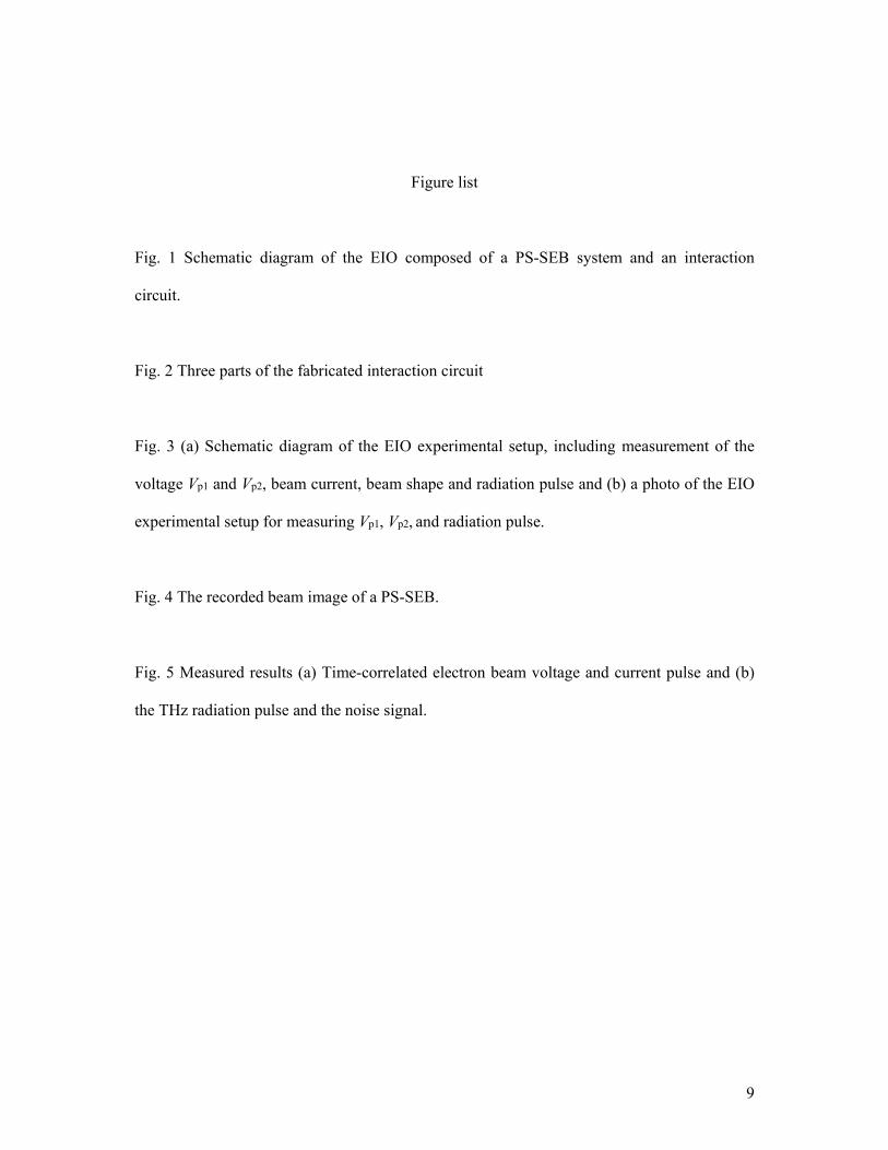
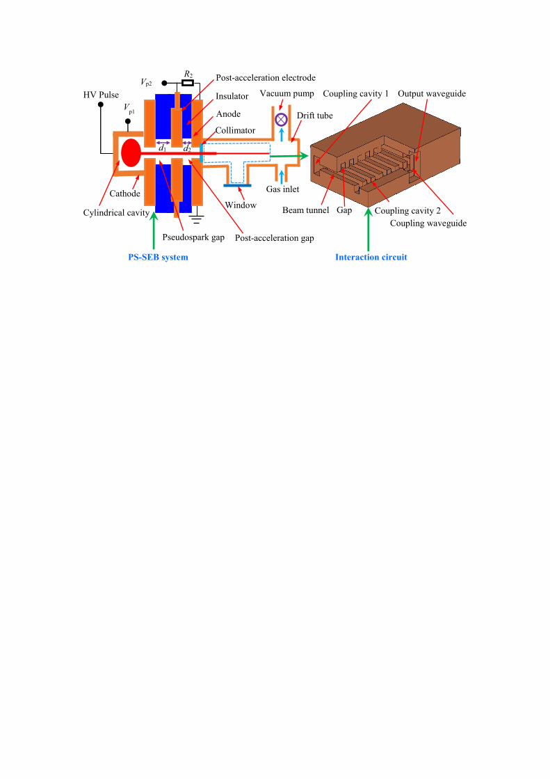
As shown in Fig. 1, the EIO was composed of a PS-SEB system and an interaction circuit.
The PS-SEB system consisted of a pseudospark discharge section and a post-acceleration
gap22. It was composed of a brass hollow cathode with a cylindrical cavity of 26 mm in
diameter and 12 mm in length, a perspex insulator of 16 mm thickness, a brass post-
acceleration electrode, a perspex insulator of 6 mm thickness and a brass planar anode,
resulting in the formation of a pseudospark discharge section and a post-acceleration gap. The
generated pencil PS-EB would propagate from the hollow cavity to the anode through an on-
axis aperture of 3 mm diameter. At the anode a rectangular collimator with the size of 2.0
mm×0.25 mm was used to form the PS-SEB. There are three main stages in a typical
pseudospark discharge, where a PS-EB with moderate beam current and high energy can be
obtained in the second hollow cathode stage (used for the beam-wave interaction in reference
5, 10-11). The beam current reaches its maximum in the third pseudospark discharge stage,
while the beam energy rapidly decreases due to the breakdown between the gaps. Post-
acceleration of the PS-EB generated in the third stage could result in combined high beam
current and energy (the most desirable electron beam for the beam-wave interaction), which
was implemented in this work by insertion of a post-acceleration electrode and a 200 Ω high
voltage resistor R2. The experiment of the post-acceleration related to this PS-SEB was
reported in reference 23.
To match and interact with the PS-SEB, a planar EIO circuit was used in our design. It had
the advantage that it could be machined by wire-cutting technology. The interaction circuit
was composed of a resonant SWS (including a rectangular beam tunnel, two coupling cavities
4
and eleven gaps) and an output coupling structure (consisting of a coupling waveguide and an
output waveguide).
To achieve a stable gas pressure, a rotary pump was used to evacuate the tube and the
operating gas (air in this case) entered the whole system through a fine adjustable needle
valve. The gas pressure was monitored by a vacuum gauge. A cylindrical aperture of 2 mm
diameter was drilled at the end of the interaction circuit to generate an exhaust path leading to
the drift tube. A standard rectangular waveguide WR-5 was connected to the interaction
circuit’s output waveguide, with the vacuum seal achieved by the use of a thin Mylar sheet
placed between them. A cylindrical tube filled with the interaction circuit was integrated with
the PS-SEB system using an “O” ring, thus achieving a complete EIO.
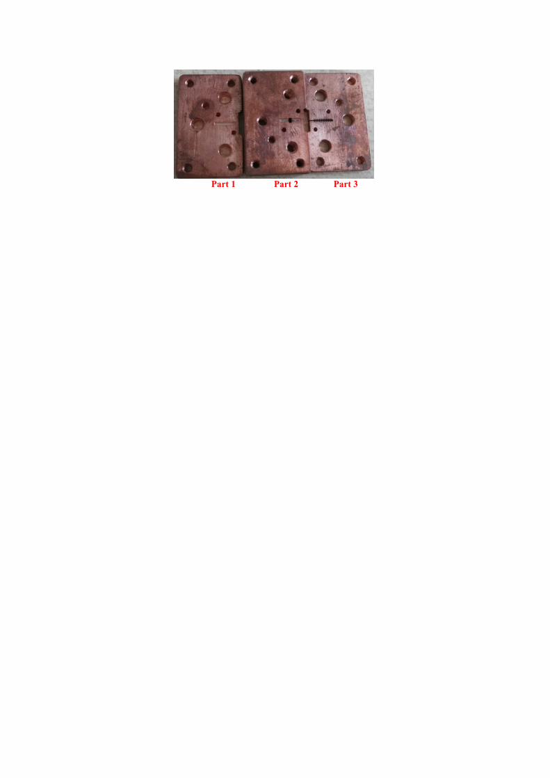
The expense for making a PS-SEB driven EIO was relatively low, due to some of its
advantages, such as the ease of fabrication of the device, low vacuum requirement and the fact
that an external focusing magnetic field would not be required. The PS-SEB system had
relatively large structural dimensions and its smallest part (the 3 mm cylindrical aperture) had
the property of axial symmetry enabling it to be manufactured easily by using a milling
machine. The fabrication challenge of the whole device was mainly due to the construction of
the interaction circuit. The optimized structural dimensions in reference 12 were used in our
experiment. It should be noted, to ease the fabrication using the electric discharge machining,
that the coupling waveguide in reference 12 was not used, instead the standard output
waveguide was directly connected to the resonant SWS, which would reduce the coupling
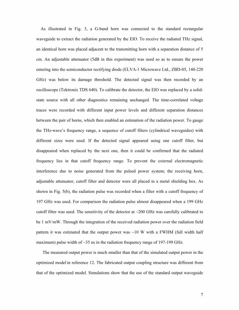
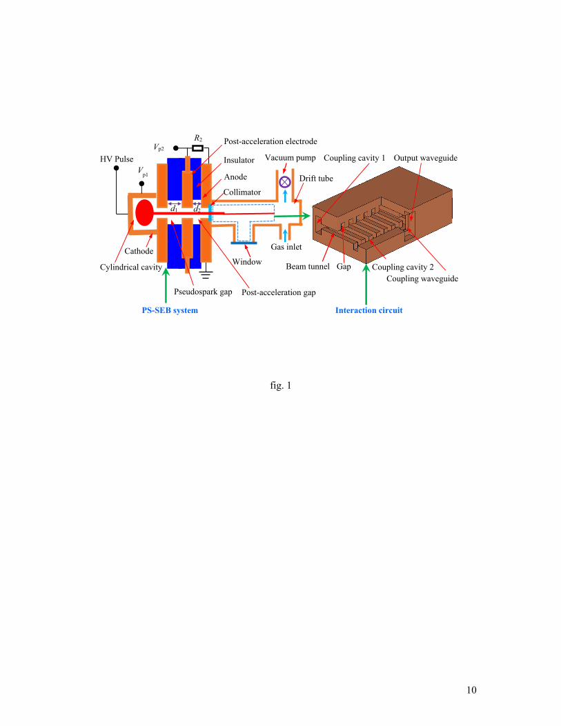
efficiency and thus result in a smaller measured radiation power. As shown in Fig. 2, the
interaction circuit has been divided into three parts. Part 1 and part 2 were fabricated by high
speed milling and the two rectangular waveguides in part 2 were first drilled with the final
geometry achieved by electrical discharge machining. The beam tunnel and eleven gaps in
part 3 were wire cut from a piece of copper block in one process (using tungsten wire of
5
diameter 30 µm). The assembled interaction circuit had a compact configuration with 3-D
dimensions of 28 mm×17 mm×5 mm. The reflection coefficient curve (S11) was measured
using a vector network analyzer (Anritsu 37397D) and a frequency extender (Anritsu
V05VNA2-T/R 140-220 GHz), and was in agreement with the simulation prediction12. The
operating mode (TM110-2π mode) had a resonant peak at ~197.8 GHz.
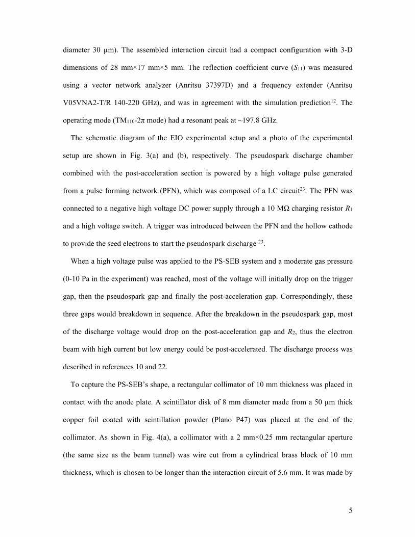
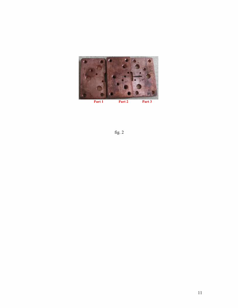
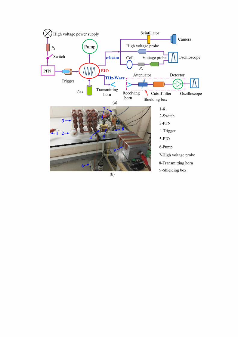
The schematic diagram of the EIO experimental setup and a photo of the experimental
setup are shown in Fig. 3(a) and (b), respectively. The pseudospark discharge chamber
combined with the post-acceleration section is powered by a high voltage pulse generated
from a pulse forming network (PFN), which was composed of a LC circuit23. The PFN was
connected to a negative high voltage DC power supply through a 10 MΩ charging resistor R1
and a high voltage switch. A trigger was introduced between the PFN and the hollow cathode
to provide the seed electrons to start the pseudospark discharge 23.
When a high voltage pulse was applied to the PS-SEB system and a moderate gas pressure
(0-10 Pa in the experiment) was reached, most of the voltage will initially drop on the trigger
gap, then the pseudospark gap and finally the post-acceleration gap. Correspondingly, these
three gaps would breakdown in sequence. After the breakdown in the pseudospark gap, most
of the discharge voltage would drop on the post-acceleration gap and R2, thus the electron
beam with high current but low energy could be post-accelerated. The discharge process was
described in references 10 and 22.
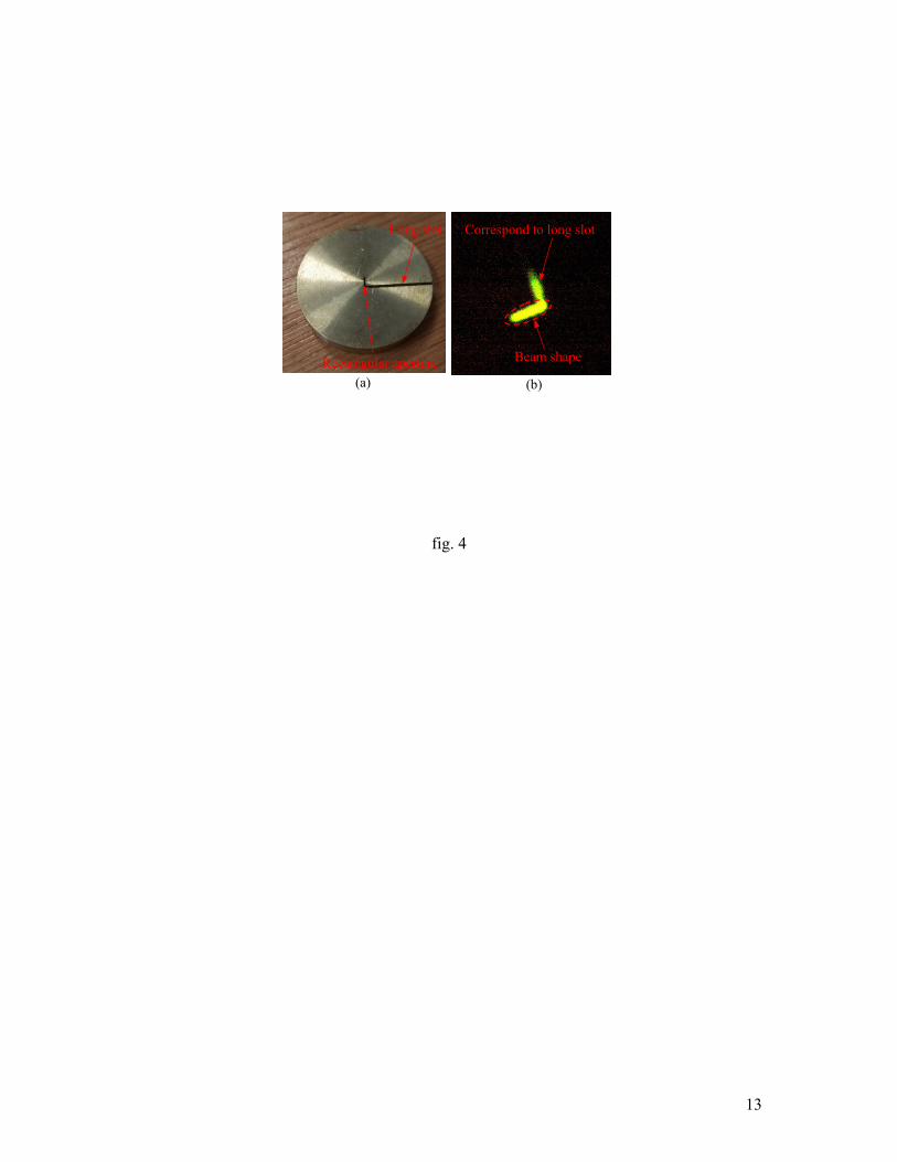
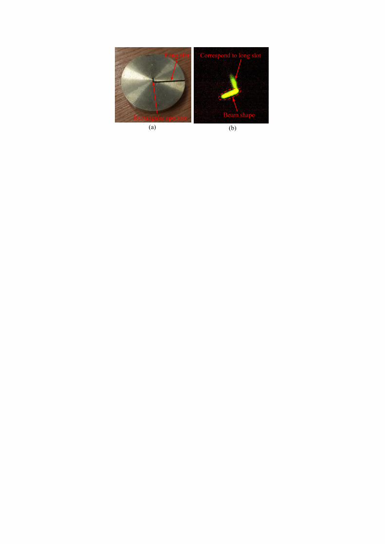
To capture the PS-SEB’s shape, a rectangular collimator of 10 mm thickness was placed in
contact with the anode plate. A scintillator disk of 8 mm diameter made from a 50 µm thick
copper foil coated with scintillation powder (Plano P47) was placed at the end of the
collimator. As shown in Fig. 4(a), a collimator with a 2 mm×0.25 mm rectangular aperture
(the same size as the beam tunnel) was wire cut from a cylindrical brass block of 10 mm
thickness, which is chosen to be longer than the interaction circuit of 5.6 mm. It was made by
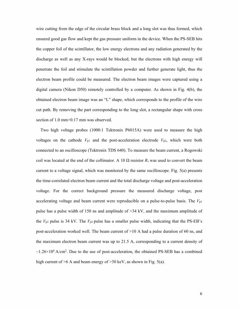
6
wire cutting from the edge of the circular brass block and a long slot was thus formed, which
ensured good gas flow and kept the gas pressure uniform in the device. When the PS-SEB hits
the copper foil of the scintillator, the low energy electrons and any radiation generated by the
discharge as well as any X-rays would be blocked, but the electrons with high energy will
penetrate the foil and stimulate the scintillation powder and further generate light, thus the
electron beam profile could be measured. The electron beam images were captured using a
digital camera (Nikon D50) remotely controlled by a computer. As shown in Fig. 4(b), the
obtained electron beam image was an “L” shape, which corresponds to the profile of the wire
cut path. By removing the part corresponding to the long slot, a rectangular shape with cross
section of 1.0 mm×0.17 mm was observed.
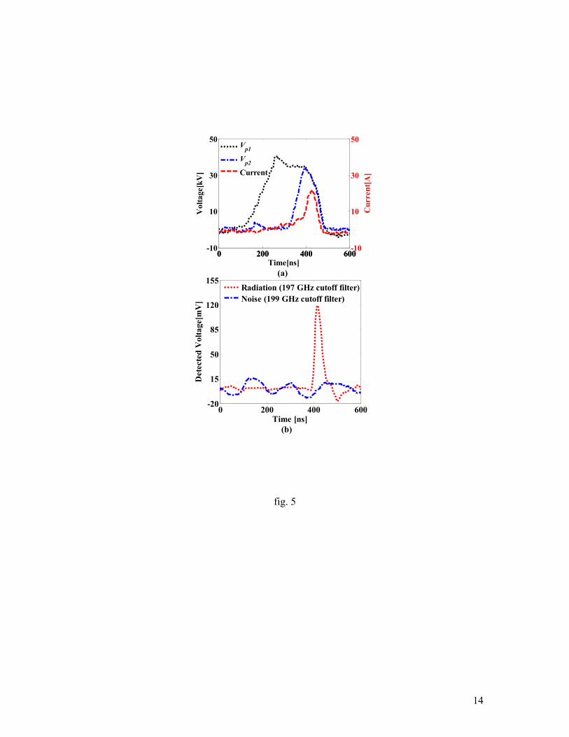
Two high voltage probes (1000:1 Tektronix P6015A) were used to measure the high
voltages on the cathode Vp1 and the post-acceleration electrode Vp2, which were both
connected to an oscilloscope (Tektronix TDS 640). To measure the beam current, a Rogowski
coil was located at the end of the collimator. A 10 Ω resistor Rs was used to convert the beam
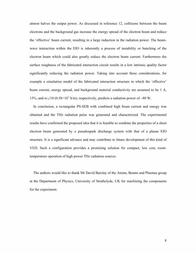
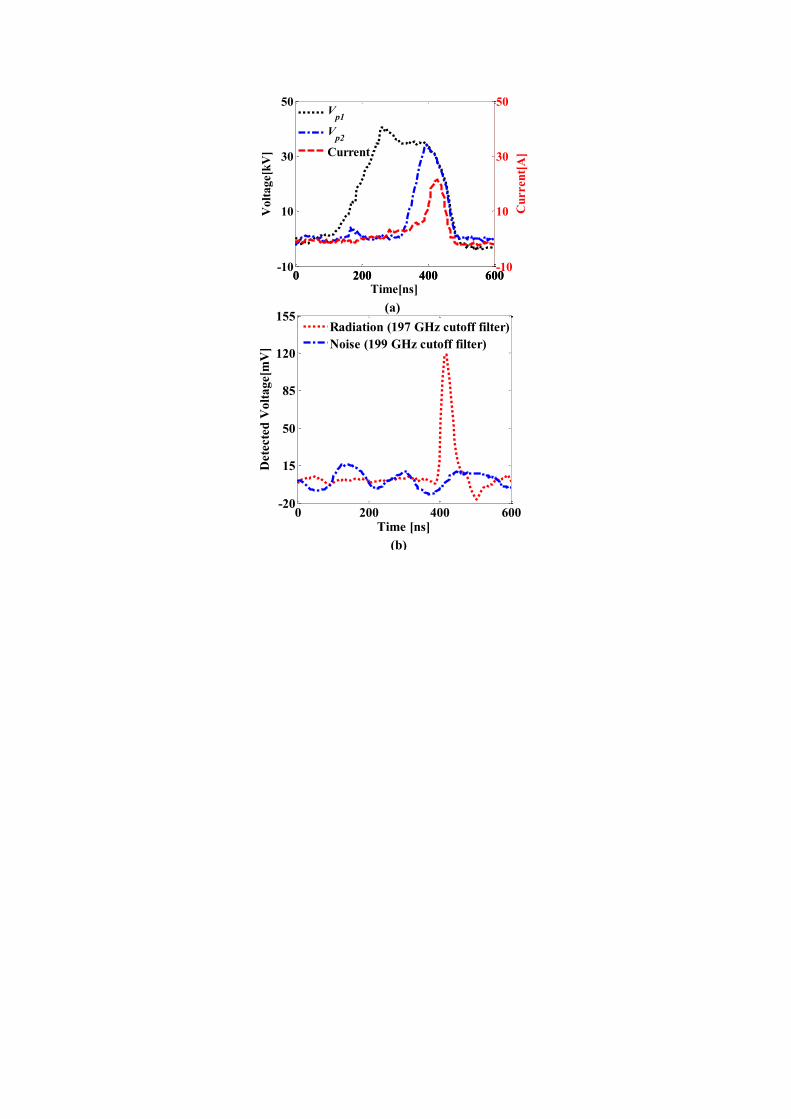
current to a voltage signal, which was monitored by the same oscilloscope. Fig. 5(a) presents
the time-correlated electron beam current and the total discharge voltage and post-acceleration
voltage. For the correct background pressure the measured discharge voltage, post
accelerating voltage and beam current were reproducible on a pulse-to-pulse basis. The Vp1
pulse has a pulse width of 150 ns and amplitude of >34 kV, and the maximum amplitude of
the Vp2 pulse is 34 kV. The Vp2 pulse has a smaller pulse width, indicating that the PS-EB’s
post-acceleration worked well. The beam current of >10 A had a pulse duration of 60 ns, and
the maximum electron beam current was up to 21.5 A, corresponding to a current density of
~1.26×10⁴ A/cm2. Due to the use of post-acceleration, the obtained PS-SEB has a combined
high current of >6 A and beam energy of >30 keV, as shown in Fig. 5(a).
7
As illustrated in Fig. 3, a G-band horn was connected to the standard rectangular
waveguide to extract the radiation generated by the EIO. To receive the radiated THz signal,
an identical horn was placed adjacent to the transmitting horn with a separation distance of 5
cm. An adjustable attenuator (5dB in this experiment) was used so as to ensure the power
entering into the semiconductor rectifying diode (ELVA-1 Microwave Ltd., ZBD-05, 140-220
GHz) was below its damage threshold. The detected signal was then recorded by an
oscilloscope (Tektronix TDS 640). To calibrate the detector, the EIO was replaced by a solid-
state source with all other diagnostics remaining unchanged. The time-correlated voltage
traces were recorded with different input power levels and different separation distances
between the pair of horns, which then enabled an estimation of the radiation power. To gauge
the THz-wave’s frequency range, a sequence of cutoff filters (cylindrical waveguides) with
different sizes were used. If the detected signal appeared using one cutoff filter, but
disappeared when replaced by the next one, then it could be confirmed that the radiated
frequency lies in that cutoff frequency range. To prevent the external electromagnetic
interference due to noise generated from the pulsed power system; the receiving horn,
adjustable attenuator, cutoff filter and detector were all placed in a metal shielding box. As
shown in Fig. 5(b), the radiation pulse was recorded when a filter with a cutoff frequency of
197 GHz was used. For comparison the radiation pulse almost disappeared when a 199 GHz
cutoff filter was used. The sensitivity of the detector at ~200 GHz was carefully calibrated to
be 1 mV/mW. Through the integration of the received radiation power over the radiation field
pattern it was estimated that the output power was ~10 W with a FWHM (full width half
maximum) pulse width of ~35 ns in the radiation frequency range of 197-199 GHz.
The measured output power is much smaller than that of the simulated output power in the
optimized model in reference 12. The fabricated output coupling structure was different from
that of the optimized model. Simulations show that the use of the standard output waveguide
8
almost halves the output power. As discussed in reference 12, collisions between the beam
electrons and the background gas increase the energy spread of the electron beam and reduce
the ‘effective’ beam current, resulting in a large reduction in the radiation power. The beam-
wave interaction within the EIO is inherently a process of instability or bunching of the
electron beam which could also greatly reduce the electron beam current. Furthermore the
surface roughness of the fabricated interaction circuit results in a low intrinsic quality factor
significantly reducing the radiation power. Taking into account these considerations, for
example a simulation model of the fabricated interaction structure in which the ‘effective’
beam current, energy spread, and background material conductivity are assumed to be 1 A,
15%, and σCu/10 (0.58×10⁷ S/m), respectively, predicts a radiation power of ~80 W.
In conclusion, a rectangular PS-SEB with combined high beam current and energy was
obtained and the THz radiation pulse was generated and characterized. The experimental
results have confirmed the proposed idea that it is feasible to combine the properties of a sheet
electron beam generated by a pseudospark discharge system with that of a planar EIO
structure. It is a significant advance and may contribute to future development of this kind of
VED. Such a configuration provides a promising solution for compact, low cost, room-
temperature operation of high power THz radiation sources.
The authors would like to thank Mr David Barclay of the Atoms, Beams and Plasmas group
at the Department of Physics, University of Strathclyde, UK for machining the components
for the experiment.
9
Figure list
Fig. 1 Schematic diagram of the EIO composed of a PS-SEB system and an interaction
circuit.
Fig. 2 Three parts of the fabricated interaction circuit
Fig. 3 (a) Schematic diagram of the EIO experimental setup, including measurement of the
voltage Vp1 and Vp2, beam current, beam shape and radiation pulse and (b) a photo of the EIO
experimental setup for measuring Vp1, Vp2, and radiation pulse.
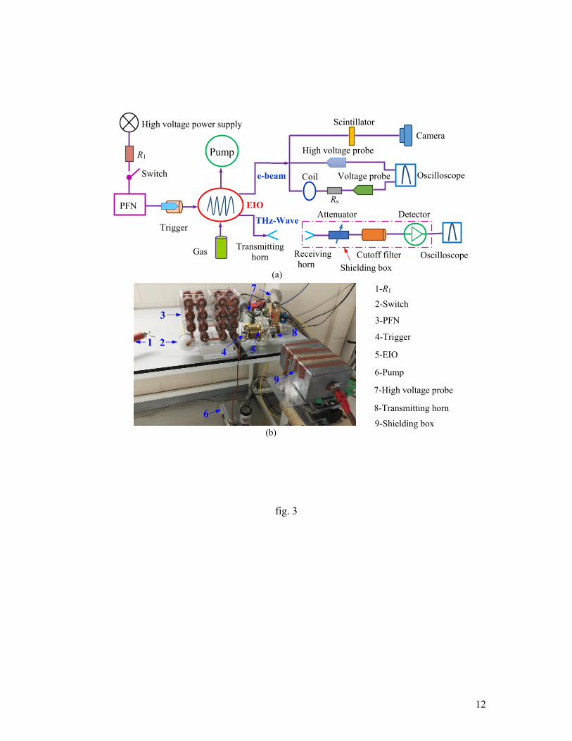
Fig. 4 The recorded beam image of a PS-SEB.
Fig. 5 Measured results (a) Time-correlated electron beam voltage and current pulse and (b)
the THz radiation pulse and the noise signal.
10
fig. 1
Gas inlet
HV Pulse
Cylindrical cavity
Collimator
Anode
Vacuum pump
Window
Output waveguide
Beam tunnel
Coupling cavity 1
Gap
Interaction circuit PS-SEB system
R2 Vp2
Vp1
Post-acceleration electrode
Insulator
Cathode
Pseudospark gap Post-acceleration gap
Coupling waveguideCoupling cavity 2
d1 d2
Drift tube
11
fig. 2
Part 2Part 1 Part 3
12
fig. 3
Attenuator
(b)
Shielding box
1-R1
Rs
High voltage probe
Scintillator
Coil Voltage probee-beam
Cutoff filter Oscilloscope
EIO
Pump
Transmitting
horn
Detector PFN
THz-Wave
Oscilloscope
Camera
Trigger
High voltage power supply
Switch
R1
Gas Receiving horn
1
2-Switch
3-PFN
(a)
2
3
5
6
7
8
9
4-Trigger
5-EIO
9-Shielding box
6-Pump
8-Transmitting horn
4
7-High voltage probe
13
fig. 4
(a) (b)
Rectangular aperture
Long slot Correspond to long slot
Beam shape
14
fig. 5
(a)
(b)
0 200 400 600-10
10
30
50
Time[ns]
Vol
tage
[kV
]
0 200 400 600-10
10
30
50
Cur
rent
[A]
Vp1
Vp2
Current
0 200 400 600-20
15
50
85
120
155
Time [ns]
Det
ecte
d V
olta
ge[m
V]
Radiation (197 GHz cutoff filter)Noise (199 GHz cutoff filter)
15
References
1E. Linfield, Nature Photon.1, 257 (2007). 2J. H. Booske, R. J. Dobbs, C. D. Joye, C. L. Kory, G. R. Neil, G. S. Park, J. Park, and R. J. Temkin, IEEE Trans. Terahertz Sci. Technol. 1, 54(2011).
3J. H. Booske, Phys. Plasmas 15, 055502 (2008). 4C. W. Baik, H. Y. Ahn, Y. Kim, J. Lee, S. Hong, S. H. Lee, J. H. Choi, S. Kim, S. Y. Jeon, S. Yu, G. Collins, M. E. Read, R. L. Ives, J. M. Kim, and S. Hwang, Appl. Phys. Lett. 107, 191109 (2015).
5Y. Yin, W. He, L. Zhang, H. Yin, C. W. Robertson, and A. W. Cross, IEEE Trans. Electron Devices 63, 512 (2016).
6P. Horoyski, A. Roitman, R. Dobbs, M. Hyttinen, H. Deng, 15th IEEE International Vacuum Electronics Conference (2014), pp. 221-222.
7W. X. Liu, C. Zhao, K. Li, Y. Wang, Z. Q. Yang, IEEE Trans. Electron Devices 61, 902 (2014).
8J. Christiansen and C. Schultheiss, Z. Phys. A 290, 35 (1979). 9W. W. Destler, Z. Segalov, J. Rodgers, K. Ramaswamy, and M. Reiser, Appl. Phys. Lett. 62, 1739 (1993).
10W. He, L. Zhang, D. Bowes, H. Yin, K. Ronald, A. D. R. Phelps, and A.W. Cross, Appl. Phys. Lett. 107, 133501 (2015).
11H. Yin, A. W. Cross, W. He, A. D. R. Phelps, K. Ronald, D. Bowes, and C. W. Robertson, Phys. Plasmas 16, 063105 (2009). 12G. Shu, W. He, L. Zhang, H. Yin, J. Zhao, A. W. Cross, and A. D. R. Phelps, IEEE Trans. Electron Devices 63, 4955 (2016).
13N. Kumar, D. K. Pal, R. P. Lamba, U.N. Pal and R. Prakash, IEEE Trans. Electron Devices 64, 2688 (2017). 14N. Kumar, D. K. Pal, A. S. Jadon, U. N. Pal, H. Rahaman and R. Prakash, Rev. Sci. Instr. 87, 033503 (2016). 15U. N. Pal, P. Shukla, A. S. Jadon, and N. Kumar, IEEE Trans. Plasma Sci., 99 (2017). 16C. Q. Jiang, A. Kuthi, M. A. Gundersen, and W. Hartmann, Appl. Phys. Lett. 87, 131501 (2005).
17A. Baig, D. Gamzina, T. Kimura, J. Atkinson, C. Domier, B. Popovic, L. Himes, R. Barchfeld, M. Field, N. C. Luhmann, Jr., IEEE Trans. Electron Devices 64, 2390 (2017).
16
18Y. M. Shin, A. Baig, R. Barchfeld, D. Gamzina, L. R. Barnett, and N. C. Luhmann, Jr., Appl. Phys. Lett. 100, 154103 (2012).
19J. Pasour, E. Wright, K. T. Nguyen, A. Balkcum, F. N. Wood, R. E. Myers, B. Levush, IEEE Trans. Electron Devices 61, 1630 (2014).
20Z. X. Zhang, W. W. Destler, V. L. Granatstein, T. M. Antonsen, Jr., B. Levush, J. Rodgers, and S. Cheng. Appl. Phys. Lett. 64, 1439 (2009).
21M. Mineo and C. Paoloni, IEEE Trans. Electron Devices 57, 1481 (2010). 22H. Yin, A. W. Cross, W. He, A. D. R. Phelps, and K. Ronald, IEEE Trans. Plasma Sci. 32, 233 (2004).
23J. Zhao, H. Yin, L. Zhang, G. Shu, W. He, Q. Zhang, A. D. R. Phelps, and A. W. Cross, Phys. Plasmas 24, 023105 (2017).
Gas inlet
HV Pulse
Cylindrical cavity
Collimator
Anode
Vacuum pump
Window
Output waveguide
Beam tunnel
Coupling cavity 1
Gap
Interaction circuit PS-SEB system
R2 Vp2
Vp1
Post-acceleration electrode
Insulator
Cathode
Pseudospark gap Post-acceleration gap
Coupling waveguide
Coupling cavity 2
d1
d2
Drift tube
Part 2 Part 1 Part 3
Attenuator
(b)
Shielding box
1-R1
Rs
High voltage probe
Scintillator
Coil Voltage probe e-beam
Cutoff filter Oscilloscope
EIO
Pump
f
adf
afa
Transmitting
horn
Detector PFN
THz-Wave
Oscilloscope
Camera
Trigger
High voltage power supply
Switch
R1
Gas Receiving
horn
P
FN
E
IO
(
b)
1
2-Switch
3-PFN
(a)
2
3
5
6
7
8
9
4-Trigger
5-EIO
9-Shielding box
6-Pump
8-Transmitting horn
4
7-High voltage probe
(a) (b)
Rectangular aperture
Long slot Correspond to long slot
Beam shape
0 200 400 600-10
10
30
50
Time[ns]
Vo
lta
ge[k
V]
0 200 400 600-10
10
30
50
Cu
rren
t[A
]
Vp1
Vp2
Current
0 200 400 600-20
15
50
85
120
155
Time [ns]
Dete
cte
d V
olt
age[m
V]
Radiation (197 GHz cutoff filter)
Noise (199 GHz cutoff filter)
(a)
(b)